EP3804028B1 - Stacked circuit boards within a lighting device - Google Patents
Stacked circuit boards within a lighting deviceDownload PDFInfo
- Publication number
- EP3804028B1 EP3804028B1EP19725168.9AEP19725168AEP3804028B1EP 3804028 B1EP3804028 B1EP 3804028B1EP 19725168 AEP19725168 AEP 19725168AEP 3804028 B1EP3804028 B1EP 3804028B1
- Authority
- EP
- European Patent Office
- Prior art keywords
- circuit board
- light emitting
- lighting device
- emitting element
- antenna
- Prior art date
- Legal status (The legal status is an assumption and is not a legal conclusion. Google has not performed a legal analysis and makes no representation as to the accuracy of the status listed.)
- Active
Links
Images


Classifications
- H—ELECTRICITY
- H01—ELECTRIC ELEMENTS
- H01Q—ANTENNAS, i.e. RADIO AERIALS
- H01Q1/00—Details of, or arrangements associated with, antennas
- H01Q1/12—Supports; Mounting means
- H01Q1/22—Supports; Mounting means by structural association with other equipment or articles
- F—MECHANICAL ENGINEERING; LIGHTING; HEATING; WEAPONS; BLASTING
- F21—LIGHTING
- F21V—FUNCTIONAL FEATURES OR DETAILS OF LIGHTING DEVICES OR SYSTEMS THEREOF; STRUCTURAL COMBINATIONS OF LIGHTING DEVICES WITH OTHER ARTICLES, NOT OTHERWISE PROVIDED FOR
- F21V23/00—Arrangement of electric circuit elements in or on lighting devices
- F21V23/04—Arrangement of electric circuit elements in or on lighting devices the elements being switches
- F21V23/0442—Arrangement of electric circuit elements in or on lighting devices the elements being switches activated by means of a sensor, e.g. motion or photodetectors
- F21V23/045—Arrangement of electric circuit elements in or on lighting devices the elements being switches activated by means of a sensor, e.g. motion or photodetectors the sensor receiving a signal from a remote controller
- F—MECHANICAL ENGINEERING; LIGHTING; HEATING; WEAPONS; BLASTING
- F21—LIGHTING
- F21V—FUNCTIONAL FEATURES OR DETAILS OF LIGHTING DEVICES OR SYSTEMS THEREOF; STRUCTURAL COMBINATIONS OF LIGHTING DEVICES WITH OTHER ARTICLES, NOT OTHERWISE PROVIDED FOR
- F21V23/00—Arrangement of electric circuit elements in or on lighting devices
- F21V23/003—Arrangement of electric circuit elements in or on lighting devices the elements being electronics drivers or controllers for operating the light source, e.g. for a LED array
- F21V23/004—Arrangement of electric circuit elements in or on lighting devices the elements being electronics drivers or controllers for operating the light source, e.g. for a LED array arranged on a substrate, e.g. a printed circuit board
- F—MECHANICAL ENGINEERING; LIGHTING; HEATING; WEAPONS; BLASTING
- F21—LIGHTING
- F21V—FUNCTIONAL FEATURES OR DETAILS OF LIGHTING DEVICES OR SYSTEMS THEREOF; STRUCTURAL COMBINATIONS OF LIGHTING DEVICES WITH OTHER ARTICLES, NOT OTHERWISE PROVIDED FOR
- F21V23/00—Arrangement of electric circuit elements in or on lighting devices
- F21V23/04—Arrangement of electric circuit elements in or on lighting devices the elements being switches
- F21V23/0442—Arrangement of electric circuit elements in or on lighting devices the elements being switches activated by means of a sensor, e.g. motion or photodetectors
- H—ELECTRICITY
- H01—ELECTRIC ELEMENTS
- H01Q—ANTENNAS, i.e. RADIO AERIALS
- H01Q1/00—Details of, or arrangements associated with, antennas
- H01Q1/12—Supports; Mounting means
- H01Q1/22—Supports; Mounting means by structural association with other equipment or articles
- H01Q1/2258—Supports; Mounting means by structural association with other equipment or articles used with computer equipment
- H01Q1/2275—Supports; Mounting means by structural association with other equipment or articles used with computer equipment associated to expansion card or bus, e.g. in PCMCIA, PC cards, Wireless USB
- H—ELECTRICITY
- H01—ELECTRIC ELEMENTS
- H01Q—ANTENNAS, i.e. RADIO AERIALS
- H01Q1/00—Details of, or arrangements associated with, antennas
- H01Q1/36—Structural form of radiating elements, e.g. cone, spiral, umbrella; Particular materials used therewith
- H01Q1/38—Structural form of radiating elements, e.g. cone, spiral, umbrella; Particular materials used therewith formed by a conductive layer on an insulating support
- H—ELECTRICITY
- H01—ELECTRIC ELEMENTS
- H01Q—ANTENNAS, i.e. RADIO AERIALS
- H01Q1/00—Details of, or arrangements associated with, antennas
- H01Q1/44—Details of, or arrangements associated with, antennas using equipment having another main function to serve additionally as an antenna, e.g. means for giving an antenna an aesthetic aspect
- H—ELECTRICITY
- H01—ELECTRIC ELEMENTS
- H01Q—ANTENNAS, i.e. RADIO AERIALS
- H01Q7/00—Loop antennas with a substantially uniform current distribution around the loop and having a directional radiation pattern in a plane perpendicular to the plane of the loop
- H—ELECTRICITY
- H01—ELECTRIC ELEMENTS
- H01Q—ANTENNAS, i.e. RADIO AERIALS
- H01Q9/00—Electrically-short antennas having dimensions not more than twice the operating wavelength and consisting of conductive active radiating elements
- H01Q9/04—Resonant antennas
- H—ELECTRICITY
- H01—ELECTRIC ELEMENTS
- H01Q—ANTENNAS, i.e. RADIO AERIALS
- H01Q9/00—Electrically-short antennas having dimensions not more than twice the operating wavelength and consisting of conductive active radiating elements
- H01Q9/04—Resonant antennas
- H01Q9/30—Resonant antennas with feed to end of elongated active element, e.g. unipole
- F—MECHANICAL ENGINEERING; LIGHTING; HEATING; WEAPONS; BLASTING
- F21—LIGHTING
- F21Y—INDEXING SCHEME ASSOCIATED WITH SUBCLASSES F21K, F21L, F21S and F21V, RELATING TO THE FORM OR THE KIND OF THE LIGHT SOURCES OR OF THE COLOUR OF THE LIGHT EMITTED
- F21Y2115/00—Light-generating elements of semiconductor light sources
- F21Y2115/10—Light-emitting diodes [LED]
Definitions
- the present disclosurerelates to the field of lighting devices.
- the present disclosurerelates to the field of lighting devices including one or more sensors and/or antennas.
- light emitting elementssuch as light bulbs or light emitting diodes, LEDs
- sensorsmay for example include presence detectors, which may be used to turn the light emitting elements on or off depending on whether a person is present in e.g. a particular room or area.
- presence detectorsmay for example use microwave radar technology, and require e.g. internal or external antennas several centimetres in size in order to match the wavelength of the transmitted (and received) radio waves.
- a lighting devicemay include several light emitting elements mounted on a circuit board.
- the circuit boardmay also include other components such as e.g. transformers, power regulators, and various passive components such as e.g. resistors, inductors and capacitors.
- the space remaining on the circuit boardmay therefore be limited, and the provision of the antenna for the presence detector may be impossible or difficult.
- the antennamay instead be positioned external to the lighting device, which for e.g. aesthetical reason may be less desirable. In some situations, the antenna may still be positioned within the lighting device, but at a suboptimal location in terms of technical function.
- US 2010/188301discloses a lamp apparatus including an optical unit and a patch antenna.
- the optical untincludes an LED and a substrate having the LED mounted at the front face, and a cover member having visible-light transmittance, spread over the LED at the front.
- the patch antennaincluding a patch element and a ground element located at the rear of the patch element.
- a communication interfaceincludes a communication board and a looped antenna.
- the communication boardis arranged to be covered by a housing and has an aperture portion.
- the looped antennais arranged on a circumferential edge of the aperture portion to be looped around the aperture portion.
- the light sourceincludes a light source board, arranged at a position opposite to the housing across the communication interface along a direction of thickness of the communication board, and a light source mounted on the light source board.
- the present disclosureprovides a lighting device as defined in the independent claim. Further embodiments of the lighting device are defined in the dependent claims.
- a lighting deviceincludes first circuit board.
- the first circuit boardincludes at least a first light emitting element and a second light emitting element mounted thereon (e.g. on a surface of the first circuit board).
- the lighting devicefurther includes a second circuit board.
- the second circuit boardincludes an aperture.
- the second circuit boardis arranged relative to the first circuit board such that the aperture is positioned to match a position of the first light emitting element but not a position of the second light emitting element.
- the lighting devicefurther includes a sensor and/or antenna.
- the sensor and/or antennamay e.g. form part of a control system for the lighting device. At least a part of the sensor and/or antenna is provided on a portion of the second circuit board which extends between the first light emitting element and the second light emitting element.
- the term "extending"may include also a partial extension, such as a portion of the second circuit board which may partially extend between the first light emitting element and the second light emitting element.
- the second circuit boardmay be shaped and arranged such that it, due to the aperture, does not block light emitted from the first light emitting element.
- the second circuit boardmay also be shaped and arranged such that it does not block light emitted from the second light emitting element.
- the senormay include the antenna. In some embodiments, only the antenna may be included. In some embodiments, both the antenna and the sensor may be included as separate components.
- the antennaif included, may for example be used for the sensor, or for other purposes such as e.g. radio frequency communication (e.g. for wireless communication between multiple lighting devices and/or between a lighting device and for example a master or modem/bridge module).
- the second circuit boardmay further include a second aperture.
- the second circuit boardmay be further arranged relative to the first circuit board such that the second aperture is positioned to match a position of the second light emitting element. Providing a second aperture may allow for the second circuit board to have an even larger area/space available for the sensor and/or antenna, without blocking light emitted by the light emitting elements.
- the second circuit boardmay be arranged in physical contact with the first circuit board (e.g. directly on top of the first circuit board). Arranging the second circuit board in (direct) physical contact with the first circuit board may for example allow to reduce the dimensions of the aperture (and the second aperture, if present) while still allowing light to pass through the aperture(s). This may result in an increased area/space available for the sensor and/or antenna.
- the second circuit boardmay be arranged at a distance from the first circuit board.
- the distancemay be such that light emitted by e.g. the first light emitting element may pass through the aperture (e.g. without being blocked).
- Arranging the second circuit board at a distance from the first circuit boardmay for example allow for an improved cooling of components on the first circuit board.
- a surface of the second circuit board facing away from the first circuit boardis flush with a surface of the first light emitting element facing away from the first circuit board. This may provide an increased transmission of light emitted by the first light emitting element through the aperture of the second circuit board.
- a surface of the second circuit board (or the first light emitting element)may be a surface which is opposite to a surface of the second circuit board (or the first light emitting element) which faces the first circuit board.
- the lighting devicemay include the antenna.
- the enlarged area/space, due to the positioning of the second circuit board on the first circuit board,may allow enough room for an antenna suitable for presence detectors operating at lower frequency (for example between 5 GHz and 15 GHz, or for example between 5 GHz and 10 GHz).
- Such (radar) presence detectorsmay be less complex and more cost efficient than detectors which may operate using smaller antennas but at increased frequencies (such as e.g. at 24 GHz or 77 GHz).
- the antennamay be a radar antenna and/or a radio frequency antenna.
- the antennamay for example be designed to operate at a frequency in the interval from 5 to 15 GHz.
- the antennamay for example be designed to operate in the 5 GHz and 10 GHz range.
- At least a part of the antennamay form at least one closed loop.
- the at least one closed loopmay surround the aperture of the second circuit board.
- the closed loopmay e.g. provide an improved functioning of the antenna, and the arrangement of the antenna (such that it surrounds the apertures) may allow for a further improved utilization of the available area/space on the second circuit board for the antenna.
- the at least one closed loopmay also surround more than one aperture, e.g. the second aperture (if present) of the second circuit board.
- the at least a part of the antennamay e.g. have a rectangular or circular shape.
- At least one of the first circuit board and the second circuit boardmay be a printed circuit board (PCB). It is envisaged also that, in some embodiments, circuit boards created using e.g. wire wrap and/or point-to-point construction may be used instead or in addition. In some embodiments, both of the first circuit board and the second circuit board may be PCBs.
- PCBprinted circuit board
- a material of the second circuit boardmay be different from a material of the first circuit board.
- the material of the second circuit boardmay for example be a material more suited for the sensor and/or antenna than the material of the first circuit board.
- the material of the second circuit boardmay for example be more expensive than the material of the first circuit board, and only using this more expensive material in the second circuit board may provide an improved cost efficiency.
- At least one of the first light emitting element and the second light emitting elementmay be a light emitting diode (LED). It is envisaged also that, in some embodiments, other light emitting elements may be used. In some embodiments, both of the first light emitting element and the second light emitting element may be LEDs. Using LEDs to produce light may be beneficial e.g. in terms of energy efficiency.
- the lighting devicemay include a tube.
- the tubemay be transparent or translucent to light emitted by the first lighting emitting element and/or the second light emitting element.
- the tubemay be transparent or translucent to light emitted by both the first lighting element and the second light emitting element.
- the first circuit board and the second circuit boardmay be arranged within the tube.
- the lighting device including the tubemay for example be a tubular LED (TLED), wherein LEDs are used as light emitting elements and the tube is shaped like that of a tube of a fluorescent lamp.
- TLEDtubular LED
- the sensor and/or antennamay be integrated into the TLED at a more optimal location (such as in the middle of the tube, instead of at e.g. an endcap of the tube or similar) while still providing transmission (i.e. non-blocking) of light emitted by the light emitting elements. This may for example also improve the functionality of the presence detector also when the TLED is mounted in a luminaire.
- the first light emitting element and the second light emitting elementmay form part of a plurality of LEDs mounted in a linear pattern on the first circuit board.
- a distance between neighbouring LEDsmay for example be between 1 to 2 centimetres.
- the present disclosureprovides arranging the second circuit board such that the space/area between two light emitting elements may be utilized for the antenna (of e.g. a presence detector), while still (due to one or more apertures of the second circuit board) allowing light emitted from light emitting elements to be transmitted without being blocked by the second circuit board.
- the antennaof e.g. a presence detector
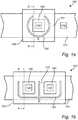
- FIG. 1aschematically illustrates a lighting device 100 as seen from above.
- the lighting device 100includes a first circuit board 110 and a second circuit board 120. At least a first light emitting element 130 and a second light emitting element 132 are mounted on the first circuit board 110.
- the first and second light emitting elements 130 and 132are LEDs.
- the first circuit board 110may also include other components (not shown) such as e.g. wiring to transport electrical current to/from the first and second LEDs 130 and 132.
- the second circuit board 120is arranged above the first circuit board 110 and has an aperture 140, and is arranged relative to the first circuit board 110 such that a position of the aperture 140 matches a position of the first light emitting element (or LED) 130 but not of the second light emitting element (or LED) 132.
- the lighting device 100includes an antenna 150. At least a part of the antenna 150 is provided on a portion 121 of the second circuit board 120. The portion 121 of the second circuit board 120 extends between the first lighting element 130 and the second lighting element 132.
- the first circuit board 110may for example be a printed circuit board (PCB).
- the second circuit board 120may for example also be a PCB. It is envisaged also that, in some embodiments, a material of the second circuit board 120 may for example be different from a material of the first circuit board 110, and adapted to the type of sensor (such as the antenna 150) provided on the second circuit board 120. It is envisaged also that, in some embodiments, the material of the first circuit board 110 may be the same or similar to the material of the second circuit board 120.
- FIG 1bschematically illustrates a lighting device 101 as seen from above.
- the lighting device 101is similar to the lighting device 100 described with reference to Figure 1a , except that the second circuit board 122 of the lighting device 101 (compared to the second circuit board 120 of the lighting device 100) also includes a second aperture 142.
- the second circuit board 122is further arranged relative to the first circuit board 110 such that a position of the second aperture 142 matches a position of the second light emitting element 132.
- the sensor(in form of the antenna 151) is E-shaped and arranged such that at least a part of the antenna 151 is provided on a portion 123 of the second circuit board 122.
- the portion 123 of the second circuit board 122extends between the first light emitting element 130 and the second light emitting element 132.
- an antennasuch as the antenna 150 or 151
- an antennamay have other forms, but that at least one or more parts of the sensor/antenna are provided on a portion of the second circuit board which extends between at least two light emitting elements.
- integration of sensors/antennas several centimetres in sizemay be provided.
- the antenna 150may for example be a radar antenna or an antenna for radio frequency (RF) communication.
- RFradio frequency
- the antennamay be replaced, or complemented with, e.g. one or more sensors, which may also benefit from the increased available space/surface for their installation due to the arrangement of a second circuit board on a first circuit board.
- Figures 1c and 1dillustrate schematically the lighting devices 100 and 101 as seen from the side, towards the cutting plane A-A (as indicated in the respective Figures 1a and 1b ).
- the second circuit board 120 or 122is arranged in physical contact with (i.e. directly above, or on top of) the first circuit board 110. This may provide e.g. an optimal transmission (i.e. minimal blocking) of light emitted by e.g. the first light emitting element 130 through the aperture 140.
- the surfaces of the second circuit board 120 or 122 and the light emitting element 130 which face away from the surface of the first circuit board 110i.e. the surfaces opposite to the surfaces of the second circuit board 120 or 122 and the light emitting element 130 which face towards the first circuit board 110) are flush. Phrased differently, the light emitting element 130 is not below the top surface of the second circuit board 120 or 122.
- the top surface of the second circuit board 120 or 122is slightly above the top surface of the light emitting element 130, but not enough to affect the transmission of light through the aperture 140 of the second circuit board 120 or 122.
- the second circuit board 120 or 122is arranged at a distance from the first circuit board 110, using e.g. on or more spacer elements 112. Although the top surface of the second circuit board 120 or 122 is no longer flush with the top surface of the light emitting element 130, the distance is still small enough not to block the light emitted from the light emitting element 130. In the embodiment of the lighting device 100 or 101 illustrated in Figure 1d , it may also be envisaged that the second circuit board 120 or 122 is still arranged at a distance from the first circuit board 110, but that the thickness of the second circuit board 120 or 122 is such that the top surfaces are still flush.
- Figures 2a and 2billustrate schematically embodiments of respective lighting devices 200 and 201, wherein the respective antennas 250 and 251 have different shapes.
- the antenna 250includes a closed loop and is arranged on the second circuit board 220 such that it surrounds the aperture 240.
- the antenna 250has a circular shape.
- the antenna 251also includes a closed loop, and the antenna 251 is also arranged on the second circuit board 220 such that it surrounds the aperture 240.
- the antenna 251has a rectangular shape.
- At least parts of the antennas 250 and 251are provided on portions 221 of the second circuit boards 220 which extend between the first light emitting element 230 and the second light emitting element 232.
- TLEDtubular LED
- FIG 3aillustrates schematically a lighting device 300 as seen from above.
- the lighting device 300includes a tube 360 which is transparent or translucent to light emitted from a plurality of light emitting elements of the lighting device 300.
- five such light emitting elementsare illustrated as LEDs 330, 332, 334, 336 and 338.
- the LEDs 330-338are arranged/mounted in a linear pattern on a first circuit board (PCB) 310 of the lighting device 300.
- the lighting device 300may for example be a TLED.
- the lighting device 300also includes a second circuit board 320 which is arranged above the first circuit board 310.
- the second circuit board 320includes an aperture 340 which is positioned to match a position of a first light emitting element (LED) 330.
- the size and shape of the aperture 340is such that light emitted by the first light emitting element 330 may escape through the aperture 340 without being blocked. It is envisaged that the second circuit board 320 may, for this reason, for example be arranged directly on top of (e.g. in physical contact with) the first circuit board 310.
- the second circuit board 320extends between the first light emitting element 330 and a second light emitting element 332.
- the aperture 340is positioned such that its position does not match the position of the second light emitting element 332, i.e. such that a portion 321 of the second circuit board 320 between the first and second light emitting elements 330 and 332 may be utilized as a space/area in which a sensor and/or antenna may be installed/provided.
- the lighting device 300includes an antenna 350.
- the antenna 350has a circular shape and includes a loop which surrounds the aperture 340.
- the antenna 350has other shapes which may also fit due to utilization of the additional space/area provided by the portion 321 of the second circuit board 320 extending between light emitting elements.
- the second circuit board 320may, in some embodiments, include more than one aperture, and that the positions of these additional apertures may match those of other light emitting elements than the LED 330.
- the second circuit board 320may include a second aperture, and the second circuit board 320 may be arranged such that the position of the second aperture (not shown) matches that of the second light emitting element (LED) 332.
- Figure 3billustrates schematically a view of the lighting device 300 as seen from the side, towards the cutting plane B-B indicated in Figure 3a .
- the first circuit board 310 and the second circuit board 320are arranged within the tube 360.
- the second circuit board 320is arranged on top of the first circuit board 310, and the arrangement of the first and second circuit boards 310 and 320 within the tube 360 allows, as described earlier herein, to position e.g. the sensor (antenna 350) at a more optimal location within the tube 360.
- the antenna 350may be replaced by, or complemented with, e.g. one or more sensors which may benefit from the additional area/space made available by the arrangement of the second circuit board 320 on the first circuit board 310.
- the present disclosureallows to utilize the space/area available between the light emitting elements more efficiently. This may allow for sensors/antennas which would normally not fit on the first circuit board to be used and included within the lighting device. As an example, as provided herein, this may allow to provide a tubular LED (TLED) having an antenna which is located more optimally (e.g. towards the middle of the tube), instead of placing the antenna towards (or in) an endcap of the tube, or as an external antenna. In addition to technical and/or aesthetical reasons, this may also allow to use antennas suitable for presence detectors operating at lower frequencies, thereby reducing the cost of such detectors and the cost and/or complexity of the lighting device itself.
- TLEDtubular LED
Landscapes
- Engineering & Computer Science (AREA)
- General Engineering & Computer Science (AREA)
- Computer Networks & Wireless Communication (AREA)
- Computer Hardware Design (AREA)
- Microelectronics & Electronic Packaging (AREA)
- Arrangement Of Elements, Cooling, Sealing, Or The Like Of Lighting Devices (AREA)
- Circuit Arrangement For Electric Light Sources In General (AREA)
- Non-Portable Lighting Devices Or Systems Thereof (AREA)
- Fastening Of Light Sources Or Lamp Holders (AREA)
- Combinations Of Printed Boards (AREA)
- Support Of Aerials (AREA)
Description
- The present disclosure relates to the field of lighting devices. In particular, the present disclosure relates to the field of lighting devices including one or more sensors and/or antennas.
- To dynamically control lighting systems, light emitting elements (such as light bulbs or light emitting diodes, LEDs) may be combined with one or more sensors. Such sensors may for example include presence detectors, which may be used to turn the light emitting elements on or off depending on whether a person is present in e.g. a particular room or area. To detect the presence of the person, presence detectors may for example use microwave radar technology, and require e.g. internal or external antennas several centimetres in size in order to match the wavelength of the transmitted (and received) radio waves.
- A lighting device may include several light emitting elements mounted on a circuit board. In addition to the light emitting elements themselves, the circuit board may also include other components such as e.g. transformers, power regulators, and various passive components such as e.g. resistors, inductors and capacitors. The space remaining on the circuit board may therefore be limited, and the provision of the antenna for the presence detector may be impossible or difficult. The antenna may instead be positioned external to the lighting device, which for e.g. aesthetical reason may be less desirable. In some situations, the antenna may still be positioned within the lighting device, but at a suboptimal location in terms of technical function.
- In light of the above, there is therefore a need for an improved way of providing a sensor and/or antenna in combination with a lighting device.
US 2010/188301 discloses a lamp apparatus including an optical unit and a patch antenna. The optical unt includes an LED and a substrate having the LED mounted at the front face, and a cover member having visible-light transmittance, spread over the LED at the front. In this optical unit are stored the patch antenna including a patch element and a ground element located at the rear of the patch element.US2018/101110 discloses an image forming apparatus. A communication interface includes a communication board and a looped antenna. The communication board is arranged to be covered by a housing and has an aperture portion. The looped antenna is arranged on a circumferential edge of the aperture portion to be looped around the aperture portion. The light source includes a light source board, arranged at a position opposite to the housing across the communication interface along a direction of thickness of the communication board, and a light source mounted on the light source board.- To at least partly satisfy the above needs, the present disclosure provides a lighting device as defined in the independent claim. Further embodiments of the lighting device are defined in the dependent claims.
- According to an aspect of the present disclosure, a lighting device is provided. The lighting device includes first circuit board. The first circuit board includes at least a first light emitting element and a second light emitting element mounted thereon (e.g. on a surface of the first circuit board).
- The lighting device further includes a second circuit board. The second circuit board includes an aperture. The second circuit board is arranged relative to the first circuit board such that the aperture is positioned to match a position of the first light emitting element but not a position of the second light emitting element.
- The lighting device further includes a sensor and/or antenna. The sensor and/or antenna may e.g. form part of a control system for the lighting device. At least a part of the sensor and/or antenna is provided on a portion of the second circuit board which extends between the first light emitting element and the second light emitting element. Here, the term "extending" may include also a partial extension, such as a portion of the second circuit board which may partially extend between the first light emitting element and the second light emitting element. The second circuit board may be shaped and arranged such that it, due to the aperture, does not block light emitted from the first light emitting element. The second circuit board may also be shaped and arranged such that it does not block light emitted from the second light emitting element.
- Providing a second circuit board may allow for an enlarged area/space available for the sensor and/or antenna, without (due to the aperture in the second circuit board) blocking or limiting light emitted from the first light emitting element. Phrased differently, the provision of the second circuit board may allow to better utilize the area/space between the light emitting elements for positioning of the sensor and/or antenna. In some embodiments, the sensor may include the antenna. In some embodiments, only the antenna may be included. In some embodiments, both the antenna and the sensor may be included as separate components. The antenna, if included, may for example be used for the sensor, or for other purposes such as e.g. radio frequency communication (e.g. for wireless communication between multiple lighting devices and/or between a lighting device and for example a master or modem/bridge module).
- In some embodiments, the second circuit board may further include a second aperture. The second circuit board may be further arranged relative to the first circuit board such that the second aperture is positioned to match a position of the second light emitting element. Providing a second aperture may allow for the second circuit board to have an even larger area/space available for the sensor and/or antenna, without blocking light emitted by the light emitting elements.
- In some embodiments, the second circuit board may be arranged in physical contact with the first circuit board (e.g. directly on top of the first circuit board). Arranging the second circuit board in (direct) physical contact with the first circuit board may for example allow to reduce the dimensions of the aperture (and the second aperture, if present) while still allowing light to pass through the aperture(s). This may result in an increased area/space available for the sensor and/or antenna.
- In some embodiments, the second circuit board may be arranged at a distance from the first circuit board. Depending on for example the size of the aperture, the distance may be such that light emitted by e.g. the first light emitting element may pass through the aperture (e.g. without being blocked). Arranging the second circuit board at a distance from the first circuit board may for example allow for an improved cooling of components on the first circuit board.
- A surface of the second circuit board facing away from the first circuit board is flush with a surface of the first light emitting element facing away from the first circuit board. This may provide an increased transmission of light emitted by the first light emitting element through the aperture of the second circuit board. Herein, a surface of the second circuit board (or the first light emitting element) may be a surface which is opposite to a surface of the second circuit board (or the first light emitting element) which faces the first circuit board.
- In some embodiments, the lighting device may include the antenna. The enlarged area/space, due to the positioning of the second circuit board on the first circuit board, may allow enough room for an antenna suitable for presence detectors operating at lower frequency (for example between 5 GHz and 15 GHz, or for example between 5 GHz and 10 GHz). Such (radar) presence detectors may be less complex and more cost efficient than detectors which may operate using smaller antennas but at increased frequencies (such as e.g. at 24 GHz or 77 GHz).
- In some embodiments, the antenna may be a radar antenna and/or a radio frequency antenna. The antenna may for example be designed to operate at a frequency in the interval from 5 to 15 GHz. The antenna may for example be designed to operate in the 5 GHz and 10 GHz range.
- In some embodiments, at least a part of the antenna may form at least one closed loop. The at least one closed loop may surround the aperture of the second circuit board. The closed loop may e.g. provide an improved functioning of the antenna, and the arrangement of the antenna (such that it surrounds the apertures) may allow for a further improved utilization of the available area/space on the second circuit board for the antenna. In some embodiments, the at least one closed loop may also surround more than one aperture, e.g. the second aperture (if present) of the second circuit board.
- In some embodiments, the at least a part of the antenna may e.g. have a rectangular or circular shape.
- In some embodiments, at least one of the first circuit board and the second circuit board may be a printed circuit board (PCB). It is envisaged also that, in some embodiments, circuit boards created using e.g. wire wrap and/or point-to-point construction may be used instead or in addition. In some embodiments, both of the first circuit board and the second circuit board may be PCBs.
- In some embodiments, a material of the second circuit board may be different from a material of the first circuit board. The material of the second circuit board may for example be a material more suited for the sensor and/or antenna than the material of the first circuit board. The material of the second circuit board may for example be more expensive than the material of the first circuit board, and only using this more expensive material in the second circuit board may provide an improved cost efficiency.
- In some embodiments, at least one of the first light emitting element and the second light emitting element may be a light emitting diode (LED). It is envisaged also that, in some embodiments, other light emitting elements may be used. In some embodiments, both of the first light emitting element and the second light emitting element may be LEDs. Using LEDs to produce light may be beneficial e.g. in terms of energy efficiency.
- In some embodiments, the lighting device may include a tube. The tube may be transparent or translucent to light emitted by the first lighting emitting element and/or the second light emitting element. For example, the tube may be transparent or translucent to light emitted by both the first lighting element and the second light emitting element. The first circuit board and the second circuit board may be arranged within the tube. In some embodiments, the lighting device including the tube may for example be a tubular LED (TLED), wherein LEDs are used as light emitting elements and the tube is shaped like that of a tube of a fluorescent lamp. By providing the sensor and/or antenna not on the first circuit board but at the second circuit board containing the aperture, the sensor and/or antenna may be integrated into the TLED at a more optimal location (such as in the middle of the tube, instead of at e.g. an endcap of the tube or similar) while still providing transmission (i.e. non-blocking) of light emitted by the light emitting elements. This may for example also improve the functionality of the presence detector also when the TLED is mounted in a luminaire.
- In some embodiments, the first light emitting element and the second light emitting element may form part of a plurality of LEDs mounted in a linear pattern on the first circuit board. A distance between neighbouring LEDs may for example be between 1 to 2 centimetres. By providing the sensor and/or antenna on the second circuit board, and by arranging the second circuit board such that the one or more apertures allow light emitted by the LEDs to pass therethrough without being blocked, the sensor and/or antenna may be provided inside (i.e. as an integrated part) of the TLED.
- As described herein, the present disclosure provides arranging the second circuit board such that the space/area between two light emitting elements may be utilized for the antenna (of e.g. a presence detector), while still (due to one or more apertures of the second circuit board) allowing light emitted from light emitting elements to be transmitted without being blocked by the second circuit board.
- Exemplifying embodiments will be described below with reference to the accompanying drawings, in which:
Fig. 1a schematically illustrates a lighting device according to embodiments of the present disclosure;Fig. 1b schematically illustrates a lighting device according to embodiments of the present disclosure;Fig. 1c schematically illustrates a cross-section of the lighting device inFigure 1a or 1b ;Fig. 1d schematically illustrates a cross-section of the lighting device inFigure 1a or 1b ;Fig. 2a schematically illustrates a lighting device according to embodiments of the present disclosure;Fig. 2b schematically illustrates a lighting device according to embodiments of the present disclosure;Fig. 3a schematically illustrates a lighting device according to embodiments of the present disclosure, andFig. 3b schematically illustrates a cross-section of the lighting device inFigure 3a .- In the drawings, like reference numerals will be used for like elements unless stated otherwise. Unless explicitly stated to the contrary, the drawings show only such elements that are necessary to illustrate the example embodiments, while other elements, in the interest of clarity, may be omitted or merely suggested. As illustrated in the figures, the sizes of elements and regions may be exaggerated for illustrative purposes and, thus, are provided to illustrate the general structures of the embodiments.
- Exemplifying embodiments will now be described more fully hereinafter with reference to the accompanying drawings.
- With reference to
Figure 1a , a lighting device according to an embodiment of the present disclosure is described in the following. Figure 1a schematically illustrates alighting device 100 as seen from above. Thelighting device 100 includes afirst circuit board 110 and asecond circuit board 120. At least a firstlight emitting element 130 and a secondlight emitting element 132 are mounted on thefirst circuit board 110. In the illustrated embodiment, the first and secondlight emitting elements first circuit board 110 may also include other components (not shown) such as e.g. wiring to transport electrical current to/from the first andsecond LEDs - The
second circuit board 120 is arranged above thefirst circuit board 110 and has anaperture 140, and is arranged relative to thefirst circuit board 110 such that a position of theaperture 140 matches a position of the first light emitting element (or LED) 130 but not of the second light emitting element (or LED) 132. - The
lighting device 100 includes anantenna 150. At least a part of theantenna 150 is provided on aportion 121 of thesecond circuit board 120. Theportion 121 of thesecond circuit board 120 extends between thefirst lighting element 130 and thesecond lighting element 132. - The
first circuit board 110 may for example be a printed circuit board (PCB). Thesecond circuit board 120 may for example also be a PCB. It is envisaged also that, in some embodiments, a material of thesecond circuit board 120 may for example be different from a material of thefirst circuit board 110, and adapted to the type of sensor (such as the antenna 150) provided on thesecond circuit board 120. It is envisaged also that, in some embodiments, the material of thefirst circuit board 110 may be the same or similar to the material of thesecond circuit board 120. - With reference to
Figure 1b , a lighting device according to another embodiment of the present disclosure is described in the following. Figure 1b schematically illustrates alighting device 101 as seen from above. Thelighting device 101 is similar to thelighting device 100 described with reference toFigure 1a , except that thesecond circuit board 122 of the lighting device 101 (compared to thesecond circuit board 120 of the lighting device 100) also includes asecond aperture 142. Thesecond circuit board 122 is further arranged relative to thefirst circuit board 110 such that a position of thesecond aperture 142 matches a position of the secondlight emitting element 132. The sensor (in form of the antenna 151) is E-shaped and arranged such that at least a part of theantenna 151 is provided on aportion 123 of thesecond circuit board 122. Theportion 123 of thesecond circuit board 122 extends between the firstlight emitting element 130 and the secondlight emitting element 132.- As will be described later herein, it is envisaged also that, in some embodiments, an antenna (such as the
antenna 150 or 151) may have other forms, but that at least one or more parts of the sensor/antenna are provided on a portion of the second circuit board which extends between at least two light emitting elements. By utilizing the space between light emitting elements, integration of sensors/antennas several centimetres in size may be provided. - The
antenna 150 may for example be a radar antenna or an antenna for radio frequency (RF) communication. - It is envisaged also that, in some embodiments, the antenna may be replaced, or complemented with, e.g. one or more sensors, which may also benefit from the increased available space/surface for their installation due to the arrangement of a second circuit board on a first circuit board.
Figures 1c and 1d illustrate schematically thelighting devices Figures 1a and 1b ).- In
Figure 1c , thesecond circuit board first circuit board 110. This may provide e.g. an optimal transmission (i.e. minimal blocking) of light emitted by e.g. the firstlight emitting element 130 through theaperture 140. The surfaces of thesecond circuit board light emitting element 130 which face away from the surface of the first circuit board 110 (i.e. the surfaces opposite to the surfaces of thesecond circuit board light emitting element 130 which face towards the first circuit board 110) are flush. Phrased differently, thelight emitting element 130 is not below the top surface of thesecond circuit board aperture 140. It may be envisaged also, in some embodiments, that the top surface of thesecond circuit board light emitting element 130, but not enough to affect the transmission of light through theaperture 140 of thesecond circuit board - In
Figure 1d , thesecond circuit board first circuit board 110, using e.g. on or morespacer elements 112. Although the top surface of thesecond circuit board light emitting element 130, the distance is still small enough not to block the light emitted from thelight emitting element 130. In the embodiment of thelighting device Figure 1d , it may also be envisaged that thesecond circuit board first circuit board 110, but that the thickness of thesecond circuit board - With reference to
Figures 2a ,2b and 2c, further embodiments of lighting devices according to the present disclosure will be described below. Figures 2a and2b illustrate schematically embodiments ofrespective lighting devices respective antennas - In
Figure 2a , theantenna 250 includes a closed loop and is arranged on thesecond circuit board 220 such that it surrounds theaperture 240. Theantenna 250 has a circular shape. - In
Figure 2b , theantenna 251 also includes a closed loop, and theantenna 251 is also arranged on thesecond circuit board 220 such that it surrounds theaperture 240. Theantenna 251 has a rectangular shape. - In both of the embodiments of the
lighting devices antennas portions 221 of thesecond circuit boards 220 which extend between the firstlight emitting element 230 and the secondlight emitting element 232. - With reference to
Figures 3a and3b , an embodiment of a lighting device in the form of a tubular LED (TLED) will be described in the following. Figure 3a illustrates schematically alighting device 300 as seen from above. Thelighting device 300 includes atube 360 which is transparent or translucent to light emitted from a plurality of light emitting elements of thelighting device 300. InFigure 3a , five such light emitting elements are illustrated asLEDs lighting device 300. Thelighting device 300 may for example be a TLED.- The
lighting device 300 also includes asecond circuit board 320 which is arranged above thefirst circuit board 310. Thesecond circuit board 320 includes anaperture 340 which is positioned to match a position of a first light emitting element (LED) 330. The size and shape of theaperture 340 is such that light emitted by the firstlight emitting element 330 may escape through theaperture 340 without being blocked. It is envisaged that thesecond circuit board 320 may, for this reason, for example be arranged directly on top of (e.g. in physical contact with) thefirst circuit board 310. - The
second circuit board 320 extends between the firstlight emitting element 330 and a secondlight emitting element 332. Theaperture 340 is positioned such that its position does not match the position of the secondlight emitting element 332, i.e. such that aportion 321 of thesecond circuit board 320 between the first and secondlight emitting elements - Provided on the
portion 321, thelighting device 300 includes anantenna 350. In the embodiment of thelighting device 300 as illustrated inFigure 3a , theantenna 350 has a circular shape and includes a loop which surrounds theaperture 340. As described herein, it may be envisaged also that, in some embodiments, theantenna 350 has other shapes which may also fit due to utilization of the additional space/area provided by theportion 321 of thesecond circuit board 320 extending between light emitting elements. It is, in addition, envisaged also that thesecond circuit board 320 may, in some embodiments, include more than one aperture, and that the positions of these additional apertures may match those of other light emitting elements than theLED 330. For example, thesecond circuit board 320 may include a second aperture, and thesecond circuit board 320 may be arranged such that the position of the second aperture (not shown) matches that of the second light emitting element (LED) 332. Figure 3b illustrates schematically a view of thelighting device 300 as seen from the side, towards the cutting plane B-B indicated inFigure 3a .- The
first circuit board 310 and thesecond circuit board 320 are arranged within thetube 360. Thesecond circuit board 320 is arranged on top of thefirst circuit board 310, and the arrangement of the first andsecond circuit boards tube 360 allows, as described earlier herein, to position e.g. the sensor (antenna 350) at a more optimal location within thetube 360. - As described earlier herein, in some embodiments, the
antenna 350 may be replaced by, or complemented with, e.g. one or more sensors which may benefit from the additional area/space made available by the arrangement of thesecond circuit board 320 on thefirst circuit board 310. - By providing a sensor and/or antenna on a second circuit board which may be arranged on top of a first circuit board and provided with one or more apertures through which light emitted by light emitting elements (e.g. LEDs) mounted on the first circuit board may pass without being blocked, the present disclosure allows to utilize the space/area available between the light emitting elements more efficiently. This may allow for sensors/antennas which would normally not fit on the first circuit board to be used and included within the lighting device. As an example, as provided herein, this may allow to provide a tubular LED (TLED) having an antenna which is located more optimally (e.g. towards the middle of the tube), instead of placing the antenna towards (or in) an endcap of the tube, or as an external antenna. In addition to technical and/or aesthetical reasons, this may also allow to use antennas suitable for presence detectors operating at lower frequencies, thereby reducing the cost of such detectors and the cost and/or complexity of the lighting device itself.
Claims (13)
- A lighting device (100), comprising:a first circuit board (110), comprising at least a first light emitting element (130) and a second light emitting element (132) mounted thereon;a second circuit board (120) comprising an aperture (140), and being arranged relative to the first circuit board such that the aperture is positioned to match a position of the first light emitting element but not a position of the second light emitting element; anda sensor and/or antenna (150), wherein at least a part of said sensor and/or antenna is provided on a portion (121) of the second circuit board extending between the first light emitting element and the second light emitting element,characterised in thata surface of the second circuit board facing away from the first circuit board is flush with a surface of the first light emitting element facing away from the first circuit board.
- The lighting device of claim 1, wherein the second circuit board further comprises a second aperture (142),
wherein the second circuit board is further arranged relative to the first circuit board such that the second aperture is positioned to match a position of the second light emitting element. - The lighting device of claim 1 or 2, wherein the second circuit board is arranged in physical contact with the first circuit board.
- The lighting device of claim 1 or 2, wherein the second circuit board is arranged at a distance from the first circuit board.
- The lighting device of any one of the preceding claims, wherein the lighting device includes the antenna.
- The lighting device of claim 5, wherein the antenna is a radar antenna and/or a radio frequency antenna.
- The lighting device of claim 5 or 6, wherein at least a part of the antenna forms at least one closed loop surrounding the aperture of the second circuit board.
- The lighting device of claim 7, wherein said at least a part of the antenna has a rectangular or circular shape.
- The lighting device of any one of the preceding claims, wherein at least one of the first circuit board and the second circuit board is a printed circuit board, PCB.
- The lighting device of any one of the preceding claims, wherein a material of the second circuit board is different from a material of the first circuit board.
- The lighting device of any one of the preceding claims, wherein at least one of the first light emitting element and the second light emitting element is a light emitting diode, LED.
- The lighting device of any one of the preceding claims, wherein said lighting device comprises a tube (360) which is transparent or translucent to light emitted by the first light emitting element and the second light emitting element, and wherein the first circuit board and the second circuit board are arranged within said tube.
- The lighting device of claim 12, wherein the first light emitting element and the second light emitting element form part of a plurality of light emitting diodes, LEDs, mounted in a linear pattern on the first circuit board.
Applications Claiming Priority (2)
| Application Number | Priority Date | Filing Date | Title |
|---|---|---|---|
| EP18175334 | 2018-05-31 | ||
| PCT/EP2019/063087WO2019228859A1 (en) | 2018-05-31 | 2019-05-21 | Stacked circuit boards within a lighting device |
Publications (2)
| Publication Number | Publication Date |
|---|---|
| EP3804028A1 EP3804028A1 (en) | 2021-04-14 |
| EP3804028B1true EP3804028B1 (en) | 2021-12-29 |
Family
ID=62495615
Family Applications (1)
| Application Number | Title | Priority Date | Filing Date |
|---|---|---|---|
| EP19725168.9AActiveEP3804028B1 (en) | 2018-05-31 | 2019-05-21 | Stacked circuit boards within a lighting device |
Country Status (5)
| Country | Link |
|---|---|
| US (1) | US11143393B2 (en) |
| EP (1) | EP3804028B1 (en) |
| JP (1) | JP6922107B2 (en) |
| CN (1) | CN112204813B (en) |
| WO (1) | WO2019228859A1 (en) |
Families Citing this family (3)
| Publication number | Priority date | Publication date | Assignee | Title |
|---|---|---|---|---|
| JP7617546B2 (en)* | 2020-04-20 | 2025-01-20 | パナソニックIpマネジメント株式会社 | Lighting fixtures |
| CN114651372A (en)* | 2020-11-13 | 2022-06-21 | 深圳市大疆创新科技有限公司 | Antenna module and unmanned aerial vehicle |
| US20240006739A1 (en)* | 2020-12-04 | 2024-01-04 | Sensormatic Electronics, LLC | Antennas with light source |
Family Cites Families (19)
| Publication number | Priority date | Publication date | Assignee | Title |
|---|---|---|---|---|
| CN101743573B (en)* | 2007-07-17 | 2014-05-14 | 住友电气工业株式会社 | Lamp device, antenna unit for a lamp device, communication system, and traffic signal controller |
| JP2012529143A (en)* | 2009-06-05 | 2012-11-15 | コーニンクレッカ フィリップス エレクトロニクス エヌ ヴィ | Lighting device with built-in RF antenna |
| KR101126211B1 (en) | 2010-07-15 | 2012-03-22 | (주)지티씨 | LED Microwave Sensor Lighting |
| CN103189684B (en)* | 2010-10-29 | 2016-08-17 | 欧司朗股份有限公司 | Light fixture |
| EP2837057B1 (en)* | 2012-04-12 | 2016-06-08 | Koninklijke Philips N.V. | Controllable lighting assembly |
| KR101360678B1 (en)* | 2012-07-23 | 2014-02-10 | 엘지이노텍 주식회사 | Lighting device |
| EP2768074A1 (en)* | 2013-02-18 | 2014-08-20 | BAE Systems PLC | Integrated lighting and network interface device |
| CN105122544B (en)* | 2013-04-23 | 2017-04-12 | 飞利浦照明控股有限公司 | Lighting installations including antennas and lamps |
| RU2631338C2 (en)* | 2014-03-21 | 2017-09-21 | Филипс Лайтинг Холдинг Б.В. | Optical structure, lighting unit and manufacture method |
| CN103912810A (en) | 2014-04-03 | 2014-07-09 | 生迪光电科技股份有限公司 | LED (light emitting diode) illuminating device, LED illuminating system and method for arranging antenna in LED illuminating device |
| US9356185B2 (en)* | 2014-06-20 | 2016-05-31 | Heptagon Micro Optics Pte. Ltd. | Compact light sensing modules including reflective surfaces to enhance light collection and/or emission, and methods of fabricating such modules |
| US10352541B2 (en)* | 2015-01-30 | 2019-07-16 | Signify Holding B.V. | Integrated smart module architecture |
| CN104633505A (en)* | 2015-03-06 | 2015-05-20 | 北京幻腾科技有限公司 | LED lighting equipment supporting wireless transmission |
| RU2653572C1 (en)* | 2015-03-17 | 2018-05-15 | Филипс Лайтинг Холдинг Б.В. | Lighting device with the first and second related and mutually movable antennas |
| WO2017005435A1 (en)* | 2015-07-06 | 2017-01-12 | Philips Lighting Holding B.V. | Lighting device with wireless control element |
| JP6575228B2 (en)* | 2015-08-24 | 2019-09-18 | 株式会社村田製作所 | Antenna module and wireless communication device |
| US10355340B2 (en)* | 2016-06-07 | 2019-07-16 | Signify Holding B.V. | Solid-state lighting device having a wireless communication antenna |
| JP2018060090A (en) | 2016-10-06 | 2018-04-12 | ブラザー工業株式会社 | Image forming apparatus |
| US10422860B2 (en)* | 2017-11-20 | 2019-09-24 | Stmicroelectronics Pte Ltd | Proximity sensor with integrated ALS |
- 2019
- 2019-05-21EPEP19725168.9Apatent/EP3804028B1/enactiveActive
- 2019-05-21CNCN201980036066.7Apatent/CN112204813B/enactiveActive
- 2019-05-21WOPCT/EP2019/063087patent/WO2019228859A1/ennot_activeCeased
- 2019-05-21USUS17/057,679patent/US11143393B2/enactiveActive
- 2019-05-21JPJP2020565818Apatent/JP6922107B2/enactiveActive
Also Published As
| Publication number | Publication date |
|---|---|
| US11143393B2 (en) | 2021-10-12 |
| US20210199274A1 (en) | 2021-07-01 |
| JP2021519504A (en) | 2021-08-10 |
| CN112204813A (en) | 2021-01-08 |
| WO2019228859A1 (en) | 2019-12-05 |
| CN112204813B (en) | 2024-05-17 |
| JP6922107B2 (en) | 2021-08-18 |
| EP3804028A1 (en) | 2021-04-14 |
Similar Documents
| Publication | Publication Date | Title |
|---|---|---|
| EP3804028B1 (en) | Stacked circuit boards within a lighting device | |
| US8013347B2 (en) | Remote control lighting assembly and use thereof | |
| US10794586B2 (en) | Communication cables with illumination | |
| RU2653572C1 (en) | Lighting device with the first and second related and mutually movable antennas | |
| CN105122544B (en) | Lighting installations including antennas and lamps | |
| KR101999660B1 (en) | The lighting apparatus having the communication module | |
| RU2672052C2 (en) | Lighting device and lamps containing integrated antenna | |
| US9635742B2 (en) | LED lighting device and system containing antenna, and related configuring method | |
| WO2015183591A1 (en) | Radio frequency (rf) signal pathway for a lamp antenna | |
| US20190312346A1 (en) | Antenna, Lighting System, And Communications System | |
| EP3036474B1 (en) | A luminary with a wireless transmitter | |
| JP6731501B2 (en) | Solid-state lighting device with wireless communication antenna | |
| JP6526264B2 (en) | lighting equipment | |
| JP6278004B2 (en) | lighting equipment | |
| JP6899546B2 (en) | lighting equipment | |
| EP2925091B1 (en) | Spotlight LED module and light module | |
| CN106151888A (en) | Light source cell and the ligthing paraphernalia including this light source cell | |
| JP7489050B2 (en) | Light | |
| US20240006739A1 (en) | Antennas with light source | |
| EP4269871A1 (en) | Led module and luminaire | |
| JP2018133315A (en) | Lighting drive device and light fitting | |
| JP2022181686A (en) | Luminaires and lighting systems | |
| JP2024070146A (en) | lighting equipment |
Legal Events
| Date | Code | Title | Description |
|---|---|---|---|
| STAA | Information on the status of an ep patent application or granted ep patent | Free format text:STATUS: UNKNOWN | |
| STAA | Information on the status of an ep patent application or granted ep patent | Free format text:STATUS: THE INTERNATIONAL PUBLICATION HAS BEEN MADE | |
| PUAI | Public reference made under article 153(3) epc to a published international application that has entered the european phase | Free format text:ORIGINAL CODE: 0009012 | |
| STAA | Information on the status of an ep patent application or granted ep patent | Free format text:STATUS: REQUEST FOR EXAMINATION WAS MADE | |
| 17P | Request for examination filed | Effective date:20210111 | |
| AK | Designated contracting states | Kind code of ref document:A1 Designated state(s):AL AT BE BG CH CY CZ DE DK EE ES FI FR GB GR HR HU IE IS IT LI LT LU LV MC MK MT NL NO PL PT RO RS SE SI SK SM TR | |
| AX | Request for extension of the european patent | Extension state:BA ME | |
| GRAP | Despatch of communication of intention to grant a patent | Free format text:ORIGINAL CODE: EPIDOSNIGR1 | |
| STAA | Information on the status of an ep patent application or granted ep patent | Free format text:STATUS: GRANT OF PATENT IS INTENDED | |
| RIC1 | Information provided on ipc code assigned before grant | Ipc:H01Q 1/22 20060101AFI20210707BHEP Ipc:H01Q 9/04 20060101ALI20210707BHEP Ipc:H01Q 1/38 20060101ALI20210707BHEP Ipc:H01Q 1/44 20060101ALI20210707BHEP Ipc:H01Q 7/00 20060101ALI20210707BHEP Ipc:H01Q 9/30 20060101ALI20210707BHEP Ipc:F21V 23/04 20060101ALI20210707BHEP Ipc:F21Y 115/10 20160101ALN20210707BHEP | |
| DAV | Request for validation of the european patent (deleted) | ||
| DAX | Request for extension of the european patent (deleted) | ||
| INTG | Intention to grant announced | Effective date:20210723 | |
| RIC1 | Information provided on ipc code assigned before grant | Ipc:H01Q 1/22 20060101AFI20210712BHEP Ipc:H01Q 9/04 20060101ALI20210712BHEP Ipc:H01Q 1/38 20060101ALI20210712BHEP Ipc:H01Q 1/44 20060101ALI20210712BHEP Ipc:H01Q 7/00 20060101ALI20210712BHEP Ipc:H01Q 9/30 20060101ALI20210712BHEP Ipc:F21V 23/04 20060101ALI20210712BHEP Ipc:F21Y 115/10 20160101ALN20210712BHEP | |
| GRAS | Grant fee paid | Free format text:ORIGINAL CODE: EPIDOSNIGR3 | |
| GRAA | (expected) grant | Free format text:ORIGINAL CODE: 0009210 | |
| STAA | Information on the status of an ep patent application or granted ep patent | Free format text:STATUS: THE PATENT HAS BEEN GRANTED | |
| AK | Designated contracting states | Kind code of ref document:B1 Designated state(s):AL AT BE BG CH CY CZ DE DK EE ES FI FR GB GR HR HU IE IS IT LI LT LU LV MC MK MT NL NO PL PT RO RS SE SI SK SM TR | |
| REG | Reference to a national code | Ref country code:GB Ref legal event code:FG4D | |
| REG | Reference to a national code | Ref country code:CH Ref legal event code:EP | |
| REG | Reference to a national code | Ref country code:AT Ref legal event code:REF Ref document number:1459365 Country of ref document:AT Kind code of ref document:T Effective date:20220115 | |
| REG | Reference to a national code | Ref country code:IE Ref legal event code:FG4D | |
| REG | Reference to a national code | Ref country code:DE Ref legal event code:R096 Ref document number:602019010511 Country of ref document:DE | |
| REG | Reference to a national code | Ref country code:LT Ref legal event code:MG9D | |
| PG25 | Lapsed in a contracting state [announced via postgrant information from national office to epo] | Ref country code:RS Free format text:LAPSE BECAUSE OF FAILURE TO SUBMIT A TRANSLATION OF THE DESCRIPTION OR TO PAY THE FEE WITHIN THE PRESCRIBED TIME-LIMIT Effective date:20211229 Ref country code:LT Free format text:LAPSE BECAUSE OF FAILURE TO SUBMIT A TRANSLATION OF THE DESCRIPTION OR TO PAY THE FEE WITHIN THE PRESCRIBED TIME-LIMIT Effective date:20211229 Ref country code:FI Free format text:LAPSE BECAUSE OF FAILURE TO SUBMIT A TRANSLATION OF THE DESCRIPTION OR TO PAY THE FEE WITHIN THE PRESCRIBED TIME-LIMIT Effective date:20211229 Ref country code:BG Free format text:LAPSE BECAUSE OF FAILURE TO SUBMIT A TRANSLATION OF THE DESCRIPTION OR TO PAY THE FEE WITHIN THE PRESCRIBED TIME-LIMIT Effective date:20220329 | |
| REG | Reference to a national code | Ref country code:AT Ref legal event code:MK05 Ref document number:1459365 Country of ref document:AT Kind code of ref document:T Effective date:20211229 | |
| PG25 | Lapsed in a contracting state [announced via postgrant information from national office to epo] | Ref country code:SE Free format text:LAPSE BECAUSE OF FAILURE TO SUBMIT A TRANSLATION OF THE DESCRIPTION OR TO PAY THE FEE WITHIN THE PRESCRIBED TIME-LIMIT Effective date:20211229 Ref country code:NO Free format text:LAPSE BECAUSE OF FAILURE TO SUBMIT A TRANSLATION OF THE DESCRIPTION OR TO PAY THE FEE WITHIN THE PRESCRIBED TIME-LIMIT Effective date:20220329 Ref country code:LV Free format text:LAPSE BECAUSE OF FAILURE TO SUBMIT A TRANSLATION OF THE DESCRIPTION OR TO PAY THE FEE WITHIN THE PRESCRIBED TIME-LIMIT Effective date:20211229 Ref country code:HR Free format text:LAPSE BECAUSE OF FAILURE TO SUBMIT A TRANSLATION OF THE DESCRIPTION OR TO PAY THE FEE WITHIN THE PRESCRIBED TIME-LIMIT Effective date:20211229 Ref country code:GR Free format text:LAPSE BECAUSE OF FAILURE TO SUBMIT A TRANSLATION OF THE DESCRIPTION OR TO PAY THE FEE WITHIN THE PRESCRIBED TIME-LIMIT Effective date:20220330 | |
| PG25 | Lapsed in a contracting state [announced via postgrant information from national office to epo] | Ref country code:NL Free format text:LAPSE BECAUSE OF FAILURE TO SUBMIT A TRANSLATION OF THE DESCRIPTION OR TO PAY THE FEE WITHIN THE PRESCRIBED TIME-LIMIT Effective date:20211229 | |
| PG25 | Lapsed in a contracting state [announced via postgrant information from national office to epo] | Ref country code:SM Free format text:LAPSE BECAUSE OF FAILURE TO SUBMIT A TRANSLATION OF THE DESCRIPTION OR TO PAY THE FEE WITHIN THE PRESCRIBED TIME-LIMIT Effective date:20211229 Ref country code:SK Free format text:LAPSE BECAUSE OF FAILURE TO SUBMIT A TRANSLATION OF THE DESCRIPTION OR TO PAY THE FEE WITHIN THE PRESCRIBED TIME-LIMIT Effective date:20211229 Ref country code:RO Free format text:LAPSE BECAUSE OF FAILURE TO SUBMIT A TRANSLATION OF THE DESCRIPTION OR TO PAY THE FEE WITHIN THE PRESCRIBED TIME-LIMIT Effective date:20211229 Ref country code:PT Free format text:LAPSE BECAUSE OF FAILURE TO SUBMIT A TRANSLATION OF THE DESCRIPTION OR TO PAY THE FEE WITHIN THE PRESCRIBED TIME-LIMIT Effective date:20220429 Ref country code:ES Free format text:LAPSE BECAUSE OF FAILURE TO SUBMIT A TRANSLATION OF THE DESCRIPTION OR TO PAY THE FEE WITHIN THE PRESCRIBED TIME-LIMIT Effective date:20211229 Ref country code:EE Free format text:LAPSE BECAUSE OF FAILURE TO SUBMIT A TRANSLATION OF THE DESCRIPTION OR TO PAY THE FEE WITHIN THE PRESCRIBED TIME-LIMIT Effective date:20211229 Ref country code:CZ Free format text:LAPSE BECAUSE OF FAILURE TO SUBMIT A TRANSLATION OF THE DESCRIPTION OR TO PAY THE FEE WITHIN THE PRESCRIBED TIME-LIMIT Effective date:20211229 | |
| PG25 | Lapsed in a contracting state [announced via postgrant information from national office to epo] | Ref country code:PL Free format text:LAPSE BECAUSE OF FAILURE TO SUBMIT A TRANSLATION OF THE DESCRIPTION OR TO PAY THE FEE WITHIN THE PRESCRIBED TIME-LIMIT Effective date:20211229 Ref country code:AT Free format text:LAPSE BECAUSE OF FAILURE TO SUBMIT A TRANSLATION OF THE DESCRIPTION OR TO PAY THE FEE WITHIN THE PRESCRIBED TIME-LIMIT Effective date:20211229 | |
| PG25 | Lapsed in a contracting state [announced via postgrant information from national office to epo] | Ref country code:IS Free format text:LAPSE BECAUSE OF FAILURE TO SUBMIT A TRANSLATION OF THE DESCRIPTION OR TO PAY THE FEE WITHIN THE PRESCRIBED TIME-LIMIT Effective date:20220429 | |
| REG | Reference to a national code | Ref country code:DE Ref legal event code:R097 Ref document number:602019010511 Country of ref document:DE | |
| PG25 | Lapsed in a contracting state [announced via postgrant information from national office to epo] | Ref country code:DK Free format text:LAPSE BECAUSE OF FAILURE TO SUBMIT A TRANSLATION OF THE DESCRIPTION OR TO PAY THE FEE WITHIN THE PRESCRIBED TIME-LIMIT Effective date:20211229 Ref country code:AL Free format text:LAPSE BECAUSE OF FAILURE TO SUBMIT A TRANSLATION OF THE DESCRIPTION OR TO PAY THE FEE WITHIN THE PRESCRIBED TIME-LIMIT Effective date:20211229 | |
| PLBE | No opposition filed within time limit | Free format text:ORIGINAL CODE: 0009261 | |
| STAA | Information on the status of an ep patent application or granted ep patent | Free format text:STATUS: NO OPPOSITION FILED WITHIN TIME LIMIT | |
| 26N | No opposition filed | Effective date:20220930 | |
| REG | Reference to a national code | Ref country code:CH Ref legal event code:PL | |
| REG | Reference to a national code | Ref country code:BE Ref legal event code:MM Effective date:20220531 | |
| PG25 | Lapsed in a contracting state [announced via postgrant information from national office to epo] | Ref country code:MC Free format text:LAPSE BECAUSE OF FAILURE TO SUBMIT A TRANSLATION OF THE DESCRIPTION OR TO PAY THE FEE WITHIN THE PRESCRIBED TIME-LIMIT Effective date:20211229 Ref country code:LU Free format text:LAPSE BECAUSE OF NON-PAYMENT OF DUE FEES Effective date:20220521 Ref country code:LI Free format text:LAPSE BECAUSE OF NON-PAYMENT OF DUE FEES Effective date:20220531 Ref country code:CH Free format text:LAPSE BECAUSE OF NON-PAYMENT OF DUE FEES Effective date:20220531 | |
| PG25 | Lapsed in a contracting state [announced via postgrant information from national office to epo] | Ref country code:SI Free format text:LAPSE BECAUSE OF FAILURE TO SUBMIT A TRANSLATION OF THE DESCRIPTION OR TO PAY THE FEE WITHIN THE PRESCRIBED TIME-LIMIT Effective date:20211229 | |
| PG25 | Lapsed in a contracting state [announced via postgrant information from national office to epo] | Ref country code:IE Free format text:LAPSE BECAUSE OF NON-PAYMENT OF DUE FEES Effective date:20220521 | |
| PG25 | Lapsed in a contracting state [announced via postgrant information from national office to epo] | Ref country code:IT Free format text:LAPSE BECAUSE OF FAILURE TO SUBMIT A TRANSLATION OF THE DESCRIPTION OR TO PAY THE FEE WITHIN THE PRESCRIBED TIME-LIMIT Effective date:20211229 Ref country code:BE Free format text:LAPSE BECAUSE OF NON-PAYMENT OF DUE FEES Effective date:20220531 | |
| P01 | Opt-out of the competence of the unified patent court (upc) registered | Effective date:20230425 | |
| PG25 | Lapsed in a contracting state [announced via postgrant information from national office to epo] | Ref country code:MK Free format text:LAPSE BECAUSE OF FAILURE TO SUBMIT A TRANSLATION OF THE DESCRIPTION OR TO PAY THE FEE WITHIN THE PRESCRIBED TIME-LIMIT Effective date:20211229 Ref country code:CY Free format text:LAPSE BECAUSE OF FAILURE TO SUBMIT A TRANSLATION OF THE DESCRIPTION OR TO PAY THE FEE WITHIN THE PRESCRIBED TIME-LIMIT Effective date:20211229 | |
| PG25 | Lapsed in a contracting state [announced via postgrant information from national office to epo] | Ref country code:HU Free format text:LAPSE BECAUSE OF FAILURE TO SUBMIT A TRANSLATION OF THE DESCRIPTION OR TO PAY THE FEE WITHIN THE PRESCRIBED TIME-LIMIT; INVALID AB INITIO Effective date:20190521 | |
| PG25 | Lapsed in a contracting state [announced via postgrant information from national office to epo] | Ref country code:MT Free format text:LAPSE BECAUSE OF FAILURE TO SUBMIT A TRANSLATION OF THE DESCRIPTION OR TO PAY THE FEE WITHIN THE PRESCRIBED TIME-LIMIT Effective date:20211229 | |
| PGFP | Annual fee paid to national office [announced via postgrant information from national office to epo] | Ref country code:DE Payment date:20240729 Year of fee payment:6 | |
| PGFP | Annual fee paid to national office [announced via postgrant information from national office to epo] | Ref country code:GB Payment date:20250520 Year of fee payment:7 | |
| PGFP | Annual fee paid to national office [announced via postgrant information from national office to epo] | Ref country code:FR Payment date:20250526 Year of fee payment:7 |