EP3776849B1 - An electronic filter apparatus - Google Patents
An electronic filter apparatusDownload PDFInfo
- Publication number
- EP3776849B1 EP3776849B1EP19718908.7AEP19718908AEP3776849B1EP 3776849 B1EP3776849 B1EP 3776849B1EP 19718908 AEP19718908 AEP 19718908AEP 3776849 B1EP3776849 B1EP 3776849B1
- Authority
- EP
- European Patent Office
- Prior art keywords
- signal
- series
- coupled
- inductor
- filter arrangement
- Prior art date
- Legal status (The legal status is an assumption and is not a legal conclusion. Google has not performed a legal analysis and makes no representation as to the accuracy of the status listed.)
- Active
Links
Images


Classifications
- H—ELECTRICITY
- H03—ELECTRONIC CIRCUITRY
- H03H—IMPEDANCE NETWORKS, e.g. RESONANT CIRCUITS; RESONATORS
- H03H7/00—Multiple-port networks comprising only passive electrical elements as network components
- H03H7/01—Frequency selective two-port networks
- H03H7/06—Frequency selective two-port networks including resistors
- H—ELECTRICITY
- H03—ELECTRONIC CIRCUITRY
- H03F—AMPLIFIERS
- H03F3/00—Amplifiers with only discharge tubes or only semiconductor devices as amplifying elements
- H03F3/20—Power amplifiers, e.g. Class B amplifiers, Class C amplifiers
- H03F3/21—Power amplifiers, e.g. Class B amplifiers, Class C amplifiers with semiconductor devices only
- H03F3/217—Class D power amplifiers; Switching amplifiers
- H03F3/2171—Class D power amplifiers; Switching amplifiers with field-effect devices
- H—ELECTRICITY
- H03—ELECTRONIC CIRCUITRY
- H03H—IMPEDANCE NETWORKS, e.g. RESONANT CIRCUITS; RESONATORS
- H03H7/00—Multiple-port networks comprising only passive electrical elements as network components
- H03H7/01—Frequency selective two-port networks
- H03H7/0115—Frequency selective two-port networks comprising only inductors and capacitors
- H—ELECTRICITY
- H02—GENERATION; CONVERSION OR DISTRIBUTION OF ELECTRIC POWER
- H02M—APPARATUS FOR CONVERSION BETWEEN AC AND AC, BETWEEN AC AND DC, OR BETWEEN DC AND DC, AND FOR USE WITH MAINS OR SIMILAR POWER SUPPLY SYSTEMS; CONVERSION OF DC OR AC INPUT POWER INTO SURGE OUTPUT POWER; CONTROL OR REGULATION THEREOF
- H02M1/00—Details of apparatus for conversion
- H02M1/12—Arrangements for reducing harmonics from AC input or output
- H—ELECTRICITY
- H03—ELECTRONIC CIRCUITRY
- H03F—AMPLIFIERS
- H03F3/00—Amplifiers with only discharge tubes or only semiconductor devices as amplifying elements
- H03F3/181—Low-frequency amplifiers, e.g. audio preamplifiers
- H03F3/183—Low-frequency amplifiers, e.g. audio preamplifiers with semiconductor devices only
- H—ELECTRICITY
- H03—ELECTRONIC CIRCUITRY
- H03F—AMPLIFIERS
- H03F3/00—Amplifiers with only discharge tubes or only semiconductor devices as amplifying elements
- H03F3/20—Power amplifiers, e.g. Class B amplifiers, Class C amplifiers
- H03F3/21—Power amplifiers, e.g. Class B amplifiers, Class C amplifiers with semiconductor devices only
- H03F3/217—Class D power amplifiers; Switching amplifiers
- H—ELECTRICITY
- H03—ELECTRONIC CIRCUITRY
- H03H—IMPEDANCE NETWORKS, e.g. RESONANT CIRCUITS; RESONATORS
- H03H11/00—Networks using active elements
- H03H11/02—Multiple-port networks
- H03H11/04—Frequency selective two-port networks
- H03H11/12—Frequency selective two-port networks using amplifiers with feedback
- H03H11/126—Frequency selective two-port networks using amplifiers with feedback using a single operational amplifier
- H—ELECTRICITY
- H03—ELECTRONIC CIRCUITRY
- H03H—IMPEDANCE NETWORKS, e.g. RESONANT CIRCUITS; RESONATORS
- H03H7/00—Multiple-port networks comprising only passive electrical elements as network components
- H03H7/01—Frequency selective two-port networks
- H03H7/17—Structural details of sub-circuits of frequency selective networks
- H03H7/1741—Comprising typical LC combinations, irrespective of presence and location of additional resistors
- H03H7/1758—Series LC in shunt or branch path
- H—ELECTRICITY
- H04—ELECTRIC COMMUNICATION TECHNIQUE
- H04R—LOUDSPEAKERS, MICROPHONES, GRAMOPHONE PICK-UPS OR LIKE ACOUSTIC ELECTROMECHANICAL TRANSDUCERS; DEAF-AID SETS; PUBLIC ADDRESS SYSTEMS
- H04R3/00—Circuits for transducers, loudspeakers or microphones
- H04R3/04—Circuits for transducers, loudspeakers or microphones for correcting frequency response
- H—ELECTRICITY
- H03—ELECTRONIC CIRCUITRY
- H03F—AMPLIFIERS
- H03F2200/00—Indexing scheme relating to amplifiers
- H03F2200/03—Indexing scheme relating to amplifiers the amplifier being designed for audio applications
- H—ELECTRICITY
- H03—ELECTRONIC CIRCUITRY
- H03F—AMPLIFIERS
- H03F2200/00—Indexing scheme relating to amplifiers
- H03F2200/165—A filter circuit coupled to the input of an amplifier
- H—ELECTRICITY
- H03—ELECTRONIC CIRCUITRY
- H03F—AMPLIFIERS
- H03F2200/00—Indexing scheme relating to amplifiers
- H03F2200/171—A filter circuit coupled to the output of an amplifier
- H—ELECTRICITY
- H03—ELECTRONIC CIRCUITRY
- H03F—AMPLIFIERS
- H03F2200/00—Indexing scheme relating to amplifiers
- H03F2200/451—Indexing scheme relating to amplifiers the amplifier being a radio frequency amplifier
Definitions
- the inventionrelates to an electronic filter apparatus.
- the inventionrelates to an electronic apparatus comprising a circuit element, such as a switching amplifier, configured to output a signal comprising a modulated frequency component and cascaded notch filter arrangements.
- the signalhas phase information that is sensitive to alteration, such as audio.
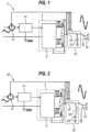
- Fig. 1illustrates an example of an audio pulse width modulation (PWM) amplifier 2.
- An audio PWM amplifieris a switching amplifier with a switching frequency usually in the region of 20 to 40 times higher than the highest audio frequency of the audio signal.
- the amplifierincludes a power stage 4.
- the power stage 4includes a gate driver or switching controller 6 which generates a signal comprising square pulses of fixed amplitude with a varying width and separation. It will be appreciated that the gate driver 6 generates a signal and an inverted and time delayed version of the same, the protective time delay is commonly known as dead-time.
- the amplifiercomprises block 14, which includes an integrator, comparator and switching frequency clock generator, with the clock typically in the form of a triangular or saw-tooth waveform.
- the low-frequency portion of the signal generated by block 14is the audio signal to be amplified and the high-frequency portion from the clock source which serves to create a PWM digital signal (i.e. a signal which switches between two distinct, predefined voltages) when combined with the low frequency audio signal.
- a PWM digital signali.e. a signal which switches between two distinct, predefined voltages
- the power stage 4includes two switching devices 8, 10.
- the output of the gate driver 6is coupled to the two switching devices in a push-pull or totem-pole arrangement.
- the switchesare field effect transistors (FET) 8, 10.
- FETfield effect transistors
- the upper FET 8is driven by the signal output by the driver 6 and the lower FET 10 is driven by the inverted and time delayed version of the same.
- the two switches 8, 10are arranged so as to be either fully on or fully off such that the output of the switching devices is at either +Vcc or-Vcc (i.e. the bus voltages). This type of arrangement utilises the property that if the push-pull output devices are either fully on or fully off they dissipate their minimum power leading to high amplifier efficiency.
- the output of the power stage 4is fed back to summation 12, whereby the input audio signal is summed with the output of the power stage 4.
- the summed signalis fed to block 14 to assist in compensating for variations in the output voltage with respect to the input voltage, due to finite and varying load configurations, and variations in bus voltage.
- the output of the power stage 4is filtered using a passive low pass filter 16 to filter out the switching frequency to allow a loudspeaker load 18 of the amplifier 2 to only see the audio signal.
- the standard and commonly used filter for the passive filter 16is a two-pole inductor-capacitor (LC) filter.
- the commonly used component values for the passive filter 16are a series inductor 20 of 20 ⁇ H and a capacitor 22 of 470nF shunted to ground.
- the loudspeaker 18may naturally filter out residual switching frequency energy conducted from the amplifier output with the audio signal. This residual energy may cause extra heat in the loudspeaker drive units, which may result in reduced linearity of the loudspeaker operation. This is undesirable.
- the passive filter 16provides an approximate voltage rejection of 35dB (1/56) at the switching frequency of the power amplifier output and may also be detrimental to the audio signal integrity causes 20 degrees of phase shift at 20kHz with an 8 ohm load, 36 degrees of phase shift at 20kHz with a 4 ohm load and 55 degrees of phase shift at 20kHz into a 2 ohm load.
- Loudspeaker impedance with respect to frequency curvesare not flat and the impedance may vary from 16 ohms at loudspeaker resonance/crossover to 3 ohms at DC due to the resistance of the voice coil. These standard component values cause audio material dependant vs loudspeaker dependant phase shifts in the audio which is noticeable to the discerning listener. Thus the quality of the audio and the listening experience is degraded.
- Reducing the series inductor 20 to 5 ⁇ Hmay reduce the phase shifts mentioned above by a factor of 4 with an 8 ohm load.
- the reductionbrings the loudspeaker phase-shift in line with the expectations of an analogue amplifier of around 5 degrees at 20kHz with an 8 ohm load.
- the sound quality from the amplifieris also brought in line with the expectations of an analogue amplifier.
- the series inductorshould not be typically reduced below 5 ⁇ H as this component limits/controls the peak current seen by the switching devices 8, 10.
- reducing the series inductoralso reduces the roll off achieved at the switching frequency of the amplifier, such that additional filtering is required to achieve a suitable level of attenuation of the switching frequency.
- EP 0 655 830 A1relates to a high-efficiency analog power amplifier.
- the amplifierutilizes pulse-width-modulation ("PWM") signals to operate electrical switching devices coupled in series across a d.c. power source.
- PWMpulse-width-modulation
- a resonant circuit coupled to the transistorsperiodically places zero and non-zero voltage levels across each transistor.
- the frequency and width of the PWM signalsare relative to the components of the resonant circuit, enabling each transistor to switch off and on only when zero volts appears across the transistor.
- the apparatusmay comprise a voltage follower arranged at the output of the filter arrangement.
- the output signalmay be a pulse width modulated signal, and may be an audio signal or a motor control signal.
- the modulated frequency componentmay be a triangular waveform.
- the circuit elementmay be a switching amplifier, and the switching amplifier may be a pulse width modulation amplifier.
- the circuit elementmay be a modulated carrier signal receiver, and the modulated frequency component is a carrier signal.
- Audiois a field that emphasizes in high integrity signal processing and reconstruction, due to the non-linear and high dynamic range and response of the human ear and its ability to detect phase shift and timing differences in sounds and music, especially when an audio signal passes through a filter or a circuit that has an altering effect on the signal phase information. Therefore, the apparatus described herein may be used for any application that requires high integrity signal reconstruction or recovery from a modulated signal that is sensitive to phase preservation.
- modulated frequency componentis used herein to describe a signal component which has been modulated when being combined with an information signal (e.g. an audio signal) in an amplifier (e.g. in an audio pulse width modulation (PWM) amplifier), or a carrier wave/component which has been modulated by an information signal for transmission.
- PWMpulse width modulation
- Fig. 2illustrates an audio circuit 30.
- the audio circuit 30is an audio pulse width modulation (PWM) amplifier.
- PWMpulse width modulation
- a PWM amplifieris a switching amplifier with a switching frequency typically in the region of 20 to 40 times higher than the highest audio frequency of an input audio signal.
- the audio circuit 30includes a power stage 4.
- the power stage 4includes a gate driver or switching controller 6 which generates a signal comprising square pulses of fixed amplitude with a varying width and separation. It will be appreciated that the gate driver generates a signal and an inverted and time delayed version of the same, to provide output device switching protection commonly referred to as dead-time.
- the low-frequency component of the signal generated by block 14is the audio signal to be amplified and the high-frequency component of the signal is typically a triangular or saw-tooth waveform which serves to create a digital signal (i.e.
- the high frequency componentis an out-of-band signal, or a signal to be modulated by the audio signal.
- the low frequency, audio signal and the high frequency, switching signalare combined using a comparator circuit.
- the power stage 4includes two switching devices 8, 10.
- the output of the gate driver 6is coupled to the two switching devices in a push-pull or totem-pole arrangement.
- the switchesare field effect transistors (FET) 8, 10.
- FETfield effect transistors
- the upper FET 8is driven by the signal output by the driver 6 and the lower FET 10 is driven by the inverted and time delayed version of the same.
- the two switches 8, 10are arranged so as to be either fully on or fully off such that the output of the switching devices is at either +Vcc or -Vcc (i.e. the bus voltages). This type of arrangement utilises the property that if the push-pull output devices are either fully on or fully off they dissipate their minimum power leading to high amplifier efficiency.
- Block 14includes an error amplifier or integrator, the output of which is coupled to a comparator which combines the audio signal output with a triangular or saw-tooth waveform generated by a signal generator, and the output of the comparator is fed to the power stage 4.
- the output of the power stage 4is filtered using a passive filter 32 to filter out the switching frequency to allow a loudspeaker load 18 of the audio circuit 30 to only see the audio signal.
- the passive filter 32comprises a series inductor 34 (5 ⁇ H), and a (series) shunt arrangement comprising a capacitor 38 (470nF) and an inductor 36 (337nH) shunted to ground. That is to say that the capacitor 38 and the inductor 36 are coupled in series and arranged at the signal output of the power stage 4, along with the series inductor 34.
- a loudspeaker 18is coupled to the series inductor 34 and ground with the shunt arrangement coupled in parallel with the loudspeaker 18.
- an inductoris added in series with the shunt capacitor and the resonance of these two components is exploited to create a notch in the filter response. Due to the large factor between the upper frequency of the passband and the design selected notch frequency this is achieved without adding additional phase shift to the audio signal.
- the passive filter arrangement 32can include the same component values as may be commonly used. However, it will be appreciated that these may be changed based on the desired response. For example, a series inductor (i.e. series inductor 34) of up to 20 ⁇ H may be used. Effectively, the components of a low pass filter are used in the filter arrangement, and the low pass filter is configured to attenuate the signal, in this example, at a frequency that is greater than the highest typical audio frequency (i.e. 20kHz) and less than the switching frequency (i.e. 400kHz in this example).
- the filter arrangementis configured to have a low phase shift of the order of 5 degrees, and in this example, around 5 degrees at 20kHz with an 8 ohm load is achieved.
- Lis the inductance of the shunt inductor 36
- Cis the capacitance of the shunt capacitor 38
- Fis equal to the switching frequency of the amplifier. It is appreciated that the switching frequency is equal to the frequency of the saw-tooth signal, for example, and may also be referred to as the modulated frequency component of the signal output by the power stage 4.
- L336.8nH ( i.e.
- Fig. 3illustrates the frequency response of the passive filter arrangement 32 illustrated in Fig. 2 .
- the upper graphillustrates gain in dB and the lower graph illustrates phase shift in degrees.
- the phase shift at 20kHzi.e. the upper frequency of the audio signal
- the phase shift at 20kHzis unchanged at 5 degrees when compared with the known passive filter 16 of Fig. 1 .
- the passive filteris not derived from k of the filter (i.e. the characteristic impedance), and that the passband/termination impedance, the slope of the roll-off or stopband attenuation are not of interest by the addition of this extra pole (i.e. the notch).
- the only design requirementis that the notch be in-line with the switching frequency of the power stage or the PWM modulated signal (i.e. a modulated frequency component or a carrier wave component).
- the modulated frequency componentmay also be referred to as a modulation frequency component.
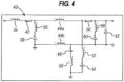
- Fig. 4illustrates a passive filter 40.
- the passive filter 40can be used as a replacement of the passive filter 32 illustrated in Fig. 2 .
- the series inductor 34, the shunt capacitor 38 and the shunt inductor 36 of the passive filter 40are the same as those illustrated in Fig. 2 .
- the passive filter 40includes three further filter configurations. In the first additional filter configuration an additional series inductor 44a, and a series shunt arrangement comprising an inductor 52 and a capacitor 54 are provided.
- the first additional filter configurationis coupled to the series inductor 34 via a resistor 42, which is added to dampen the reactive components. Resistor 42 may be omitted for high power outputs to avoid power loss.
- an additional series inductor 44b, and a shunt arrangement comprising a capacitor 48 and inductor 50are provided.
- the resonance effect created by capacitor 48 and inductor 50includes inductor 50 summed with inductor 44b, so with design optimisation of the capacitor 48 value inductor 50 may be omitted whilst still achieving the desired notch frequency Series inductors 44a and 44b form a common mode choke (i.e. inductors 44a and 44b are provided by a common mode choke in which the common mode currents in the inductors 44a and 44b flow in the same direction through each of the choke/inductor windings).
- the second additional filter configurationis coupled to the ground connection of the capacitor 38.
- an additional series shunt arrangementcomprising an inductor 58 and a capacitor 60 are added.
- the third additional filter configurationis added on the loudspeaker side of the filter, and is coupled to the inductor 44a of the first additional filter configuration and the inductor 44b of the second additional filter configuration.
- the third additional filter configurationis coupled to the inductor 44a of the first additional filter configuration via a resistor 56, which is added to dampen the reactive components. Resistor 56 may be omitted for high power outputs to avoid power loss.
- a capacitor 62is also added across the loudspeaker load to control EMC at VHF.
- further inductorsbetween the first filter stage (i.e. the series inductor 34, the shunt capacitor 38 and the shunt inductor 36) and the loudspeaker (i.e. inductors 44a and 52) and also the ground return (i.e. inductor 44b), and capacitors on the loudspeaker side of the inductors (i.e. capacitors 48, 54, 60 and 62), further stages of filtering, for example 3, can be cascaded which causes little further audio signal phase shift at 20kHz but adds a further 3 sets of independently tuned resonances that can be used on an application specific basis to notch out harmonics of the switching frequency fundamental.
- the common mode choke 44a and 44bis selected so that the phase shift at 20kHz is within desired limits for the operational load impedance. For a 1 ⁇ H series inductor (i.e. inductors 44a and 44b) the phase shift is limited to 7.2 degrees at 20kHz into the 8 ohm operational load.
- shunt inductors 52 and 58 for a switching frequency of 400kHzare selected to be 720nH.
- a single LC notch filtercan provide an additional 40dB attenuation to a passive LC low pass filter configuration at a design selected frequency such as 400kHz. If a further three LC filters of identical values are added in parallel, the first addition gives a further 6dB attenuation, the second gives a further 4dB attenuation, the third gives a further 2dB attenuation, totalling 74dB.
- the passive filter described in association with Fig. 4allows up to a total of four LC notch filters (i.e. three could be used) to be used in a passive high-power filter network and achieve a theoretical 220dB attenuation with minimal in-band signal phase shift.
- the ability to preserve phaseis by use of a common mode choke, and its inherent property to preserve signal integrity by the action of the forward signal path field and the return signal path field to cancel, which minimises the inductance presented to a forward path current that exactly matches the return path current, such as the signal.
- a further three LC notch filtersare added to the load side of the common mode choke series inductances, and the resonances are selected to combine with differing and particular portions of the common mode choke inductances, with the across line and ground (commonly referred with use of common mode choke applications as X and Y) capacitances, the exceptionally high level of passive filter attenuation can be achieved by the selectively combined interaction of the phase lag (inductive) and phase lead (capacitive) reactances.
- Fig. 5illustrates the frequency response of the passive filter arrangement 40 illustrated in Fig. 4 .
- the upper graphillustrates gain in dB and the lower graph illustrates phase in degrees.
- there is a notch in the frequency response at 400kHzi.e. 20 times the upper frequency of the audio signal of 20kHz
- the phase shift at 20kHzi.e. the upper frequency of the audio signal
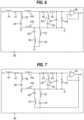
- Fig. 6illustrates an active filter arrangement 80 as used in examplary embodiment according to the invention.
- the active filter arrangement 80could be used for low power and line level filtering.
- the active filter arrangement 80includes all the same component's illustrated in Fig. 4 with the addition of a voltage follower 66 (i.e. an operational amplifier with its output coupled to its inverting input).
- a shunt resistor 64is provided having a value of 10k ohms, for example, to place less loading on the filter components.
- An additional series resistor 68is also provided having a value of 1 to 10 ohms if required.
- the shunt resistor 64reduces the required power rating of the filter components but also reduces the damping of the filter.
- resistors 64 and 68may be omitted. Indeed, resistors 42, 56, 64 and 68 are selected to control the damping of high Q inductors and capacitors, and can all be omitted if low Q parts are used.
- Fig. 7illustrates a further active filter arrangement 90 as used in examplary embodiment according to the invention.
- the active filter arrangement 90includes all the same components illustrated in Fig. 6 , except the inductor 50 and the capacitor 54 are coupled to the output of the voltage follower 70.
- the filter arrangements depicted in Fig. 6 and Fig 7have very close in-band responses, and the filter arrangement depicted in Fig. 6 has an in-band phase improvement of 2 degrees. However, the filter arrangement depicted in Fig. 6 has an out-of-band response that is dependent on operational amplifier characteristics whereas the filter arrangement depicted in Fig. 7 response is controlled entirely by the passive components.
- the filter arrangements depicted in Fig. 6 and Fig 7may be followed by an operational amplifier gain stage to adjust the Q/width of the filter.
- Each of the inductors mentioned hereinmay be implemented as a wound inductor or magnetic device, in PCB trace/track, as an electronic circuit that produces inductance by means of phase shift control.
- Figs. 2 and 4are pulse width modulation or PWM circuit arrangements.
- the filter arrangements described in association with Figs. 2 , 4 , 6 and 7could be used in a pulse density modulation circuit or a circuit arrangement whereby a digital bit stream (e.g. direct stream digital, super audio compact disc, and line level signals) is used to switch an FET transistor, or a communication receiver circuit involving the use of a signal (analogue or digital) modulated by a carrier wave, for example.
- the filter arrangements described hereinmay be used with any circuit arrangement which use a switching arrangement similar to the one illustrated in Fig. 2 or a system utilizing a modulated carrier wave signal.
- the filter arrangements described in association with Figs. 2 , and 4could be used in the circuit arrangement 202 illustrated in Fig. 8 .
- the circuit arrangement 202is a motor controller and includes a power stage 204, which is fed by Block 214.
- Block 214includes an integrator, comparator and switching frequency clock generator, with the clock typically in the form of a triangular or saw-tooth waveform.
- the power stage 204includes a gate driver or switching controller 206 which generates a signal comprising square pulses of fixed amplitude with a varying width and separation. It will be appreciated that the gate driver generates a signal and an inverted and time delayed version of the same.
- the power stage 204includes two switching devices 208, 210.
- the output of the gate driver 206is coupled to the two switching devices in a push-pull or totem-pole arrangement.
- the switchesare field effect transistors (FET) 208, 210.
- FETfield effect transistors
- the upper FET 208is driven by the signal output by the driver 206 and the lower FET 210 is driven by the inverted and time delayed version of the same.
- the two switches 208, 210are arranged so as to be either fully on or fully off such that the output of the switching devices is at either +Vcc or -Vcc (i.e. the bus voltages). This type of arrangement utilises the property that if the push-pull output devices are either fully on or fully off they dissipate their minimum power leading to high amplifier efficiency.
- the output of the power stage 204is fed back to summation 212, whereby the input audio signal is summed with the output of the power stage 204.
- the summed signalis fed to block 214 to assist in compensating for variations in the output voltage with respect to the input voltage, due to finite and varying load configurations, and variations in bus voltage.
- the output of the power stage 204is filtered using a filter arrangement 216 to filter out the switching frequency to allow a motor 218 of the circuit 202 to only see a motor control signal.
- the filter arrangement 216may be one of the filter arrangements described in association with Figs. 2 and 4 for high power conditions.
- the filter arrangements described in association with Figs. 6 and 7could be used in the circuit arrangement illustrated in Fig. 9 .
- the circuit arrangementassists in the conversion of a low power PWM source, for example, into a low power analogue waveform, in order to be processed, amplified or transduced by an analogue mechanism.
- a low power PWM source 222or a bit-stream or DSD source
- DACDigital-to-Analogue Converter
- DACDigital-to-Analogue Converter
- the filter arrangement 238may be one of the filter arrangements described in association with Figs. 6 and 7 .
- the output of the filter arrangement 238is coupled to an analogue amplifier or a digital amplifier 240, which drives the load 242.
- the load 242 in this exampleis a loudspeaker.
- the active configuration illustrated in Fig. 9may be used in low power conditions such as line level.
- Fig. 10is a system block diagram illustrating an electromagnetic transmission carrier signal (e.g. RF) recovery application.
- a modulated carrier receiver 244as is known in the art (e.g. an antenna coupled to a preamplifier and amplifier).
- the receiver 244is coupled to a filter arrangement 246, which is tuned to remove the carrier component/signal (or the modulated frequency component) from the received signal.
- the filter arrangement 246may be one of the filter arrangements described in association with Figs. 2 , 4 , 6 and 7 .
- the output of the filter arrangement 246is coupled to a post processing block 248 dependent on the application.
- the received signalmight be a modulated audio signal and the post processing block is an audio amplifier driving a loudspeaker.
- the system illustrated in Fig. 10might be a digital or analogue topology.
- Fig. 11is a system block diagram illustrating an electromagnetic transmission carrier signal (e.g. optical) recovery application.
- an optical detection device 252coupled to a modulated carrier receiver 250 (e.g. transimpedance and voltage gain amplifiers) as is known in the art.
- the receiver 250is coupled to a filter arrangement 254, which is tuned to remove the carrier wave/component (or the modulated frequency component) of the received signal.
- the filter arrangement 254may be one of the filter arrangements described in association with Figs. 2 , 4 , 6 and 7 .
- the output of the filter arrangement 254is coupled to a post processing block 256 dependent on the application.
- the system illustrated in Fig. 11might be a digital or analogue topology.
Landscapes
- Engineering & Computer Science (AREA)
- Power Engineering (AREA)
- Physics & Mathematics (AREA)
- Acoustics & Sound (AREA)
- Signal Processing (AREA)
- Multimedia (AREA)
- Amplifiers (AREA)
- Sink And Installation For Waste Water (AREA)
- Filtering Of Dispersed Particles In Gases (AREA)
Description
- The invention relates to an electronic filter apparatus. In particular, the invention relates to an electronic apparatus comprising a circuit element, such as a switching amplifier, configured to output a signal comprising a modulated frequency component and cascaded notch filter arrangements. The signal has phase information that is sensitive to alteration, such as audio.
Fig. 1 illustrates an example of an audio pulse width modulation (PWM)amplifier 2. An audio PWM amplifier is a switching amplifier with a switching frequency usually in the region of 20 to 40 times higher than the highest audio frequency of the audio signal. The amplifier includes a power stage 4. The power stage 4 includes a gate driver orswitching controller 6 which generates a signal comprising square pulses of fixed amplitude with a varying width and separation. It will be appreciated that thegate driver 6 generates a signal and an inverted and time delayed version of the same, the protective time delay is commonly known as dead-time. The amplifier comprisesblock 14, which includes an integrator, comparator and switching frequency clock generator, with the clock typically in the form of a triangular or saw-tooth waveform. The low-frequency portion of the signal generated byblock 14 is the audio signal to be amplified and the high-frequency portion from the clock source which serves to create a PWM digital signal (i.e. a signal which switches between two distinct, predefined voltages) when combined with the low frequency audio signal.- The power stage 4 includes two
switching devices gate driver 6 is coupled to the two switching devices in a push-pull or totem-pole arrangement. In the circuit illustrated inFig. 1 , the switches are field effect transistors (FET) 8, 10. In the figure, theupper FET 8 is driven by the signal output by thedriver 6 and thelower FET 10 is driven by the inverted and time delayed version of the same. The twoswitches summation 12, whereby the input audio signal is summed with the output of the power stage 4. The summed signal is fed to block 14 to assist in compensating for variations in the output voltage with respect to the input voltage, due to finite and varying load configurations, and variations in bus voltage. - The output of the power stage 4 is filtered using a passive
low pass filter 16 to filter out the switching frequency to allow aloudspeaker load 18 of theamplifier 2 to only see the audio signal. The standard and commonly used filter for thepassive filter 16 is a two-pole inductor-capacitor (LC) filter. The commonly used component values for thepassive filter 16 are aseries inductor 20 of 20µH and acapacitor 22 of 470nF shunted to ground. Theloudspeaker 18 may naturally filter out residual switching frequency energy conducted from the amplifier output with the audio signal. This residual energy may cause extra heat in the loudspeaker drive units, which may result in reduced linearity of the loudspeaker operation. This is undesirable. - The
passive filter 16 provides an approximate voltage rejection of 35dB (1/56) at the switching frequency of the power amplifier output and may also be detrimental to the audio signal integrity causes 20 degrees of phase shift at 20kHz with an 8 ohm load, 36 degrees of phase shift at 20kHz with a 4 ohm load and 55 degrees of phase shift at 20kHz into a 2 ohm load. Loudspeaker impedance with respect to frequency curves are not flat and the impedance may vary from 16 ohms at loudspeaker resonance/crossover to 3 ohms at DC due to the resistance of the voice coil. These standard component values cause audio material dependant vs loudspeaker dependant phase shifts in the audio which is noticeable to the discerning listener. Thus the quality of the audio and the listening experience is degraded. - Reducing the
series inductor 20 to 5µH may reduce the phase shifts mentioned above by a factor of 4 with an 8 ohm load. The reduction brings the loudspeaker phase-shift in line with the expectations of an analogue amplifier of around 5 degrees at 20kHz with an 8 ohm load. The sound quality from the amplifier is also brought in line with the expectations of an analogue amplifier. It is noted that the series inductor should not be typically reduced below 5µH as this component limits/controls the peak current seen by theswitching devices - In this regard, it is widely accepted within the field of audio that high definition audio of 16 bits or higher demands a noise floor that is more than 90dB below the full-scale signal, to be below the perception of the discerning listener. Therefore, it would be desirable to provide a circuit which meets the expectations of phase-shift and sound quality of an analogue amplifier using a PWM amplifier, for example, while achieving a suitable level of attenuation of the switching frequency.
EP 0 655 830 A1 relates to a high-efficiency analog power amplifier. The amplifier utilizes pulse-width-modulation ("PWM") signals to operate electrical switching devices coupled in series across a d.c. power source. A resonant circuit coupled to the transistors periodically places zero and non-zero voltage levels across each transistor. The frequency and width of the PWM signals are relative to the components of the resonant circuit, enabling each transistor to switch off and on only when zero volts appears across the transistor.- The present disclosure can be understood with reference to the description of the embodiments set out below, in conjunction with the appended drawings in which:
Fig. 1 , described above, illustrates an example of an audio pulse width modulation (PWM) amplifier;Fig. 2 illustrates an audio circuit;Fig. 3 illustrates a frequency response of a passive filter illustrated inFig. 2 ;Fig. 4 illustrates a passive filter;Fig. 5 illustrates a frequency response of the passive filter illustrated inFig. 4 ;Fig. 6 illustrates an active filter arrangement;Fig. 7 illustrates a further active filter arrangement;Fig. 8 is a motor controller which can be used with the filter arrangements described in association withFigs. 2 and4 ;Fig. 9 is a system block diagram which can be used with the filter arrangements described in association withFigs. 6 and 7 ;Fig. 10 is a system block diagram illustrating an electromagnetic transmission carrier signal (e.g. RF) recovery application; andFig. 11 is a system block diagram illustrating an electromagnetic transmission carrier signal (e.g. optical) recovery application.- According to a first embodiment of the invention there is provided an electronic apparatus according to
claim 1. - The apparatus may comprise a voltage follower arranged at the output of the filter arrangement.
- The output signal may be a pulse width modulated signal, and may be an audio signal or a motor control signal.
- The modulated frequency component may be a triangular waveform.
- The circuit element may be a switching amplifier, and the switching amplifier may be a pulse width modulation amplifier.
- The circuit element may be a modulated carrier signal receiver, and the modulated frequency component is a carrier signal.
- Audio is a field that specialises in high integrity signal processing and reconstruction, due to the non-linear and high dynamic range and response of the human ear and its ability to detect phase shift and timing differences in sounds and music, especially when an audio signal passes through a filter or a circuit that has an altering effect on the signal phase information. Therefore, the apparatus described herein may be used for any application that requires high integrity signal reconstruction or recovery from a modulated signal that is sensitive to phase preservation. The phrase modulated frequency component is used herein to describe a signal component which has been modulated when being combined with an information signal (e.g. an audio signal) in an amplifier (e.g. in an audio pulse width modulation (PWM) amplifier), or a carrier wave/component which has been modulated by an information signal for transmission.
Fig. 2 illustrates anaudio circuit 30. Theaudio circuit 30 is an audio pulse width modulation (PWM) amplifier.- A PWM amplifier is a switching amplifier with a switching frequency typically in the region of 20 to 40 times higher than the highest audio frequency of an input audio signal. The
audio circuit 30 includes a power stage 4. The power stage 4 includes a gate driver or switchingcontroller 6 which generates a signal comprising square pulses of fixed amplitude with a varying width and separation. It will be appreciated that the gate driver generates a signal and an inverted and time delayed version of the same, to provide output device switching protection commonly referred to as dead-time. The low-frequency component of the signal generated byblock 14 is the audio signal to be amplified and the high-frequency component of the signal is typically a triangular or saw-tooth waveform which serves to create a digital signal (i.e. a signal which switches between two distinct, predefined voltages) when combined with the low frequency audio signal. The high frequency component is an out-of-band signal, or a signal to be modulated by the audio signal. As is known in the art, the low frequency, audio signal and the high frequency, switching signal (i.e. out-of-band signal) are combined using a comparator circuit. - The power stage 4 includes two
switching devices gate driver 6 is coupled to the two switching devices in a push-pull or totem-pole arrangement. In the circuit illustrated inFig. 2 , the switches are field effect transistors (FET) 8, 10. In the figure, theupper FET 8 is driven by the signal output by thedriver 6 and thelower FET 10 is driven by the inverted and time delayed version of the same. The twoswitches summation 12, whereby the input audio signal is summed with the output of the power stage 4. The summed signal is fed to block 14 to assist in compensating for variations in the output voltage with respect to the input voltage, due to finite and varying load configurations, and variations in bus voltage.Block 14 includes an error amplifier or integrator, the output of which is coupled to a comparator which combines the audio signal output with a triangular or saw-tooth waveform generated by a signal generator, and the output of the comparator is fed to the power stage 4. - The output of the power stage 4 is filtered using a
passive filter 32 to filter out the switching frequency to allow aloudspeaker load 18 of theaudio circuit 30 to only see the audio signal. - The
passive filter 32 comprises a series inductor 34 (5µH), and a (series) shunt arrangement comprising a capacitor 38 (470nF) and an inductor 36 (337nH) shunted to ground. That is to say that thecapacitor 38 and theinductor 36 are coupled in series and arranged at the signal output of the power stage 4, along with theseries inductor 34. Aloudspeaker 18 is coupled to theseries inductor 34 and ground with the shunt arrangement coupled in parallel with theloudspeaker 18. In comparison with thepassive filter 16 ofFig. 1 , an inductor is added in series with the shunt capacitor and the resonance of these two components is exploited to create a notch in the filter response. Due to the large factor between the upper frequency of the passband and the design selected notch frequency this is achieved without adding additional phase shift to the audio signal. - The
passive filter arrangement 32 can include the same component values as may be commonly used. However, it will be appreciated that these may be changed based on the desired response. For example, a series inductor (i.e. series inductor 34) of up to 20µH may be used. Effectively, the components of a low pass filter are used in the filter arrangement, and the low pass filter is configured to attenuate the signal, in this example, at a frequency that is greater than the highest typical audio frequency (i.e. 20kHz) and less than the switching frequency (i.e. 400kHz in this example). As described above with the series inductor 34 (5µH), in addition to the cut-off frequency of thefilter arrangement 32, the filter arrangement is configured to have a low phase shift of the order of 5 degrees, and in this example, around 5 degrees at 20kHz with an 8 ohm load is achieved. - The
shunt capacitor 38 and theshunt inductor 36 are selected to have high Q factor (i.e. a low internal resistance), and to satisfy the expressionF =1/2π√(L*C). In this expression,L is the inductance of theshunt inductor 36,C is the capacitance of theshunt capacitor 38, andF is equal to the switching frequency of the amplifier. It is appreciated that the switching frequency is equal to the frequency of the saw-tooth signal, for example, and may also be referred to as the modulated frequency component of the signal output by the power stage 4. In thepassive filter 32 ofFig. 2 , usingL =336.8nH (i.e. L =1/((2π xF)2 xC)) a further 33.6dB rejection is achieved, totalling 61.9dB at the switching frequency of 400kHz. These values have been calculated using a loudspeaker with an 8 ohm load. Fig. 3 illustrates the frequency response of thepassive filter arrangement 32 illustrated inFig. 2 . The upper graph illustrates gain in dB and the lower graph illustrates phase shift in degrees. As can be seen fromFig. 3 , there is a notch in the frequency response at 400kHz (i.e. 20 times the upper frequency of the audio signal of 20kHz), which is the switching frequency (i.e. the frequency of the modulated component) of the power stage 4. Furthermore, the phase shift at 20kHz (i.e. the upper frequency of the audio signal) is unchanged at 5 degrees when compared with the knownpassive filter 16 ofFig. 1 .- It is noted that the passive filter is not derived from k of the filter (i.e. the characteristic impedance), and that the passband/termination impedance, the slope of the roll-off or stopband attenuation are not of interest by the addition of this extra pole (i.e. the notch). The only design requirement is that the notch be in-line with the switching frequency of the power stage or the PWM modulated signal (i.e. a modulated frequency component or a carrier wave component). The modulated frequency component may also be referred to as a modulation frequency component.
Fig. 4 illustrates apassive filter 40. Thepassive filter 40 can be used as a replacement of thepassive filter 32 illustrated inFig. 2 . Theseries inductor 34, theshunt capacitor 38 and theshunt inductor 36 of thepassive filter 40 are the same as those illustrated inFig. 2 . Thepassive filter 40 includes three further filter configurations. In the first additional filter configuration anadditional series inductor 44a, and a series shunt arrangement comprising aninductor 52 and acapacitor 54 are provided. The first additional filter configuration is coupled to theseries inductor 34 via aresistor 42, which is added to dampen the reactive components.Resistor 42 may be omitted for high power outputs to avoid power loss. In the second additional filter configuration anadditional series inductor 44b, and a shunt arrangement comprising acapacitor 48 andinductor 50 are provided. Notably, the resonance effect created bycapacitor 48 andinductor 50 includesinductor 50 summed withinductor 44b, so with design optimisation of thecapacitor 48value inductor 50 may be omitted whilst still achieving the desired notchfrequency Series inductors inductors capacitor 38. In the third additional filter configuration an additional series shunt arrangement comprising aninductor 58 and acapacitor 60 are added. The third additional filter configuration is added on the loudspeaker side of the filter, and is coupled to theinductor 44a of the first additional filter configuration and theinductor 44b of the second additional filter configuration. The third additional filter configuration is coupled to theinductor 44a of the first additional filter configuration via aresistor 56, which is added to dampen the reactive components.Resistor 56 may be omitted for high power outputs to avoid power loss. Acapacitor 62 is also added across the loudspeaker load to control EMC at VHF.- By adding further inductors between the first filter stage (i.e. the
series inductor 34, theshunt capacitor 38 and the shunt inductor 36) and the loudspeaker (i.e. inductors 44a and 52) and also the ground return (i.e. inductor 44b), and capacitors on the loudspeaker side of the inductors (i.e.capacitors - The capacitance values for
shunt capacitors capacitors 54 and 60) based on Xc = 1/(2π x F x C). - The
common mode choke - The
shunt network inductors shunt inductors - If
inductor 50 is omitted then shuntcapacitor 48 creates a resonant tank withseries inductor 44b andshunt capacitor 48 value is calculated C = 1/((2π x F)2 x L), where F is chosen as the switching frequency and L is the inductance ofseries inductor 44b. Using these values and a switching frequency of400kHz shunt capacitor 48 would be theoretically 158.3nF. - If
inductor 50 is included and an arbitrary value of 100nH is used, the calculated capacitance C = 1/((2π x F)2 x L), where L =inductance 44b +inductance 50.Inductor 50 may be added to the circuit to provide greater control or selectivity over the frequency being notched, vs the capacitance value forcapacitor 48. - As detailed above a single LC notch filter can provide an additional 40dB attenuation to a passive LC low pass filter configuration at a design selected frequency such as 400kHz. If a further three LC filters of identical values are added in parallel, the first addition gives a further 6dB attenuation, the second gives a further 4dB attenuation, the third gives a further 2dB attenuation, totalling 74dB. The passive filter described in association with
Fig. 4 allows up to a total of four LC notch filters (i.e. three could be used) to be used in a passive high-power filter network and achieve a theoretical 220dB attenuation with minimal in-band signal phase shift. The ability to preserve phase is by use of a common mode choke, and its inherent property to preserve signal integrity by the action of the forward signal path field and the return signal path field to cancel, which minimises the inductance presented to a forward path current that exactly matches the return path current, such as the signal. When a further three LC notch filters are added to the load side of the common mode choke series inductances, and the resonances are selected to combine with differing and particular portions of the common mode choke inductances, with the across line and ground (commonly referred with use of common mode choke applications as X and Y) capacitances, the exceptionally high level of passive filter attenuation can be achieved by the selectively combined interaction of the phase lag (inductive) and phase lead (capacitive) reactances. Fig. 5 illustrates the frequency response of thepassive filter arrangement 40 illustrated inFig. 4 . The upper graph illustrates gain in dB and the lower graph illustrates phase in degrees. As can be seen fromFig. 5 , there is a notch in the frequency response at 400kHz (i.e. 20 times the upper frequency of the audio signal of 20kHz), which is the switching frequency of the power stage and gives a total 220.0dB theoretical rejection at the switching frequency. Furthermore, the phase shift at 20kHz (i.e. the upper frequency of the audio signal) is 7.6 degrees with an 8 ohm load.Fig. 6 illustrates anactive filter arrangement 80 as used in examplary embodiment according to the invention. Theactive filter arrangement 80 could be used for low power and line level filtering. Theactive filter arrangement 80 includes all the same component's illustrated inFig. 4 with the addition of a voltage follower 66 (i.e. an operational amplifier with its output coupled to its inverting input). Ashunt resistor 64 is provided having a value of 10k ohms, for example, to place less loading on the filter components. Anadditional series resistor 68 is also provided having a value of 1 to 10 ohms if required. Theshunt resistor 64 reduces the required power rating of the filter components but also reduces the damping of the filter. Accordingly additional series resistors can be added to control the circuit to have the same response as is illustrated inFig. 5 . Furthermore,resistors resistors Fig. 7 illustrates a furtheractive filter arrangement 90 as used in examplary embodiment according to the invention. Theactive filter arrangement 90 includes all the same components illustrated inFig. 6 , except theinductor 50 and thecapacitor 54 are coupled to the output of thevoltage follower 70.- The filter arrangements depicted in
Fig. 6 and Fig 7 have very close in-band responses, and the filter arrangement depicted inFig. 6 has an in-band phase improvement of 2 degrees. However, the filter arrangement depicted inFig. 6 has an out-of-band response that is dependent on operational amplifier characteristics whereas the filter arrangement depicted inFig. 7 response is controlled entirely by the passive components. The filter arrangements depicted inFig. 6 and Fig 7 may be followed by an operational amplifier gain stage to adjust the Q/width of the filter. - Each of the inductors mentioned herein may be implemented as a wound inductor or magnetic device, in PCB trace/track, as an electronic circuit that produces inductance by means of phase shift control.
- The examples described with respect to
Figs. 2 and4 are pulse width modulation or PWM circuit arrangements. However, it will be appreciated that the filter arrangements described in association withFigs. 2 ,4 ,6 and 7 could be used in a pulse density modulation circuit or a circuit arrangement whereby a digital bit stream (e.g. direct stream digital, super audio compact disc, and line level signals) is used to switch an FET transistor, or a communication receiver circuit involving the use of a signal (analogue or digital) modulated by a carrier wave, for example. In other words, the filter arrangements described herein may be used with any circuit arrangement which use a switching arrangement similar to the one illustrated inFig. 2 or a system utilizing a modulated carrier wave signal. - For example, the filter arrangements described in association with
Figs. 2 , and4 could be used in thecircuit arrangement 202 illustrated inFig. 8 . Thecircuit arrangement 202 is a motor controller and includes apower stage 204, which is fed byBlock 214.Block 214 includes an integrator, comparator and switching frequency clock generator, with the clock typically in the form of a triangular or saw-tooth waveform. Thepower stage 204 includes a gate driver or switchingcontroller 206 which generates a signal comprising square pulses of fixed amplitude with a varying width and separation. It will be appreciated that the gate driver generates a signal and an inverted and time delayed version of the same. Thepower stage 204 includes twoswitching devices gate driver 206 is coupled to the two switching devices in a push-pull or totem-pole arrangement. In the circuit illustrated inFig. 8 , the switches are field effect transistors (FET) 208, 210. In the figure, theupper FET 208 is driven by the signal output by thedriver 206 and thelower FET 210 is driven by the inverted and time delayed version of the same. The twoswitches power stage 204 is fed back tosummation 212, whereby the input audio signal is summed with the output of thepower stage 204. The summed signal is fed to block 214 to assist in compensating for variations in the output voltage with respect to the input voltage, due to finite and varying load configurations, and variations in bus voltage. - The output of the
power stage 204 is filtered using afilter arrangement 216 to filter out the switching frequency to allow amotor 218 of thecircuit 202 to only see a motor control signal. Thefilter arrangement 216 may be one of the filter arrangements described in association withFigs. 2 and4 for high power conditions. - In a further example, the filter arrangements described in association with
Figs. 6 and 7 could be used in the circuit arrangement illustrated inFig. 9 . The circuit arrangement assists in the conversion of a low power PWM source, for example, into a low power analogue waveform, in order to be processed, amplified or transduced by an analogue mechanism. In the circuit arrangement ofFig. 9 there is provided a low power PWM source 222 (or a bit-stream or DSD source) coupled to a Digital-to-Analogue Converter (DAC) 236 that uses a fixed switching frequency (e.g. a Direct Stream Digital or DSD DAC) which is coupled to afilter arrangement 238 to filter out the switching frequency of the lowpower PWM source 222. Thefilter arrangement 238 may be one of the filter arrangements described in association withFigs. 6 and 7 . The output of thefilter arrangement 238 is coupled to an analogue amplifier or adigital amplifier 240, which drives theload 242. Theload 242 in this example is a loudspeaker. The active configuration illustrated inFig. 9 may be used in low power conditions such as line level. Fig. 10 is a system block diagram illustrating an electromagnetic transmission carrier signal (e.g. RF) recovery application. In the system illustrated inFig. 10 , there is provided a modulatedcarrier receiver 244 as is known in the art (e.g. an antenna coupled to a preamplifier and amplifier). Thereceiver 244 is coupled to afilter arrangement 246, which is tuned to remove the carrier component/signal (or the modulated frequency component) from the received signal. Thefilter arrangement 246 may be one of the filter arrangements described in association withFigs. 2 ,4 ,6 and 7 . The output of thefilter arrangement 246 is coupled to a post processing block 248 dependent on the application. For example, the received signal might be a modulated audio signal and the post processing block is an audio amplifier driving a loudspeaker. The system illustrated inFig. 10 might be a digital or analogue topology.Fig. 11 is a system block diagram illustrating an electromagnetic transmission carrier signal (e.g. optical) recovery application. In the system illustrated inFig. 11 , there is provided an optical detection device 252 coupled to a modulated carrier receiver 250 (e.g. transimpedance and voltage gain amplifiers) as is known in the art. Thereceiver 250 is coupled to afilter arrangement 254, which is tuned to remove the carrier wave/component (or the modulated frequency component) of the received signal. Thefilter arrangement 254 may be one of the filter arrangements described in association withFigs. 2 ,4 ,6 and 7 . The output of thefilter arrangement 254 is coupled to a post processing block 256 dependent on the application. The system illustrated inFig. 11 might be a digital or analogue topology.- Any quoted attenuation figures are from simulation and have utilised accurate RF models incorporating parasitic components where applicable, therefore, carefully selected components may be close to, but may not necessarily match, the simulated performance.
- It will be appreciated that the foregoing discussion relates to particular embodiments. However, in other embodiments, various aspects and examples may be combined.
Claims (8)
- An electronic apparatus comprising:a circuit element configured to receive an in-band low-frequency input signal and to output a pulse-width modulated, PWM, output signal that is generated by modulating a high-frequency out-of-band signal using the low-frequency input signal, the circuit suitable to perform a PWM modulation of the high-frequency out-of-band signal and comprising:a filter arrangement (40) comprising a notch filter arrangement, and first and second additional notch filter arrangements,wherein the notch filter arrangement comprises a first series inductor (34) coupled with its one end to the output of the circuit element, and a first series shunt configuration coupled with its one end to the other end of the first series inductor and with its other end to the ground, the first series shunt configuration comprising a second inductor (36) and a first capacitor (38) coupled in series,wherein the first additional notch filter arrangement comprises a third series inductor (44a) coupled with its one end to the one end of the first series shunt configuration, and a second series shunt configuration coupled with its one end to the other end of the third series inductor and with its other end to the ground, the second series shunt configuration comprising a fourth inductor (52) and a second capacitor (54) coupled in series,wherein the second additional notch filter arrangement comprises a fifth series inductor (44b) coupled with its one end to the ground and a shunt capacitor (48) coupled with its one end to the other end of the fifth series inductor and with its other end to the ground, andwherein each of the notch filter arrangements are configured to generate a notch in a frequency response to attenuate the output signal at a frequency of the high-frequency out-of-band signal;wherein the filter arrangement (40) comprises a third additional notch filter arrangement coupled with its one end to the the other end of the third series inductor (44a) and its other end to the other end of the fifth series inductor (44b), the third additional notch filter arrangement comprising a sixth inductor (58) and a third capacitor (60) coupled in series, wherein the third series inductor (44a) of the first additional notch filter arrangement and the fifth series inductor (44b) of the second additional notch filter arrangement form a common mode choke that is selected so that the phase shift at an upper frequency of the low-frequency input signal is within desired limits for an operational load impedance of a load of the filter arrangement (40) that is coupled in parallel to the third additional notch filter arrangement.
- The apparatus of claim 1, comprising a voltage follower arranged at the output of the filter arrangement.
- The apparatus of any preceding claim, wherein the output signal is a pulse width modulated signal.
- The apparatus of any preceding claim, wherein the output signal is an audio signal or a motor control signal.
- The apparatus of any preceding claim, wherein the the high-frequency out-of-band signal is a triangular waveform.
- The apparatus of any preceding claim, wherein the circuit element is a switching amplifier.
- The apparatus of claim 6, wherein the switching amplifier is a pulse width modulation amplifier.
- The apparatus of any one of claims 1 to 5, wherein the circuit element is a modulated carrier signal receiver, and the high-frequency out-of-band signal is a carrier signal.
Applications Claiming Priority (2)
| Application Number | Priority Date | Filing Date | Title |
|---|---|---|---|
| GB1803569.1AGB2571732A (en) | 2018-03-06 | 2018-03-06 | An apparatus |
| PCT/GB2019/050633WO2019171059A1 (en) | 2018-03-06 | 2019-03-06 | An electronic filter apparatus |
Publications (2)
| Publication Number | Publication Date |
|---|---|
| EP3776849A1 EP3776849A1 (en) | 2021-02-17 |
| EP3776849B1true EP3776849B1 (en) | 2023-06-07 |
Family
ID=61903693
Family Applications (1)
| Application Number | Title | Priority Date | Filing Date |
|---|---|---|---|
| EP19718908.7AActiveEP3776849B1 (en) | 2018-03-06 | 2019-03-06 | An electronic filter apparatus |
Country Status (5)
| Country | Link |
|---|---|
| US (1) | US11476821B2 (en) |
| EP (1) | EP3776849B1 (en) |
| GB (1) | GB2571732A (en) |
| TW (1) | TWI806979B (en) |
| WO (1) | WO2019171059A1 (en) |
Families Citing this family (1)
| Publication number | Priority date | Publication date | Assignee | Title |
|---|---|---|---|---|
| US11984820B2 (en)* | 2020-10-30 | 2024-05-14 | Cummins Power Generation Inc. | Systems and methods for increasing efficiency of a power converter |
Citations (3)
| Publication number | Priority date | Publication date | Assignee | Title |
|---|---|---|---|---|
| EP0655830A1 (en)* | 1993-11-30 | 1995-05-31 | Kaiser Aerospace And Electronics Corporation | Very low power loss amplifier for analog signals utilizing constant-frequency zero-voltage-switchting multi-resonant converter |
| US7596006B1 (en)* | 2006-08-09 | 2009-09-29 | Lockheed Martin Corporation | Reducing output ripple from a switched mode power converter |
| US20170207795A1 (en)* | 2016-01-15 | 2017-07-20 | Texas Instruments Incorporated | Digital to analog converter with passive reconstruction filter |
Family Cites Families (11)
| Publication number | Priority date | Publication date | Assignee | Title |
|---|---|---|---|---|
| FR2166696A5 (en)* | 1972-01-04 | 1973-08-17 | Ass Ouvriers Instr Preci | |
| JPS59814Y2 (en)* | 1977-04-22 | 1984-01-11 | ブライアン・ア−ネスト・アトウツド | class D amplifier |
| IL72925A0 (en)* | 1983-10-07 | 1984-12-31 | Sundstrand Corp | Pulse width modulated inverter |
| US4999594A (en)* | 1988-12-09 | 1991-03-12 | Condor, Inc. | AC line filter with tapped balun winding |
| CN101884158B (en)* | 2008-03-04 | 2013-02-13 | 株式会社安川电机 | Output filter and power conversion device using the filter |
| US7924091B2 (en)* | 2008-03-11 | 2011-04-12 | Harman International Industries, Incorporated | Class-D transconductance amplifier |
| US20130038136A1 (en)* | 2011-03-25 | 2013-02-14 | Qualcomm Incorporated | Filter for improved driver circuit efficiency and method of operation |
| EP2911296B1 (en)* | 2012-10-19 | 2018-05-16 | Murata Manufacturing Co., Ltd. | Common mode filter |
| US9595946B2 (en)* | 2014-01-17 | 2017-03-14 | Stmicroelectronics S.R.L. | PWM modulator |
| CN105099165B (en)* | 2014-05-19 | 2017-12-19 | 北京东土科技股份有限公司 | A kind of EMC protection of high voltage power supply and filter and method |
| CN105554634B (en)* | 2015-12-31 | 2018-09-28 | 苏州芯动科技有限公司 | A kind of audio output POP sound elimination circuit |
- 2018
- 2018-03-06GBGB1803569.1Apatent/GB2571732A/ennot_activeWithdrawn
- 2019
- 2019-03-06EPEP19718908.7Apatent/EP3776849B1/enactiveActive
- 2019-03-06WOPCT/GB2019/050633patent/WO2019171059A1/ennot_activeCeased
- 2019-03-06USUS16/978,979patent/US11476821B2/enactiveActive
- 2019-03-06TWTW108107382Apatent/TWI806979B/enactive
Patent Citations (3)
| Publication number | Priority date | Publication date | Assignee | Title |
|---|---|---|---|---|
| EP0655830A1 (en)* | 1993-11-30 | 1995-05-31 | Kaiser Aerospace And Electronics Corporation | Very low power loss amplifier for analog signals utilizing constant-frequency zero-voltage-switchting multi-resonant converter |
| US7596006B1 (en)* | 2006-08-09 | 2009-09-29 | Lockheed Martin Corporation | Reducing output ripple from a switched mode power converter |
| US20170207795A1 (en)* | 2016-01-15 | 2017-07-20 | Texas Instruments Incorporated | Digital to analog converter with passive reconstruction filter |
Also Published As
| Publication number | Publication date |
|---|---|
| TWI806979B (en) | 2023-07-01 |
| GB2571732A (en) | 2019-09-11 |
| US11476821B2 (en) | 2022-10-18 |
| GB201803569D0 (en) | 2018-04-18 |
| EP3776849A1 (en) | 2021-02-17 |
| US20200412320A1 (en) | 2020-12-31 |
| TW201941533A (en) | 2019-10-16 |
| WO2019171059A1 (en) | 2019-09-12 |
Similar Documents
| Publication | Publication Date | Title |
|---|---|---|
| KR101511575B1 (en) | An electrostatic speaker system | |
| US8189817B2 (en) | System for amplifiers with low distortion and low output impedance | |
| EP2290812B1 (en) | Concept, method and apparatus of improved distortion switched-mode amplifier | |
| US7554390B1 (en) | Method and system for transitioning between operation states in an output system | |
| US20060280314A1 (en) | Digital amplifier and switching power supply | |
| EP1985013A2 (en) | Systems and methods for improving performance in a digital amplifier by adding an ultrasonic signal to an input audio signal | |
| US10931242B2 (en) | Error amplifier | |
| JP2003046345A (en) | Power amplifier device | |
| EP3776849B1 (en) | An electronic filter apparatus | |
| EP1456943B1 (en) | Attenuation control for digital power converters | |
| US7924091B2 (en) | Class-D transconductance amplifier | |
| US11088662B2 (en) | Digital amplifier and output device | |
| EP1973226B1 (en) | Audio power amplifier and signal processing method | |
| US7889001B2 (en) | Systems and methods of reduced distortion in a class D amplifier | |
| Jiang | Tutorial: Fundamentals of Class-D Amplifier Design | |
| HK1147375A (en) | An electrostatic speaker system | |
| HK1147375B (en) | An electrostatic speaker system |
Legal Events
| Date | Code | Title | Description |
|---|---|---|---|
| STAA | Information on the status of an ep patent application or granted ep patent | Free format text:STATUS: UNKNOWN | |
| STAA | Information on the status of an ep patent application or granted ep patent | Free format text:STATUS: THE INTERNATIONAL PUBLICATION HAS BEEN MADE | |
| PUAI | Public reference made under article 153(3) epc to a published international application that has entered the european phase | Free format text:ORIGINAL CODE: 0009012 | |
| STAA | Information on the status of an ep patent application or granted ep patent | Free format text:STATUS: REQUEST FOR EXAMINATION WAS MADE | |
| 17P | Request for examination filed | Effective date:20201006 | |
| AK | Designated contracting states | Kind code of ref document:A1 Designated state(s):AL AT BE BG CH CY CZ DE DK EE ES FI FR GB GR HR HU IE IS IT LI LT LU LV MC MK MT NL NO PL PT RO RS SE SI SK SM TR | |
| AX | Request for extension of the european patent | Extension state:BA ME | |
| DAV | Request for validation of the european patent (deleted) | ||
| DAX | Request for extension of the european patent (deleted) | ||
| STAA | Information on the status of an ep patent application or granted ep patent | Free format text:STATUS: EXAMINATION IS IN PROGRESS | |
| 17Q | First examination report despatched | Effective date:20210924 | |
| GRAP | Despatch of communication of intention to grant a patent | Free format text:ORIGINAL CODE: EPIDOSNIGR1 | |
| STAA | Information on the status of an ep patent application or granted ep patent | Free format text:STATUS: GRANT OF PATENT IS INTENDED | |
| INTG | Intention to grant announced | Effective date:20221104 | |
| GRAS | Grant fee paid | Free format text:ORIGINAL CODE: EPIDOSNIGR3 | |
| GRAA | (expected) grant | Free format text:ORIGINAL CODE: 0009210 | |
| STAA | Information on the status of an ep patent application or granted ep patent | Free format text:STATUS: THE PATENT HAS BEEN GRANTED | |
| AK | Designated contracting states | Kind code of ref document:B1 Designated state(s):AL AT BE BG CH CY CZ DE DK EE ES FI FR GB GR HR HU IE IS IT LI LT LU LV MC MK MT NL NO PL PT RO RS SE SI SK SM TR | |
| REG | Reference to a national code | Ref country code:GB Ref legal event code:FG4D | |
| REG | Reference to a national code | Ref country code:CH Ref legal event code:EP Ref country code:AT Ref legal event code:REF Ref document number:1577881 Country of ref document:AT Kind code of ref document:T Effective date:20230615 | |
| REG | Reference to a national code | Ref country code:DE Ref legal event code:R096 Ref document number:602019030165 Country of ref document:DE | |
| REG | Reference to a national code | Ref country code:LT Ref legal event code:MG9D | |
| REG | Reference to a national code | Ref country code:NL Ref legal event code:MP Effective date:20230607 | |
| PG25 | Lapsed in a contracting state [announced via postgrant information from national office to epo] | Ref country code:SE Free format text:LAPSE BECAUSE OF FAILURE TO SUBMIT A TRANSLATION OF THE DESCRIPTION OR TO PAY THE FEE WITHIN THE PRESCRIBED TIME-LIMIT Effective date:20230607 Ref country code:NO Free format text:LAPSE BECAUSE OF FAILURE TO SUBMIT A TRANSLATION OF THE DESCRIPTION OR TO PAY THE FEE WITHIN THE PRESCRIBED TIME-LIMIT Effective date:20230907 Ref country code:ES Free format text:LAPSE BECAUSE OF FAILURE TO SUBMIT A TRANSLATION OF THE DESCRIPTION OR TO PAY THE FEE WITHIN THE PRESCRIBED TIME-LIMIT Effective date:20230607 | |
| REG | Reference to a national code | Ref country code:AT Ref legal event code:MK05 Ref document number:1577881 Country of ref document:AT Kind code of ref document:T Effective date:20230607 | |
| PG25 | Lapsed in a contracting state [announced via postgrant information from national office to epo] | Ref country code:RS Free format text:LAPSE BECAUSE OF FAILURE TO SUBMIT A TRANSLATION OF THE DESCRIPTION OR TO PAY THE FEE WITHIN THE PRESCRIBED TIME-LIMIT Effective date:20230607 Ref country code:NL Free format text:LAPSE BECAUSE OF FAILURE TO SUBMIT A TRANSLATION OF THE DESCRIPTION OR TO PAY THE FEE WITHIN THE PRESCRIBED TIME-LIMIT Effective date:20230607 Ref country code:LV Free format text:LAPSE BECAUSE OF FAILURE TO SUBMIT A TRANSLATION OF THE DESCRIPTION OR TO PAY THE FEE WITHIN THE PRESCRIBED TIME-LIMIT Effective date:20230607 Ref country code:LT Free format text:LAPSE BECAUSE OF FAILURE TO SUBMIT A TRANSLATION OF THE DESCRIPTION OR TO PAY THE FEE WITHIN THE PRESCRIBED TIME-LIMIT Effective date:20230607 Ref country code:HR Free format text:LAPSE BECAUSE OF FAILURE TO SUBMIT A TRANSLATION OF THE DESCRIPTION OR TO PAY THE FEE WITHIN THE PRESCRIBED TIME-LIMIT Effective date:20230607 Ref country code:GR Free format text:LAPSE BECAUSE OF FAILURE TO SUBMIT A TRANSLATION OF THE DESCRIPTION OR TO PAY THE FEE WITHIN THE PRESCRIBED TIME-LIMIT Effective date:20230908 | |
| PG25 | Lapsed in a contracting state [announced via postgrant information from national office to epo] | Ref country code:FI Free format text:LAPSE BECAUSE OF FAILURE TO SUBMIT A TRANSLATION OF THE DESCRIPTION OR TO PAY THE FEE WITHIN THE PRESCRIBED TIME-LIMIT Effective date:20230607 | |
| PG25 | Lapsed in a contracting state [announced via postgrant information from national office to epo] | Ref country code:SK Free format text:LAPSE BECAUSE OF FAILURE TO SUBMIT A TRANSLATION OF THE DESCRIPTION OR TO PAY THE FEE WITHIN THE PRESCRIBED TIME-LIMIT Effective date:20230607 | |
| PG25 | Lapsed in a contracting state [announced via postgrant information from national office to epo] | Ref country code:IS Free format text:LAPSE BECAUSE OF FAILURE TO SUBMIT A TRANSLATION OF THE DESCRIPTION OR TO PAY THE FEE WITHIN THE PRESCRIBED TIME-LIMIT Effective date:20231007 | |
| PG25 | Lapsed in a contracting state [announced via postgrant information from national office to epo] | Ref country code:SM Free format text:LAPSE BECAUSE OF FAILURE TO SUBMIT A TRANSLATION OF THE DESCRIPTION OR TO PAY THE FEE WITHIN THE PRESCRIBED TIME-LIMIT Effective date:20230607 Ref country code:SK Free format text:LAPSE BECAUSE OF FAILURE TO SUBMIT A TRANSLATION OF THE DESCRIPTION OR TO PAY THE FEE WITHIN THE PRESCRIBED TIME-LIMIT Effective date:20230607 Ref country code:RO Free format text:LAPSE BECAUSE OF FAILURE TO SUBMIT A TRANSLATION OF THE DESCRIPTION OR TO PAY THE FEE WITHIN THE PRESCRIBED TIME-LIMIT Effective date:20230607 Ref country code:PT Free format text:LAPSE BECAUSE OF FAILURE TO SUBMIT A TRANSLATION OF THE DESCRIPTION OR TO PAY THE FEE WITHIN THE PRESCRIBED TIME-LIMIT Effective date:20231009 Ref country code:IS Free format text:LAPSE BECAUSE OF FAILURE TO SUBMIT A TRANSLATION OF THE DESCRIPTION OR TO PAY THE FEE WITHIN THE PRESCRIBED TIME-LIMIT Effective date:20231007 Ref country code:EE Free format text:LAPSE BECAUSE OF FAILURE TO SUBMIT A TRANSLATION OF THE DESCRIPTION OR TO PAY THE FEE WITHIN THE PRESCRIBED TIME-LIMIT Effective date:20230607 Ref country code:CZ Free format text:LAPSE BECAUSE OF FAILURE TO SUBMIT A TRANSLATION OF THE DESCRIPTION OR TO PAY THE FEE WITHIN THE PRESCRIBED TIME-LIMIT Effective date:20230607 Ref country code:AT Free format text:LAPSE BECAUSE OF FAILURE TO SUBMIT A TRANSLATION OF THE DESCRIPTION OR TO PAY THE FEE WITHIN THE PRESCRIBED TIME-LIMIT Effective date:20230607 | |
| PG25 | Lapsed in a contracting state [announced via postgrant information from national office to epo] | Ref country code:PL Free format text:LAPSE BECAUSE OF FAILURE TO SUBMIT A TRANSLATION OF THE DESCRIPTION OR TO PAY THE FEE WITHIN THE PRESCRIBED TIME-LIMIT Effective date:20230607 | |
| REG | Reference to a national code | Ref country code:DE Ref legal event code:R097 Ref document number:602019030165 Country of ref document:DE | |
| PLBE | No opposition filed within time limit | Free format text:ORIGINAL CODE: 0009261 | |
| STAA | Information on the status of an ep patent application or granted ep patent | Free format text:STATUS: NO OPPOSITION FILED WITHIN TIME LIMIT | |
| PG25 | Lapsed in a contracting state [announced via postgrant information from national office to epo] | Ref country code:DK Free format text:LAPSE BECAUSE OF FAILURE TO SUBMIT A TRANSLATION OF THE DESCRIPTION OR TO PAY THE FEE WITHIN THE PRESCRIBED TIME-LIMIT Effective date:20230607 | |
| PG25 | Lapsed in a contracting state [announced via postgrant information from national office to epo] | Ref country code:SI Free format text:LAPSE BECAUSE OF FAILURE TO SUBMIT A TRANSLATION OF THE DESCRIPTION OR TO PAY THE FEE WITHIN THE PRESCRIBED TIME-LIMIT Effective date:20230607 | |
| 26N | No opposition filed | Effective date:20240308 | |
| PG25 | Lapsed in a contracting state [announced via postgrant information from national office to epo] | Ref country code:SI Free format text:LAPSE BECAUSE OF FAILURE TO SUBMIT A TRANSLATION OF THE DESCRIPTION OR TO PAY THE FEE WITHIN THE PRESCRIBED TIME-LIMIT Effective date:20230607 Ref country code:IT Free format text:LAPSE BECAUSE OF FAILURE TO SUBMIT A TRANSLATION OF THE DESCRIPTION OR TO PAY THE FEE WITHIN THE PRESCRIBED TIME-LIMIT Effective date:20230607 | |
| REG | Reference to a national code | Ref country code:CH Ref legal event code:PL | |
| PG25 | Lapsed in a contracting state [announced via postgrant information from national office to epo] | Ref country code:BG Free format text:LAPSE BECAUSE OF FAILURE TO SUBMIT A TRANSLATION OF THE DESCRIPTION OR TO PAY THE FEE WITHIN THE PRESCRIBED TIME-LIMIT Effective date:20230607 | |
| PG25 | Lapsed in a contracting state [announced via postgrant information from national office to epo] | Ref country code:LU Free format text:LAPSE BECAUSE OF NON-PAYMENT OF DUE FEES Effective date:20240306 | |
| PG25 | Lapsed in a contracting state [announced via postgrant information from national office to epo] | Ref country code:MC Free format text:LAPSE BECAUSE OF FAILURE TO SUBMIT A TRANSLATION OF THE DESCRIPTION OR TO PAY THE FEE WITHIN THE PRESCRIBED TIME-LIMIT Effective date:20230607 | |
| PG25 | Lapsed in a contracting state [announced via postgrant information from national office to epo] | Ref country code:MC Free format text:LAPSE BECAUSE OF FAILURE TO SUBMIT A TRANSLATION OF THE DESCRIPTION OR TO PAY THE FEE WITHIN THE PRESCRIBED TIME-LIMIT Effective date:20230607 Ref country code:LU Free format text:LAPSE BECAUSE OF NON-PAYMENT OF DUE FEES Effective date:20240306 Ref country code:BG Free format text:LAPSE BECAUSE OF FAILURE TO SUBMIT A TRANSLATION OF THE DESCRIPTION OR TO PAY THE FEE WITHIN THE PRESCRIBED TIME-LIMIT Effective date:20230607 | |
| REG | Reference to a national code | Ref country code:BE Ref legal event code:MM Effective date:20240331 | |
| PG25 | Lapsed in a contracting state [announced via postgrant information from national office to epo] | Ref country code:BE Free format text:LAPSE BECAUSE OF NON-PAYMENT OF DUE FEES Effective date:20240331 | |
| PGFP | Annual fee paid to national office [announced via postgrant information from national office to epo] | Ref country code:FR Payment date:20241231 Year of fee payment:7 | |
| PG25 | Lapsed in a contracting state [announced via postgrant information from national office to epo] | Ref country code:IE Free format text:LAPSE BECAUSE OF NON-PAYMENT OF DUE FEES Effective date:20240306 | |
| PG25 | Lapsed in a contracting state [announced via postgrant information from national office to epo] | Ref country code:IE Free format text:LAPSE BECAUSE OF NON-PAYMENT OF DUE FEES Effective date:20240306 Ref country code:BE Free format text:LAPSE BECAUSE OF NON-PAYMENT OF DUE FEES Effective date:20240331 Ref country code:CH Free format text:LAPSE BECAUSE OF NON-PAYMENT OF DUE FEES Effective date:20240331 | |
| PGFP | Annual fee paid to national office [announced via postgrant information from national office to epo] | Ref country code:DE Payment date:20241231 Year of fee payment:7 | |
| PGFP | Annual fee paid to national office [announced via postgrant information from national office to epo] | Ref country code:GB Payment date:20250102 Year of fee payment:7 | |
| PG25 | Lapsed in a contracting state [announced via postgrant information from national office to epo] | Ref country code:CY Free format text:LAPSE BECAUSE OF FAILURE TO SUBMIT A TRANSLATION OF THE DESCRIPTION OR TO PAY THE FEE WITHIN THE PRESCRIBED TIME-LIMIT; INVALID AB INITIO Effective date:20190306 | |
| PG25 | Lapsed in a contracting state [announced via postgrant information from national office to epo] | Ref country code:HU Free format text:LAPSE BECAUSE OF FAILURE TO SUBMIT A TRANSLATION OF THE DESCRIPTION OR TO PAY THE FEE WITHIN THE PRESCRIBED TIME-LIMIT; INVALID AB INITIO Effective date:20190306 |