EP3767653B1 - Transformer assembly with medium frequency transformers - Google Patents
Transformer assembly with medium frequency transformersDownload PDFInfo
- Publication number
- EP3767653B1 EP3767653B1EP19186462.8AEP19186462AEP3767653B1EP 3767653 B1EP3767653 B1EP 3767653B1EP 19186462 AEP19186462 AEP 19186462AEP 3767653 B1EP3767653 B1EP 3767653B1
- Authority
- EP
- European Patent Office
- Prior art keywords
- transformer
- stage
- cells
- cell
- assembly
- Prior art date
- Legal status (The legal status is an assumption and is not a legal conclusion. Google has not performed a legal analysis and makes no representation as to the accuracy of the status listed.)
- Active
Links
Images

Classifications
- H—ELECTRICITY
- H02—GENERATION; CONVERSION OR DISTRIBUTION OF ELECTRIC POWER
- H02M—APPARATUS FOR CONVERSION BETWEEN AC AND AC, BETWEEN AC AND DC, OR BETWEEN DC AND DC, AND FOR USE WITH MAINS OR SIMILAR POWER SUPPLY SYSTEMS; CONVERSION OF DC OR AC INPUT POWER INTO SURGE OUTPUT POWER; CONTROL OR REGULATION THEREOF
- H02M5/00—Conversion of AC power input into AC power output, e.g. for change of voltage, for change of frequency, for change of number of phases
- H—ELECTRICITY
- H01—ELECTRIC ELEMENTS
- H01F—MAGNETS; INDUCTANCES; TRANSFORMERS; SELECTION OF MATERIALS FOR THEIR MAGNETIC PROPERTIES
- H01F38/00—Adaptations of transformers or inductances for specific applications or functions
- H01F38/16—Cascade transformers, e.g. for use with extra high tension
- G—PHYSICS
- G01—MEASURING; TESTING
- G01R—MEASURING ELECTRIC VARIABLES; MEASURING MAGNETIC VARIABLES
- G01R31/00—Arrangements for testing electric properties; Arrangements for locating electric faults; Arrangements for electrical testing characterised by what is being tested not provided for elsewhere
- G01R31/12—Testing dielectric strength or breakdown voltage ; Testing or monitoring effectiveness or level of insulation, e.g. of a cable or of an apparatus, for example using partial discharge measurements; Electrostatic testing
- G01R31/1227—Testing dielectric strength or breakdown voltage ; Testing or monitoring effectiveness or level of insulation, e.g. of a cable or of an apparatus, for example using partial discharge measurements; Electrostatic testing of components, parts or materials
- G—PHYSICS
- G01—MEASURING; TESTING
- G01R—MEASURING ELECTRIC VARIABLES; MEASURING MAGNETIC VARIABLES
- G01R31/00—Arrangements for testing electric properties; Arrangements for locating electric faults; Arrangements for electrical testing characterised by what is being tested not provided for elsewhere
- G01R31/12—Testing dielectric strength or breakdown voltage ; Testing or monitoring effectiveness or level of insulation, e.g. of a cable or of an apparatus, for example using partial discharge measurements; Electrostatic testing
- G01R31/14—Circuits therefor, e.g. for generating test voltages, sensing circuits
- G—PHYSICS
- G01—MEASURING; TESTING
- G01R—MEASURING ELECTRIC VARIABLES; MEASURING MAGNETIC VARIABLES
- G01R31/00—Arrangements for testing electric properties; Arrangements for locating electric faults; Arrangements for electrical testing characterised by what is being tested not provided for elsewhere
- G01R31/50—Testing of electric apparatus, lines, cables or components for short-circuits, continuity, leakage current or incorrect line connections
- G01R31/62—Testing of transformers
- H—ELECTRICITY
- H01—ELECTRIC ELEMENTS
- H01F—MAGNETS; INDUCTANCES; TRANSFORMERS; SELECTION OF MATERIALS FOR THEIR MAGNETIC PROPERTIES
- H01F27/00—Details of transformers or inductances, in general
- H01F27/28—Coils; Windings; Conductive connections
- H01F27/32—Insulating of coils, windings, or parts thereof
- H01F27/321—Insulating of coils, windings, or parts thereof using a fluid for insulating purposes only
- H—ELECTRICITY
- H01—ELECTRIC ELEMENTS
- H01F—MAGNETS; INDUCTANCES; TRANSFORMERS; SELECTION OF MATERIALS FOR THEIR MAGNETIC PROPERTIES
- H01F27/00—Details of transformers or inductances, in general
- H01F27/34—Special means for preventing or reducing unwanted electric or magnetic effects, e.g. no-load losses, reactive currents, harmonics, oscillations, leakage fields
- H01F27/343—Preventing or reducing surge voltages; oscillations
- H—ELECTRICITY
- H01—ELECTRIC ELEMENTS
- H01F—MAGNETS; INDUCTANCES; TRANSFORMERS; SELECTION OF MATERIALS FOR THEIR MAGNETIC PROPERTIES
- H01F27/00—Details of transformers or inductances, in general
- H01F27/40—Structural association with built-in electric component, e.g. fuse
- H01F27/402—Association of measuring or protective means
- H—ELECTRICITY
- H02—GENERATION; CONVERSION OR DISTRIBUTION OF ELECTRIC POWER
- H02H—EMERGENCY PROTECTIVE CIRCUIT ARRANGEMENTS
- H02H3/00—Emergency protective circuit arrangements for automatic disconnection directly responsive to an undesired change from normal electric working condition with or without subsequent reconnection ; integrated protection
- H02H3/20—Emergency protective circuit arrangements for automatic disconnection directly responsive to an undesired change from normal electric working condition with or without subsequent reconnection ; integrated protection responsive to excess voltage
- H02H3/22—Emergency protective circuit arrangements for automatic disconnection directly responsive to an undesired change from normal electric working condition with or without subsequent reconnection ; integrated protection responsive to excess voltage of short duration, e.g. lightning
- H—ELECTRICITY
- H02—GENERATION; CONVERSION OR DISTRIBUTION OF ELECTRIC POWER
- H02M—APPARATUS FOR CONVERSION BETWEEN AC AND AC, BETWEEN AC AND DC, OR BETWEEN DC AND DC, AND FOR USE WITH MAINS OR SIMILAR POWER SUPPLY SYSTEMS; CONVERSION OF DC OR AC INPUT POWER INTO SURGE OUTPUT POWER; CONTROL OR REGULATION THEREOF
- H02M5/00—Conversion of AC power input into AC power output, e.g. for change of voltage, for change of frequency, for change of number of phases
- H02M5/02—Conversion of AC power input into AC power output, e.g. for change of voltage, for change of frequency, for change of number of phases without intermediate conversion into DC
- H02M5/04—Conversion of AC power input into AC power output, e.g. for change of voltage, for change of frequency, for change of number of phases without intermediate conversion into DC by static converters
- H02M5/10—Conversion of AC power input into AC power output, e.g. for change of voltage, for change of frequency, for change of number of phases without intermediate conversion into DC by static converters using transformers
- H—ELECTRICITY
- H02—GENERATION; CONVERSION OR DISTRIBUTION OF ELECTRIC POWER
- H02M—APPARATUS FOR CONVERSION BETWEEN AC AND AC, BETWEEN AC AND DC, OR BETWEEN DC AND DC, AND FOR USE WITH MAINS OR SIMILAR POWER SUPPLY SYSTEMS; CONVERSION OF DC OR AC INPUT POWER INTO SURGE OUTPUT POWER; CONTROL OR REGULATION THEREOF
- H02M5/00—Conversion of AC power input into AC power output, e.g. for change of voltage, for change of frequency, for change of number of phases
- H02M5/02—Conversion of AC power input into AC power output, e.g. for change of voltage, for change of frequency, for change of number of phases without intermediate conversion into DC
- H02M5/04—Conversion of AC power input into AC power output, e.g. for change of voltage, for change of frequency, for change of number of phases without intermediate conversion into DC by static converters
- H02M5/22—Conversion of AC power input into AC power output, e.g. for change of voltage, for change of frequency, for change of number of phases without intermediate conversion into DC by static converters using discharge tubes with control electrode or semiconductor devices with control electrode
- H02M5/225—Conversion of AC power input into AC power output, e.g. for change of voltage, for change of frequency, for change of number of phases without intermediate conversion into DC by static converters using discharge tubes with control electrode or semiconductor devices with control electrode comprising two stages of AC-AC conversion, e.g. having a high frequency intermediate link
- H—ELECTRICITY
- H02—GENERATION; CONVERSION OR DISTRIBUTION OF ELECTRIC POWER
- H02M—APPARATUS FOR CONVERSION BETWEEN AC AND AC, BETWEEN AC AND DC, OR BETWEEN DC AND DC, AND FOR USE WITH MAINS OR SIMILAR POWER SUPPLY SYSTEMS; CONVERSION OF DC OR AC INPUT POWER INTO SURGE OUTPUT POWER; CONTROL OR REGULATION THEREOF
- H02M7/00—Conversion of AC power input into DC power output; Conversion of DC power input into AC power output
- H02M7/02—Conversion of AC power input into DC power output without possibility of reversal
- H02M7/04—Conversion of AC power input into DC power output without possibility of reversal by static converters
- H02M7/12—Conversion of AC power input into DC power output without possibility of reversal by static converters using discharge tubes with control electrode or semiconductor devices with control electrode
- H02M7/21—Conversion of AC power input into DC power output without possibility of reversal by static converters using discharge tubes with control electrode or semiconductor devices with control electrode using devices of a triode or transistor type requiring continuous application of a control signal
- H02M7/217—Conversion of AC power input into DC power output without possibility of reversal by static converters using discharge tubes with control electrode or semiconductor devices with control electrode using devices of a triode or transistor type requiring continuous application of a control signal using semiconductor devices only
- H02M7/23—Conversion of AC power input into DC power output without possibility of reversal by static converters using discharge tubes with control electrode or semiconductor devices with control electrode using devices of a triode or transistor type requiring continuous application of a control signal using semiconductor devices only arranged for operation in parallel
- H—ELECTRICITY
- H01—ELECTRIC ELEMENTS
- H01F—MAGNETS; INDUCTANCES; TRANSFORMERS; SELECTION OF MATERIALS FOR THEIR MAGNETIC PROPERTIES
- H01F38/00—Adaptations of transformers or inductances for specific applications or functions
- H01F2038/006—Adaptations of transformers or inductances for specific applications or functions matrix transformer consisting of several interconnected individual transformers working as a whole
- H—ELECTRICITY
- H02—GENERATION; CONVERSION OR DISTRIBUTION OF ELECTRIC POWER
- H02M—APPARATUS FOR CONVERSION BETWEEN AC AND AC, BETWEEN AC AND DC, OR BETWEEN DC AND DC, AND FOR USE WITH MAINS OR SIMILAR POWER SUPPLY SYSTEMS; CONVERSION OF DC OR AC INPUT POWER INTO SURGE OUTPUT POWER; CONTROL OR REGULATION THEREOF
- H02M1/00—Details of apparatus for conversion
- H02M1/0067—Converter structures employing plural converter units, other than for parallel operation of the units on a single load
- H02M1/007—Plural converter units in cascade
- H—ELECTRICITY
- H02—GENERATION; CONVERSION OR DISTRIBUTION OF ELECTRIC POWER
- H02M—APPARATUS FOR CONVERSION BETWEEN AC AND AC, BETWEEN AC AND DC, OR BETWEEN DC AND DC, AND FOR USE WITH MAINS OR SIMILAR POWER SUPPLY SYSTEMS; CONVERSION OF DC OR AC INPUT POWER INTO SURGE OUTPUT POWER; CONTROL OR REGULATION THEREOF
- H02M1/00—Details of apparatus for conversion
- H02M1/0067—Converter structures employing plural converter units, other than for parallel operation of the units on a single load
- H02M1/0074—Plural converter units whose inputs are connected in series
- H—ELECTRICITY
- H02—GENERATION; CONVERSION OR DISTRIBUTION OF ELECTRIC POWER
- H02M—APPARATUS FOR CONVERSION BETWEEN AC AND AC, BETWEEN AC AND DC, OR BETWEEN DC AND DC, AND FOR USE WITH MAINS OR SIMILAR POWER SUPPLY SYSTEMS; CONVERSION OF DC OR AC INPUT POWER INTO SURGE OUTPUT POWER; CONTROL OR REGULATION THEREOF
- H02M7/00—Conversion of AC power input into DC power output; Conversion of DC power input into AC power output
- H02M7/42—Conversion of DC power input into AC power output without possibility of reversal
- H02M7/44—Conversion of DC power input into AC power output without possibility of reversal by static converters
- H02M7/48—Conversion of DC power input into AC power output without possibility of reversal by static converters using discharge tubes with control electrode or semiconductor devices with control electrode
- H02M7/4807—Conversion of DC power input into AC power output without possibility of reversal by static converters using discharge tubes with control electrode or semiconductor devices with control electrode having a high frequency intermediate AC stage
- H—ELECTRICITY
- H02—GENERATION; CONVERSION OR DISTRIBUTION OF ELECTRIC POWER
- H02M—APPARATUS FOR CONVERSION BETWEEN AC AND AC, BETWEEN AC AND DC, OR BETWEEN DC AND DC, AND FOR USE WITH MAINS OR SIMILAR POWER SUPPLY SYSTEMS; CONVERSION OF DC OR AC INPUT POWER INTO SURGE OUTPUT POWER; CONTROL OR REGULATION THEREOF
- H02M7/00—Conversion of AC power input into DC power output; Conversion of DC power input into AC power output
- H02M7/66—Conversion of AC power input into DC power output; Conversion of DC power input into AC power output with possibility of reversal
- H02M7/68—Conversion of AC power input into DC power output; Conversion of DC power input into AC power output with possibility of reversal by static converters
- H02M7/72—Conversion of AC power input into DC power output; Conversion of DC power input into AC power output with possibility of reversal by static converters using discharge tubes with control electrode or semiconductor devices with control electrode
- H02M7/79—Conversion of AC power input into DC power output; Conversion of DC power input into AC power output with possibility of reversal by static converters using discharge tubes with control electrode or semiconductor devices with control electrode using devices of a triode or transistor type requiring continuous application of a control signal
- H02M7/81—Conversion of AC power input into DC power output; Conversion of DC power input into AC power output with possibility of reversal by static converters using discharge tubes with control electrode or semiconductor devices with control electrode using devices of a triode or transistor type requiring continuous application of a control signal arranged for operation in parallel
Definitions
- aspects of the inventionrelate to a transformer assembly with medium frequency transformers (MFTs), in particular having transformer cells each comprising a converter and an MFT. Further aspects relate to a Solid State Transformer having such a transformer assembly.
- MFTsmedium frequency transformers
- MFTmedium frequency transformers
- an MFTis defined as operating in a frequency range of 100 Hz to 100 kHz. This increased frequency allows shrinking of the magnetic components (the MFTs) due to the increased switching frequency, compared to conventional transformers operating at network frequencies of 50-60 Hz. Therefore, Solid State Transformers using MFTs have the potential to save space and weight, and in some cases cost, compared to conventional transformers even if additional frequency converters are needed.
- FIG. 1shows, as a comparative example, an exemplary transformer assembly for one phase of a solid state transformer (SST).
- the transformer assemblyhas an input 11 connected to a medium voltage grid of typically 11 kV (rms, line-to-line).
- the transformer assemblyhas a plurality of (here: 9) transformer cells 10 whose inputs (i.e. the inputs of their input converters 12) are connected to the medium voltage grid in a cascading manner.
- Each of the transformer cells 10has an input converter 12, an MFT 14, and an output converter 16.
- the output of the input converter 12is connected to the input winding of MFT 14 at the MFT's frequency; and likewise the input of the output converter 16 is connected to the output winding of MFT 14 at the MFT's frequency.
- the outputs of the transformer cells 10i.e. the outputs of their output converters 16
- the individual cells 10typically need to meet defined insulation requirements with respect to the medium voltage network.
- the insulation requirementsinclude the ability to operate under nominal voltages without partial discharge; but also to withstand a higher withstand voltages, and in particular to withstand short high-voltage bursts of e.g. a lightning impulse.
- the nominal voltage for each cellis about 1 kV (the network voltage 11kV rms line-to-line relates to a peak voltage of 9 kV in a Dy-configuration, which is divided by the number of cells).
- the cascaded cellsmust withstand higher voltages (for example, 2.5 times nominal voltage stress) without partial discharge.
- AC voltagesare understood to be rms voltages.
- voltagesrefer to actual voltages including contributions from applied and induced voltages of windings.
- the applied voltageis referred to as a voltage between a primary and a secondary winding, where the primary winding is entirely on one potential, and the secondary is entirely on another potential.
- the applied voltagedominates.
- each cell 10must withstand a short high-voltage burst of 95 kV (peak) between the input 11 and the output 18 of the transformer assembly and thus in the worst case between the input and the output of each of the transformer cells 10.
- potting of the windinge.g., an insulating epoxy encapsulation of the windings
- Thismay result in further engineering challenges for cooling and regarding partial discharges.
- large bushingsare required for each MFT which further add to the cost and volume of the transformer.
- Swiss patent application publication no. CH 706 332 A2describes a converter circuitry for transmission of electrical power of multi-phase change voltage system or voltage system, having a transformer arrangement formed such that magnetic flux of primary windings in secondary windings is summed.
- the circuitryhas switching networks connecting primary winding terminals optionally with phase connections.
- a transformer arrangementis formed such that magnetic flux of primary windings in secondary windings is summed and/or the secondary windings are switched in series if two or more secondary windings are present. Transformed voltages of the primary windings are summed.
- the secondary windingsare magnetically coupled with the primary windings.
- Chinese utility model application publication CN 204928163 Udescribes an outer power supply system of a high voltage Static VAR Generator (SVG) power unit.
- the power supply systemhas a two-stage isolation transformer resistant to high voltage differentials.
- a high voltage resistant power frequency isolation transformer having a glass encapsulation of vacuum epoxyis adopted in the second level high voltage isolation transformer to solve the problems caused by a voltage differential to the SVG power unit.
- the present inventionprovides a transformer assembly and a solid state transformer according to the claims that follow.
- the transformer assemblycomprises a first transformer stage having a plurality of first-stage transformer cells, each of the first-stage transformer cells comprising a converter and a medium frequency transformer connected in series to each other, wherein the respective inputs of each of the plurality of first-stage transformer cells are connected in series and the respective outputs of each of the plurality first-stage transformer cells are connected in parallel to form the output of the first transformer stage; and a second transformer stage comprising at least one second-stage transformer cell, the second-stage transformer cell comprising a medium frequency transformer and a converter connected in series to each other.
- a lightning impulse breakdown voltage of the at least one second-stage transformer cellis at least double of a lightning impulse breakdown voltage of one of the first-stage transformer cells.
- the lightning impulse breakdown voltageis the peak voltage of a lightning impulse between an input and an output of the respective transformer cell, at which the respective transformer cell breaks down during a lightning impulse test.
- An input of the second transformer stageis connected to the output of the first transformer stage.
- Solid State Transformerhaving the transformer assembly according to the first aspect.
- a potential advantage of this two-stage topology of the transformer assemblyis that the insulation distances, especially in the first stage, can be significantly reduced, especially if no bushings and/or no potting is provided for the first-stage cells. As a result, considerable volume and weight savings are possible. Furthermore, the MFTs of both stages may be advantageously optimized for different requirements. These advantages are especially relevant for low power, e.g., up to 500 MW rated power.
- the transformer assembly of the first aspectmay also be used in a method for operating the transformer assembly and/or a solid state transformer comprising the same.
- the methodcomprises inputting an input DC or AC current to the first transformer stage, converting the inputted current to a medium frequency current (i.e. generating the medium frequency current as an output by using the input current's energy) using the converters of the first-stage transformer cells, and transforming the converted medium frequency current using the first-stage medium frequency transformers of the first-stage transformer cells; and transforming the transformed current (transformed by the first-stage transformer cell) to the second-stage transformer cell.
- the methodmay further include transforming the fed current using the at least one second-stage medium frequency transformer of the at least one second-stage transformer cell; and converting the resulting current using the converter of the at least one second-stage transformer cell.
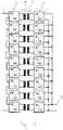
- Fig. 2shows a transformer assembly according to an embodiment of the invention.
- the transformer assemblycomprises a first transformer stage 100 having a plurality of first-stage transformer cells 110 (in Fig. 2 : nine transformer cells 110).
- Each of the first-stage transformer cells 110comprises a converter 112 and a medium frequency transformer 114.
- the converter 112 and the medium frequency transformer 114are connected in series to each other, so that an input of the converter 112 forms the input of the cell 110, an output of the converter 112 is connected to an input winding of the MFT 114, and an output winding of the MFT forms the output of the cell 110.
- the inputs of the transformer cells 110are connected in a cascading manner to each other between the input lines forming the input 101 of the first transformer stage 100.
- the outputs of the transformer cells 110are connected in parallel to each other, and form the output 102 of the first transformer stage 100 (low-voltage AC output).
- the transformer assemblyfurther comprises a second transformer stage 200.
- the second transformer stage 200comprises a second-stage transformer cell 210.
- the second-stage transformer cell 210comprises a medium frequency transformer 214 and a converter 212 connected in series to each other.
- An input winding of the MFT 214forms the input of the cell 210
- an output winding of the MFT 214is connected to an input of the converter 212
- an output of the converter 212forms the output of the cell 210.
- the input of the cell 210forms the input 201 of the second transformer stage 200.
- the input 201 of the second transformer stage 200is connected to the output 102 of the first transformer stage 100.
- the output of the cell 210forms the output 202 of the second transformer stage 200, and thereby of the transformer assembly.
- the second-stage MFT 212is a high-power MFT, rated for the total rated power of the transformer assembly.
- the single second-stage cell 210can be replaced by a plurality of cells of corresponding lower ratings, arranged in parallel to each other.
- the input 101, 201 and output 102, 202refer to groups (pairs) of conductor lines forming the respective input / output shown in Fig. 1 .
- a connection between an input and an outputmeans a connection from any one of the conductors of the input to any one of the conductors of the output, and in particular from each of the conductors of the input to a respective one of the conductors of the output.
- the first-stage converters 112are shown as AC-AC converters connectable to an AC network. But, alternatively, they can be DC-AC converters connectable to a DC network.
- the second-stage converters 212are shown as AC-DC converters connectable to a low-power DC component (energy source, load and/or DC network). Alternatively, it can be an AC-AC converter connectable to an AC component.
- a lightning impulse breakdown voltage of the second-stage transformer cell 210is at least double of a lightning impulse breakdown voltage of one of the first-stage transformer cells 110.
- the lightning impulse breakdown voltageis the peak voltage of a lightning impulse between an input 101, 201 and an output 102, 202 of the respective transformer cell 110, 210, at which the respective transformer cell 110, 210 breaks down during a lightning impulse test according to IEC 60076-11:2004.
- the lightning impulse withstand voltage of the second-stage transformer cell 210may be at least double of a lightning impulse withstand voltage of one of the first-stage transformer cells 110.
- the lightning impulse withstand voltageis defined as the maximum voltage of a lightning impulse between an input 101, 201 and an output 102, 202 of the respective transformer cell 110, 210, which the respective transformer cell 110, 210 withstands during a lightning impulse test according to IEC 60076-11:2004.
- the MFT only of the second stage 200 but not of the first stage 100may require bushings.
- the first stage 100it may be sufficient to be able to operate at nominal voltage (e.g., 9 kV(peak) phase-to-ground in a medium voltage grid of 11 kV rms line-to-line) and to withstand partial discharge at this voltage level.
- nominal voltagee.g. 9 kV(peak) phase-to-ground in a medium voltage grid of 11 kV rms line-to-line
- partial dischargee.g. 9 kV(peak) phase-to-ground in a medium voltage grid of 11 kV rms line-to-line
- the first stage 100may be required to withstand a test voltage of 16.5 kV rms without partial discharge.
- the winding window of the first-stage MFTsis, therefore, well utilized.
- a big advantageis that no bushings may be provided for the first-stage cells 110, whereby considerable volume and weight savings are possible.
- Such bushingsmay be provided in the second-stage cells 210, in the example there is only a single second-stage cell 210 as opposed to 9 first-stage cells 110, so that there is a significant overall space and weight reduction.
- the number of second-stage cells 210(in parallel to each other) is at most half of the number of first-stage cells 110, and preferably at most 3 cells, at most 2 cells, or even only 1 cell.
- the first stage componentscan be realized by simple, reliable and low-cost air-insulated MFTs. Therefore, efficiency and cost can be kept relatively low.
- the first stage 100may be better optimized for high-voltage conversion by the converters of the plurality of the first-stage cells being connected to the first-stage input in a cascading manner; and for continuous operation at higher voltages compared to the second stage.
- the first-stage MFTsare advantageously unpotted. This allows the first-stage cells 110, which are subject to the highest insulation stresses, to be air-insulated. Thereby, cooling can be improved and the number of components that need to be considered for the long-term durability of the transformer assembly are reduced. This advantage is particularly pronounced in the case of the input 101 being connectable to a DC network, with associated DC insulation stresses.
- the MFTs of both stagescan be much better optimized than a state-of-the-art single-stage MFT. Especially for low power this results in improved overall performance. This is especially the case for low power ratings of up to 500 kW and especially of up to 200 MW rated power, and / or of grid voltages at the input side of up to 52 kV, especially up to 18 kV. For these ranges, in contrast to the comparative example of Fig. 1 , the size and volume savings due to insulation components related to the lightning impulse withstand requirements are particularly noticeable.
- the topology with two stageshas the potential to significantly simplify the design of the insulation system of the whole SST including the cooling system. Furthermore, due to the two stages capable of being optimized for different requirements, the system allows additional freedom in design of the SST, and allows improved cell and system optimization, e.g., by selection of optimized semiconductor components for each of the stages.
- respective inputs of the first-stage transformer cells 110are connected in a cascading manner between input terminals 101 of the Transformer assembly (which also constitutes an input of the first stage 100).
- windings of the medium frequency transformers 114 of the first-stage transformer cells 110are unpotted and/or air-insulated.
- the first transformer stage 100has a rated nominal withstand voltage of at least 5 kV, preferably of at least 10 kV.
- the first transformer stage 100has a rated nominal withstand voltage of not more than 52 kV.
- the first stagecomprises at least 2 first-stage cells 110, preferably at least six first-stage cells 110.
- the first-stage cellshave at least 10 kW and at most 100 kW, at most 50 kW, or only at most 30 kW power each.
- the second stagehas a single cell (or at most three cells) comprising a high-power MFT which is designed for fulfilling the LI test requirement.
- the transformer assemblyis configured for subjecting the second stage to voltages of no more than 5 kV, preferably of no more than 2 kV, at nominal operation (relative to ground). Thereby, even if potted or otherwise insulated, the second stage is not subjected to large voltage stresses and resulting partial discharge issues.
- the MFT(s) of the second stagehas is (are) insulated by a solid and/or liquid-insulation (e.g., oil-insulated).
- the solid insulationmay have a breakdown strength of at least 1 kV and/or a thickness of at least 1 mm.
- Such a solid insulationmay comprise a resin such as an epoxy resin, and/or may be obtained by potting or vacuum pressure impregnation.
- the second-stage MFT(s)has (have) terminals connected to the respective MFT through bushings (in particular, bushings designed to withstand a lightning impulse).
- the second transformer stage 200has a lightning impulse breakdown voltage and/or a rated lightning impulse withstand voltage of at least 50 kV, preferably of at least 80 kV.
- the at least one second-stage transformer cell 210is a single second-stage transformer cell 210, or alternatively a plurality of second-stage transformer cells 210 connected in parallel to each other. Thereby, several second-stage MFTs may be employed in parallel.
- the transformation ratio of the second transformer stage 200is between 1.0 and 10.0, and/or to not more than 3.0 or even not more than 2.0. According to an aspect, the transformation ratio of the second-stage MFT(s) is 1:1.
- the 1:1 ratiomay, for example, allow transformer windings by coaxial cables.
- the converter 212 of the second-stage transformer cell 210is one of an AC-to-DC converter or an AC-to-AC converter.
- the DC linkmay optionally provide an additional DC connection.
- the first- and second-stage transformer cellshave mutually different insulation properties.
- this differencehas been expressed in terms of the different lightning impulse breakdown voltage of the first- and second-stage transformer cells - namely, that the lightning impulse breakdown voltage of the second-stage transformer cell (e.g., of any one of the at least one second-stage transformer cell) is at least double of a lightning impulse breakdown voltage of one of the first-stage transformer cells.
- the lightning impulse breakdown voltageis the (minimum) peak voltage of a lightning impulse between an input and an output of the respective transformer cell, at which the respective transformer cell breaks down during a lightning impulse test.
- the different insulation propertiescan also be defined in a different manner, and some such definitions are given in the following aspects of the invention.
- the present disclosureshall encompass transformer cells with any combination of these differences, i.e., in which an alternative definition may be given instead of or in addition to the above definition in terms of the lightning impulse breakdown voltage, as long as the transformer assembly fulfils the conditions with respect to the lightning impulse breakdown voltage defined in claim 1.
- a lightning impulse withstand voltage of the second-stage transformer cellmay be at least double of a lightning impulse withstand voltage of one of the first-stage transformer cells.
- the lightning impulse withstand voltagedefines the voltage of a lightning impulse between an input and an output of the respective transformer cell, which the respective transformer cell is rated to withstand during a lightning impulse test.
- the transformer assemblycomprises two stages, each having MFTs with different insulations systems, so that the MFTs of the first stage are designed with a different insulation system than the MFT(s) of the second stage.
- the insulation of the first stageis designed for nominal medium voltage (e.g. 10 kV .. 50 kV) but not for LI pulse protection
- the insulation strength of the second stageis designed for nominal low voltage (e.g. 0.2 kV .. 2kV) and for LI pulse protection, the LI pulse having a voltage of at least three times of the nominal voltage.
- the winding of the medium frequency transformer 214 of the second-stage transformer cell 210is encapsulated by an additional (and/or thicker) solid- or liquid-insulator encapsulation, compared to corresponding windings of the medium frequency transformers 114 of the first-stage transformer cells 110.
- a corresponding solid- or liquid-insulator encapsulationmay be absent (or thinner) from the windings of the first-stage medium frequency transformers 114.
- the medium frequency transformer 214 of the second-stage transformer cell 210has an additional (or larger) bushing connecting a terminal to a winding of the medium frequency transformer 214, whereas the medium frequency transformers 114 of the first-stage transformer cells 110 lack a corresponding bushing, i.e., lacks a bushing of comparable dimensions, i.e., has no bushing or smaller bushing (e.g. half the size or smaller).
- the bushingmay be a solid encapsulation of the conductor portion leading to the winding of the respective medium frequency transformer (e.g., between the terminal and the medium frequency transformer's winding), having a high breakdown strength (above 1 kV) and typically a thickness of at least 1 mm.
- the bushingmay be integrated into the solid insulator encapsulation, or may be provided as a separate piece, possibly in direct contact with the insulator encapsulation.
- the size of the bushingcan be defined as the clearance distance between the respective exits of a pair of bushings.
- the clearance distance between any pair of bushing exits of the medium frequency transformer of the at least one second-stage transformer cell 210is larger than a clearance distance of a corresponding conductor pair of a medium frequency transformer of any one of the first-stage transformer cells 110.
- the at least one second-stage transformer cell 210has a larger clearance distance between a conductor connected to the winding and a grounded part than any one of the first-stage transformer cells 110.
- a winding of the medium frequency transformer 214 of the second-stage transformer cell 210has an additional solid or liquid insulation compared to the medium frequency transformer of any one of the first-stage transformer cells 110.
- the insulation of the second-stage medium frequency transformer 214may be, e.g., thicker and/or have a higher breakdown voltage than the first-stage medium frequency transformer 114.
- the medium frequency transformer 214 of the second-stage transformer cell 210may be liquid-insulated and/or solid-insulated (e.g., by potting or vacuum pressure impregnation), whereas the windings of the medium frequency transformers (114) of the first-stage transformer cells (110) may lack a corresponding insulation (of comparable thickness and/or breakdown strength, e.g., no insulation by a thickness of 1 mm or more), e.g., may be non-liquid-insulated, non-potted, and non-insulated by vacuum pressure impregnation.
- the transformation ratio of the first transformer stage 100is more than the transformation ratio of the second transformer stage 200.
- the transformation ratiois defined as the input voltage divided by the transformed output voltage of the respective transformer stage.
- any one of the medium frequency transformers 114 of the first-stage transformer cells 110has at most half the mass and/or half the volume of the medium frequency transformer 214 of any one of the at least one second-stage transformer cell 210.
- the number of cells 110 of the first transformer stage 100is more than the number of cells 210 of the second transformer stage 200, preferably by at least a factor 1,5, by a factor 2,0, or even by a factor 3,0.
- the number of first-stage transformer cells 110 of the first transformer stage 100is larger than the number of the at least one second-stage transformer cell 210 of the second transformer stage 200, preferably by a factor of at least 2, and particularly preferably by a factor of at least 4.
- the transformation ratio of the second transformer stage 200is smaller than that of the first transformer stage 100, by at least 50% of the transformation ratio of the first transformer stage 100.
- the first and second stages 100, 200are connected in series to each other between input and output terminals 101, 202 of the Transformer assembly, so that an input of the second stage 200 is an output of the first stage 100.
- respective outputs of the first-stage transformer cells 110are connected, in parallel to each other, to the output 102 of the first stage 100 and thereby to the input 201 of the second stage.
- the transformer assemblyis configured for the input terminal at the input 101 of the first transformer stage being connected to a higher nominal voltage, and for an output terminal at the output 202 of the second transformer stage being connected to a lower nominal voltage.
- the transformer assemblyis comprised in a Solid State Transformer (SST).
- SSTSolid State Transformer
- a surge arresteris connected to the input of the transformer assembly.
- the surge arresteris configured for limiting the voltage stress on the first-stage MFTs to a value below their dielectric strength.
- the Solid State Transformercomprises a plurality of transformer assemblies as described herein, e.g., one or more for each phase.
- the transformer assemblyis adapted for an input voltage of up to 52 kV, preferably of up to 18 kV (e.g., a medium voltage grid), and/or of at least 1 kV, preferably at least 5 kV, being connected to the input of the transformer assembly.
- the transformer assemblyis adapted for an output voltage of no more than 1 kV, and/or of at least 110 V, preferably at least 230 V, in particular at least 300 V (e.g., a low voltage grid) being connected to the input of the transformer assembly.
- the transformer assemblyis adapted for a power of at least 100 kW, and/or at most 100 MW, preferably at most 1 MW.
- the SSTis used for connecting a renewable energy source such as solar or wind, a battery, and/or an electric vehicle on its output to a grid at its input.
- a renewable energy sourcesuch as solar or wind
- a batteryand/or an electric vehicle on its output
- the term "input”is used for a higher-voltage side
- the term “output”is used for a lower-voltage side, but does not imply a direction of power flow.
- the SSTmay be configured for transmitting power from the input to the output, or from the output to the input, or both.
Landscapes
- Engineering & Computer Science (AREA)
- Power Engineering (AREA)
- Physics & Mathematics (AREA)
- General Physics & Mathematics (AREA)
- Emergency Protection Circuit Devices (AREA)
- Ac-Ac Conversion (AREA)
- Coils Of Transformers For General Uses (AREA)
- Testing Relating To Insulation (AREA)
Description
- Aspects of the invention relate to a transformer assembly with medium frequency transformers (MFTs), in particular having transformer cells each comprising a converter and an MFT. Further aspects relate to a Solid State Transformer having such a transformer assembly.
- There is high interest in medium frequency transformers (MFT) due to their potential to save weight and space. Herein, an MFT is defined as operating in a frequency range of 100 Hz to 100 kHz. This increased frequency allows shrinking of the magnetic components (the MFTs) due to the increased switching frequency, compared to conventional transformers operating at network frequencies of 50-60 Hz. Therefore, Solid State Transformers using MFTs have the potential to save space and weight, and in some cases cost, compared to conventional transformers even if additional frequency converters are needed.
Figure 1 shows, as a comparative example, an exemplary transformer assembly for one phase of a solid state transformer (SST). The transformer assembly has an input 11 connected to a medium voltage grid of typically 11 kV (rms, line-to-line). The transformer assembly has a plurality of (here: 9)transformer cells 10 whose inputs (i.e. the inputs of their input converters 12) are connected to the medium voltage grid in a cascading manner. Each of thetransformer cells 10 has aninput converter 12, anMFT 14, and anoutput converter 16. In eachcell 10, the output of theinput converter 12 is connected to the input winding ofMFT 14 at the MFT's frequency; and likewise the input of theoutput converter 16 is connected to the output winding ofMFT 14 at the MFT's frequency. The outputs of the transformer cells 10 (i.e. the outputs of their output converters 16) are connected in a parallel to theoutput 18 of the transformer assembly.- In a solid state transformer (SST) the
individual cells 10 typically need to meet defined insulation requirements with respect to the medium voltage network. For example, the insulation requirements include the ability to operate under nominal voltages without partial discharge; but also to withstand a higher withstand voltages, and in particular to withstand short high-voltage bursts of e.g. a lightning impulse. - For example, in a medium voltage network of 11 kV and with 9 cells, the nominal voltage for each cell is about 1 kV (the network voltage 11kV rms line-to-line relates to a peak voltage of 9 kV in a Dy-configuration, which is divided by the number of cells). In addition, the cascaded cells must withstand higher voltages (for example, 2.5 times nominal voltage stress) without partial discharge.
- Herein, unless stated otherwise, all AC voltages are understood to be rms voltages. Also, voltages refer to actual voltages including contributions from applied and induced voltages of windings. Here, the applied voltage is referred to as a voltage between a primary and a secondary winding, where the primary winding is entirely on one potential, and the secondary is entirely on another potential. For the first stage, because of the series connection of the cells on the grid side (input side), the applied voltage dominates.
- The ability to withstand short high-voltage bursts of a lightning impulse is tested by a lightning impulse test. Herein the lightning impulse test is understood to be the standard lightning impulse test as defined in the pertinant standards, e.g. in IEC 60076-11:2004. According to this test, each
cell 10 must withstand a short high-voltage burst of 95 kV (peak) between the input 11 and theoutput 18 of the transformer assembly and thus in the worst case between the input and the output of each of thetransformer cells 10. - The above example shows that the LI (lightning impulse) of 95 kV (peak) is considerably higher than any of the other voltages the transformer assembly needs to be able to withstand. Especially due to these requirements for the high-voltage lightning impulse (LI) test, much higher than the nominal voltage, the insulation distances have to be very large. These insulation distances result in each of the MFT cells being rather large and voluminous.
- In order to fulfil the LI test conditions, furthermore, potting of the winding (e.g., an insulating epoxy encapsulation of the windings) is employed. This may result in further engineering challenges for cooling and regarding partial discharges. Additionally, large bushings are required for each MFT which further add to the cost and volume of the transformer.
- Since the MFTs are required to fulfil the above insulation requirements irrespective of power, especially for small power the insulation due to the LI withstand requirements dominates the volume of each MFT. Therefore, in this domain one of the key advantages of MFT-based systems, i.e., their potential for small size and low weight, is critically reduced.
- Thus, there is a need for an MFT-based transformer assembly in which the above disadvantages are at least reduced.
- Swiss patent application publication no.
CH 706 332 A2 - Chinese utility model application publication
CN 204928163 U describes an outer power supply system of a high voltage Static VAR Generator (SVG) power unit. The power supply system has a two-stage isolation transformer resistant to high voltage differentials. A high voltage resistant power frequency isolation transformer having a glass encapsulation of vacuum epoxy is adopted in the second level high voltage isolation transformer to solve the problems caused by a voltage differential to the SVG power unit. - In view of the above, the present invention provides a transformer assembly and a solid state transformer according to the claims that follow.
- According to a first aspect, the transformer assembly comprises a first transformer stage having a plurality of first-stage transformer cells, each of the first-stage transformer cells comprising a converter and a medium frequency transformer connected in series to each other, wherein the respective inputs of each of the plurality of first-stage transformer cells are connected in series and the respective outputs of each of the plurality first-stage transformer cells are connected in parallel to form the output of the first transformer stage; and a second transformer stage comprising at least one second-stage transformer cell, the second-stage transformer cell comprising a medium frequency transformer and a converter connected in series to each other. A lightning impulse breakdown voltage of the at least one second-stage transformer cell is at least double of a lightning impulse breakdown voltage of one of the first-stage transformer cells. The lightning impulse breakdown voltage is the peak voltage of a lightning impulse between an input and an output of the respective transformer cell, at which the respective transformer cell breaks down during a lightning impulse test. An input of the second transformer stage is connected to the output of the first transformer stage.
- According to a second aspect, there is provided a Solid State Transformer having the transformer assembly according to the first aspect.
- A potential advantage of this two-stage topology of the transformer assembly is that the insulation distances, especially in the first stage, can be significantly reduced, especially if no bushings and/or no potting is provided for the first-stage cells. As a result, considerable volume and weight savings are possible. Furthermore, the MFTs of both stages may be advantageously optimized for different requirements. These advantages are especially relevant for low power, e.g., up to 500 MW rated power.
- The transformer assembly of the first aspect may also be used in a method for operating the transformer assembly and/or a solid state transformer comprising the same. The method comprises inputting an input DC or AC current to the first transformer stage, converting the inputted current to a medium frequency current (i.e. generating the medium frequency current as an output by using the input current's energy) using the converters of the first-stage transformer cells, and transforming the converted medium frequency current using the first-stage medium frequency transformers of the first-stage transformer cells; and transforming the transformed current (transformed by the first-stage transformer cell) to the second-stage transformer cell. The method may further include transforming the fed current using the at least one second-stage medium frequency transformer of the at least one second-stage transformer cell; and converting the resulting current using the converter of the at least one second-stage transformer cell.
- Further advantages, features, aspects and details that can be combined with embodiments described herein are evident from the dependent claims, the description and the drawings.
- The details will be described in the following with reference to the figures, wherein
- Fig. 1
- is a schematic view of a transformer assembly being a comparative example; and
- Fig. 2
- is a schematic view of a transformer assembly according to an embodiment of the invention.
- Reference will now be made in detail to various embodiments and aspects of the invention, some of which are illustrated in
Fig. 2 . Each example is provided by way of explanation and is not meant as a limitation. For example, features illustrated or described as part of one aspect or embodiment can be used on or in conjunction with any other aspect or embodiment. It is intended that the present disclosure includes such combinations, modifications and variations. Fig. 2 shows a transformer assembly according to an embodiment of the invention. The transformer assembly comprises afirst transformer stage 100 having a plurality of first-stage transformer cells 110 (inFig. 2 : nine transformer cells 110). Each of the first-stage transformer cells 110 comprises a converter
112 and amedium frequency transformer 114. Theconverter 112 and themedium frequency transformer 114 are connected in series to each other, so that an input of theconverter 112 forms the input of thecell 110, an output of theconverter 112 is connected to an input winding of theMFT 114, and an output winding of the MFT forms the output of thecell 110.- The inputs of the
transformer cells 110 are connected in a cascading manner to each other between the input lines forming theinput 101 of thefirst transformer stage 100. The outputs of thetransformer cells 110 are connected in parallel to each other, and form theoutput 102 of the first transformer stage 100 (low-voltage AC output). - The transformer assembly further comprises a
second transformer stage 200. Thesecond transformer stage 200 comprises a second-stage transformer cell 210. The second-stage transformer cell 210 comprises amedium frequency transformer 214 and aconverter 212 connected in series to each other. An input winding of theMFT 214 forms the input of thecell 210, an output winding of theMFT 214 is connected to an input of theconverter 212, and an output of theconverter 212 forms the output of thecell 210. - The input of the
cell 210 forms theinput 201 of thesecond transformer stage 200. Theinput 201 of thesecond transformer stage 200 is connected to theoutput 102 of thefirst transformer stage 100. The output of thecell 210 forms the output 202 of thesecond transformer stage 200, and thereby of the transformer assembly. In the example ofFig. 2 , the second-stage MFT 212 is a high-power MFT, rated for the total rated power of the transformer assembly. Alternatively, the single second-stage cell 210 can be replaced by a plurality of cells of corresponding lower ratings, arranged in parallel to each other. - Here, the
input output 102, 202 refer to groups (pairs) of conductor lines forming the respective input / output shown inFig. 1 . A connection between an input and an output means a connection from any one of the conductors of the input to any one of the conductors of the output, and in particular from each of the conductors of the input to a respective one of the conductors of the output. - The first-
stage converters 112 are shown as AC-AC converters connectable to an AC network. But, alternatively, they can be DC-AC converters connectable to a DC network. Likewise, the second-stage converters 212 are shown as AC-DC converters connectable to a low-power DC component (energy source, load and/or DC network). Alternatively, it can be an AC-AC converter connectable to an AC component. - With the two-stage topology of the transformer assembly as shown in
Fig. 2 , it is sufficient that only thesecond stage 200 but not necessarily thefirst stage 100 meets the lightning impulse withstand requirements. The additional insulation requirements related to the lightning test, as described above with respect to the comparative example ofFig. 1 , therefore only apply for thesecond stage 200 but not necessarily to thefirst stage 100. This high-power MFT ("second-stage") provides the insulation for 50 Hz-withstand test and lightning impulse (LI) test. The multiple first-stage-MFTs which are directly connected to the cells, provide insulation for the nominal operation, but don't have to be designed for the LI test. - More precisely, according to the invention, a lightning impulse breakdown voltage of the second-
stage transformer cell 210 is at least double of a lightning impulse breakdown voltage of one of the first-stage transformer cells 110. Herein, the lightning impulse breakdown voltage is the peak voltage of a lightning impulse between aninput output 102, 202 of therespective transformer cell respective transformer cell - From another point of view, the lightning impulse withstand voltage of the second-
stage transformer cell 210 may be at least double of a lightning impulse withstand voltage of one of the first-stage transformer cells 110. Herein, the lightning impulse withstand voltage is defined as the maximum voltage of a lightning impulse between aninput output 102, 202 of therespective transformer cell respective transformer cell - Thereby, due to the lower discharge requirements for the
first stage 100, it is possible to use compact and lightweight components for thefirst stage 100. For example, the MFT only of thesecond stage 200 but not of thefirst stage 100 may require bushings. - For the
first stage 100, it may be sufficient to be able to operate at nominal voltage (e.g., 9 kV(peak) phase-to-ground in a medium voltage grid of 11 kV rms line-to-line) and to withstand partial discharge at this voltage level. For example, for a network voltage (nominal rms voltage line-to-line) of 11 kV, thefirst stage 100 may be required to withstand a test voltage of 16.5 kV rms without partial discharge. - This requirement of the
first stage 100 allows relatively small insulation distances. The winding window of the first-stage MFTs is, therefore, well utilized. A big advantage is that no bushings may be provided for the first-stage cells 110, whereby considerable volume and weight savings are possible. Although such bushings may be provided in the second-stage cells 210, in the example there is only a single second-stage cell 210 as opposed to 9 first-stage cells 110, so that there is a significant overall space and weight reduction. More generally, the number of second-stage cells 210 (in parallel to each other) is at most half of the number of first-stage cells 110, and preferably at most 3 cells, at most 2 cells, or even only 1 cell. - Furthermore, also regarding some further insulation requirements, e.g., for air insulation distances according to standards, it is sufficient if such insulation requirements are fulfilled by the
second stage 200, but not necessarily by thefirst stage 100. - Thereby, the first stage components can be realized by simple, reliable and low-cost air-insulated MFTs. Therefore, efficiency and cost can be kept relatively low.
- On the other hand, the
first stage 100 may be better optimized for high-voltage conversion by the converters of the plurality of the first-stage cells being connected to the first-stage input in a cascading manner; and for continuous operation at higher voltages compared to the second stage. - For this purpose, the first-stage MFTs are advantageously unpotted. This allows the first-
stage cells 110, which are subject to the highest insulation stresses, to be air-insulated. Thereby, cooling can be improved and the number of components that need to be considered for the long-term durability of the transformer assembly are reduced. This advantage is particularly pronounced in the case of theinput 101 being connectable to a DC network, with associated DC insulation stresses. - Thus, overall, the MFTs of both stages can be much better optimized than a state-of-the-art single-stage MFT. Especially for low power this results in improved overall performance. This is especially the case for low power ratings of up to 500 kW and especially of up to 200 MW rated power, and / or of grid voltages at the input side of up to 52 kV, especially up to 18 kV. For these ranges, in contrast to the comparative example of
Fig. 1 , the size and volume savings due to insulation components related to the lightning impulse withstand requirements are particularly noticeable. - As a further advantage, the topology with two stages has the potential to significantly simplify the design of the insulation system of the whole SST including the cooling system. Furthermore, due to the two stages capable of
being optimized for different requirements, the system allows additional freedom in design of the SST, and allows improved cell and system optimization, e.g., by selection of optimized semiconductor components for each of the stages. - While the foregoing is directed to embodiments, other and further embodiments may be devised as long as they are within the scope of the claims.
- First, aspects relating to the first stage are described.
- According to the invention, respective inputs of the first-
stage transformer cells 110 are connected in a cascading manner betweeninput terminals 101 of the Transformer assembly (which also constitutes an input of the first stage 100). According to an aspect, windings of themedium frequency transformers 114 of the first-stage transformer cells 110 are unpotted and/or air-insulated. According to an aspect, thefirst transformer stage 100 has a rated nominal withstand voltage of at least 5 kV, preferably of at least 10 kV. According to an aspect, thefirst transformer stage 100 has a rated nominal withstand voltage of not more than 52 kV. - According to an aspect, the first stage comprises at least 2 first-
stage cells 110, preferably at least six first-stage cells 110. According to an aspect, the first-stage cells have at least 10 kW and at most 100 kW, at most 50 kW, or only at most 30 kW power each. - Next, aspects relating to the second stage are described.
- According to an aspect, the second stage has a single cell (or at most three cells) comprising a high-power MFT which is designed for fulfilling the LI test requirement. According to an aspect the transformer assembly is configured for subjecting the second stage to voltages of no more than 5 kV, preferably of no more than 2 kV, at nominal operation (relative to ground). Thereby, even if potted or otherwise insulated, the second stage is not subjected to large voltage stresses and resulting partial discharge issues.
- According to an aspect, the MFT(s) of the second stage has is (are) insulated by a solid and/or liquid-insulation (e.g., oil-insulated). The solid insulation may have a breakdown strength of at least 1 kV and/or a thickness of at least 1 mm. Such a solid insulation may comprise a resin such as an epoxy resin, and/or may be obtained by potting or vacuum pressure impregnation. According to an aspect, the second-stage MFT(s) has (have) terminals connected to the respective MFT through bushings (in particular, bushings designed to withstand a lightning impulse).
- According to an aspect, the
second transformer stage 200 has a lightning impulse breakdown voltage and/or a rated lightning impulse withstand voltage of at least 50 kV, preferably of at least 80 kV. - According to an aspect, the at least one second-
stage transformer cell 210 is a single second-stage transformer cell 210, or alternatively a plurality of second-stage transformer cells 210 connected in parallel to each other. Thereby, several second-stage MFTs may be employed in parallel. - According to an aspect, the transformation ratio of the
second transformer stage 200 is between 1.0 and 10.0, and/or to not more than 3.0 or even not more than 2.0. According to an aspect, the transformation ratio of the second-stage MFT(s) is 1:1. The 1:1 ratio may, for example, allow transformer windings by coaxial cables. - According to an aspect, the
converter 212 of the second-stage transformer cell 210 is one of an AC-to-DC converter or an AC-to-AC converter. In case of an AC-to-AC converter, the DC link may optionally provide an additional DC connection. - Next, aspects relating to the comparison of the first and second stages are described.
- According to an aspect, the first- and second-stage transformer cells have mutually different insulation properties. In the Summary of Invention (and in claim 1), this difference has been expressed in terms of the different lightning impulse breakdown voltage of the first- and second-stage transformer cells - namely, that the lightning impulse breakdown voltage of the second-stage transformer cell (e.g., of any one of the at least one second-stage transformer cell) is at least double of a lightning impulse breakdown voltage of one of the first-stage transformer cells. Herein, the lightning impulse breakdown voltage is the (minimum) peak voltage of a lightning impulse between an input and an output of the respective transformer cell, at which the respective transformer cell breaks down during a lightning impulse test.
- The different insulation properties can also be defined in a different manner, and some such definitions are given in the following aspects
of the invention. The present disclosure shall encompass transformer cells with any combination of these differences, i.e., in which an alternative definition may be given instead of or in addition to the above definition in terms of the lightning impulse breakdown voltage, as long as the transformer assembly fulfils the conditions with respect to the lightning impulse breakdown voltage defined in claim 1. - For example, according to a further aspect, a lightning impulse withstand voltage of the second-stage transformer cell may be at least double of a lightning impulse withstand voltage of one of the first-stage transformer cells. Herein, the lightning impulse withstand voltage defines the voltage of a lightning impulse between an input and an output of the respective transformer cell, which the respective transformer cell is rated to withstand during a lightning impulse test.
- According to a further aspect, the transformer assembly comprises two stages, each having MFTs with different insulations systems, so that the MFTs of the first stage are designed with a different insulation system than the MFT(s) of the second stage. In particular, the insulation of the first stage is designed for nominal medium voltage (e.g. 10 kV .. 50 kV) but not for LI pulse protection, and the insulation strength of the second stage is designed for nominal low voltage (e.g. 0.2 kV .. 2kV) and for LI pulse protection, the LI pulse having a voltage of at least three times of the nominal voltage.
- According to an aspect, the winding of the
medium frequency transformer 214 of the second-stage transformer cell 210 is encapsulated by an additional (and/or thicker) solid- or liquid-insulator encapsulation, compared to corresponding windings of themedium frequency transformers 114 of the first-stage transformer cells 110. A corresponding solid- or liquid-insulator encapsulation may be absent (or thinner) from the windings of the first-stagemedium frequency transformers 114. - According to an aspect, the
medium frequency transformer 214 of the second-stage transformer cell 210 has an additional (or larger) bushing connecting a terminal to a winding of themedium frequency transformer 214, whereas themedium frequency transformers 114 of the first-stage transformer cells 110 lack a corresponding bushing, i.e., lacks a bushing of comparable dimensions, i.e., has no bushing or smaller bushing (e.g. half the size or smaller). The bushing may be a solid encapsulation of the conductor portion leading to the winding of the respective medium frequency transformer (e.g., between the terminal and the medium frequency transformer's winding), having a high breakdown strength (above 1 kV) and typically a thickness of at least 1 mm. The bushing may be integrated into the solid insulator encapsulation, or may be provided as a
separate piece, possibly in direct contact with the insulator encapsulation. In such a case, the size of the bushing can be defined as the clearance distance between the respective exits of a pair of bushings. Thus, according to an aspect, the clearance distance between any pair of bushing exits of the medium frequency transformer of the at least one second-stage transformer cell 210 is larger than a clearance distance of a corresponding conductor pair of a medium frequency transformer of any one of the first-stage transformer cells 110. - According to a further aspect, the at least one second-
stage transformer cell 210 has a larger clearance distance between a conductor connected to the winding and a grounded part than any one of the first-stage transformer cells 110. - According to a further aspect, a winding of the
medium frequency transformer 214 of the second-stage transformer cell 210 has an additional solid or liquid insulation compared to the medium frequency transformer of any one of the first-stage transformer cells 110. Thereby, the insulation of the second-stagemedium frequency transformer 214 may be, e.g., thicker and/or have a higher breakdown voltage than the first-stagemedium frequency transformer 114. For example, themedium frequency transformer 214 of the second-stage transformer cell 210 may be liquid-insulated and/or solid-insulated (e.g., by potting or vacuum pressure impregnation), whereas the windings of the medium frequency transformers (114) of the first-stage transformer cells (110) may lack a corresponding insulation (of comparable thickness and/or breakdown strength, e.g., no insulation by a thickness of 1 mm or more), e.g., may be non-liquid-insulated, non-potted, and non-insulated by vacuum pressure impregnation. - According to an aspect, the transformation ratio of the
first transformer stage 100 is more than the transformation ratio of thesecond transformer stage 200. Herein, the transformation ratio is defined as the input voltage divided by the transformed output voltage of the respective transformer stage. - According to an aspect, any one of the
medium frequency transformers 114 of the first-stage transformer cells 110 has at most half the mass and/or half the volume of themedium frequency transformer 214 of any one of the at least one second-stage transformer cell 210. - According to an aspect, the number of
cells 110 of thefirst transformer stage 100 is more than the number ofcells 210 of thesecond transformer stage 200, preferably by at least a factor 1,5, by afactor 2,0, or even by a factor 3,0. - According to an aspect, the number of first-
stage transformer cells 110 of thefirst transformer stage 100 is larger than the number of the at least one second-stage transformer cell 210 of thesecond transformer stage 200, preferably by a factor of at least 2, and particularly preferably by a factor of at least 4. - According to an aspect, the transformation ratio of the
second transformer stage 200 is smaller than that of thefirst transformer stage 100, by at least 50% of the transformation ratio of thefirst transformer stage 100. - Next, aspects relating to interconnections within the transformer assembly are described. According to the invention, the first and
second stages output terminals 101, 202 of the Transformer assembly, so that an input of thesecond stage 200 is an output of thefirst stage 100. - According to the invention, respective outputs of the first-
stage transformer cells 110 are connected, in parallel to each other, to theoutput 102 of thefirst stage 100 and thereby to theinput 201 of the second stage. - According to an aspect, the transformer assembly is configured for the input terminal at the
input 101 of the first transformer stage being connected to a higher nominal voltage, and for an output terminal at the output 202 of the second transformer stage being connected to a lower nominal voltage. - Next, further aspects relating to the transformer assembly and its parameters are described.
- According to an aspect, the transformer assembly is comprised in a Solid State Transformer (SST). According to an aspect, a surge arrester is connected to the input of the transformer assembly. According to an aspect, the surge arrester is configured for limiting the voltage stress on the first-stage MFTs to a value below their dielectric strength.
- According to an aspect, the Solid State Transformer comprises a plurality of transformer assemblies as described herein, e.g., one or more for each phase.
- According to an aspect, the transformer assembly is adapted for an input voltage of up to 52 kV, preferably of up to 18 kV (e.g., a medium voltage grid), and/or of at least 1 kV, preferably at least 5 kV, being connected to the input of the transformer assembly. According to an aspect, the transformer assembly is adapted for an output voltage of no more than 1 kV, and/or of at least 110 V, preferably at least 230 V, in particular at least 300 V (e.g., a low voltage grid) being connected to the input of the transformer assembly.
- According to an aspect, the transformer assembly is adapted for a power of at least 100 kW, and/or at most 100 MW, preferably at most 1 MW.
- According to an aspect, the SST is used for connecting a renewable energy source such as solar or wind, a battery, and/or an electric vehicle on its output to a grid at its input. Herein, the term "input" is used for a higher-voltage side, and the term "output" is used for a lower-voltage side, but does not imply a direction of power flow. The SST may be configured for transmitting power from the input to the output, or from the output to the input, or both.
Claims (14)
- Transformer assembly (1) comprising:- a first transformer stage (100) having a plurality of first-stage transformer cells (110), each of the first-stage transformer cells (110) comprising a converter (112) and a medium frequency transformer (114) connected in series to each other, wherein respective inputs of each of the plurality of first-stage transformer cells (110) are connected in series and respective outputs of each of the plurality first-stage transformer cells (110) are connected in parallel to form an output (102) of the first transformer stage (100); and- a second transformer stage (200) comprising at least one second-stage transformer cell (210), the second-stage transformer cell (210) comprising a medium frequency transformer (214) and a converter (212) connected in series to each other, whereina lightning impulse breakdown voltage of the at least one second-stage transformer cell (210) is at least double of a lightning impulse breakdown voltage of one of the first-stage transformer cells (110), wherein the lightning impulse breakdown voltage is the peak voltage of a lightning impulse between an input and an output of the respective transformer cell (110, 210), at which the respective transformer cell (110, 210) breaks down during a lightning impulse test, and whereinan input (201) of the second transformer stage (200) is connected to the output (102) of the first transformer stage (100).
- Transformer assembly (1) according to claim 1, wherein the at least one second-stage transformer cell (210) is a plurality of second-stage transformer cells (210) connected in parallel to each other.
- Transformer assembly (1) according to any of the preceding claims, wherein a transformation ratio of the first transformer stage (100) is more than a transformation ratio of the second transformer stage (200).
- Transformer assembly (1) according to any of the preceding claims, wherein a transformation ratio of the second transformer stage (200) is between 1.0 and 10.0.
- Transformer assembly (1) according to any of the preceding claims, wherein a winding of the medium frequency transformer (214) of the at least one second-stage transformer cell (210) has an additional solid or liquid insulation compared to the plurality of first-stage transformer cells (110).
- Transformer assembly (1) according to any of the preceding claims, wherein the number of first-stage transformer cells (110) of the first transformer stage (100) is larger than the number of the at least one second-stage transformer cell (210) of the second transformer stage (200), preferably by a factor of at least 2, and particularly preferably by a factor of at least 4.
- Transformer assembly (1) according to any of the preceding claims, wherein the medium frequency transformer (214) of the at least one second-stage transformer cell (210) comprises at least one bushing designed for withstanding a lightning impulse.
- Transformer assembly (1) according to any of the preceding claims, wherein the medium frequency transformer (114) of any one of the plurality of first-stage transformer cells (110) has at most half the mass of the medium frequency transformer (214) of any one of the at least one second-stage transformer cell (210).
- Transformer assembly (1) according to any of the preceding claims, wherein respective outputs of the plurality of first-stage transformer cells (110) are connected to the output (102) of the first transformer stage (100) and thereby to the input (201) of the second transformer stage (200).
- Transformer assembly (1) according to any of the preceding claims, having a higher-voltage input terminal at an input (101) of the first transformer stage (100), and a lower-voltage output terminal at an output (202) of the second transformer stage (200).
- Transformer assembly (1) according to any of the preceding claims, wherein the converter (212) of the at least one second-stage transformer cell (210) is one of an AC-to-DC converter or an AC-to-AC converter.
- Transformer assembly (1) according to any of the preceding claims, wherein an input of the transformer assembly (1) is connected to a surge arrester.
- Transformer assembly (1) according to any of the preceding claims, wherein the input of each of the medium frequency transformers (114) of the plurality of first-stage transformer cells (110) is connected to a surge arrester.
- Solid State Transformer having the transformer assembly (1) according to any of the preceding claims.
Priority Applications (3)
| Application Number | Priority Date | Filing Date | Title |
|---|---|---|---|
| EP19186462.8AEP3767653B1 (en) | 2019-07-16 | 2019-07-16 | Transformer assembly with medium frequency transformers |
| US16/925,999US11480602B2 (en) | 2019-07-16 | 2020-07-10 | Transformer assembly with medium frequency transformers |
| CN202010673128.XACN112242791B (en) | 2019-07-16 | 2020-07-14 | Transformer assembly with intermediate frequency transformer |
Applications Claiming Priority (1)
| Application Number | Priority Date | Filing Date | Title |
|---|---|---|---|
| EP19186462.8AEP3767653B1 (en) | 2019-07-16 | 2019-07-16 | Transformer assembly with medium frequency transformers |
Publications (2)
| Publication Number | Publication Date |
|---|---|
| EP3767653A1 EP3767653A1 (en) | 2021-01-20 |
| EP3767653B1true EP3767653B1 (en) | 2023-01-11 |
Family
ID=67314629
Family Applications (1)
| Application Number | Title | Priority Date | Filing Date |
|---|---|---|---|
| EP19186462.8AActiveEP3767653B1 (en) | 2019-07-16 | 2019-07-16 | Transformer assembly with medium frequency transformers |
Country Status (3)
| Country | Link |
|---|---|
| US (1) | US11480602B2 (en) |
| EP (1) | EP3767653B1 (en) |
| CN (1) | CN112242791B (en) |
Families Citing this family (4)
| Publication number | Priority date | Publication date | Assignee | Title |
|---|---|---|---|---|
| EP3767653B1 (en)* | 2019-07-16 | 2023-01-11 | ABB Schweiz AG | Transformer assembly with medium frequency transformers |
| CN113985191B (en)* | 2021-12-29 | 2022-04-19 | 苏州电器科学研究院股份有限公司 | System and method for testing short circuit bearing capacity of extra-high voltage transformer |
| CN114665716B (en)* | 2022-04-13 | 2024-12-27 | 国网智能电网研究院有限公司 | A high voltage DC transformer and system |
| CN115458276A (en)* | 2022-10-13 | 2022-12-09 | Abb瑞士股份有限公司 | Winding, transformer and switching power supply |
Family Cites Families (38)
| Publication number | Priority date | Publication date | Assignee | Title |
|---|---|---|---|---|
| US3820006A (en)* | 1972-11-24 | 1974-06-25 | Programmed Power | Power converter apparatus and silicon controlled rectifier switching circuit therefor |
| US4763237A (en)* | 1986-10-17 | 1988-08-09 | Wieczorek John P | DC/AC/DC Power conversion system including parallel transformers |
| SU1617566A1 (en)* | 1987-11-17 | 1990-12-30 | Винницкий Завод Радиотехнической Аппаратуры | Single-end d.c. voltage converter |
| DE4034100A1 (en)* | 1990-10-26 | 1992-04-30 | Armin Pengel | Lightning energy storage plant with voltage distribution transformers - arranged in simple, parallel and series circuits with sec. winding output rectifiers and storage capacitors |
| US5943229A (en)* | 1998-06-02 | 1999-08-24 | Abb Power T&D Company Inc. | Solid state transformer |
| CN1427428A (en)* | 2001-12-20 | 2003-07-02 | 王巨丰 | High efficiency lightning protection transformer |
| US7212419B2 (en)* | 2004-02-24 | 2007-05-01 | Vlt, Inc. | Adaptively configured and autoranging voltage transformation module arrays |
| US7304872B1 (en)* | 2004-09-24 | 2007-12-04 | Field Metrics, Inc. | Power supply |
| US9407093B2 (en)* | 2007-08-22 | 2016-08-02 | Maxout Renewables, Inc. | Method for balancing circuit voltage |
| CN101414791B (en)* | 2008-12-02 | 2014-03-26 | 福州大学 | Differential decompression DC chopper type high-frequency chain inverter |
| CN101534054B (en)* | 2009-04-14 | 2012-04-18 | 福州大学 | Single-isolation combination pressure increase and reduction type multi-input direct current converter |
| CN101630837A (en)* | 2009-06-30 | 2010-01-20 | 中山市澳美电子科技有限公司 | Ground-free lightning arrester |
| CH706337B1 (en)* | 2012-04-02 | 2016-04-15 | Eth Zürich Eth Transfer | Converter circuit and method for driving a converter circuit. |
| CN102638114B (en)* | 2012-04-24 | 2014-09-03 | 深圳市深泰明科技有限公司 | Power supply device of current transformer |
| ES2705048T3 (en)* | 2012-08-10 | 2019-03-21 | Sts Spezial Transf Stockach Gmbh & Co Kg | Medium frequency transformer |
| EP2824822B1 (en)* | 2013-07-09 | 2017-05-03 | ABB Schweiz AG | A power transmission and distribution system supplying a plurality of subsea loads |
| DE102014201955A1 (en)* | 2014-02-04 | 2015-08-06 | Siemens Aktiengesellschaft | On-board unit for a rail vehicle |
| US9374016B2 (en)* | 2014-06-24 | 2016-06-21 | Fuji Electric Co., Ltd. | AC-DC converter |
| US9520798B2 (en)* | 2014-08-26 | 2016-12-13 | General Electric Company | Multi-level DC-DC converter with galvanic isolation and adaptive conversion ratio |
| CN204119215U (en)* | 2014-10-12 | 2015-01-21 | 咸阳直标机电设备有限公司 | The lightning protection of PDM standard medium wave broadcast transmitter, anti-electric shock synthesis transformer |
| CN204928163U (en)* | 2015-06-19 | 2015-12-30 | 河南森源电气股份有限公司 | High voltage SVG power unit external power supply system |
| DK3125260T3 (en)* | 2015-07-31 | 2020-03-23 | Abb Schweiz Ag | TRANSFORM TO A MODULAR, POWER ELECTRONIC CONVERTER |
| ES2710678T3 (en)* | 2015-09-04 | 2019-04-26 | Abb Schweiz Ag | Medium frequency transformer and semiconductor frequency inverter with a medium frequency transformer |
| US9780682B2 (en)* | 2015-10-05 | 2017-10-03 | Resilient Power Systems, LLC | Power management utilizing synchronous common coupling |
| CN106130354A (en)* | 2016-08-29 | 2016-11-16 | 中天海洋系统有限公司 | The high pressure DC DC changer that a kind of 10kV powers |
| CN106208717A (en)* | 2016-08-29 | 2016-12-07 | 中天海洋系统有限公司 | The high pressure DC DC changer that a kind of 2kV powers |
| CN206164372U (en)* | 2016-09-13 | 2017-05-10 | 江苏永泰电器有限公司 | Control source and transmission line thereof |
| CN206195615U (en)* | 2016-11-30 | 2017-05-24 | 深圳市凌康技术股份有限公司 | Vary voltage circuit of wide voltage output scope and fill electric pile |
| CN106655800A (en)* | 2016-11-30 | 2017-05-10 | 四川优力源电子科技有限公司 | High-precision wide-range stabilized voltage supply system for railway signal |
| CN107645160B (en)* | 2017-11-23 | 2023-11-28 | 长沙广义变流技术有限公司 | Remote seabed high-voltage direct current power supply system |
| CN108270356B (en)* | 2018-01-29 | 2020-04-14 | 浙江大学 | DC distribution network energy router and its control method based on PWM/diode hybrid rectification structure |
| CN108306514A (en)* | 2018-03-09 | 2018-07-20 | 深圳市高斯宝电气技术有限公司 | A kind of DC-DC converter of fuel cell |
| CN108414876A (en)* | 2018-03-21 | 2018-08-17 | 广东电网有限责任公司电力科学研究院 | A kind of transformer insulated pilot system |
| CN109347357A (en)* | 2018-10-09 | 2019-02-15 | 特变电工新疆新能源股份有限公司 | A four-port power electronic transformer |
| CN109713930B (en)* | 2018-11-11 | 2021-01-19 | 安杰特(深圳)智能安全技术有限公司 | High-voltage pulse power supply of electric shock device |
| CN109600058A (en)* | 2018-12-14 | 2019-04-09 | 北京交通大学 | A kind of novel auxiliary electric power supply topological structure |
| EP3767653B1 (en)* | 2019-07-16 | 2023-01-11 | ABB Schweiz AG | Transformer assembly with medium frequency transformers |
| CN114700594B (en)* | 2022-03-23 | 2024-03-22 | 沈阳工业大学 | A kind of sine wave high frequency pulse TIG welding power source |
- 2019
- 2019-07-16EPEP19186462.8Apatent/EP3767653B1/enactiveActive
- 2020
- 2020-07-10USUS16/925,999patent/US11480602B2/enactiveActive
- 2020-07-14CNCN202010673128.XApatent/CN112242791B/enactiveActive
Also Published As
| Publication number | Publication date |
|---|---|
| US11480602B2 (en) | 2022-10-25 |
| CN112242791B (en) | 2024-07-26 |
| EP3767653A1 (en) | 2021-01-20 |
| CN112242791A (en) | 2021-01-19 |
| US20210018554A1 (en) | 2021-01-21 |
Similar Documents
| Publication | Publication Date | Title |
|---|---|---|
| US11480602B2 (en) | Transformer assembly with medium frequency transformers | |
| Bathurst et al. | MVDC-the new technology for distribution networks | |
| US8373307B2 (en) | Methods and systems for direct current power transmission | |
| BG63442B1 (en) | Dc transformer/converter | |
| CN102082432A (en) | Cascaded converter stations and cascaded multi-terminal HVDC transmission systems | |
| WO2012075610A1 (en) | Cascade converter station and multi-end cascade hvdc power transmission system | |
| US11370314B1 (en) | Insulation system for reducing partial discharge in medium voltage power converter | |
| EP3958454A1 (en) | Solid-state transformer | |
| US12340938B2 (en) | 110 kV three-phase dry-type transformer and assembly method therefor | |
| CN101473435B (en) | High pressure valve block with enhanced breakdown strength | |
| CN101651303B (en) | Gas-insulated high-capacity combined switch device with metal shell | |
| RU2698469C1 (en) | Suitable for double-circuit lines longitudinal compensation device | |
| Saat et al. | Design Aspects of Medium and Low Voltage DC Distribution Grids-An Overview | |
| CN108206531A (en) | Circuit and middle buckling stream case applied to energy storage frequency modulation system | |
| KR20120095248A (en) | Power collection and transmission systems | |
| US20210067050A1 (en) | Modular power conversion system with galvanic insulation | |
| CN107507717A (en) | A kind of high voltage DC breaker system and power supply device | |
| CN113985191B (en) | System and method for testing short circuit bearing capacity of extra-high voltage transformer | |
| CN208298665U (en) | Inverter and transformer all-in-one machine | |
| CN110459386B (en) | A DC isolation transformer with an expandable iron core structure | |
| CN114498627A (en) | A GIS intelligent substation system for power generation | |
| US4382276A (en) | AC-DC Electric power converting station | |
| KR102862094B1 (en) | Solid-state transformer transformer and modular high voltage power equipment | |
| EP4618386A1 (en) | Control of ring arrangement of cells, as sst cells | |
| US20250260223A1 (en) | Relating to direct current circuit breakers in power transmission networks |
Legal Events
| Date | Code | Title | Description |
|---|---|---|---|
| PUAI | Public reference made under article 153(3) epc to a published international application that has entered the european phase | Free format text:ORIGINAL CODE: 0009012 | |
| STAA | Information on the status of an ep patent application or granted ep patent | Free format text:STATUS: THE APPLICATION HAS BEEN PUBLISHED | |
| AK | Designated contracting states | Kind code of ref document:A1 Designated state(s):AL AT BE BG CH CY CZ DE DK EE ES FI FR GB GR HR HU IE IS IT LI LT LU LV MC MK MT NL NO PL PT RO RS SE SI SK SM TR | |
| AX | Request for extension of the european patent | Extension state:BA ME | |
| STAA | Information on the status of an ep patent application or granted ep patent | Free format text:STATUS: REQUEST FOR EXAMINATION WAS MADE | |
| 17P | Request for examination filed | Effective date:20210720 | |
| RBV | Designated contracting states (corrected) | Designated state(s):AL AT BE BG CH CY CZ DE DK EE ES FI FR GB GR HR HU IE IS IT LI LT LU LV MC MK MT NL NO PL PT RO RS SE SI SK SM TR | |
| RIC1 | Information provided on ipc code assigned before grant | Ipc:H02M 7/81 20060101ALN20220715BHEP Ipc:H02M 7/48 20070101ALN20220715BHEP Ipc:H01F 27/32 20060101ALN20220715BHEP Ipc:H02M 1/00 20060101ALN20220715BHEP Ipc:H02M 7/23 20060101ALI20220715BHEP Ipc:H01F 27/34 20060101ALI20220715BHEP Ipc:H02M 7/10 20060101ALI20220715BHEP Ipc:H02M 5/22 20060101ALI20220715BHEP Ipc:H02M 5/12 20060101ALI20220715BHEP Ipc:H01F 38/16 20060101AFI20220715BHEP | |
| GRAP | Despatch of communication of intention to grant a patent | Free format text:ORIGINAL CODE: EPIDOSNIGR1 | |
| STAA | Information on the status of an ep patent application or granted ep patent | Free format text:STATUS: GRANT OF PATENT IS INTENDED | |
| INTG | Intention to grant announced | Effective date:20220909 | |
| GRAS | Grant fee paid | Free format text:ORIGINAL CODE: EPIDOSNIGR3 | |
| GRAA | (expected) grant | Free format text:ORIGINAL CODE: 0009210 | |
| STAA | Information on the status of an ep patent application or granted ep patent | Free format text:STATUS: THE PATENT HAS BEEN GRANTED | |
| AK | Designated contracting states | Kind code of ref document:B1 Designated state(s):AL AT BE BG CH CY CZ DE DK EE ES FI FR GB GR HR HU IE IS IT LI LT LU LV MC MK MT NL NO PL PT RO RS SE SI SK SM TR | |
| REG | Reference to a national code | Ref country code:GB Ref legal event code:FG4D | |
| REG | Reference to a national code | Ref country code:CH Ref legal event code:EP | |
| REG | Reference to a national code | Ref country code:DE Ref legal event code:R096 Ref document number:602019024207 Country of ref document:DE | |
| REG | Reference to a national code | Ref country code:IE Ref legal event code:FG4D | |
| REG | Reference to a national code | Ref country code:AT Ref legal event code:REF Ref document number:1543915 Country of ref document:AT Kind code of ref document:T Effective date:20230215 | |
| REG | Reference to a national code | Ref country code:LT Ref legal event code:MG9D | |
| REG | Reference to a national code | Ref country code:NL Ref legal event code:MP Effective date:20230111 | |
| REG | Reference to a national code | Ref country code:AT Ref legal event code:MK05 Ref document number:1543915 Country of ref document:AT Kind code of ref document:T Effective date:20230111 | |
| PG25 | Lapsed in a contracting state [announced via postgrant information from national office to epo] | Ref country code:NL Free format text:LAPSE BECAUSE OF FAILURE TO SUBMIT A TRANSLATION OF THE DESCRIPTION OR TO PAY THE FEE WITHIN THE PRESCRIBED TIME-LIMIT Effective date:20230111 | |
| PG25 | Lapsed in a contracting state [announced via postgrant information from national office to epo] | Ref country code:RS Free format text:LAPSE BECAUSE OF FAILURE TO SUBMIT A TRANSLATION OF THE DESCRIPTION OR TO PAY THE FEE WITHIN THE PRESCRIBED TIME-LIMIT Effective date:20230111 Ref country code:PT Free format text:LAPSE BECAUSE OF FAILURE TO SUBMIT A TRANSLATION OF THE DESCRIPTION OR TO PAY THE FEE WITHIN THE PRESCRIBED TIME-LIMIT Effective date:20230511 Ref country code:NO Free format text:LAPSE BECAUSE OF FAILURE TO SUBMIT A TRANSLATION OF THE DESCRIPTION OR TO PAY THE FEE WITHIN THE PRESCRIBED TIME-LIMIT Effective date:20230411 Ref country code:LV Free format text:LAPSE BECAUSE OF FAILURE TO SUBMIT A TRANSLATION OF THE DESCRIPTION OR TO PAY THE FEE WITHIN THE PRESCRIBED TIME-LIMIT Effective date:20230111 Ref country code:LT Free format text:LAPSE BECAUSE OF FAILURE TO SUBMIT A TRANSLATION OF THE DESCRIPTION OR TO PAY THE FEE WITHIN THE PRESCRIBED TIME-LIMIT Effective date:20230111 Ref country code:HR Free format text:LAPSE BECAUSE OF FAILURE TO SUBMIT A TRANSLATION OF THE DESCRIPTION OR TO PAY THE FEE WITHIN THE PRESCRIBED TIME-LIMIT Effective date:20230111 Ref country code:ES Free format text:LAPSE BECAUSE OF FAILURE TO SUBMIT A TRANSLATION OF THE DESCRIPTION OR TO PAY THE FEE WITHIN THE PRESCRIBED TIME-LIMIT Effective date:20230111 Ref country code:AT Free format text:LAPSE BECAUSE OF FAILURE TO SUBMIT A TRANSLATION OF THE DESCRIPTION OR TO PAY THE FEE WITHIN THE PRESCRIBED TIME-LIMIT Effective date:20230111 | |
| PG25 | Lapsed in a contracting state [announced via postgrant information from national office to epo] | Ref country code:SE Free format text:LAPSE BECAUSE OF FAILURE TO SUBMIT A TRANSLATION OF THE DESCRIPTION OR TO PAY THE FEE WITHIN THE PRESCRIBED TIME-LIMIT Effective date:20230111 Ref country code:PL Free format text:LAPSE BECAUSE OF FAILURE TO SUBMIT A TRANSLATION OF THE DESCRIPTION OR TO PAY THE FEE WITHIN THE PRESCRIBED TIME-LIMIT Effective date:20230111 Ref country code:IS Free format text:LAPSE BECAUSE OF FAILURE TO SUBMIT A TRANSLATION OF THE DESCRIPTION OR TO PAY THE FEE WITHIN THE PRESCRIBED TIME-LIMIT Effective date:20230511 Ref country code:GR Free format text:LAPSE BECAUSE OF FAILURE TO SUBMIT A TRANSLATION OF THE DESCRIPTION OR TO PAY THE FEE WITHIN THE PRESCRIBED TIME-LIMIT Effective date:20230412 Ref country code:FI Free format text:LAPSE BECAUSE OF FAILURE TO SUBMIT A TRANSLATION OF THE DESCRIPTION OR TO PAY THE FEE WITHIN THE PRESCRIBED TIME-LIMIT Effective date:20230111 | |
| REG | Reference to a national code | Ref country code:DE Ref legal event code:R097 Ref document number:602019024207 Country of ref document:DE | |
| PG25 | Lapsed in a contracting state [announced via postgrant information from national office to epo] | Ref country code:SM Free format text:LAPSE BECAUSE OF FAILURE TO SUBMIT A TRANSLATION OF THE DESCRIPTION OR TO PAY THE FEE WITHIN THE PRESCRIBED TIME-LIMIT Effective date:20230111 Ref country code:RO Free format text:LAPSE BECAUSE OF FAILURE TO SUBMIT A TRANSLATION OF THE DESCRIPTION OR TO PAY THE FEE WITHIN THE PRESCRIBED TIME-LIMIT Effective date:20230111 Ref country code:EE Free format text:LAPSE BECAUSE OF FAILURE TO SUBMIT A TRANSLATION OF THE DESCRIPTION OR TO PAY THE FEE WITHIN THE PRESCRIBED TIME-LIMIT Effective date:20230111 Ref country code:DK Free format text:LAPSE BECAUSE OF FAILURE TO SUBMIT A TRANSLATION OF THE DESCRIPTION OR TO PAY THE FEE WITHIN THE PRESCRIBED TIME-LIMIT Effective date:20230111 Ref country code:CZ Free format text:LAPSE BECAUSE OF FAILURE TO SUBMIT A TRANSLATION OF THE DESCRIPTION OR TO PAY THE FEE WITHIN THE PRESCRIBED TIME-LIMIT Effective date:20230111 | |
| PLBE | No opposition filed within time limit | Free format text:ORIGINAL CODE: 0009261 | |
| STAA | Information on the status of an ep patent application or granted ep patent | Free format text:STATUS: NO OPPOSITION FILED WITHIN TIME LIMIT | |
| PG25 | Lapsed in a contracting state [announced via postgrant information from national office to epo] | Ref country code:SK Free format text:LAPSE BECAUSE OF FAILURE TO SUBMIT A TRANSLATION OF THE DESCRIPTION OR TO PAY THE FEE WITHIN THE PRESCRIBED TIME-LIMIT Effective date:20230111 | |
| 26N | No opposition filed | Effective date:20231012 | |
| PG25 | Lapsed in a contracting state [announced via postgrant information from national office to epo] | Ref country code:SI Free format text:LAPSE BECAUSE OF FAILURE TO SUBMIT A TRANSLATION OF THE DESCRIPTION OR TO PAY THE FEE WITHIN THE PRESCRIBED TIME-LIMIT Effective date:20230111 | |
| PG25 | Lapsed in a contracting state [announced via postgrant information from national office to epo] | Ref country code:MC Free format text:LAPSE BECAUSE OF FAILURE TO SUBMIT A TRANSLATION OF THE DESCRIPTION OR TO PAY THE FEE WITHIN THE PRESCRIBED TIME-LIMIT Effective date:20230111 | |
| PG25 | Lapsed in a contracting state [announced via postgrant information from national office to epo] | Ref country code:MC Free format text:LAPSE BECAUSE OF FAILURE TO SUBMIT A TRANSLATION OF THE DESCRIPTION OR TO PAY THE FEE WITHIN THE PRESCRIBED TIME-LIMIT Effective date:20230111 | |
| REG | Reference to a national code | Ref country code:BE Ref legal event code:MM Effective date:20230731 | |
| PG25 | Lapsed in a contracting state [announced via postgrant information from national office to epo] | Ref country code:LU Free format text:LAPSE BECAUSE OF NON-PAYMENT OF DUE FEES Effective date:20230716 | |
| PG25 | Lapsed in a contracting state [announced via postgrant information from national office to epo] | Ref country code:LU Free format text:LAPSE BECAUSE OF NON-PAYMENT OF DUE FEES Effective date:20230716 | |
| REG | Reference to a national code | Ref country code:IE Ref legal event code:MM4A | |
| PG25 | Lapsed in a contracting state [announced via postgrant information from national office to epo] | Ref country code:IT Free format text:LAPSE BECAUSE OF FAILURE TO SUBMIT A TRANSLATION OF THE DESCRIPTION OR TO PAY THE FEE WITHIN THE PRESCRIBED TIME-LIMIT Effective date:20230111 Ref country code:BE Free format text:LAPSE BECAUSE OF NON-PAYMENT OF DUE FEES Effective date:20230731 | |
| PG25 | Lapsed in a contracting state [announced via postgrant information from national office to epo] | Ref country code:IE Free format text:LAPSE BECAUSE OF NON-PAYMENT OF DUE FEES Effective date:20230716 | |
| PG25 | Lapsed in a contracting state [announced via postgrant information from national office to epo] | Ref country code:IE Free format text:LAPSE BECAUSE OF NON-PAYMENT OF DUE FEES Effective date:20230716 | |
| PGFP | Annual fee paid to national office [announced via postgrant information from national office to epo] | Ref country code:DE Payment date:20240719 Year of fee payment:6 | |
| PGFP | Annual fee paid to national office [announced via postgrant information from national office to epo] | Ref country code:GB Payment date:20240725 Year of fee payment:6 | |
| PGFP | Annual fee paid to national office [announced via postgrant information from national office to epo] | Ref country code:FR Payment date:20240730 Year of fee payment:6 | |
| PGFP | Annual fee paid to national office [announced via postgrant information from national office to epo] | Ref country code:CH Payment date:20240805 Year of fee payment:6 | |
| PG25 | Lapsed in a contracting state [announced via postgrant information from national office to epo] | Ref country code:BG Free format text:LAPSE BECAUSE OF FAILURE TO SUBMIT A TRANSLATION OF THE DESCRIPTION OR TO PAY THE FEE WITHIN THE PRESCRIBED TIME-LIMIT Effective date:20230111 | |
| PG25 | Lapsed in a contracting state [announced via postgrant information from national office to epo] | Ref country code:BG Free format text:LAPSE BECAUSE OF FAILURE TO SUBMIT A TRANSLATION OF THE DESCRIPTION OR TO PAY THE FEE WITHIN THE PRESCRIBED TIME-LIMIT Effective date:20230111 | |
| PG25 | Lapsed in a contracting state [announced via postgrant information from national office to epo] | Ref country code:CY Free format text:LAPSE BECAUSE OF FAILURE TO SUBMIT A TRANSLATION OF THE DESCRIPTION OR TO PAY THE FEE WITHIN THE PRESCRIBED TIME-LIMIT; INVALID AB INITIO Effective date:20190716 | |
| PG25 | Lapsed in a contracting state [announced via postgrant information from national office to epo] | Ref country code:HU Free format text:LAPSE BECAUSE OF FAILURE TO SUBMIT A TRANSLATION OF THE DESCRIPTION OR TO PAY THE FEE WITHIN THE PRESCRIBED TIME-LIMIT; INVALID AB INITIO Effective date:20190716 |