EP3762871B1 - Metal card - Google Patents
Metal cardDownload PDFInfo
- Publication number
- EP3762871B1 EP3762871B1EP19763342.3AEP19763342AEP3762871B1EP 3762871 B1EP3762871 B1EP 3762871B1EP 19763342 AEP19763342 AEP 19763342AEP 3762871 B1EP3762871 B1EP 3762871B1
- Authority
- EP
- European Patent Office
- Prior art keywords
- cutout
- card
- circuit element
- card core
- core
- Prior art date
- Legal status (The legal status is an assumption and is not a legal conclusion. Google has not performed a legal analysis and makes no representation as to the accuracy of the status listed.)
- Active
Links
Images


Classifications
- G—PHYSICS
- G06—COMPUTING OR CALCULATING; COUNTING
- G06K—GRAPHICAL DATA READING; PRESENTATION OF DATA; RECORD CARRIERS; HANDLING RECORD CARRIERS
- G06K19/00—Record carriers for use with machines and with at least a part designed to carry digital markings
- G06K19/02—Record carriers for use with machines and with at least a part designed to carry digital markings characterised by the selection of materials, e.g. to avoid wear during transport through the machine
- G—PHYSICS
- G06—COMPUTING OR CALCULATING; COUNTING
- G06K—GRAPHICAL DATA READING; PRESENTATION OF DATA; RECORD CARRIERS; HANDLING RECORD CARRIERS
- G06K19/00—Record carriers for use with machines and with at least a part designed to carry digital markings
- G06K19/06—Record carriers for use with machines and with at least a part designed to carry digital markings characterised by the kind of the digital marking, e.g. shape, nature, code
- G06K19/067—Record carriers with conductive marks, printed circuits or semiconductor circuit elements, e.g. credit or identity cards also with resonating or responding marks without active components
- G06K19/07—Record carriers with conductive marks, printed circuits or semiconductor circuit elements, e.g. credit or identity cards also with resonating or responding marks without active components with integrated circuit chips
- G06K19/077—Constructional details, e.g. mounting of circuits in the carrier
- G06K19/0772—Physical layout of the record carrier
- G06K19/07728—Physical layout of the record carrier the record carrier comprising means for protection against impact or bending, e.g. protective shells or stress-absorbing layers around the integrated circuit
- G—PHYSICS
- G06—COMPUTING OR CALCULATING; COUNTING
- G06K—GRAPHICAL DATA READING; PRESENTATION OF DATA; RECORD CARRIERS; HANDLING RECORD CARRIERS
- G06K19/00—Record carriers for use with machines and with at least a part designed to carry digital markings
- G06K19/06—Record carriers for use with machines and with at least a part designed to carry digital markings characterised by the kind of the digital marking, e.g. shape, nature, code
- G06K19/067—Record carriers with conductive marks, printed circuits or semiconductor circuit elements, e.g. credit or identity cards also with resonating or responding marks without active components
- G06K19/07—Record carriers with conductive marks, printed circuits or semiconductor circuit elements, e.g. credit or identity cards also with resonating or responding marks without active components with integrated circuit chips
- G06K19/077—Constructional details, e.g. mounting of circuits in the carrier
- G06K19/07745—Mounting details of integrated circuit chips
- G—PHYSICS
- G06—COMPUTING OR CALCULATING; COUNTING
- G06K—GRAPHICAL DATA READING; PRESENTATION OF DATA; RECORD CARRIERS; HANDLING RECORD CARRIERS
- G06K19/00—Record carriers for use with machines and with at least a part designed to carry digital markings
- G06K19/06—Record carriers for use with machines and with at least a part designed to carry digital markings characterised by the kind of the digital marking, e.g. shape, nature, code
- G06K19/067—Record carriers with conductive marks, printed circuits or semiconductor circuit elements, e.g. credit or identity cards also with resonating or responding marks without active components
- G06K19/07—Record carriers with conductive marks, printed circuits or semiconductor circuit elements, e.g. credit or identity cards also with resonating or responding marks without active components with integrated circuit chips
- G06K19/077—Constructional details, e.g. mounting of circuits in the carrier
- G06K19/07749—Constructional details, e.g. mounting of circuits in the carrier the record carrier being capable of non-contact communication, e.g. constructional details of the antenna of a non-contact smart card
- G06K19/07771—Constructional details, e.g. mounting of circuits in the carrier the record carrier being capable of non-contact communication, e.g. constructional details of the antenna of a non-contact smart card the record carrier comprising means for minimising adverse effects on the data communication capability of the record carrier, e.g. minimising Eddy currents induced in a proximate metal or otherwise electromagnetically interfering object
- G—PHYSICS
- G06—COMPUTING OR CALCULATING; COUNTING
- G06K—GRAPHICAL DATA READING; PRESENTATION OF DATA; RECORD CARRIERS; HANDLING RECORD CARRIERS
- G06K19/00—Record carriers for use with machines and with at least a part designed to carry digital markings
- G06K19/06—Record carriers for use with machines and with at least a part designed to carry digital markings characterised by the kind of the digital marking, e.g. shape, nature, code
- G06K19/067—Record carriers with conductive marks, printed circuits or semiconductor circuit elements, e.g. credit or identity cards also with resonating or responding marks without active components
- G06K19/07—Record carriers with conductive marks, printed circuits or semiconductor circuit elements, e.g. credit or identity cards also with resonating or responding marks without active components with integrated circuit chips
- G06K19/077—Constructional details, e.g. mounting of circuits in the carrier
- G06K19/07749—Constructional details, e.g. mounting of circuits in the carrier the record carrier being capable of non-contact communication, e.g. constructional details of the antenna of a non-contact smart card
- G06K19/07766—Constructional details, e.g. mounting of circuits in the carrier the record carrier being capable of non-contact communication, e.g. constructional details of the antenna of a non-contact smart card comprising at least a second communication arrangement in addition to a first non-contact communication arrangement
- G06K19/07769—Constructional details, e.g. mounting of circuits in the carrier the record carrier being capable of non-contact communication, e.g. constructional details of the antenna of a non-contact smart card comprising at least a second communication arrangement in addition to a first non-contact communication arrangement the further communication means being a galvanic interface, e.g. hybrid or mixed smart cards having a contact and a non-contact interface
Definitions
- This applicationrelates to a metal card core to be used in a credential card. It also relates to a credential card comprising such a metal card core. It further relates to a method of forming such a credential card.
- Information carrying cardsprovide identification, authentication, data storage and application processing.
- Such cards or partsinclude key cards, identification cards, telephone cards, credit cards, bankcards, tags, bar code strips, other smart cards and the like.
- US2015/021403discloses a conductive coupling frame having two ends, forming an open loop having two ends and disposed surrounding and closely adjacent a transponder chip module, with an antenna structure in the transponder chip module.
- a metal card body with a discontinuous metal layerhas a straight slit extending from a module opening, in which a transponder chip module is positioned, to a periphery of the card body to function such as a coupling frame.
- the previously mentioned slitmay have a zigzag geometry.
- US2016/365644discloses a similar teaching.
- An object of the inventionis a metal card core according to claim 1.
- Another object of the inventionis a credential card according to claim 12.
- Another object of the inventionis a method according to claim 15.
- the present disclosuregenerally relates to a dual interface metal card having a current notch formed therein to reduce eddy currents generated in a metal card core.
- the dual interface metal cardhas a circuit core positioned between a first metal portion and a second metal portion.
- the first and second metal portionseach define a cutout, such as an antenna cutout.
- the first and second metal portionsfurther define a discontinuity extending from the cutout to a first edge of the metal card core.
- FIG. 1illustrates a card core 2 of a dual interface card, in accordance with some embodiments.
- the card core 2includes a body 4.
- the body 4includes a generally rectangular shape defined by a plurality of short edges 12a, 12b and a plurality of long edges 14a, 14b, although it will be appreciated that the metal core 2 can include any suitable shape, such as any suitable regular or irregular geometric shape (e.g., square, rectangle, circle, trapezoid, rhombus, triangle, etc.).
- the body 4may include any suitable material, such as a metal material, a partially metal material, a conductive non-metal material, a non-conductive non-metal material, and/or any other suitable material.
- the body materialmay be selected to provide one or more predetermined features, such as a feel, strength, resiliency, harmonic, and/or other feature, to a card formed using the card core 2.
- Example materialsinclude, but are not limited to, stainless steel, tungsten, spring steel, etc.
- the body 4may include a combination of conductive and non-conductive materials.
- Example non-conductive materialsinclude, but are not limited to, wood, ceramics, non-conductive plastics, etc.
- the body 4defines a void or cutout 8.
- the cutout 8may include multiple portions each having separate geometries.
- the cutout 8includes a first portion 8a defined by a circular opening in the body 4 and a second portion 8b defined by a square opening in the body 4, although it will be appreciated that each of the cutout portions 8a, 8b may have any suitable geometry.
- two or more cutout portions 8a, 8bmay overlap such that the first cutout portion 8a is continuous with the second portion 8b.
- the cutout 8is positioned adjacent to a first short edge 12a of the card core 2.
- the body 4may define a plurality of cutouts 8 each having one or more portions.
- the plurality of cutouts 8may be spaced about the body 4 such that each of the cutouts is separated by a portion of the body 4.
- the body 4may define a first cutout 8 as illustrated in FIG. 1 and a second cutout (not shown) located adjacent to a second short edge 12b of the body 4.
- the card core embodiments discussed hereininclude a single cutout 8 defining multiple portions, it will be appreciated that the various structures, systems, and methods disclosed herein apply equally to card cores having multiple cutouts and are within the scope of this disclosure and the appended claims.
- Each portion 8a, 8b of the cutout 8may be sized and configured to receive a circuit element therein.
- Each portion 8a, 8b of the cutout 8defines an opening such that the circuit element positioned within the cutout 8 can be effectively electromagnetically isolated from the surrounding material of the body 4.
- the effective spacing or gap 26(see FIG. 2 ) between a circuit element and the edge 9 of the cutout 8 may vary based on the circuit element positioned within the cutout 8 (or a portion 8a, 8b thereof).
- each circuit element positioned within the cutout 8may be spaced at least 300 microns, at least 500 microns, at least 700 microns, and/or any other suitable spacing from the edge 9 of the cutout 8 to effectively isolate a circuit element positioned within the cutout 8 from the material of the body 4. It will be appreciated that the spacing may be larger and/or smaller based on the circuit element positioned within the cutout 8 and/or properties of the card core 2 (for example, based on the material of the card core 2).
- the body 4defines a sinuous line discontinuity 10 extending from an outer edge (such as first short edge 12a) of the body 4 to an inner edge of the cutout 8.
- the sinuous line discontinuity 10includes a break or channel in the body 4 such that a continuous circular path does not exist within the body 4 that extends around the cutout 8.
- the sinuous line discontinuity 10can include any suitable gap within the body 4 sufficient to effectively prevent electromagnetic coupling between a first edge 20a and a second edge 20b of the body 4 defining the sinuous line discontinuity 10.
- the sinuous line discontinuity 10includes a channel having a width of about 300-900 microns, at least 300 microns, at least 500 microns, at least 700 microns, up to 1000 microns, up to 2000 microns, etc., although it will be appreciated that discontinuities of greater and/or lesser size can be used and are within the scope of this disclosure.
- the sinuous line discontinuity 10defines a plurality of flexible fingers 22a, 22b, for example, a first flexible finger 22a and a second flexible finger 22b.
- the flexible fingers 22a, 22bmay be arranged in a parallel relationship and are configured to provide a flex profile similar to the continuous portion of the body 4 when a force is applied to a card including the card core 2.
- the card core 2may be incorporated into a credential card, such as a credit card, biometric card, etc.
- the credential cardmay include a plurality of additional layers and/or materials, such as, for example, thermoplastic layers, adhesive layers, polymer layers, etc.
- each of the flexible fingers 22a, 22bmay be selected such that the portion of the credential card containing the sinuous line discontinuity 10 provides a flex profile similar to the solid portions of a finished credential card.
- the flexible fingers 22a, 22bare configured to prevent cracking, breaking, and/or deformation of the card core and/or additional material layers formed on and/or around the sinuous line discontinuity 10.
- the sinuous line discontinuity 10 and the flexible fingers 22a, 22bare configured to distribute pressure applied to a finished credential card incorporating the card core 2 to allow bending in the finished credential card.
- the sinuous line discontinuity 10 and the flexible fingers 22a, 22bare selected so as to provide a flex profile similar to the remainder of the finished credential card (i.e., the portion of the credential card incorporating the solid sections of the body 4) to prevent cracking of any layer of the finished credential card when bending pressure is applied.
- the sinuous line discontinuity 10prevents card stress and breakage by distributing the surface area and torque pressure of an applied force evenly across the finished credential card (and the card core 2), avoiding cracking and/or breakage in a finished credential card or similar card containing the card core 2.
- the flexible fingers 22a, 22bare sized and configured such that each flexible finger 22a, 22b is configured to flex out-of-plane at a maximum predetermined angle with respect to the an adjacent portion of the body 4.
- the each flexible finger 22a, 22bis configured to provide a flex profile that allows an out-of-plane flex of up to 120° with respect to an adjacent planar portion of the body 4.
- the flex profile of each of the flexible fingers 22a, 22bis selected to prevent cracking, marking, and/or permanent bending of a finished credential card that incorporates the card core 2 therein.
- the flex profileis selected such that each flexible finger 22a, 22b provides a similar response in the area of the sinuous line discontinuity 10 as would be provided by a solid portion of the body 4 positioned in the same location, although it will be appreciated that each flexible finger 22a, 22b can provide a greater or lesser flex if necessary to provide a proper flex response of a finished credential card.
- the sinuous line discontinuityis configured to reduce and/or eliminate eddy currents generated in the body 4 during operation.
- exposure of a card core 2 comprising a metallic, semi-metallic, or other conductive material to one or more electromagnetic signalstypically generates one or more eddy currents in the conductive body 4.
- Eddy currentsflow in a closed loop within the conductor (e.g., body 4).
- the sinuous line discontinuityeliminates any conductive loop around the cutout 8 and effectively reduces the area available for eddy currents.
- the sinuous line discontinuityeffectively reduces and/or eliminates eddy currents (and other signals) generated in and/or by the body 4.
- a card core 2can include a plurality of cutouts 8 each having one or more discontinuities 10 extending from an outer edge 12a, 12b, 14a, 14b of the body 4.
- the sinuous line discontinuity 10includes a plurality of curved portions 34a-34d coupled by a plurality of substantially straight portions 36a-36c.
- the plurality of substantially straight portions 36a-36ceach extend substantially parallel to each other over a predetermine length of the card core 2.
- the sinuous line discontinuity 10defines a smooth, repetitive oscillating curve (e.g., a sinusoidal curve), although it will be appreciated that the discontinuity 10 can include sharp (e.g., non-smooth) curved portions and/or non-parallel portions and such sinuous line discontinuity 10 is within the scope of this disclosure.
- the card core 2can include a plurality of cutouts 8 each having at least one sinuous line discontinuity 10 extending from an inner edge of the cutout 9 to an outer edge 12a, 12b 14a, 14b of the body 4.
- the sinuous line discontinuity 10includes a first portion 38 extending from the cutout 8, a plurality of substantially straight portions 34a-34c extending at a non-parallel angle with respect to the first portion 38, a plurality of curved portions 32a-32d coupling the substantially straight portions 34a-34cm each having a predetermined curvature over a predetermined area, and an second portion 40 extending at a predetermined angle with respect to the substantially straight portions 36a-36c to a first edge 12a of the card core 2.
- the curved portions 32a-32dcan include any suitable curvature, such as, for example, any curvature between 45°-315°, 135°-225°, 160°-200°, 90°-270° and/or any other suitable curvature.
- the a card core 2can include additional and/or different discontinuities, for example, as illustrated in FIGS. 5-6 .
- the cutout 8 and/or the sinuous line discontinuity 10may be formed using any suitable method.
- the cutout 8 and/or the sinuous line discontinuity 10may be formed using one or more of a milling technique, an etching technique, a molding technique, and/or any other suitable technique. It will be appreciated that the cutout 8 and the sinuous line discontinuity 10 may be formed using the same and/or different techniques.
- the sinuous line discontinuity 10is formed in the card core 2 prior to the card core 2 receiving any circuit elements within the cutouts 8.
- FIGS. 2 and 3illustrate the card core 2 of FIG. 1 having a plurality of circuit elements positioned within the cutout 8, in accordance with some embodiments.
- a first circuit element 16asuch as an antenna 18, may be positioned within a first portion 8a of a cutout 8.
- the antenna 18includes a plurality of concentric wire coils.
- the antenna 18can include any suitable antenna, such as a printed antenna including one or more circular coils. Although a generally circular antenna is illustrated, it will be appreciated by those skilled in the art that the antenna 18 can have any suitable shape and/or any suitable number of windings (or coils).
- the first circuit element 16acan include a minimum thickness, such as, for example, a thickness between 50 and 100 microns, between 75 and 90 microns, and/or any other suitable thickness.
- the thickness of the first circuit element 16amay be less than, greater than, and/or equal to the thickness of the card core 2.
- the first circuit element 16ais positioned within the first cutout portion 8a such that a gap 26 is maintained between the edge 9 of the cutout 8 and the outer edge of the first circuit element 16a.
- the antenna 8is positioned to ensure a gap 26 suitable gap, such as at least 300 microns, at least 500 microns, at least 700 microns, 300-900 microns, up to 1000 microns, up to 2000 microns, and/or any other suitable gap is maintained between an outer coil of the antenna 18 and the edge 9.
- the gap 26can include any gap sufficient to electromagnetically isolate the first circuit element 16a from the material of the body 4.
- the gap 26is selected based on one or more dimensions of the card core 2 and/or a credential card formed from the card core 2. For example, in some embodiments, the gap 26 is a distance equal to at least the width of a finished credential card formed using the card core 2.
- a finished credential cardmay have any thickness sufficient to contain the card core 2, one or more circuit elements positioned within the cutout 8, and/or any additional layers formed around the card core 2.
- a finished credential cardmay have a thickness of at least 700 microns, at least 750 microns, at least 800 microns, etc.
- the first circuit element 16ais coupled to a plurality of contact pads 24a, 24b positioned within the second cutout portion 8b of the cutout by a plurality of leads 28a, 28b.
- the contact pads 24a, 24bare sized and configured to couple a second circuit element 16b (see FIG. 3 ), positioned within the second cutout portion 8b, to the first circuit element 16a.
- the contact pads 24a, 24bare positioned within the second cutout portion 8b to allow the second circuit element 16b to be coupled to the contact pads 24a, 24b while maintaining at least a second predetermined gap 30 (see FIG. 3 ) between the edge 9 of the cutout 8 and the second circuit element 16b.
- the contact pads 24a, 24bare omitted and the second circuit element 16b may be directly coupled or not coupled to the first circuit element 16a.
- the first circuit element 16a, the contact pads 24a, 24b, and the leads 28a, 28bare formed integrally on a supporting film 17 (see FIG. 5 ).
- the supporting film 17is sized and configured to be received within the cutout 8 while maintain the predetermined gaps 26, 30 between the circuit elements 16a, 16b and the edge 9 of the cutout 8.
- the first circuit element 16a, the contact pads 24a, 24b, and/or the leads 28a, 28bmay be formed integrally on the supporting film 17 using any suitable formation method.
- the first circuit element 16a, the contact pads 24a, 24b and/or the leads 28a, 28bare printed circuit elements that are printed onto the supporting film 17 using a process to print conductive traces and/or other materials.
- FIG. 3illustrates the card core 2 of FIG. 2 having a second circuit element 16b positioned within a second portion 8b of the cutout 8.
- the second circuit element 16bcan include any suitable circuit element, such as, for example, an active circuit element(e.g., a direct contact System-on-Chip (SoC) element) 32.
- SoCSystem-on-Chip
- the second circuit element 16bmay be positioned over and coupled to the contact pads 24a, 24b positioned within the second cutout 8b.
- the second circuit element 16bis electromagnetically isolated from the body 4 of the card core 2.
- the direct contact SoC element 32is limited to direct contact coupling between the SoC element 32 and the antenna 18 and does not include any inductive coupling elements, effectively isolating the SoC element 32 from the material of the body 4.
- the second circuit element 16bmay be positioned a predetermined distance from the edge 9 of the cutout 8 such that a second circuit element 16b capable of inductive, conductive, or other contactless coupling is effectively isolated from the material of the body 4.
- the contact pads 24a, 24b and the first circuit element 16aare maintained in a co-planar relationship (i.e., are parallel with respect to a plane defined by the body 4).
- a second circuit element 16b coupled to the contact pads 24a, 24bwill be positioned out-of-plane (i.e., above or below) the first circuit element 16a.
- the second circuit element 16bis coupled to the first circuit element 16a only through the leads 28a, 28b and does not include any additional coupling (i.e., inductive, conductive, etc.) between the second circuit element 16b and the first circuit element 16a.
- the second circuit element 16bincludes a second antenna (not shown).
- the second antennacan have a different configuration as compared to the antenna 16 (e.g., greater and/or lesser antenna area, larger/smaller material, different shape, etc.) such that the second antenna produce different responses as compared to the antenna 16 when each is simultaneously exposed to the same electromagnetic signal.
- the card core 2 and the plurality of circuit elements 16a, 16b positioned within the cutout 8can be coupled between one or more additional layers, materials, and/or surfaces to form a credential core and/or a finished credential card (e.g., a credit/debit card, and ATM or bank card, an identification card, a state issued license or identification (e.g., driver's license), a security badge, a loyalty card, biometric card, etc.).
- the additional layerscan include any suitable materials, such as, for example, metal, plastic, vinyl, and/or other materials.
- FIG. 4is a flowchart illustrating a method 100 of forming a credential card including a card core 2, in accordance with some embodiments.
- a card core 2 including a body 4 defining at least one cutout 8is formed.
- the card core 2can be formed using any suitable technique, such as, for example, pressing, stamping, milling, molding, etc.
- the body 4is formed defining the cutout 8.
- a solid bodyis formed and the cutout 8 is subsequently formed in the solid body using any suitable technique, such as, for example, milling, drilling, etching, cutting, etc.
- a sinuous line discontinuity 10is formed in the body 4 extending from a first edge 12a of the body 4 to the cutout 8.
- the sinuous line discontinuity 10can be formed using any suitable technique, such as, for example, etching, stamping, laser cutting, mechanical cutting (milling or other mechanical/contact cutting), water-jet cutting, etc.
- the sinuous line discontinuity 10includes one or more curves 34a, 34b and one or more straight line segments 36a-36c.
- the straight line segments 36a-36care parallel and define a plurality of fingers 22a, 22b configured to provide a flex profile substantially similar to the flex profile of the body 4.
- a surface 5 of the body 4may be treated to form one or more patterns and/or images on the surface.
- the surface of the body 4may be etched, milled, and/or otherwise processed to form a predetermined pattern, images, pictures, symbols, trademarks, words, pictograms, or other visual indicators.
- at least a portion of the surface 5may be colorized using any suitable colorization process, such as, for example, inking, printing, sintering, etc. The colorization may be in combination with and/or alternative to the formation of one or more patterns or images through surface treatment.
- steps 102-106are illustrated as separate steps, it will be appreciated that steps 102-106 may be integrated into and/or performed simultaneously one or more of steps 102-106, and each combination is within the scope of this disclosure.
- one or more circuit elementsare positioned within the cutout 8 defined in the card core 2.
- a first circuit element 16a, a plurality of contact pads 24a, 24b, and a plurality of leads 28a, 28bare formed on a circuit core using any suitable method.
- the first circuit element 16a, a plurality of contact pads 24a, 24b, and a plurality of leads 28a, 28bmay include printed circuit elements formed on the circuit core.
- the circuit coreis positioned within the cutout 8 such that a first gap 26 is defined between the first circuit element 16a and the edge 9 of the cutout 8 to effectively electromagnetically isolate the first circuit element 16a from the material of the body 4.
- the circuit core and/or the individual circuit elementsmay be positioned using any suitable method, such as, for example, by hand, by a pick-and-place method, and/or using any other suitable method.
- a second circuit element 16bmay be positioned within the cutout 8, for example, within a second portion 8b of the cutout 8 simultaneous with the placement of the first circuit element 16a and/or the contact pads 24a, 24b.
- a credential core 200 including the card core 2is formed.
- the credential coremay be formed by coupling a thermoplastic layer 80 on a first side of the card core 2, as illustrated in FIG. 5 .
- the thermoplastic layer 80may be simultaneously coupled to the card core 2 and/or the circuit elements 16a positioned therein so as to form a credential core 200.
- the thermoplastic layer 80is coupled to the card core 2 at a predetermined pressure and/or at a predetermined temperature.
- the thermoplastic layer 80may include any suitable material, such as, for example, a moly-based material (e.g., molybendum), polyvinyl chloride (PVC), a copolymer of vinyl chloride, polyolefin, polycarbonate, polyester, polyamide, acrylonitrile butadiene styrene copolymer (ABS), and the like.
- a moly-based materiale.g., molybendum
- PVCpolyvinyl chloride
- ABSacrylonitrile butadiene styrene copolymer
- a material layer 82may be positioned between the thermoplastic layer 80 and the card core 2.
- the material layer 82may include any suitable material, such as, for example, a cross-linkable polymer, an adhesive, and/or any other suitable material. Examples of cross-linkable polymers are disclosed in U.S. Patent 9,275,321, granted on March 1, 2016 , and entitled "Information Carrying Card Comprising a Cross-Linked Polymer Composition, and Method of Making the Same".
- a credential cardmay be formed by positioning one or more additional layers above and/or below the credential core formed at step 210.
- the additional layersmay include any suitable materials or layers, such as, for example, image layers, sealing layers, thermoplastic layers, metal layers, conductive layers, non-conductive layers, and/or any other suitable layers.
- image layerssuch as, for example, image layers, sealing layers, thermoplastic layers, metal layers, conductive layers, non-conductive layers, and/or any other suitable layers.
- a credential card including a card core, such as a card core 2, disclosed hereincan be formed using any suitable method.
- a credential card including a card core 2may be formed using a cold laminate process, injection molding, milling, laser cutting, water-jet processes, etc.
- each layer positioned above the contact pads 24a, 24bmay be removed to expose the contact pads and a second circuit element 16b may be coupled to the contact pads 24a, 24b.
- the contact pads 24a, 24bmay be exposed using any suitable process, such as, for example, etching, drilling, milling, etc.
- a portion of the credential card or card coremay be removed around the contact pads 24a, 24b sufficient to allow a second circuit element 16b, such as a direct contact SoC element 32, to be positioned with a surface parallel to a plane defined by a surface of the credential card and/or the card core (as illustrated in FIG. 3 ).
- FIG. 6illustrates a card core 2a having a sinuous line discontinuity 10a including a first straight line segment 36a and a second straight line segment 36b defining a single flexible finger 22, in accordance with some embodiments.
- the card core 2ais similar to the card core 2 discussed above, and similar description is not repeated herein.
- the sinuous line discontinuity 10agenerally defines a curved path (e.g., a notch or channel) extending from an inner edge of the cutout 8 to an outer edge 12a of the core card 2a
- FIG. 7illustrates a card core 2b having a sinuous line discontinuity 10b including an extended straight line portion 42a and a truncated straight line portion 42b, in accordance with some embodiments.
- the card core 2bis similar to the metal card core 2 discussed above in conjunction with FIG. 5 , and similar description is not repeated herein.
- the card core 2bincludes a sinuous line discontinuity 10b coupled to a lower portion of the second portion 8b of the cutout 8.
- a first substantially straight portion 42a of the discontinuity 10bhas a longer length as compared to a first substantially straight portion 36a of the sinuous line discontinuity 10a of the card core 2 and a second straight portion 42b has a substantially shorter length.
- the sinuous line discontinuity 10bfurther includes a first portion 38a extending from the cutout 8 and a second portion 38b extending from the first edge 12a, each disposed at a non-parallel and non-perpendicular angle with respect to each of the edges 12a, 12b, 14a, 14b of the card core 2b.
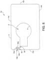
- FIG. 8illustrates an object that is not part of the invention, namely a card core 2c including a straight line discontinuity 44.
- the card core 2cis similar to the card cores 2-2b described above, and similar description is not repeated herein.
- the card core 2creplaces the sinuous line discontinuity 10 with a straight line discontinuity 44 extending from an edge 9 of the cutout 8 to an edge 12a of the card core 2c.
- the straight line discontinuity 44includes a thickness selected to effectively isolate a first side 20a of the discontinuity 44 from a second side 20b without substantially weakening the structure of the card core 2.
- the straight line discontinuity 44includes a width (e.g., distance from first side 20a to second side 20b) of at least 300 microns, at least 500 microns, at least 700 microns, 300-900 microns, and/or any other suitable width.
- FIG. 9illustrates an object that is not part of the invention, namely a card core 2d including a cutout 58 extending to an edge 14a of the card core 2d.
- the card core 2dis substantially similar to the card core 2 described above, and similar description is not repeated herein.
- the card core 2dincludes a body 52 defining a cutout 58 including a first portion 58a and a second portion 58b.
- the body 52extends substantially defined by a first short edge 12a, a second short edge 12b, a first long edge 14a, and a second long edge 14b.
- the cutout 58extends from the first long edge 14a into the body 52 such that the cutout 58 defines a portion of the first long edge 14a of the card.
- one or more circuit elementsmay be positioned within any portion of the cutout 58 such that a gap (see FIGS. 2-3 ) sufficient to electrically isolate the circuit element from the card core 2d is maintained.
- the cutout 58includes a first portion 58a having a first rectangular geometry extending between a first edge portion 60a of the card core 2d and a second edge portion 60b and a second portion 58b having a second rectangular geometry continuous with the first portion 58a.
- the cutout 58can include any number of portions defining any number of geometries, and such embodiments are within the scope of this disclosure.
- a portion of the cutout 58defines an embossable area 62.
- the embossable area 62includes a portion of a card core 2d and/or a finished credential card including the card core 2d that may be subjected to known embossing techniques.
- FIG. 10illustrates a finished credential card 70 (i.e., a credit card) including an overlay layer 72 and an embossing 74 disposed within the embossable area 62.
- FIG. 10further illustrates a circuit element 76, such as a direct contact SoC element, disposed within the second portion 58b of the cutout 58.
- the finished credential card 70may be formed using any known technique, such as, for example, the method 100 discussed above in conjunction with FIG. 4 .
Landscapes
- Engineering & Computer Science (AREA)
- Physics & Mathematics (AREA)
- Computer Hardware Design (AREA)
- Microelectronics & Electronic Packaging (AREA)
- General Physics & Mathematics (AREA)
- Theoretical Computer Science (AREA)
- Electromagnetism (AREA)
- Credit Cards Or The Like (AREA)
Description
- This application relates to a metal card core to be used in a credential card. It also relates to a credential card comprising such a metal card core. It further relates to a method of forming such a credential card.
- Information carrying cards provide identification, authentication, data storage and application processing. Such cards or parts include key cards, identification cards, telephone cards, credit cards, bankcards, tags, bar code strips, other smart cards and the like.
- Current information carrying cards use plastic or other polymer material cores. Current materials fail to provide a desired tactile response and strength. For example, information carrying cards need to withstand flexing to protect identifying components from damage as well as offer good durability during use. In addition, information carrying cards should be appealing, in terms of appearance and feel, to the end user, in order to facilitate use and adoption of the information carrying card. The use of conductive materials for information carrying cards has been disfavored due to coupling (i.e., inductive, conductive, etc.) between circuit elements and the conductive material when used to form an information carrying card.
US2015/021403 discloses a conductive coupling frame having two ends, forming an open loop having two ends and disposed surrounding and closely adjacent a transponder chip module, with an antenna structure in the transponder chip module. In particular, a metal card body with a discontinuous metal layer has a straight slit extending from a module opening, in which a transponder chip module is positioned, to a periphery of the card body to function such as a coupling frame. The previously mentioned slit may have a zigzag geometry.US2016/365644 discloses a similar teaching. - An object of the invention is a metal card core according to claim 1.
- Another object of the invention is a credential card according to claim 12.
- Another object of the invention is a method according to claim 15.
- Aspects of the present disclosure are best understood from the following detailed description when read with the accompanying figures. It is noted that, in accordance with the standard practice in the industry, various features are not drawn to scale. In fact, the dimensions of the various features may be arbitrarily increased or reduced for clarity of discussion.
FIG. 1 illustrates a front view of a card core of a dual interface card defining a cutout and a sinuous line discontinuity, in accordance with some embodiments.FIG. 2 illustrates the card core ofFIG. 1 including a first circuit element positioned in a first portion of the cutout and contact pads formed in a second portion of the cutout, in accordance with some embodiments.FIG. 3 illustrates a front view of the card core ofFIG. 2 having a second circuit element coupled to the contact pads formed in the second portion of the cutout, in accordance with some embodiments.FIG. 4 is a flowchart illustrating a method of forming a credential card including a card core, in accordance with some embodimentsFIG. 5 illustrates a cross-sectional view of a credential core including the card core ofFIG. 2 and a thermoplastic layer disposed on a first side of the card core, in accordance with some embodiments.FIG. 6 illustrates a card core having a sinuous line discontinuity including a first straight line segment and a second straight line segment defining a single flexible finger, in accordance with some embodiments.FIG. 7 illustrates a card core having an sinuous line discontinuity including an extended straight line portion and a truncated straight line portion, in accordance with some embodiments.FIG. 8 illustrates a card core having a straight line discontinuity, the object of this figure being not part of the invention.FIG. 9 illustrates a card core defining a cutout including a portion extending from a first edge of the card core, the object of this figure being not part of the invention.FIG. 10 illustrates a finished credential card incorporating the card core ofFIG. 9 .- The present disclosure generally relates to a dual interface metal card having a current notch formed therein to reduce eddy currents generated in a metal card core. The dual interface metal card has a circuit core positioned between a first metal portion and a second metal portion. The first and second metal portions each define a cutout, such as an antenna cutout. The first and second metal portions further define a discontinuity extending from the cutout to a first edge of the metal card core.
FIG. 1 illustrates acard core 2 of a dual interface card, in accordance with some embodiments. Thecard core 2 includes abody 4. In the illustrated embodiment, thebody 4 includes a generally rectangular shape defined by a plurality ofshort edges long edges metal core 2 can include any suitable shape, such as any suitable regular or irregular geometric shape (e.g., square, rectangle, circle, trapezoid, rhombus, triangle, etc.). Thebody 4 may include any suitable material, such as a metal material, a partially metal material, a conductive non-metal material, a non-conductive non-metal material, and/or any other suitable material. The body material may be selected to provide one or more predetermined features, such as a feel, strength, resiliency, harmonic, and/or other feature, to a card formed using thecard core 2. Example materials include, but are not limited to, stainless steel, tungsten, spring steel, etc. In some embodiments, thebody 4 may include a combination of conductive and non-conductive materials. Example non-conductive materials include, but are not limited to, wood, ceramics, non-conductive plastics, etc.- In some embodiments, the
body 4 defines a void orcutout 8. Thecutout 8 may include multiple portions each having separate geometries. For example, in the illustrated embodiment, thecutout 8 includes afirst portion 8a defined by a circular opening in thebody 4 and asecond portion 8b defined by a square opening in thebody 4, although it will be appreciated that each of thecutout portions FIG. 1 , in some embodiments, two or morecutout portions first cutout portion 8a is continuous with thesecond portion 8b. In some embodiments, thecutout 8 is positioned adjacent to a firstshort edge 12a of thecard core 2. - In some embodiments, the
body 4 may define a plurality ofcutouts 8 each having one or more portions. The plurality ofcutouts 8 may be spaced about thebody 4 such that each of the cutouts is separated by a portion of thebody 4. For example, in some embodiments, thebody 4 may define afirst cutout 8 as illustrated inFIG. 1 and a second cutout (not shown) located adjacent to a secondshort edge 12b of thebody 4. Although the card core embodiments discussed herein include asingle cutout 8 defining multiple portions, it will be appreciated that the various structures, systems, and methods disclosed herein apply equally to card cores having multiple cutouts and are within the scope of this disclosure and the appended claims. - Each
portion cutout 8 may be sized and configured to receive a circuit element therein. Eachportion cutout 8 defines an opening such that the circuit element positioned within thecutout 8 can be effectively electromagnetically isolated from the surrounding material of thebody 4. The effective spacing or gap 26 (seeFIG. 2 ) between a circuit element and theedge 9 of thecutout 8 may vary based on the circuit element positioned within the cutout 8 (or aportion cutout 8 may be spaced at least 300 microns, at least 500 microns, at least 700 microns, and/or any other suitable spacing from theedge 9 of thecutout 8 to effectively isolate a circuit element positioned within thecutout 8 from the material of thebody 4. It will be appreciated that the spacing may be larger and/or smaller based on the circuit element positioned within thecutout 8 and/or properties of the card core 2 (for example, based on the material of the card core 2). - The
body 4 defines asinuous line discontinuity 10 extending from an outer edge (such as firstshort edge 12a) of thebody 4 to an inner edge of thecutout 8. Thesinuous line discontinuity 10 includes a break or channel in thebody 4 such that a continuous circular path does not exist within thebody 4 that extends around thecutout 8. Thesinuous line discontinuity 10 can include any suitable gap within thebody 4 sufficient to effectively prevent electromagnetic coupling between afirst edge 20a and asecond edge 20b of thebody 4 defining thesinuous line discontinuity 10. For example, in some embodiments, thesinuous line discontinuity 10 includes a channel having a width of about 300-900 microns, at least 300 microns, at least 500 microns, at least 700 microns, up to 1000 microns, up to 2000 microns, etc., although it will be appreciated that discontinuities of greater and/or lesser size can be used and are within the scope of this disclosure. - In some embodiments, the
sinuous line discontinuity 10 defines a plurality offlexible fingers flexible finger 22a and a secondflexible finger 22b. theflexible fingers body 4 when a force is applied to a card including thecard core 2. For example, and as discussed in greater detail below, thecard core 2 may be incorporated into a credential card, such as a credit card, biometric card, etc. The credential card may include a plurality of additional layers and/or materials, such as, for example, thermoplastic layers, adhesive layers, polymer layers, etc. The length and width of each of theflexible fingers sinuous line discontinuity 10 provides a flex profile similar to the solid portions of a finished credential card. Theflexible fingers sinuous line discontinuity 10. - The
sinuous line discontinuity 10 and theflexible fingers card core 2 to allow bending in the finished credential card. Thesinuous line discontinuity 10 and theflexible fingers sinuous line discontinuity 10 prevents card stress and breakage by distributing the surface area and torque pressure of an applied force evenly across the finished credential card (and the card core 2), avoiding cracking and/or breakage in a finished credential card or similar card containing thecard core 2. - In some embodiments, the
flexible fingers flexible finger body 4. For example, in some embodiments, the eachflexible finger body 4. The flex profile of each of theflexible fingers card core 2 therein. In some embodiments, the flex profile is selected such that eachflexible finger sinuous line discontinuity 10 as would be provided by a solid portion of thebody 4 positioned in the same location, although it will be appreciated that eachflexible finger - In some embodiments, the sinuous line discontinuity is configured to reduce and/or eliminate eddy currents generated in the
body 4 during operation. For example, in some embodiments, exposure of acard core 2 comprising a metallic, semi-metallic, or other conductive material to one or more electromagnetic signals typically generates one or more eddy currents in theconductive body 4. Eddy currents flow in a closed loop within the conductor (e.g., body 4). The sinuous line discontinuity eliminates any conductive loop around thecutout 8 and effectively reduces the area available for eddy currents. The sinuous line discontinuity effectively reduces and/or eliminates eddy currents (and other signals) generated in and/or by thebody 4. Although a single sinuous line discontinuity is illustrated, it will be appreciated that acard core 2 can include a plurality ofcutouts 8 each having one ormore discontinuities 10 extending from anouter edge body 4. - In some embodiments, the
sinuous line discontinuity 10 includes a plurality ofcurved portions 34a-34d coupled by a plurality of substantiallystraight portions 36a-36c. The plurality of substantiallystraight portions 36a-36c each extend substantially parallel to each other over a predetermine length of thecard core 2. In some embodiments, thesinuous line discontinuity 10 defines a smooth, repetitive oscillating curve (e.g., a sinusoidal curve), although it will be appreciated that thediscontinuity 10 can include sharp (e.g., non-smooth) curved portions and/or non-parallel portions and suchsinuous line discontinuity 10 is within the scope of this disclosure. In various embodiments, thecard core 2 can include a plurality ofcutouts 8 each having at least onesinuous line discontinuity 10 extending from an inner edge of thecutout 9 to anouter edge 12b body 4. - For example, in the illustrated embodiment, the
sinuous line discontinuity 10 includes afirst portion 38 extending from thecutout 8, a plurality of substantiallystraight portions 34a-34c extending at a non-parallel angle with respect to thefirst portion 38, a plurality ofcurved portions 32a-32d coupling the substantiallystraight portions 34a-34cm each having a predetermined curvature over a predetermined area, and ansecond portion 40 extending at a predetermined angle with respect to the substantiallystraight portions 36a-36c to afirst edge 12a of thecard core 2. It will be appreciated that thecurved portions 32a-32d can include any suitable curvature, such as, for example, any curvature between 45°-315°, 135°-225°, 160°-200°, 90°-270° and/or any other suitable curvature. It will be appreciated that the acard core 2 can include additional and/or different discontinuities, for example, as illustrated inFIGS. 5-6 . - The
cutout 8 and/or thesinuous line discontinuity 10 may be formed using any suitable method. For example, in various embodiments, thecutout 8 and/or thesinuous line discontinuity 10 may be formed using one or more of a milling technique, an etching technique, a molding technique, and/or any other suitable technique. It will be appreciated that thecutout 8 and thesinuous line discontinuity 10 may be formed using the same and/or different techniques. In some embodiments, thesinuous line discontinuity 10 is formed in thecard core 2 prior to thecard core 2 receiving any circuit elements within thecutouts 8. FIGS. 2 and3 illustrate thecard core 2 ofFIG. 1 having a plurality of circuit elements positioned within thecutout 8, in accordance with some embodiments. As shown inFIG. 2 , in some embodiments, afirst circuit element 16a, such as anantenna 18, may be positioned within afirst portion 8a of acutout 8. Theantenna 18 includes a plurality of concentric wire coils. Theantenna 18 can include any suitable antenna, such as a printed antenna including one or more circular coils. Although a generally circular antenna is illustrated, it will be appreciated by those skilled in the art that theantenna 18 can have any suitable shape and/or any suitable number of windings (or coils). In some embodiments, thefirst circuit element 16a can include a minimum thickness, such as, for example, a thickness between 50 and 100 microns, between 75 and 90 microns, and/or any other suitable thickness. The thickness of thefirst circuit element 16a may be less than, greater than, and/or equal to the thickness of thecard core 2.- The
first circuit element 16a is positioned within thefirst cutout portion 8a such that agap 26 is maintained between theedge 9 of thecutout 8 and the outer edge of thefirst circuit element 16a. For example, in the illustrated embodiment, theantenna 8 is positioned to ensure agap 26 suitable gap, such as at least 300 microns, at least 500 microns, at least 700 microns, 300-900 microns, up to 1000 microns, up to 2000 microns, and/or any other suitable gap is maintained between an outer coil of theantenna 18 and theedge 9. Although specific embodiments are discussed herein with respect to the illustrated circuit elements, it will be appreciated that thegap 26 can include any gap sufficient to electromagnetically isolate thefirst circuit element 16a from the material of thebody 4. - In some embodiments, the
gap 26 is selected based on one or more dimensions of thecard core 2 and/or a credential card formed from thecard core 2. For example, in some embodiments, thegap 26 is a distance equal to at least the width of a finished credential card formed using thecard core 2. A finished credential card may have any thickness sufficient to contain thecard core 2, one or more circuit elements positioned within thecutout 8, and/or any additional layers formed around thecard core 2. For example, a finished credential card may have a thickness of at least 700 microns, at least 750 microns, at least 800 microns, etc. - In some embodiments, the
first circuit element 16a is coupled to a plurality ofcontact pads second cutout portion 8b of the cutout by a plurality ofleads contact pads FIG. 3 ), positioned within thesecond cutout portion 8b, to thefirst circuit element 16a. Thecontact pads second cutout portion 8b to allow the second circuit element 16b to be coupled to thecontact pads FIG. 3 ) between theedge 9 of thecutout 8 and the second circuit element 16b. In some embodiments, thecontact pads first circuit element 16a. - In some embodiments, the
first circuit element 16a, thecontact pads leads FIG. 5 ). The supportingfilm 17 is sized and configured to be received within thecutout 8 while maintain thepredetermined gaps circuit elements 16a, 16b and theedge 9 of thecutout 8. Thefirst circuit element 16a, thecontact pads leads film 17 using any suitable formation method. For example, in some embodiments, thefirst circuit element 16a, thecontact pads leads film 17 using a process to print conductive traces and/or other materials. Although embodiments are discussed herein including printed circuit elements, it will be appreciated that thefirst circuit element 16a, thecontact pads leads FIG. 3 illustrates thecard core 2 ofFIG. 2 having a second circuit element 16b positioned within asecond portion 8b of thecutout 8. The second circuit element 16b can include any suitable circuit element, such as, for example, an active circuit element(e.g., a direct contact System-on-Chip (SoC) element) 32. The second circuit element 16b may be positioned over and coupled to thecontact pads second cutout 8b. The second circuit element 16b is electromagnetically isolated from thebody 4 of thecard core 2. For example, in the illustrated embodiment, the directcontact SoC element 32 is limited to direct contact coupling between theSoC element 32 and theantenna 18 and does not include any inductive coupling elements, effectively isolating theSoC element 32 from the material of thebody 4. In some embodiments, the second circuit element 16b may be positioned a predetermined distance from theedge 9 of thecutout 8 such that a second circuit element 16b capable of inductive, conductive, or other contactless coupling is effectively isolated from the material of thebody 4.- In some embodiments, the
contact pads first circuit element 16a are maintained in a co-planar relationship (i.e., are parallel with respect to a plane defined by the body 4). When thecontact pads first circuit element 16a are co-planar, a second circuit element 16b coupled to thecontact pads first circuit element 16a. In such embodiments, the second circuit element 16b is coupled to thefirst circuit element 16a only through theleads first circuit element 16a. - In some embodiments, the second circuit element 16b includes a second antenna (not shown). The second antenna can have a different configuration as compared to the antenna 16 (e.g., greater and/or lesser antenna area, larger/smaller material, different shape, etc.) such that the second antenna produce different responses as compared to the antenna 16 when each is simultaneously exposed to the same electromagnetic signal.
- In some embodiments, the
card core 2 and the plurality ofcircuit elements 16a, 16b positioned within thecutout 8 can be coupled between one or more additional layers, materials, and/or surfaces to form a credential core and/or a finished credential card (e.g., a credit/debit card, and ATM or bank card, an identification card, a state issued license or identification (e.g., driver's license), a security badge, a loyalty card, biometric card, etc.). The additional layers can include any suitable materials, such as, for example, metal, plastic, vinyl, and/or other materials. FIG. 4 is a flowchart illustrating amethod 100 of forming a credential card including acard core 2, in accordance with some embodiments. At step 102, acard core 2 including abody 4 defining at least onecutout 8 is formed. Thecard core 2 can be formed using any suitable technique, such as, for example, pressing, stamping, milling, molding, etc. In some embodiment, thebody 4 is formed defining thecutout 8. In other embodiments, a solid body is formed and thecutout 8 is subsequently formed in the solid body using any suitable technique, such as, for example, milling, drilling, etching, cutting, etc.- At step 104, a
sinuous line discontinuity 10 is formed in thebody 4 extending from afirst edge 12a of thebody 4 to thecutout 8. Thesinuous line discontinuity 10 can be formed using any suitable technique, such as, for example, etching, stamping, laser cutting, mechanical cutting (milling or other mechanical/contact cutting), water-jet cutting, etc. Thesinuous line discontinuity 10 includes one ormore curves straight line segments 36a-36c. In some embodiments, thestraight line segments 36a-36c are parallel and define a plurality offingers body 4. - At
optional step 106, asurface 5 of thebody 4 may be treated to form one or more patterns and/or images on the surface. For example, in some embodiments, the surface of thebody 4 may be etched, milled, and/or otherwise processed to form a predetermined pattern, images, pictures, symbols, trademarks, words, pictograms, or other visual indicators. In some embodiments, at least a portion of thesurface 5 may be colorized using any suitable colorization process, such as, for example, inking, printing, sintering, etc. The colorization may be in combination with and/or alternative to the formation of one or more patterns or images through surface treatment. Although steps 102-106 are illustrated as separate steps, it will be appreciated that steps 102-106 may be integrated into and/or performed simultaneously one or more of steps 102-106, and each combination is within the scope of this disclosure. - At step 108, one or more circuit elements are positioned within the
cutout 8 defined in thecard core 2. For example, in some embodiments, afirst circuit element 16a, a plurality ofcontact pads leads first circuit element 16a, a plurality ofcontact pads leads cutout 8 such that afirst gap 26 is defined between thefirst circuit element 16a and theedge 9 of thecutout 8 to effectively electromagnetically isolate thefirst circuit element 16a from the material of thebody 4. The circuit core and/or the individual circuit elements may be positioned using any suitable method, such as, for example, by hand, by a pick-and-place method, and/or using any other suitable method. In some embodiments, a second circuit element 16b may be positioned within thecutout 8, for example, within asecond portion 8b of thecutout 8 simultaneous with the placement of thefirst circuit element 16a and/or thecontact pads - At
step 110, acredential core 200 including thecard core 2 is formed. The credential core may be formed by coupling athermoplastic layer 80 on a first side of thecard core 2, as illustrated inFIG. 5 . Thethermoplastic layer 80 may be simultaneously coupled to thecard core 2 and/or thecircuit elements 16a positioned therein so as to form acredential core 200. In some embodiments, thethermoplastic layer 80 is coupled to thecard core 2 at a predetermined pressure and/or at a predetermined temperature. Thethermoplastic layer 80 may include any suitable material, such as, for example, a moly-based material (e.g., molybendum), polyvinyl chloride (PVC), a copolymer of vinyl chloride, polyolefin, polycarbonate, polyester, polyamide, acrylonitrile butadiene styrene copolymer (ABS), and the like. Examples of PVC films suitable for use with the invention are available from suppliers such as Klockner Pentaplast of America, Inc. of Gordonsville, VA; and Shijiazhuang Eurochem Co. Ltd of China. Examples of such a vinyl chloride copolymer resin are available from Dow Chemical Company under trade name of UCAR®, and from BASF of Ludwigshafen, Germany under trade name of Laroflex®. In some embodiments, amaterial layer 82 may be positioned between thethermoplastic layer 80 and thecard core 2. Thematerial layer 82 may include any suitable material, such as, for example, a cross-linkable polymer, an adhesive, and/or any other suitable material. Examples of cross-linkable polymers are disclosed inU.S. Patent 9,275,321, granted on March 1, 2016 - At
optional step 112, a credential card may be formed by positioning one or more additional layers above and/or below the credential core formed at step 210. The additional layers may include any suitable materials or layers, such as, for example, image layers, sealing layers, thermoplastic layers, metal layers, conductive layers, non-conductive layers, and/or any other suitable layers. Although embodiments are discussed herein with respect to asingle card core 2, a single credential core, and a single credential card, it will be appreciated thatmultiple card cores 2, credential cores, and/or credential cards may be formed simultaneously using any suitable process. Various processes for forming a credential card compatible with the metal card cores disclosed herein are disclosed in, for example,U.S. Pat. Appl. Pub. No. 2016/0152815, published June 2, 2016 . A credential card including a card core, such as acard core 2, disclosed herein can be formed using any suitable method. For example, in various embodiments, a credential card including acard core 2 may be formed using a cold laminate process, injection molding, milling, laser cutting, water-jet processes, etc. - At optional step 114, a portion of each layer positioned above the
contact pads contact pads contact pads contact pads contact SoC element 32, to be positioned with a surface parallel to a plane defined by a surface of the credential card and/or the card core (as illustrated inFIG. 3 ). FIG. 6 illustrates acard core 2a having asinuous line discontinuity 10a including a firststraight line segment 36a and a secondstraight line segment 36b defining a single flexible finger 22, in accordance with some embodiments. Thecard core 2a is similar to thecard core 2 discussed above, and similar description is not repeated herein. Thesinuous line discontinuity 10a generally defines a curved path (e.g., a notch or channel) extending from an inner edge of thecutout 8 to anouter edge 12a of thecore card 2aFIG. 7 illustrates a card core 2b having asinuous line discontinuity 10b including an extendedstraight line portion 42a and a truncatedstraight line portion 42b, in accordance with some embodiments. The card core 2b is similar to themetal card core 2 discussed above in conjunction withFIG. 5 , and similar description is not repeated herein. The card core 2b includes asinuous line discontinuity 10b coupled to a lower portion of thesecond portion 8b of thecutout 8. A first substantiallystraight portion 42a of thediscontinuity 10b has a longer length as compared to a first substantiallystraight portion 36a of thesinuous line discontinuity 10a of thecard core 2 and a secondstraight portion 42b has a substantially shorter length. Thesinuous line discontinuity 10b further includes afirst portion 38a extending from thecutout 8 and a second portion 38b extending from thefirst edge 12a, each disposed at a non-parallel and non-perpendicular angle with respect to each of theedges FIG. 8 illustrates an object that is not part of the invention, namely a card core 2c including astraight line discontinuity 44. The card core 2c is similar to the card cores 2-2b described above, and similar description is not repeated herein. The card core 2c replaces thesinuous line discontinuity 10 with astraight line discontinuity 44 extending from anedge 9 of thecutout 8 to anedge 12a of the card core 2c. Thestraight line discontinuity 44 includes a thickness selected to effectively isolate afirst side 20a of thediscontinuity 44 from asecond side 20b without substantially weakening the structure of thecard core 2. For example, in various embodiments, thestraight line discontinuity 44 includes a width (e.g., distance fromfirst side 20a tosecond side 20b) of at least 300 microns, at least 500 microns, at least 700 microns, 300-900 microns, and/or any other suitable width.FIG. 9 illustrates an object that is not part of the invention, namely acard core 2d including acutout 58 extending to anedge 14a of thecard core 2d. Thecard core 2d is substantially similar to thecard core 2 described above, and similar description is not repeated herein. Thecard core 2d includes abody 52 defining acutout 58 including afirst portion 58a and asecond portion 58b. Thebody 52 extends substantially defined by a firstshort edge 12a, a secondshort edge 12b, a firstlong edge 14a, and a secondlong edge 14b. Thecutout 58 extends from the firstlong edge 14a into thebody 52 such that thecutout 58 defines a portion of the firstlong edge 14a of the card. As discussed above with respect tocard core 2, one or more circuit elements may be positioned within any portion of thecutout 58 such that a gap (seeFIGS. 2-3 ) sufficient to electrically isolate the circuit element from thecard core 2d is maintained.- In
FIG. 9 , thecutout 58 includes afirst portion 58a having a first rectangular geometry extending between afirst edge portion 60a of thecard core 2d and asecond edge portion 60b and asecond portion 58b having a second rectangular geometry continuous with thefirst portion 58a. Although specific illustration is provided, it will be appreciated that thecutout 58 can include any number of portions defining any number of geometries, and such embodiments are within the scope of this disclosure. - In
FIG. 9 , a portion of thecutout 58, such as thefirst portion 58a, defines an embossablearea 62. The embossablearea 62 includes a portion of acard core 2d and/or a finished credential card including thecard core 2d that may be subjected to known embossing techniques. For example,FIG. 10 illustrates a finished credential card 70 (i.e., a credit card) including anoverlay layer 72 and anembossing 74 disposed within the embossablearea 62.FIG. 10 further illustrates acircuit element 76, such as a direct contact SoC element, disposed within thesecond portion 58b of thecutout 58. The finishedcredential card 70 may be formed using any known technique, such as, for example, themethod 100 discussed above in conjunction withFIG. 4 . - Although the subject matter has been described in terms of exemplary embodiments, it is not limited thereto. Rather, the appended claims define the invention and the claims may be interpreted broadly, to include other variants and embodiments, which may be made by those skilled in the art.
Claims (15)
- A metal card core (2; 2a; 2b) to be used in a credential card, comprising:a body (4) comprising a metal material, the body defining:a cutout (8) that includes an opening in the body, anda discontinuity (10; 10a; 10b) that includes a channel defined by the body and extending from an outer surface (12a, 12b, 14a, 14b) of the body to the cutout; andat least one circuit element (16a, 16b) positioned within the cutout (8),characterized in that the discontinuity comprises a sinuous line discontinuity (10; 10a; 10b) that includes at least one curved portion (34a-34d) and at least one straight line portion (36a-36c; 42a, 42b),andin that the cutout (8) defines a size and geometry such that a gap (26) between the at least one circuit element (16a, 16b) and an edge (9) of the cutout has an effective spacing to electromagnetically isolate the at least one circuit element (16a, 16b) from the metal material of the body (4).
- The metal card core of claim 1, wherein the sinuous line discontinuity (10) defines a plurality of flexible fingers (22a, 22b) configured to provide a flex profile similar to a continuous portion of the body (4) when a force is applied to the metal card core (2).
- The metal card core of claim 1, wherein the sinuous line discontinuity (10a; 10b) includes a first straight line segment (36a) and a second straight line segment (36b) defining a single flexible finger (22).
- The metal card core of claim 1, wherein the at least one curved portion (34a-34d) defines a 180° curve.
- The metal card core of claim 4, wherein the sinuous line discontinuity (10; 10a; 10b) defines a smooth repetitive oscillating curve.
- The metal card core of claim 1, wherein the cutout (8) includes a first portion (8a) having a first geometry defined by the edge (9) of the cutout and a second portion (8b) having a second geometry defined by the edge of the cutout, and wherein the first and second portions (8a, 8b) of the cutout (8) overlap such that the first portion is continuous with the second portion.
- The metal card core of claim 6, wherein the first geometry is circular and the second geometry is square.
- The metal card core of claim 6, wherein a first circuit element (16a) is positioned in the first portion (8a) of the cutout (8) and a second circuit element (16b) is positioned in the second portion (8b) of the cutout.
- The metal card core of claim 8, wherein the first circuit element (16a) is coupled to a plurality of contact pads (24a, 24b) positioned within the second portion (8b) of the cutout (8), and wherein the second circuit element (16b) is coupled to the first circuit element (16a) by the contact pads (24a, 24b).
- The metal card core of claim 9, wherein the first circuit element (16a) is an antenna and the second circuit elements (16b) is a direct-contact System-on-Chip (SoC) element.
- The metal card core of claim 1, wherein the body (4) comprises a conductive non-metal material.
- A credential card, comprising:a metal card core (2; 2a; 2b) according to any one of claims 1 to 11;a first material layer (80, 82) disposed over a first side of the metal card core; anda second material layer disposed over a second side of the metal card core,wherein the first material layer and the second material layer are each coupled to the body (4) of the metal card core in a first region of the credential card, wherein the first material layer is coupled to the second material layer in a second region of the credential card, and wherein the second region is substantially aligned with the cutout (8) of the metal card core.
- The credential card of claim 12, wherein the sinuous line discontinuity (10; 10a; 10b) defines a plurality of flexible fingers (22a, 22b) configured to distribute torque pressure to provide a flex profile similar to the remainder of the credential card, incorporating solid sections of the body (4), to avoid cracking or breaking of any layer of the credential card when a bending pressure is applied to the credential card.
- The credential card of claim 12, wherein the cutout (8) includes a first portion (8a) having a first geometry defined by the edge and a second portion (8b) having a second geometry defined by the edge, wherein the first and second portions (8a, 8b) of the cutout (8) overlap such that the first portion is continuous with the second portion, and wherein the second region is substantially aligned with the first and second portions (8a, 8b) of the cutout (8).
- A method of forming a credential card, comprising:forming a cutout (8) in a body (4) of a metal card core (2; 2a; 2b), wherein the body comprises a metal material, and wherein the cutout includes an opening in the body;forming a sinuous line discontinuity (10; 10a; 10b) in the body, wherein the sinuous line discontinuity includes a channel defined by the body and extending from an outer surface (12a, 12b, 14a, 14b) of the body to the cutout, and wherein the sinuous line discontinuity includes at least one curved portion (34a-34d) and at least one straight line portion (36a-36c; 42a, 42b);positioning at least one circuit element (16a, 16b) within the cutout, wherein the cutout defines a size and geometry such that a gap (26) between the at least one circuit element and an edge (9) of the cutout has an effective spacing to electromagnetically isolate the at least one circuit element from the metal material of the body;positioning a thermoplastic material layer (80, 82) over a first side of the metal card core; andcoupling the thermoplastic material layer to the body of the card core in a first region and the thermoplastic material layer to the at least one circuit element in a second region, wherein the second region is substantially aligned with the cutout.
Applications Claiming Priority (2)
| Application Number | Priority Date | Filing Date | Title |
|---|---|---|---|
| US201862639535P | 2018-03-07 | 2018-03-07 | |
| PCT/US2019/020919WO2019173455A1 (en) | 2018-03-07 | 2019-03-06 | Metal card |
Publications (3)
| Publication Number | Publication Date |
|---|---|
| EP3762871A1 EP3762871A1 (en) | 2021-01-13 |
| EP3762871A4 EP3762871A4 (en) | 2021-11-10 |
| EP3762871B1true EP3762871B1 (en) | 2024-08-07 |
Family
ID=67846808
Family Applications (1)
| Application Number | Title | Priority Date | Filing Date |
|---|---|---|---|
| EP19763342.3AActiveEP3762871B1 (en) | 2018-03-07 | 2019-03-06 | Metal card |
Country Status (4)
| Country | Link |
|---|---|
| US (4) | US11361204B2 (en) |
| EP (1) | EP3762871B1 (en) |
| CN (1) | CN111819577B (en) |
| WO (1) | WO2019173455A1 (en) |
Families Citing this family (13)
| Publication number | Priority date | Publication date | Assignee | Title |
|---|---|---|---|---|
| US20210081743A1 (en) | 2019-08-12 | 2021-03-18 | Federal Card Services, LLC | Dual interface metal cards and methods of manufacturing |
| US12277462B2 (en) | 2019-08-14 | 2025-04-15 | Federal Card Services, LLC | Metal-containing dual interface smartcards |
| US11416728B2 (en) | 2019-08-15 | 2022-08-16 | Federal Card Services, LLC | Durable dual interface metal transaction cards |
| US11113593B2 (en) | 2019-08-15 | 2021-09-07 | Federal Card Services; LLC | Contactless metal cards with fingerprint sensor and display |
| US11455507B2 (en) | 2019-10-13 | 2022-09-27 | Federal Card Services, LLC | Metal transaction cards containing ceramic having selected coloring and texture |
| WO2021097208A1 (en)* | 2019-11-16 | 2021-05-20 | Federal Card Services, LLC | Rfid enabled metal transaction card with shaped opening and shaped slit |
| US11341385B2 (en) | 2019-11-16 | 2022-05-24 | Federal Card Services, LLC | RFID enabled metal transaction card with shaped opening and shaped slit |
| FR3105856B1 (en)* | 2019-12-31 | 2022-05-06 | Idemia France | Metal smart card suitable for contactless operation |
| USD1032613S1 (en) | 2020-02-02 | 2024-06-25 | Federal Card Services, LLC | Smart card |
| US11551050B2 (en) | 2020-11-12 | 2023-01-10 | Advanide Holdings Pte. Ltd. | Card inlay for direct connection or inductive coupling technology |
| EP4002210A1 (en) | 2020-11-12 | 2022-05-25 | AdvanIDe Holdings Pte. Ltd. | Card inlay for direct connection or inductive coupling technology |
| US12159180B1 (en) | 2021-11-29 | 2024-12-03 | Metaland Llc | RFID enabled metal transaction cards with coupler coil couplings and related methods |
| US12430531B2 (en)* | 2023-01-03 | 2025-09-30 | Giesecke+Devrient ePayments GmbH | Method of manufacturing a card-shaped data carrier and lamination plate therefor |
Family Cites Families (301)
| Publication number | Priority date | Publication date | Assignee | Title |
|---|---|---|---|---|
| US2890202A (en) | 1953-07-20 | 1959-06-09 | Pittsburgh Plate Glass Co | Method of preparing acrylate esters of epoxy resins |
| US3024216A (en) | 1958-07-28 | 1962-03-06 | Union Carbide Corp | Compositions of partially hydrolyzed vinyl chloride-vinyl acetate copolymers and polyurethane resins, polyethylene coated with same and process for making coated article |
| US3191788A (en) | 1963-03-26 | 1965-06-29 | Grand Specialties Company | Load tilting mechanism for industrial truck |
| US3847654A (en) | 1970-06-08 | 1974-11-12 | M & T Chemicals Inc | Substrate bonded with vinyl dispersion textured coating |
| JPS5271590A (en) | 1975-12-01 | 1977-06-15 | Bridgestone Corp | Production of novel high polymer |
| US4115479A (en) | 1976-08-11 | 1978-09-19 | Vynacron Dental Co. | Casting resins by polymerizing liquid monomer in mixture of particulated vinyl halide resins |
| DE2837435B2 (en) | 1978-08-28 | 1981-06-25 | Friedrich Horst 5840 Schwerte Papenmeier | Process and device for processing PVC powder |
| DE2920012C2 (en)* | 1979-05-17 | 1988-09-29 | GAO Gesellschaft für Automation und Organisation mbH, 8000 München | Identification card with IC component and method for producing such an identification card |
| US4310451A (en) | 1979-10-25 | 1982-01-12 | Diamond Shamrock Plastics Corporation | Free flowing rigid PVC resin powder compositions |
| DE3131216C3 (en) | 1981-04-14 | 1994-09-01 | Gao Ges Automation Org | ID card with IC module |
| US4382201A (en) | 1981-04-27 | 1983-05-03 | General Electric Company | Ultrasonic transducer and process to obtain high acoustic attenuation in the backing |
| US4480079A (en) | 1982-04-12 | 1984-10-30 | Imperial Chemical Industries Plc | Copolymerization of unsaturated urethane monomers |
| US4399061A (en) | 1981-10-14 | 1983-08-16 | Rca Corporation | Preparation of video disc molding composition |
| DE3248385A1 (en) | 1982-12-28 | 1984-06-28 | GAO Gesellschaft für Automation und Organisation mbH, 8000 München | ID CARD WITH INTEGRATED CIRCUIT |
| US4463128A (en) | 1983-05-09 | 1984-07-31 | W. R. Grace & Co. | Reactive plastisol dispersion |
| JPS60252992A (en) | 1984-05-30 | 1985-12-13 | Toshiba Corp | Ic card |
| FR2570101B1 (en) | 1984-09-07 | 1987-09-25 | Sotimag | ANTI-FRAUD PROCESS FOR VALUE DOCUMENTS |
| DE3575965D1 (en) | 1984-12-19 | 1990-03-15 | Soil Machine Dynamics Ltd | METHOD AND DEVICE FOR LIFTING GROUND. |
| EP0189987B1 (en) | 1985-01-25 | 1992-04-29 | Imperial Chemical Industries Plc | Polymerisable urethane compositions |
| DE8504263U1 (en) | 1985-02-15 | 1986-06-12 | Schwan-Stabilo Schwanhäußer GmbH & Co, 8500 Nürnberg | Powder leads for cosmetic pencils |
| DE3519053A1 (en) | 1985-05-28 | 1986-12-18 | W.R. Grace & Co., Cambridge, Mass. | CAULK |
| JPH0686177B2 (en) | 1986-09-29 | 1994-11-02 | 河西工業株式会社 | Interior parts for automobiles |
| GB8624082D0 (en) | 1986-10-08 | 1986-11-12 | Dunlop Cct Sa | Vinyl chloride polymer products |
| JPS63141790A (en)* | 1986-12-03 | 1988-06-14 | 菱電化成株式会社 | Identification card |
| JPS63185630A (en) | 1987-01-29 | 1988-08-01 | 東洋鋼板株式会社 | Manufacture of steel plate coated with high-hardness vinyl chloride |
| US4775698A (en) | 1987-04-14 | 1988-10-04 | The B. F. Goodrich Company | Process for producing porous substantially skinless particles of crosslinked PVC resin |
| US4742085A (en) | 1987-04-14 | 1988-05-03 | The B. F. Goodrich Company | Crosslinked porous skinless particles of PVC resin and process for producing same |
| US4775702A (en) | 1987-04-14 | 1988-10-04 | The B. F. Goodrich Company | Inversion process for producing low-skin porous friable particles of crosslinked PVC resin |
| US4775700A (en) | 1987-04-14 | 1988-10-04 | The B. F. Goodrich Company | Process for producing porous skinless particles of crosslinked PVC resin |
| US4775699A (en) | 1987-04-14 | 1988-10-04 | The B. F. Goodrich Company | Crosslinked porous skinless particles of PVC resin |
| US4775701A (en) | 1987-04-14 | 1988-10-04 | The B. F. Goodrich Company | Mass process for producing porous friable particles of crosslinked PVC resin |
| DE68912426T2 (en) | 1988-06-21 | 1994-05-11 | Gec Avery Ltd | Manufacture of portable electronic cards. |
| KR970005475B1 (en) | 1988-07-15 | 1997-04-16 | 클레리언트 파이넌스(비브이아이) 리미티드 | Method for producing polylactones and corresponding salts of poly- [α-hydroxy- (acrylic, croton, or acryl + croton) acid] |
| US5084501A (en) | 1988-11-07 | 1992-01-28 | Armstrong World Industries, Inc. | Highly filled resin powder |
| US5143723A (en) | 1988-11-23 | 1992-09-01 | Estee Lauder, Inc. | Colored cosmetic compositions |
| US5324506A (en) | 1988-11-23 | 1994-06-28 | Estee Lauder, Inc. | Colored cosmetic compositions |
| US4954195A (en) | 1989-02-13 | 1990-09-04 | Lockheed Corporation | Production of thermoset composites containing thermoplastic fillers |
| US5084699A (en) | 1989-05-26 | 1992-01-28 | Trovan Limited | Impedance matching coil assembly for an inductively coupled transponder |
| ES2088781T3 (en) | 1990-01-19 | 1996-09-16 | Minnesota Mining & Mfg | THERMOSURING COMPOSITION. |
| JPH03239595A (en) | 1990-02-16 | 1991-10-25 | Dainippon Printing Co Ltd | Manufacture of card |
| NL9000840A (en) | 1990-04-10 | 1991-11-01 | Wavin Bv | METHOD AND INSTALLATION FOR MANUFACTURING PLASTIC PREPARATIONS USING A HOT PVC POWDER MIXTURE AND ADDITIVES, AND A WARM BLENDER SUITABLE FOR USE IN THIS METHOD |
| US5198501A (en) | 1990-08-20 | 1993-03-30 | Air Products And Chemicals, Inc. | In-situ polymerized blends of vinyl acetate/ethylene copolymar and poly(vinyl chloride) |
| JPH04216850A (en) | 1990-12-17 | 1992-08-06 | Nippon Zeon Co Ltd | Polyvinyl chloride plastisol composition |
| USD341092S (en) | 1991-04-08 | 1993-11-09 | Manufacture Jaeger-Le Coultre, S.A. | Wrist watch |
| US5281855A (en) | 1991-06-05 | 1994-01-25 | Trovan Limited | Integrated circuit device including means for facilitating connection of antenna lead wires to an integrated circuit die |
| DE4135937C2 (en) | 1991-10-31 | 1997-07-03 | Pegulan Tarkett Ag | Process for making latex, PVC, and plasticizer-free textile or plastic floor and wall coverings |
| US5233022A (en) | 1991-08-26 | 1993-08-03 | United Technologies Automotive, Inc. | Flow property shelf life of PVC dry blend powders |
| US5198170A (en) | 1991-09-19 | 1993-03-30 | The B. F. Goodrich Company | Method for extrusion of powered PVC compounds |
| JP3049894B2 (en) | 1991-11-27 | 2000-06-05 | 日本ゼオン株式会社 | Acrylic ester copolymer plastisol composition |
| US5255430A (en) | 1992-10-08 | 1993-10-26 | Atmel Corporation | Method of assembling a module for a smart card |
| FR2701268B1 (en) | 1993-02-05 | 1995-04-14 | Atochem Elf Sa | Powder-based polyamide paints for coating PVC profiles. |
| US5407893A (en) | 1993-08-19 | 1995-04-18 | Konica Corporation | Material for making identification cards |
| JPH0793817A (en) | 1993-09-24 | 1995-04-07 | Canon Inc | Information recording medium |
| FR2713648B1 (en) | 1993-12-15 | 1996-03-01 | Rhone Poulenc Chimie | Stabilizing composition for chlorinated polymer comprising beta-diketones. |
| FR2716555B1 (en) | 1994-02-24 | 1996-05-15 | Gemplus Card Int | Method of manufacturing a contactless card. |
| DE69530922T2 (en) | 1994-03-31 | 2003-12-24 | Ibiden Co. Ltd., Ogaki | DEVICE WITH ELECTRONIC COMPONENT |
| JPH0817288A (en) | 1994-07-04 | 1996-01-19 | Matsushita Electric Ind Co Ltd | Transparent touch panel |
| FR2724477B1 (en) | 1994-09-13 | 1997-01-10 | Gemplus Card Int | NON-CONTACT CARD MANUFACTURING PROCESS |
| EP0766197A4 (en) | 1995-04-13 | 1999-12-29 | Dainippon Printing Co Ltd | Ic card and ic module |
| USD378064S (en) | 1995-05-11 | 1997-02-18 | Manufacture Jaeger-Le Coultre Sa | Wristwatch |
| US6611199B1 (en) | 1995-10-11 | 2003-08-26 | Motorola, Inc. | Capacitively powered portable communication device and associated exciter/reader and related method |
| KR100373063B1 (en) | 1996-02-12 | 2003-05-12 | 만프레트 리츨러 | Wire conductor connection method and device |
| CA2245775C (en) | 1996-02-12 | 2004-04-06 | David Finn | Method and device for bonding a wire conductor |
| FR2761497B1 (en) | 1997-03-27 | 1999-06-18 | Gemplus Card Int | METHOD FOR MANUFACTURING A CHIP CARD OR THE LIKE |
| FR2762115B1 (en) | 1997-04-10 | 1999-12-03 | Schlumberger Ind Sa | METHOD FOR INSERTING AN ELECTRONIC MODULE INTO AN ELECTRONIC MEMORY CARD BODY |
| US5955021A (en) | 1997-05-19 | 1999-09-21 | Cardxx, Llc | Method of making smart cards |
| NO310365B1 (en) | 1997-07-18 | 2001-06-25 | Norsk Hydro As | PVC mixture, its use and method for its preparation |
| US6052062A (en) | 1997-08-20 | 2000-04-18 | Micron Technology, Inc. | Cards, communication devices, and methods of forming and encoding visibly perceptible information on the same |
| FR2769110B1 (en) | 1997-09-26 | 1999-12-03 | Gemplus Card Int | METHOD FOR MANUFACTURING AN ELECTRONIC MODULE OR LABEL, MODULE OR LABEL OBTAINED AND SUPPORT COMPRISING SUCH A MODULE OR LABEL |
| US6037879A (en) | 1997-10-02 | 2000-03-14 | Micron Technology, Inc. | Wireless identification device, RFID device, and method of manufacturing wireless identification device |
| US7012504B2 (en) | 2002-04-01 | 2006-03-14 | Micron Technology, Inc. | Wireless identification device, RFID device with push-on/push off switch, and method of manufacturing wireless identification device |
| US6768415B1 (en) | 1997-10-03 | 2004-07-27 | Micron Technology, Inc. | Wireless identification device, RFID device with push-on/push-off switch, method of manufacturing wireless identification device |
| CN1179295C (en) | 1997-11-14 | 2004-12-08 | 凸版印刷株式会社 | Composite IC module and composite IC card |
| USD404319S (en) | 1997-12-24 | 1999-01-19 | Manufacture Jaeger-Le Coultre Sa | Wristwatch |
| BR9908016A (en) | 1998-02-17 | 2000-10-24 | Du Pont | Process for the production of powder finishes |
| US6241153B1 (en) | 1998-03-17 | 2001-06-05 | Cardxx, Inc. | Method for making tamper-preventing, contact-type, smart cards |
| US6353242B1 (en) | 1998-03-30 | 2002-03-05 | Kabushiki Kaisha Toshiba | Nonvolatile semiconductor memory |
| US6191382B1 (en) | 1998-04-02 | 2001-02-20 | Avery Dennison Corporation | Dynamic laser cutting apparatus |
| US6018299A (en) | 1998-06-09 | 2000-01-25 | Motorola, Inc. | Radio frequency identification tag having a printed antenna and method |
| US6107920A (en) | 1998-06-09 | 2000-08-22 | Motorola, Inc. | Radio frequency identification tag having an article integrated antenna |
| FR2779851B1 (en) | 1998-06-12 | 2002-11-29 | Gemplus Card Int | METHOD FOR MANUFACTURING AN INTEGRATED CIRCUIT CARD AND CARD OBTAINED |
| KR100682488B1 (en) | 1998-08-26 | 2007-02-15 | 센서즈 포 메드슨 앤드 사이언스 인코포레이티드 | Optical system |
| KR100437007B1 (en) | 1998-09-11 | 2004-06-23 | 모토로라 인코포레이티드 | Radio frequency identification tag apparatus and related method |
| US6147605A (en) | 1998-09-11 | 2000-11-14 | Motorola, Inc. | Method and apparatus for an optimized circuit for an electrostatic radio frequency identification tag |
| US6100804A (en) | 1998-10-29 | 2000-08-08 | Intecmec Ip Corp. | Radio frequency identification system |
| JP2000148959A (en) | 1998-11-13 | 2000-05-30 | Henkel Japan Ltd | IC card manufacturing method |
| DE19855167A1 (en) | 1998-11-30 | 2000-05-31 | Basf Coatings Ag | Coating composition consisting of at least three components, process for its production and its use |
| DE19855125A1 (en) | 1998-11-30 | 2000-05-31 | Basf Coatings Ag | At least three-component coating composition, process for its preparation and its use |
| DE19855146A1 (en) | 1998-11-30 | 2000-05-31 | Basf Coatings Ag | Coating composition consisting of at least three components, process for its production and its use |
| US6730734B1 (en) | 1998-12-08 | 2004-05-04 | Rohm And Haas Company | Impact modifier compositions which enhance the impact strength properties and lower the viscosity of melt processed plastics resins and methods of making said compositions |
| SE521714C2 (en) | 1999-01-20 | 2003-12-02 | Bozena Olsson | Nail polish remover |
| US8636648B2 (en) | 1999-03-01 | 2014-01-28 | West View Research, Llc | Endoscopic smart probe |
| DE19915765C2 (en) | 1999-04-08 | 2001-06-21 | Cubit Electronics Gmbh | Contactless transponder and process for its manufacture |
| USD423374S (en) | 1999-04-21 | 2000-04-25 | Manufacture Jaeger-Le Coultre Sa | Wristwatch |
| US6376769B1 (en) | 1999-05-18 | 2002-04-23 | Amerasia International Technology, Inc. | High-density electronic package, and method for making same |
| FR2794266B1 (en) | 1999-05-25 | 2002-01-25 | Gemplus Card Int | METHOD FOR MANUFACTURING PORTABLE ELECTRONIC DEVICE WITH INTEGRATED CIRCUIT HAVING LOW COST DIELECTRIC |
| DE60042414D1 (en) | 1999-08-27 | 2009-07-30 | Angiodevice Internat Gmbh | INTERPENETRATING POLYMER NETWORKS FOR USE |
| US6749123B2 (en) | 1999-09-07 | 2004-06-15 | American Express Travel Related Services Company, Inc. | Transaction card |
| US6581839B1 (en) | 1999-09-07 | 2003-06-24 | American Express Travel Related Services Company, Inc. | Transaction card |
| US6764014B2 (en) | 1999-09-07 | 2004-07-20 | American Express Travel Related Services Company, Inc. | Transaction card |
| US7093767B2 (en) | 1999-09-07 | 2006-08-22 | American Express Travel Related Services Company, Inc. | System and method for manufacturing a punch-out RFID transaction device |
| US8066190B2 (en) | 1999-09-07 | 2011-11-29 | American Express Travel Related Services Company, Inc. | Transaction card |
| US7306158B2 (en) | 2001-07-10 | 2007-12-11 | American Express Travel Related Services Company, Inc. | Clear contactless card |
| US7837116B2 (en) | 1999-09-07 | 2010-11-23 | American Express Travel Related Services Company, Inc. | Transaction card |
| NL1013028C2 (en) | 1999-09-10 | 2001-03-13 | Dsm Nv | Information-bearing molded part. |
| US6784230B1 (en) | 1999-09-23 | 2004-08-31 | Rohm And Haas Company | Chlorinated vinyl resin/cellulosic blends: compositions, processes, composites, and articles therefrom |
| US6296188B1 (en) | 1999-10-01 | 2001-10-02 | Perfect Plastic Printing Corporation | Transparent/translucent financial transaction card including an infrared light filter |
| DE19947521A1 (en) | 1999-10-02 | 2001-04-05 | Basf Coatings Ag | Solid mixture for use in coating, adhesive or sealant materials, e.g. for painting cars, contains a solid acrylic copolymer and another solid compound, both with groups containing UV-polymerizable bonds |
| BR0016302B1 (en) | 1999-12-03 | 2011-02-22 | Fully vulcanized pulverulent rubber, process for its preparation, composition and use. | |
| US7592394B2 (en) | 1999-12-15 | 2009-09-22 | Arkema France | Plastic compositions having mineral-like appearance |
| DE60028711T2 (en) | 1999-12-23 | 2007-05-24 | Rohm And Haas Co. | Additives for plastics, manufacturing and blends |
| DE10014399A1 (en) | 2000-03-23 | 2001-10-04 | Wacker Polymer Systems Gmbh | Crosslinkable polymer composition useful as a textile binder, comprises a carboxy-functional copolymer and a copolymer having carboxy-reactive groups |
| US6962613B2 (en) | 2000-03-24 | 2005-11-08 | Cymbet Corporation | Low-temperature fabrication of thin-film energy-storage devices |
| US6611050B1 (en) | 2000-03-30 | 2003-08-26 | International Business Machines Corporation | Chip edge interconnect apparatus and method |
| ITMI20010807A1 (en) | 2000-04-14 | 2002-10-13 | Saint Gobain | PROCEDURE FOR THE MANUFACTURE OF ELECTRO-CONDUCTOR TRACKS SUNUN TRANSPARENT SUBSTRATE AND SUBSTRATE OBTAINED |
| US7893435B2 (en) | 2000-04-18 | 2011-02-22 | E Ink Corporation | Flexible electronic circuits and displays including a backplane comprising a patterned metal foil having a plurality of apertures extending therethrough |
| JP2002033296A (en) | 2000-04-26 | 2002-01-31 | Lintec Corp | Reinforcing member for silicon wafer, and method for manufacturing ic chip using the reinforcing member |
| EP1158601A1 (en) | 2000-05-15 | 2001-11-28 | Häni Prolectron Ag | Support device with an antenna with low sensitivity |
| US6380272B1 (en) | 2000-08-23 | 2002-04-30 | Kuei Yung Wang Chen | Manufacturing method for structural members from foamed plastic composites containing wood flour |
| US6477926B1 (en) | 2000-09-15 | 2002-11-12 | Ppg Industries Ohio, Inc. | Polishing pad |
| BR0114000A (en) | 2000-09-21 | 2003-08-12 | Rohm & Haas | Process for preparing a polymer |
| US6599993B1 (en) | 2000-10-11 | 2003-07-29 | Basf Corporation | Low gloss textured powder coating |
| US6634564B2 (en) | 2000-10-24 | 2003-10-21 | Dai Nippon Printing Co., Ltd. | Contact/noncontact type data carrier module |
| US20020091178A1 (en) | 2001-01-05 | 2002-07-11 | Hossein Amin-Javaheri | Polyvinyl chloride composition |
| US20020119294A1 (en) | 2001-02-28 | 2002-08-29 | Jason Monkarsh | Light-emitting, light-rechargeable labels for containers |
| JP3916405B2 (en) | 2001-03-06 | 2007-05-16 | 松下電器産業株式会社 | Electronic component mounted component manufacturing method, electronic component mounted finished product manufacturing method, and semiconductor component mounted finished product |
| US6551537B2 (en) | 2001-03-08 | 2003-04-22 | Nan Ya Plastics Corporation | Manufacturing method for structural members from foamed plastic composites containing wood flour |
| US20020125431A1 (en) | 2001-03-12 | 2002-09-12 | Peter Hwang | Infrared radiation detection device |
| US6462273B1 (en) | 2001-03-16 | 2002-10-08 | Micron Technology, Inc. | Semiconductor card and method of fabrication |
| US20020132086A1 (en) | 2001-03-19 | 2002-09-19 | Hsu Tang Su-Tuan | Sweat-absorbing and non-slip pad |
| FR2824939B1 (en) | 2001-05-16 | 2003-10-10 | A S K | METHOD FOR MANUFACTURING A CONTACTLESS CHIP CARD USING TRANSFER PAPER AND CHIP CARD OBTAINED FROM THIS PROCESS |
| US6790893B2 (en) | 2001-11-30 | 2004-09-14 | Pyrophobic Systems Ltd. | Compound of intumescent powder and thermoplastic material |
| US7097549B2 (en) | 2001-12-20 | 2006-08-29 | Ppg Industries Ohio, Inc. | Polishing pad |
| DE10163825A1 (en) | 2001-12-22 | 2003-07-03 | Degussa | Powder coating compositions of crystalline urethane acrylates and their use |
| US6639309B2 (en) | 2002-03-28 | 2003-10-28 | Sandisk Corporation | Memory package with a controller on one side of a printed circuit board and memory on another side of the circuit board |
| WO2003087219A1 (en) | 2002-03-29 | 2003-10-23 | Sanyo Chemical Industries, Ltd. | Thermocrosslinkable resin dispersion |
| US20040002559A1 (en) | 2002-04-10 | 2004-01-01 | Malisa Troutman | Flame retardant coatings |
| EP1502763A4 (en) | 2002-04-23 | 2008-03-26 | Ricoh Kk | RECORDING CARD / DATA DISPLAY, IMAGE PROCESSING METHOD USING SAME, AND IMAGE PROCESSOR |
| US20030216701A1 (en) | 2002-05-15 | 2003-11-20 | Gentho Sumarta | Synthetic glove and process for making |
| FR2840459B1 (en) | 2002-05-28 | 2004-07-16 | Itt Mfg Enterprises Inc | ELECTRICAL CONNECTOR FOR A CHIP CARD COMPRISING AN IMPROVED SWITCH |
| US6918984B2 (en) | 2002-06-24 | 2005-07-19 | Loctite (R&D) Limited | Photocurable adhesive compositions, reaction products of which have low halide ion content |
| US6786415B2 (en) | 2002-08-06 | 2004-09-07 | Jung-Hua Yiu | Memory card connector |
| JP3866178B2 (en) | 2002-10-08 | 2007-01-10 | 株式会社ルネサステクノロジ | IC card |
| US6861475B2 (en) | 2002-10-16 | 2005-03-01 | Rohm And Haas Company | Smooth, flexible powder coatings |
| US7137148B2 (en) | 2002-10-31 | 2006-11-21 | Microflex Corporation | PVC based medical gloves and formulations therefor |
| JP2004185208A (en) | 2002-12-02 | 2004-07-02 | Sony Corp | Ic card |
| GB0229747D0 (en) | 2002-12-20 | 2003-01-29 | Axis Shield Asa | Assay |
| US7530491B2 (en) | 2003-01-03 | 2009-05-12 | American Express Travel Related Services Company, Inc. | Metal-containing transaction card and method of making the same |
| US8033457B2 (en) | 2003-01-03 | 2011-10-11 | American Express Travel Related Services Company, Inc. | Metal-containing transaction card and method of making the same |
| US7588184B2 (en) | 2003-01-03 | 2009-09-15 | American Express Travel Related Services Company, Inc. | Metal-containing transaction card and method of making the same |
| US7823777B2 (en) | 2003-01-03 | 2010-11-02 | American Express Travel Related Services Company, Inc. | Metal-containing transaction card and method of making same |
| JP2006515896A (en) | 2003-01-08 | 2006-06-08 | ジュート−ヒェミー アクチェンゲゼルシャフト | Compositions based on pre-exfoliated nanoclays and their use |
| US7440771B2 (en) | 2003-02-28 | 2008-10-21 | American Express Travel Related Services Company, Inc. | Transaction card providing displayed information |
| DE10311639A1 (en) | 2003-03-14 | 2004-09-23 | Röhm GmbH & Co. KG | Production of plastic mouldings, e.g. for glazing, machine covers or TV screens, involves coating with a varnish containing electrically-conductive metal oxide particles and inert nano-particles |
| FR2853115B1 (en) | 2003-03-28 | 2005-05-06 | A S K | METHOD FOR MANUFACTURING A CHIP CARD ANTENNA ON A THERMOPLASTIC CARRIER AND A CHIP CARD OBTAINED BY SAID METHOD |
| CN1239587C (en) | 2003-04-03 | 2006-02-01 | 中国石油化工股份有限公司 | Composite powder, its preparation method and application |
| US7917298B1 (en) | 2003-04-17 | 2011-03-29 | Nanosys, Inc. | Nanocrystal taggants |
| US20040216658A1 (en) | 2003-04-30 | 2004-11-04 | Wu-Chueh Lin | Pool float and method of making the same |
| JP4235042B2 (en) | 2003-06-11 | 2009-03-04 | 共同印刷株式会社 | Non-contact IC card, IC module, and non-contact IC card manufacturing method |
| AU2004249165A1 (en) | 2003-06-17 | 2004-12-29 | Cognis Deutschland Gmbh & Co. Kg | Modified soy proteins in skin tightening compositions |
| US7230047B2 (en) | 2003-06-25 | 2007-06-12 | Henkel Corporation | Reformable compositions |
| US7147625B2 (en) | 2003-07-01 | 2006-12-12 | Icet, Inc. | Leg bag accessory |
| EP1502922A1 (en) | 2003-07-30 | 2005-02-02 | Loctite (R & D) Limited | Curable encapsulant compositions |
| US7566001B2 (en) | 2003-08-29 | 2009-07-28 | Semiconductor Energy Laboratory Co., Ltd. | IC card |
| US6946628B2 (en) | 2003-09-09 | 2005-09-20 | Klai Enterprises, Inc. | Heating elements deposited on a substrate and related method |
| DE10350556A1 (en) | 2003-10-29 | 2005-06-02 | Clariant Gmbh | Water-based pigment preparations |
| US7721956B2 (en) | 2003-12-10 | 2010-05-25 | American Express Travel Related Services Company, Inc. | Foldable transaction card systems |
| ATE396063T1 (en) | 2003-12-10 | 2008-06-15 | Landqart | IDENTIFICATION CARD AND METHOD FOR PRODUCING SAME |
| GB2410308B (en) | 2004-01-20 | 2008-06-25 | Uponor Innovation Ab | Multilayer pipe |
| US20050182156A1 (en) | 2004-02-18 | 2005-08-18 | Guixi Liu | Glove made with non-toxic plasticizer ATBC |
| US20050218551A1 (en) | 2004-04-01 | 2005-10-06 | Izhar Halahmi | Process for producing polar polyolefines and modified polyolefines thereof |
| IL161473A0 (en) | 2004-04-18 | 2004-09-27 | Polyram Ram On Ind Lp | Star-like polyolefin having high propylene content and polar derivatives thereof and method for its production |
| US7544266B2 (en) | 2004-05-21 | 2009-06-09 | Illinois Tool Works Inc. | Process of making laminated sheet and product made by the process |
| US20060042827A1 (en) | 2004-09-02 | 2006-03-02 | Chou Wai P | SD/MMC cards |
| CN1772802A (en) | 2004-11-11 | 2006-05-17 | 东莞强发制鞋有限公司 | A molding material for anti-slip and oil-resistant soles |
| US7297370B2 (en) | 2004-12-22 | 2007-11-20 | General Electric Company | Curable encapsulant composition, device including same, and associated method |
| US20060192674A1 (en) | 2005-02-11 | 2006-08-31 | George Roberta | Matched RFID enabled illuminating jewelry/personal articles |
| WO2006087662A2 (en) | 2005-02-17 | 2006-08-24 | Nxp B.V. | Mobile communication device |
| WO2006087087A1 (en) | 2005-02-17 | 2006-08-24 | Tritron Gmbh & Co. Kg | Pre-treatment and/or pre-coating of non-adsorbent substrates and/or non-adsorbent support materials |
| DE102005013439A1 (en) | 2005-03-21 | 2006-09-28 | Basf Ag | Process for the preparation of polymer powders |
| KR101017543B1 (en) | 2005-03-23 | 2011-02-28 | 카덱스, 인코포레이티드 | Method of manufacturing an improved smart card with integrated electronics using isotropic thermosetting adhesive with high quality outer surface |
| EP1882220A2 (en) | 2005-03-26 | 2008-01-30 | Privasys, Inc. | Electronic financial transaction cards and methods |
| US7237724B2 (en) | 2005-04-06 | 2007-07-03 | Robert Singleton | Smart card and method for manufacturing a smart card |
| CN1305618C (en) | 2005-04-26 | 2007-03-21 | 黄德欢 | Method of preparing nano-bronze powder using electric deposition |
| EP1882229B1 (en) | 2005-04-27 | 2014-07-23 | Privasys, Inc. | Electronic cards and methods for making same |
| US7766063B2 (en) | 2005-04-28 | 2010-08-03 | The Boeing Company | Machine assisted laminator and method |
| US7757957B2 (en) | 2005-05-11 | 2010-07-20 | American Express Travel Related Services Company, Inc. | Textured transaction cards and methods of making the same |
| JP2006339757A (en) | 2005-05-31 | 2006-12-14 | Denso Corp | Antenna coil, method of manufacturing communication substrate module, and card type wireless device |
| US7601563B2 (en) | 2005-06-10 | 2009-10-13 | Kingston Technology Corporation | Small form factor molded memory card and a method thereof |
| DE102005037611A1 (en) | 2005-08-05 | 2007-02-15 | Eckart Gmbh & Co. Kg | Metallic effect pigments with an inorganic / organic mixed layer, process for the preparation of such metallic effect pigments and their use |
| FR2890212B1 (en) | 2005-08-30 | 2009-08-21 | Smart Packaging Solutions Sps | ELECTRONIC MODULE WITH A DOUBLE COMMUNICATION INTERFACE, IN PARTICULAR FOR A CHIP CARD |
| GB0519608D0 (en) | 2005-09-26 | 2005-11-02 | Sec Dep For The Home Departmen | Document and method of manufacuring same |
| DE102005049916A1 (en) | 2005-10-17 | 2007-04-19 | Degussa Gmbh | Storage stable, crystalline powder reactive powder coating compositions |
| CA2626327C (en) | 2005-10-27 | 2014-12-16 | Huntsman Advanced Materials (Switzerland) Gmbh | Antimony-free photocurable resin composition and three dimensional article |
| US7511371B2 (en) | 2005-11-01 | 2009-03-31 | Sandisk Corporation | Multiple die integrated circuit package |
| US20070104938A1 (en) | 2005-11-09 | 2007-05-10 | Union Looper Co., Ltd. | Foam cushion with a high water-absorption ability |
| DE102005062027A1 (en) | 2005-12-22 | 2007-06-28 | Basf Ag | Aqueous dispersions of polymers containing a fluorescent dye, process for their preparation and their use for marking materials |
| US8034153B2 (en) | 2005-12-22 | 2011-10-11 | Momentive Performances Materials, Inc. | Wear resistant low friction coating composition, coated components, and method for coating thereof |
| ATE473247T1 (en) | 2006-01-19 | 2010-07-15 | Basf Se | POLYMERIZED POWDER WITH A HIGH RUBBER CONTENT AND THE PRODUCTION THEREOF |
| KR101004585B1 (en) | 2006-02-14 | 2010-12-28 | 아르끄마 프랑스 | Hybrid Impact Modifiers and Methods for Making the Same |
| WO2007097785A1 (en) | 2006-02-21 | 2007-08-30 | Patel Gordhanbhai N | Method of making smart cards with an encapsulant |
| DE102006009130A1 (en) | 2006-02-24 | 2007-08-30 | Eckart Gmbh & Co. Kg | Pearlescent pigment, useful e.g. in coating, comprises a metal oxide layer containing titanium dioxide and silicon dioxide protective layer, or the metal oxide layer and a protective layer with e.g. cerium oxide and silicon dioxide |
| DE102006009131A1 (en) | 2006-02-24 | 2007-09-06 | Eckart Gmbh & Co.Kg | Pearlescent pigments coated with inorganic / organic mixed layers and process for their preparation |
| US8200320B2 (en) | 2006-03-03 | 2012-06-12 | PhysioWave, Inc. | Integrated physiologic monitoring systems and methods |
| US7668588B2 (en) | 2006-03-03 | 2010-02-23 | PhysioWave, Inc. | Dual-mode physiologic monitoring systems and methods |
| DE102006012302A1 (en) | 2006-03-15 | 2007-09-27 | Seaquist Perfect Dispensing Gmbh | dispenser |
| FR2900484B3 (en) | 2006-04-28 | 2008-08-08 | Ask Sa | RADIOFREQUENCY IDENTIFICATION DEVICE SUPPORT AND METHOD FOR MANUFACTURING THE SAME |
| US8196829B2 (en) | 2006-06-23 | 2012-06-12 | Fractus, S.A. | Chip module, sim card, wireless device and wireless communication method |
| CN101501930A (en) | 2006-08-14 | 2009-08-05 | 泰科电子瑞侃株式会社 | Antenna element and method for manufacturing same |
| US8138591B2 (en) | 2006-09-23 | 2012-03-20 | Stats Chippac Ltd | Integrated circuit package system with stacked die |
| US8608080B2 (en) | 2006-09-26 | 2013-12-17 | Feinics Amatech Teoranta | Inlays for security documents |
| CZ307210B6 (en) | 2006-10-27 | 2018-03-28 | Austin Detonator S.R.O. | Insulation surrounding the power conductor for improvement of separability from the processed broken rock |
| CA2668820C (en) | 2006-11-06 | 2016-05-24 | Josef Feldman | Laminated identification document |
| JP4860436B2 (en) | 2006-11-07 | 2012-01-25 | トッパン・フォームズ株式会社 | IC card and manufacturing method thereof |
| FR2909029B1 (en) | 2006-11-27 | 2011-10-21 | Solvay | METHOD FOR MANUFACTURING A COMPOSITE PLATE BASED ON PVC AND STRUCTURE INCLUDING SUCH A PLATE |
| US8017147B2 (en) | 2008-04-07 | 2011-09-13 | Mazed Mohammad A | Nutritional supplement for the prevention of cardiovascular disease, alzheimer's disease, diabetes, and regulation and reduction of blood sugar and insulin resistance |
| CN101594999B (en) | 2006-12-07 | 2011-10-12 | 爱克发-格法特公司 | Method of producing an information carrier |
| WO2008081224A1 (en) | 2006-12-28 | 2008-07-10 | Fci | Flat substrates for identification cards and manufacturing methods of the same |
| US20080194736A1 (en) | 2007-02-13 | 2008-08-14 | Minqiu Lu | PVC nanocomposite manufacturing technology and applications |
| US20100078329A1 (en) | 2007-02-25 | 2010-04-01 | Uri Mirsky | Optically monitoring an alox fabrication process |
| CN101622124A (en) | 2007-03-02 | 2010-01-06 | 三井化学株式会社 | Layered nonwoven fabric |
| US7868441B2 (en) | 2007-04-13 | 2011-01-11 | Maxim Integrated Products, Inc. | Package on-package secure module having BGA mesh cap |
| TW200845236A (en) | 2007-05-04 | 2008-11-16 | Utac Taiwan | Memory card and method for fabricating the same |
| US20080282540A1 (en) | 2007-05-14 | 2008-11-20 | Innovatier, Inc. | Method for making advanced smart cards with integrated electronics using isotropic thermoset adhesive materials with high quality exterior surfaces |
| ES2446522T3 (en) | 2007-05-25 | 2014-03-10 | Evonik Röhm Gmbh | Procedure for the preparation of methyl methacrylate using recycled methanol |
| DE102007041027A1 (en) | 2007-08-29 | 2009-03-05 | Eckart Gmbh | Effect pigments based on substrates formed from inorganic-organic mixed phases, their preparation and use |
| US7845839B2 (en) | 2007-11-13 | 2010-12-07 | Intematix Corporation | Light emitting display |
| KR20100110782A (en) | 2007-11-16 | 2010-10-13 | 이 아이 듀폰 디 네모아 앤드 캄파니 | Articles containing bimodal ionomer compositions |
| US7879922B2 (en) | 2007-11-20 | 2011-02-01 | PolyuMAC Inc. | Rigid, closed-cell, graft-polymer foam; rigid flexible cellular foam; rigid flexible cellular foam mixtures; and method for manufacturing a rigid, closed-cell, graft-polymer foam |
| US20090142981A1 (en) | 2007-12-03 | 2009-06-04 | Velsicol Chemical Corporation | Novel Compositions Comprising Structural Isomers Of 1,4-Cyclohexanedimethanol Dibenzoate and Polymer Compositions Containing Same |
| EP2232414A4 (en) | 2007-12-19 | 2011-05-04 | Linda Seah | Contact-less and dual interface inlays and methods for producing the same |
| US20090159657A1 (en) | 2007-12-19 | 2009-06-25 | Taisys Technologies Co., Ltd. | Contactless integrated circuit card system |
| US20090159682A1 (en) | 2007-12-24 | 2009-06-25 | Dynamics Inc. | Cards and devices with multi-function magnetic emulators and methods for using same |
| US9542635B2 (en) | 2007-12-31 | 2017-01-10 | Composecure, Llc | Foil composite card |
| JP5181724B2 (en) | 2008-02-27 | 2013-04-10 | 凸版印刷株式会社 | IC card and manufacturing method thereof |
| US20090247369A1 (en) | 2008-03-27 | 2009-10-01 | Shuo-Hsiu Johnny Chang | Hygienic exercise equipment and manufacturing method thereof |
| US8814052B2 (en) | 2008-08-20 | 2014-08-26 | X-Card Holdings, Llc | Secure smart card system |
| JP2010059225A (en) | 2008-09-01 | 2010-03-18 | Toray Ind Inc | Epoxy resin composition for carbon fiber-reinforced composite material, prepreg, and carbon fiber-reinforced composite material |
| WO2010045594A2 (en) | 2008-10-17 | 2010-04-22 | Occam Portfolio Llc | Flexible circuit assemblies without solder and methods for their manufacture |
| JP4525869B2 (en) | 2008-10-29 | 2010-08-18 | 株式会社村田製作所 | Wireless IC device |
| US7993164B2 (en)* | 2008-12-31 | 2011-08-09 | Hewlett-Packard Development Company, L.P. | Compact power adapter with interchangeable heads |
| JP2010250467A (en) | 2009-04-14 | 2010-11-04 | Toppan Printing Co Ltd | Dual interface IC card manufacturing method and antenna built-in card |
| US9567426B2 (en) | 2009-05-29 | 2017-02-14 | Cytec Technology Corp. | Engineered crosslinked thermoplastic particles for interlaminar toughening |
| US8393547B2 (en) | 2009-08-05 | 2013-03-12 | Perfect Plastic Printing Corporation | RF proximity financial transaction card having metallic foil layer(s) |
| EP2302567B1 (en) | 2009-09-17 | 2015-11-11 | Nxp B.V. | Surface-tolerant RFID transponder device |
| US9165240B2 (en) | 2009-10-15 | 2015-10-20 | Feinics Amatech Teoranta | Coupling in and to RFID smart cards |
| US8474726B2 (en) | 2010-08-12 | 2013-07-02 | Feinics Amatech Teoranta | RFID antenna modules and increasing coupling |
| US8366009B2 (en) | 2010-08-12 | 2013-02-05 | Féinics Amatech Teoranta | Coupling in and to RFID smart cards |
| KR20110058183A (en) | 2009-11-26 | 2011-06-01 | 이스마트코리아 유한회사 | IC card manufacturing method |
| KR101092845B1 (en) | 2009-12-03 | 2011-12-14 | (주)이모트 | RDF tag embedded inlay, card including the same, and RDF tag embedded inlay |
| JP2011144213A (en) | 2010-01-12 | 2011-07-28 | Toray Ind Inc | Epoxy resin composition for carbon fiber-reinforced composite material, prepreg and carbon fiber-reinforced composite material |
| US8944810B2 (en) | 2010-02-02 | 2015-02-03 | Composecure, Llc | Metal card |
| TW201201450A (en) | 2010-06-28 | 2012-01-01 | En-Min Jow | Memory element having wireless recognition function and portable electronic device integrating the same |
| FR2963139B1 (en) | 2010-07-20 | 2012-09-14 | Oberthur Technologies | MICROCIRCUIT DEVICE COMPRISING MEANS FOR AMPLIFYING THE GAIN OF AN ANTENNA |
| US8991712B2 (en) | 2010-08-12 | 2015-03-31 | Féinics Amatech Teoranta | Coupling in and to RFID smart cards |
| US8789762B2 (en) | 2010-08-12 | 2014-07-29 | Feinics Amatech Teoranta | RFID antenna modules and methods of making |
| US9272370B2 (en) | 2010-08-12 | 2016-03-01 | Féinics Amatech Teoranta | Laser ablating structures for antenna modules for dual interface smartcards |
| US9195932B2 (en) | 2010-08-12 | 2015-11-24 | Féinics Amatech Teoranta | Booster antenna configurations and methods |
| US20130126622A1 (en) | 2011-08-08 | 2013-05-23 | David Finn | Offsetting shielding and enhancing coupling in metallized smart cards |
| US9112272B2 (en) | 2010-08-12 | 2015-08-18 | Feinics Amatech Teoranta | Antenna modules for dual interface smart cards, booster antenna configurations, and methods |
| US9033250B2 (en) | 2010-08-12 | 2015-05-19 | Féinics Amatech Teoranta | Dual interface smart cards, and methods of manufacturing |
| US20150235122A1 (en) | 2012-08-30 | 2015-08-20 | David Finn | Dual interface card with metallized layer |
| KR101275983B1 (en) | 2010-09-01 | 2013-06-14 | 현대카드 주식회사 | A metal payment card and make method thereof |
| AU2011250831A1 (en) | 2010-12-03 | 2012-06-21 | Bayer Intellectual Property Gmbh | Security and/or valuable documents with a top layer with a scratch-resistant finish |
| CN102637455A (en) | 2011-02-10 | 2012-08-15 | 上海宏力半导体制造有限公司 | Memory array |
| USD693264S1 (en) | 2011-04-18 | 2013-11-12 | Cartier Creation Studio Sa | Part of bracelet for watch |
| EP2525304A1 (en) | 2011-05-17 | 2012-11-21 | Gemalto SA | Radiofrequency transponder device with passive optimised resonant circuit |
| US8672232B2 (en) | 2011-06-27 | 2014-03-18 | Composecure, Llc | Combination card of metal and plastic |
| EP2541471A1 (en) | 2011-07-01 | 2013-01-02 | Gemalto SA | Portable device with recessed electrical contacts |
| US9076093B2 (en) | 2011-07-08 | 2015-07-07 | Biosmart Corporation | Metal card and manufacturing method thereof |
| US9256773B2 (en) | 2011-07-27 | 2016-02-09 | Féinics Amatech Teoranta | Capacitive coupling of an RFID tag with a touch screen device acting as a reader |
| US20150129665A1 (en) | 2013-11-13 | 2015-05-14 | David Finn | Connection bridges for dual interface transponder chip modules |
| US9812782B2 (en)* | 2011-08-08 | 2017-11-07 | Féinics Amatech Teoranta | Coupling frames for RFID devices |
| US9697459B2 (en)* | 2014-08-10 | 2017-07-04 | Féinics Amatech Teoranta | Passive smart cards, metal cards, payment objects and smart jewelry |
| US9390364B2 (en) | 2011-08-08 | 2016-07-12 | Féinics Amatech Teoranta | Transponder chip module with coupling frame on a common substrate for secure and non-secure smartcards and tags |
| US9798968B2 (en)* | 2013-01-18 | 2017-10-24 | Féinics Amatech Teoranta | Smartcard with coupling frame and method of increasing activation distance of a transponder chip module |
| US9836684B2 (en)* | 2014-08-10 | 2017-12-05 | Féinics Amatech Teoranta | Smart cards, payment objects and methods |
| US9475086B2 (en) | 2013-01-18 | 2016-10-25 | Féinics Amatech Teoranta | Smartcard with coupling frame and method of increasing activation distance of a transponder chip module |
| DE102011056326B4 (en) | 2011-12-13 | 2019-04-04 | Infineon Technologies Ag | Chip card contact field configuration |
| WO2013110625A1 (en) | 2012-01-23 | 2013-08-01 | Féinics Amatech Teoranta | Offsetting shielding and enhancing coupling in metallized smart cards |
| US9439334B2 (en) | 2012-04-03 | 2016-09-06 | X-Card Holdings, Llc | Information carrying card comprising crosslinked polymer composition, and method of making the same |
| US9122968B2 (en) | 2012-04-03 | 2015-09-01 | X-Card Holdings, Llc | Information carrying card comprising a cross-linked polymer composition, and method of making the same |
| US9665814B2 (en) | 2012-05-30 | 2017-05-30 | Black Card Llc | Multi-layer metal-carbon transaction cards and associated methods |
| US20130332353A1 (en) | 2012-06-08 | 2013-12-12 | American Express Travel Related Services Company, Inc. | System and method for using flexible circuitry in payment accessories |
| BR302012006410S1 (en) | 2012-06-27 | 2014-11-11 | Cartier Creation Studio Sa | CLOCK APPLICATION |
| US8857722B2 (en) | 2012-07-20 | 2014-10-14 | CPI Card Group—Colorado, Inc. | Weighted transaction card |
| FR2994005B1 (en) | 2012-07-25 | 2017-05-26 | Microconnections Sas | ELECTRONIC MODULE FOR A CHIP CARD AND PRINTED CIRCUIT FOR CARRYING OUT SUCH A MODULE |
| PL3711969T3 (en) | 2012-09-04 | 2023-09-18 | Idemia America Corp. | Method for forming a core layer of an information carrying card |
| US9684860B2 (en) | 2012-09-07 | 2017-06-20 | Card Limited, LLC | Personal cards formed from precious metals or precious metal alloys |
| US20140260424A1 (en) | 2013-03-14 | 2014-09-18 | Michael K. Warren | Jewelry piece with interchangeable rfid tag |
| US20140102136A1 (en) | 2012-10-12 | 2014-04-17 | Michael K. Warren | Jewelry piece with interchangeable rfid tag |
| US20140138443A1 (en) | 2012-11-21 | 2014-05-22 | Black Card Llc | Transaction card |
| US11551051B2 (en)* | 2013-01-18 | 2023-01-10 | Amatech Group Limiied | Coupling frames for smartcards with various module opening shapes |
| JP6136449B2 (en) | 2013-03-28 | 2017-05-31 | セイコーエプソン株式会社 | Label production apparatus and label production method |
| CA2848106C (en) | 2013-04-02 | 2021-07-13 | McMole Technologies Inc. | System and method for identification and authentication of precious metals and small jewelry items using radio frequency identification ("rfid") technology |
| CN105593030B (en) | 2013-08-21 | 2019-07-12 | X卡控股有限公司 | The apparatus and method of card and the product of formation are carried for manufacturing information by radiation curing |
| KR101754985B1 (en)* | 2016-04-21 | 2017-07-19 | 주식회사 아이씨케이 | A metal card having a contactless card function and the method for fabrication the same |
| US10762412B2 (en)* | 2018-01-30 | 2020-09-01 | Composecure, Llc | DI capacitive embedded metal card |
| US10909436B2 (en)* | 2019-05-13 | 2021-02-02 | American Express Travel Related Services Company, Inc. | Angled slot in a transaction card |
| US11410013B2 (en)* | 2019-09-27 | 2022-08-09 | Whitewater Solutions, Llc | Method of filling a slit in a metallic smartcard |
| US20220253661A1 (en)* | 2021-01-18 | 2022-08-11 | Credit Card Supplies Corporation | Method for manufacturing electronic transaction cards |
- 2019
- 2019-03-06EPEP19763342.3Apatent/EP3762871B1/enactiveActive
- 2019-03-06WOPCT/US2019/020919patent/WO2019173455A1/ennot_activeCeased
- 2019-03-06USUS16/337,123patent/US11361204B2/enactiveActive
- 2019-03-06CNCN201980017545.4Apatent/CN111819577B/enactiveActive
- 2022
- 2022-06-13USUS17/838,585patent/US11853824B2/enactiveActive
- 2023
- 2023-11-16USUS18/511,144patent/US12204966B2/enactiveActive
- 2025
- 2025-01-07USUS19/011,978patent/US20250148244A1/enactivePending
Also Published As
| Publication number | Publication date |
|---|---|
| US20220327340A1 (en) | 2022-10-13 |
| EP3762871A4 (en) | 2021-11-10 |
| US12204966B2 (en) | 2025-01-21 |
| CN111819577A (en) | 2020-10-23 |
| US11361204B2 (en) | 2022-06-14 |
| US20240086665A1 (en) | 2024-03-14 |
| US20210374494A1 (en) | 2021-12-02 |
| US20250148244A1 (en) | 2025-05-08 |
| CN111819577B (en) | 2024-08-13 |
| WO2019173455A1 (en) | 2019-09-12 |
| US11853824B2 (en) | 2023-12-26 |
| EP3762871A1 (en) | 2021-01-13 |
Similar Documents
| Publication | Publication Date | Title |
|---|---|---|
| EP3762871B1 (en) | Metal card | |
| EP2129532B1 (en) | Secure identification document and method for producing it | |
| CN110267806B (en) | Composite laminate assembly for forming a plurality of individual cards and method of making same | |
| KR101147581B1 (en) | Antenna circuit, ic inlet, and ic tag | |
| EA005555B1 (en) | Methods of creating tamper resistant informational articles | |
| EP1646972B1 (en) | Chip card including tamper-proof security features | |
| MXPA03004716A (en) | Methods of creating a tamper resistant informational article. | |
| EP2928698A1 (en) | Transaction cards and associated methods | |
| EP1406209A2 (en) | Non-contact card with transponder placed in cavity of the card | |
| US20130171423A1 (en) | Method for printing an image onto a thermoplastic substrate, per-forming plate used therefor and security instrument made therefrom | |
| US20250117619A1 (en) | Systems and methods for overmolding a card to prevent chip fraud | |
| JP2005301554A (en) | Non-contact IC media | |
| US20080210761A1 (en) | Token Coin and Manufacturing Method Thereof | |
| KR20180034803A (en) | Security paper based rf tag using dipole array structure and method for manufacturing thereof | |
| US11361208B2 (en) | Systems and methods for preventing chip fraud by inserts in chip pocket | |
| KR102013937B1 (en) | Security paper based rf tag using frequency selective surface structure and method for manufacturing thereof | |
| US20250094760A1 (en) | Data carrier in card form and method for producing a data carrier in card form | |
| EP2585310B1 (en) | A security document and a manufacturing method | |
| JP4549708B2 (en) | Contactless IC card and antenna sheet for contactless IC card | |
| JP4259973B2 (en) | Method for manufacturing RF-ID media | |
| WO2019072791A1 (en) | Smart card with secured electronic module and manufacturing method technical field | |
| JP2011150409A (en) | Security document | |
| JP2003288566A (en) | RF-ID media and method of manufacturing the same |
Legal Events
| Date | Code | Title | Description |
|---|---|---|---|
| STAA | Information on the status of an ep patent application or granted ep patent | Free format text:STATUS: THE INTERNATIONAL PUBLICATION HAS BEEN MADE | |
| PUAI | Public reference made under article 153(3) epc to a published international application that has entered the european phase | Free format text:ORIGINAL CODE: 0009012 | |
| STAA | Information on the status of an ep patent application or granted ep patent | Free format text:STATUS: REQUEST FOR EXAMINATION WAS MADE | |
| 17P | Request for examination filed | Effective date:20200929 | |
| AK | Designated contracting states | Kind code of ref document:A1 Designated state(s):AL AT BE BG CH CY CZ DE DK EE ES FI FR GB GR HR HU IE IS IT LI LT LU LV MC MK MT NL NO PL PT RO RS SE SI SK SM TR | |
| AX | Request for extension of the european patent | Extension state:BA ME | |
| DAV | Request for validation of the european patent (deleted) | ||
| DAX | Request for extension of the european patent (deleted) | ||
| A4 | Supplementary search report drawn up and despatched | Effective date:20211008 | |
| RIC1 | Information provided on ipc code assigned before grant | Ipc:B42D 15/00 20060101ALI20211004BHEP Ipc:G06K 19/06 20060101ALI20211004BHEP Ipc:B42D 25/23 20140101ALI20211004BHEP Ipc:B42D 25/00 20140101ALI20211004BHEP Ipc:G06K 19/077 20060101AFI20211004BHEP | |
| STAA | Information on the status of an ep patent application or granted ep patent | Free format text:STATUS: EXAMINATION IS IN PROGRESS | |
| 17Q | First examination report despatched | Effective date:20220909 | |
| P01 | Opt-out of the competence of the unified patent court (upc) registered | Effective date:20230515 | |
| GRAJ | Information related to disapproval of communication of intention to grant by the applicant or resumption of examination proceedings by the epo deleted | Free format text:ORIGINAL CODE: EPIDOSDIGR1 | |
| STAA | Information on the status of an ep patent application or granted ep patent | Free format text:STATUS: GRANT OF PATENT IS INTENDED | |
| GRAP | Despatch of communication of intention to grant a patent | Free format text:ORIGINAL CODE: EPIDOSNIGR1 | |
| INTG | Intention to grant announced | Effective date:20240305 | |
| GRAS | Grant fee paid | Free format text:ORIGINAL CODE: EPIDOSNIGR3 | |
| GRAA | (expected) grant | Free format text:ORIGINAL CODE: 0009210 | |
| STAA | Information on the status of an ep patent application or granted ep patent | Free format text:STATUS: THE PATENT HAS BEEN GRANTED | |
| AK | Designated contracting states | Kind code of ref document:B1 Designated state(s):AL AT BE BG CH CY CZ DE DK EE ES FI FR GB GR HR HU IE IS IT LI LT LU LV MC MK MT NL NO PL PT RO RS SE SI SK SM TR | |
| REG | Reference to a national code | Ref country code:GB Ref legal event code:FG4D | |
| REG | Reference to a national code | Ref country code:CH Ref legal event code:EP | |
| REG | Reference to a national code | Ref country code:DE Ref legal event code:R096 Ref document number:602019056609 Country of ref document:DE | |
| REG | Reference to a national code | Ref country code:IE Ref legal event code:FG4D | |
| REG | Reference to a national code | Ref country code:LT Ref legal event code:MG9D | |
| REG | Reference to a national code | Ref country code:NL Ref legal event code:MP Effective date:20240807 | |
| PG25 | Lapsed in a contracting state [announced via postgrant information from national office to epo] | Ref country code:NO Free format text:LAPSE BECAUSE OF FAILURE TO SUBMIT A TRANSLATION OF THE DESCRIPTION OR TO PAY THE FEE WITHIN THE PRESCRIBED TIME-LIMIT Effective date:20241107 | |
| REG | Reference to a national code | Ref country code:AT Ref legal event code:MK05 Ref document number:1711749 Country of ref document:AT Kind code of ref document:T Effective date:20240807 | |
| PG25 | Lapsed in a contracting state [announced via postgrant information from national office to epo] | Ref country code:FI Free format text:LAPSE BECAUSE OF FAILURE TO SUBMIT A TRANSLATION OF THE DESCRIPTION OR TO PAY THE FEE WITHIN THE PRESCRIBED TIME-LIMIT Effective date:20240807 Ref country code:NL Free format text:LAPSE BECAUSE OF FAILURE TO SUBMIT A TRANSLATION OF THE DESCRIPTION OR TO PAY THE FEE WITHIN THE PRESCRIBED TIME-LIMIT Effective date:20240807 Ref country code:PL Free format text:LAPSE BECAUSE OF FAILURE TO SUBMIT A TRANSLATION OF THE DESCRIPTION OR TO PAY THE FEE WITHIN THE PRESCRIBED TIME-LIMIT Effective date:20240807 Ref country code:PT Free format text:LAPSE BECAUSE OF FAILURE TO SUBMIT A TRANSLATION OF THE DESCRIPTION OR TO PAY THE FEE WITHIN THE PRESCRIBED TIME-LIMIT Effective date:20241209 Ref country code:GR Free format text:LAPSE BECAUSE OF FAILURE TO SUBMIT A TRANSLATION OF THE DESCRIPTION OR TO PAY THE FEE WITHIN THE PRESCRIBED TIME-LIMIT Effective date:20241108 | |
| PG25 | Lapsed in a contracting state [announced via postgrant information from national office to epo] | Ref country code:BG Free format text:LAPSE BECAUSE OF FAILURE TO SUBMIT A TRANSLATION OF THE DESCRIPTION OR TO PAY THE FEE WITHIN THE PRESCRIBED TIME-LIMIT Effective date:20240807 | |
| PG25 | Lapsed in a contracting state [announced via postgrant information from national office to epo] | Ref country code:LV Free format text:LAPSE BECAUSE OF FAILURE TO SUBMIT A TRANSLATION OF THE DESCRIPTION OR TO PAY THE FEE WITHIN THE PRESCRIBED TIME-LIMIT Effective date:20240807 | |
| PG25 | Lapsed in a contracting state [announced via postgrant information from national office to epo] | Ref country code:AT Free format text:LAPSE BECAUSE OF FAILURE TO SUBMIT A TRANSLATION OF THE DESCRIPTION OR TO PAY THE FEE WITHIN THE PRESCRIBED TIME-LIMIT Effective date:20240807 Ref country code:IS Free format text:LAPSE BECAUSE OF FAILURE TO SUBMIT A TRANSLATION OF THE DESCRIPTION OR TO PAY THE FEE WITHIN THE PRESCRIBED TIME-LIMIT Effective date:20241207 | |
| PG25 | Lapsed in a contracting state [announced via postgrant information from national office to epo] | Ref country code:HR Free format text:LAPSE BECAUSE OF FAILURE TO SUBMIT A TRANSLATION OF THE DESCRIPTION OR TO PAY THE FEE WITHIN THE PRESCRIBED TIME-LIMIT Effective date:20240807 | |
| PG25 | Lapsed in a contracting state [announced via postgrant information from national office to epo] | Ref country code:ES Free format text:LAPSE BECAUSE OF FAILURE TO SUBMIT A TRANSLATION OF THE DESCRIPTION OR TO PAY THE FEE WITHIN THE PRESCRIBED TIME-LIMIT Effective date:20240807 Ref country code:RS Free format text:LAPSE BECAUSE OF FAILURE TO SUBMIT A TRANSLATION OF THE DESCRIPTION OR TO PAY THE FEE WITHIN THE PRESCRIBED TIME-LIMIT Effective date:20241107 | |
| PG25 | Lapsed in a contracting state [announced via postgrant information from national office to epo] | Ref country code:RS Free format text:LAPSE BECAUSE OF FAILURE TO SUBMIT A TRANSLATION OF THE DESCRIPTION OR TO PAY THE FEE WITHIN THE PRESCRIBED TIME-LIMIT Effective date:20241107 Ref country code:PT Free format text:LAPSE BECAUSE OF FAILURE TO SUBMIT A TRANSLATION OF THE DESCRIPTION OR TO PAY THE FEE WITHIN THE PRESCRIBED TIME-LIMIT Effective date:20241209 Ref country code:PL Free format text:LAPSE BECAUSE OF FAILURE TO SUBMIT A TRANSLATION OF THE DESCRIPTION OR TO PAY THE FEE WITHIN THE PRESCRIBED TIME-LIMIT Effective date:20240807 Ref country code:NO Free format text:LAPSE BECAUSE OF FAILURE TO SUBMIT A TRANSLATION OF THE DESCRIPTION OR TO PAY THE FEE WITHIN THE PRESCRIBED TIME-LIMIT Effective date:20241107 Ref country code:NL Free format text:LAPSE BECAUSE OF FAILURE TO SUBMIT A TRANSLATION OF THE DESCRIPTION OR TO PAY THE FEE WITHIN THE PRESCRIBED TIME-LIMIT Effective date:20240807 Ref country code:LV Free format text:LAPSE BECAUSE OF FAILURE TO SUBMIT A TRANSLATION OF THE DESCRIPTION OR TO PAY THE FEE WITHIN THE PRESCRIBED TIME-LIMIT Effective date:20240807 Ref country code:IS Free format text:LAPSE BECAUSE OF FAILURE TO SUBMIT A TRANSLATION OF THE DESCRIPTION OR TO PAY THE FEE WITHIN THE PRESCRIBED TIME-LIMIT Effective date:20241207 Ref country code:HR Free format text:LAPSE BECAUSE OF FAILURE TO SUBMIT A TRANSLATION OF THE DESCRIPTION OR TO PAY THE FEE WITHIN THE PRESCRIBED TIME-LIMIT Effective date:20240807 Ref country code:GR Free format text:LAPSE BECAUSE OF FAILURE TO SUBMIT A TRANSLATION OF THE DESCRIPTION OR TO PAY THE FEE WITHIN THE PRESCRIBED TIME-LIMIT Effective date:20241108 Ref country code:FI Free format text:LAPSE BECAUSE OF FAILURE TO SUBMIT A TRANSLATION OF THE DESCRIPTION OR TO PAY THE FEE WITHIN THE PRESCRIBED TIME-LIMIT Effective date:20240807 Ref country code:ES Free format text:LAPSE BECAUSE OF FAILURE TO SUBMIT A TRANSLATION OF THE DESCRIPTION OR TO PAY THE FEE WITHIN THE PRESCRIBED TIME-LIMIT Effective date:20240807 Ref country code:BG Free format text:LAPSE BECAUSE OF FAILURE TO SUBMIT A TRANSLATION OF THE DESCRIPTION OR TO PAY THE FEE WITHIN THE PRESCRIBED TIME-LIMIT Effective date:20240807 Ref country code:AT Free format text:LAPSE BECAUSE OF FAILURE TO SUBMIT A TRANSLATION OF THE DESCRIPTION OR TO PAY THE FEE WITHIN THE PRESCRIBED TIME-LIMIT Effective date:20240807 | |
| PGFP | Annual fee paid to national office [announced via postgrant information from national office to epo] | Ref country code:DE Payment date:20250313 Year of fee payment:7 | |
| PG25 | Lapsed in a contracting state [announced via postgrant information from national office to epo] | Ref country code:DK Free format text:LAPSE BECAUSE OF FAILURE TO SUBMIT A TRANSLATION OF THE DESCRIPTION OR TO PAY THE FEE WITHIN THE PRESCRIBED TIME-LIMIT Effective date:20240807 Ref country code:SM Free format text:LAPSE BECAUSE OF FAILURE TO SUBMIT A TRANSLATION OF THE DESCRIPTION OR TO PAY THE FEE WITHIN THE PRESCRIBED TIME-LIMIT Effective date:20240807 Ref country code:RO Free format text:LAPSE BECAUSE OF FAILURE TO SUBMIT A TRANSLATION OF THE DESCRIPTION OR TO PAY THE FEE WITHIN THE PRESCRIBED TIME-LIMIT Effective date:20240807 | |
| PG25 | Lapsed in a contracting state [announced via postgrant information from national office to epo] | Ref country code:EE Free format text:LAPSE BECAUSE OF FAILURE TO SUBMIT A TRANSLATION OF THE DESCRIPTION OR TO PAY THE FEE WITHIN THE PRESCRIBED TIME-LIMIT Effective date:20240807 | |
| PG25 | Lapsed in a contracting state [announced via postgrant information from national office to epo] | Ref country code:CZ Free format text:LAPSE BECAUSE OF FAILURE TO SUBMIT A TRANSLATION OF THE DESCRIPTION OR TO PAY THE FEE WITHIN THE PRESCRIBED TIME-LIMIT Effective date:20240807 | |
| PGFP | Annual fee paid to national office [announced via postgrant information from national office to epo] | Ref country code:FR Payment date:20250227 Year of fee payment:7 | |
| PG25 | Lapsed in a contracting state [announced via postgrant information from national office to epo] | Ref country code:SK Free format text:LAPSE BECAUSE OF FAILURE TO SUBMIT A TRANSLATION OF THE DESCRIPTION OR TO PAY THE FEE WITHIN THE PRESCRIBED TIME-LIMIT Effective date:20240807 | |
| PGFP | Annual fee paid to national office [announced via postgrant information from national office to epo] | Ref country code:GB Payment date:20250324 Year of fee payment:7 | |
| REG | Reference to a national code | Ref country code:DE Ref legal event code:R097 Ref document number:602019056609 Country of ref document:DE | |
| PLBE | No opposition filed within time limit | Free format text:ORIGINAL CODE: 0009261 | |
| STAA | Information on the status of an ep patent application or granted ep patent | Free format text:STATUS: NO OPPOSITION FILED WITHIN TIME LIMIT | |
| 26N | No opposition filed | Effective date:20250508 | |
| PG25 | Lapsed in a contracting state [announced via postgrant information from national office to epo] | Ref country code:SE Free format text:LAPSE BECAUSE OF FAILURE TO SUBMIT A TRANSLATION OF THE DESCRIPTION OR TO PAY THE FEE WITHIN THE PRESCRIBED TIME-LIMIT Effective date:20240807 |