EP3737128B1 - Common data and clock signal lines - Google Patents
Common data and clock signal linesDownload PDFInfo
- Publication number
- EP3737128B1 EP3737128B1EP19305599.3AEP19305599AEP3737128B1EP 3737128 B1EP3737128 B1EP 3737128B1EP 19305599 AEP19305599 AEP 19305599AEP 3737128 B1EP3737128 B1EP 3737128B1
- Authority
- EP
- European Patent Office
- Prior art keywords
- storage area
- signal line
- controller
- uicc
- signal
- Prior art date
- Legal status (The legal status is an assumption and is not a legal conclusion. Google has not performed a legal analysis and makes no representation as to the accuracy of the status listed.)
- Active
Links
Images


Classifications
- H—ELECTRICITY
- H04—ELECTRIC COMMUNICATION TECHNIQUE
- H04W—WIRELESS COMMUNICATION NETWORKS
- H04W8/00—Network data management
- H04W8/22—Processing or transfer of terminal data, e.g. status or physical capabilities
- G—PHYSICS
- G11—INFORMATION STORAGE
- G11C—STATIC STORES
- G11C13/00—Digital stores characterised by the use of storage elements not covered by groups G11C11/00, G11C23/00, or G11C25/00
- G11C13/0002—Digital stores characterised by the use of storage elements not covered by groups G11C11/00, G11C23/00, or G11C25/00 using resistive RAM [RRAM] elements
- G11C13/0021—Auxiliary circuits
- G11C13/0069—Writing or programming circuits or methods
- H—ELECTRICITY
- H04—ELECTRIC COMMUNICATION TECHNIQUE
- H04W—WIRELESS COMMUNICATION NETWORKS
- H04W8/00—Network data management
- H04W8/18—Processing of user or subscriber data, e.g. subscribed services, user preferences or user profiles; Transfer of user or subscriber data
- H04W8/183—Processing at user equipment or user record carrier
- G—PHYSICS
- G06—COMPUTING OR CALCULATING; COUNTING
- G06F—ELECTRIC DIGITAL DATA PROCESSING
- G06F3/00—Input arrangements for transferring data to be processed into a form capable of being handled by the computer; Output arrangements for transferring data from processing unit to output unit, e.g. interface arrangements
- G06F3/06—Digital input from, or digital output to, record carriers, e.g. RAID, emulated record carriers or networked record carriers
- G06F3/0601—Interfaces specially adapted for storage systems
- G06F3/0602—Interfaces specially adapted for storage systems specifically adapted to achieve a particular effect
- G06F3/0604—Improving or facilitating administration, e.g. storage management
- G06F3/0607—Improving or facilitating administration, e.g. storage management by facilitating the process of upgrading existing storage systems, e.g. for improving compatibility between host and storage device
- G—PHYSICS
- G06—COMPUTING OR CALCULATING; COUNTING
- G06F—ELECTRIC DIGITAL DATA PROCESSING
- G06F3/00—Input arrangements for transferring data to be processed into a form capable of being handled by the computer; Output arrangements for transferring data from processing unit to output unit, e.g. interface arrangements
- G06F3/06—Digital input from, or digital output to, record carriers, e.g. RAID, emulated record carriers or networked record carriers
- G06F3/0601—Interfaces specially adapted for storage systems
- G06F3/0628—Interfaces specially adapted for storage systems making use of a particular technique
- G06F3/0629—Configuration or reconfiguration of storage systems
- G—PHYSICS
- G06—COMPUTING OR CALCULATING; COUNTING
- G06F—ELECTRIC DIGITAL DATA PROCESSING
- G06F3/00—Input arrangements for transferring data to be processed into a form capable of being handled by the computer; Output arrangements for transferring data from processing unit to output unit, e.g. interface arrangements
- G06F3/06—Digital input from, or digital output to, record carriers, e.g. RAID, emulated record carriers or networked record carriers
- G06F3/0601—Interfaces specially adapted for storage systems
- G06F3/0628—Interfaces specially adapted for storage systems making use of a particular technique
- G06F3/0655—Vertical data movement, i.e. input-output transfer; data movement between one or more hosts and one or more storage devices
- G06F3/0658—Controller construction arrangements
- G—PHYSICS
- G06—COMPUTING OR CALCULATING; COUNTING
- G06F—ELECTRIC DIGITAL DATA PROCESSING
- G06F3/00—Input arrangements for transferring data to be processed into a form capable of being handled by the computer; Output arrangements for transferring data from processing unit to output unit, e.g. interface arrangements
- G06F3/06—Digital input from, or digital output to, record carriers, e.g. RAID, emulated record carriers or networked record carriers
- G06F3/0601—Interfaces specially adapted for storage systems
- G06F3/0668—Interfaces specially adapted for storage systems adopting a particular infrastructure
- G06F3/0671—In-line storage system
- G06F3/0683—Plurality of storage devices
- G—PHYSICS
- G06—COMPUTING OR CALCULATING; COUNTING
- G06K—GRAPHICAL DATA READING; PRESENTATION OF DATA; RECORD CARRIERS; HANDLING RECORD CARRIERS
- G06K19/00—Record carriers for use with machines and with at least a part designed to carry digital markings
- G06K19/06—Record carriers for use with machines and with at least a part designed to carry digital markings characterised by the kind of the digital marking, e.g. shape, nature, code
- G06K19/067—Record carriers with conductive marks, printed circuits or semiconductor circuit elements, e.g. credit or identity cards also with resonating or responding marks without active components
- G06K19/07—Record carriers with conductive marks, printed circuits or semiconductor circuit elements, e.g. credit or identity cards also with resonating or responding marks without active components with integrated circuit chips
- G06K19/072—Record carriers with conductive marks, printed circuits or semiconductor circuit elements, e.g. credit or identity cards also with resonating or responding marks without active components with integrated circuit chips the record carrier comprising a plurality of integrated circuit chips
- G—PHYSICS
- G06—COMPUTING OR CALCULATING; COUNTING
- G06K—GRAPHICAL DATA READING; PRESENTATION OF DATA; RECORD CARRIERS; HANDLING RECORD CARRIERS
- G06K7/00—Methods or arrangements for sensing record carriers, e.g. for reading patterns
- G06K7/10—Methods or arrangements for sensing record carriers, e.g. for reading patterns by electromagnetic radiation, e.g. optical sensing; by corpuscular radiation
- G06K7/10009—Methods or arrangements for sensing record carriers, e.g. for reading patterns by electromagnetic radiation, e.g. optical sensing; by corpuscular radiation sensing by radiation using wavelengths larger than 0.1 mm, e.g. radio-waves or microwaves
- G06K7/10237—Methods or arrangements for sensing record carriers, e.g. for reading patterns by electromagnetic radiation, e.g. optical sensing; by corpuscular radiation sensing by radiation using wavelengths larger than 0.1 mm, e.g. radio-waves or microwaves the reader and the record carrier being capable of selectively switching between reader and record carrier appearance, e.g. in near field communication [NFC] devices where the NFC device may function as an RFID reader or as an RFID tag
- G—PHYSICS
- G11—INFORMATION STORAGE
- G11C—STATIC STORES
- G11C13/00—Digital stores characterised by the use of storage elements not covered by groups G11C11/00, G11C23/00, or G11C25/00
- G11C13/0002—Digital stores characterised by the use of storage elements not covered by groups G11C11/00, G11C23/00, or G11C25/00 using resistive RAM [RRAM] elements
- G11C13/0021—Auxiliary circuits
- G11C13/0097—Erasing, e.g. resetting, circuits or methods
- H—ELECTRICITY
- H04—ELECTRIC COMMUNICATION TECHNIQUE
- H04B—TRANSMISSION
- H04B1/00—Details of transmission systems, not covered by a single one of groups H04B3/00 - H04B13/00; Details of transmission systems not characterised by the medium used for transmission
- H04B1/38—Transceivers, i.e. devices in which transmitter and receiver form a structural unit and in which at least one part is used for functions of transmitting and receiving
- H04B1/3816—Mechanical arrangements for accommodating identification devices, e.g. cards or chips; with connectors for programming identification devices
- H—ELECTRICITY
- H04—ELECTRIC COMMUNICATION TECHNIQUE
- H04W—WIRELESS COMMUNICATION NETWORKS
- H04W4/00—Services specially adapted for wireless communication networks; Facilities therefor
- H04W4/80—Services using short range communication, e.g. near-field communication [NFC], radio-frequency identification [RFID] or low energy communication
- H—ELECTRICITY
- H04—ELECTRIC COMMUNICATION TECHNIQUE
- H04W—WIRELESS COMMUNICATION NETWORKS
- H04W88/00—Devices specially adapted for wireless communication networks, e.g. terminals, base stations or access point devices
- H04W88/02—Terminal devices
- H04W88/06—Terminal devices adapted for operation in multiple networks or having at least two operational modes, e.g. multi-mode terminals
Definitions
- Example embodiments disclosed hereinrelate to managing data storage.
- Smartphones and other mobile devicesare designed with ever increasing functionality, but not without drawbacks. For example, increasing functionality increases the numbers and sizes of chips and their supporting connections. This stands as an impediment to reducing the size of the device.
- SIMsubscriber identity module
- UICCuniversal integrated circuit card
- US 2013/0165073 A1describes various methods for facilitating a software smart card environment consisting of multiple virtual UICCs (vUICC) hosting a plurality of SIMS or U-SIMS.
- One example methodmay comprise receiving a network authentication request from a first network operator.
- the methodmay also comprise causing, using a processor, a UICC to activate a subscription for the first network operator and deactivate a subscription for a second network operator in an instance in which the subscription for the first network operator is not the active subscription.
- the methodmay further comprise determining a vUICC identification relating to the requested application.
- the methodmay further comprise causing authentication information to be transmitted to the first network operator based on the subscription for the first network operator.
- CN 102 548 046 Adescribes a three-card dual-standby mobile phone and a communication method thereof.
- the three-card dual-standby mobile phoneis provided with three SIM (subscriber identity module) card holders. Furthermore, a method of realizing a three-card dual-standby function in the mobile phone is described.
- a one-way selective switchis additionally arranged on a data line of a second SIM card holder in a dual-card dual-standby circuit, so that a baseband processor can select a first SIM card holder and the second SIM card holder to work as a group in a dual-standby manner, or select the first SIM card holder and a third SIM card holder to work as a group in a dual-standby manner according to requirements of users.
- a deviceis provided as defined in claim 1.
- the removable data storage cardmay be a universal integrated circuit card (UICC)
- the embedded storage areamay be an embedded universal integrated circuit card (eUICC).
- the devicemay include a circuit on a chip, wherein the eUICC is on the chip and the chip is coupled to the UICC.
- the circuitmay be a near-field communications (NFC) circuit which reads data from or stores data to the selected one of the UICC and the eUICC.
- the devicemay include a single wire protocol (SWP) line coupled between the chip and the UICC, wherein the NFC circuit communicates with the UICC through the SWP line when the UICC is selected.
- SWPsingle wire protocol
- the controllermay output signals to the first signal line and the second signal line independently from one another.
- the controllermay automatically output the signal to the first signal line or the second signal line based on an instruction stored in a memory.
- the controllermay output the signal to the first signal line or the second signal line based on a user input signal.
- the removable data storage cardmay be a universal integrated circuit card (UICC) and the embedded storage area may be an embedded universal integrated circuit card (eUICC).
- UICCuniversal integrated circuit card
- eUICCembedded universal integrated circuit card
- the eUICCmay be on a same chip as a circuit.
- the circuitmay be a near-field communications (NFC) circuit which reads data from or stores data to the selected one of the UICC and the eUICC.
- NFCnear-field communications
- the term, "or,” as used herein,refers to a non-exclusive or (i.e., and/or), unless otherwise indicated (e.g., “or else” or “or in the alternative”).
- the various example embodiments described hereinare not necessarily mutually exclusive, as some example embodiments can be combined with one or more other example embodiments to form new example embodiments. Descriptors such as “first,” “second,” “third,” etc., are not meant to limit the order of elements discussed, are used to distinguish one element from the next, and are generally interchangeable. Values such as maximum or minimum may be predetermined and set to different values based on the application.
- FIG. 1illustrates an embodiment of a system for managing a plurality of data storage areas in an electronic device.
- the data storage areasmay be managed to exchange data (e.g., read, write, or both) between themselves and/or with one or more circuits or applications.
- the electronic devicemay be, for example, a mobile device such as a smartphone, tablet, personal digital assistant, media player, notebook computer, Internet of Things (IoT) device, or another type of information or processing terminal.
- IoTInternet of Things
- the electronic devicemay be referred to as a host device.
- the systemincludes a controller 10 of the host device which manages a first data storage area 20 and a second data storage area 30.
- the first data storage areamay be a removable subscriber identity module (SIM) card and the second data storage area may be an embedded SIM storage area.
- SIMsubscriber identity module
- the SIM card 20may be a universal integrated circuit card (UICC) and the embedded SIM storage area 30 may be an embedded UICC (eUICC).
- UICCuniversal integrated circuit card
- eUICCembedded UICC
- the UICCmay be Class B storage and the eUICC may be 3V tolerant.
- One or more of the storage areas 20 and 30may be a different type of SIM or storage area in another embodiment.
- the first storage area 20may be referred to as a UICC and the second storage area 30 may be referred to as an eUICC.
- the UICC 20may include a plurality of contacts (or pins) C for sending and/or receiving power, control, and data signals.
- the C1 contactmay receive a supply voltage (SIMVCC) from the controller 10 or a power supply of the host device.
- the supply voltagemay activate the UICC and then provide power for performing various operations in association with the controller or other circuits of the host device.
- the supply voltage received through contact C 1may be in different ranges to support different modes or operation, e.g., normal mode, low-power mode, etc.
- the contact C2may receive a reset signal from the controller 10 or another circuit.
- the contact C3may receive a clock signal from the controller 10 or another timing circuit.
- the contact C5may be a connection to a reference potential, e.g., ground.
- the contact C6may be a variable voltage pin to be used for programming and/or to support single wire protocol (SWP) communications, as will be discussed in greater detail below.
- the contact C7may be an input/output (I/O) contact for sending and/or receiving data based on a predetermined protocol.
- the UICC 20may include one or more other contacts (or pins) C4 and C8, which are either not used or used for an application-specific purpose.
- the pin 21 for the clock signal, the pin 22 for the I/O data 22, and the pin 23 for the reset signal 23are illustrated as inputs in FIG. 1 and are discussed below in connection with operations performed by the controller 10.
- the eUICC 30may include a plurality of pins including, but not limited to, a clock input pin 31, an input/output (I/O) pin 32, and a reset pin 33.
- the eUICC 30may include other pins or inputs in accordance with one or more specifications or standards, but pins 31, 32, and 33 are discussed in relation to one or more embodiments.
- the eUICCis embedded in the sense that is integrated into a chip including one or more other circuits.
- the eUICC 30may be integrated into a chip 40 which includes a near-field communications (NFC) circuit 50 for communicating signals between the electronic system and an external device.
- NFCnear-field communications
- the signalsmay include personal data, financial data, identification, and/or other data to be transmitted between the NFC circuit 50 and controller 10 or another circuit or application of the host device. These signals may also be transmitted between the NFC circuit 50 and an external device using an antenna coupled to a near-field communications link, for example, for purposes of making a wireless payment (e.g., using a wallet application), conveying identification information, or for another purpose.
- the chip 40may also include an embedded secure element (SE) for making secure the communications performed by the NFC circuit 50.
- SEembedded secure element
- the eUICC 30may store one or more applications for purposes of controlling the operations of the NFC circuit 50.
- the eUICC 30may also serve as the secure element (SE).
- SEsecure element
- the UICC 20may also store applications for controlling one or more operations of the host device.
- the UICC 20 and the eUICC 30, and indeed the entire chip 40,may conform to one more standards, e.g., Global System for Mobile (GSM) communications standard.
- GSMGlobal System for Mobile
- the NFC circuit 50 and the eUICC 30are connected by internal signal lines on the chip 40.
- the internal signal linesmay include power, data (I/O), and/or control lines to be used in sending and receiving data from the NFC circuit 50 and/or the controller of the host device.
- the UICC 20 and the eUICC 30may exchange data through one or more signal lines under control of the controller 10, for example, through signal line compatible with an ISO protocol coupled between UICC 20 and the chip 40 or through one or more other signal lines of the host device, e.g., I/O line(s) coupled to the host controller.
- the ISO protocol linemay be a single wire protocol (SWP) line.
- SWPsingle wire protocol
- communication among the UICC, eUICC, and/or controller 10may be performed through ISO ports. When ISO port(s) are not used, then a high impedance (HiZ) mode may be implemented so as not to disturb the active link.
- HiZhigh impedance
- the controller 10performs a plurality of power and management operations for the UICC 20 and the eUICC 30 and the NFC circuit 50 of the chip.
- the controller 10may perform these operations, for example, based on instructions (e.g., firmware) stored in a memory 60 of the host device.
- This memorymay be any type of fixed or removable storage.
- the power management operations performed by controller 10include providing power (e.g., SIMVCC) to one or both of the UICC 20 and the chip 40.
- the UICC 20may receive power from the chip 40, based on power which the chip receives from the controller 10.
- a voltage source different from the controllermay provide power to the UICC 20 and/or the circuits of chip 40.
- the management operations performed by the controller 10include selecting which of the two data storage areas is to be used for operation with the host device, and/or for performing a particular operation involving the host device. The selection is made based on signals transmitted by the controller 10 to respective ones of the UICC 20 and eUICC 30.
- the signalsmay be transmitted along signal lines 110, 120, 130, and 140.
- Signal line 110carries a reset signal (UIM_RST1) from the controller 10 to the reset input pin 23 of the UICC 20.
- the other signal linesmay be connected to the UICC 20 and the eUICC 30.
- signal line 120carries a clock signal (UIM_CLK) to the input pin 21 of the UICC 20 and to the input pin 31 (SE_ISO_CLK) of the eUICC 30.
- the signal line 130carries data (UIM_IO) between the controller 10 and the pin 22 of the UICC 20 and the controller 10 and the pin (SE_ISO_IO) 32 of the eUICC 30.
- the signal line 130may be a bidirectional line for reading data from the UICC and the eUICC and for writing (or storing) data to the UICC and the eUICC.
- the clock and I/O signal linesare merged so that only one clock signal line and only one I/O line is used among all three of the controllers 10, the UICC 20, and the eUICC 30.
- the number of signal lines in the host devicemay be substantially reduced, which leads to a simpler, more space-efficient design and significant power and cost savings.
- a first reset signal line 110is used for the UICC 20 and a second, separate signal line 140 is used for the eUICC 30.
- the controllermay use these separate reset signal lines to independently select the UICC and eUICC to perform one or more operations or applications, as determined, for example, by the firmware stored in memory 60.
- the controller 10In order to select the UICC 20 or eUICC 30 (for use with the NFC circuit 50 or another application of the host device), the controller 10 outputs a reset signal to the reset pin of the one to be selected. When the controller 10 outputs a reset signal to signal line 110, the UICC 20 is selected. When the controller 10 outputs a reset signal to signal line 140, the eUICC 30 is selected.
- the firmware stored in memory 60may instruct the controller 10 to use the selected one of the UICC 20 or the eUICC to which the reset signal was sent, either for all operations of the host device to the exclusion of the unselected storage or for specific operations as determined, for example, by the firmware or a user input or preference.
- a reset signalis received by the UICC or the eUICC, an initialization procedure may be implemented, which may involve erasing all data previously stored therein. As a result, the full capacity of the selected data storage may be available for use for subsequent operations of the host device, the NFC circuit, and/or other applications or circuits.
- the controller 10may output a reset signal to signal line 110 or signal line 140 based on one or more scenarios. In one embodiment, the controller may automatically output a reset signal to select one of UICC 20 or eUICC 30 based on instructions in the firmware stored in memory 60. In one embodiment, the firmware may be written to designate the UICC or the eUICC as a default storage area for use with the NFC circuit 50 and/or one or more other applications or circuits upon initial start-up of the host device, when the host device is re-configured or reset, and/or based on one or more other conditions.
- the controllermay automatically output a reset signal to the eUICC 30, e.g., when initiated or at start-up.
- the UICCmay be selected when the controller 10 outputs a reset signal along line 110.
- the controller 10may output a reset signal to select one of the UICC or the eUICC based on an input signal.
- the user input signalmay be generated, for example, by a user accessing an option in a control menu of the host device.
- the control menumay be included, for example, in the settings of the host device in order to allow the user to select which storage area (UICC or eUICC) is to be used to store contacts, personal identification information, financial information, and/or other information during use of the host device.
- the user of the host devicemay prefer using the UICC because of its ability to be removed from a slot in the host device for purposes of initializing a new user or host device or otherwise for protecting unauthorized access to sensitive information.
- FIG. 2Aillustrates an example of user interface that may be displayed on the host device to allow a user to manually select use of removable UICC card 20 or embedded eUICC 30.
- the controller 10 of the host devicemay then output a reset signal on the appropriate one of signal lines 110 or 140 to make the selection.
- the selectionmay be changed at any time to match the preferences of the user or based on instructions in the firmware or an application implemented on the host device.
- the user interfacemay be included in the settings of the user device or may be generated, for example, when a new application is to be executed in the host device.
- FIG. 2Billustrates an example of an interface that may be displayed to allow the user to select which applications are to be used with the UICC and which applications are to be used with the eUICC.
- a user interfacemay allow the user to select one of the UICC or eUICC as default storage.
- the firmwaremay be written to automatically select the UICC for some applications and the eUICC for other applications, by outputting a reset signal along a corresponding one of the signal lines 110 or 140.
- resetting one of the UICC or eUICCmay disable operation of the unselected one of the UICC or eUICC.
- the eUICC 30may perform a data input/output operation based on voltage from a power supply VDDIO_SE output from the controller 10.
- the controller 10may also output different levels of voltage (see the branch paths in FIG. 1 ) from a power supply VDDIO to support data input/output operations performed by the NFC circuit 50, either relative to the UICC 20 or the eUICC 30.
- the controller 10 and the chip 40may communicate data, control signals, and/or other information over a bus (e.g., Inter-Integrated Circuit (I2C) bus).
- I2CInter-Integrated Circuit
- the UICC 20 and the eUICC 30may perform concurrent operations (e.g., may be simultaneously enabled) under control of the controller and/or the NFC circuit 50.
- the concurrent operationsmay be related to a same operation of the host device or may be performed independently from one another, e.g., may corresponds to different and unrelated operations, circuits, or applications being performed on the host device.
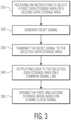
- FIG. 3illustrates an embodiment of a method for managing a plurality of storage areas in a host device.
- the methodmay be implemented, for example, by the system of FIG. 1 or by another system.
- FIG. 1it will be assumed in the following discussion that the system of FIG. 1 is used to implement the method.
- the methodincludes, at 310, receiving an instruction to select a first data storage area or a second data storage area in a host device.
- the first data storage areamay be a removable SIM card (e.g., UICC 20) and the second storage area may be embedded storage (e.g., eUICC 30).
- the embedded storage areamay be integrated on a chip with one or more other circuits, e.g., NFC circuit.
- the controller of the host devicemay receive the instruction, for example, from firmware stored in an internal memory or based on a user input (e.g., menu selection or other manual designation).
- the controllergenerates a reset signal to select the first data storage area or the second data storage area based on the instruction.
- the controllermay also be configured, based on the received instruction or another instruction, to set one or more applications (or operation of the entire host device) for use with the selected application.
- the instruction used to set operation of the host devicemay be generated by the firmware or based on a user input (e.g., menu selection).
- the controlleroutputs the reset signal to the signal line connected to the reset pin of the selected storage area.
- the controller 10may output the reset signal on line 110 if the UICC 20 is selected and may output the reset signal to line 140 if the eUICC is selected. Because different reset signal lines are used in this embodiment, the UICC and eUICC may be separately and independently selected to satisfy the data management operations of one or more intended applications.
- Additional operations of the methodmay include, at 340, outputting data to the selected storage area or receiving data from the selected storage area along an input/output signal line commonly connected to the controller of the host device, an I/O pin of the first data storage area (e.g., UICC), and an I/O pin (e.g., eUICC) of the second data storage area.
- an I/O pin of the first data storage areae.g., UICC
- an I/O pine.g., eUICC
- Another operation of the methodmay include, at 350, driving the first and second storage areas (when selected or otherwise activated) using the same clock signal.
- the same clock signalmay be output from the controller of the host device along a signal line that is commonly connected to respective clock pins of the data storage devices (e.g., UICC and eUICC). Using a single signal line for this purpose significantly reduces size, cost, and power consumption.
- a non-transitory machine-readable mediumstores instructions to cause a processor to perform the operations of the system and method embodiments described herein.
- the instructionsmay cause the processor to select a first storage area or a second storage area, generate a reset signal, and transmit the reset signal to a first signal line coupled to the first storage area or a second signal line coupled to the second storage area.
- the first storage areamay be a removable data storage card (e.g., SIM or UICC) and the second storage area is an embedded data storage area (e.g., eUICC), both of which may be located in a same host device.
- the processormay be controller 10 which performs operations as described herein.
- controller, processor, and other signal-generating and signal-processing features of the embodiments disclosed hereinmay be implemented in logic which, for example, may include hardware, software, or both.
- the controller, processor, and other signal-generating and signal-processing featuresmay be, for example, any one of a variety of integrated circuits including but not limited to an application-specific integrated circuit, a field-programmable gate array, a combination of logic gates, a system-on-chip, a microprocessor, or another type of processing or control circuit.
- the controller, processor, and other signal-generating and signal-processing featuresmay include, for example, a memory or other storage device for storing code or instructions to be executed, for example, by a computer, processor, microprocessor, controller, or other signal processing device.
- the computer, processor, microprocessor, controller, or other signal processing devicemay be those described herein or one in addition to the elements described herein. Because the algorithms that form the basis of the methods (or operations of the computer, processor, microprocessor, controller, or other signal processing device) are described in detail, the code or instructions for implementing the operations of the method embodiments may transform the computer, processor, controller, or other signal processing device into a special-purpose processor for performing the methods described herein.
Landscapes
- Engineering & Computer Science (AREA)
- Theoretical Computer Science (AREA)
- Physics & Mathematics (AREA)
- General Physics & Mathematics (AREA)
- Human Computer Interaction (AREA)
- General Engineering & Computer Science (AREA)
- Computer Networks & Wireless Communication (AREA)
- Signal Processing (AREA)
- Computer Hardware Design (AREA)
- Health & Medical Sciences (AREA)
- Toxicology (AREA)
- Microelectronics & Electronic Packaging (AREA)
- Databases & Information Systems (AREA)
- Electromagnetism (AREA)
- Computer Vision & Pattern Recognition (AREA)
- Artificial Intelligence (AREA)
- General Health & Medical Sciences (AREA)
- Telephone Function (AREA)
Description
- Example embodiments disclosed herein relate to managing data storage.
- Smartphones and other mobile devices are designed with ever increasing functionality, but not without drawbacks. For example, increasing functionality increases the numbers and sizes of chips and their supporting connections. This stands as an impediment to reducing the size of the device.
- One example of the increased functionality of smartphones is the use of near-field communications (NFC) to transmit/receive data with external devices. The data may include, for example, subscriber account and identification information, phone numbers, credit card numbers, and various types of control information. This data is stored in a subscriber identity module (SIM) card that is removably inserted into a slot of the smartphone. An example of one type of SIM card is a universal integrated circuit card (UICC).
- Use of a removable SIM card in a smartphone is not always desirable. For example, the data stored on such a card may be accessed by an unauthorized user if the smartphone is lost or stolen. One attempt to solve this problem involves using an embedded SIM storage and a removable SIM card in the same smartphone. However, this approach has been implemented in a manner that requires the use of external switches to select the embedded SIM storage or the removable SIM card. These external switches consume valuable board space and consume significant power.
US 2013/0165073 A1 describes various methods for facilitating a software smart card environment consisting of multiple virtual UICCs (vUICC) hosting a plurality of SIMS or U-SIMS. One example method may comprise receiving a network authentication request from a first network operator. The method may also comprise causing, using a processor, a UICC to activate a subscription for the first network operator and deactivate a subscription for a second network operator in an instance in which the subscription for the first network operator is not the active subscription. The method may further comprise determining a vUICC identification relating to the requested application. The method may further comprise causing authentication information to be transmitted to the first network operator based on the subscription for the first network operator.CN 102 548 046 A describes a three-card dual-standby mobile phone and a communication method thereof. The three-card dual-standby mobile phone is provided with three SIM (subscriber identity module) card holders. Furthermore, a method of realizing a three-card dual-standby function in the mobile phone is described. A one-way selective switch is additionally arranged on a data line of a second SIM card holder in a dual-card dual-standby circuit, so that a baseband processor can select a first SIM card holder and the second SIM card holder to work as a group in a dual-standby manner, or select the first SIM card holder and a third SIM card holder to work as a group in a dual-standby manner according to requirements of users.- A brief summary of various example embodiments is presented below.
- In accordance with one or more embodiments, a device is provided as defined in
claim 1. The removable data storage card may be a universal integrated circuit card (UICC), and the embedded storage area may be an embedded universal integrated circuit card (eUICC). - The device may include a circuit on a chip, wherein the eUICC is on the chip and the chip is coupled to the UICC. The circuit may be a near-field communications (NFC) circuit which reads data from or stores data to the selected one of the UICC and the eUICC. The device may include a single wire protocol (SWP) line coupled between the chip and the UICC, wherein the NFC circuit communicates with the UICC through the SWP line when the UICC is selected.
- The controller may output signals to the first signal line and the second signal line independently from one another. The controller may automatically output the signal to the first signal line or the second signal line based on an instruction stored in a memory. The controller may output the signal to the first signal line or the second signal line based on a user input signal.
- In accordance with one or more embodiments, a method for managing data storage is conceived as defined in claim 9. The removable data storage card may be a universal integrated circuit card (UICC) and the embedded storage area may be an embedded universal integrated circuit card (eUICC).
- The eUICC may be on a same chip as a circuit. The circuit may be a near-field communications (NFC) circuit which reads data from or stores data to the selected one of the UICC and the eUICC.
- Additional objects and features of the invention will be more readily apparent from the following detailed description and appended claims when taken in conjunction with the drawings. Although several example embodiments are illustrated and described, like reference numerals identify like parts in each of the figures, in which:
FIG. 1 illustrates an embodiment of a system for managing data storage in a device;FIGS. 2A and 2B illustrate examples of a user interfaces for selecting data storage devices; andFIG. 3 illustrates an embodiment of a method for managing data storage in a device.- It should be understood that the figures are merely schematic and are not drawn to scale. It should also be understood that the same reference numerals are used throughout the figures to indicate the same or similar parts.
- The descriptions and drawings illustrate the principles of various example embodiments. Furthermore, all examples recited herein are principally intended expressly to be for pedagogical purposes to aid the reader in understanding the principles of the invention and the concepts contributed by the inventor(s) to furthering the art.
- Additionally, the term, "or," as used herein, refers to a non-exclusive or (i.e., and/or), unless otherwise indicated (e.g., "or else" or "or in the alternative"). Also, the various example embodiments described herein are not necessarily mutually exclusive, as some example embodiments can be combined with one or more other example embodiments to form new example embodiments. Descriptors such as "first," "second," "third," etc., are not meant to limit the order of elements discussed, are used to distinguish one element from the next, and are generally interchangeable. Values such as maximum or minimum may be predetermined and set to different values based on the application.
FIG. 1 illustrates an embodiment of a system for managing a plurality of data storage areas in an electronic device. The data storage areas may be managed to exchange data (e.g., read, write, or both) between themselves and/or with one or more circuits or applications. The electronic device may be, for example, a mobile device such as a smartphone, tablet, personal digital assistant, media player, notebook computer, Internet of Things (IoT) device, or another type of information or processing terminal. For illustrative purposes, the electronic device may be referred to as a host device.- Referring to
FIG. 1 , the system includes acontroller 10 of the host device which manages a firstdata storage area 20 and a seconddata storage area 30. In one embodiment, the first data storage area may be a removable subscriber identity module (SIM) card and the second data storage area may be an embedded SIM storage area. In one embodiment, theSIM card 20 may be a universal integrated circuit card (UICC) and the embeddedSIM storage area 30 may be an embedded UICC (eUICC). Also, the UICC may be Class B storage and the eUICC may be 3V tolerant. - One or more of the
storage areas first storage area 20 may be referred to as a UICC and thesecond storage area 30 may be referred to as an eUICC. - The UICC 20 may include a plurality of contacts (or pins) C for sending and/or receiving power, control, and data signals. For example, the C1 contact may receive a supply voltage (SIMVCC) from the
controller 10 or a power supply of the host device. The supply voltage may activate the UICC and then provide power for performing various operations in association with the controller or other circuits of the host device. The supply voltage received throughcontact C 1 may be in different ranges to support different modes or operation, e.g., normal mode, low-power mode, etc. The contact C2 may receive a reset signal from thecontroller 10 or another circuit. The contact C3 may receive a clock signal from thecontroller 10 or another timing circuit. The contact C5 may be a connection to a reference potential, e.g., ground. The contact C6 may be a variable voltage pin to be used for programming and/or to support single wire protocol (SWP) communications, as will be discussed in greater detail below. The contact C7 may be an input/output (I/O) contact for sending and/or receiving data based on a predetermined protocol. - The
UICC 20 may include one or more other contacts (or pins) C4 and C8, which are either not used or used for an application-specific purpose. Thepin 21 for the clock signal, thepin 22 for the I/O data 22, and thepin 23 for thereset signal 23 are illustrated as inputs inFIG. 1 and are discussed below in connection with operations performed by thecontroller 10. - The
eUICC 30 may include a plurality of pins including, but not limited to, aclock input pin 31, an input/output (I/O)pin 32, and areset pin 33. TheeUICC 30 may include other pins or inputs in accordance with one or more specifications or standards, but pins 31, 32, and 33 are discussed in relation to one or more embodiments. The eUICC is embedded in the sense that is integrated into a chip including one or more other circuits. In one embodiment, theeUICC 30 may be integrated into achip 40 which includes a near-field communications (NFC)circuit 50 for communicating signals between the electronic system and an external device. The signals may include personal data, financial data, identification, and/or other data to be transmitted between theNFC circuit 50 andcontroller 10 or another circuit or application of the host device. These signals may also be transmitted between theNFC circuit 50 and an external device using an antenna coupled to a near-field communications link, for example, for purposes of making a wireless payment (e.g., using a wallet application), conveying identification information, or for another purpose. Thechip 40 may also include an embedded secure element (SE) for making secure the communications performed by theNFC circuit 50. - In one embodiment, the
eUICC 30 may store one or more applications for purposes of controlling the operations of theNFC circuit 50. In this case, theeUICC 30 may also serve as the secure element (SE). TheUICC 20 may also store applications for controlling one or more operations of the host device. TheUICC 20 and theeUICC 30, and indeed theentire chip 40, may conform to one more standards, e.g., Global System for Mobile (GSM) communications standard. TheNFC circuit 50 and theeUICC 30 are connected by internal signal lines on thechip 40. The internal signal lines may include power, data (I/O), and/or control lines to be used in sending and receiving data from theNFC circuit 50 and/or the controller of the host device. In one embodiment, theUICC 20 and theeUICC 30 may exchange data through one or more signal lines under control of thecontroller 10, for example, through signal line compatible with an ISO protocol coupled betweenUICC 20 and thechip 40 or through one or more other signal lines of the host device, e.g., I/O line(s) coupled to the host controller. The ISO protocol line may be a single wire protocol (SWP) line. In some embodiments, communication among the UICC, eUICC, and/orcontroller 10 may be performed through ISO ports. When ISO port(s) are not used, then a high impedance (HiZ) mode may be implemented so as not to disturb the active link. - The
controller 10 performs a plurality of power and management operations for theUICC 20 and theeUICC 30 and theNFC circuit 50 of the chip. Thecontroller 10 may perform these operations, for example, based on instructions (e.g., firmware) stored in amemory 60 of the host device. This memory may be any type of fixed or removable storage. - The power management operations performed by
controller 10 include providing power (e.g., SIMVCC) to one or both of theUICC 20 and thechip 40. In one embodiment, theUICC 20 may receive power from thechip 40, based on power which the chip receives from thecontroller 10. In one embodiment, a voltage source different from the controller may provide power to theUICC 20 and/or the circuits ofchip 40. - The management operations performed by the
controller 10 include selecting which of the two data storage areas is to be used for operation with the host device, and/or for performing a particular operation involving the host device. The selection is made based on signals transmitted by thecontroller 10 to respective ones of theUICC 20 andeUICC 30. - As illustrated in
FIG. 1 , the signals may be transmitted alongsignal lines Signal line 110 carries a reset signal (UIM_RST1) from thecontroller 10 to thereset input pin 23 of theUICC 20. The other signal lines may be connected to theUICC 20 and theeUICC 30. For example,signal line 120 carries a clock signal (UIM_CLK) to theinput pin 21 of theUICC 20 and to the input pin 31 (SE_ISO_CLK) of theeUICC 30. Thesignal line 130 carries data (UIM_IO) between thecontroller 10 and thepin 22 of theUICC 20 and thecontroller 10 and the pin (SE_ISO_IO) 32 of theeUICC 30. As indicated by the bidirectional arrows, thesignal line 130 may be a bidirectional line for reading data from the UICC and the eUICC and for writing (or storing) data to the UICC and the eUICC. - Thus, in the embodiment of
FIG. 1 , the clock and I/O signal lines are merged so that only one clock signal line and only one I/O line is used among all three of thecontrollers 10, theUICC 20, and theeUICC 30. By using only one signal line for the clock signal and only one signal line to perform I/O data transfers, the number of signal lines in the host device may be substantially reduced, which leads to a simpler, more space-efficient design and significant power and cost savings. - Also, in the embodiment of
FIG. 1 , a firstreset signal line 110 is used for theUICC 20 and a second,separate signal line 140 is used for theeUICC 30. The controller may use these separate reset signal lines to independently select the UICC and eUICC to perform one or more operations or applications, as determined, for example, by the firmware stored inmemory 60. In order to select theUICC 20 or eUICC 30 (for use with theNFC circuit 50 or another application of the host device), thecontroller 10 outputs a reset signal to the reset pin of the one to be selected. When thecontroller 10 outputs a reset signal to signalline 110, theUICC 20 is selected. When thecontroller 10 outputs a reset signal to signalline 140, theeUICC 30 is selected. The firmware stored inmemory 60 may instruct thecontroller 10 to use the selected one of theUICC 20 or the eUICC to which the reset signal was sent, either for all operations of the host device to the exclusion of the unselected storage or for specific operations as determined, for example, by the firmware or a user input or preference. When a reset signal is received by the UICC or the eUICC, an initialization procedure may be implemented, which may involve erasing all data previously stored therein. As a result, the full capacity of the selected data storage may be available for use for subsequent operations of the host device, the NFC circuit, and/or other applications or circuits. - The
controller 10 may output a reset signal to signalline 110 orsignal line 140 based on one or more scenarios. In one embodiment, the controller may automatically output a reset signal to select one ofUICC 20 oreUICC 30 based on instructions in the firmware stored inmemory 60. In one embodiment, the firmware may be written to designate the UICC or the eUICC as a default storage area for use with theNFC circuit 50 and/or one or more other applications or circuits upon initial start-up of the host device, when the host device is re-configured or reset, and/or based on one or more other conditions. - Another example may follow a recent trend among smartphone manufacturers who have a preference for using an embedded SIM over a removable SIM card. In the event that the host device has both
UICC 20 andeUICC 30, the controller may automatically output a reset signal to theeUICC 30, e.g., when initiated or at start-up. At any time thereafter, for example, based on instructions in the firmware or an application, the UICC may be selected when thecontroller 10 outputs a reset signal alongline 110. - In another example, the
controller 10 may output a reset signal to select one of the UICC or the eUICC based on an input signal. The user input signal may be generated, for example, by a user accessing an option in a control menu of the host device. The control menu may be included, for example, in the settings of the host device in order to allow the user to select which storage area (UICC or eUICC) is to be used to store contacts, personal identification information, financial information, and/or other information during use of the host device. For example, while use of the eUICC may be preferred by a smartphone manufacturer, the user of the host device may prefer using the UICC because of its ability to be removed from a slot in the host device for purposes of initializing a new user or host device or otherwise for protecting unauthorized access to sensitive information. FIG. 2A illustrates an example of user interface that may be displayed on the host device to allow a user to manually select use ofremovable UICC card 20 or embeddedeUICC 30. Thecontroller 10 of the host device may then output a reset signal on the appropriate one ofsignal lines FIG. 2B illustrates an example of an interface that may be displayed to allow the user to select which applications are to be used with the UICC and which applications are to be used with the eUICC. In one embodiment, a user interface may allow the user to select one of the UICC or eUICC as default storage. In one embodiment, the firmware may be written to automatically select the UICC for some applications and the eUICC for other applications, by outputting a reset signal along a corresponding one of thesignal lines - In one embodiment, the
eUICC 30 may perform a data input/output operation based on voltage from a power supply VDDIO_SE output from thecontroller 10. Thecontroller 10 may also output different levels of voltage (see the branch paths inFIG. 1 ) from a power supply VDDIO to support data input/output operations performed by theNFC circuit 50, either relative to theUICC 20 or theeUICC 30. Thecontroller 10 and thechip 40 may communicate data, control signals, and/or other information over a bus (e.g., Inter-Integrated Circuit (I2C) bus). - In one embodiment, the
UICC 20 and theeUICC 30 may perform concurrent operations (e.g., may be simultaneously enabled) under control of the controller and/or theNFC circuit 50. The concurrent operations may be related to a same operation of the host device or may be performed independently from one another, e.g., may corresponds to different and unrelated operations, circuits, or applications being performed on the host device. FIG. 3 illustrates an embodiment of a method for managing a plurality of storage areas in a host device. The method may be implemented, for example, by the system ofFIG. 1 or by another system. For illustrative purposes, it will be assumed in the following discussion that the system ofFIG. 1 is used to implement the method.- Referring to
FIG. 3 , the method includes, at 310, receiving an instruction to select a first data storage area or a second data storage area in a host device. The first data storage area may be a removable SIM card (e.g., UICC 20) and the second storage area may be embedded storage (e.g., eUICC 30). As previously indicated, the embedded storage area may be integrated on a chip with one or more other circuits, e.g., NFC circuit. The controller of the host device may receive the instruction, for example, from firmware stored in an internal memory or based on a user input (e.g., menu selection or other manual designation). - At 320, the controller generates a reset signal to select the first data storage area or the second data storage area based on the instruction. At this time, the controller may also be configured, based on the received instruction or another instruction, to set one or more applications (or operation of the entire host device) for use with the selected application. The instruction used to set operation of the host device may be generated by the firmware or based on a user input (e.g., menu selection).
- At 330, the controller outputs the reset signal to the signal line connected to the reset pin of the selected storage area. For example, in the system of
FIG. 1 , thecontroller 10 may output the reset signal online 110 if theUICC 20 is selected and may output the reset signal toline 140 if the eUICC is selected. Because different reset signal lines are used in this embodiment, the UICC and eUICC may be separately and independently selected to satisfy the data management operations of one or more intended applications. - Additional operations of the method may include, at 340, outputting data to the selected storage area or receiving data from the selected storage area along an input/output signal line commonly connected to the controller of the host device, an I/O pin of the first data storage area (e.g., UICC), and an I/O pin (e.g., eUICC) of the second data storage area. Using a single signal line for this purpose may significantly reduce size, cost, and power consumption.
- Another operation of the method may include, at 350, driving the first and second storage areas (when selected or otherwise activated) using the same clock signal. The same clock signal may be output from the controller of the host device along a signal line that is commonly connected to respective clock pins of the data storage devices (e.g., UICC and eUICC). Using a single signal line for this purpose significantly reduces size, cost, and power consumption.
- In accordance with one embodiment, a non-transitory machine-readable medium stores instructions to cause a processor to perform the operations of the system and method embodiments described herein. For example, the instructions may cause the processor to select a first storage area or a second storage area, generate a reset signal, and transmit the reset signal to a first signal line coupled to the first storage area or a second signal line coupled to the second storage area. The first storage area may be a removable data storage card (e.g., SIM or UICC) and the second storage area is an embedded data storage area (e.g., eUICC), both of which may be located in a same host device. The processor may be
controller 10 which performs operations as described herein. - The controller, processor, and other signal-generating and signal-processing features of the embodiments disclosed herein may be implemented in logic which, for example, may include hardware, software, or both. When implemented at least partially in hardware, the controller, processor, and other signal-generating and signal-processing features may be, for example, any one of a variety of integrated circuits including but not limited to an application-specific integrated circuit, a field-programmable gate array, a combination of logic gates, a system-on-chip, a microprocessor, or another type of processing or control circuit.
- When implemented in at least partially in software, the controller, processor, and other signal-generating and signal-processing features may include, for example, a memory or other storage device for storing code or instructions to be executed, for example, by a computer, processor, microprocessor, controller, or other signal processing device. The computer, processor, microprocessor, controller, or other signal processing device may be those described herein or one in addition to the elements described herein. Because the algorithms that form the basis of the methods (or operations of the computer, processor, microprocessor, controller, or other signal processing device) are described in detail, the code or instructions for implementing the operations of the method embodiments may transform the computer, processor, controller, or other signal processing device into a special-purpose processor for performing the methods described herein.
- The benefits, advantages, solutions to problems, and any element(s) that may cause any benefit, advantage, or solution to occur or become more pronounced are not to be construed as a critical, required, or essential features or elements of any or all the claims.
Claims (12)
- A device, comprising:- a first signal line (110) coupled to a first storage area (20);- a second signal line (140) coupled to a second storage area (30); and- a controller (10) configured to output a signal to the first signal line (110) or the second signal line (140) to select the first storage area (20) or the second storage area (30), wherein the first storage area (20) is a removable data storage card and the second storage area (30) is an embedded storage area in the device and wherein the signal is a reset signal for the selected one of the first storage area (20) and the second storage area (30);characterized in that the device further comprises:- a third signal line (120) being commonly connected from the controller (10) to respective clock pins of the first storage area (20) and the second storage area (30); and- a further signal line (130) being commonly connected from the controller (10) to the first storage area (20) and the second storage area (30), wherein the further signal line is a bidirectional input/output line to carry data;wherein the controller (10) is further configured to drive the selected one of the first storage area (20) and the second storage area (30) by transmitting a clock signal along the third signal line, and to output data to or receive data from the selected one of the first storage area (20) and the second storage area (30) along the further signal line.
- The device of claim 1, wherein:- the removable data storage card is a universal integrated circuit card, UICC, and- the embedded storage area is an embedded universal integrated circuit card, eUICC.
- The device of claim 2, further comprising:- a circuit on a chip (40),- wherein the eUICC is on the chip (40) and the chip (40) is coupled to the UICC.
- The device of claim 3, wherein the circuit is a near-field communications, NFC, circuit (50) which reads data from or stores data to the selected one of the UICC and the eUICC.
- The device of claim 4, further comprising:- a single wire protocol, SWP, line coupled between the chip (40) and the UICC,wherein the NFC circuit (50) communicates with the UICC through the SWP line when the UICC is selected.
- The device of any preceding claim, wherein the controller (10) is configured to output signals to the first signal line (110) and the second signal line (140) independently from one another.
- The device of any preceding claim, wherein the controller (10) is configured to automatically output the signal to the first signal line (110) or the second signal line (140) based on an instruction stored in a memory (60).
- The device of any preceding claim, wherein the controller (10) is configured to output the signal to the first signal line (110) or the second signal line (140) based on a user input signal.
- A method for managing data storage, comprising:- receiving an instruction to select a first storage area (20) or a second storage area (30);- generating, by controller (10), a reset signal; and- transmitting, by said controller (10), the reset signal to a first signal line (110) coupled to the first storage area (20) or a second signal line (140) coupled to the second storage area (30), wherein the first storage area (20) is a removable data storage card and the second storage area (30) is an embedded data storage area and wherein the removable data storage card and the embedded data storage are located in a same device;characterized in that the method further comprises:- driving, by the controller (10), the selected one of the first storage area (20) and the second storage area (30) by transmitting a clock signal along a third signal line (120) being commonly connected from the controller (10) to respective clock pins of the first storage area (20) and the second storage area (30); and- outputting data to or receiving data, by said controller (10), from the selected one of the first storage area (20) and the second storage area (30) along a further signal line (130) being commonly connected from the controller (10) to the first storage area (20) and the second storage area (30), wherein the further signal line (130) is a bidirectional input/output line.
- The method of claim 9, wherein:- the removable data storage card is a universal integrated circuit card, UICC, and- the embedded storage area is an embedded universal integrated circuit card, eUICC.
- The method of claim 10, wherein the eUICC is on a same chip (40) as a circuit.
- The method of claim 11, wherein the circuit is a near-field communications, NFC circuit (50) which reads data from or stores data to the selected one of the UICC and the eUICC.
Priority Applications (3)
| Application Number | Priority Date | Filing Date | Title |
|---|---|---|---|
| EP19305599.3AEP3737128B1 (en) | 2019-05-10 | 2019-05-10 | Common data and clock signal lines |
| US16/516,900US10872663B2 (en) | 2019-05-10 | 2019-07-19 | Data storage management in a device including removable and embedded storage areas |
| CN202010370107.0ACN111918277B (en) | 2019-05-10 | 2020-04-30 | Data storage management |
Applications Claiming Priority (1)
| Application Number | Priority Date | Filing Date | Title |
|---|---|---|---|
| EP19305599.3AEP3737128B1 (en) | 2019-05-10 | 2019-05-10 | Common data and clock signal lines |
Publications (2)
| Publication Number | Publication Date |
|---|---|
| EP3737128A1 EP3737128A1 (en) | 2020-11-11 |
| EP3737128B1true EP3737128B1 (en) | 2024-04-17 |
Family
ID=66776278
Family Applications (1)
| Application Number | Title | Priority Date | Filing Date |
|---|---|---|---|
| EP19305599.3AActiveEP3737128B1 (en) | 2019-05-10 | 2019-05-10 | Common data and clock signal lines |
Country Status (3)
| Country | Link |
|---|---|
| US (1) | US10872663B2 (en) |
| EP (1) | EP3737128B1 (en) |
| CN (1) | CN111918277B (en) |
Citations (2)
| Publication number | Priority date | Publication date | Assignee | Title |
|---|---|---|---|---|
| CN102548046A (en)* | 2010-12-24 | 2012-07-04 | 深圳市经纬科技有限公司 | Three-card dual-standby mobile phone and method of realizing three-card dual-standby function in same |
| US9531831B1 (en)* | 2016-04-05 | 2016-12-27 | Verizon Patent And Licensing Inc. | Active subscription profiles on secure element supporting concurrent usage of network services |
Family Cites Families (17)
| Publication number | Priority date | Publication date | Assignee | Title |
|---|---|---|---|---|
| US20100125689A1 (en)* | 2008-11-20 | 2010-05-20 | Mediatek Inc. | Electronic apparatus capable of receiving different types of memory cards |
| EP2461613A1 (en)* | 2010-12-06 | 2012-06-06 | Gemalto SA | Methods and system for handling UICC data |
| IT1404159B1 (en)* | 2010-12-30 | 2013-11-15 | Incard Sa | METHOD AND SYSTEM OF CONTROL OF A COMMUNICATION BETWEEN AN INTEGRATED CIRCUIT UNIVERSAL CARD AND AN EXTERNAL APPLICATION |
| US8560015B2 (en)* | 2011-07-18 | 2013-10-15 | Nokia Corporation | Application selection for multi-SIM environment |
| WO2013027085A1 (en)* | 2011-08-22 | 2013-02-28 | Nokia Corporation | Multi-sim enabling application and use of euicc in legacy terminals |
| US8954067B2 (en)* | 2011-12-23 | 2015-02-10 | Nokia Corporation | Method and apparatus for emulating a plurality of subscriptions |
| EP3116161B1 (en)* | 2014-04-01 | 2018-03-14 | Huawei Device (Dongguan) Co., Ltd. | Security unit management method and terminal |
| KR102331692B1 (en)* | 2014-06-30 | 2021-11-30 | 삼성전자 주식회사 | Method and apparatus for selecting profile of terminal in a mobile network |
| KR102219451B1 (en)* | 2014-09-22 | 2021-02-24 | 삼성전자주식회사 | Storage controller, method of operating the same and solid state disk including the same |
| US10084698B2 (en)* | 2015-03-26 | 2018-09-25 | Intel Corporation | Selectively enabling first and second communication paths using a repeater |
| CN106611608B (en)* | 2015-10-23 | 2019-01-15 | 群联电子股份有限公司 | Memory control circuit unit, memory storage device and data transmission method |
| KR102349553B1 (en)* | 2015-10-29 | 2022-01-12 | 삼성전자주식회사 | Communication circuit chip and electronic device configured to communicate with plural memory cards |
| FR3043229B1 (en)* | 2015-11-03 | 2018-03-30 | Proton World International N.V. | SECURE STARTING OF AN ELECTRONIC CIRCUIT |
| KR102484367B1 (en)* | 2016-09-09 | 2023-01-04 | 삼성전자주식회사 | Method and System for Controlling UICC and eUICC |
| EP3376458B1 (en)* | 2017-03-15 | 2020-07-15 | Nxp B.V. | Nfc device and initialization method |
| EP3413600B1 (en)* | 2017-06-08 | 2020-02-19 | Nxp B.V. | Communication device and method of managing profiles |
| US10779157B2 (en)* | 2017-09-28 | 2020-09-15 | Apple Inc. | Methods and apparatus for accessing services of multiple wireless networks via a single radio access network |
- 2019
- 2019-05-10EPEP19305599.3Apatent/EP3737128B1/enactiveActive
- 2019-07-19USUS16/516,900patent/US10872663B2/enactiveActive
- 2020
- 2020-04-30CNCN202010370107.0Apatent/CN111918277B/enactiveActive
Patent Citations (2)
| Publication number | Priority date | Publication date | Assignee | Title |
|---|---|---|---|---|
| CN102548046A (en)* | 2010-12-24 | 2012-07-04 | 深圳市经纬科技有限公司 | Three-card dual-standby mobile phone and method of realizing three-card dual-standby function in same |
| US9531831B1 (en)* | 2016-04-05 | 2016-12-27 | Verizon Patent And Licensing Inc. | Active subscription profiles on secure element supporting concurrent usage of network services |
Also Published As
| Publication number | Publication date |
|---|---|
| CN111918277B (en) | 2024-05-28 |
| US20200357465A1 (en) | 2020-11-12 |
| CN111918277A (en) | 2020-11-10 |
| US10872663B2 (en) | 2020-12-22 |
| EP3737128A1 (en) | 2020-11-11 |
Similar Documents
| Publication | Publication Date | Title |
|---|---|---|
| US9420409B2 (en) | Near field communication device | |
| US7865141B2 (en) | Chipset for mobile wallet system | |
| US9741027B2 (en) | Memory card based contactless devices | |
| US9673870B2 (en) | Near-field communications and routing | |
| JP2007242024A (en) | IC card, portable terminal and control method of portable terminal | |
| SG173004A1 (en) | Portable mobile communication device and method of controlling near field communication | |
| CN104239829A (en) | Near-field communication device and method thereof | |
| CN114401508A (en) | SIM card management method and electronic device | |
| US7986962B2 (en) | Providing a high-speed connection between a memory medium of a mobile device and an external device | |
| EP3737128B1 (en) | Common data and clock signal lines | |
| US10552826B2 (en) | Selecting an application on a card | |
| CN111598206A (en) | Multifunctional SIM card and terminal equipment | |
| US9237157B2 (en) | Data processing and storage device | |
| JP5636008B2 (en) | Mobile terminal, program, recording medium | |
| EP3236393B1 (en) | Control of an external interface on a card | |
| KR100455990B1 (en) | Mobile wireless device with user identify card sharing memory card | |
| CN101754448A (en) | Dual-core intelligent card for mobile communication and data transmission and processing method thereof | |
| US9277409B2 (en) | Security chip of a communication device | |
| WO2012079429A1 (en) | Storage device and configuration method thereof | |
| CN109831762B (en) | POS data communication method, device, terminal equipment and system | |
| KR20060047052A (en) | Initialization method of multi interface card and multi interface card | |
| EP3086272A1 (en) | Selecting an application on a card |
Legal Events
| Date | Code | Title | Description |
|---|---|---|---|
| PUAI | Public reference made under article 153(3) epc to a published international application that has entered the european phase | Free format text:ORIGINAL CODE: 0009012 | |
| STAA | Information on the status of an ep patent application or granted ep patent | Free format text:STATUS: THE APPLICATION HAS BEEN PUBLISHED | |
| AK | Designated contracting states | Kind code of ref document:A1 Designated state(s):AL AT BE BG CH CY CZ DE DK EE ES FI FR GB GR HR HU IE IS IT LI LT LU LV MC MK MT NL NO PL PT RO RS SE SI SK SM TR | |
| AX | Request for extension of the european patent | Extension state:BA ME | |
| STAA | Information on the status of an ep patent application or granted ep patent | Free format text:STATUS: REQUEST FOR EXAMINATION WAS MADE | |
| 17P | Request for examination filed | Effective date:20210511 | |
| RBV | Designated contracting states (corrected) | Designated state(s):AL AT BE BG CH CY CZ DE DK EE ES FI FR GB GR HR HU IE IS IT LI LT LU LV MC MK MT NL NO PL PT RO RS SE SI SK SM TR | |
| STAA | Information on the status of an ep patent application or granted ep patent | Free format text:STATUS: EXAMINATION IS IN PROGRESS | |
| 17Q | First examination report despatched | Effective date:20221004 | |
| GRAP | Despatch of communication of intention to grant a patent | Free format text:ORIGINAL CODE: EPIDOSNIGR1 | |
| STAA | Information on the status of an ep patent application or granted ep patent | Free format text:STATUS: GRANT OF PATENT IS INTENDED | |
| RIC1 | Information provided on ipc code assigned before grant | Ipc:H04W 88/06 20090101ALN20231221BHEP Ipc:H04W 8/18 20090101AFI20231221BHEP | |
| INTG | Intention to grant announced | Effective date:20240112 | |
| GRAS | Grant fee paid | Free format text:ORIGINAL CODE: EPIDOSNIGR3 | |
| GRAA | (expected) grant | Free format text:ORIGINAL CODE: 0009210 | |
| STAA | Information on the status of an ep patent application or granted ep patent | Free format text:STATUS: THE PATENT HAS BEEN GRANTED | |
| AK | Designated contracting states | Kind code of ref document:B1 Designated state(s):AL AT BE BG CH CY CZ DE DK EE ES FI FR GB GR HR HU IE IS IT LI LT LU LV MC MK MT NL NO PL PT RO RS SE SI SK SM TR | |
| REG | Reference to a national code | Ref country code:GB Ref legal event code:FG4D | |
| REG | Reference to a national code | Ref country code:CH Ref legal event code:EP | |
| REG | Reference to a national code | Ref country code:IE Ref legal event code:FG4D Ref country code:DE Ref legal event code:R096 Ref document number:602019050379 Country of ref document:DE | |
| REG | Reference to a national code | Ref country code:LT Ref legal event code:MG9D | |
| REG | Reference to a national code | Ref country code:NL Ref legal event code:MP Effective date:20240417 | |
| REG | Reference to a national code | Ref country code:AT Ref legal event code:MK05 Ref document number:1678418 Country of ref document:AT Kind code of ref document:T Effective date:20240417 | |
| PG25 | Lapsed in a contracting state [announced via postgrant information from national office to epo] | Ref country code:NL Free format text:LAPSE BECAUSE OF FAILURE TO SUBMIT A TRANSLATION OF THE DESCRIPTION OR TO PAY THE FEE WITHIN THE PRESCRIBED TIME-LIMIT Effective date:20240417 | |
| PG25 | Lapsed in a contracting state [announced via postgrant information from national office to epo] | Ref country code:NL Free format text:LAPSE BECAUSE OF FAILURE TO SUBMIT A TRANSLATION OF THE DESCRIPTION OR TO PAY THE FEE WITHIN THE PRESCRIBED TIME-LIMIT Effective date:20240417 | |
| PG25 | Lapsed in a contracting state [announced via postgrant information from national office to epo] | Ref country code:IS Free format text:LAPSE BECAUSE OF FAILURE TO SUBMIT A TRANSLATION OF THE DESCRIPTION OR TO PAY THE FEE WITHIN THE PRESCRIBED TIME-LIMIT Effective date:20240817 | |
| PG25 | Lapsed in a contracting state [announced via postgrant information from national office to epo] | Ref country code:BG Free format text:LAPSE BECAUSE OF FAILURE TO SUBMIT A TRANSLATION OF THE DESCRIPTION OR TO PAY THE FEE WITHIN THE PRESCRIBED TIME-LIMIT Effective date:20240417 | |
| PG25 | Lapsed in a contracting state [announced via postgrant information from national office to epo] | Ref country code:HR Free format text:LAPSE BECAUSE OF FAILURE TO SUBMIT A TRANSLATION OF THE DESCRIPTION OR TO PAY THE FEE WITHIN THE PRESCRIBED TIME-LIMIT Effective date:20240417 Ref country code:FI Free format text:LAPSE BECAUSE OF FAILURE TO SUBMIT A TRANSLATION OF THE DESCRIPTION OR TO PAY THE FEE WITHIN THE PRESCRIBED TIME-LIMIT Effective date:20240417 | |
| PG25 | Lapsed in a contracting state [announced via postgrant information from national office to epo] | Ref country code:GR Free format text:LAPSE BECAUSE OF FAILURE TO SUBMIT A TRANSLATION OF THE DESCRIPTION OR TO PAY THE FEE WITHIN THE PRESCRIBED TIME-LIMIT Effective date:20240718 | |
| PG25 | Lapsed in a contracting state [announced via postgrant information from national office to epo] | Ref country code:PT Free format text:LAPSE BECAUSE OF FAILURE TO SUBMIT A TRANSLATION OF THE DESCRIPTION OR TO PAY THE FEE WITHIN THE PRESCRIBED TIME-LIMIT Effective date:20240819 | |
| PG25 | Lapsed in a contracting state [announced via postgrant information from national office to epo] | Ref country code:ES Free format text:LAPSE BECAUSE OF FAILURE TO SUBMIT A TRANSLATION OF THE DESCRIPTION OR TO PAY THE FEE WITHIN THE PRESCRIBED TIME-LIMIT Effective date:20240417 | |
| PG25 | Lapsed in a contracting state [announced via postgrant information from national office to epo] | Ref country code:AT Free format text:LAPSE BECAUSE OF FAILURE TO SUBMIT A TRANSLATION OF THE DESCRIPTION OR TO PAY THE FEE WITHIN THE PRESCRIBED TIME-LIMIT Effective date:20240417 | |
| PG25 | Lapsed in a contracting state [announced via postgrant information from national office to epo] | Ref country code:PL Free format text:LAPSE BECAUSE OF FAILURE TO SUBMIT A TRANSLATION OF THE DESCRIPTION OR TO PAY THE FEE WITHIN THE PRESCRIBED TIME-LIMIT Effective date:20240417 | |
| PG25 | Lapsed in a contracting state [announced via postgrant information from national office to epo] | Ref country code:LV Free format text:LAPSE BECAUSE OF FAILURE TO SUBMIT A TRANSLATION OF THE DESCRIPTION OR TO PAY THE FEE WITHIN THE PRESCRIBED TIME-LIMIT Effective date:20240417 | |
| PG25 | Lapsed in a contracting state [announced via postgrant information from national office to epo] | Ref country code:PT Free format text:LAPSE BECAUSE OF FAILURE TO SUBMIT A TRANSLATION OF THE DESCRIPTION OR TO PAY THE FEE WITHIN THE PRESCRIBED TIME-LIMIT Effective date:20240819 Ref country code:PL Free format text:LAPSE BECAUSE OF FAILURE TO SUBMIT A TRANSLATION OF THE DESCRIPTION OR TO PAY THE FEE WITHIN THE PRESCRIBED TIME-LIMIT Effective date:20240417 Ref country code:NO Free format text:LAPSE BECAUSE OF FAILURE TO SUBMIT A TRANSLATION OF THE DESCRIPTION OR TO PAY THE FEE WITHIN THE PRESCRIBED TIME-LIMIT Effective date:20240717 Ref country code:LV Free format text:LAPSE BECAUSE OF FAILURE TO SUBMIT A TRANSLATION OF THE DESCRIPTION OR TO PAY THE FEE WITHIN THE PRESCRIBED TIME-LIMIT Effective date:20240417 Ref country code:IS Free format text:LAPSE BECAUSE OF FAILURE TO SUBMIT A TRANSLATION OF THE DESCRIPTION OR TO PAY THE FEE WITHIN THE PRESCRIBED TIME-LIMIT Effective date:20240817 Ref country code:HR Free format text:LAPSE BECAUSE OF FAILURE TO SUBMIT A TRANSLATION OF THE DESCRIPTION OR TO PAY THE FEE WITHIN THE PRESCRIBED TIME-LIMIT Effective date:20240417 Ref country code:GR Free format text:LAPSE BECAUSE OF FAILURE TO SUBMIT A TRANSLATION OF THE DESCRIPTION OR TO PAY THE FEE WITHIN THE PRESCRIBED TIME-LIMIT Effective date:20240718 Ref country code:FI Free format text:LAPSE BECAUSE OF FAILURE TO SUBMIT A TRANSLATION OF THE DESCRIPTION OR TO PAY THE FEE WITHIN THE PRESCRIBED TIME-LIMIT Effective date:20240417 Ref country code:ES Free format text:LAPSE BECAUSE OF FAILURE TO SUBMIT A TRANSLATION OF THE DESCRIPTION OR TO PAY THE FEE WITHIN THE PRESCRIBED TIME-LIMIT Effective date:20240417 Ref country code:BG Free format text:LAPSE BECAUSE OF FAILURE TO SUBMIT A TRANSLATION OF THE DESCRIPTION OR TO PAY THE FEE WITHIN THE PRESCRIBED TIME-LIMIT Effective date:20240417 Ref country code:AT Free format text:LAPSE BECAUSE OF FAILURE TO SUBMIT A TRANSLATION OF THE DESCRIPTION OR TO PAY THE FEE WITHIN THE PRESCRIBED TIME-LIMIT Effective date:20240417 Ref country code:RS Free format text:LAPSE BECAUSE OF FAILURE TO SUBMIT A TRANSLATION OF THE DESCRIPTION OR TO PAY THE FEE WITHIN THE PRESCRIBED TIME-LIMIT Effective date:20240717 | |
| REG | Reference to a national code | Ref country code:CH Ref legal event code:PL | |
| PG25 | Lapsed in a contracting state [announced via postgrant information from national office to epo] | Ref country code:DK Free format text:LAPSE BECAUSE OF FAILURE TO SUBMIT A TRANSLATION OF THE DESCRIPTION OR TO PAY THE FEE WITHIN THE PRESCRIBED TIME-LIMIT Effective date:20240417 | |
| PG25 | Lapsed in a contracting state [announced via postgrant information from national office to epo] | Ref country code:LU Free format text:LAPSE BECAUSE OF NON-PAYMENT OF DUE FEES Effective date:20240510 | |
| REG | Reference to a national code | Ref country code:DE Ref legal event code:R097 Ref document number:602019050379 Country of ref document:DE | |
| PG25 | Lapsed in a contracting state [announced via postgrant information from national office to epo] | Ref country code:EE Free format text:LAPSE BECAUSE OF FAILURE TO SUBMIT A TRANSLATION OF THE DESCRIPTION OR TO PAY THE FEE WITHIN THE PRESCRIBED TIME-LIMIT Effective date:20240417 | |
| PG25 | Lapsed in a contracting state [announced via postgrant information from national office to epo] | Ref country code:CZ Free format text:LAPSE BECAUSE OF FAILURE TO SUBMIT A TRANSLATION OF THE DESCRIPTION OR TO PAY THE FEE WITHIN THE PRESCRIBED TIME-LIMIT Effective date:20240417 | |
| PG25 | Lapsed in a contracting state [announced via postgrant information from national office to epo] | Ref country code:SK Free format text:LAPSE BECAUSE OF FAILURE TO SUBMIT A TRANSLATION OF THE DESCRIPTION OR TO PAY THE FEE WITHIN THE PRESCRIBED TIME-LIMIT Effective date:20240417 Ref country code:RO Free format text:LAPSE BECAUSE OF FAILURE TO SUBMIT A TRANSLATION OF THE DESCRIPTION OR TO PAY THE FEE WITHIN THE PRESCRIBED TIME-LIMIT Effective date:20240417 | |
| PG25 | Lapsed in a contracting state [announced via postgrant information from national office to epo] | Ref country code:SM Free format text:LAPSE BECAUSE OF FAILURE TO SUBMIT A TRANSLATION OF THE DESCRIPTION OR TO PAY THE FEE WITHIN THE PRESCRIBED TIME-LIMIT Effective date:20240417 | |
| PG25 | Lapsed in a contracting state [announced via postgrant information from national office to epo] | Ref country code:SM Free format text:LAPSE BECAUSE OF FAILURE TO SUBMIT A TRANSLATION OF THE DESCRIPTION OR TO PAY THE FEE WITHIN THE PRESCRIBED TIME-LIMIT Effective date:20240417 Ref country code:SK Free format text:LAPSE BECAUSE OF FAILURE TO SUBMIT A TRANSLATION OF THE DESCRIPTION OR TO PAY THE FEE WITHIN THE PRESCRIBED TIME-LIMIT Effective date:20240417 Ref country code:RO Free format text:LAPSE BECAUSE OF FAILURE TO SUBMIT A TRANSLATION OF THE DESCRIPTION OR TO PAY THE FEE WITHIN THE PRESCRIBED TIME-LIMIT Effective date:20240417 Ref country code:LU Free format text:LAPSE BECAUSE OF NON-PAYMENT OF DUE FEES Effective date:20240510 Ref country code:EE Free format text:LAPSE BECAUSE OF FAILURE TO SUBMIT A TRANSLATION OF THE DESCRIPTION OR TO PAY THE FEE WITHIN THE PRESCRIBED TIME-LIMIT Effective date:20240417 Ref country code:DK Free format text:LAPSE BECAUSE OF FAILURE TO SUBMIT A TRANSLATION OF THE DESCRIPTION OR TO PAY THE FEE WITHIN THE PRESCRIBED TIME-LIMIT Effective date:20240417 Ref country code:CZ Free format text:LAPSE BECAUSE OF FAILURE TO SUBMIT A TRANSLATION OF THE DESCRIPTION OR TO PAY THE FEE WITHIN THE PRESCRIBED TIME-LIMIT Effective date:20240417 Ref country code:CH Free format text:LAPSE BECAUSE OF NON-PAYMENT OF DUE FEES Effective date:20240531 Ref country code:MC Free format text:LAPSE BECAUSE OF FAILURE TO SUBMIT A TRANSLATION OF THE DESCRIPTION OR TO PAY THE FEE WITHIN THE PRESCRIBED TIME-LIMIT Effective date:20240417 | |
| PG25 | Lapsed in a contracting state [announced via postgrant information from national office to epo] | Ref country code:IT Free format text:LAPSE BECAUSE OF FAILURE TO SUBMIT A TRANSLATION OF THE DESCRIPTION OR TO PAY THE FEE WITHIN THE PRESCRIBED TIME-LIMIT Effective date:20240417 | |
| PLBE | No opposition filed within time limit | Free format text:ORIGINAL CODE: 0009261 | |
| REG | Reference to a national code | Ref country code:BE Ref legal event code:MM Effective date:20240531 | |
| STAA | Information on the status of an ep patent application or granted ep patent | Free format text:STATUS: NO OPPOSITION FILED WITHIN TIME LIMIT | |
| 26N | No opposition filed | Effective date:20250120 | |
| GBPC | Gb: european patent ceased through non-payment of renewal fee | Effective date:20240717 | |
| PG25 | Lapsed in a contracting state [announced via postgrant information from national office to epo] | Ref country code:IE Free format text:LAPSE BECAUSE OF NON-PAYMENT OF DUE FEES Effective date:20240510 | |
| PG25 | Lapsed in a contracting state [announced via postgrant information from national office to epo] | Ref country code:SI Free format text:LAPSE BECAUSE OF FAILURE TO SUBMIT A TRANSLATION OF THE DESCRIPTION OR TO PAY THE FEE WITHIN THE PRESCRIBED TIME-LIMIT Effective date:20240417 Ref country code:BE Free format text:LAPSE BECAUSE OF NON-PAYMENT OF DUE FEES Effective date:20240531 | |
| PG25 | Lapsed in a contracting state [announced via postgrant information from national office to epo] | Ref country code:GB Free format text:LAPSE BECAUSE OF NON-PAYMENT OF DUE FEES Effective date:20240717 | |
| PGFP | Annual fee paid to national office [announced via postgrant information from national office to epo] | Ref country code:DE Payment date:20250423 Year of fee payment:7 | |
| PGFP | Annual fee paid to national office [announced via postgrant information from national office to epo] | Ref country code:FR Payment date:20250424 Year of fee payment:7 | |
| P01 | Opt-out of the competence of the unified patent court (upc) registered | Free format text:CASE NUMBER: APP_29865/2025 Effective date:20250623 | |
| PG25 | Lapsed in a contracting state [announced via postgrant information from national office to epo] | Ref country code:CY Free format text:LAPSE BECAUSE OF FAILURE TO SUBMIT A TRANSLATION OF THE DESCRIPTION OR TO PAY THE FEE WITHIN THE PRESCRIBED TIME-LIMIT; INVALID AB INITIO Effective date:20190510 | |
| PG25 | Lapsed in a contracting state [announced via postgrant information from national office to epo] | Ref country code:HU Free format text:LAPSE BECAUSE OF FAILURE TO SUBMIT A TRANSLATION OF THE DESCRIPTION OR TO PAY THE FEE WITHIN THE PRESCRIBED TIME-LIMIT; INVALID AB INITIO Effective date:20190510 | |
| PG25 | Lapsed in a contracting state [announced via postgrant information from national office to epo] | Ref country code:SE Free format text:LAPSE BECAUSE OF FAILURE TO SUBMIT A TRANSLATION OF THE DESCRIPTION OR TO PAY THE FEE WITHIN THE PRESCRIBED TIME-LIMIT Effective date:20240417 |