EP3648253B1 - Crimp connection terminal - Google Patents
Crimp connection terminalDownload PDFInfo
- Publication number
- EP3648253B1 EP3648253B1EP19197263.7AEP19197263AEP3648253B1EP 3648253 B1EP3648253 B1EP 3648253B1EP 19197263 AEP19197263 AEP 19197263AEP 3648253 B1EP3648253 B1EP 3648253B1
- Authority
- EP
- European Patent Office
- Prior art keywords
- crimping
- conductor
- layer plate
- connection terminal
- lower layer
- Prior art date
- Legal status (The legal status is an assumption and is not a legal conclusion. Google has not performed a legal analysis and makes no representation as to the accuracy of the status listed.)
- Active
Links
- 238000002788crimpingMethods0.000claimsdescription75
- 239000004020conductorSubstances0.000claimsdescription60
- 239000011800void materialSubstances0.000claimsdescription13
- 239000002184metalSubstances0.000claimsdescription11
- 229910052751metalInorganic materials0.000claimsdescription11
- 238000000034methodMethods0.000claimsdescription9
- 238000005452bendingMethods0.000claimsdescription5
- XLYOFNOQVPJJNP-UHFFFAOYSA-NwaterSubstancesOXLYOFNOQVPJJNP-UHFFFAOYSA-N0.000claimsdescription4
- 238000004080punchingMethods0.000claimsdescription3
- 239000000835fiberSubstances0.000description12
- 238000003780insertionMethods0.000description5
- 230000037431insertionEffects0.000description5
- RYGMFSIKBFXOCR-UHFFFAOYSA-NCopperChemical compound[Cu]RYGMFSIKBFXOCR-UHFFFAOYSA-N0.000description3
- 229910052802copperInorganic materials0.000description3
- 239000010949copperSubstances0.000description3
- 230000004048modificationEffects0.000description3
- 238000012986modificationMethods0.000description3
- 238000000465mouldingMethods0.000description3
- 238000007747platingMethods0.000description3
- 229910001369BrassInorganic materials0.000description1
- ATJFFYVFTNAWJD-UHFFFAOYSA-NTinChemical compound[Sn]ATJFFYVFTNAWJD-UHFFFAOYSA-N0.000description1
- 229920006231aramid fiberPolymers0.000description1
- 239000010951brassSubstances0.000description1
- 238000010586diagramMethods0.000description1
- 230000010354integrationEffects0.000description1
- 230000007246mechanismEffects0.000description1
- 229910052763palladiumInorganic materials0.000description1
- 239000003381stabilizerSubstances0.000description1
- 230000000087stabilizing effectEffects0.000description1
Images


Classifications
- H—ELECTRICITY
- H01—ELECTRIC ELEMENTS
- H01R—ELECTRICALLY-CONDUCTIVE CONNECTIONS; STRUCTURAL ASSOCIATIONS OF A PLURALITY OF MUTUALLY-INSULATED ELECTRICAL CONNECTING ELEMENTS; COUPLING DEVICES; CURRENT COLLECTORS
- H01R4/00—Electrically-conductive connections between two or more conductive members in direct contact, i.e. touching one another; Means for effecting or maintaining such contact; Electrically-conductive connections having two or more spaced connecting locations for conductors and using contact members penetrating insulation
- H01R4/10—Electrically-conductive connections between two or more conductive members in direct contact, i.e. touching one another; Means for effecting or maintaining such contact; Electrically-conductive connections having two or more spaced connecting locations for conductors and using contact members penetrating insulation effected solely by twisting, wrapping, bending, crimping, or other permanent deformation
- H01R4/18—Electrically-conductive connections between two or more conductive members in direct contact, i.e. touching one another; Means for effecting or maintaining such contact; Electrically-conductive connections having two or more spaced connecting locations for conductors and using contact members penetrating insulation effected solely by twisting, wrapping, bending, crimping, or other permanent deformation by crimping
- H01R4/183—Electrically-conductive connections between two or more conductive members in direct contact, i.e. touching one another; Means for effecting or maintaining such contact; Electrically-conductive connections having two or more spaced connecting locations for conductors and using contact members penetrating insulation effected solely by twisting, wrapping, bending, crimping, or other permanent deformation by crimping for cylindrical elongated bodies, e.g. cables having circular cross-section
- H01R4/184—Electrically-conductive connections between two or more conductive members in direct contact, i.e. touching one another; Means for effecting or maintaining such contact; Electrically-conductive connections having two or more spaced connecting locations for conductors and using contact members penetrating insulation effected solely by twisting, wrapping, bending, crimping, or other permanent deformation by crimping for cylindrical elongated bodies, e.g. cables having circular cross-section comprising a U-shaped wire-receiving portion
- H01R4/185—Electrically-conductive connections between two or more conductive members in direct contact, i.e. touching one another; Means for effecting or maintaining such contact; Electrically-conductive connections having two or more spaced connecting locations for conductors and using contact members penetrating insulation effected solely by twisting, wrapping, bending, crimping, or other permanent deformation by crimping for cylindrical elongated bodies, e.g. cables having circular cross-section comprising a U-shaped wire-receiving portion combined with a U-shaped insulation-receiving portion
- H—ELECTRICITY
- H01—ELECTRIC ELEMENTS
- H01R—ELECTRICALLY-CONDUCTIVE CONNECTIONS; STRUCTURAL ASSOCIATIONS OF A PLURALITY OF MUTUALLY-INSULATED ELECTRICAL CONNECTING ELEMENTS; COUPLING DEVICES; CURRENT COLLECTORS
- H01R4/00—Electrically-conductive connections between two or more conductive members in direct contact, i.e. touching one another; Means for effecting or maintaining such contact; Electrically-conductive connections having two or more spaced connecting locations for conductors and using contact members penetrating insulation
- H01R4/10—Electrically-conductive connections between two or more conductive members in direct contact, i.e. touching one another; Means for effecting or maintaining such contact; Electrically-conductive connections having two or more spaced connecting locations for conductors and using contact members penetrating insulation effected solely by twisting, wrapping, bending, crimping, or other permanent deformation
- H01R4/18—Electrically-conductive connections between two or more conductive members in direct contact, i.e. touching one another; Means for effecting or maintaining such contact; Electrically-conductive connections having two or more spaced connecting locations for conductors and using contact members penetrating insulation effected solely by twisting, wrapping, bending, crimping, or other permanent deformation by crimping
- H01R4/20—Electrically-conductive connections between two or more conductive members in direct contact, i.e. touching one another; Means for effecting or maintaining such contact; Electrically-conductive connections having two or more spaced connecting locations for conductors and using contact members penetrating insulation effected solely by twisting, wrapping, bending, crimping, or other permanent deformation by crimping using a crimping sleeve
- H—ELECTRICITY
- H01—ELECTRIC ELEMENTS
- H01R—ELECTRICALLY-CONDUCTIVE CONNECTIONS; STRUCTURAL ASSOCIATIONS OF A PLURALITY OF MUTUALLY-INSULATED ELECTRICAL CONNECTING ELEMENTS; COUPLING DEVICES; CURRENT COLLECTORS
- H01R4/00—Electrically-conductive connections between two or more conductive members in direct contact, i.e. touching one another; Means for effecting or maintaining such contact; Electrically-conductive connections having two or more spaced connecting locations for conductors and using contact members penetrating insulation
- H01R4/10—Electrically-conductive connections between two or more conductive members in direct contact, i.e. touching one another; Means for effecting or maintaining such contact; Electrically-conductive connections having two or more spaced connecting locations for conductors and using contact members penetrating insulation effected solely by twisting, wrapping, bending, crimping, or other permanent deformation
- H01R4/18—Electrically-conductive connections between two or more conductive members in direct contact, i.e. touching one another; Means for effecting or maintaining such contact; Electrically-conductive connections having two or more spaced connecting locations for conductors and using contact members penetrating insulation effected solely by twisting, wrapping, bending, crimping, or other permanent deformation by crimping
- H01R4/183—Electrically-conductive connections between two or more conductive members in direct contact, i.e. touching one another; Means for effecting or maintaining such contact; Electrically-conductive connections having two or more spaced connecting locations for conductors and using contact members penetrating insulation effected solely by twisting, wrapping, bending, crimping, or other permanent deformation by crimping for cylindrical elongated bodies, e.g. cables having circular cross-section
- H01R4/184—Electrically-conductive connections between two or more conductive members in direct contact, i.e. touching one another; Means for effecting or maintaining such contact; Electrically-conductive connections having two or more spaced connecting locations for conductors and using contact members penetrating insulation effected solely by twisting, wrapping, bending, crimping, or other permanent deformation by crimping for cylindrical elongated bodies, e.g. cables having circular cross-section comprising a U-shaped wire-receiving portion
- H—ELECTRICITY
- H01—ELECTRIC ELEMENTS
- H01R—ELECTRICALLY-CONDUCTIVE CONNECTIONS; STRUCTURAL ASSOCIATIONS OF A PLURALITY OF MUTUALLY-INSULATED ELECTRICAL CONNECTING ELEMENTS; COUPLING DEVICES; CURRENT COLLECTORS
- H01R43/00—Apparatus or processes specially adapted for manufacturing, assembling, maintaining, or repairing of line connectors or current collectors or for joining electric conductors
- H01R43/04—Apparatus or processes specially adapted for manufacturing, assembling, maintaining, or repairing of line connectors or current collectors or for joining electric conductors for forming connections by deformation, e.g. crimping tool
- H01R43/048—Crimping apparatus or processes
- H—ELECTRICITY
- H01—ELECTRIC ELEMENTS
- H01R—ELECTRICALLY-CONDUCTIVE CONNECTIONS; STRUCTURAL ASSOCIATIONS OF A PLURALITY OF MUTUALLY-INSULATED ELECTRICAL CONNECTING ELEMENTS; COUPLING DEVICES; CURRENT COLLECTORS
- H01R43/00—Apparatus or processes specially adapted for manufacturing, assembling, maintaining, or repairing of line connectors or current collectors or for joining electric conductors
- H01R43/16—Apparatus or processes specially adapted for manufacturing, assembling, maintaining, or repairing of line connectors or current collectors or for joining electric conductors for manufacturing contact members, e.g. by punching and by bending
Definitions
- the present inventionrelates to a crimp connection terminal, for example, a crimp connection terminal internally mounted in a connector housing and fit with a connection terminal of a counterpart connector.
- connection terminalused for connection of a circuit.
- a rectangular insertion portionhaving a diameter smaller than that of an electric wire to be connected and an outer diameter of about 0.5 mm ⁇ 0.5 mm is used as a rod-shaped insertion portion inserted into a counterpart connection terminal.
- connection terminal used for a fiber wire having a large number of extremely thin core wiresis used for a connection terminal used for a fiber wire having a large number of extremely thin core wires.
- connection terminalIn a case in which a fiber wire is crimped to a connection terminal, since a conductor portion of the fiber wire is obtained by forming copper plating around an extremely fine fiber core wire and twisting a plurality of core wires together, the conductor portion is poor in extensibility and plasticity, and highly reliable connection to the fiber wire by the small connection terminal is fairly difficult. When the connection terminal is insufficiently fixed to the fiber wire, the fiber wire is easily pulled out of the connection terminal, and it is difficult to obtain excellent conductivity.
- JP-A-2017-162792is one conventional example for connecting the fiber wire in this way.
- US 4142771 Adiscloses a crimpable terminal device in which the barrel is double walled, with the inner wall being formed from the same sheet of metal as the outer wall.
- An object of the inventionis to solve the above-mentioned problem, and provide a crimp connection terminal capable of reliably caulking and holding a conductor portion of a fiber wire by a conductor crimping portion having a unique structure and ensuring reliability of electric connection.
- a crimp connection terminalfor achieving the object is a crimp connection terminal formed by punching and bending one conductive metal plate to caulk and fix an electric wire, wherein a connection portion connected to a connection terminal of a counterpart connecter is disposed at a front side, a conductor crimping portion to crimp and fix a conductor portion of the electric wire is disposed at a rear side, the conductor crimping portion has a pair of crimping pieces raised in a U-shape from a bottom portion, each of the crimping pieces of the conductor crimping portion has a lower layer plate and an upper layer plate formed by folding back from an upper end of the lower layer plate and stacking on the lower layer plate, wherein a void is formed at the folded-back portion between the lower layer plate and the upper layer plate, characterized in that the void (3g) has a cross section corresponding to a water droplet shape, a balloon shape, a circular shape, or an elliptical
- the crimp connection terminalit is possible to reliably crimp and connect a conductor portion of a fiber wire in which a plurality of core wires is twisted together to a conductor by a conductor crimping portion and to obtain excellent fixing force and conductivity.
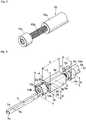
- Fig. 1is a perspective view of a crimp connection terminal of an embodiment according to the invention.
- the crimp connection terminalis made of, for example, thin-walled brass having a thickness of 0.15 mm, and is formed by punching and bending one conductive metal plate plated with copper, tin, etc. on both surfaces.
- connection portion 1corresponding to, for example, a male insertion portion connected to a connection terminal of a counterpart connecter is formed at a front of the crimp connection terminal, and an edge crimping portion 2, a conductor crimping portion 3, and a coated crimping portion 4 are successively disposed on a rear side thereof.
- connection portion 1has a two-layered male insertion end structure in which the conductive metal plate is folded back from both sides and both edges of folded pieces 1a and 1b are butted to each other.
- connection portion 1may correspond to a male connection portion having another shape or a female connection portion.
- a pair of crimping pieces 2a and 2bis raised in a U-shape obliquely upward from both sides of a bottom portion 2c.
- a pair of crimping pieces 3c and 3d having a stacked structure of an upper layer plate 3a and a lower layer plate 3bis raised in a U-shape obliquely upward from both sides.
- the upper layer plate 3ais folded back from the lower layer plate 3b at an upper end, and end edges of the upper layer plate 3a are butted together at a central portion of a bottom portion 3e to form a joint 3f.
- a void 3gwhose cross section corresponds to, for example, a water droplet shape, a balloon shape, a circular shape, an elliptical shape, etc. is provided inside a folded-back portion of the upper layer plate 3a with respect to the lower layer plate 3b at an upper end of each of the crimping pieces 3c and 3d.
- a pair of crimping pieces 4a and 4bis raised in a U-shape obliquely upward from both sides of a bottom portion 4c.
- a stabilizer for stabilizing a posture in a connector housing, a locking portion for preventing coming off from the connector housing in a front-rear direction, etc.may be attached to an actual crimp connection terminal.
- illustration of these known mechanismsis omitted.
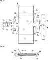
- Fig. 3is a plan view of a state in which a conductive metal plate 5 is punched before being molded into the crimp connection terminal illustrated in Fig. 1 .
- connection portion 1to form an insertion end of a double structure, the folded pieces 1a and 1b serving as upper plates are provided on a bottom portion 1c serving as a lower plate from both sides.
- edge crimping portion 2In the edge crimping portion 2, side portions 2d and 2e serving as the crimping pieces 2a and 2b are projected on both sides of the bottom portion 2c.
- the conductor crimping portion 3includes the lower layer plate 3b disposed at a center and the upper layer plates 3a continuous with both sides of the lower layer plate 3b.
- a dotted lineis an inner fold line at which the upper layer plate 3a is folded back in a forming press described later.
- side portions 4d and 4e serving as the crimping pieces 4a and 4bare projected on both sides of the bottom portion 4c.
- a feed piece 6 for connecting the crimp connection terminals connected in a punched stateis provided further to a rear of the coated crimping portion 4, and the coated crimping portion 4 at a rear end of each crimp connection terminal is connected to the feed piece 6 by a connection piece 7.
- a pilot hole 8 provided in the feed piece 6is used to convey the conductive metal plate 5 in a molding process.
- the conductive metal plate 5 punched out as illustrated in Fig. 3is, for example, successively bent in each molding step by the forming press while being conveyed by the feed piece 6 after being chamfered or surface-treated as necessary, and is molded into the crimp connection terminal illustrated in Fig. 1 . After this molding, the connection piece 7 is cut, and each crimp connection terminal is individually separated.
- Fig. 4is a cross-sectional view of the conductor crimping portion 3 in one process of this bending process, and illustrates a state immediately before the crimping pieces 3c and 3d are raised.
- the void 3gis formed inside a folded-back portion from the lower layer plate 3b of the upper layer plate 3a at a distal end of each of the crimping pieces 3c and 3d.
- a shape of the void 3gcan be set to various shapes . However, it is easy to normally set to shape to a water droplet shape.
- Fig. 5is a perspective view of an electric wire 10 in a state in which an insulating covering portion 10a is peeled off from a conductor portion 10b.
- the electric wire 10 usedis a so-called fiber wire, and is obtained by applying copper plating as metal plating of about a thickness of 1 ⁇ m to an individual core wire including, for example, an aramid fiber filament having a diameter of about 20 ⁇ m and twisting, for example, 130 core wires together.
- a diameter of the conductor portion 10b of the electric wire 10is set to about 0.3 mm
- an outer diameter of the electric wire 10 including the insulating covering portion 10ais set to about 0.7 to 0.8 mm.
- the insulating covering portion 10ais cut and drawn out by a cutter in a circumferential shape, a rear end portion remains at the distal end of the conductor portion 10b, and a front end portion protruding from the conductor portion 10b is cut. Therefore, a remaining portion 10c, which is a part of the insulating covering portion 10a, is attached to the distal end of the exposed conductor portion 10b, and the conductor portion 10b does not come apart.
- Fig. 6is a perspective view of a state in which the electric wire 10 illustrated in Fig. 5 is crimped and fixed by the crimp connection terminal illustrated in Fig. 1 using an electric wire crimping device.
- the remaining portion 10c of the electric wire 10is crimped and fixed by the edge crimping portion 2 together with the conductor portion 10b.
- the conductor portion 10b exposed between the remaining portion 10c and the insulating covering portion 10ais crimped.
- the insulating covering portion 10a of the electric wire 10is crimped and fixed by the coated crimping portion 4.
- a width a of the edge crimping portion 2is about 0.9 mm
- a height b thereofis about 1.2 mm
- a width c of the conductor crimping portion 3is about 1.0 mm
- a height d thereofis about 0.75 mm
- a length e thereofis about 4.5 mm
- a width f of the coated crimping portion 4is about 1.1 mm
- a height g thereofis about 1.5 mm.
- the crimping pieces 3c and 3dhave a two-layer structure of the upper layer plate 3a and the lower layer plate 3b stacked in two layers, and further have the void 3g contributing to elasticity, the crimping pieces 3c and 3d have a large elastic force. Further, when a strong crimping force is applied by the upper press mold Pu and the lower press mold Pd, as illustrated in Fig. 8 , the conductor portion 10b is elastically deformed through the crimping pieces 3c and 3d, the void 3g itself is reduced to be flat, and the conductor portion 10b is firmly tightened and fixed without a gap. In this instance, the upper layer plate 3a in contact with the conductor portion 10b is compressed by being surrounded by the lower layer plate 3b, and thus is sufficiently in close contact with the conductor portion 10b due to occurrence of deformation in which a thickness increases.
- the conductor portion 10b in which a large number of core wires is twisted togethercan be elastically reliably crimped and connected by the crimping pieces 3c and 3d having a two-layer structure and the void 3g.
- the side portions 4d and 4e of the coated crimping portion 4are crimped by being engaged with the insulating covering portion 10a by caulking an outer side of the insulating covering portion 10a of the electric wire 10 using the pair of crimping pieces 4a and 4b. In this way, the insulating covering portion 10a can be fixed to resist a pulling force acting on the electric wire 10.
- Fig. 9illustrates a modification of the conductor crimping portion 3, and a gap 3h is formed at a butted portion of the end edges of the upper layer plate 3a at the bottom portion 3e.
- Fig. 10is a cross-sectional view of a state in which the conductor portion 10b is caulked by the conductor crimping portion 3. A part of the conductor portion 10b is deformed to enter the gap 3h, fixing of the conductor crimping portion 3 with respect to the conductor portion 10b becomes stronger, and an electrical characteristic becomes excellent.
Landscapes
- Engineering & Computer Science (AREA)
- Manufacturing & Machinery (AREA)
- Connections Effected By Soldering, Adhesion, Or Permanent Deformation (AREA)
Description
- The present invention relates to a crimp connection terminal, for example, a crimp connection terminal internally mounted in a connector housing and fit with a connection terminal of a counterpart connector.
- With a recent reduction in size, reduction in weight and integration of an electric product, a smaller connection terminal has been required as a connection terminal used for connection of a circuit. For example, a rectangular insertion portion having a diameter smaller than that of an electric wire to be connected and an outer diameter of about 0.5 mm·0.5 mm is used as a rod-shaped insertion portion inserted into a counterpart connection terminal. In addition, there is a connection terminal used for a fiber wire having a large number of extremely thin core wires.
- In a case in which a fiber wire is crimped to a connection terminal, since a conductor portion of the fiber wire is obtained by forming copper plating around an extremely fine fiber core wire and twisting a plurality of core wires together, the conductor portion is poor in extensibility and plasticity, and highly reliable connection to the fiber wire by the small connection terminal is fairly difficult. When the connection terminal is insufficiently fixed to the fiber wire, the fiber wire is easily pulled out of the connection terminal, and it is difficult to obtain excellent conductivity.
JP-A-2017-162792 US 4142771 A discloses a crimpable terminal device in which the barrel is double walled, with the inner wall being formed from the same sheet of metal as the outer wall.- An object of the invention is to solve the above-mentioned problem, and provide a crimp connection terminal capable of reliably caulking and holding a conductor portion of a fiber wire by a conductor crimping portion having a unique structure and ensuring reliability of electric connection.
- A crimp connection terminal according to the invention for achieving the object is a crimp connection terminal formed by punching and bending one conductive metal plate to caulk and fix an electric wire, wherein a connection portion connected to a connection terminal of a counterpart connecter is disposed at a front side, a conductor crimping portion to crimp and fix a conductor portion of the electric wire is disposed at a rear side, the conductor crimping portion has a pair of crimping pieces raised in a U-shape from a bottom portion, each of the crimping pieces of the conductor crimping portion has a lower layer plate and an upper layer plate formed by folding back from an upper end of the lower layer plate and stacking on the lower layer plate, wherein a void is formed at the folded-back portion between the lower layer plate and the upper layer plate, characterized in that the void (3g) has a cross section corresponding to a water droplet shape, a balloon shape, a circular shape, or an elliptical shape, wherein when a strong crimping force is applied in a crimping process of a conductor portion of an electric wire, upper ends of the crimping pieces (3c, 3d) are closed and the void (3g) is reduced to be flat so that the conductor portion is firmly tightened and fixed without a gap.
- According to the crimp connection terminal according to the invention, it is possible to reliably crimp and connect a conductor portion of a fiber wire in which a plurality of core wires is twisted together to a conductor by a conductor crimping portion and to obtain excellent fixing force and conductivity.
Fig. 1 is a perspective view of a crimp connection terminal of an embodiment.Fig. 2 is a cross-sectional view of a conductor crimping portion.Fig. 3 is a plan view of a punched conductive metal plate.Fig. 4 is a cross-sectional view of the conductor crimping portion in one process of a bending process.Fig. 5 is a perspective view of an electric wire in a state in which a part of an insulating covering portion is left at a distal end.Fig. 6 is a perspective view of the crimp connection terminal in a state in which the electric wire is fixed.Fig. 7 is an explanatory diagram for a crimping process of a conductor portion by the conductor crimping portion.Fig. 8 is a cross-sectional view of the conductor crimping portion in a state in which the conductor portion is fixed.Fig. 9 is a cross-sectional view of a conductor crimping portion according to a modification.Fig. 10 is a cross-sectional view of the conductor crimping portion of the modification in a state in which the conductor portion is fixed.- The invention will be described in detail based on an illustrated embodiment.
Fig. 1 is a perspective view of a crimp connection terminal of an embodiment according to the invention. The crimp connection terminal is made of, for example, thin-walled brass having a thickness of 0.15 mm, and is formed by punching and bending one conductive metal plate plated with copper, tin, etc. on both surfaces.- A
connection portion 1 corresponding to, for example, a male insertion portion connected to a connection terminal of a counterpart connecter is formed at a front of the crimp connection terminal, and anedge crimping portion 2, aconductor crimping portion 3, and a coatedcrimping portion 4 are successively disposed on a rear side thereof. - The
connection portion 1 has a two-layered male insertion end structure in which the conductive metal plate is folded back from both sides and both edges of foldedpieces connection portion 1 may correspond to a male connection portion having another shape or a female connection portion. - In the
edge crimping portion 2, a pair of crimpingpieces bottom portion 2c. - In the
conductor crimping portion 3, as illustrated inFig. 2 , a pair of crimpingpieces upper layer plate 3a and alower layer plate 3b is raised in a U-shape obliquely upward from both sides. Further, theupper layer plate 3a is folded back from thelower layer plate 3b at an upper end, and end edges of theupper layer plate 3a are butted together at a central portion of abottom portion 3e to form ajoint 3f. Avoid 3g whose cross section corresponds to, for example, a water droplet shape, a balloon shape, a circular shape, an elliptical shape, etc. is provided inside a folded-back portion of theupper layer plate 3a with respect to thelower layer plate 3b at an upper end of each of thecrimping pieces - In the coated crimping
portion 4, similarly to theedge crimping portion 2, a pair of crimpingpieces bottom portion 4c. - A stabilizer for stabilizing a posture in a connector housing, a locking portion for preventing coming off from the connector housing in a front-rear direction, etc. may be attached to an actual crimp connection terminal. However, illustration of these known mechanisms is omitted.
Fig. 3 is a plan view of a state in which aconductive metal plate 5 is punched before being molded into the crimp connection terminal illustrated inFig. 1 .- In the
connection portion 1, to form an insertion end of a double structure, the foldedpieces bottom portion 1c serving as a lower plate from both sides. - In the
edge crimping portion 2,side portions pieces bottom portion 2c. - The
conductor crimping portion 3 includes thelower layer plate 3b disposed at a center and theupper layer plates 3a continuous with both sides of thelower layer plate 3b. A dotted line is an inner fold line at which theupper layer plate 3a is folded back in a forming press described later. - In the coated crimping
portion 4,side portions pieces bottom portion 4c. - A
feed piece 6 for connecting the crimp connection terminals connected in a punched state is provided further to a rear of the coatedcrimping portion 4, and the coatedcrimping portion 4 at a rear end of each crimp connection terminal is connected to thefeed piece 6 by a connection piece 7. Apilot hole 8 provided in thefeed piece 6 is used to convey theconductive metal plate 5 in a molding process. - The
conductive metal plate 5 punched out as illustrated inFig. 3 is, for example, successively bent in each molding step by the forming press while being conveyed by thefeed piece 6 after being chamfered or surface-treated as necessary, and is molded into the crimp connection terminal illustrated inFig. 1 . After this molding, the connection piece 7 is cut, and each crimp connection terminal is individually separated. Fig. 4 is a cross-sectional view of theconductor crimping portion 3 in one process of this bending process, and illustrates a state immediately before the crimpingpieces void 3g is formed inside a folded-back portion from thelower layer plate 3b of theupper layer plate 3a at a distal end of each of the crimpingpieces void 3g can be set to various shapes . However, it is easy to normally set to shape to a water droplet shape.Fig. 5 is a perspective view of anelectric wire 10 in a state in which an insulating coveringportion 10a is peeled off from aconductor portion 10b. For example, theelectric wire 10 used is a so-called fiber wire, and is obtained by applying copper plating as metal plating of about a thickness of 1 µm to an individual core wire including, for example, an aramid fiber filament having a diameter of about 20 µm and twisting, for example, 130 core wires together. A diameter of theconductor portion 10b of theelectric wire 10 is set to about 0.3 mm, and an outer diameter of theelectric wire 10 including the insulatingcovering portion 10a is set to about 0.7 to 0.8 mm.- In the
conductor portion 10b, the insulating coveringportion 10a is cut and drawn out by a cutter in a circumferential shape, a rear end portion remains at the distal end of theconductor portion 10b, and a front end portion protruding from theconductor portion 10b is cut. Therefore, aremaining portion 10c, which is a part of the insulating coveringportion 10a, is attached to the distal end of the exposedconductor portion 10b, and theconductor portion 10b does not come apart. Fig. 6 is a perspective view of a state in which theelectric wire 10 illustrated inFig. 5 is crimped and fixed by the crimp connection terminal illustrated inFig. 1 using an electric wire crimping device. Theremaining portion 10c of theelectric wire 10 is crimped and fixed by theedge crimping portion 2 together with theconductor portion 10b. In theconductor crimping portion 3, theconductor portion 10b exposed between theremaining portion 10c and the insulating coveringportion 10a is crimped. The insulating coveringportion 10a of theelectric wire 10 is crimped and fixed by the coatedcrimping portion 4.- With regard to illustrative dimensions of each portion of the crimp connection terminal after crimping the
electric wire 10, a width a of theedge crimping portion 2 is about 0.9 mm, a height b thereof is about 1.2 mm, a width c of theconductor crimping portion 3 is about 1.0 mm, a height d thereof is about 0.75 mm, a length e thereof is about 4.5 mm, a width f of the coatedcrimping portion 4 is about 1.1 mm, and a height g thereof is about 1.5 mm. - In a crimping process of the
conductor portion 10b by the electric wire crimping device, as illustrated in a cross-sectional view ofFig. 7 , in a state in which theconductor portion 10b is inserted between the pair ofcrimping pieces conductor crimping portion 3, upper ends of the crimpingpieces conductor portion 10b is wrapped with the crimpingpieces - Since the crimping
pieces upper layer plate 3a and thelower layer plate 3b stacked in two layers, and further have the void 3g contributing to elasticity, the crimpingpieces Fig. 8 , theconductor portion 10b is elastically deformed through the crimpingpieces conductor portion 10b is firmly tightened and fixed without a gap. In this instance, theupper layer plate 3a in contact with theconductor portion 10b is compressed by being surrounded by thelower layer plate 3b, and thus is sufficiently in close contact with theconductor portion 10b due to occurrence of deformation in which a thickness increases. - As described above, according to the crimp connection terminal of the present embodiment suitable for the fiber wire, the
conductor portion 10b in which a large number of core wires is twisted together can be elastically reliably crimped and connected by the crimpingpieces - In the coated crimping
portion 4, in particular, theside portions portion 4 are crimped by being engaged with the insulatingcovering portion 10a by caulking an outer side of the insulatingcovering portion 10a of theelectric wire 10 using the pair of crimpingpieces covering portion 10a can be fixed to resist a pulling force acting on theelectric wire 10. Fig. 9 illustrates a modification of theconductor crimping portion 3, and agap 3h is formed at a butted portion of the end edges of theupper layer plate 3a at thebottom portion 3e.Fig. 10 is a cross-sectional view of a state in which theconductor portion 10b is caulked by theconductor crimping portion 3. A part of theconductor portion 10b is deformed to enter thegap 3h, fixing of theconductor crimping portion 3 with respect to theconductor portion 10b becomes stronger, and an electrical characteristic becomes excellent.- 1
- Connection portion
- 2
- Edge crimping portion
- 2a, 2b, 3c, 3d, 4a, 4b
- Crimping piece
- 3
- Conductor crimping portion
- 3a
- Upper layer plate
- 3b
- Lower layer plate
- 3e
- Bottom portion
- 3f
- Joint
- 3g
- Void
- 3h
- Gap
- 4
- Coated crimping portion
- 5
- Conductive metal plate
- 10
- Electric wire
- 10a
- Insulating covering portion
- 10b
- Conductor portion
Claims (2)
- A crimp connection terminal formed by punching and bending one conductive metal plate to caulk and fix an electric wire,wherein a connection portion (1) connected to a connection terminal of a counterpart connecter is disposed at a front side, a conductor crimping portion (3) to crimp and fix a conductor portion of the electric wire is disposed at a rear side, the conductor crimping portion (3) has a pair of crimping pieces (3c, 3d) raised in a U-shape from a bottom portion (3e),each of the crimping pieces (3c, 3d) of the conductor crimping portion (3) has a lower layer plate (3b) and an upper layer plate (3a) formed by folding back from an upper end of the lower layer plate (3b) and stacking on the lower layer plate (3b),wherein a void (3g) is formed at the folded-back portion between the lower layer plate (3b) and the upper layer plate (3a),characterized in that the void (3g) has a cross section corresponding to a water droplet shape, a balloon shape, a circular shape, or an elliptical shape, wherein when a strong crimping force is applied in a crimping process of a conductor portion of an electric wire, upper ends of the crimping pieces (3c, 3d) are closed and the void (3g) is reduced to be flat so that the conductor portion is firmly tightened and fixed without a gap.
- The crimp connection terminal according to claim 1, wherein a gap (3h) is provided in a butted portion of end edges of the upper layer plate (3a) on the lower layer plate (3b).
Applications Claiming Priority (1)
| Application Number | Priority Date | Filing Date | Title |
|---|---|---|---|
| JP2018202968AJP6506877B1 (en) | 2018-10-29 | 2018-10-29 | Crimp connection terminal |
Publications (2)
| Publication Number | Publication Date |
|---|---|
| EP3648253A1 EP3648253A1 (en) | 2020-05-06 |
| EP3648253B1true EP3648253B1 (en) | 2022-04-13 |
Family
ID=66324269
Family Applications (1)
| Application Number | Title | Priority Date | Filing Date |
|---|---|---|---|
| EP19197263.7AActiveEP3648253B1 (en) | 2018-10-29 | 2019-09-13 | Crimp connection terminal |
Country Status (4)
| Country | Link |
|---|---|
| US (1) | US10886637B2 (en) |
| EP (1) | EP3648253B1 (en) |
| JP (1) | JP6506877B1 (en) |
| CN (1) | CN111106454B (en) |
Cited By (1)
| Publication number | Priority date | Publication date | Assignee | Title |
|---|---|---|---|---|
| EP4560838A1 (en)* | 2023-11-24 | 2025-05-28 | Union Machinery Co., Ltd. | Conductor crimp structure using connection terminal |
Families Citing this family (4)
| Publication number | Priority date | Publication date | Assignee | Title |
|---|---|---|---|---|
| JP6544412B2 (en)* | 2017-11-22 | 2019-07-17 | オムロン株式会社 | Connector terminals and connectors |
| TWI762255B (en)* | 2021-03-26 | 2022-04-21 | 唐虞企業股份有限公司 | Electrical connector and its conductive terminal |
| DE102022213638A1 (en)* | 2022-12-14 | 2024-06-20 | Robert Bosch Gesellschaft mit beschränkter Haftung | Crimp contact element and connection arrangement |
| JP7499428B1 (en) | 2024-03-13 | 2024-06-13 | ユニオンマシナリ株式会社 | Conductor crimping structure with connection terminal |
Family Cites Families (23)
| Publication number | Priority date | Publication date | Assignee | Title |
|---|---|---|---|---|
| US2783447A (en)* | 1956-03-15 | 1957-02-26 | Aircraft Marine Prod Inc | Electrical connector |
| US3514528A (en)* | 1967-11-13 | 1970-05-26 | Jimmy C Ray | Insulation piercing connector for wires |
| GB1382811A (en)* | 1971-01-11 | 1975-02-05 | Post Office | Clips |
| US3902004A (en)* | 1971-01-11 | 1975-08-26 | Post Office | Clips |
| JPS5138085A (en)* | 1974-09-27 | 1976-03-30 | Yazaki Corp | TANSHIKANAGU |
| US4142771A (en)* | 1974-10-16 | 1979-03-06 | Amp Incorporated | Crimp-type terminal |
| US3916085A (en)* | 1975-01-06 | 1975-10-28 | Essex International Inc | Electrical connector |
| JPS521489A (en)* | 1975-06-24 | 1977-01-07 | Yazaki Corp | Press-attached terminal for aluminium wire |
| JPS5933172Y2 (en)* | 1981-03-12 | 1984-09-17 | 矢崎総業株式会社 | terminal fittings |
| US4692122A (en)* | 1986-10-06 | 1987-09-08 | Minnesota Mining And Manufacturing Company | Electrical terminal |
| JPS6427963U (en)* | 1987-08-12 | 1989-02-17 | ||
| US5445535A (en)* | 1994-05-02 | 1995-08-29 | General Motors Corporation | Insulation displacement terminal |
| FR2858118A1 (en)* | 2003-07-25 | 2005-01-28 | Framatome Connectors Int | Electric crimp contact unit for motor vehicle air bag device, has crimping core having blades and deformable zones for surrounding electrical wire, and tab placed in crimping zone such that tab applies pressure on wire |
| JP5103137B2 (en)* | 2007-11-01 | 2012-12-19 | 株式会社オートネットワーク技術研究所 | Crimp terminal, electric wire with terminal, and manufacturing method thereof |
| JP2009295403A (en)* | 2008-06-04 | 2009-12-17 | Yazaki Corp | Crimp terminal |
| US9397410B2 (en)* | 2010-10-18 | 2016-07-19 | Tyco Electronics Corporation | Electrical terminal for terminating a wire |
| JP5682547B2 (en)* | 2011-12-12 | 2015-03-11 | 株式会社オートネットワーク技術研究所 | Terminal fitting |
| JP5864280B2 (en)* | 2012-01-18 | 2016-02-17 | 矢崎総業株式会社 | Connection method between the flat circuit body and terminal fittings |
| JP6060015B2 (en)* | 2013-03-19 | 2017-01-11 | 矢崎総業株式会社 | Crimp structure for the wire of the crimp terminal |
| JP6039486B2 (en)* | 2013-04-03 | 2016-12-07 | 矢崎総業株式会社 | Terminal connection structure and terminal connection method |
| JP6225313B2 (en) | 2016-03-04 | 2017-11-08 | 株式会社デルタプラス | Crimp connection terminal and manufacturing method thereof |
| WO2017150644A1 (en)* | 2016-03-04 | 2017-09-08 | 三幸電機株式会社 | Crimp connection terminal and production method therefor |
| JP2018147828A (en)* | 2017-03-08 | 2018-09-20 | 株式会社デルタプラス | Crimp connection terminal and method of connecting the crimp connection terminal |
- 2018
- 2018-10-29JPJP2018202968Apatent/JP6506877B1/enactiveActive
- 2019
- 2019-09-13EPEP19197263.7Apatent/EP3648253B1/enactiveActive
- 2019-10-08USUS16/595,579patent/US10886637B2/enactiveActive
- 2019-10-28CNCN201911030129.6Apatent/CN111106454B/enactiveActive
Cited By (1)
| Publication number | Priority date | Publication date | Assignee | Title |
|---|---|---|---|---|
| EP4560838A1 (en)* | 2023-11-24 | 2025-05-28 | Union Machinery Co., Ltd. | Conductor crimp structure using connection terminal |
Also Published As
| Publication number | Publication date |
|---|---|
| EP3648253A1 (en) | 2020-05-06 |
| JP2020071920A (en) | 2020-05-07 |
| US20200136273A1 (en) | 2020-04-30 |
| CN111106454B (en) | 2021-06-01 |
| JP6506877B1 (en) | 2019-04-24 |
| CN111106454A (en) | 2020-05-05 |
| US10886637B2 (en) | 2021-01-05 |
Similar Documents
| Publication | Publication Date | Title |
|---|---|---|
| EP3648253B1 (en) | Crimp connection terminal | |
| US9136628B2 (en) | Crimp type terminal fitting | |
| US7316581B2 (en) | Terminal fitting and method of attaching the same | |
| EP3425735B1 (en) | Crimp connection terminal and production method therefor | |
| WO2010027027A1 (en) | Terminal metal fitting | |
| JP4568210B2 (en) | Terminal metal fittings and flat circuit body with terminals | |
| JP2018147828A (en) | Crimp connection terminal and method of connecting the crimp connection terminal | |
| JP6744975B1 (en) | Crimp connection terminal | |
| JP6858896B1 (en) | Crimping connection terminal | |
| JP6782377B1 (en) | Terminal crimping method to electric wire conductor and crimp connection terminal used in the method | |
| JP4977768B2 (en) | Manufacturing method of multiple types of terminal fittings | |
| JP6506876B1 (en) | Crimp connection terminal | |
| JP6770659B1 (en) | Wire conductor crimping method for connection terminals | |
| EP4560838A1 (en) | Conductor crimp structure using connection terminal | |
| WO2017150644A1 (en) | Crimp connection terminal and production method therefor | |
| JP7504336B1 (en) | Conductor crimping structure with connection terminal | |
| JP7499428B1 (en) | Conductor crimping structure with connection terminal | |
| JPH05211071A (en) | Pressure-welded terminal for electric connector | |
| EP3968473B1 (en) | Method of manufacturing female terminal | |
| CN104347992A (en) | Crimp connector, crimp connector with wires and connection method between the crimp and coated wires | |
| US11296432B2 (en) | Electrical terminal for flat flexible cables | |
| CN115084973A (en) | Processing technology of female terminal, connector and female terminal |
Legal Events
| Date | Code | Title | Description |
|---|---|---|---|
| PUAI | Public reference made under article 153(3) epc to a published international application that has entered the european phase | Free format text:ORIGINAL CODE: 0009012 | |
| STAA | Information on the status of an ep patent application or granted ep patent | Free format text:STATUS: REQUEST FOR EXAMINATION WAS MADE | |
| 17P | Request for examination filed | Effective date:20190913 | |
| AK | Designated contracting states | Kind code of ref document:A1 Designated state(s):AL AT BE BG CH CY CZ DE DK EE ES FI FR GB GR HR HU IE IS IT LI LT LU LV MC MK MT NL NO PL PT RO RS SE SI SK SM TR | |
| AX | Request for extension of the european patent | Extension state:BA ME | |
| RBV | Designated contracting states (corrected) | Designated state(s):AL AT BE BG CH CY CZ DE DK EE ES FI FR GB GR HR HU IE IS IT LI LT LU LV MC MK MT NL NO PL PT RO RS SE SI SK SM TR | |
| GRAP | Despatch of communication of intention to grant a patent | Free format text:ORIGINAL CODE: EPIDOSNIGR1 | |
| STAA | Information on the status of an ep patent application or granted ep patent | Free format text:STATUS: GRANT OF PATENT IS INTENDED | |
| INTG | Intention to grant announced | Effective date:20211124 | |
| GRAS | Grant fee paid | Free format text:ORIGINAL CODE: EPIDOSNIGR3 | |
| GRAA | (expected) grant | Free format text:ORIGINAL CODE: 0009210 | |
| STAA | Information on the status of an ep patent application or granted ep patent | Free format text:STATUS: THE PATENT HAS BEEN GRANTED | |
| AK | Designated contracting states | Kind code of ref document:B1 Designated state(s):AL AT BE BG CH CY CZ DE DK EE ES FI FR GB GR HR HU IE IS IT LI LT LU LV MC MK MT NL NO PL PT RO RS SE SI SK SM TR | |
| REG | Reference to a national code | Ref country code:GB Ref legal event code:FG4D | |
| REG | Reference to a national code | Ref country code:CH Ref legal event code:EP | |
| REG | Reference to a national code | Ref country code:DE Ref legal event code:R096 Ref document number:602019013631 Country of ref document:DE | |
| REG | Reference to a national code | Ref country code:IE Ref legal event code:FG4D | |
| REG | Reference to a national code | Ref country code:AT Ref legal event code:REF Ref document number:1484133 Country of ref document:AT Kind code of ref document:T Effective date:20220515 | |
| REG | Reference to a national code | Ref country code:LT Ref legal event code:MG9D | |
| REG | Reference to a national code | Ref country code:NL Ref legal event code:MP Effective date:20220413 | |
| REG | Reference to a national code | Ref country code:AT Ref legal event code:MK05 Ref document number:1484133 Country of ref document:AT Kind code of ref document:T Effective date:20220413 | |
| PG25 | Lapsed in a contracting state [announced via postgrant information from national office to epo] | Ref country code:NL Free format text:LAPSE BECAUSE OF FAILURE TO SUBMIT A TRANSLATION OF THE DESCRIPTION OR TO PAY THE FEE WITHIN THE PRESCRIBED TIME-LIMIT Effective date:20220413 | |
| PG25 | Lapsed in a contracting state [announced via postgrant information from national office to epo] | Ref country code:SE Free format text:LAPSE BECAUSE OF FAILURE TO SUBMIT A TRANSLATION OF THE DESCRIPTION OR TO PAY THE FEE WITHIN THE PRESCRIBED TIME-LIMIT Effective date:20220413 Ref country code:PT Free format text:LAPSE BECAUSE OF FAILURE TO SUBMIT A TRANSLATION OF THE DESCRIPTION OR TO PAY THE FEE WITHIN THE PRESCRIBED TIME-LIMIT Effective date:20220816 Ref country code:NO Free format text:LAPSE BECAUSE OF FAILURE TO SUBMIT A TRANSLATION OF THE DESCRIPTION OR TO PAY THE FEE WITHIN THE PRESCRIBED TIME-LIMIT Effective date:20220713 Ref country code:LT Free format text:LAPSE BECAUSE OF FAILURE TO SUBMIT A TRANSLATION OF THE DESCRIPTION OR TO PAY THE FEE WITHIN THE PRESCRIBED TIME-LIMIT Effective date:20220413 Ref country code:HR Free format text:LAPSE BECAUSE OF FAILURE TO SUBMIT A TRANSLATION OF THE DESCRIPTION OR TO PAY THE FEE WITHIN THE PRESCRIBED TIME-LIMIT Effective date:20220413 Ref country code:GR Free format text:LAPSE BECAUSE OF FAILURE TO SUBMIT A TRANSLATION OF THE DESCRIPTION OR TO PAY THE FEE WITHIN THE PRESCRIBED TIME-LIMIT Effective date:20220714 Ref country code:FI Free format text:LAPSE BECAUSE OF FAILURE TO SUBMIT A TRANSLATION OF THE DESCRIPTION OR TO PAY THE FEE WITHIN THE PRESCRIBED TIME-LIMIT Effective date:20220413 Ref country code:ES Free format text:LAPSE BECAUSE OF FAILURE TO SUBMIT A TRANSLATION OF THE DESCRIPTION OR TO PAY THE FEE WITHIN THE PRESCRIBED TIME-LIMIT Effective date:20220413 Ref country code:BG Free format text:LAPSE BECAUSE OF FAILURE TO SUBMIT A TRANSLATION OF THE DESCRIPTION OR TO PAY THE FEE WITHIN THE PRESCRIBED TIME-LIMIT Effective date:20220713 Ref country code:AT Free format text:LAPSE BECAUSE OF FAILURE TO SUBMIT A TRANSLATION OF THE DESCRIPTION OR TO PAY THE FEE WITHIN THE PRESCRIBED TIME-LIMIT Effective date:20220413 | |
| PG25 | Lapsed in a contracting state [announced via postgrant information from national office to epo] | Ref country code:RS Free format text:LAPSE BECAUSE OF FAILURE TO SUBMIT A TRANSLATION OF THE DESCRIPTION OR TO PAY THE FEE WITHIN THE PRESCRIBED TIME-LIMIT Effective date:20220413 Ref country code:PL Free format text:LAPSE BECAUSE OF FAILURE TO SUBMIT A TRANSLATION OF THE DESCRIPTION OR TO PAY THE FEE WITHIN THE PRESCRIBED TIME-LIMIT Effective date:20220413 Ref country code:LV Free format text:LAPSE BECAUSE OF FAILURE TO SUBMIT A TRANSLATION OF THE DESCRIPTION OR TO PAY THE FEE WITHIN THE PRESCRIBED TIME-LIMIT Effective date:20220413 Ref country code:IS Free format text:LAPSE BECAUSE OF FAILURE TO SUBMIT A TRANSLATION OF THE DESCRIPTION OR TO PAY THE FEE WITHIN THE PRESCRIBED TIME-LIMIT Effective date:20220813 | |
| REG | Reference to a national code | Ref country code:DE Ref legal event code:R097 Ref document number:602019013631 Country of ref document:DE | |
| PG25 | Lapsed in a contracting state [announced via postgrant information from national office to epo] | Ref country code:SM Free format text:LAPSE BECAUSE OF FAILURE TO SUBMIT A TRANSLATION OF THE DESCRIPTION OR TO PAY THE FEE WITHIN THE PRESCRIBED TIME-LIMIT Effective date:20220413 Ref country code:SK Free format text:LAPSE BECAUSE OF FAILURE TO SUBMIT A TRANSLATION OF THE DESCRIPTION OR TO PAY THE FEE WITHIN THE PRESCRIBED TIME-LIMIT Effective date:20220413 Ref country code:RO Free format text:LAPSE BECAUSE OF FAILURE TO SUBMIT A TRANSLATION OF THE DESCRIPTION OR TO PAY THE FEE WITHIN THE PRESCRIBED TIME-LIMIT Effective date:20220413 Ref country code:EE Free format text:LAPSE BECAUSE OF FAILURE TO SUBMIT A TRANSLATION OF THE DESCRIPTION OR TO PAY THE FEE WITHIN THE PRESCRIBED TIME-LIMIT Effective date:20220413 Ref country code:DK Free format text:LAPSE BECAUSE OF FAILURE TO SUBMIT A TRANSLATION OF THE DESCRIPTION OR TO PAY THE FEE WITHIN THE PRESCRIBED TIME-LIMIT Effective date:20220413 Ref country code:CZ Free format text:LAPSE BECAUSE OF FAILURE TO SUBMIT A TRANSLATION OF THE DESCRIPTION OR TO PAY THE FEE WITHIN THE PRESCRIBED TIME-LIMIT Effective date:20220413 | |
| PLBE | No opposition filed within time limit | Free format text:ORIGINAL CODE: 0009261 | |
| STAA | Information on the status of an ep patent application or granted ep patent | Free format text:STATUS: NO OPPOSITION FILED WITHIN TIME LIMIT | |
| 26N | No opposition filed | Effective date:20230116 | |
| PG25 | Lapsed in a contracting state [announced via postgrant information from national office to epo] | Ref country code:AL Free format text:LAPSE BECAUSE OF FAILURE TO SUBMIT A TRANSLATION OF THE DESCRIPTION OR TO PAY THE FEE WITHIN THE PRESCRIBED TIME-LIMIT Effective date:20220413 | |
| PG25 | Lapsed in a contracting state [announced via postgrant information from national office to epo] | Ref country code:MC Free format text:LAPSE BECAUSE OF FAILURE TO SUBMIT A TRANSLATION OF THE DESCRIPTION OR TO PAY THE FEE WITHIN THE PRESCRIBED TIME-LIMIT Effective date:20220413 | |
| REG | Reference to a national code | Ref country code:CH Ref legal event code:PL | |
| REG | Reference to a national code | Ref country code:BE Ref legal event code:MM Effective date:20220930 | |
| PG25 | Lapsed in a contracting state [announced via postgrant information from national office to epo] | Ref country code:SI Free format text:LAPSE BECAUSE OF FAILURE TO SUBMIT A TRANSLATION OF THE DESCRIPTION OR TO PAY THE FEE WITHIN THE PRESCRIBED TIME-LIMIT Effective date:20220413 | |
| PG25 | Lapsed in a contracting state [announced via postgrant information from national office to epo] | Ref country code:LU Free format text:LAPSE BECAUSE OF NON-PAYMENT OF DUE FEES Effective date:20220913 | |
| PG25 | Lapsed in a contracting state [announced via postgrant information from national office to epo] | Ref country code:LI Free format text:LAPSE BECAUSE OF NON-PAYMENT OF DUE FEES Effective date:20220930 Ref country code:IE Free format text:LAPSE BECAUSE OF NON-PAYMENT OF DUE FEES Effective date:20220913 Ref country code:CH Free format text:LAPSE BECAUSE OF NON-PAYMENT OF DUE FEES Effective date:20220930 | |
| PG25 | Lapsed in a contracting state [announced via postgrant information from national office to epo] | Ref country code:BE Free format text:LAPSE BECAUSE OF NON-PAYMENT OF DUE FEES Effective date:20220930 | |
| PG25 | Lapsed in a contracting state [announced via postgrant information from national office to epo] | Ref country code:IT Free format text:LAPSE BECAUSE OF FAILURE TO SUBMIT A TRANSLATION OF THE DESCRIPTION OR TO PAY THE FEE WITHIN THE PRESCRIBED TIME-LIMIT Effective date:20220413 | |
| PG25 | Lapsed in a contracting state [announced via postgrant information from national office to epo] | Ref country code:HU Free format text:LAPSE BECAUSE OF FAILURE TO SUBMIT A TRANSLATION OF THE DESCRIPTION OR TO PAY THE FEE WITHIN THE PRESCRIBED TIME-LIMIT; INVALID AB INITIO Effective date:20190913 | |
| PG25 | Lapsed in a contracting state [announced via postgrant information from national office to epo] | Ref country code:CY Free format text:LAPSE BECAUSE OF FAILURE TO SUBMIT A TRANSLATION OF THE DESCRIPTION OR TO PAY THE FEE WITHIN THE PRESCRIBED TIME-LIMIT Effective date:20220413 | |
| GBPC | Gb: european patent ceased through non-payment of renewal fee | Effective date:20230913 | |
| PG25 | Lapsed in a contracting state [announced via postgrant information from national office to epo] | Ref country code:MK Free format text:LAPSE BECAUSE OF FAILURE TO SUBMIT A TRANSLATION OF THE DESCRIPTION OR TO PAY THE FEE WITHIN THE PRESCRIBED TIME-LIMIT Effective date:20220413 | |
| PG25 | Lapsed in a contracting state [announced via postgrant information from national office to epo] | Ref country code:GB Free format text:LAPSE BECAUSE OF NON-PAYMENT OF DUE FEES Effective date:20230913 | |
| PG25 | Lapsed in a contracting state [announced via postgrant information from national office to epo] | Ref country code:GB Free format text:LAPSE BECAUSE OF NON-PAYMENT OF DUE FEES Effective date:20230913 | |
| PG25 | Lapsed in a contracting state [announced via postgrant information from national office to epo] | Ref country code:MT Free format text:LAPSE BECAUSE OF FAILURE TO SUBMIT A TRANSLATION OF THE DESCRIPTION OR TO PAY THE FEE WITHIN THE PRESCRIBED TIME-LIMIT Effective date:20220413 | |
| PGFP | Annual fee paid to national office [announced via postgrant information from national office to epo] | Ref country code:DE Payment date:20240918 Year of fee payment:6 | |
| PGFP | Annual fee paid to national office [announced via postgrant information from national office to epo] | Ref country code:FR Payment date:20240925 Year of fee payment:6 | |
| PG25 | Lapsed in a contracting state [announced via postgrant information from national office to epo] | Ref country code:BG Free format text:LAPSE BECAUSE OF FAILURE TO SUBMIT A TRANSLATION OF THE DESCRIPTION OR TO PAY THE FEE WITHIN THE PRESCRIBED TIME-LIMIT Effective date:20220413 | |
| PG25 | Lapsed in a contracting state [announced via postgrant information from national office to epo] | Ref country code:BG Free format text:LAPSE BECAUSE OF FAILURE TO SUBMIT A TRANSLATION OF THE DESCRIPTION OR TO PAY THE FEE WITHIN THE PRESCRIBED TIME-LIMIT Effective date:20220413 |