EP3647737B1 - Sensor interface circuit - Google Patents
Sensor interface circuitDownload PDFInfo
- Publication number
- EP3647737B1 EP3647737B1EP18204290.3AEP18204290AEP3647737B1EP 3647737 B1EP3647737 B1EP 3647737B1EP 18204290 AEP18204290 AEP 18204290AEP 3647737 B1EP3647737 B1EP 3647737B1
- Authority
- EP
- European Patent Office
- Prior art keywords
- sensor
- signal
- interface circuit
- result
- characterisation data
- Prior art date
- Legal status (The legal status is an assumption and is not a legal conclusion. Google has not performed a legal analysis and makes no representation as to the accuracy of the status listed.)
- Active
Links
- 238000012512characterization methodMethods0.000claimsdescription29
- 238000006243chemical reactionMethods0.000claimsdescription18
- 238000012545processingMethods0.000claimsdescription18
- 230000006854communicationEffects0.000claimsdescription16
- 238000004891communicationMethods0.000claimsdescription16
- 238000000034methodMethods0.000claimsdescription13
- 230000007175bidirectional communicationEffects0.000claims1
- 238000004364calculation methodMethods0.000description12
- 230000008901benefitEffects0.000description8
- 239000012528membraneSubstances0.000description7
- 238000012546transferMethods0.000description5
- 230000008859changeEffects0.000description4
- 230000000704physical effectEffects0.000description4
- 238000005259measurementMethods0.000description3
- 230000008569processEffects0.000description3
- 239000012491analyteSubstances0.000description2
- 230000002457bidirectional effectEffects0.000description2
- 230000005540biological transmissionEffects0.000description2
- 238000004422calculation algorithmMethods0.000description2
- 230000001419dependent effectEffects0.000description2
- 238000013461designMethods0.000description2
- 238000005516engineering processMethods0.000description2
- 238000011156evaluationMethods0.000description2
- 238000012360testing methodMethods0.000description2
- XUIMIQQOPSSXEZ-UHFFFAOYSA-NSiliconChemical compound[Si]XUIMIQQOPSSXEZ-UHFFFAOYSA-N0.000description1
- 230000003321amplificationEffects0.000description1
- 238000013459approachMethods0.000description1
- 230000006399behaviorEffects0.000description1
- 230000009286beneficial effectEffects0.000description1
- 230000002860competitive effectEffects0.000description1
- 238000004590computer programMethods0.000description1
- 238000012937correctionMethods0.000description1
- 230000008878couplingEffects0.000description1
- 238000010168coupling processMethods0.000description1
- 238000005859coupling reactionMethods0.000description1
- 238000011143downstream manufacturingMethods0.000description1
- 238000001914filtrationMethods0.000description1
- 230000006870functionEffects0.000description1
- 230000036541healthEffects0.000description1
- 230000007246mechanismEffects0.000description1
- 238000003199nucleic acid amplification methodMethods0.000description1
- 230000003287optical effectEffects0.000description1
- 239000000523sampleSubstances0.000description1
- 230000035945sensitivityEffects0.000description1
- 229910052710siliconInorganic materials0.000description1
- 239000010703siliconSubstances0.000description1
Images


Classifications
- G—PHYSICS
- G01—MEASURING; TESTING
- G01D—MEASURING NOT SPECIALLY ADAPTED FOR A SPECIFIC VARIABLE; ARRANGEMENTS FOR MEASURING TWO OR MORE VARIABLES NOT COVERED IN A SINGLE OTHER SUBCLASS; TARIFF METERING APPARATUS; MEASURING OR TESTING NOT OTHERWISE PROVIDED FOR
- G01D3/00—Indicating or recording apparatus with provision for the special purposes referred to in the subgroups
- G—PHYSICS
- G01—MEASURING; TESTING
- G01R—MEASURING ELECTRIC VARIABLES; MEASURING MAGNETIC VARIABLES
- G01R19/00—Arrangements for measuring currents or voltages or for indicating presence or sign thereof
- G01R19/25—Arrangements for measuring currents or voltages or for indicating presence or sign thereof using digital measurement techniques
- G01R19/252—Arrangements for measuring currents or voltages or for indicating presence or sign thereof using digital measurement techniques using analogue/digital converters of the type with conversion of voltage or current into frequency and measuring of this frequency
- G—PHYSICS
- G01—MEASURING; TESTING
- G01D—MEASURING NOT SPECIALLY ADAPTED FOR A SPECIFIC VARIABLE; ARRANGEMENTS FOR MEASURING TWO OR MORE VARIABLES NOT COVERED IN A SINGLE OTHER SUBCLASS; TARIFF METERING APPARATUS; MEASURING OR TESTING NOT OTHERWISE PROVIDED FOR
- G01D18/00—Testing or calibrating apparatus or arrangements provided for in groups G01D1/00 - G01D15/00
- G01D18/008—Testing or calibrating apparatus or arrangements provided for in groups G01D1/00 - G01D15/00 with calibration coefficients stored in memory
- G—PHYSICS
- G01—MEASURING; TESTING
- G01D—MEASURING NOT SPECIALLY ADAPTED FOR A SPECIFIC VARIABLE; ARRANGEMENTS FOR MEASURING TWO OR MORE VARIABLES NOT COVERED IN A SINGLE OTHER SUBCLASS; TARIFF METERING APPARATUS; MEASURING OR TESTING NOT OTHERWISE PROVIDED FOR
- G01D3/00—Indicating or recording apparatus with provision for the special purposes referred to in the subgroups
- G01D3/02—Indicating or recording apparatus with provision for the special purposes referred to in the subgroups with provision for altering or correcting the law of variation
- G01D3/022—Indicating or recording apparatus with provision for the special purposes referred to in the subgroups with provision for altering or correcting the law of variation having an ideal characteristic, map or correction data stored in a digital memory
- G—PHYSICS
- G01—MEASURING; TESTING
- G01D—MEASURING NOT SPECIALLY ADAPTED FOR A SPECIFIC VARIABLE; ARRANGEMENTS FOR MEASURING TWO OR MORE VARIABLES NOT COVERED IN A SINGLE OTHER SUBCLASS; TARIFF METERING APPARATUS; MEASURING OR TESTING NOT OTHERWISE PROVIDED FOR
- G01D3/00—Indicating or recording apparatus with provision for the special purposes referred to in the subgroups
- G01D3/028—Indicating or recording apparatus with provision for the special purposes referred to in the subgroups mitigating undesired influences, e.g. temperature, pressure
- G01D3/036—Indicating or recording apparatus with provision for the special purposes referred to in the subgroups mitigating undesired influences, e.g. temperature, pressure on measuring arrangements themselves
- G—PHYSICS
- G01—MEASURING; TESTING
- G01D—MEASURING NOT SPECIALLY ADAPTED FOR A SPECIFIC VARIABLE; ARRANGEMENTS FOR MEASURING TWO OR MORE VARIABLES NOT COVERED IN A SINGLE OTHER SUBCLASS; TARIFF METERING APPARATUS; MEASURING OR TESTING NOT OTHERWISE PROVIDED FOR
- G01D5/00—Mechanical means for transferring the output of a sensing member; Means for converting the output of a sensing member to another variable where the form or nature of the sensing member does not constrain the means for converting; Transducers not specially adapted for a specific variable
- G01D5/12—Mechanical means for transferring the output of a sensing member; Means for converting the output of a sensing member to another variable where the form or nature of the sensing member does not constrain the means for converting; Transducers not specially adapted for a specific variable using electric or magnetic means
- G01D5/14—Mechanical means for transferring the output of a sensing member; Means for converting the output of a sensing member to another variable where the form or nature of the sensing member does not constrain the means for converting; Transducers not specially adapted for a specific variable using electric or magnetic means influencing the magnitude of a current or voltage
- G01D5/16—Mechanical means for transferring the output of a sensing member; Means for converting the output of a sensing member to another variable where the form or nature of the sensing member does not constrain the means for converting; Transducers not specially adapted for a specific variable using electric or magnetic means influencing the magnitude of a current or voltage by varying resistance
- G—PHYSICS
- G01—MEASURING; TESTING
- G01R—MEASURING ELECTRIC VARIABLES; MEASURING MAGNETIC VARIABLES
- G01R31/00—Arrangements for testing electric properties; Arrangements for locating electric faults; Arrangements for electrical testing characterised by what is being tested not provided for elsewhere
- G01R31/28—Testing of electronic circuits, e.g. by signal tracer
- G01R31/282—Testing of electronic circuits specially adapted for particular applications not provided for elsewhere
- G01R31/2829—Testing of circuits in sensor or actuator systems
- G—PHYSICS
- G01—MEASURING; TESTING
- G01R—MEASURING ELECTRIC VARIABLES; MEASURING MAGNETIC VARIABLES
- G01R31/00—Arrangements for testing electric properties; Arrangements for locating electric faults; Arrangements for electrical testing characterised by what is being tested not provided for elsewhere
- G01R31/28—Testing of electronic circuits, e.g. by signal tracer
- G01R31/317—Testing of digital circuits
- H—ELECTRICITY
- H03—ELECTRONIC CIRCUITRY
- H03M—CODING; DECODING; CODE CONVERSION IN GENERAL
- H03M1/00—Analogue/digital conversion; Digital/analogue conversion
- H03M1/12—Analogue/digital converters
- H03M1/1205—Multiplexed conversion systems
Definitions
- the present inventionis generally related to the field of sensor interfaces for sensor systems.
- Sensorsare increasingly important in any field where finer and ever more intelligent control is needed. Examples are found in the growing fields of automotive applications or wireless sensor networks (WSN). In the automotive industry sensors are essential for applications ranging from increased safety to road stability as well as to improve car performance and reliability demanded by customers. Further, compact and low-power sensor interfaces are needed to be competitive on the growing market and to enable new applications for the 'Internet of things'.
- WSNwireless sensor networks
- the silicon areais a main contributor to the cost of the sensor interface, therefore the interface has to be made as small as possible. This should not only be valid for the technology nodes that are used today (and which are still relative big for the automotive industry), but also in more advanced technologies.
- a wrong readout by a sensorcan put the driver and his/her surroundings in danger. As such, the sensor's signal should either be correct or flagged as wrong. The system either trusts the signal or discards the signal.
- a popular, but expensive way to diagnose a sensor's healthis by comparing the signal of multiple sensors.
- decomposing one readout by multiple non-identical sensorscan improve safety. Using non-identical sensors can be crucial as common mode failures cannot always be detected. Consider, for example, two cameras in a foggy situation. Their readout is less trustworthy than one camera and radar.
- IC sensor diagnostics using multiple (e.g., redundant) communication signal pathsare presented, wherein one or more of the communication signal paths can be diverse (e.g., in hardware, software or processing, in operating principle or in some other way) from at least one other of the multiple communication signal paths.
- US9863786discloses a solution where the different paths use different data representations.
- the sensor elementscan operate to communicate respective signal components having different data representations, such as different trigonometric representations, inverse representations with respect to one another, different addends of a sum or other different proportional or inverse proportional representations with respect to one another.
- Application US2013/200909relates to a fully integrated sensor device where two separate signal paths enable functional safety.
- a crucial aspect about this integrated deviceis that the sense element is part of the integrated circuit.
- US2004/075447is concerned with a low cost sensor interface IC with two identical signal paths.
- the sense elementis a pressure sensitive membrane with four piezo resistive components.
- Most designsuse a full bridge where all four piezo resistances enable one readout signal path.
- This designuses two half bridges, where two out of four piezo-resistances enable one readout and the other two out of four piezo resistances enable the other readout.
- US2009/177056discloses an analyte monitor including a sensor, a sensor control unit and a display unit.
- the sensor control unithas a housing that can be placed on skin and receive a portion of an electrochemical sensor.
- the sensor control unitalso includes conductive contacts disposed on the housing and configured for coupling to two or more contact pads on the sensor.
- a transmitteris disposed in the housing and coupled to the conductive contacts for transmitting data obtained using the sensor.
- the display unithas a receiver for receiving data from the transmitter and a display coupled to the receiver for displaying an indication of a level of an analyte.
- Application US2018/266856presents an interface device to be connected between an electronic instrument and a smart measurement probe providing information regarding calibration data, with the ability to generate simulated sensor outputs.
- a transmitter interrogation process utilizing these simulated sensor outputsmay be used to determine the transmitter settings and provide an emulated sensor output emulating a previous sensor-transmitter pairing.
- the inventionrelates to system as defined in claim 1.
- the proposed sensor interface circuitindeed allows for use in safety critical applications.
- One sensor resultis calculated in the sensor interface circuit and next output to a further device of the application along with the digital signal derived from the sensor signal and with the sensor characterisation data.
- the sensor interface circuitso provides that further device with all required information to determine a second sensor result using different processing means than the processing means used in the sensor interface circuit to obtain said first sensor result.
- the further devicecan then compare the first and the second sensor result and so verify their reliability.
- said output unitis connectable to a communication bus.
- the communication busis bidirectional.
- the output unitis arranged for time multiplexing the first sensor result, the digitized version of the sensor signal and the sensor characterisation data.
- the conversion meanscomprises a filter and/or an amplifier.
- the sensor interface circuitcomprises separate conversion means for a first signal path comprising the processing means and for a second signal path guiding the digital signal to the output unit.
- the inputis arranged to receive two sensor signals from the sensor, whereby each sensor signal is applied to a different one of said separate conversion means.
- the inputis arranged to receive an additional sensor signal from an additional sensor.
- an additional sensor signalfrom an additional sensor.
- the sensor interface circuitmay comprise a further memory to store separately the sensor characterisation data to be output by the output unit.
- the sensor interface circuitcomprises a sensor arranged to convert the physical quantity into the electrical quantity and to output the sensor signal.
- the sensor interface circuitis arranged to derive temperature information and to output that temperature information.
- the inventionrelates to a method as defined in claim 12.
- the methodfurther comprises a step of which of the first and second sensor result is most trustworthy.
- the most trustworthy sensor resultmay be determined by exploiting at least one additional signal path.
- the external control unitsends a request to receive the sensor characterisation data to the sensor interface circuit.
- a sensorconverts a physical quantity into an analog electrical quantity.
- the sensor output signalis too small to be used directly. Therefore a sensor interface circuit amplifies the signal comprising the electrical quantity received from the sensor to obtain a more useful signal.
- the signalis often also further processed (e.g. filtered) in the sensor interface. Additionally the signal is converted to a digital signal and further processed in the digital domain.
- a sensor interface circuitis considered to be a structure to transfer the electrical quantity coming out of the sensor into a digital signal.
- the input signal containing the physical quantity to be converted in the sensoroften represents a pressure, temperature or magnetic field, also other types of physical signals can be used as input to the interface circuit of this invention.
- the sensor interface circuit of the inventionmay have the sensor as a part of the interface circuit, this is not strictly required.
- the sensor(s)may be external to the circuit of the invention and the circuit is fed with an electrical signal representative of the electrical quantity into which the physical quantity is converted in the sensor.
- the present inventiondiscloses a sensor interface circuit comprising one signal path where a first sensor result is calculated. The resulting signal and the information required to perform a second calculation is then outputted. This second calculation is performed outside the sensor interface circuit. As also the outcome of the first calculation is outputted to a further device of the application, the latter is capable of comparing the two results.
- the sensor interface circuit of this inventionis typically used in safety critical applications.
- the sensor interface circuitreceives from the sensing element the analog electrical signal to which the physical quantity was converted.
- the analog signalis fed to a conversion block of the sensor interface circuit and outputs a digitized version of that electrical signal, which is subsequently employed by another device in the application, e.g. in an Engine Control Unit (ECU).
- ECUEngine Control Unit
- the sensor elementitself does not have to be part of the sensor interface's integrated circuit, but the signal output by the sensor is applied to the sensor interface.
- the characterization information of the sensoris needed.
- a membrane for pressure sensor readoutis a membrane for pressure sensor readout.
- the resistances of the piezo-resistive bridge on this membranechange according to the pressure sensed by the membrane. Each resistance is also affected by the process variations.
- the sensor elementis distinct from the interface but the bridge nodes are connected to the interface.
- the safety critical applicationcan be e.g. the electronic stability control system of a car, i.e. the interface is connected to an ECU of the vehicle.
- the sensor characterisation datae.g. in the form of calibration coefficients
- This datais used in the first signal path to calculate the first signal result.
- the sensor characterisation datais transferred to another device used in the application, e.g. an engine control unit.
- These correction coefficientsare subsequently used to process the digital signal in the second signal path outside the sensor interface circuit.
- the digital protocol applied to transfer data from the sensor interface to the ECUcan transmit these coefficients during initialization of the device. Also after initialization these coefficients can be sent regularly at a slow pace. Furthermore also temperature information (or any other parameter that has an influence on the sensor output) may be sent. This should not be sent only during initialization, but at regular time instants. Typically this can also be done at a slow pace, because temperature does not change so quickly.
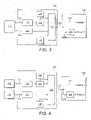
- the sensor system 100 in Fig.1comprises a sense element 110, a sensor interface circuit 120 and an ECU 140. While the resulting signal in one of the two signal paths 131, 132 is calculated in the sensor interface 120, the calculation of the other is performed in a separate unit 140 (in the ECU in this example). So, the sensor interface 120 fully calculates signal Result 1, whereas signal Result 2 is calculated at least partially in the ECU.
- a signal processor unit 128like e.g. a digital signal processor (DSP) or a microcontroller in the sensor interface to perform the calculations for the first signal result and a signal processing unit 148 in or connected with unit 140 to perform the calculations for the second signal result.
- the signal processor unitscan be similar or have different implementations.
- the sensor element signalis an analogue signal, it requires a conversion block 123.
- the conversion blockcomprises at least a conversion means to digitize the analogue signal, like an Analogue-to-Digital Converter (ADC), a time-to-digital converter or a sensor-to-digital converter.
- ADCAnalogue-to-Digital Converter
- filtering means and/or amplification meanscan be provided in the conversion block.
- the signal obtained at the output of the conversion blockis a digital signal.
- the digital signalis used for the calculations in the DSP block 128 of the sensor interface circuit.
- the DSP 128is operably connected with the memory 125 where the calibration coefficients are stored, so that the DSP can obtain the coefficients needed for the calculations.
- DSP 128is further operably connected to a communication unit 122. This communication unit is via a communication bus 133 connected with the ECU 140. The bus is used for transferring the calculated result for the first signal path (Signal result1) as well as the input for performing the second calculation.
- the digital signalis directly fed to the communication unit 122.
- the sensor characterisation data(e.g. the calibration coefficients) are available in the memory 125, which is, as already said, operably connected to the communication unit.
- a separate memory for the second signal pathis provided, which is obviously also operably connected to the communication unit 122. This is shown in Fig.2 .
- the communication unitis used for transmitting the digital signal and the stored sensor characterisation data to the ECU 140 using the communication bus 133.
- the sensor characterisation datais transferred only when the coefficients in the memory need an update.
- One option to transfer the sensor characterisation data to the ECUis by means of a popular protocol like SENT. This protocol typically works with a slow and a fast message, whereby the necessary memory data is sent to the ECU in several slow channel messages. For example, signal Result 1 and the raw sensor signal in the second signal path are sent each frame and 18 frames are needed to build a slow message. So, it takes about 1 ms to transfer one fast message and 18ms to transfer one slow message.
- the sensor characterisation datamay be sent in the first slow channel messages exchanged between the sensor interface circuit and the ECU. If the ECU detects this sensor characterisation data is new, it waits until all new data (e.g. calibration coefficients) has been received. If the characterisation data is found to be already stored in the ECU, the ECU can immediately start and calculate the signal Result2 for the second path 132 using the DSP block 148 in the ECU.
- temperature informationis transmitted e.g. using such a slow channel.
- the temperature informationis often derived from the total resistance of a bridge of resistors (which is not changing much with pressure, because typically two resistors increase with pressure, while the other two decrease which pressure).
- a temperature sensoris provided on the interface circuit itself (e.g. bandgap based). It represents very well the pressure sensor temperature when the pressure sensor is part of the interface die or when both dies are in the same package.
- Fig.1there is a single conversion means.
- the sensorprovides two separate signals which are applied to separate conversion blocks (123,124) provided for a first and a second signal path. This is illustrated in Fig.2 .
- the sensing element 110 in the embodiment of Fig.3outputs two separate signals to two distinct conversion blocks.
- Fig.4shows a variant of Fig.3 , whereby two different sensing elements (110,111) are used, each feeding one of the signal paths. Having two distinct sensors may be beneficial because otherwise a single error in the sensor can make both signal results corrupt.
- One optionis to use twice the same sensor, but this is expensive and might not be good enough because of common cause failures.
- the membranecan be common for both sensors, but different resistors are used. This assumes a very reliable membrane.
- One of the sensorscan use a full bridge, while the other is using only a half bridge.
- Onecan also differentiate in the type of resistor used.
- Onecan have a resistive and a capacitive sensor to have true diversity. For a MEMS pressure sensor the size of the membrane (and so the sensitivity) and the shape (square versus round) can be varied.
- a key feature of the present inventionis the storage of the sensor characterisation data in the memory 125 (and optionally memory 126) of the sensor interface circuit and performing the calculation of the second signal result in the ECU after the characterisation data is transferred from the sensor interface to ECU. Note that in case the memory 126 is present, the connection of the other memory 125 to the communication unit 122 is not strictly needed, as memory 126 is then used for transferring the sensor characterisation data .
- the main advantage of storing the coefficients for the ECU calculations in the sensor interfaceis that the calibration of the sensor and sensor interface circuit can be done without ECU. So it can be done by the provider of the sensor and sensor interface. Furthermore it makes it possible to replace the ECU or to replace the sensor and sensor interface without any need to change the rest of the system.
- Fig.5gives one possible example of a sense element.
- the sense elementhere is a full bridge.
- Other solutionsexist with half bridge, readout of a single resistance and more. The readout changes depending on the physical property applied. In this example the resistance of this full bridge changes. However, this behaviour is temperature dependent and far from linear. Most important property is that the readout signal changes a lot from sense element to sense element.
- Each sense elementhas its own coefficients to link physical property with the changes of the sense element. Hence, each sense element (see the bridge of Fig.5 ) has its calibration coefficients. The delta of two different bridge elements may be different for the same physical change.
- This exampleshows a second order for the relation between bridge value, temperature and physical property.
- Other modelssuch as higher order models, inverse relations are also known.
- the sensor characterisation datacomprises in this particular example the coefficients A i , B i , C i , T 0 and ⁇ 0 .
- the ECUalso needs to receive the current digitized pressure data and the temperature information. Then the ECU can perform interpolation to derive the actual pressure (e.g. in bar).
- coefficientsare typically determined by the sensor manufacturer during a so called end of line calibration flow.
- the sensoris put in a number of application conditions to determine the sensor specific coefficients. To ensure the link between coefficients and sense element is maintained, they then are persistently stored on the sensor interface.
- the signal from sensor interface to ECUcan be time multiplexed.
- the signalthen comprises in distinct time slots the calculated "Result 1", the raw signal from signal path 2 and the calibration coefficients 2.
- the ECUis aware of the model or calculation equation. As said, the sensor specific calibration coefficients are stored in the sensor.
- a third signal path 134which in this example is also calculated in the sensor interface chip circuit.
- Fig.6provides an illustration. If two of the results are very similar, but the third is different, the latter signal cannot be trusted. It may however not always be that easy.
- converter 123is common for signal paths 131 and 132. If there is a fault in converter 123, both signal results 131 and 132 are wrong in a similar way, while only the third signal result 134 is correct. For this example extra safety mechanisms around converter 123 are preferably added. E.g. one can also check the digital output of this converter when some known reference input signals are provided.
- the confidence in both pathsmay be still different, e.g. because of a different accuracy. This means that if a difference is observed between both signals, the most accurate signal is probably more reliable than the other signal.
- the difference in accuracycan for example be due to converter 124 being optimized for cost/area, whereas converter 123 is optimized for accuracy.
- the ECUcan trigger (in case communication bus 133 is bidirectional) some self-test features in the sensor interface circuit.
- a computer programmay be stored/distributed on a suitable medium, such as an optical storage medium or a solid-state medium supplied together with or as part of other hardware, but may also be distributed in other forms, such as via the Internet or other wired or wireless telecommunication systems. Any reference signs in the claims should not be construed as limiting the scope.
Landscapes
- Physics & Mathematics (AREA)
- General Physics & Mathematics (AREA)
- Engineering & Computer Science (AREA)
- General Engineering & Computer Science (AREA)
- Technology Law (AREA)
- Theoretical Computer Science (AREA)
- Electromagnetism (AREA)
- Arrangements For Transmission Of Measured Signals (AREA)
- Testing Or Calibration Of Command Recording Devices (AREA)
- Measuring Fluid Pressure (AREA)
Description
- The present invention is generally related to the field of sensor interfaces for sensor systems.
- Sensors are increasingly important in any field where finer and ever more intelligent control is needed. Examples are found in the growing fields of automotive applications or wireless sensor networks (WSN). In the automotive industry sensors are essential for applications ranging from increased safety to road stability as well as to improve car performance and reliability demanded by customers. Further, compact and low-power sensor interfaces are needed to be competitive on the growing market and to enable new applications for the 'Internet of things'.
- Although the market asks for additional functionality, the price pressure remains. The silicon area is a main contributor to the cost of the sensor interface, therefore the interface has to be made as small as possible. This should not only be valid for the technology nodes that are used today (and which are still relative big for the automotive industry), but also in more advanced technologies.
- An important product feature of today's sensors in an automotive application is functional safety. A wrong readout by a sensor can put the driver and his/her surroundings in danger. As such, the sensor's signal should either be correct or flagged as wrong. The system either trusts the signal or discards the signal. A popular, but expensive way to diagnose a sensor's health is by comparing the signal of multiple sensors. In addition, decomposing one readout by multiple non-identical sensors can improve safety. Using non-identical sensors can be crucial as common mode failures cannot always be detected. Consider, for example, two cameras in a foggy situation. Their readout is less trustworthy than one camera and radar.
- In
US9638762 US9863786 - Application
US2013/200909 relates to a fully integrated sensor device where two separate signal paths enable functional safety. A crucial aspect about this integrated device is that the sense element is part of the integrated circuit. US2004/075447 is concerned with a low cost sensor interface IC with two identical signal paths. The sense element is a pressure sensitive membrane with four piezo resistive components. Most designs use a full bridge where all four piezo resistances enable one readout signal path. This design uses two half bridges, where two out of four piezo-resistances enable one readout and the other two out of four piezo resistances enable the other readout. Although functional safety is increased, a common mode failure reduces the functional safety rating.- In the approach of
US6396398 there are two 'sensor information or evaluation devices' on different sides of the data transmission unit. Singular further processing is permitted for the safe evaluation of sensor signals by producing a redundancy signal in accordance with a prescribed algorithm when the sensor signals are actually generated. The redundant single-channel nature is made possible by virtue of safety-conforming data processing and data transmission being carried out on a single channel by virtue of a downstream processing device deriving dual-channel signals therefrom, by reversing the algorithm and testing them for plausibility by reciprocal result comparison. Hence, the external processing unit calculates the signal to compare with by reversing he prescribed processing instructions. So a raw signal is calculated from the compensated signal and compared with the raw signal used at the start. US2009/177056 discloses an analyte monitor including a sensor, a sensor control unit and a display unit. The sensor control unit has a housing that can be placed on skin and receive a portion of an electrochemical sensor. The sensor control unit also includes conductive contacts disposed on the housing and configured for coupling to two or more contact pads on the sensor. A transmitter is disposed in the housing and coupled to the conductive contacts for transmitting data obtained using the sensor. The display unit has a receiver for receiving data from the transmitter and a display coupled to the receiver for displaying an indication of a level of an analyte.- Application
US2018/266856 presents an interface device to be connected between an electronic instrument and a smart measurement probe providing information regarding calibration data, with the ability to generate simulated sensor outputs. A transmitter interrogation process utilizing these simulated sensor outputs may be used to determine the transmitter settings and provide an emulated sensor output emulating a previous sensor-transmitter pairing. - There is, however, room for alternative solutions to safely evaluate sensor signals that do not rely on the use of multiple sensors.
- It is an object of embodiments of the present invention to provide for a cost efficient sensor interface circuit for functional safety.
- The above objective is accomplished by the solution according to the present invention.
- In a first aspect the invention relates to system as defined in
claim 1. - The proposed sensor interface circuit indeed allows for use in safety critical applications. One sensor result is calculated in the sensor interface circuit and next output to a further device of the application along with the digital signal derived from the sensor signal and with the sensor characterisation data. The sensor interface circuit so provides that further device with all required information to determine a second sensor result using different processing means than the processing means used in the sensor interface circuit to obtain said first sensor result. The further device can then compare the first and the second sensor result and so verify their reliability.
- In a preferred embodiment said output unit is connectable to a communication bus. Advantageously the communication bus is bidirectional.
- In embodiments of the invention the output unit is arranged for time multiplexing the first sensor result, the digitized version of the sensor signal and the sensor characterisation data.
- In a preferred embodiments the conversion means comprises a filter and/or an amplifier.
- In some embodiments the sensor interface circuit comprises separate conversion means for a first signal path comprising the processing means and for a second signal path guiding the digital signal to the output unit. Advantageously the input is arranged to receive two sensor signals from the sensor, whereby each sensor signal is applied to a different one of said separate conversion means.
- In another embodiment the input is arranged to receive an additional sensor signal from an additional sensor. In such case there are for example two sensor signals, each coming from a different sensor, and each applied to a different conversion means.
- In another embodiment the sensor interface circuit may comprise a further memory to store separately the sensor characterisation data to be output by the output unit.
- Advantageously, the sensor interface circuit comprises a sensor arranged to convert the physical quantity into the electrical quantity and to output the sensor signal.
- In advantageous embodiments the sensor interface circuit is arranged to derive temperature information and to output that temperature information.
- In another aspect the invention relates to a method as defined in claim 12.
- In one embodiment the method further comprises a step of which of the first and second sensor result is most trustworthy. The most trustworthy sensor result may be determined by exploiting at least one additional signal path.
- In embodiments the external control unit sends a request to receive the sensor characterisation data to the sensor interface circuit.
- For purposes of summarizing the invention and the advantages achieved over the prior art, certain objects and advantages of the invention have been described herein above. Of course, it is to be understood that not necessarily all such objects or advantages may be achieved in accordance with any particular embodiment of the invention. Thus, for example, those skilled in the art will recognize that the invention may be embodied or carried out in a manner that achieves or optimizes one advantage or group of advantages as taught herein without necessarily achieving other objects or advantages as may be taught or suggested herein.
- The above and other aspects of the invention will be apparent from and elucidated with reference to the embodiment(s) described hereinafter.
- The invention will now be described further, by way of example, with reference to the accompanying drawings, wherein like reference numerals refer to like elements in the various figures.
Fig.1 illustrates a block scheme of an embodiment of the sensor interface circuit of the present invention.Fig.2 illustrates another embodiment of the sensor interface circuit.Fig.3 illustrates yet another embodiment of the sensor interface circuit.Fig.4 illustrates yet another embodiment of the sensor interface circuit.Fig.5 illustrates an example of a sensor element used with the sensor interface circuit of this invention.Fig.6 illustrates an embodiment with three signal paths.- The present invention will be described with respect to particular embodiments and with reference to certain drawings but the invention is not limited thereto but only by the claims.
- Furthermore, the terms first, second and the like in the description and in the claims, are used for distinguishing between similar elements and not necessarily for describing a sequence, either temporally, spatially, in ranking or in any other manner. It is to be understood that the terms so used are interchangeable under appropriate circumstances and that the embodiments of the invention described herein are capable of operation in other sequences than described or illustrated herein.
- It is to be noticed that the term "comprising", used in the claims, should not be interpreted as being restricted to the means listed thereafter; it does not exclude other elements or steps. It is thus to be interpreted as specifying the presence of the stated features, integers, steps or components as referred to, but does not preclude the presence or addition of one or more other features, integers, steps or components, or groups thereof. Thus, the scope of the expression "a device comprising means A and B" should not be limited to devices consisting only of components A and B. It means that with respect to the present invention, the only relevant components of the device are A and B.
- Reference throughout this specification to "one embodiment" or "an embodiment" means that a particular feature, structure or characteristic described in connection with the embodiment is included in at least one embodiment of the present invention. Thus, appearances of the phrases "in one embodiment" or "in an embodiment" in various places throughout this specification are not necessarily all referring to the same embodiment, but may. Furthermore, the particular features, structures or characteristics may be combined in any suitable manner, as would be apparent to one of ordinary skill in the art from this disclosure, in one or more embodiments.
- Similarly it should be appreciated that in the description of exemplary embodiments of the invention, various features of the invention are sometimes grouped together in a single embodiment, figure, or description thereof for the purpose of streamlining the disclosure and aiding in the understanding of one or more of the various inventive aspects. This method of disclosure, however, is not to be interpreted as reflecting an intention that the claimed invention requires more features than are expressly recited in each claim. Rather, as the following claims reflect, inventive aspects lie in less than all features of a single foregoing disclosed embodiment. Thus, the claims following the detailed description are hereby expressly incorporated into this detailed description, with each claim standing on its own as a separate embodiment of this invention.
- Furthermore, while some embodiments described herein include some but not other features included in other embodiments, combinations of features of different embodiments are meant to be within the scope of the invention, and form different embodiments, as would be understood by those in the art. For example, in the following claims, any of the claimed embodiments can be used in any combination.
- It should be noted that the use of particular terminology when describing certain features or aspects of the invention should not be taken to imply that the terminology is being redefined herein to be restricted to include any specific characteristics of the features or aspects of the invention with which that terminology is associated.
- In the description provided herein, numerous specific details are set forth. However, it is understood that embodiments of the invention may be practiced without these specific details. In other instances, well-known methods, structures and techniques have not been shown in detail in order not to obscure an understanding of this description.
- A sensor converts a physical quantity into an analog electrical quantity. Typically the sensor output signal is too small to be used directly. Therefore a sensor interface circuit amplifies the signal comprising the electrical quantity received from the sensor to obtain a more useful signal. The signal is often also further processed (e.g. filtered) in the sensor interface. Additionally the signal is converted to a digital signal and further processed in the digital domain. In the context of the present invention a sensor interface circuit is considered to be a structure to transfer the electrical quantity coming out of the sensor into a digital signal. Although the input signal containing the physical quantity to be converted in the sensor often represents a pressure, temperature or magnetic field, also other types of physical signals can be used as input to the interface circuit of this invention.
- Although it may be advantageous in many embodiments of the sensor interface circuit of the invention to have the sensor as a part of the interface circuit, this is not strictly required. In other embodiments the sensor(s) may be external to the circuit of the invention and the circuit is fed with an electrical signal representative of the electrical quantity into which the physical quantity is converted in the sensor.
- The present invention discloses a sensor interface circuit comprising one signal path where a first sensor result is calculated. The resulting signal and the information required to perform a second calculation is then outputted. This second calculation is performed outside the sensor interface circuit. As also the outcome of the first calculation is outputted to a further device of the application, the latter is capable of comparing the two results.
- The sensor interface circuit of this invention is typically used in safety critical applications. The sensor interface circuit receives from the sensing element the analog electrical signal to which the physical quantity was converted. The analog signal is fed to a conversion block of the sensor interface circuit and outputs a digitized version of that electrical signal, which is subsequently employed by another device in the application, e.g. in an Engine Control Unit (ECU). As already mentioned, the sensor element itself does not have to be part of the sensor interface's integrated circuit, but the signal output by the sensor is applied to the sensor interface. For the application to use the sensor output, the characterization information of the sensor is needed.
- One example of such a sensor is a membrane for pressure sensor readout. The resistances of the piezo-resistive bridge on this membrane change according to the pressure sensed by the membrane. Each resistance is also affected by the process variations. In embodiments of the invention the sensor element is distinct from the interface but the bridge nodes are connected to the interface. The safety critical application can be e.g. the electronic stability control system of a car, i.e. the interface is connected to an ECU of the vehicle.
- In the proposed solution the sensor characterisation data, e.g. in the form of calibration coefficients, is stored in the sensor interface circuit. This data is used in the first signal path to calculate the first signal result. The sensor characterisation data is transferred to another device used in the application, e.g. an engine control unit. These correction coefficients are subsequently used to process the digital signal in the second signal path outside the sensor interface circuit. The digital protocol applied to transfer data from the sensor interface to the ECU can transmit these coefficients during initialization of the device. Also after initialization these coefficients can be sent regularly at a slow pace. Furthermore also temperature information (or any other parameter that has an influence on the sensor output) may be sent. This should not be sent only during initialization, but at regular time instants. Typically this can also be done at a slow pace, because temperature does not change so quickly.
- Providing redundancy is a common way to improve functional safety. Comparing the results out of two redundant signal paths identifies whether the signal is correct. Common mode errors are to be avoided. So, some differences in the signal paths are to be introduced. With common mode errors is meant that the same mistake is made in both signal paths (for example, a disturbance affecting both signal paths in the same way). So, it is important is to make the two signal paths sufficiently different.
- One way to achieve this is illustrated in
Fig.1 . Thesensor system 100 inFig.1 comprises asense element 110, asensor interface circuit 120 and anECU 140. While the resulting signal in one of the twosignal paths sensor interface 120, the calculation of the other is performed in a separate unit 140 (in the ECU in this example). So, thesensor interface 120 fully calculatessignal Result 1, whereassignal Result 2 is calculated at least partially in the ECU. This requires asignal processor unit 128 like e.g. a digital signal processor (DSP) or a microcontroller in the sensor interface to perform the calculations for the first signal result and asignal processing unit 148 in or connected withunit 140 to perform the calculations for the second signal result. The signal processor units can be similar or have different implementations. - Since the sensor element signal is an analogue signal, it requires a
conversion block 123. The conversion block comprises at least a conversion means to digitize the analogue signal, like an Analogue-to-Digital Converter (ADC), a time-to-digital converter or a sensor-to-digital converter. However, also filtering means and/or amplification means can be provided in the conversion block. The signal obtained at the output of the conversion block is a digital signal. - The digital signal is used for the calculations in the DSP block 128 of the sensor interface circuit. The
DSP 128 is operably connected with thememory 125 where the calibration coefficients are stored, so that the DSP can obtain the coefficients needed for the calculations.DSP 128 is further operably connected to acommunication unit 122. This communication unit is via acommunication bus 133 connected with theECU 140. The bus is used for transferring the calculated result for the first signal path (Signal result1) as well as the input for performing the second calculation. - In the
second signal 132 path the digital signal is directly fed to thecommunication unit 122. The sensor characterisation data (e.g. the calibration coefficients) are available in thememory 125, which is, as already said, operably connected to the communication unit. In an alternative embodiment a separate memory for the second signal path is provided, which is obviously also operably connected to thecommunication unit 122. This is shown inFig.2 . The communication unit is used for transmitting the digital signal and the stored sensor characterisation data to theECU 140 using thecommunication bus 133. - Preferably the sensor characterisation data is transferred only when the coefficients in the memory need an update. One option to transfer the sensor characterisation data to the ECU is by means of a popular protocol like SENT. This protocol typically works with a slow and a fast message, whereby the necessary memory data is sent to the ECU in several slow channel messages. For example,
signal Result 1 and the raw sensor signal in the second signal path are sent each frame and 18 frames are needed to build a slow message. So, it takes about 1 ms to transfer one fast message and 18ms to transfer one slow message. The sensor characterisation data may be sent in the first slow channel messages exchanged between the sensor interface circuit and the ECU. If the ECU detects this sensor characterisation data is new, it waits until all new data (e.g. calibration coefficients) has been received. If the characterisation data is found to be already stored in the ECU, the ECU can immediately start and calculate the signal Result2 for thesecond path 132 using theDSP block 148 in the ECU. - In certain embodiments also temperature information is transmitted e.g. using such a slow channel. For a resistive pressure sensor the temperature information is often derived from the total resistance of a bridge of resistors (which is not changing much with pressure, because typically two resistors increase with pressure, while the other two decrease which pressure). In other cases a temperature sensor is provided on the interface circuit itself (e.g. bandgap based). It represents very well the pressure sensor temperature when the pressure sensor is part of the interface die or when both dies are in the same package.
- In the embodiment shown in
Fig.1 there is a single conversion means. In other embodiments the sensor provides two separate signals which are applied to separate conversion blocks (123,124) provided for a first and a second signal path. This is illustrated inFig.2 . - Whereas in
Fig.2 the two conversion blocks receive the same input signal, thesensing element 110 in the embodiment ofFig.3 outputs two separate signals to two distinct conversion blocks. Fig.4 shows a variant ofFig.3 , whereby two different sensing elements (110,111) are used, each feeding one of the signal paths. Having two distinct sensors may be beneficial because otherwise a single error in the sensor can make both signal results corrupt. One option is to use twice the same sensor, but this is expensive and might not be good enough because of common cause failures. To reduce cost the membrane can be common for both sensors, but different resistors are used. This assumes a very reliable membrane. One of the sensors can use a full bridge, while the other is using only a half bridge. One can also differentiate in the type of resistor used. One can have a resistive and a capacitive sensor to have true diversity. For a MEMS pressure sensor the size of the membrane (and so the sensitivity) and the shape (square versus round) can be varied.- A key feature of the present invention is the storage of the sensor characterisation data in the memory 125 (and optionally memory 126) of the sensor interface circuit and performing the calculation of the second signal result in the ECU after the characterisation data is transferred from the sensor interface to ECU. Note that in case the
memory 126 is present, the connection of theother memory 125 to thecommunication unit 122 is not strictly needed, asmemory 126 is then used for transferring the sensor characterisation data . - The main advantage of storing the coefficients for the ECU calculations in the sensor interface is that the calibration of the sensor and sensor interface circuit can be done without ECU. So it can be done by the provider of the sensor and sensor interface. Furthermore it makes it possible to replace the ECU or to replace the sensor and sensor interface without any need to change the rest of the system.
Fig.5 gives one possible example of a sense element. The sense element here is a full bridge. Other solutions exist with half bridge, readout of a single resistance and more. The readout changes depending on the physical property applied. In this example the resistance of this full bridge changes. However, this behaviour is temperature dependent and far from linear. Most important property is that the readout signal changes a lot from sense element to sense element. Each sense element has its own coefficients to link physical property with the changes of the sense element. Hence, each sense element (see the bridge ofFig.5 ) has its calibration coefficients. The delta of two different bridge elements may be different for the same physical change.- This example shows a second order for the relation between bridge value, temperature and physical property. Other models, such as higher order models, inverse relations are also known. Most important is the fact that the relation between the sense element readout and the physical property contains a very generic equation (in this example, the second order) and sense element specific parameters. The sensor characterisation data comprises in this particular example the coefficients Ai, Bi, Ci, T0 and Δ0. In other examples one can also send raw measurement data, e.g. the digitized data measured during calibration at two different pressures and two different temperatures (hence, four different results), together with the used pressure (e.g. in bar) and used temperature (e.g. in degrees Celsius) for these measurements. During operation the ECU also needs to receive the current digitized pressure data and the temperature information. Then the ECU can perform interpolation to derive the actual pressure (e.g. in bar).
- These coefficients (i.e. characterising data) are typically determined by the sensor manufacturer during a so called end of line calibration flow. Here, the sensor is put in a number of application conditions to determine the sensor specific coefficients. To ensure the link between coefficients and sense element is maintained, they then are persistently stored on the sensor interface.
- In some embodiments the signal from sensor interface to ECU can be time multiplexed. The signal then comprises in distinct time slots the calculated "
Result 1", the raw signal fromsignal path 2 and thecalibration coefficients 2. The ECU is aware of the model or calculation equation. As said, the sensor specific calibration coefficients are stored in the sensor. - In yet further embodiments of the sensor interface circuit of the present invention there is at least a
third signal path 134 which in this example is also calculated in the sensor interface chip circuit.Fig.6 provides an illustration. If two of the results are very similar, but the third is different, the latter signal cannot be trusted. It may however not always be that easy. In thisexample converter 123 is common forsignal paths converter 123, bothsignal results third signal result 134 is correct. For this example extra safety mechanisms aroundconverter 123 are preferably added. E.g. one can also check the digital output of this converter when some known reference input signals are provided. - When only two signal paths are used, the confidence in both paths may be still different, e.g. because of a different accuracy. This means that if a difference is observed between both signals, the most accurate signal is probably more reliable than the other signal. The difference in accuracy can for example be due to
converter 124 being optimized for cost/area, whereasconverter 123 is optimized for accuracy. - Another alternative for two signal paths is trying to find out which one is most reliable. E.g. the ECU can trigger (in
case communication bus 133 is bidirectional) some self-test features in the sensor interface circuit. - While the invention has been illustrated and described in detail in the drawings and foregoing description, such illustration and description are to be considered illustrative or exemplary and not restrictive. The foregoing description details certain embodiments of the invention. It will be appreciated, however, that no matter how detailed the foregoing appears in text, the invention may be practiced in many ways. The invention is not limited to the disclosed embodiments.
- Other variations to the disclosed embodiments can be understood and effected by those skilled in the art in practicing the claimed invention, from a study of the drawings, the disclosure and the appended claims. In the claims, the word "comprising" does not exclude other elements or steps, and the indefinite article "a" or "an" does not exclude a plurality. A single processor or other unit may fulfil the functions of several items recited in the claims. The mere fact that certain measures are recited in mutually different dependent claims does not indicate that a combination of these measures cannot be used to advantage. A computer program may be stored/distributed on a suitable medium, such as an optical storage medium or a solid-state medium supplied together with or as part of other hardware, but may also be distributed in other forms, such as via the Internet or other wired or wireless telecommunication systems. Any reference signs in the claims should not be construed as limiting the scope.
Claims (15)
- System comprisinga sensor interface circuit (120) comprising- an input arranged to receive a sensor signal being an electrical signal representative of an electrical quantity, said electrical quantity being a physical quantity converted in a sensor,- conversion means (123) arranged for converting said sensor signal into a digital signal,- memory (125) to store sensor characterisation data,- signal processing means (128) adapted to obtain a first sensor result by processing said digital signal using said sensor characterisation data,- an output unit (122) arranged to receive and output said first sensor result, said digital signal and said sensor characterisation data.and a control unit (140) external to said sensor interface circuit (120), said external control unit arranged to receive said first sensor result, said digital signal and said sensor characterisation data, and comprising further signal processing means (148) adapted to obtain a second sensor result by processing said received digital signal using said received sensor characterisation data and to compare said second sensor result with said received first sensor result.
- System as in claim 1, wherein said output unit of said sensor interface circuit is connectable to a communication bus (133).
- System as in claim 2, wherein said output unit of said sensor interface circuit is connectable to a bidirectional communication bus.
- System as in any of claims 1 to 3, wherein said output unit of said sensor interface circuit is arranged for time multiplexing said first sensor result, said digitized version of said sensor signal and said sensor characterisation data.
- System as in any of the previous claims, wherein said conversion means comprises a filter and/or an amplifier.
- System as in any of the previous claims, comprising separate conversion means (123,124) for a first signal path (131) comprising said processing means and for a second signal path (132) guiding said digital signal to said output unit.
- System as in claim 6, wherein said input is arranged to receive two sensor signals from said sensor, each sensor signal being applied to a different one of said separate conversion means.
- System as in any of the previous claims, wherein said input is arranged to receive an additional sensor signal from an additional sensor (111).
- System as in any of the previous claims, wherein said sensor interface circuit comprises a further memory (126) to store separately said sensor characterisation data to be output by said output unit.
- System as in any of the previous claims, comprising a sensor (110) arranged to convert said physical quantity into said electrical quantity and to output said sensor signal.
- System as in any of the previous claims, arranged to derive temperature information and to output said temperature information.
- Method for verifying signals derived from a sensor signal received in a sensor interface circuit (120) of a system as in any of the previous claims, the method comprising :- receiving said sensor signal in said sensor interface circuit,- determining a first sensor result in said signal processing means (128) of said sensor interface circuit by processing said digital signal using said sensor characterisation data,- outputting from said sensor interface circuit said first sensor result, said digital signal and said sensor characterisation data to the external control unit of said system,- determining in said external control unit (140) a second sensor result by processing said digital signal using said sensor characterisation data in the signal processing means (148) of said external control unit,- comparing said first and said second sensor result.
- Method for verifying signals as in claim 12, further comprising a step of determining which of said first and second sensor result is most trustworthy.
- Method for verifying signals as in claim 13, wherein the most trustworthy sensor result is determined by exploiting at least one additional signal path.
- Method for verifying signals as in any of claims 12 to 14, wherein said external control unit sends a request to receive said sensor characterisation data to said sensor interface circuit.
Priority Applications (3)
| Application Number | Priority Date | Filing Date | Title |
|---|---|---|---|
| EP18204290.3AEP3647737B1 (en) | 2018-11-05 | 2018-11-05 | Sensor interface circuit |
| US16/671,357US11287455B2 (en) | 2018-11-05 | 2019-11-01 | Sensor interface circuit |
| CN201911065963.9ACN111141314B (en) | 2018-11-05 | 2019-11-04 | Sensor interface circuit |
Applications Claiming Priority (1)
| Application Number | Priority Date | Filing Date | Title |
|---|---|---|---|
| EP18204290.3AEP3647737B1 (en) | 2018-11-05 | 2018-11-05 | Sensor interface circuit |
Publications (2)
| Publication Number | Publication Date |
|---|---|
| EP3647737A1 EP3647737A1 (en) | 2020-05-06 |
| EP3647737B1true EP3647737B1 (en) | 2022-08-03 |
Family
ID=64172348
Family Applications (1)
| Application Number | Title | Priority Date | Filing Date |
|---|---|---|---|
| EP18204290.3AActiveEP3647737B1 (en) | 2018-11-05 | 2018-11-05 | Sensor interface circuit |
Country Status (3)
| Country | Link |
|---|---|
| US (1) | US11287455B2 (en) |
| EP (1) | EP3647737B1 (en) |
| CN (1) | CN111141314B (en) |
Families Citing this family (1)
| Publication number | Priority date | Publication date | Assignee | Title |
|---|---|---|---|---|
| US11965790B2 (en)* | 2020-07-03 | 2024-04-23 | Honeywell International Inc. | Sensor diagnostic method and system for pressure transmitter |
Family Cites Families (16)
| Publication number | Priority date | Publication date | Assignee | Title |
|---|---|---|---|---|
| US6175752B1 (en)* | 1998-04-30 | 2001-01-16 | Therasense, Inc. | Analyte monitoring device and methods of use |
| DE10037737B4 (en) | 2000-08-02 | 2007-03-22 | Siemens Ag | Method and device for reliable single-channel evaluation of sensor signals |
| US6765391B2 (en) | 2002-10-22 | 2004-07-20 | Texas Instruments Incorporated | Low cost asic architecture for safety critical applications monitoring an applied stimulus |
| US7031865B2 (en)* | 2003-08-06 | 2006-04-18 | Aquasensors Llc | Universal sensor adapter |
| US7577539B2 (en)* | 2006-01-12 | 2009-08-18 | Zmd America Inc. | Sensor interface and sensor calibration technique |
| US10054444B2 (en)* | 2009-05-29 | 2018-08-21 | Qualcomm Incorporated | Method and apparatus for accurate acquisition of inertial sensor data |
| US9874609B2 (en) | 2010-09-24 | 2018-01-23 | Infineon Technologies Ag | Sensor self-diagnostics using multiple signal paths |
| US9346441B2 (en)* | 2010-09-24 | 2016-05-24 | Infineon Technologies Ag | Sensor self-diagnostics using multiple signal paths |
| KR101292956B1 (en)* | 2012-01-20 | 2013-08-02 | 엘에스산전 주식회사 | Analog input module |
| US8849520B2 (en)* | 2012-03-26 | 2014-09-30 | Infineon Technologies Ag | Sensor interface transceiver |
| US9863786B2 (en) | 2013-07-17 | 2018-01-09 | Infineon Technologies Ag | Sensor with interface for functional safety |
| US9638762B2 (en) | 2014-02-24 | 2017-05-02 | Infineon Technologies Ag | Highly efficient diagnostic methods for monolithic sensor systems |
| CN104713579A (en)* | 2014-12-09 | 2015-06-17 | 深圳市德赛微电子技术有限公司 | Universal type sensor signal processing system |
| KR102043210B1 (en)* | 2016-04-19 | 2019-11-12 | 인피니온 테크놀로지스 아게 | Sensor self-diagnostics using multiple signal paths |
| EP3351905B1 (en)* | 2017-01-19 | 2020-03-11 | Melexis Technologies NV | Sensor with self diagnostic function |
| WO2018170296A1 (en)* | 2017-03-17 | 2018-09-20 | Broadley Scott T | Interface devices for use with measurement probes with enhanced functionality |
- 2018
- 2018-11-05EPEP18204290.3Apatent/EP3647737B1/enactiveActive
- 2019
- 2019-11-01USUS16/671,357patent/US11287455B2/enactiveActive
- 2019-11-04CNCN201911065963.9Apatent/CN111141314B/enactiveActive
Also Published As
| Publication number | Publication date |
|---|---|
| EP3647737A1 (en) | 2020-05-06 |
| CN111141314A (en) | 2020-05-12 |
| US11287455B2 (en) | 2022-03-29 |
| CN111141314B (en) | 2024-07-26 |
| US20200141984A1 (en) | 2020-05-07 |
Similar Documents
| Publication | Publication Date | Title |
|---|---|---|
| JP7356510B2 (en) | Formaldehyde concentration detection method, device and air purifier | |
| RU2490596C1 (en) | Process parameter transducer with two-wire process control diagnostics | |
| JP5735484B2 (en) | Thermocouple assembly and cold junction compensation using the same | |
| RU2453931C1 (en) | Improved temperature compensation of multivariate pressure gage | |
| US8175839B2 (en) | Wireless interface for a plurality of transducers | |
| US9897502B2 (en) | Pressure transducer | |
| US10670482B2 (en) | Sensor element for a pressure sensor | |
| JP2012522247A5 (en) | ||
| CN105917280B (en) | Measuring transducer with monitoring function | |
| US20070295095A1 (en) | Apparatus for providing an output proportional to pressure divided by temperature (P/T) | |
| CN102405446A (en) | Field device with measurement accuracy reporting | |
| JP6476111B2 (en) | Process control loop current verification | |
| EP3647737B1 (en) | Sensor interface circuit | |
| US20110023577A1 (en) | Circuit and method for pressure sensor testing | |
| CN116067537A (en) | Piezoresistive sensor sensing circuit, medical catheter and medical monitoring system | |
| JP5864748B2 (en) | 2-wire process control loop current diagnostic apparatus and method | |
| Frantlović et al. | A method enabling simultaneous pressure and temperature measurement using a single piezoresistive MEMS pressure sensor | |
| JP2017133992A (en) | Temperature transmitter | |
| CN116295969A (en) | Piezoresistive sensor sensing circuit, medical catheter and medical monitoring system | |
| RU2303247C1 (en) | Mode and an arrangement for measuring of temperature | |
| US20210215736A1 (en) | Method for calibrating a sensor of a device and sensor system | |
| CN115183899B (en) | Body temperature detection method, device, medium and body temperature detector | |
| CN116576904B (en) | Sensor testing method and device, electronic equipment and computer readable storage medium | |
| CN106168491B (en) | Fiber-optic grating sensor measurement result positioning display method and system | |
| JPH0370173B2 (en) |
Legal Events
| Date | Code | Title | Description |
|---|---|---|---|
| PUAI | Public reference made under article 153(3) epc to a published international application that has entered the european phase | Free format text:ORIGINAL CODE: 0009012 | |
| STAA | Information on the status of an ep patent application or granted ep patent | Free format text:STATUS: THE APPLICATION HAS BEEN PUBLISHED | |
| AK | Designated contracting states | Kind code of ref document:A1 Designated state(s):AL AT BE BG CH CY CZ DE DK EE ES FI FR GB GR HR HU IE IS IT LI LT LU LV MC MK MT NL NO PL PT RO RS SE SI SK SM TR | |
| AX | Request for extension of the european patent | Extension state:BA ME | |
| STAA | Information on the status of an ep patent application or granted ep patent | Free format text:STATUS: REQUEST FOR EXAMINATION WAS MADE | |
| 17P | Request for examination filed | Effective date:20201029 | |
| RBV | Designated contracting states (corrected) | Designated state(s):AL AT BE BG CH CY CZ DE DK EE ES FI FR GB GR HR HU IE IS IT LI LT LU LV MC MK MT NL NO PL PT RO RS SE SI SK SM TR | |
| GRAP | Despatch of communication of intention to grant a patent | Free format text:ORIGINAL CODE: EPIDOSNIGR1 | |
| STAA | Information on the status of an ep patent application or granted ep patent | Free format text:STATUS: GRANT OF PATENT IS INTENDED | |
| INTG | Intention to grant announced | Effective date:20220322 | |
| GRAS | Grant fee paid | Free format text:ORIGINAL CODE: EPIDOSNIGR3 | |
| GRAA | (expected) grant | Free format text:ORIGINAL CODE: 0009210 | |
| STAA | Information on the status of an ep patent application or granted ep patent | Free format text:STATUS: THE PATENT HAS BEEN GRANTED | |
| AK | Designated contracting states | Kind code of ref document:B1 Designated state(s):AL AT BE BG CH CY CZ DE DK EE ES FI FR GB GR HR HU IE IS IT LI LT LU LV MC MK MT NL NO PL PT RO RS SE SI SK SM TR | |
| REG | Reference to a national code | Ref country code:AT Ref legal event code:REF Ref document number:1509075 Country of ref document:AT Kind code of ref document:T Effective date:20220815 Ref country code:CH Ref legal event code:EP | |
| REG | Reference to a national code | Ref country code:DE Ref legal event code:R096 Ref document number:602018038691 Country of ref document:DE | |
| REG | Reference to a national code | Ref country code:IE Ref legal event code:FG4D | |
| REG | Reference to a national code | Ref country code:LT Ref legal event code:MG9D | |
| REG | Reference to a national code | Ref country code:NL Ref legal event code:MP Effective date:20220803 | |
| PG25 | Lapsed in a contracting state [announced via postgrant information from national office to epo] | Ref country code:SE Free format text:LAPSE BECAUSE OF FAILURE TO SUBMIT A TRANSLATION OF THE DESCRIPTION OR TO PAY THE FEE WITHIN THE PRESCRIBED TIME-LIMIT Effective date:20220803 Ref country code:RS Free format text:LAPSE BECAUSE OF FAILURE TO SUBMIT A TRANSLATION OF THE DESCRIPTION OR TO PAY THE FEE WITHIN THE PRESCRIBED TIME-LIMIT Effective date:20220803 Ref country code:PT Free format text:LAPSE BECAUSE OF FAILURE TO SUBMIT A TRANSLATION OF THE DESCRIPTION OR TO PAY THE FEE WITHIN THE PRESCRIBED TIME-LIMIT Effective date:20221205 Ref country code:NO Free format text:LAPSE BECAUSE OF FAILURE TO SUBMIT A TRANSLATION OF THE DESCRIPTION OR TO PAY THE FEE WITHIN THE PRESCRIBED TIME-LIMIT Effective date:20221103 Ref country code:NL Free format text:LAPSE BECAUSE OF FAILURE TO SUBMIT A TRANSLATION OF THE DESCRIPTION OR TO PAY THE FEE WITHIN THE PRESCRIBED TIME-LIMIT Effective date:20220803 Ref country code:LV Free format text:LAPSE BECAUSE OF FAILURE TO SUBMIT A TRANSLATION OF THE DESCRIPTION OR TO PAY THE FEE WITHIN THE PRESCRIBED TIME-LIMIT Effective date:20220803 Ref country code:LT Free format text:LAPSE BECAUSE OF FAILURE TO SUBMIT A TRANSLATION OF THE DESCRIPTION OR TO PAY THE FEE WITHIN THE PRESCRIBED TIME-LIMIT Effective date:20220803 Ref country code:FI Free format text:LAPSE BECAUSE OF FAILURE TO SUBMIT A TRANSLATION OF THE DESCRIPTION OR TO PAY THE FEE WITHIN THE PRESCRIBED TIME-LIMIT Effective date:20220803 Ref country code:ES Free format text:LAPSE BECAUSE OF FAILURE TO SUBMIT A TRANSLATION OF THE DESCRIPTION OR TO PAY THE FEE WITHIN THE PRESCRIBED TIME-LIMIT Effective date:20220803 | |
| REG | Reference to a national code | Ref country code:AT Ref legal event code:MK05 Ref document number:1509075 Country of ref document:AT Kind code of ref document:T Effective date:20220803 | |
| PG25 | Lapsed in a contracting state [announced via postgrant information from national office to epo] | Ref country code:PL Free format text:LAPSE BECAUSE OF FAILURE TO SUBMIT A TRANSLATION OF THE DESCRIPTION OR TO PAY THE FEE WITHIN THE PRESCRIBED TIME-LIMIT Effective date:20220803 Ref country code:IS Free format text:LAPSE BECAUSE OF FAILURE TO SUBMIT A TRANSLATION OF THE DESCRIPTION OR TO PAY THE FEE WITHIN THE PRESCRIBED TIME-LIMIT Effective date:20221203 Ref country code:HR Free format text:LAPSE BECAUSE OF FAILURE TO SUBMIT A TRANSLATION OF THE DESCRIPTION OR TO PAY THE FEE WITHIN THE PRESCRIBED TIME-LIMIT Effective date:20220803 Ref country code:GR Free format text:LAPSE BECAUSE OF FAILURE TO SUBMIT A TRANSLATION OF THE DESCRIPTION OR TO PAY THE FEE WITHIN THE PRESCRIBED TIME-LIMIT Effective date:20221104 | |
| PG25 | Lapsed in a contracting state [announced via postgrant information from national office to epo] | Ref country code:SM Free format text:LAPSE BECAUSE OF FAILURE TO SUBMIT A TRANSLATION OF THE DESCRIPTION OR TO PAY THE FEE WITHIN THE PRESCRIBED TIME-LIMIT Effective date:20220803 Ref country code:RO Free format text:LAPSE BECAUSE OF FAILURE TO SUBMIT A TRANSLATION OF THE DESCRIPTION OR TO PAY THE FEE WITHIN THE PRESCRIBED TIME-LIMIT Effective date:20220803 Ref country code:DK Free format text:LAPSE BECAUSE OF FAILURE TO SUBMIT A TRANSLATION OF THE DESCRIPTION OR TO PAY THE FEE WITHIN THE PRESCRIBED TIME-LIMIT Effective date:20220803 Ref country code:CZ Free format text:LAPSE BECAUSE OF FAILURE TO SUBMIT A TRANSLATION OF THE DESCRIPTION OR TO PAY THE FEE WITHIN THE PRESCRIBED TIME-LIMIT Effective date:20220803 Ref country code:AT Free format text:LAPSE BECAUSE OF FAILURE TO SUBMIT A TRANSLATION OF THE DESCRIPTION OR TO PAY THE FEE WITHIN THE PRESCRIBED TIME-LIMIT Effective date:20220803 | |
| REG | Reference to a national code | Ref country code:DE Ref legal event code:R097 Ref document number:602018038691 Country of ref document:DE | |
| PG25 | Lapsed in a contracting state [announced via postgrant information from national office to epo] | Ref country code:SK Free format text:LAPSE BECAUSE OF FAILURE TO SUBMIT A TRANSLATION OF THE DESCRIPTION OR TO PAY THE FEE WITHIN THE PRESCRIBED TIME-LIMIT Effective date:20220803 Ref country code:EE Free format text:LAPSE BECAUSE OF FAILURE TO SUBMIT A TRANSLATION OF THE DESCRIPTION OR TO PAY THE FEE WITHIN THE PRESCRIBED TIME-LIMIT Effective date:20220803 | |
| PLBE | No opposition filed within time limit | Free format text:ORIGINAL CODE: 0009261 | |
| STAA | Information on the status of an ep patent application or granted ep patent | Free format text:STATUS: NO OPPOSITION FILED WITHIN TIME LIMIT | |
| P01 | Opt-out of the competence of the unified patent court (upc) registered | Effective date:20230517 | |
| PG25 | Lapsed in a contracting state [announced via postgrant information from national office to epo] | Ref country code:MC Free format text:LAPSE BECAUSE OF FAILURE TO SUBMIT A TRANSLATION OF THE DESCRIPTION OR TO PAY THE FEE WITHIN THE PRESCRIBED TIME-LIMIT Effective date:20220803 Ref country code:AL Free format text:LAPSE BECAUSE OF FAILURE TO SUBMIT A TRANSLATION OF THE DESCRIPTION OR TO PAY THE FEE WITHIN THE PRESCRIBED TIME-LIMIT Effective date:20220803 | |
| REG | Reference to a national code | Ref country code:CH Ref legal event code:PL | |
| 26N | No opposition filed | Effective date:20230504 | |
| GBPC | Gb: european patent ceased through non-payment of renewal fee | Effective date:20221105 | |
| REG | Reference to a national code | Ref country code:BE Ref legal event code:MM Effective date:20221130 | |
| PG25 | Lapsed in a contracting state [announced via postgrant information from national office to epo] | Ref country code:LI Free format text:LAPSE BECAUSE OF NON-PAYMENT OF DUE FEES Effective date:20221130 Ref country code:CH Free format text:LAPSE BECAUSE OF NON-PAYMENT OF DUE FEES Effective date:20221130 | |
| PG25 | Lapsed in a contracting state [announced via postgrant information from national office to epo] | Ref country code:SI Free format text:LAPSE BECAUSE OF FAILURE TO SUBMIT A TRANSLATION OF THE DESCRIPTION OR TO PAY THE FEE WITHIN THE PRESCRIBED TIME-LIMIT Effective date:20220803 Ref country code:LU Free format text:LAPSE BECAUSE OF NON-PAYMENT OF DUE FEES Effective date:20221105 | |
| PG25 | Lapsed in a contracting state [announced via postgrant information from national office to epo] | Ref country code:IE Free format text:LAPSE BECAUSE OF NON-PAYMENT OF DUE FEES Effective date:20221105 Ref country code:GB Free format text:LAPSE BECAUSE OF NON-PAYMENT OF DUE FEES Effective date:20221105 | |
| PG25 | Lapsed in a contracting state [announced via postgrant information from national office to epo] | Ref country code:BE Free format text:LAPSE BECAUSE OF NON-PAYMENT OF DUE FEES Effective date:20221130 | |
| PG25 | Lapsed in a contracting state [announced via postgrant information from national office to epo] | Ref country code:HU Free format text:LAPSE BECAUSE OF FAILURE TO SUBMIT A TRANSLATION OF THE DESCRIPTION OR TO PAY THE FEE WITHIN THE PRESCRIBED TIME-LIMIT; INVALID AB INITIO Effective date:20181105 | |
| PG25 | Lapsed in a contracting state [announced via postgrant information from national office to epo] | Ref country code:CY Free format text:LAPSE BECAUSE OF FAILURE TO SUBMIT A TRANSLATION OF THE DESCRIPTION OR TO PAY THE FEE WITHIN THE PRESCRIBED TIME-LIMIT Effective date:20220803 | |
| PG25 | Lapsed in a contracting state [announced via postgrant information from national office to epo] | Ref country code:MK Free format text:LAPSE BECAUSE OF FAILURE TO SUBMIT A TRANSLATION OF THE DESCRIPTION OR TO PAY THE FEE WITHIN THE PRESCRIBED TIME-LIMIT Effective date:20220803 Ref country code:IT Free format text:LAPSE BECAUSE OF FAILURE TO SUBMIT A TRANSLATION OF THE DESCRIPTION OR TO PAY THE FEE WITHIN THE PRESCRIBED TIME-LIMIT Effective date:20220803 | |
| PG25 | Lapsed in a contracting state [announced via postgrant information from national office to epo] | Ref country code:TR Free format text:LAPSE BECAUSE OF FAILURE TO SUBMIT A TRANSLATION OF THE DESCRIPTION OR TO PAY THE FEE WITHIN THE PRESCRIBED TIME-LIMIT Effective date:20220803 | |
| PG25 | Lapsed in a contracting state [announced via postgrant information from national office to epo] | Ref country code:BG Free format text:LAPSE BECAUSE OF FAILURE TO SUBMIT A TRANSLATION OF THE DESCRIPTION OR TO PAY THE FEE WITHIN THE PRESCRIBED TIME-LIMIT Effective date:20220803 | |
| PG25 | Lapsed in a contracting state [announced via postgrant information from national office to epo] | Ref country code:MT Free format text:LAPSE BECAUSE OF FAILURE TO SUBMIT A TRANSLATION OF THE DESCRIPTION OR TO PAY THE FEE WITHIN THE PRESCRIBED TIME-LIMIT Effective date:20220803 | |
| PGFP | Annual fee paid to national office [announced via postgrant information from national office to epo] | Ref country code:DE Payment date:20241022 Year of fee payment:7 | |
| PGFP | Annual fee paid to national office [announced via postgrant information from national office to epo] | Ref country code:FR Payment date:20241022 Year of fee payment:7 |