EP3633663B1 - Techniques for dual modulation with light conversion - Google Patents
Techniques for dual modulation with light conversionDownload PDFInfo
- Publication number
- EP3633663B1 EP3633663B1EP19204517.7AEP19204517AEP3633663B1EP 3633663 B1EP3633663 B1EP 3633663B1EP 19204517 AEP19204517 AEP 19204517AEP 3633663 B1EP3633663 B1EP 3633663B1
- Authority
- EP
- European Patent Office
- Prior art keywords
- light
- illumination sources
- display device
- conversion layer
- display
- Prior art date
- Legal status (The legal status is an assumption and is not a legal conclusion. Google has not performed a legal analysis and makes no representation as to the accuracy of the status listed.)
- Active
Links
Images


Classifications
- G—PHYSICS
- G02—OPTICS
- G02F—OPTICAL DEVICES OR ARRANGEMENTS FOR THE CONTROL OF LIGHT BY MODIFICATION OF THE OPTICAL PROPERTIES OF THE MEDIA OF THE ELEMENTS INVOLVED THEREIN; NON-LINEAR OPTICS; FREQUENCY-CHANGING OF LIGHT; OPTICAL LOGIC ELEMENTS; OPTICAL ANALOGUE/DIGITAL CONVERTERS
- G02F1/00—Devices or arrangements for the control of the intensity, colour, phase, polarisation or direction of light arriving from an independent light source, e.g. switching, gating or modulating; Non-linear optics
- G02F1/01—Devices or arrangements for the control of the intensity, colour, phase, polarisation or direction of light arriving from an independent light source, e.g. switching, gating or modulating; Non-linear optics for the control of the intensity, phase, polarisation or colour
- G02F1/13—Devices or arrangements for the control of the intensity, colour, phase, polarisation or direction of light arriving from an independent light source, e.g. switching, gating or modulating; Non-linear optics for the control of the intensity, phase, polarisation or colour based on liquid crystals, e.g. single liquid crystal display cells
- G02F1/133—Constructional arrangements; Operation of liquid crystal cells; Circuit arrangements
- G02F1/1333—Constructional arrangements; Manufacturing methods
- G02F1/1335—Structural association of cells with optical devices, e.g. polarisers or reflectors
- G02F1/1336—Illuminating devices
- G02F1/133602—Direct backlight
- G02F1/133609—Direct backlight including means for improving the color mixing, e.g. white
- G—PHYSICS
- G09—EDUCATION; CRYPTOGRAPHY; DISPLAY; ADVERTISING; SEALS
- G09G—ARRANGEMENTS OR CIRCUITS FOR CONTROL OF INDICATING DEVICES USING STATIC MEANS TO PRESENT VARIABLE INFORMATION
- G09G3/00—Control arrangements or circuits, of interest only in connection with visual indicators other than cathode-ray tubes
- G09G3/20—Control arrangements or circuits, of interest only in connection with visual indicators other than cathode-ray tubes for presentation of an assembly of a number of characters, e.g. a page, by composing the assembly by combination of individual elements arranged in a matrix no fixed position being assigned to or needed to be assigned to the individual characters or partial characters
- G09G3/34—Control arrangements or circuits, of interest only in connection with visual indicators other than cathode-ray tubes for presentation of an assembly of a number of characters, e.g. a page, by composing the assembly by combination of individual elements arranged in a matrix no fixed position being assigned to or needed to be assigned to the individual characters or partial characters by control of light from an independent source
- G09G3/3406—Control of illumination source
- G09G3/342—Control of illumination source using several illumination sources separately controlled corresponding to different display panel areas, e.g. along one dimension such as lines
- G09G3/3426—Control of illumination source using several illumination sources separately controlled corresponding to different display panel areas, e.g. along one dimension such as lines the different display panel areas being distributed in two dimensions, e.g. matrix
- G—PHYSICS
- G02—OPTICS
- G02F—OPTICAL DEVICES OR ARRANGEMENTS FOR THE CONTROL OF LIGHT BY MODIFICATION OF THE OPTICAL PROPERTIES OF THE MEDIA OF THE ELEMENTS INVOLVED THEREIN; NON-LINEAR OPTICS; FREQUENCY-CHANGING OF LIGHT; OPTICAL LOGIC ELEMENTS; OPTICAL ANALOGUE/DIGITAL CONVERTERS
- G02F1/00—Devices or arrangements for the control of the intensity, colour, phase, polarisation or direction of light arriving from an independent light source, e.g. switching, gating or modulating; Non-linear optics
- G02F1/01—Devices or arrangements for the control of the intensity, colour, phase, polarisation or direction of light arriving from an independent light source, e.g. switching, gating or modulating; Non-linear optics for the control of the intensity, phase, polarisation or colour
- G02F1/13—Devices or arrangements for the control of the intensity, colour, phase, polarisation or direction of light arriving from an independent light source, e.g. switching, gating or modulating; Non-linear optics for the control of the intensity, phase, polarisation or colour based on liquid crystals, e.g. single liquid crystal display cells
- G02F1/133—Constructional arrangements; Operation of liquid crystal cells; Circuit arrangements
- G02F1/1333—Constructional arrangements; Manufacturing methods
- G02F1/1335—Structural association of cells with optical devices, e.g. polarisers or reflectors
- G02F1/1336—Illuminating devices
- G02F1/133601—Illuminating devices for spatial active dimming
- G—PHYSICS
- G02—OPTICS
- G02F—OPTICAL DEVICES OR ARRANGEMENTS FOR THE CONTROL OF LIGHT BY MODIFICATION OF THE OPTICAL PROPERTIES OF THE MEDIA OF THE ELEMENTS INVOLVED THEREIN; NON-LINEAR OPTICS; FREQUENCY-CHANGING OF LIGHT; OPTICAL LOGIC ELEMENTS; OPTICAL ANALOGUE/DIGITAL CONVERTERS
- G02F1/00—Devices or arrangements for the control of the intensity, colour, phase, polarisation or direction of light arriving from an independent light source, e.g. switching, gating or modulating; Non-linear optics
- G02F1/01—Devices or arrangements for the control of the intensity, colour, phase, polarisation or direction of light arriving from an independent light source, e.g. switching, gating or modulating; Non-linear optics for the control of the intensity, phase, polarisation or colour
- G02F1/13—Devices or arrangements for the control of the intensity, colour, phase, polarisation or direction of light arriving from an independent light source, e.g. switching, gating or modulating; Non-linear optics for the control of the intensity, phase, polarisation or colour based on liquid crystals, e.g. single liquid crystal display cells
- G02F1/133—Constructional arrangements; Operation of liquid crystal cells; Circuit arrangements
- G02F1/1333—Constructional arrangements; Manufacturing methods
- G02F1/1335—Structural association of cells with optical devices, e.g. polarisers or reflectors
- G02F1/1336—Illuminating devices
- G02F1/133614—Illuminating devices using photoluminescence, e.g. phosphors illuminated by UV or blue light
- G—PHYSICS
- G02—OPTICS
- G02F—OPTICAL DEVICES OR ARRANGEMENTS FOR THE CONTROL OF LIGHT BY MODIFICATION OF THE OPTICAL PROPERTIES OF THE MEDIA OF THE ELEMENTS INVOLVED THEREIN; NON-LINEAR OPTICS; FREQUENCY-CHANGING OF LIGHT; OPTICAL LOGIC ELEMENTS; OPTICAL ANALOGUE/DIGITAL CONVERTERS
- G02F2202/00—Materials and properties
- G02F2202/36—Micro- or nanomaterials
- G—PHYSICS
- G09—EDUCATION; CRYPTOGRAPHY; DISPLAY; ADVERTISING; SEALS
- G09G—ARRANGEMENTS OR CIRCUITS FOR CONTROL OF INDICATING DEVICES USING STATIC MEANS TO PRESENT VARIABLE INFORMATION
- G09G2320/00—Control of display operating conditions
- G09G2320/02—Improving the quality of display appearance
- G09G2320/0233—Improving the luminance or brightness uniformity across the screen
- G—PHYSICS
- G09—EDUCATION; CRYPTOGRAPHY; DISPLAY; ADVERTISING; SEALS
- G09G—ARRANGEMENTS OR CIRCUITS FOR CONTROL OF INDICATING DEVICES USING STATIC MEANS TO PRESENT VARIABLE INFORMATION
- G09G2320/00—Control of display operating conditions
- G09G2320/02—Improving the quality of display appearance
- G09G2320/0242—Compensation of deficiencies in the appearance of colours
- G—PHYSICS
- G09—EDUCATION; CRYPTOGRAPHY; DISPLAY; ADVERTISING; SEALS
- G09G—ARRANGEMENTS OR CIRCUITS FOR CONTROL OF INDICATING DEVICES USING STATIC MEANS TO PRESENT VARIABLE INFORMATION
- G09G2320/00—Control of display operating conditions
- G09G2320/04—Maintaining the quality of display appearance
- G09G2320/041—Temperature compensation
- G—PHYSICS
- G09—EDUCATION; CRYPTOGRAPHY; DISPLAY; ADVERTISING; SEALS
- G09G—ARRANGEMENTS OR CIRCUITS FOR CONTROL OF INDICATING DEVICES USING STATIC MEANS TO PRESENT VARIABLE INFORMATION
- G09G2320/00—Control of display operating conditions
- G09G2320/06—Adjustment of display parameters
- G09G2320/0626—Adjustment of display parameters for control of overall brightness
- G09G2320/0646—Modulation of illumination source brightness and image signal correlated to each other
Definitions
- the present inventionrelates to a display device, a method of driving a display device, and a computer readable storage medium.
- Color filter arrays in liquid crystal displays (LCDs) and organic light-emitting diode (OLED) displaysare commonly produced by photolithographic techniques, or printing techniques, as part of the LCD and OLED panel production process.
- Color filters in emissive displays such as LCD and OLED displaystypically consist of red, green and blue filters. The color filters are patterned over the pixel array to allow the pixel elements to modulate the emitted light by color, as well as by intensity.
- a broadband light sourcee.g., white light
- broadband lightis created by white OLED pixel elements in OLED display systems.
- a pixel elementcan vary the intensity of the broadband light transmitting out of the pixel element.
- the intensity modulated broadband light of each pixel elementcan be further color filtered by overlaying color filters.
- Considerable lightis wasted by color filters because, for example, in order to produce red light spectrum (e.g., about 620-740 nanometers), then green light (e.g., about 520-570 nanometers) spectrum and blue light spectrum (e.g., about 450-495 nanometers) of the broadband light source would be blocked. Additionally, this wasted light is converted into harmful heat which degrades the performance and lifetime of the display system.
- a dual modulation display with light conversioncan provide many performance benefits over conventional techniques employing color filters. Additionally, as discovered by the inventors, introduction of light conversion to a local dimming display architecture results in color non-uniformity color. Techniques to compensate for color non-uniformity, particularly for a white light local dimming display, are provided.
- Document WO 2014/025677 A1relates to display systems, and in particular, to light sources in display systems that comprise two or more levels of light modulations.
- Document US 2009/322800 A1describes an HDR display including a backlight with an array of blue LEDs and a yellow phosphor coating for converting a portion of the blue light emitted by the LEDs in yellow light that stimulates both the red and green receptors of the eye.
- a global color compensationis replied by adjusting, LCD values to shift the global white point to the desired color.
- Document WO 2013/188298 A2describes a dual modulator display system and a method for rendering target image data upon the dual modulator display system.
- the display systemreceives target image data, possible HDR image data and first calculates display control signals and then calculates backlight control signal from the display control signal.
- driving a dual modulation displayincludes generating backlight drive signals for individually-controllable illumination sources.
- the illumination sourcesemit first light, such as ultraviolet or blue light, onto a light conversion layer.
- the light conversion layerconverts the first light into second light, such as white light.
- the light conversion layercan include quantum dot materials.
- Intermediate liquid crystal display (LCD) modulation drive signalsare determined based on one or more light field simulations, which assumes little or no spatial color shift. These intermediate LCD modulation drive signals can be adjusted based on one or more color field simulations to account for non-uniform, spatial color shifts resulting from using the light conversion layer.
- FIG. 1illustrates an exemplary color array panel 100 comprising an optical stack 101.
- Optical stack 101can include, without limitation:
- Conversion layer 102disposed in front (from a viewer's perspective) of illumination sources 104, can comprise quantum dot or phosphor materials.
- Quantum dote.g., nano-scale particles using a quantum confinement effect for light emission
- phosphor materialscan be coated, attached to, doped, or otherwise disposed on a top surface, bottom surface, or both surfaces of an optical layer to form conversion layer 102.
- Quantum dot or phosphor materialsmay also be embedded within the optical layer. These materials may be disposed with the optical layer in any combination or order of various disposition methods.
- Conversion layer 102using quantum dot color arrays or phosphor color arrays, impart colors in a color display system.
- a red quantum dot or phosphor materialabsorbs light of higher energies or shorter wavelengths such as green and blue light and emits red light.
- a green quantum dot or phosphor materialabsorbs blue light and emit green light. Accordingly, as an embodiment of the present invention, conversion layer 102 produces desired colors: red and green light converted from a blue light source; while blue light is emitted from the blue light source directly.
- conversion layer 102is a single sheet (or, alternatively, multiple of segments arranged to form a single plane) extending, in width and height, to be substantially equal to dimensions of an active area of the display device.
- conversion layer 102can measure, diagonally, about 4 inches, 10 inches, 32 inches, 40 inches, 50 inches, 58 inches or more.
- conversion layer 102can have an aspect ratio, or the proportional relationship between width and height, of 16:9, 4:3, 3:2, 5:3, 5:4, or 1:1, among others.
- conversion layer 102is disposed away from illumination source 104.
- conversion layer 102comprises a plurality of segments. In a specific embodiment, each segment of the plurality of segments is associated with a single illumination source 104.
- Illumination sources 104can be any source of electromagnetic energy useable by conversion layer 102 to produce perceptible light for human or machine vision.
- illumination sources 104can include one or more of OLED, RGB LED, broadband LED, blue spectrum LED, ultraviolet spectrum LED, or the like.
- illumination sources 104can be arranged as an array extending substantially the length and height of the active area of the display device.
- the pitch density between illumination sources 104can equal or correspond to the pixel resolution of the display. That is to say, the ratio of illumination sources 104 to the number of pixel can be 1:1 (e.g., 1920 ⁇ 1080, 3840 ⁇ 2160, or 7680 ⁇ 4320 illumination sources for respective display resolution).
- the position of each of the illumination sources 104can be directly aligned behind (from viewer's perspective) a corresponding pixel.
- illuminations sources 104can be disposed with a lateral offset from a corresponding pixel or between two pixels.
- the pitch between illuminations sources 104can be uniform or non-uniform, for example, pitch density can be higher in proximity to a central active area of display than in a periphery, edges, corners, or black borders in letterbox format.
- the ratio between of illumination sources 104 to the number of pixelcan be lower, such as 1:2, 1:3, 1:4, 1:10, or more. In this case, the resolution of the backlight image will be decreased. Alternatively, the ratio can be higher, such as 2:1, 3:1, or less.
- an illumination sourcecan be associated with a subpixel, instead of a pixel or group of pixels.
- illumination sources 104are individually controlled or, alternatively, a subset of them can be collectively controlled in unison.
- the flexibility of backlight control through individually controllable illumination sources 104permits local dimming. Additional details about local dimming can be found in U.S. Patent No. 8,277,056 , entitled “Locally Dimmed Display,”.
- the PSF for each of illumination sources 104can overlap to contribute to the intensity of a plurality of pixels.
- FIG. 1illustrates a direct-lit backlight display
- an edge-lit displaycan also enjoy the benefits of the inventions taught in this disclosure (e.g., compensation for color shift from PSF and, optionally, illumination source binning or temperature variance).
- a spatial light modulatorilluminated by one or more light sources positioned at an edge of the spatial light modulator. Additional details about edge-lit, local dimming can be found in U.S. Patent No. 8,172,401 , entitled “Edge Lit Locally Dimmed Display,”.
- Reflector surface 106can be a broadband mirror surface, dichroic mirror surface reflecting a predetermined spectrum (e.g., one or more primary colors). Further, reflector surface 106 can include through-holes for illumination sources 104. These through-holes can be reamed, drilled, or milled. Reflector surface 106 redirects light back through the optical stack 101 for increased efficiency.
- diffuser layer 108scatters outgoing light through a range of directions so that a viewer located on an opposite side of diffuser 108 perceives light to originate from an increased area.
- diffuser 108can scatter light to a different angular extent in the horizontal and vertical planes.
- Light recycling film 110is used to boost the optical efficiency of backlighting.
- a reflective polarizere.g., 3M DBEF
- 3M DBEF3M DBEF
- the reflected lightwould be scattered in diffuser layer 108 which randomizes the polarization.
- the reflected light having randomized polarizationwhich has a fraction of the correct polarization to pass through the light modulation layer 112, can be redirected toward the light modulation layer 112 as it scatters and bounces in the optical stack.
- Another light recycling film 110can be a prismatic structured film (e.g., 3M BEF) which is used to control the direction of light exiting the backlight unit.
- 3M BEFprismatic structured film
- Light modulation layer 112may comprise, for example, (i) an LCD panel, which is an example of a transmission-type light modulator, (ii) a deformable mirror device (DMD), which is an example of a reflection-type light modulator, or (iii) a micro-electro-mechanical system (MEMS) based modulator.
- the elements of light modulator 112are controlled according to data which defines an image being displayed.
- FIG. 1illustrates an embodiment of optical stack 101, and the arrangement of elements therein can vary or can include additional elements not described.
- light recycling film 110can be disposed behind diffuser layer 108, rather than in front of it.
- conversion layer 102can be disposed anywhere within optical stack 101 after illumination sources 104. All such modifications and variations are intended to be included within the scope of this disclosure.
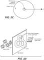
- exemplary color array panel 100suffers from a "yellow tail effect,” or a point spread function (PSF) that shifts colors as a function of distance from center. That is to say, light traveling a relatively long optical path, redirected back to spatial regions close to or in light sources, can be spatially spread into wide angles and areas, and cause color shifts (e.g., yellow tails) - particularly with light recycling with one or more reflections.
- PSFpoint spread function
- FIGS. 2A, 2B and 2Cshow the yellow tail effect.
- FIG. 2Dillustrates an example PSF having a spatially varying color shift for backlight of blue LEDs.
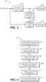
- FIG. 3illustrates an exemplary configuration of display logic in a display system 300.
- the display system 300includes backlight control logic 302 to control illumination sources in backlight 304. These illumination sources may be same or similar to illumination sources 104 shown in FIG. 1 .
- Backlight control logic 302can be operatively coupled with an image data source (not shown) (e.g., a set-top box, networked server, storage media or the like) and is configured to receive image data from the image data source.
- Image frames received or generated from image data from an internal or external sourcemay be used by the backlight control logic 302 to drive the backlight 304.
- backlight control logic 302may be configured to control backlight 304 to illuminate one or more pixels or sub-pixels with a specific intensity.
- the image framesmay be used by the backlight control logic 302 to derive individual or aggregate drive values in various frames in various resolutions.
- backlight control logic 302is logically coupled to light field simulation logic 306.
- Light field simulation logic 306computes one or more influences on the light field, including the yellow tail effect, and, optionally, illumination source binning, temperature dependence on system components and the like. Based on these influences, light field simulation logic 306 and/or modulator control logic 308 (e.g., LCD panel control logic) can mitigate them for improved picture quality. For example, to mitigate the yellow tail effect, drive values to the modulator 310 (e.g., an LCD panel) can be biased to be more blue.
- a light field simulationcan utilize nine convolution channels representing three color tristimulus values for each of the three primary colors.
- the light field simulationmodels the individually controllable illumination sources of the backlight as having a first PSF for broadband light spectral components and a second PSF for yellow light spectral components - or two convolution channels, not nine.
- the first PSFis narrower than the overlapping second PSF from the yellow tail effect.
- Light field simulation logic 306can include a convolution channel to compensate for binning (lack or insufficiency thereof) of backlight LEDs (e.g., illumination sources 102).
- backlight LEDse.g., illumination sources 102
- white LEDsconstructed with blue LED dies and yellow phosphor (e.g., YAG phosphor)
- yellow phosphore.g., YAG phosphor
- binning variation of white LEDs with wide performance rangescan reduce display accuracy and uniformity.
- the yellow phosphor material on each blue LED diecan vary causing a differing white point.
- the yellow phosphor on each blue LED diecan also have varying spectral emission.
- these UV or blue LEDscan have different intensity for constant power or vary in emission spectrums.
- light field simulation logic 306can be used to compensate for temperature dependence of display performance with additional convolution channels.
- derating function(s)can be used to account, either individually or collectively, for temperature dependence of illumination sources or a conversion layer.
- a temperature dependent point spread functioncan be used to address optical sheet warping.
- one or more temperature measurementscan be taken from one or more sensors (disposed within the optical stack) or temperature can be inferred by a display characteristic (e.g., performance change over time).
- FIG. 4illustrates an exemplary flow diagram 400 for driving a local dimming display.
- drive signals for the backlighte.g., illumination sources 104
- the driven backlightproduces a first light, in step 404.
- the first lightcan be a broadband light (e.g., white light), UV spectral components, blue spectral components, or any portion of the spectrum.
- first lightis converted into a second light.
- a conversion layerreceives the first light produces second light with desired colors (e.g., red or green light).
- step 408drive values for a modulator (e.g., an LCD panel), preferably a subpixel modulator for each primary color, are generated based on input image data.
- the results of the one or more light field simulationsare used to adjust, modify or weigh modulator drive values, as reflected in step 412.
- One or more light field simulations for compensationare performed in step 410.
- light field simulationscan address, as examples, (i) color shifts as a function of a backlight point spread function, (ii) a difference between a performance characteristic of an illumination source of the one or more illumination sources of the backlight and a performance characteristic of the backlight, (iii) temperature variance on performance, or (iv) combinations thereof.
- flow diagram 400 described hereinis for illustrative purposes only and that various modifications or changes in light thereof will be suggested to persons skilled in the art.
- the steps noted in flow diagram 400may occur out of the order noted in FIG. 4 , may include additional steps, and/or may omit some steps altogether.
- steps 402 and 408may in fact be executed substantially concurrently or in reverse order.
- step 410can be performed before step 404. All such modifications and variations are intended to be included within the scope of this disclosure.
- Embodimentsinclude an apparatus comprising a processor and configured to perform any one of the foregoing methods as discussed above.
- Embodimentsinclude a computer readable storage medium, comprising software instructions, which when executed by one or more processors causes performance of any one of the foregoing methods as discussed above.
- the techniques described hereinare implemented by one or more special-purpose computing devices.
- the special-purpose computing devicesmay be hard-wired to perform the techniques, or may include digital electronic devices such as one or more application-specific integrated circuits (ASICs) or field programmable gate arrays (FPGAs) that are persistently programmed to perform the techniques, or may include one or more general purpose hardware processors programmed to perform the techniques pursuant to program instructions in firmware, memory, other storage, or a combination.
- ASICsapplication-specific integrated circuits
- FPGAsfield programmable gate arrays
- Such special-purpose computing devicesmay also combine custom hard-wired logic, ASICs, or FPGAs with custom programming to accomplish the techniques.
- the special-purpose computing devicesmay be desktop computer systems, portable computer systems, handheld devices, networking devices or any other device that incorporates hard-wired and/or program logic to implement the techniques.
- FIG. 5is a block diagram that illustrates a computer system 500 upon which an embodiment of the invention may be implemented.
- Computer system 500includes a bus 502 or other communication mechanism for communicating information, and a hardware processor 504 coupled with bus 502 for processing information.
- Hardware processor 504may be, for example, a general purpose microprocessor.
- Computer system 500also includes a main memory 506, such as a random access memory (RAM) or other dynamic storage device, coupled to bus 502 for storing information and instructions to be executed by processor 504.
- Main memory 506also may be used for storing temporary variables or other intermediate information during execution of instructions to be executed by processor 504.
- Such instructionswhen stored in storage media accessible to processor 504, render computer system 500 into a special-purpose machine that is customized to perform the operations specified in the instructions.
- Computer system 500further includes a read only memory (ROM) 508 or other static storage device coupled to bus 502 for storing static information and instructions for processor 504.
- ROMread only memory
- a storage device 510such as a magnetic disk or optical disk, is provided and coupled to bus 502 for storing information and instructions.
- Computer system 500may be coupled via bus 502 to a display 512, such as a liquid crystal display (LCD), for displaying information to a computer user.
- a display 512such as a liquid crystal display (LCD)
- An input device 514is coupled to bus 502 for communicating information and command selections to processor 504.
- cursor control 516is Another type of user input device
- cursor control 516such as a mouse, a trackball, or cursor direction keys for communicating direction information and command selections to processor 504 and for controlling cursor movement on display 512.
- This input devicetypically has two degrees of freedom in two axes, a first axis (e.g., x) and a second axis (e.g., y), that allows the device to specify positions in a plane.
- Computer system 500may implement the techniques described herein using customized hard-wired logic, one or more ASICs or FPGAs, firmware and/or program logic which in combination with the computer system causes or programs computer system 500 to be a special-purpose machine. According to one embodiment, the techniques herein are performed by computer system 500 in response to processor 504 executing one or more sequences of one or more instructions contained in main memory 506. Such instructions may be read into main memory 506 from another storage medium, such as storage device 510. Execution of the sequences of instructions contained in main memory 506 causes processor 504 to perform the process steps described herein. In alternative embodiments, hard-wired circuitry may be used in place of or in combination with software instructions.
- Non-volatile mediaincludes, for example, optical or magnetic disks, such as storage device 510.
- Volatile mediaincludes dynamic memory, such as main memory 506.
- Common forms of storage mediainclude, for example, a floppy disk, a flexible disk, hard disk, solid state drive, magnetic tape, or any other magnetic data storage medium, a CD-ROM, any other optical data storage medium, any physical medium with patterns of holes, a RAM, a PROM, and EPROM, a FLASH-EPROM, NVRAM, any other memory chip or cartridge.
- Storage mediais distinct from but may be used in conjunction with transmission media.
- Transmission mediaparticipates in transferring information between storage media.
- transmission mediaincludes coaxial cables, copper wire and fiber optics, including the wires that comprise bus 502.
- transmission mediacan also take the form of acoustic or light waves, such as those generated during radio-wave and infra-red data communications.
- Various forms of mediamay be involved in carrying one or more sequences of one or more instructions to processor 504 for execution.
- the instructionsmay initially be carried on a magnetic disk or solid state drive of a remote computer.
- the remote computercan load the instructions into its dynamic memory and send the instructions over a telephone line using a modem.
- a modem local to computer system 500can receive the data on the telephone line and use an infra-red transmitter to convert the data to an infra-red signal.
- An infra-red detectorcan receive the data carried in the infra-red signal and appropriate circuitry can place the data on bus 502.
- Bus 502carries the data to main memory 506, from which processor 504 retrieves and executes the instructions.
- the instructions received by main memory 506may optionally be stored on storage device 510 either before or after execution by processor 504.
- Computer system 500also includes a communication interface 518 coupled to bus 502.
- Communication interface 518provides a two-way data communication coupling to a network link 520 that is connected to a local network 522.
- communication interface 518may be an integrated services digital network (ISDN) card, cable modem, satellite modem, or a modem to provide a data communication connection to a corresponding type of telephone line.
- ISDNintegrated services digital network
- communication interface 518may be a local area network (LAN) card to provide a data communication connection to a compatible LAN.
- LANlocal area network
- Wireless linksmay also be implemented.
- communication interface 518sends and receives electrical, electromagnetic or optical signals that carry digital data streams representing various types of information.
- Network link 520typically provides data communication through one or more networks to other data devices.
- network link 520may provide a connection through local network 522 to a host computer 524 or to data equipment operated by an Internet Service Provider (ISP) 526.
- ISP 526in turn provides data communication services through the world wide packet data communication network now commonly referred to as the "Internet" 528.
- Internet 528uses electrical, electromagnetic or optical signals that carry digital data streams.
- the signals through the various networks and the signals on network link 520 and through communication interface 518, which carry the digital data to and from computer system 500,are example forms of transmission media.
- Computer system 500can send messages and receive data, including program code, through the network(s), network link 520 and communication interface 518.
- a server 530might transmit a requested code for an application program through Internet 528, ISP 526, local network 522 and communication interface 518.
- the received codemay be executed by processor 504 as it is received, and/or stored in storage device 510, or other non-volatile storage for later execution.
- Figure 6Aillustrates a simplified configuration for local dimming with light conversion.
- Figure 6Billustrates a simplified configuration for local dimming with light conversion with compensation for spatial color non-uniformity.
- techniques for QD local dimmingmitigates a variance in color point spread function (PSF) across the screen. This can be done mathematically accurately by creating multiple light field simulations to change the parameters on an LCD solving matrix.
- PSFcolor point spread function
- a typical implementationcan use nine light field simulations; however, for consumer applications, a perfect mathematical solution is generally not needed.
- logic 608determines one or more drive signals controlling backlight illumination sources. Based on these drive signals backlight illumination sources (e.g., LEDs, LED 210) emit first light (e.g., broad spectrum white light, blue light, ultraviolet light) onto one or more light conversion layers (e.g., quantum dot layers, QD sheet 212, or the like).
- backlight illumination sourcese.g., LEDs, LED 210
- first lighte.g., broad spectrum white light, blue light, ultraviolet light
- light conversion layerse.g., quantum dot layers, QD sheet 212, or the like.
- a backlight algorithm for light field simulation 610where the PSF is assumed to result in a uniform white light, defines a first path 612 for intermediate LCD drive values.
- An additional pathcorrects for variations from a white, uniform solution to reduce spatial color non-uniformity.
- compensation logic 614can spatially scale the red, green, and blue primaries, in the case of an RGB system.
- compensation logic 614can be accomplished by a suitable lookup table (LUT), e.g., a one dimensional, two dimensional, or three dimensional LUT. Compensation can be determined for one or more color components.
- LUTlookup table
Landscapes
- Physics & Mathematics (AREA)
- Engineering & Computer Science (AREA)
- General Physics & Mathematics (AREA)
- Computer Hardware Design (AREA)
- Theoretical Computer Science (AREA)
- Nonlinear Science (AREA)
- Chemical & Material Sciences (AREA)
- Crystallography & Structural Chemistry (AREA)
- Mathematical Physics (AREA)
- Optics & Photonics (AREA)
- Control Of Indicators Other Than Cathode Ray Tubes (AREA)
- Liquid Crystal Display Device Control (AREA)
- Liquid Crystal (AREA)
- Control Of El Displays (AREA)
- Devices For Indicating Variable Information By Combining Individual Elements (AREA)
- Planar Illumination Modules (AREA)
- Led Device Packages (AREA)
Description
- This application claims the benefit of priority to
United States Provisional Patent Application No. 62/040,352 filed 21 August 2014 - This application is a European divisional application of Euro-PCT patent application
EP 15833257.7 (reference: D14100EP01), filed 20 August 2015 - The present invention relates to a display device, a method of driving a display device, and a computer readable storage medium.
- Color filter arrays in liquid crystal displays (LCDs) and organic light-emitting diode (OLED) displays are commonly produced by photolithographic techniques, or printing techniques, as part of the LCD and OLED panel production process. Color filters in emissive displays such as LCD and OLED displays typically consist of red, green and blue filters. The color filters are patterned over the pixel array to allow the pixel elements to modulate the emitted light by color, as well as by intensity. In operation, a broadband light source (e.g., white light) provides light to pixel elements, for example, in LCD display systems. Alternatively, broadband light is created by white OLED pixel elements in OLED display systems. A pixel element can vary the intensity of the broadband light transmitting out of the pixel element. The intensity modulated broadband light of each pixel element can be further color filtered by overlaying color filters. Considerable light is wasted by color filters because, for example, in order to produce red light spectrum (e.g., about 620-740 nanometers), then green light (e.g., about 520-570 nanometers) spectrum and blue light spectrum (e.g., about 450-495 nanometers) of the broadband light source would be blocked. Additionally, this wasted light is converted into harmful heat which degrades the performance and lifetime of the display system.
- Thus, engineering a display system with wide color gamut and high luminance has been recognized as a costly endeavor by many display manufactures. Because of a high number of relatively expensive optical, audio, electronic and mechanical components involved and the complexity in integrating all of them into a single system, the cost of manufacturing a praiseworthy display system is typically very high.
- Accordingly, it is seen by the inventors here that a dual modulation display with light conversion can provide many performance benefits over conventional techniques employing color filters. Additionally, as discovered by the inventors, introduction of light conversion to a local dimming display architecture results in color non-uniformity color. Techniques to compensate for color non-uniformity, particularly for a white light local dimming display, are provided.
- The approaches described in this section are approaches that could be pursued, but not necessarily approaches that have been previously conceived or pursued. Therefore, unless otherwise indicated, it should not be assumed that any of the approaches described in this section qualify as prior art merely by virtue of their inclusion in this section. Similarly, issues identified with respect to one or more approaches should not assume to have been recognized in any prior art on the basis of this section, unless otherwise indicated.
- Document
WO 2014/137565 A1 , which has been published after the priority dale of the present application describes techniques for driving a dual modulation display including generating backlight drive signal to drive individually controllable illumination sources. - Document
WO 2014/025677 A1 relates to display systems, and in particular, to light sources in display systems that comprise two or more levels of light modulations. - Document
US 2009/322800 A1 describes an HDR display including a backlight with an array of blue LEDs and a yellow phosphor coating for converting a portion of the blue light emitted by the LEDs in yellow light that stimulates both the red and green receptors of the eye. A global color compensation is replied by adjusting, LCD values to shift the global white point to the desired color. - Document
WO 2013/188298 A2 describes a dual modulator display system and a method for rendering target image data upon the dual modulator display system. The display system receives target image data, possible HDR image data and first calculates display control signals and then calculates backlight control signal from the display control signal. - The present invention is set out in the appended claims. In an embodiment of the present invention, driving a dual modulation display includes generating backlight drive signals for individually-controllable illumination sources. The illumination sources emit first light, such as ultraviolet or blue light, onto a light conversion layer. The light conversion layer converts the first light into second light, such as white light. The light conversion layer can include quantum dot materials. Intermediate liquid crystal display (LCD) modulation drive signals are determined based on one or more light field simulations, which assumes little or no spatial color shift. These intermediate LCD modulation drive signals can be adjusted based on one or more color field simulations to account for non-uniform, spatial color shifts resulting from using the light conversion layer.
- The present invention is illustrated by way of example, and not by way of limitation, in the figures of the accompanying drawings and in which like reference numerals refer to similar elements and in which:
FIG. 1 illustrates an exemplary color array panel comprising a conversion layer;FIGS. 2A, 2B and2C illustrate an example PSF having a color shift as a function of distance from center.FIG. 2D illustrates an example PSF having a spatially varying color shift for backlight of blue LEDs.FIG. 3 illustrates an exemplary configuration of display logic in a display system;FIG. 4 illustrates an exemplary flow diagram for driving a local dimming display; andFIG. 5 illustrates an example hardware platform on which a computer or a computing device as described herein may be implemented, according a possible embodiment of the present invention.FIGS. 6A and 6B illustrate simplified configurations of local dimming with light conversion.- The following description and drawings are illustrative of the invention and are not to be construed as limiting the invention. Numerous specific details are described to provide a thorough understanding of the invention. However, in certain instances, well known or conventional details are not described in order to avoid obscuring the description of the invention. Additionally, details from
US Patent Application 14/370,115 , entitled "Techniques for Dual Modulation Display with Light Conversion,". FIG. 1 illustrates an exemplarycolor array panel 100 comprising anoptical stack 101.Optical stack 101 can include, without limitation:- i.
conversion layer 102; - ii.
illumination sources 104; - iii.
reflector surface 106; - iv.
diffuser layer 108; - v.
light recycling film 110; and - vi.
light modulation layer 112. Conversion layer 102, disposed in front (from a viewer's perspective) ofillumination sources 104, can comprise quantum dot or phosphor materials. Quantum dot (e.g., nano-scale particles using a quantum confinement effect for light emission) or phosphor materials can be coated, attached to, doped, or otherwise disposed on a top surface, bottom surface, or both surfaces of an optical layer to formconversion layer 102. Quantum dot or phosphor materials may also be embedded within the optical layer. These materials may be disposed with the optical layer in any combination or order of various disposition methods.Conversion layer 102, using quantum dot color arrays or phosphor color arrays, impart colors in a color display system. A red quantum dot or phosphor material absorbs light of higher energies or shorter wavelengths such as green and blue light and emits red light. A green quantum dot or phosphor material absorbs blue light and emit green light. Accordingly, as an embodiment of the present invention,conversion layer 102 produces desired colors: red and green light converted from a blue light source; while blue light is emitted from the blue light source directly.- In an embodiment,
conversion layer 102 is a single sheet (or, alternatively, multiple of segments arranged to form a single plane) extending, in width and height, to be substantially equal to dimensions of an active area of the display device. For example,conversion layer 102 can measure, diagonally, about 4 inches, 10 inches, 32 inches, 40 inches, 50 inches, 58 inches or more. Additionally,conversion layer 102 can have an aspect ratio, or the proportional relationship between width and height, of 16:9, 4:3, 3:2, 5:3, 5:4, or 1:1, among others. As illustrated inFIG. 1 ,conversion layer 102 is disposed away fromillumination source 104. In an alternative embodiment of the present invention,conversion layer 102 comprises a plurality of segments. In a specific embodiment, each segment of the plurality of segments is associated with asingle illumination source 104. Illumination sources 104 can be any source of electromagnetic energy useable byconversion layer 102 to produce perceptible light for human or machine vision. For example,illumination sources 104 can include one or more of OLED, RGB LED, broadband LED, blue spectrum LED, ultraviolet spectrum LED, or the like.- These
illumination sources 104 can be arranged as an array extending substantially the length and height of the active area of the display device. The pitch density betweenillumination sources 104 can equal or correspond to the pixel resolution of the display. That is to say, the ratio ofillumination sources 104 to the number of pixel can be 1:1 (e.g., 1920 × 1080, 3840 × 2160, or 7680 × 4320 illumination sources for respective display resolution). In this case, the position of each of theillumination sources 104 can be directly aligned behind (from viewer's perspective) a corresponding pixel. In other cases,illuminations sources 104 can be disposed with a lateral offset from a corresponding pixel or between two pixels. The pitch betweenilluminations sources 104 can be uniform or non-uniform, for example, pitch density can be higher in proximity to a central active area of display than in a periphery, edges, corners, or black borders in letterbox format. - In other embodiments, the ratio between of
illumination sources 104 to the number of pixel can be lower, such as 1:2, 1:3, 1:4, 1:10, or more. In this case, the resolution of the backlight image will be decreased. Alternatively, the ratio can be higher, such as 2:1, 3:1, or less. For example, an illumination source can be associated with a subpixel, instead of a pixel or group of pixels. - These
illumination sources 104 are individually controlled or, alternatively, a subset of them can be collectively controlled in unison. The flexibility of backlight control through individuallycontrollable illumination sources 104 permits local dimming. Additional details about local dimming can be found inU.S. Patent No. 8,277,056 , entitled "Locally Dimmed Display,". However, despite individual control ofillumination sources 104, the PSF for each ofillumination sources 104 can overlap to contribute to the intensity of a plurality of pixels. - Although
FIG. 1 illustrates a direct-lit backlight display, an edge-lit display can also enjoy the benefits of the inventions taught in this disclosure (e.g., compensation for color shift from PSF and, optionally, illumination source binning or temperature variance). In such an embodiment, a spatial light modulator illuminated by one or more light sources positioned at an edge of the spatial light modulator. Additional details about edge-lit, local dimming can be found inU.S. Patent No. 8,172,401 , entitled "Edge Lit Locally Dimmed Display,". Reflector surface 106 can be a broadband mirror surface, dichroic mirror surface reflecting a predetermined spectrum (e.g., one or more primary colors). Further,reflector surface 106 can include through-holes forillumination sources 104. These through-holes can be reamed, drilled, or milled.Reflector surface 106 redirects light back through theoptical stack 101 for increased efficiency.- In
FIG. 1 ,diffuser layer 108 scatters outgoing light through a range of directions so that a viewer located on an opposite side ofdiffuser 108 perceives light to originate from an increased area. In general,diffuser 108 can scatter light to a different angular extent in the horizontal and vertical planes. Light recycling film 110 is used to boost the optical efficiency of backlighting. In some embodiments, aslight modulation layer 112 can only (or substantially only) pass polarized light and that the backlight essentially produces unpolarized light. A reflective polarizer (e.g., 3M DBEF) can be used as the last optical layer beforelight modulation layer 112. Light of the wrong polarization incident on thelight modulation layer 112, which would otherwise be absorbed, is reflected back by thelight recycling film 110 towards the backlight. The reflected light would be scattered indiffuser layer 108 which randomizes the polarization. The reflected light having randomized polarization, which has a fraction of the correct polarization to pass through thelight modulation layer 112, can be redirected toward thelight modulation layer 112 as it scatters and bounces in the optical stack.- Another
light recycling film 110 can be a prismatic structured film (e.g., 3M BEF) which is used to control the direction of light exiting the backlight unit. To maximize the intensity of light within the viewing angle oflight modulation layer 112, light outside of the viewing angle can be reflected back into the optical cavity which after scattering and reflection can result in a fraction of the reflected light having the desired exiting angle within viewing angle. Light modulation layer 112 may comprise, for example, (i) an LCD panel, which is an example of a transmission-type light modulator, (ii) a deformable mirror device (DMD), which is an example of a reflection-type light modulator, or (iii) a micro-electro-mechanical system (MEMS) based modulator. The elements oflight modulator 112 are controlled according to data which defines an image being displayed.- It should be appreciated that
FIG. 1 illustrates an embodiment ofoptical stack 101, and the arrangement of elements therein can vary or can include additional elements not described. For example,light recycling film 110 can be disposed behinddiffuser layer 108, rather than in front of it. As yet another example,conversion layer 102 can be disposed anywhere withinoptical stack 101 after illumination sources 104. All such modifications and variations are intended to be included within the scope of this disclosure. - As appreciated by the inventors here, exemplary
color array panel 100 suffers from a "yellow tail effect," or a point spread function (PSF) that shifts colors as a function of distance from center. That is to say, light traveling a relatively long optical path, redirected back to spatial regions close to or in light sources, can be spatially spread into wide angles and areas, and cause color shifts (e.g., yellow tails) - particularly with light recycling with one or more reflections. In such a system, for example, the light in the center of a point spread function of a direct-lit light emitter would be mostly converted, but rejected light components can bounce back in and convert with less green and red as the distance from the center of the point spread function of the light emitter to outer circumferences increases, giving rise to a color shift to the point spread function (PSF). The PSF tail becomes increasingly yellow even when the PSF center has a desired white point. Without the presence of compensation, color shift degradation may be especially noticeable or even visually prominent.FIGS. 2A, 2B and2C , as simple illustrations, show the yellow tail effect.FIG. 2D illustrates an example PSF having a spatially varying color shift for backlight of blue LEDs. FIG. 3 illustrates an exemplary configuration of display logic in adisplay system 300. Thedisplay system 300 includesbacklight control logic 302 to control illumination sources inbacklight 304. These illumination sources may be same or similar toillumination sources 104 shown inFIG. 1 .Backlight control logic 302 can be operatively coupled with an image data source (not shown) (e.g., a set-top box, networked server, storage media or the like) and is configured to receive image data from the image data source. Image frames received or generated from image data from an internal or external source may be used by thebacklight control logic 302 to drive thebacklight 304. For example,backlight control logic 302 may be configured to controlbacklight 304 to illuminate one or more pixels or sub-pixels with a specific intensity. The image frames may be used by thebacklight control logic 302 to derive individual or aggregate drive values in various frames in various resolutions.- In this embodiment,
backlight control logic 302 is logically coupled to lightfield simulation logic 306. Lightfield simulation logic 306 computes one or more influences on the light field, including the yellow tail effect, and, optionally, illumination source binning, temperature dependence on system components and the like. Based on these influences, lightfield simulation logic 306 and/or modulator control logic 308 (e.g., LCD panel control logic) can mitigate them for improved picture quality. For example, to mitigate the yellow tail effect, drive values to the modulator 310 (e.g., an LCD panel) can be biased to be more blue. - In one example not part of the present invention, a light field simulation can utilize nine convolution channels representing three color tristimulus values for each of the three primary colors. However, this is computationally expensive. In the present invention, the light field simulation models the individually controllable illumination sources of the backlight as having a first PSF for broadband light spectral components and a second PSF for yellow light spectral components - or two convolution channels, not nine. The first PSF is narrower than the overlapping second PSF from the yellow tail effect.
- Light
field simulation logic 306 can include a convolution channel to compensate for binning (lack or insufficiency thereof) of backlight LEDs (e.g., illumination sources 102). For a broadband backlight, white LEDs, constructed with blue LED dies and yellow phosphor (e.g., YAG phosphor), can be used. However, binning variation of white LEDs with wide performance ranges can reduce display accuracy and uniformity. In particular, the yellow phosphor material on each blue LED die can vary causing a differing white point. The yellow phosphor on each blue LED die can also have varying spectral emission. Similarly, in an embodiment exclusively using UV and/or blue spectral components for backlighting, these UV or blue LEDs can have different intensity for constant power or vary in emission spectrums. - In an example, light
field simulation logic 306 can be used to compensate for temperature dependence of display performance with additional convolution channels. For example, derating function(s) can be used to account, either individually or collectively, for temperature dependence of illumination sources or a conversion layer. As another example, a temperature dependent point spread function can be used to address optical sheet warping. In an example, one or more temperature measurements can be taken from one or more sensors (disposed within the optical stack) or temperature can be inferred by a display characteristic (e.g., performance change over time). FIG. 4 illustrates an exemplary flow diagram 400 for driving a local dimming display. Instep 402, drive signals for the backlight (e.g., illumination sources 104) can be generated. The driven backlight produces a first light, instep 404. The first light can be a broadband light (e.g., white light), UV spectral components, blue spectral components, or any portion of the spectrum. As shown instep 406, first light is converted into a second light. For example, a conversion layer receives the first light produces second light with desired colors (e.g., red or green light).- Next, in
step 408, drive values for a modulator (e.g., an LCD panel), preferably a subpixel modulator for each primary color, are generated based on input image data. The results of the one or more light field simulations are used to adjust, modify or weigh modulator drive values, as reflected in step 412. One or more light field simulations for compensation are performed instep 410. As described herein, light field simulations can address, as examples, (i) color shifts as a function of a backlight point spread function, (ii) a difference between a performance characteristic of an illumination source of the one or more illumination sources of the backlight and a performance characteristic of the backlight, (iii) temperature variance on performance, or (iv) combinations thereof. - It is appreciated that flow diagram 400 described herein is for illustrative purposes only and that various modifications or changes in light thereof will be suggested to persons skilled in the art. In alternative implementations not part of the claimed invention, the steps noted in flow diagram 400 may occur out of the order noted in
FIG. 4 , may include additional steps, and/or may omit some steps altogether. For example, steps 402 and 408 may in fact be executed substantially concurrently or in reverse order. As another example, step 410 can be performed beforestep 404. All such modifications and variations are intended to be included within the scope of this disclosure. - Embodiments include an apparatus comprising a processor and configured to perform any one of the foregoing methods as discussed above.
- Embodiments include a computer readable storage medium, comprising software instructions, which when executed by one or more processors causes performance of any one of the foregoing methods as discussed above.
- According to one embodiment, the techniques described herein are implemented by one or more special-purpose computing devices. The special-purpose computing devices may be hard-wired to perform the techniques, or may include digital electronic devices such as one or more application-specific integrated circuits (ASICs) or field programmable gate arrays (FPGAs) that are persistently programmed to perform the techniques, or may include one or more general purpose hardware processors programmed to perform the techniques pursuant to program instructions in firmware, memory, other storage, or a combination. Such special-purpose computing devices may also combine custom hard-wired logic, ASICs, or FPGAs with custom programming to accomplish the techniques. The special-purpose computing devices may be desktop computer systems, portable computer systems, handheld devices, networking devices or any other device that incorporates hard-wired and/or program logic to implement the techniques.
- For example,
FIG. 5 is a block diagram that illustrates acomputer system 500 upon which an embodiment of the invention may be implemented.Computer system 500 includes abus 502 or other communication mechanism for communicating information, and ahardware processor 504 coupled withbus 502 for processing information.Hardware processor 504 may be, for example, a general purpose microprocessor. Computer system 500 also includes amain memory 506, such as a random access memory (RAM) or other dynamic storage device, coupled tobus 502 for storing information and instructions to be executed byprocessor 504.Main memory 506 also may be used for storing temporary variables or other intermediate information during execution of instructions to be executed byprocessor 504. Such instructions, when stored in storage media accessible toprocessor 504, rendercomputer system 500 into a special-purpose machine that is customized to perform the operations specified in the instructions.Computer system 500 further includes a read only memory (ROM) 508 or other static storage device coupled tobus 502 for storing static information and instructions forprocessor 504. Astorage device 510, such as a magnetic disk or optical disk, is provided and coupled tobus 502 for storing information and instructions.Computer system 500 may be coupled viabus 502 to adisplay 512, such as a liquid crystal display (LCD), for displaying information to a computer user. Aninput device 514, including alphanumeric and other keys, is coupled tobus 502 for communicating information and command selections toprocessor 504. Another type of user input device iscursor control 516, such as a mouse, a trackball, or cursor direction keys for communicating direction information and command selections toprocessor 504 and for controlling cursor movement ondisplay 512. This input device typically has two degrees of freedom in two axes, a first axis (e.g., x) and a second axis (e.g., y), that allows the device to specify positions in a plane.Computer system 500 may implement the techniques described herein using customized hard-wired logic, one or more ASICs or FPGAs, firmware and/or program logic which in combination with the computer system causes orprograms computer system 500 to be a special-purpose machine. According to one embodiment, the techniques herein are performed bycomputer system 500 in response toprocessor 504 executing one or more sequences of one or more instructions contained inmain memory 506. Such instructions may be read intomain memory 506 from another storage medium, such asstorage device 510. Execution of the sequences of instructions contained inmain memory 506 causesprocessor 504 to perform the process steps described herein. In alternative embodiments, hard-wired circuitry may be used in place of or in combination with software instructions.- The term "storage media" as used herein refers to any media that store data and/or instructions that cause a machine to operation in a specific fashion. Such storage media may comprise non-volatile media and/or volatile media. Non-volatile media includes, for example, optical or magnetic disks, such as
storage device 510. Volatile media includes dynamic memory, such asmain memory 506. Common forms of storage media include, for example, a floppy disk, a flexible disk, hard disk, solid state drive, magnetic tape, or any other magnetic data storage medium, a CD-ROM, any other optical data storage medium, any physical medium with patterns of holes, a RAM, a PROM, and EPROM, a FLASH-EPROM, NVRAM, any other memory chip or cartridge. - Storage media is distinct from but may be used in conjunction with transmission media. Transmission media participates in transferring information between storage media. For example, transmission media includes coaxial cables, copper wire and fiber optics, including the wires that comprise
bus 502. Transmission media can also take the form of acoustic or light waves, such as those generated during radio-wave and infra-red data communications. - Various forms of media may be involved in carrying one or more sequences of one or more instructions to
processor 504 for execution. For example, the instructions may initially be carried on a magnetic disk or solid state drive of a remote computer. The remote computer can load the instructions into its dynamic memory and send the instructions over a telephone line using a modem. A modem local tocomputer system 500 can receive the data on the telephone line and use an infra-red transmitter to convert the data to an infra-red signal. An infra-red detector can receive the data carried in the infra-red signal and appropriate circuitry can place the data onbus 502.Bus 502 carries the data tomain memory 506, from whichprocessor 504 retrieves and executes the instructions. The instructions received bymain memory 506 may optionally be stored onstorage device 510 either before or after execution byprocessor 504. Computer system 500 also includes acommunication interface 518 coupled tobus 502.Communication interface 518 provides a two-way data communication coupling to anetwork link 520 that is connected to alocal network 522. For example,communication interface 518 may be an integrated services digital network (ISDN) card, cable modem, satellite modem, or a modem to provide a data communication connection to a corresponding type of telephone line. As another example,communication interface 518 may be a local area network (LAN) card to provide a data communication connection to a compatible LAN. Wireless links may also be implemented. In any such implementation,communication interface 518 sends and receives electrical, electromagnetic or optical signals that carry digital data streams representing various types of information.- Network link 520 typically provides data communication through one or more networks to other data devices. For example,
network link 520 may provide a connection throughlocal network 522 to ahost computer 524 or to data equipment operated by an Internet Service Provider (ISP) 526.ISP 526 in turn provides data communication services through the world wide packet data communication network now commonly referred to as the "Internet" 528.Local network 522 andInternet 528 both use electrical, electromagnetic or optical signals that carry digital data streams. The signals through the various networks and the signals onnetwork link 520 and throughcommunication interface 518, which carry the digital data to and fromcomputer system 500, are example forms of transmission media. Computer system 500 can send messages and receive data, including program code, through the network(s),network link 520 andcommunication interface 518. In the Internet example, aserver 530 might transmit a requested code for an application program throughInternet 528,ISP 526,local network 522 andcommunication interface 518. The received code may be executed byprocessor 504 as it is received, and/or stored instorage device 510, or other non-volatile storage for later execution.Figure 6A illustrates a simplified configuration for local dimming with light conversion.Figure 6B illustrates a simplified configuration for local dimming with light conversion with compensation for spatial color non-uniformity.- In an example, techniques for QD local dimming mitigates a variance in color point spread function (PSF) across the screen. This can be done mathematically accurately by creating multiple light field simulations to change the parameters on an LCD solving matrix. A typical implementation can use nine light field simulations; however, for consumer applications, a perfect mathematical solution is generally not needed.
- As an example,
logic 608 determines one or more drive signals controlling backlight illumination sources. Based on these drive signals backlight illumination sources (e.g., LEDs, LED 210) emit first light (e.g., broad spectrum white light, blue light, ultraviolet light) onto one or more light conversion layers (e.g., quantum dot layers,QD sheet 212, or the like). - Based on the teachings herein, a backlight algorithm for
light field simulation 610, where the PSF is assumed to result in a uniform white light, defines afirst path 612 for intermediate LCD drive values. An additional path corrects for variations from a white, uniform solution to reduce spatial color non-uniformity. - As a further example, instead of corrections to the matrix, compensation logic 614 can spatially scale the red, green, and blue primaries, in the case of an RGB system. Alternatively to scaling, compensation logic 614 can be accomplished by a suitable lookup table (LUT), e.g., a one dimensional, two dimensional, or three dimensional LUT. Compensation can be determined for one or more color components.
- In the foregoing specification, possible embodiments of the invention have been described with reference to numerous specific details that may vary from implementation to implementation. Thus, the sole and exclusive indicator of what is the invention, and is intended by the applicants to be the invention, is the set of claims that issue from this application, in the specific form in which such claims issue, including any subsequent correction. Hence, no limitation, element, property, feature, advantage or attribute that is not expressly recited in a claim should limit the scope of such claim in any way. The specification and drawings are, accordingly, to be regarded in an illustrative rather than a restrictive sense. Numerous modifications and variations of the invention are possible in light of the above teachings. Any definitions expressly set forth herein for terms contained in such claims shall govern the meaning of such terms as used in the claims. It should be further understood, for clarity, thatexempli gratia (e.g.) means "for the sake of example" (not exhaustive), which differs fromid est (i.e.) or "that is."
Claims (10)
- A display device, comprising:a backlight comprising a plurality of individually controllable illumination sources,a light conversion layer (102)a backlight control logic (302) configured to control the plurality of illumination sources on the basis of image data, wherein the illumination sources of the backlight are configured to emit first light of a first frequency spectrum onto the light conversion layer (102), wherein the light conversion layer (102) is configured to be stimulated by the first light and to convert at least a portion of the first light into second light of a second frequency spectrum different from the first frequency spectrum, the second light being white light, and wherein using the light conversion layer results in spatial color shifts for yellow light spectral components;a light modulator (310) configured to modulate the second light transmitted through individual subpixels of the display device;a logic configured to compute first and second light field simulations, wherein the first light field simulation is obtained by modelling the plurality of individually controllable illumination sources with a first point spread function for white light spectral components and the second light field simulation is for compensating the spatial color shifts for yellow light spectral components and is obtained by modelling the plurality of individually controllable illumination sources with a second point spread function for yellow light spectral components, the first point spread function being narrower than the second point spread function;a controller (308) configured to determine intermediate display modulation drive values for the light modulator based on the image data and on the first light field simulation and compensate for a spatial color non-uniformity of the second light by adjusting the intermediate display modulation drive values based on the second light field simulation.
- The display device of claim 1, wherein the light conversion layer includes quantum dot materials.
- The display device of claim 2, wherein the quantum dot materials form a sheet.
- The display device of claim 3, wherein the quantum dot materials of the light conversion layer comprise a plurality of segments.
- The display device of any of the preceding claims, wherein the illumination sources comprises one or more RGB illumination sources.
- The display device of any of the preceding claims, wherein the display device is an LCD (liquid crystal display) display device.
- The display device of any of the preceding claims, wherein the one or more illumination sources (104) comprises one or more of OLED , RGB LED, broadband LED, blue spectrum LED, ultraviolet spectrum LED.
- The display device of any of the preceding claims, wherein the light modulator is an LCD modulator, a deformable mirror device, or a micro-electro-mechanical device.
- A method of driving the display device of claim 1, the method comprising:- emitting, by the plurality of individually controllable illumination sources of the backlight, first light of a first frequency spectrum onto the light conversion layer (102),- converting, by the light conversion layer, at least a portion of the first light into second light of a second frequency spectrum different from the first frequency spectrum, the second light being white light, and wherein using the light conversion layer results in spatial color shifts for yellow light spectral components;- modulating, by the light modulator, the second light transmitted through individual subpixels of the display device;- computing, by the logic, first and second light field simulations, wherein the first light field simulations is obtained by modelling the plurality of individually controllable illumination sources with a first point spread function for white light spectral components and the second light field simulation is obtained by modelling the plurality of individually controllable illumination sources with a second point spread function for yellow light spectral components, the second light field simulation being for compensating spatial color shifts for yellow light spectral components caused by the light conversion layer, the first point spread function being narrower than the second point spread function;- determining, by the controller, intermediate display modulation drive values for the light modulator based on the image data and on the first light field simulation;- compensating, by the controller, for a spatial color non-uniformity of the second light, by adjusting the intermediate display modulation drive values based on the second light field simulation.
- A computer readable storage medium, comprising software instructions, which when executed by one or more processors cause the device of claim 1 to perform the steps of the method of claim 9.
Applications Claiming Priority (3)
| Application Number | Priority Date | Filing Date | Title |
|---|---|---|---|
| US201462040352P | 2014-08-21 | 2014-08-21 | |
| EP15833257.7AEP3183726B1 (en) | 2014-08-21 | 2015-08-20 | Techniques for dual modulation with light conversion |
| PCT/US2015/046074WO2016028994A1 (en) | 2014-08-21 | 2015-08-20 | Techniques for dual modulation with light conversion |
Related Parent Applications (1)
| Application Number | Title | Priority Date | Filing Date |
|---|---|---|---|
| EP15833257.7ADivisionEP3183726B1 (en) | 2014-08-21 | 2015-08-20 | Techniques for dual modulation with light conversion |
Publications (2)
| Publication Number | Publication Date |
|---|---|
| EP3633663A1 EP3633663A1 (en) | 2020-04-08 |
| EP3633663B1true EP3633663B1 (en) | 2024-06-19 |
Family
ID=55351252
Family Applications (2)
| Application Number | Title | Priority Date | Filing Date |
|---|---|---|---|
| EP19204517.7AActiveEP3633663B1 (en) | 2014-08-21 | 2015-08-20 | Techniques for dual modulation with light conversion |
| EP15833257.7AActiveEP3183726B1 (en) | 2014-08-21 | 2015-08-20 | Techniques for dual modulation with light conversion |
Family Applications After (1)
| Application Number | Title | Priority Date | Filing Date |
|---|---|---|---|
| EP15833257.7AActiveEP3183726B1 (en) | 2014-08-21 | 2015-08-20 | Techniques for dual modulation with light conversion |
Country Status (7)
| Country | Link |
|---|---|
| US (4) | US9810944B2 (en) |
| EP (2) | EP3633663B1 (en) |
| JP (3) | JP6236188B2 (en) |
| CN (2) | CN106663408B (en) |
| ES (1) | ES2755506T3 (en) |
| PL (1) | PL3183726T3 (en) |
| WO (1) | WO2016028994A1 (en) |
Families Citing this family (9)
| Publication number | Priority date | Publication date | Assignee | Title |
|---|---|---|---|---|
| EP3633663B1 (en)* | 2014-08-21 | 2024-06-19 | Dolby Laboratories Licensing Corporation | Techniques for dual modulation with light conversion |
| US10210820B2 (en)* | 2016-02-03 | 2019-02-19 | Canon Kabushiki Kaisha | Image display apparatus and method for controlling same |
| US10600213B2 (en)* | 2016-02-27 | 2020-03-24 | Focal Sharp, Inc. | Method and apparatus for color-preserving spectrum reshape |
| US10607551B2 (en) | 2017-03-21 | 2020-03-31 | Dolby Laboratories Licesing Corporation | Temperature-compensated LED-backlit liquid crystal displays |
| US10818210B2 (en)* | 2019-01-31 | 2020-10-27 | Novatek Microelectronics Corp. | Display apparatus and brightness uniformity compensation method thereof |
| TWI725553B (en)* | 2019-09-24 | 2021-04-21 | 友達光電股份有限公司 | Display device and method of manufacturing thereof |
| CN111524489B (en)* | 2020-04-23 | 2022-08-19 | 中国科学院上海技术物理研究所 | Ultrahigh frame frequency simulation method based on composite coding |
| US20230359029A1 (en)* | 2022-05-06 | 2023-11-09 | Meta Platforms, Inc. | Tunable Florescent Quantum Dot System for Eye Tracking with Virtual Reality and Augmented Reality Applications |
| JP2024168641A (en)* | 2023-05-24 | 2024-12-05 | マクセル株式会社 | Head-up display device and vehicle |
Family Cites Families (137)
| Publication number | Priority date | Publication date | Assignee | Title |
|---|---|---|---|---|
| DE3581546D1 (en) | 1984-03-12 | 1991-03-07 | Matsushita Electric Industrial Co Ltd | OPTICAL FILTER AND PRODUCTION METHOD. |
| JPH0278393A (en) | 1988-09-14 | 1990-03-19 | Hitachi Ltd | Stereoscopic color picture display device |
| JP3187669B2 (en) | 1994-04-01 | 2001-07-11 | 日本碍子株式会社 | Display element and display device |
| US5737045A (en) | 1995-09-22 | 1998-04-07 | Ois Optical Imaging Systems, Inc. | LCD with notch filter |
| US5754159A (en) | 1995-11-20 | 1998-05-19 | Texas Instruments Incorporated | Integrated liquid crystal display and backlight system for an electronic apparatus |
| KR100286828B1 (en) | 1996-09-18 | 2001-04-16 | 니시무로 타이죠 | Flat panel display device |
| JP3787983B2 (en) | 1997-06-18 | 2006-06-21 | セイコーエプソン株式会社 | Optical switching element, image display device, and projection device |
| US6864626B1 (en) | 1998-06-03 | 2005-03-08 | The Regents Of The University Of California | Electronic displays using optically pumped luminescent semiconductor nanocrystals |
| US20050146258A1 (en) | 1999-06-02 | 2005-07-07 | Shimon Weiss | Electronic displays using optically pumped luminescent semiconductor nanocrystals |
| EP1042775A2 (en) | 1998-09-22 | 2000-10-11 | Fed Corporation | Inorganic-based color conversion matrix element for organic color display devices and method of fabrication |
| JP2000330504A (en) | 1999-05-18 | 2000-11-30 | Toshiba Corp | Video display device |
| EP1390806B1 (en) | 2001-02-27 | 2010-08-25 | Dolby Laboratories Licensing Corporation | High dynamic range display devices |
| US7015991B2 (en) | 2001-12-21 | 2006-03-21 | 3M Innovative Properties Company | Color pre-filter for single-panel projection display system |
| JP2003346530A (en) | 2002-05-23 | 2003-12-05 | Nippon Sheet Glass Co Ltd | Planar light source and image scanner |
| KR100712334B1 (en) | 2002-09-30 | 2007-05-02 | 엘지전자 주식회사 | How to adjust the brightness level of the liquid crystal display |
| JP4087681B2 (en) | 2002-10-29 | 2008-05-21 | 株式会社日立製作所 | LIGHTING DEVICE AND DISPLAY DEVICE USING THE SAME |
| CN100493280C (en) | 2002-12-26 | 2009-05-27 | 皇家飞利浦电子股份有限公司 | Color temperature correction of phosphor converted light emitting diodes |
| JP2004325647A (en) | 2003-04-23 | 2004-11-18 | Sharp Corp | Display element |
| EP1640787B1 (en) | 2003-06-20 | 2009-04-01 | Sharp Kabushiki Kaisha | Display |
| DE602004031427D1 (en) | 2003-07-22 | 2011-03-31 | Ngk Insulators Ltd | MEMBER ELEMENT AND DEVICE WITH CONTROLLER ELEMENT |
| US7052152B2 (en) | 2003-10-03 | 2006-05-30 | Philips Lumileds Lighting Company, Llc | LCD backlight using two-dimensional array LEDs |
| US7354172B2 (en) | 2004-03-15 | 2008-04-08 | Philips Solid-State Lighting Solutions, Inc. | Methods and apparatus for controlled lighting based on a reference gamut |
| US7768023B2 (en) | 2005-10-14 | 2010-08-03 | The Regents Of The University Of California | Photonic structures for efficient light extraction and conversion in multi-color light emitting devices |
| US8217970B2 (en)* | 2004-07-27 | 2012-07-10 | Dolby Laboratories Licensing Corporation | Rapid image rendering on dual-modulator displays |
| DK1779362T3 (en) | 2004-07-27 | 2016-06-27 | Dolby Laboratories Licensing Corp | Quick image reproduction on screen dual modulator |
| JP2006114909A (en) | 2004-10-14 | 2006-04-27 | Agilent Technol Inc | Flash module |
| WO2006046168A1 (en) | 2004-10-25 | 2006-05-04 | Koninklijke Philips Electronics N.V. | Display panel with a light valve layer |
| KR100735148B1 (en) | 2004-11-22 | 2007-07-03 | (주)케이디티 | Backlight unit by phosphorescent diffusion sheet |
| TWI263802B (en) | 2004-12-03 | 2006-10-11 | Innolux Display Corp | Color filter |
| KR101196509B1 (en) | 2005-04-01 | 2012-11-02 | 프리즘, 인코포레이티드 | Display systems and devices having screens with optical fluorescent materials |
| JP2006309219A (en) | 2005-04-25 | 2006-11-09 | Samsung Electronics Co Ltd | Self-luminous liquid crystal display device |
| KR101113236B1 (en) | 2005-04-26 | 2012-02-20 | 삼성전자주식회사 | Backlight unit for dynamic image and display device using same |
| JP2006309238A (en) | 2005-04-27 | 2006-11-09 | Samsung Electronics Co Ltd | Photoluminescence liquid crystal display |
| KR101110071B1 (en) | 2005-04-29 | 2012-02-24 | 삼성전자주식회사 | Photo-Luminescenct Liquid Crystal Display |
| KR101110072B1 (en) | 2005-06-02 | 2012-02-24 | 삼성전자주식회사 | Photo-Luminescenct Liquid Crystal Display |
| US8718437B2 (en) | 2006-03-07 | 2014-05-06 | Qd Vision, Inc. | Compositions, optical component, system including an optical component, devices, and other products |
| US8215815B2 (en) | 2005-06-07 | 2012-07-10 | Oree, Inc. | Illumination apparatus and methods of forming the same |
| US7513669B2 (en) | 2005-08-01 | 2009-04-07 | Avago Technologies General Ip (Singapore) Pte. Ltd. | Light source for LCD back-lit displays |
| TWI271883B (en) | 2005-08-04 | 2007-01-21 | Jung-Chieh Su | Light-emitting devices with high extraction efficiency |
| JP5419452B2 (en) | 2005-08-15 | 2014-02-19 | コーニンクレッカ フィリップス エヌ ヴェ | Light source and method for generating light of variable color and / or brightness |
| CN100517016C (en) | 2005-10-27 | 2009-07-22 | 鸿富锦精密工业(深圳)有限公司 | Light source and backlight module |
| US7486304B2 (en) | 2005-12-21 | 2009-02-03 | Nokia Corporation | Display device with dynamic color gamut |
| US7486854B2 (en) | 2006-01-24 | 2009-02-03 | Uni-Pixel Displays, Inc. | Optical microstructures for light extraction and control |
| US7486354B2 (en) | 2006-01-26 | 2009-02-03 | Hannstar Display Corp. | Backlight module of a liquid crystal display, display device, method of improving color gamut of a display device |
| WO2007114918A2 (en) | 2006-04-04 | 2007-10-11 | Microvision, Inc. | Electronic display with photoluminescent wavelength conversion |
| US20070268240A1 (en) | 2006-05-19 | 2007-11-22 | Lee Sang-Jin | Display device and method of driving the display device |
| US7880381B2 (en) | 2006-07-05 | 2011-02-01 | Avago Technologies General Ip (Singapore) Pte. Ltd. | LED with light absorbing encapsulant and related methodology |
| US20080074583A1 (en) | 2006-07-06 | 2008-03-27 | Intematix Corporation | Photo-luminescence color liquid crystal display |
| US7498534B2 (en) | 2006-08-30 | 2009-03-03 | 3M Innovative Properties Company | Keypad light guide |
| US7751663B2 (en) | 2006-09-21 | 2010-07-06 | Uni-Pixel Displays, Inc. | Backside reflection optical display |
| KR20090057114A (en) | 2006-09-27 | 2009-06-03 | 가부시끼가이샤 도시바 | Semiconductor light emitting device, backlight and display device comprising the semiconductor light emitting device |
| GB2442505A (en) | 2006-10-04 | 2008-04-09 | Sharp Kk | A display with a primary light source for illuminating a nanophosphor re-emission material |
| JP4851908B2 (en)* | 2006-10-10 | 2012-01-11 | 株式会社 日立ディスプレイズ | Liquid crystal display |
| KR101361861B1 (en) | 2006-11-08 | 2014-02-12 | 엘지디스플레이 주식회사 | Organic light emitting diodes and method of manufacturing the same |
| CN101543084A (en) | 2006-11-30 | 2009-09-23 | Nxp股份有限公司 | Device and method for processing color image data |
| JP2008145551A (en) | 2006-12-06 | 2008-06-26 | Sony Corp | Display device |
| BRPI0720017A2 (en) | 2006-12-11 | 2017-01-10 | Tir Technology Lp | A method and system for controlling one or more direct current operated light-emitting elements to generate a mixed light. |
| US20080172197A1 (en) | 2007-01-11 | 2008-07-17 | Motorola, Inc. | Single laser multi-color projection display with quantum dot screen |
| DE102007009530A1 (en) | 2007-02-27 | 2008-08-28 | Osram Opto Semiconductors Gmbh | Organic light-emitting diode for lighting purposes predominantly emitting white light mixed with colors and composite video signal conversation, comprises substrate layer structure, anode, cathode and intermediate arranged functional layer |
| EP2122695A4 (en) | 2007-03-08 | 2013-09-11 | 3M Innovative Properties Co | ARRANGEMENT OF LIGHT ELEMENTS |
| US7478922B2 (en) | 2007-03-14 | 2009-01-20 | Renaissance Lighting, Inc. | Set-point validation for color/intensity settings of light fixtures |
| US20100155749A1 (en) | 2007-03-19 | 2010-06-24 | Nanosys, Inc. | Light-emitting diode (led) devices comprising nanocrystals |
| KR101730164B1 (en) | 2007-07-18 | 2017-04-25 | 삼성전자주식회사 | Quantum dot-based light sheets useful for solid-state lighting |
| WO2009014707A2 (en) | 2007-07-23 | 2009-01-29 | Qd Vision, Inc. | Quantum dot light enhancement substrate and lighting device including same |
| TWI345671B (en) | 2007-08-10 | 2011-07-21 | Au Optronics Corp | Thin film transistor, pixel structure and liquid crystal display panel |
| US8128249B2 (en) | 2007-08-28 | 2012-03-06 | Qd Vision, Inc. | Apparatus for selectively backlighting a material |
| JP4856249B2 (en)* | 2007-09-27 | 2012-01-18 | シャープ株式会社 | Display device |
| WO2009041594A1 (en) | 2007-09-28 | 2009-04-02 | Dai Nippon Printing Co., Ltd. | Electroluminescence element |
| KR101376755B1 (en) | 2007-10-09 | 2014-03-24 | 삼성디스플레이 주식회사 | Display device |
| KR101415566B1 (en) | 2007-10-29 | 2014-07-04 | 삼성디스플레이 주식회사 | Display device |
| US7671542B2 (en) | 2007-11-07 | 2010-03-02 | Au Optronics Corporation | Color control of multi-zone LED backlight |
| KR100843341B1 (en) | 2007-12-05 | 2008-07-03 | 에스이피엔씨 주식회사 | Double heat insulation tube having a fusion layer, its manufacturing method and manufacturing apparatus |
| JP4613947B2 (en) | 2007-12-07 | 2011-01-19 | ソニー株式会社 | Illumination device, color conversion element, and display device |
| JP2009283438A (en) | 2007-12-07 | 2009-12-03 | Sony Corp | Lighting device, display device, and manufacturing method of lighting device |
| KR101460155B1 (en) | 2008-01-15 | 2014-11-10 | 삼성전자주식회사 | Backlight unit and liquid crystal display having the same |
| US8029139B2 (en) | 2008-01-29 | 2011-10-04 | Eastman Kodak Company | 2D/3D switchable color display apparatus with narrow band emitters |
| US20090194774A1 (en) | 2008-02-04 | 2009-08-06 | Kismart Corporation | Light source module with wavelength converting structure and the method of forming the same |
| US7832885B2 (en) | 2008-02-05 | 2010-11-16 | Kismart Corporation | Patterned wavelength converting structure |
| BRPI0822306A2 (en)* | 2008-02-14 | 2015-06-16 | Sharp Kk | Display device |
| TW200938913A (en) | 2008-03-13 | 2009-09-16 | Kismart Corp | A flat panel display capable of multi-sided viewings and its back light module |
| JP5430950B2 (en)* | 2008-04-01 | 2014-03-05 | ミツミ電機株式会社 | Image display device |
| JP2009251129A (en) | 2008-04-02 | 2009-10-29 | Optoelectronic Industry & Technology Development Association | Color filter for liquid crystal display device and liquid crystal display device |
| JP5369486B2 (en) | 2008-04-28 | 2013-12-18 | 豊田合成株式会社 | Light emitting device |
| EP2120448A1 (en) | 2008-05-14 | 2009-11-18 | Thomson Licensing | Method of processing of a compressed image into a gamut mapped image using spatial frequency analysis |
| US8197088B2 (en) | 2008-06-13 | 2012-06-12 | Barco, Inc. | Vertical handling apparatus for a display |
| US20090322800A1 (en)* | 2008-06-25 | 2009-12-31 | Dolby Laboratories Licensing Corporation | Method and apparatus in various embodiments for hdr implementation in display devices |
| US7988311B2 (en) | 2008-06-30 | 2011-08-02 | Bridgelux, Inc. | Light emitting device having a phosphor layer |
| US8314767B2 (en)* | 2008-08-30 | 2012-11-20 | Sharp Laboratories Of America, Inc. | Methods and systems for reducing view-angle-induced color shift |
| EP2164302A1 (en) | 2008-09-12 | 2010-03-17 | Ilford Imaging Switzerland Gmbh | Optical element and method for its production |
| US7858409B2 (en) | 2008-09-18 | 2010-12-28 | Koninklijke Philips Electronics N.V. | White point compensated LEDs for LCD displays |
| US8294848B2 (en) | 2008-10-01 | 2012-10-23 | Samsung Display Co., Ltd. | Liquid crystal display having light diffusion layer |
| JP2010092705A (en) | 2008-10-08 | 2010-04-22 | Sony Corp | Illuminating device and display device using this |
| ES2541846T3 (en)* | 2008-10-14 | 2015-07-27 | Dolby Laboratories Licensing Corporation | Backlight simulation at reduced resolutions to determine spatial light modulation for high dynamic range images |
| TWI416454B (en) | 2008-10-31 | 2013-11-21 | Dynascan Technology Corp | A method for compensating the uniformity of a liquid crystal display with a non - uniform backlight and the display |
| US8363100B2 (en) | 2008-11-19 | 2013-01-29 | Honeywell International Inc. | Three dimensional display systems and methods for producing three dimensional images |
| US8272770B2 (en) | 2009-01-02 | 2012-09-25 | Rambus International Ltd. | TIR switched flat panel display |
| JP5367383B2 (en) | 2009-01-14 | 2013-12-11 | 株式会社東芝 | Display device and driving method thereof |
| EP3422339B1 (en) | 2009-01-21 | 2020-05-27 | Guangdong Oppo Mobile Telecommunications Corp., Ltd. | Apparatus and methods for color displays |
| KR101562022B1 (en) | 2009-02-02 | 2015-10-21 | 삼성디스플레이 주식회사 | Light emitting diode unit display device having the same and manufacturing mathod of the light emitting diode unit |
| US20100201275A1 (en)* | 2009-02-06 | 2010-08-12 | Cok Ronald S | Light sensing in display device |
| KR101584663B1 (en) | 2009-02-17 | 2016-01-13 | 삼성전자주식회사 | Polymer dispersed liquid crystal display apparatus using quantum dot |
| KR101631986B1 (en) | 2009-02-18 | 2016-06-21 | 삼성전자주식회사 | Light guide plate and display apparatus employing the same |
| US20100214282A1 (en)* | 2009-02-24 | 2010-08-26 | Dolby Laboratories Licensing Corporation | Apparatus for providing light source modulation in dual modulator displays |
| US8379039B2 (en) | 2009-06-07 | 2013-02-19 | Apple Inc. | Reformatting content with proper color-region conversion |
| US9341887B2 (en) | 2009-09-11 | 2016-05-17 | Dolby Laboratories Licensing Corporation | Displays with a backlight incorporating reflecting layer |
| KR20110041824A (en) | 2009-10-16 | 2011-04-22 | 엘지디스플레이 주식회사 | Display device using quantum dots |
| KR101318444B1 (en)* | 2009-11-23 | 2013-10-16 | 엘지디스플레이 주식회사 | Method of compensating pixel data and liquid crystal display |
| KR101563478B1 (en) | 2009-12-22 | 2015-10-26 | 엘지이노텍 주식회사 | Backlight devices including quantum dots |
| US20110205251A1 (en) | 2010-02-22 | 2011-08-25 | David Auld | Passive eyewear stereoscopic viewing system with frequency selective emitter |
| US8294168B2 (en) | 2010-06-04 | 2012-10-23 | Samsung Electronics Co., Ltd. | Light source module using quantum dots, backlight unit employing the light source module, display apparatus, and illumination apparatus |
| WO2012016092A2 (en) | 2010-07-28 | 2012-02-02 | Unipixel Displays, Inc. | Two and three-dimensional image display with optical emission frequency control |
| WO2012016047A1 (en) | 2010-07-28 | 2012-02-02 | Flex Lighting Ii, Llc | Light emitting device with optical redundancy |
| US20120050632A1 (en) | 2010-08-31 | 2012-03-01 | Chi Lin Technology Co., Ltd. | Display apparatus having quantum dot layer |
| US8773477B2 (en)* | 2010-09-15 | 2014-07-08 | Dolby Laboratories Licensing Corporation | Method and apparatus for edge lit displays |
| US8994714B2 (en) | 2010-09-23 | 2015-03-31 | Dolby Laboratories Licensing Corporation | Method and system for display calibration with feedback determined by a camera device |
| US8736674B2 (en) | 2010-09-23 | 2014-05-27 | Dolby Laboratories Licensing Corporation | Method and system for 3D display calibration with feedback determined by a camera device |
| KR102496406B1 (en) | 2010-11-10 | 2023-02-06 | 나노시스, 인크. | Quantum dot films, lighting devices, and lighting methods |
| WO2012082825A2 (en) | 2010-12-17 | 2012-06-21 | Dolby Laboratories Licensing Corporation | Quantum dots for display panels |
| KR20120078883A (en) | 2011-01-03 | 2012-07-11 | 엘지전자 주식회사 | Display apparatus |
| KR101177480B1 (en) | 2011-02-14 | 2012-08-24 | 엘지전자 주식회사 | Lighting apparatus and display device comprising the same |
| KR101793741B1 (en) | 2011-06-23 | 2017-11-03 | 엘지이노텍 주식회사 | Display device |
| US9082349B2 (en) | 2011-08-30 | 2015-07-14 | Sharp Laboratories Of America, Inc. | Multi-primary display with active backlight |
| WO2013043197A1 (en) | 2011-09-23 | 2013-03-28 | Universal Display Corporation | Digitized oled light source |
| JP5902908B2 (en) | 2011-10-19 | 2016-04-13 | スタンレー電気株式会社 | Semiconductor light emitting device and vehicle lamp |
| US8698980B2 (en)* | 2011-11-14 | 2014-04-15 | Planck Co., Ltd. | Color regulating device for illumination and apparatus using the same, and method of regulating color |
| JP2013161053A (en)* | 2012-02-08 | 2013-08-19 | Nikon Corp | Image display device |
| US20130215136A1 (en) | 2012-02-20 | 2013-08-22 | Apple Inc. | Liquid crystal display with large color gamut |
| US20130335677A1 (en) | 2012-06-15 | 2013-12-19 | Apple Inc. | Quantum Dot-Enhanced Display Having Dichroic Filter |
| WO2013188298A2 (en)* | 2012-06-15 | 2013-12-19 | Dolby Laboratories Licensing Corporation | Systems and methods for controlling dual modulation displays |
| US20140036203A1 (en)* | 2012-07-31 | 2014-02-06 | Apple Inc. | Light mixture for a display utilizing quantum dots |
| KR101620309B1 (en)* | 2012-08-10 | 2016-05-12 | 돌비 레버러토리즈 라이쎈싱 코오포레이션 | A light source, a method for illuminating a diaplay panel in a display system, an apparatus and a computer-readable storage medium thereof |
| US8807817B2 (en) | 2012-08-13 | 2014-08-19 | 3M Innovative Properties Company | Colorful diffractive luminaires providing white light illumination |
| KR102118309B1 (en)* | 2012-09-19 | 2020-06-03 | 돌비 레버러토리즈 라이쎈싱 코오포레이션 | Quantum dot/remote phosphor display system improvements |
| BR122017001987B1 (en)* | 2013-03-08 | 2022-04-05 | Dolby Laboratories Licensing Corporation | Visualization system and apparatus for monitor techniques with dual modulation with light conversion |
| CN103544901B (en) | 2013-11-15 | 2016-04-13 | 北京京东方光电科技有限公司 | Display panel and display packing, display device |
| EP3633663B1 (en)* | 2014-08-21 | 2024-06-19 | Dolby Laboratories Licensing Corporation | Techniques for dual modulation with light conversion |
| KR102415510B1 (en)* | 2015-10-12 | 2022-07-01 | 삼성디스플레이 주식회사 | Display device |
- 2015
- 2015-08-20EPEP19204517.7Apatent/EP3633663B1/enactiveActive
- 2015-08-20USUS15/505,432patent/US9810944B2/enactiveActive
- 2015-08-20CNCN201580044984.6Apatent/CN106663408B/enactiveActive
- 2015-08-20PLPL15833257Tpatent/PL3183726T3/enunknown
- 2015-08-20WOPCT/US2015/046074patent/WO2016028994A1/enactiveApplication Filing
- 2015-08-20CNCN201810799922.1Apatent/CN108873477B/enactiveActive
- 2015-08-20JPJP2017510540Apatent/JP6236188B2/enactiveActive
- 2015-08-20ESES15833257Tpatent/ES2755506T3/enactiveActive
- 2015-08-20EPEP15833257.7Apatent/EP3183726B1/enactiveActive
- 2017
- 2017-10-05USUS15/726,199patent/US10133120B2/enactiveActive
- 2017-10-27JPJP2017208261Apatent/JP6657161B2/enactiveActive
- 2018
- 2018-10-24USUS16/169,970patent/US10295863B2/enactiveActive
- 2019
- 2019-05-17USUS16/416,137patent/US10534222B2/enactiveActive
- 2020
- 2020-02-05JPJP2020018092Apatent/JP7080914B2/enactiveActive
Also Published As
| Publication number | Publication date |
|---|---|
| CN106663408B (en) | 2018-08-17 |
| ES2755506T3 (en) | 2020-04-22 |
| CN106663408A (en) | 2017-05-10 |
| JP2017532591A (en) | 2017-11-02 |
| US10133120B2 (en) | 2018-11-20 |
| CN108873477B (en) | 2021-08-17 |
| JP6236188B2 (en) | 2017-11-22 |
| JP6657161B2 (en) | 2020-03-04 |
| CN108873477A (en) | 2018-11-23 |
| US20190278137A1 (en) | 2019-09-12 |
| US20170242301A1 (en) | 2017-08-24 |
| US10295863B2 (en) | 2019-05-21 |
| PL3183726T3 (en) | 2020-02-28 |
| EP3183726B1 (en) | 2019-10-23 |
| EP3633663A1 (en) | 2020-04-08 |
| JP2018055106A (en) | 2018-04-05 |
| US20190064597A1 (en) | 2019-02-28 |
| WO2016028994A1 (en) | 2016-02-25 |
| EP3183726A4 (en) | 2018-02-28 |
| US20180031921A1 (en) | 2018-02-01 |
| US9810944B2 (en) | 2017-11-07 |
| JP7080914B2 (en) | 2022-06-06 |
| US10534222B2 (en) | 2020-01-14 |
| EP3183726A1 (en) | 2017-06-28 |
| JP2020106842A (en) | 2020-07-09 |
Similar Documents
| Publication | Publication Date | Title |
|---|---|---|
| US11074875B2 (en) | Techniques for dual modulation display with light conversion | |
| US10534222B2 (en) | Techniques for dual modulation with light conversion | |
| RU2830646C2 (en) | Display system and method of driving display | |
| HK1218343B (en) | Techniques for dual modulation display with light conversion |
Legal Events
| Date | Code | Title | Description |
|---|---|---|---|
| PUAI | Public reference made under article 153(3) epc to a published international application that has entered the european phase | Free format text:ORIGINAL CODE: 0009012 | |
| STAA | Information on the status of an ep patent application or granted ep patent | Free format text:STATUS: THE APPLICATION HAS BEEN PUBLISHED | |
| AC | Divisional application: reference to earlier application | Ref document number:3183726 Country of ref document:EP Kind code of ref document:P | |
| AK | Designated contracting states | Kind code of ref document:A1 Designated state(s):AL AT BE BG CH CY CZ DE DK EE ES FI FR GB GR HR HU IE IS IT LI LT LU LV MC MK MT NL NO PL PT RO RS SE SI SK SM TR | |
| STAA | Information on the status of an ep patent application or granted ep patent | Free format text:STATUS: REQUEST FOR EXAMINATION WAS MADE | |
| 17P | Request for examination filed | Effective date:20201008 | |
| RBV | Designated contracting states (corrected) | Designated state(s):AL AT BE BG CH CY CZ DE DK EE ES FI FR GB GR HR HU IE IS IT LI LT LU LV MC MK MT NL NO PL PT RO RS SE SI SK SM TR | |
| STAA | Information on the status of an ep patent application or granted ep patent | Free format text:STATUS: EXAMINATION IS IN PROGRESS | |
| 17Q | First examination report despatched | Effective date:20210813 | |
| RAP3 | Party data changed (applicant data changed or rights of an application transferred) | Owner name:DOLBY LABORATORIES LICENSING CORPORATION | |
| P01 | Opt-out of the competence of the unified patent court (upc) registered | Effective date:20230417 | |
| GRAP | Despatch of communication of intention to grant a patent | Free format text:ORIGINAL CODE: EPIDOSNIGR1 | |
| STAA | Information on the status of an ep patent application or granted ep patent | Free format text:STATUS: GRANT OF PATENT IS INTENDED | |
| INTG | Intention to grant announced | Effective date:20240111 | |
| GRAS | Grant fee paid | Free format text:ORIGINAL CODE: EPIDOSNIGR3 | |
| GRAA | (expected) grant | Free format text:ORIGINAL CODE: 0009210 | |
| STAA | Information on the status of an ep patent application or granted ep patent | Free format text:STATUS: THE PATENT HAS BEEN GRANTED | |
| AC | Divisional application: reference to earlier application | Ref document number:3183726 Country of ref document:EP Kind code of ref document:P | |
| AK | Designated contracting states | Kind code of ref document:B1 Designated state(s):AL AT BE BG CH CY CZ DE DK EE ES FI FR GB GR HR HU IE IS IT LI LT LU LV MC MK MT NL NO PL PT RO RS SE SI SK SM TR | |
| REG | Reference to a national code | Ref country code:GB Ref legal event code:FG4D | |
| REG | Reference to a national code | Ref country code:CH Ref legal event code:EP | |
| REG | Reference to a national code | Ref country code:DE Ref legal event code:R096 Ref document number:602015089044 Country of ref document:DE | |
| PG25 | Lapsed in a contracting state [announced via postgrant information from national office to epo] | Ref country code:BG Free format text:LAPSE BECAUSE OF FAILURE TO SUBMIT A TRANSLATION OF THE DESCRIPTION OR TO PAY THE FEE WITHIN THE PRESCRIBED TIME-LIMIT Effective date:20240619 | |
| PG25 | Lapsed in a contracting state [announced via postgrant information from national office to epo] | Ref country code:FI Free format text:LAPSE BECAUSE OF FAILURE TO SUBMIT A TRANSLATION OF THE DESCRIPTION OR TO PAY THE FEE WITHIN THE PRESCRIBED TIME-LIMIT Effective date:20240619 Ref country code:HR Free format text:LAPSE BECAUSE OF FAILURE TO SUBMIT A TRANSLATION OF THE DESCRIPTION OR TO PAY THE FEE WITHIN THE PRESCRIBED TIME-LIMIT Effective date:20240619 | |
| PGFP | Annual fee paid to national office [announced via postgrant information from national office to epo] | Ref country code:DE Payment date:20240723 Year of fee payment:10 | |
| REG | Reference to a national code | Ref country code:LT Ref legal event code:MG9D | |
| PG25 | Lapsed in a contracting state [announced via postgrant information from national office to epo] | Ref country code:GR Free format text:LAPSE BECAUSE OF FAILURE TO SUBMIT A TRANSLATION OF THE DESCRIPTION OR TO PAY THE FEE WITHIN THE PRESCRIBED TIME-LIMIT Effective date:20240920 | |
| PGFP | Annual fee paid to national office [announced via postgrant information from national office to epo] | Ref country code:GB Payment date:20240723 Year of fee payment:10 | |
| PGFP | Annual fee paid to national office [announced via postgrant information from national office to epo] | Ref country code:FR Payment date:20240723 Year of fee payment:10 | |
| REG | Reference to a national code | Ref country code:NL Ref legal event code:MP Effective date:20240619 | |
| PG25 | Lapsed in a contracting state [announced via postgrant information from national office to epo] | Ref country code:LV Free format text:LAPSE BECAUSE OF FAILURE TO SUBMIT A TRANSLATION OF THE DESCRIPTION OR TO PAY THE FEE WITHIN THE PRESCRIBED TIME-LIMIT Effective date:20240619 | |
| PG25 | Lapsed in a contracting state [announced via postgrant information from national office to epo] | Ref country code:NO Free format text:LAPSE BECAUSE OF FAILURE TO SUBMIT A TRANSLATION OF THE DESCRIPTION OR TO PAY THE FEE WITHIN THE PRESCRIBED TIME-LIMIT Effective date:20240919 Ref country code:LV Free format text:LAPSE BECAUSE OF FAILURE TO SUBMIT A TRANSLATION OF THE DESCRIPTION OR TO PAY THE FEE WITHIN THE PRESCRIBED TIME-LIMIT Effective date:20240619 Ref country code:HR Free format text:LAPSE BECAUSE OF FAILURE TO SUBMIT A TRANSLATION OF THE DESCRIPTION OR TO PAY THE FEE WITHIN THE PRESCRIBED TIME-LIMIT Effective date:20240619 Ref country code:GR Free format text:LAPSE BECAUSE OF FAILURE TO SUBMIT A TRANSLATION OF THE DESCRIPTION OR TO PAY THE FEE WITHIN THE PRESCRIBED TIME-LIMIT Effective date:20240920 Ref country code:FI Free format text:LAPSE BECAUSE OF FAILURE TO SUBMIT A TRANSLATION OF THE DESCRIPTION OR TO PAY THE FEE WITHIN THE PRESCRIBED TIME-LIMIT Effective date:20240619 Ref country code:BG Free format text:LAPSE BECAUSE OF FAILURE TO SUBMIT A TRANSLATION OF THE DESCRIPTION OR TO PAY THE FEE WITHIN THE PRESCRIBED TIME-LIMIT Effective date:20240619 Ref country code:RS Free format text:LAPSE BECAUSE OF FAILURE TO SUBMIT A TRANSLATION OF THE DESCRIPTION OR TO PAY THE FEE WITHIN THE PRESCRIBED TIME-LIMIT Effective date:20240919 | |
| PG25 | Lapsed in a contracting state [announced via postgrant information from national office to epo] | Ref country code:NL Free format text:LAPSE BECAUSE OF FAILURE TO SUBMIT A TRANSLATION OF THE DESCRIPTION OR TO PAY THE FEE WITHIN THE PRESCRIBED TIME-LIMIT Effective date:20240619 | |
| REG | Reference to a national code | Ref country code:AT Ref legal event code:MK05 Ref document number:1696451 Country of ref document:AT Kind code of ref document:T Effective date:20240619 | |
| PG25 | Lapsed in a contracting state [announced via postgrant information from national office to epo] | Ref country code:NL Free format text:LAPSE BECAUSE OF FAILURE TO SUBMIT A TRANSLATION OF THE DESCRIPTION OR TO PAY THE FEE WITHIN THE PRESCRIBED TIME-LIMIT Effective date:20240619 | |
| PG25 | Lapsed in a contracting state [announced via postgrant information from national office to epo] | Ref country code:PT Free format text:LAPSE BECAUSE OF FAILURE TO SUBMIT A TRANSLATION OF THE DESCRIPTION OR TO PAY THE FEE WITHIN THE PRESCRIBED TIME-LIMIT Effective date:20241021 | |
| PG25 | Lapsed in a contracting state [announced via postgrant information from national office to epo] | Ref country code:PT Free format text:LAPSE BECAUSE OF FAILURE TO SUBMIT A TRANSLATION OF THE DESCRIPTION OR TO PAY THE FEE WITHIN THE PRESCRIBED TIME-LIMIT Effective date:20241021 | |
| PG25 | Lapsed in a contracting state [announced via postgrant information from national office to epo] | Ref country code:PL Free format text:LAPSE BECAUSE OF FAILURE TO SUBMIT A TRANSLATION OF THE DESCRIPTION OR TO PAY THE FEE WITHIN THE PRESCRIBED TIME-LIMIT Effective date:20240619 | |
| PG25 | Lapsed in a contracting state [announced via postgrant information from national office to epo] | Ref country code:EE Free format text:LAPSE BECAUSE OF FAILURE TO SUBMIT A TRANSLATION OF THE DESCRIPTION OR TO PAY THE FEE WITHIN THE PRESCRIBED TIME-LIMIT Effective date:20240619 | |
| PG25 | Lapsed in a contracting state [announced via postgrant information from national office to epo] | Ref country code:AT Free format text:LAPSE BECAUSE OF FAILURE TO SUBMIT A TRANSLATION OF THE DESCRIPTION OR TO PAY THE FEE WITHIN THE PRESCRIBED TIME-LIMIT Effective date:20240619 Ref country code:IS Free format text:LAPSE BECAUSE OF FAILURE TO SUBMIT A TRANSLATION OF THE DESCRIPTION OR TO PAY THE FEE WITHIN THE PRESCRIBED TIME-LIMIT Effective date:20241019 | |
| PG25 | Lapsed in a contracting state [announced via postgrant information from national office to epo] | Ref country code:CZ Free format text:LAPSE BECAUSE OF FAILURE TO SUBMIT A TRANSLATION OF THE DESCRIPTION OR TO PAY THE FEE WITHIN THE PRESCRIBED TIME-LIMIT Effective date:20240619 | |
| PG25 | Lapsed in a contracting state [announced via postgrant information from national office to epo] | Ref country code:RO Free format text:LAPSE BECAUSE OF FAILURE TO SUBMIT A TRANSLATION OF THE DESCRIPTION OR TO PAY THE FEE WITHIN THE PRESCRIBED TIME-LIMIT Effective date:20240619 Ref country code:SK Free format text:LAPSE BECAUSE OF FAILURE TO SUBMIT A TRANSLATION OF THE DESCRIPTION OR TO PAY THE FEE WITHIN THE PRESCRIBED TIME-LIMIT Effective date:20240619 | |
| PG25 | Lapsed in a contracting state [announced via postgrant information from national office to epo] | Ref country code:SM Free format text:LAPSE BECAUSE OF FAILURE TO SUBMIT A TRANSLATION OF THE DESCRIPTION OR TO PAY THE FEE WITHIN THE PRESCRIBED TIME-LIMIT Effective date:20240619 Ref country code:ES Free format text:LAPSE BECAUSE OF FAILURE TO SUBMIT A TRANSLATION OF THE DESCRIPTION OR TO PAY THE FEE WITHIN THE PRESCRIBED TIME-LIMIT Effective date:20240619 | |
| PG25 | Lapsed in a contracting state [announced via postgrant information from national office to epo] | Ref country code:SM Free format text:LAPSE BECAUSE OF FAILURE TO SUBMIT A TRANSLATION OF THE DESCRIPTION OR TO PAY THE FEE WITHIN THE PRESCRIBED TIME-LIMIT Effective date:20240619 Ref country code:SK Free format text:LAPSE BECAUSE OF FAILURE TO SUBMIT A TRANSLATION OF THE DESCRIPTION OR TO PAY THE FEE WITHIN THE PRESCRIBED TIME-LIMIT Effective date:20240619 Ref country code:RO Free format text:LAPSE BECAUSE OF FAILURE TO SUBMIT A TRANSLATION OF THE DESCRIPTION OR TO PAY THE FEE WITHIN THE PRESCRIBED TIME-LIMIT Effective date:20240619 Ref country code:PL Free format text:LAPSE BECAUSE OF FAILURE TO SUBMIT A TRANSLATION OF THE DESCRIPTION OR TO PAY THE FEE WITHIN THE PRESCRIBED TIME-LIMIT Effective date:20240619 Ref country code:IS Free format text:LAPSE BECAUSE OF FAILURE TO SUBMIT A TRANSLATION OF THE DESCRIPTION OR TO PAY THE FEE WITHIN THE PRESCRIBED TIME-LIMIT Effective date:20241019 Ref country code:ES Free format text:LAPSE BECAUSE OF FAILURE TO SUBMIT A TRANSLATION OF THE DESCRIPTION OR TO PAY THE FEE WITHIN THE PRESCRIBED TIME-LIMIT Effective date:20240619 Ref country code:EE Free format text:LAPSE BECAUSE OF FAILURE TO SUBMIT A TRANSLATION OF THE DESCRIPTION OR TO PAY THE FEE WITHIN THE PRESCRIBED TIME-LIMIT Effective date:20240619 Ref country code:CZ Free format text:LAPSE BECAUSE OF FAILURE TO SUBMIT A TRANSLATION OF THE DESCRIPTION OR TO PAY THE FEE WITHIN THE PRESCRIBED TIME-LIMIT Effective date:20240619 Ref country code:AT Free format text:LAPSE BECAUSE OF FAILURE TO SUBMIT A TRANSLATION OF THE DESCRIPTION OR TO PAY THE FEE WITHIN THE PRESCRIBED TIME-LIMIT Effective date:20240619 | |
| PG25 | Lapsed in a contracting state [announced via postgrant information from national office to epo] | Ref country code:IT Free format text:LAPSE BECAUSE OF FAILURE TO SUBMIT A TRANSLATION OF THE DESCRIPTION OR TO PAY THE FEE WITHIN THE PRESCRIBED TIME-LIMIT Effective date:20240619 | |
| REG | Reference to a national code | Ref country code:DE Ref legal event code:R097 Ref document number:602015089044 Country of ref document:DE | |
| REG | Reference to a national code | Ref country code:CH Ref legal event code:PL | |
| PG25 | Lapsed in a contracting state [announced via postgrant information from national office to epo] | Ref country code:DK Free format text:LAPSE BECAUSE OF FAILURE TO SUBMIT A TRANSLATION OF THE DESCRIPTION OR TO PAY THE FEE WITHIN THE PRESCRIBED TIME-LIMIT Effective date:20240619 | |
| PG25 | Lapsed in a contracting state [announced via postgrant information from national office to epo] | Ref country code:LU Free format text:LAPSE BECAUSE OF NON-PAYMENT OF DUE FEES Effective date:20240820 | |
| PG25 | Lapsed in a contracting state [announced via postgrant information from national office to epo] | Ref country code:CH Free format text:LAPSE BECAUSE OF NON-PAYMENT OF DUE FEES Effective date:20240831 Ref country code:MC Free format text:LAPSE BECAUSE OF FAILURE TO SUBMIT A TRANSLATION OF THE DESCRIPTION OR TO PAY THE FEE WITHIN THE PRESCRIBED TIME-LIMIT Effective date:20240619 | |
| PLBE | No opposition filed within time limit | Free format text:ORIGINAL CODE: 0009261 | |
| STAA | Information on the status of an ep patent application or granted ep patent | Free format text:STATUS: NO OPPOSITION FILED WITHIN TIME LIMIT | |
| 26N | No opposition filed | Effective date:20250320 | |
| REG | Reference to a national code | Ref country code:BE Ref legal event code:MM Effective date:20240831 | |
| PG25 | Lapsed in a contracting state [announced via postgrant information from national office to epo] | Ref country code:BE Free format text:LAPSE BECAUSE OF NON-PAYMENT OF DUE FEES Effective date:20240831 | |
| PG25 | Lapsed in a contracting state [announced via postgrant information from national office to epo] | Ref country code:IE Free format text:LAPSE BECAUSE OF NON-PAYMENT OF DUE FEES Effective date:20240820 | |
| PG25 | Lapsed in a contracting state [announced via postgrant information from national office to epo] | Ref country code:SE Free format text:LAPSE BECAUSE OF FAILURE TO SUBMIT A TRANSLATION OF THE DESCRIPTION OR TO PAY THE FEE WITHIN THE PRESCRIBED TIME-LIMIT Effective date:20240619 |