EP3602626B1 - Lighting device with led elements on a mounting element on a flat carrier and method of manufacturing the same - Google Patents
Lighting device with led elements on a mounting element on a flat carrier and method of manufacturing the sameDownload PDFInfo
- Publication number
- EP3602626B1 EP3602626B1EP18711097.8AEP18711097AEP3602626B1EP 3602626 B1EP3602626 B1EP 3602626B1EP 18711097 AEP18711097 AEP 18711097AEP 3602626 B1EP3602626 B1EP 3602626B1
- Authority
- EP
- European Patent Office
- Prior art keywords
- carrier
- electrical contact
- contact portions
- side electrical
- mount
- Prior art date
- Legal status (The legal status is an assumption and is not a legal conclusion. Google has not performed a legal analysis and makes no representation as to the accuracy of the status listed.)
- Active
Links
Images


Classifications
- H—ELECTRICITY
- H01—ELECTRIC ELEMENTS
- H01L—SEMICONDUCTOR DEVICES NOT COVERED BY CLASS H10
- H01L25/00—Assemblies consisting of a plurality of semiconductor or other solid state devices
- H01L25/03—Assemblies consisting of a plurality of semiconductor or other solid state devices all the devices being of a type provided for in a single subclass of subclasses H10B, H10D, H10F, H10H, H10K or H10N, e.g. assemblies of rectifier diodes
- H01L25/04—Assemblies consisting of a plurality of semiconductor or other solid state devices all the devices being of a type provided for in a single subclass of subclasses H10B, H10D, H10F, H10H, H10K or H10N, e.g. assemblies of rectifier diodes the devices not having separate containers
- H01L25/075—Assemblies consisting of a plurality of semiconductor or other solid state devices all the devices being of a type provided for in a single subclass of subclasses H10B, H10D, H10F, H10H, H10K or H10N, e.g. assemblies of rectifier diodes the devices not having separate containers the devices being of a type provided for in group H10H20/00
- H01L25/0753—Assemblies consisting of a plurality of semiconductor or other solid state devices all the devices being of a type provided for in a single subclass of subclasses H10B, H10D, H10F, H10H, H10K or H10N, e.g. assemblies of rectifier diodes the devices not having separate containers the devices being of a type provided for in group H10H20/00 the devices being arranged next to each other
- F—MECHANICAL ENGINEERING; LIGHTING; HEATING; WEAPONS; BLASTING
- F21—LIGHTING
- F21V—FUNCTIONAL FEATURES OR DETAILS OF LIGHTING DEVICES OR SYSTEMS THEREOF; STRUCTURAL COMBINATIONS OF LIGHTING DEVICES WITH OTHER ARTICLES, NOT OTHERWISE PROVIDED FOR
- F21V19/00—Fastening of light sources or lamp holders
- F21V19/001—Fastening of light sources or lamp holders the light sources being semiconductors devices, e.g. LEDs
- F21V19/003—Fastening of light source holders, e.g. of circuit boards or substrates holding light sources
- F21V19/0055—Fastening of light source holders, e.g. of circuit boards or substrates holding light sources by screwing
- F—MECHANICAL ENGINEERING; LIGHTING; HEATING; WEAPONS; BLASTING
- F21—LIGHTING
- F21V—FUNCTIONAL FEATURES OR DETAILS OF LIGHTING DEVICES OR SYSTEMS THEREOF; STRUCTURAL COMBINATIONS OF LIGHTING DEVICES WITH OTHER ARTICLES, NOT OTHERWISE PROVIDED FOR
- F21V29/00—Protecting lighting devices from thermal damage; Cooling or heating arrangements specially adapted for lighting devices or systems
- F21V29/85—Protecting lighting devices from thermal damage; Cooling or heating arrangements specially adapted for lighting devices or systems characterised by the material
- F21V29/89—Metals
- H—ELECTRICITY
- H01—ELECTRIC ELEMENTS
- H01L—SEMICONDUCTOR DEVICES NOT COVERED BY CLASS H10
- H01L23/00—Details of semiconductor or other solid state devices
- H01L23/12—Mountings, e.g. non-detachable insulating substrates
- H01L23/14—Mountings, e.g. non-detachable insulating substrates characterised by the material or its electrical properties
- H01L23/15—Ceramic or glass substrates
- H—ELECTRICITY
- H01—ELECTRIC ELEMENTS
- H01L—SEMICONDUCTOR DEVICES NOT COVERED BY CLASS H10
- H01L23/00—Details of semiconductor or other solid state devices
- H01L23/34—Arrangements for cooling, heating, ventilating or temperature compensation ; Temperature sensing arrangements
- H01L23/40—Mountings or securing means for detachable cooling or heating arrangements ; fixed by friction, plugs or springs
- H01L23/4006—Mountings or securing means for detachable cooling or heating arrangements ; fixed by friction, plugs or springs with bolts or screws
- H—ELECTRICITY
- H01—ELECTRIC ELEMENTS
- H01L—SEMICONDUCTOR DEVICES NOT COVERED BY CLASS H10
- H01L23/00—Details of semiconductor or other solid state devices
- H01L23/48—Arrangements for conducting electric current to or from the solid state body in operation, e.g. leads, terminal arrangements ; Selection of materials therefor
- H01L23/488—Arrangements for conducting electric current to or from the solid state body in operation, e.g. leads, terminal arrangements ; Selection of materials therefor consisting of soldered or bonded constructions
- H01L23/498—Leads, i.e. metallisations or lead-frames on insulating substrates, e.g. chip carriers
- H01L23/49811—Additional leads joined to the metallisation on the insulating substrate, e.g. pins, bumps, wires, flat leads
- H—ELECTRICITY
- H01—ELECTRIC ELEMENTS
- H01L—SEMICONDUCTOR DEVICES NOT COVERED BY CLASS H10
- H01L23/00—Details of semiconductor or other solid state devices
- H01L23/52—Arrangements for conducting electric current within the device in operation from one component to another, i.e. interconnections, e.g. wires, lead frames
- H01L23/538—Arrangements for conducting electric current within the device in operation from one component to another, i.e. interconnections, e.g. wires, lead frames the interconnection structure between a plurality of semiconductor chips being formed on, or in, insulating substrates
- H01L23/5385—Assembly of a plurality of insulating substrates
- H—ELECTRICITY
- H05—ELECTRIC TECHNIQUES NOT OTHERWISE PROVIDED FOR
- H05K—PRINTED CIRCUITS; CASINGS OR CONSTRUCTIONAL DETAILS OF ELECTRIC APPARATUS; MANUFACTURE OF ASSEMBLAGES OF ELECTRICAL COMPONENTS
- H05K1/00—Printed circuits
- H05K1/02—Details
- H05K1/14—Structural association of two or more printed circuits
- H05K1/141—One or more single auxiliary printed circuits mounted on a main printed circuit, e.g. modules, adapters
- H—ELECTRICITY
- H10—SEMICONDUCTOR DEVICES; ELECTRIC SOLID-STATE DEVICES NOT OTHERWISE PROVIDED FOR
- H10H—INORGANIC LIGHT-EMITTING SEMICONDUCTOR DEVICES HAVING POTENTIAL BARRIERS
- H10H20/00—Individual inorganic light-emitting semiconductor devices having potential barriers, e.g. light-emitting diodes [LED]
- H10H20/01—Manufacture or treatment
- H—ELECTRICITY
- H10—SEMICONDUCTOR DEVICES; ELECTRIC SOLID-STATE DEVICES NOT OTHERWISE PROVIDED FOR
- H10H—INORGANIC LIGHT-EMITTING SEMICONDUCTOR DEVICES HAVING POTENTIAL BARRIERS
- H10H20/00—Individual inorganic light-emitting semiconductor devices having potential barriers, e.g. light-emitting diodes [LED]
- H10H20/80—Constructional details
- H10H20/83—Electrodes
- H10H20/831—Electrodes characterised by their shape
- H—ELECTRICITY
- H10—SEMICONDUCTOR DEVICES; ELECTRIC SOLID-STATE DEVICES NOT OTHERWISE PROVIDED FOR
- H10H—INORGANIC LIGHT-EMITTING SEMICONDUCTOR DEVICES HAVING POTENTIAL BARRIERS
- H10H20/00—Individual inorganic light-emitting semiconductor devices having potential barriers, e.g. light-emitting diodes [LED]
- H10H20/80—Constructional details
- H10H20/85—Packages
- H10H20/857—Interconnections, e.g. lead-frames, bond wires or solder balls
- H—ELECTRICITY
- H10—SEMICONDUCTOR DEVICES; ELECTRIC SOLID-STATE DEVICES NOT OTHERWISE PROVIDED FOR
- H10H—INORGANIC LIGHT-EMITTING SEMICONDUCTOR DEVICES HAVING POTENTIAL BARRIERS
- H10H20/00—Individual inorganic light-emitting semiconductor devices having potential barriers, e.g. light-emitting diodes [LED]
- H10H20/80—Constructional details
- H10H20/85—Packages
- H10H20/858—Means for heat extraction or cooling
- H10H20/8581—Means for heat extraction or cooling characterised by their material
- H—ELECTRICITY
- H10—SEMICONDUCTOR DEVICES; ELECTRIC SOLID-STATE DEVICES NOT OTHERWISE PROVIDED FOR
- H10H—INORGANIC LIGHT-EMITTING SEMICONDUCTOR DEVICES HAVING POTENTIAL BARRIERS
- H10H20/00—Individual inorganic light-emitting semiconductor devices having potential barriers, e.g. light-emitting diodes [LED]
- H10H20/80—Constructional details
- H10H20/85—Packages
- H10H20/858—Means for heat extraction or cooling
- H10H20/8582—Means for heat extraction or cooling characterised by their shape
- H—ELECTRICITY
- H10—SEMICONDUCTOR DEVICES; ELECTRIC SOLID-STATE DEVICES NOT OTHERWISE PROVIDED FOR
- H10H—INORGANIC LIGHT-EMITTING SEMICONDUCTOR DEVICES HAVING POTENTIAL BARRIERS
- H10H20/00—Individual inorganic light-emitting semiconductor devices having potential barriers, e.g. light-emitting diodes [LED]
- H10H20/80—Constructional details
- H10H20/85—Packages
- H10H20/858—Means for heat extraction or cooling
- H10H20/8583—Means for heat extraction or cooling not being in contact with the bodies
- F—MECHANICAL ENGINEERING; LIGHTING; HEATING; WEAPONS; BLASTING
- F21—LIGHTING
- F21Y—INDEXING SCHEME ASSOCIATED WITH SUBCLASSES F21K, F21L, F21S and F21V, RELATING TO THE FORM OR THE KIND OF THE LIGHT SOURCES OR OF THE COLOUR OF THE LIGHT EMITTED
- F21Y2105/00—Planar light sources
- F21Y2105/10—Planar light sources comprising a two-dimensional array of point-like light-generating elements
- F21Y2105/14—Planar light sources comprising a two-dimensional array of point-like light-generating elements characterised by the overall shape of the two-dimensional array
- F21Y2105/16—Planar light sources comprising a two-dimensional array of point-like light-generating elements characterised by the overall shape of the two-dimensional array square or rectangular, e.g. for light panels
- F—MECHANICAL ENGINEERING; LIGHTING; HEATING; WEAPONS; BLASTING
- F21—LIGHTING
- F21Y—INDEXING SCHEME ASSOCIATED WITH SUBCLASSES F21K, F21L, F21S and F21V, RELATING TO THE FORM OR THE KIND OF THE LIGHT SOURCES OR OF THE COLOUR OF THE LIGHT EMITTED
- F21Y2115/00—Light-generating elements of semiconductor light sources
- F21Y2115/10—Light-emitting diodes [LED]
- H—ELECTRICITY
- H01—ELECTRIC ELEMENTS
- H01L—SEMICONDUCTOR DEVICES NOT COVERED BY CLASS H10
- H01L23/00—Details of semiconductor or other solid state devices
- H01L23/34—Arrangements for cooling, heating, ventilating or temperature compensation ; Temperature sensing arrangements
- H01L23/40—Mountings or securing means for detachable cooling or heating arrangements ; fixed by friction, plugs or springs
- H01L23/4006—Mountings or securing means for detachable cooling or heating arrangements ; fixed by friction, plugs or springs with bolts or screws
- H01L2023/4018—Mountings or securing means for detachable cooling or heating arrangements ; fixed by friction, plugs or springs with bolts or screws characterised by the type of device to be heated or cooled
- H01L2023/4025—Base discrete devices, e.g. presspack, disc-type transistors
- H—ELECTRICITY
- H01—ELECTRIC ELEMENTS
- H01L—SEMICONDUCTOR DEVICES NOT COVERED BY CLASS H10
- H01L23/00—Details of semiconductor or other solid state devices
- H01L23/34—Arrangements for cooling, heating, ventilating or temperature compensation ; Temperature sensing arrangements
- H01L23/40—Mountings or securing means for detachable cooling or heating arrangements ; fixed by friction, plugs or springs
- H01L23/4006—Mountings or securing means for detachable cooling or heating arrangements ; fixed by friction, plugs or springs with bolts or screws
- H01L2023/4037—Mountings or securing means for detachable cooling or heating arrangements ; fixed by friction, plugs or springs with bolts or screws characterised by thermal path or place of attachment of heatsink
- H01L2023/4062—Mountings or securing means for detachable cooling or heating arrangements ; fixed by friction, plugs or springs with bolts or screws characterised by thermal path or place of attachment of heatsink heatsink to or through board or cabinet
- H—ELECTRICITY
- H01—ELECTRIC ELEMENTS
- H01L—SEMICONDUCTOR DEVICES NOT COVERED BY CLASS H10
- H01L23/00—Details of semiconductor or other solid state devices
- H01L23/34—Arrangements for cooling, heating, ventilating or temperature compensation ; Temperature sensing arrangements
- H01L23/40—Mountings or securing means for detachable cooling or heating arrangements ; fixed by friction, plugs or springs
- H01L23/4006—Mountings or securing means for detachable cooling or heating arrangements ; fixed by friction, plugs or springs with bolts or screws
- H01L2023/4075—Mechanical elements
- H01L2023/4087—Mounting accessories, interposers, clamping or screwing parts
- H—ELECTRICITY
- H01—ELECTRIC ELEMENTS
- H01L—SEMICONDUCTOR DEVICES NOT COVERED BY CLASS H10
- H01L2224/00—Indexing scheme for arrangements for connecting or disconnecting semiconductor or solid-state bodies and methods related thereto as covered by H01L24/00
- H01L2224/01—Means for bonding being attached to, or being formed on, the surface to be connected, e.g. chip-to-package, die-attach, "first-level" interconnects; Manufacturing methods related thereto
- H01L2224/10—Bump connectors; Manufacturing methods related thereto
- H01L2224/15—Structure, shape, material or disposition of the bump connectors after the connecting process
- H01L2224/16—Structure, shape, material or disposition of the bump connectors after the connecting process of an individual bump connector
- H01L2224/161—Disposition
- H01L2224/16151—Disposition the bump connector connecting between a semiconductor or solid-state body and an item not being a semiconductor or solid-state body, e.g. chip-to-substrate, chip-to-passive
- H01L2224/16221—Disposition the bump connector connecting between a semiconductor or solid-state body and an item not being a semiconductor or solid-state body, e.g. chip-to-substrate, chip-to-passive the body and the item being stacked
- H01L2224/16225—Disposition the bump connector connecting between a semiconductor or solid-state body and an item not being a semiconductor or solid-state body, e.g. chip-to-substrate, chip-to-passive the body and the item being stacked the item being non-metallic, e.g. insulating substrate with or without metallisation
- H—ELECTRICITY
- H01—ELECTRIC ELEMENTS
- H01L—SEMICONDUCTOR DEVICES NOT COVERED BY CLASS H10
- H01L2224/00—Indexing scheme for arrangements for connecting or disconnecting semiconductor or solid-state bodies and methods related thereto as covered by H01L24/00
- H01L2224/73—Means for bonding being of different types provided for in two or more of groups H01L2224/10, H01L2224/18, H01L2224/26, H01L2224/34, H01L2224/42, H01L2224/50, H01L2224/63, H01L2224/71
- H01L2224/732—Location after the connecting process
- H01L2224/73251—Location after the connecting process on different surfaces
- H01L2224/73253—Bump and layer connectors
- H—ELECTRICITY
- H01—ELECTRIC ELEMENTS
- H01L—SEMICONDUCTOR DEVICES NOT COVERED BY CLASS H10
- H01L2924/00—Indexing scheme for arrangements or methods for connecting or disconnecting semiconductor or solid-state bodies as covered by H01L24/00
- H01L2924/15—Details of package parts other than the semiconductor or other solid state devices to be connected
- H01L2924/151—Die mounting substrate
- H01L2924/1515—Shape
- H01L2924/15151—Shape the die mounting substrate comprising an aperture, e.g. for underfilling, outgassing, window type wire connections
- H—ELECTRICITY
- H05—ELECTRIC TECHNIQUES NOT OTHERWISE PROVIDED FOR
- H05K—PRINTED CIRCUITS; CASINGS OR CONSTRUCTIONAL DETAILS OF ELECTRIC APPARATUS; MANUFACTURE OF ASSEMBLAGES OF ELECTRICAL COMPONENTS
- H05K1/00—Printed circuits
- H05K1/02—Details
- H05K1/0201—Thermal arrangements, e.g. for cooling, heating or preventing overheating
- H05K1/0203—Cooling of mounted components
- H—ELECTRICITY
- H05—ELECTRIC TECHNIQUES NOT OTHERWISE PROVIDED FOR
- H05K—PRINTED CIRCUITS; CASINGS OR CONSTRUCTIONAL DETAILS OF ELECTRIC APPARATUS; MANUFACTURE OF ASSEMBLAGES OF ELECTRICAL COMPONENTS
- H05K1/00—Printed circuits
- H05K1/18—Printed circuits structurally associated with non-printed electric components
- H05K1/182—Printed circuits structurally associated with non-printed electric components associated with components mounted in the printed circuit board, e.g. insert mounted components [IMC]
- H—ELECTRICITY
- H05—ELECTRIC TECHNIQUES NOT OTHERWISE PROVIDED FOR
- H05K—PRINTED CIRCUITS; CASINGS OR CONSTRUCTIONAL DETAILS OF ELECTRIC APPARATUS; MANUFACTURE OF ASSEMBLAGES OF ELECTRICAL COMPONENTS
- H05K2201/00—Indexing scheme relating to printed circuits covered by H05K1/00
- H05K2201/04—Assemblies of printed circuits
- H05K2201/041—Stacked PCBs, i.e. having neither an empty space nor mounted components in between
- H—ELECTRICITY
- H05—ELECTRIC TECHNIQUES NOT OTHERWISE PROVIDED FOR
- H05K—PRINTED CIRCUITS; CASINGS OR CONSTRUCTIONAL DETAILS OF ELECTRIC APPARATUS; MANUFACTURE OF ASSEMBLAGES OF ELECTRICAL COMPONENTS
- H05K2201/00—Indexing scheme relating to printed circuits covered by H05K1/00
- H05K2201/06—Thermal details
- H05K2201/066—Heatsink mounted on the surface of the printed circuit board [PCB]
- H—ELECTRICITY
- H05—ELECTRIC TECHNIQUES NOT OTHERWISE PROVIDED FOR
- H05K—PRINTED CIRCUITS; CASINGS OR CONSTRUCTIONAL DETAILS OF ELECTRIC APPARATUS; MANUFACTURE OF ASSEMBLAGES OF ELECTRICAL COMPONENTS
- H05K2201/00—Indexing scheme relating to printed circuits covered by H05K1/00
- H05K2201/10—Details of components or other objects attached to or integrated in a printed circuit board
- H05K2201/10007—Types of components
- H05K2201/10106—Light emitting diode [LED]
- H—ELECTRICITY
- H10—SEMICONDUCTOR DEVICES; ELECTRIC SOLID-STATE DEVICES NOT OTHERWISE PROVIDED FOR
- H10H—INORGANIC LIGHT-EMITTING SEMICONDUCTOR DEVICES HAVING POTENTIAL BARRIERS
- H10H20/00—Individual inorganic light-emitting semiconductor devices having potential barriers, e.g. light-emitting diodes [LED]
- H10H20/01—Manufacture or treatment
- H10H20/036—Manufacture or treatment of packages
- H10H20/0364—Manufacture or treatment of packages of interconnections
- H—ELECTRICITY
- H10—SEMICONDUCTOR DEVICES; ELECTRIC SOLID-STATE DEVICES NOT OTHERWISE PROVIDED FOR
- H10H—INORGANIC LIGHT-EMITTING SEMICONDUCTOR DEVICES HAVING POTENTIAL BARRIERS
- H10H20/00—Individual inorganic light-emitting semiconductor devices having potential barriers, e.g. light-emitting diodes [LED]
- H10H20/01—Manufacture or treatment
- H10H20/036—Manufacture or treatment of packages
- H10H20/0365—Manufacture or treatment of packages of means for heat extraction or cooling
Definitions
- the inventionrelates to a lighting device and a method of manufacturing a lighting device. More particularly, the invention relates to a lighting device mounted on a flat carrier.
- Circuit boardsare widely used to mount electrical components. By conductor tracks provided on a circuit board interconnecting mounted electrical components, electrical circuits are formed. Circuit boards are generally made of electrically non-conductive material such as fiber reinforced epoxy material. Conductive tracks may be e.g. provided as laminated copper sheets on one side or on both sides of the flat carrier.
- LED elementswhich are increasingly used for lighting purposes, may be mounted on a circuit board e.g. by SMD solder connection.
- Reference US2011/0215354 A1shows a light-emitting device (LED) package component including an LED chip and a carrier chip.
- the carrier chipcomprises four bond pads on a surface of the carrier chip, wherein the third and fourth bond pad are electrically connected to the first and the second bond pads, respectively.
- the first, the second, the third, and the fourth bond padare arranged on a same surface of the carrier chip.
- the LED package componentfurther includes a first and a second metal bump bonding the first and the second bond pads, respectively, onto the LED chip through flip-chip bonding.
- a window-type module substrateis bonded onto the third and the fourth bond pads through flip-chip bonding.
- the window-type module substrateincludes a window, wherein the LED chip is configured to emit light toward the window.
- Reference WO 2006 / 105 644 A1shows a mounting assembly for one or more light-emitting elements, wherein the mounting assembly is configured such that the one or more light-emitting elements are inferiorly connected to a carrier.
- the carriercomprises one or more light transmission regions, wherein each of the one or more light-emitting elements is aligned with a light transmission region enabling light to pass through the carrier.
- the inferior mounting of the light-emitting elementscan provide ease of thermal access to a cooling interface associated with the one or more light-emitting elements by a thermal management system.
- US2014/0124823 A1discloses a light-emitting apparatus package including an electrically insulated ceramic substrate, a first concave section formed in the direction of thickness of the ceramic substrate so as to form a light exit aperture in a surface of the ceramic substrate, a second concave section formed within the first concave section in the further direction of thickness of the ceramic substrate so that one or more light-emitting devices are provided therein, and a wiring pattern for supplying electricity, which is provided in the first concave section.
- WO 2006/105644 A1discloses a mounting assembly for one or more light-emitting elements, wherein the mounting assembly is configured such that the one or more light-emitting elements are inferiorly connected to a carrier.
- the carriercomprises one or more light transmission regions, wherein each of the one or more light-emitting elements is aligned with a light transmission region enabling light to pass through the carrier.
- US2011/0215354 A1discloses a light-emitting device (LED) package component including an LED chip and a carrier chip.
- the carrier chipincludes a first and a second bond pad on a surface of the carrier chip; and a third and a fourth bond pad on the surface of the carrier chip and electrically connected to the first and the second bond pads, respectively.
- the first, the second, the third, and the fourth bond padsare on a same surface of the carrier chip.
- the LED package componentfurther includes a first and a second metal bump bonding the first and the second bond pads, respectively, onto the LED chip through flip-chip bonding; and a window-type module substrate bonded onto the third and the fourth bond pads through flip-chip bonding.
- the window-type module substrateincludes a window, with the LED chip configured to emit light toward the window.
- US 9 252 337 B1discloses a device for packaging LED dies, including a substrate disposed in a hole in a printed circuit board. An LED die is disposed on the top surface of the substrate. The lower surface of the PCB and the bottom surface of the substrate are substantially coplanar. The metal layer of the PCB is electrically coupled to the LED die through bond wires. Electronic circuitry is disposed on the upper surface of the PCB and is used to control light emitted from the LED die.
- LED elements with sufficient operating power to be used in lighting applicationsrequire, besides electrical connection, a thermal interface allowing to dissipate heat generated in operation. While this may be addressed by using material with good heat conduction, such as ceramic substrates, as carrier for the LED elements, it would significantly increase cost to provide additional components such as connectors or driver electronics on the expensive ceramic substrate. In particular, cost and size increase for multiple LED elements.
- the inventorshave recognized that both electrical and thermal connection may be simplified if an LED element is not as usual mounted to face away from the carrier surface it is mounted on, but if the LED element is mounted in reverse fashion.
- the lighting deviceincludes a flat carrier with opposed front and rear surfaces.
- the flat carriermay be a circuit board made out of any material, preferably electrically insulating material, in particular of a plastic material.
- Electrical contact portionsare provided on at least one of the surfaces of the flat carrier, which will be referred to as a rear surface.
- Each electrical contact portioncomprises an element made out of an electrically conductive material, such as a metal, in particular copper.
- the contact portion provided on the rear surface of the carrierwill be further referred to as carrier-side electrical contact portion.
- the contact portionsare provided as a flat contact pad.
- the flat carrier according to the inventioncomprises a cutout.
- the cutoutis a passage between the front and rear surfaces.
- the cutoutcomprises a cutout area which may be bordered e.g. by at least two, preferably three or more, further preferred four or more cutout edges formed by portions of the flat carrier. The edges may preferably be straight.
- the cutoutis formed as a hole in the flat carrier, which may be fully enclosed by the carrier material.
- LED elementrefers to any kind of solid-state lighting element or elements, such as in particular light emitting diodes, organic light emitting diodes, laser diodes, etc.
- An LED elementmay be comprised of a single solid-state lighting element or of a plurality of such solid-state lighting elements arranged closely together.
- the mounting elementis preferably made of an electrically insulating material, further preferably different from the material of the flat carrier.
- the mounting elementmay be made out of a ceramic material, such as in particular AlN.
- Multiple electrical contact portionswhich will be referred to as a mount-side electrical contact portions, are according to the invention provided as contact pads on the mounting element and are electrically connected to the LED elements thereon, e.g. by conductors provided on the surface of the mounting element.
- the mounting elementor at least a portion thereof, is arranged on the rear surface of the carrier such that an electrical contact is formed between the carrier-side electrical contact portions and the mount-side electrical contact portions.
- the mount-side and carrier-side electrical contact portionsare arranged directly on top of each other, either in direct contact or connected by an electrically conductive connection, such as a solder connection.
- the mounting elementis positioned relative to the carrier such that the LED elements are arranged on or within the cutout, such that light is emitted into the front direction.
- the mounting elementcomprises an elevated portion and the elevated portion is arranged projecting into or covering the cutout, such that the LED element provided thereon is either arranged behind a window defined by the cutout or projects into or even through this window.
- a light emitting portion of the LED elementmay face into the front direction, i.e. opposed to the rear surface on which the mount-side contact element is connected.
- the arrangement of the mounting elementmay be referred to as reverse mounting.
- a heat sink elementis positioned in thermal contact with the mounting element.
- the heat sink elementis positioned to the rear of the mounting element, such that it may be positioned on or above the rear surface of the carrier.
- the heat sink elementpreferably includes a material of high thermal conductivity, such as a metal, in particular copper.
- the proposed lighting device and manufacturing methodallow to easily mount an LED element on a flat carrier, such as a circuit board.
- a flat carriersuch as a circuit board.
- Conventional positioning and connection techniques available e.g. for SMD componentsmay be used, such as soldering and in particular reflow soldering. A high accuracy of placement may thus be achieved.
- the reverse mounting conceptis in particular advantageous for multiple separately operable LED elements, such as a line or array of LED elements. Since the mounting element may be kept small and usual circuit board materials may be used for the carrier, a relatively inexpensive assembly may be formed.
- the LED elements and the mount-side contact portionsare arranged on the same side of the mounting element. Both the mount-side contact portions and the light emitting portion of the LED elements preferably face in the front direction.
- the mounting elementis provided with multiple LED elements, and multiple mount-side electrical contact portions connected to the LED elements.
- multiple carrier-side electrical contact portionsare provided on the rear surface of the flat carrier.
- the mount-side and carrier-side electrical contact portionsare then provided in electrical contact with each other, such that an electrical connection to each of the LED elements may be established.
- This conceptis applicable to a single LED element, but also e.g. to 2, 3 or more separate LED elements, preferably 5 or more, further preferred 10 or more.
- the conceptmay even be used for large numbers of e.g. up to 1000 or up to 500 LED elements, and preferably up to 100 LED elements.
- the reverse mounted arrangement and electrical contacting via mount-side and carrier-side contact portionsallows a very compact structure and easy manufacturing even for a large number of LED elements.
- the contact portionsmay all be provided on the rear surface of the flat carrier on one side of the cutout, e.g. along one edge of the cutout. It is, however, preferred to provide electrical contact portions to more than one side of the cutout, in particular on opposite sides thereof, or surrounding the cutout on all sides.
- a first carrier-side electrical contact portionis connected to a first mount-side electrical contact portion and a second carrier-side electrical contact portion is connected to a second mount-side electrical contact portion.
- the first carrier-side and mount-side electrical contact portionsare separated from the second carrier-side and mount-side electrical contact portions by the cutout. This makes efficient use of the available space for the arrangement of the contact portions, in particular for a larger number of LED elements.
- electrical conductor portionsmay be provided on the rear surface of the carrier, in particular flat conductor tracks.
- the conductor portionsmay be connected to the carrier-side contact portion.
- An electrical circuitmay be provided on the rear surface of the carrier, electrically connected to the carrier-side contact portion.
- the electrical circuitmay comprise one or more electrical component and/or one or more electrical plug connector.
- the components of the circuitmay be interconnected by electrical conductor portions.
- the electrical circuitmay be a driver circuit disposed to provide electrical operating power to the LED element.
- the mounting elementpreferably includes one or more flat mounting portion which may be arranged on the rear surface of the carrier.
- the mounting elementcomprises at least one elevated portion, which is arranged to at least partly project into the cutout.
- the LED elementsare arranged on the elevated portion. Depending on the height of the elevated portion, the LED element may be provided within the cutout, or at least substantially level with the front surface of the carrier, or may even project from the front surface.
- the heat sink elementmay preferably be fixed to the carrier, e.g. held by a material connection such as by gluing or soldering, or by a mechanical connection, such as by one or more screws, clamps etc. Fixing the heat sink element to the carrier instead of to the mounting element only provides a large surface for a secure connection.
- the mounting elementmay comprise a plane rear surface, which may be larger than the cutout.
- the heat sink elementmay be provided to cover the rear surface, providing for good thermal contact.
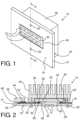
- a lighting device 10 according to the invention shown in fig. 1comprises multiple separate LEDs 12 arranged in an array (5x2 in the example shown) mounted on a printed circuit board PCB 14 as a flat carrier.
- the PCB 14has a front surface 16 and a rear surface 18.
- the flat light emitting surfaces of the LEDs 12face into the front direction, i.e. outward from the front surface 16.
- an electrical circuit for the LEDs 12is provided on the rear surface 18 of the PCB 14, including a plug connector 22 (shown schematically only) and conductor tracks (24) provided as a copper layer on the rear surface 18.
- the LEDs 12are mounted on a ceramic (AlN) mounting element 30, which includes peripheral flat mounting portions 32 and a central elevated portion 34 projecting from the flat mounting portions 32 into the front direction.
- the LEDs 12are mounted on the elevated portion 34.
- a cutout 40is formed in the PCB 14, connecting the front surface 16 and rear surface 18.
- the cutout 40is formed as a rectangular window bordered by four straight edges.
- the mounting element 30is positioned with its mounting portions 32 on top of the rear surface 18 of the PCB 14 such that the central portion 34, which in the example shown is elevated, is arranged within the window formed by the cutout 40.
- the LEDs 12are oriented into the front direction, i.e. the light emitting surface is parallel to the front surface 16. Thus, the LEDs 12, if supplied with electrical operating power, emit light into the front direction.
- the LEDs 12are electrically connected to contact pads 36 provided on the mounting portions 32 of the mounting element 30.
- the contact pads 36are referred to as mount-side contact portions. They are provided on the same side of the mounting element 30 as the LEDs 12.
- the electrical connection to the LEDs 12is provided by flat conductors on the surface of the mounting element 30 (not shown).
- the mounting element 30is made of AlN as electrically insulating ceramic material with relatively good heat conduction to dissipate heat generated by the LEDs 12 in operation.
- the mounting element 30is positioned on the rear surface 18 of the PCB 14 such that the mount-side contact pads 36 are arranged directly opposed to carrier-side contact pads 26 on the rear surface 18 of the PCB 14.
- the carrier-side contact pads 26are electrically connected or formed as parts of the conductor tracks 24 provided on the rear surface 18.
- the mount-side contact pads 36 and carrier-side contact pads 26are arranged on top of each other forming contact pairs. They are electrically connected by solder layers 42 provided in between.
- the plug connector 22also comprises contact pads 44 arranged opposite to contact pads 46 formed as part of the conductor tracks 24 on the rear surface 18 of the PCB 14.
- a solder connection 48is formed.
- the LEDs 12are electrically connected via the solder connection between the mount-side and carrier-side contact pads 36, 26, the conductor tracks 24, and the solder connection 48 to the plug connector 44.
- the LEDsmay thus be operated by supplying electrical operating power from the plug connector 44 through the described connection path.
- the LEDs 12are each separately operable.
- the array of LEDs 12may e.g. be used in a vehicle headlight as matrix or ADB (adaptive driving beam) light.
- Heat generated by the LEDs 12 in operationis dissipated through the thermally conductive mounting element 30 and further through the heat sink 20 mounted to the backside of the mounting element 30 and connected by a heat-conducting layer 50 e.g. of heat conductive paste or glue.
- the heat sink 20is fixed to the PCB 14 by screws 52.
- Fig. 3a, 3bshow steps of manufacturing the lighting device 10.
- the PCB 14is provided with the conductor tracks 24 forming contact pads 26, 46 on the rear surface 18 on both sides of the cutout 40.
- Solder paste 42, 48is provided on the contact pads 26, 46.
- the mounting element 30is reverse mounted on the rear surface 18 of the PCB 14 with both the LEDs 12 and the mount-side contact pads 36 facing in front direction.
- the mounting elementis placed onto the rear surface 18 of the PCB 14 such that the mount-side and carrier-side contact pads 26, 36 are placed directly on top of each other, with the solder paste 42 in between.
- the placement of the mounting element 30is such that the central portion 34 on which the LEDs 12 are mounted is placed within the window formed by the cutout 40.
- the plug connector 22is also placed on the rear surface 18 of the PCB 14 with the contact pads 44 and 46 facing each other with interposed solder paste 48.
- the entire assembly 10is then subjected to reflow soldering, such that the solder paste 42, 48 melts and provides solder connections between the opposed contact pads 26, 36, 44, 46, thus fixing the mounting element 30 in the reverse mounted position.
- the heat sink 20is placed on the rear surface 18 of the PCB 14 with the interposed layer 50 and fixed by screws 52 such that the back surface of the mounting element 30 is in thermal contact with the heat sink 20.
- Fig. 4, 5show alternative second and third embodiments of lighting devices.
- the second and third embodimentcorrespond to the lighting device 10 according to the first embodiment. In the following, only differences will be explained.
- Like reference numeralsrefer to like parts.
- the mounting element 30is entirely flat, i.e. the central portion where the LEDs 12 are mounted is not raised.
- the LEDs 12are provided over the cutout 40 to emit light through the window formed by the cutout 40 into the front direction.
- the mounting element 30is provided with a mounting portion 32 only on one side of the cutout 40, not on both sides as in the first embodiment 10.
- the 5x2 array of LEDs 12 shown in Fig. 1is only one example of an arrangement of LEDs 12 on the mounting element 30.
- lighting devicesmay comprise more or fewer LEDs, and the LEDs 12 may be arranged differently.
- the rear surface 18 of the PCB 14only comprises an electrical circuit including conductor tracks 24 and the plug connector 22, it is also possible to provide further electrical components forming a different electrical circuit on the PCB 14.
- cutout 40 in the example shownis a rectangular hole in the PCB 14 entirely bordered on four edges of the PCB 14, the cutout 40 may be shaped differently, and may e.g. be formed at an outer edge of the PCB 14, such that it may not be entirely surrounded by the PCB 14 to all sides.
- the mounting element 30may be made of different material or different materials.
- the mounting elementmay comprise a portion, e.g. a core, made of a material of good heat conduction, e.g. a metal such as Aluminum, Copper or other metals, including alloys containing Copper.
- a material of good heat conductione.g. a metal such as Aluminum, Copper or other metals, including alloys containing Copper.
- the coremay preferably be fully or partially covered by an insulating body or layer, such that the LEDs 12 and/or conductors connecting the LEDs to the mount-side contact pads 36 may be electrically insulated from the core.
- the insulating body or layermay be designed to still achieve good heat conduction, e.g. by choosing a low thickness and/or an insulating material of good heat conduction, e.g. a ceramic material.
- any reference signsshall not be construed as limiting the claims.
- the word “comprising”does not exclude the presence of elements or steps other than those listed in the claims.
- the indefinite article “a” or “an” preceding an elementdoes not exclude the presence of a plurality of such elements.
- the mere fact that certain measures are recited in mutually different dependent claimsdoes not indicate that a combination of these measures cannot be used to advantage.
Landscapes
- Engineering & Computer Science (AREA)
- Microelectronics & Electronic Packaging (AREA)
- Power Engineering (AREA)
- General Physics & Mathematics (AREA)
- Computer Hardware Design (AREA)
- Condensed Matter Physics & Semiconductors (AREA)
- Physics & Mathematics (AREA)
- General Engineering & Computer Science (AREA)
- Chemical & Material Sciences (AREA)
- Ceramic Engineering (AREA)
- Arrangement Of Elements, Cooling, Sealing, Or The Like Of Lighting Devices (AREA)
- Led Device Packages (AREA)
- Non-Portable Lighting Devices Or Systems Thereof (AREA)
Description
- The invention relates to a lighting device and a method of manufacturing a lighting device. More particularly, the invention relates to a lighting device mounted on a flat carrier.
- Flat carriers such as circuit boards are widely used to mount electrical components. By conductor tracks provided on a circuit board interconnecting mounted electrical components, electrical circuits are formed. Circuit boards are generally made of electrically non-conductive material such as fiber reinforced epoxy material. Conductive tracks may be e.g. provided as laminated copper sheets on one side or on both sides of the flat carrier.
- LED elements, which are increasingly used for lighting purposes, may be mounted on a circuit board e.g. by SMD solder connection.
- Reference
US2011/0215354 A1 shows a light-emitting device (LED) package component including an LED chip and a carrier chip. The carrier chip comprises four bond pads on a surface of the carrier chip, wherein the third and fourth bond pad are electrically connected to the first and the second bond pads, respectively. The first, the second, the third, and the fourth bond pad are arranged on a same surface of the carrier chip. The LED package component further includes a first and a second metal bump bonding the first and the second bond pads, respectively, onto the LED chip through flip-chip bonding. Additionally, a window-type module substrate is bonded onto the third and the fourth bond pads through flip-chip bonding. The window-type module substrate includes a window, wherein the LED chip is configured to emit light toward the window. ReferenceWO 2006 / 105 644 A1 shows a mounting assembly for one or more light-emitting elements, wherein the mounting assembly is configured such that the one or more light-emitting elements are inferiorly connected to a carrier. The carrier comprises one or more light transmission regions, wherein each of the one or more light-emitting elements is aligned with a light transmission region enabling light to pass through the carrier. The inferior mounting of the light-emitting elements can provide ease of thermal access to a cooling interface associated with the one or more light-emitting elements by a thermal management system. US2014/0124823 A1 discloses a light-emitting apparatus package including an electrically insulated ceramic substrate, a first concave section formed in the direction of thickness of the ceramic substrate so as to form a light exit aperture in a surface of the ceramic substrate, a second concave section formed within the first concave section in the further direction of thickness of the ceramic substrate so that one or more light-emitting devices are provided therein, and a wiring pattern for supplying electricity, which is provided in the first concave section.WO 2006/105644 A1 discloses a mounting assembly for one or more light-emitting elements, wherein the mounting assembly is configured such that the one or more light-emitting elements are inferiorly connected to a carrier. The carrier comprises one or more light transmission regions, wherein each of the one or more light-emitting elements is aligned with a light transmission region enabling light to pass through the carrier.US2011/0215354 A1 discloses a light-emitting device (LED) package component including an LED chip and a carrier chip. The carrier chip includes a first and a second bond pad on a surface of the carrier chip; and a third and a fourth bond pad on the surface of the carrier chip and electrically connected to the first and the second bond pads, respectively. The first, the second, the third, and the fourth bond pads are on a same surface of the carrier chip. The LED package component further includes a first and a second metal bump bonding the first and the second bond pads, respectively, onto the LED chip through flip-chip bonding; and a window-type module substrate bonded onto the third and the fourth bond pads through flip-chip bonding. The window-type module substrate includes a window, with the LED chip configured to emit light toward the window.US 9 252 337 B1 - It may be considered an object to propose a lighting device and a method of manufacturing thereof which allows to easily mount LED elements on a flat carrier in a way well suited for lighting applications.
- This may be achieved by a lighting device according to claim 1 and a manufacturing method according to claim 11. Dependent claims refer to preferred embodiments.
- The present inventors have considered that LED elements with sufficient operating power to be used in lighting applications require, besides electrical connection, a thermal interface allowing to dissipate heat generated in operation. While this may be addressed by using material with good heat conduction, such as ceramic substrates, as carrier for the LED elements, it would significantly increase cost to provide additional components such as connectors or driver electronics on the expensive ceramic substrate. In particular, cost and size increase for multiple LED elements.
- The inventors have recognized that both electrical and thermal connection may be simplified if an LED element is not as usual mounted to face away from the carrier surface it is mounted on, but if the LED element is mounted in reverse fashion.
- The lighting device according to the invention includes a flat carrier with opposed front and rear surfaces. In particular, the flat carrier may be a circuit board made out of any material, preferably electrically insulating material, in particular of a plastic material. Electrical contact portions are provided on at least one of the surfaces of the flat carrier, which will be referred to as a rear surface. Each electrical contact portion comprises an element made out of an electrically conductive material, such as a metal, in particular copper. The contact portion provided on the rear surface of the carrier will be further referred to as carrier-side electrical contact portion. According to the invention, the contact portions are provided as a flat contact pad.
- The flat carrier according to the invention comprises a cutout. The cutout is a passage between the front and rear surfaces. The cutout comprises a cutout area which may be bordered e.g. by at least two, preferably three or more, further preferred four or more cutout edges formed by portions of the flat carrier. The edges may preferably be straight. Preferably, the cutout is formed as a hole in the flat carrier, which may be fully enclosed by the carrier material.
- Multiple LED elements are provided on a mounting element. The term "LED element" here refers to any kind of solid-state lighting element or elements, such as in particular light emitting diodes, organic light emitting diodes, laser diodes, etc. An LED element may be comprised of a single solid-state lighting element or of a plurality of such solid-state lighting elements arranged closely together.
- The mounting element is preferably made of an electrically insulating material, further preferably different from the material of the flat carrier. For example, the mounting element may be made out of a ceramic material, such as in particular AlN. Multiple electrical contact portions, which will be referred to as a mount-side electrical contact portions, are according to the invention provided as contact pads on the mounting element and are electrically connected to the LED elements thereon, e.g. by conductors provided on the surface of the mounting element.
- According to the invention, the mounting element, or at least a portion thereof, is arranged on the rear surface of the carrier such that an electrical contact is formed between the carrier-side electrical contact portions and the mount-side electrical contact portions. According to the invention, the mount-side and carrier-side electrical contact portions are arranged directly on top of each other, either in direct contact or connected by an electrically conductive connection, such as a solder connection.
- The mounting element is positioned relative to the carrier such that the LED elements are arranged on or within the cutout, such that light is emitted into the front direction. According to the invention the mounting element comprises an elevated portion and the elevated portion is arranged projecting into or covering the cutout, such that the LED element provided thereon is either arranged behind a window defined by the cutout or projects into or even through this window. Thus, a light emitting portion of the LED element may face into the front direction, i.e. opposed to the rear surface on which the mount-side contact element is connected. Thus, the arrangement of the mounting element may be referred to as reverse mounting.
- Further, a heat sink element is positioned in thermal contact with the mounting element. The heat sink element is positioned to the rear of the mounting element, such that it may be positioned on or above the rear surface of the carrier. The heat sink element preferably includes a material of high thermal conductivity, such as a metal, in particular copper.
- The proposed lighting device and manufacturing method allow to easily mount an LED element on a flat carrier, such as a circuit board. Conventional positioning and connection techniques available e.g. for SMD components may be used, such as soldering and in particular reflow soldering. A high accuracy of placement may thus be achieved. As will be further explained below, the reverse mounting concept is in particular advantageous for multiple separately operable LED elements, such as a line or array of LED elements. Since the mounting element may be kept small and usual circuit board materials may be used for the carrier, a relatively inexpensive assembly may be formed.
- According to the invention, the LED elements and the mount-side contact portions are arranged on the same side of the mounting element. Both the mount-side contact portions and the light emitting portion of the LED elements preferably face in the front direction.
- According to the invention, the mounting element is provided with multiple LED elements, and multiple mount-side electrical contact portions connected to the LED elements. Corresponding to the mount-side electrical contact portions, multiple carrier-side electrical contact portions are provided on the rear surface of the flat carrier. The mount-side and carrier-side electrical contact portions are then provided in electrical contact with each other, such that an electrical connection to each of the LED elements may be established. Thus, it is possible to provide multiple separately operable LED elements, which may be turned off or on independently of one another, although they may share one common terminal. This concept is applicable to a single LED element, but also e.g. to 2, 3 or more separate LED elements, preferably 5 or more, further preferred 10 or more. The concept may even be used for large numbers of e.g. up to 1000 or up to 500 LED elements, and preferably up to 100 LED elements. In particular for multiple LED elements, the reverse mounted arrangement and electrical contacting via mount-side and carrier-side contact portions allows a very compact structure and easy manufacturing even for a large number of LED elements.
- The contact portions may all be provided on the rear surface of the flat carrier on one side of the cutout, e.g. along one edge of the cutout. It is, however, preferred to provide electrical contact portions to more than one side of the cutout, in particular on opposite sides thereof, or surrounding the cutout on all sides. In the preferred embodiment, a first carrier-side electrical contact portion is connected to a first mount-side electrical contact portion and a second carrier-side electrical contact portion is connected to a second mount-side electrical contact portion. The first carrier-side and mount-side electrical contact portions are separated from the second carrier-side and mount-side electrical contact portions by the cutout. This makes efficient use of the available space for the arrangement of the contact portions, in particular for a larger number of LED elements.
- In a preferred embodiment, electrical conductor portions may be provided on the rear surface of the carrier, in particular flat conductor tracks. The conductor portions may be connected to the carrier-side contact portion. An electrical circuit may be provided on the rear surface of the carrier, electrically connected to the carrier-side contact portion. The electrical circuit may comprise one or more electrical component and/or one or more electrical plug connector. The components of the circuit may be interconnected by electrical conductor portions. In particular, the electrical circuit may be a driver circuit disposed to provide electrical operating power to the LED element.
- The mounting element preferably includes one or more flat mounting portion which may be arranged on the rear surface of the carrier. The mounting element comprises at least one elevated portion, which is arranged to at least partly project into the cutout. The LED elements are arranged on the elevated portion. Depending on the height of the elevated portion, the LED element may be provided within the cutout, or at least substantially level with the front surface of the carrier, or may even project from the front surface.
- The heat sink element may preferably be fixed to the carrier, e.g. held by a material connection such as by gluing or soldering, or by a mechanical connection, such as by one or more screws, clamps etc. Fixing the heat sink element to the carrier instead of to the mounting element only provides a large surface for a secure connection.
- In a preferred embodiment, the mounting element may comprise a plane rear surface, which may be larger than the cutout. The heat sink element may be provided to cover the rear surface, providing for good thermal contact.
- These and other aspects of the invention will be apparent from and elucidated with reference to the embodiments described hereinafter.
Fig. 1 shows a perspective view of a lighting device according to a first embodiment in accordance with the invention;Fig. 2 shows a cross-section of the lighting device offig. 1 along A.. A;Fig. 3a, 3b show stages of assembly of the lighting device offig. 1, fig. 2 ;Fig. 4 shows a cross-sectional view of a lighting device according to a second embodiment, not in accordance with the invention as claimed;Fig. 5 shows a cross-sectional view of a lighting device according to a third embodiment in accordance with the invention.- A
lighting device 10 according to the invention shown infig. 1 comprises multipleseparate LEDs 12 arranged in an array (5x2 in the example shown) mounted on a printedcircuit board PCB 14 as a flat carrier. - The
PCB 14 has afront surface 16 and arear surface 18. The flat light emitting surfaces of theLEDs 12 face into the front direction, i.e. outward from thefront surface 16. - As shown in the cross-sectional view of
fig. 2 , an electrical circuit for theLEDs 12 is provided on therear surface 18 of thePCB 14, including a plug connector 22 (shown schematically only) and conductor tracks (24) provided as a copper layer on therear surface 18. - The
LEDs 12 are mounted on a ceramic (AlN) mountingelement 30, which includes peripheral flat mountingportions 32 and a centralelevated portion 34 projecting from theflat mounting portions 32 into the front direction. TheLEDs 12 are mounted on theelevated portion 34. - A
cutout 40 is formed in thePCB 14, connecting thefront surface 16 andrear surface 18. In the example shown, thecutout 40 is formed as a rectangular window bordered by four straight edges. - The mounting
element 30 is positioned with its mountingportions 32 on top of therear surface 18 of thePCB 14 such that thecentral portion 34, which in the example shown is elevated, is arranged within the window formed by thecutout 40. TheLEDs 12 are oriented into the front direction, i.e. the light emitting surface is parallel to thefront surface 16. Thus, theLEDs 12, if supplied with electrical operating power, emit light into the front direction. - The
LEDs 12 are electrically connected to contactpads 36 provided on the mountingportions 32 of the mountingelement 30. Thecontact pads 36 are referred to as mount-side contact portions. They are provided on the same side of the mountingelement 30 as theLEDs 12. The electrical connection to theLEDs 12 is provided by flat conductors on the surface of the mounting element 30 (not shown). - In the preferred example, the mounting
element 30 is made of AlN as electrically insulating ceramic material with relatively good heat conduction to dissipate heat generated by theLEDs 12 in operation. - The mounting
element 30 is positioned on therear surface 18 of thePCB 14 such that the mount-side contact pads 36 are arranged directly opposed to carrier-side contact pads 26 on therear surface 18 of thePCB 14. The carrier-side contact pads 26 are electrically connected or formed as parts of the conductor tracks 24 provided on therear surface 18. - The mount-
side contact pads 36 and carrier-side contact pads 26 are arranged on top of each other forming contact pairs. They are electrically connected bysolder layers 42 provided in between. - The
plug connector 22 also comprisescontact pads 44 arranged opposite to contactpads 46 formed as part of the conductor tracks 24 on therear surface 18 of thePCB 14. Here also, asolder connection 48 is formed. - Thus, the
LEDs 12 are electrically connected via the solder connection between the mount-side and carrier-side contact pads solder connection 48 to theplug connector 44. The LEDs may thus be operated by supplying electrical operating power from theplug connector 44 through the described connection path. As each of theLEDs 12 is connected to one of the mount-side contact pads 36 (with a common ground connection), theLEDs 12 are each separately operable. The array ofLEDs 12 may e.g. be used in a vehicle headlight as matrix or ADB (adaptive driving beam) light. - Heat generated by the
LEDs 12 in operation is dissipated through the thermally conductive mountingelement 30 and further through theheat sink 20 mounted to the backside of the mountingelement 30 and connected by a heat-conductinglayer 50 e.g. of heat conductive paste or glue. - The
heat sink 20 is fixed to thePCB 14 byscrews 52. Fig. 3a, 3b show steps of manufacturing thelighting device 10. ThePCB 14 is provided with the conductor tracks 24 formingcontact pads rear surface 18 on both sides of thecutout 40.Solder paste contact pads element 30 is reverse mounted on therear surface 18 of thePCB 14 with both theLEDs 12 and the mount-side contact pads 36 facing in front direction.- The mounting element is placed onto the
rear surface 18 of thePCB 14 such that the mount-side and carrier-side contact pads solder paste 42 in between. The placement of the mountingelement 30 is such that thecentral portion 34 on which theLEDs 12 are mounted is placed within the window formed by thecutout 40. - The
plug connector 22 is also placed on therear surface 18 of thePCB 14 with thecontact pads solder paste 48. - The
entire assembly 10 is then subjected to reflow soldering, such that thesolder paste opposed contact pads element 30 in the reverse mounted position. - In a further step (not shown), the
heat sink 20 is placed on therear surface 18 of thePCB 14 with the interposedlayer 50 and fixed byscrews 52 such that the back surface of the mountingelement 30 is in thermal contact with theheat sink 20. Fig. 4, 5 show alternative second and third embodiments of lighting devices. The second and third embodiment correspond to thelighting device 10 according to the first embodiment. In the following, only differences will be explained. Like reference numerals refer to like parts.- In the second embodiment, which falls outside the invention as claimed and which is shown in
Fig. 4 , the mountingelement 30 is entirely flat, i.e. the central portion where theLEDs 12 are mounted is not raised. TheLEDs 12 are provided over thecutout 40 to emit light through the window formed by thecutout 40 into the front direction. - According to the third embodiment of the invention, shown in
Fig. 5 , the mountingelement 30 is provided with a mountingportion 32 only on one side of thecutout 40, not on both sides as in thefirst embodiment 10. - While the invention has been illustrated and described in detail in the drawings and forgoing description, such illustration and description are to be considered illustrative or exemplary and not restrictive; the invention is not limited to the disclosed embodiments.
- For example, the 5x2 array of
LEDs 12 shown inFig. 1 is only one example of an arrangement ofLEDs 12 on the mountingelement 30. In different embodiments, lighting devices may comprise more or fewer LEDs, and theLEDs 12 may be arranged differently. - While in the embodiments shown the
rear surface 18 of thePCB 14 only comprises an electrical circuit including conductor tracks 24 and theplug connector 22, it is also possible to provide further electrical components forming a different electrical circuit on thePCB 14. - While the
cutout 40 in the example shown is a rectangular hole in thePCB 14 entirely bordered on four edges of thePCB 14, thecutout 40 may be shaped differently, and may e.g. be formed at an outer edge of thePCB 14, such that it may not be entirely surrounded by thePCB 14 to all sides. - In alternative embodiments, the mounting
element 30 may be made of different material or different materials. In particular, the mounting element may comprise a portion, e.g. a core, made of a material of good heat conduction, e.g. a metal such as Aluminum, Copper or other metals, including alloys containing Copper. If the core is electrically conductive, it may preferably be fully or partially covered by an insulating body or layer, such that theLEDs 12 and/or conductors connecting the LEDs to the mount-side contact pads 36 may be electrically insulated from the core. The insulating body or layer may be designed to still achieve good heat conduction, e.g. by choosing a low thickness and/or an insulating material of good heat conduction, e.g. a ceramic material. - In the claims, any reference signs shall not be construed as limiting the claims. The word "comprising" does not exclude the presence of elements or steps other than those listed in the claims. The indefinite article "a" or "an" preceding an element does not exclude the presence of a plurality of such elements. The mere fact that certain measures are recited in mutually different dependent claims does not indicate that a combination of these measures cannot be used to advantage.
Claims (12)
- Lighting device, including- a flat carrier (14) with front and rear surfaces (16, 18) facing in opposed front and rear directions, said flat carrier (14) comprising a cutout (40), and said flat carrier (14) being provided with multiple carrier-side electrical contact portions (26),- a mounting element (30) comprising multiple separately operable LED elements (12) and multiple mount-side electrical contact portions (36) electrically connected to said LED elements (12),- said mounting element (30) being arranged on said rear surface (18) of said flat carrier (14) such that said LED elements (12) are arranged on or within said cutout (40) and such that an electrical contact is formed with said multiple carrier-side electrical contact portions (26) to emit light into said front direction,- and a heat sink element (20) being positioned to the rear of said mounting element (30) in thermal contact therewith,wherein said multiple carrier-side electrical portions (26) are provided on said rear surface (18) of said flat carrier (14),wherein said electric contact is formed between said carrier side electric contact portions (26) and said mount-side electrical contact portions (36),wherein said carrier-side electrical contact portions (26) and said mount-side electrical contact portions (36) are respectively provided as contact pads (26, 36) and are arranged on top of each other forming respective contact pairs,wherein said mounting element (30) comprises an elevated portion (34) projecting into said cutout (40);wherein said LED elements (12) are arranged on said elevated portion (34); andwherein said mount-side electrical contact portions (36) and said LED elements (12) are provided on the same side of said mounting element (30).
- Lighting device according to claim 2, wherein- at least a first carrier-side electrical contact portion (26) is provided connected to a first mount-side electrical contacted portion (36) and a second carrier-side electrical contact portion (26) is provided connected to a second mount-side electrical contact portion (36),- wherein said first carrier-side and mount-side electrical contact portions (26, 36) are separated from said second carrier-side and mount-side electrical contact portions (26, 36) by said cutout (40).
- Lighting device according to one of the above claims, wherein- said mounting element (30) is made of a ceramic material.
- Lighting device according to one of the above claims, wherein- said heat sink (20) is made of a metal material.
- Lighting device according to one of the above claims, wherein- said carrier (14) is made of a plastic material.
- Lighting device according to one of the above claims, wherein- said mount-side electrical contact portion (26) is connected to said carrier-side electrical contact portion (36) by a solder connection.
- Lighting device according to one of the above claims, wherein- electrical conductor portions (24) are provided on said rear surface (18), connected to said carrier-side contact portions (26).
- Lighting device according to one of the above claims, wherein- an electrical circuit is provided on said rear surface (18), electrically connected to said carrier-side contact portions (26),- said electrical circuit comprising at least one electrical component and/or an electrical plug connector (22).
- Lighting device according to one of the above claims, wherein- said heat sink element (20) is fixed to said carrier (14).
- Lighting device according to one of the above claims, wherein- said mounting element (30) comprises a plane rear surface larger than said cutout (40),- said heat sink element (30) being provided to cover said rear surface.
- Method of manufacturing a lighting device (10) including- providing a flat carrier (14) with front and rear surfaces (16, 18) facing in opposed front and rear directions, said flat carrier (14) comprising a cutout (40), and said flat carrier being provided with multiple carrier-side electrical contact portions (26),- providing a mounting element (30) comprising multiple separately operable LED elements (12) and multiple mount-side electrical contact portions (36) electrically connected to said LED elements (12),- arranging said mounting element (30) on said rear surface (18) of said flat carrier (14) such that said LED elements are arranged on or within said cutout (40) and such that an electrical contact is formed with said multiple carrier-side contact portions (26), to emit light into said front direction,- and positioning a heat sink element (20) to the rear of said mounting element (30) in thermal contact therewith,wherein said multiple carrier-side electrical portions (26) are provided on said rear surface (18) of said flat carrier (14),wherein said electric contact is formed between said carrier side electric contact portions (26) and said mount-side electrical contact portions (36),wherein said carrier-side electrical contact portions (26) and said mount-side electrical contact portions (36) are respectively provided as contact pads (26, 36) and are arranged on top of each other forming respective contact pairs,wherein said mounting element (30) comprises an elevated portion (34) projecting into said cutout (40);wherein said LED elements (12) are arranged on said elevated portion (34); andwherein said mount-side electrical contact portions (36) and said LED elements (12) are provided on the same side of said mounting element (30).
- Method according to claim 11, further including- forming a solder connection (42) between said carrier-side electrical contact portions (26) and said mount-side electrical contact portions (36).
Applications Claiming Priority (2)
| Application Number | Priority Date | Filing Date | Title |
|---|---|---|---|
| EP17161975 | 2017-03-21 | ||
| PCT/EP2018/056340WO2018172152A1 (en) | 2017-03-21 | 2018-03-14 | Mounting an led element on a flat carrier |
Publications (2)
| Publication Number | Publication Date |
|---|---|
| EP3602626A1 EP3602626A1 (en) | 2020-02-05 |
| EP3602626B1true EP3602626B1 (en) | 2023-05-03 |
Family
ID=58412882
Family Applications (1)
| Application Number | Title | Priority Date | Filing Date |
|---|---|---|---|
| EP18711097.8AActiveEP3602626B1 (en) | 2017-03-21 | 2018-03-14 | Lighting device with led elements on a mounting element on a flat carrier and method of manufacturing the same |
Country Status (6)
| Country | Link |
|---|---|
| US (1) | US11056629B2 (en) |
| EP (1) | EP3602626B1 (en) |
| JP (1) | JP7320452B2 (en) |
| KR (1) | KR102503462B1 (en) |
| CN (1) | CN110431664B (en) |
| WO (1) | WO2018172152A1 (en) |
Cited By (1)
| Publication number | Priority date | Publication date | Assignee | Title |
|---|---|---|---|---|
| EP4082041A1 (en)* | 2019-12-27 | 2022-11-02 | Lumileds LLC | Light-emitting diode (led) package assembly, vehicle headlamp system comprising a light-emitting diode (led) package assembly, and method of manufacturing a light-emitting diode (led) package assembly |
Families Citing this family (12)
| Publication number | Priority date | Publication date | Assignee | Title |
|---|---|---|---|---|
| FR3087246B1 (en)* | 2018-10-15 | 2022-12-16 | Valeo Vision | MATRIX LIGHT SOURCE WITH ADJUSTABLE ARCHITECTURE |
| CN109538998B (en)* | 2018-12-29 | 2024-02-06 | 广州纽威光电科技有限公司 | LED lamp |
| US11626448B2 (en) | 2019-03-29 | 2023-04-11 | Lumileds Llc | Fan-out light-emitting diode (LED) device substrate with embedded backplane, lighting system and method of manufacture |
| US11631594B2 (en) | 2019-11-19 | 2023-04-18 | Lumileds Llc | Fan out structure for light-emitting diode (LED) device and lighting system |
| US11664347B2 (en) | 2020-01-07 | 2023-05-30 | Lumileds Llc | Ceramic carrier and build up carrier for light-emitting diode (LED) array |
| EP4118689A4 (en)* | 2020-03-10 | 2024-01-17 | Lumileds LLC | Method of manufacturing an augmented led array assembly |
| US11476217B2 (en) | 2020-03-10 | 2022-10-18 | Lumileds Llc | Method of manufacturing an augmented LED array assembly |
| DE102020108916B4 (en)* | 2020-03-31 | 2025-05-28 | Infineon Technologies Ag | Package with clip and connector over electronic components |
| JP7556759B2 (en) | 2020-11-20 | 2024-09-26 | スタンレー電気株式会社 | Light source unit for vehicle lamp and vehicle lamp |
| EP4369088A4 (en)* | 2022-02-09 | 2024-12-25 | Samsung Electronics Co., Ltd. | CONNECTOR, PRINTED CIRCUIT BOARD HAVING A CONNECTOR MOUNTED THEREON, AND DISPLAY APPARATUS COMPRISING SAME |
| DE102022118926A1 (en)* | 2022-07-28 | 2024-02-08 | Rolls-Royce Deutschland Ltd & Co Kg | PCB assembly |
| FR3147663B1 (en)* | 2023-04-07 | 2025-04-18 | St Microelectronics Int Nv | FIXED HEAT SINK ON THE SUBSTRATE OF AN INTEGRATED CIRCUIT PACKAGE |
Citations (1)
| Publication number | Priority date | Publication date | Assignee | Title |
|---|---|---|---|---|
| US9252337B1 (en)* | 2014-12-22 | 2016-02-02 | Bridgelux, Inc. | Composite substrate for light emitting diodes |
Family Cites Families (25)
| Publication number | Priority date | Publication date | Assignee | Title |
|---|---|---|---|---|
| US5739800A (en)* | 1996-03-04 | 1998-04-14 | Motorola | Integrated electro-optical package with LED display chip and substrate with drivers and central opening |
| JP3930710B2 (en)* | 2000-09-13 | 2007-06-13 | シチズン電子株式会社 | Chip-type light emitting diode and manufacturing method thereof |
| JP2003008072A (en)* | 2001-06-25 | 2003-01-10 | Citizen Electronics Co Ltd | Light emitting diode |
| CN101740560B (en)* | 2003-04-01 | 2012-11-21 | 夏普株式会社 | Light-emitting apparatus, backlight apparatus, and display apparatus |
| JP4166611B2 (en)* | 2003-04-01 | 2008-10-15 | シャープ株式会社 | Light emitting device package, light emitting device |
| JP2004311791A (en)* | 2003-04-08 | 2004-11-04 | Sharp Corp | Lighting device, backlight device and display device |
| US7210817B2 (en)* | 2004-04-27 | 2007-05-01 | Avago Technologies Ecbu Ip (Singapore) Pte. Ltd. | Method, system and device for delivering phototherapy to a patient |
| CA2617314A1 (en) | 2005-04-05 | 2006-10-12 | Tir Technology Lp | Mounting assembly for optoelectronic devices |
| JP5055837B2 (en)* | 2006-05-26 | 2012-10-24 | 日亜化学工業株式会社 | Light emitting device |
| TWI341038B (en)* | 2006-12-18 | 2011-04-21 | Delta Electronics Inc | Electroluminescence module |
| DE102007023651A1 (en)* | 2007-05-22 | 2008-11-27 | Osram Gesellschaft mit beschränkter Haftung | Lighting device, backlight device and display device |
| CN101603636B (en) | 2008-06-10 | 2012-05-23 | 展晶科技(深圳)有限公司 | Light source device |
| CN102089567B (en)* | 2008-07-07 | 2014-02-26 | 松下电器产业株式会社 | Light source for bulb-shaped lighting |
| US8791471B2 (en)* | 2008-11-07 | 2014-07-29 | Cree Hong Kong Limited | Multi-chip light emitting diode modules |
| US8183578B2 (en)* | 2010-03-02 | 2012-05-22 | Taiwan Semiconductor Manufacturing Company, Ltd. | Double flip-chip LED package components |
| KR101495580B1 (en)* | 2010-04-26 | 2015-02-25 | 파나소닉 주식회사 | Leadframe, wiring board, light emitting unit, and illuminating apparatus |
| US8354684B2 (en)* | 2011-01-09 | 2013-01-15 | Bridgelux, Inc. | Packaging photon building blocks having only top side connections in an interconnect structure |
| DE102011115314B4 (en)* | 2011-09-29 | 2019-04-25 | Osram Opto Semiconductors Gmbh | LED module |
| WO2013065414A1 (en)* | 2011-10-31 | 2013-05-10 | シャープ株式会社 | Light-emitting device, illumination device, and method for manufacturing light-emitting device |
| US9188288B2 (en)* | 2012-09-28 | 2015-11-17 | Tsmc Solid State Lighting Ltd. | LED emitter with improved white color appearance |
| WO2014175460A1 (en)* | 2013-04-26 | 2014-10-30 | 京セラ株式会社 | Substrate for mounting electronic element and electronic device |
| JP6186904B2 (en)* | 2013-06-05 | 2017-08-30 | 日亜化学工業株式会社 | Light emitting device |
| JP6427313B2 (en)* | 2013-11-01 | 2018-11-21 | 株式会社タムラ製作所 | Light emitting device |
| JP2015177021A (en)* | 2014-03-14 | 2015-10-05 | スタンレー電気株式会社 | Semiconductor light emitting device |
| US9420658B2 (en)* | 2014-12-05 | 2016-08-16 | Xenio Corporation | Inrush energy control for a light emitter |
- 2018
- 2018-03-14USUS16/496,160patent/US11056629B2/enactiveActive
- 2018-03-14CNCN201880019846.6Apatent/CN110431664B/enactiveActive
- 2018-03-14WOPCT/EP2018/056340patent/WO2018172152A1/ennot_activeCeased
- 2018-03-14EPEP18711097.8Apatent/EP3602626B1/enactiveActive
- 2018-03-14KRKR1020197027550Apatent/KR102503462B1/enactiveActive
- 2018-03-14JPJP2019551664Apatent/JP7320452B2/enactiveActive
Patent Citations (1)
| Publication number | Priority date | Publication date | Assignee | Title |
|---|---|---|---|---|
| US9252337B1 (en)* | 2014-12-22 | 2016-02-02 | Bridgelux, Inc. | Composite substrate for light emitting diodes |
Cited By (1)
| Publication number | Priority date | Publication date | Assignee | Title |
|---|---|---|---|---|
| EP4082041A1 (en)* | 2019-12-27 | 2022-11-02 | Lumileds LLC | Light-emitting diode (led) package assembly, vehicle headlamp system comprising a light-emitting diode (led) package assembly, and method of manufacturing a light-emitting diode (led) package assembly |
Also Published As
| Publication number | Publication date |
|---|---|
| JP7320452B2 (en) | 2023-08-03 |
| CN110431664B (en) | 2024-03-26 |
| CN110431664A (en) | 2019-11-08 |
| KR20190123294A (en) | 2019-10-31 |
| US20200161519A1 (en) | 2020-05-21 |
| WO2018172152A1 (en) | 2018-09-27 |
| EP3602626A1 (en) | 2020-02-05 |
| KR102503462B1 (en) | 2023-02-24 |
| JP2020515068A (en) | 2020-05-21 |
| US11056629B2 (en) | 2021-07-06 |
Similar Documents
| Publication | Publication Date | Title |
|---|---|---|
| EP3602626B1 (en) | Lighting device with led elements on a mounting element on a flat carrier and method of manufacturing the same | |
| US20110180819A1 (en) | Light-emitting arrangement | |
| US9941258B2 (en) | LED lead frame array for general illumination | |
| US20080296599A1 (en) | LED Package with Stepped Aperture | |
| US20100033976A1 (en) | Heat dissipation module for light emitting diode | |
| JP2006253689A (en) | Mounting of LED with high heat dissipation | |
| EP2188849B1 (en) | Light emitting device | |
| US7688591B2 (en) | Electronic-component-mounting board | |
| US7911051B2 (en) | Electronic circuit arrangement and method for producing an electronic circuit arrangement | |
| US6894901B2 (en) | Light source comprising a large number of light-emitting diodes | |
| US10236429B2 (en) | Mounting assembly and lighting device | |
| US10383209B2 (en) | Electronic assembly for lighting applications, lighting device and method for producing an electronic assembly | |
| US8585247B2 (en) | Lighting device | |
| US20210071840A1 (en) | System for the electrically connecting at least one light source to an electrical power supply system | |
| US20180220536A1 (en) | Printed circuit board and printed circuit board arrangement | |
| CN109792841B (en) | Light emitting device and method of manufacturing the same | |
| US7385285B2 (en) | Light assembly | |
| EP3133332A1 (en) | Integrated led module with ims substrate | |
| US9356005B2 (en) | Package of light emitting diode with heat sink | |
| KR20130068654A (en) | The light unit |
Legal Events
| Date | Code | Title | Description |
|---|---|---|---|
| STAA | Information on the status of an ep patent application or granted ep patent | Free format text:STATUS: UNKNOWN | |
| STAA | Information on the status of an ep patent application or granted ep patent | Free format text:STATUS: THE INTERNATIONAL PUBLICATION HAS BEEN MADE | |
| PUAI | Public reference made under article 153(3) epc to a published international application that has entered the european phase | Free format text:ORIGINAL CODE: 0009012 | |
| STAA | Information on the status of an ep patent application or granted ep patent | Free format text:STATUS: REQUEST FOR EXAMINATION WAS MADE | |
| 17P | Request for examination filed | Effective date:20191021 | |
| AK | Designated contracting states | Kind code of ref document:A1 Designated state(s):AL AT BE BG CH CY CZ DE DK EE ES FI FR GB GR HR HU IE IS IT LI LT LU LV MC MK MT NL NO PL PT RO RS SE SI SK SM TR | |
| AX | Request for extension of the european patent | Extension state:BA ME | |
| DAV | Request for validation of the european patent (deleted) | ||
| DAX | Request for extension of the european patent (deleted) | ||
| RAP1 | Party data changed (applicant data changed or rights of an application transferred) | Owner name:LUMILEDS LLC | |
| STAA | Information on the status of an ep patent application or granted ep patent | Free format text:STATUS: EXAMINATION IS IN PROGRESS | |
| 17Q | First examination report despatched | Effective date:20210722 | |
| GRAP | Despatch of communication of intention to grant a patent | Free format text:ORIGINAL CODE: EPIDOSNIGR1 | |
| STAA | Information on the status of an ep patent application or granted ep patent | Free format text:STATUS: GRANT OF PATENT IS INTENDED | |
| RIC1 | Information provided on ipc code assigned before grant | Ipc:H05K 1/18 20060101ALI20221021BHEP Ipc:H05K 1/14 20060101ALI20221021BHEP Ipc:H05K 1/02 20060101ALI20221021BHEP Ipc:F21Y 105/16 20160101ALI20221021BHEP Ipc:F21V 19/00 20060101ALI20221021BHEP Ipc:F21Y 115/10 20160101ALI20221021BHEP Ipc:H01L 33/64 20100101ALI20221021BHEP Ipc:H01L 25/075 20060101AFI20221021BHEP | |
| INTG | Intention to grant announced | Effective date:20221117 | |
| GRAS | Grant fee paid | Free format text:ORIGINAL CODE: EPIDOSNIGR3 | |
| GRAA | (expected) grant | Free format text:ORIGINAL CODE: 0009210 | |
| STAA | Information on the status of an ep patent application or granted ep patent | Free format text:STATUS: THE PATENT HAS BEEN GRANTED | |
| AK | Designated contracting states | Kind code of ref document:B1 Designated state(s):AL AT BE BG CH CY CZ DE DK EE ES FI FR GB GR HR HU IE IS IT LI LT LU LV MC MK MT NL NO PL PT RO RS SE SI SK SM TR | |
| REG | Reference to a national code | Ref country code:GB Ref legal event code:FG4D | |
| REG | Reference to a national code | Ref country code:DE Ref legal event code:R096 Ref document number:602018049177 Country of ref document:DE | |
| REG | Reference to a national code | Ref country code:AT Ref legal event code:REF Ref document number:1565397 Country of ref document:AT Kind code of ref document:T Effective date:20230515 Ref country code:CH Ref legal event code:EP | |
| REG | Reference to a national code | Ref country code:IE Ref legal event code:FG4D | |
| REG | Reference to a national code | Ref country code:LT Ref legal event code:MG9D | |
| REG | Reference to a national code | Ref country code:NL Ref legal event code:MP Effective date:20230503 | |
| REG | Reference to a national code | Ref country code:AT Ref legal event code:MK05 Ref document number:1565397 Country of ref document:AT Kind code of ref document:T Effective date:20230503 | |
| PG25 | Lapsed in a contracting state [announced via postgrant information from national office to epo] | Ref country code:SE Free format text:LAPSE BECAUSE OF FAILURE TO SUBMIT A TRANSLATION OF THE DESCRIPTION OR TO PAY THE FEE WITHIN THE PRESCRIBED TIME-LIMIT Effective date:20230503 Ref country code:PT Free format text:LAPSE BECAUSE OF FAILURE TO SUBMIT A TRANSLATION OF THE DESCRIPTION OR TO PAY THE FEE WITHIN THE PRESCRIBED TIME-LIMIT Effective date:20230904 Ref country code:NO Free format text:LAPSE BECAUSE OF FAILURE TO SUBMIT A TRANSLATION OF THE DESCRIPTION OR TO PAY THE FEE WITHIN THE PRESCRIBED TIME-LIMIT Effective date:20230803 Ref country code:NL Free format text:LAPSE BECAUSE OF FAILURE TO SUBMIT A TRANSLATION OF THE DESCRIPTION OR TO PAY THE FEE WITHIN THE PRESCRIBED TIME-LIMIT Effective date:20230503 Ref country code:ES Free format text:LAPSE BECAUSE OF FAILURE TO SUBMIT A TRANSLATION OF THE DESCRIPTION OR TO PAY THE FEE WITHIN THE PRESCRIBED TIME-LIMIT Effective date:20230503 Ref country code:AT Free format text:LAPSE BECAUSE OF FAILURE TO SUBMIT A TRANSLATION OF THE DESCRIPTION OR TO PAY THE FEE WITHIN THE PRESCRIBED TIME-LIMIT Effective date:20230503 | |
| PG25 | Lapsed in a contracting state [announced via postgrant information from national office to epo] | Ref country code:RS Free format text:LAPSE BECAUSE OF FAILURE TO SUBMIT A TRANSLATION OF THE DESCRIPTION OR TO PAY THE FEE WITHIN THE PRESCRIBED TIME-LIMIT Effective date:20230503 Ref country code:PL Free format text:LAPSE BECAUSE OF FAILURE TO SUBMIT A TRANSLATION OF THE DESCRIPTION OR TO PAY THE FEE WITHIN THE PRESCRIBED TIME-LIMIT Effective date:20230503 Ref country code:LV Free format text:LAPSE BECAUSE OF FAILURE TO SUBMIT A TRANSLATION OF THE DESCRIPTION OR TO PAY THE FEE WITHIN THE PRESCRIBED TIME-LIMIT Effective date:20230503 Ref country code:LT Free format text:LAPSE BECAUSE OF FAILURE TO SUBMIT A TRANSLATION OF THE DESCRIPTION OR TO PAY THE FEE WITHIN THE PRESCRIBED TIME-LIMIT Effective date:20230503 Ref country code:IS Free format text:LAPSE BECAUSE OF FAILURE TO SUBMIT A TRANSLATION OF THE DESCRIPTION OR TO PAY THE FEE WITHIN THE PRESCRIBED TIME-LIMIT Effective date:20230903 Ref country code:HR Free format text:LAPSE BECAUSE OF FAILURE TO SUBMIT A TRANSLATION OF THE DESCRIPTION OR TO PAY THE FEE WITHIN THE PRESCRIBED TIME-LIMIT Effective date:20230503 Ref country code:GR Free format text:LAPSE BECAUSE OF FAILURE TO SUBMIT A TRANSLATION OF THE DESCRIPTION OR TO PAY THE FEE WITHIN THE PRESCRIBED TIME-LIMIT Effective date:20230804 | |
| PG25 | Lapsed in a contracting state [announced via postgrant information from national office to epo] | Ref country code:FI Free format text:LAPSE BECAUSE OF FAILURE TO SUBMIT A TRANSLATION OF THE DESCRIPTION OR TO PAY THE FEE WITHIN THE PRESCRIBED TIME-LIMIT Effective date:20230503 | |
| PG25 | Lapsed in a contracting state [announced via postgrant information from national office to epo] | Ref country code:SK Free format text:LAPSE BECAUSE OF FAILURE TO SUBMIT A TRANSLATION OF THE DESCRIPTION OR TO PAY THE FEE WITHIN THE PRESCRIBED TIME-LIMIT Effective date:20230503 | |
| PG25 | Lapsed in a contracting state [announced via postgrant information from national office to epo] | Ref country code:SM Free format text:LAPSE BECAUSE OF FAILURE TO SUBMIT A TRANSLATION OF THE DESCRIPTION OR TO PAY THE FEE WITHIN THE PRESCRIBED TIME-LIMIT Effective date:20230503 Ref country code:SK Free format text:LAPSE BECAUSE OF FAILURE TO SUBMIT A TRANSLATION OF THE DESCRIPTION OR TO PAY THE FEE WITHIN THE PRESCRIBED TIME-LIMIT Effective date:20230503 Ref country code:RO Free format text:LAPSE BECAUSE OF FAILURE TO SUBMIT A TRANSLATION OF THE DESCRIPTION OR TO PAY THE FEE WITHIN THE PRESCRIBED TIME-LIMIT Effective date:20230503 Ref country code:EE Free format text:LAPSE BECAUSE OF FAILURE TO SUBMIT A TRANSLATION OF THE DESCRIPTION OR TO PAY THE FEE WITHIN THE PRESCRIBED TIME-LIMIT Effective date:20230503 Ref country code:DK Free format text:LAPSE BECAUSE OF FAILURE TO SUBMIT A TRANSLATION OF THE DESCRIPTION OR TO PAY THE FEE WITHIN THE PRESCRIBED TIME-LIMIT Effective date:20230503 Ref country code:CZ Free format text:LAPSE BECAUSE OF FAILURE TO SUBMIT A TRANSLATION OF THE DESCRIPTION OR TO PAY THE FEE WITHIN THE PRESCRIBED TIME-LIMIT Effective date:20230503 | |
| REG | Reference to a national code | Ref country code:DE Ref legal event code:R097 Ref document number:602018049177 Country of ref document:DE | |
| PLBE | No opposition filed within time limit | Free format text:ORIGINAL CODE: 0009261 | |
| STAA | Information on the status of an ep patent application or granted ep patent | Free format text:STATUS: NO OPPOSITION FILED WITHIN TIME LIMIT | |
| 26N | No opposition filed | Effective date:20240206 | |
| PG25 | Lapsed in a contracting state [announced via postgrant information from national office to epo] | Ref country code:SI Free format text:LAPSE BECAUSE OF FAILURE TO SUBMIT A TRANSLATION OF THE DESCRIPTION OR TO PAY THE FEE WITHIN THE PRESCRIBED TIME-LIMIT Effective date:20230503 | |
| PG25 | Lapsed in a contracting state [announced via postgrant information from national office to epo] | Ref country code:SI Free format text:LAPSE BECAUSE OF FAILURE TO SUBMIT A TRANSLATION OF THE DESCRIPTION OR TO PAY THE FEE WITHIN THE PRESCRIBED TIME-LIMIT Effective date:20230503 Ref country code:IT Free format text:LAPSE BECAUSE OF FAILURE TO SUBMIT A TRANSLATION OF THE DESCRIPTION OR TO PAY THE FEE WITHIN THE PRESCRIBED TIME-LIMIT Effective date:20230503 | |
| REG | Reference to a national code | Ref country code:CH Ref legal event code:PL | |
| PG25 | Lapsed in a contracting state [announced via postgrant information from national office to epo] | Ref country code:BG Free format text:LAPSE BECAUSE OF FAILURE TO SUBMIT A TRANSLATION OF THE DESCRIPTION OR TO PAY THE FEE WITHIN THE PRESCRIBED TIME-LIMIT Effective date:20230503 | |
| PG25 | Lapsed in a contracting state [announced via postgrant information from national office to epo] | Ref country code:LU Free format text:LAPSE BECAUSE OF NON-PAYMENT OF DUE FEES Effective date:20240314 | |
| PG25 | Lapsed in a contracting state [announced via postgrant information from national office to epo] | Ref country code:MC Free format text:LAPSE BECAUSE OF FAILURE TO SUBMIT A TRANSLATION OF THE DESCRIPTION OR TO PAY THE FEE WITHIN THE PRESCRIBED TIME-LIMIT Effective date:20230503 | |
| REG | Reference to a national code | Ref country code:DE Ref legal event code:R079 Ref document number:602018049177 Country of ref document:DE Free format text:PREVIOUS MAIN CLASS: H01L0025075000 Ipc:H10H0029240000 | |
| PG25 | Lapsed in a contracting state [announced via postgrant information from national office to epo] | Ref country code:MC Free format text:LAPSE BECAUSE OF FAILURE TO SUBMIT A TRANSLATION OF THE DESCRIPTION OR TO PAY THE FEE WITHIN THE PRESCRIBED TIME-LIMIT Effective date:20230503 Ref country code:LU Free format text:LAPSE BECAUSE OF NON-PAYMENT OF DUE FEES Effective date:20240314 Ref country code:BG Free format text:LAPSE BECAUSE OF FAILURE TO SUBMIT A TRANSLATION OF THE DESCRIPTION OR TO PAY THE FEE WITHIN THE PRESCRIBED TIME-LIMIT Effective date:20230503 | |
| REG | Reference to a national code | Ref country code:BE Ref legal event code:MM Effective date:20240331 | |
| PG25 | Lapsed in a contracting state [announced via postgrant information from national office to epo] | Ref country code:BE Free format text:LAPSE BECAUSE OF NON-PAYMENT OF DUE FEES Effective date:20240331 | |
| PG25 | Lapsed in a contracting state [announced via postgrant information from national office to epo] | Ref country code:FR Free format text:LAPSE BECAUSE OF NON-PAYMENT OF DUE FEES Effective date:20240331 | |
| PG25 | Lapsed in a contracting state [announced via postgrant information from national office to epo] | Ref country code:IE Free format text:LAPSE BECAUSE OF NON-PAYMENT OF DUE FEES Effective date:20240314 | |
| PG25 | Lapsed in a contracting state [announced via postgrant information from national office to epo] | Ref country code:IE Free format text:LAPSE BECAUSE OF NON-PAYMENT OF DUE FEES Effective date:20240314 Ref country code:FR Free format text:LAPSE BECAUSE OF NON-PAYMENT OF DUE FEES Effective date:20240331 Ref country code:BE Free format text:LAPSE BECAUSE OF NON-PAYMENT OF DUE FEES Effective date:20240331 Ref country code:CH Free format text:LAPSE BECAUSE OF NON-PAYMENT OF DUE FEES Effective date:20240331 | |
| PGFP | Annual fee paid to national office [announced via postgrant information from national office to epo] | Ref country code:DE Payment date:20250327 Year of fee payment:8 | |
| PGFP | Annual fee paid to national office [announced via postgrant information from national office to epo] | Ref country code:GB Payment date:20250325 Year of fee payment:8 | |
| PG25 | Lapsed in a contracting state [announced via postgrant information from national office to epo] | Ref country code:CY Free format text:LAPSE BECAUSE OF FAILURE TO SUBMIT A TRANSLATION OF THE DESCRIPTION OR TO PAY THE FEE WITHIN THE PRESCRIBED TIME-LIMIT; INVALID AB INITIO Effective date:20180314 | |
| PG25 | Lapsed in a contracting state [announced via postgrant information from national office to epo] | Ref country code:HU Free format text:LAPSE BECAUSE OF FAILURE TO SUBMIT A TRANSLATION OF THE DESCRIPTION OR TO PAY THE FEE WITHIN THE PRESCRIBED TIME-LIMIT; INVALID AB INITIO Effective date:20180314 |