EP3566290B1 - Power supply and power supply method with circulation current compensation - Google Patents
Power supply and power supply method with circulation current compensationDownload PDFInfo
- Publication number
- EP3566290B1 EP3566290B1EP17705021.8AEP17705021AEP3566290B1EP 3566290 B1EP3566290 B1EP 3566290B1EP 17705021 AEP17705021 AEP 17705021AEP 3566290 B1EP3566290 B1EP 3566290B1
- Authority
- EP
- European Patent Office
- Prior art keywords
- signal
- pulse width
- width modulation
- power supply
- control signal
- Prior art date
- Legal status (The legal status is an assumption and is not a legal conclusion. Google has not performed a legal analysis and makes no representation as to the accuracy of the status listed.)
- Active
Links
Images


Classifications
- H—ELECTRICITY
- H02—GENERATION; CONVERSION OR DISTRIBUTION OF ELECTRIC POWER
- H02M—APPARATUS FOR CONVERSION BETWEEN AC AND AC, BETWEEN AC AND DC, OR BETWEEN DC AND DC, AND FOR USE WITH MAINS OR SIMILAR POWER SUPPLY SYSTEMS; CONVERSION OF DC OR AC INPUT POWER INTO SURGE OUTPUT POWER; CONTROL OR REGULATION THEREOF
- H02M1/00—Details of apparatus for conversion
- H02M1/12—Arrangements for reducing harmonics from AC input or output
- H02M1/126—Arrangements for reducing harmonics from AC input or output using passive filters
- H—ELECTRICITY
- H02—GENERATION; CONVERSION OR DISTRIBUTION OF ELECTRIC POWER
- H02M—APPARATUS FOR CONVERSION BETWEEN AC AND AC, BETWEEN AC AND DC, OR BETWEEN DC AND DC, AND FOR USE WITH MAINS OR SIMILAR POWER SUPPLY SYSTEMS; CONVERSION OF DC OR AC INPUT POWER INTO SURGE OUTPUT POWER; CONTROL OR REGULATION THEREOF
- H02M1/00—Details of apparatus for conversion
- H02M1/0043—Converters switched with a phase shift, i.e. interleaved
- H—ELECTRICITY
- H02—GENERATION; CONVERSION OR DISTRIBUTION OF ELECTRIC POWER
- H02M—APPARATUS FOR CONVERSION BETWEEN AC AND AC, BETWEEN AC AND DC, OR BETWEEN DC AND DC, AND FOR USE WITH MAINS OR SIMILAR POWER SUPPLY SYSTEMS; CONVERSION OF DC OR AC INPUT POWER INTO SURGE OUTPUT POWER; CONTROL OR REGULATION THEREOF
- H02M1/00—Details of apparatus for conversion
- H02M1/40—Means for preventing magnetic saturation
- H—ELECTRICITY
- H02—GENERATION; CONVERSION OR DISTRIBUTION OF ELECTRIC POWER
- H02M—APPARATUS FOR CONVERSION BETWEEN AC AND AC, BETWEEN AC AND DC, OR BETWEEN DC AND DC, AND FOR USE WITH MAINS OR SIMILAR POWER SUPPLY SYSTEMS; CONVERSION OF DC OR AC INPUT POWER INTO SURGE OUTPUT POWER; CONTROL OR REGULATION THEREOF
- H02M7/00—Conversion of AC power input into DC power output; Conversion of DC power input into AC power output
- H02M7/02—Conversion of AC power input into DC power output without possibility of reversal
- H02M7/04—Conversion of AC power input into DC power output without possibility of reversal by static converters
- H02M7/043—Conversion of AC power input into DC power output without possibility of reversal by static converters using transformers or inductors only
- H—ELECTRICITY
- H02—GENERATION; CONVERSION OR DISTRIBUTION OF ELECTRIC POWER
- H02M—APPARATUS FOR CONVERSION BETWEEN AC AND AC, BETWEEN AC AND DC, OR BETWEEN DC AND DC, AND FOR USE WITH MAINS OR SIMILAR POWER SUPPLY SYSTEMS; CONVERSION OF DC OR AC INPUT POWER INTO SURGE OUTPUT POWER; CONTROL OR REGULATION THEREOF
- H02M7/00—Conversion of AC power input into DC power output; Conversion of DC power input into AC power output
- H02M7/42—Conversion of DC power input into AC power output without possibility of reversal
- H02M7/44—Conversion of DC power input into AC power output without possibility of reversal by static converters
- H02M7/48—Conversion of DC power input into AC power output without possibility of reversal by static converters using discharge tubes with control electrode or semiconductor devices with control electrode
- H02M7/483—Converters with outputs that each can have more than two voltages levels
- H—ELECTRICITY
- H02—GENERATION; CONVERSION OR DISTRIBUTION OF ELECTRIC POWER
- H02M—APPARATUS FOR CONVERSION BETWEEN AC AND AC, BETWEEN AC AND DC, OR BETWEEN DC AND DC, AND FOR USE WITH MAINS OR SIMILAR POWER SUPPLY SYSTEMS; CONVERSION OF DC OR AC INPUT POWER INTO SURGE OUTPUT POWER; CONTROL OR REGULATION THEREOF
- H02M7/00—Conversion of AC power input into DC power output; Conversion of DC power input into AC power output
- H02M7/42—Conversion of DC power input into AC power output without possibility of reversal
- H02M7/44—Conversion of DC power input into AC power output without possibility of reversal by static converters
- H02M7/48—Conversion of DC power input into AC power output without possibility of reversal by static converters using discharge tubes with control electrode or semiconductor devices with control electrode
- H02M7/493—Conversion of DC power input into AC power output without possibility of reversal by static converters using discharge tubes with control electrode or semiconductor devices with control electrode the static converters being arranged for operation in parallel
- H—ELECTRICITY
- H02—GENERATION; CONVERSION OR DISTRIBUTION OF ELECTRIC POWER
- H02M—APPARATUS FOR CONVERSION BETWEEN AC AND AC, BETWEEN AC AND DC, OR BETWEEN DC AND DC, AND FOR USE WITH MAINS OR SIMILAR POWER SUPPLY SYSTEMS; CONVERSION OF DC OR AC INPUT POWER INTO SURGE OUTPUT POWER; CONTROL OR REGULATION THEREOF
- H02M7/00—Conversion of AC power input into DC power output; Conversion of DC power input into AC power output
- H02M7/42—Conversion of DC power input into AC power output without possibility of reversal
- H02M7/44—Conversion of DC power input into AC power output without possibility of reversal by static converters
- H02M7/48—Conversion of DC power input into AC power output without possibility of reversal by static converters using discharge tubes with control electrode or semiconductor devices with control electrode
- H02M7/53—Conversion of DC power input into AC power output without possibility of reversal by static converters using discharge tubes with control electrode or semiconductor devices with control electrode using devices of a triode or transistor type requiring continuous application of a control signal
- H02M7/537—Conversion of DC power input into AC power output without possibility of reversal by static converters using discharge tubes with control electrode or semiconductor devices with control electrode using devices of a triode or transistor type requiring continuous application of a control signal using semiconductor devices only, e.g. single switched pulse inverters
- H02M7/539—Conversion of DC power input into AC power output without possibility of reversal by static converters using discharge tubes with control electrode or semiconductor devices with control electrode using devices of a triode or transistor type requiring continuous application of a control signal using semiconductor devices only, e.g. single switched pulse inverters with automatic control of output wave form or frequency
- H02M7/5395—Conversion of DC power input into AC power output without possibility of reversal by static converters using discharge tubes with control electrode or semiconductor devices with control electrode using devices of a triode or transistor type requiring continuous application of a control signal using semiconductor devices only, e.g. single switched pulse inverters with automatic control of output wave form or frequency by pulse-width modulation
- Y—GENERAL TAGGING OF NEW TECHNOLOGICAL DEVELOPMENTS; GENERAL TAGGING OF CROSS-SECTIONAL TECHNOLOGIES SPANNING OVER SEVERAL SECTIONS OF THE IPC; TECHNICAL SUBJECTS COVERED BY FORMER USPC CROSS-REFERENCE ART COLLECTIONS [XRACs] AND DIGESTS
- Y02—TECHNOLOGIES OR APPLICATIONS FOR MITIGATION OR ADAPTATION AGAINST CLIMATE CHANGE
- Y02B—CLIMATE CHANGE MITIGATION TECHNOLOGIES RELATED TO BUILDINGS, e.g. HOUSING, HOUSE APPLIANCES OR RELATED END-USER APPLICATIONS
- Y02B70/00—Technologies for an efficient end-user side electric power management and consumption
- Y02B70/10—Technologies improving the efficiency by using switched-mode power supplies [SMPS], i.e. efficient power electronics conversion e.g. power factor correction or reduction of losses in power supplies or efficient standby modes
Definitions
- the inventionrelates to switched power supplies.
- One exemplary solution to this problemis to provide a hall current transducer in each switching leg in order to measure the current in each switching leg. By this method, it is possible to determine the presence of circulation current and to counteract it. This method though is disadvantageous, since hall current transducers are rather expensive components.
- XP031218263discloses interleaving on three-phase voltage-sourced converters including analyzing circulating current among parallel modules.
- XP032775379discloses high electron mobility transistors paralleled for diode-free bridge power converters, including a GaN device driver design and application of a partial phase method for low power applications.
- WO 2015/000291 A1discloses a multi-level inverter and a power supply system corresponding to the preamble of claim 1 and, in particular, comprising two T-type inverter units linked by coupled inductors and wherein the pulse width modulation waves of the two inverter units are staggered by a phase of 180 degrees.
- the object of the inventiontherefore is to provide a power supply and a method for generating an output signal, which achieve a high efficiency, while at the same time keeping the hardware costs to a minimum.
- a power supply for generating an output signalcomprises:
- the compensation signalBy using the compensation signal, it is possible to compensate circulation current within the coupled inductor.
- the magnetic saturationis kept at a minimum, which maximizes the efficiency of the power supply.
- the modulation wave signal m(n)may be an AC signal. An especially simple modulation can thereby be achieved.
- the compensatormay be adapted to determine the compensation signal Y limited by a pre-specified maximum value. A continuous operation of the power supply is thereby assured.
- the power supplymay moreover comprise a rectifier, which is adapted to generate a DC-bus voltage by rectifying an AC-input voltage. It is thereby possible to very flexibly use the power supply on a mains line.
- the phase shiftermay be adapted to generate the provisional second pulse width modulation signal with an identical duty cycle as the first pulse width modulation signal. It is thereby possible to very simply generate the provisional second pulse width modulation signal.
- a method for generating an output signalcomprises the following steps:
- the modulation wave signalmay be an AC signal. An especially simple modulation can thereby be achieved.
- the compensation signal Ymay be determined limited by a pre-specified maximum value. A continuous operation of the power supply is thereby assured.
- the methodmay further comprise generating a DC-bus voltage by rectifying an AC-input voltage. It is thereby possible to very flexibly use the power supply on a mains line.
- the provisional second pulse width modulation signalmay be generated with an identical duty cycle as the first pulse width modulation signal. It is thereby possible to very simply generate the provisional second pulse width modulation signal.
- the power supply 1comprises an inverter 2 which has a positive voltage rail 31, a negative voltage rail 32, and a number of switches 21 - 28.
- the switches 21 - 28are put into practice as a parallel connection of a transistor and a diode, each.
- the positive voltage rail 31is connected through a capacitance 29 to a ground connection 33.
- the negative voltage rail 32is connected through a capacitance 30 to the ground connection 33.
- the inverter 2is connected to a coupled inductor 13.
- An output terminal of the coupled inductor 13is fed through a hall current transducer 38 and connected to a capacitance 36 and a resistance 37.
- the capacitance 36is connected to a ground connection 34.
- the resistance 37is connected to a ground connection 35.
- a DC-input voltageis supplied between the positive voltage rail 31 and the negative voltage rail 32.
- the switches 21 - 28are switched so that a first pulse width modulation signal PWM1 and a second pulse width modulation signal PWM2 are generated and supplied to two separate inputs of the coupled inductor 13.
- the coupled inductor 13combines the two signals forming and output current iL. This current is measured by the hall current transducer 38.
- the first pulse width modulation signal PWM1 and the second pulse width modulation signal PWM2are generated by the switches 21 - 28 by modulating the input signal with a modulation wave signal.
- a modulation wave signalis for example shown in Fig. 4 .
- the resulting signalsare 180° phase shifted. With the set up shown here, it is difficult to ensure a volt-second balance between the coupled legs. This can lead to circulation current within the coupled inductor 13. This circulation current drives the magnetic field within the coupled inductor into saturation leading to a reduced coupling efficiency and thereby to a reduced efficiency of the overall power supply 1.
- this problemcan be solved by adding a further hall current transducer for measuring i1 and i2, but this requires great additional effort. Also, this requires a high control frequency of the control loop for reducing the circulation current.
- a first exemplary pulse width modulation signal PWM1 and a second exemplary pulse width modulation signal PWM2are depicted. Above these signals, the resulting circulation currents are shown.
- the circulating currentis the difference between the current on the first inverter leg and the current on the second inverter leg. As one can easily see, there remains an average circulating current, which drives the magnetic field within the coupled inductor 13 into saturation. Without additional sensors, this cannot be prevented using only the measures shown in Fig. 1 . It is not possible to perform a closed loop regulation of the circulating current, since the respective sensors are not present.
- the power supply according to Fig. 1 thoughcan be expanded to a power supply according to the first aspect of the present invention.
- a power supply 1is shown in Fig. 3 .
- the power supply 1is shown in a block diagram.
- a rectifier 10is connected to an inverter 2, which is moreover connected to a coupled inductor 13.
- the inverterespecially comprises a first inverter leg 11 and a second inverter leg 12. Only the first inverter leg 11 though operates a conventional pulse width modulator.
- the first inverter leg 11comprises a pulse width modulation determining unit 110, which is connected to a pulse width modulator 112, which in turn is connected to a first switch 111.
- the second inverter leg 12on the other hand comprises a phase shifter 120 connected to a compensator 121, which again is connected to a second switch 122.
- the first inverter leg 11, especially the first switch 111is connected to a first leg of the coupled inductor 13.
- the second inverter leg 12, especially the second switch 122is connected to a second leg of the coupled inductor 13. It is important to mention, that the first switch 111 and the second switch 122 can be constructed as a plurality of transistors, as shown in Fig. 1 .
- an AC-input signal AC INis provided to the rectifier 10.
- the rectifier 10rectifies the AC-input signal AC IN generating a DC-input signal IN.
- This input signal INis provided to the first switch 111 and to the second switch 122.
- the pulse width modulation determining unit 110generates a modulation wave signal MWS and supplies it to the pulse width modulator 112.
- a carrier signalpreferably a triangle signal is moreover provided to the pulse width modulator.
- the modulatorcompares the modulation wave signal MWS to the carrier signal. When the modulation wave signal MWS is larger than the carrier signal, the modulator activates the first switch 111. When the modulation wave signal MWS is smaller than the carrier signal, the modulator deactivates the first switch 111.
- the resulting signal of the pulse width modulatortherefore is a first pulse width modulation control signal PWM2CTRL. This signal activates and deactivates the first switch 111.
- the first switch 111therefore modulates the input signal IN based on the modulation wave signal MWS.
- a first pulse width modulation signal PWM1results.
- This first pulse width modulation control signal signalPWMICTRLis handed to the phase shifter 120, which generates a provisional second pulse width modulation signal PWM2' by phase shifting the first pulse width modulation signal 1 by 180°.
- the provisional second pulse width modulation signal PWM2'is handed to the compensator 121, which performs a compensation of circulating current within the coupled inductor 13.
- the compensator 121adds a compensation signal Y to the provisional second pulse width modulation signal. Especially, this is done by increasing the duty cycle of the provisional second pulse width modulation signal PWM2' by a value Y. This is further shown along Fig. 5 .
- the resulting second pulse width modulation control signal PWM2CTRLis provided to the second switch 122, which modulates the input signal IN using the second pulse width modulation control signal PWM2CTRL.
- the second switch 122generates a second pulse width modulation signal PWM2.
- the coupled inductor 13combines the first pulse width modulation signal PWM1 and the second pulse width modulation signal PWM2. This results in the output signal OUT.
- FIG. 4an exemplary modulation wave signal is shown over time. Here different values of the modulation wave signal at different instances in time are depicted.
- the first pulse width modulation signal PWM1has a certain pulse width.
- the provisional second pulse width modulation signal PWM2'has the identical pulse width and therefore the identical duty cycle as the first pulse width modulation signal PWM1, but it is phase shifted by 180°.
- the second pulse width modulation signal PWM2is still phase shifted by 180° with regard to the first pulse width modulation signal PWM1, but the duty cycle is amended by adding the value Y.
- ⁇ mm(n) - m(n-1), wherein m(n) is the value of the modulation wave signal at the time T(n) and m(n-1) is the value of the modulation wave signal at the time T(n-1).
- This calculationis based upon a linear approximation. Alternatively, also a more accurate approximation can be used.
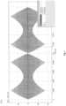
- Fig. 6the circulating current I and an average of the circulating current I is depicted over time for a regular power supply, as shown in Fig. 1 . It can clearly be seen that the average circulating current has values up to 16A.
- Fig. 7the circulating current and the average circulating current of a power supply according to the first aspect of the invention, as shown in Fig. 3 is depicted.
- the average circulating currenthas a maximum value of lower than 0,5A. This constitutes a significant reduction in circulating current and therefore in a significant increase in the efficiency of the coupling by the coupling inductor 13.
- Fig. 8an embodiment of the method according to the second aspect of the invention is shown.
- an AC-input signalis rectified in order to generate a DC-bus voltage.
- a first pulse width modulation signalis generated.
- a phase shift by 180° of a signal, the first pulse width modulation signal is derived from,is performed.
- This signalis the first pulse width modulation control signal PWM1CTRL from Fig.3 .
- PWM1CTRLthe first pulse width modulation control signal
- a second pulse width modulation signalis generated from the provisional second pulse width modulation signal. This is done by increasing the duty cycle of the provisional second pulse width modulation signal as explained earlier.
- the compensation signal Yis added to the duty cycle of the provisional second pulse width modulation signal.
- the first pulse width modulation signal and the second pulse width modulation signalare combined in a coupled inductor, resulting in an output signal.
- the inventionis not limited to the examples and especially not to the displayed type of inverter. Also the invention can be applied to power supplies having more than two converter legs. The characteristics of the exemplary embodiments can be used in any advantageous combination.
Landscapes
- Engineering & Computer Science (AREA)
- Power Engineering (AREA)
- Inverter Devices (AREA)
- Dc-Dc Converters (AREA)
Description
- The invention relates to switched power supplies.
- In switched power supplies, an increased efficiency and reduced hardware cost can be achieved by using more than one switching leg. When combining the signals generated by the more than one switching legs in a coupled inductor, circulation currents can arise. These circulation currents lead to a magnetic saturation of the coupled inductor and thereby to coupling losses. It is therefore important to prevent such circulation currents within the coupled inductor.
- One exemplary solution to this problem is to provide a hall current transducer in each switching leg in order to measure the current in each switching leg. By this method, it is possible to determine the presence of circulation current and to counteract it. This method though is disadvantageous, since hall current transducers are rather expensive components.
- Miller S K T et al: "A Comprehensive Study of Harmonic Cancellation Effects in Interleaved Three-Phase VSCs", XP031218263 discloses interleaving on three-phase voltage-sourced converters including analyzing circulating current among parallel modules.Wang Zhan et al: "Paralleling GaN HEMTs for diode-free bridge power converters", XP032775379 discloses high electron mobility transistors paralleled for diode-free bridge power converters, including a GaN device driver design and application of a partial phase method for low power applications.
WO 2015/000291 A1 discloses a multi-level inverter and a power supply system corresponding to the preamble ofclaim 1 and, in particular, comprising two T-type inverter units linked by coupled inductors and wherein the pulse width modulation waves of the two inverter units are staggered by a phase of 180 degrees. - The object of the invention therefore is to provide a power supply and a method for generating an output signal, which achieve a high efficiency, while at the same time keeping the hardware costs to a minimum.
- The object is solved by the features of
claim 1 for the apparatus and claim 6 for the method. The dependent claims contain further developments. - According to a first aspect of the invention, a power supply for generating an output signal is provided. The power supply comprises:
- a pulse width modulator, adapted to generate a first pulse width modulation control signal with a modulation wave signal m(n). w herein n is a time index,
- a first inverter leg, adapted to generate a first pulse width modulation signal by modulating an input DC voltage from the generated first pulse width modulation control signal,
- a second inverter leg, adapted to generate a second pulse width modulation signal by modulating the input DC voltage from a generated second pulse width modulation control signal,
- a phase shifter, adapted to generate a provisional second pulse width modulation signal by phase shifting the first pulse width modulation control signal,
- a compensator, adapted to determine the second pulse width modulation control signal from the provisional second pulse width modulation control signal, by adding a compensation signal, wherein the compensation signal is determined dependent upon the modulation wave signal m(n), and
- a coupled inductor adapted to combine the first pulse width modulation signal and the second pulse width modulation signal to form the output signal,
- By using the compensation signal, it is possible to compensate circulation current within the coupled inductor. The magnetic saturation is kept at a minimum, which maximizes the efficiency of the power supply.
- The modulation wave signal m(n) may be an AC signal. An especially simple modulation can thereby be achieved.
- The compensator may be adapted to determine the compensation signal Y limited by a pre-specified maximum value. A continuous operation of the power supply is thereby assured.
- The power supply may moreover comprise a rectifier, which is adapted to generate a DC-bus voltage by rectifying an AC-input voltage. It is thereby possible to very flexibly use the power supply on a mains line.
- The phase shifter may be adapted to generate the provisional second pulse width modulation signal with an identical duty cycle as the first pulse width modulation signal. It is thereby possible to very simply generate the provisional second pulse width modulation signal.
- According to a second aspect of the invention, a method for generating an output signal is provided. The method comprises the following steps:
- generating a first pulse width modulation control signal, with a modulation wave signal m(n), wherein n is a time index,
- generating a first pulse width modulation signal by modulating an input DC voltage from the generated first pulse width modulation control signal, generating a second pulse width modulation control signal by modulating an input DC voltage from a generated second pulse width modulation control signal,
- determining a provisional second pulse width modulation control signal by phase shifting the first pulse width modulation control signal,
- determining the second pulse width modulation control signal from the provisional second pulse width modulation signal, by adding a compensation signal, wherein the compensation signal is determined dependent upon the modulation wave signal m(n), and
- combining the first pulse width modulation signal and the second pulse width modulation control signal through a coupled inductor to form the output signal,
- The modulation wave signal may be an AC signal. An especially simple modulation can thereby be achieved.
- The compensation signal Y may be determined limited by a pre-specified maximum value. A continuous operation of the power supply is thereby assured.
- The method may further comprise generating a DC-bus voltage by rectifying an AC-input voltage. It is thereby possible to very flexibly use the power supply on a mains line.
- The provisional second pulse width modulation signal may be generated with an identical duty cycle as the first pulse width modulation signal. It is thereby possible to very simply generate the provisional second pulse width modulation signal.
- Generally, it has to be noted that all arrangements, devices, elements, units and means and so forth described in the present application could be implemented by software or hardware elements or any kind of combination thereof. Furthermore, the devices may be processors or may comprise processors, wherein the functions of the elements, units and means described in the present applications may be implemented in one or more processors. All steps which are performed by the various entities described in the present application as well as the functionality described to be performed by the various entities are intended to mean that the respective entity is adapted to or configured to perform the respective steps and functionalities. Even if in the following description or specific embodiments, a specific functionality or step to be performed by a general entity is not reflected in the description of a specific detailed element of that entity which performs that specific step or functionality, it should be clear for a skilled person that these methods and functionalities can be implemented in respect of software or hardware elements, or any kind of combination thereof.
- The present invention is in the following explained in detail in relation to embodiments of the invention in reference to the enclosed drawings, in which:
- Fig. 1
- shows a first exemplary power supply;
- Fig. 2
- shows different signals in an exemplary power supply;
- Fig. 3
- shows a first embodiment of the power supply according to the first aspect of the invention in a block diagram;
- Fig. 4
- shows an exemplary modulation wave signal;
- Fig. 5
- shows different signals in a second embodiment of the power supply according to the first aspect of the invention;
- Fig. 6
- shows resulting signals;
- Fig. 7
- shows exemplary output signals of a third embodiment of the power supply according to the first aspect of the invention, and
- Fig. 8
- shows an embodiment of the method according to the second aspect of the invention as a flow diagram.
- First we demonstrate the construction of a switching power supply along
Fig. 1 . With regard toFig. 2 , the problem of circulation current is further explained. With regard toFigs. 3-5 , the construction and function of different embodiments of the power supply according to the first aspect of the invention is described. With regard toFig. 6 andFig. 7 , achievable results by use of the invention are shown. Finally, alongFig. 8 , the function of an embodiment of the method according to the second aspect of the invention is illustrated. Similar entities and reference numbers in different figures have been partially omitted. - In
Fig. 1 , anexemplary power supply 1 is shown. Thepower supply 1 comprises aninverter 2 which has apositive voltage rail 31, anegative voltage rail 32, and a number of switches 21 - 28. The switches 21 - 28 are put into practice as a parallel connection of a transistor and a diode, each. Moreover, thepositive voltage rail 31 is connected through acapacitance 29 to aground connection 33. Also thenegative voltage rail 32 is connected through acapacitance 30 to theground connection 33. Theinverter 2 is connected to a coupledinductor 13. An output terminal of the coupledinductor 13 is fed through a hallcurrent transducer 38 and connected to acapacitance 36 and aresistance 37. Thecapacitance 36 is connected to aground connection 34. Theresistance 37 is connected to aground connection 35. - For operating the
power supply 1, a DC-input voltage is supplied between thepositive voltage rail 31 and thenegative voltage rail 32. The switches 21 - 28 are switched so that a first pulse width modulation signal PWM1 and a second pulse width modulation signal PWM2 are generated and supplied to two separate inputs of the coupledinductor 13. The coupledinductor 13 combines the two signals forming and output current iL. This current is measured by the hallcurrent transducer 38. - The first pulse width modulation signal PWM1 and the second pulse width modulation signal PWM2 are generated by the switches 21 - 28 by modulating the input signal with a modulation wave signal. Such a modulation wave signal is for example shown in
Fig. 4 . The resulting signals are 180° phase shifted. With the set up shown here, it is difficult to ensure a volt-second balance between the coupled legs. This can lead to circulation current within the coupledinductor 13. This circulation current drives the magnetic field within the coupled inductor into saturation leading to a reduced coupling efficiency and thereby to a reduced efficiency of theoverall power supply 1. - As explained earlier, this problem can be solved by adding a further hall current transducer for measuring i1 and i2, but this requires great additional effort. Also, this requires a high control frequency of the control loop for reducing the circulation current.
- In
Fig. 2 , a first exemplary pulse width modulation signal PWM1 and a second exemplary pulse width modulation signal PWM2 are depicted. Above these signals, the resulting circulation currents are shown. The circulating current is the difference between the current on the first inverter leg and the current on the second inverter leg. As one can easily see, there remains an average circulating current, which drives the magnetic field within the coupledinductor 13 into saturation. Without additional sensors, this cannot be prevented using only the measures shown inFig. 1 . It is not possible to perform a closed loop regulation of the circulating current, since the respective sensors are not present. - The power supply according to
Fig. 1 though can be expanded to a power supply according to the first aspect of the present invention. Such apower supply 1 is shown inFig. 3 . There, thepower supply 1 is shown in a block diagram. Arectifier 10 is connected to aninverter 2, which is moreover connected to a coupledinductor 13. The inverter especially comprises afirst inverter leg 11 and asecond inverter leg 12. Only thefirst inverter leg 11 though operates a conventional pulse width modulator. Thefirst inverter leg 11 comprises a pulse widthmodulation determining unit 110, which is connected to apulse width modulator 112, which in turn is connected to afirst switch 111. - The
second inverter leg 12 on the other hand comprises aphase shifter 120 connected to acompensator 121, which again is connected to asecond switch 122. Thefirst inverter leg 11, especially thefirst switch 111 is connected to a first leg of the coupledinductor 13. Thesecond inverter leg 12, especially thesecond switch 122 is connected to a second leg of the coupledinductor 13. It is important to mention, that thefirst switch 111 and thesecond switch 122 can be constructed as a plurality of transistors, as shown inFig. 1 . - When operating the
power supply 1, an AC-input signal ACIN is provided to therectifier 10. Therectifier 10 rectifies the AC-input signal ACIN generating a DC-input signal IN. This input signal IN is provided to thefirst switch 111 and to thesecond switch 122. - The pulse width
modulation determining unit 110 generates a modulation wave signal MWS and supplies it to thepulse width modulator 112. A carrier signal, preferably a triangle signal is moreover provided to the pulse width modulator. The modulator compares the modulation wave signal MWS to the carrier signal. When the modulation wave signal MWS is larger than the carrier signal, the modulator activates thefirst switch 111. When the modulation wave signal MWS is smaller than the carrier signal, the modulator deactivates thefirst switch 111. The resulting signal of the pulse width modulator therefore is a first pulse width modulation control signal PWM2CTRL. This signal activates and deactivates thefirst switch 111. - The
first switch 111 therefore modulates the input signal IN based on the modulation wave signal MWS. A first pulse width modulation signal PWM1 results. - This first pulse width modulation control signal signalPWMICTRL is handed to the
phase shifter 120, which generates a provisional second pulse width modulation signal PWM2' by phase shifting the first pulsewidth modulation signal 1 by 180°. The provisional second pulse width modulation signal PWM2' is handed to thecompensator 121, which performs a compensation of circulating current within the coupledinductor 13. For this purpose, thecompensator 121 adds a compensation signal Y to the provisional second pulse width modulation signal. Especially, this is done by increasing the duty cycle of the provisional second pulse width modulation signal PWM2' by a value Y. This is further shown alongFig. 5 . The resulting second pulse width modulation control signal PWM2CTRL is provided to thesecond switch 122, which modulates the input signal IN using the second pulse width modulation control signal PWM2CTRL. As a result, thesecond switch 122 generates a second pulse width modulation signal PWM2. The coupledinductor 13 combines the first pulse width modulation signal PWM1 and the second pulse width modulation signal PWM2. This results in the output signal OUT. - Although there is no closed loop control regarding the circulating current within the coupled
inductor 13, the above-shown measure still significantly reduces the circulating current, since systematic error within the pulse width modulation signals are corrected. InFig. 4 , an exemplary modulation wave signal is shown over time. Here different values of the modulation wave signal at different instances in time are depicted. - In
Fig. 5 , the different signals within thepower supply 1 ofFig. 3 are shown. The first pulse width modulation signal PWM1 has a certain pulse width. The provisional second pulse width modulation signal PWM2' has the identical pulse width and therefore the identical duty cycle as the first pulse width modulation signal PWM1, but it is phase shifted by 180°. The second pulse width modulation signal PWM2 is still phase shifted by 180° with regard to the first pulse width modulation signal PWM1, but the duty cycle is amended by adding the value Y. This is shown inFig. 5 . In the present invention, the value Y must be determined as:
- This calculation is based upon a linear approximation. Alternatively, also a more accurate approximation can be used.
- In
Fig. 6 , the circulating current I and an average of the circulating current I is depicted over time for a regular power supply, as shown inFig. 1 . It can clearly be seen that the average circulating current has values up to 16A. - In
Fig. 7 , the circulating current and the average circulating current of a power supply according to the first aspect of the invention, as shown inFig. 3 is depicted. Here it can clearly be seen that the average circulating current has a maximum value of lower than 0,5A. This constitutes a significant reduction in circulating current and therefore in a significant increase in the efficiency of the coupling by thecoupling inductor 13. Finally, inFig. 8 , an embodiment of the method according to the second aspect of the invention is shown. In an optionalfirst step 100, an AC-input signal is rectified in order to generate a DC-bus voltage. In asecond step 101, a first pulse width modulation signal is generated. In athird step 102, a phase shift by 180° of a signal, the first pulse width modulation signal is derived from, is performed. This signal is the first pulse width modulation control signal PWM1CTRL fromFig.3 . This results in a provisional second pulse width modulation signal. In afourth step 103, a second pulse width modulation signal is generated from the provisional second pulse width modulation signal. This is done by increasing the duty cycle of the provisional second pulse width modulation signal as explained earlier. The compensation signal Y is added to the duty cycle of the provisional second pulse width modulation signal. In a finalfifth step 104 the first pulse width modulation signal and the second pulse width modulation signal are combined in a coupled inductor, resulting in an output signal. - The invention is not limited to the examples and especially not to the displayed type of inverter. Also the invention can be applied to power supplies having more than two converter legs. The characteristics of the exemplary embodiments can be used in any advantageous combination.
- The invention has been described in conjunction with various embodiments herein. However, other variations to the disclosed embodiments can be understood and effected by those skilled in the art in practicing the claimed invention, from a study of the drawings, the disclosure and the appended claims, said variations being considered part of the present invention insofar as they do not contradict the appended claims (i.e. if they comprise all features of at least one of the appended
independent claims 1 and 6). - In the claims, the word "comprising "does not exclude other elements or steps and the indefinite article "a" or "an" does not exclude a plurality. A single processor or other unit may fulfill the functions of several items recited in the claims. The mere fact that certain measures are recited in usually different dependent claims does not indicate that a combination of these measures cannot be used to advantage. A computer program may be stored/distributed on a suitable medium, such as an optical storage medium or a solid-state medium supplied together with or as part of other hardware, but may also be distributed in other forms, such as via the internet or other wired or wireless communication systems.

Claims (9)
- A power supply (1) for generating an output signal, comprising:- a pulse width modulator, adapted to generate a first pulse width modulation control signal with a modulation wave signal m(n), wherein n is a time index,- a first inverter leg (11), adapted to generate a first pulse width modulation signal by modulating an input DC voltage from the first pulse width modulation control signal,- a second inverter leg (12), adapted to generate a second pulse width modulation signal by modulating the input DC voltage from a second pulse width modulation control signal,- a phase shifter, adapted to generate a provisional second pulse width modulation signal by phase shifting the first pulse width modulation control signal,- a compensator (121), adapted to determine the second pulse width modulation control signal from the provisional second pulse width modulation signal, by adding a compensation signal, wherein the compensation signal is determined dependent upon the modulation wave signal m(n), and- a coupled inductor (13), adapted to combine the first pulse width modulation signal and the second pulse width modulation signal to form the output signal, wherein the compensator is adapted to determine the second pulse width modulation control signal in order to compensate for a circulation current within the coupled inductor,characterized in that the compensator (121) is adapted to determine the compensation signal as:

- The power supply (1) of claim 1, wherein the modulation wave signal m(n) is an AC signal.
- The power supply (1) of claim 1, wherein the compensator (121) is adapted to determine the compensation signal Y limited by a pre-specified maximum value.
- The power supply (1) of any of claims 1 to 3, comprising a rectifier (10), adapted to generate the DC input voltage by rectifying an AC input voltage.
- The power supply of any of claims 1 to 4, wherein the phase shifter (120) is adapted to generate the provisional second pulse width modulation signal with an identical duty cycle as the first pulse width modulation signal.
- A method for generating an output signal, comprising the following steps:- generating a first pulse width modulation control signal, with a modulation wave signal m(n), wherein n is a time index,- generating (101), at a first inverter leg (11), a first pulse width modulation signal by modulating an input DC voltage from the first pulse width modulation control signal,- generating (103), at a second inverter leg (12), a second pulse width modulation signal by modulating the input DC voltage from a second pulse width modulation control signal,- determining a provisional second pulse width modulation signal by phase shifting the first pulse width modulation control signal,- determining the second pulse width modulation control signal from the provisional second pulse width modulation signal, by adding a compensation signal, wherein the compensation signal is determined dependent upon the modulation wave signal m(n), and- combining (104) the first pulse width modulation signal and the second pulse width modulation signal through a coupled inductor to form the output signal, wherein the compensation signal is determined in order to compensate for a circulation current within the coupled inductor,characterized in that the compensation signal is determined as: Y = 2 × Δm, wherein Y is the compensation signal, and wherein Δm is determined as m(n) - m(n-1).
- The method of claim 6, wherein the modulation wave signal m(n) is an AC signal.
- The method of claim 6, wherein compensation signal Y is determined limited by a pre-specified maximum value.
- The method of any of claims 6 and 7, comprising generating the DC input voltage by rectifying an AC input voltage.

Applications Claiming Priority (1)
| Application Number | Priority Date | Filing Date | Title |
|---|---|---|---|
| PCT/EP2017/051370WO2018137752A1 (en) | 2017-01-24 | 2017-01-24 | Power supply and power supply method with circulation current compensation |
Publications (2)
| Publication Number | Publication Date |
|---|---|
| EP3566290A1 EP3566290A1 (en) | 2019-11-13 |
| EP3566290B1true EP3566290B1 (en) | 2023-04-05 |
Family
ID=58044009
Family Applications (1)
| Application Number | Title | Priority Date | Filing Date |
|---|---|---|---|
| EP17705021.8AActiveEP3566290B1 (en) | 2017-01-24 | 2017-01-24 | Power supply and power supply method with circulation current compensation |
Country Status (4)
| Country | Link |
|---|---|
| US (1) | US10826413B2 (en) |
| EP (1) | EP3566290B1 (en) |
| CN (1) | CN110168882B (en) |
| WO (1) | WO2018137752A1 (en) |
Citations (1)
| Publication number | Priority date | Publication date | Assignee | Title |
|---|---|---|---|---|
| WO2015000291A1 (en)* | 2013-07-05 | 2015-01-08 | 华为技术有限公司 | Multi-level inverter and power supply system |
Family Cites Families (14)
| Publication number | Priority date | Publication date | Assignee | Title |
|---|---|---|---|---|
| US5808453A (en) | 1996-08-21 | 1998-09-15 | Siliconix Incorporated | Synchronous current sharing pulse width modulator |
| TW546897B (en)* | 2001-08-31 | 2003-08-11 | Delta Electronics Inc | Electronic circuit apparatus having suppression of harmonics and voltage stabilization function and control method |
| DE10213296B9 (en)* | 2002-03-25 | 2007-04-19 | Infineon Technologies Ag | Electronic component with a semiconductor chip, method for its production and method for producing a benefit |
| US6642683B1 (en)* | 2002-08-26 | 2003-11-04 | The Boeing Company | Controller and associated drive assembly for power sharing, time sliced control of a brushless direct current motor |
| US6727605B1 (en) | 2002-10-09 | 2004-04-27 | Delphi Technologies, Inc. | Duty cycle phase number control of polyphase interleaved converters |
| US8089256B2 (en) | 2008-10-10 | 2012-01-03 | Powervation Ltd. | Multiphase switching converter |
| JP2011072167A (en)* | 2009-09-28 | 2011-04-07 | Tdk-Lambda Corp | Controller, control method, and program |
| TWI474606B (en)* | 2011-09-08 | 2015-02-21 | Delta Electronics Inc | Parallel inverter drive system and the apparatus and method for suppressing circulating current in such system |
| US8896182B2 (en)* | 2012-04-05 | 2014-11-25 | General Electric Corporation | System for driving a piezoelectric load and method of making same |
| US8964432B2 (en)* | 2013-01-29 | 2015-02-24 | The Boeing Company | Apparatus and method for controlling circulating current in an inverter system |
| CN104836209B (en) | 2015-04-30 | 2018-01-23 | 华为技术有限公司 | A kind of digital power protection circuit and device |
| FR3048139B1 (en)* | 2016-02-18 | 2018-01-26 | Schneider Toshiba Inverter Europe Sas | METHOD AND CONTROL SYSTEM FOR AN ELECTRIC MOTOR CONTROL INSTALLATION |
| FR3058590B1 (en)* | 2016-11-07 | 2019-06-21 | Ge Energy Power Conversion Technology Limited | METHOD FOR CONTROLLING ASYNCHRONOUS IMPULSE WIDTH MODULATION OF AT LEAST TWO THREE PHASE POWER CONVERTERS. |
| US10050531B1 (en)* | 2017-01-24 | 2018-08-14 | General Electric Company | Direct flux control power converter |
- 2017
- 2017-01-24CNCN201780080272.9Apatent/CN110168882B/enactiveActive
- 2017-01-24EPEP17705021.8Apatent/EP3566290B1/enactiveActive
- 2017-01-24WOPCT/EP2017/051370patent/WO2018137752A1/ennot_activeCeased
- 2019
- 2019-07-24USUS16/521,195patent/US10826413B2/enactiveActive
Patent Citations (1)
| Publication number | Priority date | Publication date | Assignee | Title |
|---|---|---|---|---|
| WO2015000291A1 (en)* | 2013-07-05 | 2015-01-08 | 华为技术有限公司 | Multi-level inverter and power supply system |
Also Published As
| Publication number | Publication date |
|---|---|
| EP3566290A1 (en) | 2019-11-13 |
| US10826413B2 (en) | 2020-11-03 |
| US20190356241A1 (en) | 2019-11-21 |
| WO2018137752A1 (en) | 2018-08-02 |
| CN110168882B (en) | 2021-11-19 |
| CN110168882A (en) | 2019-08-23 |
Similar Documents
| Publication | Publication Date | Title |
|---|---|---|
| US10148136B2 (en) | Drive device, method thereof, and wireless power transmission device | |
| EP2568589B1 (en) | Multilevel converter comprising an active AC-DC converter and a resonant DC-DC converter and a control method for operating a multilevel converter | |
| US10338172B2 (en) | Power device and method for driving a load | |
| JP6357976B2 (en) | DC power supply | |
| JP2019525700A (en) | High frequency high power converter system | |
| US9979311B2 (en) | Matrix converter | |
| US8559194B2 (en) | Converter circuit and unit and system comprising such converter circuit | |
| CN102396142A (en) | Method of controlling power conversion device | |
| US9036373B2 (en) | Closed loop control of a cyclo-converter | |
| JP6948938B2 (en) | DC converter | |
| JPWO2017131096A1 (en) | Power converter | |
| JP2013005589A (en) | Power converter and control method of power converter | |
| CN105610173B (en) | Digit power factor correction | |
| Yamanodera et al. | Application of GaN device to MHz operating grid-tied inverter using discontinuous current mode for compact and efficient power conversion | |
| TWI388116B (en) | Method and device for active phase-to-phase transformer used in twenty-four pulse wave AC / DC converter | |
| EP3566290B1 (en) | Power supply and power supply method with circulation current compensation | |
| EP1811643A1 (en) | Power converter | |
| AU2018392788B2 (en) | Three-phase AC/AC converter with quasi-sine wave HF series resonant link | |
| JP2010246371A (en) | Method for operating converter circuit, and apparatus for carrying out the method | |
| Babenko et al. | Energy and noise characteristics of a SEPIC/CUK converter with bipolar output | |
| WO2011058665A1 (en) | Power conversion device | |
| JP2017005841A (en) | Power transmission apparatus | |
| NO323385B1 (en) | Control method and device for inverters using a TSSC | |
| EP3024133A1 (en) | DC-to-AC power converter | |
| Oliveira et al. | A bidirectional Single-stage three-phase AC/DC converter with high-frequency isolation and PFC |
Legal Events
| Date | Code | Title | Description |
|---|---|---|---|
| STAA | Information on the status of an ep patent application or granted ep patent | Free format text:STATUS: UNKNOWN | |
| STAA | Information on the status of an ep patent application or granted ep patent | Free format text:STATUS: THE INTERNATIONAL PUBLICATION HAS BEEN MADE | |
| PUAI | Public reference made under article 153(3) epc to a published international application that has entered the european phase | Free format text:ORIGINAL CODE: 0009012 | |
| STAA | Information on the status of an ep patent application or granted ep patent | Free format text:STATUS: REQUEST FOR EXAMINATION WAS MADE | |
| 17P | Request for examination filed | Effective date:20190808 | |
| AK | Designated contracting states | Kind code of ref document:A1 Designated state(s):AL AT BE BG CH CY CZ DE DK EE ES FI FR GB GR HR HU IE IS IT LI LT LU LV MC MK MT NL NO PL PT RO RS SE SI SK SM TR | |
| AX | Request for extension of the european patent | Extension state:BA ME | |
| DAV | Request for validation of the european patent (deleted) | ||
| DAX | Request for extension of the european patent (deleted) | ||
| STAA | Information on the status of an ep patent application or granted ep patent | Free format text:STATUS: EXAMINATION IS IN PROGRESS | |
| RAP1 | Party data changed (applicant data changed or rights of an application transferred) | Owner name:HUAWEI DIGITAL POWER TECHNOLOGIES CO., LTD. | |
| 17Q | First examination report despatched | Effective date:20211206 | |
| GRAP | Despatch of communication of intention to grant a patent | Free format text:ORIGINAL CODE: EPIDOSNIGR1 | |
| STAA | Information on the status of an ep patent application or granted ep patent | Free format text:STATUS: GRANT OF PATENT IS INTENDED | |
| INTG | Intention to grant announced | Effective date:20221128 | |
| GRAS | Grant fee paid | Free format text:ORIGINAL CODE: EPIDOSNIGR3 | |
| GRAA | (expected) grant | Free format text:ORIGINAL CODE: 0009210 | |
| STAA | Information on the status of an ep patent application or granted ep patent | Free format text:STATUS: THE PATENT HAS BEEN GRANTED | |
| AK | Designated contracting states | Kind code of ref document:B1 Designated state(s):AL AT BE BG CH CY CZ DE DK EE ES FI FR GB GR HR HU IE IS IT LI LT LU LV MC MK MT NL NO PL PT RO RS SE SI SK SM TR | |
| REG | Reference to a national code | Ref country code:GB Ref legal event code:FG4D | |
| REG | Reference to a national code | Ref country code:CH Ref legal event code:EP | |
| REG | Reference to a national code | Ref country code:AT Ref legal event code:REF Ref document number:1559001 Country of ref document:AT Kind code of ref document:T Effective date:20230415 | |
| REG | Reference to a national code | Ref country code:DE Ref legal event code:R096 Ref document number:602017067404 Country of ref document:DE | |
| REG | Reference to a national code | Ref country code:IE Ref legal event code:FG4D | |
| P01 | Opt-out of the competence of the unified patent court (upc) registered | Effective date:20230524 | |
| REG | Reference to a national code | Ref country code:LT Ref legal event code:MG9D | |
| REG | Reference to a national code | Ref country code:NL Ref legal event code:MP Effective date:20230405 | |
| REG | Reference to a national code | Ref country code:AT Ref legal event code:MK05 Ref document number:1559001 Country of ref document:AT Kind code of ref document:T Effective date:20230405 | |
| PG25 | Lapsed in a contracting state [announced via postgrant information from national office to epo] | Ref country code:NL Free format text:LAPSE BECAUSE OF FAILURE TO SUBMIT A TRANSLATION OF THE DESCRIPTION OR TO PAY THE FEE WITHIN THE PRESCRIBED TIME-LIMIT Effective date:20230405 | |
| PG25 | Lapsed in a contracting state [announced via postgrant information from national office to epo] | Ref country code:SE Free format text:LAPSE BECAUSE OF FAILURE TO SUBMIT A TRANSLATION OF THE DESCRIPTION OR TO PAY THE FEE WITHIN THE PRESCRIBED TIME-LIMIT Effective date:20230405 Ref country code:PT Free format text:LAPSE BECAUSE OF FAILURE TO SUBMIT A TRANSLATION OF THE DESCRIPTION OR TO PAY THE FEE WITHIN THE PRESCRIBED TIME-LIMIT Effective date:20230807 Ref country code:NO Free format text:LAPSE BECAUSE OF FAILURE TO SUBMIT A TRANSLATION OF THE DESCRIPTION OR TO PAY THE FEE WITHIN THE PRESCRIBED TIME-LIMIT Effective date:20230705 Ref country code:ES Free format text:LAPSE BECAUSE OF FAILURE TO SUBMIT A TRANSLATION OF THE DESCRIPTION OR TO PAY THE FEE WITHIN THE PRESCRIBED TIME-LIMIT Effective date:20230405 Ref country code:AT Free format text:LAPSE BECAUSE OF FAILURE TO SUBMIT A TRANSLATION OF THE DESCRIPTION OR TO PAY THE FEE WITHIN THE PRESCRIBED TIME-LIMIT Effective date:20230405 | |
| PG25 | Lapsed in a contracting state [announced via postgrant information from national office to epo] | Ref country code:RS Free format text:LAPSE BECAUSE OF FAILURE TO SUBMIT A TRANSLATION OF THE DESCRIPTION OR TO PAY THE FEE WITHIN THE PRESCRIBED TIME-LIMIT Effective date:20230405 Ref country code:PL Free format text:LAPSE BECAUSE OF FAILURE TO SUBMIT A TRANSLATION OF THE DESCRIPTION OR TO PAY THE FEE WITHIN THE PRESCRIBED TIME-LIMIT Effective date:20230405 Ref country code:LV Free format text:LAPSE BECAUSE OF FAILURE TO SUBMIT A TRANSLATION OF THE DESCRIPTION OR TO PAY THE FEE WITHIN THE PRESCRIBED TIME-LIMIT Effective date:20230405 Ref country code:LT Free format text:LAPSE BECAUSE OF FAILURE TO SUBMIT A TRANSLATION OF THE DESCRIPTION OR TO PAY THE FEE WITHIN THE PRESCRIBED TIME-LIMIT Effective date:20230405 Ref country code:IS Free format text:LAPSE BECAUSE OF FAILURE TO SUBMIT A TRANSLATION OF THE DESCRIPTION OR TO PAY THE FEE WITHIN THE PRESCRIBED TIME-LIMIT Effective date:20230805 Ref country code:HR Free format text:LAPSE BECAUSE OF FAILURE TO SUBMIT A TRANSLATION OF THE DESCRIPTION OR TO PAY THE FEE WITHIN THE PRESCRIBED TIME-LIMIT Effective date:20230405 Ref country code:GR Free format text:LAPSE BECAUSE OF FAILURE TO SUBMIT A TRANSLATION OF THE DESCRIPTION OR TO PAY THE FEE WITHIN THE PRESCRIBED TIME-LIMIT Effective date:20230706 Ref country code:AL Free format text:LAPSE BECAUSE OF FAILURE TO SUBMIT A TRANSLATION OF THE DESCRIPTION OR TO PAY THE FEE WITHIN THE PRESCRIBED TIME-LIMIT Effective date:20230405 | |
| PG25 | Lapsed in a contracting state [announced via postgrant information from national office to epo] | Ref country code:FI Free format text:LAPSE BECAUSE OF FAILURE TO SUBMIT A TRANSLATION OF THE DESCRIPTION OR TO PAY THE FEE WITHIN THE PRESCRIBED TIME-LIMIT Effective date:20230405 | |
| REG | Reference to a national code | Ref country code:DE Ref legal event code:R097 Ref document number:602017067404 Country of ref document:DE | |
| PG25 | Lapsed in a contracting state [announced via postgrant information from national office to epo] | Ref country code:SK Free format text:LAPSE BECAUSE OF FAILURE TO SUBMIT A TRANSLATION OF THE DESCRIPTION OR TO PAY THE FEE WITHIN THE PRESCRIBED TIME-LIMIT Effective date:20230405 | |
| PG25 | Lapsed in a contracting state [announced via postgrant information from national office to epo] | Ref country code:SM Free format text:LAPSE BECAUSE OF FAILURE TO SUBMIT A TRANSLATION OF THE DESCRIPTION OR TO PAY THE FEE WITHIN THE PRESCRIBED TIME-LIMIT Effective date:20230405 Ref country code:SK Free format text:LAPSE BECAUSE OF FAILURE TO SUBMIT A TRANSLATION OF THE DESCRIPTION OR TO PAY THE FEE WITHIN THE PRESCRIBED TIME-LIMIT Effective date:20230405 Ref country code:RO Free format text:LAPSE BECAUSE OF FAILURE TO SUBMIT A TRANSLATION OF THE DESCRIPTION OR TO PAY THE FEE WITHIN THE PRESCRIBED TIME-LIMIT Effective date:20230405 Ref country code:EE Free format text:LAPSE BECAUSE OF FAILURE TO SUBMIT A TRANSLATION OF THE DESCRIPTION OR TO PAY THE FEE WITHIN THE PRESCRIBED TIME-LIMIT Effective date:20230405 Ref country code:DK Free format text:LAPSE BECAUSE OF FAILURE TO SUBMIT A TRANSLATION OF THE DESCRIPTION OR TO PAY THE FEE WITHIN THE PRESCRIBED TIME-LIMIT Effective date:20230405 Ref country code:CZ Free format text:LAPSE BECAUSE OF FAILURE TO SUBMIT A TRANSLATION OF THE DESCRIPTION OR TO PAY THE FEE WITHIN THE PRESCRIBED TIME-LIMIT Effective date:20230405 | |
| PLBE | No opposition filed within time limit | Free format text:ORIGINAL CODE: 0009261 | |
| STAA | Information on the status of an ep patent application or granted ep patent | Free format text:STATUS: NO OPPOSITION FILED WITHIN TIME LIMIT | |
| 26N | No opposition filed | Effective date:20240108 | |
| PG25 | Lapsed in a contracting state [announced via postgrant information from national office to epo] | Ref country code:SI Free format text:LAPSE BECAUSE OF FAILURE TO SUBMIT A TRANSLATION OF THE DESCRIPTION OR TO PAY THE FEE WITHIN THE PRESCRIBED TIME-LIMIT Effective date:20230405 | |
| PG25 | Lapsed in a contracting state [announced via postgrant information from national office to epo] | Ref country code:SI Free format text:LAPSE BECAUSE OF FAILURE TO SUBMIT A TRANSLATION OF THE DESCRIPTION OR TO PAY THE FEE WITHIN THE PRESCRIBED TIME-LIMIT Effective date:20230405 Ref country code:IT Free format text:LAPSE BECAUSE OF FAILURE TO SUBMIT A TRANSLATION OF THE DESCRIPTION OR TO PAY THE FEE WITHIN THE PRESCRIBED TIME-LIMIT Effective date:20230405 | |
| PG25 | Lapsed in a contracting state [announced via postgrant information from national office to epo] | Ref country code:MC Free format text:LAPSE BECAUSE OF FAILURE TO SUBMIT A TRANSLATION OF THE DESCRIPTION OR TO PAY THE FEE WITHIN THE PRESCRIBED TIME-LIMIT Effective date:20230405 | |
| PG25 | Lapsed in a contracting state [announced via postgrant information from national office to epo] | Ref country code:MC Free format text:LAPSE BECAUSE OF FAILURE TO SUBMIT A TRANSLATION OF THE DESCRIPTION OR TO PAY THE FEE WITHIN THE PRESCRIBED TIME-LIMIT Effective date:20230405 | |
| REG | Reference to a national code | Ref country code:CH Ref legal event code:PL | |
| PG25 | Lapsed in a contracting state [announced via postgrant information from national office to epo] | Ref country code:LU Free format text:LAPSE BECAUSE OF NON-PAYMENT OF DUE FEES Effective date:20240124 | |
| GBPC | Gb: european patent ceased through non-payment of renewal fee | Effective date:20240124 | |
| PG25 | Lapsed in a contracting state [announced via postgrant information from national office to epo] | Ref country code:LU Free format text:LAPSE BECAUSE OF NON-PAYMENT OF DUE FEES Effective date:20240124 | |
| PG25 | Lapsed in a contracting state [announced via postgrant information from national office to epo] | Ref country code:GB Free format text:LAPSE BECAUSE OF NON-PAYMENT OF DUE FEES Effective date:20240124 | |
| PG25 | Lapsed in a contracting state [announced via postgrant information from national office to epo] | Ref country code:BE Free format text:LAPSE BECAUSE OF NON-PAYMENT OF DUE FEES Effective date:20240131 | |
| PG25 | Lapsed in a contracting state [announced via postgrant information from national office to epo] | Ref country code:CH Free format text:LAPSE BECAUSE OF NON-PAYMENT OF DUE FEES Effective date:20240131 | |
| PG25 | Lapsed in a contracting state [announced via postgrant information from national office to epo] | Ref country code:GB Free format text:LAPSE BECAUSE OF NON-PAYMENT OF DUE FEES Effective date:20240124 Ref country code:CH Free format text:LAPSE BECAUSE OF NON-PAYMENT OF DUE FEES Effective date:20240131 Ref country code:BE Free format text:LAPSE BECAUSE OF NON-PAYMENT OF DUE FEES Effective date:20240131 | |
| REG | Reference to a national code | Ref country code:BE Ref legal event code:MM Effective date:20240131 | |
| PG25 | Lapsed in a contracting state [announced via postgrant information from national office to epo] | Ref country code:BG Free format text:LAPSE BECAUSE OF FAILURE TO SUBMIT A TRANSLATION OF THE DESCRIPTION OR TO PAY THE FEE WITHIN THE PRESCRIBED TIME-LIMIT Effective date:20230405 | |
| PG25 | Lapsed in a contracting state [announced via postgrant information from national office to epo] | Ref country code:BG Free format text:LAPSE BECAUSE OF FAILURE TO SUBMIT A TRANSLATION OF THE DESCRIPTION OR TO PAY THE FEE WITHIN THE PRESCRIBED TIME-LIMIT Effective date:20230405 | |
| PGFP | Annual fee paid to national office [announced via postgrant information from national office to epo] | Ref country code:FR Payment date:20241209 Year of fee payment:9 | |
| PG25 | Lapsed in a contracting state [announced via postgrant information from national office to epo] | Ref country code:IE Free format text:LAPSE BECAUSE OF NON-PAYMENT OF DUE FEES Effective date:20240124 | |
| PG25 | Lapsed in a contracting state [announced via postgrant information from national office to epo] | Ref country code:IE Free format text:LAPSE BECAUSE OF NON-PAYMENT OF DUE FEES Effective date:20240124 | |
| PGFP | Annual fee paid to national office [announced via postgrant information from national office to epo] | Ref country code:DE Payment date:20241203 Year of fee payment:9 | |
| PG25 | Lapsed in a contracting state [announced via postgrant information from national office to epo] | Ref country code:CY Free format text:LAPSE BECAUSE OF FAILURE TO SUBMIT A TRANSLATION OF THE DESCRIPTION OR TO PAY THE FEE WITHIN THE PRESCRIBED TIME-LIMIT; INVALID AB INITIO Effective date:20170124 | |
| PG25 | Lapsed in a contracting state [announced via postgrant information from national office to epo] | Ref country code:HU Free format text:LAPSE BECAUSE OF FAILURE TO SUBMIT A TRANSLATION OF THE DESCRIPTION OR TO PAY THE FEE WITHIN THE PRESCRIBED TIME-LIMIT; INVALID AB INITIO Effective date:20170124 |