EP3563902A1 - Microfabricated neurostimulation device - Google Patents
Microfabricated neurostimulation deviceDownload PDFInfo
- Publication number
- EP3563902A1 EP3563902A1EP19174013.3AEP19174013AEP3563902A1EP 3563902 A1EP3563902 A1EP 3563902A1EP 19174013 AEP19174013 AEP 19174013AEP 3563902 A1EP3563902 A1EP 3563902A1
- Authority
- EP
- European Patent Office
- Prior art keywords
- microelectrode
- elements
- microelectrodes
- probe
- neurological
- Prior art date
- Legal status (The legal status is an assumption and is not a legal conclusion. Google has not performed a legal analysis and makes no representation as to the accuracy of the status listed.)
- Granted
Links
Images


Classifications
- A—HUMAN NECESSITIES
- A61—MEDICAL OR VETERINARY SCIENCE; HYGIENE
- A61N—ELECTROTHERAPY; MAGNETOTHERAPY; RADIATION THERAPY; ULTRASOUND THERAPY
- A61N1/00—Electrotherapy; Circuits therefor
- A61N1/02—Details
- A61N1/04—Electrodes
- A61N1/05—Electrodes for implantation or insertion into the body, e.g. heart electrode
- A61N1/0526—Head electrodes
- A61N1/0529—Electrodes for brain stimulation
- A61N1/0534—Electrodes for deep brain stimulation
- A—HUMAN NECESSITIES
- A61—MEDICAL OR VETERINARY SCIENCE; HYGIENE
- A61B—DIAGNOSIS; SURGERY; IDENTIFICATION
- A61B17/00—Surgical instruments, devices or methods
- A61B17/34—Trocars; Puncturing needles
- A—HUMAN NECESSITIES
- A61—MEDICAL OR VETERINARY SCIENCE; HYGIENE
- A61B—DIAGNOSIS; SURGERY; IDENTIFICATION
- A61B5/00—Measuring for diagnostic purposes; Identification of persons
- A61B5/24—Detecting, measuring or recording bioelectric or biomagnetic signals of the body or parts thereof
- A—HUMAN NECESSITIES
- A61—MEDICAL OR VETERINARY SCIENCE; HYGIENE
- A61B—DIAGNOSIS; SURGERY; IDENTIFICATION
- A61B5/00—Measuring for diagnostic purposes; Identification of persons
- A61B5/24—Detecting, measuring or recording bioelectric or biomagnetic signals of the body or parts thereof
- A61B5/316—Modalities, i.e. specific diagnostic methods
- A61B5/388—Nerve conduction study, e.g. detecting action potential of peripheral nerves
- A—HUMAN NECESSITIES
- A61—MEDICAL OR VETERINARY SCIENCE; HYGIENE
- A61B—DIAGNOSIS; SURGERY; IDENTIFICATION
- A61B5/00—Measuring for diagnostic purposes; Identification of persons
- A61B5/68—Arrangements of detecting, measuring or recording means, e.g. sensors, in relation to patient
- A61B5/6846—Arrangements of detecting, measuring or recording means, e.g. sensors, in relation to patient specially adapted to be brought in contact with an internal body part, i.e. invasive
- A61B5/6867—Arrangements of detecting, measuring or recording means, e.g. sensors, in relation to patient specially adapted to be brought in contact with an internal body part, i.e. invasive specially adapted to be attached or implanted in a specific body part
- A61B5/6868—Brain
- A—HUMAN NECESSITIES
- A61—MEDICAL OR VETERINARY SCIENCE; HYGIENE
- A61N—ELECTROTHERAPY; MAGNETOTHERAPY; RADIATION THERAPY; ULTRASOUND THERAPY
- A61N1/00—Electrotherapy; Circuits therefor
- A61N1/02—Details
- A61N1/04—Electrodes
- A61N1/05—Electrodes for implantation or insertion into the body, e.g. heart electrode
- A61N1/0526—Head electrodes
- A61N1/0529—Electrodes for brain stimulation
- A61N1/0531—Brain cortex electrodes
- A—HUMAN NECESSITIES
- A61—MEDICAL OR VETERINARY SCIENCE; HYGIENE
- A61N—ELECTROTHERAPY; MAGNETOTHERAPY; RADIATION THERAPY; ULTRASOUND THERAPY
- A61N1/00—Electrotherapy; Circuits therefor
- A61N1/18—Applying electric currents by contact electrodes
- A61N1/32—Applying electric currents by contact electrodes alternating or intermittent currents
- A61N1/36—Applying electric currents by contact electrodes alternating or intermittent currents for stimulation
- A61N1/372—Arrangements in connection with the implantation of stimulators
- A61N1/37205—Microstimulators, e.g. implantable through a cannula
- Y—GENERAL TAGGING OF NEW TECHNOLOGICAL DEVELOPMENTS; GENERAL TAGGING OF CROSS-SECTIONAL TECHNOLOGIES SPANNING OVER SEVERAL SECTIONS OF THE IPC; TECHNICAL SUBJECTS COVERED BY FORMER USPC CROSS-REFERENCE ART COLLECTIONS [XRACs] AND DIGESTS
- Y10—TECHNICAL SUBJECTS COVERED BY FORMER USPC
- Y10T—TECHNICAL SUBJECTS COVERED BY FORMER US CLASSIFICATION
- Y10T29/00—Metal working
- Y10T29/49—Method of mechanical manufacture
- Y10T29/49002—Electrical device making
- Y10T29/49117—Conductor or circuit manufacturing
Definitions
- the present inventionrelates generally to the field of interacting with biological tissue through the use of electrical probes, and more particularly to interacting with a neurological target through the use of microelectrode probes.
- Neurostimulationis a category of medical devices that are used to transfer electric charge or electrical fields to tissue and result in a physiological change which benefits the patient, or performs a physiological measurement. Neurostimulation is used today in the cochlea, the retina, the peripheral nerve system, the spine, the brain and other parts of the body.
- conductive electrodesare placed in contact with certain deep brain structures in order to treat certain neurological conditions.
- the therapycan treat the symptoms of Movement Disorders such as Parkinson's disease, Essential Tremor or Dystonia.
- the therapycan treat the symptoms of Epilepsy [ Theodore, W.H., Fisher, R.S., "Brain stimulation for epilepsy", Lancet Neurology, 3 (2), pp. 111-118, (2004 ).].
- An implantable pulse generatorsupplies the electrical signal to the electrode lead in contact with the brain structure. All components are placed surgically.
- the electrode placed in contact with the brain tissuehas been metallic, cylindrical, and relatively large in size (e.g., 1.5 mm in length).
- the electrodesare as large as the brain structures themselves.
- the large size of electrodesprevents specific and precise stimulation of small brain targets such as the pedunculopontine nucleus.
- the resulting large electric fields and associated current pathsstimulate other structures of the brain, and do not concentrate on the intended target.
- these large electrodescannot be used to identify the targets of the brain by neural-recording because the area they cover is very large.
- DBSdeep brain stimulation
- Disadvantages to the current technologyinclude extension of operation time by several hours, which can be an increased burden for the patient, who is typically awake during such procedures, and extended cost associated with lengthier procedures. Increased risk of surgical complications from bleeding or tissue damage caused by repeated insertion and extraction of test and chronic leads. Possibility that chronic leads are not precisely located at identified target for any number of reasons, including further brain movement. An increased chance of infection due to an open craniotomy for several hours.
- small electrodesare required. After placement of the electrode lead, the surgeon should be able to identify the area of the brain that requires stimulation by recording from the electrode. Subsequently the surgeon should stimulate the identified structure.
- electrodesthat contain a higher number of edges are provided.
- the inventiondescribes a system which places many microelectrode structures in the brain, and allows the surgeon to apply a signal to each microelectrode separately, or in parallel. Furthermore, using electronics to record neural activity from the system, the surgeon can develop a localized map of neural activity in the region which the electrode is implanted.
- the inventionrelates to an implantable neurological probe.
- the neurological probeincludes an elongated probe shaft and an arrangement of multiple microelectrode elements disposed at a distal end of the elongated probe shaft. At least one electrical contact is arranged proximally along the probe shaft.
- the neurological probealso includes at least one electrical conductor in electrical communication between at least one of the plurality of microelectrode elements and the at least one electrical contact.
- the inventionin another aspect, relates to a process for stimulating a neurological target.
- the processincludes implanting a neurological probe within a vicinity of a neurological target site.
- the neurological probeitself comprising an elongated probe shaft, multiple microelectrode elements arranged at a distal end of the elongated probe shaft, at least one electrical contact arranged proximally along the probe shaft, and at least one electrical conductor in electrical communication between at least one of the multiple microelectrode elements and the at least one electrical contact.
- the at least one electrical contactis connected to a neurological stimulation source supplying an electrical signal.
- One or more of the microelectrode elementsis energized by the supplied electrical signal.
- the one or more energized microelectrode elementsproduce an electric field adapted to stimulate the neurological target site.
- the inventionin yet another aspect, relates to an implantable neurological probe kit.
- the kitincludes a neurological probe.
- the neurological probeincludes an elongated flexible probe shaft having a central lumen accessible at a proximal end of the neurological probe.
- the deviceincludes multiple microelectrode elements arranged at a distal end of the elongated probe shaft. At least one electrical contact arranged proximally along the probe shaft. At least one electrical conductor in electrical communication between at least one of the plurality of microelectrode elements and the at least one electrical contact.
- the neurological probe kitalso includes a trocar, or stylet, configured for removable insertion into the central lumen of the elongated flexible probe shaft, to keep the elongated flexible probe shaft substantially rigid during insertion into biological tissue.
- microelectrode array devicesand methods of fabrication and use of the same, to provide highly localized and efficient electrical stimulation of a neurological target, such as individual neurons, groups of neurons, and neural tissue as may be located in an animal nervous system, such as deep within a human brain.
- a neurological targetsuch as individual neurons, groups of neurons, and neural tissue as may be located in an animal nervous system, such as deep within a human brain.
- a neurological targetsuch as individual neurons, groups of neurons, and neural tissue as may be located in an animal nervous system, such as deep within a human brain.
- a neurological targetsuch as individual neurons, groups of neurons, and neural tissue as may be located in an animal nervous system, such as deep within a human brain.
- a neurological targetsuch as individual neurons, groups of neurons, and neural tissue as may be located in an animal nervous system, such as deep within a human brain.
- a neurological targetsuch as individual neurons, groups of neurons, and neural tissue as may be located in an animal nervous system, such as deep within a human brain.
- the stimulationcan be highly localized, because the microelectrode elements can be as small as only 2 ⁇ m or large as 2 mm in either of diameter or width.
- the relative spacing between such microelectrode elementscan also be as small as only 2 ⁇ m or as large as 2 mm.
- 2 ⁇ mare indicated as lower limits to either dimension or spacing, other embodiments are possible having dimensions and/or inter-element spacing of less than 2 ⁇ m, as may be practically limited by fabrication techniques.
- microelectrodes of about 500 ⁇ m in diameter or width, with about a 500 ⁇ m spacingare particularly efficient in stimulating neural tissue.
- An array of such microelectrode elementsmay consist of one or more such elements (e.g., sixteen elements), each disposed at a respective position, or site. This is in contrast to currently available stimulation leads, such as the Model 3387 or Model 3389 DBS leads commercially available from Medtronic, Inc. of Minneapolis, MN. Such commercially available devices include relatively large, cylindrical electrodes measuring about 1.5 mm in height, and having a maximum of only four electrodes in use today for deep brain stimulation.
- microelectrode elementscan be used to provide neurological stimulation that is highly localized and efficient because an array of such microelectrodes can also be used to identify the stimulation region of interest.
- one or more microelectrode elements of such an array of microelectrode elementscan be used to detect and, in some instances, record neuronal activity in the vicinity of the detecting/recording microelectrode elements.
- Such refinement offered by the relatively small size and/or spacing of the microelectrode elementscan be used to obtain a highly localized map of neuronal activity in the region surrounding the implant.
- a suitably dimensioned microelectrode array having multiple microelectrode elements positioned in a general vicinity of a neurological targetcan be used to locate a precise neurological target without further repositioning, by identifying those one or more microelectrode elements located in a very specific region of the neurological target.
- the microelectrode arraycan be programmed to stimulate in a very specific region, for example, using only a certain number of the microelectrode elements to actively stimulate the surrounding neurons and/or neuronal tissue, while other electrode elements of the array remain inactive.
- an elongated device including such a microelectrode array having elements with relatively small size and/or spacingcan be used to obtain a highly localized map of neuronal activity in the region surrounding the implant.
- a device configured with a linear array of microelectrodes positioned along a length of a distal end of the devicecan be placed into a patient's brain.
- the elements of the microelectrode arrayspan a region including the neurological target.
- Neurological activitycan then be independently detected by one or more of the microelectrode elements. The detected activity may be captured in a recorder or display device, allowing a clinician to identify which one or more of the microelectrode elements is positioned closest to the intended target.
- a precise location of the targetcan be determined as the distance along a trajectory of the device, measured from the reference to the particular microelectrode element.
- location of the targetcan be determined without any repositioning of the elongated device, thereby simplifying the medical procedure and reducing patient risk.
- the deviceis cutaneous, being removed after the target has been located, being replaced with a chronic probe, positioned at the determined target location.
- the device itselfcan be left in place as a chronic device, the same microelectrodes, or different ones, being used to record and/or stimulate the neurological target over an extended period.
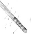
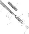
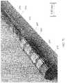
- FIG. 1One embodiment of a microelectrode device illustrated in FIG. 1 includes an elongated microelectrode probe assembly 100 sometimes referred to as an electrode lead.
- the microelectrode probe assembly 100includes an elongated cylindrical member, or body 102 including a microelectrode array 104 located relative to a distal end and one or more electrical contacts located relative to a proximal end.
- the exemplary microelectrode probe assembly 100includes a microelectrode array 104 adjacent to its distal tip.
- the microelectrode array 104has four electrically conductive, cylindrical microelectrode elements 103 disposed along an exterior surface of a cylindrical substrate. The microelectrode elements 103 are microfabricated and wrapped around the cylindrical member 102.
- the microelectrode probe assembly 100also includes four electrically conductive, cylindrical contacts, or contact rings 106a, 106b, 106c, 106d (generally 106) distributed along a longitudinal axis of the proximal end of the assembly 100.
- each of the microelectrode elements 103is in electrical communication with a respective one of the proximal contacts 106 via a respective electrical conductor 108.
- all of the electrical conductors 108are disposed within an interior region of the elongated cylindrical member 102. There are no electronics on this device 100. In use, signals are directed from an implantable pulse generator to the microarray. The length of the cylinder can vary.
- the microelectrode probe assembly 100is preferably sized and shaped for its intended neurological application.
- the microelectrode probe assembly 100may be at least partially placed within the central nervous system.
- the microelectrode probe assembly 100may be at least partially placed within other parts of the body, such as the retina, the cochlea, the epidural space of the spine, and other locations within the peripheral nervous system.
- the diameter and length of the microelectrode probe assembly 100may vary depending on the particular anatomical target.
- the configuration of the microelectrode array 104is also sized and shaped for an intended neurological target. The number, shape, orientation, size, and spacing of the microelectrode elements 103 of the array 104 can be defined in response to the intended neurological target.
- one or more of the microelectrode elements 103are sized and or spaced to record from and/or stimulate a single neuron.
- the microelectrode probe assembly 100can be used to detect and/or record neuronal activity at the neurological target. Neuronal activity naturally occurring within the neurological target gives rise to local electromagnetic fields that can be detected by one or more of the microelectrode elements 103 of the microelectrode array 104. For example, electric fields produced by neurons will polarize one or more of the microelectrode elements 103. Such polarization gives rise to an electrical potential with respect to a reference, such as electrical ground, or another one of the microelectrode elements 103.
- Such electric activitycan be further conducted to one or more of the cylindrical contacts 106 through the internal electrical conductors 108.
- One or more of the cylindrical contacts 106can be connected to one or more additional medical devices for further processing of the detected electrical activity.
- the cylindrical contacts 106can be coupled to a display device or recording device for displaying and/or recording electrical activity from the neurological target.
- one or more of the microelectrode elements 103can be used to electrically stimulate the neurological target.
- one or more externally generated electrical signalscan be applied to one or more of the cylindrical contacts 106. These electrical signals can be conducted through the internal electrical conductors 108 to one or more of the microelectrode elements 103 of the microelectrode array 104.
- an electrical fieldwill be induced by the polarized microelectrode elements 103. Electrical fields induced by such polarization can interact with one or more neurons at the neurological target.
- a microfabrication procedurecan be used to implement electrically conductive traces within an insulative substrate to form any of the microelectrode array devices described herein, whether the array devices are rigid or flexible.
- the microfabricated componentsinclude portions of the microelectrode array assembly.
- the microelectrode arraycan be implemented in a polymeric material such as polyimide or parylene and includes thin film or plated layers of a metal or metal oxide with high charge transfer capability such as platinum, platinum-iridium, iridium, iridium oxide or titanium.
- other metals, metal alloys, and electrically conductive materialssuch as doped semiconductors, conductive polymers, and conductive ceramics may be used.
- the polymeric and metallic layersare deposited sequentially and formed using established principles of microfabrication such as spin coating, DC/RF sputtering, photolithography, plasma etching, and etching with a mask consisting of a secondary or sacrificial material such as silicon dioxide or photosensitive resist.
- the metallic layeris formed to create one or more of the microelectrode array elements and electrically conductive traces that connect the array elements to one or more of the electronics, when included, internal electrical conductors of the elongated cylindrical member, and housing.
- the microelectrode arrayincludes multiple layers.
- the polymeric layersserve to isolate the traces from each other, while also providing the structure of the implant's stimulating/recording tip. There are several fabrication methods which can be described to build such a microfabricated component.
- the insulative substratecan be a polymer, such as a polyimide or parylene but can also be polyurethane or polysiloxane (silicone), or any other suitable insulator.
- a rigid or semi-rigid substratecan be included.
- the microelectrode array deviceis formed on at least one surface of a rigid substrate, such as a planar ceramic member.
- one or more rigid or semi-rigid supporting memberscan be attached during fabrication to provide a desired amount of rigidity.
- the microfabricated componentcan be fabricated, for example, using a series of additive and subtractive processes that produce a stack of materials.
- Mechanical components of the implantable neurological probe assembly 100include the elongated cylindrical member 102, which can be a simple polymeric cylinder.
- the cylindrical membermay be composed of two concentric tubes with wire traces wrapped around the inner tube, in the space between the concentric tubes.
- the elongated cylindrical member 102can vary in length and diameter but is generally at least about 28 cm long, and around 1.27 mm in diameter.
- the microfabricated componentis wrapped around an external surface of the cylindrical member 102.
- the microfabricated componentis wrapped around an additional tube at the distal end of the cylindrical member 102.
- the microfabricated componentscan be attached to the cylindrical member 102 to protrude at the distal tip, from the cylindrical member's interior.
- the cylindrical member 102also contains electrical wires 108 within that connect at one end to the microfabricated component, at another end to the cylindrical contacts 106 for interconnection to an implantable pulse generator.
- one or more of the microfabricated components and the elongated cylindrical member 102include one or more electrical components.
- the electrical componentscan be discrete or microelectronic parts. Their purpose is to filter, route, generate, or process signals to and from the microelectrodes. They can be attached to the microfabricated part during production, or bonded afterwards. They will generally be contained within the mechanical component.
- the neurological probe 100can be implanted near a neurological target, such as a target brain structure, using common neurosurgical techniques such as stereotaxy or endoscopy.
- the neurological probe 100can be inserted without support, or within a supporting cannula having an inner dimension slightly larger than the outer dimension of the device.
- the cannulawhen used, would be retracted once the neurological probe 100 has been suitably positioned.
- a lumen along the axis of the cylindrical member 102permits the insertion of a rigid stylet which renders the neurological probe 100 rigid during surgical implantation. This is particularly helpful during insertion, positioning and repositioning of flexible embodiments of the neurological probe 100.
- the styletis removed after implantation leaving the probe in its surgical target.
- a cliniciancan connect one or more of the microelectrode elements to a display unit or a recording unit through the cylindrical contacts 126.
- the recording unitnot shown, allows a clinician to identify certain regions of the brain according to their electrical activity. In some embodiments, such recording information can be processed automatically, through the use of a suitably programmed computer processor.
- the electrodes used to record from the braincan be the same electrodes as those used to stimulate tissue.
- the recording electrodescan also be separate from those used to stimulate the brain. This situation might be preferred because electrodes destined for recording may be different in size and design than those for stimulation.
- the operatorcan connect the electrodes to an external stimulation source or an implantable source.
- the sourcecan include a pulse generator for applying signals to the electrode sites.
- the signals from such a pulse generatorcan be connected directly to the electrodes, or they can be preprocessed using electronics embedded in the device.
- the electronicscan filter certain parts of the original signal. If there are more electrodes than signals, the electronics can route or otherwise interconnect the stimulation source as necessary.
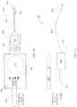
- FIG. 2A perspective view of the portion of a human anatomy is illustrated in FIG. 2 , showing implantation of an exemplary elongated microelectrode probe assembly 124 position for interaction with a neurological target located deep within the brain.
- a distal portion of the microelectrode probe assembly 124is positioned at the neurological target 130, in this instance located within the human brain 132.
- the proximal end of the microelectrode probe assembly 124is connected to a first medical device 128.
- the first medical device 128may include an electronic assembly implanted external to the brain 132 to minimize invasion into the brain and flesh or to facilitate wireless access to the electronic assembly 128.
- a second medical devicewhich again may include an electronic assembly such as a pulse generator 122 can be implanted at a remote portion of the subject body. As shown, a second electronic assembly 122 is implanted within a chest cavity 120.
- a cable 126may also be implanted within the subject's body to interconnect the pulse generator 122 to the electronic assembly 128, when present or directly to cylindrical contacts located at the proximal end of the microelectrode probe assembly 124.
- FIG. 3a cross-sectional view of a portion of an anatomy 148 is shown, illustrating an exemplary microelectrode probe assembly 140 positioned at a neurological target 150 (e.g., subthalamic nucleus, shown).
- the microelectrode probe assembly 140includes an array of microelectrode elements 142a, 142b, 142c, 142d (generally 142) distributed along an elongated, cylindrical supporting structure 144.
- the microelectrode probe assembly 140is shaped and sized to allow one or more of the microelectrode elements 142 to be positioned at the neurological target 150.
- materials used in construction of microelectrode probe assembly, as well as one or more of its construction features, size, shape, and orientationcan be selected for biocompatibility.
- each microelectrode element 142c of the microelectrode probe assembly 140are positioned in intimate contact with the neurological target 150.
- each microelectrode elementis configured here as an annular array of sub-elements 145, 151.
- the sub-elements 145, 151can be distributed about a circumference of the probe assembly 140, at a common axial displacement from the distal end. It is understood that some sub-elements of such an annular array 142c can be in contact with the neurological target, while other sub-elements of the same annular array 142c are not (as shown).
- One or more additional microelectrode elements 142 of the probe assembly 140may reside at locations not in the immediate vicinity of the neurological target 150.
- one or more of the microelectrode elements 142are remotely accessible from a proximal end of the probe assembly 140 via one or more electrically conductive leads (not shown).
- selectable sub-elements 145, 151can be activated to record and or stimulate the target 150.
- recordings of neurological activity from sub-elements 145 in contact with the target 150can be used to identify the location of the target 150 relative to the probe assembly 140.
- only those sub-elements 151 in contact with the targetmay be activated to stimulate the target.
- thismay result in an annular array 142 stimulating a selectable angular region about the probe assembly 140.
- any of the supporting structures described herein, such as the supporting structure 144 illustrated herecan be a ridged, or semi ridged structure, such as a polymeric cylinder.
- the structurecan be a flexible structure, such as one or more flexible substantially non conducting substrate (i.e., a bi-electric ribbon) onto which the microelectrode elements 142 are formed as electrically conductive film layers.
- the one or more microelectrode elements 142are in communication with electronic circuitry (not shown) through one or more electrical leads (not shown) that can be routed through an internal lumen of a supporting structure 144 and/or formed using elongated film layers along a flexible, ribbon like supporting structure 144.
- the microelectrode elements 142can be placed into the brain generally for recording and/or stimulation of the cortex and for deep brain stimulation and/or recording of neurological targets including the subthalamic nucleus and the globus pallidus.
- the microelectrode elements 142can also be placed in other parts of the body, such as the retina, the spine, the peripheral nervous system for neural recording and/or neural stimulation of such portions of an animal anatomy.
- microelectrodesare discussed generally throughout the various embodiments, there is no intention to limit the upper or lower size of the microelectrodes.
- the devices and methods described hereinare generally scalable, with a microelectrode size determined according to the intended application.
- microelectrodesare dimensioned sub-millimeter. In some embodiments, microelectrodes are dimensioned sub-micron. In some embodiments, the microelectrodes are formed as planar structures having a diameter of about 50 ⁇ m that are arranged in a linear array with center to center spacing of about 100 ⁇ m.
- the planar structure of the microelectrodescan have regular shapes, such as circles, ellipses, polygons, irregular shapes, or a combination of such regular and/or irregular shapes.
- This probe assembly 140is implantable near a neurological target, such as a target brain structure, using common neurosurgical techniques such as stereotaxy or endoscopy.
- the devicemight be inserted without support or within a cannula which may have an inner dimension slightly larger than the outer dimension of the device.
- the devicemay have a rigid stylet running along its central axis with an outer diameter that is smaller than the inner diameter of an axial lumen in the device. When used, such a cannula, or a stylet, is generally retracted once the device is in position.
- the operatorcan connect the probe assembly 140 to a recorder unit configured to identify certain regions of the neurological target (e.g., the brain) according to the electrical activity detected by the probe assembly 140.
- the microelectrode elements 142 used to record from the neurological target 150can be the same microelectrodes as those used to stimulate the target in applications in which both recording and stimulation are accomplished.
- the microelectrode elements 142 used to record from the neurological target 150can be separate microelectrode elements 142 from those used to stimulate the target 150. This is demonstrated in this embodiment, in which each microelectrode assembly includes one or more recording electrodes 145 and one or more stimulating electrodes 151. As shown, the dedicated recording electrode 145 is smaller than dedicated stimulation electrode 151.
- microelectrodes destined for recordingmay differ in one or more of size, shape, number, and arrangement from those microelectrodes destined for stimulation, e.g., using different microelectrodes.
- the microelectrode elements 142 configured for stimulationcan be connected to a stimulation source through one or more interconnecting leads.
- the stimulation sourcecan be in vivo.
- Any implanted elements of the stimulation sourceare preferably fabricated and/or contained with a hermetically sealed, bio-compatible envelope.
- bio-compatible packaging of signal sourcesis well known, for example, in the area of artificial pacemakers.
- the stimulation sourcewhen provided, may be a controllable signal generator producing a desired signal according to a prescribed input.
- the signal generatormay receive an input indicative of a desired output stimulation signal frequency.
- Such output stimulation signalscan have a variety of wave forms, such as pulses, charged balanced pulses, sinusoidal, square wave, triangle wave, and combinations of such basic wave forms.
- the stimulation sourceincludes a pulse generator for applying signals to the microelectrodes site.
- the signals from the pulse generatorcan be connected directly to the microelectrodes, or they can be preprocessed using electronics.
- preprocessing electronicsare embedded within the implantable device.
- the preprocessing electronicscan filter certain parts of an original signal, such as a cardiac pacemaker signal, in order to select preferred frequency components of the original signal that are at or near a peak resistance frequency of the microelectrodes.
- electronicscan route the stimulation signals to preferred one or more of the microelectrodes.
- the microelectrode array 104includes a formable planar substrate 160.
- One or more electronically conducting regions 162are disposed along portions of the formable planar substrate 160.
- the microelectrode probe assembly 100can be formed using a polyimide structure (e.g., 160) containing multiple microelectrode elements wrapped and molded in place around an elongated, cylindrical polyurethane body.
- the electronically conducting regions 162, or microelectrode elementsare thin-film conducting bands extending around a substantial circumference of an external surface of the elongated cylindrical member 102.
- the four conducting bands 162can be electrically coupled to an implantable pulse generator. In some embodiments, one or more of the conducting bands are coupled to the implantable pulse generator through an impedance match circuit (not shown).
- the electrically conductive electrode width in this exampleis about 700
- the electrically conductive microelectrode elements 162can be formed using metals, suitably doped semiconductors, conductive polymers, conductive ceramics, and combinations thereof.
- the formable planar substrate 160includes a longitudinal extension 164.
- This longitudinal extension 164may include one or more electrical circuit elements such as one or more electrically conductive wire-lead contacts 168 as shown.
- One or more of the electrically conductive circuit elements, such as the wire-lead contacts 168may be in electrical communication with one or more of the electrically conducting bands 162 through interconnecting traces 166 extending between the wire-lead contacts 168 and the electrically conducting bands 162.
- the microelectrode array 104is located along an external surface of the elongated microelectrode probe assembly 100.
- Other portionssuch as the longitudinal extension 164 maybe located within an interior portion of the elongated cylindrical member 102.
- each of the internal electrical conductors 108is illustrated extending along an interior portion of the elongated cylindrical member 102. Distal tips of each of the internal electrical conductors 108 are in electrical communication with a respective one of the wire-lead contact 168 as illustrated.
- the microelectrode array 180can be prepared as a micro-electromechanical system (MEMS).
- MEMS film device 180can be prepared from a substantially electrically insulative planar substrate 182 onto which the electrically conductive elements are formed.
- a dielectric planar substrate 182is prepared to include electrically conductive surfaces corresponding to the multiple elements of the microelectrode array.
- a four element microelectrode array of electrically conducting elements 184a, 184b, 184c, 184d(generally 184) is formed on a polyimide substrate.
- the formable planar substrate 182includes a longitudinal extension 186.
- One or more of the microelectrode array elements 184can be connected to one or more other circuit elements such as lead wire traces 186 provided on the longitudinal extension 185.
- Such a devicecan be prepared using standard MEMS techniques by which the substrate and conductive elements are prepared in a planar configuration and later formed into a non-planar shape.
- the four-element microelectrode array 184can be formed into a substantially cylindrical shape to accommodate an outer surface of an elongated cylindrical member of a microelectrode probe assembly.
- the MEMS device 180is shown attached at a distal tip of an elongated cylindrical member 192.
- the electrically conductive surface of the four-element microelectrode array 184remains exposed about the outer surface of the elongated cylindrical member 192.
- the microelectrode array 184is positioned for intimate contact and interaction with any neurological target into which the elongated cylindrical member may be placed.
- FIG. 7AAn alternative embodiment of a neurological probe 200 is shown in FIG. 7A .
- This neurological probe 200also includes a formable film substrate 205 shown placed at a distal end of an elongated cylindrical body 202.
- the cylindrical body 202is formed by two coaxial cylindrical members.
- At a proximal endare eight cylindrical contacts 206, which electrically connect the proximal end to the film substrate 205 at the distal end through lead wires within the coaxial cylindrical members 202.
- FIG. 7Ba more detailed view of the distal end is shown.
- Formed along an outer surface of the formed cylindrical substrate 205are multiple circumferential segmented microelectrode elements 204 and 207 spaced apart along both longitudinal and circumferential axes.
- eight such conductive microelectrode elementsare included.
- Microelectrode elements 204are segmented such that three microelectrodes at a common axial location are disposed about a circumference of the neurological probe 200, referred to herein as segmented elements.
- Such segmented elements that are independently addressableallow for stimulation a selectable angular region about the probe assembly 140.
- only those sub-elements on one side of the probe 200can be activated to selectively treat a target along the same side of the probe. More than one sub-element can be activated to selectively treat a desired angular region disposed about the probe, including a region tending 360 deg. or less. In this regard, the probe can be said to focus energy toward a desired region.
- Microelectrode elements 207are not segmented, therefore one electrode covers the entire circumference of the neurological probe 200.
- the assemblycan include an end cap 209, which covers the end of the cylindrical tubing.
- the assemblycan also include a support tube 215 onto which the microelectrode film can be attached, e.g., by gluing or heating.
- each contact of the eight cylindrical contacts 206is electrically coupled to a respective one of the microelectrodes 204, 207.
- FIG. 7Cdemonstrates the shaping required for the microelectrode film 205 in order to be assembled.
- the microelectrode film 205also includes a longitudinal extension 206.
- the extension 206incorporates contact pads 211, each pad 211 in electrical communication with a respective one of the microelectrode element 204, 207, for example, through electrical traces.
- Both the distal and proximal ends of the microelectrode film 205are reshaped, for example using heating, into a cylindrical shape as shown. Other shapes are possible, depending on the cross-sectional profile of the support tube 218 (e.g., triangular, oval, rectangular).
- FIG. 7Dillustrates the assembly of the neurological probe 200 in more detail.
- the assemblyconstitutes two overlapping, concentric cylindrical members 213 and 214.
- Inner cylindrical member 213defines a lumen with a typical diameter of 400 ⁇ m.
- the outer diametercan be 1 mm, but must be less than the inner diameter of outer cylindrical member 214.
- Both cylindrical members 213 and 214can be composed of a polymeric, rigid or non-rigid (e.g., semi-rigid or flexible) material such as polyurethane or silicone.
- the assemblyalso constitutes eight lead wires 212 extending longitudinally in a space defined between the cylinders 213, 216. In some embodiments, the lead wires 212 are helically wrapped around inner cylindrical member 213.
- Lead wires 212generally have a diameter of 50-125 ⁇ m.
- the assemblymay optionally include a rigid or semi-rigid support tube 215 at its distal end.
- the tube 215is used as a support structure onto which the microelectrode film 205 can be attached.
- the microelectrode film 205is attached via its contact pads 211 to electrical lead wires 212, each lead wire 212 contacting a respective one of the contact pads 211.
- the tube 215can cover these connections adding strength to their structure.
- the microelectrode film 205is then wrapped in the direction of the arrow.
- end cap 209covers and seals the cylindrical members 213 and 214.
- the end capcan be shaped, for example, having a blunt profile, as shown.
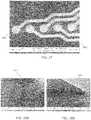
- FIG. 7Edemonstrates an image of an assembled neurological probe 200.
- the different components described in FIG. 7A through FIG. 7Dare visible including the microelectrode array film 205, the inner tubing 213 and the outer tubing 214.
- the distal support tube 215has been implemented as a laser cut stainless steel tube.
- FIG. 8A and FIG. 8BAnother embodiment of an elongated microelectrode probe assembly 220 is illustrated in FIG. 8A and FIG. 8B , including a microelectrode array assembly 224.
- the microelectrode array assembly 224is positioned at a distal end of an elongated cylindrical member 222.
- one or more electrically conductive, cylindrical contactsare positioned at a proximal end of the elongated cylindrical member. As shown, there are four such cylindrical contacts 226. In other embodiments, there may be more or fewer contacts.
- the microelectrode array assembly 224also includes a microelectronics assembly 233 positioned along an offset longitudinal extension 232 of the assembly.
- the longitudinal extension 232is offset such that the microelectronics assembly 233 is contained within an interior region of the elongated cylindrical member 222, thereby protecting the microelectronics assembly 233 from interaction with the surrounding biological environment.
- One or more internal electrical conductors 228extend from the longitudinal extension 232 to one or more of the cylindrical contacts 226.
- the longitudinal extension 232is also in electrical communication with the conductive electrodes of the microelectrode array 230 through one or more lead traces 234. Also shown are the connections between the internal electrical conductors 228 and a proximal end of the longitudinal extension 232.
- electrical activity from a neurological targetcan be detected by one or more of the microelectrode contacts 231 of the microelectrode array 230.
- the electrical signalsare then routed through the lead traces 234 to the microelectronics assembly 233.
- the microelectronics assembly 233may process the detected electrical signals, for example, through pre-amplification and routing.
- the processed electrical signals detected from the neurological targetare routed through the internal electrical conductors 228 to the cylindrical contacts 226.
- One or more external medical devicessuch as a recorder may be connected to the elongated microelectrode assembly 220 through the cylindrical contacts 226 for display and or recording of the detected electrical activity.
- One or more of the cylindrical contacts 226can be used to communicate with the microelectronics assembly 233 through one or more of the internal electric conductors 228 in order to remotely or externally control operation of the microelectronics assembly 233.
- an external signalmay be used to select which one or more of the microelectrode contacts of the microelectrode array 230 are selected for recording.
- recordingcan be accomplished for all of the microelectrode contacts of the microelectrode array 230.
- the microelectronics assembly 233may include a multiplexer for combining the signals from more than one of the microelectrode elements 231 onto one of the cylindrical contacts 226.
- a multiplexerfor combining the signals from more than one of the microelectrode elements 231 onto one of the cylindrical contacts 226.
- multiplexing techniquescan be used to combine one or more of the cylindrical contacts 226 to one of the microelectrode elements 231.
- two contacts 231can be coupled to one of the distal contacts 226, such that four contacts 226 are sufficient for accessing all eight microelectrode elements simultaneously.
- Such multiplexingmay include any suitable form, such as time division multiplexing, frequency division multiplexing, code division multiplexing, and combinations of one or more of these techniques.
- the microelectronics assembly 233perform at least some level of processing of the detected neurological activity.
- the microelectronics assembly 233may be a purely routing device connecting one or more selected microelectrode elements 231 to one or more of the cylindrical contacts 226.
- Such a microelectronics assembly 233may be a simple switch or router device.
- Such routingmay include electromechanical switches, reed switches, and electronic switches, such as transistor (e.g., field effect transistor) switches.
- the switchescan be configured in a matrix fashion to allow one or more of the microelectrode elements 231 to be in communication with one or more of the microelectronics assembly 233 and the internal electrical conductors 228 based on a control input signal as may be received from an external source through one or more of the contacts.
- the microelectronic devicemay include signal conditioning circuitry such as one or more of amplification, filtering, and attenuation.
- signal conditioningmay include one or more of electronic filtering to tailor a frequency spectrum of the detected signal and attenuation.
- Such electronic filteringcan be accomplished with any suitable filter known to those familiar with electronic signal processing.
- filtersmay include low pass, high pass, band pass and combinations of one or more of these.
- the filtersmay be implemented with standard circuit elements, such as inductors, capacitors, and resistors. Alternatively or in addition, at least some of the filters may be implemented using digital signal processing techniques.
- the microelectronics assembly 233may include one or more of an Application-Specific Integrated Circuit (ASIC), commonly available electronics modules, such as microprocessors, electronic memory elements, communications devices, combinational logic, power conditioning, and the like.
- ASICApplication-Specific Integrated Circuit
- the longitudinal extension 232includes a planar film substrate 242.
- the substrate 242includes a first group of one or more electrical contacts in the form of bonding pads 244, sized and positioned to accommodate one or more devices of the electronics assembly 230 ( FIGs. 8A , 8B ).
- the substrate 242also includes a second group of one or more additional electrical contacts in the form of wire bonding pads 246, sized and positioned to accommodate interconnection to one or more of the interconnecting lead wires 228.
- At least some of the bonding pads 244 of the first groupare coupled to respective lead wire traces 248 interconnecting the bond pads 244 to respective ones of the microelectrode contacts 231.
- the longitudinal extension 232includes the microelectronics assembly 233 housed thereon and the interconnecting lead wires 228 coupled to the second group of bonding pads 246.
- FIG. 11A and FIG. 11BAnother embodiment of an elongated microelectrode probe assembly 420 is illustrated in FIG. 11A and FIG. 11B .
- the assembly 420includes a microelectrode array assembly 260 at a distal tip of the probe assembly 420 as shown.
- This microelectrode array assembly 260can be any microelectrode array including any of the microelectrode arrays described herein.
- the assembly 420also includes one or more cylindrical contacts 426a, 426b, 426c, 426d (generally 426) at a proximal end, as shown.
- the microelectrode array assembly 260 and cylindrical contacts 426are disposed along a flexible elongated cylindrical member 422.
- the cylindrical member 422includes an elongated open-ended lumen 424, accessible from an open end 430 located at a proximal end of the probe assembly 420.
- One or more internal electrical conductors 428extend from the microelectrode array assembly 260 to the one or more cylindrical contacts 426.
- the internal electrical conductorsare configured so as not to interfere with interior volume of the open ended lumen 424 or with flexibility of the elongated cylindrical member 422.
- four such electrical conductors 428are shown extending helically along the length of the elongated cylindrical member, between the microelectrode array assembly 260 and the cylindrical contacts 426.
- These helically wound internal electrical conductors 428reside within the material of the flexible elongated cylinder 422 between an exterior surface and an interior wall of the open ended lumen 424.
- an elongated rigid guide membersuch as a stylet, or trocar (not shown) can be inserted into an open end 430 of the open ended lumen 424 extending along a substantial length of the elongated flexible cylindrical member 422 to provide temporary rigidity as may be necessary during insertion and/or removal procedures of the elongated electrical probe assembly 420.
- a styletprovides rigidity as the elongated electrical probe assembly 420 is inserted into a neurological target site. Once inserted at the target site, the stylet can be removed from the proximal open end 430. The remaining elongated electrical probe assembly 420 remains positioned at the target site, while also providing substantial flexibility along its extended length.
- the styletmay be configured as a straight element.
- at least a portion of the styletmay include a non-linear region, such as a curve, as may be beneficial to facilitate insertion and/or removal of the elongated electrical probe assembly 420.
- the microelectrode array assembly 260extends for a length 'T' along longitudinal axis.
- the elongated flexible cylindrical member 422has a diameter 'D'.
- Four cylindrical contacts 426 at the proximal endcan provide access to power 426a, electrical ground 426b, control 426c, and signal or data 426d.
- FIG. 11BA more detailed view of a distal portion of the elongated electrical probe assembly 420 shown in FIG. 11B illustrates distal ends of each of the helically wound internal electrical conductors 428, connected to respective lead wire bonding pads 436 as may be provided on a longitudinal extension 434 of the microelectrode array assembly 260. Also visible is the distal portion of the open ended lumen 424, having a distal end 432 located relatively close to a proximal end of the longitudinal extension 434. Thus, the open ended lumen 434 extends along nearly the entire length of the elongated flexible cylindrical member 422. When the stylet is inserted within the open ended lumen 424 and extends toward the distal end 432, the elongated flexible cylindrical member 422 has temporary rigidity along substantially its entire length.
- the deviceincludes a microelectrode array 260, located adjacent to the distal tip 438.
- the microelectrode array assembly 260includes a longitudinal extension 434 housing one or more microelectronic devices 440 and including electrical contacts, each in respective communication with one of the internally electrical conductors 428.
- the assembly 260includes a hollow cylindrical substrate 262.
- the exemplary embodimentincludes sixteen semi-annular microelectrodes 268 arranged in annular sub-arrays positioned at respective distances along a longitudinal axis of the cylindrical substrate 262 for example being measured from a distal end.
- each annular sub-arrayincludes four stimulation electrodes 268 and four recording electrodes 269.
- Other numbers of sub-array elementsare possible, and it is not necessary that the number of stimulation electrodes 268 be equivalent to the number of recording electrodes 269 for any given sub-array.
- each sub-arrayis identical, while in other embodiments, they differ.
- each stimulation electrode element 268extends along an arc length greater than 10° but less than 180°.
- Each recording electrode 269extends along an arc length substantially less than 90° such that the combination of stimulation electrode elements 268 and recording electrode elements 269 are disposed about 360° of the cylindrical substrate 262 with suitable spacing provided between each of the adjacent elements 268, 269.
- the stimulation electrode elements 268appear as stripes located about their respective distances along the central axis; whereas, the recording electrodes appear as small circles, or dots.
- the particular shape of the recording electrode elements 269can be circular, elliptical, polygonal, such as squares, triangles, diamonds, hexagons, and the like.
- the shape of the stripe ends of the stimulation electrode elements 268 adjacent to the recording electrode 269may be angular (e.g., square) or curved. As shown in the figure, a reference angle is measured with respect to a seam at 0° extending around the circumference.
- the recording electrodes 269are located adjacent to the seam 264 at approximately 0°.
- a second recording electrode located opposite to the firstresides at approximately 90°.
- the stimulation electrode element 268is centered at approximately 45°, between approximately 15° and 75°.
- a second stimulation electrode 268is located centered at 135° and also extending between approximately 105° and 165°.
- a third recording electrode 269is located at approximately 180°.
- a third stimulation electrode 268is located centered at 225°, extending between approximately 195° and 255°.
- a fourth recording electrode 269is located at approximately 270°.
- a fourth stimulation electrode 268is located centered at 315° extending between approximately 285° and 345°.
- a longitudinal extension to the substrate 272including in this example thirty two electronic device contacts 274, each one in electrical communication with a respective one of the dedicated recording or dedicated stimulating electrodes via interconnecting lead traces. Also disposed on the longitudinal extension 272 are one or more wire lead contacts 276. In the illustrative example, four such wire lead contacts 276 are provided.
- FIG. 12Illustrated in FIG. 12 is an electronic circuit schematic diagram for half of the microelectrode array assembly 260 shown in FIG. 11D . Shown along the right hand portion of the schematic diagram are the eight of the sixteen stimulation electrode elements 268a through 268h (generally 268). Each one of these elements 268 is in electrical communication with a respective electronic device contact 274a through 274d and 274m through 274p (generally 274). Also illustrated along the right hand portion of the schematic diagram are eight of the sixteen recording electrode elements 269a through 269h (generally 269). Similarly, each of the recording electrode elements 270 is in electrical communication with a respective electronic device contact 274e through 274h and 274j through 2741.
- the schematic diagramincludes a representative electronic device 280.
- the schematic diagramincludes only eight recording and eight stimulation contacts but a full schematic diagram for all thirty-two contacts is similar.
- this electronic devicemay include one or more of a switch or router, a preamplifier, a signal conditioner, a multiplexer, and a controller.
- the electronic device 280is in electrical communication with all sixteen of the electronic device contact elements 274a through 274p.
- the electronic device 280is in further communication with each of the four wire lead contacts 276a through 276d (generally 276).
- the first wire lead contact 276ais used for supplying electrical power to the microelectronic device and/or one or more of the stimulation electrode elements 268.
- the second wire lead contact 276bis used to provide an electrical ground contact.
- This ground contact 276bmay include earth ground, another electrical ground within the system, such as a chassis ground of a medical device connected to the electronic device 280, or simply a signal return line.
- a third wire lead contact 276ccorresponds to a control signal that may be used to provide control inputs from an operator or other medical device, to control configuration and/or operation of the electronic device 280.
- control signal contact 276cmay be used for control signals from the electronic device 280 to another medical device.
- a fourth wire lead contact 276dcorresponds to a signal contact as may be used for directing electrical activity detected by one or more of the recording electrode elements 269 to a recording or display device.
- the signal contact 276dmay be used for directing electrical stimulation signals from another medical device to one or more of the stimulation electrode elements 268.
- the stimulation electrodes 268are configured to have a relatively low electrical impedance; whereas, the recording electrodes 269 are configured to have a relatively high electrical impedance.
- a relatively low impedance stimulation electrodes 268are therefore well suited for transfer of electrical charge transfer to surrounding tissue at a neurological target site.
- the relative high impedance recording electrodes 269allow for detection of electrical activity from a neurological target site.
- FIG. 13Adisplays an additional embodiment of a neurological probe 200, incorporating embedded microelectronics.
- the neurological probe 200incorporates a microelectrode film 202, and cylindrical member 203 composed of two concentric cylindrical tubes, and eight electrical contacts 201 that permit electrical connection from the distal end to the proximal end through eight lead wires wrapped around the inner cylindrical member.
- FIG. 13Bprovides a more detailed view of an embodiment of the distal end of the neurological probe 200.
- the metallic stimulation electrode 248has dimensions in this example of about 1000 ⁇ m in length, and 600 ⁇ m in width. In some embodiments, the length measured along the longitudinal axis can range from 2 ⁇ m to 2 mm. In some embodiments, the width may cover the entire circumference, and can range from 2 ⁇ m to 4 mm.
- the metallic recording electrode 249has dimensions in this example of 150 ⁇ m in diameter. It is generally smaller than the stimulation electrode 248.
- the distal endincorporates a support tube 229, that serves as a support structure for the microelectrode film 202 and as a protective enclosure for the microelectronic circuit and connections within.
- the tube 229has a length of 8 mm, an inner diameter of 1.05 mm, and an outer diameter of 1.25 mm. It may be implemented in a rigid, or semi-rigid material such as stainless steel, or a biocompatible polymer such as PEEK (polyetheretherketone).
- the embodimentalso demonstrates the outer cylindrical member 203 which is implemented with an outer diameter of 1.27 mm, and an inner diameter of 1.05 mm. It is generally implemented in polyurethane or silicone. Along its lumen are wrapped the lead wires 221 that electrically connect the proximal and distal ends of the neurological probes.
- the outer cylindrical member 203can be connected to the support tube 229 by form fitting or gluing.
- the embodimentalso demonstrates an end-cap 241 which can be implemented as a plug to seal the ends of the two concentric tube structures.
- the microelectrode film 202is connected to the inner volume by an extension 208 that leads to the embedded microelectronic element and lead wires 221.
- FIG. 13Ca cutaway view of the distal end of the neurological probe 200 is provided in order to identify the microelectronic element at its interior.
- the longitudinal extensionis offset from an external surface of the cylindrically formed substrate 202 such that the longitudinal extension 206 and any microelectronic devices 210 mounted thereon would be containable within an interior region of the elongated cylindrical member housing the formable film substrate 202.
- the formable film substrate 202 including the conductive electrodesis wrapped around a cylindrical body 229 located at the distal end of the neurological probe.
- a selection circuitsuch as a switch or router, can be included to selectably route stimulation or recording signals to/from one or more of the microelectrode rings thereby stimulating or recording from a selectable location within the neurological target depending upon which microelectrode ring(s) is in use.
- stimulation signalsmay be routed from the implantable pulse generator 122 ( FIG. 2 ) and applied to a chosen microelectrode ring.
- the microelectrode filmcan be initially formed as a flat element onto which a microelectronic circuit element is mounted before, or after, it is assembled into two concentric cylinders.
- the longitudinal extension 206can be configured to accommodate one or more microelectronic devices 210.
- One or more of any such microelectronic devices 210 included thereoncan be in electrical communication with one or more of the microelectrode elements 248 and 249 through one or more interconnecting conductive electrical traces 208.
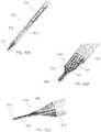
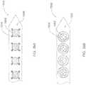
- FIG. 14Aa microelectrode array 300 is illustrated placing many relatively small microelectrodes 302 around a central cylinder.
- eight such elements 302are located at respective positions around 360° circumference of the cylinder, forming an annular microelectrode pattern 303.
- the angular displacement between adjacent elementsmay be uniform as shown (e.g., eight elements spaced apart from each other by 45°).
- the angular displacement between at least some of the adjacent elements 302 of the annular microelectrode pattern 303may be non-uniform.
- Additional annular patterns of elementscan be positioned along the cylinder. For example, the same pattern can be repeated at different distances along the cylinder as measured with respect to an end of the array 300.
- the distance between adjacent annular patterns 303may be uniform.
- the distance between adjacent annular patterns 303 of the microelectrode array 300may be non-uniform.
- there the array 300includes four identical annular patterns 303 uniformly spaced apart along the central cylinder.
- the annular microelectrode pattern 303includes eight microelectrode 302 discs, each having a diameter of about 300 ⁇ m, uniformly distributed and wrapped around a 1.27 mm diameter cylinder.
- the microelectrodes 302could be other shapes, such as ellipses, polygons, such as squares, triangles, diamonds, hexagons, and the like.
- One or more of the shapes and sizes of the microelectrodes 302may vary within the annular microelectrode pattern 303. For example, sizes may range from 2 ⁇ m or less, to 1 mm or larger.
- the electronics required to apply electrical signals to the microelectrode sites, or to record neural activity from the sites,are embedded within the central cylinder.
- FIG. 14BAn alternative embodiment of the invention illustrated in FIG. 14B shows several microelectrode elements 312 configured lengthwise, extending along a longitudinal axis of the cylinder and disposed at respective angles measured about a circumference of the cylinder.
- each microelectrode element 312is a strip having a diameter of about 300 ⁇ m and length of approximately 1.88 mm, extending along the length of the cylinder.
- Eight such elongated strip microelectrode elements 312are uniformly distributed and wrapped around a 1.27 mm diameter cylinder.
- the ends of the microelectrodesmay be angular (e.g., square) or rounded as shown.
- the dimensions of the elongated strip microelectrode elements 312may range in width from 2 ⁇ m or less, to 1 mm or larger. They may range in length from 2 ⁇ m or less, to 3 mm or longer.
- FIG. 15A through FIG. 15Jrepresent various embodiments of microelectrode arrays.
- Each of the microelectrode arraysis illustrated in a planar representation.
- these planar representationswould be folded about the cylindrical structure having a longitudinal axis extending vertically with respect to the planar representation, such that the left and right sides of the planar structure meet along a seam.
- Also illustrated along the top of each figureare reference angular positions varying from 0° to 360°.
- a first microelectrode array 320 illustrated in FIG. 15Aincludes a formable planar substrate 324 including multiple horizontal electrically conductive stripes 322a through 322d (generally 322). When formed in a cylindrical fashion, these horizontal stripes represent cylindrical microelectrode elements 322.
- each of the electrically conductive stripes 322is located at a respective distance 'd 1a ' measured from one of the ends of the formable planar substrate 324 along the longitudinal (vertical) axis.
- Each of the electrically conductive stripes 322has a respective width 'w 1 ' and center to center spacing with respect to neighboring conductive stripe 322 of 's 1 '.
- FIG. 15BAnother embodiment of a microelectrode array 330 is illustrated in FIG. 15B .
- This microelectrode array 330also includes a number of horizontal electrically conducting stripes 332. With respect to the stripes 322 of FIG. 15A , these stripes 332 have a narrower width w 2 , a closer center to center spacing s 2 , and are larger in number. In some embodiments it would be possible to include electrically conducting stripes having one or more of various different widths and different spacing.
- the eight microelectrode strips 332are connected to eight respective bond pads (not shown). In yet additional embodiments, the eight microelectrode strips 332 are connected to four bond pads (not shown), resulting in two adjacent strips being in electrical contact.
- a microelectrode of a given surface areacan be configured to increase its perimeter. This can be accomplished, for example, by controlling shapes of the microelectrodes. Thus, rather than a simple rectangular arrangement, a microelectrode can have a folded shape (e.g., a "U” or and "S" or even a comb-like shape).
- more than one microelectrodeare energized by a common source (e.g., through a common bonding pad).
- two or more of the microelectrode strips 332can be connected to the same respective bond pad. Thus, the eight strips 332 can be controlled through only four bonding pads.
- FIG. 15Cillustrates the microelectrode array 350.
- the microelectrode array 350includes four horizontal annular patterns 356a through 356d (generally 356).
- Each horizontal annular pattern 356includes a first high-impedance element 356a, located at approximately 0° and a second high-impedance element 356b, located at approximately 180°.
- a first low-impedance microelectrode element 358ais located between the two high-impedance microelectrodes 356a, 356b.
- a second low-impedance microelectrode element 358bis located to the right of high-impedance microelectrode element 358b.
- the two high-impedance microelectrodes 356a, 356boppose each other, as do the two low-impedance electrodes 358a, 358b.
- the annular pattern 352is repeated at three other different distances measured with respect to the bottom edge of the formable planar substrate 354. Other embodiments having more or less annular patterns can be included. Such a configuration is useful for increasing microelectrode edges in contract with each bonding pad.
- FIG. 15DAnother embodiment of a microelectrode array 340 is illustrated in FIG. 15D , similar to that shown in the microelectrode array assembly 260 of FIG. 11D .
- This microelectrode array 340is similar to the microelectrode array 350 illustrated in FIG. 15C , except that each of the low-impedance microelectrode elements have been split into two low-impedance microelectrode sub-elements 348a, 348b and 348c, 348d.
- the microelectrode sub-elements 348are electrically isolated from each other, requiring separate bond pads for each element.
- each annular pattern 372includes four high-impedance microelectrode elements 376a through 376d (generally 376) respectively located at approximately 0°, 90°, 180°, and 270°.
- Each of four relatively low-impedance microelectrode elements 378a through 378dis located between adjacent pairs of high-impedance microelectrode elements 376.
- microelectrode recording elements 376are larger and will therefore have different electrical recording characteristics than those demonstrated in FIG. 15D .
- a planar representation of the microelectrode array illustrated in FIG. 14Ais shown in FIG. 15F .
- the microelectrode array 360includes four horizontal annular patterns, each including eight circular microelectrode 366 elements arranged on a formable planar substrate 364.
- FIG. 15Gillustrates a planar version of the microelectrode array 310 shown in FIG. 14B .
- This microelectrode array 390includes eight elongated, vertically conducting microelectrode stripes 392 arranged at uniform spacing between 0° and 360° along the formable planar substrate 394.
- FIG. 15Hillustrates yet another microelectrode array 380 including combinations of the elongated, vertically conducting microelectrode stripes 386 and circular microelectrode elements 384 arranged at respective longitudinal distances along the formable planar substrate 384.
- FIG. 15IAnother microelectrode structure is illustrated in FIG. 15I , having an arrangement similar to that shown in FIG. 15C , in that it includes two opposing elongated horizontal electrically conducting microelectrode elements 408a, 408b. However, each of the high-impedance contacts 356 of FIG. 15C has been replaced by a respective tetrode 406. Each tetrode 406 includes an arrangement of four microelectrode elements 410.
- FIG. 15JAnother microelectrode structure is illustrated in FIG. 15J , having an arrangement similar to that shown in FIG. 15A , in that it includes elongated horizontal electrically conducting microelectrode stimulation elements 418a, 418b, 418c. However, between each microelectrode strip 418, and above the superior strip 418a, and below the inferior strip 418c, is an array of microelectrode recording elements 419a, 419b, 419c, and 419d, or generally 419. These microelectrode recording elements 419 permit recording at different depths in the brain, with respect to the microelectrode stimulation element 418. In some embodiments, the microelectrode stimulation element 418 is segmented into three, or four parts, as demonstrated in FIG.
- microelectrode stimulation elements 418are electrically isolated from each other, requiring separate bond pads for each element. In some embodiments, one or more microelectrode stimulation elements 418 are electrically connected, requiring only one bond pad to transmit a signal to several elements.
- FIG. 16A through FIG. 16D and FIG. 17A and 17Billustrate cutaway views of alternative assembly methods for attaching microelectrode films to the distal ends of neurological probes. These assembly methods can be used for microelectrode films that incorporate microelectronics, or that do not incorporate microelectronics.
- the neurological probes described hereincan be assembled using any one of, or a combination of, the techniques described in FIG. 16A through FIG. 16D , and FIG. 17A and 17B .
- FIG. 16Athe distal portion of a neurological probe 233, similar to that illustrated in FIG. 4 , is shown.
- the cutaway imageis shown in FIG. 16B with part of the microelectrode film 235 removed.
- a cylindrical member 236contains one or more conductive lead wires 237 along an inner lumen, or alternatively, the lead wires have been molded in place when the cylindrical member 236 was formed.
- the extension 238 connecting the cylindrically formed outer surface of the microelectrode film 235is wrapped along the most distal portion of the cylindrical member 236. It remains within the inner cylindrical volume formed by the microelectrode film 235.
- end cap 239which may be implemented in a semi-rigid material such as silicone, or a rigid polymeric or metallic material such as stainless steel. If it is conductive it can also be electrically attached (not shown) to the lead wires 237. Alternatively, end cap 239 can be molded in place, as a glob-top of a polymerizable material such as epoxy or silicone.
- the lead wires 237are attached to contact pads 281 thereby electrically connecting the proximal portion of the neurological probe to the distal portion.
- FIG. 16Cthe distal portion of a neurological probe 243 which is very similar to FIG. 4 is shown.
- the cutaway imageis shown in FIG. 16D with part of the microelectrode film 245 removed.
- a cylindrical member 252contains one or more conductive lead wires 251 along an inner lumen, or alternatively, the lead wires have been molded in place when the cylindrical member 252 was formed.
- the extension 247 connecting the cylindrically formed outer surface of the microelectrode film 245is wrapped radially into the most distal portion of the cylindrical member 251. It remains within the inner cylindrical volume formed by the microelectrode film 245.
- end cap 250which may be implemented in a semi-rigid material such as silicone, or a rigid polymeric or metallic material such as stainless steel. If it is conductive it can also be electrically attached (not shown) to the lead wires 251. Alternatively, end cap 250 can be molded in place, as a glob-top of a polymerizable material such as epoxy or silicone.
- the lead wires 251are attached to contact pads 282 thereby electrically connecting the proximal portion of the neurological probe to the distal portion.
- FIG. 17Athe distal portion of a neurological probe 263 which is very similar to FIG. 4 is shown.
- the cutaway imageis shown in FIG. 17B with part of the entire outer portion of the microelectrode film 265 removed.
- two tubular membersconstitute the axis of the neurological probe.
- a first, outer tubular member 266is implemented in a polymeric material such as polyurethane or silicone.
- a second tubular member 267has an outer diameter less than the inner diameter of outer tubular member 266, and is implemented in a polymeric material such as polyurethane, silicone, or polyimide.
- the lead wirescan be molded in place when the outer or inner tubular member is formed.
- the extension 275 connecting the cylindrically formed outer surface of the microelectrode film 265is wrapped at the most distal portion between the two tubular members.
- the lead wires 273are attached to contact pads 283 thereby electrically connecting the proximal portion of the neurological probe to the distal portion.
- FIG. 18Aillustrates in more detail a proximal portion of the elongated probe assembly 420, showing extension of the open ended lumen 424 to the proximal end, terminating in the open end 430.
- a cross sectional view of the four cylindrical contacts 426is illustrated in FIG. 18B .
- each of the elongated helically wound internal electrical conductors 428is connected to a respective one of the four cylindrical contacts 426. Electrical contact can be maintained through bonding, soldering, conductive adhesives, mechanical fasteners, or any combination or suitable contact means to maintain electrical conductivity between the cylindrical contact 426 and the respective internal electrical conductor 428.
- FIG. 18Cillustrates in more detail a proximal portion of the elongated probe assembly 420, in an embodiment where lead wires have been wrapped axially around an inner tubular structure such as in FIG. 16E.
- a cross sectional view of the four cylindrical contacts 426is illustrated. As shown, each of the elongated helically would internal electrical conductors 429 is connected to a respective one of the four cylindrical contacts 426. Electrical contact can be maintained through bonding, soldering, conductive adhesives, mechanical fasteners, or any combination or suitable contact means to maintain electrical conductivity between the cylindrical contact 426 and the respective internal electrical conductor 429.
- FIG. 19a cross-sectional view of a portion of an anatomy 748 is shown, illustrating an exemplary microelectrode probe assembly 740 positioned at a neurological target 750.
- the probe assembly 740is representative of an any of the probe assemblies described herein.
- the microelectrode probe assembly 740includes an array of microelectrode elements 742 distributed along an elongated supporting structure 744.
- the microelectrode probe assembly 740is shaped and sized to allow one or more of the microelectrode elements 742 to be positioned at the neurological target 750.
- microelectrode probe assemblymaterials used in construction of microelectrode probe assembly, as well as one or more of its construction features, size, shape, and orientation can be selected for biocompatibility.
- one or more of the microelectrode elements 742 of the microelectrode probe assembly 740are positioned in intimate contact with the neurological target 750.
- One or more additional microelectrode elements 742 of the probe assembly 740may reside at locations not in the immediate vicinity of the neurological target 750.
- one or more of the microelectrode elements 742are remotely accessible from a proximal end of the probe assembly 740 via one or more electrically conductive leads 746.
- the supporting structure 744can be a ridged, or semi ridged structure, such as a an elongated, flat shaft.
- the structurecan be a flexible structure, such as one or more flexible substantially non conducting substrate (i.e., a bi-electric ribbon) onto which the microelectrode elements 742 are formed as electrically conductive film layers.
- the one or more microelectrode elements 742are in communication with electronic circuitry (not shown) through one or more electrical leads 746 that can be routed through an internal lumen of a supporting structure 744 and/or formed using elongated film layers along a flexible, ribbon like supporting structure 744.
- the microelectrode elements 742can be placed into the brain generally for recording and/or stimulation of the cortex and for deep brain stimulation and/or recording of neurological targets including the subthalamic nucleus and the globus pallidus.
- the microelectrode elements 742can also be placed in other parts of the body, such as the retina, the peripheral nervous system for neural recording and/or neural stimulation of such portions of an animal anatomy.
- microelectrodesare discussed generally throughout the various embodiments, there is no intention to limit the upper or lower size of the microelectrodes.
- the devices and methods described hereinare generally scalable, with a microelectrode size determined according to the attended application.
- microelectrodesare dimensioned sub-millimeter. In some embodiments, microelectrodes are dimensioned sub-micron. In some embodiments, the microelectrodes are formed as planar structures having a diameter of about 50 ⁇ m that are arranged in a linear array with center to center spacing of about 100 ⁇ m.
- the planar structure of the microelectrodescan have regular shapes, such as circles, ellipses, polygons, irregular shapes, or a combination of such regular and/or irregular shapes.
- This probe assembly 740is implantable near a neurological target, such as a target brain structure, using common neurosurgical techniques such as stereotaxis or endoscopy.
- the devicemight be inserted without support or within a cannula which may have an inner dimension slightly larger than the outer dimension of the device. When used, such a cannula would be retracted once the device is in position.
- the operatorcan connect the probe assembly 740 to a recorder unit configured to identify certain regions of the neurological target (e.g., the brain) according to the electrical activity.
- the microelectrode elements 742 used to record from the neurological target 750can be the same microelectrodes as those used to stimulate the target in application in which both recording and stimulation are accomplished.
- the microelectrodes 742 used to record from the neurological target 750can be separate microelectrodes 742 from those used to stimulate the target 750.
- microelectrodes destined for recordingmay differ in one or more of size, shape, number, an arrange from those microelectrodes destined for stimulation, using different microelectrodes.
- the microelectrode elements 742can be connected to a stimulation source through one or more interconnecting leads. In some embodiment, at least a portion of the stimulation source can be extracorporeal. Alternatively or in addition, the stimulation source can be in vivo. Any implanted elements of the stimulation source are preferably fabricated and/or contained with a hermetically sealed, bio-compatible envelope. Such bio-compatible packaging of signal sources is well known, for example, in the area of artificial pacemakers.
- the stimulation sourcewhen provided, may be a controllable signal generator producing a desired signal according to a prescribed input. For example, the signal generator may receive an input indicative of a desired output stimulation signal frequency.
- Such output stimulation signalscan have a variety of wave forms, such a pulses, charged balanced pulses, sinusoidal, square wave, triangle wave, and combinations of such basic wave forms.
- the stimulation sourceincludes a pulse generator for applying signals to the microelectrodes site.
- the signals from the pulse generatorcan be connected directly to the microelectrodes, or they can be preprocessed using electronics.
- preprocessing electronicsare embedded within the implantable device.
- the preprocessing electronicscan filter certain parts of an original signal, such as a cardiac pacemaker signal, in order to select preferred frequency components of the original signal that are at or near a peak resistance frequency of the microelectrodes.
- electronicscan route the stimulation signals to preferred one or more of the microelectrodes.
- FIG. 20is a schematic diagram of one embodiment of a microelectrode tip assembly.
- the microelectrode tip assembly 500includes a supporting member 502 including an elongated portion terminating in a distal tip 506 and a somewhat more expansive proximal extension 510.
- a linear array of three microelectrode elements 504is arranged along a longitudinal axis of the elongated portion of the support member 502.
- a corresponding number of three electrode contacts 508are located on the proximal extension 510.
- Each microelectrode element of the array 504is interconnected to a respective one of the electrode contacts 508 through a respective electrically conducting lead trace 512.
- a polymer layer 514is applied to at least one surface of the underlying support member 502.
- Each of the microelectrode leads, electrode contacts 508, and interconnecting lead traces 512is implemented as an electrically conducting layer on or within the polymer layer 514.
- a linear array of microelectrode elementsis shown, other embodiments are possible with nonlinear, planar, curved surface, and volumetric (i.e., three-dimensional) distributions of such microelectrodes are possible.
- FIG. 21is a schematic diagram of a distal portion of another embodiment of an microelectrode tip assembly 520, including a linear arrangement of microelectrode element arrays 522.
- Each microelectrode element array 522includes multiple sub-microelectrode elements 524.
- each of the microelectrode element arrays 522includes four sub-microelectrode elements 524 arranged in a diamond pattern and referred to herein as a tetrode.
- each of the sub-microelectrode elements 524is in communication with a respective electrode contact (not shown) through a respective lead trace (not shown).
- one or more of the sub-microelectrode elements 524may share a common lead trace.
- the width w' of the tetrode array 522is less than a diameter of the elongated support member 525.
- a height h' of the tetrode array 522may be the same as the width w' or different, thereby controlling an aspect ratio of the tetrode array 522.
- the center-to-ccnter spacing of adjacent tetrode array elements 522, S'can be the same, or different measured along the length of the array.
- each of the sub-microelectrode elements 524is identical and circular.
- the tetrode elements 524are shaped, such as polygons, ellipses, annular rings, and the like.
- one or more of the sub-microelectrode elements 524 of the tetrode array 522may differ from other elements of the same array 522.
- tetrode array elements 522may differ in geometry, size, and configuration along the length of the elongated support member. Once again, two and three dimensional arrangements of such array elements are possible.
- the exemplary configuration of sub-microelectrode elementsmay be energized in a variety of different configurations.
- all four sub-elements 524may be connected to the same recording or stimulation lead.
- one or more of the sub-elements 524may be coupled to the same recording or stimulation lead (e.g., anode), while one or more of the other sub-elements of the same array 522 may be coupled to a different recording or stimulation lead (e.g., cathode).
- one or more of the sub-microelectrode elementsis connected to an electrical ground.
- each of the sub elements 524 of the exemplary tetrode array 522is coupled to a respective lead. In recording mode, each sub element 524 is coupled to a respective recording lead.
- the recorderwill record four separate channels. Accordingly, electrophysiological activity from the same neurological target may be recorded independently through each of the independent sub elements 524 of the tetrode array 522. Dependent at least in part upon the relative location of the neurological target, the same electrophysiological activity may be recorded with different time delays, and perhaps different amplitudes. Using available signal processing techniques, the different signals recorded from two or more of the tetrode sub elements 524 can be further processed to determine relative location of the neurological target with respect to the tetrode array 522.
- Some exemplary techniques available for solving direction to the targetinclude triangulation and time-difference-of-arrival, in which relative delay of the received signals, combined with knowledge of the arrangement and spacing of the sub-elements 524 can be used to solve for distances and/or angles to the target.
- the tetrode of such a tetrode-stimulator hybrid microelectrodewould be used to record neural activity from a volume of tissue immediately in front of the microelectrode.
- the stimulation electrodewould be used to stimulate neural activity and transfer charge to that same volume of tissue.
- FIG. 22Ais a perspective view of one embodiment of an elongated microelectrode assembly 540 having a microelectrode tip assembly 544 disposed at a distal end.
- the exemplary configurationis similar to the neurological probe device 100 illustrated in FIG. 1 , except that the microelectrode array 544 is provided on a distal extension protruding away from a distal tip of the assembly 540, rather than being wrapped around the distal end as shown in FIG. 1 . Additionally, there are no microelectronic devices included in this assembly 540.
- neurological signalsare directed along internal wire leads 548 between each of the proximal contacts 546 and a respective one of the distal microelectrode elements 550, shown in more detail in FIG. 22B .
- the length of the elongated supporting cylinder 542can vary.
- a proximal extension 522including four wire lead contacts 544, each coupled to a distal end of a respective one of the internal wire leads 548.
- the microelectrode array 544incorporates a rigid or semi-rigid backing.
- FIG. 22Cis another more detailed view of the distal end of the elongated microelectrode assembly 540 ( FIG. 22A ).
- the rigid tip 544can be held in place with a biocompatible adhesive 560.
- at least a distal portion of the elongated supporting cylinderis formed around (e.g., injection molded) a proximal portion of the rigid tip 544.
- Also apparent in the exemplary embodimentis the relative arrangement of a support substrate 558 and a polymer layer 514.
- FIG. 23is a perspective view of a distal end of another embodiment of an elongated microelectrode assembly having an electrode tip assembly 564 disposed at its distal end.
- the electrode tip assembly 564includes a microelectronic device 560 mounted thereon.
- the microelectronic device 560can include an application specific integrated circuit (ASIC), standard integrated circuits, and other circuit elements, including resistors, capacitors, inductors, diodes, and transistors. Note that the wires 548 from the contact rings come into contact with the electronics. The electronics process the signals and direct them between one or more remote medical devices and one or more of the microelectrode sites.
- ASICapplication specific integrated circuit
- FIG. 24is a micrograph of a distal portion of an embodiment of a microelectrode tip 580 including a linear array of eight microelectrode elements 582.
- the linear array of microelectrode elements 582is arranged along a central elongated axis.
- Distal edges 584 of the deviceare spaced apart from either side the proximal most microelectrode array element and taper towards a distal tip as shown. Placement of the elements apart from the device edge can be beneficial in avoiding unwanted tissue reaction occurring along the edge, the more distal microelectrode elements are relatively closer to their adjacent edges 584.
- FIG. 25is a more detailed micrograph of the distal portion of the microelectrode tip illustrated in FIG. 24.
- FIG. 26is a micrograph of a distal portion of another embodiment of a microelectrode tip 590 in which a linear array of microelectrode elements 594 is arranged along a parallel edge 594 of the device 590.
- FIG. 27is a micrograph of a top view of an exemplary arrangement of conductive elements 601 along an embodiment of a microelectrode array.
- the deviceincludes a typical microelectrode 601 and trace 603 architecture, in which a respective trace interconnecting lead 603 is routed to each of the microelectrode elements.
- FIG. 28A and FIG. 28Bare micrograph images of a distal portion of other embodiments of a microelectrode tip 611, 621.
- the fabrication procedureis a series of procedural steps in which various layers are deposited or removed (e.g., etched) to achieve a final form. Exemplary sequence of procedural steps is described herein.
- Step 1The carrier wafer and sacrificial layer
- a carrier substrate 650is provided, such as a wafer composed of a crystalline material, such as Silicon, or an amorphous material, such as glass, in particular a thermal shock resistant borosilicate glass commercially available under the brand name PYREX®, or other suitable smooth supportive material.
- a first layer 652comprising at least two sub-layers is applied to a surface of the wafer 650.
- One of the sub-layers 652is a sacrificial layer deposited on the wafer 650, which will be removed in a subsequent electrochemical etch step.
- the sacrificial sub-layeris preceded by another sub-layer, referred to as an underlayer, that will serve to form the electrochemical cell required to etch the sacrificial layer.
- the sacrificial sub-layeris Aluminum, or an alloy of Aluminum such as AISi, which has a smaller granularity, whereas the underlayer is a TiW alloy, Chrome, or similar metal.
- the sacrificial layeris represented as a black line 652 in the image below, the carrier wafer 650 is shown in gray.
- the sacrificial layer 652in addition to facilitating electrochemical removal of the finished device, is to establish a granularity, or grain size to the surface of the finished device.
- the sacrificial layercan add a micro or nano-roughness to the surface that can be precisely controlled at least in part by the selection of a suitable underlayer.
- Aluminumcan be deposited by DC Sputtering with a grain size ranging from 5 nm or less to 600 nm or more. This grain size provides a first grainy surface.
- a polymeric layeris subsequently deposited over the grainy sacrificial layer. This polymeric layer can be locally etched in order to create vias that open onto the grainy sacrificial layer.
- a metal layeris deposited over the resulting grainy surface, and polymeric layer, in which the deposited metal serves as the neuro-recording /stimulation microelectrode element, and wire trace.
- the area of the metal that falls into the via in the polymeric layerforms the microelectrode surface.
- the area of the metal falls on the polymeric layercan be etched into linear traces and form the interconnect between microelectrodes and bond pads or circuitry. The process is described below as a "backside microelectrode.” Due to such an increase in granularity over a relatively flat surface, the overall surface area of the metal layer will have a higher effective surface area than that area subtended by the perimeter of the element.
- the increased surface arearesults in a corresponding decrease in electrical impedance of the electrode element.
- This conceptis important in that it facilitates recording, allowing a greater recording fidelity with less complexity due to the reduction in impedance, while maintaining the same small diameter that guarantees high localization of the neural activity.
- An electrically conducting surface of an exemplary microelectrode element thus formedis illustrated in the image of FIG. 30 .
- the next step in the fabrication processincludes depositing a first polymeric layer 654 - sometimes referred to as a resin layer 654.
- the first polymeric layer 654can be deposited upon the sacrificial layer 652. This can be done by any suitable means known to those skilled in the art of MEMS processing, by: (i) spin coating a liquid polymer precursor such as Polyimide or Silicone precursor; (ii) depositing a polymer through chemical vapor deposition as is done with parylene-C; or (iii) laminating a polymer sheet 654 onto the wafer 650. In some embodiments, the polymer layer 654 is heated, or baked, to polymerize.
- an optional stepincludes etching of first polymeric layer 654, as may be beneficial when preparing a device having one or more backside electrodes, that will ultimately be located along an underside of the finished device.
- the first polymeric layer 654is locally etched in order to form open areas 652, where metals for such backside microelectrodes may be later deposited.
- This stepis optional, and unnecessary when there is no need for any such backside electrodes on the finished device - all microelectrode contacts being formed on a front surface of the finished device.
- This stepis also advantageous, because the backside electrode metal layer, when included, will also benefit from the higher effective surface area that can be gained from the sacrificial layer's granularity.
- the etchingcan be performed by depositing a mask 656 on the first polymeric layer 654.
- the mask 656can be photolitho-graphically defined.
- a photosensitive resin 656is spin coated onto the polymeric layer 654.
- a process of exposing an unmasked portion of the resin layer 657 to UV lightis used for those areas in which the operator chooses to remove the polymer layer 654.
- the deviceis developed in a solvent that will selectively remove only the unmasked areas 657 that were exposed to UV light. This selective etching process locally opens areas of the polymeric layer 654, by etching, exposing in this instance the underlayer 652.
- the deviceis etched in oxygen plasma to remove the exposed portion of the polymeric layer 657.
- the etch mask 656may also be removed by the same etching process, but if it is thicker than the polymer layer it may not be completely removed. Illustrated in the figures is a defined etch mask 656. Alternatively or in addition, the etch mask 656 can also be implemented in a non-photodefinable layer, such as Silicon Dioxide deposited by DC Sputtering. The Silicon Dioxide then has the photoresist deposited and photolithographically defined on top of it. After etching the polymeric layer 654, the Silicon Dioxide mask can be optionally removed.
- FIG. 29Dillustrates the device after the exposed portion of the polymer layer 657 was removed. As illustrated, a portion of the sacrificial layer 652 is now exposed. In some embodiments, the photoresist mask 656 cab be subsequently removed using a suitable solvent.
- Step 3Deposition and definition of metal layer
- the deposition of the layercan also be made through a resist mask 670, as shown in FIG. 29G .
- a photoresist mask 686'would be photolithographically defined on the polymer layer 654.
- An electrically conductive (e.g., metal) layer 692'can then be deposited over the masked device.
- unmasked areas 687 at which it is desirable to have an electrically conducting layer 690 formedare open with respect to the photoresist mask 686', such that the a portion of the deposited electrically conductive layer 692' lands directly onto the polymeric layer 654 at the unmasked area 687.
- This techniqueis sometimes referred to as a "lift off' technique.
- the photoresist mask 686'with any electrically conductive layer 692' thereon, is then dissolved, such that the only remaining metal 690 is on the polymer at the formerly unmasked areas. Note that the metal layer 692' on top of the photoresist 686' is also removed by removal of the photoresist mask 686'. Beneficially, that portion of the electrically conducting layer 690 in contact with the polymeric layer 654 remains after removal of the mask 686'.
- a metal layer 692"can be deposited onto the entire surface of a wafer 650. As illustrated, the metal layer 692" is provided on top of the polymeric layer 654, which is provided on top of the sacrificial layer 652. A masking layer 686" is provided over that portion of the metal layer 692" to remain. Exposed regions of the metal layer 692" can then be removed locally by a photolithographic step such as demonstrated below.
- an electrically conductive layer that serves as the electrode 680 and one or more electrically conductive traces 682is next deposited.
- Such an electrically conductive layercan include a metal layer deposited by any suitable thin-film process, such as DC sputtering, RF Sputtering, or evaporation techniques.
- the metal deposited in the electrically conductive layer 680, 682is preferably platinum, iridium, platinum-iridium alloy, iridium-oxide, titanium, or a titanium alloy to ensure acceptable electrical characteristics (such as charge transfer) and mechanical strength.
- the metal layer 680, 682is deposited with an adhesion promotion layer in contact with the polymer.
- an adhesion promotion layerfor example, titanium can be sputtered onto the polyimide layer 654 in an initial partial step to improve adhesion, followed by a platinum layer deposited in an intermediate partial step, and optionally, a titanium layer may them be deposited onto the platinum layer in a subsequent partial step. This creates a Ti-Pt-Ti sandwich, where the titanium is responsible for adhering the platinum to the polyimide on either side of it, and the platinum is the metal layer that will be used.
- the electrically conductive layer 680will be in contact with the sacrificial layer 652 in the region of the backside electrode 680.
- the metal deposition techniqueis selected to ensure that there is contact between the metal on top of the polymeric layer 654, and the metal on the exposed portion of the sacrificial layer 652. This is done by ensuring the metal 680 is conformally deposited, and that the polymeric layer 654 is not too thick.
- the metal layer 680can then be photolithographically defined as explained above.
- An etch in a plasmasuch as Chlorine gas plasma, can be used to remove the metal layers deposited using a photoresist mask.
- the photoresist maskcan then be removed in a solvent.
- Step 4Deposition of 2nd polymeric layer
- a second polymeric layer 672, 692is deposited using a suitable technique, such as any of the techniques described above with respect to FIG. 29B .
- the second polymeric layer 672, 692is deposited onto the underlying polymeric layer 654, 664, and any exposed metal layer 658, 668.
- the first polymeric layer 654, 664can be processed in order to increase its adhesion to the second polymeric layer 672, 692.
- processingcan be accomplished through surface roughening or chemical alteration using an oxygen plasma.
- the second insulative, or polymeric layer 672, 692isolates the electrical traces, when formed on different layers with respect to each other.
- the polymeric materialcan be subjected to thermal process, such as baking.
- an etch mask 695is deposited to an external surface of the device.
- This etch mask 695may consist of a photodefinable resist but preferably it will be a hard etch mask such as silicon dioxide or amorphous silicon which can withstand the etch of the polymeric layer without significant degradation.
- the wafer 650 at this pointalso has a hard mask 693 deposited, for example, by DC or RF sputtering.
- a photodefinable 695 resistis deposited on the hard mask 693 and the areas of the polymer 654, 691 that are to be etched are defined.
- the hard mask 693is then etched with a different gas then would be used to etch the polymeric layer 654, 691, for example CF4 plasma.
- the one or more polymeric layer 654, 691can be etched with a gas, such as oxygen plasma, to the sacrificial layer 652, as shown.
- a gassuch as oxygen plasma
- the remaining portions of the hard mask 693can be optionally removed in a subsequent step.
- the goal of this etching processis to: (i) define the microelectrode sites; (ii) define the device shape; and (iii) define the contact areas for electronics or wire attachment.
- a top view of an exemplary finished microelectrode deviceis shown in FIG. 31D .
- a cross-section of another exemplary finished microelectrode deviceis shown in FIG. 32A .
- the devicewill have microelectrodes at its surface once removed from the substrate. Such a device is shown in FIG. 24 and FIG. 25 . Exemplary front side electrodes are shown in the device of FIG. 28B .
- the contact pads 699can be used at this point to connect to an electrical circuit device 697.
- an Integrated Circuit chip 697can be connected to the contacts 690 ( FIG. 29K ) by flip-chip bonding the chip 697 to the device 661, using a conductive epoxy interlayer. The chip 697 can then be further attached by chemical bonding, such as an epoxy to ensure a strong and reliable connection to the device 661.
- Step 7Removal of Devices from Carrier Wafer
- FIG. 29MA final step of the fabrication process is illustrated in FIG. 29M , to remove the device 661, such as a MEMS device, from the underlying wafer 650.
- the sacrificial layer 652(e.g., FIG. 29L ) is electrochemically etched away. Removal of the sacrificial layer 652 from under the device 661, frees the underside of the device 661 from the wafer 650. This can be accomplished by placing the wafer in a saline bath with a high NaCl concentration. A platinum electrode in the bath can be used as a reference. A voltage is applied to the aluminum layer with respect to the platinum electrode. The electrochemical cell created by the Aluminum and TiW etches the aluminum, and this etch continues below the devices. The devices fall into the bath and are removed.
- FIG. 30is a micrograph of an embodiment of a backside microelectrode element 700. The image is taken at the process step shown in FIG. 29E .
- the granularity 702 of the aluminum sacrificial layer surface 704is used to increase the effective surface area of a metal electrode in a subsequent step.
- Also shownis a portion of an interconnecting lead 706 in electrical communication with the microelectrode element 700.
- FIG. 31Ais a planar view of a construction element of an embodiment of a microelectrode tip.
- the construction elementincludes a stencil frame tree 640 including eight rigid backing members 642 releasably attached to a supporting construction frame 644.
- Each of the rigid backing members 642includes an elongated portion, and an proximal portion having an opening 646 to accommodate one or more electronic devices, when fabricated.
- the stencil frame tree 640can be implemented in a rigid material, such that each of the individual supporting construction frames can be bonded to the devices on the carrier wafer.
- FIG. 31Cillustrates an exploded schematic view of a construction element of an embodiment of a microelectrode array tip.
- the stencil frame tree 400is placed on a surface of a carrier wafer including micro-array devices 649 formed therein.
- the stencil frame tree 400is suitably aligned with the micro-array devices 649 of the carrier wafer 648, and bonded thereto.
- One or more electronic devicescan be suitably placed on the polymer devices either after or before the stencil frame tree 400 is bonded to the carrier wafer 648.
- FIG. 31Bis a schematic view of a portion of the construction element illustrated in FIG. 31C , illustrating a close up of the assembled components.
- the polymer deviceswere fabricated using a "backside" electrodes process.
- FIG. 31Dis a schematic view of another portion of the construction element illustrated in FIG. 31B .
- the devices 649are released from the carrier wafer 648 and are now bonded to the stencil 640 for support.
- the side of the polymeric device 649 facing the carrier wafer 648 (and in contact with the sacrificial layer)has the microelectrodes at its surface.
- microelectrodesmay be included in either or both sides as described herein.
- a rigid back 642( FIG. 31A ) on the polymer micro-device 649 is required. This renders the device 649 fully, or locally, rigid. This rigidity might be advantageous for insertion into tissue.
- the conceptis a stencil shape 640 which can be bonded onto the devices on the carrier wafer where they have been fabricated.
- the stencil shape 640can be implemented in a polymer, such as PEEK or Polyurethane, or in metal such as Medical Grade Stainless Steel or Titanium. It can be molded into shape, cut by machining or laser, or stamped out.
- the electronic chipcan be bonded.
- the electronic chipcan also be bonded to the devices beforehand.
- the devicescan be removed from the carrier wafer using the same sacrificial etching techniques as described above.
- a further assembly procedurecan be to remove the rigid backing from its frame and integrate the device with its final structure.
- the rigid backingis conductive.
- the rigid backingis non-conductive. When this support structure is of a conductive material, it can also serve as the electrical ground or reference for the stimulation.
- the electronic components of the deviceenable: (i) recording of neural activity from the microelectrode array to identify which microelectrode sites are closest to the stimulation region of interest; and (ii) stimulation and modulation of neuronal activity with the microelectrode array and the ability to select which microelectrode sites stimulating.
- the electronicscan be implemented using discrete components, integrated circuit technology, or a combination of both. A black box design of the electronics is shown below.
- the electronicscan be driven by an existing Implantable Pulse Generator (IPG), but will include a telemetric programming interface to properly condition or route the signal from the IPG to the microelectrode array.
- IPGImplantable Pulse Generator
- An embodiment of the electronic componentsexists which does not require the IPG.
- the mechanical components and associated assembly processesserve to house the device in a hermetic and biocompatible manner. They also enable connection to an existing Implantable Pulse Generator or the extra-corporeal control unit.
- the extra-corporeal unitprovides power, programming ability and retrieval of information. It can be implanted much like the external cochlear stimulation systems that exist today. In an embodiment that includes an Implantable Pulse Generator, it would serve to retrieve information and program the electrical unit to route the signals from the IPG to the microelectrode array.
- the stimulator 820includes an implantable portion 822 including a microelectrode array 826 positionable at a neurological target.
- the implantable portion 822also includes a signal generation device 828 for actively stimulating the neurological target.
- each of the one or more microelectrodes of the microelectrode array 826is in communication with a dedicated signal generation device 828.
- the respective stimulation signalprovided at an optimized frequency for each individual microelectrode-tissue interface, based on a peak resistance frequency.
- the implantable portion 822can include a power source 832, such as a battery.
- the implantable portion 822also includes a telemetry and control module 834 configured for external communication with an extra-corporeal unit 824. Such a feature can be used to provide extra-corporeal control for operating the implantable portion 822.
- the stimulator 840includes an implantable portion 842 including a microelectrode array 846 positionable at a neurological target.
- the implantable portion 842also includes a signal routing circuit 850 configured to direct a stimulation signal to one or more of the microelectrodes 846 for actively stimulating the neurological target.
- the stimulation signalis obtained from a separate, implantable pulse generator 857.
- the pulse generator 857is in communication with the implantable portion 842 through an interconnection cable 856 containing one or more signal leads.
- the implantable portion 842also includes at least one signal conditioner 848 configured to condition an output signal from the pulse generator 857 suitable for stimulation of the neurological target through one or more of the microelectrodes 846.
- the implantable portion 232generally includes a power source 852, such as a battery.
- the implantable portion 842also includes a telemetry and control module 854 configured to communicate with an extra-corporeal unit 844, to provide controls for operating the implantable portion 842.
- the signal conditioner 848include a filtering circuit to pre-filter or gain adjust (e.g., pre-amplify and/or attenuate) or otherwise condition an existing signal before routing it to a microelectrode array.
- filter optionsinclude digital filters, such as infinite impulse response (IIR) filters, electronic filters using one or more electrical components, such as inductors and capacitors, and surface acoustic wave (SAW) devices.
- IIRinfinite impulse response
- SAWsurface acoustic wave
- the filterscan be designed through well known filter synthesis techniques to have a preferred performance features. Some of the controllable features in filter synthesis include filtration bandwidth, corner frequency, pass-band ripple, and relative sideband level. Such filters include categories referred to as Butterworth, Chebyshev 1 and 2, and Elliptic filters. The particular implementation - whether analog or digital, passive or active, makes little difference as the output from any implementation would still match the desired output.
- FIG. 35is a functional block diagram of another embodiment of a neurological microelectrode target stimulator 814 is shown.
- the stimulator 814includes a microelectrode array 815 positionable at a neurological target of interest.
- the stimulator 814also includes an impedance analyzer 816 configured for measuring an electrical impedance, a preferred frequency detector 817, and a stimulator 818 for electrically stimulating the neurological target.
- the impedance analyzer 816can use any of various known techniques for measuring electrical impedance.
- the impedance analyzer 816provides a test electrical signal having known or measurable attributes to the microelectrode-tissue interface.
- attributesinclude a voltage level of a voltage source, or a current level of a current source.
- the test voltage or currentas the case may be, when applied to the microelectrode-tissue interface, induces a sensed current or voltage according to physical properties of the microelectrode-tissue interface.
- Zis a complex quantity
- each of the test and sensed electrical signalsis identified as having both a magnitude and a phase.
- the impedance analyzermeasures a complex impedance of the microelectrode-tissue interface surrounding the at least one microelectrode 815.
- the impedance analyzerrepeats the measurements at multiple different frequencies, by varying frequency of the applied test electrical signal.
- the multiple frequenciesspan a frequency range that includes biologically relevant frequencies.
- the preferred frequency detector 817identifies the measured impedance being closest to a pure resistance. Such a determination can be accomplished by identifying the measured impedance value having a phase value closest to zero. For example, a measured impedance can be identified having minimum absolute value phase (i.e., MIN
- Such a determinationcan also be accomplished by identifying the measured impedance value having a minimum reactance (i.e., MIN(Im ⁇ Z ⁇ )).
- the frequency at which the impedance determined to be closest to a pure resistanceis identified as a preferred stimulation frequency.
- the stimulator 818is then adjusted to provide a stimulation signal at a frequency, or frequency band, at or near the preferred stimulation frequency.
- the stimulation signalis then applied to the microelectrode array 815.
- FIG. 36A top view of an exemplary embodiment of a microelectrode assembly 920 is illustrated in FIG. 36
- the assembly 920includes an array of microelectrodes 922 positioned along a distal end of an elongated probe substrate 924.
- a first electronic assembly 928is positioned at a proximal end of the elongated probe substrate 924.
- the first electronic assembly 928can include one or more integrated circuit elements 921, such as a microprocessor, and one or more discrete electronic components 932.
- the first electronic assembly 928is interconnected to each of the microelectrodes 922 through a respective trace 926 running along the elongated probe substrate 924.
- the electronic assembly 928and can be configured to implement one or more functions of the implantable neurological stimulator described herein.
- the elongated probe substratealso includes at least a portion of the electronic assembly 928.
- the first electronic circuitry 928is connected to an implanted pulse generator (not shown) through a cable 924.
- a second electronics assembly(or a portion of the first electronics assembly) includes telemetry circuitry 939, such as a telemetry antenna.
- telemetry circuitry 939such as a telemetry antenna.
- at least a portion of electronic circuitry 928, 938is positioned adjacent to the microelectrodes 922, for example being joined by the elongated probe substrate 924.
- the mechanical components and associated assembly processesserve to house the assembly 920 in a hermetic and biocompatible manner. They may also enable connection to an existing Implantable Pulse Generator or the extra-corporeal control unit.
- the extra-corporeal unitcan provide power, programming ability, and retrieval of information.
- the assembly 920can be implanted much like currently available external cochlear stimulation systems. In an embodiment that includes an implantable pulse generator, it would serve to retrieve information and program the electrical unit to route the signals from the implantable pulse generator to the microelectrode array 922.
- the deviceprovides highly localized and efficient stimulation by incorporating microfabricated components, electronic components and mechanical components.
- the microfabricated componentconsists of a microelectrode array.
- This arraycan be implemented in a polymeric material such as polyimide, polyurethane, parylene, or polysiloxane (silicone) and includes thin film or plated layers of a metal or metal oxide with high charge transfer capability such as platinum, platinum-iridium, iridium, iridium oxide or titanium.
- the polymeric and metallic layerscan be deposited sequentially and formed using established principles of microfabrication such as spin coating, DC/RF sputtering, photolithography, plasma etching, and etching with a mask consisting of a secondary or sacrificial material such as silicon dioxide or photosensitive resist.
- the metallic layercan be formed to create the microelectrode arrays and traces which connect the array to the electronics and housing.
- the polymeric layersserve to isolate the traces from each other but also provide the structure of the implant's stimulating/recording tip. There are several fabrication methods which can be described to build such a microfabricated component.
- the electronic or microelectronic components of the deviceenable: (i) the ability to identify the peak resistance frequency for each individual microelectrode site using electrical impedance spectroscopy; (ii) stimulate at the characteristic peak resistance frequency of each microelectrode (this guarantees minimized signal distortion and maximum charge transfer to the tissue); and (iii) stimulation and modulation of neuronal activity with the microelectrode array and the ability to select which microelectrode sites are stimulating.
- the electronicscan be implemented using discrete components, integrated circuit technology, digital signal processing (DSP), or a combination of all three.
- the electronicscan be incorporated in one unit, or can be used in conjunction with an existing implantable pulse generator (IPG).
- IPGimplantable pulse generator
- the electronicsmay include a telemetric programming interface to properly condition or route the signal from the IPG to the microelectrode array.
- an electronics assembly 956is positioned remote from the microelectrode array 952.
- the microelectrode array 952is joined to the electronics assembly 956 through an arrangement of interconnecting electrical leads 954.
- the electronics assembly 956can be configured to implement one or more functions of the implantable neurological stimulator described herein.
- the electronics assembly 956can also be connected to an implanted pulse generator (not shown) through an interconnecting cable 960.
- the electronics assembly 956can include telemetry circuitry for communicating with an external telemetry device 962.
- the electronics assemblycan include an electrical grounding lead for interconnection to an electrical ground potential 958.
- impedance measurements and/or stimulationcan be implemented between two or more microelectrodes (e.g., adjacent microelectrodes). Alternatively or in addition, impedance measurements and/or stimulation can be implemented between one or more microelectrodes and an electrical ground reference.
- a devicecan be assembled to not include electronics. This device would then transfer the signal from the Implantable Pulse Generator directly to the electrodes.
- a device with electronicswould first "pre-filter” the signal before applying to the electronics. This "pre-filter” might take the form of signal filtering in order to achieve a certain signal spectrum, multiplexing and routing in order to direct signals from a pulse generator to a choice of microelectrode sites.
- a microelectrode array element 1000includes a stimulation electrode 1002 and four recording electrodes 1004.
- the stimulation electrode 1002is disc-shaped; however, other shapes are anticipated, such as polygons, ovals, and irregular shapes.
- the recording electrodes 1004are substantially smaller than the stimulation electrode 1002, and positioned within the outer perimeter of the stimulation electrode 1002.
- the stimulation electrodeincludes a respective open area 1006, one for each of the recording electrodes.
- the recording electrodes 1004are uniformly spaced having about 90° angular separation between adjacent pairs.
- the open areas 1006can have any shape, and the shape need not be the same as the shape of any recording electrode 1004 that may be positioned therein.
- the open areas 1006do have a similar shape, namely a circle, as the disc-shaped recording electrodes 1004.
- the openingsare dimensioned larger than the recording electrodes 1004, such that the recording electrodes can be placed within the open areas 1006, without touching the stimulation electrode 1002.
- An annular region of separationexists between the two electrodes 1002, 1004.
- the recording electrodes 1004may each be similarly shaped and/or similarly sized with respect to each other. They may have similar shape as the stimulation electrode 1002, or have a different shape. In some embodiments, at least some of the recording electrodes 1004 have different shapes and/or different sizes with respect to each other.
- the recording electrodes 1004each have a respective diameter of about 50 ⁇ m, and a relative separation to their nearest neighbors of about 150 ⁇ m.
- the stimulation electrodehas a diameter of 300 ⁇ m. In some embodiments, the diameter of each recording electrode can range between about 2 ⁇ m or less, and about 300 ⁇ m or more. In some embodiments, the diameter of the stimulation electrode can range between about 5 ⁇ m or less, and about 1,000 ⁇ m or more.
- an alternative embodiment of a microelectrode array element 1010shows a stimulation electrode 1012 as a non-closed disc.
- the outer perimeter of the stimulation electrode 1012generally follows a circular arc, with indentations defining open areas 1016 extending in from the perimeter, towards the center of the electrode 1012.
- the recording electrode 1014is positioned toward an inner end of the open area 1016, nearest the center of the stimulation electrode 1012.
- the recording electrode 1014is spaced apart from a perimeter of the open area 1016, such that the recording electrode 1014 does not touch the stimulation electrode 1012.
- the perimeter of the stimulation electrode 1012are generally rounded, without sharp corners, in order to prevent highly localized fields.
- a four-recording electrode embodimentis shown, other embodiments are possible including one or more recording electrodes positioned within respective open areas 1016.
- circular shapesare illustrated for each of the stimulation electrode and the recording electrode, different shapes can be used. The shapes can be regular, such as ellipses, polygons, and irregular shapes.
- FIG. 38Cillustrates a similar embodiment of a microelectrode array element 1020 to that described above, except that two tetrodes 1024a, and 1024b are embedded within the same stimulation electrode 1022.
- the two tetrodes 1024a, 1024bcan record neural activity from different tissue volumes sizes, with different sensitivities to neural activity.
- the "inner tetrode” 1024bcan have the same, or different microelectrode diameters than the "outer tetrode” 1024a.
- the diagramshows an "inner tetrode” with 50 ⁇ m discs, and an "outer tetrode” with 60 ⁇ m discs. Other shapes, sizes, and numbers of tetrode elements are possible.
- a tetrode 1034is only slightly embedded into the stimulation electrode 1032. As shown, the innermost portion of the open area 1036 is spaced apart from an outer perimeter of the stimulation electrode 1032 by a distance less than a diameter of the recording element 1034. Such a configuration would allow adjustment and optimization of the sensitivity and volume of tissue being recorded.
- microelectrode array elements 1000, 1010, 1020, 1030 described abovecan be positioned on an elongated cylindrical member, forming a microelectrode array.
- one or more of any of the microelectrode array elements 1000, 1010, 1020, 1030 described abovecan be positioned on an elongated planar member, also forming a microelectrode array.
- An exemplary planar probe extension 1040is illustrated in FIG. 39A .
- the probe extension 1040includes four microelectrode elements 1045.
- Each of the microelectrode elements 1045includes a respective stimulation electrode 1042 and tetrode arrangement of recording electrodes 1044.
- discoid tetrode elements 1044are disposed along an external perimeter of a discoid stimulation electrode 1042, such that the tetrode elements 1044 are spaced apart from the outer perimeter of the stimulation electrode 1042.
- each of the a probe extension 1050includes four microelectrode elements 1055.
- Each of the microelectrode elements 1055includes a respective stimulation electrode 1052 and tetrode arrangement of recording electrodes 1054.
- discoid tetrode elements 1054are disposed within an open interior region of an annular stimulation electrode 1052, such that the tetrode elements 1054 are spaced apart from the inner annular perimeter of the stimulation electrode 1052.
- micro-fabricated neurostimulation deviceshave been described herein. These embodiments are giving by way of example and are not intended to limit the scope of the present invention. It should be appreciated, moreover, that the various features of the embodiments that have been described may be combined in various ways to produce numerous additional embodiments. Moreover, while various materials, dimensions, shapes, implantation locations, etc. have been described for use with disclosed embodiments, others besides those disclosed may be utilized without exceeding the scope of the invention.
- cutaneous devices described hereinare identified as either cutaneous or chronic, it is understood that such cutaneous devices may be used in chronically, being implanted for extended periods, or even indefinitely. Similarly, any devices described herein as being chronic, it is understood that such devices may also be used cutaneously.
Landscapes
- Health & Medical Sciences (AREA)
- Life Sciences & Earth Sciences (AREA)
- Neurology (AREA)
- Veterinary Medicine (AREA)
- Public Health (AREA)
- Engineering & Computer Science (AREA)
- Biomedical Technology (AREA)
- General Health & Medical Sciences (AREA)
- Animal Behavior & Ethology (AREA)
- Neurosurgery (AREA)
- Heart & Thoracic Surgery (AREA)
- Nuclear Medicine, Radiotherapy & Molecular Imaging (AREA)
- Psychology (AREA)
- Radiology & Medical Imaging (AREA)
- Cardiology (AREA)
- Surgery (AREA)
- Pathology (AREA)
- Molecular Biology (AREA)
- Medical Informatics (AREA)
- Biophysics (AREA)
- Physics & Mathematics (AREA)
- Electrotherapy Devices (AREA)
- Measurement And Recording Of Electrical Phenomena And Electrical Characteristics Of The Living Body (AREA)
Abstract
Description
- The present invention relates generally to the field of interacting with biological tissue through the use of electrical probes, and more particularly to interacting with a neurological target through the use of microelectrode probes.
- Neurostimulation is a category of medical devices that are used to transfer electric charge or electrical fields to tissue and result in a physiological change which benefits the patient, or performs a physiological measurement. Neurostimulation is used today in the cochlea, the retina, the peripheral nerve system, the spine, the brain and other parts of the body.
- In a particular application of Neurostimulation, conductive electrodes are placed in contact with certain deep brain structures in order to treat certain neurological conditions. In the case of stimulating the Subthalamic Nucleus, for example, as described in
U.S. Pat. No. 5,716,377 , or the Globus Pallidus, for example, as described inU.S. Pat. No. 5,683,422 , the therapy can treat the symptoms of Movement Disorders such as Parkinson's disease, Essential Tremor or Dystonia. In the case of stimulating the cerebellum, Hippocampus and other brain structures, the therapy can treat the symptoms of Epilepsy [Theodore, W.H., Fisher, R.S., "Brain stimulation for epilepsy", Lancet Neurology, 3 (2), pp. 111-118, (2004).]. - An implantable pulse generator supplies the electrical signal to the electrode lead in contact with the brain structure. All components are placed surgically.
- In most prior art the electrode placed in contact with the brain tissue has been metallic, cylindrical, and relatively large in size (e.g., 1.5 mm in length). In many cases, the electrodes are as large as the brain structures themselves. The large size of electrodes prevents specific and precise stimulation of small brain targets such as the pedunculopontine nucleus. The resulting large electric fields and associated current paths stimulate other structures of the brain, and do not concentrate on the intended target. Furthermore, these large electrodes cannot be used to identify the targets of the brain by neural-recording because the area they cover is very large.
- Current techniques that determine placement of such relatively large electrodes are accomplished cutaneously by first inserting a relatively small (e.g., 600 µm diameter probe). The relatively small probe can be inserted along an approach near the target. Recordings of neural activity can be made as the probe is advanced along the approach until the intended target is located. The depth of the probe from a reference is recorded and the relatively large electrodes are inserted along the same trajectory, being placed at the recorded depth. This process is complex, requiring a highly skilled surgeon to place both the probe and later the electrode. Repositioning and removal of the probe and reinsertion of the electrode subject the patient to heightened risk as the risk of tissue damage and bleeding is increased.
- Attempts have been made at developing microfabricated devices specifically designed to incorporate an array of microelectrodes which can stimulate small volumes of tissue in the deep brain, for example, as described in
U.S. Pat. App. Pub. 2007/0118197 , or "Multisite Microelectrodes for Use in Human Deep Brain Stimulation" byHofmann et al., Microtechnologies in Medicine and Biology, 2006 International Conference on (2006) Pgs. 284 - 287. The prior devices however do not have a clear path to clinical use because they are too unfamiliar to the neurosurgeon performing the implantation procedure. - An important requirement for a successful outcome of deep brain stimulation (DBS) treatment, is the accurate placement of the stimulation electrodes within the stimulation target area. Mislocation may result in unwanted side-effects, including sensory motor effects and mood changes. Prior art procedures approximately localize the target by pre-surgical imaging and planning to identify a trajectory to minimize risk of damage. It may be impossible to locate the exact functional anatomy within a target region of the brain. The targets themselves may be only a few mm or less, and not detectable through standard imaging techniques alone. Also, position changes of the brain may occur when surgically opening the skull to implant the electrodes and when inserting the electrodes. Current procedures insert test electrodes used to perform electrophysiological exploration of the target area. Once the precise target area is located, the chronic stimulation electrodes can be implanted at the precise location.
- Disadvantages to the current technology include extension of operation time by several hours, which can be an increased burden for the patient, who is typically awake during such procedures, and extended cost associated with lengthier procedures. Increased risk of surgical complications from bleeding or tissue damage caused by repeated insertion and extraction of test and chronic leads. Possibility that chronic leads are not precisely located at identified target for any number of reasons, including further brain movement. An increased chance of infection due to an open craniotomy for several hours.
- For efficient stimulation of small brain structures, small electrodes are required. After placement of the electrode lead, the surgeon should be able to identify the area of the brain that requires stimulation by recording from the electrode. Subsequently the surgeon should stimulate the identified structure.
- For efficient stimulation of large brain structures, electrodes that contain a higher number of edges are provided.
- The invention describes a system which places many microelectrode structures in the brain, and allows the surgeon to apply a signal to each microelectrode separately, or in parallel. Furthermore, using electronics to record neural activity from the system, the surgeon can develop a localized map of neural activity in the region which the electrode is implanted.
- In one aspect, the invention relates to an implantable neurological probe. The neurological probe includes an elongated probe shaft and an arrangement of multiple microelectrode elements disposed at a distal end of the elongated probe shaft. At least one electrical contact is arranged proximally along the probe shaft. The neurological probe also includes at least one electrical conductor in electrical communication between at least one of the plurality of microelectrode elements and the at least one electrical contact.
- In another aspect, the invention relates to a process for stimulating a neurological target. The process includes implanting a neurological probe within a vicinity of a neurological target site. The neurological probe itself comprising an elongated probe shaft, multiple microelectrode elements arranged at a distal end of the elongated probe shaft, at least one electrical contact arranged proximally along the probe shaft, and at least one electrical conductor in electrical communication between at least one of the multiple microelectrode elements and the at least one electrical contact. The at least one electrical contact is connected to a neurological stimulation source supplying an electrical signal. One or more of the microelectrode elements is energized by the supplied electrical signal. The one or more energized microelectrode elements produce an electric field adapted to stimulate the neurological target site.
- In yet another aspect, the invention relates to an implantable neurological probe kit. The kit includes a neurological probe. The neurological probe includes an elongated flexible probe shaft having a central lumen accessible at a proximal end of the neurological probe. The device includes multiple microelectrode elements arranged at a distal end of the elongated probe shaft. At least one electrical contact arranged proximally along the probe shaft. At least one electrical conductor in electrical communication between at least one of the plurality of microelectrode elements and the at least one electrical contact. The neurological probe kit also includes a trocar, or stylet, configured for removable insertion into the central lumen of the elongated flexible probe shaft, to keep the elongated flexible probe shaft substantially rigid during insertion into biological tissue.
- The foregoing and other objects, features and advantages of the invention will be apparent from the following more particular description of preferred embodiments of the invention, as illustrated in the accompanying drawings in which like reference characters refer to the same parts throughout the different views. The drawings are not necessarily to scale, emphasis instead being placed upon illustrating the principles of the invention.
FIG. 1 is a perspective view of one embodiment of an elongated microelectrode assembly.FIG. 2 is a perspective view of a portion of a human anatomy illustrating an exemplary elongated microelectrode assembly implanted therein.FIG. 3 is a perspective view of a portion of a human anatomy illustrating an exemplary microelectrode structure positioned at a neurological target.FIG. 4 is a perspective view of a distal portion of the elongated microelectrode assembly ofFIG. 1 .FIG. 5 is an image of an embodiment of a microelectrode array microelectromechanical system (MEMS).FIG. 6 is an image of one embodiment of a microelectrode array integrally attached to a distal portion of an elongated cylindrical structure.FIG. 7A is a planar view of an alternative embodiment of a microelectrode assembly.FIG. 7B is a perspective view of a distal portion of a microelectrode array ofFIG. 7A .FIG. 7C is an image of a microelectrode array film that forms the distal portion of the microelectrode assembly ofFIG. 7A .FIG. 7D is an image demonstrating an assembly procedure of the various components that form the microelectrode array ofFIG. 7A .FIG. 7E is an image of an assembled distal portion of the microelectrode array ofFIG. 7A .FIG. 8A is an alternative embodiment of an elongated microelectrode assembly.FIG. 8B is a perspective view of a distal portion of the elongated microelectrode assembly ofFIG. 8A .FIG. 9 is a detailed perspective view of a distal portion of an embodiment of a microelectrode array micro-electromechanical system (MEMS).FIG. 10 is a perspective view of the distal portion of an assembly including the microelectrode array ofFIG. 9 .FIG. 11A is a planar view of another embodiment of an elongated microelectrode assembly.FIG. 11B is a more detailed view of a portion of the elongated microelectrode assembly illustrated inFIG. 11A .FIG. 11C is a more detailed view of a distal portion of the elongated microelectrode assembly illustrated inFIG. 11A .FIG. 11D is a perspective view of the microelectrode array ofFIG. 11A .FIG. 12 is a schematic diagram of an exemplary microelectrode array circuit.FIG. 13A is a planar view of an elongated microelectrode assembly.FIG. 13B is a perspective view of a distal portion of the elongated microelectrode assembly inFIG. 13A .FIG. 13C is a cutaway view of the distal portion of the elongated microelectrode assembly inFIG. 13A illustrating the interior components.FIG. 13D is a planar view of an embodiment of a microelectrode film assembly for use with the neurological probe ofFIG. 13A .FIG. 14A is a perspective view of a distal portion of another embodiment of an elongated microelectrode assembly.FIG. 14B is a perspective view of a distal portion of yet another embodiment of an elongated microelectrode assembly.FIG. 15A through FIG. 15J illustrate various alternative embodiments of a pre-installed microelectrode assembly.FIG. 16A through 16D are cutaway views demonstrating alternative assembly methods of a distal portion of an embodiment of a microelectrode array.FIG. 17A through 17B are cutaway views demonstrating alternative assembly methods of a distal portion of an embodiment of a microelectrode array.FIG. 18A is a more detailed view of a distal portion of an elongated microelectrode assembly.FIG. 18B is a more detailed cross-sectional view of the distal portion of the elongated microelectrode assembly illustrated inFIG. 18A .FIG. 18C is a more detailed cross-sectional view of an alternative assembly of the proximal portion of an elongated microelectrode assembly.FIG. 19 is a schematic view of a cross-sectional of a portion of a human anatomy illustrating an exemplary microelectrode structure positioned at a neurological target.FIG. 20 is a schematic diagram of one embodiment of an electrode tip assembly.FIG. 21 is a schematic diagram of a distal portion of another embodiment of an microelectrode tip assembly.FIG. 22A is a perspective view of one embodiment of an elongated microelectrode assembly having a microelectrode tip assembly at a distal end.FIG. 22B is a more detailed view of a distal end of the elongated microelectrode assembly ofFIG. 22A .FIG. 22C is another more detailed view of the distal end of the elongated microelectrode assembly ofFIG. 22A .FIG. 23 is a perspective view of a distal end of another embodiment of an elongated microelectrode assembly having an electrode tip assembly at a distal end.FIG. 24 is a micrograph of a distal portion of an embodiment of a microelectrode tip.FIG. 25 is a micrograph of the distal portion of the microelectrode tip illustrated inFIG. 24 .FIG. 26 is a micrograph of a distal portion of another embodiment of a microelectrode tip.FIG. 27 is a micrograph of conductive elements of an embodiment of a microelectrode array.FIG. 28A is a micrograph of a distal portion of another embodiment of a microelectrode tip.FIG. 28B is a micrograph of opposing sides of a distal portion of an embodiment of a microelectrode tip.FIG. 29A through FIG. 29M illustrate cross sections of an exemplary microelectrode device at various different stages of construction according to an exemplary fabrication procedure.FIG. 30 is a micrograph of an embodiment of a microelectrode.FIG. 31A is a planar view of a construction element of an embodiment of a microelectrode tip.FIG. 31B is a schematic view of a portion of the construction element illustrated inFIG. 31A .FIG. 31C is an exploded schematic view of a construction element of an embodiment of a microelectrode tip.FIG. 31D is a schematic view of another portion of the construction element illustrated inFIG. 31B .FIG. 32A is a perspective view of a distal portion of a microelectrode tip.FIG. 32B is a cross sectional view of the distal portion of the microelectrode tip illustrated inFIG. 32A .FIG. 33 is a functional block diagram of an exemplary embodiment of a neurological microelectrode system configured in stimulation mode.FIG. 34 is a functional block diagram of an exemplary embodiment of a neurological microelectrode system configured in routing mode.FIG. 35 is a functional block diagram of another embodiment of a neurological microelectrode system.FIG. 36 s a schematic view of an embodiment of a neurological target stimulator.FIG. 37 is a schematic view of an embodiment of a neurological target stimulator system.FIG. 38A through FIG. 38D are a schematic views of various alternative embodiments of a microelectrode array.FIG. 39A through FIG. 39B are a schematic views of various alternative embodiments of a microelectrode array.- Described herein are microelectrode array devices, and methods of fabrication and use of the same, to provide highly localized and efficient electrical stimulation of a neurological target, such as individual neurons, groups of neurons, and neural tissue as may be located in an animal nervous system, such as deep within a human brain. In larger brain targets such as the Globus Pallidus, or in targets that requires high levels of neural stimulation, such as Brodmann Area 25, more electrodes are required within the target itself. A higher number of electrodes, and more specifically a higher number of electrode edges, will increase the number of neurons that are captured by the electric field for either stimulation or inhibition.
- The stimulation can be highly localized, because the microelectrode elements can be as small as only 2 µm or large as 2 mm in either of diameter or width. The relative spacing between such microelectrode elements can also be as small as only 2 µm or as large as 2 mm. Although 2 µm are indicated as lower limits to either dimension or spacing, other embodiments are possible having dimensions and/or inter-element spacing of less than 2 µm, as may be practically limited by fabrication techniques. Generally, microelectrodes of about 500 µm in diameter or width, with about a 500 µm spacing are particularly efficient in stimulating neural tissue. An array of such microelectrode elements may consist of one or more such elements (e.g., sixteen elements), each disposed at a respective position, or site. This is in contrast to currently available stimulation leads, such as the Model 3387 or Model 3389 DBS leads commercially available from Medtronic, Inc. of Minneapolis, MN. Such commercially available devices include relatively large, cylindrical electrodes measuring about 1.5 mm in height, and having a maximum of only four electrodes in use today for deep brain stimulation.
- Smaller microelectrode elements can be used to provide neurological stimulation that is highly localized and efficient because an array of such microelectrodes can also be used to identify the stimulation region of interest. For example, one or more microelectrode elements of such an array of microelectrode elements can be used to detect and, in some instances, record neuronal activity in the vicinity of the detecting/recording microelectrode elements. Such refinement offered by the relatively small size and/or spacing of the microelectrode elements can be used to obtain a highly localized map of neuronal activity in the region surrounding the implant. A suitably dimensioned microelectrode array having multiple microelectrode elements positioned in a general vicinity of a neurological target, can be used to locate a precise neurological target without further repositioning, by identifying those one or more microelectrode elements located in a very specific region of the neurological target. The microelectrode array can be programmed to stimulate in a very specific region, for example, using only a certain number of the microelectrode elements to actively stimulate the surrounding neurons and/or neuronal tissue, while other electrode elements of the array remain inactive.
- In some embodiments, an elongated device including such a microelectrode array having elements with relatively small size and/or spacing can be used to obtain a highly localized map of neuronal activity in the region surrounding the implant. For example, such a device configured with a linear array of microelectrodes positioned along a length of a distal end of the device can be placed into a patient's brain. Preferably, the elements of the microelectrode array span a region including the neurological target. Neurological activity can then be independently detected by one or more of the microelectrode elements. The detected activity may be captured in a recorder or display device, allowing a clinician to identify which one or more of the microelectrode elements is positioned closest to the intended target. Knowing a respective location of each of the microelectrode elements along the device, and determining the distance to a reference, such as the patient's skull, a precise location of the target can be determined as the distance along a trajectory of the device, measured from the reference to the particular microelectrode element. Beneficially, location of the target can be determined without any repositioning of the elongated device, thereby simplifying the medical procedure and reducing patient risk.
- In some embodiments, the device is cutaneous, being removed after the target has been located, being replaced with a chronic probe, positioned at the determined target location. Alternatively or in addition, the device itself can be left in place as a chronic device, the same microelectrodes, or different ones, being used to record and/or stimulate the neurological target over an extended period.
- One embodiment of a microelectrode device illustrated in
FIG. 1 includes an elongatedmicroelectrode probe assembly 100 sometimes referred to as an electrode lead. Themicroelectrode probe assembly 100 includes an elongated cylindrical member, orbody 102 including amicroelectrode array 104 located relative to a distal end and one or more electrical contacts located relative to a proximal end. The exemplarymicroelectrode probe assembly 100 includes amicroelectrode array 104 adjacent to its distal tip. Themicroelectrode array 104 has four electrically conductive,cylindrical microelectrode elements 103 disposed along an exterior surface of a cylindrical substrate. Themicroelectrode elements 103 are microfabricated and wrapped around thecylindrical member 102. Themicroelectrode probe assembly 100 also includes four electrically conductive, cylindrical contacts, orcontact rings assembly 100. In the exemplary embodiment, each of themicroelectrode elements 103 is in electrical communication with a respective one of the proximal contacts 106 via a respectiveelectrical conductor 108. In the exemplary embodiment, all of theelectrical conductors 108 are disposed within an interior region of the elongatedcylindrical member 102. There are no electronics on thisdevice 100. In use, signals are directed from an implantable pulse generator to the microarray. The length of the cylinder can vary. - The
microelectrode probe assembly 100 is preferably sized and shaped for its intended neurological application. For example, themicroelectrode probe assembly 100 may be at least partially placed within the central nervous system. Alternatively or in addition, themicroelectrode probe assembly 100 may be at least partially placed within other parts of the body, such as the retina, the cochlea, the epidural space of the spine, and other locations within the peripheral nervous system. Thus the diameter and length of themicroelectrode probe assembly 100 may vary depending on the particular anatomical target. Additionally, the configuration of themicroelectrode array 104 is also sized and shaped for an intended neurological target. The number, shape, orientation, size, and spacing of themicroelectrode elements 103 of thearray 104 can be defined in response to the intended neurological target. - In at least some embodiments one or more of the
microelectrode elements 103 are sized and or spaced to record from and/or stimulate a single neuron. Themicroelectrode probe assembly 100 can be used to detect and/or record neuronal activity at the neurological target. Neuronal activity naturally occurring within the neurological target gives rise to local electromagnetic fields that can be detected by one or more of themicroelectrode elements 103 of themicroelectrode array 104. For example, electric fields produced by neurons will polarize one or more of themicroelectrode elements 103. Such polarization gives rise to an electrical potential with respect to a reference, such as electrical ground, or another one of themicroelectrode elements 103. Such electric activity can be further conducted to one or more of the cylindrical contacts 106 through the internalelectrical conductors 108. One or more of the cylindrical contacts 106, in turn, can be connected to one or more additional medical devices for further processing of the detected electrical activity. For example, the cylindrical contacts 106 can be coupled to a display device or recording device for displaying and/or recording electrical activity from the neurological target. - Alternatively or in addition, one or more of the
microelectrode elements 103 can be used to electrically stimulate the neurological target. For example, one or more externally generated electrical signals can be applied to one or more of the cylindrical contacts 106. These electrical signals can be conducted through the internalelectrical conductors 108 to one or more of themicroelectrode elements 103 of themicroelectrode array 104. Depending on the amplitude and polarity of the electrical signals, an electrical field will be induced by thepolarized microelectrode elements 103. Electrical fields induced by such polarization can interact with one or more neurons at the neurological target. - A microfabrication procedure can be used to implement electrically conductive traces within an insulative substrate to form any of the microelectrode array devices described herein, whether the array devices are rigid or flexible. The microfabricated components include portions of the microelectrode array assembly. The microelectrode array can be implemented in a polymeric material such as polyimide or parylene and includes thin film or plated layers of a metal or metal oxide with high charge transfer capability such as platinum, platinum-iridium, iridium, iridium oxide or titanium. In some embodiments, other metals, metal alloys, and electrically conductive materials, such as doped semiconductors, conductive polymers, and conductive ceramics may be used. In some embodiments, the polymeric and metallic layers are deposited sequentially and formed using established principles of microfabrication such as spin coating, DC/RF sputtering, photolithography, plasma etching, and etching with a mask consisting of a secondary or sacrificial material such as silicon dioxide or photosensitive resist.
- The metallic layer is formed to create one or more of the microelectrode array elements and electrically conductive traces that connect the array elements to one or more of the electronics, when included, internal electrical conductors of the elongated cylindrical member, and housing. In some embodiments, the microelectrode array includes multiple layers. For example, the polymeric layers serve to isolate the traces from each other, while also providing the structure of the implant's stimulating/recording tip. There are several fabrication methods which can be described to build such a microfabricated component.
- The insulative substrate can be a polymer, such as a polyimide or parylene but can also be polyurethane or polysiloxane (silicone), or any other suitable insulator. For substantially non-flexible, or rigid embodiments, a rigid or semi-rigid substrate can be included. In some embodiments, the microelectrode array device is formed on at least one surface of a rigid substrate, such as a planar ceramic member. Alternatively or in addition, one or more rigid or semi-rigid supporting members can be attached during fabrication to provide a desired amount of rigidity. Generally, the microfabricated component can be fabricated, for example, using a series of additive and subtractive processes that produce a stack of materials.
- Mechanical components of the implantable
neurological probe assembly 100 include the elongatedcylindrical member 102, which can be a simple polymeric cylinder. In some embodiments the cylindrical member may be composed of two concentric tubes with wire traces wrapped around the inner tube, in the space between the concentric tubes. The elongatedcylindrical member 102 can vary in length and diameter but is generally at least about 28 cm long, and around 1.27 mm in diameter. In some embodiments, the microfabricated component is wrapped around an external surface of thecylindrical member 102. In some embodiments, the microfabricated component is wrapped around an additional tube at the distal end of thecylindrical member 102. Alternatively or in addition, the microfabricated components can be attached to thecylindrical member 102 to protrude at the distal tip, from the cylindrical member's interior. Thecylindrical member 102 also containselectrical wires 108 within that connect at one end to the microfabricated component, at another end to the cylindrical contacts 106 for interconnection to an implantable pulse generator. In some embodiments, one or more of the microfabricated components and the elongatedcylindrical member 102 include one or more electrical components. - The electrical components can be discrete or microelectronic parts. Their purpose is to filter, route, generate, or process signals to and from the microelectrodes. They can be attached to the microfabricated part during production, or bonded afterwards. They will generally be contained within the mechanical component.
- The
neurological probe 100 can be implanted near a neurological target, such as a target brain structure, using common neurosurgical techniques such as stereotaxy or endoscopy. Theneurological probe 100 can be inserted without support, or within a supporting cannula having an inner dimension slightly larger than the outer dimension of the device. The cannula, when used, would be retracted once theneurological probe 100 has been suitably positioned. In some embodiments a lumen along the axis of thecylindrical member 102 permits the insertion of a rigid stylet which renders theneurological probe 100 rigid during surgical implantation. This is particularly helpful during insertion, positioning and repositioning of flexible embodiments of theneurological probe 100. The stylet is removed after implantation leaving the probe in its surgical target. - A clinician can connect one or more of the microelectrode elements to a display unit or a recording unit through the
cylindrical contacts 126. The recording unit, not shown, allows a clinician to identify certain regions of the brain according to their electrical activity. In some embodiments, such recording information can be processed automatically, through the use of a suitably programmed computer processor. The electrodes used to record from the brain can be the same electrodes as those used to stimulate tissue. The recording electrodes can also be separate from those used to stimulate the brain. This situation might be preferred because electrodes destined for recording may be different in size and design than those for stimulation. - The operator can connect the electrodes to an external stimulation source or an implantable source. In either instance, the source can include a pulse generator for applying signals to the electrode sites. The signals from such a pulse generator can be connected directly to the electrodes, or they can be preprocessed using electronics embedded in the device. The electronics can filter certain parts of the original signal. If there are more electrodes than signals, the electronics can route or otherwise interconnect the stimulation source as necessary.
- A perspective view of the portion of a human anatomy is illustrated in
FIG. 2 , showing implantation of an exemplary elongatedmicroelectrode probe assembly 124 position for interaction with a neurological target located deep within the brain. A distal portion of themicroelectrode probe assembly 124 is positioned at theneurological target 130, in this instance located within thehuman brain 132. In some embodiments the proximal end of themicroelectrode probe assembly 124 is connected to a firstmedical device 128. For example, the firstmedical device 128 may include an electronic assembly implanted external to thebrain 132 to minimize invasion into the brain and flesh or to facilitate wireless access to theelectronic assembly 128. Alternatively or in addition, a second medical device, which again may include an electronic assembly such as apulse generator 122 can be implanted at a remote portion of the subject body. As shown, a secondelectronic assembly 122 is implanted within achest cavity 120. When one or more medical devices, such as theexemplary pulse generator 122 are located remotely in this manner, acable 126 may also be implanted within the subject's body to interconnect thepulse generator 122 to theelectronic assembly 128, when present or directly to cylindrical contacts located at the proximal end of themicroelectrode probe assembly 124. - Referring now to
FIG. 3 , a cross-sectional view of a portion of ananatomy 148 is shown, illustrating an exemplarymicroelectrode probe assembly 140 positioned at a neurological target 150 (e.g., subthalamic nucleus, shown). Themicroelectrode probe assembly 140 includes an array ofmicroelectrode elements structure 144. Preferably, themicroelectrode probe assembly 140 is shaped and sized to allow one or more of the microelectrode elements 142 to be positioned at theneurological target 150. To this end, materials used in construction of microelectrode probe assembly, as well as one or more of its construction features, size, shape, and orientation can be selected for biocompatibility. - As illustrated, one or more of the
microelectrode elements 142c of themicroelectrode probe assembly 140 are positioned in intimate contact with theneurological target 150. In more detail, each microelectrode element is configured here as an annular array of sub-elements 145, 151. The sub-elements 145, 151 can be distributed about a circumference of theprobe assembly 140, at a common axial displacement from the distal end. It is understood that some sub-elements of such anannular array 142c can be in contact with the neurological target, while other sub-elements of the sameannular array 142c are not (as shown). One or more additional microelectrode elements 142 of theprobe assembly 140 may reside at locations not in the immediate vicinity of theneurological target 150. In at least some embodiments, one or more of the microelectrode elements 142 are remotely accessible from a proximal end of theprobe assembly 140 via one or more electrically conductive leads (not shown). - In at least some embodiments, selectable sub-elements 145, 151 can be activated to record and or stimulate the
target 150. For example, recordings of neurological activity from sub-elements 145 in contact with thetarget 150 can be used to identify the location of thetarget 150 relative to theprobe assembly 140. As determined from the recordings, only those sub-elements 151 in contact with the target may be activated to stimulate the target. Depending upon the location of the target, this may result in an annular array 142 stimulating a selectable angular region about theprobe assembly 140. - Any of the supporting structures described herein, such as the supporting
structure 144 illustrated here can be a ridged, or semi ridged structure, such as a polymeric cylinder. Alternatively or in addition, the structure can be a flexible structure, such as one or more flexible substantially non conducting substrate (i.e., a bi-electric ribbon) onto which the microelectrode elements 142 are formed as electrically conductive film layers. The one or more microelectrode elements 142 are in communication with electronic circuitry (not shown) through one or more electrical leads (not shown) that can be routed through an internal lumen of a supportingstructure 144 and/or formed using elongated film layers along a flexible, ribbon like supportingstructure 144. - In some embodiments, the microelectrode elements 142 can be placed into the brain generally for recording and/or stimulation of the cortex and for deep brain stimulation and/or recording of neurological targets including thesubthalamic nucleus and theglobus pallidus. The microelectrode elements 142 can also be placed in other parts of the body, such as the retina, the spine, the peripheral nervous system for neural recording and/or neural stimulation of such portions of an animal anatomy. Although microelectrodes are discussed generally throughout the various embodiments, there is no intention to limit the upper or lower size of the microelectrodes. The devices and methods described herein are generally scalable, with a microelectrode size determined according to the intended application. For at least some of the neurological applications, microelectrodes are dimensioned sub-millimeter. In some embodiments, microelectrodes are dimensioned sub-micron. In some embodiments, the microelectrodes are formed as planar structures having a diameter of about 50 µm that are arranged in a linear array with center to center spacing of about 100 µm. The planar structure of the microelectrodes can have regular shapes, such as circles, ellipses, polygons, irregular shapes, or a combination of such regular and/or irregular shapes.
- This
probe assembly 140 is implantable near a neurological target, such as a target brain structure, using common neurosurgical techniques such asstereotaxy or endoscopy. The device might be inserted without support or within a cannula which may have an inner dimension slightly larger than the outer dimension of the device. Alternatively, or in addition to, the device may have a rigid stylet running along its central axis with an outer diameter that is smaller than the inner diameter of an axial lumen in the device. When used, such a cannula, or a stylet, is generally retracted once the device is in position. - The operator can connect the
probe assembly 140 to a recorder unit configured to identify certain regions of the neurological target (e.g., the brain) according to the electrical activity detected by theprobe assembly 140. In some embodiments, the microelectrode elements 142 used to record from theneurological target 150 can be the same microelectrodes as those used to stimulate the target in applications in which both recording and stimulation are accomplished. Alternatively or in addition, the microelectrode elements 142 used to record from theneurological target 150 can be separate microelectrode elements 142 from those used to stimulate thetarget 150. This is demonstrated in this embodiment, in which each microelectrode assembly includes one or more recording electrodes 145 and one or more stimulating electrodes 151. As shown, the dedicated recording electrode 145 is smaller than dedicated stimulation electrode 151. In some embodiments, microelectrodes destined for recording (e.g., 145) may differ in one or more of size, shape, number, and arrangement from those microelectrodes destined for stimulation, e.g., using different microelectrodes. - The microelectrode elements 142 configured for stimulation can be connected to a stimulation source through one or more interconnecting leads. In some embodiment, at least a portion of the stimulation source can be extracorporeal. Alternatively or in addition, the stimulation source can bein vivo. Any implanted elements of the stimulation source are preferably fabricated and/or contained with a hermetically sealed, bio-compatible envelope. Such bio-compatible packaging of signal sources is well known, for example, in the area of artificial pacemakers. The stimulation source, when provided, may be a controllable signal generator producing a desired signal according to a prescribed input. For example, the signal generator may receive an input indicative of a desired output stimulation signal frequency. Such output stimulation signals can have a variety of wave forms, such as pulses, charged balanced pulses, sinusoidal, square wave, triangle wave, and combinations of such basic wave forms.
- In some embodiments, the stimulation source includes a pulse generator for applying signals to the microelectrodes site. The signals from the pulse generator can be connected directly to the microelectrodes, or they can be preprocessed using electronics. In some embodiments, such preprocessing electronics are embedded within the implantable device. The preprocessing electronics can filter certain parts of an original signal, such as a cardiac pacemaker signal, in order to select preferred frequency components of the original signal that are at or near a peak resistance frequency of the microelectrodes. For embodiments in which there are more microelectrodes than signals, electronics can route the stimulation signals to preferred one or more of the microelectrodes.
- Referring now to
FIG. 4 a more detailed view of a distal end of themicroelectrode probe assembly 100 as shown. Themicroelectrode array 104 includes a formableplanar substrate 160. One or more electronically conductingregions 162 are disposed along portions of the formableplanar substrate 160. Themicroelectrode probe assembly 100 can be formed using a polyimide structure (e.g., 160) containing multiple microelectrode elements wrapped and molded in place around an elongated, cylindrical polyurethane body. In the illustrative embodiment, the electronically conductingregions 162, or microelectrode elements, are thin-film conducting bands extending around a substantial circumference of an external surface of the elongatedcylindrical member 102. As shown, there are four such electrically conductingbands 162 spaced apart, each located at a different respective distance measured from a distal tip of theelongated microelectrode assembly 102. The four conductingbands 162 can be electrically coupled to an implantable pulse generator. In some embodiments, one or more of the conducting bands are coupled to the implantable pulse generator through an impedance match circuit (not shown). The electrically conductive electrode width in this example is about 700 |um (the particular width is selectable and, for example, can range from 2 µm or less to 2 mm or more), there are four such microelectrode rings which encircle the body. The electricallyconductive microelectrode elements 162 can be formed using metals, suitably doped semiconductors, conductive polymers, conductive ceramics, and combinations thereof. - In at least some embodiments the formable
planar substrate 160 includes alongitudinal extension 164. Thislongitudinal extension 164 may include one or more electrical circuit elements such as one or more electrically conductive wire-lead contacts 168 as shown. One or more of the electrically conductive circuit elements, such as the wire-lead contacts 168 may be in electrical communication with one or more of the electrically conductingbands 162 through interconnecting traces 166 extending between the wire-lead contacts 168 and the electrically conductingbands 162. As illustrated, at least a portion of themicroelectrode array 104 is located along an external surface of the elongatedmicroelectrode probe assembly 100. Other portions such as thelongitudinal extension 164 maybe located within an interior portion of the elongatedcylindrical member 102. Four internal electrical conductors, or leads 108, are illustrated extending along an interior portion of the elongatedcylindrical member 102. Distal tips of each of the internalelectrical conductors 108 are in electrical communication with a respective one of the wire-lead contact 168 as illustrated. - An exemplary embodiment of a
microelectrode array 180 is illustrated inFIG. 5 . Themicroelectrode array 180 can be prepared as a micro-electromechanical system (MEMS). Such aMEMS film device 180 can be prepared from a substantially electrically insulativeplanar substrate 182 onto which the electrically conductive elements are formed. For example, a dielectricplanar substrate 182 is prepared to include electrically conductive surfaces corresponding to the multiple elements of the microelectrode array. As shown, a four element microelectrode array of electrically conductingelements planar substrate 182 includes alongitudinal extension 186. One or more of the microelectrode array elements 184 can be connected to one or more other circuit elements such as lead wire traces 186 provided on the longitudinal extension 185. Such a device can be prepared using standard MEMS techniques by which the substrate and conductive elements are prepared in a planar configuration and later formed into a non-planar shape. For example, the four-element microelectrode array 184 can be formed into a substantially cylindrical shape to accommodate an outer surface of an elongated cylindrical member of a microelectrode probe assembly. - Referring next to
FIG. 6 , theMEMS device 180 is shown attached at a distal tip of an elongatedcylindrical member 192. The electrically conductive surface of the four-element microelectrode array 184 remains exposed about the outer surface of the elongatedcylindrical member 192. Thus, the microelectrode array 184 is positioned for intimate contact and interaction with any neurological target into which the elongated cylindrical member may be placed. - An alternative embodiment of a
neurological probe 200 is shown inFIG. 7A . Thisneurological probe 200 also includes aformable film substrate 205 shown placed at a distal end of an elongatedcylindrical body 202. In the illustrated embodiment, thecylindrical body 202 is formed by two coaxial cylindrical members. At a proximal end are eightcylindrical contacts 206, which electrically connect the proximal end to thefilm substrate 205 at the distal end through lead wires within the coaxialcylindrical members 202. - Referring next to
FIG. 7B , a more detailed view of the distal end is shown. Formed along an outer surface of the formedcylindrical substrate 205 are multiple circumferentialsegmented microelectrode elements Microelectrode elements 204 are segmented such that three microelectrodes at a common axial location are disposed about a circumference of theneurological probe 200, referred to herein as segmented elements. Such segmented elements that are independently addressable allow for stimulation a selectable angular region about theprobe assembly 140. For example, only those sub-elements on one side of theprobe 200 can be activated to selectively treat a target along the same side of the probe. More than one sub-element can be activated to selectively treat a desired angular region disposed about the probe, including a region tending 360 deg. or less. In this regard, the probe can be said to focus energy toward a desired region. Microelectrode elements 207 are not segmented, therefore one electrode covers the entire circumference of theneurological probe 200. The assembly can include anend cap 209, which covers the end of the cylindrical tubing. The assembly can also include asupport tube 215 onto which the microelectrode film can be attached, e.g., by gluing or heating. In this embodiment, each contact of the eightcylindrical contacts 206 is electrically coupled to a respective one of themicroelectrodes FIG. 7C demonstrates the shaping required for themicroelectrode film 205 in order to be assembled. Themicroelectrode film 205 also includes alongitudinal extension 206. Theextension 206 incorporatescontact pads 211, eachpad 211 in electrical communication with a respective one of themicroelectrode element microelectrode film 205 are reshaped, for example using heating, into a cylindrical shape as shown. Other shapes are possible, depending on the cross-sectional profile of the support tube 218 (e.g., triangular, oval, rectangular).FIG. 7D illustrates the assembly of theneurological probe 200 in more detail. The assembly constitutes two overlapping, concentriccylindrical members cylindrical member 213 defines a lumen with a typical diameter of 400 µm. The outer diameter can be 1 mm, but must be less than the inner diameter of outercylindrical member 214. Bothcylindrical members lead wires 212 extending longitudinally in a space defined between thecylinders 213, 216. In some embodiments, thelead wires 212 are helically wrapped around innercylindrical member 213. Leadwires 212 generally have a diameter of 50-125 µm. The assembly may optionally include a rigid orsemi-rigid support tube 215 at its distal end. Thetube 215 is used as a support structure onto which themicroelectrode film 205 can be attached. Themicroelectrode film 205 is attached via itscontact pads 211 to electricallead wires 212, eachlead wire 212 contacting a respective one of thecontact pads 211. Thetube 215 can cover these connections adding strength to their structure. Themicroelectrode film 205 is then wrapped in the direction of the arrow. Finally,end cap 209 covers and seals thecylindrical members FIG. 7E demonstrates an image of an assembledneurological probe 200. The different components described inFIG. 7A through FIG. 7D are visible including themicroelectrode array film 205, theinner tubing 213 and theouter tubing 214. In this embodiment thedistal support tube 215 has been implemented as a laser cut stainless steel tube.- Another embodiment of an elongated
microelectrode probe assembly 220 is illustrated inFIG. 8A andFIG. 8B , including amicroelectrode array assembly 224. Themicroelectrode array assembly 224 is positioned at a distal end of an elongatedcylindrical member 222. Once again, one or more electrically conductive, cylindrical contacts are positioned at a proximal end of the elongated cylindrical member. As shown, there are four suchcylindrical contacts 226. In other embodiments, there may be more or fewer contacts. Themicroelectrode array assembly 224 also includes amicroelectronics assembly 233 positioned along an offsetlongitudinal extension 232 of the assembly. Thelongitudinal extension 232 is offset such that themicroelectronics assembly 233 is contained within an interior region of the elongatedcylindrical member 222, thereby protecting themicroelectronics assembly 233 from interaction with the surrounding biological environment. One or more internalelectrical conductors 228 extend from thelongitudinal extension 232 to one or more of thecylindrical contacts 226. - In more detail, referring to
FIG. 8B , thelongitudinal extension 232 is also in electrical communication with the conductive electrodes of themicroelectrode array 230 through one or more lead traces 234. Also shown are the connections between the internalelectrical conductors 228 and a proximal end of thelongitudinal extension 232. Thus, in a recording mode, electrical activity from a neurological target can be detected by one or more of themicroelectrode contacts 231 of themicroelectrode array 230. The electrical signals are then routed through the lead traces 234 to themicroelectronics assembly 233. Themicroelectronics assembly 233 may process the detected electrical signals, for example, through pre-amplification and routing. Ultimately the processed electrical signals detected from the neurological target are routed through the internalelectrical conductors 228 to thecylindrical contacts 226. One or more external medical devices such as a recorder may be connected to theelongated microelectrode assembly 220 through thecylindrical contacts 226 for display and or recording of the detected electrical activity. - One or more of the
cylindrical contacts 226 can be used to communicate with themicroelectronics assembly 233 through one or more of the internalelectric conductors 228 in order to remotely or externally control operation of themicroelectronics assembly 233. For example, an external signal may be used to select which one or more of the microelectrode contacts of themicroelectrode array 230 are selected for recording. In some embodiments recording can be accomplished for all of the microelectrode contacts of themicroelectrode array 230. - Alternatively or in addition, the
microelectronics assembly 233 may include a multiplexer for combining the signals from more than one of themicroelectrode elements 231 onto one of thecylindrical contacts 226. Alternatively or in addition, such multiplexing techniques can be used to combine one or more of thecylindrical contacts 226 to one of themicroelectrode elements 231. For example, twocontacts 231 can be coupled to one of thedistal contacts 226, such that fourcontacts 226 are sufficient for accessing all eight microelectrode elements simultaneously. Such multiplexing may include any suitable form, such as time division multiplexing, frequency division multiplexing, code division multiplexing, and combinations of one or more of these techniques. - In some embodiments the
microelectronics assembly 233 perform at least some level of processing of the detected neurological activity. In some embodiments themicroelectronics assembly 233 may be a purely routing device connecting one or more selectedmicroelectrode elements 231 to one or more of thecylindrical contacts 226. Such amicroelectronics assembly 233 may be a simple switch or router device. Such routing may include electromechanical switches, reed switches, and electronic switches, such as transistor (e.g., field effect transistor) switches. The switches can be configured in a matrix fashion to allow one or more of themicroelectrode elements 231 to be in communication with one or more of themicroelectronics assembly 233 and the internalelectrical conductors 228 based on a control input signal as may be received from an external source through one or more of the contacts. - In some embodiments, the microelectronic device may include signal conditioning circuitry such as one or more of amplification, filtering, and attenuation. For example, in detection or recording mode, one or more low noise preamplifiers may be included for boosting detected signal level to improve their detectability and recording quality at the
cylindrical contacts 226. Such signal conditioning may include one or more of electronic filtering to tailor a frequency spectrum of the detected signal and attenuation. Such electronic filtering can be accomplished with any suitable filter known to those familiar with electronic signal processing. Such filters may include low pass, high pass, band pass and combinations of one or more of these. The filters may be implemented with standard circuit elements, such as inductors, capacitors, and resistors. Alternatively or in addition, at least some of the filters may be implemented using digital signal processing techniques. - Additional processing can be performed to assess the recorded signals and to determine the location of a preferred neurological target. Through careful configuration of the microelectronic contacts in their size, location and configuration, it is possible to locate a target neurological site. For embodiments in which the microelectrode contacts are dimensioned on the order of target neurons it may be possible to record activity of individual neurons independently. The
microelectronics assembly 233 may include one or more of an Application-Specific Integrated Circuit (ASIC), commonly available electronics modules, such as microprocessors, electronic memory elements, communications devices, combinational logic, power conditioning, and the like. - An exemplary longitudinal extension of a MEMS film device is illustrated in
FIG. 9 . Thelongitudinal extension 232 includes aplanar film substrate 242. Thesubstrate 242 includes a first group of one or more electrical contacts in the form ofbonding pads 244, sized and positioned to accommodate one or more devices of the electronics assembly 230 (FIGs. 8A ,8B ). Thesubstrate 242 also includes a second group of one or more additional electrical contacts in the form ofwire bonding pads 246, sized and positioned to accommodate interconnection to one or more of theinterconnecting lead wires 228. At least some of thebonding pads 244 of the first group are coupled to respective lead wire traces 248 interconnecting thebond pads 244 to respective ones of themicroelectrode contacts 231. As illustrated inFIG. 10 , thelongitudinal extension 232 includes themicroelectronics assembly 233 housed thereon and theinterconnecting lead wires 228 coupled to the second group ofbonding pads 246. - Another embodiment of an elongated
microelectrode probe assembly 420 is illustrated inFIG. 11A and FIG. 11B . Theassembly 420 includes amicroelectrode array assembly 260 at a distal tip of theprobe assembly 420 as shown. Thismicroelectrode array assembly 260 can be any microelectrode array including any of the microelectrode arrays described herein. Theassembly 420 also includes one or morecylindrical contacts microelectrode array assembly 260 andcylindrical contacts 426 are disposed along a flexible elongatedcylindrical member 422. Thecylindrical member 422 includes an elongated open-endedlumen 424, accessible from anopen end 430 located at a proximal end of theprobe assembly 420. - One or more internal
electrical conductors 428 extend from themicroelectrode array assembly 260 to the one or morecylindrical contacts 426. The internal electrical conductors are configured so as not to interfere with interior volume of the open ended lumen 424 or with flexibility of the elongatedcylindrical member 422. In the illustrated embodiment, four suchelectrical conductors 428 are shown extending helically along the length of the elongated cylindrical member, between themicroelectrode array assembly 260 and thecylindrical contacts 426. These helically wound internalelectrical conductors 428 reside within the material of the flexibleelongated cylinder 422 between an exterior surface and an interior wall of the open endedlumen 424. - Beneficially, an elongated rigid guide member, such as a stylet, or trocar (not shown) can be inserted into an
open end 430 of the open ended lumen 424 extending along a substantial length of the elongated flexiblecylindrical member 422 to provide temporary rigidity as may be necessary during insertion and/or removal procedures of the elongatedelectrical probe assembly 420. When employed during an insertion procedure, such a stylet provides rigidity as the elongatedelectrical probe assembly 420 is inserted into a neurological target site. Once inserted at the target site, the stylet can be removed from the proximalopen end 430. The remaining elongatedelectrical probe assembly 420 remains positioned at the target site, while also providing substantial flexibility along its extended length. Such flexibility offers advantages for patient comfort and response to any movement of the local anatomy to promote prolonged placement of themicroelectrode array assembly 260 at the neurological target site. The stylet may be configured as a straight element. In some embodiments, at least a portion of the stylet may include a non-linear region, such as a curve, as may be beneficial to facilitate insertion and/or removal of the elongatedelectrical probe assembly 420. - As shown, the
microelectrode array assembly 260 extends for a length 'T' along longitudinal axis. The elongated flexiblecylindrical member 422 has a diameter 'D'. Fourcylindrical contacts 426 at the proximal end can provide access topower 426a,electrical ground 426b,control 426c, and signal ordata 426d. - A more detailed view of a distal portion of the elongated
electrical probe assembly 420 shown inFIG. 11B illustrates distal ends of each of the helically wound internalelectrical conductors 428, connected to respective leadwire bonding pads 436 as may be provided on alongitudinal extension 434 of themicroelectrode array assembly 260. Also visible is the distal portion of the open endedlumen 424, having adistal end 432 located relatively close to a proximal end of thelongitudinal extension 434. Thus, the open endedlumen 434 extends along nearly the entire length of the elongated flexiblecylindrical member 422. When the stylet is inserted within the open endedlumen 424 and extends toward thedistal end 432, the elongated flexiblecylindrical member 422 has temporary rigidity along substantially its entire length. - A more detailed illustration of an embodiment of the distal end of the
elongated probe assembly 420 is shown inFIG. 11C . The device includes amicroelectrode array 260, located adjacent to thedistal tip 438. Themicroelectrode array assembly 260 includes alongitudinal extension 434 housing one or moremicroelectronic devices 440 and including electrical contacts, each in respective communication with one of the internallyelectrical conductors 428. - A more detailed illustration of the assembled
microelectrode film 260 is illustrated inFIG. 11D . Theassembly 260 includes a hollowcylindrical substrate 262. The exemplary embodiment includes sixteensemi-annular microelectrodes 268 arranged in annular sub-arrays positioned at respective distances along a longitudinal axis of thecylindrical substrate 262 for example being measured from a distal end. In the exemplary embodiment, each annular sub-array includes fourstimulation electrodes 268 and fourrecording electrodes 269. Other numbers of sub-array elements are possible, and it is not necessary that the number ofstimulation electrodes 268 be equivalent to the number ofrecording electrodes 269 for any given sub-array. In some embodiments, each sub-array is identical, while in other embodiments, they differ. - In some embodiments, each
stimulation electrode element 268 extends along an arc length greater than 10° but less than 180°. Eachrecording electrode 269 extends along an arc length substantially less than 90° such that the combination ofstimulation electrode elements 268 andrecording electrode elements 269 are disposed about 360° of thecylindrical substrate 262 with suitable spacing provided between each of theadjacent elements stimulation electrode elements 268 appear as stripes located about their respective distances along the central axis; whereas, the recording electrodes appear as small circles, or dots. - The particular shape of the
recording electrode elements 269 can be circular, elliptical, polygonal, such as squares, triangles, diamonds, hexagons, and the like. The shape of the stripe ends of thestimulation electrode elements 268 adjacent to therecording electrode 269 may be angular (e.g., square) or curved. As shown in the figure, a reference angle is measured with respect to a seam at 0° extending around the circumference. Therecording electrodes 269 are located adjacent to theseam 264 at approximately 0°. A second recording electrode located opposite to the first resides at approximately 90°. Likewise, thestimulation electrode element 268 is centered at approximately 45°, between approximately 15° and 75°. Asecond stimulation electrode 268 is located centered at 135° and also extending between approximately 105° and 165°. Athird recording electrode 269 is located at approximately 180°. Athird stimulation electrode 268 is located centered at 225°, extending between approximately 195° and 255°. Afourth recording electrode 269 is located at approximately 270°. Afourth stimulation electrode 268 is located centered at 315° extending between approximately 285° and 345°. - Also shown is a longitudinal extension to the
substrate 272 including in this example thirty two electronic device contacts 274, each one in electrical communication with a respective one of the dedicated recording or dedicated stimulating electrodes via interconnecting lead traces. Also disposed on thelongitudinal extension 272 are one or morewire lead contacts 276. In the illustrative example, four suchwire lead contacts 276 are provided. - Illustrated in
FIG. 12 is an electronic circuit schematic diagram for half of themicroelectrode array assembly 260 shown inFIG. 11D . Shown along the right hand portion of the schematic diagram are the eight of the sixteenstimulation electrode elements 268a through 268h (generally 268). Each one of theseelements 268 is in electrical communication with a respectiveelectronic device contact 274a through 274d and 274m through 274p (generally 274). Also illustrated along the right hand portion of the schematic diagram are eight of the sixteenrecording electrode elements 269a through 269h (generally 269). Similarly, each of the recording electrode elements 270 is in electrical communication with a respective electronic device contact 274e through 274h and 274j through 2741. For illustrative purposes, the schematic diagram includes a representativeelectronic device 280. For brevity, the schematic diagram includes only eight recording and eight stimulation contacts but a full schematic diagram for all thirty-two contacts is similar. In this electronic device may include one or more of a switch or router, a preamplifier, a signal conditioner, a multiplexer, and a controller. Theelectronic device 280 is in electrical communication with all sixteen of the electronicdevice contact elements 274a through 274p. - The
electronic device 280 is in further communication with each of the fourwire lead contacts 276a through 276d (generally 276). In the illustrative example, the firstwire lead contact 276a is used for supplying electrical power to the microelectronic device and/or one or more of thestimulation electrode elements 268. The secondwire lead contact 276b is used to provide an electrical ground contact. Thisground contact 276b may include earth ground, another electrical ground within the system, such as a chassis ground of a medical device connected to theelectronic device 280, or simply a signal return line. A thirdwire lead contact 276c corresponds to a control signal that may be used to provide control inputs from an operator or other medical device, to control configuration and/or operation of theelectronic device 280. Alternatively or in addition, thecontrol signal contact 276c may be used for control signals from theelectronic device 280 to another medical device. A fourthwire lead contact 276d corresponds to a signal contact as may be used for directing electrical activity detected by one or more of therecording electrode elements 269 to a recording or display device. Alternatively or in addition, thesignal contact 276d may be used for directing electrical stimulation signals from another medical device to one or more of thestimulation electrode elements 268. - Referring again to
FIG. 11D , thestimulation electrodes 268 are configured to have a relatively low electrical impedance; whereas, therecording electrodes 269 are configured to have a relatively high electrical impedance. A relatively lowimpedance stimulation electrodes 268 are therefore well suited for transfer of electrical charge transfer to surrounding tissue at a neurological target site. Also, the relative highimpedance recording electrodes 269 allow for detection of electrical activity from a neurological target site. FIG. 13A displays an additional embodiment of aneurological probe 200, incorporating embedded microelectronics. Theneurological probe 200 incorporates amicroelectrode film 202, andcylindrical member 203 composed of two concentric cylindrical tubes, and eightelectrical contacts 201 that permit electrical connection from the distal end to the proximal end through eight lead wires wrapped around the inner cylindrical member.FIG. 13B provides a more detailed view of an embodiment of the distal end of theneurological probe 200. Themetallic stimulation electrode 248 has dimensions in this example of about 1000 µm in length, and 600 µm in width. In some embodiments, the length measured along the longitudinal axis can range from 2 µm to 2 mm. In some embodiments, the width may cover the entire circumference, and can range from 2 µm to 4 mm. Themetallic recording electrode 249 has dimensions in this example of 150 µm in diameter. It is generally smaller than thestimulation electrode 248.- The distal end incorporates a
support tube 229, that serves as a support structure for themicroelectrode film 202 and as a protective enclosure for the microelectronic circuit and connections within. In this example thetube 229 has a length of 8 mm, an inner diameter of 1.05 mm, and an outer diameter of 1.25 mm. It may be implemented in a rigid, or semi-rigid material such as stainless steel, or a biocompatible polymer such as PEEK (polyetheretherketone). - The embodiment also demonstrates the outer
cylindrical member 203 which is implemented with an outer diameter of 1.27 mm, and an inner diameter of 1.05 mm. It is generally implemented in polyurethane or silicone. Along its lumen are wrapped thelead wires 221 that electrically connect the proximal and distal ends of the neurological probes. The outercylindrical member 203 can be connected to thesupport tube 229 by form fitting or gluing. - The embodiment also demonstrates an end-
cap 241 which can be implemented as a plug to seal the ends of the two concentric tube structures. Themicroelectrode film 202 is connected to the inner volume by anextension 208 that leads to the embedded microelectronic element andlead wires 221. - Referring now to
FIG. 13C , a cutaway view of the distal end of theneurological probe 200 is provided in order to identify the microelectronic element at its interior. The longitudinal extension is offset from an external surface of the cylindrically formedsubstrate 202 such that thelongitudinal extension 206 and anymicroelectronic devices 210 mounted thereon would be containable within an interior region of the elongated cylindrical member housing theformable film substrate 202. In the illustrative embodiment, theformable film substrate 202 including the conductive electrodes is wrapped around acylindrical body 229 located at the distal end of the neurological probe. For applications including multiple electrode rings, a selection circuit, such as a switch or router, can be included to selectably route stimulation or recording signals to/from one or more of the microelectrode rings thereby stimulating or recording from a selectable location within the neurological target depending upon which microelectrode ring(s) is in use. Such stimulation signals may be routed from the implantable pulse generator 122 (FIG. 2 ) and applied to a chosen microelectrode ring. - As shown in
FIG. 13D , the microelectrode film can be initially formed as a flat element onto which a microelectronic circuit element is mounted before, or after, it is assembled into two concentric cylinders. Thelongitudinal extension 206 can be configured to accommodate one or moremicroelectronic devices 210. One or more of any suchmicroelectronic devices 210 included thereon can be in electrical communication with one or more of themicroelectrode elements electrical traces 208. - Various configurations of the microelectrode elements are illustrated in
FIG. 14 through FIG. 15 . Referring first toFIG. 14A , amicroelectrode array 300 is illustrated placing many relativelysmall microelectrodes 302 around a central cylinder. In the exemplary embodiment, eightsuch elements 302 are located at respective positions around 360° circumference of the cylinder, forming an annular microelectrode pattern 303. In some embodiments, the angular displacement between adjacent elements may be uniform as shown (e.g., eight elements spaced apart from each other by 45°). Alternatively or in addition, the angular displacement between at least some of theadjacent elements 302 of the annular microelectrode pattern 303 may be non-uniform. Additional annular patterns of elements can be positioned along the cylinder. For example, the same pattern can be repeated at different distances along the cylinder as measured with respect to an end of thearray 300. The distance between adjacent annular patterns 303 may be uniform. Alternatively or in addition, the distance between adjacent annular patterns 303 of themicroelectrode array 300 may be non-uniform. In the exemplary embodiment, there thearray 300 includes four identical annular patterns 303 uniformly spaced apart along the central cylinder. - In the exemplary embodiment, the annular microelectrode pattern 303 includes eight
microelectrode 302 discs, each having a diameter of about 300 µm, uniformly distributed and wrapped around a 1.27 mm diameter cylinder. Themicroelectrodes 302 could be other shapes, such as ellipses, polygons, such as squares, triangles, diamonds, hexagons, and the like. One or more of the shapes and sizes of themicroelectrodes 302 may vary within the annular microelectrode pattern 303. For example, sizes may range from 2 µm or less, to 1 mm or larger. The electronics required to apply electrical signals to the microelectrode sites, or to record neural activity from the sites, are embedded within the central cylinder. - An alternative embodiment of the invention illustrated in
FIG. 14B shows severalmicroelectrode elements 312 configured lengthwise, extending along a longitudinal axis of the cylinder and disposed at respective angles measured about a circumference of the cylinder. In the exemplary embodiment, eachmicroelectrode element 312 is a strip having a diameter of about 300 µm and length of approximately 1.88 mm, extending along the length of the cylinder. Eight such elongatedstrip microelectrode elements 312 are uniformly distributed and wrapped around a 1.27 mm diameter cylinder. The ends of the microelectrodes may be angular (e.g., square) or rounded as shown. The dimensions of the elongatedstrip microelectrode elements 312 may range in width from 2 µm or less, to 1 mm or larger. They may range in length from 2 µm or less, to 3 mm or longer. FIG. 15A through FIG. 15J represent various embodiments of microelectrode arrays. Each of the microelectrode arrays is illustrated in a planar representation. For cylindrical applications, these planar representations would be folded about the cylindrical structure having a longitudinal axis extending vertically with respect to the planar representation, such that the left and right sides of the planar structure meet along a seam. Also illustrated along the top of each figure are reference angular positions varying from 0° to 360°. Afirst microelectrode array 320 illustrated inFIG. 15A includes a formableplanar substrate 324 including multiple horizontal electricallyconductive stripes 322a through 322d (generally 322). When formed in a cylindrical fashion, these horizontal stripes represent cylindrical microelectrode elements 322. As illustrated, each of the electrically conductive stripes 322 is located at a respective distance 'd1a' measured from one of the ends of the formableplanar substrate 324 along the longitudinal (vertical) axis. Each of the electrically conductive stripes 322 has a respective width 'w1' and center to center spacing with respect to neighboring conductive stripe 322 of 's1'.- Another embodiment of a
microelectrode array 330 is illustrated inFIG. 15B . Thismicroelectrode array 330 also includes a number of horizontal electrically conductingstripes 332. With respect to the stripes 322 ofFIG. 15A , thesestripes 332 have a narrower width w2, a closer center to center spacing s2, and are larger in number. In some embodiments it would be possible to include electrically conducting stripes having one or more of various different widths and different spacing. In some embodiments the eightmicroelectrode strips 332 are connected to eight respective bond pads (not shown). In yet additional embodiments, the eightmicroelectrode strips 332 are connected to four bond pads (not shown), resulting in two adjacent strips being in electrical contact. - It is advantageous in at least some instances to treat a target region with a probe having a greater number of edges. Edges offer certain advantages in controlling charge and/or current distributions. To this end, a microelectrode of a given surface area, can be configured to increase its perimeter. This can be accomplished, for example, by controlling shapes of the microelectrodes. Thus, rather than a simple rectangular arrangement, a microelectrode can have a folded shape (e.g., a "U" or and "S" or even a comb-like shape). In at least some embodiments, more than one microelectrode are energized by a common source (e.g., through a common bonding pad). For example, two or more of the microelectrode strips 332 can be connected to the same respective bond pad. Thus, the eight
strips 332 can be controlled through only four bonding pads. FIG. 15C illustrates themicroelectrode array 350. In the illustrative example, themicroelectrode array 350 includes four horizontalannular patterns 356a through 356d (generally 356). Each horizontal annular pattern 356 includes a first high-impedance element 356a, located at approximately 0° and a second high-impedance element 356b, located at approximately 180°. A first low-impedance microelectrode element 358a is located between the two high-impedance microelectrodes impedance microelectrode element 358b is located to the right of high-impedance microelectrode element 358b. When formed into a cylinder, the two high-impedance microelectrodes impedance electrodes annular pattern 352 is repeated at three other different distances measured with respect to the bottom edge of the formableplanar substrate 354. Other embodiments having more or less annular patterns can be included. Such a configuration is useful for increasing microelectrode edges in contract with each bonding pad.- Another embodiment of a
microelectrode array 340 is illustrated inFIG. 15D , similar to that shown in themicroelectrode array assembly 260 ofFIG. 11D . Thismicroelectrode array 340 is similar to themicroelectrode array 350 illustrated inFIG. 15C , except that each of the low-impedance microelectrode elements have been split into two low-impedance microelectrode sub-elements 348a, 348b and 348c, 348d. In some embodiments the microelectrode sub-elements 348 are electrically isolated from each other, requiring separate bond pads for each element. In some embodiments, one or more microelectrode stimulation elements 348 are electrically connected, requiring only one bond pad to transmit a signal to several elements. Additionally, there are in total sixteen microelectrode recording elements 346. In yet another embodiment of a microelectrode array illustrated inFIG. 15E , eachannular pattern 372 includes four high-impedance microelectrode elements 376a through 376d (generally 376) respectively located at approximately 0°, 90°, 180°, and 270°. Each of four relatively low-impedance microelectrode elements 378a through 378d (generally 378) is located between adjacent pairs of high-impedance microelectrode elements 376. In this embodiment the microelectrode recording elements 376 are larger and will therefore have different electrical recording characteristics than those demonstrated inFIG. 15D . A planar representation of the microelectrode array illustrated inFIG. 14A is shown inFIG. 15F . Themicroelectrode array 360 includes four horizontal annular patterns, each including eightcircular microelectrode 366 elements arranged on a formableplanar substrate 364. FIG. 15G illustrates a planar version of themicroelectrode array 310 shown inFIG. 14B . Thismicroelectrode array 390 includes eight elongated, vertically conductingmicroelectrode stripes 392 arranged at uniform spacing between 0° and 360° along the formableplanar substrate 394.FIG. 15H illustrates yet anothermicroelectrode array 380 including combinations of the elongated, vertically conductingmicroelectrode stripes 386 andcircular microelectrode elements 384 arranged at respective longitudinal distances along the formableplanar substrate 384.- Another microelectrode structure is illustrated in
FIG. 15I , having an arrangement similar to that shown inFIG. 15C , in that it includes two opposing elongated horizontal electrically conductingmicroelectrode elements FIG. 15C has been replaced by arespective tetrode 406. Eachtetrode 406 includes an arrangement of fourmicroelectrode elements 410. - Another microelectrode structure is illustrated in
FIG. 15J , having an arrangement similar to that shown inFIG. 15A , in that it includes elongated horizontal electrically conductingmicroelectrode stimulation elements superior strip 418a, and below theinferior strip 418c, is an array ofmicroelectrode recording elements FIG. 15D andFIG. 15E . In some embodiments the microelectrode stimulation elements 418 are electrically isolated from each other, requiring separate bond pads for each element. In some embodiments, one or more microelectrode stimulation elements 418 are electrically connected, requiring only one bond pad to transmit a signal to several elements. FIG. 16A through FIG. 16D andFIG. 17A and 17B illustrate cutaway views of alternative assembly methods for attaching microelectrode films to the distal ends of neurological probes. These assembly methods can be used for microelectrode films that incorporate microelectronics, or that do not incorporate microelectronics. The neurological probes described herein can be assembled using any one of, or a combination of, the techniques described inFIG. 16A through FIG. 16D , andFIG. 17A and 17B .- Referring to
FIG. 16A , the distal portion of aneurological probe 233, similar to that illustrated inFIG. 4 , is shown. The cutaway image is shown inFIG. 16B with part of themicroelectrode film 235 removed. In this embodiment acylindrical member 236 contains one or more conductivelead wires 237 along an inner lumen, or alternatively, the lead wires have been molded in place when thecylindrical member 236 was formed. In this embodiment theextension 238 connecting the cylindrically formed outer surface of themicroelectrode film 235 is wrapped along the most distal portion of thecylindrical member 236. It remains within the inner cylindrical volume formed by themicroelectrode film 235. The distal portion is covered and sealed usingend cap 239 which may be implemented in a semi-rigid material such as silicone, or a rigid polymeric or metallic material such as stainless steel. If it is conductive it can also be electrically attached (not shown) to thelead wires 237. Alternatively,end cap 239 can be molded in place, as a glob-top of a polymerizable material such as epoxy or silicone. Thelead wires 237 are attached to contactpads 281 thereby electrically connecting the proximal portion of the neurological probe to the distal portion. - Referring now to
FIG. 16C , the distal portion of aneurological probe 243 which is very similar toFIG. 4 is shown. The cutaway image is shown inFIG. 16D with part of themicroelectrode film 245 removed. In this embodiment acylindrical member 252 contains one or more conductivelead wires 251 along an inner lumen, or alternatively, the lead wires have been molded in place when thecylindrical member 252 was formed. In this embodiment theextension 247 connecting the cylindrically formed outer surface of themicroelectrode film 245 is wrapped radially into the most distal portion of thecylindrical member 251. It remains within the inner cylindrical volume formed by themicroelectrode film 245. The distal portion is covered and sealed usingend cap 250 which may be implemented in a semi-rigid material such as silicone, or a rigid polymeric or metallic material such as stainless steel. If it is conductive it can also be electrically attached (not shown) to thelead wires 251. Alternatively,end cap 250 can be molded in place, as a glob-top of a polymerizable material such as epoxy or silicone. Thelead wires 251 are attached to contactpads 282 thereby electrically connecting the proximal portion of the neurological probe to the distal portion. - Referring now to
FIG. 17A , the distal portion of aneurological probe 263 which is very similar toFIG. 4 is shown. The cutaway image is shown inFIG. 17B with part of the entire outer portion of themicroelectrode film 265 removed. In this embodiment two tubular members constitute the axis of the neurological probe. A first, outertubular member 266 is implemented in a polymeric material such as polyurethane or silicone. A secondtubular member 267, has an outer diameter less than the inner diameter of outertubular member 266, and is implemented in a polymeric material such as polyurethane, silicone, or polyimide. Along the space between the two tubular members run one or more conductivelead wires 273. Alternatively, the lead wires can be molded in place when the outer or inner tubular member is formed. In this embodiment theextension 275 connecting the cylindrically formed outer surface of themicroelectrode film 265 is wrapped at the most distal portion between the two tubular members. Thelead wires 273 are attached to contactpads 283 thereby electrically connecting the proximal portion of the neurological probe to the distal portion. FIG. 18A illustrates in more detail a proximal portion of theelongated probe assembly 420, showing extension of the open ended lumen 424 to the proximal end, terminating in theopen end 430. A cross sectional view of the fourcylindrical contacts 426 is illustrated inFIG. 18B . As shown, each of the elongated helically wound internalelectrical conductors 428 is connected to a respective one of the fourcylindrical contacts 426. Electrical contact can be maintained through bonding, soldering, conductive adhesives, mechanical fasteners, or any combination or suitable contact means to maintain electrical conductivity between thecylindrical contact 426 and the respective internalelectrical conductor 428.FIG. 18C illustrates in more detail a proximal portion of theelongated probe assembly 420, in an embodiment where lead wires have been wrapped axially around an inner tubular structure such as in FIG. 16E. A cross sectional view of the fourcylindrical contacts 426 is illustrated. As shown, each of the elongated helically would internal electrical conductors 429 is connected to a respective one of the fourcylindrical contacts 426. Electrical contact can be maintained through bonding, soldering, conductive adhesives, mechanical fasteners, or any combination or suitable contact means to maintain electrical conductivity between thecylindrical contact 426 and the respective internal electrical conductor 429.- Referring now to
FIG. 19 a cross-sectional view of a portion of ananatomy 748 is shown, illustrating an exemplarymicroelectrode probe assembly 740 positioned at aneurological target 750. In general, theprobe assembly 740 is representative of an any of the probe assemblies described herein. Themicroelectrode probe assembly 740 includes an array ofmicroelectrode elements 742 distributed along an elongated supportingstructure 744. Preferably, themicroelectrode probe assembly 740 is shaped and sized to allow one or more of themicroelectrode elements 742 to be positioned at theneurological target 750. To this end, materials used in construction of microelectrode probe assembly, as well as one or more of its construction features, size, shape, and orientation can be selected for biocompatibility. As illustrated, one or more of themicroelectrode elements 742 of themicroelectrode probe assembly 740 are positioned in intimate contact with theneurological target 750. One or more additionalmicroelectrode elements 742 of theprobe assembly 740 may reside at locations not in the immediate vicinity of theneurological target 750. In at least some embodiments, one or more of themicroelectrode elements 742 are remotely accessible from a proximal end of theprobe assembly 740 via one or more electrically conductive leads 746. - The supporting
structure 744 can be a ridged, or semi ridged structure, such as a an elongated, flat shaft. Alternatively or in addition, the structure can be a flexible structure, such as one or more flexible substantially non conducting substrate (i.e., a bi-electric ribbon) onto which themicroelectrode elements 742 are formed as electrically conductive film layers. The one or moremicroelectrode elements 742 are in communication with electronic circuitry (not shown) through one or moreelectrical leads 746 that can be routed through an internal lumen of a supportingstructure 744 and/or formed using elongated film layers along a flexible, ribbon like supportingstructure 744. - In some embodiments, the
microelectrode elements 742 can be placed into the brain generally for recording and/or stimulation of the cortex and for deep brain stimulation and/or recording of neurological targets including thesubthalamic nucleus and theglobus pallidus. Themicroelectrode elements 742 can also be placed in other parts of the body, such as the retina, the peripheral nervous system for neural recording and/or neural stimulation of such portions of an animal anatomy. Although microelectrodes are discussed generally throughout the various embodiments, there is no intention to limit the upper or lower size of the microelectrodes. The devices and methods described herein are generally scalable, with a microelectrode size determined according to the attended application. For at least some of the neurological applications, microelectrodes are dimensioned sub-millimeter. In some embodiments, microelectrodes are dimensioned sub-micron. In some embodiments, the microelectrodes are formed as planar structures having a diameter of about 50 µm that are arranged in a linear array with center to center spacing of about 100 µm. The planar structure of the microelectrodes can have regular shapes, such as circles, ellipses, polygons, irregular shapes, or a combination of such regular and/or irregular shapes. - This
probe assembly 740 is implantable near a neurological target, such as a target brain structure, using common neurosurgical techniques such asstereotaxis or endoscopy. The device might be inserted without support or within a cannula which may have an inner dimension slightly larger than the outer dimension of the device. When used, such a cannula would be retracted once the device is in position. - The operator can connect the
probe assembly 740 to a recorder unit configured to identify certain regions of the neurological target (e.g., the brain) according to the electrical activity. In some embodiments, themicroelectrode elements 742 used to record from theneurological target 750 can be the same microelectrodes as those used to stimulate the target in application in which both recording and stimulation are accomplished. Alternatively or in addition, themicroelectrodes 742 used to record from theneurological target 750 can beseparate microelectrodes 742 from those used to stimulate thetarget 750. In some embodiments, microelectrodes destined for recording may differ in one or more of size, shape, number, an arrange from those microelectrodes destined for stimulation, using different microelectrodes. - The
microelectrode elements 742 can be connected to a stimulation source through one or more interconnecting leads. In some embodiment, at least a portion of the stimulation source can be extracorporeal. Alternatively or in addition, the stimulation source can bein vivo. Any implanted elements of the stimulation source are preferably fabricated and/or contained with a hermetically sealed, bio-compatible envelope. Such bio-compatible packaging of signal sources is well known, for example, in the area of artificial pacemakers. The stimulation source, when provided, may be a controllable signal generator producing a desired signal according to a prescribed input. For example, the signal generator may receive an input indicative of a desired output stimulation signal frequency. Such output stimulation signals can have a variety of wave forms, such a pulses, charged balanced pulses, sinusoidal, square wave, triangle wave, and combinations of such basic wave forms. - In some embodiments, the stimulation source includes a pulse generator for applying signals to the microelectrodes site. The signals from the pulse generator can be connected directly to the microelectrodes, or they can be preprocessed using electronics. In some embodiments, such preprocessing electronics are embedded within the implantable device. The preprocessing electronics can filter certain parts of an original signal, such as a cardiac pacemaker signal, in order to select preferred frequency components of the original signal that are at or near a peak resistance frequency of the microelectrodes. For embodiments in which there are more microelectrodes than signals, electronics can route the stimulation signals to preferred one or more of the microelectrodes.
FIG. 20 is a schematic diagram of one embodiment of a microelectrode tip assembly. Themicroelectrode tip assembly 500 includes a supportingmember 502 including an elongated portion terminating in adistal tip 506 and a somewhat more expansiveproximal extension 510. A linear array of threemicroelectrode elements 504 is arranged along a longitudinal axis of the elongated portion of thesupport member 502. A corresponding number of threeelectrode contacts 508 are located on theproximal extension 510. Each microelectrode element of thearray 504 is interconnected to a respective one of theelectrode contacts 508 through a respective electrically conductinglead trace 512. In the exemplary embodiment, apolymer layer 514 is applied to at least one surface of theunderlying support member 502. Each of the microelectrode leads,electrode contacts 508, and interconnecting lead traces 512 is implemented as an electrically conducting layer on or within thepolymer layer 514. Although a linear array of microelectrode elements is shown, other embodiments are possible with nonlinear, planar, curved surface, and volumetric (i.e., three-dimensional) distributions of such microelectrodes are possible.FIG. 21 is a schematic diagram of a distal portion of another embodiment of anmicroelectrode tip assembly 520, including a linear arrangement ofmicroelectrode element arrays 522. Eachmicroelectrode element array 522 includes multiplesub-microelectrode elements 524. In the illustrative embodiments, each of themicroelectrode element arrays 522 includes foursub-microelectrode elements 524 arranged in a diamond pattern and referred to herein as a tetrode. In some embodiment, each of thesub-microelectrode elements 524 is in communication with a respective electrode contact (not shown) through a respective lead trace (not shown). Alternatively or in addition, one or more of thesub-microelectrode elements 524 may share a common lead trace.- The width w' of the
tetrode array 522 is less than a diameter of theelongated support member 525. A height h' of thetetrode array 522 may be the same as the width w' or different, thereby controlling an aspect ratio of thetetrode array 522. The center-to-ccnter spacing of adjacenttetrode array elements 522, S' can be the same, or different measured along the length of the array. As shown, each of thesub-microelectrode elements 524 is identical and circular. In some embodiments, thetetrode elements 524 are shaped, such as polygons, ellipses, annular rings, and the like. Alternatively or in addition, one or more of thesub-microelectrode elements 524 of thetetrode array 522 may differ from other elements of thesame array 522. Additionally,tetrode array elements 522 may differ in geometry, size, and configuration along the length of the elongated support member. Once again, two and three dimensional arrangements of such array elements are possible. - Beneficially, the exemplary configuration of sub-microelectrode elements may be energized in a variety of different configurations. For example, all four
sub-elements 524 may be connected to the same recording or stimulation lead. Alternatively, one or more of the sub-elements 524 may be coupled to the same recording or stimulation lead (e.g., anode), while one or more of the other sub-elements of thesame array 522 may be coupled to a different recording or stimulation lead (e.g., cathode). In some embodiments, one or more of the sub-microelectrode elements is connected to an electrical ground. - In some embodiments, each of the
sub elements 524 of theexemplary tetrode array 522 is coupled to a respective lead. In recording mode, eachsub element 524 is coupled to a respective recording lead. Thus, for eachtetrode array 522, the recorder will record four separate channels. Accordingly, electrophysiological activity from the same neurological target may be recorded independently through each of theindependent sub elements 524 of thetetrode array 522. Dependent at least in part upon the relative location of the neurological target, the same electrophysiological activity may be recorded with different time delays, and perhaps different amplitudes. Using available signal processing techniques, the different signals recorded from two or more of thetetrode sub elements 524 can be further processed to determine relative location of the neurological target with respect to thetetrode array 522. Some exemplary techniques available for solving direction to the target include triangulation and time-difference-of-arrival, in which relative delay of the received signals, combined with knowledge of the arrangement and spacing of the sub-elements 524 can be used to solve for distances and/or angles to the target. In use, the tetrode of such a tetrode-stimulator hybrid microelectrode would be used to record neural activity from a volume of tissue immediately in front of the microelectrode. The stimulation electrode would be used to stimulate neural activity and transfer charge to that same volume of tissue. FIG. 22A is a perspective view of one embodiment of anelongated microelectrode assembly 540 having amicroelectrode tip assembly 544 disposed at a distal end. The exemplary configuration is similar to theneurological probe device 100 illustrated inFIG. 1 , except that themicroelectrode array 544 is provided on a distal extension protruding away from a distal tip of theassembly 540, rather than being wrapped around the distal end as shown inFIG. 1 . Additionally, there are no microelectronic devices included in thisassembly 540. Thus, neurological signals, be they detected signals or stimulation signals, are directed along internal wire leads 548 between each of theproximal contacts 546 and a respective one of thedistal microelectrode elements 550, shown in more detail inFIG. 22B . The length of the elongated supportingcylinder 542 can vary. Also shown inFIG. 22B is aproximal extension 522 including fourwire lead contacts 544, each coupled to a distal end of a respective one of the internal wire leads 548. In some embodiments, themicroelectrode array 544 incorporates a rigid or semi-rigid backing.FIG. 22C is another more detailed view of the distal end of the elongated microelectrode assembly 540 (FIG. 22A ). In some embodiments, therigid tip 544 can be held in place with abiocompatible adhesive 560. Alternatively or in addition, at least a distal portion of the elongated supporting cylinder is formed around (e.g., injection molded) a proximal portion of therigid tip 544. Also apparent in the exemplary embodiment is the relative arrangement of asupport substrate 558 and apolymer layer 514.FIG. 23 is a perspective view of a distal end of another embodiment of an elongated microelectrode assembly having anelectrode tip assembly 564 disposed at its distal end. In particular, theelectrode tip assembly 564 includes amicroelectronic device 560 mounted thereon. Themicroelectronic device 560 can include an application specific integrated circuit (ASIC), standard integrated circuits, and other circuit elements, including resistors, capacitors, inductors, diodes, and transistors. Note that thewires 548 from the contact rings come into contact with the electronics. The electronics process the signals and direct them between one or more remote medical devices and one or more of the microelectrode sites.FIG. 24 is a micrograph of a distal portion of an embodiment of amicroelectrode tip 580 including a linear array of eightmicroelectrode elements 582. The linear array ofmicroelectrode elements 582 is arranged along a central elongated axis.Distal edges 584 of the device are spaced apart from either side the proximal most microelectrode array element and taper towards a distal tip as shown. Placement of the elements apart from the device edge can be beneficial in avoiding unwanted tissue reaction occurring along the edge, the more distal microelectrode elements are relatively closer to theiradjacent edges 584.FIG. 25 is a more detailed micrograph of the distal portion of the microelectrode tip illustrated inFIG. 24. FIG. 26 is a micrograph of a distal portion of another embodiment of amicroelectrode tip 590 in which a linear array ofmicroelectrode elements 594 is arranged along aparallel edge 594 of thedevice 590.FIG. 27 is a micrograph of a top view of an exemplary arrangement ofconductive elements 601 along an embodiment of a microelectrode array. The device includes atypical microelectrode 601 and trace 603 architecture, in which a respectivetrace interconnecting lead 603 is routed to each of the microelectrode elements.FIG. 28A and FIG. 28B are micrograph images of a distal portion of other embodiments of amicroelectrode tip - There are several techniques to achieve the microfabricated component and the required mechanical and electrical characteristics. The fabrication procedure is a series of procedural steps in which various layers are deposited or removed (e.g., etched) to achieve a final form. Exemplary sequence of procedural steps is described herein.
- In a first step illustrated in
FIG. 29A , acarrier substrate 650 is provided, such as a wafer composed of a crystalline material, such as Silicon, or an amorphous material, such as glass, in particular a thermal shock resistant borosilicate glass commercially available under the brand name PYREX®, or other suitable smooth supportive material. Afirst layer 652 comprising at least two sub-layers is applied to a surface of thewafer 650. One of the sub-layers 652 is a sacrificial layer deposited on thewafer 650, which will be removed in a subsequent electrochemical etch step. Preferably, the sacrificial sub-layer is preceded by another sub-layer, referred to as an underlayer, that will serve to form the electrochemical cell required to etch the sacrificial layer. In the preferred embodiment, the sacrificial sub-layer is Aluminum, or an alloy of Aluminum such as AISi, which has a smaller granularity, whereas the underlayer is a TiW alloy, Chrome, or similar metal. The sacrificial layer is represented as ablack line 652 in the image below, thecarrier wafer 650 is shown in gray. Each of the images illustrated in this series represents a cross section of an exemplary embodiment, and are used herein to describe the procedural steps. - In some embodiments, the
sacrificial layer 652, in addition to facilitating electrochemical removal of the finished device, is to establish a granularity, or grain size to the surface of the finished device. Namely, the sacrificial layer can add a micro or nano-roughness to the surface that can be precisely controlled at least in part by the selection of a suitable underlayer. For example, Aluminum can be deposited by DC Sputtering with a grain size ranging from 5 nm or less to 600 nm or more. This grain size provides a first grainy surface. A polymeric layer is subsequently deposited over the grainy sacrificial layer. This polymeric layer can be locally etched in order to create vias that open onto the grainy sacrificial layer. Subsequently, a metal layer is deposited over the resulting grainy surface, and polymeric layer, in which the deposited metal serves as the neuro-recording /stimulation microelectrode element, and wire trace. The area of the metal that falls into the via in the polymeric layer forms the microelectrode surface. The area of the metal falls on the polymeric layer can be etched into linear traces and form the interconnect between microelectrodes and bond pads or circuitry. The process is described below as a "backside microelectrode." Due to such an increase in granularity over a relatively flat surface, the overall surface area of the metal layer will have a higher effective surface area than that area subtended by the perimeter of the element. Beneficially, the increased surface area results in a corresponding decrease in electrical impedance of the electrode element. This concept is important in that it facilitates recording, allowing a greater recording fidelity with less complexity due to the reduction in impedance, while maintaining the same small diameter that guarantees high localization of the neural activity. An electrically conducting surface of an exemplary microelectrode element thus formed is illustrated in the image ofFIG. 30 . - Referring to
FIG. 29B , the next step in the fabrication process includes depositing a first polymeric layer 654 - sometimes referred to as aresin layer 654. Thefirst polymeric layer 654 can be deposited upon thesacrificial layer 652. This can be done by any suitable means known to those skilled in the art of MEMS processing, by: (i) spin coating a liquid polymer precursor such as Polyimide or Silicone precursor; (ii) depositing a polymer through chemical vapor deposition as is done with parylene-C; or (iii) laminating apolymer sheet 654 onto thewafer 650. In some embodiments, thepolymer layer 654 is heated, or baked, to polymerize. - Referring next to
FIG. 29C and FIG. 29D , an optional step includes etching of firstpolymeric layer 654, as may be beneficial when preparing a device having one or more backside electrodes, that will ultimately be located along an underside of the finished device. In this optional step, thefirst polymeric layer 654 is locally etched in order to formopen areas 652, where metals for such backside microelectrodes may be later deposited. This step is optional, and unnecessary when there is no need for any such backside electrodes on the finished device - all microelectrode contacts being formed on a front surface of the finished device. This step is also advantageous, because the backside electrode metal layer, when included, will also benefit from the higher effective surface area that can be gained from the sacrificial layer's granularity. - The etching can be performed by depositing a
mask 656 on thefirst polymeric layer 654. Using well established methods for thin film processing, themask 656 can be photolitho-graphically defined. For example, aphotosensitive resin 656 is spin coated onto thepolymeric layer 654. A process of exposing an unmasked portion of theresin layer 657 to UV light is used for those areas in which the operator chooses to remove thepolymer layer 654. The device is developed in a solvent that will selectively remove only the unmaskedareas 657 that were exposed to UV light. This selective etching process locally opens areas of thepolymeric layer 654, by etching, exposing in this instance theunderlayer 652. In some embodiments the device is etched in oxygen plasma to remove the exposed portion of thepolymeric layer 657. Theetch mask 656 may also be removed by the same etching process, but if it is thicker than the polymer layer it may not be completely removed. Illustrated in the figures is a definedetch mask 656. Alternatively or in addition, theetch mask 656 can also be implemented in a non-photodefinable layer, such as Silicon Dioxide deposited by DC Sputtering. The Silicon Dioxide then has the photoresist deposited and photolithographically defined on top of it. After etching thepolymeric layer 654, the Silicon Dioxide mask can be optionally removed. FIG. 29D illustrates the device after the exposed portion of thepolymer layer 657 was removed. As illustrated, a portion of thesacrificial layer 652 is now exposed. In some embodiments, thephotoresist mask 656 cab be subsequently removed using a suitable solvent.- The deposition of the layer can also be made through a resist mask 670, as shown in
FIG. 29G . In this case a photoresist mask 686' would be photolithographically defined on thepolymer layer 654. An electrically conductive (e.g., metal) layer 692' can then be deposited over the masked device. Thus, unmaskedareas 687 at which it is desirable to have anelectrically conducting layer 690 formed, are open with respect to the photoresist mask 686', such that the a portion of the deposited electrically conductive layer 692' lands directly onto thepolymeric layer 654 at the unmaskedarea 687. This technique is sometimes referred to as a "lift off' technique. The photoresist mask 686', with any electrically conductive layer 692' thereon, is then dissolved, such that the only remainingmetal 690 is on the polymer at the formerly unmasked areas. Note that the metal layer 692' on top of the photoresist 686' is also removed by removal of the photoresist mask 686'. Beneficially, that portion of theelectrically conducting layer 690 in contact with thepolymeric layer 654 remains after removal of the mask 686'. - In an alternative method, referring now to
FIG. 29H , ametal layer 692" can be deposited onto the entire surface of awafer 650. As illustrated, themetal layer 692" is provided on top of thepolymeric layer 654, which is provided on top of thesacrificial layer 652. Amasking layer 686" is provided over that portion of themetal layer 692" to remain. Exposed regions of themetal layer 692" can then be removed locally by a photolithographic step such as demonstrated below. - Referring next to
FIG. 29E , an electrically conductive layer that serves as theelectrode 680 and one or more electricallyconductive traces 682 is next deposited. Such an electrically conductive layer can include a metal layer deposited by any suitable thin-film process, such as DC sputtering, RF Sputtering, or evaporation techniques. The metal deposited in the electricallyconductive layer - In a preferred embodiment the
metal layer polyimide layer 654 in an initial partial step to improve adhesion, followed by a platinum layer deposited in an intermediate partial step, and optionally, a titanium layer may them be deposited onto the platinum layer in a subsequent partial step. This creates a Ti-Pt-Ti sandwich, where the titanium is responsible for adhering the platinum to the polyimide on either side of it, and the platinum is the metal layer that will be used. - For embodiments that produce backside electrodes, as described above in reference to
FIG. 29C through FIG. 29E , then the electricallyconductive layer 680 will be in contact with thesacrificial layer 652 in the region of thebackside electrode 680. The metal deposition technique is selected to ensure that there is contact between the metal on top of thepolymeric layer 654, and the metal on the exposed portion of thesacrificial layer 652. This is done by ensuring themetal 680 is conformally deposited, and that thepolymeric layer 654 is not too thick. Themetal layer 680 can then be photolithographically defined as explained above. An etch in a plasma, such as Chlorine gas plasma, can be used to remove the metal layers deposited using a photoresist mask. The photoresist mask can then be removed in a solvent. - Referring next to
FIG. 29I for a backside electrode embodiment andFIG. 29H , asecond polymeric layer FIG. 29B . Thesecond polymeric layer underlying polymeric layer 654, 664, and any exposed metal layer 658, 668. In some embodiments, thefirst polymeric layer 654, 664 can be processed in order to increase its adhesion to thesecond polymeric layer polymeric layer - Referring next to
FIG. 29I through FIG. 29K , to define the one or more polymer layers 654, 691 and therefore the device itself, anetch mask 695 is deposited to an external surface of the device. Thisetch mask 695 may consist of a photodefinable resist but preferably it will be a hard etch mask such as silicon dioxide or amorphous silicon which can withstand the etch of the polymeric layer without significant degradation. - The
wafer 650 at this point also has ahard mask 693 deposited, for example, by DC or RF sputtering. A photodefinable 695 resist is deposited on thehard mask 693 and the areas of thepolymer - The
hard mask 693 is then etched with a different gas then would be used to etch thepolymeric layer polymeric layer sacrificial layer 652, as shown. Thus, the remaining portions of the hard mask shown inFIG. 29K define the extent of the device, by defining the device'sedges 659. - The remaining portions of the
hard mask 693 can be optionally removed in a subsequent step. The goal of this etching process is to: (i) define the microelectrode sites; (ii) define the device shape; and (iii) define the contact areas for electronics or wire attachment. A top view of an exemplary finished microelectrode device is shown inFIG. 31D . A cross-section of another exemplary finished microelectrode device is shown inFIG. 32A . - If the option of making backside electrodes is taken in
step 2, the device will have microelectrodes at its surface once removed from the substrate. Such a device is shown inFIG. 24 and FIG. 25 . Exemplary front side electrodes are shown in the device ofFIG. 28B . - If the device is to be integrated with electronics, referring now to
FIG. 29L , thecontact pads 699 can be used at this point to connect to anelectrical circuit device 697. For example, anIntegrated Circuit chip 697 can be connected to the contacts 690 (FIG. 29K ) by flip-chip bonding thechip 697 to thedevice 661, using a conductive epoxy interlayer. Thechip 697 can then be further attached by chemical bonding, such as an epoxy to ensure a strong and reliable connection to thedevice 661. - A final step of the fabrication process is illustrated in
FIG. 29M , to remove thedevice 661, such as a MEMS device, from theunderlying wafer 650. The sacrificial layer 652 (e.g.,FIG. 29L ) is electrochemically etched away. Removal of thesacrificial layer 652 from under thedevice 661, frees the underside of thedevice 661 from thewafer 650. This can be accomplished by placing the wafer in a saline bath with a high NaCl concentration. A platinum electrode in the bath can be used as a reference. A voltage is applied to the aluminum layer with respect to the platinum electrode. The electrochemical cell created by the Aluminum and TiW etches the aluminum, and this etch continues below the devices. The devices fall into the bath and are removed. FIG. 30 is a micrograph of an embodiment of abackside microelectrode element 700. The image is taken at the process step shown inFIG. 29E . Thegranularity 702 of the aluminumsacrificial layer surface 704 is used to increase the effective surface area of a metal electrode in a subsequent step. Also shown is a portion of aninterconnecting lead 706 in electrical communication with themicroelectrode element 700.FIG. 31A is a planar view of a construction element of an embodiment of a microelectrode tip. The construction element includes astencil frame tree 640 including eightrigid backing members 642 releasably attached to a supportingconstruction frame 644. Each of therigid backing members 642 includes an elongated portion, and an proximal portion having anopening 646 to accommodate one or more electronic devices, when fabricated. Thestencil frame tree 640 can be implemented in a rigid material, such that each of the individual supporting construction frames can be bonded to the devices on the carrier wafer.FIG. 31C illustrates an exploded schematic view of a construction element of an embodiment of a microelectrode array tip. Thestencil frame tree 400 is placed on a surface of a carrier wafer includingmicro-array devices 649 formed therein. Thestencil frame tree 400 is suitably aligned with themicro-array devices 649 of thecarrier wafer 648, and bonded thereto. One or more electronic devices can be suitably placed on the polymer devices either after or before thestencil frame tree 400 is bonded to thecarrier wafer 648.FIG. 31B is a schematic view of a portion of the construction element illustrated inFIG. 31C , illustrating a close up of the assembled components. In this exemplary embodiment, the polymer devices were fabricated using a "backside" electrodes process.FIG. 31D is a schematic view of another portion of the construction element illustrated inFIG. 31B . Once the sacrificial layer has been removed as described above in relation toFIG. 29 , thedevices 649 are released from thecarrier wafer 648 and are now bonded to thestencil 640 for support. In the exemplary embodiment, the side of thepolymeric device 649 facing the carrier wafer 648 (and in contact with the sacrificial layer) has the microelectrodes at its surface. In general, microelectrodes may be included in either or both sides as described herein.- In some embodiments, a rigid back 642 (
FIG. 31A ) on thepolymer micro-device 649 is required. This renders thedevice 649 fully, or locally, rigid. This rigidity might be advantageous for insertion into tissue. The concept is astencil shape 640 which can be bonded onto the devices on the carrier wafer where they have been fabricated. Thestencil shape 640 can be implemented in a polymer, such as PEEK or Polyurethane, or in metal such as Medical Grade Stainless Steel or Titanium. It can be molded into shape, cut by machining or laser, or stamped out. When this rigid structure has been attached to the devices, the electronic chip can be bonded. The electronic chip can also be bonded to the devices beforehand. After the assembly process the devices can be removed from the carrier wafer using the same sacrificial etching techniques as described above. A further assembly procedure can be to remove the rigid backing from its frame and integrate the device with its final structure. In some embodiments, the rigid backing is conductive. In other embodiments, the rigid backing is non-conductive. When this support structure is of a conductive material, it can also serve as the electrical ground or reference for the stimulation. - The electronic components of the device enable: (i) recording of neural activity from the microelectrode array to identify which microelectrode sites are closest to the stimulation region of interest; and (ii) stimulation and modulation of neuronal activity with the microelectrode array and the ability to select which microelectrode sites stimulating.
- The electronics can be implemented using discrete components, integrated circuit technology, or a combination of both. A black box design of the electronics is shown below. The electronics can be driven by an existing Implantable Pulse Generator (IPG), but will include a telemetric programming interface to properly condition or route the signal from the IPG to the microelectrode array. An embodiment of the electronic components exists which does not require the IPG.
- The mechanical components and associated assembly processes serve to house the device in a hermetic and biocompatible manner. They also enable connection to an existing Implantable Pulse Generator or the extra-corporeal control unit. The extra-corporeal unit provides power, programming ability and retrieval of information. It can be implanted much like the external cochlear stimulation systems that exist today. In an embodiment that includes an Implantable Pulse Generator, it would serve to retrieve information and program the electrical unit to route the signals from the IPG to the microelectrode array.
- Referring to
FIG. 33 , a functional block diagram of an exemplary embodiment of aneurological target stimulator 820 configured in a stimulation mode. Thestimulator 820 includes animplantable portion 822 including amicroelectrode array 826 positionable at a neurological target. Theimplantable portion 822 also includes asignal generation device 828 for actively stimulating the neurological target. In some embodiments, each of the one or more microelectrodes of themicroelectrode array 826 is in communication with a dedicatedsignal generation device 828. The respective stimulation signal provided at an optimized frequency for each individual microelectrode-tissue interface, based on a peak resistance frequency. Theimplantable portion 822 can include apower source 832, such as a battery. In some embodiments, theimplantable portion 822 also includes a telemetry andcontrol module 834 configured for external communication with anextra-corporeal unit 824. Such a feature can be used to provide extra-corporeal control for operating theimplantable portion 822. - Referring to
FIG. 33 , a functional block diagram of another exemplary embodiment of aneurological target stimulator 840 is illustrated configured in so-called routing mode. Thestimulator 840 includes animplantable portion 842 including amicroelectrode array 846 positionable at a neurological target. Theimplantable portion 842 also includes asignal routing circuit 850 configured to direct a stimulation signal to one or more of themicroelectrodes 846 for actively stimulating the neurological target. In this embodiment, the stimulation signal is obtained from a separate,implantable pulse generator 857. Thepulse generator 857 is in communication with theimplantable portion 842 through aninterconnection cable 856 containing one or more signal leads. Theimplantable portion 842 also includes at least onesignal conditioner 848 configured to condition an output signal from thepulse generator 857 suitable for stimulation of the neurological target through one or more of themicroelectrodes 846. Theimplantable portion 232 generally includes apower source 852, such as a battery. In some embodiments, theimplantable portion 842 also includes a telemetry andcontrol module 854 configured to communicate with anextra-corporeal unit 844, to provide controls for operating theimplantable portion 842. - In some embodiments, the
signal conditioner 848 include a filtering circuit to pre-filter or gain adjust (e.g., pre-amplify and/or attenuate) or otherwise condition an existing signal before routing it to a microelectrode array. Several popular filter options include digital filters, such as infinite impulse response (IIR) filters, electronic filters using one or more electrical components, such as inductors and capacitors, and surface acoustic wave (SAW) devices. The filters can be designed through well known filter synthesis techniques to have a preferred performance features. Some of the controllable features in filter synthesis include filtration bandwidth, corner frequency, pass-band ripple, and relative sideband level. Such filters include categories referred to as Butterworth,Chebyshev FIG. 35 is a functional block diagram of another embodiment of a neurologicalmicroelectrode target stimulator 814 is shown. Thestimulator 814 includes amicroelectrode array 815 positionable at a neurological target of interest. Thestimulator 814 also includes animpedance analyzer 816 configured for measuring an electrical impedance, apreferred frequency detector 817, and astimulator 818 for electrically stimulating the neurological target.- The
impedance analyzer 816 can use any of various known techniques for measuring electrical impedance. Generally, theimpedance analyzer 816 provides a test electrical signal having known or measurable attributes to the microelectrode-tissue interface. Such attributes include a voltage level of a voltage source, or a current level of a current source. The test voltage or current, as the case may be, when applied to the microelectrode-tissue interface, induces a sensed current or voltage according to physical properties of the microelectrode-tissue interface. Theimpedance analyzer 816 can form a ratio of the test signal to the sensed signal, yielding an impedance value according to Ohm's Law: Z=V/I. As the microelectrode-tissue impedance Z is a complex quantity, each of the test and sensed electrical signals is identified as having both a magnitude and a phase. - In operation, the impedance analyzer measures a complex impedance of the microelectrode-tissue interface surrounding the at least one
microelectrode 815. The impedance analyzer repeats the measurements at multiple different frequencies, by varying frequency of the applied test electrical signal. Preferably, the multiple frequencies span a frequency range that includes biologically relevant frequencies. Thepreferred frequency detector 817 identifies the measured impedance being closest to a pure resistance. Such a determination can be accomplished by identifying the measured impedance value having a phase value closest to zero. For example, a measured impedance can be identified having minimum absolute value phase (i.e., MIN |∠Z|). Such a determination can also be accomplished by identifying the measured impedance value having a minimum reactance (i.e., MIN(Im{Z})). The frequency at which the impedance determined to be closest to a pure resistance is identified as a preferred stimulation frequency. Thestimulator 818 is then adjusted to provide a stimulation signal at a frequency, or frequency band, at or near the preferred stimulation frequency. The stimulation signal is then applied to themicroelectrode array 815. - A top view of an exemplary embodiment of a
microelectrode assembly 920 is illustrated inFIG. 36 Theassembly 920 includes an array ofmicroelectrodes 922 positioned along a distal end of anelongated probe substrate 924. A firstelectronic assembly 928 is positioned at a proximal end of theelongated probe substrate 924. The firstelectronic assembly 928 can include one or moreintegrated circuit elements 921, such as a microprocessor, and one or more discreteelectronic components 932. The firstelectronic assembly 928 is interconnected to each of themicroelectrodes 922 through arespective trace 926 running along theelongated probe substrate 924. Theelectronic assembly 928 and can be configured to implement one or more functions of the implantable neurological stimulator described herein. In some embodiments, the elongated probe substrate also includes at least a portion of theelectronic assembly 928. - In some embodiments, the first
electronic circuitry 928 is connected to an implanted pulse generator (not shown) through acable 924. In some embodiments, as shown, a second electronics assembly (or a portion of the first electronics assembly) includestelemetry circuitry 939, such as a telemetry antenna. In the exemplary embodiment, at least a portion ofelectronic circuitry microelectrodes 922, for example being joined by theelongated probe substrate 924. - The mechanical components and associated assembly processes serve to house the
assembly 920 in a hermetic and biocompatible manner. They may also enable connection to an existing Implantable Pulse Generator or the extra-corporeal control unit. The extra-corporeal unit can provide power, programming ability, and retrieval of information. In some embodiments, theassembly 920 can be implanted much like currently available external cochlear stimulation systems. In an embodiment that includes an implantable pulse generator, it would serve to retrieve information and program the electrical unit to route the signals from the implantable pulse generator to themicroelectrode array 922. - The device provides highly localized and efficient stimulation by incorporating microfabricated components, electronic components and mechanical components. The microfabricated component consists of a microelectrode array. This array can be implemented in a polymeric material such as polyimide, polyurethane, parylene, or polysiloxane (silicone) and includes thin film or plated layers of a metal or metal oxide with high charge transfer capability such as platinum, platinum-iridium, iridium, iridium oxide or titanium. The polymeric and metallic layers can be deposited sequentially and formed using established principles of microfabrication such as spin coating, DC/RF sputtering, photolithography, plasma etching, and etching with a mask consisting of a secondary or sacrificial material such as silicon dioxide or photosensitive resist. The metallic layer can be formed to create the microelectrode arrays and traces which connect the array to the electronics and housing. The polymeric layers serve to isolate the traces from each other but also provide the structure of the implant's stimulating/recording tip. There are several fabrication methods which can be described to build such a microfabricated component.
- The electronic or microelectronic components of the device enable: (i) the ability to identify the peak resistance frequency for each individual microelectrode site using electrical impedance spectroscopy; (ii) stimulate at the characteristic peak resistance frequency of each microelectrode (this guarantees minimized signal distortion and maximum charge transfer to the tissue); and (iii) stimulation and modulation of neuronal activity with the microelectrode array and the ability to select which microelectrode sites are stimulating.
- The electronics can be implemented using discrete components, integrated circuit technology, digital signal processing (DSP), or a combination of all three. The electronics can be incorporated in one unit, or can be used in conjunction with an existing implantable pulse generator (IPG). The electronics may include a telemetric programming interface to properly condition or route the signal from the IPG to the microelectrode array.
- Referring to
FIG. 37 , a side view of an exemplary alternative embodiment of a microelectrode structure is illustrated. In this embodiment, anelectronics assembly 956 is positioned remote from themicroelectrode array 952. Themicroelectrode array 952 is joined to theelectronics assembly 956 through an arrangement of interconnecting electrical leads 954. Theelectronics assembly 956 can be configured to implement one or more functions of the implantable neurological stimulator described herein. As illustrated, theelectronics assembly 956 can also be connected to an implanted pulse generator (not shown) through an interconnectingcable 960. Alternatively or in addition, theelectronics assembly 956 can include telemetry circuitry for communicating with anexternal telemetry device 962. - The electronics assembly can include an electrical grounding lead for interconnection to an
electrical ground potential 958. In any of the embodiments described herein, impedance measurements and/or stimulation can be implemented between two or more microelectrodes (e.g., adjacent microelectrodes). Alternatively or in addition, impedance measurements and/or stimulation can be implemented between one or more microelectrodes and an electrical ground reference. - Note that a device can be assembled to not include electronics. This device would then transfer the signal from the Implantable Pulse Generator directly to the electrodes. A device with electronics would first "pre-filter" the signal before applying to the electronics. This "pre-filter" might take the form of signal filtering in order to achieve a certain signal spectrum, multiplexing and routing in order to direct signals from a pulse generator to a choice of microelectrode sites. The following figures demonstrate the different components and embodiments.
- Various exemplary embodiments of microelectrode array element configurations including tetrode arrangements are illustrated in
FIG. 38A through FIG. 38D . Referring toFIG. 38A , amicroelectrode array element 1000 includes astimulation electrode 1002 and fourrecording electrodes 1004. In the exemplary embodiment, thestimulation electrode 1002 is disc-shaped; however, other shapes are anticipated, such as polygons, ovals, and irregular shapes. In this embodiment, therecording electrodes 1004 are substantially smaller than thestimulation electrode 1002, and positioned within the outer perimeter of thestimulation electrode 1002. In order to accommodate this arrangement, the stimulation electrode includes a respectiveopen area 1006, one for each of the recording electrodes. In the exemplary embodiment, therecording electrodes 1004 are uniformly spaced having about 90° angular separation between adjacent pairs. - In general, the
open areas 1006 can have any shape, and the shape need not be the same as the shape of anyrecording electrode 1004 that may be positioned therein. In the exemplary embodiments, theopen areas 1006 do have a similar shape, namely a circle, as the disc-shapedrecording electrodes 1004. The openings are dimensioned larger than therecording electrodes 1004, such that the recording electrodes can be placed within theopen areas 1006, without touching thestimulation electrode 1002. An annular region of separation exists between the twoelectrodes recording electrodes 1004 may each be similarly shaped and/or similarly sized with respect to each other. They may have similar shape as thestimulation electrode 1002, or have a different shape. In some embodiments, at least some of therecording electrodes 1004 have different shapes and/or different sizes with respect to each other. - In the exemplary embodiment, the four
disc electrodes 1004 embedded within the larger,stimulation electrode 1002. Therecording electrodes 1004 each have a respective diameter of about 50 µm, and a relative separation to their nearest neighbors of about 150 µm. The stimulation electrode has a diameter of 300 µm. In some embodiments, the diameter of each recording electrode can range between about 2 µm or less, and about 300 µm or more. In some embodiments, the diameter of the stimulation electrode can range between about 5 µm or less, and about 1,000 µm or more. - Referring to
FIG. 38B , an alternative embodiment of amicroelectrode array element 1010 shows astimulation electrode 1012 as a non-closed disc. The outer perimeter of thestimulation electrode 1012 generally follows a circular arc, with indentations definingopen areas 1016 extending in from the perimeter, towards the center of theelectrode 1012. In particular, four suchopen areas 1016, or slots, each accommodate arespective recording electrode 1014. Therecording electrode 1014 is positioned toward an inner end of theopen area 1016, nearest the center of thestimulation electrode 1012. In at least some embodiments, therecording electrode 1014 is spaced apart from a perimeter of theopen area 1016, such that therecording electrode 1014 does not touch thestimulation electrode 1012. In some embodiments, the perimeter of thestimulation electrode 1012 are generally rounded, without sharp corners, in order to prevent highly localized fields. Although a four-recording electrode embodiment is shown, other embodiments are possible including one or more recording electrodes positioned within respectiveopen areas 1016. Although circular shapes are illustrated for each of the stimulation electrode and the recording electrode, different shapes can be used. The shapes can be regular, such as ellipses, polygons, and irregular shapes. - Referring to
FIG. 38C , illustrates a similar embodiment of amicroelectrode array element 1020 to that described above, except that twotetrodes same stimulation electrode 1022. The twotetrodes - Referring to another
microelectrode element embodiment 1030 illustrated inFIG. 38D , atetrode 1034 is only slightly embedded into thestimulation electrode 1032. As shown, the innermost portion of theopen area 1036 is spaced apart from an outer perimeter of thestimulation electrode 1032 by a distance less than a diameter of therecording element 1034. Such a configuration would allow adjustment and optimization of the sensitivity and volume of tissue being recorded. - Various embodiments of neurological stimulation devices and techniques have been described herein. These embodiments are given by way of example and are not intended to limit the scope of the present invention. It should be appreciated, moreover, that the various features of the embodiments that have been described may be combined in various ways to produce numerous additional embodiments.
- One or more of any of the
microelectrode array elements microelectrode array elements planar probe extension 1040 is illustrated inFIG. 39A . Theprobe extension 1040 includes fourmicroelectrode elements 1045. Each of themicroelectrode elements 1045 includes arespective stimulation electrode 1042 and tetrode arrangement ofrecording electrodes 1044. In the illustrative embodiment,discoid tetrode elements 1044 are disposed along an external perimeter of adiscoid stimulation electrode 1042, such that thetetrode elements 1044 are spaced apart from the outer perimeter of thestimulation electrode 1042. - Another alternative embodiment of a
planar probe extension 1050 is illustrated inFIG. 39 In this embodiment, each of the aprobe extension 1050 includes fourmicroelectrode elements 1055. Each of themicroelectrode elements 1055 includes arespective stimulation electrode 1052 and tetrode arrangement ofrecording electrodes 1054. In the illustrative embodiment,discoid tetrode elements 1054 are disposed within an open interior region of anannular stimulation electrode 1052, such that thetetrode elements 1054 are spaced apart from the inner annular perimeter of thestimulation electrode 1052. - Various embodiments of micro-fabricated neurostimulation devices have been described herein. These embodiments are giving by way of example and are not intended to limit the scope of the present invention. It should be appreciated, moreover, that the various features of the embodiments that have been described may be combined in various ways to produce numerous additional embodiments. Moreover, while various materials, dimensions, shapes, implantation locations, etc. have been described for use with disclosed embodiments, others besides those disclosed may be utilized without exceeding the scope of the invention.
- Although some devices described herein are identified as either cutaneous or chronic, it is understood that such cutaneous devices may be used in chronically, being implanted for extended periods, or even indefinitely. Similarly, any devices described herein as being chronic, it is understood that such devices may also be used cutaneously.
- While this invention has been particularly shown and described with references to preferred embodiments thereof, it will be understood by those skilled in the art that various changes in form and details may be made therein without departing from the scope of the invention encompassed by the appended claims.
- The invention can be further described with reference to the following clauses:
- 1. An implantable neurological probe comprising
- an elongated probe shaft;
- a plurality of microelectrode elements arranged at a distal end of the elongated probe shaft;
- at least one electrical contact arranged proximally along the probe shaft;
- at least one electrical conductor in electrical communication between at least one of the plurality of microelectrode elements and the at least one electrical contact.
- 2. The implantable neurological probe of
clause 1 , wherein the elongated probe shaft is configured for insertion into a human body using an accepted procedure for insertion deep bram stimulation leads. - 3. The implantable neurological probe of
clause 1 , wherein the diameter of the probe shaft is about 1 27 mm. - 4. The implantable neurological probe of
clause 1, wherein at least one of the plurality of microelectrode elements is shaped substantially different from another microelectrode element of the plurality of microelectrode elements. - 5. The implantable neurological probe of
clause 1, wherein at least one of the plurality of microelectrode elements is a stimulating electrode and at least one of the plurality of microelectrode elements is a detecting electrode. - 6. The implantable neurological probe of clause 5, wherein the at least one stimulating electrode is shaped substantially different from the at least one detecting electrode.
- 7. The implantable neurological probe of clause 6, wherein the at least one of the stimulating electrode and the detecting electrode comprises a plurality of electrically conducting sub-elements.
- 8. The implantable neurological probe of
clause 7, wherein the at least one of the stimulating electrode and the detecting electrode comprises a tetrode arrangement of electrically conducting sub- elements. - 9. The implantable neurological probe of
clause 1 , wherein each microelectrode element of the plurality of microelectrode elements includes a respective electrically conducting region disposed upon a substrate. - 10. The implantable neurological probe of
clause 9, wherein the plurality of microelectrode elements are configured as a micro-electromechanical system (MEMS). - 11. The implantable neurological probe of
clause 9, wherein the substrate is formable. - 12. The implantable neurological probe of
clause 9, wherein each microelectrode element of the plurality of microelectrode elements is cylindrical when formed about the distal end of the elongated probe shaft. - 13. The implantable neurological probe of
clause 9, further comprising at least one electronic circuit element attached to the substrate. - 14. The implantable neurological probe of clause 13, wherein the at least one electronic circuit element is selected from the group consisting of: a switch; a router; an amplifier; a controller; a microprocessor; memory; a multiplexer; a filter; an attenuator; a resistor; a capacitor; an inductor; a diode; a transistor; and combinations thereof.
- 15. The implantable neurological probe of
clause 1 , wherein a height of the at least one electrical contact measured along an axis of the distal end of the probe shaft is less than 1 mm. - 16. The implantable neurological probe of
clause 1, wherein a height of the at least one electrical contact measured along an axis of the distal end of the probe shaft is less than 100 µm. - 17. The implantable neurological probe of
clause 1 , wherein a height of the at least one electrical contact measured along an axis of the distal end of the probe shaft is less than 10 µm. - 18. The implantable neurological probe of
clause 1, wherein the elongated probe shaft is flexible. - 19. The implantable neurological probe of clause 18, wherein the elongated probe shaft includes a lumen open at a proximal end.
- 20. The implantable neurological probe of clause 18, wherein the at least one electrical conductor extends along a substantial portion of the elongated probe shaft, without interfering with the open ended lumen.
- 21. A method for stimulating a neurological target comprising:
- implanting a neurological probe within a vicinity of a neurological target site, the neurological probe comprising an elongated probe shaft, a plurality of microelectrode elements arranged at a distal end of the elongated probe shaft, at least one electrical contact arranged proximally along the probe shaft, and at least one electrical conductor in electrical communication between at least one of the plurality of microelectrode elements and the at least one electrical contact;
- connecting the at least one electrical contact to a neurological stimulation source supplying an electrical signal;
- energizing by the supplied electrical signal, one or more of the microelectrode elements, wherein the one or more energized microelectrode elements produce an electric field adapted to stimulate the neurological target site.
- 22. The method of clause 21, wherein the act of implanting comprising:
- inserting a substantially rigid stylet into the central lumen of the elongated flexible probe shaft, providing temporary rigidity to the elongated flexible probe shaft;
- inserting the elongated probe shaft with the inserted substantially rigid stylet inserted therein along a trajectory toward the neurological target site;
- positioning the distal end of the neurological probe within the vicinity of the neurological target site;
- removing the stylet from the proximal end of the elongated flexible probe shaft; and
- selectively stimulating the neurological target site using at least one of the plurality of microelectrode elements.
- 23. The method of clause 22, wherein the act of positioning the distal end of the neurological probe comprises recording neurological activity detected by at least one of the plurality of microelectrode elements and repositioning the distal end of the neurological probe as required, until the recorded activity is indicative of the distal end of the elongated probe shaft being located sufficiently at the neurological target site.
- 24. The method of clause 22, wherein the act of selectively stimulating comprises applying a stimulation signal to at least one of the at least one electrical contacts arranged proximally along the probe shaft.
- 25. The method of clause 24, wherein the stimulation signal is obtained from an implanted pulse generator.
- 26. The method of clause 21, further comprising selecting at least one of the plurality of microelectrode elements, the at least one selected microelectrode being energized by the supplied electrical signal.
- 27. An implantable neurological probe kit comprising:
a neurological probe comprising:- an elongated flexible probe shaft including a central lumen accessible at a proximal end;
- a plurality of microelectrode elements arranged at a distal end of the elongated probe shaft, at least one electrical contact arranged proximally along the probe shaft;
- at least one electrical conductor in electrical communication between at least one of the plurality of microelectrode elements and the at least one electrical contact; and
- a stylet configured for removable insertion into the central lumen of the elongated flexible probe shaft, to keep the elongated flexible probe shaft substantially rigid during insertion into biological tissue.
Claims (15)
- An implantable neurological device, comprising:a support tube;a cylindrical member coupled with the support tube, the cylindrical member comprising a distal end and a proximal end; anda plurality of circumferential, segmented electrodes spaced along a longitudinal axis of the cylindrical member toward the distal end of the cylindrical member, each of the plurality of circumferential, segmented electrodes comprising at least three microelectrodes at a common location along the longitudinal axis.
- The device of claim 1, comprising:
a microelectrode film coupled with an outer surface of the cylindrical member, the microelectrode film comprising the plurality of circumferential, segmented electrodes. - The device of claim 2, the microelectrode film comprising:
a longitudinal extension extending from a distal end of the microelectrode film and at least a portion of the longitudinal extension extending in the internal lumen of the cylindrical member. - The device of claim 1, comprising a microelectrode film coupled with the cylindrical member, the microelectrode film comprising:a first insulative layer;a plurality of lead contacts;a plurality of conductive traces to couple the plurality of lead contacts to the least three microelectrodes; anda second insulative layer disposed on the plurality of conductive traces and the first insulative layer.
- The device of claim 1, comprising:
a longitudinal extension extending in the internal lumen of the cylindrical member, the longitudinal extension comprising:a plurality of bonding pads; anda plurality of conductive traces electrically coupling the plurality of bonding pads with the at least three microelectrodes. - The device of claim 1, comprising:
an electronic component electrically coupled between the plurality of circumferential, segmented electrodes and a plurality of lead contacts disposed on a longitudinal extension of a microelectrode film. - The device of claim 1, wherein each of the at least three microelectrodes of each of the plurality of circumferential, segmented electrodes are individually addressable.
- The device of claim 1, wherein each of the at least three microelectrodes of one of the plurality of circumferential, segmented electrodes are electrically coupled together.
- The device of claim 1, wherein one of the at least three microelectrodes comprises a shape substantially different from another of the at least three microelectrodes.
- The device of claim 1, the microelectrode film comprising:
at least one electrode extending around a circumference of the cylindrical member. - The device of claim 1, wherein the plurality of circumferential, segmented electrodes are a micro-electromechanical system (MEMS).
- The device of claim 1, wherein each of the at least three microelectrodes are rectangular and comprise rounded corners.
- The device of claim 1, comprising:
a router to selectively couple the at least three microelectrodes to a plurality of wire lead contacts. - The device of claim 1, wherein the at least three microelectrodes comprise platinum, platinum-iridium, iridium, iridium oxide, or titanium.
- An implantable neurological probe kit comprising:the implantable neurological probe of any one of claims 1-14; anda stylet configured for removable insertion into a second internal lumen of the support tube to keep the support tube substantially rigid during insertion into biological tissue.
Applications Claiming Priority (6)
| Application Number | Priority Date | Filing Date | Title |
|---|---|---|---|
| US11391208P | 2008-11-12 | 2008-11-12 | |
| PCT/IB2009/007715WO2010055421A1 (en) | 2008-11-12 | 2009-11-12 | Microfabricated neurostimulation device |
| EP16190439.6AEP3231476B1 (en) | 2008-11-12 | 2009-11-12 | Microfabricated neurostimulation device |
| EP14172592.9AEP2783727B1 (en) | 2008-11-12 | 2009-11-12 | Microfabricated neurostimulation device |
| EP09795810.2AEP2382008B1 (en) | 2008-11-12 | 2009-11-12 | Microfabricated neurostimulation device |
| EP12198290.4AEP2604313B1 (en) | 2008-11-12 | 2009-11-12 | Microfabricated neurostimulation device |
Related Parent Applications (5)
| Application Number | Title | Priority Date | Filing Date |
|---|---|---|---|
| EP12198290.4ADivisionEP2604313B1 (en) | 2008-11-12 | 2009-11-12 | Microfabricated neurostimulation device |
| EP09795810.2ADivisionEP2382008B1 (en) | 2008-11-12 | 2009-11-12 | Microfabricated neurostimulation device |
| EP14172592.9ADivisionEP2783727B1 (en) | 2008-11-12 | 2009-11-12 | Microfabricated neurostimulation device |
| EP16190439.6ADivision-IntoEP3231476B1 (en) | 2008-11-12 | 2009-11-12 | Microfabricated neurostimulation device |
| EP16190439.6ADivisionEP3231476B1 (en) | 2008-11-12 | 2009-11-12 | Microfabricated neurostimulation device |
Publications (2)
| Publication Number | Publication Date |
|---|---|
| EP3563902A1true EP3563902A1 (en) | 2019-11-06 |
| EP3563902B1 EP3563902B1 (en) | 2021-07-14 |
Family
ID=41623054
Family Applications (5)
| Application Number | Title | Priority Date | Filing Date |
|---|---|---|---|
| EP12198290.4AActiveEP2604313B1 (en) | 2008-11-12 | 2009-11-12 | Microfabricated neurostimulation device |
| EP19174013.3AActiveEP3563902B1 (en) | 2008-11-12 | 2009-11-12 | Microfabricated neurostimulation device |
| EP16190439.6AActiveEP3231476B1 (en) | 2008-11-12 | 2009-11-12 | Microfabricated neurostimulation device |
| EP09795810.2AActiveEP2382008B1 (en) | 2008-11-12 | 2009-11-12 | Microfabricated neurostimulation device |
| EP14172592.9AActiveEP2783727B1 (en) | 2008-11-12 | 2009-11-12 | Microfabricated neurostimulation device |
Family Applications Before (1)
| Application Number | Title | Priority Date | Filing Date |
|---|---|---|---|
| EP12198290.4AActiveEP2604313B1 (en) | 2008-11-12 | 2009-11-12 | Microfabricated neurostimulation device |
Family Applications After (3)
| Application Number | Title | Priority Date | Filing Date |
|---|---|---|---|
| EP16190439.6AActiveEP3231476B1 (en) | 2008-11-12 | 2009-11-12 | Microfabricated neurostimulation device |
| EP09795810.2AActiveEP2382008B1 (en) | 2008-11-12 | 2009-11-12 | Microfabricated neurostimulation device |
| EP14172592.9AActiveEP2783727B1 (en) | 2008-11-12 | 2009-11-12 | Microfabricated neurostimulation device |
Country Status (6)
| Country | Link |
|---|---|
| US (4) | US8788064B2 (en) |
| EP (5) | EP2604313B1 (en) |
| JP (1) | JP5667987B2 (en) |
| AU (1) | AU2009315316B2 (en) |
| CA (1) | CA2743575C (en) |
| WO (1) | WO2010055421A1 (en) |
Families Citing this family (201)
| Publication number | Priority date | Publication date | Assignee | Title |
|---|---|---|---|---|
| US9186175B2 (en)* | 2004-10-28 | 2015-11-17 | Nico Corporation | Surgical access assembly and method of using same |
| US9161820B2 (en) | 2004-10-28 | 2015-10-20 | Nico Corporation | Surgical access assembly and method of using same |
| US7583999B2 (en) | 2006-07-31 | 2009-09-01 | Cranial Medical Systems, Inc. | Multi-channel connector for brain stimulation system |
| US8321025B2 (en) | 2006-07-31 | 2012-11-27 | Cranial Medical Systems, Inc. | Lead and methods for brain monitoring and modulation |
| US8250745B1 (en) | 2008-01-24 | 2012-08-28 | Advanced Bionics, Llc | Process for manufacturing a microcircuit cochlear electrode array |
| CA2732309C (en) | 2008-07-30 | 2018-04-10 | Ecole Polytechnique Federale De Lausanne (Epfl) | Apparatus and method for optimized stimulation of a neurological target |
| JP5667987B2 (en) | 2008-11-12 | 2015-02-12 | エコーレ ポリテクニーク フェデラーレ デ ローザンヌ (イーピーエフエル) | Micromachined nerve stimulation device |
| EP2370150A1 (en)* | 2008-11-20 | 2011-10-05 | Cardiac Pacemakers, Inc. | Cell-repelling electrode having a structured surface |
| AU2010236196B2 (en) | 2009-04-16 | 2015-11-12 | Boston Scientific Neuromodulation Corporation | Deep brain stimulation current steering with split electrodes |
| US8887387B2 (en) | 2009-07-07 | 2014-11-18 | Boston Scientific Neuromodulation Corporation | Methods of manufacture of leads with a radially segmented electrode array |
| US8875391B2 (en) | 2009-07-07 | 2014-11-04 | Boston Scientific Neuromodulation Corporation | Methods for making leads with radially-aligned segmented electrodes for electrical stimulation systems |
| US8874232B2 (en) | 2009-11-30 | 2014-10-28 | Boston Scientific Neuromodulation Corporation | Electrode array having concentric split ring electrodes and methods of making the same |
| US8788063B2 (en) | 2009-11-30 | 2014-07-22 | Boston Scientific Neuromodulation Corporation | Electrode array having a rail system and methods of manufacturing the same |
| CA2782710C (en)* | 2009-12-01 | 2019-01-22 | Ecole Polytechnique Federale De Lausanne | Microfabricated neurostimulation device and methods of making and using the same |
| US8332052B1 (en) | 2010-03-18 | 2012-12-11 | Advanced Bionics | Microcircuit cochlear electrode array and method of manufacture |
| CA2795159C (en)* | 2010-04-01 | 2020-11-03 | Ecole Polytechnique Federale De Lausanne | Device for interacting with neurological tissue and methods of making and using the same |
| EP2397071A1 (en)* | 2010-06-16 | 2011-12-21 | Imec | Neural probe with a modular microelectrode for stimulating neurons or recording neural activity |
| EP2582425B1 (en) | 2010-06-18 | 2018-04-04 | Boston Scientific Neuromodulation Corporation | Method of making electrode array having embedded electrodes |
| CN102314964B (en)* | 2010-07-05 | 2014-04-23 | 清华大学 | pacemaker |
| FR2962916B1 (en)* | 2010-07-22 | 2012-08-17 | Dixi Microtechniques | METHOD FOR MANUFACTURING AN ELECTRODE FOR MEDICAL USE AND ELECTRODE OBTAINED |
| US8768448B2 (en) | 2010-07-29 | 2014-07-01 | Med-El Elektromedizinische Geraete Gmbh | Electrically evoked brainstem response measurements via implant prothesis |
| US8583237B2 (en) | 2010-09-13 | 2013-11-12 | Cranial Medical Systems, Inc. | Devices and methods for tissue modulation and monitoring |
| AU2011305914B2 (en) | 2010-09-21 | 2016-05-12 | Boston Scientific Neuromodulation Corporation | Systems and methods for making and using radially-aligned segmented electrodes for leads of electrical stimulation systems |
| CA2822343A1 (en) | 2010-12-23 | 2012-06-28 | Boston Scientific Neuromodulation Corporation | Methods for making leads with segmented electrodes for electrical stimulation systems |
| US8700179B2 (en) | 2011-02-02 | 2014-04-15 | Boston Scientific Neuromodulation Corporation | Leads with spiral of helical segmented electrode arrays and methods of making and using the leads |
| ES2801326T3 (en) | 2011-02-08 | 2021-01-11 | Boston Scient Neuromodulation Corp | Spirally arranged lead wires with segmented electrodes and lead wire manufacturing and use procedures |
| US20120203316A1 (en) | 2011-02-08 | 2012-08-09 | Boston Scientific Neuromodulation Corporation | Leads with segmented electrodes for electrical stimulation of planar regions and methods of making and using |
| WO2012122502A1 (en)* | 2011-03-09 | 2012-09-13 | Neuronexus Technologies | Neural interface system with an edge array |
| US8515545B2 (en) | 2011-04-29 | 2013-08-20 | Greatbatch Ltd. | Current steering neurostimulator device with unidirectional current sources |
| US9101767B2 (en) | 2011-05-18 | 2015-08-11 | Greatbatch Ltd. | Measuring load impedance with active stimulation pulses in an implanted pulse generator |
| JP6460790B2 (en)* | 2011-06-07 | 2019-01-30 | ボストン サイエンティフィック ニューロモデュレイション コーポレイション | Systems and methods for making and using improved leads for electrical stimulation systems |
| US8571667B2 (en) | 2011-07-01 | 2013-10-29 | Greatbatch Ltd. | Active current control using the enclosure of an implanted pulse generator |
| EP2736587B1 (en)* | 2011-07-25 | 2018-10-03 | NeuroNexus Technologies, Inc. | Neural device with modular electrode array |
| US10123717B2 (en) | 2011-11-10 | 2018-11-13 | Neuropace, Inc. | Multimodal brain sensing lead |
| WO2013071309A1 (en) | 2011-11-11 | 2013-05-16 | The Regents Of The University Of California | Transcutaneous spinal cord stimulation: noninvasive tool for activation of locomotor circuitry |
| EP2626108A1 (en)* | 2012-02-08 | 2013-08-14 | Sapiens Steering Brain Stimulation B.V. | A lead for brain applications |
| US9888859B1 (en)* | 2013-03-14 | 2018-02-13 | Nuvasive, Inc. | Directional dilator for intraoperative monitoring |
| EP2825256B1 (en)* | 2012-03-16 | 2021-09-15 | Boston Scientific Neuromodulation Corporation | System for estimating location and depth of stimulation leads |
| WO2013173551A1 (en) | 2012-05-16 | 2013-11-21 | University Of Utah Research Foundation | Charge steering high density electrode array |
| JP6255010B2 (en)* | 2012-05-25 | 2017-12-27 | コーニンクレッカ フィリップス エヌ ヴェKoninklijke Philips N.V. | Magnetic resonance safe cable for biopotential measurement |
| EP3111989B1 (en) | 2012-06-01 | 2021-09-01 | Boston Scientific Neuromodulation Corporation | Leads with tip electrode for electrical stimulation systems |
| US9320465B2 (en) | 2012-06-25 | 2016-04-26 | International Business Machines Corporation | Bio-chips and nano-biochips |
| EP2877239B1 (en) | 2012-07-26 | 2023-06-21 | Nyxoah SA | Electrical contacts on a medical device patch |
| CN104684470B (en)* | 2012-08-01 | 2017-03-08 | 德尔格医疗系统有限公司 | System and method for measuring electrode contact impedance |
| US8897891B2 (en) | 2012-08-03 | 2014-11-25 | Boston Scientific Neuromodulation Corporation | Leads with electrode carrier for segmented electrodes and methods of making and using |
| US8981432B2 (en) | 2012-08-10 | 2015-03-17 | Avogy, Inc. | Method and system for gallium nitride electronic devices using engineered substrates |
| US9849025B2 (en) | 2012-09-07 | 2017-12-26 | Yale University | Brain cooling system |
| WO2014052618A1 (en)* | 2012-09-26 | 2014-04-03 | Advanced Diamond Technologies, Inc. | Conductive nanocrystalline diamond micro-electrode sensors and arrays for in-vivo chemical sensing of neurotransmitters and neuroactive substances and method of fabrication thereof |
| WO2014054790A1 (en)* | 2012-10-05 | 2014-04-10 | 大学共同利用機関法人自然科学研究機構 | Apparatus for acquiring electrical activity in brain and use thereof |
| US9446243B2 (en) | 2012-12-07 | 2016-09-20 | Boston Scientific Neuromodulation Corporation | Patient posture determination and stimulation program adjustment in an implantable stimulator device using impedance fingerprinting |
| EP2742968A1 (en)* | 2012-12-13 | 2014-06-18 | Sapiens Steering Brain Stimulation B.V. | A probe, especially a probe for neural applications |
| US8874233B2 (en) | 2013-03-05 | 2014-10-28 | The Charles Stark Draper Laboratory, Inc. | Distributed neuro-modulation system with auxiliary stimulation-recording control units |
| US10213615B2 (en) | 2013-03-15 | 2019-02-26 | The Cleveland Clinic Foundation | System and method for micromagnetic stimulation of the central nervous system |
| WO2014144785A1 (en) | 2013-03-15 | 2014-09-18 | The Regents Of The University Of California | Multi-site transcutaneous electrical stimulation of the spinal cord for facilitation of locomotion |
| USD750248S1 (en)* | 2013-04-08 | 2016-02-23 | Medtronic Bakken Research Center B.V. | Apparatus for stimulation of the nervous system |
| CA2913074C (en) | 2013-05-30 | 2023-09-12 | Graham H. Creasey | Topical neurological stimulation |
| US11229789B2 (en) | 2013-05-30 | 2022-01-25 | Neurostim Oab, Inc. | Neuro activator with controller |
| JP2016519984A (en) | 2013-05-31 | 2016-07-11 | ボストン サイエンティフィック ニューロモデュレイション コーポレイション | Segment electrode lead formed from a pre-electrode having a recess or a hole, and a method for manufacturing the same |
| AU2014274414A1 (en) | 2013-05-31 | 2015-11-19 | Boston Scientific Neuromodulation Corporation | Leads with segmented electrodes and methods of making the leads |
| WO2014193762A2 (en) | 2013-05-31 | 2014-12-04 | Boston Scientific Neuromodulation Corporation | Leads containing segmented electrodes with non-perpendicular legs and methods of making and using |
| CN105263567A (en) | 2013-05-31 | 2016-01-20 | 波士顿科学神经调制公司 | Segmented electrode leads formed from pre-electrodes with alignment features and mehods of making and using the leads |
| US9924883B2 (en)* | 2013-06-28 | 2018-03-27 | University of Pittsburgh—of the Commonwealth System of Higher Education | Biomimetic coating for neural implants |
| US9539422B2 (en) | 2013-07-02 | 2017-01-10 | Greatbatch Ltd. | Neurostimulator interconnection apparatus, system, and method |
| JP6072986B2 (en)* | 2013-07-12 | 2017-02-01 | ボストン サイエンティフィック ニューロモデュレイション コーポレイション | Lead having segment electrode and method of manufacturing and using lead |
| AU2014293477A1 (en) | 2013-07-22 | 2016-01-28 | Boston Scientific Neuromodulation Corporation | Methods of manufacturing molded segmented electrode leads |
| WO2015017543A2 (en)* | 2013-07-30 | 2015-02-05 | Massachusetts Institute Of Technology | Systems and methods for delivering chemical and electrical stimulation across one or more neural circuits |
| EP3335658B1 (en)* | 2013-08-09 | 2020-04-22 | Boston Scientific Scimed, Inc. | Expandable catheter |
| WO2015030734A1 (en) | 2013-08-27 | 2015-03-05 | Advanced Bionics Ag | Thermoformed electrode arrays |
| EP3038703A1 (en) | 2013-08-27 | 2016-07-06 | Advanced Bionics AG | Implantable leads with flag extensions |
| WO2015030738A1 (en) | 2013-08-27 | 2015-03-05 | Advanced Bionics Ag | Asymmetric cochlear implant electrodes and method |
| US9089689B2 (en) | 2013-08-30 | 2015-07-28 | Boston Scientific Neuromodulation Corporation | Methods of making segmented electrode leads using flanged carrier |
| US9622684B2 (en)* | 2013-09-20 | 2017-04-18 | Innovative Surgical Solutions, Llc | Neural locating system |
| US10137299B2 (en) | 2013-09-27 | 2018-11-27 | The Regents Of The University Of California | Engaging the cervical spinal cord circuitry to re-enable volitional control of hand function in tetraplegic subjects |
| US9757560B2 (en) | 2013-11-19 | 2017-09-12 | The Cleveland Clinic Foundation | System and method for treating obstructive sleep apnea |
| WO2015084745A1 (en) | 2013-12-02 | 2015-06-11 | Boston Scientific Neuromodulation Corporation | Electrical stimulation leads with helically arranged electrodes and methods for their manufacture |
| WO2015173787A1 (en)* | 2014-05-16 | 2015-11-19 | Aleva Neurotherapeutics Sa | Device for interacting with neurological tissue and methods of making and using the same |
| US11311718B2 (en) | 2014-05-16 | 2022-04-26 | Aleva Neurotherapeutics Sa | Device for interacting with neurological tissue and methods of making and using the same |
| JP2017523887A (en)* | 2014-05-26 | 2017-08-24 | エルンスト・シュトリュングマン・インスティテュート・ゲマインニュイッツィヒェ・ゲーエムベーハーErnst Strungmann Institut gemeinnutzige GmbH | A set to give a living tissue a flat and flexible two-dimensional thin film piece |
| JP6382347B2 (en)* | 2014-05-28 | 2018-08-29 | コーニンクレッカ フィリップス エヌ ヴェKoninklijke Philips N.V. | Method of manufacturing flexible conductive track configuration, flexible conductive track configuration and neural stimulation system |
| WO2015192058A1 (en) | 2014-06-13 | 2015-12-17 | Boston Scientific Neuromodulation Corporation | Leads with electrode carriers for segmented electrodes and methods of making and using |
| WO2016029159A2 (en) | 2014-08-21 | 2016-02-25 | The Regents Of The University Of California | Regulation of autonomic control of bladder voiding after a complete spinal cord injury |
| US9403011B2 (en) | 2014-08-27 | 2016-08-02 | Aleva Neurotherapeutics | Leadless neurostimulator |
| US9925376B2 (en) | 2014-08-27 | 2018-03-27 | Aleva Neurotherapeutics | Treatment of autoimmune diseases with deep brain stimulation |
| AU2015308779B2 (en)* | 2014-08-27 | 2020-06-25 | The Regents Of The University Of California | Multi-electrode array for spinal cord epidural stimulation |
| US9474894B2 (en) | 2014-08-27 | 2016-10-25 | Aleva Neurotherapeutics | Deep brain stimulation lead |
| EP3185950A4 (en)* | 2014-08-27 | 2018-04-11 | The Regents of The University of California | Methods of fabricating a multi-electrode array for spinal cord epidural stimulation |
| US9770598B2 (en) | 2014-08-29 | 2017-09-26 | Boston Scientific Neuromodulation Corporation | Systems and methods for making and using improved connector contacts for electrical stimulation systems |
| CN104189995B (en)* | 2014-09-30 | 2016-06-08 | 苏州景昱医疗器械有限公司 | Deep brain stimulation electrode, device and method |
| US9561362B2 (en) | 2014-11-10 | 2017-02-07 | Boston Scientific Neuromodulation Corporation | Systems and methods for making and using improved contact arrays for electrical stimulation systems |
| US9604068B2 (en) | 2014-11-10 | 2017-03-28 | Boston Scientific Neuromodulation Corporation | Systems and methods for making and using improved connector contacts for electrical stimulation systems |
| US9656057B2 (en) | 2014-11-25 | 2017-05-23 | Medtronic Bakken Research Center B.V. | Lead and a system for medical applications |
| US10524681B2 (en)* | 2014-11-25 | 2020-01-07 | Medtronic Bakken Research Center B.V. | Lead and a system for medical applications |
| EP3229891B1 (en) | 2015-02-06 | 2019-08-14 | Boston Scientific Neuromodulation Corporation | Systems with improved contact arrays for electrical stimulation systems |
| US11077301B2 (en) | 2015-02-21 | 2021-08-03 | NeurostimOAB, Inc. | Topical nerve stimulator and sensor for bladder control |
| WO2016135600A1 (en)* | 2015-02-26 | 2016-09-01 | Rb Patents Sarl | Device for functional electrical stimulation and measurement of electromyogram, comprising means for short-circuiting and earthing a pair of electrodes, and associated transcutaneous electrode |
| EP3075411B1 (en) | 2015-04-03 | 2017-10-25 | Sorin CRM SAS | Multi-electrode probe with multiplexed control, in particular for cardiac stimulation, and associated connection method |
| WO2016164361A1 (en) | 2015-04-10 | 2016-10-13 | Boston Scientific Neuromodulation Corporation | Systems and methods for making and using improved contact arrays for electrical stimulation systems |
| US11234632B2 (en) | 2015-05-10 | 2022-02-01 | Alpha Omega Engineering Ltd. | Brain navigation lead |
| US11051889B2 (en) | 2015-05-10 | 2021-07-06 | Alpha Omega Engineering Ltd. | Brain navigation methods and device |
| EP3294117B1 (en)* | 2015-05-10 | 2025-07-02 | Alpha Omega Engineering Ltd. | Automatic brain probe guidance system |
| WO2016201151A1 (en)* | 2015-06-09 | 2016-12-15 | Lawrence Livermore National Security, Llc | Cylindrical microelectrode array for neural stimulation and recording |
| US9656093B2 (en) | 2015-07-16 | 2017-05-23 | Boston Scientific Neuromodulation Corporation | Systems and methods for making and using connector contact arrays for electrical stimulation systems |
| US11298533B2 (en) | 2015-08-26 | 2022-04-12 | The Regents Of The University Of California | Concerted use of noninvasive neuromodulation device with exoskeleton to enable voluntary movement and greater muscle activation when stepping in a chronically paralyzed subject |
| WO2017035530A1 (en)* | 2015-08-27 | 2017-03-02 | The Trustees Of Columbia University In The City Of New York | Flexible complementary metal-oxide-semiconductor probes for chronic, large-scale neural stimulation and recording |
| US9956394B2 (en) | 2015-09-10 | 2018-05-01 | Boston Scientific Neuromodulation Corporation | Connectors for electrical stimulation systems and methods of making and using |
| US20170079568A1 (en)* | 2015-09-17 | 2017-03-23 | Greg GERHARDT | Dual-Sided Biomorphic Bioflex Polymer-based Microelectrode Array and Fabrication Thereof |
| US10413737B2 (en) | 2015-09-25 | 2019-09-17 | Boston Scientific Neuromodulation Corporation | Systems and methods for providing therapy using electrical stimulation to disrupt neuronal activity |
| US11097122B2 (en) | 2015-11-04 | 2021-08-24 | The Regents Of The University Of California | Magnetic stimulation of the spinal cord to restore control of bladder and/or bowel |
| US10675085B2 (en) | 2015-11-23 | 2020-06-09 | Boston Scientific Scimed, Inc. | Devices and methods for enhanced denervation procedures |
| KR102716153B1 (en)* | 2015-11-30 | 2024-10-10 | 뉴로나노 아베 | Anti-hemorrhage microelectrode |
| WO2017120677A1 (en)* | 2016-01-12 | 2017-07-20 | Uti Limited Partnership | A microelectrode and microelectrode array for detecting, recording, stimulating or monitoring activity of electrically excitable cells |
| US10342983B2 (en) | 2016-01-14 | 2019-07-09 | Boston Scientific Neuromodulation Corporation | Systems and methods for making and using connector contact arrays for electrical stimulation systems |
| WO2017139606A1 (en)* | 2016-02-12 | 2017-08-17 | Verily Life Sciences, LLC | System and method for controlling the propagation direction of electrical stimulation along a nerve fiber |
| EP3436142B1 (en)* | 2016-03-31 | 2025-04-30 | Cardiac Pacemakers, Inc. | Implantable medical device with rechargeable battery |
| ES3008760T3 (en)* | 2016-05-11 | 2025-03-25 | Mayo Found Medical Education & Res | Multiscale brain electrode devices and methods for using the multiscale brain electrodes |
| US10201713B2 (en) | 2016-06-20 | 2019-02-12 | Boston Scientific Neuromodulation Corporation | Threaded connector assembly and methods of making and using the same |
| WO2018005365A1 (en) | 2016-06-27 | 2018-01-04 | Board Of Regents, The University Of Texas System | Softening nerve cuff electrodes |
| US10207103B2 (en)* | 2016-07-05 | 2019-02-19 | Pacesetter, Inc. | Implantable thin film devices |
| US10307602B2 (en) | 2016-07-08 | 2019-06-04 | Boston Scientific Neuromodulation Corporation | Threaded connector assembly and methods of making and using the same |
| EP3496805B1 (en) | 2016-08-11 | 2021-02-17 | Advanced Bionics AG | Cochlear implants including electrode arrays and methods of making the same |
| US10543374B2 (en) | 2016-09-30 | 2020-01-28 | Boston Scientific Neuromodulation Corporation | Connector assemblies with bending limiters for electrical stimulation systems and methods of making and using same |
| US10321833B2 (en) | 2016-10-05 | 2019-06-18 | Innovative Surgical Solutions. | Neural locating method |
| PL3528888T3 (en)* | 2016-10-19 | 2021-04-19 | Precisis Ag | Devices for the electrical stimulation of brain tissue via electrodes within cranial bone |
| EP3530084B1 (en) | 2016-10-28 | 2024-12-04 | Board of Regents, The University of Texas System | Electrical devices with electrodes on softening polymers and methods of manufacturing thereof |
| US11738193B2 (en)* | 2016-10-28 | 2023-08-29 | Cochlear Limited | Barriers for electrodes |
| CA3041999A1 (en) | 2016-10-31 | 2018-05-03 | The Alfred E. Mann Foundation For Scientific Research | Nerve cuff electrodes fabricated using over-molded lcp substrates |
| EP3538204B1 (en) | 2016-11-11 | 2021-09-08 | Medtronic, Inc. | Electrode structure for implantable medical leads |
| JP7025429B2 (en)* | 2016-12-06 | 2022-02-24 | エコール ポリテクニーク フェデラル ドゥ ローザンヌ (ウ・ペ・エフ・エル) | Embedded electrode and manufacturing method |
| US10368805B2 (en) | 2016-12-29 | 2019-08-06 | Drägerwerk AG & Co. KGaA | Electrode impedance measurement |
| US10576269B2 (en) | 2017-01-03 | 2020-03-03 | Boston Scientific Neuromodulation Corporation | Force-decoupled and strain relieving lead and methods of making and using |
| US10905871B2 (en) | 2017-01-27 | 2021-02-02 | Boston Scientific Neuromodulation Corporation | Lead assemblies with arrangements to confirm alignment between terminals and contacts |
| US11235154B2 (en) | 2017-02-17 | 2022-02-01 | The University Of British Columbia | Apparatus and methods for maintaining physiological functions |
| US10814136B2 (en) | 2017-02-28 | 2020-10-27 | Boston Scientific Neuromodulation Corporation | Toolless connector for latching stimulation leads and methods of making and using |
| US10603499B2 (en) | 2017-04-07 | 2020-03-31 | Boston Scientific Neuromodulation Corporation | Tapered implantable lead and connector interface and methods of making and using |
| WO2018217791A1 (en) | 2017-05-23 | 2018-11-29 | The Regents Of The University Of California | Accessing spinal networks to address sexual dysfunction |
| EP3630270B1 (en)* | 2017-05-29 | 2025-07-16 | Neuronano AB | Microelectrode identification |
| DE102017209773A1 (en)* | 2017-06-09 | 2018-12-13 | Neuroloop GmbH | Implantable electrical connection structure |
| US10869628B2 (en)* | 2017-06-14 | 2020-12-22 | Franz J. Gayl | Device and method for whole-mind cognitive interface |
| EP3974021B1 (en) | 2017-06-30 | 2023-06-14 | ONWARD Medical N.V. | A system for neuromodulation |
| WO2019023067A1 (en) | 2017-07-25 | 2019-01-31 | Boston Scientific Neuromodulation Corporation | Systems and methods for making and using an enhanced connector of an electrical stimulation system |
| WO2019036210A1 (en)* | 2017-08-15 | 2019-02-21 | Verily Life Sciences Llc | Hybrid neurostimulation lead combining flexible circuit electrodes with lead body having bulk conductor |
| EP3668587A4 (en)* | 2017-08-23 | 2020-07-15 | Atatürk Üniversitesi Bilimsel Arastirma Projeleri Birimi | BIOCOMPATIBLE MICROELECTRODE |
| CN107468237B (en)* | 2017-08-24 | 2024-02-13 | 郭铮蔚 | Multifunctional nerve monitoring exploration system and implementation method thereof |
| US10639485B2 (en) | 2017-09-15 | 2020-05-05 | Boston Scientific Neuromodulation Corporation | Actuatable lead connector for an operating room cable assembly and methods of making and using |
| US11045656B2 (en) | 2017-09-15 | 2021-06-29 | Boston Scientific Neuromodulation Corporation | Biased lead connector for operating room cable assembly and methods of making and using |
| US11139603B2 (en) | 2017-10-03 | 2021-10-05 | Boston Scientific Neuromodulation Corporation | Connectors with spring contacts for electrical stimulation systems and methods of making and using same |
| CN111601636A (en) | 2017-11-07 | 2020-08-28 | Oab神经电疗科技公司 | Non-invasive neural activator with adaptive circuit |
| WO2019110400A1 (en) | 2017-12-05 | 2019-06-13 | Ecole Polytechnique Federale De Lausanne (Epfl) | A system for planning and/or providing neuromodulation |
| US12357828B2 (en) | 2017-12-05 | 2025-07-15 | Ecole Polytechnique Federale De Lausanne (Epfl) | System for planning and/or providing neuromodulation |
| US11103712B2 (en) | 2018-01-16 | 2021-08-31 | Boston Scientific Neuromodulation Corporation | Connector assemblies with novel spacers for electrical stimulation systems and methods of making and using same |
| US20210045690A1 (en)* | 2018-03-01 | 2021-02-18 | Universitat Basel Vizerektorat Forschung | Neural probe for electrostimulation or recording and fabrication process for such a probe |
| US10702692B2 (en) | 2018-03-02 | 2020-07-07 | Aleva Neurotherapeutics | Neurostimulation device |
| US11000686B1 (en) | 2018-04-27 | 2021-05-11 | Verily Life Sciences Llc | Platinum/iridium surface patterning by laser to improve neuromodulation electrode performance |
| US11172959B2 (en) | 2018-05-02 | 2021-11-16 | Boston Scientific Neuromodulation Corporation | Long, flexible sheath and lead blank and systems and methods of making and using |
| US11052259B2 (en) | 2018-05-11 | 2021-07-06 | Boston Scientific Neuromodulation Corporation | Connector assembly for an electrical stimulation system and methods of making and using |
| US10869616B2 (en) | 2018-06-01 | 2020-12-22 | DePuy Synthes Products, Inc. | Neural event detection |
| WO2020036743A1 (en) | 2018-08-14 | 2020-02-20 | Verily Life Sciences Llc | Altered material morphology for reducing fibrotic load, reducing noise and improving extractability of implantable leads |
| CA3112749A1 (en) | 2018-09-14 | 2020-03-19 | Neuralink Corp. | Computer vision techniques |
| US11103695B2 (en) | 2018-09-14 | 2021-08-31 | Neuralink Corp. | Device implantation using a cartridge |
| EP3849655A4 (en)* | 2018-09-14 | 2022-07-27 | Neuralink Corp. | Electrode fabrication and design |
| WO2020060881A1 (en) | 2018-09-18 | 2020-03-26 | Verily Life Sciences Llc | Monolithic lead assembly and methods of microfabricating a monolithic lead assembly |
| WO2020060882A1 (en)* | 2018-09-18 | 2020-03-26 | Verily Life Sciences Llc | Stimulation system with monolithic-lead component connected to skull mount package |
| US10870002B2 (en) | 2018-10-12 | 2020-12-22 | DePuy Synthes Products, Inc. | Neuromuscular sensing device with multi-sensor array |
| US12114919B2 (en) | 2018-10-24 | 2024-10-15 | Boston Scientific Scimed, Inc. | Movable electrodes for controlled irreversible electroporation ablative volumes |
| DE18205821T1 (en) | 2018-11-13 | 2020-12-24 | Gtx Medical B.V. | CONTROL SYSTEM FOR MOTION RECONSTRUCTION AND / OR RECOVERY FOR A PATIENT |
| CN113015552B (en) | 2018-11-16 | 2025-07-22 | 威里利生命科学有限责任公司 | Branched proximal connector for high density neural interface |
| US11167128B2 (en) | 2018-11-16 | 2021-11-09 | Boston Scientific Neuromodulation Corporation | Directional electrical stimulation leads, systems and methods for spinal cord stimulation |
| EP3695878B1 (en) | 2019-02-12 | 2023-04-19 | ONWARD Medical N.V. | A system for neuromodulation |
| US11357992B2 (en) | 2019-05-03 | 2022-06-14 | Boston Scientific Neuromodulation Corporation | Connector assembly for an electrical stimulation system and methods of making and using |
| US11351377B2 (en)* | 2019-05-03 | 2022-06-07 | The Cleveland Clinic Foundation | Intra-oral appliances and systems |
| JP2022530994A (en)* | 2019-05-03 | 2022-07-05 | ガルバニ バイオエレクトロニクス リミテッド | Non-destructive test fixture for screening electrical continuity |
| WO2020264214A1 (en) | 2019-06-26 | 2020-12-30 | Neurostim Technologies Llc | Non-invasive nerve activator with adaptive circuit |
| US11399777B2 (en) | 2019-09-27 | 2022-08-02 | DePuy Synthes Products, Inc. | Intraoperative neural monitoring system and method |
| WO2021066053A1 (en)* | 2019-09-30 | 2021-04-08 | 国立大学法人筑波大学 | Method for inducing hibernation-like state and device therefor |
| US12023507B2 (en)* | 2019-10-03 | 2024-07-02 | Lawrence Livermore National Security, Llc | Systems and methods for flexible, high-density opto-electronic arrays |
| US11452865B2 (en) | 2019-10-10 | 2022-09-27 | Advanced Bionics Ag | Apparatus and methods for making cochlear implant electrode arrays |
| US11426599B2 (en) | 2019-11-22 | 2022-08-30 | Palo Alto Research Center Incorporated | Three-dimensional coil set used for neuromodulation |
| EP3827875B1 (en) | 2019-11-27 | 2023-07-05 | ONWARD Medical N.V. | Neuromodulation system |
| DE19211698T1 (en) | 2019-11-27 | 2021-09-02 | Onward Medical B.V. | Neuromodulation system |
| CN114728161A (en) | 2019-12-16 | 2022-07-08 | 神经科学技术有限责任公司 | Non-invasive neural activator with boosted charge delivery |
| US11471668B2 (en) | 2019-12-21 | 2022-10-18 | Advanced Bionics Ag | Apparatus and methods for making cochlear implant electrode arrays |
| US12186572B2 (en) | 2020-02-28 | 2025-01-07 | Medtronic, Inc. | Implantable medical lead with shield |
| CN113457008A (en)* | 2020-03-30 | 2021-10-01 | 苏州景昱医疗器械有限公司 | Method and apparatus for neurostimulation of a patient |
| EP3939497A1 (en)* | 2020-07-15 | 2022-01-19 | Fundación Imdea Nanociencia | Bidirectional medical devices for monitoring and stimulating neurons |
| US20220047845A1 (en) | 2020-08-13 | 2022-02-17 | Berner Fachhochschule, Technik Und Informatik | Catheter Comprising a Flexible Flat Cable and FPCB and Method for Producing It |
| CA3193733A1 (en) | 2020-09-02 | 2022-03-10 | The Alfred E. Mann Foundation For Scientific Research | Electrode leads having multi-application nerve cuffs and associated systems and methods |
| EP4232138A4 (en)* | 2020-10-26 | 2024-08-28 | Board Of Regents Of the University Of Texas System | DIRECTED AND SCALABLE ELECTRODE ARRANGEMENT |
| US11794002B2 (en)* | 2020-12-15 | 2023-10-24 | Industrial Technology Research Institute | Neuromodulation probe |
| FR3119098B1 (en)* | 2021-01-27 | 2024-11-29 | Cisteo Medical | Multi-contact intracerebral functional exploration probe |
| US11045653B1 (en) | 2021-02-11 | 2021-06-29 | Eagle Point Medical LLC | Multi-electrode leads, adapters, and methods for left bundle branch pacing with depth control |
| JP7688170B2 (en) | 2021-02-25 | 2025-06-03 | ボストン サイエンティフィック ニューロモデュレイション コーポレイション | Method and system for deep brain stimulation of the nucleus basalis of meynert |
| AU2022249112A1 (en) | 2021-03-30 | 2023-10-12 | The Alfred E. Mann Foundation For Scientific Research | Electrode leads having nerve cuffs and associated systems |
| CN113100714B (en)* | 2021-04-08 | 2022-11-29 | 诺尔医疗(深圳)有限公司 | Method for manufacturing intracranial electrode integrated with macro microelectrode |
| EP4351701A1 (en) | 2021-06-11 | 2024-04-17 | INBRAIN Neuroelectronics SL | Neural interface with edge protected porous material |
| US12370361B2 (en) | 2021-07-01 | 2025-07-29 | Medtronic, Inc. | Medical lead reconfiguration system |
| EP4366818A1 (en) | 2021-07-09 | 2024-05-15 | The Alfred E. Mann Foundation for Scientific Research | Electrode leads having multi-application helical nerve cuffs and associated systems and methods |
| US12343547B2 (en) | 2021-08-19 | 2025-07-01 | Boston Scientific Neuromodulation Corporation | Connectors for an electrical stimulation system and methods of making and using |
| WO2023057977A1 (en) | 2021-10-08 | 2023-04-13 | Albert Ludwigs Universität Freiburg | Treatment of psychiatric disorders with deep brain stimulation |
| US12296172B2 (en) | 2022-02-01 | 2025-05-13 | The Alfred E. Mann Foundation For Scientific Research | Electrode leads having nerve contact elements with coil contacts and associated systems and methods |
| CN120712055A (en)* | 2023-02-27 | 2025-09-26 | 艾科富特公司 | Method for connecting a free-standing soft nerve probe to an active electronic device with a high channel count interface |
| WO2025080841A1 (en)* | 2023-10-12 | 2025-04-17 | The Regents Of The University Of California | Methods for inside-out deployment of microelectrode arrays and devices and systems for same |
Citations (7)
| Publication number | Priority date | Publication date | Assignee | Title |
|---|---|---|---|---|
| US5683422A (en) | 1996-04-25 | 1997-11-04 | Medtronic, Inc. | Method and apparatus for treating neurodegenerative disorders by electrical brain stimulation |
| US5716377A (en) | 1996-04-25 | 1998-02-10 | Medtronic, Inc. | Method of treating movement disorders by brain stimulation |
| WO2002068042A1 (en)* | 2001-02-28 | 2002-09-06 | Gill Steven Streatfield | Brain electrode |
| US20030083724A1 (en)* | 2001-10-31 | 2003-05-01 | Mandar Jog | Multichannel electrode and methods of using same |
| US20040098074A1 (en)* | 2002-11-20 | 2004-05-20 | Erickson John H. | Apparatus for directionally stimulating nerve tissue |
| US20080027504A1 (en)* | 2006-07-31 | 2008-01-31 | Cranial Medical Systems, Inc. | Lead and methods for brain monitoring and modulation |
| US20080269854A1 (en)* | 2007-04-26 | 2008-10-30 | Medtronic, Inc. | Implantable medical lead with multiple electrode configurations |
Family Cites Families (702)
| Publication number | Priority date | Publication date | Assignee | Title |
|---|---|---|---|---|
| CA1065969A (en) | 1977-09-28 | 1979-11-06 | Gratien Bouillon | Self-blocking cerebral catheter |
| US4550733A (en) | 1984-01-09 | 1985-11-05 | Pain Suppression Labs, Inc. | Electronic dental analgesia apparatus and methodology |
| US4969468A (en) | 1986-06-17 | 1990-11-13 | Alfred E. Mann Foundation For Scientific Research | Electrode array for use in connection with a living body and method of manufacture |
| US4837049A (en) | 1986-06-17 | 1989-06-06 | Alfred E. Mann Foundation For Scientific Research | Method of making an electrode array |
| JPH07114768B2 (en) | 1987-04-22 | 1995-12-13 | 松下電器産業株式会社 | X-ray diagnostic device |
| US4917093A (en) | 1987-06-12 | 1990-04-17 | Minnesota Mining And Manufacturing Company | Biological tissue stimulator with adjustable high voltage power supply dependent upon load impedance |
| US4989617A (en) | 1989-07-14 | 1991-02-05 | Case Western Reserve University | Intramuscular electrode for neuromuscular stimulation system |
| US5215088A (en) | 1989-11-07 | 1993-06-01 | The University Of Utah | Three-dimensional electrode device |
| US5095905A (en) | 1990-06-07 | 1992-03-17 | Medtronic, Inc. | Implantable neural electrode |
| US5345936A (en) | 1991-02-15 | 1994-09-13 | Cardiac Pathways Corporation | Apparatus with basket assembly for endocardial mapping |
| US5524338A (en) | 1991-10-22 | 1996-06-11 | Pi Medical Corporation | Method of making implantable microelectrode |
| US5282840A (en) | 1992-03-26 | 1994-02-01 | Medtronic, Inc. | Multiple frequency impedance measurement system |
| GB9207731D0 (en) | 1992-04-07 | 1992-05-27 | Proteus Molecular Design | Improvements in or relating to vaccines |
| US6832996B2 (en) | 1995-06-07 | 2004-12-21 | Arthrocare Corporation | Electrosurgical systems and methods for treating tissue |
| US5400784A (en) | 1993-10-15 | 1995-03-28 | Case Western Reserve University | Slowly penetrating inter-fascicular nerve cuff electrode and method of using |
| US5921924A (en) | 1993-12-03 | 1999-07-13 | Avitall; Boaz | Mapping and ablation catheter system utilizing multiple control elements |
| US5501703A (en) | 1994-01-24 | 1996-03-26 | Medtronic, Inc. | Multichannel apparatus for epidural spinal cord stimulator |
| US5496369A (en) | 1994-02-09 | 1996-03-05 | University Of Iowa Research Foundation | Human cerebral cortex neural prosthetic |
| US6129685A (en)* | 1994-02-09 | 2000-10-10 | The University Of Iowa Research Foundation | Stereotactic hypothalamic obesity probe |
| JPH09508553A (en) | 1994-02-09 | 1997-09-02 | ユニヴァーシティ オブ アイオワ リサーチ ファンデーション | Human cerebral cortical nerve prosthesis |
| US5800535A (en) | 1994-02-09 | 1998-09-01 | The University Of Iowa Research Foundation | Wireless prosthetic electrode for the brain |
| US7077822B1 (en)* | 1994-02-09 | 2006-07-18 | The University Of Iowa Research Foundation | Stereotactic hypothalamic obesity probe |
| US5697975A (en) | 1994-02-09 | 1997-12-16 | The University Of Iowa Research Foundation | Human cerebral cortex neural prosthetic for tinnitus |
| US5458629A (en) | 1994-02-18 | 1995-10-17 | Medtronic, Inc. | Implantable lead ring electrode and method of making |
| US6216043B1 (en) | 1994-03-04 | 2001-04-10 | Ep Technologies, Inc. | Asymmetric multiple electrode support structures |
| DE4408108A1 (en) | 1994-03-10 | 1995-09-14 | Bavaria Med Tech | Catheter for injecting a fluid or a drug |
| US5391250A (en) | 1994-03-15 | 1995-02-21 | Minimed Inc. | Method of fabricating thin film sensors |
| US5824029A (en) | 1994-04-28 | 1998-10-20 | Medtronic, Inc. | Implantable medical system for performing transthoracic impedance measurements associated with cardiac function |
| US5697651A (en) | 1995-03-02 | 1997-12-16 | Senior Flexonics, Inc. | Flexible duct joint having a low leakage, pressure-balanced bellows seal |
| US5927277A (en) | 1995-04-28 | 1999-07-27 | Medtronic, Inc. | Method and apparatus for securing probes within a burr hole |
| US20020169485A1 (en) | 1995-10-16 | 2002-11-14 | Neuropace, Inc. | Differential neurostimulation therapy driven by physiological context |
| US5727552A (en) | 1996-01-11 | 1998-03-17 | Medtronic, Inc. | Catheter and electrical lead location system |
| US5833714A (en) | 1996-01-18 | 1998-11-10 | Loeb; Gerald E. | Cochlear electrode array employing tantalum metal |
| US5755759A (en) | 1996-03-14 | 1998-05-26 | Eic Laboratories, Inc. | Biomedical device with a protective overlayer |
| US5628317A (en) | 1996-04-04 | 1997-05-13 | Medtronic, Inc. | Ultrasonic techniques for neurostimulator control |
| US6505078B1 (en) | 1996-04-04 | 2003-01-07 | Medtronic, Inc. | Technique for adjusting the locus of excitation of electrically excitable tissue |
| US5713922A (en) | 1996-04-25 | 1998-02-03 | Medtronic, Inc. | Techniques for adjusting the locus of excitation of neural tissue in the spinal cord or brain |
| AU714617B2 (en) | 1996-04-04 | 2000-01-06 | Medtronic, Inc. | Living tissue stimulation and recording techniques |
| US5702429A (en) | 1996-04-04 | 1997-12-30 | Medtronic, Inc. | Neural stimulation techniques with feedback |
| US6094598A (en)* | 1996-04-25 | 2000-07-25 | Medtronics, Inc. | Method of treating movement disorders by brain stimulation and drug infusion |
| US6449507B1 (en) | 1996-04-30 | 2002-09-10 | Medtronic, Inc. | Method and system for nerve stimulation prior to and during a medical procedure |
| US6006134A (en) | 1998-04-30 | 1999-12-21 | Medtronic, Inc. | Method and device for electronically controlling the beating of a heart using venous electrical stimulation of nerve fibers |
| US7269457B2 (en) | 1996-04-30 | 2007-09-11 | Medtronic, Inc. | Method and system for vagal nerve stimulation with multi-site cardiac pacing |
| US5713923A (en) | 1996-05-13 | 1998-02-03 | Medtronic, Inc. | Techniques for treating epilepsy by brain stimulation and drug infusion |
| US5782798A (en) | 1996-06-26 | 1998-07-21 | Medtronic, Inc. | Techniques for treating eating disorders by brain stimulation and drug infusion |
| US6121351A (en) | 1996-09-03 | 2000-09-19 | Eastman Chemical Company | Thermoplastic compositions containing anthraquinone polysulfonamide colorants |
| US5797970A (en) | 1996-09-04 | 1998-08-25 | Medtronic, Inc. | System, adaptor and method to provide medical electrical stimulation |
| US5843148A (en) | 1996-09-27 | 1998-12-01 | Medtronic, Inc. | High resolution brain stimulation lead and method of use |
| US5800474A (en) | 1996-11-01 | 1998-09-01 | Medtronic, Inc. | Method of controlling epilepsy by brain stimulation |
| US5752979A (en) | 1996-11-01 | 1998-05-19 | Medtronic, Inc. | Method of controlling epilepsy by brain stimulation |
| US5957958A (en) | 1997-01-15 | 1999-09-28 | Advanced Bionics Corporation | Implantable electrode arrays |
| US5893883A (en) | 1997-04-30 | 1999-04-13 | Medtronic, Inc. | Portable stimulation screening device for screening therapeutic effect of electrical stimulation on a patient user during normal activities of the patient user |
| US5975085A (en) | 1997-05-01 | 1999-11-02 | Medtronic, Inc. | Method of treating schizophrenia by brain stimulation and drug infusion |
| US6128537A (en) | 1997-05-01 | 2000-10-03 | Medtronic, Inc | Techniques for treating anxiety by brain stimulation and drug infusion |
| US6050992A (en) | 1997-05-19 | 2000-04-18 | Radiotherapeutics Corporation | Apparatus and method for treating tissue with multiple electrodes |
| US5991668A (en) | 1997-09-25 | 1999-11-23 | Medtronic, Inc. | Medical electrical lead |
| US6581046B1 (en) | 1997-10-10 | 2003-06-17 | Yeda Research And Development Co. Ltd. | Neuronal phase-locked loops |
| US5941906A (en) | 1997-10-15 | 1999-08-24 | Medtronic, Inc. | Implantable, modular tissue stimulator |
| US6459936B2 (en) | 1997-10-27 | 2002-10-01 | Neuropace, Inc. | Methods for responsively treating neurological disorders |
| US6647296B2 (en) | 1997-10-27 | 2003-11-11 | Neuropace, Inc. | Implantable apparatus for treating neurological disorders |
| US6011996A (en) | 1998-01-20 | 2000-01-04 | Medtronic, Inc | Dual electrode lead and method for brain target localization in functional stereotactic brain surgery |
| US7520890B2 (en)* | 1998-01-26 | 2009-04-21 | Phillips Peter W | Reinforced graft and method of deployment |
| US6415187B1 (en) | 1998-02-10 | 2002-07-02 | Advanced Bionics Corporation | Implantable, expandable, multicontact electrodes and insertion needle for use therewith |
| US6205361B1 (en) | 1998-02-10 | 2001-03-20 | Advanced Bionics Corporation | Implantable expandable multicontact electrodes |
| US6227203B1 (en)* | 1998-02-12 | 2001-05-08 | Medtronic, Inc. | Techniques for controlling abnormal involuntary movements by brain stimulation and drug infusion |
| US6330466B1 (en) | 1998-02-23 | 2001-12-11 | California Institute Of Technology | Using a multi-electrode probe in creating an electrophysiological profile during stereotactic neurosurgery |
| US6024095A (en) | 1998-04-10 | 2000-02-15 | Proteus Therapeutics, Inc. | Corneal heat and stretch method and apparatus |
| US6319241B1 (en) | 1998-04-30 | 2001-11-20 | Medtronic, Inc. | Techniques for positioning therapy delivery elements within a spinal cord or a brain |
| US6161047A (en) | 1998-04-30 | 2000-12-12 | Medtronic Inc. | Apparatus and method for expanding a stimulation lead body in situ |
| US6374140B1 (en) | 1998-04-30 | 2002-04-16 | Medtronic, Inc. | Method and apparatus for treating seizure disorders by stimulating the olfactory senses |
| US6018682A (en) | 1998-04-30 | 2000-01-25 | Medtronic, Inc. | Implantable seizure warning system |
| US6421566B1 (en) | 1998-04-30 | 2002-07-16 | Medtronic, Inc. | Selective dorsal column stimulation in SCS, using conditioning pulses |
| US6522930B1 (en)* | 1998-05-06 | 2003-02-18 | Atrionix, Inc. | Irrigated ablation device assembly |
| US6104960A (en) | 1998-07-13 | 2000-08-15 | Medtronic, Inc. | System and method for providing medical electrical stimulation to a portion of the nervous system |
| US7231254B2 (en) | 1998-08-05 | 2007-06-12 | Bioneuronics Corporation | Closed-loop feedback-driven neuromodulation |
| US9320900B2 (en) | 1998-08-05 | 2016-04-26 | Cyberonics, Inc. | Methods and systems for determining subject-specific parameters for a neuromodulation therapy |
| US7242984B2 (en) | 1998-08-05 | 2007-07-10 | Neurovista Corporation | Apparatus and method for closed-loop intracranial stimulation for optimal control of neurological disease |
| US7403820B2 (en) | 1998-08-05 | 2008-07-22 | Neurovista Corporation | Closed-loop feedback-driven neuromodulation |
| US6366813B1 (en) | 1998-08-05 | 2002-04-02 | Dilorenzo Daniel J. | Apparatus and method for closed-loop intracranical stimulation for optimal control of neurological disease |
| US8762065B2 (en) | 1998-08-05 | 2014-06-24 | Cyberonics, Inc. | Closed-loop feedback-driven neuromodulation |
| US7599736B2 (en) | 2001-07-23 | 2009-10-06 | Dilorenzo Biomedical, Llc | Method and apparatus for neuromodulation and physiologic modulation for the treatment of metabolic and neuropsychiatric disease |
| US7209787B2 (en) | 1998-08-05 | 2007-04-24 | Bioneuronics Corporation | Apparatus and method for closed-loop intracranial stimulation for optimal control of neurological disease |
| US6125300A (en) | 1998-09-11 | 2000-09-26 | Medtronic, Inc. | Implantable device with output circuitry for simultaneous stimulation at multiple sites |
| US6033403A (en)* | 1998-10-08 | 2000-03-07 | Irvine Biomedical, Inc. | Long electrode catheter system and methods thereof |
| US6205359B1 (en) | 1998-10-26 | 2001-03-20 | Birinder Bob Boveja | Apparatus and method for adjunct (add-on) therapy of partial complex epilepsy, generalized epilepsy and involuntary movement disorders utilizing an external stimulator |
| US6253109B1 (en) | 1998-11-05 | 2001-06-26 | Medtronic Inc. | System for optimized brain stimulation |
| JP5021119B2 (en) | 1999-03-24 | 2012-09-05 | セカンド サイト メディカル プロダクツ インコーポレイテッド | Retina artificial color prosthesis for color vision recovery |
| US6253110B1 (en) | 1999-04-27 | 2001-06-26 | Medtronic Inc | Method for tissue stimulation and fabrication of low polarization implantable stimulation electrode |
| US6109269A (en) | 1999-04-30 | 2000-08-29 | Medtronic, Inc. | Method of treating addiction by brain infusion |
| US6353762B1 (en) | 1999-04-30 | 2002-03-05 | Medtronic, Inc. | Techniques for selective activation of neurons in the brain, spinal cord parenchyma or peripheral nerve |
| US6356784B1 (en) | 1999-04-30 | 2002-03-12 | Medtronic, Inc. | Method of treating movement disorders by electrical stimulation and/or drug infusion of the pendunulopontine nucleus |
| US7650291B2 (en) | 1999-06-23 | 2010-01-19 | Koninklijke Philips Electronics N.V. | Video visitation system and method for a health care location |
| ATE287276T1 (en) | 1999-06-25 | 2005-02-15 | Neurokinetic Aps | MULTIFUNCTIONAL ELECTRODE FOR STIMULATION OF NEURONAL TISSUE |
| US6343226B1 (en) | 1999-06-25 | 2002-01-29 | Neurokinetic Aps | Multifunction electrode for neural tissue stimulation |
| US7047082B1 (en)* | 1999-09-16 | 2006-05-16 | Micronet Medical, Inc. | Neurostimulating lead |
| US6560486B1 (en) | 1999-10-12 | 2003-05-06 | Ivan Osorio | Bi-directional cerebral interface system |
| US6882881B1 (en) | 1999-10-19 | 2005-04-19 | The Johns Hopkins University | Techniques using heat flow management, stimulation, and signal analysis to treat medical disorders |
| US6295476B1 (en) | 1999-11-01 | 2001-09-25 | Medtronic, Inc. | Medical lead conductor fracture visualization method and apparatus |
| US6375666B1 (en) | 1999-12-09 | 2002-04-23 | Hans Alois Mische | Methods and devices for treatment of neurological disorders |
| US6556873B1 (en) | 1999-11-29 | 2003-04-29 | Medtronic, Inc. | Medical electrical lead having variable bending stiffness |
| US6549812B1 (en) | 1999-11-29 | 2003-04-15 | Medtronic, Inc. | Medical electrical lead having bending stiffness which increase in the distal direction |
| US6692450B1 (en) | 2000-01-19 | 2004-02-17 | Medtronic Xomed, Inc. | Focused ultrasound ablation devices having selectively actuatable ultrasound emitting elements and methods of using the same |
| US6434431B1 (en) | 2000-01-20 | 2002-08-13 | Medtronic, Inc. | Intramuscular medical electrical lead with fixation member |
| US6301492B1 (en) | 2000-01-20 | 2001-10-09 | Electrocore Technologies, Llc | Device for performing microelectrode recordings through the central channel of a deep-brain stimulation electrode |
| US6356787B1 (en) | 2000-02-24 | 2002-03-12 | Electro Core Techniques, Llc | Method of treating facial blushing by electrical stimulation of the sympathetic nerve chain |
| US6356786B1 (en) | 2000-01-20 | 2002-03-12 | Electrocore Techniques, Llc | Method of treating palmar hyperhydrosis by electrical stimulation of the sympathetic nervous chain |
| US6587733B1 (en) | 2000-02-08 | 2003-07-01 | Medtronic, Inc. | Percutaneous surgical lead body with directed stimulation |
| US6493590B1 (en)* | 2000-02-09 | 2002-12-10 | Micronet Medical, Inc. | Flexible band electrodes for medical leads |
| US6920359B2 (en) | 2000-02-15 | 2005-07-19 | Advanced Bionics Corporation | Deep brain stimulation system for the treatment of Parkinson's Disease or other disorders |
| US6708064B2 (en) | 2000-02-24 | 2004-03-16 | Ali R. Rezai | Modulation of the brain to affect psychiatric disorders |
| US6829498B2 (en) | 2000-03-29 | 2004-12-07 | Arizona Board Of Regents | Device for creating a neural interface and method for making same |
| US7497844B2 (en) | 2000-03-31 | 2009-03-03 | Medtronic, Inc. | System and method for positioning implantable medical devices within coronary veins |
| US6853858B2 (en) | 2000-05-08 | 2005-02-08 | Brainsgate, Ltd. | Administration of anti-inflammatory drugs into the central nervous system |
| US7289852B2 (en) | 2000-06-16 | 2007-10-30 | Medtronic. Inc. | Implantable medical device configured for diagnostic emulation through serial communication |
| US6687538B1 (en) | 2000-06-19 | 2004-02-03 | Medtronic, Inc. | Trial neuro stimulator with lead diagnostics |
| US20030125786A1 (en)* | 2000-07-13 | 2003-07-03 | Gliner Bradford Evan | Methods and apparatus for effectuating a lasting change in a neural-function of a patient |
| US7010351B2 (en)* | 2000-07-13 | 2006-03-07 | Northstar Neuroscience, Inc. | Methods and apparatus for effectuating a lasting change in a neural-function of a patient |
| US7672730B2 (en)* | 2001-03-08 | 2010-03-02 | Advanced Neuromodulation Systems, Inc. | Methods and apparatus for effectuating a lasting change in a neural-function of a patient |
| US6510347B2 (en) | 2000-08-17 | 2003-01-21 | William N. Borkan | Spinal cord stimulation leads |
| US6487446B1 (en) | 2000-09-26 | 2002-11-26 | Medtronic, Inc. | Method and system for spinal cord stimulation prior to and during a medical procedure |
| US6871098B2 (en) | 2000-10-30 | 2005-03-22 | Medtronic, Inc. | Method for treating obsessive-compulsive disorder with electrical stimulation of the brain internal capsule |
| US6804552B2 (en) | 2000-11-03 | 2004-10-12 | Medtronic, Inc. | MEMs switching circuit and method for an implantable medical device |
| US6757970B1 (en)* | 2000-11-07 | 2004-07-06 | Advanced Bionics Corporation | Method of making multi-contact electrode array |
| US6529774B1 (en)* | 2000-11-09 | 2003-03-04 | Neuropace, Inc. | Extradural leads, neurostimulator assemblies, and processes of using them for somatosensory and brain stimulation |
| US6591128B1 (en) | 2000-11-09 | 2003-07-08 | Koninklijke Philips Electronics, N.V. | MRI RF coil systems having detachable, relocatable, and or interchangeable sections and MRI imaging systems and methods employing the same |
| US6818396B1 (en) | 2000-11-28 | 2004-11-16 | Proteus S.A. | Process for determination of the activity of a substance using an in vitro functional test |
| EP1341579B1 (en) | 2000-12-07 | 2006-11-29 | Medtronic, Inc. | Directional brain stimulation and recording leads |
| US20020072739A1 (en) | 2000-12-07 | 2002-06-13 | Roberta Lee | Methods and devices for radiofrequency electrosurgery |
| US6594524B2 (en) | 2000-12-12 | 2003-07-15 | The Trustees Of The University Of Pennsylvania | Adaptive method and apparatus for forecasting and controlling neurological disturbances under a multi-level control |
| US7177701B1 (en)* | 2000-12-29 | 2007-02-13 | Advanced Bionics Corporation | System for permanent electrode placement utilizing microelectrode recording methods |
| EP1381407A2 (en) | 2000-12-29 | 2004-01-21 | Medtronic, Inc. | Non-conformance monitoring and control techniques for an implantable medical device |
| US7628780B2 (en) | 2001-01-13 | 2009-12-08 | Medtronic, Inc. | Devices and methods for interstitial injection of biologic agents into tissue |
| US6788975B1 (en) | 2001-01-30 | 2004-09-07 | Advanced Bionics Corporation | Fully implantable miniature neurostimulator for stimulation as a therapy for epilepsy |
| US7149586B2 (en) | 2002-03-28 | 2006-12-12 | Second Sight Medical Products, Inc. | Variable pitch electrode array |
| US6829509B1 (en) | 2001-02-20 | 2004-12-07 | Biophan Technologies, Inc. | Electromagnetic interference immune tissue invasive system |
| US6597953B2 (en) | 2001-02-20 | 2003-07-22 | Neuropace, Inc. | Furcated sensing and stimulation lead |
| US6538443B2 (en) | 2001-03-20 | 2003-03-25 | Koninklijke Philips Electronics N.V. | MRI gradient coil with variable field of view and apparatus and methods employing the same |
| WO2002078592A2 (en) | 2001-03-30 | 2002-10-10 | Case Western Reserve University | Systems and methods for selectively stimulating components in, on, or near the pudendal nerve or its branches to achieve selective physiologic responses |
| US7010343B2 (en) | 2001-04-06 | 2006-03-07 | Mattioli Engineering Ltd. | Method and apparatus for skin absorption enhancement and transdermal drug delivery |
| US7239919B2 (en) | 2001-04-27 | 2007-07-03 | Biophysical Mind Technologies, Ltd. | Diagnosis, treatment and research of mental disorder |
| US6909920B2 (en) | 2001-04-27 | 2005-06-21 | Medtronic, Inc. | System and method for positioning an implantable medical device within a body |
| US7676274B2 (en) | 2001-05-01 | 2010-03-09 | Second Sight Medical Products, Inc. | High-density array of micro-machined electrodes for neural stimulation |
| US6928320B2 (en) | 2001-05-17 | 2005-08-09 | Medtronic, Inc. | Apparatus for blocking activation of tissue or conduction of action potentials while other tissue is being therapeutically activated |
| CA2448912C (en) | 2001-05-30 | 2012-01-03 | Innersa Technology | Implantable devices having a liquid crystal polymer substrate |
| US6479999B1 (en) | 2001-06-05 | 2002-11-12 | Koninklijke Philips Electronics N.V. | Efficiently shielded MRI gradient coil with discretely or continuously variable field of view |
| US20090069706A1 (en) | 2001-06-21 | 2009-03-12 | Jerome Boogaard | Brain probe adapted to be introduced through a canula |
| US6560472B2 (en) | 2001-06-21 | 2003-05-06 | Microhelix, Inc. | Multi-channel structurally robust brain probe and method of making the same |
| US6671544B2 (en) | 2001-06-28 | 2003-12-30 | Medtronic, Inc. | Low impedance implantable extension for a neurological electrical stimulator |
| US6622047B2 (en) | 2001-07-28 | 2003-09-16 | Cyberonics, Inc. | Treatment of neuropsychiatric disorders by near-diaphragmatic nerve stimulation |
| US6622038B2 (en) | 2001-07-28 | 2003-09-16 | Cyberonics, Inc. | Treatment of movement disorders by near-diaphragmatic nerve stimulation |
| US20060241717A1 (en) | 2001-08-30 | 2006-10-26 | Whitehurst Todd K | Treatment of movement disorders by extra dural motor cortex stimulation |
| US6999819B2 (en) | 2001-08-31 | 2006-02-14 | Medtronic, Inc. | Implantable medical electrical stimulation lead fixation method and apparatus |
| DE10143268A1 (en) | 2001-09-04 | 2003-03-20 | Heptec Gmbh | Neurostimulator for medical use, e.g. for investigation of neuro-degenerative diseases has application electrode that allows different electrical stimuli to be applied as well as mechanical, thermal, magnetic or chemical stimuli |
| WO2003026738A1 (en)* | 2001-09-28 | 2003-04-03 | Northstar Neuroscience, Inc. | Methods and apparatus for electrically stimulating cells implanted in the nervous system |
| IL145700A0 (en) | 2001-09-30 | 2002-06-30 | Younis Imad | Electrode system for neural applications |
| AUPR851601A0 (en) | 2001-10-26 | 2001-11-29 | Cochlear Limited | Auditory midbrain implant |
| US6944497B2 (en) | 2001-10-31 | 2005-09-13 | Medtronic, Inc. | System and method of treating stuttering by neuromodulation |
| US7187978B2 (en) | 2001-11-01 | 2007-03-06 | Medtronic, Inc. | Method and apparatus for programming an implantable medical device |
| US6745079B2 (en) | 2001-11-07 | 2004-06-01 | Medtronic, Inc. | Electrical tissue stimulation apparatus and method |
| US7286878B2 (en) | 2001-11-09 | 2007-10-23 | Medtronic, Inc. | Multiplexed electrode array extension |
| CN100414316C (en) | 2001-11-26 | 2008-08-27 | 皇家飞利浦电子股份有限公司 | Magnetic Resonance Imaging Method with Reduced Acoustic Noise |
| US7546166B2 (en) | 2001-11-29 | 2009-06-09 | Medtronic, Inc. | Medical lead designs for lead placement through tissue |
| US7050856B2 (en) | 2002-01-11 | 2006-05-23 | Medtronic, Inc. | Variation of neural-stimulation parameters |
| US6970747B2 (en)* | 2002-01-11 | 2005-11-29 | Kokones Scott B | Neurostimulation lead stylet handle |
| US6904306B1 (en) | 2002-01-23 | 2005-06-07 | Koninklijke Philips Electronics N.V. | Method and apparatus for evaluation of contrast agent uptake based on derived parametric images |
| WO2003066153A2 (en) | 2002-02-01 | 2003-08-14 | The Cleveland Clinic Foundation | Neural stimulation delivery device with independently moveable delivery structures |
| CA2477488A1 (en) | 2002-02-04 | 2003-08-14 | Great Lake Biosciences, Llc | Treatment of neurological disorders using electrical stimulation |
| US6875205B2 (en) | 2002-02-08 | 2005-04-05 | Alaris Medical Systems, Inc. | Vial adapter having a needle-free valve for use with vial closures of different sizes |
| US7063767B1 (en) | 2002-02-08 | 2006-06-20 | Proteus Technical Solutions, Inc. | Process for creating a durable EMI/RFI shield between two or more structural surfaces and shield formed therefrom |
| US7317948B1 (en) | 2002-02-12 | 2008-01-08 | Boston Scientific Scimed, Inc. | Neural stimulation system providing auto adjustment of stimulus output as a function of sensed impedance |
| US6978171B2 (en) | 2002-03-15 | 2005-12-20 | Medtronic, Inc. | Automated impedance measurement of an implantable medical device |
| US7526341B2 (en) | 2002-03-15 | 2009-04-28 | Medtronic, Inc. | Amplitude ramping of waveforms generated by an implantable medical device |
| US7236822B2 (en) | 2002-03-22 | 2007-06-26 | Leptos Biomedical, Inc. | Wireless electric modulation of sympathetic nervous system |
| US7146222B2 (en)* | 2002-04-15 | 2006-12-05 | Neurospace, Inc. | Reinforced sensing and stimulation leads and use in detection systems |
| US7697995B2 (en) | 2002-04-25 | 2010-04-13 | Medtronic, Inc. | Surgical lead paddle |
| US7076292B2 (en) | 2002-04-25 | 2006-07-11 | Medtronic, Inc. | Optical communication of neurostimulation-system information |
| US6950706B2 (en) | 2002-04-26 | 2005-09-27 | Medtronic, Inc. | Wave shaping for an implantable medical device |
| US6937891B2 (en) | 2002-04-26 | 2005-08-30 | Medtronic, Inc. | Independent therapy programs in an implantable medical device |
| US7483748B2 (en) | 2002-04-26 | 2009-01-27 | Medtronic, Inc. | Programmable waveform pulses for an implantable medical device |
| US7024246B2 (en) | 2002-04-26 | 2006-04-04 | Medtronic, Inc | Automatic waveform output adjustment for an implantable medical device |
| US7295880B2 (en) | 2002-04-29 | 2007-11-13 | Medtronic, Inc. | Stimulation control for brain stimulation |
| US6978178B2 (en) | 2002-04-30 | 2005-12-20 | Medtronic, Inc. | Method and apparatus for selecting an optimal electrode configuration of a medical electrical lead having a multiple electrode array |
| EP1506417A1 (en) | 2002-05-13 | 2005-02-16 | Koninklijke Philips Electronics N.V. | Reduction of susceptibility artifacts in subencoded single-shot magnetic resonance imaging |
| US7151961B1 (en) | 2002-05-24 | 2006-12-19 | Advanced Bionics Corporation | Treatment of movement disorders by brain stimulation |
| US20040015205A1 (en) | 2002-06-20 | 2004-01-22 | Whitehurst Todd K. | Implantable microstimulators with programmable multielectrode configuration and uses thereof |
| US7203548B2 (en) | 2002-06-20 | 2007-04-10 | Advanced Bionics Corporation | Cavernous nerve stimulation via unidirectional propagation of action potentials |
| US7860570B2 (en) | 2002-06-20 | 2010-12-28 | Boston Scientific Neuromodulation Corporation | Implantable microstimulators and methods for unidirectional propagation of action potentials |
| US7181288B1 (en) | 2002-06-24 | 2007-02-20 | The Cleveland Clinic Foundation | Neuromodulation device and method of using the same |
| US7006859B1 (en) | 2002-07-20 | 2006-02-28 | Flint Hills Scientific, L.L.C. | Unitized electrode with three-dimensional multi-site, multi-modal capabilities for detection and control of brain state changes |
| US7254449B2 (en) | 2002-07-31 | 2007-08-07 | Advanced Bionics Corp | Systems and methods for providing power to one or more implantable devices |
| EP1540908A4 (en) | 2002-08-27 | 2009-07-01 | Univ Florida | OPTIMIZATION OF THE TREATMENT OF MULTIDIMENSIONAL CHRONOLOGICAL SERIES FOR THE WARNING AND PREDICTION OF CONVULSIVE CRISES |
| US7427280B2 (en) | 2002-09-06 | 2008-09-23 | Medtronic, Inc. | Method, system and device for treating disorders of the pelvic floor by delivering drugs to various nerves or tissues |
| US7328069B2 (en) | 2002-09-06 | 2008-02-05 | Medtronic, Inc. | Method, system and device for treating disorders of the pelvic floor by electrical stimulation of and the delivery of drugs to the left and right pudendal nerves |
| US7328068B2 (en) | 2003-03-31 | 2008-02-05 | Medtronic, Inc. | Method, system and device for treating disorders of the pelvic floor by means of electrical stimulation of the pudendal and associated nerves, and the optional delivery of drugs in association therewith |
| US7369894B2 (en) | 2002-09-06 | 2008-05-06 | Medtronic, Inc. | Method, system and device for treating disorders of the pelvic floor by electrical stimulation of the sacral and/or pudendal nerves |
| US7204833B1 (en) | 2002-10-11 | 2007-04-17 | Flint Hills Scientific Llc | Multi-modal system for detection and control of changes in brain state |
| EP1583464B1 (en) | 2002-10-15 | 2014-04-09 | Medtronic, Inc. | Clustering of recorded patient neurological activity to determine length of a neurological event |
| US8594798B2 (en) | 2002-10-15 | 2013-11-26 | Medtronic, Inc. | Multi-modal operation of a medical device system |
| EP1565102A4 (en) | 2002-10-15 | 2008-05-28 | Medtronic Inc | Synchronization and calibration of clocks for a medical device and calibrated clock |
| US20050010261A1 (en) | 2002-10-21 | 2005-01-13 | The Cleveland Clinic Foundation | Application of stimulus to white matter to induce a desired physiological response |
| US7212851B2 (en) | 2002-10-24 | 2007-05-01 | Brown University Research Foundation | Microstructured arrays for cortex interaction and related methods of manufacture and use |
| EP1572292B1 (en) | 2002-10-31 | 2010-09-29 | Medtronic, Inc. | Method and device for applying filter information to identify combinations of electrodes |
| US7216000B2 (en) | 2002-10-31 | 2007-05-08 | Medtronic, Inc. | Neurostimulation therapy manipulation |
| WO2004043536A1 (en) | 2002-11-12 | 2004-05-27 | Neuropace, Inc. | System for adaptive brain stimulation |
| US7035690B2 (en) | 2002-11-15 | 2006-04-25 | Medtronic, Inc. | Human-implantable-neurostimulator user interface having multiple levels of abstraction |
| US7599730B2 (en) | 2002-11-19 | 2009-10-06 | Medtronic Navigation, Inc. | Navigation system for cardiac therapies |
| US7697972B2 (en) | 2002-11-19 | 2010-04-13 | Medtronic Navigation, Inc. | Navigation system for cardiac therapies |
| US7228178B2 (en) | 2002-11-22 | 2007-06-05 | International Rehabilitative Sciences, Inc. | Surface stimulation for tremor control |
| US7302298B2 (en)* | 2002-11-27 | 2007-11-27 | Northstar Neuroscience, Inc | Methods and systems employing intracranial electrodes for neurostimulation and/or electroencephalography |
| US7596415B2 (en) | 2002-12-06 | 2009-09-29 | Medtronic, Inc. | Medical devices incorporating carbon nanotube material and methods of fabricating same |
| US7596408B2 (en) | 2002-12-09 | 2009-09-29 | Medtronic, Inc. | Implantable medical device with anti-infection agent |
| US7242982B2 (en) | 2002-12-09 | 2007-07-10 | Medtronic, Inc. | Overmold for a modular implantable medical device |
| CA2508800A1 (en) | 2002-12-11 | 2004-06-24 | Proteus Biomedical, Inc. | Method and system for monitoring and treating hemodynamic parameters |
| WO2004058334A1 (en) | 2002-12-23 | 2004-07-15 | Medtronic, Inc. | Implantable drug delivery systems and methods |
| US7216001B2 (en) | 2003-01-22 | 2007-05-08 | Medtronic Xomed, Inc. | Apparatus for intraoperative neural monitoring |
| US7200439B2 (en) | 2003-01-24 | 2007-04-03 | Proteus Biomedical, Inc. | Method and apparatus for enhancing cardiac pacing |
| JP4465349B2 (en) | 2003-01-24 | 2010-05-19 | プロテウス バイオメディカル インコーポレイテッド | Method and system for measuring cardiac parameters |
| AU2003302233A1 (en) | 2003-02-04 | 2004-09-06 | Arizona Board Of Regents, Acting For And On Behalf Of Arizona State University (Abr/Asu) | Using benzocyclobutene as a biocompatible material |
| US7328057B2 (en) | 2003-02-06 | 2008-02-05 | Medtronic, Inc. | Shunt passer or like surgical instrument configured for receiving different-sized positioning locators of image-guided surgical system |
| EP1603579A4 (en) | 2003-03-10 | 2006-06-14 | Univ Michigan | COMPOSITIONS AND METHODS FOR USING ALGINATE DURATION SHORTENING PRODUCTS |
| US7647116B2 (en) | 2003-03-13 | 2010-01-12 | Medtronic, Inc. | Context-sensitive collection of neurostimulation therapy data |
| US7548786B2 (en) | 2003-04-02 | 2009-06-16 | Medtronic, Inc. | Library for management of neurostimulation therapy programs |
| US7489970B2 (en) | 2003-04-02 | 2009-02-10 | Medtronic, Inc. | Management of neurostimulation therapy using parameter sets |
| US7505815B2 (en) | 2003-04-02 | 2009-03-17 | Medtronic, Inc. | Neurostimulation therapy usage diagnostics |
| US7369893B2 (en) | 2004-12-01 | 2008-05-06 | Medtronic, Inc. | Method and apparatus for identifying lead-related conditions using prediction and detection criteria |
| US7369891B2 (en) | 2003-04-23 | 2008-05-06 | Medtronic, Inc. | Rate control techniques for implantable pulse generator systems |
| US7319899B2 (en) | 2003-04-23 | 2008-01-15 | Medtronic, Inc. | Sensing techniques for implantable medical devices |
| US7343206B2 (en) | 2003-04-25 | 2008-03-11 | Medtronic, Inc. | Implantable medical lead and system, and method of use thereof |
| US7463928B2 (en) | 2003-04-25 | 2008-12-09 | Medtronic, Inc. | Identifying combinations of electrodes for neurostimulation therapy |
| US20040225335A1 (en) | 2003-05-08 | 2004-11-11 | Whitehurst Todd K. | Treatment of Huntington's disease by brain stimulation |
| US7191016B2 (en) | 2003-05-15 | 2007-03-13 | Medtronic, Inc. | Medical system including a novel bipolar pacing and sensing pair |
| US7317947B2 (en) | 2003-05-16 | 2008-01-08 | Medtronic, Inc. | Headset recharger for cranially implantable medical devices |
| US7620454B2 (en) | 2003-05-19 | 2009-11-17 | Medtronic, Inc. | Gastro-electric stimulation for reducing the acidity of gastric secretions or reducing the amounts thereof |
| US7107104B2 (en) | 2003-05-30 | 2006-09-12 | Medtronic, Inc. | Implantable cortical neural lead and method |
| US7818048B2 (en) | 2003-06-02 | 2010-10-19 | Biosense Webster, Inc. | Catheter and method for mapping a pulmonary vein |
| US8116883B2 (en) | 2003-06-04 | 2012-02-14 | Synecor Llc | Intravascular device for neuromodulation |
| US7082336B2 (en) | 2003-06-04 | 2006-07-25 | Synecor, Llc | Implantable intravascular device for defibrillation and/or pacing |
| US7133718B2 (en) | 2003-06-19 | 2006-11-07 | Medtronic, Inc. | Method and apparatus for temporarily varying a parameter in an implantable medical device |
| CA2432810A1 (en) | 2003-06-19 | 2004-12-19 | Andres M. Lozano | Method of treating depression, mood disorders and anxiety disorders by brian infusion |
| US7388378B2 (en) | 2003-06-24 | 2008-06-17 | Medtronic, Inc. | Magnetic resonance imaging interference immune device |
| US7671594B2 (en) | 2003-06-24 | 2010-03-02 | Medtronic, Inc. | Magnetic resonance imaging interference immune device |
| IL156816A0 (en) | 2003-07-07 | 2004-02-08 | Brainsgate Ltd | Stimulation arena |
| US7647111B2 (en) | 2003-07-31 | 2010-01-12 | Medtronic, Inc. | Connector assembly for connecting a lead and an implantable medical device |
| WO2005011805A2 (en) | 2003-08-01 | 2005-02-10 | Northstar Neuroscience, Inc. | Apparatus and methods for applying neural stimulation to a patient |
| US20050033136A1 (en) | 2003-08-01 | 2005-02-10 | Assaf Govari | Catheter with electrode strip |
| US20050038489A1 (en) | 2003-08-14 | 2005-02-17 | Grill Warren M. | Electrode array for use in medical stimulation and methods thereof |
| US7263405B2 (en) | 2003-08-27 | 2007-08-28 | Neuro And Cardiac Technologies Llc | System and method for providing electrical pulses to the vagus nerve(s) to provide therapy for obesity, eating disorders, neurological and neuropsychiatric disorders with a stimulator, comprising bi-directional communication and network capabilities |
| US7313430B2 (en) | 2003-08-28 | 2007-12-25 | Medtronic Navigation, Inc. | Method and apparatus for performing stereotactic surgery |
| US7617002B2 (en) | 2003-09-15 | 2009-11-10 | Medtronic, Inc. | Selection of neurostimulator parameter configurations using decision trees |
| US20050070972A1 (en) | 2003-09-26 | 2005-03-31 | Wahlstrand Carl D. | Energy shunt for producing an MRI-safe implantable medical device |
| US7660620B2 (en) | 2003-09-29 | 2010-02-09 | Medtronic, Inc. | Timing techniques for magnetic resonance imaging |
| US7623930B2 (en) | 2003-09-30 | 2009-11-24 | Medtronic, Inc. | Controlling telemetry during magnetic resonance imaging |
| US7418292B2 (en) | 2003-10-01 | 2008-08-26 | Medtronic, Inc. | Device and method for attenuating an immune response |
| US7206632B2 (en) | 2003-10-02 | 2007-04-17 | Medtronic, Inc. | Patient sensory response evaluation for neuromodulation efficacy rating |
| US7561921B2 (en) | 2003-10-02 | 2009-07-14 | Medtronic, Inc. | Neurostimulator programmer with internal antenna |
| US7356369B2 (en) | 2003-10-02 | 2008-04-08 | Medtronic, Inc. | Z-axis assembly of medical device programmer |
| US7286882B2 (en) | 2003-10-03 | 2007-10-23 | Medtronic, Inc. | Implantable electrical connector system |
| US8190248B2 (en) | 2003-10-16 | 2012-05-29 | Louisiana Tech University Foundation, Inc. | Medical devices for the detection, prevention and/or treatment of neurological disorders, and methods related thereto |
| US20050171558A1 (en) | 2003-10-17 | 2005-08-04 | Abovitz Rony A. | Neurosurgery targeting and delivery system for brain structures |
| WO2005039696A1 (en) | 2003-10-21 | 2005-05-06 | The Regents Of The University Of Michigan | Intracranial neural interface system |
| US7282050B2 (en) | 2003-10-31 | 2007-10-16 | Medtronic, Inc. | Ablation of exterior of stomach to treat obesity |
| EP1694403A2 (en) | 2003-11-20 | 2006-08-30 | Advanced Neuromodulation Systems, Inc. | Electrical stimulation system, lead, and method providing reduced neuroplasticity effects |
| US7289851B2 (en) | 2003-12-04 | 2007-10-30 | Medtronic, Inc. | Method and apparatus for identifying lead-related conditions using impedance trends and oversensing criteria |
| US8060207B2 (en) | 2003-12-22 | 2011-11-15 | Boston Scientific Scimed, Inc. | Method of intravascularly delivering stimulation leads into direct contact with tissue |
| CA2454184A1 (en) | 2003-12-23 | 2005-06-23 | Andres M. Lozano | Method and apparatus for treating neurological disorders by electrical stimulation of the brain |
| WO2005067563A2 (en) | 2004-01-12 | 2005-07-28 | Calypso Medical Technologies, Inc. | Instruments with location markers and methods for tracking instruments through anatomical passageways |
| WO2005067792A1 (en)* | 2004-01-12 | 2005-07-28 | Calypso Medical Technologies, Inc. | Methods and apparatus for stimulating and/or sensing neurons in a patient |
| US20050171522A1 (en) | 2004-01-30 | 2005-08-04 | Christopherson Mark A. | Transurethral needle ablation system with needle position indicator |
| WO2005078452A1 (en) | 2004-02-05 | 2005-08-25 | Medtronic, Inc. | Methods and apparatus for identifying patients at risk for life threatening arrhythmias |
| US7608458B2 (en) | 2004-02-05 | 2009-10-27 | Medtronic, Inc. | Identifying patients at risk for life threatening arrhythmias |
| US7232435B2 (en) | 2004-02-06 | 2007-06-19 | Medtronic, Inc. | Delivery of a sympatholytic cardiovascular agent to the central nervous system to counter heart failure and pathologies associated with heart failure |
| US7120499B2 (en) | 2004-02-12 | 2006-10-10 | Ndi Medical, Llc | Portable percutaneous assemblies, systems and methods for providing highly selective functional or therapeutic neuromuscular stimulation |
| US20050182420A1 (en) | 2004-02-13 | 2005-08-18 | Schulte Gregory T. | Low profile apparatus for securing a therapy delivery device within a burr hole |
| US20060004422A1 (en) | 2004-03-11 | 2006-01-05 | Dirk De Ridder | Electrical stimulation system and method for stimulating tissue in the brain to treat a neurological condition |
| US7395113B2 (en) | 2004-03-16 | 2008-07-01 | Medtronic, Inc. | Collecting activity information to evaluate therapy |
| US7717848B2 (en) | 2004-03-16 | 2010-05-18 | Medtronic, Inc. | Collecting sleep quality information via a medical device |
| WO2005089646A1 (en) | 2004-03-16 | 2005-09-29 | Medtronic, Inc. | Sensitivity analysis for selecting therapy parameter sets |
| US7330760B2 (en) | 2004-03-16 | 2008-02-12 | Medtronic, Inc. | Collecting posture information to evaluate therapy |
| US7366572B2 (en) | 2004-03-16 | 2008-04-29 | Medtronic, Inc. | Controlling therapy based on sleep quality |
| US7491181B2 (en) | 2004-03-16 | 2009-02-17 | Medtronic, Inc. | Collecting activity and sleep quality information via a medical device |
| WO2005089470A2 (en) | 2004-03-17 | 2005-09-29 | The Regents Of The University Of Michigan | Systems and methods for inducing intelligible hearing |
| US7174219B2 (en) | 2004-03-30 | 2007-02-06 | Medtronic, Inc. | Lead electrode for use in an MRI-safe implantable medical device |
| US8989840B2 (en)* | 2004-03-30 | 2015-03-24 | Medtronic, Inc. | Lead electrode for use in an MRI-safe implantable medical device |
| EP1735048A4 (en) | 2004-04-06 | 2008-03-26 | John K Chapin | Teleoperation of a freely roaming animal through brain stimulation |
| WO2005102449A1 (en) | 2004-04-14 | 2005-11-03 | Medtronic, Inc. | Collecting posture and activity information to evaluate therapy |
| GB0409109D0 (en)* | 2004-04-23 | 2004-05-26 | Medtronic Inc | Deep brain stimulation |
| US7463917B2 (en) | 2004-04-28 | 2008-12-09 | Medtronic, Inc. | Electrodes for sustained delivery of energy |
| US7596399B2 (en) | 2004-04-29 | 2009-09-29 | Medtronic, Inc | Implantation of implantable medical device |
| EP1744809A4 (en) | 2004-05-04 | 2008-05-07 | Univ Rochester | WIRELESS IMPLANTABLE INTRAVASCULAR ELECTROPHYSIOLOGICAL DEVICE FOR DETECTION AND NEUROLOGIC / CARDIOVASCULAR STIMULATION |
| US7315759B2 (en) | 2004-05-07 | 2008-01-01 | Medtronic, Inc. | Implantable medical device with circulation delay measurement and therapy control |
| US7837998B2 (en) | 2004-05-21 | 2010-11-23 | Nathaniel Lallatin | Anti-cancer activity of an anti-thymidine kinase monoclonal antibody |
| US8750957B2 (en) | 2004-06-01 | 2014-06-10 | California Institute Of Technology | Microfabricated neural probes and methods of making same |
| US7664551B2 (en) | 2004-07-07 | 2010-02-16 | Medtronic Transneuronix, Inc. | Treatment of the autonomic nervous system |
| CA2573763A1 (en) | 2004-07-15 | 2006-02-23 | Northstar Neuroscience, Inc. | Systems and methods for enhancing or affecting neural stimulation efficiency and/or efficacy |
| US7614743B2 (en) | 2004-07-20 | 2009-11-10 | Medtronic, Inc. | Vital signs monitoring system with wireless pupilometer interface |
| US7486993B2 (en) | 2004-08-05 | 2009-02-03 | Neurotone Systems, Inc. | Brain stimulation method and device |
| EP1776040A4 (en) | 2004-08-09 | 2012-02-15 | Univ Johns Hopkins | IMPLANTABLE MRI-COMPATIBLE PACING AND ANTENNAS AND ASSOCIATED SYSTEMS AND METHODS |
| US20060058627A1 (en) | 2004-08-13 | 2006-03-16 | Flaherty J C | Biological interface systems with wireless connection and related methods |
| US20060041295A1 (en)* | 2004-08-17 | 2006-02-23 | Osypka Thomas P | Positive fixation percutaneous epidural neurostimulation lead |
| US20050154425A1 (en) | 2004-08-19 | 2005-07-14 | Boveja Birinder R. | Method and system to provide therapy for neuropsychiatric disorders and cognitive impairments using gradient magnetic pulses to the brain and pulsed electrical stimulation to vagus nerve(s) |
| WO2006029090A2 (en) | 2004-09-02 | 2006-03-16 | Proteus Biomedical, Inc. | Methods and apparatus for tissue activation and monitoring |
| US7877149B2 (en) | 2004-09-02 | 2011-01-25 | Proteus Biomedical Inc. | Electrical angle gauge |
| US7337005B2 (en) | 2004-09-08 | 2008-02-26 | Spinal Modulations, Inc. | Methods for stimulating a nerve root ganglion |
| WO2006034305A2 (en) | 2004-09-21 | 2006-03-30 | University Of Florida Research Foundation, Inc. | Multiple lead method for deep brain stimulation |
| WO2006033110A2 (en) | 2004-09-24 | 2006-03-30 | Dov Ehrlich | Method and apparatus for treatment of tinnitus and other neurological disorders by brain stimulation in the inferior colliculi and/or in adjacent areas |
| US7925329B2 (en) | 2004-10-08 | 2011-04-12 | Proteus Biomedical, Inc. | Implantable doppler tomography system |
| US7229438B2 (en) | 2004-10-14 | 2007-06-12 | Boston Scientific Scimed, Inc. | Ablation probe with distal inverted electrode array |
| US7578819B2 (en) | 2005-05-16 | 2009-08-25 | Baxano, Inc. | Spinal access and neural localization |
| US7519432B2 (en) | 2004-10-21 | 2009-04-14 | Medtronic, Inc. | Implantable medical lead with helical reinforcement |
| US7729780B2 (en) | 2004-10-21 | 2010-06-01 | Vardiman Arnold B | Various apparatus and methods for deep brain stimulating electrodes |
| US8239029B2 (en) | 2004-10-21 | 2012-08-07 | Advanced Neuromodulation Systems, Inc. | Stimulation of the amygdalohippocampal complex to treat neurological conditions |
| US7322832B2 (en) | 2004-10-26 | 2008-01-29 | Medtronic, Inc. | Radio frequency antenna flexible circuit interconnect with unique micro connectors |
| US7524318B2 (en) | 2004-10-28 | 2009-04-28 | Boston Scientific Scimed, Inc. | Ablation probe with flared electrodes |
| US7662509B2 (en) | 2004-10-29 | 2010-02-16 | Medtronic, Inc. | Lithium-ion battery |
| US7642013B2 (en) | 2004-10-29 | 2010-01-05 | Medtronic, Inc. | Medical device having lithium-ion battery |
| US7526340B2 (en) | 2004-10-29 | 2009-04-28 | Medtronic, Inc. | Division approximation for implantable medical devices |
| US7811705B2 (en) | 2004-10-29 | 2010-10-12 | Medtronic, Inc. | Lithium-ion battery |
| US7641992B2 (en) | 2004-10-29 | 2010-01-05 | Medtronic, Inc. | Medical device having lithium-ion battery |
| US7879495B2 (en) | 2004-10-29 | 2011-02-01 | Medtronic, Inc. | Medical device having lithium-ion battery |
| US7635541B2 (en) | 2004-10-29 | 2009-12-22 | Medtronic, Inc. | Method for charging lithium-ion battery |
| US7807299B2 (en) | 2004-10-29 | 2010-10-05 | Medtronic, Inc. | Lithium-ion battery |
| US7288066B2 (en) | 2004-11-01 | 2007-10-30 | Medtronic, Inc. | Data compression method for implantable medical devices |
| US8121687B2 (en) | 2004-11-01 | 2012-02-21 | Proteus Biomedical, Inc. | Cardiac motion characterization by strain measurement |
| US7497863B2 (en) | 2004-12-04 | 2009-03-03 | Medtronic, Inc. | Instrument guiding stage apparatus and method for using same |
| US7937160B2 (en)* | 2004-12-10 | 2011-05-03 | Boston Scientific Neuromodulation Corporation | Methods for delivering cortical electrode leads into patient's head |
| US7819812B2 (en) | 2004-12-15 | 2010-10-26 | Neuropace, Inc. | Modulation and analysis of cerebral perfusion in epilepsy and other neurological disorders |
| US8000795B2 (en) | 2004-12-17 | 2011-08-16 | Lozano Andres M | Cognitive function within a human brain |
| WO2006066280A1 (en) | 2004-12-17 | 2006-06-22 | Medtronic, Inc. | System and method for monitoring or treating nervous system disorders |
| US9327069B2 (en) | 2004-12-21 | 2016-05-03 | Boston Scientific Neuromodulation Corporation | Methods and systems for treating a medical condition by promoting neural remodeling within the brain |
| JP5112879B2 (en) | 2004-12-22 | 2013-01-09 | プロテウス デジタル ヘルス, インコーポレイテッド | Segmented electrodes that are implantable and addressable |
| US20080077186A1 (en) | 2006-04-18 | 2008-03-27 | Proteus Biomedical, Inc. | High phrenic, low capture threshold pacing devices and methods |
| US8195308B2 (en) | 2004-12-22 | 2012-06-05 | Proteus Biomedical, Inc. | Implantable hermetically sealed structures |
| US7783359B2 (en)* | 2005-01-05 | 2010-08-24 | Boston Scientific Neuromodulation Corporation | Devices and methods using an implantable pulse generator for brain stimulation |
| US7809446B2 (en) | 2005-01-05 | 2010-10-05 | Boston Scientific Neuromodulation Corporation | Devices and methods for brain stimulation |
| US7400927B1 (en) | 2005-01-06 | 2008-07-15 | Chester Litvin | Method and system for psychological treatment by brain stimulation of the psychologically disordered object |
| US8788044B2 (en) | 2005-01-21 | 2014-07-22 | Michael Sasha John | Systems and methods for tissue stimulation in medical treatment |
| US8600521B2 (en) | 2005-01-27 | 2013-12-03 | Cyberonics, Inc. | Implantable medical device having multiple electrode/sensor capability and stimulation based on sensed intrinsic activity |
| WO2006083881A1 (en) | 2005-01-31 | 2006-08-10 | Medtronic, Inc. | Method of manufacturing a medical lead |
| US7447543B2 (en) | 2005-02-15 | 2008-11-04 | Regents Of The University Of Minnesota | Pathology assessment with impedance measurements using convergent bioelectric lead fields |
| US7657316B2 (en) | 2005-02-25 | 2010-02-02 | Boston Scientific Neuromodulation Corporation | Methods and systems for stimulating a motor cortex of the brain to treat a medical condition |
| WO2006094072A2 (en) | 2005-03-01 | 2006-09-08 | Functional Neuroscience Inc. | Method of treating cognitive disorders using neuromodulation |
| WO2006092061A1 (en)* | 2005-03-04 | 2006-09-08 | Functional Neuroscience, Inc. | Methods and apparatus for effectuating a lasting change in a neural function of a patient, including via mechanical force on neural tissue |
| US7591970B2 (en) | 2005-03-07 | 2009-09-22 | Medtronic, Inc. | Medical device anchor and method of manufacture thereof |
| US7231256B2 (en) | 2005-03-11 | 2007-06-12 | Medtronic, Inc. | Neurostimulation site screening |
| US7555345B2 (en) | 2005-03-11 | 2009-06-30 | Medtronic, Inc. | Implantable neurostimulator device |
| EP1863561A4 (en) | 2005-03-15 | 2011-04-20 | Univ California | METHOD AND SYSTEM FOR MODULATING ENERGETIC EXPENDITURE AND NEUROTROPHIC FACTORS |
| US7729768B2 (en) | 2005-03-25 | 2010-06-01 | Proteus Biomedical, Inc. | Implantable cardiac motion powered piezoelectric energy source |
| EP1871470A4 (en) | 2005-03-31 | 2011-06-01 | Proteus Biomedical Inc | Automated optimization of multi-electrode pacing for cardiac resynchronization |
| US20090292346A1 (en) | 2005-03-31 | 2009-11-26 | St. Jude Medical Ab | Porous Niobium Oxide as Electrode Material and Manufacturing Process |
| US7421297B2 (en) | 2005-03-31 | 2008-09-02 | Medtronic, Inc. | Monopolar stimulation assembly including at least one remote electrode |
| US7321798B2 (en) | 2005-03-31 | 2008-01-22 | Medtronic, Inc. | Trans-septal/trans-myocardial ventricular pacing lead |
| US7594889B2 (en) | 2005-03-31 | 2009-09-29 | Medtronic, Inc. | Integrated data collection and analysis for clinical study |
| US7519431B2 (en) | 2005-04-11 | 2009-04-14 | Medtronic, Inc. | Shifting between electrode combinations in electrical stimulation device |
| US8078275B2 (en) | 2005-04-15 | 2011-12-13 | Functional Neuromodulation Inc. | Regulation of neurotrophins |
| US7406351B2 (en) | 2005-04-28 | 2008-07-29 | Medtronic, Inc. | Activity sensing for stimulator control |
| EP3827747A1 (en) | 2005-04-28 | 2021-06-02 | Otsuka Pharmaceutical Co., Ltd. | Pharma-informatics system |
| US8912908B2 (en) | 2005-04-28 | 2014-12-16 | Proteus Digital Health, Inc. | Communication system with remote activation |
| US7623923B2 (en) | 2005-04-28 | 2009-11-24 | Medtronic, Inc. | Tube sensor for penile tumescence |
| US20120004520A1 (en) | 2005-04-28 | 2012-01-05 | Proteus Biomedical, Inc. | Communication System with Multiple Sources of Power |
| US8836513B2 (en) | 2006-04-28 | 2014-09-16 | Proteus Digital Health, Inc. | Communication system incorporated in an ingestible product |
| US8730031B2 (en) | 2005-04-28 | 2014-05-20 | Proteus Digital Health, Inc. | Communication system using an implantable device |
| US8802183B2 (en) | 2005-04-28 | 2014-08-12 | Proteus Digital Health, Inc. | Communication system with enhanced partial power source and method of manufacturing same |
| US7515961B2 (en) | 2005-04-29 | 2009-04-07 | Medtronic, Inc. | Method and apparatus for dynamically monitoring, detecting and diagnosing lead conditions |
| US7389147B2 (en) | 2005-04-29 | 2008-06-17 | Medtronic, Inc. | Therapy delivery mode selection |
| WO2006119103A2 (en) | 2005-04-29 | 2006-11-09 | Medtronic, Inc. | Event-based lead impedance monitoring |
| WO2006119131A1 (en) | 2005-04-29 | 2006-11-09 | Medtronic, Inc. | Distributed lead functionality testing |
| DE102005019968A1 (en) | 2005-04-29 | 2006-11-02 | Valerij Ortmann | Biostable neuroelectrode for deriving electrical signals/electrically stimulating neuronal tissue, comprises flexible and/or rigid substrate from electric conductive/non-conductive material, and electrodes arranged in the substrate surface |
| WO2006119015A1 (en) | 2005-04-30 | 2006-11-09 | Medtronic, Inc. | Impedance-based stimulation adjustment |
| US8024022B2 (en) | 2005-05-25 | 2011-09-20 | Alfred E. Mann Foundation For Scientific Research | Hermetically sealed three-dimensional electrode array |
| US20090318824A1 (en) | 2005-06-01 | 2009-12-24 | University Of Florida Research Foundation Inc. | Neuralprobe and methods for manufacturing same |
| US8831739B2 (en) | 2005-06-02 | 2014-09-09 | Huntington Medical Research Institutes | Microelectrode array for chronic deep-brain microstimulation for recording |
| WO2006138358A2 (en) | 2005-06-14 | 2006-12-28 | The Regents Of The University Of Michigan Technology Management Office | Flexible polymer microelectrode with fluid delivery capability and methods for making same |
| AU2006261150A1 (en) | 2005-06-16 | 2006-12-28 | Michael J. Russell | Guided electrical transcranial stimulation (gets) technique |
| WO2007002144A2 (en) | 2005-06-23 | 2007-01-04 | University Of Florida Research Foundation, Inc. | Brain stimulation method for weight control |
| US20060293721A1 (en) | 2005-06-28 | 2006-12-28 | Cyberonics, Inc. | Vagus nerve stimulation for treatment of depression with therapeutically beneficial parameter settings |
| WO2007011611A2 (en) | 2005-07-12 | 2007-01-25 | Alfred E. Mann Institute For Biomedical Engineering At The University Of Southern California | Deep brain neural prosthetic system |
| US7536218B2 (en)* | 2005-07-15 | 2009-05-19 | Biosense Webster, Inc. | Hybrid magnetic-based and impedance-based position sensing |
| US7769472B2 (en)* | 2005-07-29 | 2010-08-03 | Medtronic, Inc. | Electrical stimulation lead with conformable array of electrodes |
| US7532935B2 (en) | 2005-07-29 | 2009-05-12 | Cyberonics, Inc. | Selective neurostimulation for treating mood disorders |
| US7822482B2 (en) | 2005-07-29 | 2010-10-26 | Medtronic, Inc. | Electrical stimulation lead with rounded array of electrodes |
| US7499752B2 (en) | 2005-07-29 | 2009-03-03 | Cyberonics, Inc. | Selective nerve stimulation for the treatment of eating disorders |
| US7680540B2 (en) | 2005-07-29 | 2010-03-16 | Medtronic, Inc. | Multi-application trial stimulator |
| WO2007021804A2 (en) | 2005-08-12 | 2007-02-22 | Proteus Biomedical, Inc. | Evaluation of depolarization wave conduction velocity |
| US8005526B2 (en) | 2005-08-31 | 2011-08-23 | The Regents Of The University Of Michigan | Biologically integrated electrode devices |
| EP1759725A1 (en) | 2005-08-31 | 2007-03-07 | Université Libre De Bruxelles | Electro-biochemical probe for intramuscular and intracerebral analysis |
| US7640059B2 (en) | 2005-09-08 | 2009-12-29 | Medtronic, Inc. | External presentation of electrical stimulation parameters |
| US7551960B2 (en) | 2005-09-08 | 2009-06-23 | Medtronic, Inc. | External presentation of electrical stimulation parameters |
| US8649876B2 (en) | 2005-09-10 | 2014-02-11 | Artann Laboratories Inc. | Leadless system for deep brain stimulation using time reversal acoustics |
| US8374696B2 (en) | 2005-09-14 | 2013-02-12 | University Of Florida Research Foundation, Inc. | Closed-loop micro-control system for predicting and preventing epileptic seizures |
| CA2562205A1 (en) | 2005-09-28 | 2007-03-28 | Medtrode Inc. | Implantable transcranial pulse generator having a collapsible portion |
| US8271094B1 (en) | 2005-09-30 | 2012-09-18 | Boston Scientific Neuromodulation Corporation | Devices with cannula and electrode lead for brain stimulation and methods of use and manufacture |
| WO2007042999A2 (en) | 2005-10-07 | 2007-04-19 | Neuronexus Technologies | Modular multichannel microelectrode array and methods of making same |
| US7725192B2 (en) | 2005-10-12 | 2010-05-25 | The General Hospital Corporation | Methods of increasing learning rate |
| US7729773B2 (en) | 2005-10-19 | 2010-06-01 | Advanced Neuromodualation Systems, Inc. | Neural stimulation and optical monitoring systems and methods |
| US20070088404A1 (en) | 2005-10-19 | 2007-04-19 | Allen Wyler | Methods and systems for improving neural functioning, including cognitive functioning and neglect disorders |
| US20070088403A1 (en) | 2005-10-19 | 2007-04-19 | Allen Wyler | Methods and systems for establishing parameters for neural stimulation |
| US7620455B2 (en) | 2005-10-25 | 2009-11-17 | Cyberonics, Inc. | Cranial nerve stimulation to treat eating disorders |
| US7555344B2 (en) | 2005-10-28 | 2009-06-30 | Cyberonics, Inc. | Selective neurostimulation for treating epilepsy |
| US7590451B2 (en) | 2005-10-31 | 2009-09-15 | Medtronic, Inc. | Axial lead connector for implantable medical devices |
| US7684867B2 (en) | 2005-11-01 | 2010-03-23 | Boston Scientific Neuromodulation Corporation | Treatment of aphasia by electrical stimulation and/or drug infusion |
| US20070106143A1 (en) | 2005-11-08 | 2007-05-10 | Flaherty J C | Electrode arrays and related methods |
| US8224462B2 (en) | 2005-11-11 | 2012-07-17 | Greatbatch Ltd. | Medical lead system utilizing electromagnetic bandstop filters |
| WO2007120290A2 (en) | 2005-11-22 | 2007-10-25 | Proteus Biomedical, Inc. | External continuous field tomography |
| WO2007075477A2 (en) | 2005-12-19 | 2007-07-05 | University Of Florida | Closed-loop state-dependent seizure prevention systems |
| US20070142872A1 (en) | 2005-12-21 | 2007-06-21 | Mickle Marlin H | Deep brain stimulation apparatus, and associated methods |
| US8868172B2 (en) | 2005-12-28 | 2014-10-21 | Cyberonics, Inc. | Methods and systems for recommending an appropriate action to a patient for managing epilepsy and other neurological disorders |
| US7603161B2 (en) | 2005-12-30 | 2009-10-13 | Medtronic, Inc. | Position detection in a magnetic field |
| US7957808B2 (en) | 2006-01-13 | 2011-06-07 | Vanderbilt University | System and methods of deep brain stimulation for post-operation patients |
| US20070173908A1 (en) | 2006-01-20 | 2007-07-26 | Cyberonics, Inc. | Transcutaneous trigeminal nerve stimulation to treat motion sickness |
| US7606622B2 (en) | 2006-01-24 | 2009-10-20 | Cardiac Pacemakers, Inc. | Method and device for detecting and treating depression |
| US20070173890A1 (en) | 2006-01-24 | 2007-07-26 | Cyberonics, Inc. | Stimulation mode adjustment for an implantable medical device |
| WO2007089738A2 (en) | 2006-01-26 | 2007-08-09 | The Regents Of The University Of Michigan | Microelectrode with laterally extending platform for reduction of tissue encapsulation |
| US20070179558A1 (en) | 2006-01-30 | 2007-08-02 | Gliner Bradford E | Systems and methods for varying electromagnetic and adjunctive neural therapies |
| US7914842B1 (en) | 2006-02-10 | 2011-03-29 | Second Sight Medical Products, Inc | Method of manufacturing a flexible circuit electrode array |
| US20070197892A1 (en) | 2006-02-23 | 2007-08-23 | Medtrode Inc. | Non-planar multi-channel electrode array |
| US7657319B2 (en) | 2006-02-24 | 2010-02-02 | Medtronic, Inc. | Programming interface with an unwrapped 2D view of a stimulation lead with complex electrode array geometry |
| US7822483B2 (en) | 2006-02-24 | 2010-10-26 | Medtronic, Inc. | Electrical and activation field models for configuring stimulation therapy |
| US7676273B2 (en) | 2006-02-24 | 2010-03-09 | Medtronic, Inc. | Stimulation templates for programming a stimulation lead with complex electrode array geometry |
| US8209018B2 (en) | 2006-03-10 | 2012-06-26 | Medtronic, Inc. | Probabilistic neurological disorder treatment |
| US20070213784A1 (en) | 2006-03-13 | 2007-09-13 | Neuropace, Inc. | Seizure therapy and suppression using an implantable device |
| US7689289B2 (en) | 2006-03-22 | 2010-03-30 | Medtronic, Inc. | Technique for adjusting the locus of excitation of electrically excitable tissue with paired pulses |
| US8010203B2 (en) | 2006-03-23 | 2011-08-30 | Medtronic, Inc. | Guided programming with feedback |
| WO2007108718A1 (en) | 2006-03-23 | 2007-09-27 | Valery Pavlovich Lebedev | Transcranial electrostimulation device |
| US8190251B2 (en) | 2006-03-24 | 2012-05-29 | Medtronic, Inc. | Method and apparatus for the treatment of movement disorders |
| JP5204759B2 (en) | 2006-03-24 | 2013-06-05 | メドトロニック,インコーポレイテッド | Implantable medical device |
| US7526339B2 (en) | 2006-03-27 | 2009-04-28 | Medtronic, Inc. | IPG connector headers for implantable medical devices |
| EP3363495A1 (en) | 2006-03-29 | 2018-08-22 | Dignity Health | Microburst electrical stimulation of cranial nerves for the treatment of medical conditions |
| US7949401B2 (en) | 2006-04-11 | 2011-05-24 | Advanced Neuromodulation Systems, Inc. | Electromagnetic signal delivery for tissue affected by neuronal dysfunction, degradation, damage, and/or necrosis, and associated systems and methods |
| US8165683B2 (en) | 2006-04-21 | 2012-04-24 | Medtronic, Inc. | Method and apparatus for detection of nervous system disorders |
| US7761145B2 (en) | 2006-04-21 | 2010-07-20 | Medtronic, Inc. | Method and apparatus for detection of nervous system disorders |
| US20070249953A1 (en) | 2006-04-21 | 2007-10-25 | Medtronic, Inc. | Method and apparatus for detection of nervous system disorders |
| US20080269835A1 (en) | 2006-04-21 | 2008-10-30 | Medtronic, Inc. | Method and apparatus for detection of nervous system disorders |
| KR20090037857A (en) | 2006-04-24 | 2009-04-16 | 볼라스틱 코. 리미티드 | Injection Molding Nozzles and Tips for the Same |
| US7359837B2 (en) | 2006-04-27 | 2008-04-15 | Medtronic, Inc. | Peak data retention of signal data in an implantable medical device |
| US7660630B2 (en) | 2006-04-27 | 2010-02-09 | Medtronic, Inc. | Variable implantable medical device power characteristics based upon implant depth |
| US7610083B2 (en) | 2006-04-27 | 2009-10-27 | Medtronic, Inc. | Method and system for loop recording with overlapping events |
| US8326431B2 (en) | 2006-04-28 | 2012-12-04 | Medtronic, Inc. | Implantable medical device for the concurrent treatment of a plurality of neurological disorders and method therefore |
| US9084901B2 (en) | 2006-04-28 | 2015-07-21 | Medtronic, Inc. | Cranial implant |
| US7715920B2 (en) | 2006-04-28 | 2010-05-11 | Medtronic, Inc. | Tree-based electrical stimulator programming |
| US7962220B2 (en) | 2006-04-28 | 2011-06-14 | Cyberonics, Inc. | Compensation reduction in tissue stimulation therapy |
| US8086316B2 (en) | 2006-05-24 | 2011-12-27 | Drexel University | Wireless controlled neuromodulation system |
| US7894904B2 (en) | 2006-06-20 | 2011-02-22 | Ebr Systems, Inc. | Systems and methods for implantable leadless brain stimulation |
| WO2008005153A2 (en) | 2006-06-30 | 2008-01-10 | Medtronic, Inc. | Selecting electrode combinations for stimulation therapy |
| WO2008003318A1 (en) | 2006-07-05 | 2008-01-10 | Aarhus Universitet | A research model system and a method for using electrical stimulation and/ chemical stimulation to induce depressive illness in research animals |
| WO2008005478A2 (en) | 2006-07-05 | 2008-01-10 | Brainvital Corporation | Treatment of neurological disorders via electrical stimulation, and methods related thereto |
| DE102006036069B4 (en) | 2006-07-18 | 2008-09-04 | Cerbomed Gmbh | Audiological transmission system |
| US8073545B2 (en) | 2006-07-21 | 2011-12-06 | Neuropace, Inc. | Treatment and warning of recurring therapy and other events using an implantable device |
| US7996088B2 (en) | 2006-07-26 | 2011-08-09 | Cyberonics, Inc. | Vagus nerve stimulation by electrical signals for controlling cerebellar tremor |
| US8682445B2 (en) | 2006-07-28 | 2014-03-25 | Cyberonics, Inc. | Patient management system for treating depression using an implantable medical device |
| US20080027540A1 (en) | 2006-07-31 | 2008-01-31 | Cumming J Stuart | Stabilized accommodating intraocular lens |
| US7583999B2 (en) | 2006-07-31 | 2009-09-01 | Cranial Medical Systems, Inc. | Multi-channel connector for brain stimulation system |
| WO2008017055A2 (en) | 2006-08-02 | 2008-02-07 | Northstar Neuroscience, Inc. | Methods for treating neurological disorders, including neuropsychiatric and neuropsychological disorders, and associated systems |
| ES2699474T3 (en) | 2006-08-07 | 2019-02-11 | Alpha Omega Neuro Tech Ltd | Brain electrodes |
| US8909342B2 (en) | 2006-08-15 | 2014-12-09 | Andres M. Lozano | Method for treating eating disorders |
| CA2656211A1 (en) | 2006-08-29 | 2008-03-06 | Victhom Human Bionics Inc. | Nerve cuff injection mold and method of making a nerve cuff |
| US8172762B2 (en) | 2006-09-01 | 2012-05-08 | Proteus Biomedical, Inc. | Simultaneous blood flow and hematocrit sensor |
| US9162051B2 (en) | 2006-09-21 | 2015-10-20 | Neuropace, Inc. | Treatment of language, behavior and social disorders |
| US8798737B2 (en) | 2006-09-22 | 2014-08-05 | Sapiens Steering Brain Stimulation B.V. | Implantable multi-electrode device |
| WO2008035344A2 (en) | 2006-09-22 | 2008-03-27 | Bar-Ilan University | A device and method for deep brain stimulation as a new form of treating chronic depression |
| JP5475453B2 (en) | 2006-09-26 | 2014-04-16 | サピエンス ステアリング ブレイン スティムレーション ベー ヴィ | Tissue stimulator |
| US8244377B1 (en) | 2006-09-27 | 2012-08-14 | Boston Scientific Neuromodulation Corporation | Fixation arrangements for implantable leads and methods of making and using |
| EP2077890A4 (en) | 2006-10-19 | 2009-10-28 | Univ California | NEUROLOGICAL STIMULATION AND ANALYSIS |
| US7684873B2 (en) | 2006-10-31 | 2010-03-23 | Medtronic, Inc. | Implantable medical lead including a directional electrode and fixation elements along an interior surface |
| US8280514B2 (en) | 2006-10-31 | 2012-10-02 | Advanced Neuromodulation Systems, Inc. | Identifying areas of the brain by examining the neuronal signals |
| US20080103578A1 (en) | 2006-10-31 | 2008-05-01 | Medtronic, Inc. | Implantable medical elongated member with in situ formed fixation element |
| US8295934B2 (en) | 2006-11-14 | 2012-10-23 | Neurovista Corporation | Systems and methods of reducing artifact in neurological stimulation systems |
| US7853303B2 (en) | 2006-11-16 | 2010-12-14 | National Research Council Of Canada | Neurological probe and method of using same |
| WO2008064269A2 (en) | 2006-11-20 | 2008-05-29 | Second Sight Medical Products, Inc. | Method of improving electrode tissue interface |
| US7765012B2 (en) | 2006-11-30 | 2010-07-27 | Medtronic, Inc. | Implantable medical device including a conductive fixation element |
| US9314618B2 (en)* | 2006-12-06 | 2016-04-19 | Spinal Modulation, Inc. | Implantable flexible circuit leads and methods of use |
| EP2101873A2 (en) | 2006-12-06 | 2009-09-23 | Medtronic, Inc. | User interface with toolbar for programming electrical stimulation therapy |
| US20100114272A1 (en) | 2006-12-07 | 2010-05-06 | Sebastian Haidarliu | Multiple micro-wire electrode device and methods |
| US20080139870A1 (en) | 2006-12-12 | 2008-06-12 | Northstar Neuroscience, Inc. | Systems and methods for treating patient hypertonicity |
| WO2008072125A1 (en) | 2006-12-13 | 2008-06-19 | Koninklijke Philips Electronics, N.V. | First time right placement of a dbs lead |
| US20080154328A1 (en) | 2006-12-15 | 2008-06-26 | Proteus Biomedical, Inc. | Universal connector for implantable medical device |
| FR2909883B1 (en) | 2006-12-18 | 2012-11-30 | Commissariat Energie Atomique | MULTI-ARM SENSOR AND SYSTEM FOR DEEP ELECTRICAL NEUROSTIMULATION COMPRISING SUCH A PROBE |
| US20080154331A1 (en) | 2006-12-21 | 2008-06-26 | Varghese John | Device for multicentric brain modulation, repair and interface |
| EP2097134B1 (en) | 2006-12-21 | 2014-02-12 | Sapiens Steering Brain Stimulation B.V. | Biomimetic neurostimulation device |
| WO2008077440A1 (en) | 2006-12-22 | 2008-07-03 | Ebs Technologies Gmbh | Apparatus and method for stimulating a brain of a person |
| US20080172103A1 (en) | 2007-01-17 | 2008-07-17 | Vanderbilt University | Methods and system for brain stimulation |
| US7711428B2 (en) | 2007-01-18 | 2010-05-04 | Medtronic, Inc. | Hermetic lead connector assembly |
| US8095210B2 (en)* | 2007-01-19 | 2012-01-10 | California Institute Of Technology | Prosthetic devices and methods and systems related thereto |
| US8014863B2 (en) | 2007-01-19 | 2011-09-06 | Cardiac Pacemakers, Inc. | Heart attack or ischemia detector |
| DE102007003799A1 (en) | 2007-01-25 | 2008-07-31 | Anm Adaptive Neuromodulation Gmbh | Implant for stimulation of nerve cells |
| US7917230B2 (en) | 2007-01-30 | 2011-03-29 | Cardiac Pacemakers, Inc. | Neurostimulating lead having a stent-like anchor |
| US7391257B1 (en) | 2007-01-31 | 2008-06-24 | Medtronic, Inc. | Chopper-stabilized instrumentation amplifier for impedance measurement |
| US7385443B1 (en) | 2007-01-31 | 2008-06-10 | Medtronic, Inc. | Chopper-stabilized instrumentation amplifier |
| US20080188905A1 (en) | 2007-02-02 | 2008-08-07 | Somatics Llc | Stimulus dose system and method for electroconvulsive therapy |
| US8755896B2 (en) | 2007-02-05 | 2014-06-17 | University Of Southern California | Treatment of consumption disorders with biostimulation |
| US7844345B2 (en) | 2007-02-08 | 2010-11-30 | Neuropace, Inc. | Drug eluting lead systems |
| US7894890B2 (en) | 2007-02-09 | 2011-02-22 | Neuropace, Inc. | Devices and methods for monitoring physiological information relating to sleep with an implantable device |
| US8956288B2 (en) | 2007-02-14 | 2015-02-17 | Proteus Digital Health, Inc. | In-body power source having high surface area electrode |
| US7502217B2 (en) | 2007-02-16 | 2009-03-10 | Medtronic, Inc. | Filtering capacitor feedthrough assembly |
| US7563141B2 (en) | 2007-02-26 | 2009-07-21 | Medtronic, Inc. | Implantable neurostimulator adapters |
| US8731673B2 (en)* | 2007-02-26 | 2014-05-20 | Sapiens Steering Brain Stimulation B.V. | Neural interface system |
| US7594828B2 (en) | 2007-02-26 | 2009-09-29 | Medtronic, Inc. | Implantable neurostimulator adapters |
| US7949403B2 (en) | 2007-02-27 | 2011-05-24 | Accelerated Care Plus Corp. | Electrical stimulation device and method for the treatment of neurological disorders |
| WO2008107822A1 (en) | 2007-03-02 | 2008-09-12 | Koninklijke Philips Electronics N.V. | Electrode system for deep brain stimulation |
| WO2008107815A1 (en) | 2007-03-02 | 2008-09-12 | Koninklijke Philips Electronics N.V. | Electrode system for deep brain stimulation |
| US7711436B2 (en) | 2007-03-09 | 2010-05-04 | Medtronic, Inc. | Medical device electrical lead design for preventing transmittance of unsafe currents to a patient |
| US7429938B1 (en) | 2007-03-26 | 2008-09-30 | Medtronic, Inc. | Method of compressing waveform data with differential entropy based compression |
| US20080242976A1 (en) | 2007-03-30 | 2008-10-02 | Proteus Biomedical, Inc. | Electric field tomography |
| US7682355B2 (en) | 2007-04-19 | 2010-03-23 | Medtronic, Inc. | Refined infection monitoring |
| US7604629B2 (en) | 2007-04-19 | 2009-10-20 | Medtronic Inc. | Multi-parameter infection monitoring |
| US7611483B2 (en) | 2007-04-19 | 2009-11-03 | Medtronic, Inc. | Indicator metrics for infection monitoring |
| EP2144665B2 (en) | 2007-04-26 | 2024-07-10 | Medtronic, Inc. | Implantable medical lead with multiple electrode configurations |
| US8000788B2 (en) | 2007-04-27 | 2011-08-16 | Medtronic, Inc. | Implantable medical device for treating neurological conditions including ECG sensing |
| WO2008133683A1 (en) | 2007-04-27 | 2008-11-06 | Medtronic, Inc. | Implantable medical device for treating neurological conditions with an initially disabled cardiac therepy port and leadless ecg sensing |
| EP1985579B1 (en) | 2007-04-27 | 2018-01-10 | IMEC vzw | Connecting scheme for the orthogonal assembly of microstructures |
| DE102007022960A1 (en) | 2007-05-16 | 2008-11-20 | Forschungszentrum Jülich GmbH | stimulation device |
| US8115618B2 (en) | 2007-05-24 | 2012-02-14 | Proteus Biomedical, Inc. | RFID antenna for in-body device |
| JP2011517575A (en) | 2007-06-04 | 2011-06-16 | コーニンクレッカ フィリップス エレクトロニクス エヌ ヴィ | Insertion system and lead for treatment of target tissue region |
| US8090450B2 (en) | 2007-06-27 | 2012-01-03 | Greatbatch Ltd. | Percutaneous electrode array and system |
| EP2476453B1 (en) | 2007-06-27 | 2019-11-06 | Flip Technologies Limited | A catheter and a method for producing a catheter |
| FR2918285A1 (en) | 2007-07-03 | 2009-01-09 | Commissariat Energie Atomique | MULTI-ELECTRODES PROBE AND SYSTEM FOR DEEP ELECTRICAL NEUROSTIMULATION COMPRISING SUCH A PROBE |
| CN101687097B (en) | 2007-07-10 | 2014-02-26 | 沙皮恩斯脑部刺激控制有限公司 | neurostimulation system |
| WO2009009724A1 (en) | 2007-07-11 | 2009-01-15 | Mayo Foundation For Medical Education And Research | Seizure forecasting, microseizure precursor events, and related therapeutic methods and devices |
| US20090027504A1 (en) | 2007-07-25 | 2009-01-29 | Suk Hwan Lim | System and method for calibrating a camera |
| WO2009018172A2 (en) | 2007-07-27 | 2009-02-05 | Second Sight Medical Products | Implantable device for the brain |
| EP2195078B1 (en) | 2007-08-20 | 2013-10-09 | Medtronic, Inc. | Implantable medical lead with biased electrode |
| US8055345B2 (en) | 2007-08-31 | 2011-11-08 | Proteus Biomedical, Inc. | Self-referencing communication in implantable devices |
| DK2192946T3 (en) | 2007-09-25 | 2022-11-21 | Otsuka Pharma Co Ltd | In-body device with virtual dipole signal amplification |
| US7474247B1 (en) | 2007-09-26 | 2009-01-06 | Medtronic, Inc. | Detecting overloading of an analog-to-digital converter of an implantable medical device |
| US7623053B2 (en) | 2007-09-26 | 2009-11-24 | Medtronic, Inc. | Implantable medical device with low power delta-sigma analog-to-digital converter |
| US7479910B1 (en) | 2007-09-26 | 2009-01-20 | Medtronic, Inc. | Capacitive digital-to-analog converter reset in an implantable medical device analog-to-digital converter |
| US8224417B2 (en) | 2007-10-17 | 2012-07-17 | Neuronexus Technologies, Inc. | Guide tube for an implantable device system |
| WO2009052425A1 (en) | 2007-10-17 | 2009-04-23 | Neuronexus Technologies | Implantable device including a resorbable carrier |
| US8565894B2 (en) | 2007-10-17 | 2013-10-22 | Neuronexus Technologies, Inc. | Three-dimensional system of electrode leads |
| WO2009052480A2 (en) | 2007-10-18 | 2009-04-23 | Integrated Sensing Systems, Inc. | Miniature wireless system for deep brain stimulation |
| US9008782B2 (en) | 2007-10-26 | 2015-04-14 | Medtronic, Inc. | Occipital nerve stimulation |
| US8355768B2 (en) | 2007-12-17 | 2013-01-15 | California Institute Of Technology | Micromachined neural probes |
| US8315686B2 (en) | 2008-01-30 | 2012-11-20 | New York University | Cortical electrode array and method for stimulating and recording brain activity |
| US8019440B2 (en) | 2008-02-12 | 2011-09-13 | Intelect Medical, Inc. | Directional lead assembly |
| US8055353B2 (en) | 2008-02-12 | 2011-11-08 | Proteus Biomedical, Inc. | Medical carriers comprising a low-impedance conductor, and methods of making and using the same |
| US8473069B2 (en) | 2008-02-28 | 2013-06-25 | Proteus Digital Health, Inc. | Integrated circuit implementation and fault control system, device, and method |
| US8498720B2 (en) | 2008-02-29 | 2013-07-30 | Neuronexus Technologies, Inc. | Implantable electrode and method of making the same |
| CN104376659B (en) | 2008-03-05 | 2019-10-25 | 普罗透斯数字保健公司 | The ingestible event flag of multi-modal communications and system, and the method using it |
| US20090240314A1 (en) | 2008-03-24 | 2009-09-24 | Kong K C | Implantable electrode lead system with a three dimensional arrangement and method of making the same |
| US20090248122A1 (en) | 2008-03-28 | 2009-10-01 | Boston Scientific Neuromodulation Corporation | Multi-conductor ribbon for a lead assembly of an implantable electric stimulation system and methods of making and using |
| US20090292325A1 (en)* | 2008-05-02 | 2009-11-26 | Cederna Paul S | Hybrid bioelectrical interface device |
| EP2286348A2 (en) | 2008-05-28 | 2011-02-23 | Koninklijke Philips Electronics N.V. | Method and system for determining a threshold for spike detection of electrophysiological signals |
| DE102008002331A1 (en) | 2008-06-10 | 2009-12-17 | Biotronik Crm Patent Ag | Electrotherapy device for the treatment of tachycardiac arrhythmias in the heart |
| US8852206B2 (en) | 2008-06-12 | 2014-10-07 | The Regents Of The University Of Michigan | Probe insertion device for implanting a probe into tissue |
| JP4984102B2 (en) | 2008-06-20 | 2012-07-25 | 国立大学法人 宮崎大学 | electrode |
| US8218580B2 (en) | 2008-07-15 | 2012-07-10 | Intel Corporation | Managing timing of a protocol stack |
| CA2732309C (en) | 2008-07-30 | 2018-04-10 | Ecole Polytechnique Federale De Lausanne (Epfl) | Apparatus and method for optimized stimulation of a neurological target |
| MY154217A (en) | 2008-08-13 | 2015-05-15 | Proteus Digital Health Inc | Ingestible circuitry |
| US20100076535A1 (en) | 2008-09-25 | 2010-03-25 | Boston Scientific Neuromodulation Corporation | Leads with non-circular-shaped distal ends for brain stimulation systems and methods of making and using |
| US8335551B2 (en) | 2008-09-29 | 2012-12-18 | Chong Il Lee | Method and means for connecting a large number of electrodes to a measuring device |
| WO2010044019A1 (en) | 2008-10-15 | 2010-04-22 | Koninklijke Philips Electronics N.V. | Probe for an implantable medical device |
| CN102186532A (en) | 2008-10-15 | 2011-09-14 | 皇家飞利浦电子股份有限公司 | Probe for implantable electro-stimulation device |
| US8986338B2 (en)* | 2008-10-29 | 2015-03-24 | Cook Biotech Incorporated | Vascular plugs |
| WO2010052642A1 (en) | 2008-11-05 | 2010-05-14 | Koninklijke Philips Electronics N.V. | Device for cranial implantation, and system and use thereof |
| JP5667987B2 (en) | 2008-11-12 | 2015-02-12 | エコーレ ポリテクニーク フェデラーレ デ ローザンヌ (イーピーエフエル) | Micromachined nerve stimulation device |
| EP2355719B1 (en) | 2008-11-12 | 2015-05-13 | Sapiens Steering Brain Stimulation B.V. | Neurosurgical guiding tool |
| JP2012508627A (en) | 2008-11-13 | 2012-04-12 | プロテウス バイオメディカル インコーポレイテッド | Pacing and stimulation systems, devices, and methods |
| US8036748B2 (en) | 2008-11-13 | 2011-10-11 | Proteus Biomedical, Inc. | Ingestible therapy activator system and method |
| US7974705B2 (en) | 2008-11-13 | 2011-07-05 | Proteus Biomedical, Inc. | Multiplexed multi-electrode neurostimulation devices |
| CN102215906B (en) | 2008-11-13 | 2014-03-12 | 沙皮恩斯脑部刺激控制有限公司 | Spiraled wires in deep-brain stimulator probe |
| WO2010056438A2 (en) | 2008-11-13 | 2010-05-20 | Proteus Biomedical, Inc. | Shielded stimulation and sensing system and method |
| JP2012508639A (en) | 2008-11-14 | 2012-04-12 | コーニンクレッカ フィリップス エレクトロニクス エヌ ヴィ | Implantable medical system |
| JP2012509103A (en) | 2008-11-18 | 2012-04-19 | プロテウス バイオメディカル インコーポレイテッド | Sensing system, device, and method for therapy coordination |
| US8386007B2 (en) | 2008-11-21 | 2013-02-26 | Wisconsin Alumni Research Foundation | Thin-film micro electrode array and method |
| WO2010065539A2 (en) | 2008-12-02 | 2010-06-10 | Proteus Biomedical, Inc. | Optimial drive frequency selection in electrical tomography |
| EP2358270A4 (en) | 2008-12-11 | 2014-08-13 | Proteus Digital Health Inc | Evaluation of gastrointestinal function using portable electroviscerography systems and methods of using the same |
| TWI503101B (en) | 2008-12-15 | 2015-10-11 | Proteus Digital Health Inc | Body-associated receiver and method |
| US8849369B2 (en) | 2009-01-15 | 2014-09-30 | Eic Laboratories | Wireless recording and stimulation of brain activity |
| US8374703B2 (en) | 2009-01-26 | 2013-02-12 | Incube Labs, Llc | Method and apparatus for the detection of aberrant neural-electric activity |
| EP2393551A4 (en) | 2009-02-09 | 2013-04-17 | Proteus Digital Health Inc | Multiplexed multi-electrode neurostimulation devices with integrated circuit having integrated electrodes |
| US20120095355A1 (en) | 2009-03-13 | 2012-04-19 | Proteus Biomedical, Inc. | Volume Sensing |
| US8957207B2 (en) | 2009-03-24 | 2015-02-17 | Proteus S.A. | Methods for producing phycotoxins |
| AU2010236196B2 (en) | 2009-04-16 | 2015-11-12 | Boston Scientific Neuromodulation Corporation | Deep brain stimulation current steering with split electrodes |
| WO2010122503A1 (en) | 2009-04-23 | 2010-10-28 | Koninklijke Philips Electronics N.V. | System comprising a box for implanting in a body part |
| EP3906845A1 (en) | 2009-04-28 | 2021-11-10 | Otsuka Pharmaceutical Co., Ltd. | Highly reliable ingestible event markers |
| WO2010126503A1 (en) | 2009-04-29 | 2010-11-04 | Proteus Biomedical, Inc. | Methods and apparatus for leads for implantable devices |
| US8509920B2 (en) | 2009-06-19 | 2013-08-13 | Medtronic, Inc. | Electrode arrangements for medical lead |
| WO2010148376A1 (en) | 2009-06-19 | 2010-12-23 | Medtronic, Inc. | Helical electrode arrangements for medical leads |
| WO2011000791A1 (en) | 2009-06-29 | 2011-01-06 | 3Win N.V. | Atraumatic lead for deep brain stimulation |
| US8875391B2 (en) | 2009-07-07 | 2014-11-04 | Boston Scientific Neuromodulation Corporation | Methods for making leads with radially-aligned segmented electrodes for electrical stimulation systems |
| RU2540530C2 (en) | 2009-07-24 | 2015-02-10 | Сапиенс Стиринг Брейн Стимьюлейшн Б.В. | Medical device for electric stimulation |
| WO2011013041A1 (en) | 2009-07-30 | 2011-02-03 | Koninklijke Philips Electronics N.V. | System and method for deep brain stimulation |
| US20110034970A1 (en) | 2009-08-04 | 2011-02-10 | Boston Scientific Neuromodulation Corporation | Neurostimulation lead and system and methods of making and using |
| US9061134B2 (en) | 2009-09-23 | 2015-06-23 | Ripple Llc | Systems and methods for flexible electrodes |
| US8171621B2 (en) | 2009-09-30 | 2012-05-08 | Advanced Neuromodulation Systems, Inc. | Methods of fabrication of a simulation lead |
| US8435079B1 (en) | 2009-10-01 | 2013-05-07 | Pmt Corporation | Electrode for recording and stimulation |
| US8332046B2 (en) | 2009-10-16 | 2012-12-11 | Neuronexus Technologies, Inc. | Neural interface system |
| US8774891B1 (en) | 2009-11-16 | 2014-07-08 | Pmt Corporation | Cortical electrode assemblies |
| US8261428B2 (en) | 2009-11-25 | 2012-09-11 | National Tsing Hua University | Method for assembling a 3-dimensional microelectrode structure |
| US8874232B2 (en) | 2009-11-30 | 2014-10-28 | Boston Scientific Neuromodulation Corporation | Electrode array having concentric split ring electrodes and methods of making the same |
| EP2506921A4 (en) | 2009-11-30 | 2013-10-30 | Univ South Florida | IMPLANTABLE NEURONAL PROSTHESIS IN CUBIC SILICON CARBIDE |
| US8295944B2 (en) | 2009-11-30 | 2012-10-23 | Boston Scientific Neuromodulation Corporation | Electrode array with electrodes having cutout portions and methods of making the same |
| US8788063B2 (en) | 2009-11-30 | 2014-07-22 | Boston Scientific Neuromodulation Corporation | Electrode array having a rail system and methods of manufacturing the same |
| US8583253B1 (en) | 2009-12-17 | 2013-11-12 | Advanced Neuromodulation Systems, Inc. | Implantable neurostimulation system and method for estimating electrode impedance values for neurostimulation systems |
| RU2012131349A (en) | 2009-12-23 | 2014-01-27 | Сапиенс Стиринг Брейн Стимьюлейшн Б.В. | HIGH RESOLUTION ELECTRICAL STIMULATION |
| US8463398B2 (en) | 2009-12-30 | 2013-06-11 | Cardiac Pacemakers, Inc. | Electrode surface modification for imparting current density directionality in lead electrodes |
| US20120303088A1 (en) | 2010-01-26 | 2012-11-29 | Sapiens Steering Brain Stimulation B.V. | System and A Method for Determination of an Orientation of a Biomedical Stimulation Device |
| WO2011092614A1 (en) | 2010-01-27 | 2011-08-04 | Koninklijke Philips Electronics N.V. | System for medical stimulation comprising a probe |
| EP2531096A4 (en) | 2010-02-01 | 2013-09-11 | Proteus Digital Health Inc | Two-wrist data gathering system |
| WO2011098937A1 (en) | 2010-02-12 | 2011-08-18 | Koninklijke Philips Electronics N.V. | Method and system for determining settings for deep brain stimulation |
| RU2012141558A (en) | 2010-03-01 | 2014-04-10 | Сапиенс Стиринг Брейн Стимьюлейшн Б.В. | METHOD AND SYSTEM FOR DETERMINING SETTINGS FOR DEEP BRAIN STIMULATION |
| US8615311B2 (en)* | 2010-03-15 | 2013-12-24 | Rutgers, The State University Of New Jersey | Microelectorode array, methods for preparing the same and uses thereof |
| US8099170B2 (en) | 2010-03-19 | 2012-01-17 | Medtronic, Inc. | Electrical stimulation based on phase response mapping |
| US8571665B2 (en) | 2010-03-23 | 2013-10-29 | Boston Scientific Neuromodulation Corporation | Helical radial spacing of contacts on a cylindrical lead |
| CA2795159C (en) | 2010-04-01 | 2020-11-03 | Ecole Polytechnique Federale De Lausanne | Device for interacting with neurological tissue and methods of making and using the same |
| WO2011127252A2 (en) | 2010-04-07 | 2011-10-13 | Proteus Biomedical, Inc. | Miniature ingestible device |
| CN102823133B (en) | 2010-04-12 | 2016-11-16 | 美敦力巴肯研究中心有限公司 | For controlling the control circuit system and method for two-way switch system, two-way switch, switch matrix and medical stimulation device |
| US8968331B1 (en) | 2010-04-24 | 2015-03-03 | Jerzy Roman Sochor | Implantable lead and surgical accessories |
| EP2389975B1 (en) | 2010-05-26 | 2012-08-22 | Marc Prof. Dr. Possover | Implantable electrode array and neurostimulation system |
| US20130223028A1 (en) | 2010-07-29 | 2013-08-29 | Proteus Digital Health, Inc. | Hybrid housing for implantable medical device |
| AU2011305914B2 (en) | 2010-09-21 | 2016-05-12 | Boston Scientific Neuromodulation Corporation | Systems and methods for making and using radially-aligned segmented electrodes for leads of electrical stimulation systems |
| EP2632537B1 (en) | 2010-10-29 | 2016-12-07 | Medtronic Bakken Research Center B.V. | Multi-electrode neurostimulation device |
| CN103167893A (en) | 2010-10-29 | 2013-06-19 | 沙皮恩斯脑部刺激控制有限公司 | Planning system for neurostimulation therapy |
| WO2012061420A2 (en) | 2010-11-04 | 2012-05-10 | Proteus Biomedical, Inc. | Networked application with a physiological detector |
| KR20130140744A (en) | 2010-11-25 | 2013-12-24 | 사피엔스 스티어링 브레인 스티뮬레이션 비.브이. | Medical probe and a method of providing a medical probe |
| CN201871104U (en) | 2010-11-26 | 2011-06-22 | 上海市第一人民医院 | Microdialysis probe percutaneous puncture directional implanter and microdialysis probe thereof |
| CA2822343A1 (en) | 2010-12-23 | 2012-06-28 | Boston Scientific Neuromodulation Corporation | Methods for making leads with segmented electrodes for electrical stimulation systems |
| DE202012012950U1 (en) | 2011-01-14 | 2014-05-12 | Sapiens Steering Brain Stimulation B.V. | Probe for brain mapping |
| JP2014511227A (en) | 2011-02-08 | 2014-05-15 | ボストン サイエンティフィック ニューロモデュレイション コーポレイション | Method of manufacturing a lead having segmented electrodes for an electrical stimulation system |
| ES2801326T3 (en) | 2011-02-08 | 2021-01-11 | Boston Scient Neuromodulation Corp | Spirally arranged lead wires with segmented electrodes and lead wire manufacturing and use procedures |
| US20120203316A1 (en) | 2011-02-08 | 2012-08-09 | Boston Scientific Neuromodulation Corporation | Leads with segmented electrodes for electrical stimulation of planar regions and methods of making and using |
| WO2012116214A1 (en) | 2011-02-24 | 2012-08-30 | Boston Scientific Neuromodulation Corporation | Implantable neurostimulator with a circuit board and a connector |
| JP2012179333A (en) | 2011-02-28 | 2012-09-20 | Ishikawa Toshie | Electrode |
| WO2012122502A1 (en) | 2011-03-09 | 2012-09-13 | Neuronexus Technologies | Neural interface system with an edge array |
| US9220897B2 (en) | 2011-04-04 | 2015-12-29 | Micron Devices Llc | Implantable lead |
| CN102274074A (en) | 2011-05-03 | 2011-12-14 | 上海微创电生理医疗科技有限公司 | Multi-electrode open-type radio frequency ablation catheter |
| US9381356B2 (en) | 2011-05-13 | 2016-07-05 | Saluda Medical Pty Ltd. | Method and apparatus for controlling a neural stimulus |
| WO2012158834A1 (en) | 2011-05-16 | 2012-11-22 | Second Sight Medical Products, Inc. | Cortical interface with an electrode array divided into separate fingers and/or with a wireless transceiver |
| US9592389B2 (en) | 2011-05-27 | 2017-03-14 | Boston Scientific Neuromodulation Corporation | Visualization of relevant stimulation leadwire electrodes relative to selected stimulation information |
| US9227074B2 (en) | 2012-08-28 | 2016-01-05 | Boston Scientific Neuromodulation Corporation | Parameter visualization, selection, and annotation interface |
| US9643015B2 (en) | 2011-05-27 | 2017-05-09 | Boston Scientific Neuromodilation Corporation | Collection of clinical data for graphical representation and analysis |
| WO2012167096A2 (en) | 2011-06-03 | 2012-12-06 | The Board Of Trustees Of The University Of Illinois | Conformable actively multiplexed high-density surface electrode array for brain interfacing |
| US9265465B2 (en) | 2011-06-04 | 2016-02-23 | The Regents Of The University Of Michigan | Probes having deployable sites and methods for making the same |
| JP6460790B2 (en) | 2011-06-07 | 2019-01-30 | ボストン サイエンティフィック ニューロモデュレイション コーポレイション | Systems and methods for making and using improved leads for electrical stimulation systems |
| WO2013014206A1 (en) | 2011-07-25 | 2013-01-31 | Imec | Method and device for stimulation/recording of cells |
| EP2739345A4 (en) | 2011-08-04 | 2015-04-15 | Univ Ramot | Il-1 receptor antagonist-coated electrode and uses thereof |
| WO2013062859A1 (en) | 2011-10-28 | 2013-05-02 | Medtronic, Inc. | Modular lead end |
| EP2773420B1 (en) | 2011-11-02 | 2016-10-26 | Boston Scientific Neuromodulation Corporation | Methods for making improved leads for electrical stimulation systems |
| WO2013096873A1 (en) | 2011-12-22 | 2013-06-27 | Modular Bionics Inc. | Neural interface device and insertion tools |
| US8958890B2 (en) | 2012-01-17 | 2015-02-17 | Neuronexus Technologies, Inc. | Implantable neural interface device with a deformable carrier |
| EP2620179A1 (en) | 2012-01-24 | 2013-07-31 | Sapiens Steering Brain Stimulation B.V. | Device for planning a neuromodulation therapy |
| WO2013112905A1 (en) | 2012-01-26 | 2013-08-01 | Boston Scientific Neuromodulation Corporation | Systems and methods for identifying the circumferential positioning of electrodes of leads for electrical stimulation systems |
| EP2623154A1 (en) | 2012-02-06 | 2013-08-07 | Sapiens Steering Brain Stimulation B.V. | Neurostimulation System |
| US9956396B2 (en) | 2012-02-08 | 2018-05-01 | Medtronic Bakken Research Center B.V. | Thin film for a lead for brain applications |
| EP2626111B1 (en) | 2012-02-08 | 2016-08-17 | Medtronic Bakken Research Center B.V. | Medical system and method for planning a neuromodulation therapy |
| EP2626109A1 (en) | 2012-02-08 | 2013-08-14 | Sapiens Steering Brain Stimulation B.V. | A probe system for brain applications |
| EP2626108A1 (en) | 2012-02-08 | 2013-08-14 | Sapiens Steering Brain Stimulation B.V. | A lead for brain applications |
| EP2626110A1 (en) | 2012-02-08 | 2013-08-14 | Sapiens Steering Brain Stimulation B.V. | A thin film for a lead for brain applications |
| US8977335B2 (en) | 2012-03-29 | 2015-03-10 | Ad-Tech Medical Instrument Corp. | Intracranial sensing and monitoring device with macro and micro electrodes |
| WO2013148092A1 (en) | 2012-03-30 | 2013-10-03 | Boston Scientific Neuromodulation Corporation | Leads with x-ray fluorescent capsules for electrode identification and methods of manufacture and use |
| US9827413B2 (en) | 2012-04-17 | 2017-11-28 | Boston Scientific Neuromodulation Corporation | Lead construction for deep brain stimulation |
| EP2653187A1 (en) | 2012-04-20 | 2013-10-23 | Sapiens Steering Brain Stimulation B.V. | A freestanding thin film, especially a freestanding thin film for a system for neural applications |
| EP2656875A1 (en) | 2012-04-25 | 2013-10-30 | Sapiens Steering Brain Stimulation B.V. | Lead for a neurostimulation and/or neurorecording system |
| EP2656876A1 (en) | 2012-04-25 | 2013-10-30 | Sapiens Steering Brain Stimulation B.V. | A thin film for a lead for neural applications |
| EP2664354B1 (en) | 2012-05-16 | 2015-09-16 | Sorin CRM SAS | Medical lead with a ring electrode for implantation in a cardiac or cerebral blood vessel and a method for its manufacture |
| EP3111989B1 (en) | 2012-06-01 | 2021-09-01 | Boston Scientific Neuromodulation Corporation | Leads with tip electrode for electrical stimulation systems |
| EP2674193A1 (en) | 2012-06-11 | 2013-12-18 | Sapiens Steering Brain Stimulation B.V. | Synchronization of the operation of an implantable medical device with the application of RF and/or gradient fields in an MRI system |
| US9144510B2 (en) | 2012-06-13 | 2015-09-29 | Cook Medical Technologies Llc | Systems and methods for deploying a portion of a stent using at least one coiled member |
| US9498617B2 (en) | 2012-06-19 | 2016-11-22 | Lawrence Livermore National Security, Llc | Conformally encapsulated multi-electrode arrays with seamless insulation |
| US10245436B2 (en) | 2012-07-17 | 2019-04-02 | Stimwave Technologies Incorporated | Miniature implantable device and methods |
| US9555234B2 (en) | 2012-07-26 | 2017-01-31 | Medtronic, Inc. | Implantable medical leads |
| US8897891B2 (en) | 2012-08-03 | 2014-11-25 | Boston Scientific Neuromodulation Corporation | Leads with electrode carrier for segmented electrodes and methods of making and using |
| EP2722071A1 (en) | 2012-10-16 | 2014-04-23 | Sapiens Steering Brain Stimulation B.V. | A probe, especially a probe for neural applications |
| WO2014085787A1 (en) | 2012-11-30 | 2014-06-05 | The Regents Of The University Of California | Silicon microsystems for high-throughput analysis of neural circuit activity, method and process for making the same |
| EP2742968A1 (en) | 2012-12-13 | 2014-06-18 | Sapiens Steering Brain Stimulation B.V. | A probe, especially a probe for neural applications |
| AU2014227964B2 (en) | 2013-03-15 | 2016-12-15 | Boston Scientific Neuromodulation Corporation | Clinical response data mapping |
| US9399128B2 (en) | 2013-03-16 | 2016-07-26 | Lawrence Livermore National Security, Llc | Flexible neural interfaces with integrated stiffening shank |
| WO2014186122A2 (en) | 2013-05-15 | 2014-11-20 | Boston Scientific Neuromodulation Corporation | Systems and methods for making and using tip electrodes for leads of electrical stimulation systems |
| WO2014193762A2 (en) | 2013-05-31 | 2014-12-04 | Boston Scientific Neuromodulation Corporation | Leads containing segmented electrodes with non-perpendicular legs and methods of making and using |
| AU2014274414A1 (en) | 2013-05-31 | 2015-11-19 | Boston Scientific Neuromodulation Corporation | Leads with segmented electrodes and methods of making the leads |
| JP2016519984A (en) | 2013-05-31 | 2016-07-11 | ボストン サイエンティフィック ニューロモデュレイション コーポレイション | Segment electrode lead formed from a pre-electrode having a recess or a hole, and a method for manufacturing the same |
| CN105263567A (en) | 2013-05-31 | 2016-01-20 | 波士顿科学神经调制公司 | Segmented electrode leads formed from pre-electrodes with alignment features and mehods of making and using the leads |
| KR101445148B1 (en) | 2013-06-04 | 2014-10-01 | 주식회사 이노테라피 | Bioimplantable electrode assembly |
| JP6072986B2 (en) | 2013-07-12 | 2017-02-01 | ボストン サイエンティフィック ニューロモデュレイション コーポレイション | Lead having segment electrode and method of manufacturing and using lead |
| US9839777B2 (en) | 2013-08-14 | 2017-12-12 | Syntilla Medical LLC | Implantable neurostimulation lead for head pain |
| US9427566B2 (en) | 2013-08-14 | 2016-08-30 | Syntilla Medical LLC | Implantable neurostimulation lead for head pain |
| US9089689B2 (en) | 2013-08-30 | 2015-07-28 | Boston Scientific Neuromodulation Corporation | Methods of making segmented electrode leads using flanged carrier |
| US9962223B2 (en) | 2013-10-15 | 2018-05-08 | Boston Scientific Scimed, Inc. | Medical device balloon |
| US10118030B2 (en) | 2013-10-21 | 2018-11-06 | Neuronexus Technologies, Inc. | Omnidirectional deployable multichannel neural electrode system |
| WO2015084745A1 (en) | 2013-12-02 | 2015-06-11 | Boston Scientific Neuromodulation Corporation | Electrical stimulation leads with helically arranged electrodes and methods for their manufacture |
| US9457188B2 (en) | 2014-03-03 | 2016-10-04 | Medtronic, Inc. | Therapeutic window determination |
| WO2015143443A1 (en) | 2014-03-21 | 2015-09-24 | University Of Utah Research Foundation | Multi-site electrode arrays and methods of making the same |
| WO2015164340A1 (en) | 2014-04-21 | 2015-10-29 | University Of South Florida | Magnetic resonant imaging safe stylus |
| ES2801348T3 (en) | 2014-05-05 | 2021-01-11 | Saluda Medical Pty Ltd | Improved neurological measurement |
| EP2946806B1 (en) | 2014-05-19 | 2016-07-27 | Sorin CRM SAS | Active implantable medical device with automatic optimisation of the configuration of a multi-electrode stimulation probe, in particular a probe for selective stimulation of the vagus nerve |
| US20150355413A1 (en) | 2014-06-04 | 2015-12-10 | Corning Incorporated | Integrated torque jacket systems and methods for oct |
| WO2015192058A1 (en) | 2014-06-13 | 2015-12-17 | Boston Scientific Neuromodulation Corporation | Leads with electrode carriers for segmented electrodes and methods of making and using |
| US9861288B2 (en) | 2014-07-11 | 2018-01-09 | Wisconsin Alumni Research Foundation | Transparent and flexible neural electrode arrays |
| US9403011B2 (en) | 2014-08-27 | 2016-08-02 | Aleva Neurotherapeutics | Leadless neurostimulator |
| US9474894B2 (en) | 2014-08-27 | 2016-10-25 | Aleva Neurotherapeutics | Deep brain stimulation lead |
| US9925376B2 (en) | 2014-08-27 | 2018-03-27 | Aleva Neurotherapeutics | Treatment of autoimmune diseases with deep brain stimulation |
| CN204092843U (en) | 2014-09-30 | 2015-01-14 | 苏州景昱医疗器械有限公司 | Deep brain stimulation electrode and device |
| US9498628B2 (en) | 2014-11-21 | 2016-11-22 | Medtronic, Inc. | Electrode selection for electrical stimulation therapy |
| WO2016090436A1 (en) | 2014-12-11 | 2016-06-16 | Saluda Medical Pty Ltd | Method and device for feedback control of neural stimulation |
| CN107405484B (en) | 2015-02-09 | 2021-09-24 | 波士顿科学神经调制公司 | System for Determining Nerve Location of Epidural Leads |
| WO2016164361A1 (en) | 2015-04-10 | 2016-10-13 | Boston Scientific Neuromodulation Corporation | Systems and methods for making and using improved contact arrays for electrical stimulation systems |
| US9364659B1 (en) | 2015-04-27 | 2016-06-14 | Dantam K. Rao | Smart lead for deep brain stimulation |
| EP3103508A1 (en) | 2015-06-11 | 2016-12-14 | Micron Devices, LLC | Embedded fixation devices or leads |
| EP3111835B1 (en) | 2015-06-30 | 2020-06-03 | IMEC vzw | Sensing device with array of microelectrodes |
| WO2017035530A1 (en) | 2015-08-27 | 2017-03-02 | The Trustees Of Columbia University In The City Of New York | Flexible complementary metal-oxide-semiconductor probes for chronic, large-scale neural stimulation and recording |
| EP3402566B1 (en) | 2016-01-12 | 2023-07-12 | Boston Scientific Neuromodulation Corporation | Implantable device programming management |
| WO2018068013A1 (en) | 2016-10-06 | 2018-04-12 | The Regents Of The University Of California | An implantable electrocorticogram brain-computer interface system for restoring extremity movement |
| WO2018102773A1 (en) | 2016-12-02 | 2018-06-07 | Boston Scientific Neuromodulation Corporation | Methods and systems for selecting stimulation parameters for electrical stimulation devices |
- 2009
- 2009-11-12JPJP2011543841Apatent/JP5667987B2/ennot_activeExpired - Fee Related
- 2009-11-12AUAU2009315316Apatent/AU2009315316B2/ennot_activeCeased
- 2009-11-12USUS13/128,821patent/US8788064B2/enactiveActive
- 2009-11-12EPEP12198290.4Apatent/EP2604313B1/enactiveActive
- 2009-11-12WOPCT/IB2009/007715patent/WO2010055421A1/enactiveApplication Filing
- 2009-11-12EPEP19174013.3Apatent/EP3563902B1/enactiveActive
- 2009-11-12EPEP16190439.6Apatent/EP3231476B1/enactiveActive
- 2009-11-12EPEP09795810.2Apatent/EP2382008B1/enactiveActive
- 2009-11-12CACA2743575Apatent/CA2743575C/enactiveActive
- 2009-11-12EPEP14172592.9Apatent/EP2783727B1/enactiveActive
- 2014
- 2014-06-19USUS14/309,491patent/US9440082B2/enactiveActive
- 2016
- 2016-06-17USUS15/185,709patent/US10406350B2/enactiveActive
- 2019
- 2019-08-05USUS16/531,701patent/US11123548B2/enactiveActive
Patent Citations (7)
| Publication number | Priority date | Publication date | Assignee | Title |
|---|---|---|---|---|
| US5683422A (en) | 1996-04-25 | 1997-11-04 | Medtronic, Inc. | Method and apparatus for treating neurodegenerative disorders by electrical brain stimulation |
| US5716377A (en) | 1996-04-25 | 1998-02-10 | Medtronic, Inc. | Method of treating movement disorders by brain stimulation |
| WO2002068042A1 (en)* | 2001-02-28 | 2002-09-06 | Gill Steven Streatfield | Brain electrode |
| US20030083724A1 (en)* | 2001-10-31 | 2003-05-01 | Mandar Jog | Multichannel electrode and methods of using same |
| US20040098074A1 (en)* | 2002-11-20 | 2004-05-20 | Erickson John H. | Apparatus for directionally stimulating nerve tissue |
| US20080027504A1 (en)* | 2006-07-31 | 2008-01-31 | Cranial Medical Systems, Inc. | Lead and methods for brain monitoring and modulation |
| US20080269854A1 (en)* | 2007-04-26 | 2008-10-30 | Medtronic, Inc. | Implantable medical lead with multiple electrode configurations |
Non-Patent Citations (2)
| Title |
|---|
| HOFMANN ET AL.: "Multisite Microelectrodes for Use in Human Deep Brain Stimulation", MICROTECHNOLOGIES IN MEDICINE AND BIOLOGY, 2006 INTERNATIONAL CONFERENCE, 2006, pages 284 - 287, XP031121001 |
| THEODORE, W.H.FISHER, R.S.: "Brain stimulation for epilepsy", LANCET NEUROLOGY, vol. 3, no. 2, 2004, pages 111 - 118, XP004808865, DOI: doi:10.1016/S1474-4422(03)00664-1 |
Also Published As
| Publication number | Publication date |
|---|---|
| CA2743575A1 (en) | 2010-05-20 |
| EP2382008A1 (en) | 2011-11-02 |
| US20110301665A1 (en) | 2011-12-08 |
| WO2010055421A1 (en) | 2010-05-20 |
| US10406350B2 (en) | 2019-09-10 |
| EP2604313B1 (en) | 2014-09-17 |
| JP2012508635A (en) | 2012-04-12 |
| AU2009315316A1 (en) | 2011-06-23 |
| JP5667987B2 (en) | 2015-02-12 |
| US11123548B2 (en) | 2021-09-21 |
| EP3231476A1 (en) | 2017-10-18 |
| US20190351219A1 (en) | 2019-11-21 |
| US8788064B2 (en) | 2014-07-22 |
| US20140303703A1 (en) | 2014-10-09 |
| AU2009315316B2 (en) | 2015-11-05 |
| EP2783727A1 (en) | 2014-10-01 |
| EP2783727B1 (en) | 2016-11-09 |
| EP2382008B1 (en) | 2015-04-29 |
| EP3231476B1 (en) | 2019-06-19 |
| EP3563902B1 (en) | 2021-07-14 |
| EP2604313A1 (en) | 2013-06-19 |
| US9440082B2 (en) | 2016-09-13 |
| CA2743575C (en) | 2017-01-31 |
| US20160287863A1 (en) | 2016-10-06 |
Similar Documents
| Publication | Publication Date | Title |
|---|---|---|
| US11123548B2 (en) | Microfabricated neurostimulation device | |
| EP2506920B1 (en) | Microfabricated surface neurostimulation device and method of making the same | |
| US9889304B2 (en) | Leadless neurostimulator | |
| EP2389101B1 (en) | Pocket-enabled chip assembly for implantable devices |
Legal Events
| Date | Code | Title | Description |
|---|---|---|---|
| PUAI | Public reference made under article 153(3) epc to a published international application that has entered the european phase | Free format text:ORIGINAL CODE: 0009012 | |
| STAA | Information on the status of an ep patent application or granted ep patent | Free format text:STATUS: THE APPLICATION HAS BEEN PUBLISHED | |
| AC | Divisional application: reference to earlier application | Ref document number:3231476 Country of ref document:EP Kind code of ref document:P Ref document number:2604313 Country of ref document:EP Kind code of ref document:P Ref document number:2382008 Country of ref document:EP Kind code of ref document:P Ref document number:2783727 Country of ref document:EP Kind code of ref document:P | |
| AK | Designated contracting states | Kind code of ref document:A1 Designated state(s):AT BE BG CH CY CZ DE DK EE ES FI FR GB GR HR HU IE IS IT LI LT LU LV MC MK MT NL NO PL PT RO SE SI SK SM TR | |
| STAA | Information on the status of an ep patent application or granted ep patent | Free format text:STATUS: REQUEST FOR EXAMINATION WAS MADE | |
| 17P | Request for examination filed | Effective date:20200505 | |
| RBV | Designated contracting states (corrected) | Designated state(s):AT BE BG CH CY CZ DE DK EE ES FI FR GB GR HR HU IE IS IT LI LT LU LV MC MK MT NL NO PL PT RO SE SI SK SM TR | |
| GRAP | Despatch of communication of intention to grant a patent | Free format text:ORIGINAL CODE: EPIDOSNIGR1 | |
| STAA | Information on the status of an ep patent application or granted ep patent | Free format text:STATUS: GRANT OF PATENT IS INTENDED | |
| INTG | Intention to grant announced | Effective date:20210127 | |
| GRAS | Grant fee paid | Free format text:ORIGINAL CODE: EPIDOSNIGR3 | |
| GRAA | (expected) grant | Free format text:ORIGINAL CODE: 0009210 | |
| STAA | Information on the status of an ep patent application or granted ep patent | Free format text:STATUS: THE PATENT HAS BEEN GRANTED | |
| AC | Divisional application: reference to earlier application | Ref document number:3231476 Country of ref document:EP Kind code of ref document:P Ref document number:2783727 Country of ref document:EP Kind code of ref document:P Ref document number:2604313 Country of ref document:EP Kind code of ref document:P Ref document number:2382008 Country of ref document:EP Kind code of ref document:P | |
| AK | Designated contracting states | Kind code of ref document:B1 Designated state(s):AT BE BG CH CY CZ DE DK EE ES FI FR GB GR HR HU IE IS IT LI LT LU LV MC MK MT NL NO PL PT RO SE SI SK SM TR | |
| REG | Reference to a national code | Ref country code:GB Ref legal event code:FG4D | |
| REG | Reference to a national code | Ref country code:DE Ref legal event code:R096 Ref document number:602009063888 Country of ref document:DE | |
| REG | Reference to a national code | Ref country code:IE Ref legal event code:FG4D | |
| REG | Reference to a national code | Ref country code:AT Ref legal event code:REF Ref document number:1410186 Country of ref document:AT Kind code of ref document:T Effective date:20210815 | |
| REG | Reference to a national code | Ref country code:LT Ref legal event code:MG9D | |
| REG | Reference to a national code | Ref country code:NL Ref legal event code:MP Effective date:20210714 | |
| REG | Reference to a national code | Ref country code:AT Ref legal event code:MK05 Ref document number:1410186 Country of ref document:AT Kind code of ref document:T Effective date:20210714 | |
| PG25 | Lapsed in a contracting state [announced via postgrant information from national office to epo] | Ref country code:HR Free format text:LAPSE BECAUSE OF FAILURE TO SUBMIT A TRANSLATION OF THE DESCRIPTION OR TO PAY THE FEE WITHIN THE PRESCRIBED TIME-LIMIT Effective date:20210714 Ref country code:NL Free format text:LAPSE BECAUSE OF FAILURE TO SUBMIT A TRANSLATION OF THE DESCRIPTION OR TO PAY THE FEE WITHIN THE PRESCRIBED TIME-LIMIT Effective date:20210714 Ref country code:NO Free format text:LAPSE BECAUSE OF FAILURE TO SUBMIT A TRANSLATION OF THE DESCRIPTION OR TO PAY THE FEE WITHIN THE PRESCRIBED TIME-LIMIT Effective date:20211014 Ref country code:PT Free format text:LAPSE BECAUSE OF FAILURE TO SUBMIT A TRANSLATION OF THE DESCRIPTION OR TO PAY THE FEE WITHIN THE PRESCRIBED TIME-LIMIT Effective date:20211115 Ref country code:LT Free format text:LAPSE BECAUSE OF FAILURE TO SUBMIT A TRANSLATION OF THE DESCRIPTION OR TO PAY THE FEE WITHIN THE PRESCRIBED TIME-LIMIT Effective date:20210714 Ref country code:BG Free format text:LAPSE BECAUSE OF FAILURE TO SUBMIT A TRANSLATION OF THE DESCRIPTION OR TO PAY THE FEE WITHIN THE PRESCRIBED TIME-LIMIT Effective date:20211014 Ref country code:AT Free format text:LAPSE BECAUSE OF FAILURE TO SUBMIT A TRANSLATION OF THE DESCRIPTION OR TO PAY THE FEE WITHIN THE PRESCRIBED TIME-LIMIT Effective date:20210714 Ref country code:FI Free format text:LAPSE BECAUSE OF FAILURE TO SUBMIT A TRANSLATION OF THE DESCRIPTION OR TO PAY THE FEE WITHIN THE PRESCRIBED TIME-LIMIT Effective date:20210714 Ref country code:ES Free format text:LAPSE BECAUSE OF FAILURE TO SUBMIT A TRANSLATION OF THE DESCRIPTION OR TO PAY THE FEE WITHIN THE PRESCRIBED TIME-LIMIT Effective date:20210714 Ref country code:SE Free format text:LAPSE BECAUSE OF FAILURE TO SUBMIT A TRANSLATION OF THE DESCRIPTION OR TO PAY THE FEE WITHIN THE PRESCRIBED TIME-LIMIT Effective date:20210714 | |
| PG25 | Lapsed in a contracting state [announced via postgrant information from national office to epo] | Ref country code:PL Free format text:LAPSE BECAUSE OF FAILURE TO SUBMIT A TRANSLATION OF THE DESCRIPTION OR TO PAY THE FEE WITHIN THE PRESCRIBED TIME-LIMIT Effective date:20210714 Ref country code:LV Free format text:LAPSE BECAUSE OF FAILURE TO SUBMIT A TRANSLATION OF THE DESCRIPTION OR TO PAY THE FEE WITHIN THE PRESCRIBED TIME-LIMIT Effective date:20210714 Ref country code:GR Free format text:LAPSE BECAUSE OF FAILURE TO SUBMIT A TRANSLATION OF THE DESCRIPTION OR TO PAY THE FEE WITHIN THE PRESCRIBED TIME-LIMIT Effective date:20211015 | |
| REG | Reference to a national code | Ref country code:DE Ref legal event code:R097 Ref document number:602009063888 Country of ref document:DE | |
| PG25 | Lapsed in a contracting state [announced via postgrant information from national office to epo] | Ref country code:DK Free format text:LAPSE BECAUSE OF FAILURE TO SUBMIT A TRANSLATION OF THE DESCRIPTION OR TO PAY THE FEE WITHIN THE PRESCRIBED TIME-LIMIT Effective date:20210714 | |
| PLBE | No opposition filed within time limit | Free format text:ORIGINAL CODE: 0009261 | |
| STAA | Information on the status of an ep patent application or granted ep patent | Free format text:STATUS: NO OPPOSITION FILED WITHIN TIME LIMIT | |
| PG25 | Lapsed in a contracting state [announced via postgrant information from national office to epo] | Ref country code:SM Free format text:LAPSE BECAUSE OF FAILURE TO SUBMIT A TRANSLATION OF THE DESCRIPTION OR TO PAY THE FEE WITHIN THE PRESCRIBED TIME-LIMIT Effective date:20210714 Ref country code:SK Free format text:LAPSE BECAUSE OF FAILURE TO SUBMIT A TRANSLATION OF THE DESCRIPTION OR TO PAY THE FEE WITHIN THE PRESCRIBED TIME-LIMIT Effective date:20210714 Ref country code:RO Free format text:LAPSE BECAUSE OF FAILURE TO SUBMIT A TRANSLATION OF THE DESCRIPTION OR TO PAY THE FEE WITHIN THE PRESCRIBED TIME-LIMIT Effective date:20210714 Ref country code:EE Free format text:LAPSE BECAUSE OF FAILURE TO SUBMIT A TRANSLATION OF THE DESCRIPTION OR TO PAY THE FEE WITHIN THE PRESCRIBED TIME-LIMIT Effective date:20210714 Ref country code:CZ Free format text:LAPSE BECAUSE OF FAILURE TO SUBMIT A TRANSLATION OF THE DESCRIPTION OR TO PAY THE FEE WITHIN THE PRESCRIBED TIME-LIMIT Effective date:20210714 | |
| 26N | No opposition filed | Effective date:20220419 | |
| PG25 | Lapsed in a contracting state [announced via postgrant information from national office to epo] | Ref country code:MC Free format text:LAPSE BECAUSE OF FAILURE TO SUBMIT A TRANSLATION OF THE DESCRIPTION OR TO PAY THE FEE WITHIN THE PRESCRIBED TIME-LIMIT Effective date:20210714 | |
| PG25 | Lapsed in a contracting state [announced via postgrant information from national office to epo] | Ref country code:LU Free format text:LAPSE BECAUSE OF NON-PAYMENT OF DUE FEES Effective date:20211112 Ref country code:IT Free format text:LAPSE BECAUSE OF FAILURE TO SUBMIT A TRANSLATION OF THE DESCRIPTION OR TO PAY THE FEE WITHIN THE PRESCRIBED TIME-LIMIT Effective date:20210714 Ref country code:BE Free format text:LAPSE BECAUSE OF NON-PAYMENT OF DUE FEES Effective date:20211130 | |
| REG | Reference to a national code | Ref country code:BE Ref legal event code:MM Effective date:20211130 | |
| PG25 | Lapsed in a contracting state [announced via postgrant information from national office to epo] | Ref country code:IE Free format text:LAPSE BECAUSE OF NON-PAYMENT OF DUE FEES Effective date:20211112 | |
| PG25 | Lapsed in a contracting state [announced via postgrant information from national office to epo] | Ref country code:CY Free format text:LAPSE BECAUSE OF FAILURE TO SUBMIT A TRANSLATION OF THE DESCRIPTION OR TO PAY THE FEE WITHIN THE PRESCRIBED TIME-LIMIT Effective date:20210714 | |
| PG25 | Lapsed in a contracting state [announced via postgrant information from national office to epo] | Ref country code:HU Free format text:LAPSE BECAUSE OF FAILURE TO SUBMIT A TRANSLATION OF THE DESCRIPTION OR TO PAY THE FEE WITHIN THE PRESCRIBED TIME-LIMIT; INVALID AB INITIO Effective date:20091112 | |
| PG25 | Lapsed in a contracting state [announced via postgrant information from national office to epo] | Ref country code:MK Free format text:LAPSE BECAUSE OF FAILURE TO SUBMIT A TRANSLATION OF THE DESCRIPTION OR TO PAY THE FEE WITHIN THE PRESCRIBED TIME-LIMIT Effective date:20210714 | |
| PG25 | Lapsed in a contracting state [announced via postgrant information from national office to epo] | Ref country code:TR Free format text:LAPSE BECAUSE OF FAILURE TO SUBMIT A TRANSLATION OF THE DESCRIPTION OR TO PAY THE FEE WITHIN THE PRESCRIBED TIME-LIMIT Effective date:20210714 | |
| PG25 | Lapsed in a contracting state [announced via postgrant information from national office to epo] | Ref country code:MT Free format text:LAPSE BECAUSE OF FAILURE TO SUBMIT A TRANSLATION OF THE DESCRIPTION OR TO PAY THE FEE WITHIN THE PRESCRIBED TIME-LIMIT Effective date:20210714 | |
| PGFP | Annual fee paid to national office [announced via postgrant information from national office to epo] | Ref country code:DE Payment date:20250529 Year of fee payment:16 | |
| PGFP | Annual fee paid to national office [announced via postgrant information from national office to epo] | Ref country code:GB Payment date:20250523 Year of fee payment:16 | |
| PGFP | Annual fee paid to national office [announced via postgrant information from national office to epo] | Ref country code:FR Payment date:20250523 Year of fee payment:16 | |
| PGFP | Annual fee paid to national office [announced via postgrant information from national office to epo] | Ref country code:CH Payment date:20250526 Year of fee payment:16 |