EP3561950B1 - Electronic apparatus - Google Patents
Electronic apparatusDownload PDFInfo
- Publication number
- EP3561950B1 EP3561950B1EP19169861.2AEP19169861AEP3561950B1EP 3561950 B1EP3561950 B1EP 3561950B1EP 19169861 AEP19169861 AEP 19169861AEP 3561950 B1EP3561950 B1EP 3561950B1
- Authority
- EP
- European Patent Office
- Prior art keywords
- sliding seat
- frequency band
- antenna
- electronic apparatus
- disposed
- Prior art date
- Legal status (The legal status is an assumption and is not a legal conclusion. Google has not performed a legal analysis and makes no representation as to the accuracy of the status listed.)
- Active
Links
Images


Classifications
- H—ELECTRICITY
- H01—ELECTRIC ELEMENTS
- H01Q—ANTENNAS, i.e. RADIO AERIALS
- H01Q1/00—Details of, or arrangements associated with, antennas
- H01Q1/12—Supports; Mounting means
- H01Q1/22—Supports; Mounting means by structural association with other equipment or articles
- H01Q1/24—Supports; Mounting means by structural association with other equipment or articles with receiving set
- H01Q1/241—Supports; Mounting means by structural association with other equipment or articles with receiving set used in mobile communications, e.g. GSM
- H01Q1/242—Supports; Mounting means by structural association with other equipment or articles with receiving set used in mobile communications, e.g. GSM specially adapted for hand-held use
- H01Q1/243—Supports; Mounting means by structural association with other equipment or articles with receiving set used in mobile communications, e.g. GSM specially adapted for hand-held use with built-in antennas
- H01Q1/244—Supports; Mounting means by structural association with other equipment or articles with receiving set used in mobile communications, e.g. GSM specially adapted for hand-held use with built-in antennas extendable from a housing along a given path
- H—ELECTRICITY
- H01—ELECTRIC ELEMENTS
- H01Q—ANTENNAS, i.e. RADIO AERIALS
- H01Q1/00—Details of, or arrangements associated with, antennas
- H01Q1/08—Means for collapsing antennas or parts thereof
- H01Q1/10—Telescopic elements
- H—ELECTRICITY
- H01—ELECTRIC ELEMENTS
- H01Q—ANTENNAS, i.e. RADIO AERIALS
- H01Q1/00—Details of, or arrangements associated with, antennas
- H01Q1/12—Supports; Mounting means
- H01Q1/22—Supports; Mounting means by structural association with other equipment or articles
- H—ELECTRICITY
- H01—ELECTRIC ELEMENTS
- H01Q—ANTENNAS, i.e. RADIO AERIALS
- H01Q21/00—Antenna arrays or systems
- H01Q21/28—Combinations of substantially independent non-interacting antenna units or systems
- H—ELECTRICITY
- H01—ELECTRIC ELEMENTS
- H01Q—ANTENNAS, i.e. RADIO AERIALS
- H01Q5/00—Arrangements for simultaneous operation of antennas on two or more different wavebands, e.g. dual-band or multi-band arrangements
- H01Q5/30—Arrangements for providing operation on different wavebands
- H01Q5/307—Individual or coupled radiating elements, each element being fed in an unspecified way
- H—ELECTRICITY
- H04—ELECTRIC COMMUNICATION TECHNIQUE
- H04B—TRANSMISSION
- H04B7/00—Radio transmission systems, i.e. using radiation field
- H04B7/02—Diversity systems; Multi-antenna system, i.e. transmission or reception using multiple antennas
- H04B7/04—Diversity systems; Multi-antenna system, i.e. transmission or reception using multiple antennas using two or more spaced independent antennas
- H04B7/0404—Diversity systems; Multi-antenna system, i.e. transmission or reception using multiple antennas using two or more spaced independent antennas the mobile station comprising multiple antennas, e.g. to provide uplink diversity
- H—ELECTRICITY
- H04—ELECTRIC COMMUNICATION TECHNIQUE
- H04B—TRANSMISSION
- H04B7/00—Radio transmission systems, i.e. using radiation field
- H04B7/02—Diversity systems; Multi-antenna system, i.e. transmission or reception using multiple antennas
- H04B7/04—Diversity systems; Multi-antenna system, i.e. transmission or reception using multiple antennas using two or more spaced independent antennas
- H04B7/0413—MIMO systems
- H—ELECTRICITY
- H04—ELECTRIC COMMUNICATION TECHNIQUE
- H04M—TELEPHONIC COMMUNICATION
- H04M1/00—Substation equipment, e.g. for use by subscribers
- H04M1/02—Constructional features of telephone sets
- H04M1/0202—Portable telephone sets, e.g. cordless phones, mobile phones or bar type handsets
- H04M1/0206—Portable telephones comprising a plurality of mechanically joined movable body parts, e.g. hinged housings
- H04M1/0208—Portable telephones comprising a plurality of mechanically joined movable body parts, e.g. hinged housings characterized by the relative motions of the body parts
- H04M1/0235—Slidable or telescopic telephones, i.e. with a relative translation movement of the body parts; Telephones using a combination of translation and other relative motions of the body parts
- H—ELECTRICITY
- H04—ELECTRIC COMMUNICATION TECHNIQUE
- H04M—TELEPHONIC COMMUNICATION
- H04M1/00—Substation equipment, e.g. for use by subscribers
- H04M1/02—Constructional features of telephone sets
- H04M1/0202—Portable telephone sets, e.g. cordless phones, mobile phones or bar type handsets
- H04M1/026—Details of the structure or mounting of specific components
- H04M1/0262—Details of the structure or mounting of specific components for a battery compartment
- H—ELECTRICITY
- H04—ELECTRIC COMMUNICATION TECHNIQUE
- H04M—TELEPHONIC COMMUNICATION
- H04M1/00—Substation equipment, e.g. for use by subscribers
- H04M1/02—Constructional features of telephone sets
- H04M1/0202—Portable telephone sets, e.g. cordless phones, mobile phones or bar type handsets
- H04M1/026—Details of the structure or mounting of specific components
- H04M1/0266—Details of the structure or mounting of specific components for a display module assembly
Definitions
- the described embodimentsrelate to electronic technology, and in particular to an electronic apparatus.
- Antennais a convertor, which can convert guided wave transmitted on transmission line to electromagnetic wave transmitted on unbounded medium (generally free space), or convert electromagnetic wave transmitted on unbounded medium to guided wave transmitted on transmission line.
- Electronic apparatussuch as mobile phone usually include antenna to achieve communication function.
- receiving space in the electronic apparatusis smaller and smaller, causing clearance area in the electronic apparatus narrower and narrower, which results in a poor communication effect.
- US patent application US 2007/0035454 A1provides a system and apparatus for an extendable antenna architecture.
- the apparatusmay include an antenna body having one or more antenna traces, and an antenna housing to couple to the antenna body.
- the antenna housingmay have an extended position and a retracted position.
- the antenna housingmay have a first external surface forming a substantially continuous plane with a second external surface for a device housing when in the retracted position.
- Other embodimentsare described and claimed.
- US patent US 8477074 B2provides a card-type device.
- a slide antenna boardis slidably provided between a state in which slide antenna board is accommodated in a card body and a state in which slide antenna board is pulled out from the card body.
- the slide antenna boardincludes a planar type antenna.
- a base end side of a rod antennais fixed to the card body and an extended side of the rod antenna is slidably and stretchably disposed in a slide direction of the slide antenna board through a slide guide in the slide antenna board.
- a leading end surface of rod antennais not projected ahead of a leading end surface of slide antenna board in a state in which the rod antenna is accommodated.
- An engagement unit engaging the slide antenna boardis provided with the leading end side of the rod antenna.
- the rod antenna engaging slide antenna boardis configured to be pulled out together with the slide antenna board while the slide antenna board is pulled out from the card body.
- Chinese patent application CN102118464Aprovides a portable electronic device, comprising a shell, a telescopic component and a processing module, wherein the telescopic component is arranged on the shell and comprises a flashing light module and an antenna; the antenna is used for receiving a signal; when the processing module executes an application program, the processing module drives the telescopic component to pop up, so that the flashing light module and the antenna move to an exposed position outside the shell from a hidden position inside the shell.
- the present disclosureprovides an electronic apparatus according to claim 1.
- four first antenna radiatorsmay be disposed on the middle frame and the sliding seat.
- the four first antenna radiatorscan form a 4*4 MIMO antenna to greatly improve the performance of the antenna.
- part of the four first antenna radiatorsmay be disposed on the sliding seat, when the sliding seat is removed from the main body, the part of the four first antenna radiators can be away from the main body to effectively enlarge the clearance area of the part of the four first antenna radiators, from which the performance of the antenna and the communication effect of the electronic apparatus can be improved.
- An electronic apparatusmay include a main body, a middle frame, a sliding seat and four first antenna radiators.
- the main bodymay have a receiving space defined therein.
- An openingmay be formed in the main body to communicate with the receiving space such that the receiving space can be communicated outside via the opening.
- the sliding seatmay be received in the receiving space and movably connected to the main body such that the sliding seat may have a capability of being moved out from or retracted into the receiving space via the opening.
- the middle framemay be received in the receiving space.
- Four first antenna radiatorsmay be disposed on the middle frame and the sliding seat respectively. The four first antenna radiators may have a capability of operating at a first frequency band.
- the middle framemay include a first portion and a second portion.
- the first portion and the second portionmay be arranged to be opposite to each other.
- the first portionmay be located closer to the opening than the second portion.
- One of the four first antenna radiatorsmay be disposed on the sliding seat.
- Another one of the four first antenna radiatorsmay be disposed on the first portion.
- Another two of the four first antenna radiatorsmay be disposed on the second portion.
- two first antenna radiators of the four first antenna radiatorsmay further have a capability of operating at a second frequency band.
- one of the two first antenna radiators further having a capability of operating at the second frequency bandmay be disposed on the first portion.
- the other one of the two first antenna radiatorsmay be disposed on the second portion.
- the four first antenna radiatorsmay form a 4*4 MIMO LTE antenna array.
- the first frequency bandmay be an intermediate frequency band and a high frequency band of LTE frequency band.
- the intermediate frequency band of the LTE frequency bandmay be in a range of 1710MHZ ⁇ 2170MHZ.
- the high frequency band of the LTE frequency bandmay be in a range of 2300MHZ ⁇ 2400MHZ and 2500MHZ ⁇ 2700MHZ.
- the second frequency bandmay include a low frequency band of LTE frequency band.
- the low frequency band of the LTE frequency bandmay be in a range of 824MHz ⁇ 960MHz.
- the electronic apparatusmay further include at least two second antenna radiators disposed on the middle frame.
- the at least two second antenna radiatorsmay have a capability of operating at a third frequency band.
- the middle framemay include a first portion and a second portion.
- the first portion and the second portionmay be arranged to be opposite to each other.
- the first portionmay be located closer to the opening than the second portion.
- the at least two second antenna radiatorsmay be disposed on the first portion.
- the third frequency bandmay be a 5G Wi-Fi frequency band.
- the at least two second antenna radiatorsmay form a 2*2MIMO 5G Wi-Fi antenna array.
- the middle framemay be made of metal.
- Each first antenna radiator disposed on the middle framemay be an independent metal area of the middle frame separated by a slot band.
- one second antenna radiator disposed on the middle framemay be an independent metal area of the middle frame separated by a slot band.
- Another second antenna radiator disposed on the middle framemay be a FPC antenna fixed on the middle frame.
- the electronic apparatusmay further include a third antenna radiator disposed on the sliding seat.
- the third antenna radiatormay have a capability of operating at a fourth frequency band.
- the fourth frequency bandmay include a 2.4G Wi-Fi frequency band.
- the sliding seatmay be made of an insulating material.
- the first antenna radiator and the third antenna radiator disposed on the sliding seatmay be FPC antennas fixed on the sliding seat, or LDS antennas formed on the sliding seat by laser engraving, or PDS antennas formed on the sliding seat by printing.
- the sliding seatmay be made of metal.
- Each of the first antenna radiator and the third antenna radiator disposed on the sliding seatmay be an independent metal area of the sliding seat separated by slot bands.
- the main bodymay include a display screen and a battery cover.
- the battery covermay include a bezel and a cover plate.
- the cover platemay be fixed to the bezel.
- the display screen and the cover platemay be arranged on two opposite sides of the bezel respectively.
- the receiving spacemay be defined by the cover plate, the bezel and the display screen.
- the openingmay be formed in the bezel.
- the openingmay be formed in the bezel and further pass through a part of the cover plate.
- the electronic apparatusmay further include a driving mechanism to drive the sliding seat to be moved out from or retracted into the receiving space.
- the electronic apparatusmay further include at least one function module.
- the function modulemay be selected from a group including a camera module, a flash lamp module, a position sensor module and a receiver module.
- the function modulemay be mounted on the sliding seat.
- the electronic apparatusfurther includes a frequency offset corrector.
- the frequency offset correctormay be configured to correct a frequency offset of any antenna radiator near the sliding seat caused by a position change of the sliding seat relative to the main body.
- the electronic apparatusmay further include a selector.
- the selectormay be configured to select a first antenna radiator disposed on the middle frame or a first antenna radiator disposed on the sliding seat to work, when the sliding seat is received in the receiving space.
- An electronic apparatusmay include a housing, a sliding seat and a plurality of antenna radiators.
- the housingmay have a receiving space defined therein. Wherein an opening may be formed in the housing to communicate with the receiving space such that the receiving space can be communicated outside via the opening.
- the sliding seatmay be received in the receiving space, and movably connected to the housing such that the sliding seat can have a capability of being moved out from or retracted into the receiving space via the opening.
- a plurality of antenna radiatorsmay be disposed on the sliding seat and configured to be moved out from or retracted into the receiving space along with the sliding seat.
- a smartphonemay include a housing, a sliding seat and a plurality of antenna radiators.
- the housingmay have a receiving space defined therein. Wherein an opening may be formed in the housing to communicate with the receiving space such that the receiving space can be communicated outside via the opening.
- the housingmay include a display screen, a bezel, and a cover plate.
- the cover platemay be fixed to the bezel.
- the display screen and the cover platemay be arranged on two opposite sides of the bezel respectively.
- the receiving spacemay be defined by the cover plate, the bezel and the display screen.
- the openingmay be formed in the bezel.
- the sliding seatmay be received in the receiving space and movably connected to the housing such that the sliding seat can have a capability of being moved out from or retracted into the receiving space via the opening.
- a plurality of antenna radiatorsmay be disposed on the sliding seat and configured to be moved out from or retracted into the receiving space along with the sliding seat.
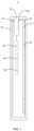
- FIG. 1is a schematic view of a sliding seat received in a receiving space of an electronic apparatus according to a first embodiment of the present disclosure.
- FIG. 2is a schematic view of a sliding seat moving out of a receiving space of an electronic apparatus according to a first embodiment of the present disclosure.
- FIG. 3is a schematic view of a sliding seat moved out from a receiving space and a middle frame of an electronic apparatus according to a first embodiment of the present disclosure.
- the electronic apparatusmay include but not limited to smartphone, mobile internet device (MID), electronic book, Play Station Portable (PSP) and Personal Digital Assistant (PDA) or other communication devices.
- MIDmobile internet device
- PSPPlay Station Portable
- PDAPersonal Digital Assistant
- the electronic apparatus 1may include a main body 10, a sliding seat 20 a middle frame 30 and four first antenna radiators T11.
- the main body 10may have a receiving space 14 defined therein.
- An opening 10amay be formed on the main body 10 to communicate with the receiving space 14 such that the receiving space 14 may be communicated outside via the opening 10a.
- the sliding seat 20may be received in the receiving space 14 and movably connected to the main body 10 through the opening 10a such that the sliding seat 20 may have a capability of being moved out from or retracted into the receiving space 14 via the opening 10a.
- the middle frame 30may be received in the receiving space 14.
- Four first antenna radiators T11may be disposed on the middle frame 30 and the sliding seat 20. The four first antenna radiators T11 can have a capability of operating at a first frequency band.
- four first antenna radiators T11may be disposed on the middle frame 30 and the sliding seat 20.
- the four first antenna radiators T11can form a 4*4 MIMO antenna array to greatly improve the performance of the antenna.
- part of the four first antenna radiators T11since part of the four first antenna radiators T11 may be disposed on the sliding seat 20, when the sliding seat 20 is moved out from the main body 10, the part of the four first antenna radiators T11 can be away from the main body 10 to effectively enlarge the clearance area of the part of the four first antenna radiators T11, from which the performance of the antenna and the communication effect of the electronic apparatus 1 can be improved.
- the middle frame 30may include a first portion 310 and a second portion 320.
- the first portion 310 and the second portion 320may be arranged to be opposite to each other.
- the first portion 310may be located closer to the opening 10a than the second portion 320.
- One of the four first antenna radiators T11may be disposed on the sliding seat 20.
- Another of the four first antenna radiators T11may be disposed on the first portion 310.
- other two of the four first antenna radiators T11may be disposed on the second portion 320.
- first antenna radiators T11 of the four first antenna radiators T11may further have a capability of operating at a second frequency band.
- one of the two first antenna radiators T11 further having a capability of operating at the second frequency bandmay be disposed on the first portion 310, the other one of the two first antenna radiators T11 may be disposed on the second portion 320.
- the four first antenna radiators T11may form a 4*4 Multiple Input and Multiple Output (MIMO) Long Term Evolution (LTE; the 4 generation communication network system) antenna array.
- the first frequency bandmay include an intermediate frequency band and a high frequency band of LTE frequency band.
- the intermediate frequency band of LTE frequency bandcan be in a range of 1710MHz ⁇ 2170MHz
- the high frequency band of LTE frequency bandcan be in a range of 2300MHz ⁇ 2400MHz and 2500MHz ⁇ 2700MHz.
- the second frequency bandmay include a low frequency band of LTE frequency band. Wherein the low frequency band of LTE frequency band can be in a range of 824MHz ⁇ 960MHz.
- the electronic apparatusmay further include at least two second antenna radiators T12 disposed on the middle frame 30.
- the at least two second antenna radiators T12can have a capability of operating at a third frequency band.
- the at least two second antenna radiators T12may be disposed on the first portion 320.
- the third frequency bandmay be a 5G Wi-Fi frequency band.
- the at least two second antenna radiators T12can form a 2*2MIMO 5G Wi-Fi antenna array.
- a range of the 5G Wi-Fi frequency bandmay generally be 5.1 GHz ⁇ 5.8GHz.
- the electronic apparatus 1may further include a third antenna radiator T13 disposed on the sliding seat 20.
- the third antenna radiator T13can have a capability of operating at a fourth frequency band.
- the fourth frequency bandmay include a 2.4G Wi-Fi frequency band.
- the 2.4G Wi-Fi frequency bandmay generally be in a range of 2.4GHz ⁇ 2.5GHz.
- the sliding seat 20may be made of a metal material.
- Each of the first antenna radiator T11 and the third antenna radiator T13 disposed on the sliding seat 20may be an independent metal area of the sliding seat 20 separated by slot bands.
- the middle frame 30may be made of a metal material.
- Each first antenna radiator T11 disposed on the middle frame 30may be an independent metal area of the middle frame 30 separated by a slot band.
- One second antenna radiator T12 disposed on the middle frame 30may be an independent metal area of the middle frame 30 separated by a slot band.
- Another second antenna radiator T12 disposed on the middle frame 30may be a FPC antenna fixed on the middle frame 30.
- the sliding seat 20can be made of an insulating material.
- the first antenna radiator T11 and the third antenna radiator T13 disposed on the sliding seat 20may be FPC antennas fixed on the sliding seat 20, or LDS antennas respectively formed on the sliding seat 20 by laser engraving, or PDS antennas formed on the sliding seat 20 by printing.
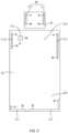
- FIG. 4is a schematic diagram of an electronic apparatus 1 according to the second embodiment of the present disclosure.
- the main body 10may include a display screen 110 and a battery cover 120.
- the battery cover 120may include a bezel 121 and a cover plate 122 fixed to the bezel 121.
- the display screen 110 and the cover plate 122may be arranged on two opposite sides of the bezel 121 respectively.
- the receiving space 14can be defined by the cover plate 122, the bezel 121 and the display screen 110.
- the opening 10amay be formed in the bezel 121.
- the display screen 110can be a liquid crystal display panel, an organic light emitting diode display panel and so on.
- the display screen 110may be either a display panel with a single display function or a display panel integrating a touch screen function.
- FIG. 5is a schematic diagram of an electronic apparatus according to a third embodiment of the present disclosure.
- the main body 10may include a display screen 110 and a battery cover 120.
- the battery cover 120may include a bezel 121 and a cover plate 122 fixed to the bezel 121.
- the display screen 110 and the cover plate 122may be arranged on two opposite sides of the bezel 121 respectively.
- the receiving space 14can be defined by the cover plate 122, the bezel 121 and the display screen 110.
- the opening 10amay be defined on the bezel 121 and pass through a part of the cover plate 122.
- the electronic apparatus 1may further include a driving mechanism 40.
- the sliding seat 20can be moved out from or retracted into the receiving space 14 by the driving mechanism 40.
- the driving mechanism 40may be connected to one end of the sliding seat 20.
- the driving mechanism 40can send out a driving signal, drove by which the sliding seat 20 can be moved out from or retracted into the receiving space 14.
- the driving mechanism 40may be a driving motor, or can also undergo an enlongation or a contraction through a gear and rack.
- the driving mechanism 40may also be made of electrostrictive material. When the driving mechanism 40 loads a first electrical signal, the electrostrictive material can elongate to drive the sliding seat 20 to be moved out from the receiving space 14. When the driving mechanism 40 loads a second electrical signal, the electrostrictive material can contract to drive the sliding seat 20 to be retracted into the receiving space 14. A polarity of the first electrical signal may be different from that of the second electrical signal.
- the driving mechanism 40may be made of magnetostrictive material.
- the driving mechanism 40may include a drive lever and a coil wound around an outer peripheral surface of the drive lever.
- the coilloads a third electrical signal, it may generate a first electromagnetic wave signal.
- the drive levercan elongate to drive the sliding seat 20 to be moved out from the receiving space 14.
- the coilloads a fourth electrical signal, it may generate a second electromagnetic wave signal.
- the drive leverUnder an effect of the second electromagnetic wave signal, the drive lever can contract to drive the sliding seat 20 to be retracted into the receiving space 14.
- a winding direction of the coil wound around the outer peripheral surface of the drive leverremains unchanged, a flow direction of the third electrical signal is different from that of the fourth electrical signal.
- the electronic apparatus 1may further include at least one function module 50 mounted on the sliding seat.
- the function module 50may be selected from a group including a camera module, a flash lamp module, a position sensor module and a receiver module. Since the function module 50 can be mounted on the sliding seat 20 to be moved out from the receiving space 14 along with the sliding seat 20, there is no need to define a corresponding hole to receive the function module 50 on a non-display area of the display screen 110, which can improve a proportion of a display area, in favor of achieving a full screen of the electronic apparatus 1.
- the electronic apparatus 1further includes a frequency offset corrector 60 configured to correct a frequency offset of any antenna radiator near the sliding seat 20 caused by a position change of the sliding seat 20 relative to the main body 10.
- the electronic apparatus 1may further include a selector 70.
- the selector 70may be configured to select a first antenna radiator T11 disposed on the middle frame 30 or a first antenna radiator T11 disposed on the sliding seat 20 to work, when the sliding seat 20 is received in the receiving space 14.
- FIG. 6is a schematic diagram of the sliding seat of an electronic apparatus according to a fourth embodiment.
- FIG. 7is a schematic diagram of the sliding seat provided by FIG. 4 moving out of the receiving space.
- FIG. 8is a schematic diagram of the sliding seat provided by FIG. 4 received in the receiving space.
- the sliding seat 20can be made of a metal material or an insulating material.
- the sliding seat 20may include a seat body 220 and a lid portion 210.
- the seat body 220 and the lid portion 210may be connected to each other by a side face of the seat body 220 and a side face of the lid portion 210.
- a size of the lid portion 210 along a direction perpendicular to a removal direction of the sliding seat 20is larger than a size of the sliding seat 20 along the direction perpendicular to a removal direction of the sliding seat 20.
- the lid portion 210may include a first connection face 21 0a, a first surface 210b, a second surface 210c and a third surface 210d.
- the first connection face 210ais a face facing to the seat body 220.
- the first surface 210bmay be located opposite to the first connection face 210a.
- the second surface 210cmay be located opposite to the third surface 210d.
- the second surface 210cmay be connected to the first connection face 210a and the first surface 210b.
- the third surface 210cmay be connected to the first connection face 210a and the first surface 210b.
- the seat body 220may include a second connection face 220a facing to the lid portion 210.
- the seat body 220may further include a fourth surface 220b and a fifth surface 220c which are located opposite to each other.
- the second connection face 220amay be connected to the fourth surface 220b and the fifth surface 220c.
- the seat body 220 and the lid portion 210 connected to each other by a side face of the seat body 220 and a side face of the lid portion 210may mean a plane the fourth surface 220b lies in may be located between a plane the second surface 210c lies in and a plane the third surface 210d lies in, and a plane the fifth surface 220c lies in may be located between the plane the second surface 210c and the plane the third surface 210d lies in.
- the first antenna radiator T11 and the third antenna radiator T13may be disposed on the seat body 220, and the seat body 220 and the lid portion 210 may be connected to each other by a side face of the seat body 220 and a side face of the lid portion 210.
- An inner wall of the opening 10acan have a reasonable distance to the first antenna radiator T11 and the third antenna radiator T13, which can decrease damage to antenna radiators disposed on the seat body 220, while the sliding seat 20 is moved out of or retracted into the receiving space 14.
- the size of the lid portion 210 along the direction perpendicular to the removal direction of the sliding seat 20is larger than the size of the sliding seat 20 along the direction perpendicular to the removal direction of the sliding seat 20, sealing performance of the electronic apparatus 1 can be enhanced while the sliding seat 20 is received in the receiving space 14, which can reduce entrance of dust and the like into the receiving space 14.
- the lid portion 210is movably connected to the seat body 220.
- the lid portion 210can move in a predetermined distance relative to the seat body 220 in a plane defined by the first surface 210b of the lid portion 210. Due to assembly errors, the lid portion 210 may touch side walls of the main body 10 configured to define the opening 10a, while the sliding seat 20 is moved out of or retracted into the receiving space 14 through the opening 10a. Since the lid portion 210 can move in a predetermined distance relative to the seat body 220 in a plane defined by the first surface 210b of the lid portion 210, the lid portion 210 can not be blocked by the side walls. Thus, the sliding seat 20 can be moved out of or retracted into the receiving space 14 more smoothly.
- FIGS. 1-3illustrate an electronic apparatus of an embodiment according to the present disclosure.
- the electronic apparatus 1may include a housing 10, a sliding seat 20 and a plurality of antenna 80 radiators.
- the housing 10may have a receiving space 14 defined therein. Wherein an opening 10a may be formed in the housing 10 to communicate with the receiving space 14 such that the receiving space 14 can be communicated outside via the opening 10a.
- the sliding seat 20may be received in the receiving space 14, and movably connected to the housing 10 such that the sliding seat 20 can have a capability of being moved out from or retracted into the receiving space 14 via the opening 10a.
- a plurality of antenna 80 radiatorsmay be disposed on the sliding seat 20 and configured to be moved out from or retracted into the receiving space 14 along with the sliding seat 20.
- FIGS. 1-3illustrate a smartphone of an embodiment according to the present disclosure.
- the smartphone 1may include a housing 10, a sliding seat 20 and a plurality of antenna 80 radiators.
- the housing 10may have a receiving space 14 defined therein. Wherein an opening 10a may be formed in the housing 10 to communicate with the receiving space 14 such that the receiving space 14 can be communicated outside via the opening 10a.
- the housing 10may include a display screen 110, a bezel 121, and a cover plate 122.
- the cover plate 122may be fixed to the bezel 121.
- the display screen 110 and the cover plate 122may be arranged on two opposite sides of the bezel 121 respectively.
- the receiving space 14may be defined by the cover plate 122, the bezel 121 and the display screen 110.
- the opening 10amay be formed in the bezel 121.
- the sliding seat 20may be received in the receiving space 14 and movably connected to the housing 10 such that the sliding seat 20 can have a capability of being moved out from or retracted into the receiving space 14 via the opening 10a.
- a plurality of antenna 80 radiatorsmay be disposed on the sliding seat 20 and configured to be moved out from or retracted into the receiving space 14 along with the sliding seat 20.
Landscapes
- Engineering & Computer Science (AREA)
- Signal Processing (AREA)
- Computer Networks & Wireless Communication (AREA)
- Telephone Set Structure (AREA)
- Details Of Aerials (AREA)
- Support Of Aerials (AREA)
Description
- The described embodiments relate to electronic technology, and in particular to an electronic apparatus.
- Antenna is a convertor, which can convert guided wave transmitted on transmission line to electromagnetic wave transmitted on unbounded medium (generally free space), or convert electromagnetic wave transmitted on unbounded medium to guided wave transmitted on transmission line. Electronic apparatus such as mobile phone usually include antenna to achieve communication function. However, along with the recent trend towards thinness on the electronic apparatus, such as mobile phone, receiving space in the electronic apparatus is smaller and smaller, causing clearance area in the electronic apparatus narrower and narrower, which results in a poor communication effect.
- US patent application
US 2007/0035454 A1 provides a system and apparatus for an extendable antenna architecture. The apparatus may include an antenna body having one or more antenna traces, and an antenna housing to couple to the antenna body. The antenna housing may have an extended position and a retracted position. The antenna housing may have a first external surface forming a substantially continuous plane with a second external surface for a device housing when in the retracted position. Other embodiments are described and claimed. - US patent
US 8477074 B2 provides a card-type device. A slide antenna board is slidably provided between a state in which slide antenna board is accommodated in a card body and a state in which slide antenna board is pulled out from the card body. The slide antenna board includes a planar type antenna. A base end side of a rod antenna is fixed to the card body and an extended side of the rod antenna is slidably and stretchably disposed in a slide direction of the slide antenna board through a slide guide in the slide antenna board. A leading end surface of rod antenna is not projected ahead of a leading end surface of slide antenna board in a state in which the rod antenna is accommodated. An engagement unit engaging the slide antenna board is provided with the leading end side of the rod antenna. The rod antenna engaging slide antenna board is configured to be pulled out together with the slide antenna board while the slide antenna board is pulled out from the card body. - Chinese patent application
CN102118464A provides a portable electronic device, comprising a shell, a telescopic component and a processing module, wherein the telescopic component is arranged on the shell and comprises a flashing light module and an antenna; the antenna is used for receiving a signal; when the processing module executes an application program, the processing module drives the telescopic component to pop up, so that the flashing light module and the antenna move to an exposed position outside the shell from a hidden position inside the shell. - The present disclosure provides an electronic apparatus according to
claim 1. - Compared to related art, in the electronic apparatus of the present disclosure, four first antenna radiators may be disposed on the middle frame and the sliding seat. The four first antenna radiators can form a 4*4 MIMO antenna to greatly improve the performance of the antenna. What's more, since part of the four first antenna radiators may be disposed on the sliding seat, when the sliding seat is removed from the main body, the part of the four first antenna radiators can be away from the main body to effectively enlarge the clearance area of the part of the four first antenna radiators, from which the performance of the antenna and the communication effect of the electronic apparatus can be improved.
- Accompanying drawings are for providing further understanding of embodiments of the present disclosure. The drawings form a part of the disclosure and are for illustrating the principle of the embodiments of the present disclosure along with the literal description. Apparently, the drawings in the description below are merely some embodiments of the present disclosure, a person skilled in the art can obtain other drawings according to these drawings without creative efforts.
FIG. 1 is a schematic view of a sliding seat received in a receiving space of an electronic apparatus according to a first embodiment of the present disclosure.FIG. 2 is a schematic view of a sliding seat moving out of a receiving space of an electronic apparatus according to a first embodiment of the present disclosure.FIG. 3 is a schematic view of a sliding seat moved out from a receiving space and a middle frame of an electronic apparatus according to a first embodiment of the present disclosure.FIG. 4 is a schematic diagram of an electronic apparatus according to a second embodiment of the present disclosure.FIG. 5 is a schematic diagram of an electronic apparatus according to a third embodiment of the present disclosure.FIG. 6 is a schematic diagram of the sliding seat of an electronic apparatus according to a fourth embodiment of the present disclosure.FIG. 7 is a schematic diagram of the sliding seat provided byFIG. 4 moving out of the receiving space.FIG. 8 is a schematic diagram of the sliding seat provided byFIG. 4 received in the receiving space.- In order to be more clearly understood, the above objects, features and advantages of the present disclosure will be described with reference to drawings and embodiments in detail hereinbelow. Note that combination of different embodiments and features are allowable as long as they do not conflict to each other.
- An electronic apparatus according to an embodiment of the present disclosure may include a main body, a middle frame, a sliding seat and four first antenna radiators. The main body may have a receiving space defined therein. An opening may be formed in the main body to communicate with the receiving space such that the receiving space can be communicated outside via the opening. The sliding seat may be received in the receiving space and movably connected to the main body such that the sliding seat may have a capability of being moved out from or retracted into the receiving space via the opening. The middle frame may be received in the receiving space. Four first antenna radiators may be disposed on the middle frame and the sliding seat respectively. The four first antenna radiators may have a capability of operating at a first frequency band.
- In another embodiment, the middle frame may include a first portion and a second portion. The first portion and the second portion may be arranged to be opposite to each other. The first portion may be located closer to the opening than the second portion. One of the four first antenna radiators may be disposed on the sliding seat. Another one of the four first antenna radiators may be disposed on the first portion. Another two of the four first antenna radiators may be disposed on the second portion.
- In another embodiment, two first antenna radiators of the four first antenna radiators may further have a capability of operating at a second frequency band.
- In further another embodiment, one of the two first antenna radiators further having a capability of operating at the second frequency band may be disposed on the first portion. The other one of the two first antenna radiators may be disposed on the second portion.
- In still further another embodiment, the four first antenna radiators may form a 4*4 MIMO LTE antenna array. The first frequency band may be an intermediate frequency band and a high frequency band of LTE frequency band. The intermediate frequency band of the LTE frequency band may be in a range of 1710MHZ~2170MHZ. The high frequency band of the LTE frequency band may be in a range of 2300MHZ∼2400MHZ and 2500MHZ~2700MHZ.
- In one embodiment, the second frequency band may include a low frequency band of LTE frequency band. The low frequency band of the LTE frequency band may be in a range of 824MHz~960MHz.
- In another embodiment, the electronic apparatus may further include at least two second antenna radiators disposed on the middle frame. The at least two second antenna radiators may have a capability of operating at a third frequency band.
- In another embodiment, the middle frame may include a first portion and a second portion. The first portion and the second portion may be arranged to be opposite to each other. The first portion may be located closer to the opening than the second portion. The at least two second antenna radiators may be disposed on the first portion.
- In another embodiment, the third frequency band may be a 5G Wi-Fi frequency band. The at least two second antenna radiators may form a 2*2MIMO 5G Wi-Fi antenna array.
- In further another embodiment, the middle frame may be made of metal. Each first antenna radiator disposed on the middle frame may be an independent metal area of the middle frame separated by a slot band.
- In further another embodiment, one second antenna radiator disposed on the middle frame may be an independent metal area of the middle frame separated by a slot band. Another second antenna radiator disposed on the middle frame may be a FPC antenna fixed on the middle frame.
- In still further another embodiment, the electronic apparatus may further include a third antenna radiator disposed on the sliding seat. The third antenna radiator may have a capability of operating at a fourth frequency band. The fourth frequency band may include a 2.4G Wi-Fi frequency band.
- In one embodiment, the sliding seat may be made of an insulating material. The first antenna radiator and the third antenna radiator disposed on the sliding seat may be FPC antennas fixed on the sliding seat, or LDS antennas formed on the sliding seat by laser engraving, or PDS antennas formed on the sliding seat by printing.
- In another embodiment, the sliding seat may be made of metal. Each of the first antenna radiator and the third antenna radiator disposed on the sliding seat may be an independent metal area of the sliding seat separated by slot bands.
- In another embodiment, the main body may include a display screen and a battery cover. The battery cover may include a bezel and a cover plate. The cover plate may be fixed to the bezel. The display screen and the cover plate may be arranged on two opposite sides of the bezel respectively. The receiving space may be defined by the cover plate, the bezel and the display screen. The opening may be formed in the bezel.
- In further another embodiment, the opening may be formed in the bezel and further pass through a part of the cover plate.
- In further another embodiment, the electronic apparatus may further include a driving mechanism to drive the sliding seat to be moved out from or retracted into the receiving space.
- In further another embodiment, the electronic apparatus may further include at least one function module. The function module may be selected from a group including a camera module, a flash lamp module, a position sensor module and a receiver module. The function module may be mounted on the sliding seat.
- According to the invention, the electronic apparatus further includes a frequency offset corrector. The frequency offset corrector may be configured to correct a frequency offset of any antenna radiator near the sliding seat caused by a position change of the sliding seat relative to the main body.
- In one embodiment, the electronic apparatus may further include a selector. The selector may be configured to select a first antenna radiator disposed on the middle frame or a first antenna radiator disposed on the sliding seat to work, when the sliding seat is received in the receiving space.
- An electronic apparatus according to an embodiment of the present disclosure may include a housing, a sliding seat and a plurality of antenna radiators. The housing may have a receiving space defined therein. Wherein an opening may be formed in the housing to communicate with the receiving space such that the receiving space can be communicated outside via the opening. The sliding seat may be received in the receiving space, and movably connected to the housing such that the sliding seat can have a capability of being moved out from or retracted into the receiving space via the opening. A plurality of antenna radiators may be disposed on the sliding seat and configured to be moved out from or retracted into the receiving space along with the sliding seat.
- A smartphone according to an embodiment of the present disclosure may include a housing, a sliding seat and a plurality of antenna radiators. The housing may have a receiving space defined therein. Wherein an opening may be formed in the housing to communicate with the receiving space such that the receiving space can be communicated outside via the opening. The housing may include a display screen, a bezel, and a cover plate. The cover plate may be fixed to the bezel. The display screen and the cover plate may be arranged on two opposite sides of the bezel respectively. The receiving space may be defined by the cover plate, the bezel and the display screen. The opening may be formed in the bezel. The sliding seat may be received in the receiving space and movably connected to the housing such that the sliding seat can have a capability of being moved out from or retracted into the receiving space via the opening. Wherein a plurality of antenna radiators may be disposed on the sliding seat and configured to be moved out from or retracted into the receiving space along with the sliding seat.
- Please refer to
FIG. 1 ,FIG. 2 andFIG. 3 ,FIG. 1 is a schematic view of a sliding seat received in a receiving space of an electronic apparatus according to a first embodiment of the present disclosure.FIG. 2 is a schematic view of a sliding seat moving out of a receiving space of an electronic apparatus according to a first embodiment of the present disclosure.FIG. 3 is a schematic view of a sliding seat moved out from a receiving space and a middle frame of an electronic apparatus according to a first embodiment of the present disclosure. The electronic apparatus may include but not limited to smartphone, mobile internet device (MID), electronic book, Play Station Portable (PSP) and Personal Digital Assistant (PDA) or other communication devices. - The
electronic apparatus 1 may include amain body 10, a sliding seat 20 amiddle frame 30 and four first antenna radiators T11. Themain body 10 may have a receivingspace 14 defined therein. Anopening 10a may be formed on themain body 10 to communicate with the receivingspace 14 such that the receivingspace 14 may be communicated outside via theopening 10a. The slidingseat 20 may be received in the receivingspace 14 and movably connected to themain body 10 through theopening 10a such that the slidingseat 20 may have a capability of being moved out from or retracted into the receivingspace 14 via theopening 10a. Themiddle frame 30 may be received in the receivingspace 14. Four first antenna radiators T11 may be disposed on themiddle frame 30 and the slidingseat 20. The four first antenna radiators T11 can have a capability of operating at a first frequency band. - Compared to related art, in the
electronic apparatus 1 of the present disclosure, four first antenna radiators T11 may be disposed on themiddle frame 30 and the slidingseat 20. The four first antenna radiators T11 can form a 4*4 MIMO antenna array to greatly improve the performance of the antenna. What's more, since part of the four first antenna radiators T11 may be disposed on the slidingseat 20, when the slidingseat 20 is moved out from themain body 10, the part of the four first antenna radiators T11 can be away from themain body 10 to effectively enlarge the clearance area of the part of the four first antenna radiators T11, from which the performance of the antenna and the communication effect of theelectronic apparatus 1 can be improved. - Further, the
middle frame 30 may include afirst portion 310 and asecond portion 320. Thefirst portion 310 and thesecond portion 320 may be arranged to be opposite to each other. Thefirst portion 310 may be located closer to theopening 10a than thesecond portion 320. One of the four first antenna radiators T11 may be disposed on the slidingseat 20. Another of the four first antenna radiators T11 may be disposed on thefirst portion 310. And other two of the four first antenna radiators T11 may be disposed on thesecond portion 320. - Further, two first antenna radiators T11 of the four first antenna radiators T11 may further have a capability of operating at a second frequency band.
- Further, one of the two first antenna radiators T11 further having a capability of operating at the second frequency band may be disposed on the
first portion 310, the other one of the two first antenna radiators T11 may be disposed on thesecond portion 320. - Further, the four first antenna radiators T11 may form a 4*4 Multiple Input and Multiple Output (MIMO) Long Term Evolution (LTE; the 4 generation communication network system) antenna array. The first frequency band may include an intermediate frequency band and a high frequency band of LTE frequency band. The intermediate frequency band of LTE frequency band can be in a range of 1710MHz~2170MHz, and the high frequency band of LTE frequency band can be in a range of 2300MHz~2400MHz and 2500MHz~2700MHz. The second frequency band may include a low frequency band of LTE frequency band. Wherein the low frequency band of LTE frequency band can be in a range of 824MHz~960MHz.
- Furthermore, the electronic apparatus may further include at least two second antenna radiators T12 disposed on the
middle frame 30. The at least two second antenna radiators T12 can have a capability of operating at a third frequency band. The at least two second antenna radiators T12 may be disposed on thefirst portion 320. The third frequency band may be a 5G Wi-Fi frequency band. The at least two second antenna radiators T12 can form a 2*2MIMO 5G Wi-Fi antenna array. A range of the 5G Wi-Fi frequency band may generally be 5.1 GHz~5.8GHz. - The
electronic apparatus 1 may further include a third antenna radiator T13 disposed on the slidingseat 20. The third antenna radiator T13 can have a capability of operating at a fourth frequency band. The fourth frequency band may include a 2.4G Wi-Fi frequency band. The 2.4G Wi-Fi frequency band may generally be in a range of 2.4GHz~2.5GHz. - In the present embodiment, the sliding
seat 20 may be made of a metal material. Each of the first antenna radiator T11 and the third antenna radiator T13 disposed on the slidingseat 20 may be an independent metal area of the slidingseat 20 separated by slot bands. - The
middle frame 30 may be made of a metal material. Each first antenna radiator T11 disposed on themiddle frame 30 may be an independent metal area of themiddle frame 30 separated by a slot band. - One second antenna radiator T12 disposed on the
middle frame 30 may be an independent metal area of themiddle frame 30 separated by a slot band. Another second antenna radiator T12 disposed on themiddle frame 30 may be a FPC antenna fixed on themiddle frame 30. - In other embodiments, the sliding
seat 20 can be made of an insulating material. The first antenna radiator T11 and the third antenna radiator T13 disposed on the slidingseat 20 may be FPC antennas fixed on the slidingseat 20, or LDS antennas respectively formed on the slidingseat 20 by laser engraving, or PDS antennas formed on the slidingseat 20 by printing. - Hereinbelow, an
electronic apparatus 1 of a second embodiment according to the present disclosure will be described with reference to theelectronic apparatus 1 of the first embodiment described above. Please refer toFIG. 4, FIG. 4 is a schematic diagram of anelectronic apparatus 1 according to the second embodiment of the present disclosure. In this embodiment, themain body 10 may include adisplay screen 110 and abattery cover 120. Thebattery cover 120 may include abezel 121 and acover plate 122 fixed to thebezel 121. Thedisplay screen 110 and thecover plate 122 may be arranged on two opposite sides of thebezel 121 respectively. The receivingspace 14 can be defined by thecover plate 122, thebezel 121 and thedisplay screen 110. Theopening 10a may be formed in thebezel 121. - The
display screen 110 can be a liquid crystal display panel, an organic light emitting diode display panel and so on. Thedisplay screen 110 may be either a display panel with a single display function or a display panel integrating a touch screen function. - Hereinbelow, an
electronic apparatus 1 of a third embodiment according to the present disclosure will be described with reference to theelectronic apparatus 1 of the first embodiment described above. Please refer toFIG. 5, FIG. 5 is a schematic diagram of an electronic apparatus according to a third embodiment of the present disclosure. In this embodiment, themain body 10 may include adisplay screen 110 and abattery cover 120. Thebattery cover 120 may include abezel 121 and acover plate 122 fixed to thebezel 121. Thedisplay screen 110 and thecover plate 122 may be arranged on two opposite sides of thebezel 121 respectively. The receivingspace 14 can be defined by thecover plate 122, thebezel 121 and thedisplay screen 110. Theopening 10a may be defined on thebezel 121 and pass through a part of thecover plate 122. - In one embodiment with reference to the
electronic apparatus 1 according to any embodiment described above, theelectronic apparatus 1 may further include adriving mechanism 40. The slidingseat 20 can be moved out from or retracted into the receivingspace 14 by thedriving mechanism 40. Specifically, thedriving mechanism 40 may be connected to one end of the slidingseat 20. Thedriving mechanism 40 can send out a driving signal, drove by which the slidingseat 20 can be moved out from or retracted into the receivingspace 14. Thedriving mechanism 40 may be a driving motor, or can also undergo an enlongation or a contraction through a gear and rack. Thedriving mechanism 40 may also be made of electrostrictive material. When thedriving mechanism 40 loads a first electrical signal, the electrostrictive material can elongate to drive the slidingseat 20 to be moved out from the receivingspace 14. When thedriving mechanism 40 loads a second electrical signal, the electrostrictive material can contract to drive the slidingseat 20 to be retracted into the receivingspace 14. A polarity of the first electrical signal may be different from that of the second electrical signal. - It will be understood that, in other embodiment, the
driving mechanism 40 may be made of magnetostrictive material. And thedriving mechanism 40 may include a drive lever and a coil wound around an outer peripheral surface of the drive lever. When the coil loads a third electrical signal, it may generate a first electromagnetic wave signal. Under an effect of the first electromagnetic wave signal, the drive lever can elongate to drive the slidingseat 20 to be moved out from the receivingspace 14. When the coil loads a fourth electrical signal, it may generate a second electromagnetic wave signal. Under an effect of the second electromagnetic wave signal, the drive lever can contract to drive the slidingseat 20 to be retracted into the receivingspace 14. When a winding direction of the coil wound around the outer peripheral surface of the drive lever remains unchanged, a flow direction of the third electrical signal is different from that of the fourth electrical signal. - In one embodiment with reference to the
electronic apparatus 1 according to any embodiment described above, theelectronic apparatus 1 may further include at least onefunction module 50 mounted on the sliding seat. Thefunction module 50 may be selected from a group including a camera module, a flash lamp module, a position sensor module and a receiver module. Since thefunction module 50 can be mounted on the slidingseat 20 to be moved out from the receivingspace 14 along with the slidingseat 20, there is no need to define a corresponding hole to receive thefunction module 50 on a non-display area of thedisplay screen 110, which can improve a proportion of a display area, in favor of achieving a full screen of theelectronic apparatus 1. - In embodiments according to the invention, the
electronic apparatus 1 further includes a frequency offsetcorrector 60 configured to correct a frequency offset of any antenna radiator near the slidingseat 20 caused by a position change of the slidingseat 20 relative to themain body 10. - In one embodiment with reference to the
electronic apparatus 1 according to any embodiment described above, theelectronic apparatus 1 may further include aselector 70. Theselector 70 may be configured to select a first antenna radiator T11 disposed on themiddle frame 30 or a first antenna radiator T11 disposed on the slidingseat 20 to work, when the slidingseat 20 is received in the receivingspace 14. - Referring to
FIGS. 6-8 ,FIG. 6 is a schematic diagram of the sliding seat of an electronic apparatus according to a fourth embodiment.FIG. 7 is a schematic diagram of the sliding seat provided byFIG. 4 moving out of the receiving space.FIG. 8 is a schematic diagram of the sliding seat provided byFIG. 4 received in the receiving space. In this embodiment, the slidingseat 20 can be made of a metal material or an insulating material. The slidingseat 20 may include aseat body 220 and alid portion 210. Theseat body 220 and thelid portion 210 may be connected to each other by a side face of theseat body 220 and a side face of thelid portion 210. A size of thelid portion 210 along a direction perpendicular to a removal direction of the slidingseat 20 is larger than a size of the slidingseat 20 along the direction perpendicular to a removal direction of the slidingseat 20. When the sliding seat 2 is received in the receivingspace 14, a face of thelid portion 210 away from the slidingseat 20 can form part of a facade of theelectronic apparatus 1. The first antenna radiator T11 and the third antenna radiator T13 may be disposed on theseat body 220. - Specifically, the
lid portion 210 may include a first connection face 21 0a, afirst surface 210b, asecond surface 210c and a third surface 210d. Thefirst connection face 210a is a face facing to theseat body 220. Thefirst surface 210b may be located opposite to thefirst connection face 210a. When the slidingseat 20 is received in the receivingspace 14, thefirst surface 210b can form part of a facade of theelectronic apparatus 1. Thesecond surface 210c may be located opposite to the third surface 210d. Thesecond surface 210c may be connected to thefirst connection face 210a and thefirst surface 210b. Thethird surface 210c may be connected to thefirst connection face 210a and thefirst surface 210b. Theseat body 220 may include asecond connection face 220a facing to thelid portion 210. Theseat body 220 may further include afourth surface 220b and afifth surface 220c which are located opposite to each other. Thesecond connection face 220a may be connected to thefourth surface 220b and thefifth surface 220c. Theseat body 220 and thelid portion 210 connected to each other by a side face of theseat body 220 and a side face of thelid portion 210 may mean a plane thefourth surface 220b lies in may be located between a plane thesecond surface 210c lies in and a plane the third surface 210d lies in, and a plane thefifth surface 220c lies in may be located between the plane thesecond surface 210c and the plane the third surface 210d lies in. - In this embodiment, the first antenna radiator T11 and the third antenna radiator T13 may be disposed on the
seat body 220, and theseat body 220 and thelid portion 210 may be connected to each other by a side face of theseat body 220 and a side face of thelid portion 210. An inner wall of theopening 10a can have a reasonable distance to the first antenna radiator T11 and the third antenna radiator T13, which can decrease damage to antenna radiators disposed on theseat body 220, while the slidingseat 20 is moved out of or retracted into the receivingspace 14. Further, since the size of thelid portion 210 along the direction perpendicular to the removal direction of the slidingseat 20 is larger than the size of the slidingseat 20 along the direction perpendicular to the removal direction of the slidingseat 20, sealing performance of theelectronic apparatus 1 can be enhanced while the slidingseat 20 is received in the receivingspace 14, which can reduce entrance of dust and the like into the receivingspace 14. - Furthermore, according to the invention, the
lid portion 210 is movably connected to theseat body 220. Thelid portion 210 can move in a predetermined distance relative to theseat body 220 in a plane defined by thefirst surface 210b of thelid portion 210. Due to assembly errors, thelid portion 210 may touch side walls of themain body 10 configured to define theopening 10a, while the slidingseat 20 is moved out of or retracted into the receivingspace 14 through theopening 10a. Since thelid portion 210 can move in a predetermined distance relative to theseat body 220 in a plane defined by thefirst surface 210b of thelid portion 210, thelid portion 210 can not be blocked by the side walls. Thus, the slidingseat 20 can be moved out of or retracted into the receivingspace 14 more smoothly. FIGS. 1-3 illustrate an electronic apparatus of an embodiment according to the present disclosure. Theelectronic apparatus 1 may include ahousing 10, a slidingseat 20 and a plurality ofantenna 80 radiators. Thehousing 10 may have a receivingspace 14 defined therein. Wherein anopening 10a may be formed in thehousing 10 to communicate with the receivingspace 14 such that the receivingspace 14 can be communicated outside via theopening 10a. The slidingseat 20 may be received in the receivingspace 14, and movably connected to thehousing 10 such that the slidingseat 20 can have a capability of being moved out from or retracted into the receivingspace 14 via theopening 10a. A plurality ofantenna 80 radiators may be disposed on the slidingseat 20 and configured to be moved out from or retracted into the receivingspace 14 along with the slidingseat 20.FIGS. 1-3 illustrate a smartphone of an embodiment according to the present disclosure. Thesmartphone 1 may include ahousing 10, a slidingseat 20 and a plurality ofantenna 80 radiators. Thehousing 10 may have a receivingspace 14 defined therein. Wherein anopening 10a may be formed in thehousing 10 to communicate with the receivingspace 14 such that the receivingspace 14 can be communicated outside via theopening 10a. Thehousing 10 may include adisplay screen 110, abezel 121, and acover plate 122. Thecover plate 122 may be fixed to thebezel 121. Thedisplay screen 110 and thecover plate 122 may be arranged on two opposite sides of thebezel 121 respectively. The receivingspace 14 may be defined by thecover plate 122, thebezel 121 and thedisplay screen 110. Theopening 10a may be formed in thebezel 121. The slidingseat 20 may be received in the receivingspace 14 and movably connected to thehousing 10 such that the slidingseat 20 can have a capability of being moved out from or retracted into the receivingspace 14 via theopening 10a. Wherein a plurality ofantenna 80 radiators may be disposed on the slidingseat 20 and configured to be moved out from or retracted into the receivingspace 14 along with the slidingseat 20.- What's more, the embodiments described above are only description of the present disclosure, and not intended to limit the scope of the present disclosure. Any equivalent structures that are made according to the specification and the attached drawings of the present disclosure, or any direct or indirect applications of the present disclosure in other related technical fields shall all be covered within the scope of the present disclosure as long as said structures fall within the scope of the appended claims.
Claims (15)
- An electronic apparatus, comprising:a main body (10), having a receiving space (14) defined therein, wherein an opening (10a) is formed in the main body (10) to communicate with the receiving space (14) such that the receiving space (14) is communicatable outside via the opening (10a);a sliding seat (20), received in the receiving space (14), and movably connected to the main body (10) such that the sliding seat (20) has a capability of being moved out from or retracted into the receiving space (14) via the opening (10a);a middle frame (30), received in the receiving space (14); andfour first antenna radiators (T11), wherein three of the four first antenna radiators (T11) are disposed on the middle frame (30) and one of the four first antenna radiators (T11) is disposed on the sliding seat (20) respectively, wherein the four first antenna radiators (T11) have a capability of operating in a first frequency band;characterized in that the electronic apparatus further comprises a frequency offset corrector (60), wherein the frequency offset corrector (60) is configured to correct a frequency offset of any antenna radiator near the sliding seat (20) caused by a position change of the sliding seat (20) relative to the main body (10);the sliding seat (20) includes a seat body (220) and a lid portion (210), the seat body (220) and the lid portion (210) are connected to each other by a side face of the seat body (220) and a side face of the lid portion (210); the lid portion (210) includes a first surface (210b), when the sliding seat (20) is received in the receiving space (14), the first surface (210b) forms a part of a facade of the electronic apparatus (1); the lid portion (210) is movably connected to the seat body (220), the lid portion (210) has a capability of moving in a predetermined distance relative to the seat body (220) in a plane defined by the first surface (210b) of the lid portion (210).
- The electronic apparatus of claim 1, wherein the middle frame (30) comprises a first portion (310) and a second portion (320) which are arranged to be opposite to each other, the first portion (310) is located closer to the opening (10a) than the second portion (320),
one of the three of the four first antenna radiators (T11) is disposed on the first portion (310), and other two of the three of the four first antenna radiators (T11) are disposed on the second portion (320). - The electronic apparatus of claim 2, wherein two of the four first antenna radiators (T11) further have a capability of operating at a second frequency band, the second frequency band comprises a low frequency band of LTE frequency band, the low frequency band of the LTE frequency band is in a range of 824MHz-960MHz.
- The electronic apparatus of claim 3, wherein one of the two first antenna radiators (T11) having a capability of operating at the second frequency band is disposed on the first portion (310), the other one of the two first antenna radiators (T11) is disposed on the second portion (320).
- The electronic apparatus of claim 1, further comprising at least two second antenna radiators (T12) disposed on the middle frame (30), wherein the at least two second antenna radiators (T12) has a capability of operating at a third frequency band, the third frequency band is a 5GHz Wi-Fi frequency band, the at least two second antenna radiators (T12) form a 2*2MIMO 5GHz Wi-Fi antenna array.
- The electronic apparatus of claim 5, wherein the middle frame (30) comprises a first portion (310) and a second portion (320) which are arranged to be opposite to each other, the first portion (310) is located closer to the opening (10a) than the second portion (320), the at least two second antenna radiators (T12) are disposed on the first portion (310).
- The electronic apparatus of claim 5, wherein the middle frame (30) is made of a metal material, each first antenna radiator (T11) disposed on the middle frame (30) is an independent metal area of the middle frame (30) separated by a slot band formed in the independent metal area.
- The electronic apparatus of claim 7, wherein one second antenna radiator (T12) disposed on the middle frame (30) is an independent metal area of the middle frame (30) separated by a slot band formed in the independent metal area, another second antenna radiator (T12) disposed on the middle frame (30) is a FPC antenna fixed on the middle frame (30).
- The electronic apparatus of claim 1, further comprising a third antenna radiator (T13) disposed on the sliding seat (20), the third antenna radiator (T13) has a capability of operating at a fourth frequency band, the fourth frequency band comprises a 2.4GHz Wi-Fi frequency band.
- The electronic apparatus of claim 9, wherein the sliding seat (20) is made of an insulating material, the first antenna radiator (T11) and the third antenna radiator (T13) disposed on the sliding seat (20) are FPC antennas respectively fixed on the sliding seat (20), or LDS antennas respectively formed on the sliding seat (20) by laser engraving, or PDS antennas formed on the sliding seat (20) by printing.
- The electronic apparatus of claim 9, wherein the sliding seat (20) is made of a metal material, each of the first antenna radiator (T11) and the third antenna radiator (T13) disposed on the sliding seat (20) is an independent metal area of the sliding seat (20) separated by slot bands.
- The electronic apparatus of any claims of claim 1, wherein the four first antenna radiators (T11) form a 4*4 MIMO LTE antenna array, the first frequency band comprises an intermediate frequency band and a high frequency band of LTE frequency band, the intermediate frequency band of the LTE frequency band is in a range of 1710MHz-2170MHz, and the high frequency band of the LTE frequency band is in a range of 2300-2400MHz and 2500-2700MHz.
- The electronic apparatus of claim 1, wherein the main body (10) comprises:a display screen (110); anda battery cover (120), comprising:a bezel (121); anda cover plate (122) fixed to the bezel (121);wherein the display screen (110) and the cover plate (122) are arranged on two opposite sides of the bezel (121) respectively, the receiving space (14) is defined by the cover plate (122), the bezel (121) and the display screen (110), the opening (10a) is formed in the bezel (121).
- The electronic apparatus of claim 13, wherein the opening (10a) further passes through a part of the cover plate (122).
- The electronic apparatus of claim 1, further comprising a driving mechanism (40), at least one function module (50) and a selector (70), wherein driving mechanism (40) is configured to drive the sliding seat (20) to be moved out from or retracted into the receiving space (14), the at least one function module (50) is selected from a group comprising a camera module, a flash lamp module, a position sensor module and a receiver module, and mounted on the sliding seat (20), and the selector (70) is configured to select a first antenna radiator (T11) disposed on the middle frame (30) or a first antenna radiator (T11) disposed on the sliding seat (20) to work, when the sliding seat (20) is received in the receiving space (14).
Applications Claiming Priority (1)
| Application Number | Priority Date | Filing Date | Title |
|---|---|---|---|
| CN201810402824.XACN110416685B (en) | 2018-04-28 | 2018-04-28 | electronic device |
Publications (2)
| Publication Number | Publication Date |
|---|---|
| EP3561950A1 EP3561950A1 (en) | 2019-10-30 |
| EP3561950B1true EP3561950B1 (en) | 2023-04-26 |
Family
ID=66217952
Family Applications (1)
| Application Number | Title | Priority Date | Filing Date |
|---|---|---|---|
| EP19169861.2AActiveEP3561950B1 (en) | 2018-04-28 | 2019-04-17 | Electronic apparatus |
Country Status (4)
| Country | Link |
|---|---|
| US (1) | US10931001B2 (en) |
| EP (1) | EP3561950B1 (en) |
| CN (1) | CN110416685B (en) |
| WO (1) | WO2019206222A1 (en) |
Families Citing this family (5)
| Publication number | Priority date | Publication date | Assignee | Title |
|---|---|---|---|---|
| CN110875513B (en)* | 2018-08-31 | 2022-04-12 | 深圳富泰宏精密工业有限公司 | Wireless communication device |
| CN110011071A (en)* | 2018-12-28 | 2019-07-12 | 瑞声科技(新加坡)有限公司 | Mobile terminal antenna system, mobile terminal |
| CN111641737B (en)* | 2020-04-30 | 2021-06-04 | 广东长盈精密技术有限公司 | Middle frame processing method |
| US20220223997A1 (en)* | 2021-01-13 | 2022-07-14 | Zebra Technologies Corporation | User-Installable Wireless Communications Module |
| CN113176810B (en)* | 2021-04-12 | 2023-04-14 | 维沃移动通信有限公司 | Electronic equipment |
Citations (2)
| Publication number | Priority date | Publication date | Assignee | Title |
|---|---|---|---|---|
| US20100279747A1 (en)* | 2008-01-10 | 2010-11-04 | Panasonic Corporation | Portable radio device |
| EP3547444A2 (en)* | 2018-03-31 | 2019-10-02 | Guangdong Oppo Mobile Telecommunications Corp., Ltd. | Electronic device |
Family Cites Families (22)
| Publication number | Priority date | Publication date | Assignee | Title |
|---|---|---|---|---|
| US6204818B1 (en)* | 2000-02-01 | 2001-03-20 | Auden Technology Mfg. Co., Ltd. | Stretchable antenna for mobile phones |
| KR100629878B1 (en)* | 2004-10-23 | 2006-09-29 | 엘지전자 주식회사 | Mobile communication terminal |
| CN1913227B (en)* | 2005-08-10 | 2013-07-03 | 启碁科技股份有限公司 | monopole antenna |
| US7262737B2 (en)* | 2005-08-15 | 2007-08-28 | Palm, Inc. | Extendable antenna architecture |
| CN2874800Y (en) | 2005-12-27 | 2007-02-28 | 富士康(昆山)电脑接插件有限公司 | Multifrequency antenna |
| US7460076B2 (en)* | 2006-06-13 | 2008-12-02 | Sony Ericsson Mobile Communications Ab | Mobile wireless communications terminals and wireless communications cards for use with an electronic device |
| CN201112548Y (en)* | 2007-08-27 | 2008-09-10 | 深圳市中兴移动通信有限公司 | Whip antenna structure suitable for wireless terminals |
| US7991363B2 (en)* | 2007-11-14 | 2011-08-02 | Paratek Microwave, Inc. | Tuning matching circuits for transmitter and receiver bands as a function of transmitter metrics |
| CN201270278Y (en)* | 2008-06-10 | 2009-07-08 | 英华达股份有限公司 | Hand-held electronic device |
| JP5075787B2 (en)* | 2008-10-14 | 2012-11-21 | 株式会社村田製作所 | Card type device |
| CN102118464A (en)* | 2010-01-04 | 2011-07-06 | 英华达股份有限公司 | Portable electronic device |
| CN201656977U (en) | 2010-04-26 | 2010-11-24 | 华为终端有限公司 | MIMO-antenna-taken wireless terminal and data card |
| CN201876905U (en)* | 2010-09-10 | 2011-06-22 | 中兴通讯股份有限公司 | Wireless data card device |
| KR20130008921A (en)* | 2011-07-13 | 2013-01-23 | 엘지전자 주식회사 | Antenna device and mobile terminal having the same |
| US9350069B2 (en) | 2012-01-04 | 2016-05-24 | Apple Inc. | Antenna with switchable inductor low-band tuning |
| CN102842751B (en) | 2012-09-10 | 2017-03-15 | 苏州云达通信科技有限公司 | A kind of 4G data terminals multi-input/output antenna device |
| CN105075006B (en) | 2013-03-15 | 2018-08-03 | Lg电子株式会社 | Antenna module and mobile terminal including the antenna module |
| JP6335459B2 (en) | 2013-09-26 | 2018-05-30 | 京セラ株式会社 | Electronics |
| CN106505298B (en)* | 2015-09-08 | 2019-11-12 | 上海莫仕连接器有限公司 | A mobile device and an antenna assembly for the mobile device |
| CN205375019U (en)* | 2016-02-17 | 2016-07-06 | 广东小天才科技有限公司 | Intelligent wearable device |
| CN205406708U (en) | 2016-02-23 | 2016-07-27 | 珠海格力电器股份有限公司 | Electronic device and electronic device assembly |
| CN108701889B (en)* | 2016-11-17 | 2020-02-14 | 华为技术有限公司 | Communication terminal |
- 2018
- 2018-04-28CNCN201810402824.XApatent/CN110416685B/ennot_activeExpired - Fee Related
- 2019
- 2019-04-17USUS16/387,067patent/US10931001B2/ennot_activeExpired - Fee Related
- 2019-04-17EPEP19169861.2Apatent/EP3561950B1/enactiveActive
- 2019-04-25WOPCT/CN2019/084271patent/WO2019206222A1/ennot_activeCeased
Patent Citations (2)
| Publication number | Priority date | Publication date | Assignee | Title |
|---|---|---|---|---|
| US20100279747A1 (en)* | 2008-01-10 | 2010-11-04 | Panasonic Corporation | Portable radio device |
| EP3547444A2 (en)* | 2018-03-31 | 2019-10-02 | Guangdong Oppo Mobile Telecommunications Corp., Ltd. | Electronic device |
Also Published As
| Publication number | Publication date |
|---|---|
| EP3561950A1 (en) | 2019-10-30 |
| US10931001B2 (en) | 2021-02-23 |
| CN110416685A (en) | 2019-11-05 |
| WO2019206222A1 (en) | 2019-10-31 |
| US20190334226A1 (en) | 2019-10-31 |
| CN110416685B (en) | 2021-05-04 |
Similar Documents
| Publication | Publication Date | Title |
|---|---|---|
| EP3561950B1 (en) | Electronic apparatus | |
| EP3547444B1 (en) | Electronic device | |
| US10290925B2 (en) | Antenna structure and wireless communication device using same | |
| US10038234B2 (en) | Antenna structure and wireless communication device using same | |
| US9300055B2 (en) | Mobile device with two antennas and antenna switch modules | |
| KR102062904B1 (en) | Digital camera | |
| EP2713440A1 (en) | Portable terminal and slot antenna thereof | |
| KR102684407B1 (en) | Antenna and electronic device including the same | |
| US20230170621A1 (en) | Base station antenna | |
| US9698469B2 (en) | Antenna structure and wireless communication device using the same | |
| US10020570B2 (en) | Antenna device and electronic appliance having the same | |
| CN110323544B (en) | Electronic device and control method of electronic device | |
| CN110323546A (en) | Electronic equipment and its control method | |
| CN102487156A (en) | Multifrequency antenna and wireless communication device using same | |
| US7633447B2 (en) | Antenna device to be loaded into an information processing apparatus | |
| CN110323530A (en) | Shell and electronic device | |
| US20180212305A1 (en) | Multi - mode mobile device and radiation enhancing device | |
| CN110492247B (en) | Electronic device and control method of electronic device | |
| CN110323531B (en) | Shell and electronic device | |
| CN110323538B (en) | Electronic Devices That Improve Antenna Performance | |
| HK40011393B (en) | Electronic device | |
| HK40011393A (en) | Electronic device | |
| US20100207831A1 (en) | Loop Dipole Antenna Module | |
| US8432324B2 (en) | Antenna module and communication device having the same | |
| CN110518334B (en) | a mobile terminal |
Legal Events
| Date | Code | Title | Description |
|---|---|---|---|
| PUAI | Public reference made under article 153(3) epc to a published international application that has entered the european phase | Free format text:ORIGINAL CODE: 0009012 | |
| STAA | Information on the status of an ep patent application or granted ep patent | Free format text:STATUS: THE APPLICATION HAS BEEN PUBLISHED | |
| AK | Designated contracting states | Kind code of ref document:A1 Designated state(s):AL AT BE BG CH CY CZ DE DK EE ES FI FR GB GR HR HU IE IS IT LI LT LU LV MC MK MT NL NO PL PT RO RS SE SI SK SM TR | |
| AX | Request for extension of the european patent | Extension state:BA ME | |
| RAP1 | Party data changed (applicant data changed or rights of an application transferred) | Owner name:GUANGDONG OPPO MOBILE TELECOMMUNICATIONS CORP., LT | |
| STAA | Information on the status of an ep patent application or granted ep patent | Free format text:STATUS: REQUEST FOR EXAMINATION WAS MADE | |
| 17P | Request for examination filed | Effective date:20200312 | |
| RBV | Designated contracting states (corrected) | Designated state(s):AL AT BE BG CH CY CZ DE DK EE ES FI FR GB GR HR HU IE IS IT LI LT LU LV MC MK MT NL NO PL PT RO RS SE SI SK SM TR | |
| STAA | Information on the status of an ep patent application or granted ep patent | Free format text:STATUS: EXAMINATION IS IN PROGRESS | |
| 17Q | First examination report despatched | Effective date:20210908 | |
| GRAP | Despatch of communication of intention to grant a patent | Free format text:ORIGINAL CODE: EPIDOSNIGR1 | |
| STAA | Information on the status of an ep patent application or granted ep patent | Free format text:STATUS: GRANT OF PATENT IS INTENDED | |
| INTG | Intention to grant announced | Effective date:20230127 | |
| GRAS | Grant fee paid | Free format text:ORIGINAL CODE: EPIDOSNIGR3 | |
| GRAA | (expected) grant | Free format text:ORIGINAL CODE: 0009210 | |
| STAA | Information on the status of an ep patent application or granted ep patent | Free format text:STATUS: THE PATENT HAS BEEN GRANTED | |
| AK | Designated contracting states | Kind code of ref document:B1 Designated state(s):AL AT BE BG CH CY CZ DE DK EE ES FI FR GB GR HR HU IE IS IT LI LT LU LV MC MK MT NL NO PL PT RO RS SE SI SK SM TR | |
| REG | Reference to a national code | Ref country code:GB Ref legal event code:FG4D | |
| REG | Reference to a national code | Ref country code:CH Ref legal event code:EP | |
| REG | Reference to a national code | Ref country code:DE Ref legal event code:R096 Ref document number:602019027947 Country of ref document:DE | |
| REG | Reference to a national code | Ref country code:AT Ref legal event code:REF Ref document number:1563501 Country of ref document:AT Kind code of ref document:T Effective date:20230515 | |
| REG | Reference to a national code | Ref country code:IE Ref legal event code:FG4D | |
| P01 | Opt-out of the competence of the unified patent court (upc) registered | Effective date:20230525 | |
| REG | Reference to a national code | Ref country code:LT Ref legal event code:MG9D | |
| REG | Reference to a national code | Ref country code:NL Ref legal event code:MP Effective date:20230426 | |
| REG | Reference to a national code | Ref country code:AT Ref legal event code:MK05 Ref document number:1563501 Country of ref document:AT Kind code of ref document:T Effective date:20230426 | |
| PG25 | Lapsed in a contracting state [announced via postgrant information from national office to epo] | Ref country code:NL Free format text:LAPSE BECAUSE OF FAILURE TO SUBMIT A TRANSLATION OF THE DESCRIPTION OR TO PAY THE FEE WITHIN THE PRESCRIBED TIME-LIMIT Effective date:20230426 | |
| PG25 | Lapsed in a contracting state [announced via postgrant information from national office to epo] | Ref country code:SE Free format text:LAPSE BECAUSE OF FAILURE TO SUBMIT A TRANSLATION OF THE DESCRIPTION OR TO PAY THE FEE WITHIN THE PRESCRIBED TIME-LIMIT Effective date:20230426 Ref country code:PT Free format text:LAPSE BECAUSE OF FAILURE TO SUBMIT A TRANSLATION OF THE DESCRIPTION OR TO PAY THE FEE WITHIN THE PRESCRIBED TIME-LIMIT Effective date:20230828 Ref country code:NO Free format text:LAPSE BECAUSE OF FAILURE TO SUBMIT A TRANSLATION OF THE DESCRIPTION OR TO PAY THE FEE WITHIN THE PRESCRIBED TIME-LIMIT Effective date:20230726 Ref country code:ES Free format text:LAPSE BECAUSE OF FAILURE TO SUBMIT A TRANSLATION OF THE DESCRIPTION OR TO PAY THE FEE WITHIN THE PRESCRIBED TIME-LIMIT Effective date:20230426 Ref country code:AT Free format text:LAPSE BECAUSE OF FAILURE TO SUBMIT A TRANSLATION OF THE DESCRIPTION OR TO PAY THE FEE WITHIN THE PRESCRIBED TIME-LIMIT Effective date:20230426 | |
| PG25 | Lapsed in a contracting state [announced via postgrant information from national office to epo] | Ref country code:RS Free format text:LAPSE BECAUSE OF FAILURE TO SUBMIT A TRANSLATION OF THE DESCRIPTION OR TO PAY THE FEE WITHIN THE PRESCRIBED TIME-LIMIT Effective date:20230426 Ref country code:PL Free format text:LAPSE BECAUSE OF FAILURE TO SUBMIT A TRANSLATION OF THE DESCRIPTION OR TO PAY THE FEE WITHIN THE PRESCRIBED TIME-LIMIT Effective date:20230426 Ref country code:LV Free format text:LAPSE BECAUSE OF FAILURE TO SUBMIT A TRANSLATION OF THE DESCRIPTION OR TO PAY THE FEE WITHIN THE PRESCRIBED TIME-LIMIT Effective date:20230426 Ref country code:LT Free format text:LAPSE BECAUSE OF FAILURE TO SUBMIT A TRANSLATION OF THE DESCRIPTION OR TO PAY THE FEE WITHIN THE PRESCRIBED TIME-LIMIT Effective date:20230426 Ref country code:IS Free format text:LAPSE BECAUSE OF FAILURE TO SUBMIT A TRANSLATION OF THE DESCRIPTION OR TO PAY THE FEE WITHIN THE PRESCRIBED TIME-LIMIT Effective date:20230826 Ref country code:HR Free format text:LAPSE BECAUSE OF FAILURE TO SUBMIT A TRANSLATION OF THE DESCRIPTION OR TO PAY THE FEE WITHIN THE PRESCRIBED TIME-LIMIT Effective date:20230426 Ref country code:GR Free format text:LAPSE BECAUSE OF FAILURE TO SUBMIT A TRANSLATION OF THE DESCRIPTION OR TO PAY THE FEE WITHIN THE PRESCRIBED TIME-LIMIT Effective date:20230727 | |
| PG25 | Lapsed in a contracting state [announced via postgrant information from national office to epo] | Ref country code:FI Free format text:LAPSE BECAUSE OF FAILURE TO SUBMIT A TRANSLATION OF THE DESCRIPTION OR TO PAY THE FEE WITHIN THE PRESCRIBED TIME-LIMIT Effective date:20230426 | |
| PG25 | Lapsed in a contracting state [announced via postgrant information from national office to epo] | Ref country code:SK Free format text:LAPSE BECAUSE OF FAILURE TO SUBMIT A TRANSLATION OF THE DESCRIPTION OR TO PAY THE FEE WITHIN THE PRESCRIBED TIME-LIMIT Effective date:20230426 | |
| REG | Reference to a national code | Ref country code:DE Ref legal event code:R097 Ref document number:602019027947 Country of ref document:DE | |
| PG25 | Lapsed in a contracting state [announced via postgrant information from national office to epo] | Ref country code:SM Free format text:LAPSE BECAUSE OF FAILURE TO SUBMIT A TRANSLATION OF THE DESCRIPTION OR TO PAY THE FEE WITHIN THE PRESCRIBED TIME-LIMIT Effective date:20230426 Ref country code:SK Free format text:LAPSE BECAUSE OF FAILURE TO SUBMIT A TRANSLATION OF THE DESCRIPTION OR TO PAY THE FEE WITHIN THE PRESCRIBED TIME-LIMIT Effective date:20230426 Ref country code:RO Free format text:LAPSE BECAUSE OF FAILURE TO SUBMIT A TRANSLATION OF THE DESCRIPTION OR TO PAY THE FEE WITHIN THE PRESCRIBED TIME-LIMIT Effective date:20230426 Ref country code:EE Free format text:LAPSE BECAUSE OF FAILURE TO SUBMIT A TRANSLATION OF THE DESCRIPTION OR TO PAY THE FEE WITHIN THE PRESCRIBED TIME-LIMIT Effective date:20230426 Ref country code:DK Free format text:LAPSE BECAUSE OF FAILURE TO SUBMIT A TRANSLATION OF THE DESCRIPTION OR TO PAY THE FEE WITHIN THE PRESCRIBED TIME-LIMIT Effective date:20230426 Ref country code:CZ Free format text:LAPSE BECAUSE OF FAILURE TO SUBMIT A TRANSLATION OF THE DESCRIPTION OR TO PAY THE FEE WITHIN THE PRESCRIBED TIME-LIMIT Effective date:20230426 | |
| PLBE | No opposition filed within time limit | Free format text:ORIGINAL CODE: 0009261 | |
| STAA | Information on the status of an ep patent application or granted ep patent | Free format text:STATUS: NO OPPOSITION FILED WITHIN TIME LIMIT | |
| 26N | No opposition filed | Effective date:20240129 | |
| PG25 | Lapsed in a contracting state [announced via postgrant information from national office to epo] | Ref country code:SI Free format text:LAPSE BECAUSE OF FAILURE TO SUBMIT A TRANSLATION OF THE DESCRIPTION OR TO PAY THE FEE WITHIN THE PRESCRIBED TIME-LIMIT Effective date:20230426 | |
| PG25 | Lapsed in a contracting state [announced via postgrant information from national office to epo] | Ref country code:SI Free format text:LAPSE BECAUSE OF FAILURE TO SUBMIT A TRANSLATION OF THE DESCRIPTION OR TO PAY THE FEE WITHIN THE PRESCRIBED TIME-LIMIT Effective date:20230426 Ref country code:IT Free format text:LAPSE BECAUSE OF FAILURE TO SUBMIT A TRANSLATION OF THE DESCRIPTION OR TO PAY THE FEE WITHIN THE PRESCRIBED TIME-LIMIT Effective date:20230426 | |
| REG | Reference to a national code | Ref country code:DE Ref legal event code:R119 Ref document number:602019027947 Country of ref document:DE | |
| PG25 | Lapsed in a contracting state [announced via postgrant information from national office to epo] | Ref country code:BG Free format text:LAPSE BECAUSE OF FAILURE TO SUBMIT A TRANSLATION OF THE DESCRIPTION OR TO PAY THE FEE WITHIN THE PRESCRIBED TIME-LIMIT Effective date:20230426 | |
| PG25 | Lapsed in a contracting state [announced via postgrant information from national office to epo] | Ref country code:MC Free format text:LAPSE BECAUSE OF FAILURE TO SUBMIT A TRANSLATION OF THE DESCRIPTION OR TO PAY THE FEE WITHIN THE PRESCRIBED TIME-LIMIT Effective date:20230426 | |
| PG25 | Lapsed in a contracting state [announced via postgrant information from national office to epo] | Ref country code:MC Free format text:LAPSE BECAUSE OF FAILURE TO SUBMIT A TRANSLATION OF THE DESCRIPTION OR TO PAY THE FEE WITHIN THE PRESCRIBED TIME-LIMIT Effective date:20230426 Ref country code:BG Free format text:LAPSE BECAUSE OF FAILURE TO SUBMIT A TRANSLATION OF THE DESCRIPTION OR TO PAY THE FEE WITHIN THE PRESCRIBED TIME-LIMIT Effective date:20230426 | |
| REG | Reference to a national code | Ref country code:CH Ref legal event code:PL | |
| PG25 | Lapsed in a contracting state [announced via postgrant information from national office to epo] | Ref country code:LU Free format text:LAPSE BECAUSE OF NON-PAYMENT OF DUE FEES Effective date:20240417 | |
| GBPC | Gb: european patent ceased through non-payment of renewal fee | Effective date:20240417 | |
| REG | Reference to a national code | Ref country code:BE Ref legal event code:MM Effective date:20240430 | |
| PG25 | Lapsed in a contracting state [announced via postgrant information from national office to epo] | Ref country code:LU Free format text:LAPSE BECAUSE OF NON-PAYMENT OF DUE FEES Effective date:20240417 | |
| PG25 | Lapsed in a contracting state [announced via postgrant information from national office to epo] | Ref country code:DE Free format text:LAPSE BECAUSE OF NON-PAYMENT OF DUE FEES Effective date:20241105 | |
| PG25 | Lapsed in a contracting state [announced via postgrant information from national office to epo] | Ref country code:BE Free format text:LAPSE BECAUSE OF NON-PAYMENT OF DUE FEES Effective date:20240430 | |
| PG25 | Lapsed in a contracting state [announced via postgrant information from national office to epo] | Ref country code:GB Free format text:LAPSE BECAUSE OF NON-PAYMENT OF DUE FEES Effective date:20240417 | |
| PG25 | Lapsed in a contracting state [announced via postgrant information from national office to epo] | Ref country code:FR Free format text:LAPSE BECAUSE OF NON-PAYMENT OF DUE FEES Effective date:20240430 | |
| PG25 | Lapsed in a contracting state [announced via postgrant information from national office to epo] | Ref country code:GB Free format text:LAPSE BECAUSE OF NON-PAYMENT OF DUE FEES Effective date:20240417 Ref country code:FR Free format text:LAPSE BECAUSE OF NON-PAYMENT OF DUE FEES Effective date:20240430 Ref country code:DE Free format text:LAPSE BECAUSE OF NON-PAYMENT OF DUE FEES Effective date:20241105 Ref country code:BE Free format text:LAPSE BECAUSE OF NON-PAYMENT OF DUE FEES Effective date:20240430 Ref country code:CH Free format text:LAPSE BECAUSE OF NON-PAYMENT OF DUE FEES Effective date:20240430 | |
| PG25 | Lapsed in a contracting state [announced via postgrant information from national office to epo] | Ref country code:IE Free format text:LAPSE BECAUSE OF NON-PAYMENT OF DUE FEES Effective date:20240417 | |
| PG25 | Lapsed in a contracting state [announced via postgrant information from national office to epo] | Ref country code:CY Free format text:LAPSE BECAUSE OF FAILURE TO SUBMIT A TRANSLATION OF THE DESCRIPTION OR TO PAY THE FEE WITHIN THE PRESCRIBED TIME-LIMIT; INVALID AB INITIO Effective date:20190417 | |
| PG25 | Lapsed in a contracting state [announced via postgrant information from national office to epo] | Ref country code:HU Free format text:LAPSE BECAUSE OF FAILURE TO SUBMIT A TRANSLATION OF THE DESCRIPTION OR TO PAY THE FEE WITHIN THE PRESCRIBED TIME-LIMIT; INVALID AB INITIO Effective date:20190417 |