EP3528340B1 - Antennas - Google Patents
AntennasDownload PDFInfo
- Publication number
- EP3528340B1 EP3528340B1EP19163850.1AEP19163850AEP3528340B1EP 3528340 B1EP3528340 B1EP 3528340B1EP 19163850 AEP19163850 AEP 19163850AEP 3528340 B1EP3528340 B1EP 3528340B1
- Authority
- EP
- European Patent Office
- Prior art keywords
- array
- elements
- edge
- substrate
- notch
- Prior art date
- Legal status (The legal status is an assumption and is not a legal conclusion. Google has not performed a legal analysis and makes no representation as to the accuracy of the status listed.)
- Active
Links
- 239000000758substrateSubstances0.000claimsdescription33
- 239000004020conductorSubstances0.000claimsdescription7
- 230000008878couplingEffects0.000claimsdescription3
- 238000010168coupling processMethods0.000claimsdescription3
- 238000005859coupling reactionMethods0.000claimsdescription3
- 239000011248coating agentSubstances0.000description6
- 238000000576coating methodMethods0.000description6
- 239000002184metalSubstances0.000description5
- 229910052751metalInorganic materials0.000description5
- 230000005540biological transmissionEffects0.000description2
- 230000009977dual effectEffects0.000description2
- 230000000694effectsEffects0.000description2
- 230000005855radiationEffects0.000description2
- RYGMFSIKBFXOCR-UHFFFAOYSA-NCopperChemical compound[Cu]RYGMFSIKBFXOCR-UHFFFAOYSA-N0.000description1
- 238000003491arrayMethods0.000description1
- 238000010276constructionMethods0.000description1
- 229910052802copperInorganic materials0.000description1
- 239000010949copperSubstances0.000description1
- 230000007423decreaseEffects0.000description1
- 239000003989dielectric materialSubstances0.000description1
- 239000012799electrically-conductive coatingSubstances0.000description1
- 238000000926separation methodMethods0.000description1
Images

Classifications
- H—ELECTRICITY
- H01—ELECTRIC ELEMENTS
- H01Q—ANTENNAS, i.e. RADIO AERIALS
- H01Q21/00—Antenna arrays or systems
- H01Q21/24—Combinations of antenna units polarised in different directions for transmitting or receiving circularly and elliptically polarised waves or waves linearly polarised in any direction
- H—ELECTRICITY
- H01—ELECTRIC ELEMENTS
- H01Q—ANTENNAS, i.e. RADIO AERIALS
- H01Q13/00—Waveguide horns or mouths; Slot antennas; Leaky-waveguide antennas; Equivalent structures causing radiation along the transmission path of a guided wave
- H01Q13/08—Radiating ends of two-conductor microwave transmission lines, e.g. of coaxial lines, of microstrip lines
- H01Q13/085—Slot-line radiating ends
- H—ELECTRICITY
- H01—ELECTRIC ELEMENTS
- H01Q—ANTENNAS, i.e. RADIO AERIALS
- H01Q21/00—Antenna arrays or systems
- H01Q21/06—Arrays of individually energised antenna units similarly polarised and spaced apart
- H01Q21/061—Two dimensional planar arrays
- H01Q21/064—Two dimensional planar arrays using horn or slot aerials
Definitions
- This inventionis concerned with antennas and is more specifically concerned with notch radiating elements used in antenna arrays.
- Radiating elementsare small antennas that have a wide radiation pattern. They are used as the individual radiating elements in an electronically scanned array antenna (ESCAN). The elements are normally arranged on a rectangular or triangular grid with a transmit/receive module (TRM) behind each element. These TRMs contain phase shifters that enable the antenna main beam to be steered by choosing a set of amplitude and phase weightings that represent a particular beam angle.
- TRMtransmit/receive module
- TSATapered Slot Antennas
- Vivaldi elementsA class of such antennas that have become widely adopted are called Tapered Slot Antennas (TSA) or Vivaldi elements.
- TSA or Vivaldi elementsare readily manufactured by printing onto a commercial microwave printed circuit board.
- An array of these elementscomprises two boards, each having tapered slots printed onto the outside surfaces.
- a transmission input lineknown as a stripline, is located between the boards, on their inner surfaces, before the boards are bonded together.
- Figure 1It is also known to construct an array of these elements having just a single board with tapered slots printed on one side and a transmission input line bonded to the other side.
- Vivaldi elementsare now well known and a number of different designs thereof have been proposed to fulfil different requirements. It is important in designing these elements to ensure that almost all of the power that is fed into the element via the stripline 11 is actually radiated into free space via the tapered slot 12 at the top of the element (see Figure 1 ).
- One common problemis that the power input may be reflected back from the stripline input port 13 rather than being radiated.
- the mutual coupling between the elements in the arrayalso contributes to this reflected power. It is important to ensure, when designing these elements, that the reflected power (reflection coefficient) is minimised over all scan angles and frequencies at which the array operates.
- a radiating elementis designed to operate over a range of angles within a cone having a 60-degree semi angle.
- Each of the elements 10 shown in Figure 1has a length L, measured in a direction normal to the edge of the substrate.
- Length Lis typically 1 - 2 times the wavelength of the radiation that the element generates, in order to allow operation over wide bandwidths.
- the bandwidth achievedis typically greater than one octave when employed in free space.
- the spacing between adjacent elements of an array antennamust be less than half a wavelength at the maximum operating frequency, in a rectangular grid, in order to prevent grating lobes (images of the main beam) occurring. This has the effect of limiting the lowest operating frequency, where the wavelength is longest, because the elements need to be wider where the wavelength is longest. However, this dimension is constrained because the spacing between adjacent elements must be less than half a wavelength at the top of the band to prevent the occurrence of grating lobes.
- FIG. 3illustrates a pair of adjacent such elements in an array thereof.
- Each element 20is formed by removing the coating from a substrate 22 coated with an electrically conductive material in a conventional manner.
- the elements formedare less than 1/2 the height of the comparable Vivaldi radiating element shown in Figure 1 (i.e. have a length of approximately one half wavelength at the centre frequency).
- the substrateis formed as a laminate with a stripline sandwiched between the layers of the laminate.
- the layers of the laminateare provided by two printed circuit boards arranged in a back-to-back relationship and the reverse side (not shown in Figure 3 ) of the laminate is substantially similar to the view shown in Figure 3 as the elements are aligned on the two external surfaces.
- the external surfaces of the laminated substrateare electrically coupled by vias 23 extending through the substrate. It should be noted that the arrangement of the vias 23 is an arbitrary choice by a skilled designer, so other options than that shown are available.
- each element or array of elementsare made using two boards, each board comprising a dielectric material having a copper layer coating both sides.
- each boardcomprising a dielectric material having a copper layer coating both sides.
- areas of the metal coatingare removed from one surface to form the elements and from the other surface to form the stripline feed.
- areas of the metal coatingare similarly removed to form the elements and the other side has all of the metal coating removed.
- the two boardsare bonded together so that the elements are provided on the outer facing surfaces and a stripline feed is provided in the middle, between the inner surfaces of the boards.
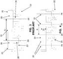
- the notch elements 20each comprise a front region 26 which is rectangular in shape, and a rearward or inner region 28 which is also rectangular in shape.
- the two regionsare centred on an axis 29 that is perpendicular to an edge 30 of the substrate 22 and it can be seen that the width of the front region 26 is greater than the dimension (or length) of the region in the direction normal to the edge of the substrate 22.
- the front region 26is formed contiguously with the rearward region 28, which is of smaller dimensions than the front region and has a width which is less than its length and which is less than the width of the front region 26.
- each element 20i.e. of the combined lengths of the front and rearward regions, is, as previously stated, less than 1/2 that of the Vivaldi element shown in Figure 2 . Nevertheless, the element can achieve bandwidths comparable to those available from the, much longer, Vivaldi element shown in Figures 1 and 2 .
- the upper frequency limit of the bandwidthdepends upon the spacing S between adjacent notch elements.
- the lower frequency limitdepends on the size of the notch elements. In a rectangular grid, the element can achieve up to one octave bandwidth.
- the scan angles availableare nominally a 60 degree half angle cone, although there are some frequencies and planes where the limit is closer to 50 degrees.
- the upper frequency limit of an elementis limited by the spacing between adjacent elements.
- a narrower spacingtherefore means an increase in the upper frequency limit.
- the metal between two elementsreduces in width.
- the present inventionprovides a radiating element and preferably an array antenna that seek to address the above limitations.
- the present inventionprovides an array of notch elements for an array antenna according to claim 1.
- the rearward regionis shaped as a polygon having an axis of symmetry normal to the edge of the substrate. Further, it is preferable that the rearward region has a dimension parallel to the edge smaller than its dimension normal to the edge.
- the axis of symmetry normal to the edge of the substratemay be the same for both front and rearward regions. Further preferably, the front and rearward regions are both substantially rectangular. It is preferable to provide a plurality of these notch elements on a substrate in a uniformly spaced arrangement.
- an electrically conductive striplineis provided for coupling the notch elements to a common source.
- the notch elementsare provided on only one surface of the substrate.
- the substratehas opposed major surfaces, a layer of conductive material being provided on each major surface, and an array of said notch elements being formed by the layer of conductive material on each major surface so that the notch elements on each major surface are in alignment and in correspondence with the other. It is preferable that the notch elements are aligned along an edge thereof in said uniformly spaced arrangement.
- notch elementsmay be provided having different shapes to that described below in the embodiments of the invention.
- An alternative arrangement of notch elementscan extend the frequency bandwidth of an antenna that includes such notch elements by removing conductive material altogether from between adjacent elements. This embodiment is shown in Figure 4 where, as can be seen, no gap is left between the front notch elements formed by the electrically conductive coating on the surface of the substrate.
- a plurality of notch elements 20 adjacent to one another in an array thereofare provided.
- Each element 20is formed by removing the coating from a substrate 22 coated with an electrically conductive material in a conventional manner.
- the elements formedare less than 1/2 the height of the comparable Vivaldi radiating element shown in Figure 1 (i.e. have a length of approximately one half wavelength at the centre frequency).
- the substrateis formed as a laminate with a stripline sandwiched between the layers of the laminate.
- the layers of the laminateare provided by two printed circuit boards arranged in a back-to-back relationship and the reverse side (not shown in Figure 4 ) of the laminate is substantially similar to the view shown in Figure 4 as the elements are aligned on the two external surfaces.
- the external surfaces of the laminated substrateare electrically coupled by vias 23 extending through the substrate. It should be noted that the arrangement of the vias 23 is an arbitrary choice by a skilled designer, so other options than that shown are available.
- the notch elements 20all comprise adjacent front regions 26, such that a continuous front region is formed, and a rearward, or inner, region 28. Both front and rearward, or inner, regions are rectangular in shape and are centred on an axis 29 that is perpendicular to an edge 30 of the substrate. It can be seen that the width of the front region 26 is greater than the dimension (or length) of the region in the direction normal to the edge of the substrate 22.
- the front region 26is formed contiguously with the adjacent front regions 26. Further, the front region 26 is formed contiguously with the rearward region 28, which is smaller dimensions that the front region 26 and has a width which is less than its length and which is less than the width of the front region 26.
- each element 20i.e. of the combined lengths of the front region 26 and rearward region 28, is, as previously stated, less than 1 ⁇ 2 that of the Vivaldi element shown in Figure 2 .
- the spacing between the elementsis minimised, allowing a higher upper frequency limit than that provided in the aforementioned embodiment while retaining the lower frequency limit of the aforementioned embodiment as the size of the elements remain the same. It has been calculated that any array of these elements, and therefore an array comprising those elements, can function over an extended bandwidth of approximate frequency f1 ⁇ frequency ⁇ 2.5 x f1 over a full 60 degree cone.
- the construction of the antennas of Figures 3 and 4is created on a laminated substrate, it is to be clearly understood that the invention can be implemented by providing a notch element array on single surface only of a substrate with the required stripline (normally called a microstrip in this case) formed on a reverse face of the substrate from that on which the elements are formed.
- a notch element arrayon single surface only of a substrate with the required stripline (normally called a microstrip in this case) formed on a reverse face of the substrate from that on which the elements are formed.
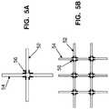
- FIG. 5Ais a diagrammatic illustration of notch element modules 52, 54 used in constructing a grid of modules as shown in Figure 5B .
- vertical modules 54 and horizontal modules 52are arranged in a grid pattern using metal posts 56 to secure the modules 52, 54 in place.
- the elements in such an array of elementsneeds to be less than ⁇ /2 in length in the direction of the axis of symmetry. This provides improved cross-polar performance in comparison with the performance of a similar array of Vivaldi elements or an array of notch elements.
Landscapes
- Variable-Direction Aerials And Aerial Arrays (AREA)
- Waveguide Aerials (AREA)
- Details Of Aerials (AREA)
Description
- This invention is concerned with antennas and is more specifically concerned with notch radiating elements used in antenna arrays.
- Radiating elements are small antennas that have a wide radiation pattern. They are used as the individual radiating elements in an electronically scanned array antenna (ESCAN). The elements are normally arranged on a rectangular or triangular grid with a transmit/receive module (TRM) behind each element. These TRMs contain phase shifters that enable the antenna main beam to be steered by choosing a set of amplitude and phase weightings that represent a particular beam angle.
- A class of such antennas that have become widely adopted are called Tapered Slot Antennas (TSA) or Vivaldi elements. One advantage of these TSA or Vivaldi elements is that they are readily manufactured by printing onto a commercial microwave printed circuit board. An array of these elements comprises two boards, each having tapered slots printed onto the outside surfaces. A transmission input line, known as a stripline, is located between the boards, on their inner surfaces, before the boards are bonded together. Such a known design is illustrated in
Figure 1 . It is also known to construct an array of these elements having just a single board with tapered slots printed on one side and a transmission input line bonded to the other side. - Vivaldi elements are now well known and a number of different designs thereof have been proposed to fulfil different requirements. It is important in designing these elements to ensure that almost all of the power that is fed into the element via the
stripline 11 is actually radiated into free space via thetapered slot 12 at the top of the element (seeFigure 1 ). One common problem is that the power input may be reflected back from thestripline input port 13 rather than being radiated. Furthermore, the mutual coupling between the elements in the array also contributes to this reflected power. It is important to ensure, when designing these elements, that the reflected power (reflection coefficient) is minimised over all scan angles and frequencies at which the array operates. Conventionally, a radiating element is designed to operate over a range of angles within a cone having a 60-degree semi angle. - Each of the
elements 10 shown inFigure 1 has a length L, measured in a direction normal to the edge of the substrate. Length L is typically 1 - 2 times the wavelength of the radiation that the element generates, in order to allow operation over wide bandwidths. The bandwidth achieved is typically greater than one octave when employed in free space. - The spacing between adjacent elements of an array antenna, a portion of which is shown in
Figure 2 , must be less than half a wavelength at the maximum operating frequency, in a rectangular grid, in order to prevent grating lobes (images of the main beam) occurring. This has the effect of limiting the lowest operating frequency, where the wavelength is longest, because the elements need to be wider where the wavelength is longest. However, this dimension is constrained because the spacing between adjacent elements must be less than half a wavelength at the top of the band to prevent the occurrence of grating lobes. - Further, to increase the upper frequency at which a Vivaldi element operates in an ESCAN array, it is necessary to reduce the physical separation between the elements from, for example, about 15 mm for a theoretical 10 GHz upper limit to about 7.5 mm for a theoretical 20 GHz upper limit. This has the effect of further limiting the lower frequency at which the elements can operate, because the slot of the element is not wide enough for wavelengths at the bottom end of the band.
- To address these problems there can be provided a simple notch element profile, as shown in
Figure 3 , which illustrates a pair of adjacent such elements in an array thereof. Eachelement 20 is formed by removing the coating from asubstrate 22 coated with an electrically conductive material in a conventional manner. The elements formed are less than 1/2 the height of the comparable Vivaldi radiating element shown inFigure 1 (i.e. have a length of approximately one half wavelength at the centre frequency). In this arrangement, it is to be understood that the substrate is formed as a laminate with a stripline sandwiched between the layers of the laminate. The layers of the laminate are provided by two printed circuit boards arranged in a back-to-back relationship and the reverse side (not shown inFigure 3 ) of the laminate is substantially similar to the view shown inFigure 3 as the elements are aligned on the two external surfaces. The external surfaces of the laminated substrate are electrically coupled byvias 23 extending through the substrate. It should be noted that the arrangement of thevias 23 is an arbitrary choice by a skilled designer, so other options than that shown are available. - Preferably, each element or array of elements are made using two boards, each board comprising a dielectric material having a copper layer coating both sides. For a first board, areas of the metal coating are removed from one surface to form the elements and from the other surface to form the stripline feed. For a second board, areas of the metal coating are similarly removed to form the elements and the other side has all of the metal coating removed. The two boards are bonded together so that the elements are provided on the outer facing surfaces and a stripline feed is provided in the middle, between the inner surfaces of the boards.
- As can be seen from
Figure 3 , thenotch elements 20 each comprise afront region 26 which is rectangular in shape, and a rearward orinner region 28 which is also rectangular in shape. The two regions are centred on anaxis 29 that is perpendicular to anedge 30 of thesubstrate 22 and it can be seen that the width of thefront region 26 is greater than the dimension (or length) of the region in the direction normal to the edge of thesubstrate 22. Thefront region 26 is formed contiguously with therearward region 28, which is of smaller dimensions than the front region and has a width which is less than its length and which is less than the width of thefront region 26. - The total length of each
element 20, i.e. of the combined lengths of the front and rearward regions, is, as previously stated, less than 1/2 that of the Vivaldi element shown inFigure 2 . Nevertheless, the element can achieve bandwidths comparable to those available from the, much longer, Vivaldi element shown inFigures 1 and 2 . The upper frequency limit of the bandwidth depends upon the spacing S between adjacent notch elements. The lower frequency limit depends on the size of the notch elements. In a rectangular grid, the element can achieve up to one octave bandwidth. The scan angles available are nominally a 60 degree half angle cone, although there are some frequencies and planes where the limit is closer to 50 degrees. - It was noted above that the upper frequency limit of an element is limited by the spacing between adjacent elements. A narrower spacing therefore means an increase in the upper frequency limit. However, as the grid spacing reduces, the metal between two elements reduces in width. Thus, an advantage of such an arrangement of elements is that it substantially maintains the lower frequency range, as the elements retain the same dimensions, but increases the higher frequency range as the spacing between the elements decreases, relative to a Vivaldi element.
- As such, the present invention provides a radiating element and preferably an array antenna that seek to address the above limitations.
US6239761 ,WO97/15094 US6317094 ,EP0831550 US5202698 , andWUNSCH G J ET AL, "FULL AND PARTIAL CROSSWALLS BETWEEN UNIT CELLS OF ENDFIRE SLOTLINE ARRAYS", IEEE TRANSACTIONS ON ANTENNAS AND PROPAGATION, IEEE SERVICE CENTER, PISCATAWAY, NJ, US, (200006), vol. 48, no. 6, ISSN 0018-926X, pages 981 - 986, describe other examples of notch element antenna array.- Accordingly, the present invention provides an array of notch elements for an array antenna according to claim 1.
- It is preferable that the rearward region is shaped as a polygon having an axis of symmetry normal to the edge of the substrate. Further, it is preferable that the rearward region has a dimension parallel to the edge smaller than its dimension normal to the edge.
- Preferably, the axis of symmetry normal to the edge of the substrate may be the same for both front and rearward regions. Further preferably, the front and rearward regions are both substantially rectangular. It is preferable to provide a plurality of these notch elements on a substrate in a uniformly spaced arrangement.
- Preferably, an electrically conductive stripline is provided for coupling the notch elements to a common source.
- It is also possible for the notch elements are provided on only one surface of the substrate. Preferably, the substrate has opposed major surfaces, a layer of conductive material being provided on each major surface, and an array of said notch elements being formed by the layer of conductive material on each major surface so that the notch elements on each major surface are in alignment and in correspondence with the other. It is preferable that the notch elements are aligned along an edge thereof in said uniformly spaced arrangement.
- It should be understood that the notch elements may be provided having different shapes to that described below in the embodiments of the invention.
- Specific embodiments of the invention will now be described, by way of example only, with reference to the accompanying drawings that have like reference numerals, wherein:-
Figure 1 is a diagrammatic illustration of a part of one surface of an array antenna illustrating a Tapered Slot Antenna (TSA) or Vivaldi elements, as known in the art;Figure 2 shows a view of an array antenna utilising the TSA or Vivaldi elements shown inFigure 1 , as known in the art;Figure 3 is a diagrammatic illustration of a part of one surface of a prior art array antenna illustrating two adjacent notch elements provided at an edge of a substrate of an array antenna;Figure 4 is a diagrammatic illustration of a part of one surface of an array antenna illustrating four adjacent notch elements provided at an edge of a substrate of an array antenna in accordance with one aspect of the present invention; andFigures 5A and 5B are diagrammatic views of arrangements of notch elements according to the present invention arranged in a 90 degree grid to provide dual polarised wide band operation.- An alternative arrangement of notch elements, according to a preferred embodiment of the present invention, can extend the frequency bandwidth of an antenna that includes such notch elements by removing conductive material altogether from between adjacent elements. This embodiment is shown in
Figure 4 where, as can be seen, no gap is left between the front notch elements formed by the electrically conductive coating on the surface of the substrate. - In this preferred embodiment, there is provided a plurality of
notch elements 20 adjacent to one another in an array thereof. Eachelement 20 is formed by removing the coating from asubstrate 22 coated with an electrically conductive material in a conventional manner. The elements formed are less than 1/2 the height of the comparable Vivaldi radiating element shown inFigure 1 (i.e. have a length of approximately one half wavelength at the centre frequency). In this embodiment, it is to be understood that the substrate is formed as a laminate with a stripline sandwiched between the layers of the laminate. The layers of the laminate are provided by two printed circuit boards arranged in a back-to-back relationship and the reverse side (not shown inFigure 4 ) of the laminate is substantially similar to the view shown inFigure 4 as the elements are aligned on the two external surfaces. The external surfaces of the laminated substrate are electrically coupled byvias 23 extending through the substrate. It should be noted that the arrangement of thevias 23 is an arbitrary choice by a skilled designer, so other options than that shown are available. - As can be seen from
Figure 4 , thenotch elements 20 all comprise adjacentfront regions 26, such that a continuous front region is formed, and a rearward, or inner,region 28. Both front and rearward, or inner, regions are rectangular in shape and are centred on anaxis 29 that is perpendicular to anedge 30 of the substrate. It can be seen that the width of thefront region 26 is greater than the dimension (or length) of the region in the direction normal to the edge of thesubstrate 22. Thefront region 26 is formed contiguously with the adjacentfront regions 26. Further, thefront region 26 is formed contiguously with therearward region 28, which is smaller dimensions that thefront region 26 and has a width which is less than its length and which is less than the width of thefront region 26. - The total length of each
element 20, i.e. of the combined lengths of thefront region 26 andrearward region 28, is, as previously stated, less than ½ that of the Vivaldi element shown inFigure 2 . As thefront regions 26 of theelements 20 are contiguous, the spacing between the elements is minimised, allowing a higher upper frequency limit than that provided in the aforementioned embodiment while retaining the lower frequency limit of the aforementioned embodiment as the size of the elements remain the same. It has been calculated that any array of these elements, and therefore an array comprising those elements, can function over an extended bandwidth of approximate frequency f1 < frequency < 2.5 x f1 over a full 60 degree cone. - Though the construction of the antennas of
Figures 3 and 4 is created on a laminated substrate, it is to be clearly understood that the invention can be implemented by providing a notch element array on single surface only of a substrate with the required stripline (normally called a microstrip in this case) formed on a reverse face of the substrate from that on which the elements are formed. - The result of extending the bandwidth with elements arranged in an array antenna as described is that, by placing the elements in a grid at 90 degrees between vertical and horizontal array planes, the elements can also provide dual polarised wide band operation, as shown in
Figures 5A and 5B whereFigure 5A is a diagrammatic illustration ofnotch element modules Figure 5B . Herevertical modules 54 andhorizontal modules 52 are arranged in a grid pattern usingmetal posts 56 to secure themodules - In order to obtain good cross-polarisation at all scan angles, the elements in such an array of elements needs to be less than λ/2 in length in the direction of the axis of symmetry. This provides improved cross-polar performance in comparison with the performance of a similar array of Vivaldi elements or an array of notch elements.
Claims (9)
- An array of notch elements (20) on a substrate for an array antenna, each notch element (20) of the array being formed on the substrate, each notch element comprising a first region (26) and a second region (28), wherein the first region (26) is adjacent to an edge (30) of the substrate and is shaped as a symmetrical polygon having an axis (29) of symmetry normal to the edge (30) of the substrate, and wherein the first regions of notch elements (20) that are situated directly adjacent to one another being contiguous to provide a continuous first region adjacent the edge (30) of the substrate;characterised in that the first region has a dimension parallel to the edge which is greater than its dimension normal to the edge.
- An array of notch elements according to any preceding claim, wherein the second region is shaped as a polygon having an axis of symmetry normal to the edge of the substrate.
- An array of notch elements according to any preceding claim, the second region having a dimension parallel to the edge and a dimension normal to the edge, wherein the dimension parallel to the edge is smaller than the dimension normal to the edge.
- An array of notch elements according to any of claims 2 or 3, wherein the axis of symmetry normal to the edge of the substrate is the same for both first and second regions.
- An array of notch elements according to any preceding claim, wherein the first and second regions are both substantially rectangular.
- An array of notch elements according to claim 1, wherein the notch elements are provided on only one surface of the substrate.
- An array of notch elements according to any claim 1 to 6, wherein an electrically conductive microstrip is provided for coupling the notch elements to a common source.
- An array of notch elements according to any claim1 to 7, wherein the substrate has opposed major surfaces, a layer of conductive material being provided on each major surface, and an array of said notch elements being formed by the layer of conductive material on each major surface so that the notch elements on each major surface are in alignment with the other.
- An antenna comprising the array of notch elements of any one of claims 1-8 wherein the notch elements are aligned along an edge of the antenna in said uniformly spaced arrangement.
Applications Claiming Priority (4)
| Application Number | Priority Date | Filing Date | Title |
|---|---|---|---|
| GB0523818AGB0523818D0 (en) | 2005-11-23 | 2005-11-23 | Antennas |
| EP05257197 | 2005-11-23 | ||
| EP06808751AEP1952482A2 (en) | 2005-11-23 | 2006-11-14 | Antennas |
| PCT/GB2006/050387WO2007060477A2 (en) | 2005-11-23 | 2006-11-14 | Notch antenna element and array |
Related Parent Applications (1)
| Application Number | Title | Priority Date | Filing Date |
|---|---|---|---|
| EP06808751ADivisionEP1952482A2 (en) | 2005-11-23 | 2006-11-14 | Antennas |
Publications (2)
| Publication Number | Publication Date |
|---|---|
| EP3528340A1 EP3528340A1 (en) | 2019-08-21 |
| EP3528340B1true EP3528340B1 (en) | 2020-12-30 |
Family
ID=37613889
Family Applications (2)
| Application Number | Title | Priority Date | Filing Date |
|---|---|---|---|
| EP06808751ACeasedEP1952482A2 (en) | 2005-11-23 | 2006-11-14 | Antennas |
| EP19163850.1AActiveEP3528340B1 (en) | 2005-11-23 | 2006-11-14 | Antennas |
Family Applications Before (1)
| Application Number | Title | Priority Date | Filing Date |
|---|---|---|---|
| EP06808751ACeasedEP1952482A2 (en) | 2005-11-23 | 2006-11-14 | Antennas |
Country Status (6)
| Country | Link |
|---|---|
| US (1) | US7683847B2 (en) |
| EP (2) | EP1952482A2 (en) |
| JP (2) | JP2009516975A (en) |
| AU (1) | AU2006318825B2 (en) |
| ES (1) | ES2866550T3 (en) |
| WO (1) | WO2007060477A2 (en) |
Families Citing this family (3)
| Publication number | Priority date | Publication date | Assignee | Title |
|---|---|---|---|---|
| FR2909486A1 (en)* | 2006-12-01 | 2008-06-06 | Thomson Licensing Sas | MULTI-SECTOR ANTENNA |
| KR101895888B1 (en)* | 2016-11-29 | 2018-09-07 | 엘아이케이테크(주) | Filter and radio frequency package having microstrip line |
| CN108134191B (en)* | 2017-12-08 | 2020-01-24 | 中国船舶重工集团公司第七二四研究所 | Polarization component selectable ultra-wideband antenna array based on cross structure |
Citations (1)
| Publication number | Priority date | Publication date | Assignee | Title |
|---|---|---|---|---|
| US6239761B1 (en)* | 1996-08-29 | 2001-05-29 | Trw Inc. | Extended dielectric material tapered slot antenna |
Family Cites Families (20)
| Publication number | Priority date | Publication date | Assignee | Title |
|---|---|---|---|---|
| US3836976A (en) | 1973-04-19 | 1974-09-17 | Raytheon Co | Closely spaced orthogonal dipole array |
| GB2220303A (en) | 1988-06-29 | 1990-01-04 | Philips Electronic Associated | Dual polarised phased array antenna |
| US5023623A (en)* | 1989-12-21 | 1991-06-11 | Hughes Aircraft Company | Dual mode antenna apparatus having slotted waveguide and broadband arrays |
| FR2667198B1 (en)* | 1990-09-21 | 1993-08-13 | Applic Rech Electro Ste | DIRECTIVE NETWORK FOR RADIOCOMMUNICATIONS, WITH ADJACENT RADIANT ELEMENTS AND SET OF SUCH DIRECTIVE NETWORKS. |
| US5187489A (en)* | 1991-08-26 | 1993-02-16 | Hughes Aircraft Company | Asymmetrically flared notch radiator |
| US5268701A (en) | 1992-03-23 | 1993-12-07 | Raytheon Company | Radio frequency antenna |
| US5309165A (en)* | 1992-05-09 | 1994-05-03 | Westinghouse Electric Corp. | Positioner with corner contacts for cross notch array and improved radiator elements |
| US5786792A (en)* | 1994-06-13 | 1998-07-28 | Northrop Grumman Corporation | Antenna array panel structure |
| JP3286882B2 (en)* | 1995-06-22 | 2002-05-27 | 三菱電機株式会社 | Antenna device |
| AU6142396A (en) | 1995-10-19 | 1997-05-07 | Boris Iosifovich Sukhovetsky | Wideband antenna array |
| FR2753568B1 (en) | 1996-09-19 | 1998-11-13 | Dassault Electronique | VERSATILE NETWORK ANTENNA |
| US6317094B1 (en)* | 1999-05-24 | 2001-11-13 | Litva Antenna Enterprises Inc. | Feed structures for tapered slot antennas |
| JP3433222B2 (en) | 2000-05-10 | 2003-08-04 | 防衛庁技術研究本部長 | Antenna device |
| US6525696B2 (en)* | 2000-12-20 | 2003-02-25 | Radio Frequency Systems, Inc. | Dual band antenna using a single column of elliptical vivaldi notches |
| US6778145B2 (en) | 2002-07-03 | 2004-08-17 | Northrop Grumman Corporation | Wideband antenna with tapered surfaces |
| US6850204B1 (en) | 2002-11-07 | 2005-02-01 | Lockheed Martin Corporation | Clip for radar array, and array including the clip |
| JP2004253850A (en)* | 2003-02-18 | 2004-09-09 | Toyota Central Res & Dev Lab Inc | Antenna device and vehicle equipped with antenna device |
| JP4378096B2 (en)* | 2003-03-18 | 2009-12-02 | 友訊科技股▲分▼有限公司 | Printed dual-band trumpet antenna structure |
| JP2005167830A (en)* | 2003-12-04 | 2005-06-23 | Alps Electric Co Ltd | Slot antenna |
| US7138952B2 (en)* | 2005-01-11 | 2006-11-21 | Raytheon Company | Array antenna with dual polarization and method |
- 2006
- 2006-11-14WOPCT/GB2006/050387patent/WO2007060477A2/enactiveApplication Filing
- 2006-11-14EPEP06808751Apatent/EP1952482A2/ennot_activeCeased
- 2006-11-14ESES19163850Tpatent/ES2866550T3/enactiveActive
- 2006-11-14JPJP2008541832Apatent/JP2009516975A/ennot_activeWithdrawn
- 2006-11-14USUS11/659,546patent/US7683847B2/enactiveActive
- 2006-11-14AUAU2006318825Apatent/AU2006318825B2/enactiveActive
- 2006-11-14EPEP19163850.1Apatent/EP3528340B1/enactiveActive
- 2013
- 2013-05-08JPJP2013098631Apatent/JP5657742B2/enactiveActive
Patent Citations (1)
| Publication number | Priority date | Publication date | Assignee | Title |
|---|---|---|---|---|
| US6239761B1 (en)* | 1996-08-29 | 2001-05-29 | Trw Inc. | Extended dielectric material tapered slot antenna |
Also Published As
| Publication number | Publication date |
|---|---|
| AU2006318825B2 (en) | 2011-03-17 |
| EP1952482A2 (en) | 2008-08-06 |
| US20090102734A1 (en) | 2009-04-23 |
| ES2866550T3 (en) | 2021-10-19 |
| JP2013211869A (en) | 2013-10-10 |
| JP5657742B2 (en) | 2015-01-21 |
| EP3528340A1 (en) | 2019-08-21 |
| JP2009516975A (en) | 2009-04-23 |
| WO2007060477A3 (en) | 2007-08-02 |
| US7683847B2 (en) | 2010-03-23 |
| AU2006318825A1 (en) | 2007-05-31 |
| WO2007060477A2 (en) | 2007-05-31 |
Similar Documents
| Publication | Publication Date | Title |
|---|---|---|
| US11196184B2 (en) | Broadband antenna array | |
| US8830133B2 (en) | Circularly polarised array antenna | |
| EP0456680B1 (en) | Antenna arrays | |
| US7898480B2 (en) | Antenna | |
| US7109939B2 (en) | Wideband antenna array | |
| JP5983760B2 (en) | Array antenna | |
| US7026993B2 (en) | Planar antenna and array antenna | |
| US7061443B2 (en) | MMW electronically scanned antenna | |
| US6919854B2 (en) | Variable inclination continuous transverse stub array | |
| JP4506728B2 (en) | Antenna device and radar | |
| US20080238793A1 (en) | Compact Planar Antenna For Single and Multiple Polarization Configurations | |
| US20060044189A1 (en) | Radome structure | |
| CN105244609A (en) | Broadband vivaldi array antenna bases on cross feed pedestal | |
| GB1573481A (en) | Radio frequency multibeam antenna | |
| CA2570652A1 (en) | Dual polarization antenna array with inter-element capacitive coupling plate and associated methods | |
| EP3528340B1 (en) | Antennas | |
| US6703980B2 (en) | Active dual-polarization microwave reflector, in particular for electronically scanning antenna | |
| US10950952B1 (en) | Spherical space feed for antenna array systems and methods | |
| JP7591401B2 (en) | Array Antenna | |
| CA2046301C (en) | Antenna arrays | |
| CN119181963A (en) | Patch antenna, omni-directional antenna array and coplanar radiating antenna array comprising same |
Legal Events
| Date | Code | Title | Description |
|---|---|---|---|
| PUAI | Public reference made under article 153(3) epc to a published international application that has entered the european phase | Free format text:ORIGINAL CODE: 0009012 | |
| STAA | Information on the status of an ep patent application or granted ep patent | Free format text:STATUS: THE APPLICATION HAS BEEN PUBLISHED | |
| AC | Divisional application: reference to earlier application | Ref document number:1952482 Country of ref document:EP Kind code of ref document:P | |
| AK | Designated contracting states | Kind code of ref document:A1 Designated state(s):AT BE BG CH CY CZ DE DK EE ES FI FR GB GR HU IE IS IT LI LT LU LV MC NL PL PT RO SE SI SK TR | |
| STAA | Information on the status of an ep patent application or granted ep patent | Free format text:STATUS: REQUEST FOR EXAMINATION WAS MADE | |
| 17P | Request for examination filed | Effective date:20191112 | |
| RBV | Designated contracting states (corrected) | Designated state(s):AT BE BG CH CY CZ DE DK EE ES FI FR GB GR HU IE IS IT LI LT LU LV MC NL PL PT RO SE SI SK TR | |
| STAA | Information on the status of an ep patent application or granted ep patent | Free format text:STATUS: EXAMINATION IS IN PROGRESS | |
| 17Q | First examination report despatched | Effective date:20200730 | |
| GRAP | Despatch of communication of intention to grant a patent | Free format text:ORIGINAL CODE: EPIDOSNIGR1 | |
| STAA | Information on the status of an ep patent application or granted ep patent | Free format text:STATUS: GRANT OF PATENT IS INTENDED | |
| GRAS | Grant fee paid | Free format text:ORIGINAL CODE: EPIDOSNIGR3 | |
| INTG | Intention to grant announced | Effective date:20200923 | |
| GRAA | (expected) grant | Free format text:ORIGINAL CODE: 0009210 | |
| STAA | Information on the status of an ep patent application or granted ep patent | Free format text:STATUS: THE PATENT HAS BEEN GRANTED | |
| AC | Divisional application: reference to earlier application | Ref document number:1952482 Country of ref document:EP Kind code of ref document:P | |
| AK | Designated contracting states | Kind code of ref document:B1 Designated state(s):AT BE BG CH CY CZ DE DK EE ES FI FR GB GR HU IE IS IT LI LT LU LV MC NL PL PT RO SE SI SK TR | |
| REG | Reference to a national code | Ref country code:GB Ref legal event code:FG4D | |
| REG | Reference to a national code | Ref country code:DE Ref legal event code:R096 Ref document number:602006059874 Country of ref document:DE | |
| REG | Reference to a national code | Ref country code:AT Ref legal event code:REF Ref document number:1350862 Country of ref document:AT Kind code of ref document:T Effective date:20210115 | |
| REG | Reference to a national code | Ref country code:IE Ref legal event code:FG4D | |
| REG | Reference to a national code | Ref country code:CH Ref legal event code:NV Representative=s name:INTELLECTUAL PROPERTY SERVICES GMBH, CH | |
| REG | Reference to a national code | Ref country code:FI Ref legal event code:FGE | |
| REG | Reference to a national code | Ref country code:SE Ref legal event code:TRGR | |
| PG25 | Lapsed in a contracting state [announced via postgrant information from national office to epo] | Ref country code:GR Free format text:LAPSE BECAUSE OF FAILURE TO SUBMIT A TRANSLATION OF THE DESCRIPTION OR TO PAY THE FEE WITHIN THE PRESCRIBED TIME-LIMIT Effective date:20210331 | |
| REG | Reference to a national code | Ref country code:CH Ref legal event code:PFA Owner name:LEONARDO UK LTD, GB Free format text:FORMER OWNER: LEONARDO MW LIMITED, GB | |
| RAP4 | Party data changed (patent owner data changed or rights of a patent transferred) | Owner name:LEONARDO UK LTD | |
| REG | Reference to a national code | Ref country code:AT Ref legal event code:MK05 Ref document number:1350862 Country of ref document:AT Kind code of ref document:T Effective date:20201230 | |
| PG25 | Lapsed in a contracting state [announced via postgrant information from national office to epo] | Ref country code:BG Free format text:LAPSE BECAUSE OF FAILURE TO SUBMIT A TRANSLATION OF THE DESCRIPTION OR TO PAY THE FEE WITHIN THE PRESCRIBED TIME-LIMIT Effective date:20210330 Ref country code:LV Free format text:LAPSE BECAUSE OF FAILURE TO SUBMIT A TRANSLATION OF THE DESCRIPTION OR TO PAY THE FEE WITHIN THE PRESCRIBED TIME-LIMIT Effective date:20201230 | |
| REG | Reference to a national code | Ref country code:NL Ref legal event code:MP Effective date:20201230 | |
| REG | Reference to a national code | Ref country code:LT Ref legal event code:MG9D | |
| REG | Reference to a national code | Ref country code:DE Ref legal event code:R082 Ref document number:602006059874 Country of ref document:DE Representative=s name:MANITZ FINSTERWALD PATENT- UND RECHTSANWALTSPA, DE Ref country code:DE Ref legal event code:R081 Ref document number:602006059874 Country of ref document:DE Owner name:LEONARDO UK LTD, GB Free format text:FORMER OWNER: LEONARDO MW LTD., BASILDON, ESSEX, GB | |
| PG25 | Lapsed in a contracting state [announced via postgrant information from national office to epo] | Ref country code:LT Free format text:LAPSE BECAUSE OF FAILURE TO SUBMIT A TRANSLATION OF THE DESCRIPTION OR TO PAY THE FEE WITHIN THE PRESCRIBED TIME-LIMIT Effective date:20201230 Ref country code:PT Free format text:LAPSE BECAUSE OF FAILURE TO SUBMIT A TRANSLATION OF THE DESCRIPTION OR TO PAY THE FEE WITHIN THE PRESCRIBED TIME-LIMIT Effective date:20210430 Ref country code:RO Free format text:LAPSE BECAUSE OF FAILURE TO SUBMIT A TRANSLATION OF THE DESCRIPTION OR TO PAY THE FEE WITHIN THE PRESCRIBED TIME-LIMIT Effective date:20201230 Ref country code:SK Free format text:LAPSE BECAUSE OF FAILURE TO SUBMIT A TRANSLATION OF THE DESCRIPTION OR TO PAY THE FEE WITHIN THE PRESCRIBED TIME-LIMIT Effective date:20201230 Ref country code:EE Free format text:LAPSE BECAUSE OF FAILURE TO SUBMIT A TRANSLATION OF THE DESCRIPTION OR TO PAY THE FEE WITHIN THE PRESCRIBED TIME-LIMIT Effective date:20201230 Ref country code:CZ Free format text:LAPSE BECAUSE OF FAILURE TO SUBMIT A TRANSLATION OF THE DESCRIPTION OR TO PAY THE FEE WITHIN THE PRESCRIBED TIME-LIMIT Effective date:20201230 | |
| PG25 | Lapsed in a contracting state [announced via postgrant information from national office to epo] | Ref country code:AT Free format text:LAPSE BECAUSE OF FAILURE TO SUBMIT A TRANSLATION OF THE DESCRIPTION OR TO PAY THE FEE WITHIN THE PRESCRIBED TIME-LIMIT Effective date:20201230 Ref country code:PL Free format text:LAPSE BECAUSE OF FAILURE TO SUBMIT A TRANSLATION OF THE DESCRIPTION OR TO PAY THE FEE WITHIN THE PRESCRIBED TIME-LIMIT Effective date:20201230 | |
| PG25 | Lapsed in a contracting state [announced via postgrant information from national office to epo] | Ref country code:IS Free format text:LAPSE BECAUSE OF FAILURE TO SUBMIT A TRANSLATION OF THE DESCRIPTION OR TO PAY THE FEE WITHIN THE PRESCRIBED TIME-LIMIT Effective date:20210430 | |
| REG | Reference to a national code | Ref country code:DE Ref legal event code:R097 Ref document number:602006059874 Country of ref document:DE | |
| REG | Reference to a national code | Ref country code:ES Ref legal event code:FG2A Ref document number:2866550 Country of ref document:ES Kind code of ref document:T3 Effective date:20211019 | |
| PLBE | No opposition filed within time limit | Free format text:ORIGINAL CODE: 0009261 | |
| STAA | Information on the status of an ep patent application or granted ep patent | Free format text:STATUS: NO OPPOSITION FILED WITHIN TIME LIMIT | |
| PG25 | Lapsed in a contracting state [announced via postgrant information from national office to epo] | Ref country code:DK Free format text:LAPSE BECAUSE OF FAILURE TO SUBMIT A TRANSLATION OF THE DESCRIPTION OR TO PAY THE FEE WITHIN THE PRESCRIBED TIME-LIMIT Effective date:20201230 | |
| 26N | No opposition filed | Effective date:20211001 | |
| PG25 | Lapsed in a contracting state [announced via postgrant information from national office to epo] | Ref country code:SI Free format text:LAPSE BECAUSE OF FAILURE TO SUBMIT A TRANSLATION OF THE DESCRIPTION OR TO PAY THE FEE WITHIN THE PRESCRIBED TIME-LIMIT Effective date:20201230 | |
| PG25 | Lapsed in a contracting state [announced via postgrant information from national office to epo] | Ref country code:IS Free format text:LAPSE BECAUSE OF FAILURE TO SUBMIT A TRANSLATION OF THE DESCRIPTION OR TO PAY THE FEE WITHIN THE PRESCRIBED TIME-LIMIT Effective date:20210430 | |
| PG25 | Lapsed in a contracting state [announced via postgrant information from national office to epo] | Ref country code:MC Free format text:LAPSE BECAUSE OF FAILURE TO SUBMIT A TRANSLATION OF THE DESCRIPTION OR TO PAY THE FEE WITHIN THE PRESCRIBED TIME-LIMIT Effective date:20201230 | |
| PG25 | Lapsed in a contracting state [announced via postgrant information from national office to epo] | Ref country code:LU Free format text:LAPSE BECAUSE OF NON-PAYMENT OF DUE FEES Effective date:20211114 Ref country code:BE Free format text:LAPSE BECAUSE OF NON-PAYMENT OF DUE FEES Effective date:20211130 | |
| REG | Reference to a national code | Ref country code:BE Ref legal event code:MM Effective date:20211130 | |
| PG25 | Lapsed in a contracting state [announced via postgrant information from national office to epo] | Ref country code:IE Free format text:LAPSE BECAUSE OF NON-PAYMENT OF DUE FEES Effective date:20211114 | |
| PG25 | Lapsed in a contracting state [announced via postgrant information from national office to epo] | Ref country code:CY Free format text:LAPSE BECAUSE OF FAILURE TO SUBMIT A TRANSLATION OF THE DESCRIPTION OR TO PAY THE FEE WITHIN THE PRESCRIBED TIME-LIMIT Effective date:20201230 | |
| PG25 | Lapsed in a contracting state [announced via postgrant information from national office to epo] | Ref country code:NL Free format text:LAPSE BECAUSE OF NON-PAYMENT OF DUE FEES Effective date:20201230 | |
| PG25 | Lapsed in a contracting state [announced via postgrant information from national office to epo] | Ref country code:HU Free format text:LAPSE BECAUSE OF FAILURE TO SUBMIT A TRANSLATION OF THE DESCRIPTION OR TO PAY THE FEE WITHIN THE PRESCRIBED TIME-LIMIT; INVALID AB INITIO Effective date:20061114 | |
| PGFP | Annual fee paid to national office [announced via postgrant information from national office to epo] | Ref country code:DE Payment date:20241121 Year of fee payment:19 | |
| PGFP | Annual fee paid to national office [announced via postgrant information from national office to epo] | Ref country code:FI Payment date:20241122 Year of fee payment:19 | |
| PGFP | Annual fee paid to national office [announced via postgrant information from national office to epo] | Ref country code:GB Payment date:20241120 Year of fee payment:19 | |
| PGFP | Annual fee paid to national office [announced via postgrant information from national office to epo] | Ref country code:FR Payment date:20241128 Year of fee payment:19 | |
| PGFP | Annual fee paid to national office [announced via postgrant information from national office to epo] | Ref country code:IT Payment date:20241120 Year of fee payment:19 Ref country code:ES Payment date:20241230 Year of fee payment:19 | |
| PGFP | Annual fee paid to national office [announced via postgrant information from national office to epo] | Ref country code:SE Payment date:20241120 Year of fee payment:19 | |
| PGFP | Annual fee paid to national office [announced via postgrant information from national office to epo] | Ref country code:CH Payment date:20241201 Year of fee payment:19 | |
| PGFP | Annual fee paid to national office [announced via postgrant information from national office to epo] | Ref country code:TR Payment date:20241104 Year of fee payment:19 |