EP3528295A1 - Display comprising led chip and method of manufacturing the same - Google Patents
Display comprising led chip and method of manufacturing the sameDownload PDFInfo
- Publication number
- EP3528295A1 EP3528295A1EP19169273.0AEP19169273AEP3528295A1EP 3528295 A1EP3528295 A1EP 3528295A1EP 19169273 AEP19169273 AEP 19169273AEP 3528295 A1EP3528295 A1EP 3528295A1
- Authority
- EP
- European Patent Office
- Prior art keywords
- leds
- led
- array
- substrate
- chips
- Prior art date
- Legal status (The legal status is an assumption and is not a legal conclusion. Google has not performed a legal analysis and makes no representation as to the accuracy of the status listed.)
- Granted
Links
Images


Classifications
- H—ELECTRICITY
- H10—SEMICONDUCTOR DEVICES; ELECTRIC SOLID-STATE DEVICES NOT OTHERWISE PROVIDED FOR
- H10H—INORGANIC LIGHT-EMITTING SEMICONDUCTOR DEVICES HAVING POTENTIAL BARRIERS
- H10H29/00—Integrated devices, or assemblies of multiple devices, comprising at least one light-emitting semiconductor element covered by group H10H20/00
- H10H29/10—Integrated devices comprising at least one light-emitting semiconductor component covered by group H10H20/00
- H10H29/14—Integrated devices comprising at least one light-emitting semiconductor component covered by group H10H20/00 comprising multiple light-emitting semiconductor components
- H10H29/142—Two-dimensional arrangements, e.g. asymmetric LED layout
- B—PERFORMING OPERATIONS; TRANSPORTING
- B41—PRINTING; LINING MACHINES; TYPEWRITERS; STAMPS
- B41J—TYPEWRITERS; SELECTIVE PRINTING MECHANISMS, i.e. MECHANISMS PRINTING OTHERWISE THAN FROM A FORME; CORRECTION OF TYPOGRAPHICAL ERRORS
- B41J2/00—Typewriters or selective printing mechanisms characterised by the printing or marking process for which they are designed
- B41J2/435—Typewriters or selective printing mechanisms characterised by the printing or marking process for which they are designed characterised by selective application of radiation to a printing material or impression-transfer material
- B41J2/447—Typewriters or selective printing mechanisms characterised by the printing or marking process for which they are designed characterised by selective application of radiation to a printing material or impression-transfer material using arrays of radiation sources
- B41J2/45—Typewriters or selective printing mechanisms characterised by the printing or marking process for which they are designed characterised by selective application of radiation to a printing material or impression-transfer material using arrays of radiation sources using light-emitting diode [LED] or laser arrays
- H—ELECTRICITY
- H01—ELECTRIC ELEMENTS
- H01L—SEMICONDUCTOR DEVICES NOT COVERED BY CLASS H10
- H01L25/00—Assemblies consisting of a plurality of semiconductor or other solid state devices
- H01L25/03—Assemblies consisting of a plurality of semiconductor or other solid state devices all the devices being of a type provided for in a single subclass of subclasses H10B, H10D, H10F, H10H, H10K or H10N, e.g. assemblies of rectifier diodes
- H01L25/04—Assemblies consisting of a plurality of semiconductor or other solid state devices all the devices being of a type provided for in a single subclass of subclasses H10B, H10D, H10F, H10H, H10K or H10N, e.g. assemblies of rectifier diodes the devices not having separate containers
- H01L25/075—Assemblies consisting of a plurality of semiconductor or other solid state devices all the devices being of a type provided for in a single subclass of subclasses H10B, H10D, H10F, H10H, H10K or H10N, e.g. assemblies of rectifier diodes the devices not having separate containers the devices being of a type provided for in group H10H20/00
- H01L25/0753—Assemblies consisting of a plurality of semiconductor or other solid state devices all the devices being of a type provided for in a single subclass of subclasses H10B, H10D, H10F, H10H, H10K or H10N, e.g. assemblies of rectifier diodes the devices not having separate containers the devices being of a type provided for in group H10H20/00 the devices being arranged next to each other
- H—ELECTRICITY
- H01—ELECTRIC ELEMENTS
- H01L—SEMICONDUCTOR DEVICES NOT COVERED BY CLASS H10
- H01L25/00—Assemblies consisting of a plurality of semiconductor or other solid state devices
- H01L25/50—Multistep manufacturing processes of assemblies consisting of devices, the devices being individual devices of subclass H10D or integrated devices of class H10
- H—ELECTRICITY
- H10—SEMICONDUCTOR DEVICES; ELECTRIC SOLID-STATE DEVICES NOT OTHERWISE PROVIDED FOR
- H10H—INORGANIC LIGHT-EMITTING SEMICONDUCTOR DEVICES HAVING POTENTIAL BARRIERS
- H10H20/00—Individual inorganic light-emitting semiconductor devices having potential barriers, e.g. light-emitting diodes [LED]
- H10H20/80—Constructional details
- H10H20/81—Bodies
- H10H20/819—Bodies characterised by their shape, e.g. curved or truncated substrates
- H—ELECTRICITY
- H10—SEMICONDUCTOR DEVICES; ELECTRIC SOLID-STATE DEVICES NOT OTHERWISE PROVIDED FOR
- H10H—INORGANIC LIGHT-EMITTING SEMICONDUCTOR DEVICES HAVING POTENTIAL BARRIERS
- H10H20/00—Individual inorganic light-emitting semiconductor devices having potential barriers, e.g. light-emitting diodes [LED]
- H10H20/80—Constructional details
- H10H20/85—Packages
- H10H20/857—Interconnections, e.g. lead-frames, bond wires or solder balls
- H—ELECTRICITY
- H10—SEMICONDUCTOR DEVICES; ELECTRIC SOLID-STATE DEVICES NOT OTHERWISE PROVIDED FOR
- H10H—INORGANIC LIGHT-EMITTING SEMICONDUCTOR DEVICES HAVING POTENTIAL BARRIERS
- H10H29/00—Integrated devices, or assemblies of multiple devices, comprising at least one light-emitting semiconductor element covered by group H10H20/00
- H10H29/10—Integrated devices comprising at least one light-emitting semiconductor component covered by group H10H20/00
- H10H29/14—Integrated devices comprising at least one light-emitting semiconductor component covered by group H10H20/00 comprising multiple light-emitting semiconductor components
- H—ELECTRICITY
- H10—SEMICONDUCTOR DEVICES; ELECTRIC SOLID-STATE DEVICES NOT OTHERWISE PROVIDED FOR
- H10K—ORGANIC ELECTRIC SOLID-STATE DEVICES
- H10K59/00—Integrated devices, or assemblies of multiple devices, comprising at least one organic light-emitting element covered by group H10K50/00
- H10K59/10—OLED displays
- H10K59/12—Active-matrix OLED [AMOLED] displays
- H10K59/121—Active-matrix OLED [AMOLED] displays characterised by the geometry or disposition of pixel elements
- H10K59/1216—Active-matrix OLED [AMOLED] displays characterised by the geometry or disposition of pixel elements the pixel elements being capacitors
- H—ELECTRICITY
- H10—SEMICONDUCTOR DEVICES; ELECTRIC SOLID-STATE DEVICES NOT OTHERWISE PROVIDED FOR
- H10K—ORGANIC ELECTRIC SOLID-STATE DEVICES
- H10K59/00—Integrated devices, or assemblies of multiple devices, comprising at least one organic light-emitting element covered by group H10K50/00
- H10K59/80—Constructional details
- H10K59/84—Parallel electrical configurations of multiple OLEDs
- H—ELECTRICITY
- H10—SEMICONDUCTOR DEVICES; ELECTRIC SOLID-STATE DEVICES NOT OTHERWISE PROVIDED FOR
- H10K—ORGANIC ELECTRIC SOLID-STATE DEVICES
- H10K59/00—Integrated devices, or assemblies of multiple devices, comprising at least one organic light-emitting element covered by group H10K50/00
- H10K59/80—Constructional details
- H10K59/86—Series electrical configurations of multiple OLEDs
- B—PERFORMING OPERATIONS; TRANSPORTING
- B41—PRINTING; LINING MACHINES; TYPEWRITERS; STAMPS
- B41J—TYPEWRITERS; SELECTIVE PRINTING MECHANISMS, i.e. MECHANISMS PRINTING OTHERWISE THAN FROM A FORME; CORRECTION OF TYPOGRAPHICAL ERRORS
- B41J2202/00—Embodiments of or processes related to ink-jet or thermal heads
- B41J2202/50—Embodiments of processes related to optical heads
- H—ELECTRICITY
- H01—ELECTRIC ELEMENTS
- H01L—SEMICONDUCTOR DEVICES NOT COVERED BY CLASS H10
- H01L2924/00—Indexing scheme for arrangements or methods for connecting or disconnecting semiconductor or solid-state bodies as covered by H01L24/00
- H01L2924/0001—Technical content checked by a classifier
- H01L2924/0002—Not covered by any one of groups H01L24/00, H01L24/00 and H01L2224/00
- H—ELECTRICITY
- H01—ELECTRIC ELEMENTS
- H01L—SEMICONDUCTOR DEVICES NOT COVERED BY CLASS H10
- H01L2924/00—Indexing scheme for arrangements or methods for connecting or disconnecting semiconductor or solid-state bodies as covered by H01L24/00
- H01L2924/10—Details of semiconductor or other solid state devices to be connected
- H01L2924/11—Device type
- H01L2924/12—Passive devices, e.g. 2 terminal devices
- H01L2924/1204—Optical Diode
- H01L2924/12041—LED
- H—ELECTRICITY
- H10—SEMICONDUCTOR DEVICES; ELECTRIC SOLID-STATE DEVICES NOT OTHERWISE PROVIDED FOR
- H10H—INORGANIC LIGHT-EMITTING SEMICONDUCTOR DEVICES HAVING POTENTIAL BARRIERS
- H10H20/00—Individual inorganic light-emitting semiconductor devices having potential barriers, e.g. light-emitting diodes [LED]
- H10H20/01—Manufacture or treatment
- H10H20/036—Manufacture or treatment of packages
Definitions
- the inventionrelates to a display, comprising a light emitting diode (LED) chip and a method of manufacturing a display comprising forming of an LED chip. More specifically, the invention relates to, but is not limited to, LED chips and methods of manufacturing LED chips that may be placed adjacent one another to form continuous arrays of LEDs.
- LEDlight emitting diode
- LEDsare a form of semiconductor material that convert electrical energy into optical energy.
- lightis typically generated through recombination of electrons, originating from an n-type doped semiconductor layer, and holes originating from a p-type doped semiconductor layer.
- lightcan be generated by electron intersub-band transitions rather than electron hole transitions.
- a major challenge in the fieldis to extract as much of the emitted light as possible from the semiconductor material into the surrounding medium, usually air. This is hindered by total internal reflection at the surfaces of the semiconductor.
- the average path length for light rays within the semiconductoris long, and the average number of reflections of an emitted light ray at semiconductor surfaces is high, prior to escape. Long path lengths and reflections at metal coated semiconductor surfaces may lead to absorption losses.
- a further approach to achieving high extraction efficiency (EE) and maximum useable light from a chipis to provide an array of "micro-LEDs” ( ⁇ LEDs), as such devices keep the average path length within the device short. Arrangements are described in US 6,410,940 and US 6,410,942 .
- US 7,518, 149describes a ⁇ LED that is an integrated diode structure in a mesa, in which the mesa shape and the light-emitting region are chosen for efficiency.
- a ⁇ LEDmay include, on a substrate and a semiconductor layer, a mesa, a light emitting layer, and an electrical contact.
- the ⁇ LEDs in this devicemay have improved EE because of their shape. Light is generated within the mesa, which is shaped to enhance the escape probability of the light.
- improved EEsmay be achieved with a near parabolic mesa that has a high aspect ratio.
- the top of the mesais truncated above the light-emitted layer (LEL), providing a flat surface for the electronic contact on the top of the semiconductor mesa. It has been found that the efficiency is improved, provided the top contact has a good reflectivity value.
- LELlight-emitted layer
- the ⁇ LED output lightis quasi-collimated, making the ⁇ LED a type of semiconductor light source that can be positioned somewhere between a Laser (where the light is coherent and directional) and a standard LED (where the light is scattered in all directions).
- These ⁇ LED devicesallow for quasi collimated beams to be produced with a focus of, for example, less than 30°. This can be compared to standard unfocussed LEDs which produce beam angles in excess of 100°.
- the key benefits of being able to focus LED lightis that less light is wasted because it is possible to get most or all the light generated by the LED into the space where it is needed, i.e. virtually all of the light generated is used, and little or none is wasted. This potentially results less power used by LED devices, which can lead to longer battery life in battery powered LED devices, and easier miniaturisation of devices as the light can be directed to where it is needed with the use of additional complicated optics.
- LED arrayshave a number of applications including LED printing, heads-up displays, active matrix displays systems and signage, amongst others. They are distinct from standard LEDs in their ability to allow for individual emitters be controlled and switched independently. For wide format printing it may be required to provide a linear array light source of say 35cm or more wide, which are typically made up of a number of linear array modules.
- the linear array modulesmay be about 0.2 mm to 20 mm long and are abutted to form a longer linear array.
- Modular LED arraysare disclosed, for example, in US 6,683,421 .
- a problem encountered with available LED arraysis that an array of individual LEDs on a chip may be closely spaced, but because of the packaging and housing surrounding such an array of LEDs, when two arrays (or chips) are abutted, the spacing between adjacent LEDs on the abutted chips can be quite large, much larger than the spacing between LEDs on the same chip.
- high density squaremay use 5 x 5 diode arrays. These arrays may be arranged in groups to provide larger area high intensity arrays, for example as described in the above-mentioned US 6,683, 421 . In another example, multiple LED arrays may be linearly arranged to provide a wide band of illumination.
- each LED diemay be 1 mm 2 so that the array may be about 7 mm x 7 mm.
- the arraysare fabricated on a substrate, which has a 1 mm to 2 mm edge that surrounds each individual LED die.
- the diemay be hermetically sealed within the package, which requires a minimum wall thickness around the LEDs to provide a good seal.
- these LED arraysare abutted, there is a gap or spacing between adjacent groups of LEDs, which may be 2 mm to 4 mm.
- there is a limit on the pitch between LEDs on the arraysto maintain the pitch across neighbouring arrays due to packaging constraints. This can mean that there is uniform intensity along the length or width of the each module, but there is a dip in intensity/irradiance in the region where each module abuts, which tends to cause a banding effect in the substrate being cured.
- US 6,450,664shows a modular LED array assembly, which provides a denser arrangement of LEDs near ends of the assembly to provide a uniform irradiance profile with a sharper edge, i.e. approaching a rectangular or "top hat" function.
- US 6,380,962 to Miyazakiprovides an arrangement to provide an irradiance profile with a sharper edge using wider light source near ends of a linear light source.
- a sharp profilemay exacerbate edge effects in modular arrays, i.e. creating a more marked discontinuity or dip in irradiance caused by the spacing where two modules abut, depending on the size of the gap or separation between LED elements due to the mechanical housing.
- LEDsare arranged in staggered rows, and LED arrays are also staggered to provide a more uniform irradiance.
- this arrangementalso does not overcome a discontinuity in irradiance around edges of the arrays, or where two arrays abut.
- US 6,515,309presents a method where grooves are cut below the top surface of the LED material such that a neighbouring chip may be closely aligned and packaging issues due to chipping are reduced.
- the angled cutsare formed between the plane of the light emitting layer and the bottom of the chip (ie from top to bottom).
- WO 2010130051provides a method for fabricating monolithic LED arrays with high resolution. It aims to replicate an addressable array of LED emitters that is continuous, i.e. contains no dark area. It is not possible simply to contact the individual emitters due to constraints on the interconnects.
- a constant arrayis replicated using two rows of emitters that are offset. This results in two complimentary rows which alternate between an emitting and a non-emitting area of the same size.
- the emittersare moved and timing of LED illumination is controlled.
- WO 2010130051also outlines a control scheme and optical arrangement for use with the above arrays.
- Arrays fabricated on individual standard LED chipscannot, in general, reach resolutions less than 200 ⁇ m. This is due to the limit on the size of the individual chips. Therefore to produce LED arrays of high density/resolution, monolithic array chips must be used. A similar problem of packing density and intensity occurs for monolithic arrays. Although the emitters can be very closely packaged when on the same chip, when multiple chips are abutted to form longer arrays the packaging density is reduced.
- an array formed from individually packaged LED die, or a single row of LED diemay not provide sufficient intensity or resolution. It is then necessary to provide a higher density array of emitters to provide a line, a band, multiple lines, or multiple bands of illumination of higher intensity.
- the inventorshave identified a need for a modular LED array, which provides uniform irradiance over a large area, and avoids problems with a discontinuity in irradiance when two or more LED modules are abutted. Furthermore, the inventors have identified a need for an LED array which provides a continuous illumination source without the discontinuities which can occur when chips are abutted to form a longer array. Apparatus and methods disclosed herein allow for monolithic array chips to be abutted to form longer arrays without any loss of emitter density or resolution.
- Disclosed hereinis a chip design that allows for enhanced packaging between individual chips.
- the inventorshave appreciated that, in general, the distance between individual emitters must remain consistent across a full array, whether or not it includes multiple chips. Therefore in known arrays that contain multiple chips, the maximum resolution is dictated by the packaging constraints.
- a displaythat comprises a light emitting diode (LED) chip, including a substrate; and an array of LEDs on the substrate arranged in a plurality of rows along a longitudinal direction of the substrate, LEDs in a row of the array being longitudinally offset from corresponding LEDs in another row, and adjacent LEDs in each row of the array being separated by the same longitudinal pitch, each of the LEDs having a diameter between 1 ⁇ m and 20 ⁇ m.
- LEDlight emitting diode
- a method of manufacturing a displaycomprises forming a light emitting diode (LED) chip including an array of LEDs on a substrate arranged in a plurality of rows along a longitudinal direction of the substrate, LEDs in a row of the array being longitudinally offset from corresponding LEDs in another row, and adjacent LEDs in each row of the array being separated by the same longitudinal pitch, each of the LEDs having a diameter between 1 um and 20 um.
- LEDlight emitting diode
- an LED chipfor use in an LED chip array forming a continuous array of LEDs.
- the LED chipmay comprise an array of LEDs on a substrate. LEDs in a row of the array may be longitudinally offset from corresponding LEDs in another row. Adjacent LEDs in each row of the array may be separated by a longitudinal pitch. At least part of an end face of the substrate may be angled with respect to a transverse axis of the LED chip such that the LED chip is positionable adjacent another LED chip to maintain the longitudinal pitch between adjacent LEDs on different chips.
- longitudinalis used herein to define an axis of an LED chip and the term “transverse” is used herein to define another axis of an LED chip that is orthogonal to the longitudinal axis.
- transverseis used herein to define another axis of an LED chip that is orthogonal to the longitudinal axis.
- the termsare used only to make the description of the LED chip clearer and do not limit the relative dimensions of the LED chip. That is, the longitudinal axis need not define the longest axis of the LED chip. Further, the LED chip is not required to be elongate.
- the end face of the substrateis angled with respect to the transverse axis.
- the end facemay be substantially perpendicular to a top surface (i.e. a surface on which the LEDs are formed) and a bottom surface of the substrate. That is, the angled end face may produce a chamfered corner of the substrate when viewed from the top or bottom.
- the angular dicemay be from one side to the other of the LED chip.
- corresponding LEDencompasses LEDs of an array that would, under normal square or rectangular array conditions, be in different rows but the same column. That is, in a square array, corresponding LEDs may be defined by a single column. It is noted that the terms “column” and “row” when referring to an array imply no limitation on the dimensions or orientation of an array and are used for descriptive purposes only.
- the LEDsare arranged in a quasi 1-D array.
- a quasi 1-D arraymay comprise a plurality of LEDs in which the longitudinal offset between corresponding LEDs is equal to the diameter of each LED.
- the LEDscomprise at least one ⁇ LED.
- ⁇ LEDas used herein encompasses an LED emitter with a diameter in the range from 1 ⁇ m to 50 ⁇ m in diameter.
- a ⁇ LEDmay be a bottom emitter with light escaping through a bottom surface of the device.
- a ⁇ LEDmay include a reflective dome such that light is extracted with high efficiencies and in a controlled beam. Further definition of a ⁇ LED may be found in US 7518149 .
- the angle of the at least part of the end faceis based on the longitudinal offset between corresponding LEDs in different rows of the array and a transverse pitch between rows of the array.
- the at least part of the end face of the substrateis substantially parallel to a line taken between corresponding LEDs in different rows of the array.
- At least part of an opposite end face of the substrateis also angled with respect to the transverse axis.
- the at least part of the end faces of the substrateare parallel.
- the substrateforms a parallelogram.
- each LEDis a sufficient distance from an edge of the substrate such that light emitted from the LED does not substantially escape from the edge of the substrate.
- each LEDmay be positioned a sufficient distance from the edge of the substrate such that the light escaping from the edge of the substrate is in a range from 0% to 50, in a range from 0% to 20, in a range from 0% to 10%, or in a range from 0% to 5%.
- each LEDis at least 5 ⁇ m from the edge of the substrate.
- each LEDmay be at least 10 ⁇ m from the edge of the substrate.
- the angle of the end face of the substrate relative to the transverse axisis in the range from 30 degrees to 85 degrees.
- an array of LED chipsas defined above. At least one LED chip may be positioned adjacent another LED chip such that a longitudinal pitch between adjacent LEDs on different chips is substantially the same as the longitudinal pitch between adjacent LEDs on each chip.
- a gapis defined between the adjacent chips.
- a method of manufacturing an LED chipmay comprise fabricating an array of LEDs on a wafer substrate. LEDs in a row of the array may be longitudinally offset from corresponding LEDs in another row, and adjacent LEDs in each row of the array may be separated by a longitudinal pitch.
- the methodmay further comprise dicing the wafer substrate such that at least part of an end face of the substrate is angled with respect to a transverse axis of the LED chip such that the LED chip is positionable adjacent another LED chip to maintain the longitudinal pitch between adjacent LEDs on different chips.
- Generally disclosed hereinare apparatus and methods to allow LED chips to be positioned adjacent one another to form a continuous array of LEDs while maintaining a constant pitch between individual LEDs.
- LED arrays on an LED chipmay comprise one or more of: 1) Discrete LED components (e.g. TO can, surface mount or epoxy packages) densely packed in a row on a PCB; 2) Bare die LED chips densely packed in a row (i.e. using Chip on Board (COB) or other approaches); and 3) Multiple individually addressable LEDs on a single chip (i.e. a monolithic LED array).
- Discrete LED componentse.g. TO can, surface mount or epoxy packages
- COBChip on Board
- the size of the LEDs and the pitch of such LEDs in an arrayis defined by the size and packaging density of the individual components. For example, if a standard bare die LED chip with dimensions of 250 ⁇ m x 250 ⁇ m is used and requires a spacing of 200 ⁇ m interconnections, then the pixel size of an array so formed is limited to 250 ⁇ m and the pitch is limited to 200um.
- array chipsare typically termed monolithic chips that have a number of areas that may or may not produce light. These allow for simpler handling and interconnection while enabling a small size of LED and pitch between LEDs.
- a number of smaller monolithic LED array chipsmay be formed and packaged together to form a continuous LED array.
- the pitchis constant between all LEDs in an LED array. This may be achieved fairly easily on a single chip.
- a plurality of LED chips, each comprising an array of LEDsmust be placed together to form a continuous array.
- the pitch between the LEDs in the continuous arrayis limited to the minimum pitch that can be obtained between LEDs at the edges of adjacent LED array chips. Because of packaging constraints, the pitch between the LEDs at the edges of adjacent chips is required to be larger than is desired and unduly limits the pitch between all LEDs in the continuous array.
- Figure 1ashows an LED chip 10 comprising a substrate 12 and a 1-D array of LEDs 14 formed on the substrate.
- the LEDs in the array 14are shown to be very tightly packed together and, in fact, the edges of each LED are touching the edges of each adjacent LED.
- Such arrayshave applications in printing, heads-up displays, active matrix displays systems and signage, as described above.
- FIG. 1ban enlarged view of a first LED array chip 10a positioned adjacent to a second LED array chip 10b is shown.
- the edge of the substrateis shown as a neat and straight line, typically, the cut edge of the substrate may be jagged and uneven or not completely flush. Therefore, if the chips 10a, 10b are abutted, there may be some misalignment of the chips 10a, 10b, which may result in misalignment of the continuous array.
- the pitch between the edge LED 14a and the edge LED 14bis not the same as the pitch between the LEDs on the chips 10a, 10b. This can result in discontinuity of irradiance, as explained above.
- the apparatus and methods disclosed hereinmay be used with 1-D LED arrays. As such, this description focuses on 1-D arrays and, more specifically, quasi 1-D arrays (discussed below). However, it is noted that the principles disclosed herein may be applied to multi-dimensional arrays.
- a quasi 1-D LED array chip 20comprises a substrate 22 and a plurality of LEDs 24 formed on the substrate.
- the LEDs 24are arranged in an array in which corresponding LEDs in different rows of the array are longitudinally offset.
- the LEDs 24a, 24b and 24care corresponding as, if the array were square or rectangular, those LEDs would form a single column. That is, LEDs 24a, 24b, 24c are considered to be corresponding and each of them is longitudinally offset from the other.
- the longitudinal offset between LED 24a and LED 24bis the same as the longitudinal offset between LED 24b and LED 24c.
- the arrayis slanted to form a parallelogram.
- the LEDs on a monolithic chipare offset in both directions to allow for simplification of the packaging and interconnection of the chips. This is shown in Figure 2 by the empty circles, which show the position of an LED in a true 1-D array and the arrows, which show the offset of an LED. This is undertaken due to space requirements for contacting the emitters on the monolithic chips.
- the quasi 1-D array chipis moved across a surface to be illuminated and the sequence of switching on the offset LEDs allows for the formation of a quasi 1-D array.
- Apparatus and methods disclosed hereinprovide for dicing chips from a wafer in such a way that the pitch between LED emitters in an offset row on neighbouring chips is maintained.
- the approachis also suitable for the manufacture of 2D arrays with less wasted material and hence at lower cost.
- Cuts in two directionsare required to release LED chips from a wafer.
- the cutsare at 90° to each other and the chip so formed is a square or a rectangle.
- the cutsare not at 90° to each other.
- the shape formed by such a chipmay be a parallelogram.
- the angle of the cutis defined by the size, pitch and displacement of the quasi 1-D array.
- the angle of the cutis parallel to a line between corresponding LEDs of the quasi 1-D array.
- an LED chip 30ais shown that is suitable for positioning adjacent to another LED chip 30b to form a continuous array of LEDs.
- the LED chip 30acomprises a substrate 32a having an array of LEDs 34a formed thereon.
- the array of LEDs 34ahas three rows and thirteen columns. It will be appreciated that other configurations of rows and columns may be used.
- the LEDs in a rowhave a longitudinal pitch 36a between them.
- the longitudinal pitchis the distance from the centre of one LED to the centre of an adjacent LED in the same row.
- corresponding LEDs in adjacent rowsare longitudinally offset 37a, as described above.
- the longitudinal offsetis the distance from the centre of one LED to the centre of a corresponding LED in an adjacent row.
- the diameter of the LEDsmay be in the range from 1 ⁇ m to 50 ⁇ m or, in a specific exemplary LED chip, 20 ⁇ m. Such LEDs may be termed ⁇ LEDs.
- the longitudinal pitch 36amay be equivalent to a multiple of the diameter of the LEDs in the array.
- the longitudinal pitch 36amay be equal to the diameter of the LEDs in the array multiplied by the number of rows in the array minus one. That is, if the diameter of the LEDs is 20 ⁇ m and there are three rows in the LED array, the longitudinal pitch may be 40 ⁇ m.
- the longitudinal offset 37amay be equal to the diameter of the LEDs in the LED array.
- a longitudinal axis 38a and a transverse axis 40aare shown in Figure 3a for descriptive purposes only and do not imply any limitation on the shape of the LED chip 30a.
- An end face 42a of the substrate 32ais angled with respect to the transverse axis 40a. This allows the LED chip 30a to be positioned adjacent an LED chip 30b in such a way that the longitudinal pitch 44 between the LEDs on different chips is maintained. That is, the longitudinal pitch 44 is substantially the same as the longitudinal pitch 36a.
- the angle of the end face 42a of the substrate relative to the transverse axis 40amay be in the range from 30 degrees to 85 degrees, or in the range from 70 degrees to 85 degrees, or in the range from 73 degrees to 79 degrees.
- the end face of the substrateis angled with respect to the transverse axis.
- the end facemay be substantially perpendicular to a top surface (i.e. a surface on which the LEDs are formed) and a bottom surface of the substrate. That is, the angled end face may produce a chamfered corner of the substrate when viewed from the top or bottom.
- the angular dicemay be from one side to the other of the LED chip.
- the end face 42amay be any edge of the LED chip that is for positioning adjacent a corresponding edge face of another LED chip in an array of LED chips.
- the longitudinal pitch 44 between the edge LEDs of the chips 30a, 30bmay be made the same as the longitudinal pitch 36a between the LEDs on a chip 30a, 30b without the need to abut the adjacent chips 30a, 30b.
- a significant gapmay be left between the chips 30a, 30b. This gap allows an amount of tolerance when placing the chips 30a, 30b adjacent one another.
- the LEDs of the LED array 34acomprise at least one ⁇ LED.
- the LEDsmay comprise a cluster of a plurality of ⁇ LEDs.
- the LEDsare ⁇ LEDs, as described in US 7,518,149 .
- the angle of the end face 42a relative to the transverse axis 40ais, in one exemplary LED chip, determined based on the longitudinal offset 37a between the corresponding LEDs of the array and a transverse pitch 46a between the rows of the LED array 34a.
- the end face 42a of the substrate 32ais parallel to a line drawn between two corresponding LEDs in the LED array 34a.
- One way of calculating the angle of the end face 42a relative to the transverse axis 40ais by determining the inverse tangent of the transverse pitch 46a divided by the longitudinal offset 37a (tan -1 ( transversePitch / longitudinalOffset)).
- an opposite end face 48a to the end face 42amay also be angled relative to the transverse axis 40a.
- the opposite end face 48amay be parallel to the end face 42a.
- the substratemay be shaped substantially like a parallelogram.
- an amount of substrate 50ais left between the edge LEDs and the end face 42a of the substrate 32a. This is possible due to the tolerance available when placing LED chips 30a, 30b adjacent each other as a result of the angled end face 42a. The tolerance may be used to ensure that every LED is at least a given distance from the edge of the substrate 32a, which reduces loss of light emitted from an LED through the sides of the substrate. A similar section of substrate may also be seen on LED chip 30b.
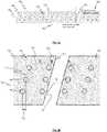
- Figures 4 and 5show an LED chip diced at an angle 60 of 76° relative to the transverse axis, or a typical orthogonal dicing line.
- the consecutive angle 62is 104° (i.e. 180° - 76°).
- the angle of dicing of the chipis dependent on the arrangement of the LEDs in the LED array, as explained above. This, in turn, allows for the pitch between LEDs on neighbouring chips to remain regular across an entire continuous LED array comprising a plurality of LED chips.
- the LEDshave a diameter in the range from 15 ⁇ m to 25 ⁇ m, or in specific LED chips, 20 ⁇ m.
- the longitudinal offset between corresponding LEDs in an LED arraymay be equal to the diameter of the LEDs, which may be 20 ⁇ m. In this way, the LEDs are aligned in the longitudinal axis to be one after the other with no space between.
- the transverse pitch between LEDs in adjacent rows of the LED arraymay be in the range from 10 um to 500 um, in the range from 70 ⁇ m to 90 ⁇ m or, in a specific LED chip, 80 ⁇ m. This results in a dicing angle of approximately 76°.
- This inventionallows for the fabrication of large arrays through the packaging together of smaller array chips. In an array the failure of a single pixel results in an un-useable chip. The effect of this on large chips is very wasteful. Therefore the approach of using smaller chips as building blocks for larger arrays allows for increased yields. It also allows for more economical positioning of chips on a wafer and the fabrication of arrays longer than the current diameter of a state-of-the-art GaN (visible LED) wafer - 150 mm.
- an array of LED chips as described hereinmay be manufactured. At least one LED chip 30a is positioned adjacent another LED chip 30b such that a longitudinal pitch 44 between adjacent LEDs on different chips is substantially the same as the longitudinal pitch 36a between adjacent LEDs on each chip. In specific LED arrays, a gap is defined between the adjacent chips.
- Traditional LED manufacturing techniqueinvolve the creation of discrete chips assembled into larger arrays on a wafer with pre-determined dicing lines or "streets" already present, which determine where the wafer will be diced. This in turn requires that the wafers be re-designed and manufactured specifically for each application or product.
- the dicing concept disclosed hereincould be applied across any point on a wafer. This means that the manufactured wafer can contain a large number of discrete LEDs (effectively pixels) without pre-determined dicing lines and that the wafer can be diced at any location. This creates the flexibility to generate different sized array chips from a common wafer layout, thereby simplifying manufacturing processes.
- LEDs placed closer to the edge of the dicing locationcan also confer benefits. Closer placement of the LED to the edge of the chips reduces the size of unused wafer at the edge of the die and thereby allows more tolerance between the chips during final assembly, as shown in Figure 3a . For example, if the LEDs are placed 100 microns apart on the wafer and a 50 micron dicing saw is used during the dicing stage, then the individual chips can allow a 50 micron gap between adjacent chips during the placement procedure, while still maintaining an overall 100 micron spacing between LEDs on adjacent chips. This 50 micron gap provides for higher tolerances during the assembly portion of the manufacturing process. With laser dicing this can be reduced to small gaps, while still maintaining adequate tolerances for industrial chips placement.
- an LED chipwhich is not square or rectangle in shape.
- the LED chipmay have angles formed by its corners of 90 degrees +/- 5 deg.
- the LED chipas may allow for the formation of an array of chips such that adjacent emitters on neighbouring chips are equidistant to adjacent emitters contained within a single chip.
- An LED arraycomprising individual chips packaged together, wherein the individual chips are diced at an angle other than 90°.
- the LEDmay comprise individual LED emitters arranged in a quasi 1D layout.
- the LED chipmay have an angle of dicing parallel to the line formed by the emitters adjacent to the edge.
- the LED array chipmay comprise a quasi-lD array that is unaffected by packaging constraints.
- the LED arraymay comprise LED chips as disclosed above which provide a continuous and uniform illumination source along the length of the array.
- the LED devicemay comprise individual emitters LEDs are ⁇ LEDs.
- the array of LEDsmay be on a wafer wherein there are no pre-determined dicing lines and the wafer may be diced at any point using a dicing angle other than 90° to give an array of any size.
- the array of LEDsmay be on a wafer wherein there are pre-determined dicing lines with the pitch between the neighbouring emitters being smaller than the normal pitch, thereby facilitating more tolerance in the placement of abutting chips.
- the methodcomprises fabricating an array of LEDs on a wafer substrate 70.
- the LEDs in a row of the arrayare longitudinally offset from corresponding LEDs in another row, as explained in detail above. Further, adjacent LEDs in each row of the array are separated by a longitudinal pitch, as explained in detail above.
- the methodfurther comprises dicing the wafer substrate 72 such that at least part of an end face of the substrate is angled with respect to a transverse axis of the LED chip, as explained in detail above. This allows the LED chip to be positionable adjacent another LED chip to maintain the longitudinal pitch between adjacent LEDs on different chips.
Landscapes
- Engineering & Computer Science (AREA)
- Microelectronics & Electronic Packaging (AREA)
- Physics & Mathematics (AREA)
- Power Engineering (AREA)
- Computer Hardware Design (AREA)
- General Physics & Mathematics (AREA)
- Condensed Matter Physics & Semiconductors (AREA)
- Optics & Photonics (AREA)
- Health & Medical Sciences (AREA)
- General Health & Medical Sciences (AREA)
- Toxicology (AREA)
- Geometry (AREA)
- Manufacturing & Machinery (AREA)
- Led Device Packages (AREA)
Abstract
Description
- The invention relates to a display, comprising a light emitting diode (LED) chip and a method of manufacturing a display comprising forming of an LED chip. More specifically, the invention relates to, but is not limited to, LED chips and methods of manufacturing LED chips that may be placed adjacent one another to form continuous arrays of LEDs.
- LEDs are a form of semiconductor material that convert electrical energy into optical energy. In semiconductor LEDs, light is typically generated through recombination of electrons, originating from an n-type doped semiconductor layer, and holes originating from a p-type doped semiconductor layer. In some infra-red emitting semiconductor materials light can be generated by electron intersub-band transitions rather than electron hole transitions.
- A major challenge in the field is to extract as much of the emitted light as possible from the semiconductor material into the surrounding medium, usually air. This is hindered by total internal reflection at the surfaces of the semiconductor.
- On traditional cuboid shaped LED chips, the average path length for light rays within the semiconductor is long, and the average number of reflections of an emitted light ray at semiconductor surfaces is high, prior to escape. Long path lengths and reflections at metal coated semiconductor surfaces may lead to absorption losses.
- A number of approaches have been applied to increase the amount of useful light from LEDs. These include the use of external reflecting mirrors and chip shaping. With all approaches there are also some associated drawbacks.
- A further approach to achieving high extraction efficiency (EE) and maximum useable light from a chip is to provide an array of "micro-LEDs" (µLEDs), as such devices keep the average path length within the device short. Arrangements are described in
US 6,410,940 andUS 6,410,942 . US 7,518, 149 describes a µLED that is an integrated diode structure in a mesa, in which the mesa shape and the light-emitting region are chosen for efficiency. A µLED may include, on a substrate and a semiconductor layer, a mesa, a light emitting layer, and an electrical contact. The µLEDs in this device may have improved EE because of their shape. Light is generated within the mesa, which is shaped to enhance the escape probability of the light. In particular, improved EEs may be achieved with a near parabolic mesa that has a high aspect ratio. The top of the mesa is truncated above the light-emitted layer (LEL), providing a flat surface for the electronic contact on the top of the semiconductor mesa. It has been found that the efficiency is improved, provided the top contact has a good reflectivity value.- The result of this structure is that the µLED output light is quasi-collimated, making the µLED a type of semiconductor light source that can be positioned somewhere between a Laser (where the light is coherent and directional) and a standard LED (where the light is scattered in all directions). These µLED devices allow for quasi collimated beams to be produced with a focus of, for example, less than 30°. This can be compared to standard unfocussed LEDs which produce beam angles in excess of 100°. The key benefits of being able to focus LED light is that less light is wasted because it is possible to get most or all the light generated by the LED into the space where it is needed, i.e. virtually all of the light generated is used, and little or none is wasted. This potentially results less power used by LED devices, which can lead to longer battery life in battery powered LED devices, and easier miniaturisation of devices as the light can be directed to where it is needed with the use of additional complicated optics.
- LED arrays have a number of applications including LED printing, heads-up displays, active matrix displays systems and signage, amongst others. They are distinct from standard LEDs in their ability to allow for individual emitters be controlled and switched independently. For wide format printing it may be required to provide a linear array light source of say 35cm or more wide, which are typically made up of a number of linear array modules. The linear array modules may be about 0.2 mm to 20 mm long and are abutted to form a longer linear array.
- Modular LED arrays are disclosed, for example, in
US 6,683,421 . - A problem encountered with available LED arrays, is that an array of individual LEDs on a chip may be closely spaced, but because of the packaging and housing surrounding such an array of LEDs, when two arrays (or chips) are abutted, the spacing between adjacent LEDs on the abutted chips can be quite large, much larger than the spacing between LEDs on the same chip. Similarly, high density square may use 5 x 5 diode arrays. These arrays may be arranged in groups to provide larger area high intensity arrays, for example as described in the above-mentioned
US 6,683, 421 . In another example, multiple LED arrays may be linearly arranged to provide a wide band of illumination. - In a typical square 5 x 5 LED array, for example, each LED die may be 1 mm2 so that the array may be about 7 mm x 7 mm. However, the arrays are fabricated on a substrate, which has a 1 mm to 2 mm edge that surrounds each individual LED die. The die may be hermetically sealed within the package, which requires a minimum wall thickness around the LEDs to provide a good seal. When these LED arrays are abutted, there is a gap or spacing between adjacent groups of LEDs, which may be 2 mm to 4 mm. Thus, there is a limit on the pitch between LEDs on the arrays to maintain the pitch across neighbouring arrays due to packaging constraints. This can mean that there is uniform intensity along the length or width of the each module, but there is a dip in intensity/irradiance in the region where each module abuts, which tends to cause a banding effect in the substrate being cured.
US 6,450,664 shows a modular LED array assembly, which provides a denser arrangement of LEDs near ends of the assembly to provide a uniform irradiance profile with a sharper edge, i.e. approaching a rectangular or "top hat" function.US 6,380,962 to Miyazaki provides an arrangement to provide an irradiance profile with a sharper edge using wider light source near ends of a linear light source. However, the problem of providing a more uniform irradiance profile where two modules abut is not addressed. In fact a sharp profile may exacerbate edge effects in modular arrays, i.e. creating a more marked discontinuity or dip in irradiance caused by the spacing where two modules abut, depending on the size of the gap or separation between LED elements due to the mechanical housing.- In another example, disclosed in
US 7,175,712 , LEDs are arranged in staggered rows, and LED arrays are also staggered to provide a more uniform irradiance. However, because of the thickness of the substrate and packaging surrounding the array, this arrangement also does not overcome a discontinuity in irradiance around edges of the arrays, or where two arrays abut. US 6,515,309 presents a method where grooves are cut below the top surface of the LED material such that a neighbouring chip may be closely aligned and packaging issues due to chipping are reduced. InUS 6,515,309 , the angled cuts are formed between the plane of the light emitting layer and the bottom of the chip (ie from top to bottom).WO 2010130051 provides a method for fabricating monolithic LED arrays with high resolution. It aims to replicate an addressable array of LED emitters that is continuous, i.e. contains no dark area. It is not possible simply to contact the individual emitters due to constraints on the interconnects. InWO 2010130051 , a constant array is replicated using two rows of emitters that are offset. This results in two complimentary rows which alternate between an emitting and a non-emitting area of the same size. In order to provide a constant line of light (i.e. a 1D array), the emitters are moved and timing of LED illumination is controlled.WO 2010130051 also outlines a control scheme and optical arrangement for use with the above arrays.- Arrays fabricated on individual standard LED chips cannot, in general, reach resolutions less than 200 µm. This is due to the limit on the size of the individual chips. Therefore to produce LED arrays of high density/resolution, monolithic array chips must be used. A similar problem of packing density and intensity occurs for monolithic arrays. Although the emitters can be very closely packaged when on the same chip, when multiple chips are abutted to form longer arrays the packaging density is reduced.
- With available LED arrays, for high speed printing applications using very short exposure times of the substrate to be cured, an array formed from individually packaged LED die, or a single row of LED die, may not provide sufficient intensity or resolution. It is then necessary to provide a higher density array of emitters to provide a line, a band, multiple lines, or multiple bands of illumination of higher intensity.
- Therefore, higher density arrays allow for faster printing or photo-curing and higher resolution printing as well as enabling a number of new applications.
- The inventors have identified a need for a modular LED array, which provides uniform irradiance over a large area, and avoids problems with a discontinuity in irradiance when two or more LED modules are abutted. Furthermore, the inventors have identified a need for an LED array which provides a continuous illumination source without the discontinuities which can occur when chips are abutted to form a longer array. Apparatus and methods disclosed herein allow for monolithic array chips to be abutted to form longer arrays without any loss of emitter density or resolution.
- Disclosed herein is a chip design that allows for enhanced packaging between individual chips. The inventors have appreciated that, in general, the distance between individual emitters must remain consistent across a full array, whether or not it includes multiple chips. Therefore in known arrays that contain multiple chips, the maximum resolution is dictated by the packaging constraints.
- According to an aspect of the invention, a display is provided, that comprises a light emitting diode (LED) chip, including a substrate; and an array of LEDs on the substrate arranged in a plurality of rows along a longitudinal direction of the substrate, LEDs in a row of the array being longitudinally offset from corresponding LEDs in another row, and adjacent LEDs in each row of the array being separated by the same longitudinal pitch, each of the LEDs having a diameter between 1 µm and 20 µm.. According to another aspect of the invention, a method of manufacturing a display is provided that comprises forming a light emitting diode (LED) chip including an array of LEDs on a substrate arranged in a plurality of rows along a longitudinal direction of the substrate, LEDs in a row of the array being longitudinally offset from corresponding LEDs in another row, and adjacent LEDs in each row of the array being separated by the same longitudinal pitch, each of the LEDs having a diameter between 1 um and 20 um.
- According to an embodiment of the invention, there may be provided an LED chip for use in an LED chip array forming a continuous array of LEDs. The LED chip may comprise an array of LEDs on a substrate. LEDs in a row of the array may be longitudinally offset from corresponding LEDs in another row. Adjacent LEDs in each row of the array may be separated by a longitudinal pitch. At least part of an end face of the substrate may be angled with respect to a transverse axis of the LED chip such that the LED chip is positionable adjacent another LED chip to maintain the longitudinal pitch between adjacent LEDs on different chips.
- The term "longitudinal" is used herein to define an axis of an LED chip and the term "transverse" is used herein to define another axis of an LED chip that is orthogonal to the longitudinal axis. However, it is noted that the terms are used only to make the description of the LED chip clearer and do not limit the relative dimensions of the LED chip. That is, the longitudinal axis need not define the longest axis of the LED chip. Further, the LED chip is not required to be elongate.
- It is noted that the end face of the substrate is angled with respect to the transverse axis. The end face may be substantially perpendicular to a top surface (i.e. a surface on which the LEDs are formed) and a bottom surface of the substrate. That is, the angled end face may produce a chamfered corner of the substrate when viewed from the top or bottom. The angular dice may be from one side to the other of the LED chip.
- As used herein, the term "corresponding LED" encompasses LEDs of an array that would, under normal square or rectangular array conditions, be in different rows but the same column. That is, in a square array, corresponding LEDs may be defined by a single column. It is noted that the terms "column" and "row" when referring to an array imply no limitation on the dimensions or orientation of an array and are used for descriptive purposes only.
- Optionally, the LEDs are arranged in a quasi 1-D array. A quasi 1-D array may comprise a plurality of LEDs in which the longitudinal offset between corresponding LEDs is equal to the diameter of each LED.
- Optionally, the LEDs comprise at least one µLED. The term "µLED" as used herein encompasses an LED emitter with a diameter in the range from 1 µm to 50 µm in diameter. A µLED may be a bottom emitter with light escaping through a bottom surface of the device. A µLED may include a reflective dome such that light is extracted with high efficiencies and in a controlled beam. Further definition of a µLED may be found in
US 7518149 . - Optionally, the angle of the at least part of the end face is based on the longitudinal offset between corresponding LEDs in different rows of the array and a transverse pitch between rows of the array.
- Optionally, the at least part of the end face of the substrate is substantially parallel to a line taken between corresponding LEDs in different rows of the array.
- Optionally, at least part of an opposite end face of the substrate is also angled with respect to the transverse axis.
- Optionally, the at least part of the end faces of the substrate are parallel.
- Optionally, the substrate forms a parallelogram.
- Optionally, each LED is a sufficient distance from an edge of the substrate such that light emitted from the LED does not substantially escape from the edge of the substrate. For example, each LED may be positioned a sufficient distance from the edge of the substrate such that the light escaping from the edge of the substrate is in a range from 0% to 50, in a range from 0% to 20, in a range from 0% to 10%, or in a range from 0% to 5%.
- Optionally, each LED is at least 5 µm from the edge of the substrate. Optionally, each LED may be at least 10 µm from the edge of the substrate.
- Optionally, the angle of the end face of the substrate relative to the transverse axis is in the range from 30 degrees to 85 degrees.
- According to a further embodiment of the invention, there may be provided an array of LED chips as defined above. At least one LED chip may be positioned adjacent another LED chip such that a longitudinal pitch between adjacent LEDs on different chips is substantially the same as the longitudinal pitch between adjacent LEDs on each chip.
- Optionally, a gap is defined between the adjacent chips.
- According to an embodiment of the invention, there is provided a method of manufacturing an LED chip. The method may comprise fabricating an array of LEDs on a wafer substrate. LEDs in a row of the array may be longitudinally offset from corresponding LEDs in another row, and adjacent LEDs in each row of the array may be separated by a longitudinal pitch. The method may further comprise dicing the wafer substrate such that at least part of an end face of the substrate is angled with respect to a transverse axis of the LED chip such that the LED chip is positionable adjacent another LED chip to maintain the longitudinal pitch between adjacent LEDs on different chips.
- Exemplary embodiments of the invention are described herein with reference to the accompanying drawings, in which:
Figure 1 a is a schematic representation of a 1-D array of LEDs on an LED chip;Figure 1 b is a schematic representation of two LED array chips positioned adjacent one another;Figure 2 is a schematic representation of a quasi 1-D array;Figure 3a is a schematic representation of two LED chips positioned adjacent one another;Figure 3b is an enlarged view of schematic representation of two LED chips positioned adjacent one another;Figure 4 is a schematic representation showing the angle of dicing of an LED chip;Figure 5 is a photograph of an LED chip; andFigure 6 is a flow diagram showing a method of manufacturing an LED chip.- Generally disclosed herein are apparatus and methods to allow LED chips to be positioned adjacent one another to form a continuous array of LEDs while maintaining a constant pitch between individual LEDs.
- LED arrays on an LED chip may comprise one or more of: 1) Discrete LED components (e.g. TO can, surface mount or epoxy packages) densely packed in a row on a PCB; 2) Bare die LED chips densely packed in a row (i.e. using Chip on Board (COB) or other approaches); and 3) Multiple individually addressable LEDs on a single chip (i.e. a monolithic LED array).
- For the first two examples above, a full LED chip produces light and each LED device in an array may be considered a single emitter. Therefore, the size of the LEDs and the pitch of such LEDs in an array (and hence the resolution) is defined by the size and packaging density of the individual components. For example, if a standard bare die LED chip with dimensions of 250 µm x 250 µm is used and requires a spacing of 200 µm interconnections, then the pixel size of an array so formed is limited to 250 µm and the pitch is limited to 200um.
- The production of individual LEDs of very small dimensions (say 100 µm or less) leads to significant problems with handling and interconnection of such chips. Therefore to produce arrays with LEDs of very small sizes it is required that array chips are formed. These are typically termed monolithic chips that have a number of areas that may or may not produce light. These allow for simpler handling and interconnection while enabling a small size of LED and pitch between LEDs.
- For the production of long arrays of this type, a single continuous piece of LED material is required. The length of such monolithic arrays is limited to approximately 200 mm due to the maximum diameter of an LED starter wafer. In practice, the maximum length of such arrays that can be fabricated is far smaller than this due to manufacturing tolerances and cost implications. In addition a single failed emitter on such a monolithic chip would result in the whole array being discarded. This has serious implications for yield and cost of manufacturing.
- To overcome these challenges and allow for long LED arrays in a cost effective manner a number of smaller monolithic LED array chips may be formed and packaged together to form a continuous LED array. In order to maintain a constant pitch between all LEDs in the continuous array, it is necessary to place adjacent chips as close together as possible so that the pitch between edge LEDs on two abutted chips is the same as the pitch between the emitters on the chips.
- Put another way, for the reasons given above, it is desirable that the pitch is constant between all LEDs in an LED array. This may be achieved fairly easily on a single chip. However, where longer arrays of LEDs are required, a plurality of LED chips, each comprising an array of LEDs, must be placed together to form a continuous array. In such cases, the pitch between the LEDs in the continuous array is limited to the minimum pitch that can be obtained between LEDs at the edges of adjacent LED array chips. Because of packaging constraints, the pitch between the LEDs at the edges of adjacent chips is required to be larger than is desired and unduly limits the pitch between all LEDs in the continuous array.
- This is demonstrated with reference to
Figures 1a and 1b. Figure 1a shows anLED chip 10 comprising asubstrate 12 and a 1-D array ofLEDs 14 formed on the substrate. The LEDs in thearray 14 are shown to be very tightly packed together and, in fact, the edges of each LED are touching the edges of each adjacent LED. Such arrays have applications in printing, heads-up displays, active matrix displays systems and signage, as described above. - Referring to
Figure 1b , an enlarged view of a firstLED array chip 10a positioned adjacent to a secondLED array chip 10b is shown. In practical applications, there is always an amount of substrate that remains to the side of theedge LEDs chips gap 16 is left in order to properly align the chips. Although inFigure 1 b the edge of the substrate is shown as a neat and straight line, typically, the cut edge of the substrate may be jagged and uneven or not completely flush. Therefore, if thechips chips gap 16, the pitch between theedge LED 14a and theedge LED 14b is not the same as the pitch between the LEDs on thechips - The apparatus and methods disclosed herein may be used with 1-D LED arrays. As such, this description focuses on 1-D arrays and, more specifically, quasi 1-D arrays (discussed below). However, it is noted that the principles disclosed herein may be applied to multi-dimensional arrays.
- Particular apparatus disclosed herein may comprise a quasi 1-D array of LEDs. A quasi 1-D array is described below with reference to
Figure 2 . A quasi 1-DLED array chip 20 comprises asubstrate 22 and a plurality ofLEDs 24 formed on the substrate. TheLEDs 24 are arranged in an array in which corresponding LEDs in different rows of the array are longitudinally offset. TheLEDs LEDs LED 24a andLED 24b is the same as the longitudinal offset betweenLED 24b andLED 24c. In the case ofFigure 2 , the array is slanted to form a parallelogram. - In practice, for quasi 1-D array chips the LEDs on a monolithic chip are offset in both directions to allow for simplification of the packaging and interconnection of the chips. This is shown in
Figure 2 by the empty circles, which show the position of an LED in a true 1-D array and the arrows, which show the offset of an LED. This is undertaken due to space requirements for contacting the emitters on the monolithic chips. In use, the quasi 1-D array chip is moved across a surface to be illuminated and the sequence of switching on the offset LEDs allows for the formation of a quasi 1-D array. - Apparatus and methods disclosed herein provide for dicing chips from a wafer in such a way that the pitch between LED emitters in an offset row on neighbouring chips is maintained. The approach is also suitable for the manufacture of 2D arrays with less wasted material and hence at lower cost.
- Cuts in two directions are required to release LED chips from a wafer. For standard applications, the cuts are at 90° to each other and the chip so formed is a square or a rectangle. In apparatus and methods disclosed herein, the cuts are not at 90° to each other. The shape formed by such a chip may be a parallelogram. In the specific example of a quasi 1-D array chip, the angle of the cut is defined by the size, pitch and displacement of the quasi 1-D array. In specific LED chips, the angle of the cut is parallel to a line between corresponding LEDs of the quasi 1-D array.
- Referring to
Figures 3a and 3b , anLED chip 30a is shown that is suitable for positioning adjacent to anotherLED chip 30b to form a continuous array of LEDs. TheLED chip 30a comprises asubstrate 32a having an array ofLEDs 34a formed thereon. In theexemplary chip 30a ofFigures 3a and 3b , the array ofLEDs 34a has three rows and thirteen columns. It will be appreciated that other configurations of rows and columns may be used. The LEDs in a row have alongitudinal pitch 36a between them. The longitudinal pitch is the distance from the centre of one LED to the centre of an adjacent LED in the same row. In addition, corresponding LEDs in adjacent rows are longitudinally offset 37a, as described above. The longitudinal offset is the distance from the centre of one LED to the centre of a corresponding LED in an adjacent row. - In exemplary LED chips, the diameter of the LEDs may be in the range from 1 µm to 50 µm or, in a specific exemplary LED chip, 20 µm. Such LEDs may be termed µLEDs.
- In the exemplary LED chip shown in
Figures 3a and 3b , the array of LEDs are arranged in a quasi-lD array, as described above. In such arrangements, thelongitudinal pitch 36a may be equivalent to a multiple of the diameter of the LEDs in the array. Specifically, thelongitudinal pitch 36a may be equal to the diameter of the LEDs in the array multiplied by the number of rows in the array minus one. That is, if the diameter of the LEDs is 20 µm and there are three rows in the LED array, the longitudinal pitch may be 40 µm. The longitudinal offset 37a may be equal to the diameter of the LEDs in the LED array. - A
longitudinal axis 38a and atransverse axis 40a are shown inFigure 3a for descriptive purposes only and do not imply any limitation on the shape of theLED chip 30a. - An
end face 42a of thesubstrate 32a is angled with respect to thetransverse axis 40a. This allows theLED chip 30a to be positioned adjacent anLED chip 30b in such a way that thelongitudinal pitch 44 between the LEDs on different chips is maintained. That is, thelongitudinal pitch 44 is substantially the same as thelongitudinal pitch 36a. In exemplary LED chips, the angle of theend face 42a of the substrate relative to thetransverse axis 40a may be in the range from 30 degrees to 85 degrees, or in the range from 70 degrees to 85 degrees, or in the range from 73 degrees to 79 degrees. - It is noted that the end face of the substrate is angled with respect to the transverse axis. The end face may be substantially perpendicular to a top surface (i.e. a surface on which the LEDs are formed) and a bottom surface of the substrate. That is, the angled end face may produce a chamfered corner of the substrate when viewed from the top or bottom. The angular dice may be from one side to the other of the LED chip.
- The
end face 42a may be any edge of the LED chip that is for positioning adjacent a corresponding edge face of another LED chip in an array of LED chips. - Because the
end face 42a of theLED chip 30a is angled and the corresponding end face of theLED chip 30b is also angled with respect to the transverse axis, thelongitudinal pitch 44 between the edge LEDs of thechips longitudinal pitch 36a between the LEDs on achip adjacent chips chips chips - In specific exemplary LED chips, the LEDs of the
LED array 34a comprise at least one µLED. In exemplary LED chips, the LEDs may comprise a cluster of a plurality of µLEDs. In a specific LED chip, the LEDs are µLEDs, as described inUS 7,518,149 . - The angle of the
end face 42a relative to thetransverse axis 40a is, in one exemplary LED chip, determined based on the longitudinal offset 37a between the corresponding LEDs of the array and atransverse pitch 46a between the rows of theLED array 34a. In one specific LED chip, theend face 42a of thesubstrate 32a is parallel to a line drawn between two corresponding LEDs in theLED array 34a. One way of calculating the angle of theend face 42a relative to thetransverse axis 40a is by determining the inverse tangent of thetransverse pitch 46a divided by the longitudinal offset 37a (tan-1(transversePitch/longitudinalOffset)). - As shown in
Figure 3a , anopposite end face 48a to theend face 42a may also be angled relative to thetransverse axis 40a. In specific LED chips, theopposite end face 48a may be parallel to theend face 42a. Insuch LED chips 30a, the substrate may be shaped substantially like a parallelogram. - In addition, an amount of
substrate 50a is left between the edge LEDs and theend face 42a of thesubstrate 32a. This is possible due to the tolerance available when placingLED chips angled end face 42a. The tolerance may be used to ensure that every LED is at least a given distance from the edge of thesubstrate 32a, which reduces loss of light emitted from an LED through the sides of the substrate. A similar section of substrate may also be seen onLED chip 30b. Figures 4 and 5 show an LED chip diced at anangle 60 of 76° relative to the transverse axis, or a typical orthogonal dicing line. Theconsecutive angle 62 is 104° (i.e. 180° - 76°). The angle of dicing of the chip is dependent on the arrangement of the LEDs in the LED array, as explained above. This, in turn, allows for the pitch between LEDs on neighbouring chips to remain regular across an entire continuous LED array comprising a plurality of LED chips.- In exemplary LED chips, the LEDs have a diameter in the range from 15 µm to 25 µm, or in specific LED chips, 20 µm. The longitudinal offset between corresponding LEDs in an LED array may be equal to the diameter of the LEDs, which may be 20 µm. In this way, the LEDs are aligned in the longitudinal axis to be one after the other with no space between. The transverse pitch between LEDs in adjacent rows of the LED array may be in the range from 10 um to 500 um, in the range from 70 µm to 90 µm or, in a specific LED chip, 80 µm. This results in a dicing angle of approximately 76°.
- This invention allows for the fabrication of large arrays through the packaging together of smaller array chips. In an array the failure of a single pixel results in an un-useable chip. The effect of this on large chips is very wasteful. Therefore the approach of using smaller chips as building blocks for larger arrays allows for increased yields. It also allows for more economical positioning of chips on a wafer and the fabrication of arrays longer than the current diameter of a state-of-the-art GaN (visible LED) wafer - 150 mm.
- As demonstrated by
Figures 3a and 3b , an array of LED chips as described herein may be manufactured. At least oneLED chip 30a is positioned adjacent anotherLED chip 30b such that alongitudinal pitch 44 between adjacent LEDs on different chips is substantially the same as thelongitudinal pitch 36a between adjacent LEDs on each chip. In specific LED arrays, a gap is defined between the adjacent chips. - Traditional LED manufacturing technique involve the creation of discrete chips assembled into larger arrays on a wafer with pre-determined dicing lines or "streets" already present, which determine where the wafer will be diced. This in turn requires that the wafers be re-designed and manufactured specifically for each application or product. The dicing concept disclosed herein could be applied across any point on a wafer. This means that the manufactured wafer can contain a large number of discrete LEDs (effectively pixels) without pre-determined dicing lines and that the wafer can be diced at any location. This creates the flexibility to generate different sized array chips from a common wafer layout, thereby simplifying manufacturing processes.
- Furthermore, having the LEDs placed closer to the edge of the dicing location can also confer benefits. Closer placement of the LED to the edge of the chips reduces the size of unused wafer at the edge of the die and thereby allows more tolerance between the chips during final assembly, as shown in
Figure 3a . For example, if the LEDs are placed 100 microns apart on the wafer and a 50 micron dicing saw is used during the dicing stage, then the individual chips can allow a 50 micron gap between adjacent chips during the placement procedure, while still maintaining an overall 100 micron spacing between LEDs on adjacent chips. This 50 micron gap provides for higher tolerances during the assembly portion of the manufacturing process. With laser dicing this can be reduced to small gaps, while still maintaining adequate tolerances for industrial chips placement. - Disclosed herein is an LED chip which is not square or rectangle in shape. The LED chip may have angles formed by its corners of 90 degrees +/- 5 deg. The LED chip as may allow for the formation of an array of chips such that adjacent emitters on neighbouring chips are equidistant to adjacent emitters contained within a single chip. An LED array comprising individual chips packaged together, wherein the individual chips are diced at an angle other than 90°. The LED may comprise individual LED emitters arranged in a quasi 1D layout. The LED chip may have an angle of dicing parallel to the line formed by the emitters adjacent to the edge. The LED array chip may comprise a quasi-lD array that is unaffected by packaging constraints. The LED array may comprise LED chips as disclosed above which provide a continuous and uniform illumination source along the length of the array. The LED device may comprise individual emitters LEDs are µLEDs. The array of LEDs may be on a wafer wherein there are no pre-determined dicing lines and the wafer may be diced at any point using a dicing angle other than 90° to give an array of any size. The array of LEDs may be on a wafer wherein there are pre-determined dicing lines with the pitch between the neighbouring emitters being smaller than the normal pitch, thereby facilitating more tolerance in the placement of abutting chips.
- There is also disclosed a method of manufacturing an LED chip, as shown in
Figure 6 . The method comprises fabricating an array of LEDs on awafer substrate 70. The LEDs in a row of the array are longitudinally offset from corresponding LEDs in another row, as explained in detail above. Further, adjacent LEDs in each row of the array are separated by a longitudinal pitch, as explained in detail above. The method further comprises dicing thewafer substrate 72 such that at least part of an end face of the substrate is angled with respect to a transverse axis of the LED chip, as explained in detail above. This allows the LED chip to be positionable adjacent another LED chip to maintain the longitudinal pitch between adjacent LEDs on different chips. - The skilled person will be able to envisage other methods and apparatus without departing from the scope of the appended claims.
Claims (15)
- A display, comprising:
a light emitting diode (LED) chip, including:a substrate; andan array of LEDs on the substrate arranged in a plurality of rows along a longitudinal direction of the substrate, LEDs in a row of the array being longitudinally offset from corresponding LEDs in another row, and adjacent LEDs in each row of the array being separated by the same longitudinal pitch, each of the LEDs having a diameter between 1 µm and 50 µm. - The display device of claim 1, wherein the longitudinal offset is equal to the diameter of the LEDs.
- The display of claim 1, wherein the longitudinal pitch corresponds to a multiple of the diameter of the LEDs.
- The display of claim 1, wherein the longitudinal offset is the same as the longitudinal pitch.
- The display of claim 1, wherein the substrate includes a first end face, at least a part of the first end face extending at a non-orthogonal angle relative to the longitudinal direction of the substrate, and the at least a part of the first end face being substantially parallel to a line taken between corresponding LEDs in different rows of the array of LEDs.
- The display of claim 1, wherein the substrate does not include a predetermined dicing line.
- The display of claim 1, further comprising another LED chip, and wherein the LED chip is placed adjacent to the other LED chip such that an LED on the LED chip and another LED on the other LED chip are separated by the longitudinal pitch.
- The display of claim 7, wherein the LED chip and the other LED chip are separated by a gap.
- The display of claim 1, wherein each LED is at least 5µm from an edge of the substrate.
- The display of claim 1, wherein each of the LEDs includes:a mesa having a parabolic shape with a truncated top; anda light emitting layer in the mesa.
- The electronic display device of claim1, wherein corresponding LEDs that are longitudinally offset in different rows correspond with an addressable column of the electronic display device.
- A method of manufacturing a display, comprising:
forming a light emitting diode (LED) chip including an array of LEDs on a substrate arranged in a plurality of rows along a longitudinal direction of the substrate, LEDs in a row of the array being longitudinally offset from corresponding LEDs in another row, and adjacent LEDs in each row of the array being separated by the same longitudinal pitch, each of the LEDs having a diameter between 1 µm and 50 µm. - The method of claim 12, wherein the longitudinal offset is equal to the diameter of the LEDs.
- The method of claim 12, wherein the longitudinal pitch corresponds to the multiple of a diameter of the LEDs.
- The method of claim 12, wherein the longitudinal offset is the same as the longitudinal pitch.
Applications Claiming Priority (3)
| Application Number | Priority Date | Filing Date | Title |
|---|---|---|---|
| US201261597236P | 2012-02-10 | 2012-02-10 | |
| PCT/EP2013/052690WO2013117760A1 (en) | 2012-02-10 | 2013-02-11 | Light emitting diode chip |
| EP13705746.9AEP2812928B1 (en) | 2012-02-10 | 2013-02-11 | Light emitting diode chip |
Related Parent Applications (1)
| Application Number | Title | Priority Date | Filing Date |
|---|---|---|---|
| EP13705746.9ADivisionEP2812928B1 (en) | 2012-02-10 | 2013-02-11 | Light emitting diode chip |
Publications (2)
| Publication Number | Publication Date |
|---|---|
| EP3528295A1true EP3528295A1 (en) | 2019-08-21 |
| EP3528295B1 EP3528295B1 (en) | 2021-04-07 |
Family
ID=47748589
Family Applications (2)
| Application Number | Title | Priority Date | Filing Date |
|---|---|---|---|
| EP19169273.0AActiveEP3528295B1 (en) | 2012-02-10 | 2013-02-11 | Display comprising led chip and method of manufacturing the same |
| EP13705746.9AActiveEP2812928B1 (en) | 2012-02-10 | 2013-02-11 | Light emitting diode chip |
Family Applications After (1)
| Application Number | Title | Priority Date | Filing Date |
|---|---|---|---|
| EP13705746.9AActiveEP2812928B1 (en) | 2012-02-10 | 2013-02-11 | Light emitting diode chip |
Country Status (3)
| Country | Link |
|---|---|
| US (3) | US9472594B2 (en) |
| EP (2) | EP3528295B1 (en) |
| WO (1) | WO2013117760A1 (en) |
Families Citing this family (5)
| Publication number | Priority date | Publication date | Assignee | Title |
|---|---|---|---|---|
| US9951935B2 (en)* | 2014-02-19 | 2018-04-24 | PA. COTTE Family Holding GmbH | Display device |
| DE102014009677A1 (en)* | 2014-02-19 | 2015-08-20 | Pierre-Alain Cotte | Display device with improved contrast |
| WO2017148491A1 (en) | 2016-03-02 | 2017-09-08 | Pa.Cotte Family Holding Gmbh | Method for producing a display device, and display device |
| JP6832666B2 (en)* | 2016-09-30 | 2021-02-24 | 株式会社ディスコ | Manufacturing method of semiconductor package |
| TWI742720B (en)* | 2020-06-12 | 2021-10-11 | 友達光電股份有限公司 | Display apparatus and manufacturing method thereof |
Citations (16)
| Publication number | Priority date | Publication date | Assignee | Title |
|---|---|---|---|---|
| US149A (en) | 1837-03-25 | Machine eoe cutting and heading wire foe the manufacture oe wood | ||
| US7518A (en) | 1850-07-22 | Improvement in fastening the shoes of hillside-plows | ||
| EP0142579A1 (en)* | 1983-11-01 | 1985-05-29 | Agfa-Gevaert N.V. | Recording apparatus |
| WO1990004853A1 (en)* | 1988-10-25 | 1990-05-03 | Prp Optoelectronics Limited | A print head |
| US5990494A (en)* | 1996-03-28 | 1999-11-23 | Fuji Xerox Co., Ltd. | Optoelectro transducer array, and light-emitting device array and fabrication process thereof |
| US6380962B1 (en) | 1998-12-21 | 2002-04-30 | Fuji Photo Film Co., Ltd. | Ray applying device |
| US6410942B1 (en) | 1999-12-03 | 2002-06-25 | Cree Lighting Company | Enhanced light extraction through the use of micro-LED arrays |
| US6410940B1 (en) | 2000-06-15 | 2002-06-25 | Kansas State University Research Foundation | Micro-size LED and detector arrays for minidisplay, hyper-bright light emitting diodes, lighting, and UV detector and imaging sensor applications |
| US6450664B1 (en) | 1999-10-01 | 2002-09-17 | Stockeryale (Irl) Limited | Linear illumination unit having plurality of LEDs |
| US6515309B1 (en) | 1998-12-25 | 2003-02-04 | Oki Electric Industry Co., Ltd. | LED array chip |
| US6683421B1 (en) | 2001-01-25 | 2004-01-27 | Exfo Photonic Solutions Inc. | Addressable semiconductor array light source for localized radiation delivery |
| US20050151828A1 (en)* | 2004-01-14 | 2005-07-14 | Xerox Corporation. | Xerographic printing system with VCSEL-micro-optic laser printbar |
| US7175712B2 (en) | 2003-01-09 | 2007-02-13 | Con-Trol-Cure, Inc. | Light emitting apparatus and method for curing inks, coatings and adhesives |
| US20080198592A1 (en)* | 2007-02-16 | 2008-08-21 | Canon Kabushiki Kaisha | Semiconductor light emitting device array chip and exposure light source apparatus |
| US7518149B2 (en) | 2003-05-02 | 2009-04-14 | University College Cork - National University Of Ireland, Cork | Light emitting mesa structures with high aspect ratio and near-parabolic sidewalls |
| WO2010130051A1 (en) | 2009-05-14 | 2010-11-18 | 4233999 Canada, Inc. | System for and method of providing high resolution images using monolithic arrays of light emitting diodes |
Family Cites Families (10)
| Publication number | Priority date | Publication date | Assignee | Title |
|---|---|---|---|---|
| US4728999A (en)* | 1980-06-25 | 1988-03-01 | Pitney Bowes Inc. | Light emitting diode assembly |
| US4729999A (en)* | 1984-10-12 | 1988-03-08 | Bcm Technologies | Antiestrogen therapy for symptoms of estrogen deficiency |
| US6163036A (en)* | 1997-09-15 | 2000-12-19 | Oki Data Corporation | Light emitting element module with a parallelogram-shaped chip and a staggered chip array |
| JP4868709B2 (en)* | 2004-03-09 | 2012-02-01 | 三洋電機株式会社 | Light emitting element |
| US7579204B2 (en)* | 2005-01-26 | 2009-08-25 | Sony Corporation | Method of production of semiconductor light emission device and method of production of light emission apparatus |
| US9172012B2 (en)* | 2007-10-31 | 2015-10-27 | Cree, Inc. | Multi-chip light emitter packages and related methods |
| US8937323B2 (en)* | 2011-09-02 | 2015-01-20 | Stanley Electric Co., Ltd. | LED array capable of reducing uneven brightness distribution |
| GB201202222D0 (en)* | 2012-02-09 | 2012-03-28 | Mled Ltd | Enhanced light extraction |
| DE102012008638A1 (en)* | 2012-05-02 | 2013-11-07 | Heraeus Noblelight Gmbh | Luminaire with LEDs and cylindrical lens |
| US9755126B2 (en)* | 2012-07-30 | 2017-09-05 | Ushio Denki Kabushiki Kaisha | Light source unit |
- 2013
- 2013-02-11USUS14/377,731patent/US9472594B2/enactiveActive
- 2013-02-11EPEP19169273.0Apatent/EP3528295B1/enactiveActive
- 2013-02-11WOPCT/EP2013/052690patent/WO2013117760A1/enactiveApplication Filing
- 2013-02-11EPEP13705746.9Apatent/EP2812928B1/enactiveActive
- 2016
- 2016-09-15USUS15/267,080patent/US9917136B2/enactiveActive
- 2018
- 2018-01-30USUS15/884,250patent/US10121823B2/enactiveActive
Patent Citations (16)
| Publication number | Priority date | Publication date | Assignee | Title |
|---|---|---|---|---|
| US149A (en) | 1837-03-25 | Machine eoe cutting and heading wire foe the manufacture oe wood | ||
| US7518A (en) | 1850-07-22 | Improvement in fastening the shoes of hillside-plows | ||
| EP0142579A1 (en)* | 1983-11-01 | 1985-05-29 | Agfa-Gevaert N.V. | Recording apparatus |
| WO1990004853A1 (en)* | 1988-10-25 | 1990-05-03 | Prp Optoelectronics Limited | A print head |
| US5990494A (en)* | 1996-03-28 | 1999-11-23 | Fuji Xerox Co., Ltd. | Optoelectro transducer array, and light-emitting device array and fabrication process thereof |
| US6380962B1 (en) | 1998-12-21 | 2002-04-30 | Fuji Photo Film Co., Ltd. | Ray applying device |
| US6515309B1 (en) | 1998-12-25 | 2003-02-04 | Oki Electric Industry Co., Ltd. | LED array chip |
| US6450664B1 (en) | 1999-10-01 | 2002-09-17 | Stockeryale (Irl) Limited | Linear illumination unit having plurality of LEDs |
| US6410942B1 (en) | 1999-12-03 | 2002-06-25 | Cree Lighting Company | Enhanced light extraction through the use of micro-LED arrays |
| US6410940B1 (en) | 2000-06-15 | 2002-06-25 | Kansas State University Research Foundation | Micro-size LED and detector arrays for minidisplay, hyper-bright light emitting diodes, lighting, and UV detector and imaging sensor applications |
| US6683421B1 (en) | 2001-01-25 | 2004-01-27 | Exfo Photonic Solutions Inc. | Addressable semiconductor array light source for localized radiation delivery |
| US7175712B2 (en) | 2003-01-09 | 2007-02-13 | Con-Trol-Cure, Inc. | Light emitting apparatus and method for curing inks, coatings and adhesives |
| US7518149B2 (en) | 2003-05-02 | 2009-04-14 | University College Cork - National University Of Ireland, Cork | Light emitting mesa structures with high aspect ratio and near-parabolic sidewalls |
| US20050151828A1 (en)* | 2004-01-14 | 2005-07-14 | Xerox Corporation. | Xerographic printing system with VCSEL-micro-optic laser printbar |
| US20080198592A1 (en)* | 2007-02-16 | 2008-08-21 | Canon Kabushiki Kaisha | Semiconductor light emitting device array chip and exposure light source apparatus |
| WO2010130051A1 (en) | 2009-05-14 | 2010-11-18 | 4233999 Canada, Inc. | System for and method of providing high resolution images using monolithic arrays of light emitting diodes |
Also Published As
| Publication number | Publication date |
|---|---|
| US9472594B2 (en) | 2016-10-18 |
| EP3528295B1 (en) | 2021-04-07 |
| US20170005134A1 (en) | 2017-01-05 |
| US9917136B2 (en) | 2018-03-13 |
| US20180158866A1 (en) | 2018-06-07 |
| EP2812928A1 (en) | 2014-12-17 |
| US10121823B2 (en) | 2018-11-06 |
| EP2812928B1 (en) | 2019-04-17 |
| WO2013117760A1 (en) | 2013-08-15 |
| US20150028366A1 (en) | 2015-01-29 |
Similar Documents
| Publication | Publication Date | Title |
|---|---|---|
| US10121823B2 (en) | Light emitting diode chip | |
| JP5657563B2 (en) | Optoelectronic projection apparatus and manufacturing method thereof | |
| CN109075184B (en) | led | |
| JP6261718B2 (en) | Light emitting semiconductor device and method for manufacturing light emitting semiconductor device | |
| US20130207139A1 (en) | Radiation-emitting component and method for producing radiation-emitting components | |
| JP2005327979A (en) | Semiconductor light emitting element and semiconductor light emitting device | |
| KR102608856B1 (en) | Flip-chip SMT LEDs with variable number of emitting surfaces | |
| US12046704B2 (en) | Packaged ultraviolet light-emitting device and production method thereof | |
| US20190181309A1 (en) | Cutting method of semiconductor package module and semiconductor package unit | |
| US8294175B2 (en) | Light-emitting device and display | |
| KR102417580B1 (en) | Light emitting device, light emitting module, manufacturing method for light emitting device and munufacturing method for light emitting module | |
| KR20110099751A (en) | Light emitting device | |
| CN102856460A (en) | Light-emitting diode element, its manufacturing method, and light-emitting device | |
| US9899359B1 (en) | Light emitting diode package structure, method for making the same, and flat panel light source having the same | |
| US20160226223A1 (en) | VCSEL Packaging and VCSEL Array Configurations | |
| JP5334734B2 (en) | Light emitting device | |
| EP4249967A1 (en) | Light-emitting device and manufacturing method therefor | |
| CN106575691A (en) | Semiconductor component, illuminating device, and method for producing a semiconductor component | |
| EP2943985B1 (en) | Shaped led for enhanced light extraction efficiency | |
| US11848196B2 (en) | Light-emitting diode package having controlled beam angle and light-emitting device using same | |
| JP7245003B2 (en) | semiconductor light emitting device | |
| KR20130049896A (en) | Light emitting device manufacturing method and lead frame base material used for the same | |
| JP5334733B2 (en) | Light emitting device | |
| KR20160000624A (en) | Method for manufacturing direct bonded chip scale packaged light emitting diode | |
| TW202535214A (en) | Laser package structure |
Legal Events
| Date | Code | Title | Description |
|---|---|---|---|
| PUAI | Public reference made under article 153(3) epc to a published international application that has entered the european phase | Free format text:ORIGINAL CODE: 0009012 | |
| STAA | Information on the status of an ep patent application or granted ep patent | Free format text:STATUS: THE APPLICATION HAS BEEN PUBLISHED | |
| AC | Divisional application: reference to earlier application | Ref document number:2812928 Country of ref document:EP Kind code of ref document:P | |
| AK | Designated contracting states | Kind code of ref document:A1 Designated state(s):AL AT BE BG CH CY CZ DE DK EE ES FI FR GB GR HR HU IE IS IT LI LT LU LV MC MK MT NL NO PL PT RO RS SE SI SK SM TR | |
| STAA | Information on the status of an ep patent application or granted ep patent | Free format text:STATUS: REQUEST FOR EXAMINATION WAS MADE | |
| 17P | Request for examination filed | Effective date:20200220 | |
| RBV | Designated contracting states (corrected) | Designated state(s):AL AT BE BG CH CY CZ DE DK EE ES FI FR GB GR HR HU IE IS IT LI LT LU LV MC MK MT NL NO PL PT RO RS SE SI SK SM TR | |
| GRAP | Despatch of communication of intention to grant a patent | Free format text:ORIGINAL CODE: EPIDOSNIGR1 | |
| STAA | Information on the status of an ep patent application or granted ep patent | Free format text:STATUS: GRANT OF PATENT IS INTENDED | |
| RIC1 | Information provided on ipc code assigned before grant | Ipc:H01L 33/20 20100101AFI20200911BHEP Ipc:H01L 25/075 20060101ALN20200911BHEP Ipc:H01L 27/15 20060101ALN20200911BHEP Ipc:B41J 2/45 20060101ALI20200911BHEP | |
| INTG | Intention to grant announced | Effective date:20200929 | |
| GRAS | Grant fee paid | Free format text:ORIGINAL CODE: EPIDOSNIGR3 | |
| GRAA | (expected) grant | Free format text:ORIGINAL CODE: 0009210 | |
| STAA | Information on the status of an ep patent application or granted ep patent | Free format text:STATUS: THE PATENT HAS BEEN GRANTED | |
| AC | Divisional application: reference to earlier application | Ref document number:2812928 Country of ref document:EP Kind code of ref document:P | |
| AK | Designated contracting states | Kind code of ref document:B1 Designated state(s):AL AT BE BG CH CY CZ DE DK EE ES FI FR GB GR HR HU IE IS IT LI LT LU LV MC MK MT NL NO PL PT RO RS SE SI SK SM TR | |
| REG | Reference to a national code | Ref country code:GB Ref legal event code:FG4D | |
| REG | Reference to a national code | Ref country code:AT Ref legal event code:REF Ref document number:1380813 Country of ref document:AT Kind code of ref document:T Effective date:20210415 Ref country code:CH Ref legal event code:EP | |
| REG | Reference to a national code | Ref country code:DE Ref legal event code:R096 Ref document number:602013076852 Country of ref document:DE | |
| REG | Reference to a national code | Ref country code:IE Ref legal event code:FG4D | |
| REG | Reference to a national code | Ref country code:LT Ref legal event code:MG9D | |
| REG | Reference to a national code | Ref country code:NL Ref legal event code:MP Effective date:20210407 Ref country code:AT Ref legal event code:MK05 Ref document number:1380813 Country of ref document:AT Kind code of ref document:T Effective date:20210407 | |
| PG25 | Lapsed in a contracting state [announced via postgrant information from national office to epo] | Ref country code:LT Free format text:LAPSE BECAUSE OF FAILURE TO SUBMIT A TRANSLATION OF THE DESCRIPTION OR TO PAY THE FEE WITHIN THE PRESCRIBED TIME-LIMIT Effective date:20210407 Ref country code:HR Free format text:LAPSE BECAUSE OF FAILURE TO SUBMIT A TRANSLATION OF THE DESCRIPTION OR TO PAY THE FEE WITHIN THE PRESCRIBED TIME-LIMIT Effective date:20210407 Ref country code:FI Free format text:LAPSE BECAUSE OF FAILURE TO SUBMIT A TRANSLATION OF THE DESCRIPTION OR TO PAY THE FEE WITHIN THE PRESCRIBED TIME-LIMIT Effective date:20210407 Ref country code:BG Free format text:LAPSE BECAUSE OF FAILURE TO SUBMIT A TRANSLATION OF THE DESCRIPTION OR TO PAY THE FEE WITHIN THE PRESCRIBED TIME-LIMIT Effective date:20210707 Ref country code:AT Free format text:LAPSE BECAUSE OF FAILURE TO SUBMIT A TRANSLATION OF THE DESCRIPTION OR TO PAY THE FEE WITHIN THE PRESCRIBED TIME-LIMIT Effective date:20210407 Ref country code:NL Free format text:LAPSE BECAUSE OF FAILURE TO SUBMIT A TRANSLATION OF THE DESCRIPTION OR TO PAY THE FEE WITHIN THE PRESCRIBED TIME-LIMIT Effective date:20210407 | |
| PG25 | Lapsed in a contracting state [announced via postgrant information from national office to epo] | Ref country code:GR Free format text:LAPSE BECAUSE OF FAILURE TO SUBMIT A TRANSLATION OF THE DESCRIPTION OR TO PAY THE FEE WITHIN THE PRESCRIBED TIME-LIMIT Effective date:20210708 Ref country code:IS Free format text:LAPSE BECAUSE OF FAILURE TO SUBMIT A TRANSLATION OF THE DESCRIPTION OR TO PAY THE FEE WITHIN THE PRESCRIBED TIME-LIMIT Effective date:20210807 Ref country code:PT Free format text:LAPSE BECAUSE OF FAILURE TO SUBMIT A TRANSLATION OF THE DESCRIPTION OR TO PAY THE FEE WITHIN THE PRESCRIBED TIME-LIMIT Effective date:20210809 Ref country code:RS Free format text:LAPSE BECAUSE OF FAILURE TO SUBMIT A TRANSLATION OF THE DESCRIPTION OR TO PAY THE FEE WITHIN THE PRESCRIBED TIME-LIMIT Effective date:20210407 Ref country code:SE Free format text:LAPSE BECAUSE OF FAILURE TO SUBMIT A TRANSLATION OF THE DESCRIPTION OR TO PAY THE FEE WITHIN THE PRESCRIBED TIME-LIMIT Effective date:20210407 Ref country code:LV Free format text:LAPSE BECAUSE OF FAILURE TO SUBMIT A TRANSLATION OF THE DESCRIPTION OR TO PAY THE FEE WITHIN THE PRESCRIBED TIME-LIMIT Effective date:20210407 Ref country code:PL Free format text:LAPSE BECAUSE OF FAILURE TO SUBMIT A TRANSLATION OF THE DESCRIPTION OR TO PAY THE FEE WITHIN THE PRESCRIBED TIME-LIMIT Effective date:20210407 Ref country code:NO Free format text:LAPSE BECAUSE OF FAILURE TO SUBMIT A TRANSLATION OF THE DESCRIPTION OR TO PAY THE FEE WITHIN THE PRESCRIBED TIME-LIMIT Effective date:20210707 | |
| REG | Reference to a national code | Ref country code:DE Ref legal event code:R097 Ref document number:602013076852 Country of ref document:DE | |
| PG25 | Lapsed in a contracting state [announced via postgrant information from national office to epo] | Ref country code:SK Free format text:LAPSE BECAUSE OF FAILURE TO SUBMIT A TRANSLATION OF THE DESCRIPTION OR TO PAY THE FEE WITHIN THE PRESCRIBED TIME-LIMIT Effective date:20210407 Ref country code:EE Free format text:LAPSE BECAUSE OF FAILURE TO SUBMIT A TRANSLATION OF THE DESCRIPTION OR TO PAY THE FEE WITHIN THE PRESCRIBED TIME-LIMIT Effective date:20210407 Ref country code:ES Free format text:LAPSE BECAUSE OF FAILURE TO SUBMIT A TRANSLATION OF THE DESCRIPTION OR TO PAY THE FEE WITHIN THE PRESCRIBED TIME-LIMIT Effective date:20210407 Ref country code:SM Free format text:LAPSE BECAUSE OF FAILURE TO SUBMIT A TRANSLATION OF THE DESCRIPTION OR TO PAY THE FEE WITHIN THE PRESCRIBED TIME-LIMIT Effective date:20210407 Ref country code:RO Free format text:LAPSE BECAUSE OF FAILURE TO SUBMIT A TRANSLATION OF THE DESCRIPTION OR TO PAY THE FEE WITHIN THE PRESCRIBED TIME-LIMIT Effective date:20210407 Ref country code:DK Free format text:LAPSE BECAUSE OF FAILURE TO SUBMIT A TRANSLATION OF THE DESCRIPTION OR TO PAY THE FEE WITHIN THE PRESCRIBED TIME-LIMIT Effective date:20210407 Ref country code:CZ Free format text:LAPSE BECAUSE OF FAILURE TO SUBMIT A TRANSLATION OF THE DESCRIPTION OR TO PAY THE FEE WITHIN THE PRESCRIBED TIME-LIMIT Effective date:20210407 | |
| PLBE | No opposition filed within time limit | Free format text:ORIGINAL CODE: 0009261 | |
| STAA | Information on the status of an ep patent application or granted ep patent | Free format text:STATUS: NO OPPOSITION FILED WITHIN TIME LIMIT | |
| 26N | No opposition filed | Effective date:20220110 | |
| PG25 | Lapsed in a contracting state [announced via postgrant information from national office to epo] | Ref country code:IS Free format text:LAPSE BECAUSE OF FAILURE TO SUBMIT A TRANSLATION OF THE DESCRIPTION OR TO PAY THE FEE WITHIN THE PRESCRIBED TIME-LIMIT Effective date:20210807 Ref country code:AL Free format text:LAPSE BECAUSE OF FAILURE TO SUBMIT A TRANSLATION OF THE DESCRIPTION OR TO PAY THE FEE WITHIN THE PRESCRIBED TIME-LIMIT Effective date:20210407 | |
| PG25 | Lapsed in a contracting state [announced via postgrant information from national office to epo] | Ref country code:IT Free format text:LAPSE BECAUSE OF FAILURE TO SUBMIT A TRANSLATION OF THE DESCRIPTION OR TO PAY THE FEE WITHIN THE PRESCRIBED TIME-LIMIT Effective date:20210407 | |
| PG25 | Lapsed in a contracting state [announced via postgrant information from national office to epo] | Ref country code:MC Free format text:LAPSE BECAUSE OF FAILURE TO SUBMIT A TRANSLATION OF THE DESCRIPTION OR TO PAY THE FEE WITHIN THE PRESCRIBED TIME-LIMIT Effective date:20210407 | |
| REG | Reference to a national code | Ref country code:CH Ref legal event code:PL | |
| REG | Reference to a national code | Ref country code:BE Ref legal event code:MM Effective date:20220228 | |
| PG25 | Lapsed in a contracting state [announced via postgrant information from national office to epo] | Ref country code:LU Free format text:LAPSE BECAUSE OF NON-PAYMENT OF DUE FEES Effective date:20220211 | |
| PG25 | Lapsed in a contracting state [announced via postgrant information from national office to epo] | Ref country code:LI Free format text:LAPSE BECAUSE OF NON-PAYMENT OF DUE FEES Effective date:20220228 Ref country code:IE Free format text:LAPSE BECAUSE OF NON-PAYMENT OF DUE FEES Effective date:20220211 Ref country code:CH Free format text:LAPSE BECAUSE OF NON-PAYMENT OF DUE FEES Effective date:20220228 | |
| PG25 | Lapsed in a contracting state [announced via postgrant information from national office to epo] | Ref country code:BE Free format text:LAPSE BECAUSE OF NON-PAYMENT OF DUE FEES Effective date:20220228 | |
| P01 | Opt-out of the competence of the unified patent court (upc) registered | Effective date:20230525 | |
| REG | Reference to a national code | Ref country code:DE Ref legal event code:R081 Ref document number:602013076852 Country of ref document:DE Owner name:META PLATFORMS TECHNOLOGIES, LLC, MENLO PARK, US Free format text:FORMER OWNER: FACEBOOK TECHNOLOGIES, LLC, MENLO PARK, CALIF., US | |
| PG25 | Lapsed in a contracting state [announced via postgrant information from national office to epo] | Ref country code:MK Free format text:LAPSE BECAUSE OF FAILURE TO SUBMIT A TRANSLATION OF THE DESCRIPTION OR TO PAY THE FEE WITHIN THE PRESCRIBED TIME-LIMIT Effective date:20210407 Ref country code:CY Free format text:LAPSE BECAUSE OF FAILURE TO SUBMIT A TRANSLATION OF THE DESCRIPTION OR TO PAY THE FEE WITHIN THE PRESCRIBED TIME-LIMIT Effective date:20210407 | |
| PGFP | Annual fee paid to national office [announced via postgrant information from national office to epo] | Ref country code:DE Payment date:20240226 Year of fee payment:12 Ref country code:GB Payment date:20240229 Year of fee payment:12 | |
| PG25 | Lapsed in a contracting state [announced via postgrant information from national office to epo] | Ref country code:HU Free format text:LAPSE BECAUSE OF FAILURE TO SUBMIT A TRANSLATION OF THE DESCRIPTION OR TO PAY THE FEE WITHIN THE PRESCRIBED TIME-LIMIT; INVALID AB INITIO Effective date:20130211 | |
| PGFP | Annual fee paid to national office [announced via postgrant information from national office to epo] | Ref country code:FR Payment date:20240222 Year of fee payment:12 | |
| PG25 | Lapsed in a contracting state [announced via postgrant information from national office to epo] | Ref country code:TR Free format text:LAPSE BECAUSE OF FAILURE TO SUBMIT A TRANSLATION OF THE DESCRIPTION OR TO PAY THE FEE WITHIN THE PRESCRIBED TIME-LIMIT Effective date:20210407 | |
| PG25 | Lapsed in a contracting state [announced via postgrant information from national office to epo] | Ref country code:MT Free format text:LAPSE BECAUSE OF FAILURE TO SUBMIT A TRANSLATION OF THE DESCRIPTION OR TO PAY THE FEE WITHIN THE PRESCRIBED TIME-LIMIT Effective date:20210407 | |
| REG | Reference to a national code | Ref country code:DE Ref legal event code:R079 Ref document number:602013076852 Country of ref document:DE Free format text:PREVIOUS MAIN CLASS: H01L0033200000 Ipc:H10H0020819000 |