EP3512218B1 - Common wave and sideband mitigation communication systems and methods for increasing communication speeds,spectral efficiency and enabling other benefits - Google Patents
Common wave and sideband mitigation communication systems and methods for increasing communication speeds,spectral efficiency and enabling other benefitsDownload PDFInfo
- Publication number
- EP3512218B1 EP3512218B1EP19154144.0AEP19154144AEP3512218B1EP 3512218 B1EP3512218 B1EP 3512218B1EP 19154144 AEP19154144 AEP 19154144AEP 3512218 B1EP3512218 B1EP 3512218B1
- Authority
- EP
- European Patent Office
- Prior art keywords
- signal
- carrier wave
- data
- phase
- wave
- Prior art date
- Legal status (The legal status is an assumption and is not a legal conclusion. Google has not performed a legal analysis and makes no representation as to the accuracy of the status listed.)
- Active
Links
Images


Classifications
- H—ELECTRICITY
- H04—ELECTRIC COMMUNICATION TECHNIQUE
- H04L—TRANSMISSION OF DIGITAL INFORMATION, e.g. TELEGRAPHIC COMMUNICATION
- H04L25/00—Baseband systems
- H04L25/02—Details ; arrangements for supplying electrical power along data transmission lines
- H04L25/03—Shaping networks in transmitter or receiver, e.g. adaptive shaping networks
- H04L25/03006—Arrangements for removing intersymbol interference
- H04L25/03178—Arrangements involving sequence estimation techniques
- H04L25/03248—Arrangements for operating in conjunction with other apparatus
- H04L25/03273—Arrangements for operating in conjunction with other apparatus with carrier recovery circuitry
- H—ELECTRICITY
- H04—ELECTRIC COMMUNICATION TECHNIQUE
- H04L—TRANSMISSION OF DIGITAL INFORMATION, e.g. TELEGRAPHIC COMMUNICATION
- H04L27/00—Modulated-carrier systems
- H04L27/18—Phase-modulated carrier systems, i.e. using phase-shift keying
- H04L27/22—Demodulator circuits; Receiver circuits
- H—ELECTRICITY
- H04—ELECTRIC COMMUNICATION TECHNIQUE
- H04B—TRANSMISSION
- H04B13/00—Transmission systems characterised by the medium used for transmission, not provided for in groups H04B3/00 - H04B11/00
- H04B13/02—Transmission systems in which the medium consists of the earth or a large mass of water thereon, e.g. earth telegraphy
- H—ELECTRICITY
- H04—ELECTRIC COMMUNICATION TECHNIQUE
- H04B—TRANSMISSION
- H04B1/00—Details of transmission systems, not covered by a single one of groups H04B3/00 - H04B13/00; Details of transmission systems not characterised by the medium used for transmission
- H04B1/62—Details of transmission systems, not covered by a single one of groups H04B3/00 - H04B13/00; Details of transmission systems not characterised by the medium used for transmission for providing a predistortion of the signal in the transmitter and corresponding correction in the receiver, e.g. for improving the signal/noise ratio
- H—ELECTRICITY
- H04—ELECTRIC COMMUNICATION TECHNIQUE
- H04B—TRANSMISSION
- H04B3/00—Line transmission systems
- H04B3/02—Details
- H04B3/04—Control of transmission; Equalising
- H04B3/10—Control of transmission; Equalising by pilot signal
- H—ELECTRICITY
- H04—ELECTRIC COMMUNICATION TECHNIQUE
- H04L—TRANSMISSION OF DIGITAL INFORMATION, e.g. TELEGRAPHIC COMMUNICATION
- H04L25/00—Baseband systems
- H04L25/02—Details ; arrangements for supplying electrical power along data transmission lines
- H04L25/0264—Arrangements for coupling to transmission lines
- H04L25/0298—Arrangement for terminating transmission lines
- H—ELECTRICITY
- H04—ELECTRIC COMMUNICATION TECHNIQUE
- H04L—TRANSMISSION OF DIGITAL INFORMATION, e.g. TELEGRAPHIC COMMUNICATION
- H04L25/00—Baseband systems
- H04L25/02—Details ; arrangements for supplying electrical power along data transmission lines
- H04L25/03—Shaping networks in transmitter or receiver, e.g. adaptive shaping networks
- H04L25/03006—Arrangements for removing intersymbol interference
- H—ELECTRICITY
- H04—ELECTRIC COMMUNICATION TECHNIQUE
- H04L—TRANSMISSION OF DIGITAL INFORMATION, e.g. TELEGRAPHIC COMMUNICATION
- H04L25/00—Baseband systems
- H04L25/02—Details ; arrangements for supplying electrical power along data transmission lines
- H04L25/03—Shaping networks in transmitter or receiver, e.g. adaptive shaping networks
- H04L25/03828—Arrangements for spectral shaping; Arrangements for providing signals with specified spectral properties
- H04L25/03866—Arrangements for spectral shaping; Arrangements for providing signals with specified spectral properties using scrambling
- H—ELECTRICITY
- H04—ELECTRIC COMMUNICATION TECHNIQUE
- H04L—TRANSMISSION OF DIGITAL INFORMATION, e.g. TELEGRAPHIC COMMUNICATION
- H04L25/00—Baseband systems
- H04L25/02—Details ; arrangements for supplying electrical power along data transmission lines
- H04L25/08—Modifications for reducing interference; Modifications for reducing effects due to line faults ; Receiver end arrangements for detecting or overcoming line faults
- H—ELECTRICITY
- H04—ELECTRIC COMMUNICATION TECHNIQUE
- H04L—TRANSMISSION OF DIGITAL INFORMATION, e.g. TELEGRAPHIC COMMUNICATION
- H04L27/00—Modulated-carrier systems
- H04L27/18—Phase-modulated carrier systems, i.e. using phase-shift keying
- H—ELECTRICITY
- H04—ELECTRIC COMMUNICATION TECHNIQUE
- H04L—TRANSMISSION OF DIGITAL INFORMATION, e.g. TELEGRAPHIC COMMUNICATION
- H04L27/00—Modulated-carrier systems
- H04L27/32—Carrier systems characterised by combinations of two or more of the types covered by groups H04L27/02, H04L27/10, H04L27/18 or H04L27/26
- H04L27/34—Amplitude- and phase-modulated carrier systems, e.g. quadrature-amplitude modulated carrier systems
- H—ELECTRICITY
- H04—ELECTRIC COMMUNICATION TECHNIQUE
- H04L—TRANSMISSION OF DIGITAL INFORMATION, e.g. TELEGRAPHIC COMMUNICATION
- H04L7/00—Arrangements for synchronising receiver with transmitter
- H04L7/02—Speed or phase control by the received code signals, the signals containing no special synchronisation information
- H04L7/033—Speed or phase control by the received code signals, the signals containing no special synchronisation information using the transitions of the received signal to control the phase of the synchronising-signal-generating means, e.g. using a phase-locked loop
- H04L7/0331—Speed or phase control by the received code signals, the signals containing no special synchronisation information using the transitions of the received signal to control the phase of the synchronising-signal-generating means, e.g. using a phase-locked loop with a digital phase-locked loop [PLL] processing binary samples, e.g. add/subtract logic for correction of receiver clock
- H—ELECTRICITY
- H04—ELECTRIC COMMUNICATION TECHNIQUE
- H04L—TRANSMISSION OF DIGITAL INFORMATION, e.g. TELEGRAPHIC COMMUNICATION
- H04L25/00—Baseband systems
- H04L25/02—Details ; arrangements for supplying electrical power along data transmission lines
- H04L25/03—Shaping networks in transmitter or receiver, e.g. adaptive shaping networks
- H04L25/03006—Arrangements for removing intersymbol interference
- H04L2025/0335—Arrangements for removing intersymbol interference characterised by the type of transmission
- H04L2025/03356—Baseband transmission
- H—ELECTRICITY
- H04—ELECTRIC COMMUNICATION TECHNIQUE
- H04L—TRANSMISSION OF DIGITAL INFORMATION, e.g. TELEGRAPHIC COMMUNICATION
- H04L25/00—Baseband systems
- H04L25/02—Details ; arrangements for supplying electrical power along data transmission lines
- H04L25/03—Shaping networks in transmitter or receiver, e.g. adaptive shaping networks
- H04L25/03006—Arrangements for removing intersymbol interference
- H04L2025/0335—Arrangements for removing intersymbol interference characterised by the type of transmission
- H04L2025/03375—Passband transmission
- H04L2025/03382—Single of vestigal sideband
Definitions
- a wired or wireless communication system and methodare provided.
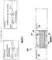
- FIG. 1two different conventional communication systems are known.
- a conventional wired communication systemhas a transmitter and receiver wherein a data signal is communicated over a first wired communications link and a second data signal (which is an inverted form of the data signal) is communicated over a second wired communications link.
- the two wired communications linksare nearby each other.
- the receivermay receive these two data signals and then take the difference between the two data signals in order to extract the data from the data signal.
- This conventional communication systemis known as a differential signal system that allows lower voltages to be used since only the difference between the two signals is needed, allows higher data transmission speeds and increases noise immunity since any noise would affect both the communication links and the noise would be filtered out when the difference between the two data signals is determined.
- the system shown in Figure 1may be used, for example, on a printed circuit board in which each wired communication link is a trace on the printed circuit board.
- Figure 2illustrates an example of another conventional communication system that may be a wireless communication system.
- a transmittermay generate and communicate a plurality of data signals over a communication link and then the receiver extracts data from each data signal independently, but there is no relationship between the data signals that aids in the extraction of the data from the data signals.
- the system shown in Figure 2may be used for a typical mobile phone system such as a time division multiplex or a code division multiplex communication system.
- Figure 3illustrates a wireless communications system that uses a pilot signal wherein the pilot signal is modulated with the carrier wave and data signal to generate a single output signal that is then sent over a communications link to a receiver.
- the receiveruses the pilot signal (embedded in the output signal) to decode the data signal.
- the pilot signalembedded in the output signal
- None of these conventional communication systemsuse a data signal and a reference signal (transmitted over the same communications link but on different channels) and thus it is desirable to provide a common wave system and method and it is to this end that the system and method are directed.
- a noise suppression technique for radio circuitsis known from US 3084329 A .
- Said techniquemakes use of the redundancy of information conveyed by the two sidebands.
- the basic technique of the inventioninvolves the inversion of one of the sidebands so that sidebands of opposite polarity are obtained.
- WO 2007/067379 A2discloses control for communication systems transmitting and receiving signals with substantially no sidebands. Modulation of signals includes substantially no side bands in a frequency domain. Circuitry in a communication system of same includes a control signal derived from a carrier, or vice versa, to modulate an input signal.
- a preferred carrierembodies a sine wave while the preferred control signal is a square wave.
- a frequency of the control signalincludes once or twice multiple integers of the frequency of the sine wave, particularly when impressing data on the carrier per every full or half wave cycle of the sine wave, respectively.
- An input signal adjusted in frequency to match the carrier frequencyis used as an input to a gain adjustable module to adjust gain thereof.
- the carrieris another input to the module and the output of the module is the signal having substantially no sidebands. Transmitters, receivers, systems and communication medium are also disclosed.
- US 2003/232607 A1proposes a wireless transmitter composed of at least one modulator, which comprises a digital part and an analog part.
- the digital partcomprises elements for generating the envelope of the signals to be transmitted and elements for generating the phase of the signals to be transmitted.
- the present inventionprovides a solution according to the subject matter of the independent claims.
- the system and methodare particularly applicable to a wireless communication system with a single communications link using a discrete hardware circuit based transmitter and receiver as described below and it is in this context that the system and method will be described. It will be appreciated, however, that the system and method has greater utility since the system and method may be used with wired (for example, a fiber optic, wires, a printed circuit board (PCB) trace, etc.) or wireless communication systems (for example, cellular phone systems, mobile device wireless systems, etc.), may be implemented as a transmitter or a receiver only, and/or may be implemented in software (soft transmitter and/or receiver), hardware (as shown below or other implementations) or a combination of software and hardware (for example a digital signal processor with firmware or other implementations).
- wiredfor example, a fiber optic, wires, a printed circuit board (PCB) trace, etc.
- wireless communication systemsfor example, cellular phone systems, mobile device wireless systems, etc.
- wireless communication systemsfor example, cellular phone systems, mobile device wireless systems, etc.
- mobile devicemay include any mobile wireless communications device including but not limited to: a cellular phone, Personal Communications Service PCS, smartphone (e.g., iPhone, BlackBerry, etc.), wireless internet cards or circuits for computers, wireless local and wide area network (e.g., WiFi, WiMax, etc.) cards or circuits, satellite phones, GPS tracking devices, etc.
- the device using the common wave system and methodis mobile device regardless of the type of data the device is transmitting or receiving.
- the data being transmitted or receivedmay include any type of information including but not limited to voice, data files, video, broadcasts, music, telemetry, radio, etc.
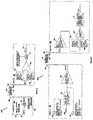
- Figure 4illustrates an implementation of a common wave communication system 400 having a transmitter 401 and a receiver 402.
- the communication system 400may also include a communication link 403 that may be a medium over which a signal can be transmitted between the transmitter and the receiver.
- the mediummay include the atmosphere, space, water, wire, coaxial cable, fiber optics, printed circuit board traces, integrated circuit traces, drilling mud, AC power distribution lines, etc.
- the communication systemmay include at least one data channel 404 that contains a data signal, at least one reference channel 405 that contains a reference signal and one or more other channels 407 that can contain data or reference signals.
- the communication link for the at least one data channel and the communication link for the at least one reference channelmay be the same communication link or may be different communication links.
- the data signalmay be known as a data wave which has an information signal modulated onto a carrier wave using various modulation techniques, such as for example frequency modulation, amplitude modulation, phase modulation, or a combination thereof, etc.
- the reference signalmay be known as a common wave that may be a known frequency signal (that may be fixed or adjustable in a known manner) that acts as a reference wave to the data wave.
- the data wave and the common wavemay be at different frequencies but the different frequencies are close to each other.
- the data wave and the common waveare at different frequencies at any one instant in time
- the data wavemay be at the same frequency as the common wave was at some other instant in time due to the frequency hopping.
- the common wave signalmay be transmitted for a predetermined number of cycles at a particular frequency and then the data wave signal may be transmitted for a predetermined number of cycles (different from the predetermined number of cycles during which the common wave signal is transmitted) at the same frequency or at a different frequency.
- the data wave signal and the common wave signalmay be at the same frequency wherein a series of common wave signals are transmitted and then a series of data wave signals are transmitted (or a series of data wave signals are transmitted and then a series of common wave signals are transmitted) wherein the common wave signals can be used to calibrate the receiver and provide some noise filtering for the data wave signals.
- the one or more data signals 404 and the one or more reference signals 405are simultaneously communicated over the communications link 403 and received by the receiver 402. In other embodiments, the one or more data signals and the one or more reference signals are not simultaneously communicated over the communications link.
- each data signalis compared to a corresponding reference signal in order to extract an information signal from the data signal.
- the common wave systemprovides increased noise immunity because the data signals and the corresponding reference signal will both be affected in a similar manner by noise in the communication link 403 so that the comparison of the data signal to the reference signal in the receiver filters out a portion of the noise, reduces the noise level in the data signal which results in a better signal to noise ratio and thus a higher possible transmission rate as is well known due to Shannon's Law.
- Figure 5illustrates more details of an example of the common wave communication system 400 shown in Figure 4 in which a single data signal channel and a single reference signal channel are shown being communicated over a wireless communication link for illustration purposes.
- the data signal 404 and the reference signal 405are communicated over the communications link 403 between the transmitter 401 and the receiver 402.
- the transmitter 401may have a modulator 503 that modulates an information signal 502 onto a carrier wave 501 (with a specific frequency) to generate the data signal.
- a phase modulator circuitmay be used.
- a common wave signal 405is generated, but is not (in the example shown in Figure 5 ) modulated before it is transmitted.
- the data signal and the common wave signalare then transmitted via one or more antennas 505 over the communication link 403 to the receiver 402.
- the receiver 402may receive the signals from the communication link using one or more antennas 506 wherein the signals received by the antennas 506 that input into a first filter 507 and a second filter 508 wherein the first filter is tuned to the frequency of the carrier wave of the data signal and the second filter is tuned to the frequency of the reference signal.
- the first filterallows the data signal to be output (and filters out other signals) to a first input of a signal comparison device 509 while the second filter allows the reference signals to be output (and filters out other signals) to a second input of the signal comparison device 509.
- the signal comparison devicemay be a differential amplifier that compares the signals at the first and second inputs.
- the signal comparison device 509outputs a signal that is the difference between the data signal and the reference signal, which removes noise introduced in the communication link 403.
- the output of the signal comparison deviceis fed into a demodulator 510 (such as a phase demodulator in the example in Figure 5 ) that also receives a replica of the carrier wave (generated locally in the receiver or extracted from the transmitted signals) in order to generate an information signal 511 that corresponds to the information signal 502 input to the transmitter 401.
- a demodulator 510such as a phase demodulator in the example in Figure 5
- the output of the differential amplifiercan then be analyzed to identify the data (demodulated). While this signal will be significantly different than normal wireless signals to be demodulated, it can be analyzed with well-known techniques using standard circuitry or digital signal processors (DSP).
- DSPdigital signal processors
- Figure 6illustrates an example of an implementation of the common wave communication system shown in Figure 4 .
- the transmitter 401may further comprise a carrier wave generator 601, such as for example a voltage controller oscillator, that generates the carrier wave such as a carrier wave at 910.546 MHz and a reference wave generator 602, such as for example a voltage controller oscillator, that generates the reference wave such as a reference wave at 925.000 MHz.
- the modulator 503may be a phase shifter circuit that shifts the carrier wave phase based on the information signal 502.
- the data signal and the reference waveare input into a signal amplifier 603, such as a radio frequency amplifier, that boosts the strength of both signals before they are radiated by the one or more antennas 505.
- the receiver 402 in this implementationmay further include an amplifier 604, such as a low noise amplifier, that boosts the signal strength of the received signals (both the data signal and the reference signal), which are then fed into the filters 507, 508.
- the demodulator 510may be a circuit (such as a thresholding circuit) that compares the incoming information signal (output from the signal comparison device 509) to an expected signal for a "1” or a "0” and outputs the recovered information signal.
- Figure 7shows the expected signals for a "1” and a "0” for one embodiment in which the "1" starts positive 90 degrees out of phase with the data wave and the "0" starts negative 90 degrees out of phase with the data wave.
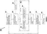
- Figure 8illustrates an example of a method 800 for common wave communication that may be carried out by the transmitter and receiver shown in Figures 4-6 above.
- the systemselects a relationship between the data signal and the reference signal (801) which may be communicated to the receiver in some fashion (e.g., the relationship may be preconfigured or set during each communication session).
- the relation shipmay be specific differences in amplitudes, frequencies, phases and/or polarities at specific points in time.
- the systemcan have a default setting (set at both the transmitter and receiver) and then can adjust the relationship as needed by communicating with each other.
- An example of the default relationshipmay be a typical amplitude, frequency and/or phase modulation and the changing of the relationship during the communications may be done to provide frequency hopping and/or adjusting signal strength.
- the transmittermay create a reference signal and a data signal (802) based on an information signal (803).
- the data signalis communicated over a data signal channel (804) and the reference signal is communicated over a reference signal channel (805) over one or more communications link(s) 403.
- the receiverthen receives the transmitter signals (806) and then uses the relationship information to extract the information signal from the data signal in the data channel (807) so that the information signal is outputted (808).
- Figure 9illustrates an example of a method for resetting a data signal of the common wave communication system.
- the transmittermay periodically reset the data signal to bring it back into phase with the data signal as shown in Figure 9 .
- the data wavemay be reset every 4 signal periods (such as shown in Figure 9 ).
- the resetting of the data signalmay also be used for amplitude modulation embodiments, frequency modulation embodiments and other modulation embodiments.
- the resetting of the data signalmay also be used with systems that do not simultaneously transmit a data signal and a reference signal.
- the common wave systemmay transmit the common wave at a fixed frequency and the signal is essentially unmodulated and the data channels with the data signals are at different frequencies and the amplitude of the data channel signals have a known relationship to the common wave signals.
- the common wave signal amplitudemay be significantly higher than the data signals, such as 0-20 dB.
- a very narrow band pass filterBPF detects the common wave signal.
- the significantly higher amplitude common wave signalestablishes, at the receiver, a strong reference signal for evaluating the frequency, phase, amplitude and/or time of the data signals.
- the strong reference signalmay be used by hardware, software, a digital signal processor (DSP), etc. to differentiate the data signal from noise and decoding/recovering the data signals.
- the common wave signalmay be transmitted at an effective radiated power (ERP) of 100 watts and there may be eight data channels each transmitting at an ERP of 50 W to 8 different receivers.
- the receivermay have a band pass filter with a bandwidth of 100 kHz so that the receiver will be receiving a strong signal that is being sampled over a 10 microsecond period. It is well known that a 100 W signal is better able to penetrate walls and weather and deal with noise, multipath and travel speeds than a 50 W signal. Therefore, each of the eight receivers will receive a strong common wave signal which will be used as a reference for evaluation the specific signal that is of interest to the specific receiver.
- the above higher power common wave signalmay be broadcast to a large number of receivers that can each utilize the common wave signal so that the ratio of the common wave signal to the number of data wave signals may be 1 to 8 (the above example), 1 to 100, 1 to 1000 or 1 to 1,000,000.
- the ratio of the common wave signal to the number of data wave signalsmay be 1 to 8 (the above example), 1 to 100, 1 to 1000 or 1 to 1,000,000.
- the advantage of more data channels using the same common wave signalis that the common wave signal takes up a smaller percentage of the total allowable ERP.
- multiple mobile phone service providers using the same cell towercould use the same common wave signal thereby allowing all of them to increase the ERP to each data channel.
- Figures 10 and 11illustrate an example of a method for minimizing effective bandwidth of a communication system.
- the method illustrated in Figures 10-11may be used with conventional communication systems as well as the common wave communication system.
- the frequency band that will be transmittedis from 990 MHz to 1.010 GHz which causes interference problems with 995 MHz if it needs to be used as a transmission channel.
- the resulting increase in bandwidthis one of many factors that limit the total amount of data that can be transmitted in a given frequency band.
- the communication systemmay use a carrier wave that is phase shifted 180 degrees at predetermined times as shown in Figure 10 . For simplicity, the information signal that is modulated onto the carrier wave is not shown.
- this phase shiftingmakes the average power at the carrier frequency and the nearby channels, e.g., 995 MHz, zero. This allows 995 MHz to be used as a communications channel using the common wave system or conventional technologies and be unaffected by the 1 GHz channel.
- the receiverif the transmission signal is phase shifted every 10 cycles, the receiver must also be "phase shifted" to be able to handle the incoming signal. If adjacent channels also use this phase shifting approach, the timing for each channel's phase shifting can be offset from the other channels. This will enable more channels to be crammed into the same frequency band without interchannel interference.
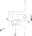
- FIG. 12shows an embodiment of an alternating phase signal filter 1200 which effectively reaches resonance for a signal with an alternating phase.
- a switch 1201alternates positions based on the switch control input. The timing of the position switch is such that the conventional bandpass filter or resonant circuit 1202 always has the same phase input to it. This allows the circuit to achieve resonance and thus pass a strong signal at the desired frequency and phase. Also, this will cause destructive interference for frequencies and phases that are not desired.
- This same type alternating phase signal filter 1200will work well with signals that have been reset as shown in Figure 9 .
- the carrier waveis phase shifted 180 degrees but it can be appreciated that other combinations of phase shifting can achieve the similar results and the system is not limited to the 180 degree phase shift shown in Figure 10 .
- 10 carrier waves at 0 degrees, 10 carrier waves at 120 degrees and 10 carrier waves at -120 degreeswill have a lower average power at the carrier frequency than 30 waves at 0 degrees.
- combinations of different phases, amplitudes and frequenciescan have similar effects and are within the scope of this disclosure.
- Figures 13 and 14illustrate an example of a method for neutralizing sidebands of a communication system.
- the method illustrated in Figures 13-14may be used with conventional communication systems as well as the common wave communication system.
- a wireless signalis changed (amplitude, frequency and/or phase) the bandwidth is increased and sidebands are created.
- the sidebandsare a necessary part of wireless communication in many protocols, e.g., "single sideband.” In many circumstances though, sidebands are an undesirable byproduct of the signal modulation.
- a 950 MHz signal with a specific predetermined amplitude and phaseare used to neutralize that sideband and Figure 13 shows that the resultant signal where the 950 MHz sideband is neutralized.
- the injected signalneeds to be the same amplitude and 180 degrees phase shifted from the sideband to be neutralized.
- the carrier wavehas an amplitude of 1 volt (see Figure 10 ) and the injected 950 MHz signal has an amplitude of 0.6525 volt.
- the injected signalstarts out of phase with the carrier wave 90 degrees.
- additional signalscan be similarly injected to eliminate other side bands.
- the injection of a signal into the transmission linecan be used to eliminate sidebands created from all sources of sidebands as long as the amplitude, frequency and phase of the sideband is known in advance. These values can be determined from previous transmissions in a laboratory environment and then be used in a field setting. Even in the case of sidebands created from data modulation, an appropriate sideband neutralizing signal can be injected into the transmission line. The specifics of that neutralizing signal will be different depending on the value of the data.
- the original carrier waveis recovered using known techniques.
- those injected neutralizing signalsare removed to recover the original carrier wave.
- transmission lineis defined as any path used to transfer the signal energy from one location to another. This includes but is not limited to: conductors in the transmitter, waveguides, lines connecting the transmitter to the one or more antennae, amplifiers or communications links, including wireless communications links.
- sideband mitigationsideband mitigation
- simulationsare used to illustrate the neutralization of sidebands.
- the example presented belowillustrates how the neutralization of sidebands can substantially increase the spectral efficiency of wireless communication.
- well known signalswill be shown as a starting point and then signals utilizing the described sideband mitigation will be shown for comparison.
- a carrier wave of 1 GHzis used although the disclosed sideband mitigation can be used with any frequency and thus is not limited to any particular frequency.
- This exemplary frequencyis used because it is in close proximity to common frequency bands such as cellular phones (800, 900, 1800, 2100 MHz), WiFi (2.4 GHz) and WiMax (2.3, 2.5 and 3.5 GHz).
- the simulation software usedis LTspice/SwitcherCAD III Version 2.24i produced by Linear Technology Corporation.
- a circuit that can create the 1 GHz carrier wave for this exampleis shown in Figure 15 .
- the voltage sourcegenerates a sine wave with a 1.414 V amplitude and 1 GHz frequency. Simulating this circuit in the time domain provides voltage vs. time oscilloscope output as shown in Figure 16 . Performing a well known
- FFTFast Fourier Transform
- the power for the carrier wave shown aboveis 20mW which is below the maximum levels for those bands and 1 GHz.
- a data signalis generated by V2 and output to TP_Data in Figure 19 .
- the following data for the exampleis arbitrarily selected: 10110011 10001111 00001111 10000011 11110000 00111111 10000000 11111111 00000000 11111111 10000000 00111111 11110000 00000011 11111111 10000000
- the data rateis 125 Mbps which is a period of 8 ns.
- the first 124 ns of the signalis seen in Figure 20 .
- the Phase_Modulator_90_degree shown in Figure 19modulates the carrier wave with the data wave wherein a data bit "1" is phase shifted 90° and a data bit "0" is phase shifted 0°.
- Figure 21shows the first 36ns of the modulated signal.
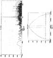
- Figure 22shows the FFT of the modulated signal that has significant sidebands. As expected, the lobes do not fit within the mask because the data rate is too high. As seen, the 20dB bandwidth is 22 MHz as shown in Figure 22 .
- Spectral EfficiencyData Rate / Bandwidth
- any attempt to use a bandpass filter (a typical solution) to improve the spectral efficiency of the signal of Figure 21will not be useful because the bandpass filter will filter out the data.
- the spectral efficiencycan be improved using known techniques which include the use of: reducing the delta phase shift below 90° (e.g., 11.5°), amplitude modulation, and others.
- These known techniqueswork and are used regularly but have limitations due to real world noise and sensitivity of the hardware. For example, reducing the delta phase shift 11.5° will make the receiver more susceptible to phase noise (jitter) and approaches the limits of the resolution of phase detector.
- the typical solutionshave limitations and/or do not provide sufficient results.
- the sideband mitigation technique disclosed hereinimproves over these known techniques and in fact can be used with these known techniques to reduce sidebands and increase spectral efficiency.
- each data bitis phase shift 0 for half the data period and phase shift 180 for the other half. If the data bit is a 1, it is phase 0 for the first half and phase 180 for the second half. If the data bit is a 0, it is phase 180 for the first half and phase 0 for the second half as shown in Figure 24 .
- " ⁇ "shown in Figure 23 is an operand that "Convert(s) the expressions to either side to Boolean, then XORs (exclusive ors) the result.
- the modulation of the sideband mitigation techniquecauses each data bit to cancel itself out on the FFT which results in the 1 GHz lobe being eliminated as seen in Figure 25 , but the other lobes in Figure 22 are worse than before.
- Zooming in on 867 MHz in Figure 25 and adding phasegives Figure 26 in which the lobe is centered at 867 MHz, the peak is at -11.7 dB and the phase is -24° (and 1GHz is at -7°.)
- To mitigate the 867 MHz lobewe add a 867 MHz, 0.368 V amplitude, 245° phase sine wave, V(TP_FN2) to the signal. The results are TP_FN2 and shown in Figures 27 and 28 .
- Figure 28shows residual lobes remain from the first mitigation attempt.
- To mitigate the 868 MHz lobeadd a 868.6 MHz lobe w/ 0.200 amplitude and 250° phase. These results are shown in Figure 29 .
- These stepscan be repeated for elimination of all the lobes above the -20 dB mask thereby enabling a 125 Mbps data rate to fit within a 250 kHz bandwidth FCC allocation.
- the appropriate characteristics of the neutralizing signalcan be determined by a formula in which the data to be transmitted is input into the formula or by a lookup table in which the data to be transmitted is used.
- phase filteringis useful in the receiver for demodulation
- Phase modulationis particularly valuable for incoming signals that have noise and interference from nearby data channels.
- an assumption of the valuee.g., a 1 or a 0
- a signal equivalent to that assumptionis injected into the incoming signal. If the assumption of the data value is correct, constructive interference between the incoming signal and the injected signal will provide constructive interference and verify the assumption. If the assumption of the data value is wrong, destructive interference will show the assumption to be wrong.
- the difference in the output signal between a correct and incorrect assumptionwill be quite substantial. This is because the correct assumption on the injected signal and the incoming data portion of the data signal will increase the output signal's amplitude every wave.
- the incoming signalmay be split 1505 into 2 circuits wherein one circuit 1501 assumes that the data is a "1" and the other circuit 1502 assumes the data is a "0".
- the signal generators 1503 and 1504generate signals equivalent to their respective assumption of 1 and 0 respectively.
- Resistors 1506are used to add the input signal to the simulated signals. If all four of the resistors shown are the same value, the signals will all be added evenly. If gain is required for specific signals, the resistors of different values can be used.
- the output from these two circuitsmay be run through a signal comparison device 1507 and the output of the signal comparison device provides a signal with a strong indication of which assumption ("0" or "1") is the correct assumption. While this output signal will be significantly different than normal wireless signals to be demodulated, it can be analyzed with well known techniques using standard circuitry or digital signal processors (DSP).
- DSPdigital signal processors
Landscapes
- Engineering & Computer Science (AREA)
- Computer Networks & Wireless Communication (AREA)
- Signal Processing (AREA)
- Power Engineering (AREA)
- Physics & Mathematics (AREA)
- Spectroscopy & Molecular Physics (AREA)
- Transmitters (AREA)
- Digital Transmission Methods That Use Modulated Carrier Waves (AREA)
- Transceivers (AREA)
- Circuits Of Receivers In General (AREA)
- Noise Elimination (AREA)
- Telephone Function (AREA)
Description
- A wired or wireless communication system and method are provided.
- Various wired and wireless communication systems are well known. For example, as shown in
Figures 1 and 2 , two different conventional communication systems are known. As shown inFigure 1 , one example of a conventional wired communication system has a transmitter and receiver wherein a data signal is communicated over a first wired communications link and a second data signal (which is an inverted form of the data signal) is communicated over a second wired communications link. In the system shown inFigure 1 , the two wired communications links are nearby each other. The receiver may receive these two data signals and then take the difference between the two data signals in order to extract the data from the data signal. This conventional communication system is known as a differential signal system that allows lower voltages to be used since only the difference between the two signals is needed, allows higher data transmission speeds and increases noise immunity since any noise would affect both the communication links and the noise would be filtered out when the difference between the two data signals is determined. The system shown inFigure 1 may be used, for example, on a printed circuit board in which each wired communication link is a trace on the printed circuit board. - An example of how the system in
Figure 1 works on copper wires is that the two adjacent wires each have a signal in which one is the inverse of the other. For example, if a "digital 1" is to be transmitted with 1 volt levels, Line A will be at 1 volt and Line B will be at 0 volt (i.e., the inverse) while a "digital 0" is transmitted with Line A at 0 volts and Line B at 1 volt. As the wires run from the transmitter to the receiver, the wires might both pickup noise which will cause the voltage levels in the lines to be raised or lower in addition to causing spikes which can appear to be data. If the 2 wires are in very close physical proximity to each other, the noise will be identical in both wires. At the receiver end, the 2 lines will be connected to a differential amplifier circuit. This differential amplifier circuit will "subtract out" the noise. Figure 2 illustrates an example of another conventional communication system that may be a wireless communication system. In this communication system, a transmitter may generate and communicate a plurality of data signals over a communication link and then the receiver extracts data from each data signal independently, but there is no relationship between the data signals that aids in the extraction of the data from the data signals. The system shown inFigure 2 may be used for a typical mobile phone system such as a time division multiplex or a code division multiplex communication system.Figure 3 illustrates a wireless communications system that uses a pilot signal wherein the pilot signal is modulated with the carrier wave and data signal to generate a single output signal that is then sent over a communications link to a receiver. The receiver then uses the pilot signal (embedded in the output signal) to decode the data signal. In this conventional system with a pilot signal, only a single signal is sent over the communications link.- None of these conventional communication systems use a data signal and a reference signal (transmitted over the same communications link but on different channels) and thus it is desirable to provide a common wave system and method and it is to this end that the system and method are directed.
- A noise suppression technique for radio circuits is known from
US 3084329 A . Said technique makes use of the redundancy of information conveyed by the two sidebands. The basic technique of the invention involves the inversion of one of the sidebands so that sidebands of opposite polarity are obtained. WO 2007/067379 A2 discloses control for communication systems transmitting and receiving signals with substantially no sidebands. Modulation of signals includes substantially no side bands in a frequency domain. Circuitry in a communication system of same includes a control signal derived from a carrier, or vice versa, to modulate an input signal. A preferred carrier embodies a sine wave while the preferred control signal is a square wave. A frequency of the control signal includes once or twice multiple integers of the frequency of the sine wave, particularly when impressing data on the carrier per every full or half wave cycle of the sine wave, respectively. An input signal adjusted in frequency to match the carrier frequency is used as an input to a gain adjustable module to adjust gain thereof. The carrier is another input to the module and the output of the module is the signal having substantially no sidebands. Transmitters, receivers, systems and communication medium are also disclosed.US 2003/232607 A1 proposes a wireless transmitter composed of at least one modulator, which comprises a digital part and an analog part. The digital part comprises elements for generating the envelope of the signals to be transmitted and elements for generating the phase of the signals to be transmitted.- It is desirable to provide systems and methods for minimizing effective bandwidth and neutralizing sidebands (sideband mitigation) that enable substantial increases in data transmission speed and spectral efficiency and it is to this end that the system and method are also directed.
- The present invention provides a solution according to the subject matter of the independent claims.
Figures 1 and 2 illustrate conventional communication systems;Figure 3 illustrates a conventional pilot signal communication system;Figure 4 illustrates an implementation of a common wave communication system having a transmitter and receiver;Figure 5 illustrates more details of an example of the common wave communication system shown inFigure 4 ;Figure 6 illustrates an example of an implementation of the common wave communication system shown inFigure 4 ;Figure 7 illustrates an example of expected signals for a demodulator circuit in a common wave communications system receiver to compare to the input signal;Figure 8 illustrates an example of a method for common wave communication;Figure 9 illustrates an example of a method for resetting a data signal of the common wave communication system;Figures 10 and 11 illustrate an example of a method for minimizing effective bandwidth of a communication system;Figure 12 illustrates an example of a filter for use with signals that have alternating phases;Figures 13 and 14 illustrate an example of a method for neutralizing sidebands of a communication system;Figure 15 illustrates an example of a circuit for generating 1 GHz carrier wave with a 1.414V amplitude & 0° phase;Figure 16 illustrates an example of a time domain for the 1 GHz carrier wave unmodulated;Figure 17 illustrates an example of a FFT of the 1 GHz unmodulated signal for 1000ns;Figure 18 illustrates an example of a FFT for 1 GHz unmodulated signal for 1000ns sample with 250kHz -20dB mask;Figure 19 illustrates an example of a circuit with data signal generated by V2 and modulation done by Phase_Modulator_90_deg;Figure 20 illustrates an example of a data signal for the first 124ns. Data bit period is 8ns;Figure 21 illustrates an example of a modulated signal.Data bit 1 is phase 90°.Data bit 0 isphase 0°. 34 ns shown;Figure 22 illustrates an example of an FFT of the 125 Mbps, 90° phase shift, modulated signal;Figure 23 illustrates an example of an implementation of a first step in Sideband Mitigation circuitry;Figure 24 illustrates an example of a modulated signal hasdata bit 1 start withphase 0 anddata bit 0 start withphase 180;Figure 25 illustrates an example of an FFT with 1 GHz lobe removed. Sidebands are worse;Figure 26 illustrates the 867 MHz and 884 MHz lobes shown with phase;Figure 27 illustrates an example of an implementation of a Sideband Mitigating signal added to reduce a 867 MHz lobe;Figure 28 illustrates an example of a 867 MHz lobe minimized but residual lobes remain;Figure 29 illustrates an example of an implementation of a 868 MHz residual lobe that has been mitigated;Figure 30 illustrates an example of an implementation of a signal with all the sidebands below 1 GHz mitigated;Figure 31 illustrates an example of an implementation of an FFT with sidebands below 1GHz mitigated with Sideband Mitigation signals shown in Table 1; andFigure 32 illustrates an example of a circuit for phase filtering.- The system and method are particularly applicable to a wireless communication system with a single communications link using a discrete hardware circuit based transmitter and receiver as described below and it is in this context that the system and method will be described. It will be appreciated, however, that the system and method has greater utility since the system and method may be used with wired (for example, a fiber optic, wires, a printed circuit board (PCB) trace, etc.) or wireless communication systems (for example, cellular phone systems, mobile device wireless systems, etc.), may be implemented as a transmitter or a receiver only, and/or may be implemented in software (soft transmitter and/or receiver), hardware (as shown below or other implementations) or a combination of software and hardware (for example a digital signal processor with firmware or other implementations).
- In the context of this disclosure, "mobile device" may include any mobile wireless communications device including but not limited to: a cellular phone, Personal Communications Service PCS, smartphone (e.g., iPhone, BlackBerry, etc.), wireless internet cards or circuits for computers, wireless local and wide area network (e.g., WiFi, WiMax, etc.) cards or circuits, satellite phones, GPS tracking devices, etc. The device using the common wave system and method is mobile device regardless of the type of data the device is transmitting or receiving. For example, the data being transmitted or received may include any type of information including but not limited to voice, data files, video, broadcasts, music, telemetry, radio, etc.
Figure 4 illustrates an implementation of a commonwave communication system 400 having atransmitter 401 and areceiver 402. Thecommunication system 400 may also include acommunication link 403 that may be a medium over which a signal can be transmitted between the transmitter and the receiver. The medium may include the atmosphere, space, water, wire, coaxial cable, fiber optics, printed circuit board traces, integrated circuit traces, drilling mud, AC power distribution lines, etc. In the communication system, there may be a plurality ofchannels 406 in thecommunication link 403. The communication system may include at least onedata channel 404 that contains a data signal, at least onereference channel 405 that contains a reference signal and one or moreother channels 407 that can contain data or reference signals. The communication link for the at least one data channel and the communication link for the at least one reference channel may be the same communication link or may be different communication links.- In the common wave system, the data signal may be known as a data wave which has an information signal modulated onto a carrier wave using various modulation techniques, such as for example frequency modulation, amplitude modulation, phase modulation, or a combination thereof, etc. The reference signal may be known as a common wave that may be a known frequency signal (that may be fixed or adjustable in a known manner) that acts as a reference wave to the data wave. In one embodiment, the data wave and the common wave may be at different frequencies but the different frequencies are close to each other. In one embodiment, such as code division multiple access (CDMA) mobile phone system that employs frequency hopping, although the data wave and the common wave are at different frequencies at any one instant in time, the data wave may be at the same frequency as the common wave was at some other instant in time due to the frequency hopping. In another embodiment, the common wave signal may be transmitted for a predetermined number of cycles at a particular frequency and then the data wave signal may be transmitted for a predetermined number of cycles (different from the predetermined number of cycles during which the common wave signal is transmitted) at the same frequency or at a different frequency. In another embodiment, the data wave signal and the common wave signal may be at the same frequency wherein a series of common wave signals are transmitted and then a series of data wave signals are transmitted (or a series of data wave signals are transmitted and then a series of common wave signals are transmitted) wherein the common wave signals can be used to calibrate the receiver and provide some noise filtering for the data wave signals.
- In one embodiment of the common wave system, the one or more data signals 404 and the one or
more reference signals 405 are simultaneously communicated over the communications link 403 and received by thereceiver 402. In other embodiments, the one or more data signals and the one or more reference signals are not simultaneously communicated over the communications link. When the one or more data signals and the one or more reference signals are received by thereceiver 402, each data signal is compared to a corresponding reference signal in order to extract an information signal from the data signal. The common wave system provides increased noise immunity because the data signals and the corresponding reference signal will both be affected in a similar manner by noise in thecommunication link 403 so that the comparison of the data signal to the reference signal in the receiver filters out a portion of the noise, reduces the noise level in the data signal which results in a better signal to noise ratio and thus a higher possible transmission rate as is well known due to Shannon's Law. Figure 5 illustrates more details of an example of the commonwave communication system 400 shown inFigure 4 in which a single data signal channel and a single reference signal channel are shown being communicated over a wireless communication link for illustration purposes. As above, the data signal 404 and thereference signal 405 are communicated over the communications link 403 between thetransmitter 401 and thereceiver 402. Thetransmitter 401 may have amodulator 503 that modulates an information signal 502 onto a carrier wave 501 (with a specific frequency) to generate the data signal. In one embodiment, a phase modulator circuit may be used. Acommon wave signal 405 is generated, but is not (in the example shown inFigure 5 ) modulated before it is transmitted. The data signal and the common wave signal are then transmitted via one ormore antennas 505 over thecommunication link 403 to thereceiver 402.- The
receiver 402 may receive the signals from the communication link using one ormore antennas 506 wherein the signals received by theantennas 506 that input into a first filter 507 and a second filter 508 wherein the first filter is tuned to the frequency of the carrier wave of the data signal and the second filter is tuned to the frequency of the reference signal. Thus, the first filter allows the data signal to be output (and filters out other signals) to a first input of a signal comparison device 509 while the second filter allows the reference signals to be output (and filters out other signals) to a second input of the signal comparison device 509. In one embodiment, the signal comparison device may be a differential amplifier that compares the signals at the first and second inputs. Thus, the signal comparison device 509 outputs a signal that is the difference between the data signal and the reference signal, which removes noise introduced in thecommunication link 403. The output of the signal comparison device is fed into a demodulator 510 (such as a phase demodulator in the example inFigure 5 ) that also receives a replica of the carrier wave (generated locally in the receiver or extracted from the transmitted signals) in order to generate an information signal 511 that corresponds to the information signal 502 input to thetransmitter 401. In one embodiment using a differential amplifier, the output of the differential amplifier can then be analyzed to identify the data (demodulated). While this signal will be significantly different than normal wireless signals to be demodulated, it can be analyzed with well-known techniques using standard circuitry or digital signal processors (DSP). Figure 6 illustrates an example of an implementation of the common wave communication system shown inFigure 4 . In this implementation, thetransmitter 401 may further comprise a carrier wave generator 601, such as for example a voltage controller oscillator, that generates the carrier wave such as a carrier wave at 910.546 MHz and a reference wave generator 602, such as for example a voltage controller oscillator, that generates the reference wave such as a reference wave at 925.000 MHz. In this implementation, themodulator 503 may be a phase shifter circuit that shifts the carrier wave phase based on the information signal 502. In this implementation, the data signal and the reference wave are input into a signal amplifier 603, such as a radio frequency amplifier, that boosts the strength of both signals before they are radiated by the one ormore antennas 505.- The
receiver 402 in this implementation may further include anamplifier 604, such as a low noise amplifier, that boosts the signal strength of the received signals (both the data signal and the reference signal), which are then fed into the filters 507, 508. In this implementation, thedemodulator 510 may be a circuit (such as a thresholding circuit) that compares the incoming information signal (output from the signal comparison device 509) to an expected signal for a "1" or a "0" and outputs the recovered information signal.Figure 7 shows the expected signals for a "1" and a "0" for one embodiment in which the "1" starts positive 90 degrees out of phase with the data wave and the "0" starts negative 90 degrees out of phase with the data wave. Figure 8 illustrates an example of amethod 800 for common wave communication that may be carried out by the transmitter and receiver shown inFigures 4-6 above. At the transmitter, the system selects a relationship between the data signal and the reference signal (801) which may be communicated to the receiver in some fashion (e.g., the relationship may be preconfigured or set during each communication session). The relation ship may be specific differences in amplitudes, frequencies, phases and/or polarities at specific points in time. In one embodiment, the system can have a default setting (set at both the transmitter and receiver) and then can adjust the relationship as needed by communicating with each other. An example of the default relationship may be a typical amplitude, frequency and/or phase modulation and the changing of the relationship during the communications may be done to provide frequency hopping and/or adjusting signal strength. Once the relationship is determined, the transmitter may create a reference signal and a data signal (802) based on an information signal (803). Once the signals are generated in the transmitter, the data signal is communicated over a data signal channel (804) and the reference signal is communicated over a reference signal channel (805) over one or more communications link(s) 403. The receiver then receives the transmitter signals (806) and then uses the relationship information to extract the information signal from the data signal in the data channel (807) so that the information signal is outputted (808).Figure 9 illustrates an example of a method for resetting a data signal of the common wave communication system. When the reference signal and the data signal are simultaneously transmitted, the two signals become superimposed which may cause significant destructive interference for much of the time (about 50% of the time) which is common to many wireless systems. To overcome this superimposition issue, in one embodiment of the common wave communication system using phase modulation, the transmitter may periodically reset the data signal to bring it back into phase with the data signal as shown inFigure 9 . In one embodiment, the data wave may be reset every 4 signal periods (such as shown inFigure 9 ). In addition to the phase modulation embodiment, the resetting of the data signal may also be used for amplitude modulation embodiments, frequency modulation embodiments and other modulation embodiments. In addition to the common wave communication system with the data signal and reference signal simultaneously transmitted, the resetting of the data signal may also be used with systems that do not simultaneously transmit a data signal and a reference signal.- As described above, the common wave system may transmit the common wave at a fixed frequency and the signal is essentially unmodulated and the data channels with the data signals are at different frequencies and the amplitude of the data channel signals have a known relationship to the common wave signals. In one embodiment, the common wave signal amplitude may be significantly higher than the data signals, such as 0-20 dB. Then, at the receiver, a very narrow band pass filter (BPF) detects the common wave signal.
- The significantly higher amplitude common wave signal establishes, at the receiver, a strong reference signal for evaluating the frequency, phase, amplitude and/or time of the data signals. The strong reference signal may be used by hardware, software, a digital signal processor (DSP), etc. to differentiate the data signal from noise and decoding/recovering the data signals.
- As an example, the common wave signal may be transmitted at an effective radiated power (ERP) of 100 watts and there may be eight data channels each transmitting at an ERP of 50 W to 8 different receivers. For the common wave signal, the receiver may have a band pass filter with a bandwidth of 100 kHz so that the receiver will be receiving a strong signal that is being sampled over a 10 microsecond period. It is well known that a 100 W signal is better able to penetrate walls and weather and deal with noise, multipath and travel speeds than a 50 W signal. Therefore, each of the eight receivers will receive a strong common wave signal which will be used as a reference for evaluation the specific signal that is of interest to the specific receiver.
- In most actual implementations of communication systems, there are limits on the amount of power each transmitter is allowed to transmit. For example, in general in the United States, mobile phone tower transmitters are only allowed to transmit 500 W ERP so that one cannot design an implementation of a communication system with eight 100W data signals because the transmitter would exceed the maximum power allowed. However, an implementation that has a powerful common wave signal and a plurality of data wave signals at lesser power allow the communication system to meet the transmission maximum power levels while allowing the data signals to be more accurately decoded/recovered due to the stronger power common wave signal. The above higher power common wave signal may be broadcast to a large number of receivers that can each utilize the common wave signal so that the ratio of the common wave signal to the number of data wave signals may be 1 to 8 (the above example), 1 to 100, 1 to 1000 or 1 to 1,000,000. In fact, there is no limit to the number of data channels that can use a single common wave signal. The advantage of more data channels using the same common wave signal is that the common wave signal takes up a smaller percentage of the total allowable ERP. In one embodiment, multiple mobile phone service providers using the same cell tower could use the same common wave signal thereby allowing all of them to increase the ERP to each data channel.
Figures 10 and 11 illustrate an example of a method for minimizing effective bandwidth of a communication system. The method illustrated inFigures 10-11 may be used with conventional communication systems as well as the common wave communication system.- In an exemplary communication system, if a carrier frequency is 1 GHz, and digital data is modulated via AM, FM or PM at 10 MHz, the frequency band that will be transmitted is from 990 MHz to 1.010 GHz which causes interference problems with 995 MHz if it needs to be used as a transmission channel. The resulting increase in bandwidth is one of many factors that limit the total amount of data that can be transmitted in a given frequency band. To overcome this interference at 995 MHz and minimize the bandwidth of the carrier wave, the communication system may use a carrier wave that is phase shifted 180 degrees at predetermined times as shown in
Figure 10 . For simplicity, the information signal that is modulated onto the carrier wave is not shown. As shown inFigure 11 , this phase shifting makes the average power at the carrier frequency and the nearby channels, e.g., 995 MHz, zero. This allows 995 MHz to be used as a communications channel using the common wave system or conventional technologies and be unaffected by the 1 GHz channel. - In one embodiment, if the transmission signal is phase shifted every 10 cycles, the receiver must also be "phase shifted" to be able to handle the incoming signal. If adjacent channels also use this phase shifting approach, the timing for each channel's phase shifting can be offset from the other channels. This will enable more channels to be crammed into the same frequency band without interchannel interference.
- In traditional filters for transmitters or receivers, alternating the phase of a signal as shown in
Figure 10 can prevent the circuit from resonating effectively and hence the circuit will output a weak signal.Figure 12 shows an embodiment of an alternatingphase signal filter 1200 which effectively reaches resonance for a signal with an alternating phase. Aswitch 1201 alternates positions based on the switch control input. The timing of the position switch is such that the conventional bandpass filter orresonant circuit 1202 always has the same phase input to it. This allows the circuit to achieve resonance and thus pass a strong signal at the desired frequency and phase. Also, this will cause destructive interference for frequencies and phases that are not desired. This same type alternatingphase signal filter 1200 will work well with signals that have been reset as shown inFigure 9 . - In the embodiment shown in
Figure 10 , the carrier wave is phase shifted 180 degrees but it can be appreciated that other combinations of phase shifting can achieve the similar results and the system is not limited to the 180 degree phase shift shown inFigure 10 . For example: 10 carrier waves at 0 degrees, 10 carrier waves at 120 degrees and 10 carrier waves at -120 degrees will have a lower average power at the carrier frequency than 30 waves at 0 degrees. Also, combinations of different phases, amplitudes and frequencies can have similar effects and are within the scope of this disclosure. Figures 13 and 14 illustrate an example of a method for neutralizing sidebands of a communication system. The method illustrated inFigures 13-14 may be used with conventional communication systems as well as the common wave communication system. When a wireless signal is changed (amplitude, frequency and/or phase) the bandwidth is increased and sidebands are created. The sidebands are a necessary part of wireless communication in many protocols, e.g., "single sideband." In many circumstances though, sidebands are an undesirable byproduct of the signal modulation.- As shown in
Figure 11 , significant sidebands are seen which are generated by the phase shifting of the carrier signal. These are undesirable because they will be radiated and cause interference with other channels at those frequencies. The traditional method of eliminating sidebands is the use of low pass, high pass or bandpass filters. These traditional filters are undesirable in a situation where high speed data signals are involved because the filters degrade the high speed signals. In the neutralizing sideband method that may be used with the common wave system, a "neutralizing signal" may be injected into the transmission line along with the carrier signal. As shown inFigure 13 , to neutralize the 950 MHz sideband, a 950 MHz signal with a specific predetermined amplitude and phase are used to neutralize that sideband andFigure 13 shows that the resultant signal where the 950 MHz sideband is neutralized. For example, the injected signal needs to be the same amplitude and 180 degrees phase shifted from the sideband to be neutralized. In the example shown inFigure 13 , the carrier wave has an amplitude of 1 volt (seeFigure 10 ) and the injected 950 MHz signal has an amplitude of 0.6525 volt. The injected signal starts out of phase with the carrier wave 90 degrees. In addition, additional signals can be similarly injected to eliminate other side bands. - The injection of a signal into the transmission line can be used to eliminate sidebands created from all sources of sidebands as long as the amplitude, frequency and phase of the sideband is known in advance. These values can be determined from previous transmissions in a laboratory environment and then be used in a field setting. Even in the case of sidebands created from data modulation, an appropriate sideband neutralizing signal can be injected into the transmission line. The specifics of that neutralizing signal will be different depending on the value of the data.
- At the receiver end of the transmission system, the original carrier wave is recovered using known techniques. In the case of the injected neutralizing signals, those injected neutralizing signals are removed to recover the original carrier wave.
- In the context of the disclosure, "transmission line" is defined as any path used to transfer the signal energy from one location to another. This includes but is not limited to: conductors in the transmitter, waveguides, lines connecting the transmitter to the one or more antennae, amplifiers or communications links, including wireless communications links.
- Now, a detailed example of the above neutralization of sidebands (sideband mitigation) is described in which simulations are used to illustrate the neutralization of sidebands. The example presented below illustrates how the neutralization of sidebands can substantially increase the spectral efficiency of wireless communication. In the example, well known signals will be shown as a starting point and then signals utilizing the described sideband mitigation will be shown for comparison. For purposes of the example, a carrier wave of 1 GHz is used although the disclosed sideband mitigation can be used with any frequency and thus is not limited to any particular frequency. This exemplary frequency is used because it is in close proximity to common frequency bands such as cellular phones (800, 900, 1800, 2100 MHz), WiFi (2.4 GHz) and WiMax (2.3, 2.5 and 3.5 GHz). For purposes of the example, the simulation software used is LTspice/SwitcherCAD III Version 2.24i produced by Linear Technology Corporation.
- A circuit that can create the 1 GHz carrier wave for this example is shown in
Figure 15 . The voltage source generates a sine wave with a 1.414 V amplitude and 1 GHz frequency. Simulating this circuit in the time domain provides voltage vs. time oscilloscope output as shown inFigure 16 . Performing a well known - FFT (Fast Fourier Transform) simulation on the signal voltage results in
Figure 17 . For purposes of this example, all FFT operations are performed for a 1000 ns time period using a Hamming windowing function, 1,048,576 data point samples, and 5 point binomial smoothing unless specified otherwise. - To demonstrate how Federal Communications Commissions (FCC) regulations are applied, let us look atCFR Title 47, Part 15- Radio Frequency Devices, § 15.247 Operation within the bands 902-928 MHz, 2400-2483.5 MHz, and 5725-5850 MHz which provides:
§15.247 Operation within the bands 902-928 MHz, 2400-2483.5 MHz, and 5725-5850 MHz. - (a) Operation under the provisions of this Section is limited to frequency hopping and digitally modulated intentional radiators that comply with the following provisions:
- (1) Frequency hopping systems shall have hopping channel carrier frequencies separated by a minimum of 25 kHz or the 20 dB bandwidth of the hopping channel, whichever is greater...
- The power for the carrier wave shown above is 20mW which is below the maximum levels for those bands and 1 GHz. Zooming in on the FFT results and drawing the 250kHz (20 dB) bandwidth mask results in
Figure 18 in which the signal does not fit within the mask because the FFT is only sampling for 1000ns. - To add data to the carrier wave, a data signal is generated by V2 and output to TP_Data in
Figure 19 . The following data for the example is arbitrarily selected:10110011 10001111 00001111 10000011 11110000 00111111 10000000 11111111 00000000 11111111 10000000 00111111 11110000 00000011 11111111 10000000 - The data rate is 125 Mbps which is a period of 8 ns. The first 124 ns of the signal is seen in
Figure 20 . - The Phase_Modulator_90_degree shown in
Figure 19 modulates the carrier wave with the data wave wherein a data bit "1" is phase shifted 90° and a data bit "0" is phase shifted 0°.Figure 21 shows the first 36ns of the modulated signal.Figure 22 shows the FFT of the modulated signal that has significant sidebands. As expected, the lobes do not fit within the mask because the data rate is too high. As seen, the 20dB bandwidth is 22 MHz as shown inFigure 22 . - The sideband mitigation system disclosed herein provides increased spectral efficiency which is defined as:

- Using
Equation 1, we find the spectral efficiency for the signal shown inFigure 21 is:
- Any attempt to use a bandpass filter (a typical solution) to improve the spectral efficiency of the signal of
Figure 21 will not be useful because the bandpass filter will filter out the data. However, the spectral efficiency can be improved using known techniques which include the use of: reducing the delta phase shift below 90° (e.g., 11.5°), amplitude modulation, and others. These known techniques work and are used regularly but have limitations due to real world noise and sensitivity of the hardware. For example, reducing the delta phase shift 11.5° will make the receiver more susceptible to phase noise (jitter) and approaches the limits of the resolution of phase detector. Thus, the typical solutions have limitations and/or do not provide sufficient results. The sideband mitigation technique disclosed herein improves over these known techniques and in fact can be used with these known techniques to reduce sidebands and increase spectral efficiency. - To implement the disclosed sideband mitigation, the center lobe shown in
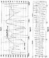
Figure 22 may be examined. As shown inFigure 23 , a 250 MHz clock may be added with output TP_CLK_250 and the a phase shift modulator with output TP_FN1. Due to the Phase Shift Modulator, each data bit isphase shift 0 for half the data period andphase shift 180 for the other half. If the data bit is a 1, it isphase 0 for the first half andphase 180 for the second half. If the data bit is a 0, it isphase 180 for the first half andphase 0 for the second half as shown inFigure 24 . In LTspice (the simulation software used in the example), "^" (shown inFigure 23 is an operand that "Convert(s) the expressions to either side to Boolean, then XORs (exclusive ors) the result. - The modulation of the sideband mitigation technique causes each data bit to cancel itself out on the FFT which results in the 1 GHz lobe being eliminated as seen in
Figure 25 , but the other lobes inFigure 22 are worse than before. Zooming in on 867 MHz inFigure 25 and adding phase givesFigure 26 in which the lobe is centered at 867 MHz, the peak is at -11.7 dB and the phase is -24° (and 1GHz is at -7°.) To mitigate the 867 MHz lobe, we add a 867 MHz, 0.368 V amplitude, 245° phase sine wave, V(TP_FN2) to the signal. The results are TP_FN2 and shown inFigures 27 and 28 . Figure 28 shows residual lobes remain from the first mitigation attempt. To mitigate the 868 MHz lobe, add a 868.6 MHz lobe w/ 0.200 amplitude and 250° phase. These results are shown inFigure 29 . These steps can be repeated for elimination of all the lobes above the -20 dB mask thereby enabling a 125 Mbps data rate to fit within a 250 kHz bandwidth FCC allocation. Using this number inEquation 1, the spectral efficiency of the sideband mitigation system is:
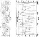
- That is substantially higher the spectral efficiencies of existing technologies. It could be stated that actual spectral efficiency per the standard equation is infinity. The elimination of all the lobes below 1GHz is achieved with the SBM signals shown in Table 1 below and the resultant signal is shown in
Figure 30 and the FFT shown inFigure 31 .TABLE 1 Frequency(MHz) Amplitude(dB) Amplitude(V) Phase(degrees) Phase(radians) 867 -11.7 0.368 244 4.259 868.5 -17.0 0.200 250 4.363 865 -17.5 0.188 162 2.827 883 -10.7 0.413 294.5 5.140 881 -16.6 0.209 22.39 0.391 882 -17.4 0.191 137 2.391 885 -16.22 0.218 22 0.384 - The appropriate characteristics of the neutralizing signal can be determined by a formula in which the data to be transmitted is input into the formula or by a lookup table in which the data to be transmitted is used.
- If information signal in the data wave is phase modulated, phase filtering is useful in the receiver for demodulation Phase modulation is particularly valuable for incoming signals that have noise and interference from nearby data channels. In one example, it is assumed that the incoming signal has the desired data in the signal but the data portion of the signal is obscured by noise and interference in the signal. To perform the phase filtering, an assumption of the value (e.g., a 1 or a 0) of the data is made and a signal equivalent to that assumption is injected into the incoming signal. If the assumption of the data value is correct, constructive interference between the incoming signal and the injected signal will provide constructive interference and verify the assumption. If the assumption of the data value is wrong, destructive interference will show the assumption to be wrong. If the incoming signal and the injected signal are in a resonant (or "tuned") circuit, the difference in the output signal between a correct and incorrect assumption will be quite substantial. This is because the correct assumption on the injected signal and the incoming data portion of the data signal will increase the output signal's amplitude every wave.
- In one embodiment shown in
Figure 32 , the incoming signal may be split 1505 into 2 circuits wherein onecircuit 1501 assumes that the data is a "1" and theother circuit 1502 assumes the data is a "0". Thesignal generators Resistors 1506 are used to add the input signal to the simulated signals. If all four of the resistors shown are the same value, the signals will all be added evenly. If gain is required for specific signals, the resistors of different values can be used. The output from these two circuits may be run through asignal comparison device 1507 and the output of the signal comparison device provides a signal with a strong indication of which assumption ("0" or "1") is the correct assumption. While this output signal will be significantly different than normal wireless signals to be demodulated, it can be analyzed with well known techniques using standard circuitry or digital signal processors (DSP). - It should be noted that while hardware circuits are shown throughout this disclosure to illustrate how specific signals can be generated, these signals and the functions of the hardware can be synthesized through a variety of means which include but are not limited to: digital signal synthesis, waveform generator, arbitrary waveform generator, signal generator, function generator, digital pattern generator, frequency generator, frequency synthesis, direct digital synthesis, etc. For the purpose of this disclosure, all these terms and various hardware solutions are all synonymous and are to be within the scope of this disclosure.
- While the foregoing has been with reference to a particular embodiment of the invention, it will be appreciated by those skilled in the art that changes in this embodiment may be made without departing from the scope of the invention which is defined by the appended claims.


Claims (9)
- A communications apparatus, comprising:a transmitter (401) for transmitting a channel (404) across a transmission line (403), the transmitter (401) further comprises a carrier wave source that provides a carrier wave (501) having a frequency and a circuit that changes a characteristic of the carrier wave (501) wherein the changing of the characteristic of the carrier wave (501) causes a substantial reduction in the average power at the frequency of the carrier wave (501),wherein the circuit that changes a characteristic of the carrier wave (501) further comprises a neutralizing signal generator that injects a neutralizing signal having a characteristic into the transmission line that neutralizes one or more sidebands at one or more sideband frequencies of the carrier wave (501) wherein the neutralizing signal destructively interferes with the one or more sidebands at one or more sideband frequencies.
- The apparatus of claim 1, wherein the characteristic of the carrier wave (501) further comprises a phase of the carrier wave (501) and wherein the circuit that changes a characteristic of the carrier wave (501) further comprises a circuit that shifts the phase of the carrier wave (501) in such a manner that there is a substantial reduction in the average power at the carrier frequency.
- The apparatus of claim 1, wherein the characteristic of the neutralizing signal is determined by a formula in which the data (502) to be transmitted is input into the formula.
- The apparatus of claim 1, wherein the characteristic of the neutralizing signal is determined by a lookup table in which the data (502) to be transmitted is used.
- The apparatus of claim 1, wherein the characteristic of the carrier wave (501) is selected from a group consisting of a phase of the carrier wave, an amplitude of the carrier wave and a frequency of the carrier wave.
- The apparatus of claim 1, wherein the circuit that changes characteristic of the carrier wave (501) further comprises a modulator (503).
- A communications method, comprising:providing a carrier wave (501) having a frequency; andchanging a characteristic of the carrier wave (501) wherein the changing of the characteristic of the carrier wave (501) causes a substantial reduction in the average power at the frequency of the carrier wave (501),wherein changing the characteristic of the carrier wave (501) further comprises injecting a neutralizing signal having a characteristic into the transmission line that neutralizes one or more sidebands at one or more sideband frequencies of the carrier wave (501) wherein the neutralizing signal destructively interferes with the one or more sidebands at one or more sideband frequencies.
- The method of claim 7, wherein changing the characteristic of the carrier wave (501) further comprises shifting the phase of the carrier wave (501) in such a manner that there is a substantial reduction in the average power at the carrier frequency.
- The method of claim 7, wherein the characteristic of the carrier wave (501) is selected from a group consisting of a phase of the carrier wave, an amplitude of the carrier wave and a frequency of the carrier wave.
Applications Claiming Priority (3)
| Application Number | Priority Date | Filing Date | Title |
|---|---|---|---|
| US1504307P | 2007-12-19 | 2007-12-19 | |
| EP08867278.7AEP2235967B1 (en) | 2007-12-19 | 2008-12-19 | Common wave and sideband mitigation communication systems and methods for increasing communication speeds,spectral efficiency and enabling other benefits |
| PCT/US2008/087812WO2009086185A2 (en) | 2007-12-19 | 2008-12-19 | Common wave and sideband mitigation communication systems and methods for increasing communication speeds,spectral efficiency and enabling other benefits |
Related Parent Applications (1)
| Application Number | Title | Priority Date | Filing Date |
|---|---|---|---|
| EP08867278.7ADivisionEP2235967B1 (en) | 2007-12-19 | 2008-12-19 | Common wave and sideband mitigation communication systems and methods for increasing communication speeds,spectral efficiency and enabling other benefits |
Publications (2)
| Publication Number | Publication Date |
|---|---|
| EP3512218A1 EP3512218A1 (en) | 2019-07-17 |
| EP3512218B1true EP3512218B1 (en) | 2021-08-25 |
Family
ID=40825051
Family Applications (2)
| Application Number | Title | Priority Date | Filing Date |
|---|---|---|---|
| EP19154144.0AActiveEP3512218B1 (en) | 2007-12-19 | 2008-12-19 | Common wave and sideband mitigation communication systems and methods for increasing communication speeds,spectral efficiency and enabling other benefits |
| EP08867278.7ANot-in-forceEP2235967B1 (en) | 2007-12-19 | 2008-12-19 | Common wave and sideband mitigation communication systems and methods for increasing communication speeds,spectral efficiency and enabling other benefits |
Family Applications After (1)
| Application Number | Title | Priority Date | Filing Date |
|---|---|---|---|
| EP08867278.7ANot-in-forceEP2235967B1 (en) | 2007-12-19 | 2008-12-19 | Common wave and sideband mitigation communication systems and methods for increasing communication speeds,spectral efficiency and enabling other benefits |
Country Status (7)
| Country | Link |
|---|---|
| US (6) | US8437414B2 (en) |
| EP (2) | EP3512218B1 (en) |
| JP (3) | JP2011508537A (en) |
| KR (1) | KR101525968B1 (en) |
| CN (3) | CN103259751B (en) |
| PH (1) | PH12014502487A1 (en) |
| WO (1) | WO2009086185A2 (en) |
Families Citing this family (7)
| Publication number | Priority date | Publication date | Assignee | Title |
|---|---|---|---|---|
| EP3512218B1 (en) | 2007-12-19 | 2021-08-25 | Falcon Nano, Inc. | Common wave and sideband mitigation communication systems and methods for increasing communication speeds,spectral efficiency and enabling other benefits |
| DK2358423T3 (en)* | 2008-12-15 | 2025-05-12 | Merit Medical Systems Inc | SYSTEM AND METHOD FOR INFLATION SYRINGE DISPLAY AND MODULAR COMPONENT UNIT |
| US8750792B2 (en)* | 2012-07-26 | 2014-06-10 | Remec Broadband Wireless, Llc | Transmitter for point-to-point radio system |
| CN103078679B (en)* | 2013-01-15 | 2017-02-08 | 福建省电力有限公司 | Temporary communication method between transformer substation under construction and built transformer substation or power grid node and microwave relay-optical fiber composite overhead ground wire (OPGW) optical fiber communication link |
| JP7039864B2 (en)* | 2017-05-18 | 2022-03-23 | ソニーグループ株式会社 | Transmitter, receiver, method and recording medium |
| CN111641466B (en)* | 2019-03-01 | 2021-04-20 | 天津工业大学 | Long-distance seawater channel frequency transmission characteristic modeling method based on current field mode |
| CN117043752A (en) | 2021-03-29 | 2023-11-10 | 美光科技公司 | Sideband communication management |
Family Cites Families (57)
| Publication number | Priority date | Publication date | Assignee | Title |
|---|---|---|---|---|
| US3084329A (en)* | 1959-08-06 | 1963-04-02 | Electronic Communications | Noise suppression technique for radio circuits |
| US3701023A (en)* | 1971-06-29 | 1972-10-24 | Ibm | Phase jitter extraction method for data transmission systems |
| US4019140A (en)* | 1975-10-24 | 1977-04-19 | Bell Telephone Laboratories, Incorporated | Methods and apparatus for reducing intelligible crosstalk in single sideband radio systems |
| US4170764A (en)* | 1978-03-06 | 1979-10-09 | Bell Telephone Laboratories, Incorporated | Amplitude and frequency modulation system |
| US4445118A (en)* | 1981-05-22 | 1984-04-24 | The United States Of America As Represented By The Administrator Of The National Aeronautics And Space Administration | Navigation system and method |
| JPH0761146B2 (en)* | 1986-09-19 | 1995-06-28 | 株式会社日立製作所 | Transmission signal reproduction device |
| US5206933A (en)* | 1990-03-15 | 1993-04-27 | International Business Machines Corporation | Data link controller with channels selectively allocatable to hyper channels and hyper channel data funneled through reference logical channels |
| US6693951B1 (en) | 1990-06-25 | 2004-02-17 | Qualcomm Incorporated | System and method for generating signal waveforms in a CDMA cellular telephone system |
| IL100213A (en) | 1990-12-07 | 1995-03-30 | Qualcomm Inc | CDMA microcellular telephone system and distributed antenna system therefor |
| JP3344004B2 (en)* | 1993-06-30 | 2002-11-11 | カシオ計算機株式会社 | Digital modulator |
| JP2872012B2 (en)* | 1993-09-28 | 1999-03-17 | 日本電気株式会社 | Channel selection method and data receiving device |
| JPH07226710A (en)* | 1994-02-16 | 1995-08-22 | Matsushita Electric Ind Co Ltd | CDMA / TDD wireless communication system |
| US5621471A (en)* | 1994-05-03 | 1997-04-15 | Microsoft Corporation | System and method for inserting and recovering an add-on data signal for transmission with a video signal |
| FI97583C (en)* | 1995-02-02 | 1997-01-10 | Nokia Mobile Phones Ltd | Procedure for data communication, transmitters and receivers |
| FI97581C (en)* | 1995-02-10 | 1997-01-10 | Nokia Telecommunications Oy | Receiver and method for generating spreading codes in the receiver |
| US6049535A (en) | 1996-06-27 | 2000-04-11 | Interdigital Technology Corporation | Code division multiple access (CDMA) communication system |
| US6885652B1 (en) | 1995-06-30 | 2005-04-26 | Interdigital Technology Corporation | Code division multiple access (CDMA) communication system |
| US6801516B1 (en) | 1995-06-30 | 2004-10-05 | Interdigital Technology Corporation | Spread-spectrum system for assigning information signals having different data rates |
| JPH09153882A (en)* | 1995-09-25 | 1997-06-10 | Victor Co Of Japan Ltd | Orthogonal frequency division multiple signal transmission system, transmitting device and receiving device |
| US5841396A (en)* | 1996-03-08 | 1998-11-24 | Snaptrack, Inc. | GPS receiver utilizing a communication link |
| JPH10135826A (en) | 1996-09-05 | 1998-05-22 | Sanyo Electric Co Ltd | Pll frequency synthesizer |
| FI972592A7 (en)* | 1997-06-17 | 1998-12-18 | Nokia Corp | Synchronization method |
| JP3667960B2 (en)* | 1997-11-04 | 2005-07-06 | 日本放送協会 | OFDM transmission method, transmitter, and receiver |
| JPH10262028A (en)* | 1998-03-25 | 1998-09-29 | Matsushita Electric Ind Co Ltd | CDMA wireless multiplex transmitting apparatus, CDMA wireless multiplex transmitting apparatus, and CDMA wireless multiplex transmitting method |
| US6535722B1 (en)* | 1998-07-09 | 2003-03-18 | Sarnoff Corporation | Television tuner employing micro-electro-mechanically-switched tuning matrix |
| JP2000201134A (en)* | 1999-01-06 | 2000-07-18 | Ntt Mobil Communication Network Inc | Method for transmitting multi-carrier/ds-cdma and demodulation device |
| US6424074B2 (en)* | 1999-01-14 | 2002-07-23 | The Regents Of The University Of Michigan | Method and apparatus for upconverting and filtering an information signal utilizing a vibrating micromechanical device |
| US6587515B1 (en) | 1999-02-10 | 2003-07-01 | Hamid Jafarkhani | Differential transmitter diversity technique for wireless communications |
| US6658045B1 (en) | 1999-02-22 | 2003-12-02 | Nortel Networks Limited | CDMA communications system adaptive to mobile unit speed |
| JP2000295118A (en)* | 1999-04-01 | 2000-10-20 | Oki Electric Ind Co Ltd | Transmitter |
| JP3715141B2 (en)* | 1999-07-13 | 2005-11-09 | 松下電器産業株式会社 | Communication terminal device |
| US7170954B2 (en) | 1999-07-16 | 2007-01-30 | Lucent Technologies Inc. | Cayley-encodation of unitary matrices for differential communication |
| US6724842B1 (en) | 1999-07-16 | 2004-04-20 | Lucent Technologies Inc. | Method for wireless differential communication using multiple transmitter antennas |
| US6891897B1 (en) | 1999-07-23 | 2005-05-10 | Nortel Networks Limited | Space-time coding and channel estimation scheme, arrangement and method |
| US6975666B2 (en) | 1999-12-23 | 2005-12-13 | Institut National De La Recherche Scientifique | Interference suppression in CDMA systems |
| US6594508B1 (en) | 2000-03-31 | 2003-07-15 | Nokia Corporation | Antenna and cable monitoring for radio base station |
| JP2001298496A (en)* | 2000-04-13 | 2001-10-26 | Oki Electric Ind Co Ltd | Frequency band limiting method |
| US6449302B2 (en)* | 2000-04-19 | 2002-09-10 | Powerwave Technologies, Inc. | System and method for peak power reduction in spread spectrum communications systems |
| US6466168B1 (en) | 2000-08-17 | 2002-10-15 | Mcewen Technologies, Llc | Differential time of flight measurement system |
| JP3947770B2 (en) | 2001-03-12 | 2007-07-25 | 直樹 末広 | CDMA communication system using multiple spreading sequences |
| JP4415518B2 (en)* | 2001-08-15 | 2010-02-17 | 横浜ゴム株式会社 | Transmitter and wireless transmission system |
| US7035284B2 (en)* | 2002-03-14 | 2006-04-25 | Qualcomm Incorporated | Method and apparatus for reducing inter-channel interference in a wireless communication system employing a non-periodic interleaver |
| FR2837647B1 (en)* | 2002-03-25 | 2006-11-24 | Canon Kk | WIRELESS TRANSMITTER WITH REDUCED POWER CONSUMPTION |
| US7050405B2 (en) | 2002-08-23 | 2006-05-23 | Qualcomm Incorporated | Method and system for a data transmission in a communication system |
| US7139274B2 (en) | 2002-08-23 | 2006-11-21 | Qualcomm, Incorporated | Method and system for a data transmission in a communication system |
| US7092717B2 (en) | 2002-12-20 | 2006-08-15 | Qualcomm Incorporated | Method and system for a dynamic adjustment of a data request channel in a communication system |
| CN1732637A (en) | 2002-12-30 | 2006-02-08 | 皇家飞利浦电子股份有限公司 | Apparatus enabled for optimizing spectral efficiency of a wireless link |
| KR100959208B1 (en)* | 2003-03-19 | 2010-05-19 | 엘지전자 주식회사 | How to detect duplicate scheduled recording time |
| US7269205B2 (en)* | 2003-09-26 | 2007-09-11 | Telefonaktiebolaget Lm Ericsson (Publ) | Method and apparatus for signal demodulation |
| US7680201B2 (en)* | 2004-01-26 | 2010-03-16 | Ibiquity Digital Corporation | Forward error correction coding for AM 9kHz and 10kHz in-band on-channel digital audio broadcasting systems |
| JP4546145B2 (en)* | 2004-05-11 | 2010-09-15 | モトローラ・インコーポレイテッド | Multi-carrier transmission system and multi-carrier transmission receiver |
| US7292827B2 (en) | 2004-10-29 | 2007-11-06 | Freescale Semiconductor, Inc. | System and method for providing a single-ended receive portion and a differential transmit portion in a wireless transceiver |
| TWI266489B (en) | 2005-06-07 | 2006-11-11 | Realtek Semiconductor Corp | Apparatus and method for increasing signal estimation accuraccy |
| US20070115160A1 (en) | 2005-11-18 | 2007-05-24 | Bendik Kleveland | Self-referenced differential decoding of analog baseband signals |
| US20070126522A1 (en)* | 2005-12-05 | 2007-06-07 | Skywave Communications, Llc | Control for communication systems transmitting and receiving signals with substantially no sidebands |
| CA2576778C (en)* | 2006-02-07 | 2014-09-02 | Xinping Huang | Self-calibrating multi-port circuit and method |
| EP3512218B1 (en) | 2007-12-19 | 2021-08-25 | Falcon Nano, Inc. | Common wave and sideband mitigation communication systems and methods for increasing communication speeds,spectral efficiency and enabling other benefits |
- 2008
- 2008-12-19EPEP19154144.0Apatent/EP3512218B1/enactiveActive
- 2008-12-19WOPCT/US2008/087812patent/WO2009086185A2/enactiveApplication Filing
- 2008-12-19JPJP2010539903Apatent/JP2011508537A/enactivePending
- 2008-12-19CNCN201310067805.3Apatent/CN103259751B/ennot_activeExpired - Fee Related
- 2008-12-19CNCN2008801271412Apatent/CN101953177A/enactivePending
- 2008-12-19KRKR1020107016052Apatent/KR101525968B1/ennot_activeExpired - Fee Related
- 2008-12-19EPEP08867278.7Apatent/EP2235967B1/ennot_activeNot-in-force
- 2008-12-19CNCN201610084975.6Apatent/CN105610751B/ennot_activeExpired - Fee Related
- 2010
- 2010-07-19USUS12/839,300patent/US8437414B2/ennot_activeExpired - Fee Related
- 2013
- 2013-01-30USUS13/754,849patent/US8861625B2/enactiveActive
- 2013-06-10JPJP2013122277Apatent/JP5740434B2/ennot_activeExpired - Fee Related
- 2014
- 2014-10-08USUS14/510,066patent/US9118525B2/ennot_activeExpired - Fee Related
- 2014-11-07PHPH12014502487Apatent/PH12014502487A1/enunknown
- 2015
- 2015-04-27JPJP2015090716Apatent/JP2015173469A/enactivePending
- 2015-08-24USUS14/834,366patent/US9614696B2/ennot_activeExpired - Fee Related
- 2017
- 2017-03-31USUS15/476,507patent/US10243769B2/ennot_activeExpired - Fee Related
- 2019
- 2019-03-25USUS16/364,076patent/US20190288889A1/ennot_activeAbandoned
Also Published As
| Publication number | Publication date |
|---|---|
| US20190288889A1 (en) | 2019-09-19 |
| PH12014502487B1 (en) | 2015-09-02 |
| CN105610751A (en) | 2016-05-25 |
| CN101953177A (en) | 2011-01-19 |
| KR20100106500A (en) | 2010-10-01 |
| JP5740434B2 (en) | 2015-06-24 |
| WO2009086185A2 (en) | 2009-07-09 |
| US20150365261A1 (en) | 2015-12-17 |
| JP2013225888A (en) | 2013-10-31 |
| JP2011508537A (en) | 2011-03-10 |
| WO2009086185A3 (en) | 2009-12-30 |
| US10243769B2 (en) | 2019-03-26 |
| CN103259751B (en) | 2016-04-20 |
| US20110110456A1 (en) | 2011-05-12 |
| US9118525B2 (en) | 2015-08-25 |
| US20130142281A1 (en) | 2013-06-06 |
| KR101525968B1 (en) | 2015-06-10 |
| US20170207939A1 (en) | 2017-07-20 |
| US8861625B2 (en) | 2014-10-14 |
| EP2235967B1 (en) | 2019-01-30 |
| PH12014502487A1 (en) | 2015-09-02 |
| US8437414B2 (en) | 2013-05-07 |
| CN105610751B (en) | 2019-07-23 |
| EP2235967A4 (en) | 2015-05-20 |
| JP2015173469A (en) | 2015-10-01 |
| EP2235967A2 (en) | 2010-10-06 |
| EP3512218A1 (en) | 2019-07-17 |
| CN103259751A (en) | 2013-08-21 |
| US20150055718A1 (en) | 2015-02-26 |
| US9614696B2 (en) | 2017-04-04 |
Similar Documents
| Publication | Publication Date | Title |
|---|---|---|
| US10243769B2 (en) | Communication apparatus for increasing communication speeds, spectral efficiency and enabling other benefits | |
| US8175134B1 (en) | Radio communications system and method having decreased capability for detection by an adversary | |
| CN109507661B (en) | Radar and communication integrated signal processing method | |
| GB2285371A (en) | DS/SS-CDMA up-link access | |
| JP2004274769A (en) | Method for using modulation scheme for communication, offset chirp modulation transmitter-receiver, method for using offset chirp modulation for communication, and generation system of modulation scheme for communication | |
| CN104483682B (en) | S-band unified TT&C system and its sidetone extraction module and range tone retransmission method | |
| Wang et al. | Sisyphus: Redefining Low Power for LoRa Receiver | |
| US10313166B2 (en) | Backward-compatible signal variations for data augmentation | |
| US6519281B1 (en) | Jitter measurement | |
| US8068573B1 (en) | Phase dithered digital communications system | |
| US8634445B2 (en) | Pulse modulation and demodulation in a multiband UWB communication system | |
| Honek | SDR OFDM frame generation according to IEEE 802.22: OFDMA modulation scheme for sub-GHz band | |
| Honek | SDR OFDM Frame Generation according to IEEE 802.22 | |
| Gil Sorribes | Robust Tracking System in front of Radio-Frequency Interferences. Part 3: Signals, Modulations, and Reliability analysis | |
| Petrović et al. | Bit error probability of PSK systems in the presence of impulse noise | |
| JP2001326580A (en) | Signal detection circuit | |
| JP2007116644A (en) | General-purpose, highly efficient digital ssb radio equipment |
Legal Events
| Date | Code | Title | Description |
|---|---|---|---|
| PUAI | Public reference made under article 153(3) epc to a published international application that has entered the european phase | Free format text:ORIGINAL CODE: 0009012 | |
| STAA | Information on the status of an ep patent application or granted ep patent | Free format text:STATUS: THE APPLICATION HAS BEEN PUBLISHED | |
| AC | Divisional application: reference to earlier application | Ref document number:2235967 Country of ref document:EP Kind code of ref document:P | |
| AK | Designated contracting states | Kind code of ref document:A1 Designated state(s):AT BE BG CH CY CZ DE DK EE ES FI FR GB GR HR HU IE IS IT LI LT LU LV MC MT NL NO PL PT RO SE SI SK TR | |
| STAA | Information on the status of an ep patent application or granted ep patent | Free format text:STATUS: REQUEST FOR EXAMINATION WAS MADE | |
| 17P | Request for examination filed | Effective date:20200117 | |
| RBV | Designated contracting states (corrected) | Designated state(s):AT BE BG CH CY CZ DE DK EE ES FI FR GB GR HR HU IE IS IT LI LT LU LV MC MT NL NO PL PT RO SE SI SK TR | |
| RIC1 | Information provided on ipc code assigned before grant | Ipc:H04L 27/34 20060101ALI20210129BHEP Ipc:H04L 27/18 20060101ALI20210129BHEP Ipc:H04W 4/00 20180101AFI20210129BHEP | |
| GRAP | Despatch of communication of intention to grant a patent | Free format text:ORIGINAL CODE: EPIDOSNIGR1 | |
| STAA | Information on the status of an ep patent application or granted ep patent | Free format text:STATUS: GRANT OF PATENT IS INTENDED | |
| INTG | Intention to grant announced | Effective date:20210312 | |
| GRAS | Grant fee paid | Free format text:ORIGINAL CODE: EPIDOSNIGR3 | |
| GRAA | (expected) grant | Free format text:ORIGINAL CODE: 0009210 | |
| STAA | Information on the status of an ep patent application or granted ep patent | Free format text:STATUS: THE PATENT HAS BEEN GRANTED | |
| AC | Divisional application: reference to earlier application | Ref document number:2235967 Country of ref document:EP Kind code of ref document:P | |
| AK | Designated contracting states | Kind code of ref document:B1 Designated state(s):AT BE BG CH CY CZ DE DK EE ES FI FR GB GR HR HU IE IS IT LI LT LU LV MC MT NL NO PL PT RO SE SI SK TR | |
| REG | Reference to a national code | Ref country code:CH Ref legal event code:EP | |
| REG | Reference to a national code | Ref country code:DE Ref legal event code:R096 Ref document number:602008064192 Country of ref document:DE | |
| REG | Reference to a national code | Ref country code:IE Ref legal event code:FG4D Ref country code:AT Ref legal event code:REF Ref document number:1425071 Country of ref document:AT Kind code of ref document:T Effective date:20210915 | |
| REG | Reference to a national code | Ref country code:LT Ref legal event code:MG9D | |
| REG | Reference to a national code | Ref country code:SE Ref legal event code:TRGR | |
| REG | Reference to a national code | Ref country code:NL Ref legal event code:MP Effective date:20210825 | |
| REG | Reference to a national code | Ref country code:AT Ref legal event code:MK05 Ref document number:1425071 Country of ref document:AT Kind code of ref document:T Effective date:20210825 | |
| PG25 | Lapsed in a contracting state [announced via postgrant information from national office to epo] | Ref country code:FI Free format text:LAPSE BECAUSE OF FAILURE TO SUBMIT A TRANSLATION OF THE DESCRIPTION OR TO PAY THE FEE WITHIN THE PRESCRIBED TIME-LIMIT Effective date:20210825 Ref country code:ES Free format text:LAPSE BECAUSE OF FAILURE TO SUBMIT A TRANSLATION OF THE DESCRIPTION OR TO PAY THE FEE WITHIN THE PRESCRIBED TIME-LIMIT Effective date:20210825 Ref country code:PT Free format text:LAPSE BECAUSE OF FAILURE TO SUBMIT A TRANSLATION OF THE DESCRIPTION OR TO PAY THE FEE WITHIN THE PRESCRIBED TIME-LIMIT Effective date:20211227 Ref country code:NO Free format text:LAPSE BECAUSE OF FAILURE TO SUBMIT A TRANSLATION OF THE DESCRIPTION OR TO PAY THE FEE WITHIN THE PRESCRIBED TIME-LIMIT Effective date:20211125 Ref country code:HR Free format text:LAPSE BECAUSE OF FAILURE TO SUBMIT A TRANSLATION OF THE DESCRIPTION OR TO PAY THE FEE WITHIN THE PRESCRIBED TIME-LIMIT Effective date:20210825 Ref country code:BG Free format text:LAPSE BECAUSE OF FAILURE TO SUBMIT A TRANSLATION OF THE DESCRIPTION OR TO PAY THE FEE WITHIN THE PRESCRIBED TIME-LIMIT Effective date:20211125 Ref country code:AT Free format text:LAPSE BECAUSE OF FAILURE TO SUBMIT A TRANSLATION OF THE DESCRIPTION OR TO PAY THE FEE WITHIN THE PRESCRIBED TIME-LIMIT Effective date:20210825 Ref country code:LT Free format text:LAPSE BECAUSE OF FAILURE TO SUBMIT A TRANSLATION OF THE DESCRIPTION OR TO PAY THE FEE WITHIN THE PRESCRIBED TIME-LIMIT Effective date:20210825 | |
| PGFP | Annual fee paid to national office [announced via postgrant information from national office to epo] | Ref country code:FR Payment date:20211116 Year of fee payment:14 Ref country code:DE Payment date:20211110 Year of fee payment:14 Ref country code:GB Payment date:20211116 Year of fee payment:14 Ref country code:SE Payment date:20211130 Year of fee payment:14 | |
| PG25 | Lapsed in a contracting state [announced via postgrant information from national office to epo] | Ref country code:PL Free format text:LAPSE BECAUSE OF FAILURE TO SUBMIT A TRANSLATION OF THE DESCRIPTION OR TO PAY THE FEE WITHIN THE PRESCRIBED TIME-LIMIT Effective date:20210825 Ref country code:LV Free format text:LAPSE BECAUSE OF FAILURE TO SUBMIT A TRANSLATION OF THE DESCRIPTION OR TO PAY THE FEE WITHIN THE PRESCRIBED TIME-LIMIT Effective date:20210825 Ref country code:GR Free format text:LAPSE BECAUSE OF FAILURE TO SUBMIT A TRANSLATION OF THE DESCRIPTION OR TO PAY THE FEE WITHIN THE PRESCRIBED TIME-LIMIT Effective date:20211126 | |
| PG25 | Lapsed in a contracting state [announced via postgrant information from national office to epo] | Ref country code:NL Free format text:LAPSE BECAUSE OF FAILURE TO SUBMIT A TRANSLATION OF THE DESCRIPTION OR TO PAY THE FEE WITHIN THE PRESCRIBED TIME-LIMIT Effective date:20210825 | |
| PG25 | Lapsed in a contracting state [announced via postgrant information from national office to epo] | Ref country code:DK Free format text:LAPSE BECAUSE OF FAILURE TO SUBMIT A TRANSLATION OF THE DESCRIPTION OR TO PAY THE FEE WITHIN THE PRESCRIBED TIME-LIMIT Effective date:20210825 | |
| REG | Reference to a national code | Ref country code:DE Ref legal event code:R097 Ref document number:602008064192 Country of ref document:DE | |
| PG25 | Lapsed in a contracting state [announced via postgrant information from national office to epo] | Ref country code:SK Free format text:LAPSE BECAUSE OF FAILURE TO SUBMIT A TRANSLATION OF THE DESCRIPTION OR TO PAY THE FEE WITHIN THE PRESCRIBED TIME-LIMIT Effective date:20210825 Ref country code:RO Free format text:LAPSE BECAUSE OF FAILURE TO SUBMIT A TRANSLATION OF THE DESCRIPTION OR TO PAY THE FEE WITHIN THE PRESCRIBED TIME-LIMIT Effective date:20210825 Ref country code:EE Free format text:LAPSE BECAUSE OF FAILURE TO SUBMIT A TRANSLATION OF THE DESCRIPTION OR TO PAY THE FEE WITHIN THE PRESCRIBED TIME-LIMIT Effective date:20210825 Ref country code:CZ Free format text:LAPSE BECAUSE OF FAILURE TO SUBMIT A TRANSLATION OF THE DESCRIPTION OR TO PAY THE FEE WITHIN THE PRESCRIBED TIME-LIMIT Effective date:20210825 | |
| PLBE | No opposition filed within time limit | Free format text:ORIGINAL CODE: 0009261 | |
| STAA | Information on the status of an ep patent application or granted ep patent | Free format text:STATUS: NO OPPOSITION FILED WITHIN TIME LIMIT | |
| PG25 | Lapsed in a contracting state [announced via postgrant information from national office to epo] | Ref country code:MC Free format text:LAPSE BECAUSE OF FAILURE TO SUBMIT A TRANSLATION OF THE DESCRIPTION OR TO PAY THE FEE WITHIN THE PRESCRIBED TIME-LIMIT Effective date:20210825 Ref country code:IT Free format text:LAPSE BECAUSE OF FAILURE TO SUBMIT A TRANSLATION OF THE DESCRIPTION OR TO PAY THE FEE WITHIN THE PRESCRIBED TIME-LIMIT Effective date:20210825 | |
| REG | Reference to a national code | Ref country code:CH Ref legal event code:PL | |
| 26N | No opposition filed | Effective date:20220527 | |
| PG25 | Lapsed in a contracting state [announced via postgrant information from national office to epo] | Ref country code:SI Free format text:LAPSE BECAUSE OF FAILURE TO SUBMIT A TRANSLATION OF THE DESCRIPTION OR TO PAY THE FEE WITHIN THE PRESCRIBED TIME-LIMIT Effective date:20210825 | |
| REG | Reference to a national code | Ref country code:BE Ref legal event code:MM Effective date:20211231 | |
| PG25 | Lapsed in a contracting state [announced via postgrant information from national office to epo] | Ref country code:LU Free format text:LAPSE BECAUSE OF NON-PAYMENT OF DUE FEES Effective date:20211219 Ref country code:IE Free format text:LAPSE BECAUSE OF NON-PAYMENT OF DUE FEES Effective date:20211219 | |
| PG25 | Lapsed in a contracting state [announced via postgrant information from national office to epo] | Ref country code:BE Free format text:LAPSE BECAUSE OF NON-PAYMENT OF DUE FEES Effective date:20211231 | |
| PG25 | Lapsed in a contracting state [announced via postgrant information from national office to epo] | Ref country code:LI Free format text:LAPSE BECAUSE OF NON-PAYMENT OF DUE FEES Effective date:20211231 Ref country code:CH Free format text:LAPSE BECAUSE OF NON-PAYMENT OF DUE FEES Effective date:20211231 | |
| PG25 | Lapsed in a contracting state [announced via postgrant information from national office to epo] | Ref country code:CY Free format text:LAPSE BECAUSE OF FAILURE TO SUBMIT A TRANSLATION OF THE DESCRIPTION OR TO PAY THE FEE WITHIN THE PRESCRIBED TIME-LIMIT Effective date:20210825 | |
| REG | Reference to a national code | Ref country code:DE Ref legal event code:R119 Ref document number:602008064192 Country of ref document:DE | |
| PG25 | Lapsed in a contracting state [announced via postgrant information from national office to epo] | Ref country code:HU Free format text:LAPSE BECAUSE OF FAILURE TO SUBMIT A TRANSLATION OF THE DESCRIPTION OR TO PAY THE FEE WITHIN THE PRESCRIBED TIME-LIMIT; INVALID AB INITIO Effective date:20081219 | |
| REG | Reference to a national code | Ref country code:SE Ref legal event code:EUG | |
| GBPC | Gb: european patent ceased through non-payment of renewal fee | Effective date:20221219 | |
| PG25 | Lapsed in a contracting state [announced via postgrant information from national office to epo] | Ref country code:SE Free format text:LAPSE BECAUSE OF NON-PAYMENT OF DUE FEES Effective date:20221220 Ref country code:GB Free format text:LAPSE BECAUSE OF NON-PAYMENT OF DUE FEES Effective date:20221219 Ref country code:DE Free format text:LAPSE BECAUSE OF NON-PAYMENT OF DUE FEES Effective date:20230701 | |
| PG25 | Lapsed in a contracting state [announced via postgrant information from national office to epo] | Ref country code:FR Free format text:LAPSE BECAUSE OF NON-PAYMENT OF DUE FEES Effective date:20221231 | |
| PG25 | Lapsed in a contracting state [announced via postgrant information from national office to epo] | Ref country code:TR Free format text:LAPSE BECAUSE OF FAILURE TO SUBMIT A TRANSLATION OF THE DESCRIPTION OR TO PAY THE FEE WITHIN THE PRESCRIBED TIME-LIMIT Effective date:20210825 | |
| PG25 | Lapsed in a contracting state [announced via postgrant information from national office to epo] | Ref country code:MT Free format text:LAPSE BECAUSE OF FAILURE TO SUBMIT A TRANSLATION OF THE DESCRIPTION OR TO PAY THE FEE WITHIN THE PRESCRIBED TIME-LIMIT Effective date:20210825 |