EP3498891A1 - Electroplating system and pressure device thereof - Google Patents
Electroplating system and pressure device thereofDownload PDFInfo
- Publication number
- EP3498891A1 EP3498891A1EP18152963.7AEP18152963AEP3498891A1EP 3498891 A1EP3498891 A1EP 3498891A1EP 18152963 AEP18152963 AEP 18152963AEP 3498891 A1EP3498891 A1EP 3498891A1
- Authority
- EP
- European Patent Office
- Prior art keywords
- holes
- conduction
- chamber
- electroplating
- pressure device
- Prior art date
- Legal status (The legal status is an assumption and is not a legal conclusion. Google has not performed a legal analysis and makes no representation as to the accuracy of the status listed.)
- Granted
Links
Images


Classifications
- C—CHEMISTRY; METALLURGY
- C25—ELECTROLYTIC OR ELECTROPHORETIC PROCESSES; APPARATUS THEREFOR
- C25D—PROCESSES FOR THE ELECTROLYTIC OR ELECTROPHORETIC PRODUCTION OF COATINGS; ELECTROFORMING; APPARATUS THEREFOR
- C25D5/00—Electroplating characterised by the process; Pretreatment or after-treatment of workpieces
- C25D5/08—Electroplating with moving electrolyte e.g. jet electroplating
- C—CHEMISTRY; METALLURGY
- C25—ELECTROLYTIC OR ELECTROPHORETIC PROCESSES; APPARATUS THEREFOR
- C25D—PROCESSES FOR THE ELECTROLYTIC OR ELECTROPHORETIC PRODUCTION OF COATINGS; ELECTROFORMING; APPARATUS THEREFOR
- C25D17/00—Constructional parts, or assemblies thereof, of cells for electrolytic coating
- C25D17/001—Apparatus specially adapted for electrolytic coating of wafers, e.g. semiconductors or solar cells
- C—CHEMISTRY; METALLURGY
- C25—ELECTROLYTIC OR ELECTROPHORETIC PROCESSES; APPARATUS THEREFOR
- C25D—PROCESSES FOR THE ELECTROLYTIC OR ELECTROPHORETIC PRODUCTION OF COATINGS; ELECTROFORMING; APPARATUS THEREFOR
- C25D17/00—Constructional parts, or assemblies thereof, of cells for electrolytic coating
- C25D17/008—Current shielding devices
- C—CHEMISTRY; METALLURGY
- C25—ELECTROLYTIC OR ELECTROPHORETIC PROCESSES; APPARATUS THEREFOR
- C25D—PROCESSES FOR THE ELECTROLYTIC OR ELECTROPHORETIC PRODUCTION OF COATINGS; ELECTROFORMING; APPARATUS THEREFOR
- C25D17/00—Constructional parts, or assemblies thereof, of cells for electrolytic coating
- C25D17/06—Suspending or supporting devices for articles to be coated
- C—CHEMISTRY; METALLURGY
- C25—ELECTROLYTIC OR ELECTROPHORETIC PROCESSES; APPARATUS THEREFOR
- C25D—PROCESSES FOR THE ELECTROLYTIC OR ELECTROPHORETIC PRODUCTION OF COATINGS; ELECTROFORMING; APPARATUS THEREFOR
- C25D21/00—Processes for servicing or operating cells for electrolytic coating
- C25D21/04—Removal of gases or vapours ; Gas or pressure control
- C—CHEMISTRY; METALLURGY
- C25—ELECTROLYTIC OR ELECTROPHORETIC PROCESSES; APPARATUS THEREFOR
- C25D—PROCESSES FOR THE ELECTROLYTIC OR ELECTROPHORETIC PRODUCTION OF COATINGS; ELECTROFORMING; APPARATUS THEREFOR
- C25D21/00—Processes for servicing or operating cells for electrolytic coating
- C25D21/10—Agitating of electrolytes; Moving of racks
Definitions
- This inventionrelates to an electroplating system and its pressure device.
- the electroplating system placed in an electroplating tank filling with plating solutionis adapted to deposit a plating material on an object.
- a plating object and a metal anode elementare placed in an electroplating tank and electrically connected to a cathode and an anode of a power supply, respectively.
- An electroplating solution filling in the electroplating tankis provided to deposit a plating material onto the plating object.
- the plating objectis a wafer or a circuit board
- the metal anode elementis a copper sheet
- the electroplating solutionis CuSO 4 .
- a copper layer or a copper wirewill be formed on the surface of the plating object when powered on.
- the plating rate of the conventional electroplating processis slower, and bubbles and/or impurities may remain in fine-pitch wires or blind holes of the wafer and circuit board during the conventional electroplating process, so plating defect may occur in the fine-pitch wires or blind holes.
- the object of the present inventionis to prevent plating defect and enhance plating efficiency.
- the electroplating system of the present inventionis adapted to deposit a plating material on an object when placed in an electroplating tank with an electroplating solution.
- the electroplating systemincludes a pressure device and an anode element.
- the pressure deviceincludes a lid and a base.
- the lidhas a first surface, a second surface, first through holes and second through holes. The first surface faces toward the object and the first and second surfaces are communicated with each other through the first and second through holes.
- the basehas a third surface, a chamber recessed on the third surface, conduction tubes and third through holes.
- the third through holesare formed in the chamber and penetrate through the base.
- the conduction tubesare positioned in the chamber and each includes a conduction hole, and each of the conduction holes connects to one of the third through holes.
- the lidcovers an opening of the chamber, the first through holes communicate with the chamber and each of the second through holes reveals one of the conduction holes.
- the electroplating solution in the chamberis able to be sprayed toward the object through the first through holes.
- the conduction holes and the third through hole connected with each otherbecome a passage of electric force line.
- the anode elementis disposed outside the pressure device. The object is located outside a first end of the passage of electric force line and the anode element is located outside a second end of the passage of electric force line.
- the electroplating solutionfilled and pressed in the chamber, can spray toward the object through the first through holes and wash the bubbles and/or impurities remained on the object to prevent plating defect and enhance plating efficiency. Furthermore, the passage of electric force line formed in the conduction holes and the third through holes provides a benefit for the deposition of the plating material on the object.
- an electroplating system 10 of the present inventioncan be placed in an electroplating tank 20 with an electroplating solution 30 to deposit a plating material on an object 40.
- the object 40is, but not limited to, a wafer or a circuit board.
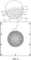
- the electroplating system 10includes a pressure device 100 and an anode element 200 positioned outside the pressure device 100.
- the anode element 200is a titanium basket which can accommodate a metal piece.
- the electroplating system 10further includes a carrier 300 and the pressure device 100 is connected to the carrier 300 in this embodiment.
- the carrier 300has an accommodation space 310 where the anode element 200 is placed.
- the electroplating system 10further includes a frame 400 which is positioned in the accommodation space 310.
- the anode element 200is placed in the frame 400, and furthermore, the anode element 200 (e.g. titanium basket) and/or the frame 400 are replaceable.
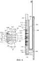
- the pressure device 100includes a lid 110 and a base 120.
- the lid 110has a first surface 111, a second surface 112, first through holes 113 and second through holes 114.
- the first surface 111faces toward the object 40 when the electroplating system 10 is placed in the electroplating tank 20 filling with the electroplating solution 30.
- the first and second surfaces 111 and 112are communicated with each other via the first and second through holes 113, 114, in other words, the first and second through holes 113, 114 penetrate through the lid 110.
- the first and second through holes 113, 114are aligned radially on the lid 110, and the first through holes 113 have a diameter equal to or smaller than that of the second through holes 114.
- the base 120has a third surface 121, a fourth surface 122, a chamber 123 recessed on the third surface 121, conduction tubes 124 and third through holes 125.
- the third through holes 125are formed in the chamber 123 and penetrate through the base 120.
- the third through holes 125are formed on the bottom 123b and penetrate through the fourth surface 122.
- the conduction tubes 124are positioned in the chamber 123 and each includes a conduction hole 124a.
- the diameter of the first through holes 113is equal to or smaller than that of the conduction holes 124a, and each of the conduction holes 124a is connected with one of the third through holes 125.
- each of the conduction tubes 124 in this embodimentincludes a basal portion 124b and a connecting portion 124c, and each of the conduction holes 124a is formed in the basal portion 124b and the connecting portion 124c.
- the basal portion 124bis connected to the bottom 123b of the chamber 123 and the connecting portion 124c is protruded from the third surface 121.
- each of the conduction tubes 124in this embodiment further includes a supporting portion 124d located between the basal portion 124b and the connecting portion 124c. The supporting portion 124d is adapted to support the lid 110 covering the opening 123a in order to prevent the lid 110 from distorting.
- the pressure device 100 in this embodimentfurther includes at least one feeding pipe 130 which is designed to communicate with the chamber 123.
- the feeding pipe 130is provided to supply the electroplating solution 30 to the chamber 123.
- a motoris utilized to deliver the electroplating solution 30 in the electroplating tank 20 to the chamber 123 through the feeding pipe 130.
- the electroplating solution 30 delivered to the chamber 123 by the feeding pipe 130canbe sprayed through the first through holes 113.
- the smaller the diameter of the first through holes 113the higher impact the electroplating solution 30 sprayed from the first through holes 113.
- the object 40 and the anode element 200can be electrically connected to a cathode and a anode of a DC power supply respectively, allow the conduction holes 124a and the third through holes 125 connected with each other to become a passage of electric force line P.
- the object 40is located outside a first end P1 of the passage of electric force line P and the anode element 200 is located outside a second end P2 of the passage of electric force line P for the deposition of the plating material on the object 40.
- the electroplating solution 30 filling in the chamber 123can be sprayed toward the object 40 through the first through holes 113 to enhance the electroplating efficiency. And the electroplating solution 30 sprayed from the first through holes 113 also can wash the bubbles and/or impurities remained on the object 40 so as to prevent defective plating.
Landscapes
- Chemical & Material Sciences (AREA)
- Engineering & Computer Science (AREA)
- Chemical Kinetics & Catalysis (AREA)
- Electrochemistry (AREA)
- Materials Engineering (AREA)
- Metallurgy (AREA)
- Organic Chemistry (AREA)
- Life Sciences & Earth Sciences (AREA)
- Sustainable Development (AREA)
- Electroplating Methods And Accessories (AREA)
- Electrodes Of Semiconductors (AREA)
Abstract
Description
- This invention relates to an electroplating system and its pressure device. The electroplating system placed in an electroplating tank filling with plating solution is adapted to deposit a plating material on an object.
- In conventional electroplating process, a plating object and a metal anode element are placed in an electroplating tank and electrically connected to a cathode and an anode of a power supply, respectively. An electroplating solution filling in the electroplating tank is provided to deposit a plating material onto the plating object. For instance, the plating object is a wafer or a circuit board, the metal anode element is a copper sheet and the electroplating solution is CuSO4. A copper layer or a copper wire will be formed on the surface of the plating object when powered on.
- However, the plating rate of the conventional electroplating process is slower, and bubbles and/or impurities may remain in fine-pitch wires or blind holes of the wafer and circuit board during the conventional electroplating process, so plating defect may occur in the fine-pitch wires or blind holes.
- The object of the present invention is to prevent plating defect and enhance plating efficiency.
- The electroplating system of the present invention is adapted to deposit a plating material on an object when placed in an electroplating tank with an electroplating solution. The electroplating system includes a pressure device and an anode element. The pressure device includes a lid and a base. The lid has a first surface, a second surface, first through holes and second through holes. The first surface faces toward the object and the first and second surfaces are communicated with each other through the first and second through holes. The base has a third surface, a chamber recessed on the third surface, conduction tubes and third through holes. The third through holes are formed in the chamber and penetrate through the base. The conduction tubes are positioned in the chamber and each includes a conduction hole, and each of the conduction holes connects to one of the third through holes. The lid covers an opening of the chamber, the first through holes communicate with the chamber and each of the second through holes reveals one of the conduction holes. When the electroplating solution is filled in the chamber, the electroplating solution in the chamber is able to be sprayed toward the object through the first through holes. When the electroplating solution is filled in the conduction holes and the third through holes, the conduction holes and the third through hole connected with each other become a passage of electric force line. The anode element is disposed outside the pressure device. The object is located outside a first end of the passage of electric force line and the anode element is located outside a second end of the passage of electric force line.
- The electroplating solution, filled and pressed in the chamber, can spray toward the object through the first through holes and wash the bubbles and/or impurities remained on the object to prevent plating defect and enhance plating efficiency. Furthermore, the passage of electric force line formed in the conduction holes and the third through holes provides a benefit for the deposition of the plating material on the object.
- In the drawings:
Fig. 1 is a perspective assembly diagram illustrating an electroplating system of the present invention.Fig. 2 is a schematic diagram illustrating the electroplating system of the present invention and an object which are placed in an electroplating tank.Fig. 3 is a perspective exploded diagram illustrating the electroplating system of the present invention.Fig. 4 is a front-side view diagram illustrating a lid of a pressure device of the present invention.Fig. 5 is a cross-section view diagram illustrating the pressure device of the present invention.Fig. 6 is a cross-section view diagram illustrating the electroplating system of the present invention.- With reference to
Figs. 1 and2 , anelectroplating system 10 of the present invention can be placed in anelectroplating tank 20 with anelectroplating solution 30 to deposit a plating material on anobject 40. Theobject 40 is, but not limited to, a wafer or a circuit board. - With reference to
Figs. 1 to 3 , theelectroplating system 10 includes apressure device 100 and ananode element 200 positioned outside thepressure device 100. Preferably, theanode element 200 is a titanium basket which can accommodate a metal piece. - With reference to
Figs. 1 to 4 , theelectroplating system 10 further includes acarrier 300 and thepressure device 100 is connected to thecarrier 300 in this embodiment. Thecarrier 300 has anaccommodation space 310 where theanode element 200 is placed. Preferably, theelectroplating system 10 further includes aframe 400 which is positioned in theaccommodation space 310. Theanode element 200 is placed in theframe 400, and furthermore, the anode element 200 (e.g. titanium basket) and/or theframe 400 are replaceable. - With reference to
Figs. 2 to 6 , thepressure device 100 includes alid 110 and abase 120. Thelid 110 has afirst surface 111, asecond surface 112, first throughholes 113 and second throughholes 114. Thefirst surface 111 faces toward theobject 40 when theelectroplating system 10 is placed in theelectroplating tank 20 filling with theelectroplating solution 30. With reference toFigs. 3 to 5 , the first andsecond surfaces holes holes lid 110. Preferably, the first and second throughholes lid 110, and the first throughholes 113 have a diameter equal to or smaller than that of the second throughholes 114. - With reference to
Figs. 3 and5 , thebase 120 has athird surface 121, afourth surface 122, achamber 123 recessed on thethird surface 121,conduction tubes 124 and third throughholes 125. The third throughholes 125 are formed in thechamber 123 and penetrate through thebase 120. There are an opening 123a and abottom 123b in thechamber 123, and the opening 123a reveals thebottom 123b. In this embodiment, the third throughholes 125 are formed on thebottom 123b and penetrate through thefourth surface 122. Theconduction tubes 124 are positioned in thechamber 123 and each includes aconduction hole 124a. Preferably, the diameter of the first throughholes 113 is equal to or smaller than that of theconduction holes 124a, and each of theconduction holes 124a is connected with one of the third throughholes 125. - With reference to
Figs. 3 and5 , each of theconduction tubes 124 in this embodiment includes abasal portion 124b and a connectingportion 124c, and each of theconduction holes 124a is formed in thebasal portion 124b and the connectingportion 124c. Thebasal portion 124b is connected to thebottom 123b of thechamber 123 and the connectingportion 124c is protruded from thethird surface 121. - With reference to
Figs. 3 ,5 and6 , when thelid 110 covers the opening 123a, the first throughholes 113 communicate with thechamber 123 and each of the second throughholes 114 reveals one of theconduction holes 124a. In this embodiment, the connectingportion 124c of each of theconduction tubes 124 is inserted into one of the second throughholes 114, and thefirst surface 111 of thelid 110 and thefourth surface 122 of thebase 120 are communicated with each other through theconduction holes 124a and the third throughholes 125 connected with each other. Moreover, each of theconduction tubes 124 in this embodiment further includes a supportingportion 124d located between thebasal portion 124b and the connectingportion 124c. The supportingportion 124d is adapted to support thelid 110 covering the opening 123a in order to prevent thelid 110 from distorting. - With reference to
Figs. 3 and6 , thepressure device 100 in this embodiment further includes at least onefeeding pipe 130 which is designed to communicate with thechamber 123. When thelid 110 covers the opening 123a of thechamber 123, thefeeding pipe 130 is provided to supply theelectroplating solution 30 to thechamber 123. Preferably, a motor is utilized to deliver theelectroplating solution 30 in theelectroplating tank 20 to thechamber 123 through thefeeding pipe 130. - With reference to
Figs. 4 to 6 , owing to thelid 110 covers the opening 123a of thechamber 123 and the connectingportions 124c of theconduction tubes 124 are inserted into the second throughholes 114, theelectroplating solution 30 delivered to thechamber 123 by thefeeding pipe 130 canbe sprayed through the first throughholes 113. The higher the flow quantity or flow rate of theelectroplating solution 30 delivered to thechamber 123 through thefeeding pipe 130, the higher impact theelectroplating solution 30 sprayed from the first throughholes 113. Besides, the smaller the diameter of the first throughholes 113, the higher impact theelectroplating solution 30 sprayed from the first throughholes 113. - With reference to
Figs. 2 and6 , when theelectroplating system 10 and theobject 40 are placed in theelectroplating tank 20 with theelectroplating solution 30 and theconduction holes 124a and the third throughholes 125 are filled with theelectroplating solution 30, theobject 40 and theanode element 200 can be electrically connected to a cathode and a anode of a DC power supply respectively, allow theconduction holes 124a and the third throughholes 125 connected with each other to become a passage of electric force line P. Theobject 40 is located outside a first end P1 of the passage of electric force line P and theanode element 200 is located outside a second end P2 of the passage of electric force line P for the deposition of the plating material on theobject 40. Otherwise, when theelectroplating solution 30 is delivered to thechamber 123 via thefeeding pipe 130, theelectroplating solution 30 filling in thechamber 123 can be sprayed toward theobject 40 through the first throughholes 113 to enhance the electroplating efficiency. And theelectroplating solution 30 sprayed from the first throughholes 113 also can wash the bubbles and/or impurities remained on theobject 40 so as to prevent defective plating. - While this invention has been particularly illustrated and described in detail with respect to the preferred embodiments thereof, it will be clearly understood by those skilled in the art that is not limited to the specific features shown and described and various modified and changed in form and details may be made without departing from the scope of the claims.
Claims (15)
- A pressure device (100) of an electroplating system (10), the electroplating system (10) is adapted to deposit a plating material on an object (40) when placed in an electroplating tank (20) with an electroplating solution (30), the pressure device (100) comprising:a lid (110) having a first surface (111), a second surface (112), a plurality of first through holes (113) and a plurality of second through holes (114), the first surface (111) faces toward the object (40), the first and second surfaces (111, 112) are communicated with each other through the first and second through holes (113, 114); anda base (120) having a third surface (121), a chamber (123) recessed on the third surface (121), a plurality of conduction tubes (124) and a plurality of third through holes (125), the third through holes (125) are formed in the chamber (123) and penetrate through the base (120), the conduction tubes (124) are positioned in the chamber (123) and each includes a conduction hole (124a), each of the conduction holes (124a) connects to one of the third through holes (125), wherein the lid (110) covers an opening (123a) of the chamber (123), the first through holes (113) communicate with the chamber (123), each of the second through holes (114) reveals one of the conduction holes (124a), and the electroplating solution (30) filled in the chamber (123) is able to be sprayed toward the object (40) through the first through holes (113), and wherein the conduction holes (124a) and the third through holes (125) connected with each other become a passage of electric force line (P) when the electroplating solution (30) is filled in the conduction holes (124a) and the third through holes (125).
- The pressure device (100) in accordance with claim 1, wherein each of the conduction tubes (124) includes a basal portion (124b) and a connecting portion (124c), each of the conduction holes (124a) is formed in the basal portion (124b) and the connecting portion (124c), the basal portion (124b) is connected to a bottom (123b) of the chamber (123) and the third through holes (125) are formed on the bottom (123b), each of the connecting portions (124c) is protruded from the third surface (121) and is inserted into one of the second through holes (114) when the lid (110) covers the opening (123a).
- The pressure device (100) in accordance with claim 2, wherein each of the conduction tubes (124) further includes a supporting portion (124d) located between the basal portion (124b) and the connecting portion (124c) for supporting the lid (110).
- The pressure device (100) in accordance with one of claims 1 to 3, wherein the first through holes (113) have a diameter which is equal to or smaller than that of the second through holes (114).
- The pressure device (100) in accordance with one of claims 1 to 4, wherein the first through holes (113) have a diameter which is equal to or smaller than that of the conduction holes (124a).
- The pressure device (100) in accordance with one of claims 1 to 5, wherein the second through holes (114) are aligned radially on the lid (110).
- An electroplating system (10) adapted to deposit a plating material on an object (40) when placed in an electroplating tank (20) with an electroplating solution (30), comprising:a pressure device (100) including a lid (110) and a base (120), the lid (110) has a first surface (111), a second surface (112), a plurality of first through holes (113) and a plurality of second through holes (114), the first surface (111) faces toward the object (40), the first and second surfaces (111, 112) are communicated with each other through the first and second through holes (113, 114), the base (120) has a third surface (121), a chamber (123) recessed on the third surface (121), a plurality of conduction tubes (124) and a plurality of third through holes (125), the third through holes (125) are formed in the chamber (123) and penetrate through the base (120), the conduction tubes (124) are positioned in the chamber (123) and each includes a conduction hole (124a), each of the conduction holes (124a) connects to one of the third through holes (125), wherein the lid (110) covers an opening (123a) of the chamber (123), the first through holes (113) communicate with the chamber (123), each of the second through holes (114) reveals one of the conduction holes (124a), and the electroplating solution (40) filled in the chamber (123) is able to be sprayed toward the object (40) through the first through holes (113), and wherein the conduction holes (124a) and the third through holes (125) connected with each other become a passage of electric force line (P) when the electroplating solution (30) is filled in the conduction holes (124a) and the third through holes (125); and an anode element (200) disposed outside the pressure device (100), the object (40) is located outside a first end (P1) of the passage of electric force line (P) and the anode element (200) is located outside a second end (P2) of the passage of electric force line (P).
- The electroplating system (10) in accordance with claim 7, wherein the anode element (200) is a titanium basket.
- The electroplating system (10) in accordance with claim 7 or 8 further comprising a carrier (300) having an accommodation space (310), wherein the pressure device (100) is connected to the carrier (300) and the anode element (200) is placed in the accommodation space (310).
- The electroplating system (10) in accordance with claim 7 or 8 further comprising a carrier (300) and a frame (400), wherein the pressure device (100) is connected to the carrier (300) having an accommodation space (310), the anode element (200) is placed in the frame (400), and the frame (400) is placed in the accommodation space (310).
- The electroplating system (10) in accordance with one of claims 7 to 10, wherein each of the conduction tubes (124) includes a basal portion (124b) and a connecting portion (124c), each of the conduction holes (124a) is formed in the basal portion (124b) and the connecting portion (124c), the basal portion (124b) is connected to a bottom (123a) of the chamber (123) and the third through holes (125) are formed on the bottom (123a), each of the connecting portions (124c) is protruded from the third surface (121) and is inserted into one of the second through holes (114) when the lid (110) covers the opening (123a).
- The electroplating system (10) in accordance with claim 11, wherein each of the conduction tubes (124) further includes a supporting portion (124d) located between the basal portion (124b) and the connecting portion (124c) for supporting the lid (110).
- The electroplating system (10) in accordance with one of claims 7 to 12, wherein the first through holes (113) have a diameter which is equal to or smaller than that of the second through holes (114).
- The electroplating system (10) in accordance with one of claims 7 to 13, wherein the first through holes (113) have a diameter which is equal to or smaller than that of the conduction holes (124a).
- The electroplating system (10) in accordance with one of claims 7 to 14, wherein the second through holes (114) are aligned radially on the lid (110).
Applications Claiming Priority (1)
| Application Number | Priority Date | Filing Date | Title |
|---|---|---|---|
| TW106144223ATWI663294B (en) | 2017-12-15 | 2017-12-15 | Electroplating device and pressure chamber thereof |
Publications (2)
| Publication Number | Publication Date |
|---|---|
| EP3498891A1true EP3498891A1 (en) | 2019-06-19 |
| EP3498891B1 EP3498891B1 (en) | 2022-12-14 |
Family
ID=61022223
Family Applications (1)
| Application Number | Title | Priority Date | Filing Date |
|---|---|---|---|
| EP18152963.7AActiveEP3498891B1 (en) | 2017-12-15 | 2018-01-23 | Electroplating system with pressure device |
Country Status (6)
| Country | Link |
|---|---|
| US (1) | US10808331B2 (en) |
| EP (1) | EP3498891B1 (en) |
| JP (1) | JP6568607B2 (en) |
| KR (1) | KR101999558B1 (en) |
| CN (1) | CN109930185B (en) |
| TW (1) | TWI663294B (en) |
Cited By (1)
| Publication number | Priority date | Publication date | Assignee | Title |
|---|---|---|---|---|
| US12351921B2 (en) | 2019-11-22 | 2025-07-08 | Semsysco Gmbh | Distribution body for a process fluid for chemical and/or electrolytic surface treatment of a substrate |
Families Citing this family (2)
| Publication number | Priority date | Publication date | Assignee | Title |
|---|---|---|---|---|
| JP7316908B2 (en)* | 2019-10-30 | 2023-07-28 | 株式会社荏原製作所 | anode assembly |
| JP7356401B2 (en)* | 2020-05-12 | 2023-10-04 | 株式会社荏原製作所 | Plate, plating equipment, and plate manufacturing method |
Citations (4)
| Publication number | Priority date | Publication date | Assignee | Title |
|---|---|---|---|---|
| US20040084318A1 (en)* | 2002-11-05 | 2004-05-06 | Uri Cohen | Methods and apparatus for activating openings and for jets plating |
| US20040094427A1 (en)* | 2002-11-14 | 2004-05-20 | International Business Machines Corporation | Integrated plating and planarization process and apparatus therefor |
| US20050051437A1 (en)* | 2003-09-04 | 2005-03-10 | Keiichi Kurashina | Plating apparatus and plating method |
| EP2598676B1 (en) | 2010-07-29 | 2016-03-30 | Fraunhofer-Gesellschaft zur Förderung der angewandten Forschung e.V. | Device and method for producing targeted flow and current density patterns in a chemical and/or electrolytic surface treatment |
Family Cites Families (12)
| Publication number | Priority date | Publication date | Assignee | Title |
|---|---|---|---|---|
| JP4312465B2 (en)* | 2003-01-23 | 2009-08-12 | 株式会社荏原製作所 | Plating method and plating apparatus |
| JP2004311919A (en) | 2003-02-21 | 2004-11-04 | Shinko Electric Ind Co Ltd | Through-hole filling method |
| JP2004359994A (en) | 2003-06-03 | 2004-12-24 | Sumitomo Bakelite Co Ltd | Electroplating equipment and method |
| JP5650899B2 (en)* | 2009-09-08 | 2015-01-07 | 上村工業株式会社 | Electroplating equipment |
| JP2011241417A (en) | 2010-05-17 | 2011-12-01 | Panasonic Corp | Apparatus and method for manufacturing semiconductor device |
| KR101693217B1 (en)* | 2010-07-20 | 2017-01-05 | 주식회사 케이엠더블유 | Electroplating apparatus |
| CN102191521B (en)* | 2011-05-24 | 2013-01-09 | 厦门永红科技有限公司 | Electroplating device for lead wire framework |
| KR101226663B1 (en) | 2012-08-09 | 2013-01-25 | (주) 탑스 | Anode module and electroplating apparatus having it |
| EP2746432A1 (en) | 2012-12-20 | 2014-06-25 | Atotech Deutschland GmbH | Device for vertical galvanic metal deposition on a substrate |
| KR200480245Y1 (en) | 2013-02-20 | 2016-04-28 | 프로세스 어드밴스 테크놀러지 리미티드 | Plating of injection epuipment box |
| KR101593887B1 (en)* | 2015-10-23 | 2016-02-12 | 선호경 | Spraying apparatus for plating solution on printed circuit board |
| CN206266725U (en)* | 2016-10-18 | 2017-06-20 | 东莞宇宙电路板设备有限公司 | An electroplating device |
- 2017
- 2017-12-15TWTW106144223Apatent/TWI663294B/enactive
- 2017-12-26CNCN201711436261.8Apatent/CN109930185B/enactiveActive
- 2018
- 2018-01-11USUS15/867,878patent/US10808331B2/enactiveActive
- 2018-01-15KRKR1020180004961Apatent/KR101999558B1/enactiveActive
- 2018-01-23EPEP18152963.7Apatent/EP3498891B1/enactiveActive
- 2018-02-02JPJP2018017037Apatent/JP6568607B2/enactiveActive
Patent Citations (4)
| Publication number | Priority date | Publication date | Assignee | Title |
|---|---|---|---|---|
| US20040084318A1 (en)* | 2002-11-05 | 2004-05-06 | Uri Cohen | Methods and apparatus for activating openings and for jets plating |
| US20040094427A1 (en)* | 2002-11-14 | 2004-05-20 | International Business Machines Corporation | Integrated plating and planarization process and apparatus therefor |
| US20050051437A1 (en)* | 2003-09-04 | 2005-03-10 | Keiichi Kurashina | Plating apparatus and plating method |
| EP2598676B1 (en) | 2010-07-29 | 2016-03-30 | Fraunhofer-Gesellschaft zur Förderung der angewandten Forschung e.V. | Device and method for producing targeted flow and current density patterns in a chemical and/or electrolytic surface treatment |
Cited By (2)
| Publication number | Priority date | Publication date | Assignee | Title |
|---|---|---|---|---|
| US12351921B2 (en) | 2019-11-22 | 2025-07-08 | Semsysco Gmbh | Distribution body for a process fluid for chemical and/or electrolytic surface treatment of a substrate |
| EP3825445B1 (en)* | 2019-11-22 | 2025-08-20 | Semsysco GmbH | Distribution body for a process fluid for chemical and/or electrolytic surface treatment of a substrate |
Also Published As
| Publication number | Publication date |
|---|---|
| JP2019108605A (en) | 2019-07-04 |
| US20190186037A1 (en) | 2019-06-20 |
| KR101999558B1 (en) | 2019-07-12 |
| CN109930185A (en) | 2019-06-25 |
| US10808331B2 (en) | 2020-10-20 |
| EP3498891B1 (en) | 2022-12-14 |
| CN109930185B (en) | 2020-08-11 |
| TWI663294B (en) | 2019-06-21 |
| JP6568607B2 (en) | 2019-08-28 |
| TW201928121A (en) | 2019-07-16 |
Similar Documents
| Publication | Publication Date | Title |
|---|---|---|
| EP3498891A1 (en) | Electroplating system and pressure device thereof | |
| JP6222145B2 (en) | Metal film forming apparatus and film forming method | |
| JP5763151B2 (en) | Electrolytic plating shielding plate and electrolytic plating apparatus having the same | |
| US9708724B2 (en) | Anode unit and plating apparatus having such anode unit | |
| WO2010062822A3 (en) | Electrodeposition of copper in microelectronics with dipyridyl-based levelers | |
| JP6517574B2 (en) | Electrolytic plating system | |
| US9714474B2 (en) | Seed layer deposition in microscale features | |
| JP2015221932A (en) | Cathode jig for electroplating and rack for electroplating using the same | |
| CN109477236B (en) | Apparatus for vertical current metal deposition on a substrate | |
| JP6746185B2 (en) | Jig for semiconductor wafer plating | |
| EP4101949B1 (en) | System for a chemical and/or electrolytic surface treatment of a substrate | |
| US5198089A (en) | Plating tank | |
| CN114351226A (en) | Electroplating hanger and electroplating device | |
| KR101153275B1 (en) | Plating jig for electronic parts and electrolysis plating apparatus | |
| CN210657187U (en) | A circuit board vertical continuous electroplating equipment | |
| JP2006016651A (en) | Holder for plating wafer | |
| CN105862114A (en) | A jig for electroplating and a method of manufacturing an electroplated article | |
| US6649034B1 (en) | Electro-chemical metal alloying for semiconductor manufacturing | |
| JP2000273698A (en) | Cathode electrode for wafer plating | |
| CN114351202A (en) | Wafer electroplating method and wafer | |
| KR100748790B1 (en) | Plating apparatus and method | |
| KR20230110781A (en) | Plating device and plating method | |
| CN114351227A (en) | Electroplating hanger and electroplating device | |
| JP2008024986A (en) | Plating method and apparatus | |
| JPH05163599A (en) | Jig for electroplating |
Legal Events
| Date | Code | Title | Description |
|---|---|---|---|
| PUAI | Public reference made under article 153(3) epc to a published international application that has entered the european phase | Free format text:ORIGINAL CODE: 0009012 | |
| STAA | Information on the status of an ep patent application or granted ep patent | Free format text:STATUS: THE APPLICATION HAS BEEN PUBLISHED | |
| AK | Designated contracting states | Kind code of ref document:A1 Designated state(s):AL AT BE BG CH CY CZ DE DK EE ES FI FR GB GR HR HU IE IS IT LI LT LU LV MC MK MT NL NO PL PT RO RS SE SI SK SM TR | |
| AX | Request for extension of the european patent | Extension state:BA ME | |
| STAA | Information on the status of an ep patent application or granted ep patent | Free format text:STATUS: REQUEST FOR EXAMINATION WAS MADE | |
| 17P | Request for examination filed | Effective date:20191129 | |
| RBV | Designated contracting states (corrected) | Designated state(s):AL AT BE BG CH CY CZ DE DK EE ES FI FR GB GR HR HU IE IS IT LI LT LU LV MC MK MT NL NO PL PT RO RS SE SI SK SM TR | |
| STAA | Information on the status of an ep patent application or granted ep patent | Free format text:STATUS: EXAMINATION IS IN PROGRESS | |
| 17Q | First examination report despatched | Effective date:20210422 | |
| TPAC | Observations filed by third parties | Free format text:ORIGINAL CODE: EPIDOSNTIPA | |
| GRAP | Despatch of communication of intention to grant a patent | Free format text:ORIGINAL CODE: EPIDOSNIGR1 | |
| STAA | Information on the status of an ep patent application or granted ep patent | Free format text:STATUS: GRANT OF PATENT IS INTENDED | |
| INTG | Intention to grant announced | Effective date:20220720 | |
| GRAS | Grant fee paid | Free format text:ORIGINAL CODE: EPIDOSNIGR3 | |
| GRAA | (expected) grant | Free format text:ORIGINAL CODE: 0009210 | |
| STAA | Information on the status of an ep patent application or granted ep patent | Free format text:STATUS: THE PATENT HAS BEEN GRANTED | |
| AK | Designated contracting states | Kind code of ref document:B1 Designated state(s):AL AT BE BG CH CY CZ DE DK EE ES FI FR GB GR HR HU IE IS IT LI LT LU LV MC MK MT NL NO PL PT RO RS SE SI SK SM TR | |
| REG | Reference to a national code | Ref country code:GB Ref legal event code:FG4D | |
| REG | Reference to a national code | Ref country code:CH Ref legal event code:EP | |
| REG | Reference to a national code | Ref country code:DE Ref legal event code:R096 Ref document number:602018044156 Country of ref document:DE | |
| REG | Reference to a national code | Ref country code:IE Ref legal event code:FG4D | |
| REG | Reference to a national code | Ref country code:AT Ref legal event code:REF Ref document number:1537702 Country of ref document:AT Kind code of ref document:T Effective date:20230115 | |
| REG | Reference to a national code | Ref country code:NL Ref legal event code:FP | |
| REG | Reference to a national code | Ref country code:LT Ref legal event code:MG9D | |
| PG25 | Lapsed in a contracting state [announced via postgrant information from national office to epo] | Ref country code:SE Free format text:LAPSE BECAUSE OF FAILURE TO SUBMIT A TRANSLATION OF THE DESCRIPTION OR TO PAY THE FEE WITHIN THE PRESCRIBED TIME-LIMIT Effective date:20221214 Ref country code:NO Free format text:LAPSE BECAUSE OF FAILURE TO SUBMIT A TRANSLATION OF THE DESCRIPTION OR TO PAY THE FEE WITHIN THE PRESCRIBED TIME-LIMIT Effective date:20230314 Ref country code:LT Free format text:LAPSE BECAUSE OF FAILURE TO SUBMIT A TRANSLATION OF THE DESCRIPTION OR TO PAY THE FEE WITHIN THE PRESCRIBED TIME-LIMIT Effective date:20221214 Ref country code:FI Free format text:LAPSE BECAUSE OF FAILURE TO SUBMIT A TRANSLATION OF THE DESCRIPTION OR TO PAY THE FEE WITHIN THE PRESCRIBED TIME-LIMIT Effective date:20221214 | |
| PG25 | Lapsed in a contracting state [announced via postgrant information from national office to epo] | Ref country code:RS Free format text:LAPSE BECAUSE OF FAILURE TO SUBMIT A TRANSLATION OF THE DESCRIPTION OR TO PAY THE FEE WITHIN THE PRESCRIBED TIME-LIMIT Effective date:20221214 Ref country code:LV Free format text:LAPSE BECAUSE OF FAILURE TO SUBMIT A TRANSLATION OF THE DESCRIPTION OR TO PAY THE FEE WITHIN THE PRESCRIBED TIME-LIMIT Effective date:20221214 Ref country code:HR Free format text:LAPSE BECAUSE OF FAILURE TO SUBMIT A TRANSLATION OF THE DESCRIPTION OR TO PAY THE FEE WITHIN THE PRESCRIBED TIME-LIMIT Effective date:20221214 Ref country code:GR Free format text:LAPSE BECAUSE OF FAILURE TO SUBMIT A TRANSLATION OF THE DESCRIPTION OR TO PAY THE FEE WITHIN THE PRESCRIBED TIME-LIMIT Effective date:20230315 | |
| PG25 | Lapsed in a contracting state [announced via postgrant information from national office to epo] | Ref country code:SM Free format text:LAPSE BECAUSE OF FAILURE TO SUBMIT A TRANSLATION OF THE DESCRIPTION OR TO PAY THE FEE WITHIN THE PRESCRIBED TIME-LIMIT Effective date:20221214 Ref country code:RO Free format text:LAPSE BECAUSE OF FAILURE TO SUBMIT A TRANSLATION OF THE DESCRIPTION OR TO PAY THE FEE WITHIN THE PRESCRIBED TIME-LIMIT Effective date:20221214 Ref country code:PT Free format text:LAPSE BECAUSE OF FAILURE TO SUBMIT A TRANSLATION OF THE DESCRIPTION OR TO PAY THE FEE WITHIN THE PRESCRIBED TIME-LIMIT Effective date:20230414 Ref country code:ES Free format text:LAPSE BECAUSE OF FAILURE TO SUBMIT A TRANSLATION OF THE DESCRIPTION OR TO PAY THE FEE WITHIN THE PRESCRIBED TIME-LIMIT Effective date:20221214 Ref country code:EE Free format text:LAPSE BECAUSE OF FAILURE TO SUBMIT A TRANSLATION OF THE DESCRIPTION OR TO PAY THE FEE WITHIN THE PRESCRIBED TIME-LIMIT Effective date:20221214 Ref country code:CZ Free format text:LAPSE BECAUSE OF FAILURE TO SUBMIT A TRANSLATION OF THE DESCRIPTION OR TO PAY THE FEE WITHIN THE PRESCRIBED TIME-LIMIT Effective date:20221214 | |
| PG25 | Lapsed in a contracting state [announced via postgrant information from national office to epo] | Ref country code:SK Free format text:LAPSE BECAUSE OF FAILURE TO SUBMIT A TRANSLATION OF THE DESCRIPTION OR TO PAY THE FEE WITHIN THE PRESCRIBED TIME-LIMIT Effective date:20221214 Ref country code:PL Free format text:LAPSE BECAUSE OF FAILURE TO SUBMIT A TRANSLATION OF THE DESCRIPTION OR TO PAY THE FEE WITHIN THE PRESCRIBED TIME-LIMIT Effective date:20221214 Ref country code:IS Free format text:LAPSE BECAUSE OF FAILURE TO SUBMIT A TRANSLATION OF THE DESCRIPTION OR TO PAY THE FEE WITHIN THE PRESCRIBED TIME-LIMIT Effective date:20230414 Ref country code:AL Free format text:LAPSE BECAUSE OF FAILURE TO SUBMIT A TRANSLATION OF THE DESCRIPTION OR TO PAY THE FEE WITHIN THE PRESCRIBED TIME-LIMIT Effective date:20221214 | |
| REG | Reference to a national code | Ref country code:CH Ref legal event code:PL | |
| REG | Reference to a national code | Ref country code:DE Ref legal event code:R097 Ref document number:602018044156 Country of ref document:DE | |
| PG25 | Lapsed in a contracting state [announced via postgrant information from national office to epo] | Ref country code:MC Free format text:LAPSE BECAUSE OF FAILURE TO SUBMIT A TRANSLATION OF THE DESCRIPTION OR TO PAY THE FEE WITHIN THE PRESCRIBED TIME-LIMIT Effective date:20221214 Ref country code:LU Free format text:LAPSE BECAUSE OF NON-PAYMENT OF DUE FEES Effective date:20230123 | |
| REG | Reference to a national code | Ref country code:BE Ref legal event code:MM Effective date:20230131 | |
| PLBE | No opposition filed within time limit | Free format text:ORIGINAL CODE: 0009261 | |
| STAA | Information on the status of an ep patent application or granted ep patent | Free format text:STATUS: NO OPPOSITION FILED WITHIN TIME LIMIT | |
| PG25 | Lapsed in a contracting state [announced via postgrant information from national office to epo] | Ref country code:LI Free format text:LAPSE BECAUSE OF NON-PAYMENT OF DUE FEES Effective date:20230131 Ref country code:DK Free format text:LAPSE BECAUSE OF FAILURE TO SUBMIT A TRANSLATION OF THE DESCRIPTION OR TO PAY THE FEE WITHIN THE PRESCRIBED TIME-LIMIT Effective date:20221214 Ref country code:CH Free format text:LAPSE BECAUSE OF NON-PAYMENT OF DUE FEES Effective date:20230131 | |
| 26N | No opposition filed | Effective date:20230915 | |
| PG25 | Lapsed in a contracting state [announced via postgrant information from national office to epo] | Ref country code:SI Free format text:LAPSE BECAUSE OF FAILURE TO SUBMIT A TRANSLATION OF THE DESCRIPTION OR TO PAY THE FEE WITHIN THE PRESCRIBED TIME-LIMIT Effective date:20221214 Ref country code:BE Free format text:LAPSE BECAUSE OF NON-PAYMENT OF DUE FEES Effective date:20230131 | |
| PG25 | Lapsed in a contracting state [announced via postgrant information from national office to epo] | Ref country code:IE Free format text:LAPSE BECAUSE OF NON-PAYMENT OF DUE FEES Effective date:20230123 | |
| PG25 | Lapsed in a contracting state [announced via postgrant information from national office to epo] | Ref country code:BG Free format text:LAPSE BECAUSE OF FAILURE TO SUBMIT A TRANSLATION OF THE DESCRIPTION OR TO PAY THE FEE WITHIN THE PRESCRIBED TIME-LIMIT Effective date:20221214 | |
| PG25 | Lapsed in a contracting state [announced via postgrant information from national office to epo] | Ref country code:BG Free format text:LAPSE BECAUSE OF FAILURE TO SUBMIT A TRANSLATION OF THE DESCRIPTION OR TO PAY THE FEE WITHIN THE PRESCRIBED TIME-LIMIT Effective date:20221214 | |
| PGFP | Annual fee paid to national office [announced via postgrant information from national office to epo] | Ref country code:NL Payment date:20250122 Year of fee payment:8 | |
| PGFP | Annual fee paid to national office [announced via postgrant information from national office to epo] | Ref country code:DE Payment date:20250131 Year of fee payment:8 | |
| PGFP | Annual fee paid to national office [announced via postgrant information from national office to epo] | Ref country code:AT Payment date:20250120 Year of fee payment:8 | |
| PGFP | Annual fee paid to national office [announced via postgrant information from national office to epo] | Ref country code:FR Payment date:20250128 Year of fee payment:8 | |
| PGFP | Annual fee paid to national office [announced via postgrant information from national office to epo] | Ref country code:GB Payment date:20250116 Year of fee payment:8 Ref country code:IT Payment date:20250131 Year of fee payment:8 | |
| PG25 | Lapsed in a contracting state [announced via postgrant information from national office to epo] | Ref country code:CY Free format text:LAPSE BECAUSE OF FAILURE TO SUBMIT A TRANSLATION OF THE DESCRIPTION OR TO PAY THE FEE WITHIN THE PRESCRIBED TIME-LIMIT; INVALID AB INITIO Effective date:20180123 | |
| PG25 | Lapsed in a contracting state [announced via postgrant information from national office to epo] | Ref country code:HU Free format text:LAPSE BECAUSE OF FAILURE TO SUBMIT A TRANSLATION OF THE DESCRIPTION OR TO PAY THE FEE WITHIN THE PRESCRIBED TIME-LIMIT; INVALID AB INITIO Effective date:20180123 |