EP3497728B1 - Semiconductor device including a resonant tunneling diode structure with electron mean free path control layers comprising a superlattice and associated methods - Google Patents
Semiconductor device including a resonant tunneling diode structure with electron mean free path control layers comprising a superlattice and associated methodsDownload PDFInfo
- Publication number
- EP3497728B1 EP3497728B1EP17754917.7AEP17754917AEP3497728B1EP 3497728 B1EP3497728 B1EP 3497728B1EP 17754917 AEP17754917 AEP 17754917AEP 3497728 B1EP3497728 B1EP 3497728B1
- Authority
- EP
- European Patent Office
- Prior art keywords
- semiconductor
- layer
- superlattice
- layers
- barrier layer
- Prior art date
- Legal status (The legal status is an assumption and is not a legal conclusion. Google has not performed a legal analysis and makes no representation as to the accuracy of the status listed.)
- Active
Links
Images


Classifications
- H—ELECTRICITY
- H10—SEMICONDUCTOR DEVICES; ELECTRIC SOLID-STATE DEVICES NOT OTHERWISE PROVIDED FOR
- H10D—INORGANIC ELECTRIC SEMICONDUCTOR DEVICES
- H10D10/00—Bipolar junction transistors [BJT]
- H10D10/80—Heterojunction BJTs
- H10D10/821—Vertical heterojunction BJTs
- H10D10/881—Resonant tunnelling transistors
- H—ELECTRICITY
- H10—SEMICONDUCTOR DEVICES; ELECTRIC SOLID-STATE DEVICES NOT OTHERWISE PROVIDED FOR
- H10D—INORGANIC ELECTRIC SEMICONDUCTOR DEVICES
- H10D30/00—Field-effect transistors [FET]
- H10D30/01—Manufacture or treatment
- H10D30/021—Manufacture or treatment of FETs having insulated gates [IGFET]
- H10D30/027—Manufacture or treatment of FETs having insulated gates [IGFET] of lateral single-gate IGFETs
- H10D30/0278—Manufacture or treatment of FETs having insulated gates [IGFET] of lateral single-gate IGFETs forming single crystalline channels on wafers after forming insulating device isolations
- H—ELECTRICITY
- H10—SEMICONDUCTOR DEVICES; ELECTRIC SOLID-STATE DEVICES NOT OTHERWISE PROVIDED FOR
- H10D—INORGANIC ELECTRIC SEMICONDUCTOR DEVICES
- H10D30/00—Field-effect transistors [FET]
- H10D30/60—Insulated-gate field-effect transistors [IGFET]
- H—ELECTRICITY
- H10—SEMICONDUCTOR DEVICES; ELECTRIC SOLID-STATE DEVICES NOT OTHERWISE PROVIDED FOR
- H10D—INORGANIC ELECTRIC SEMICONDUCTOR DEVICES
- H10D30/00—Field-effect transistors [FET]
- H10D30/60—Insulated-gate field-effect transistors [IGFET]
- H10D30/751—Insulated-gate field-effect transistors [IGFET] having composition variations in the channel regions
- H—ELECTRICITY
- H10—SEMICONDUCTOR DEVICES; ELECTRIC SOLID-STATE DEVICES NOT OTHERWISE PROVIDED FOR
- H10D—INORGANIC ELECTRIC SEMICONDUCTOR DEVICES
- H10D30/00—Field-effect transistors [FET]
- H10D30/60—Insulated-gate field-effect transistors [IGFET]
- H10D30/791—Arrangements for exerting mechanical stress on the crystal lattice of the channel regions
- H—ELECTRICITY
- H10—SEMICONDUCTOR DEVICES; ELECTRIC SOLID-STATE DEVICES NOT OTHERWISE PROVIDED FOR
- H10D—INORGANIC ELECTRIC SEMICONDUCTOR DEVICES
- H10D48/00—Individual devices not covered by groups H10D1/00 - H10D44/00
- H10D48/01—Manufacture or treatment
- H—ELECTRICITY
- H10—SEMICONDUCTOR DEVICES; ELECTRIC SOLID-STATE DEVICES NOT OTHERWISE PROVIDED FOR
- H10D—INORGANIC ELECTRIC SEMICONDUCTOR DEVICES
- H10D62/00—Semiconductor bodies, or regions thereof, of devices having potential barriers
- H10D62/60—Impurity distributions or concentrations
- H—ELECTRICITY
- H10—SEMICONDUCTOR DEVICES; ELECTRIC SOLID-STATE DEVICES NOT OTHERWISE PROVIDED FOR
- H10D—INORGANIC ELECTRIC SEMICONDUCTOR DEVICES
- H10D62/00—Semiconductor bodies, or regions thereof, of devices having potential barriers
- H10D62/80—Semiconductor bodies, or regions thereof, of devices having potential barriers characterised by the materials
- H10D62/81—Semiconductor bodies, or regions thereof, of devices having potential barriers characterised by the materials of structures exhibiting quantum-confinement effects, e.g. single quantum wells; of structures having periodic or quasi-periodic potential variation
- H10D62/815—Semiconductor bodies, or regions thereof, of devices having potential barriers characterised by the materials of structures exhibiting quantum-confinement effects, e.g. single quantum wells; of structures having periodic or quasi-periodic potential variation of structures having periodic or quasi-periodic potential variation, e.g. superlattices or multiple quantum wells [MQW]
- H10D62/8161—Semiconductor bodies, or regions thereof, of devices having potential barriers characterised by the materials of structures exhibiting quantum-confinement effects, e.g. single quantum wells; of structures having periodic or quasi-periodic potential variation of structures having periodic or quasi-periodic potential variation, e.g. superlattices or multiple quantum wells [MQW] potential variation due to variations in composition or crystallinity, e.g. heterojunction superlattices
- H10D62/8162—Semiconductor bodies, or regions thereof, of devices having potential barriers characterised by the materials of structures exhibiting quantum-confinement effects, e.g. single quantum wells; of structures having periodic or quasi-periodic potential variation of structures having periodic or quasi-periodic potential variation, e.g. superlattices or multiple quantum wells [MQW] potential variation due to variations in composition or crystallinity, e.g. heterojunction superlattices having quantum effects only in the vertical direction, i.e. layered structures having quantum effects solely resulting from vertical potential variation
- H10D62/8164—Semiconductor bodies, or regions thereof, of devices having potential barriers characterised by the materials of structures exhibiting quantum-confinement effects, e.g. single quantum wells; of structures having periodic or quasi-periodic potential variation of structures having periodic or quasi-periodic potential variation, e.g. superlattices or multiple quantum wells [MQW] potential variation due to variations in composition or crystallinity, e.g. heterojunction superlattices having quantum effects only in the vertical direction, i.e. layered structures having quantum effects solely resulting from vertical potential variation comprising only semiconductor materials
- H—ELECTRICITY
- H10—SEMICONDUCTOR DEVICES; ELECTRIC SOLID-STATE DEVICES NOT OTHERWISE PROVIDED FOR
- H10D—INORGANIC ELECTRIC SEMICONDUCTOR DEVICES
- H10D62/00—Semiconductor bodies, or regions thereof, of devices having potential barriers
- H10D62/80—Semiconductor bodies, or regions thereof, of devices having potential barriers characterised by the materials
- H10D62/81—Semiconductor bodies, or regions thereof, of devices having potential barriers characterised by the materials of structures exhibiting quantum-confinement effects, e.g. single quantum wells; of structures having periodic or quasi-periodic potential variation
- H10D62/815—Semiconductor bodies, or regions thereof, of devices having potential barriers characterised by the materials of structures exhibiting quantum-confinement effects, e.g. single quantum wells; of structures having periodic or quasi-periodic potential variation of structures having periodic or quasi-periodic potential variation, e.g. superlattices or multiple quantum wells [MQW]
- H10D62/8171—Doping structures, e.g. doping superlattices or nipi superlattices
- H—ELECTRICITY
- H10—SEMICONDUCTOR DEVICES; ELECTRIC SOLID-STATE DEVICES NOT OTHERWISE PROVIDED FOR
- H10D—INORGANIC ELECTRIC SEMICONDUCTOR DEVICES
- H10D62/00—Semiconductor bodies, or regions thereof, of devices having potential barriers
- H10D62/80—Semiconductor bodies, or regions thereof, of devices having potential barriers characterised by the materials
- H10D62/83—Semiconductor bodies, or regions thereof, of devices having potential barriers characterised by the materials being Group IV materials, e.g. B-doped Si or undoped Ge
- H10D62/8303—Diamond
- H—ELECTRICITY
- H10—SEMICONDUCTOR DEVICES; ELECTRIC SOLID-STATE DEVICES NOT OTHERWISE PROVIDED FOR
- H10D—INORGANIC ELECTRIC SEMICONDUCTOR DEVICES
- H10D62/00—Semiconductor bodies, or regions thereof, of devices having potential barriers
- H10D62/80—Semiconductor bodies, or regions thereof, of devices having potential barriers characterised by the materials
- H10D62/83—Semiconductor bodies, or regions thereof, of devices having potential barriers characterised by the materials being Group IV materials, e.g. B-doped Si or undoped Ge
- H10D62/832—Semiconductor bodies, or regions thereof, of devices having potential barriers characterised by the materials being Group IV materials, e.g. B-doped Si or undoped Ge being Group IV materials comprising two or more elements, e.g. SiGe
- H—ELECTRICITY
- H10—SEMICONDUCTOR DEVICES; ELECTRIC SOLID-STATE DEVICES NOT OTHERWISE PROVIDED FOR
- H10D—INORGANIC ELECTRIC SEMICONDUCTOR DEVICES
- H10D64/00—Electrodes of devices having potential barriers
- H10D64/01—Manufacture or treatment
- H10D64/017—Manufacture or treatment using dummy gates in processes wherein at least parts of the final gates are self-aligned to the dummy gates, i.e. replacement gate processes
- H—ELECTRICITY
- H10—SEMICONDUCTOR DEVICES; ELECTRIC SOLID-STATE DEVICES NOT OTHERWISE PROVIDED FOR
- H10D—INORGANIC ELECTRIC SEMICONDUCTOR DEVICES
- H10D8/00—Diodes
- H10D8/01—Manufacture or treatment
- H10D8/041—Manufacture or treatment of multilayer diodes
- H—ELECTRICITY
- H10—SEMICONDUCTOR DEVICES; ELECTRIC SOLID-STATE DEVICES NOT OTHERWISE PROVIDED FOR
- H10D—INORGANIC ELECTRIC SEMICONDUCTOR DEVICES
- H10D8/00—Diodes
- H10D8/01—Manufacture or treatment
- H10D8/051—Manufacture or treatment of Schottky diodes
- H—ELECTRICITY
- H10—SEMICONDUCTOR DEVICES; ELECTRIC SOLID-STATE DEVICES NOT OTHERWISE PROVIDED FOR
- H10D—INORGANIC ELECTRIC SEMICONDUCTOR DEVICES
- H10D8/00—Diodes
- H10D8/01—Manufacture or treatment
- H10D8/053—Manufacture or treatment of heterojunction diodes or of tunnel diodes
- H—ELECTRICITY
- H10—SEMICONDUCTOR DEVICES; ELECTRIC SOLID-STATE DEVICES NOT OTHERWISE PROVIDED FOR
- H10D—INORGANIC ELECTRIC SEMICONDUCTOR DEVICES
- H10D8/00—Diodes
- H10D8/70—Tunnel-effect diodes
- H10D8/755—Resonant tunneling diodes [RTD]
- H—ELECTRICITY
- H10—SEMICONDUCTOR DEVICES; ELECTRIC SOLID-STATE DEVICES NOT OTHERWISE PROVIDED FOR
- H10D—INORGANIC ELECTRIC SEMICONDUCTOR DEVICES
- H10D8/00—Diodes
- H10D8/825—Diodes having bulk potential barriers, e.g. Camel diodes, planar doped barrier diodes or graded bandgap diodes
- H—ELECTRICITY
- H10—SEMICONDUCTOR DEVICES; ELECTRIC SOLID-STATE DEVICES NOT OTHERWISE PROVIDED FOR
- H10D—INORGANIC ELECTRIC SEMICONDUCTOR DEVICES
- H10D84/00—Integrated devices formed in or on semiconductor substrates that comprise only semiconducting layers, e.g. on Si wafers or on GaAs-on-Si wafers
- H10D84/80—Integrated devices formed in or on semiconductor substrates that comprise only semiconducting layers, e.g. on Si wafers or on GaAs-on-Si wafers characterised by the integration of at least one component covered by groups H10D12/00 or H10D30/00, e.g. integration of IGFETs
- H10D84/82—Integrated devices formed in or on semiconductor substrates that comprise only semiconducting layers, e.g. on Si wafers or on GaAs-on-Si wafers characterised by the integration of at least one component covered by groups H10D12/00 or H10D30/00, e.g. integration of IGFETs of only field-effect components
- H10D84/83—Integrated devices formed in or on semiconductor substrates that comprise only semiconducting layers, e.g. on Si wafers or on GaAs-on-Si wafers characterised by the integration of at least one component covered by groups H10D12/00 or H10D30/00, e.g. integration of IGFETs of only field-effect components of only insulated-gate FETs [IGFET]
- H10D84/85—Complementary IGFETs, e.g. CMOS
Definitions
- the present disclosuregenerally relates to semiconductor devices and, more particularly, to semiconductor diode structures and related circuits and methods.
- U.S. Patent No. 6,472,685 B2 to Takagidiscloses a semiconductor device including a silicon and carbon layer sandwiched between silicon layers so that the conduction band and valence band of the second silicon layer receive a tensile strain. Electrons having a smaller effective mass, and which have been induced by an electric field applied to the gate electrode, are confined in the second silicon layer, thus, an n-channel MOSFET is asserted to have a higher mobility.
- U.S. Patent No. 4,937,204 to Ishibashi et al.discloses a superlattice in which a plurality of layers, less than eight monolayers, and containing a fractional or binary or a binary compound semiconductor layer, are alternately and epitaxially grown. The direction of main current flow is perpendicular to the layers of the superlattice.
- U.S. Patent No. 5,357,119 to Wang et al.discloses a Si-Ge short period superlattice with higher mobility achieved by reducing alloy scattering in the superlattice.
- U.S. Patent No. 5,683,934 to Candelariadiscloses an enhanced mobility MOSFET including a channel layer comprising an alloy of silicon and a second material substitutionally present in the silicon lattice at a percentage that places the channel layer under tensile stress.
- U.S. Patent No. 5,216,262 to Tsudiscloses a quantum well structure comprising two barrier regions and a thin epitaxially grown semiconductor layer sandwiched between the barriers.
- Each barrier regionconsists of alternate layers of SiO2/Si with a thickness generally in a range of two to six monolayers. A much thicker section of silicon is sandwiched between the barriers.
- An article entitled " Phenomena in silicon nanostructure devices" also to Tsu and published online September 6, 2000 by Applied Physics and Materials Science & Processing, pp. 391-402discloses a semiconductor-atomic superlattice (SAS) of silicon and oxygen.
- the Si/O superlatticeis disclosed as useful in a silicon quantum and light-emitting devices.
- a green electroluminescence diode structurewas constructed and tested. Current flow in the diode structure is vertical, that is, perpendicular to the layers of the SAS.
- the disclosed SASmay include semiconductor layers separated by adsorbed species such as oxygen atoms, and CO molecules. The silicon growth beyond the adsorbed monolayer of oxygen is described as epitaxial with a fairly low defect density.
- One SAS structureincluded a 1.1 nm thick silicon portion that is about eight atomic layers of silicon, and another structure had twice this thickness of silicon.
- An article to Luo et al. entitled “Chemical Design of Direct-Gap Light-Emitting Silicon” published in Physical Review Letters, Vol. 89, No. 7 (August 12, 2002 )further discusses the light emitting SAS structures of Tsu.
- U.S. Pat. No. 6,376,337 to Wang et al.discloses a method for producing an insulating or barrier layer for semiconductor devices which includes depositing a layer of silicon and at least one additional element on the silicon substrate whereby the deposited layer is substantially free of defects such that epitaxial silicon substantially free of defects can be deposited on the deposited layer.
- a monolayer of one or more elements, preferably comprising oxygen,is absorbed on a silicon substrate.
- a plurality of insulating layers sandwiched between epitaxial siliconforms a barrier composite.
- US2008/073641A1discloses structures include a tunneling device disposed over first and second lattice-mismatched semiconductor materials. Process embodiments include forming tunneling devices over lattice-mismatched materials.
- a semiconductor device including at least one resonant tunneling diodeincludes a first doped semiconductor layer, and a first barrier layer on the first doped semiconductor layer
- the resonant tunneling diodefurther includes a first intrinsic semiconductor layer on the first barrier layer, a second barrier layer on the first intrinsic semiconductor layer, a second intrinsic semiconductor layer on the second barrier layer, a third barrier layer on the second intrinsic semiconductor layer, a third intrinsic semiconductor layer on the third barrier layer, a fourth barrier layer on the third intrinsic semiconductor layer, and a second doped semiconductor layer on the fourth barrier layer, characterised in that the first, second and third barrier layers comprise a superlattice, each superlattice comprising a plurality of stacked groups of layers, each group of layers comprising a plurality of stacked base semiconductor monolayers defining a base semiconductor portion, and at least one non-semiconductor monolayer constrained within a crystal lattice of adjacent base semiconductor portions, wherein constrained means that not all of
- the first and second doped semiconductor layersmay comprise silicon, and the second intrinsic layer may comprise at least one of silicon and germanium in one example embodiment. Further, the second doped semiconductor layer may comprise a single crystal semiconductor layer.
- the first and second doped semiconductor layersmay have the same dopant conductivity type. In accordance with another example, the first and second doped semiconductor layers may have opposite dopant conductivity types.
- first barrier layer and the first intrinsic semiconductor layermay define a first electron mean free path control layer; and the third intrinsic semiconductor layer and the fourth barrier layer may define a second electron mean free path control layer.
- the at least one non-semiconductor monolayermay comprise oxygen, and the semiconductor monolayers may comprise silicon.
- a method aspectis for making a semiconductor device and may include forming at least one double-barrier resonant tunneling diode by forming a first doped semiconductor layer, and forming a first barrier layer on the first doped semiconductor layer.
- the methodfurther includes forming a first intrinsic semiconductor layer on the first barrier layer, forming a second barrier layer on the first intrinsic semiconductor layer, forming a second intrinsic semiconductor layer on the second barrier layer, forming a third barrier layer on the second intrinsic semiconductor layer, forming a third intrinsic semiconductor layer on the third barrier layer, forming a fourth barrier layer on the third intrinsic semiconductor layer, and forming a second doped semiconductor layer on the fourth barrier layer, characterised in that the first, second and third barrier layers comprise a superlattice, each superlattice comprising a plurality of stacked groups of layers, each group of layers comprising a plurality of stacked base semiconductor monolayers defining a base semiconductor portion, and at least one non-semiconductor monolayer constrained within a crystal lattice of adjacent
- the first and second doped semiconductor layersmay comprise silicon, and the second intrinsic layer may comprise at least one of silicon and germanium in one example embodiments. Further, the second doped semiconductor layer may comprise a single crystal semiconductor layer.
- the first and second doped semiconductor layersmay have the same dopant conductivity type. In accordance with another example, the first and second doped semiconductor layers may have opposite dopant conductivity types.
- first barrier layer and the first intrinsic semiconductor layermay define a first electron mean free path control layer; and the third intrinsic semiconductor layer and the fourth barrier layer may define a second electron mean free path control layer.
- the at least one non-semiconductor monolayermay comprise oxygen, and the semiconductor monolayers may comprise silicon.
- the present disclosurerelates to tunneling diode devices, including RTD devices, having an enhanced semiconductor superlattice therein which may provide desired potential barrier and dopant confinement features and enabling integration of such devices in standard CMOS processes.
- the enhanced semiconductor superlatticeis also referred to as an "MST" layer or "MST technology” in this disclosure and the accompanying Appendix A. Further background on the use of MST technology to provide dopant blocking features in semiconductor devices may be found in U.S. Pat. No. 9,275,996 to Mears et al. , which his hereby incorporated herein in its entirety by reference.
- the MST technologyrelates to advanced semiconductor materials such as the superlattice 25 described further below.
- Applicanttheorizes, without wishing to be bound thereto, that certain superlattices as described herein reduce the effective mass of charge carriers and that this thereby leads to higher charge carrier mobility. Effective mass is described with various definitions in the literature.
- fis the Fermi-Dirac distribution
- E Fis the Fermi energy
- Tis the temperature
- E( k ,n)is the energy of an electron in the state corresponding to wave vector k and the n th energy band
- the indices i and jrefer to Cartesian coordinates x, y and z
- the integralsare taken over the Brillouin zone (B.Z.)
- the summationsare taken over bands with energies above and below the Fermi energy for electrons and holes respectively.
- Applicant's definition of the conductivity reciprocal effective mass tensoris such that a tensorial component of the conductivity of the material is greater for greater values of the corresponding component of the conductivity reciprocal effective mass tensor.
- the superlattices described hereinset the values of the conductivity reciprocal effective mass tensor so as to enhance the conductive properties of the material, such as typically for a preferred direction of charge carrier transport.
- the inverse of the appropriate tensor elementis referred to as the conductivity effective mass.
- the conductivity effective mass for electrons/holes as described above and calculated in the direction of intended carrier transportis used to distinguish improved materials.
- Applicanthas identified improved materials or structures for use in semiconductor devices. More specifically, Applicant has identified materials or structures having energy band structures for which the appropriate conductivity effective masses for electrons and/or holes are substantially less than the corresponding values for silicon. In addition to the enhanced mobility characteristics of these structures, they may also be formed or used in such a manner that they provide piezoelectric, pyroelectric, and/or ferroelectric properties that are advantageous for use in a variety of different types of devices, as will be discussed further below.
- the materials or structuresare in the form of a superlattice 25 whose structure is controlled at the atomic or molecular level and may be formed using known techniques of atomic or molecular layer deposition.
- the superlattice 25includes a plurality of layer groups 45a-45n arranged in stacked relation, as perhaps best understood with specific reference to the schematic cross-sectional view of FIG. 1 .
- Each group of layers 45a-45n of the superlattice 25illustratively includes a plurality of stacked base semiconductor monolayers 46 defining a respective base semiconductor portion 46a-46n and an energy band-modifying layer 50 thereon.
- the energy band-modifying layers 50are indicated by stippling in FIG. 1 for clarity of illustration.
- the energy band-modifying layer 50illustratively includes one non-semiconductor monolayer constrained within a crystal lattice of adjacent base semiconductor portions.
- constrained within a crystal lattice of adjacent base semiconductor portionsit is meant that at least some semiconductor atoms from opposing base semiconductor portions 46a-46n are chemically bound together through the non-semiconductor monolayer 50 therebetween, as seen in FIG. 2 .
- this configurationis made possible by controlling the amount of non-semiconductor material that is deposited on semiconductor portions 46a-46n through atomic layer deposition techniques so that not all (i.e., less than full or 100% coverage) of the available semiconductor bonding sites are populated with bonds to non-semiconductor atoms, as will be discussed further below.
- the newly deposited semiconductor atomswill populate the remaining vacant bonding sites of the semiconductor atoms below the non-semiconductor monolayer.
- non-semiconductor monolayermay be possible.
- reference herein to a non-semiconductor or semiconductor monolayermeans that the material used for the monolayer would be a non-semiconductor or semiconductor if formed in bulk. That is, a single monolayer of a material, such as silicon, may not necessarily exhibit the same properties that it would if formed in bulk or in a relatively thick layer, as will be appreciated by those skilled in the art.
- energy band-modifying layers 50 and adjacent base semiconductor portions 46a-46ncause the superlattice 25 to have a lower appropriate conductivity effective mass for the charge carriers in the parallel layer direction than would otherwise be present.
- this parallel directionis orthogonal to the stacking direction.
- the band modifying layers 50may also cause the superlattice 25 to have a common energy band structure, while also advantageously functioning as an insulator between layers or regions vertically above and below the superlattice.
- this superlattice structuremay also advantageously act as a barrier to dopant and/or material diffusion between layers vertically above and below the superlattice 25. These properties may thus advantageously allow the superlattice 25 to provide an interface for high-K dielectrics which not only reduces diffusion of the high-K material into the channel region, but which may also advantageously reduce unwanted scattering effects and improve device mobility, as will be appreciated by those skilled in the art.
- the superlattice 25may enjoy a higher charge carrier mobility based upon the lower conductivity effective mass than would otherwise be present.
- the superlattice 25may further have a substantially direct energy bandgap that may be particularly advantageous for opto-electronic devices, for example.
- the superlattice 25also illustratively includes a cap layer 52 on an upper layer group 45n.
- the cap layer 52may comprise a plurality of base semiconductor monolayers 46.
- the cap layer 52may have between 2 to 100 monolayers of the base semiconductor, and, more preferably between 10 to 50 monolayers.
- Each base semiconductor portion 46a-46nmay comprise a base semiconductor selected from the group consisting of Group IV semiconductors, Group III-V semiconductors, and Group II-VI semiconductors.
- Group IV semiconductorsalso includes Group IV-IV semiconductors, as will be appreciated by those skilled in the art.
- the base semiconductormay comprise at least one of silicon and germanium, for example.
- Each energy band-modifying layer 50may comprise a non-semiconductor selected from the group consisting of oxygen, nitrogen, fluorine, carbon and carbon-oxygen, for example.
- the non-semiconductoris also desirably thermally stable through deposition of a next layer to thereby facilitate manufacturing.
- the non-semiconductormay be another inorganic or organic element or compound that is compatible with the given semiconductor processing as will be appreciated by those skilled in the art.
- the base semiconductormay comprise at least one of silicon and germanium, for example
- the term monolayeris meant to include a single atomic layer and also a single molecular layer.
- the energy band-modifying layer 50 provided by a single monolayeris also meant to include a monolayer wherein not all of the possible sites are occupied (i.e., there is less than full or 100% coverage).
- a 4/1 repeating structureis illustrated for silicon as the base semiconductor material, and oxygen as the energy band-modifying material. Only half of the possible sites for oxygen are occupied in the illustrated example.
- this one-half occupationwould not necessarily be the case as will be appreciated by those skilled in the art. Indeed it can be seen even in this schematic diagram, that individual atoms of oxygen in a given monolayer are not precisely aligned along a flat plane as will also be appreciated by those of skill in the art of atomic deposition.
- a preferred occupation rangeis from about one-eighth to one-half of the possible oxygen sites being full, although other numbers may be used in certain embodiments.
- Silicon and oxygenare currently widely used in conventional semiconductor processing, and, hence, manufacturers will be readily able to use these materials as described herein.
- Atomic or monolayer depositionis also now widely used. Accordingly, semiconductor devices incorporating the superlattice 25 in accordance with the invention may be readily adopted and implemented, as will be appreciated by those skilled in the art.
- the number of silicon monolayersshould desirably be seven or less so that the energy band of the superlattice is common or relatively uniform throughout to achieve the desired advantages.
- the 4/1 repeating structure shown in FIGS. 1 and 2for Si/O has been modeled to indicate an enhanced mobility for electrons and holes in the X direction.
- the calculated conductivity effective mass for electronsis 0.26 and for the 4/1 SiO superlattice in the X direction it is 0.12 resulting in a ratio of 0.46.
- the calculation for holesyields values of 0.36 for bulk silicon and 0.16 for the 4/1 Si/O superlattice resulting in a ratio of 0.44.
- While such a directionally preferential featuremay be desired in certain semiconductor devices, other devices may benefit from a more uniform increase in mobility in any direction parallel to the groups of layers. It may also be beneficial to have an increased mobility for both electrons and holes, or just one of these types of charge carriers as will be appreciated by those skilled in the art.
- the lower conductivity effective mass for the 4/1 Si/O embodiment of the superlattice 25may be less than two-thirds the conductivity effective mass than would otherwise occur, and this applies for both electrons and holes.
- the superlattice 25may further comprise at least one type of conductivity dopant therein, as will also be appreciated by those skilled in the art.
- FIG. 3another embodiment of a superlattice 25' in accordance with the invention having different properties is now described.
- a repeating pattern of 3/1/5/1is illustrated. More particularly, the lowest base semiconductor portion 46a' has three monolayers, and the second lowest base semiconductor portion 46b' has five monolayers. This pattern repeats throughout the superlattice 25'.
- the energy band-modifying layers 50'may each include a single monolayer.
- the enhancement of charge carrier mobilityis independent of orientation in the plane of the layers.
- all of the base semiconductor portions of a superlatticemay be a same number of monolayers thick. In other embodiments, at least some of the base semiconductor portions may be a different number of monolayers thick. In still other embodiments, all of the base semiconductor portions may be a different number of monolayers thick.
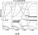
- FIGS. 4A-4Cband structures calculated using Density Functional Theory (DFT) are presented. It is well known in the art that DFT underestimates the absolute value of the bandgap. Hence all bands above the gap may be shifted by an appropriate "scissors correction.” However the shape of the band is known to be much more reliable. The vertical energy axes should be interpreted in this light.
- DFTDensity Functional Theory
- FIG. 4Ashows the calculated band structure from the gamma point (G) for both bulk silicon (represented by continuous lines) and for the 4/1 Si/O superlattice 25 shown in FIG. 1 (represented by dotted lines).
- the directionsrefer to the unit cell of the 4/1 Si/O structure and not to the conventional unit cell of Si, although the (001) direction in the figure does correspond to the (001) direction of the conventional unit cell of Si, and, hence, shows the expected location of the Si conduction band minimum.
- the (100) and (010) directions in the figurecorrespond to the (110) and (-110) directions of the conventional Si unit cell.
- the bands of Si on the figureare folded to represent them on the appropriate reciprocal lattice directions for the 4/1 Si/O structure.
- the conduction band minimum for the 4/1 Si/O structureis located at the gamma point in contrast to bulk silicon (Si), whereas the valence band minimum occurs at the edge of the Brillouin zone in the (001) direction which we refer to as the Z point.
- the greater curvature of the conduction band minimum for the 4/1 Si/O structurecompared to the curvature of the conduction band minimum for Si owing to the band splitting due to the perturbation introduced by the additional oxygen layer.
- FIG. 4Bshows the calculated band structure from the Z point for both bulk silicon (continuous lines) and for the 4/1 Si/O superlattice 25 (dotted lines). This figure illustrates the enhanced curvature of the valence band in the (100) direction.
- FIG. 4Cshows the calculated band structure from both the gamma and Z point for both bulk silicon (continuous lines) and for the 5/1/3/1 Si/O structure of the superlattice 25' of FIG. 3 (dotted lines). Due to the symmetry of the 5/1/3/1 Si/O structure, the calculated band structures in the (100) and (010) directions are equivalent. Thus the conductivity effective mass and mobility are expected to be isotropic in the plane parallel to the layers, i.e. perpendicular to the (001) stacking direction. Note that in the 5/1/3/1 Si/O example the conduction band minimum and the valence band maximum are both at or close to the Z point.
- the appropriate comparison and discriminationmay be made via the conductivity reciprocal effective mass tensor calculation. This leads Applicant to further theorize that the 5/1/3/1 superlattice 25' should be substantially direct bandgap. As will be understood by those skilled in the art, the appropriate matrix element for optical transition is another indicator of the distinction between direct and indirect bandgap behavior.
- tunneling diode structures and associated devicesincluding the above-described superlattice technology (also referred to as "MST" herein) are now described.
- resonant tunneling diodesoperate in a similar fashion to p-n junction diodes, in that the diode will conduct an "on" current with forward bias. Yet, in p-n junction diodes the bias current monotonically increases the forward current, whereas a resonant tunneling diode (RTD) exhibits negative differential resistance (NDR), in which the current level drops with increased bias. NDR characteristics increase operation points on load lines, and it is thus attractive for various circuit applications.
- doping levelsmay be at least 10x 18 /cm 3 , and levels of greater than 1x10 20 /cm 3 may be desired for lower contact resistance.
- RTDsalso typically use a relatively low doping level in the three regions immediately adjacent to and between the double barriers to prevent impurity scattering.
- the requisite doping levelis generally determined based upon the electron mean free path vs. the dimensions of the double barrier and tunneling layer thicknesses.
- the doping levelmay be set at approximately 1x10 16 /cm 3 .
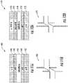
- N-type and P-type MST double barrier (DB) RTD structures 110, 110 and their associated band diagrams 101, 102are shown in FIGS. 5A, 6B and 5B, 6B , respectively.
- the N-type DBRTD structure 100illustratively includes a stack of layers including (starting from the bottom) a bottom n+ Si contact layer 102, a first superlattice barrier layer 103 (such as the superlattice layers 25, 25' described above - labeled MST in the drawings), an undoped (intrinsic) Si layer 104, a second superlattice barrier layer 105, and an upper n+ Si contact layer 106.
- the P-type DBRTD 110illustratively includes a stack of layers including (starting from the bottom) a bottom p+ Si contact layer 112, a first superlattice barrier layer 113, an undoped (intrinsic) Si layer 114, a second superlattice barrier layer 115, and an upper p+ Si contact layer 116.
- the superlattice barrier layers 103, 105 and 113, 115advantageously allow for the formation of potential barriers in the Si conduction band (CB) and valence band (VB) while maintaining Si epitaxy when forming the upper contact layers 106, 116. That is, the above-described superlattice structure advantageously allows semiconductor (e.g., silicon) bonds to propagate through the intervening oxygen atoms so that the epitaxy is not disrupted, allowing single crystalline semiconductor contact layers to be formed on top of the second superlattice barrier layers 105, 115.
- semiconductore.g., silicon
- the barrier heightmay advantageously be tuned for the given RTD application using the different structures and fabrication techniques described above. Simulations of a 4/1 repeating structure with a 15 ⁇ spacing between non-semiconductor (e.g., oxygen) monolayers projects approximately 0.6 eV for both the CB and VB. Furthermore, the potential barrier strength resulting from the MST barrier layers may be tuned based upon the oxygen concentration per monolayer, spacing between oxygen monolayers, and the number of oxygen monolayers used, for example, as will be appreciated by those skilled in the art.
- non-semiconductore.g., oxygen
- the superlattice filmmay advantageously be used to block dopant diffusion from the highly doped contact layers 102, 106 and 112, 116 into the undoped/intrinsic layers 104, 114, as discussed further above. That is, the superlattice material advantageously allows the desired doping profiles to be created for an RTD structure, with a high concentration of doping near the contacts and little or no doping in RTD regions, with relatively precise process control. Moreover, the superlattice material also provides for strain buffer capability for hetero epitaxial film growth, as well as a strain buffer effect for lattice mismatch of hetero epitaxial films.
- N-type and P-type DBRTD structures 120, 130are shown along with their respective band diagrams 121, 131.
- the DBRTD structures 120, 130illustratively include upper SiO 2 barrier layers 125, 135 instead of upper superlattice barrier layers.
- the N-type DBRTD 120illustratively includes (starting from the bottom of the stack) a bottom n+ Si contact layer 122, a superlattice barrier layer 123, an undoped (intrinsic) Si layer 124, the SiO 2 upper barrier layer 125, and an upper n+ polysilicon contact layer 126.
- the P-type DBRTD 130illustratively includes (starting from the bottom of the stack) a bottom p+ Si contact layer 132, an superlattice barrier layer 133, an undoped (intrinsic) Si layer 134, an SiO 2 barrier layer 135, and an upper p+ polysilicon contact layer 136.
- the SiO 2 layers 125, 135may be formed in a similar fashion to the way in which oxygen monolayers are formed during the MST monolayer deposition, but with a longer exposure time and/or higher dosage so that more Si bonding sites are populated with O atoms to form SiO 2 .
- the upper n+ and p+ Si contact layers 126, 136are polysilicon because they are formed on SiO 2 , as opposed to the single crystal Si layers 106, 116 which may be epitaxially grown on the superlattice layers 105, 115, as described above.
- example P-type DBRTD structures 140, 150are now described which are respectively similar to the P-type structures 110 and 130 shown in FIGS. 6A and 8A , with the exception of a Ge tunneling layer 144, 154 in place of the undoped (intrinsic) Si layers 114, 134 in the previous embodiments. Integration of thin Ge film into Si advantageously allows for a VB offset for appropriate applications.
- the P-type DBRTD 140illustratively includes (starting from the bottom of the stack) a bottom p+ Si contact layer 142, a first superlattice barrier layer 143, an undoped (intrinsic) Ge tunneling layer 144, a second superlattice barrier layer 145, and an upper p+ Si contact layer 146.
- the P-type DBRTD 150illustratively includes (starting from the bottom of the stack) a bottom p+ Si contact layer 152, a superlattice barrier layer 153, an undoped (intrinsic) Ge layer 154, an SiO 2 layer 155, and an upper p+ polysilicon Si contact layer 156. These same structures may instead be formed with n+ contact layers as well, as will be appreciated by those skilled in the art.
- FIGS. 11A-13Bthree examples of resonant inter-band tunneling diodes (RITDs) 160, 170, 180 are shown along with their respective band diagrams 161, 171, 181, which respectively have layer structures similar to those shown in FIGS. 5A , 7A , and 9A , with the difference being that the upper and lower contact layers in the current examples are oppositely doped (i.e., doped with opposite conductivity type dopants).
- RITDsresonant inter-band tunneling diodes
- the diode 160illustratively includes (starting from the bottom of the stack) a bottom p+ Si contact layer 162, a first superlattice barrier layer 163, an undoped (intrinsic) Si layer 164, a second superlattice barrier layer 165, and an n+ Si upper contact layer 166.
- the diode 170illustratively includes (starting from the bottom of the stack) a bottom p+ Si contact layer 172, an superlattice barrier layer 173, an undoped (intrinsic) Si layer 174, a SiO 2 barrier layer 175, and an upper n+ polysilicon contact layer 176.
- the third exampleillustratively includes (starting from the bottom of the stack) a bottom p+ Si contact layer 182, a first superlattice barrier layer 183, an undoped (intrinsic) Ge layer 184, a second superlattice barrier layer 185, and an n+ Si upper contact layer 186.
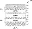
- FIGS. 14-16three example RTD structures 190, 210, and 230 according to the present invention are provided which are respectively similar to the three examples shown in FIGS. 5A , 9A and 10A , but which further include additional electron mean free path control layers.
- the first exampleis an N-type RTD illustratively including (starting at the bottom of the stack) an n+ Si contact layer 191, a first superlattice layer 192, a first undoped Si layer 193, a second superlattice layer 194, a second undoped Si layer 195, a third superlattice layer 196, a third undoped Si layer 197, a fourth superlattice layer 198, and an upper n+ Si contact layer 199 (note that this structure may have p+ contact layers as well in different embodiments).
- the superlattice layers 194, 196serve as potential barrier layers, and the pairs of layers 192/193 and 197/198 respectively define electron mean free path control layers 200, 201.
- the second exampleis a P-type RTD 210 illustratively including (starting from the bottom of the stack) a bottom p+ Si contact layer 211, a first superlattice layer 212, a first undoped Si layer 213, a second superlattice layer 214, an undoped Ge (or SiGe) layer 215, a third superlattice layer 216, a second undoped Si layer 217, a fourth superlattice layer 218, and an upper p+ contact layer 219 (note that this structure may have N-type contact layers in different embodiments).
- the superlattice layers 214, 216serve as potential barrier layers, and the pairs of layers 212/213 and 217/218 respectively define electron mean free path control layers 220, 221.
- the third exampleis an RITD 230 which illustratively includes (starting from the bottom of the stack) a p+ Si bottom contact layer 231, a first superlattice layer 232, a first undoped Si layer 233, a second superlattice layer 234, a second undoped Si layer 235, a third superlattice layer 236, a third undoped Si layer 237, a fourth superlattice layer 238, and an upper n+ Si contact layer 239 (note that the conductivities of the bottom and upper contact layers may be reversed in other embodiments).
- the superlattice layers 234, 236serve as potential barrier layers, and the pairs of layers 232/233 and 237/238 respectively define electron mean free path control layers 240, 241.
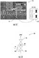
- FIG. 17one example application for replacing at least a portion of a tungsten (W) plug 271 in a CMOS FINFET device 270 with one or more of RTD structures 272 such as those described above is shown. It should be noted that RTD structure(s) 272 may be used in planar semiconductor devices as well.
- a MOBILE deviceillustratively includes a DBRTD or RTD 281 as described above and a second diode 282 (which may also be a DBRTD or RTD as described above in some embodiments) coupled in series between a clock signal Clock and ground. Furthermore, a transistor 283 has its source and drain coupled to the first and second contacts of the diode 282, and its gate coupled to an input signal IN. An output signal OUT is provided at the point where the diodes 281, 282 are coupled together.
- CMOS process flowin which a superlattice RTD module may be included to form the above-described superlattice RTD structures within CMOS devices is shown in the flow diagram 290 of FIG. 19 .
- the processbegins with a shallow trench isolation (STI) module 291, followed by a well module 292, a gate module 293, a lightly doped drain (LDD) module 294, a spacer and source/drain module 295, a silicide module 296, a contact/M1 module 297, and a back end of line (BEOL) module 298.
- STIshallow trench isolation
- LDDlightly doped drain
- the DBRTD formationoccurs within the silicide module 296, in that after an oxide chemical vapor deposition (CVD), the MST RTD module is inserted, which includes another (optional) oxide CVD, chemical mechanical polishing (CMP), RTD contact patterning, and superlattice RTD epitaxy to create the desired RTD device (which may be done in either a blanket form across an entire wafer (MST1) or selectively at different locations on the water (MST2) with an optional CMP).
- CVDoxide chemical vapor deposition
- CMPchemical mechanical polishing
- RTD contact patterningRTD contact patterning
- superlattice RTD epitaxyto create the desired RTD device (which may be done in either a blanket form across an entire wafer (MST1) or selectively at different locations on the water (MST2) with an optional CMP).
- the silicide module 296further illustratively includes silicide block mask patterning which includes lithography, etching, and photoresist (PR) removal, then silicide metal physical vapor deposition (PVD) including a pre-clean and sputter, followed by silicide rapid thermal anneal(s) (RTA), and metal removal via wet etch, for example.
- silicide block mask patterningwhich includes lithography, etching, and photoresist (PR) removal
- PVDsilicide metal physical vapor deposition
- RTAsilicide rapid thermal anneal
- Various devicesmay be created using the above-described structures and processes.
- One such deviceis a tunneling-based SRAM (TSRAM) cell.
- TSRAMtunneling-based SRAM
- a smaller than conventional 6T-SRAM cell⁇ 150F 2
- conventional DRAM cells4 ⁇ 8F 2
- Applicability to multi-bit cellsmay be provided by increasing the number of RTDs, for example.
- RTDs and DBRTDsmay be implemented in various logic circuit elements in which the above-described RTDs and DBRTDs may be implemented.
- One potential benefit of such configurationsmay include high-speed operation, as tunneling time scale is within pico seconds.
- Another potential benefitis relatively low power operation, because transition currents during state change may be limited by valley current. For example, greater than 50% reduction of circuit elements may be realized in some instances for implementing a given function, and the I-V curve of NDR devices intersects with other device's load line (at least) twice.
- RTDnot only compacts the memory and logic circuitry, but it may also add new functionality.
- integration of the DBRTD structures into standard Si CMOSmay help change future circuit design from a system level. For example, this may enable "neuron network" logic replacing conventional Boolean logic. Moreover, this may allow for an immediate impact by hybrid integration with conventional logic (pipelined ripple carry adder, as an example).
Landscapes
- Insulated Gate Type Field-Effect Transistor (AREA)
- Recrystallisation Techniques (AREA)
- Chemical & Material Sciences (AREA)
- Crystallography & Structural Chemistry (AREA)
- Engineering & Computer Science (AREA)
- Manufacturing & Machinery (AREA)
- Metal-Oxide And Bipolar Metal-Oxide Semiconductor Integrated Circuits (AREA)
Description
- The present disclosure generally relates to semiconductor devices and, more particularly, to semiconductor diode structures and related circuits and methods.
- Structures and techniques have been proposed to enhance the performance of semiconductor devices, such as by enhancing the mobility of the charge carriers. For example,
U.S. Patent Application No. 2003/0057416 to Currie et al. discloses strained material layers of silicon, silicon-germanium, and relaxed silicon and also including impurity-free zones that would otherwise cause performance degradation. The resulting biaxial strain in the upper silicon layer alters the carrier mobilities enabling higher speed and/or lower power devices. PublishedU.S. Patent Application No. 2003/0034529 to Fitzgerald et al. discloses a CMOS inverter also based upon similar strained silicon technology. U.S. Patent No. 6,472,685 B2 to Takagi discloses a semiconductor device including a silicon and carbon layer sandwiched between silicon layers so that the conduction band and valence band of the second silicon layer receive a tensile strain. Electrons having a smaller effective mass, and which have been induced by an electric field applied to the gate electrode, are confined in the second silicon layer, thus, an n-channel MOSFET is asserted to have a higher mobility.U.S. Patent No. 4,937,204 to Ishibashi et al. discloses a superlattice in which a plurality of layers, less than eight monolayers, and containing a fractional or binary or a binary compound semiconductor layer, are alternately and epitaxially grown. The direction of main current flow is perpendicular to the layers of the superlattice.U.S. Patent No. 5,357,119 to Wang et al. discloses a Si-Ge short period superlattice with higher mobility achieved by reducing alloy scattering in the superlattice. Along these lines,U.S. Patent No. 5,683,934 to Candelaria discloses an enhanced mobility MOSFET including a channel layer comprising an alloy of silicon and a second material substitutionally present in the silicon lattice at a percentage that places the channel layer under tensile stress.U.S. Patent No. 5,216,262 to Tsu discloses a quantum well structure comprising two barrier regions and a thin epitaxially grown semiconductor layer sandwiched between the barriers. Each barrier region consists of alternate layers of SiO2/Si with a thickness generally in a range of two to six monolayers. A much thicker section of silicon is sandwiched between the barriers.- An article entitled "Phenomena in silicon nanostructure devices" also to Tsu and published online September 6, 2000 by Applied Physics and Materials Science & Processing, pp. 391-402 discloses a semiconductor-atomic superlattice (SAS) of silicon and oxygen. The Si/O superlattice is disclosed as useful in a silicon quantum and light-emitting devices. In particular, a green electroluminescence diode structure was constructed and tested. Current flow in the diode structure is vertical, that is, perpendicular to the layers of the SAS. The disclosed SAS may include semiconductor layers separated by adsorbed species such as oxygen atoms, and CO molecules. The silicon growth beyond the adsorbed monolayer of oxygen is described as epitaxial with a fairly low defect density. One SAS structure included a 1.1 nm thick silicon portion that is about eight atomic layers of silicon, and another structure had twice this thickness of silicon. An article toLuo et al. entitled "Chemical Design of Direct-Gap Light-Emitting Silicon" published in Physical Review Letters, Vol. 89, No. 7 (August 12, 2002) further discusses the light emitting SAS structures of Tsu.
- Published International Application
WO 02/103,767 A1 to Wang - Published Great Britain Patent Application
2,347,520 to Mears et al. - characteristics. Other parameters, such as electrical conductivity, thermal conductivity and dielectric permittivity or magnetic permeability are disclosed as also possible to be designed into the material.
- Furthermore,
U.S. Pat. No. 6,376,337 to Wang et al. discloses a method for producing an insulating or barrier layer for semiconductor devices which includes depositing a layer of silicon and at least one additional element on the silicon substrate whereby the deposited layer is substantially free of defects such that epitaxial silicon substantially free of defects can be deposited on the deposited layer. Alternatively, a monolayer of one or more elements, preferably comprising oxygen, is absorbed on a silicon substrate. A plurality of insulating layers sandwiched between epitaxial silicon forms a barrier composite. US2008/073641A1 discloses structures include a tunneling device disposed over first and second lattice-mismatched semiconductor materials. Process embodiments include forming tunneling devices over lattice-mismatched materials.- Despite the existence of such approaches, further enhancements may be desirable for using advanced semiconductor materials and processing techniques to achieve improved performance in semiconductor devices.
- A semiconductor device including at least one resonant tunneling diode is provided. The at least one resonant tunneling diode includes a first doped semiconductor layer, and a first barrier layer on the first doped semiconductor layer The resonant tunneling diode further includes a first intrinsic semiconductor layer on the first barrier layer, a second barrier layer on the first intrinsic semiconductor layer, a second intrinsic semiconductor layer on the second barrier layer, a third barrier layer on the second intrinsic semiconductor layer, a third intrinsic semiconductor layer on the third barrier layer, a fourth barrier layer on the third intrinsic semiconductor layer, and a second doped semiconductor layer on the fourth barrier layer, characterised in that the first, second and third barrier layers comprise a superlattice, each superlattice comprising a plurality of stacked groups of layers, each group of layers comprising a plurality of stacked base semiconductor monolayers defining a base semiconductor portion, and at least one non-semiconductor monolayer constrained within a crystal lattice of adjacent base semiconductor portions, wherein constrained means that not all of the available semiconductor bonding sites of the opposing base semiconductor portions are populated with bonds to non-semiconductor atoms of the at least one non-semiconductor monolayer and that at least some atoms from opposing base semiconductor portions are chemically bound together, with the chemical bonds traversing the at least one intervening non-semiconductor monolayer therebetween.
- More particularly, the first and second doped semiconductor layers may comprise silicon, and the second intrinsic layer may comprise at least one of silicon and germanium in one example embodiment. Further, the second doped semiconductor layer may comprise a single crystal semiconductor layer.
- In accordance with one example embodiment, the first and second doped semiconductor layers may have the same dopant conductivity type. In accordance with another example, the first and second doped semiconductor layers may have opposite dopant conductivity types.
- Furthermore, the first barrier layer and the first intrinsic semiconductor layer may define a first electron mean free path control layer; and the third intrinsic semiconductor layer and the fourth barrier layer may define a second electron mean free path control layer. By way of example, the at least one non-semiconductor monolayer may comprise oxygen, and the semiconductor monolayers may comprise silicon.
- A method aspect is for making a semiconductor device and may include forming at least one double-barrier resonant tunneling diode by forming a first doped semiconductor layer, and forming a first barrier layer on the first doped semiconductor layer. The method further includes forming a first intrinsic semiconductor layer on the first barrier layer, forming a second barrier layer on the first intrinsic semiconductor layer, forming a second intrinsic semiconductor layer on the second barrier layer, forming a third barrier layer on the second intrinsic semiconductor layer, forming a third intrinsic semiconductor layer on the third barrier layer, forming a fourth barrier layer on the third intrinsic semiconductor layer, and forming a second doped semiconductor layer on the fourth barrier layer, characterised in that the first, second and third barrier layers comprise a superlattice, each superlattice comprising a plurality of stacked groups of layers, each group of layers comprising a plurality of stacked base semiconductor monolayers defining a base semiconductor portion, and at least one non-semiconductor monolayer constrained within a crystal lattice of adjacent base semiconductor portions, wherein constrained means that not all of the available semiconductor bonding sites of the opposing base semiconductor portions are populated with bonds to non-semiconductor atoms of the at least one non-semiconductor monolayer and that at least some atoms from opposing base semiconductor portions are chemically bound together, with the chemical bonds traversing the at least one intervening non-semiconductor monolayer therebetween.
- More particularly, the first and second doped semiconductor layers may comprise silicon, and the second intrinsic layer may comprise at least one of silicon and germanium in one example embodiments. Further, the second doped semiconductor layer may comprise a single crystal semiconductor layer.
- In accordance with one example embodiment, the first and second doped semiconductor layers may have the same dopant conductivity type. In accordance with another example, the first and second doped semiconductor layers may have opposite dopant conductivity types.
- Furthermore, the first barrier layer and the first intrinsic semiconductor layer may define a first electron mean free path control layer; and the third intrinsic semiconductor layer and the fourth barrier layer may define a second electron mean free path control layer. By way of example, the at least one non-semiconductor monolayer may comprise oxygen, and the semiconductor monolayers may comprise silicon.
FIG. 1 is a greatly enlarged schematic cross-sectional view of a superlattice for use in a semiconductor device in accordance with an example embodiment.FIG. 2 is a perspective schematic atomic diagram of a portion of the superlattice shown inFIG. 1 .FIG. 3 is a greatly enlarged schematic cross-sectional view of another embodiment of a superlattice in accordance with an example embodiment.FIG. 4A is a graph of the calculated band structure from the gamma point (G) for both bulk silicon as in the prior art, and for the 4/1 Si/O superlattice as shown inFIGS. 1-2 .FIG. 4B is a graph of the calculated band structure from the Z point for both bulk silicon as in the prior art, and for the 4/1 Si/O superlattice as shown inFIGS. 1-2 .FIG. 4C is a graph of the calculated band structure from both the gamma and Z points for both bulk silicon as in the prior art, and for the 5/1/3/1 Si/O superlattice as shown inFIG. 3 .FIG. 5A is a schematic cross-sectional diagram of an N-type double barrier resonant tunneling diode (DBRTD) including superlattice barrier layers in accordance with an example not forming part of the invention.FIG. 5B is an energy band diagram for the DBRTD ofFIG. 5A .FIG. 6A is a schematic cross-sectional diagram of a P-type double barrier resonant tunneling diode (DBRTD) including superlattice barrier layers in accordance with an example not forming part of the invention.FIG. 7A is a schematic cross-sectional diagram of an N-type DBRTD including superlattice and SiO2 barrier layers in accordance with an example not forming part of the invention.FIG. 7B is an energy band diagram for the DBRTD ofFIG. 7A .FIG. 8A is a schematic cross-sectional diagram of a P-type DBRTD including superlattice and SiO2 barrier layers in accordance with an example not forming part of the invention.FIG. 8B is an energy band diagram for the DBRTD ofFIG. 8A .FIG. 9A is a schematic cross-sectional diagram of a P-type DBRTD including superlattice barrier layers and a germanium intrinsic layer in accordance with an example not forming part of the invention.FIG. 9B is an energy band diagram for the DBRTD ofFIG. 9A .FIG. 10A is a schematic cross-sectional diagram of a P-type DBRTD including superlattice and SiO2 barrier layers and a germanium intrinsic layer in accordance with an example not forming part of the invention.FIG. 10B is an energy band diagram for the DBRTD ofFIG. 10A .FIG. 11A is a schematic cross-sectional diagram of an inter-band DBRTD including superlattice barrier layers and oppositely-doped contact layers in accordance with an example not forming part of the invention.FIG. 11B is an energy band diagram for the DBRTD ofFIG. 11A .FIG. 12A is a schematic cross-sectional diagram of an inter-band DBRTD including superlattice and SiO2 barrier layers and oppositely-doped contact layers in accordance with an example not forming part of the invention.FIG. 12B is an energy band diagram for the DBRTD ofFIG. 12A .FIG. 13A is a schematic cross-sectional diagram of an inter-band DBRTD including superlattice barrier layers and oppositely-doped contact layers with an intrinsic germanium layer in accordance with an example not forming part of the invention.FIG. 13B is an energy band diagram for the DBRTD ofFIG. 11A .FIG. 14 is a schematic cross-sectional diagram of an N-type RTD including superlattice barrier layers and electron mean free path control layers in accordance with an example embodiment of the present invention.FIG. 15 is a schematic cross-sectional diagram of a P-type RTD including superlattice barrier layers, an intrinsic germanium layer, and electron mean free path control layers in accordance with an example embodiment of the present invention.FIG. 16 is a schematic cross-sectional diagram of an inter-band RTD including superlattice barrier layers with oppositely doped contact layers and electron mean free path control layers in accordance with an example embodiment of the present invention.FIG. 17 is a cross-sectional diagram of a FINFET which may include one or more RTD devices in accordance with an example embodiment.FIG. 18 is schematic circuit diagram of a monostable-bistable transition logic element (MOBILE) which may include a RTD in accordance with an example embodiment.FIG. 19 is a flow diagram illustrating a process flow for making a semiconductor device which may include one or more RTD structures in accordance with an example embodiment.- Example embodiments of the invention as well as examples not forming part of the invention will now be described more fully hereinafter with reference to the accompanying drawings, in which the example embodiments are shown. The embodiments may, however, be implemented in many different forms and should not be construed as limited to the specific examples set forth herein. Rather, these embodiments are provided so that this disclosure will be thorough and complete. Like numbers refer to like elements throughout, and prime notation is used to indicate similar elements in different embodiments.
- Generally speaking, the present disclosure relates to tunneling diode devices, including RTD devices, having an enhanced semiconductor superlattice therein which may provide desired potential barrier and dopant confinement features and enabling integration of such devices in standard CMOS processes. The enhanced semiconductor superlattice is also referred to as an "MST" layer or "MST technology" in this disclosure and the accompanying Appendix A. Further background on the use of MST technology to provide dopant blocking features in semiconductor devices may be found in
U.S. Pat. No. 9,275,996 to Mears et al. - More particularly, the MST technology relates to advanced semiconductor materials such as the
superlattice 25 described further below. Applicant theorizes, without wishing to be bound thereto, that certain superlattices as described herein reduce the effective mass of charge carriers and that this thereby leads to higher charge carrier mobility. Effective mass is described with various definitions in the literature. As a measure of the improvement in effective mass Applicant's use a "conductivity reciprocal effective mass tensor",


- Applicant's definition of the conductivity reciprocal effective mass tensor is such that a tensorial component of the conductivity of the material is greater for greater values of the corresponding component of the conductivity reciprocal effective mass tensor. Again Applicant theorizes without wishing to be bound thereto that the superlattices described herein set the values of the conductivity reciprocal effective mass tensor so as to enhance the conductive properties of the material, such as typically for a preferred direction of charge carrier transport. The inverse of the appropriate tensor element is referred to as the conductivity effective mass. In other words, to characterize semiconductor material structures, the conductivity effective mass for electrons/holes as described above and calculated in the direction of intended carrier transport is used to distinguish improved materials.
- Applicant has identified improved materials or structures for use in semiconductor devices. More specifically, Applicant has identified materials or structures having energy band structures for which the appropriate conductivity effective masses for electrons and/or holes are substantially less than the corresponding values for silicon. In addition to the enhanced mobility characteristics of these structures, they may also be formed or used in such a manner that they provide piezoelectric, pyroelectric, and/or ferroelectric properties that are advantageous for use in a variety of different types of devices, as will be discussed further below.
- Referring now to
FIGS. 1 and2 , the materials or structures are in the form of asuperlattice 25 whose structure is controlled at the atomic or molecular level and may be formed using known techniques of atomic or molecular layer deposition. Thesuperlattice 25 includes a plurality oflayer groups 45a-45n arranged in stacked relation, as perhaps best understood with specific reference to the schematic cross-sectional view ofFIG. 1 . - Each group of
layers 45a-45n of thesuperlattice 25 illustratively includes a plurality of stackedbase semiconductor monolayers 46 defining a respective base semiconductor portion46a-46n and an energy band-modifyinglayer 50 thereon. The energy band-modifyinglayers 50 are indicated by stippling inFIG. 1 for clarity of illustration. - The energy band-modifying
layer 50 illustratively includes one non-semiconductor monolayer constrained within a crystal lattice of adjacent base semiconductor portions. By "constrained within a crystal lattice of adjacent base semiconductor portions" it is meant that at least some semiconductor atoms from opposing base semiconductor portions46a-46n are chemically bound together through thenon-semiconductor monolayer 50 therebetween, as seen inFIG. 2 . Generally speaking, this configuration is made possible by controlling the amount of non-semiconductor material that is deposited on semiconductor portions46a-46n through atomic layer deposition techniques so that not all (i.e., less than full or 100% coverage) of the available semiconductor bonding sites are populated with bonds to non-semiconductor atoms, as will be discussed further below. Thus, asfurther monolayers 46 of semiconductor material are deposited on or over anon-semiconductor monolayer 50, the newly deposited semiconductor atoms will populate the remaining vacant bonding sites of the semiconductor atoms below the non-semiconductor monolayer. - In other embodiments, more than one such non-semiconductor monolayer may be possible. It should be noted that reference herein to a non-semiconductor or semiconductor monolayer means that the material used for the monolayer would be a non-semiconductor or semiconductor if formed in bulk. That is, a single monolayer of a material, such as silicon, may not necessarily exhibit the same properties that it would if formed in bulk or in a relatively thick layer, as will be appreciated by those skilled in the art.
- Applicant theorizes without wishing to be bound thereto that energy band-modifying
layers 50 and adjacent base semiconductor portions46a-46n cause thesuperlattice 25 to have a lower appropriate conductivity effective mass for the charge carriers in the parallel layer direction than would otherwise be present. Considered another way, this parallel direction is orthogonal to the stacking direction. Theband modifying layers 50 may also cause thesuperlattice 25 to have a common energy band structure, while also advantageously functioning as an insulator between layers or regions vertically above and below the superlattice. - Moreover, this superlattice structure may also advantageously act as a barrier to dopant and/or material diffusion between layers vertically above and below the
superlattice 25. These properties may thus advantageously allow thesuperlattice 25 to provide an interface for high-K dielectrics which not only reduces diffusion of the high-K material into the channel region, but which may also advantageously reduce unwanted scattering effects and improve device mobility, as will be appreciated by those skilled in the art. - It is also theorized that semiconductor devices including the
superlattice 25 may enjoy a higher charge carrier mobility based upon the lower conductivity effective mass than would otherwise be present. In some embodiments, and as a result of the band engineering achieved by the present invention, thesuperlattice 25 may further have a substantially direct energy bandgap that may be particularly advantageous for opto-electronic devices, for example. - The
superlattice 25 also illustratively includes acap layer 52 on anupper layer group 45n. Thecap layer 52 may comprise a plurality ofbase semiconductor monolayers 46. Thecap layer 52 may have between 2 to 100 monolayers of the base semiconductor, and, more preferably between 10 to 50 monolayers. - Each base semiconductor portion46a-46n may comprise a base semiconductor selected from the group consisting of Group IV semiconductors, Group III-V semiconductors, and Group II-VI semiconductors. Of course, the term Group IV semiconductors also includes Group IV-IV semiconductors, as will be appreciated by those skilled in the art. More particularly, the base semiconductor may comprise at least one of silicon and germanium, for example.
- Each energy band-modifying
layer 50 may comprise a non-semiconductor selected from the group consisting of oxygen, nitrogen, fluorine, carbon and carbon-oxygen, for example. The non-semiconductor is also desirably thermally stable through deposition of a next layer to thereby facilitate manufacturing. In other embodiments, the non-semiconductor may be another inorganic or organic element or compound that is compatible with the given semiconductor processing as will be appreciated by those skilled in the art. More particularly, the base semiconductor may comprise at least one of silicon and germanium, for example - It should be noted that the term monolayer is meant to include a single atomic layer and also a single molecular layer. It is also noted that the energy band-modifying
layer 50 provided by a single monolayer is also meant to include a monolayer wherein not all of the possible sites are occupied (i.e., there is less than full or 100% coverage). For example, with particular reference to the atomic diagram ofFIG. 2 , a 4/1 repeating structure is illustrated for silicon as the base semiconductor material, and oxygen as the energy band-modifying material. Only half of the possible sites for oxygen are occupied in the illustrated example. - In other embodiments and/or with different materials this one-half occupation would not necessarily be the case as will be appreciated by those skilled in the art. Indeed it can be seen even in this schematic diagram, that individual atoms of oxygen in a given monolayer are not precisely aligned along a flat plane as will also be appreciated by those of skill in the art of atomic deposition. By way of example, a preferred occupation range is from about one-eighth to one-half of the possible oxygen sites being full, although other numbers may be used in certain embodiments.
- Silicon and oxygen are currently widely used in conventional semiconductor processing, and, hence, manufacturers will be readily able to use these materials as described herein. Atomic or monolayer deposition is also now widely used. Accordingly, semiconductor devices incorporating the
superlattice 25 in accordance with the invention may be readily adopted and implemented, as will be appreciated by those skilled in the art. - It is theorized without Applicant wishing to be bound thereto that for a superlattice, such as the Si/O superlattice, for example, that the number of silicon monolayers should desirably be seven or less so that the energy band of the superlattice is common or relatively uniform throughout to achieve the desired advantages. The 4/1 repeating structure shown in
FIGS. 1 and2 , for Si/O has been modeled to indicate an enhanced mobility for electrons and holes in the X direction. For example, the calculated conductivity effective mass for electrons (isotropic for bulk silicon) is 0.26 and for the 4/1 SiO superlattice in the X direction it is 0.12 resulting in a ratio of 0.46. Similarly, the calculation for holes yields values of 0.36 for bulk silicon and 0.16 for the 4/1 Si/O superlattice resulting in a ratio of 0.44. - While such a directionally preferential feature may be desired in certain semiconductor devices, other devices may benefit from a more uniform increase in mobility in any direction parallel to the groups of layers. It may also be beneficial to have an increased mobility for both electrons and holes, or just one of these types of charge carriers as will be appreciated by those skilled in the art.
- The lower conductivity effective mass for the 4/1 Si/O embodiment of the
superlattice 25 may be less than two-thirds the conductivity effective mass than would otherwise occur, and this applies for both electrons and holes. Of course, thesuperlattice 25 may further comprise at least one type of conductivity dopant therein, as will also be appreciated by those skilled in the art. - Indeed, referring now additionally to
FIG. 3 , another embodiment of a superlattice25' in accordance with the invention having different properties is now described. In this embodiment, a repeating pattern of 3/1/5/1 is illustrated. More particularly, the lowest base semiconductor portion46a' has three monolayers, and the second lowestbase semiconductor portion 46b' has five monolayers. This pattern repeats throughout the superlattice25'. The energy band-modifying layers50' may each include a single monolayer. For such a superlattice25' including Si/O, the enhancement of charge carrier mobility is independent of orientation in the plane of the layers. Those other elements ofFIG. 3 not specifically mentioned are similar to those discussed above with reference toFIG. 1 and need no further discussion herein. - In some device embodiments, all of the base semiconductor portions of a superlattice may be a same number of monolayers thick. In other embodiments, at least some of the base semiconductor portions may be a different number of monolayers thick. In still other embodiments, all of the base semiconductor portions may be a different number of monolayers thick.
- In
FIGS. 4A-4C , band structures calculated using Density Functional Theory (DFT) are presented. It is well known in the art that DFT underestimates the absolute value of the bandgap. Hence all bands above the gap may be shifted by an appropriate "scissors correction." However the shape of the band is known to be much more reliable. The vertical energy axes should be interpreted in this light. FIG. 4A shows the calculated band structure from the gamma point (G) for both bulk silicon (represented by continuous lines) and for the 4/1 Si/O superlattice 25 shown inFIG. 1 (represented by dotted lines). The directions refer to the unit cell of the 4/1 Si/O structure and not to the conventional unit cell of Si, although the (001) direction in the figure does correspond to the (001) direction of the conventional unit cell of Si, and, hence, shows the expected location of the Si conduction band minimum. The (100) and (010) directions in the figure correspond to the (110) and (-110) directions of the conventional Si unit cell. Those skilled in the art will appreciate that the bands of Si on the figure are folded to represent them on the appropriate reciprocal lattice directions for the 4/1 Si/O structure.- It can be seen that the conduction band minimum for the 4/1 Si/O structure is located at the gamma point in contrast to bulk silicon (Si), whereas the valence band minimum occurs at the edge of the Brillouin zone in the (001) direction which we refer to as the Z point. One may also note the greater curvature of the conduction band minimum for the 4/1 Si/O structure compared to the curvature of the conduction band minimum for Si owing to the band splitting due to the perturbation introduced by the additional oxygen layer.
FIG. 4B shows the calculated band structure from the Z point for both bulk silicon (continuous lines) and for the 4/1 Si/O superlattice25 (dotted lines). This figure illustrates the enhanced curvature of the valence band in the (100) direction.FIG. 4C shows the calculated band structure from both the gamma and Z point for both bulk silicon (continuous lines) and for the 5/1/3/1 Si/O structure of the superlattice25' ofFIG. 3 (dotted lines). Due to the symmetry of the 5/1/3/1 Si/O structure, the calculated band structures in the (100) and (010) directions are equivalent. Thus the conductivity effective mass and mobility are expected to be isotropic in the plane parallel to the layers, i.e. perpendicular to the (001) stacking direction. Note that in the 5/1/3/1 Si/O example the conduction band minimum and the valence band maximum are both at or close to the Z point.- Although increased curvature is an indication of reduced effective mass, the appropriate comparison and discrimination may be made via the conductivity reciprocal effective mass tensor calculation. This leads Applicant to further theorize that the 5/1/3/1 superlattice25' should be substantially direct bandgap. As will be understood by those skilled in the art, the appropriate matrix element for optical transition is another indicator of the distinction between direct and indirect bandgap behavior.
- Turning to
FIGS. 5A-6B , tunneling diode structures and associated devices including the above-described superlattice technology (also referred to as "MST" herein) are now described. By way of background, resonant tunneling diodes operate in a similar fashion to p-n junction diodes, in that the diode will conduct an "on" current with forward bias. Yet, in p-n junction diodes the bias current monotonically increases the forward current, whereas a resonant tunneling diode (RTD) exhibits negative differential resistance (NDR), in which the current level drops with increased bias. NDR characteristics increase operation points on load lines, and it is thus attractive for various circuit applications. - Generally speaking, most RTD devices utilize III-V materials, which makes integration into Si-based CMOS platforms very difficult. Moreover, a high doping level is typically desired at the contact regions for ohmic contacts. For example, doping levels may be at least 10x18/cm3, and levels of greater than 1x10²⁰/cm3 may be desired for lower contact resistance.
- On the other hand, RTDs also typically use a relatively low doping level in the three regions immediately adjacent to and between the double barriers to prevent impurity scattering. The requisite doping level is generally determined based upon the electron mean free path vs. the dimensions of the double barrier and tunneling layer thicknesses. Typically, the doping level may be set at approximately 1x10¹⁶/cm3.
- N-type and P-type MST double barrier (DB)
RTD structures FIGS. 5A, 6B and 5B, 6B , respectively. The N-type DBRTD structure 100 illustratively includes a stack of layers including (starting from the bottom) a bottom n+Si contact layer 102, a first superlattice barrier layer103 (such as the superlattice layers25, 25' described above - labeled MST in the drawings), an undoped (intrinsic)Si layer 104, a secondsuperlattice barrier layer 105, and an upper n+Si contact layer 106. Similarly, the P-type DBRTD 110 illustratively includes a stack of layers including (starting from the bottom) a bottom p+Si contact layer 112, a firstsuperlattice barrier layer 113, an undoped (intrinsic)Si layer 114, a secondsuperlattice barrier layer 115, and an upper p+Si contact layer 116. - The superlattice barrier layers103, 105 and113, 115 advantageously allow for the formation of potential barriers in the Si conduction band (CB) and valence band (VB) while maintaining Si epitaxy when forming the upper contact layers106, 116. That is, the above-described superlattice structure advantageously allows semiconductor (e.g., silicon) bonds to propagate through the intervening oxygen atoms so that the epitaxy is not disrupted, allowing single crystalline semiconductor contact layers to be formed on top of the second superlattice barrier layers105, 115.
- The barrier height may advantageously be tuned for the given RTD application using the different structures and fabrication techniques described above. Simulations of a 4/1 repeating structure with a 15Å spacing between non-semiconductor (e.g., oxygen) monolayers projects approximately 0.6 eV for both the CB and VB. Furthermore, the potential barrier strength resulting from the MST barrier layers may be tuned based upon the oxygen concentration per monolayer, spacing between oxygen monolayers, and the number of oxygen monolayers used, for example, as will be appreciated by those skilled in the art.
- However, another important characteristic of the superlattice film is that it may advantageously be used to block dopant diffusion from the highly doped contact layers102, 106 and112, 116 into the undoped/
intrinsic layers - Referring additionally to
FIGS. 7A-8B , other examples of N-type and P-type DBRTD structures DBRTD structures DBRTD structures type DBRTD 120 illustratively includes (starting from the bottom of the stack) a bottom n+Si contact layer 122, asuperlattice barrier layer 123, an undoped (intrinsic)Si layer 124, the SiO2upper barrier layer 125, and an upper n+polysilicon contact layer 126. Similarly, the P-type DBRTD 130 illustratively includes (starting from the bottom of the stack) a bottom p+Si contact layer 132, ansuperlattice barrier layer 133, an undoped (intrinsic)Si layer 134, an SiO2 barrier layer135, and an upper p+polysilicon contact layer 136. The SiO2 layers125, 135 may be formed in a similar fashion to the way in which oxygen monolayers are formed during the MST monolayer deposition, but with a longer exposure time and/or higher dosage so that more Si bonding sites are populated with O atoms to form SiO2. In these examples, the upper n+ and p+ Si contact layers126, 136 are polysilicon because they are formed on SiO2, as opposed to the single crystal Si layers106, 116 which may be epitaxially grown on the superlattice layers105, 115, as described above. - Turning to
FIGS. 9A-10B , example P-type DBRTD structures type structures FIGS. 6A and8A , with the exception of aGe tunneling layer layers - The P-
type DBRTD 140 illustratively includes (starting from the bottom of the stack) a bottom p+Si contact layer 142, a firstsuperlattice barrier layer 143, an undoped (intrinsic)Ge tunneling layer 144, a secondsuperlattice barrier layer 145, and an upper p+Si contact layer 146. In the second example, the P-type DBRTD 150 illustratively includes (starting from the bottom of the stack) a bottom p+Si contact layer 152, asuperlattice barrier layer 153, an undoped (intrinsic)Ge layer 154, an SiO2 layer155, and an upper p+ polysiliconSi contact layer 156. These same structures may instead be formed with n+ contact layers as well, as will be appreciated by those skilled in the art. - Turning now to
FIGS. 11A-13B , three examples of resonant inter-band tunneling diodes (RITDs)160, 170, 180 are shown along with their respective band diagrams161, 171, 181, which respectively have layer structures similar to those shown inFIGS. 5A ,7A , and9A , with the difference being that the upper and lower contact layers in the current examples are oppositely doped (i.e., doped with opposite conductivity type dopants). More particularly, in the first example the diode160 illustratively includes (starting from the bottom of the stack) a bottom p+Si contact layer 162, a firstsuperlattice barrier layer 163, an undoped (intrinsic)Si layer 164, a secondsuperlattice barrier layer 165, and an n+ Si upper contact layer166. In the second example, thediode 170 illustratively includes (starting from the bottom of the stack) a bottom p+Si contact layer 172, ansuperlattice barrier layer 173, an undoped (intrinsic)Si layer 174, a SiO2 barrier layer175, and an upper n+polysilicon contact layer 176. The third example illustratively includes (starting from the bottom of the stack) a bottom p+Si contact layer 182, a firstsuperlattice barrier layer 183, an undoped (intrinsic)Ge layer 184, a secondsuperlattice barrier layer 185, and an n+ Siupper contact layer 186. - Turning now to
FIGS. 14-16 , threeexample RTD structures FIGS. 5A ,9A and 10A , but which further include additional electron mean free path control layers. More particularly, the first example is an N-type RTD illustratively including (starting at the bottom of the stack) an n+Si contact layer 191, afirst superlattice layer 192, a firstundoped Si layer 193, asecond superlattice layer 194, a secondundoped Si layer 195, athird superlattice layer 196, a thirdundoped Si layer 197, afourth superlattice layer 198, and an upper n+ Si contact layer199 (note that this structure may have p+ contact layers as well in different embodiments). The superlattice layers194, 196 serve as potential barrier layers, and the pairs oflayers 192/193 and197/198 respectively define electron mean free path control layers200, 201. - The second example is a P-
type RTD 210 illustratively including (starting from the bottom of the stack) a bottom p+Si contact layer 211, afirst superlattice layer 212, a firstundoped Si layer 213, asecond superlattice layer 214, an undoped Ge (or SiGe)layer 215, athird superlattice layer 216, a secondundoped Si layer 217, afourth superlattice layer 218, and an upper p+ contact layer219 (note that this structure may have N-type contact layers in different embodiments). The superlattice layers214, 216 serve as potential barrier layers, and the pairs oflayers 212/213 and217/218 respectively define electron mean free path control layers220, 221. - The third example is an
RITD 230 which illustratively includes (starting from the bottom of the stack) a p+ Sibottom contact layer 231, afirst superlattice layer 232, a firstundoped Si layer 233, asecond superlattice layer 234, a secondundoped Si layer 235, athird superlattice layer 236, a thirdundoped Si layer 237, afourth superlattice layer 238, and an upper n+ Si contact layer239 (note that the conductivities of the bottom and upper contact layers may be reversed in other embodiments). The superlattice layers234, 236 serve as potential barrier layers, and the pairs oflayers 232/233 and237/238 respectively define electron mean free path control layers240, 241. - Turning now to
FIG. 17 , one example application for replacing at least a portion of a tungsten (W) plug271 in aCMOS FINFET device 270 with one or more ofRTD structures 272 such as those described above is shown. It should be noted that RTD structure(s)272 may be used in planar semiconductor devices as well. - Referring to
FIG. 18 , a MOBILE device illustratively includes a DBRTD orRTD 281 as described above and a second diode282 (which may also be a DBRTD or RTD as described above in some embodiments) coupled in series between a clock signal Clock and ground. Furthermore, atransistor 283 has its source and drain coupled to the first and second contacts of thediode 282, and its gate coupled to an input signal IN. An output signal OUT is provided at the point where thediodes - An example CMOS process flow in which a superlattice RTD module may be included to form the above-described superlattice RTD structures within CMOS devices is shown in the flow diagram290 of
FIG. 19 . The process begins with a shallow trench isolation (STI)module 291, followed by awell module 292, agate module 293, a lightly doped drain (LDD)module 294, a spacer and source/drain module 295, asilicide module 296, a contact/M1 module 297, and a back end of line (BEOL)module 298. More particularly, in the illustrated example, the DBRTD formation occurs within thesilicide module 296, in that after an oxide chemical vapor deposition (CVD), the MST RTD module is inserted, which includes another (optional) oxide CVD, chemical mechanical polishing (CMP), RTD contact patterning, and superlattice RTD epitaxy to create the desired RTD device (which may be done in either a blanket form across an entire wafer (MST1) or selectively at different locations on the water (MST2) with an optional CMP). Thesilicide module 296 further illustratively includes silicide block mask patterning which includes lithography, etching, and photoresist (PR) removal, then silicide metal physical vapor deposition (PVD) including a pre-clean and sputter, followed by silicide rapid thermal anneal(s) (RTA), and metal removal via wet etch, for example. It should be noted that certain steps and modules may be performed in different orders in different embodiments, depending upon the type of semiconductor device being created. - Various devices may be created using the above-described structures and processes. One such device is a tunneling-based SRAM (TSRAM) cell. Using the above-described techniques, a smaller than conventional 6T-SRAM cell (∼150F2) may be produced having less power consumption than conventional DRAM cells (4∼8F2). Applicability to multi-bit cells may be provided by increasing the number of RTDs, for example.
- Other logic circuit elements in which the above-described RTDs and DBRTDs may be implemented include FETs and BJTs. One potential benefit of such configurations may include high-speed operation, as tunneling time scale is within pico seconds. Another potential benefit is relatively low power operation, because transition currents during state change may be limited by valley current. For example, greater than 50% reduction of circuit elements may be realized in some instances for implementing a given function, and the I-V curve of NDR devices intersects with other device's load line (at least) twice.
- As noted above, another advantageous application for the RTDs and DBRTDs described herein is a MOBILE logic element. The RTD not only compacts the memory and logic circuitry, but it may also add new functionality. Moreover, integration of the DBRTD structures into standard Si CMOS may help change future circuit design from a system level. For example, this may enable "neuron network" logic replacing conventional Boolean logic. Moreover, this may allow for an immediate impact by hybrid integration with conventional logic (pipelined ripple carry adder, as an example).
- Many modifications and other embodiments of the invention will come to the mind of one skilled in the art having the benefit of the teachings presented in the foregoing descriptions and the associated drawings. Therefore, it is understood that the invention is not to be limited to the specific embodiments disclosed, and that modifications and embodiments are intended to be included within the scope of the appended claims.


Claims (15)
- A semiconductor device comprising:
at least one resonant tunneling diode (190) comprising
a first doped semiconductor layer (191),
a first barrier layer (192) on the first doped semiconductor layer,
a first intrinsic semiconductor layer (193) on the first barrier layer,
a second barrier layer (194) on the first intrinsic semiconductor layer,
a second intrinsic semiconductor layer (195) on the second barrier layer,
a third barrier layer (196) on the second intrinsic semiconductor layer,
a third intrinsic semiconductor layer (197) on the third barrier layer,
a fourth barrier layer (198) on the third intrinsic semiconductor layer, and
a second doped semiconductor layer (199) on the fourth barrier layer,
characterised in that the first, second and third barrier layers comprise a superlattice, each superlattice comprising a plurality of stacked groups of layers (45a-45n), each group of layers comprising a plurality of stacked base semiconductor monolayers (46) defining a base semiconductor portion (46a-46n), and at least one non-semiconductor monolayer (50) constrained within a crystal lattice of adjacent base semiconductor portions, wherein constrained means that not all of the available semiconductor bonding sites of the opposing base semiconductor portions are populated with bonds to non-semiconductor atoms of the at least one non-semiconductor monolayer and that at least some atoms from opposing base semiconductor portions are chemically bound together, with the chemical bonds traversing the at least one intervening non-semiconductor monolayer therebetween. - The semiconductor device of Claim 1 wherein the first and second doped semiconductor layers each comprises silicon, and wherein the second intrinsic layer comprises at least one of silicon and germanium.
- The semiconductor device of Claim 1 wherein the fourth barrier layer also comprises a superlattice having the same structure as the superlattice of the first barrier layer.
- The semiconductor device of Claim 1 wherein the second doped semiconductor layer comprises a single crystal semiconductor layer.
- The semiconductor device of Claim 1 wherein the first and second doped semiconductor layers have a same dopant conductivity type.
- The semiconductor device of Claim 1 wherein the first and second doped semiconductor layers have opposite dopant conductivity types.
- The semiconductor device of Claim 1 wherein the first barrier layer and the first intrinsic semiconductor layer define an electron mean free path control layer.
- The semiconductor device of Claim 1 wherein the third intrinsic semiconductor layer and the fourth barrier layer define an electron mean free path control layer.
- The semiconductor device of Claim 1 wherein the at least one non-semiconductor monolayer comprises oxygen.
- The semiconductor device of Claim 1 wherein the semiconductor monolayers comprise silicon.
- A method for making a semiconductor device comprising:
forming at least one resonant tunneling diode (190) by
forming a first doped semiconductor layer (191),
forming a first barrier layer (192) on the first doped semiconductor layer,
forming a first intrinsic semiconductor layer (193) on the first barrier layer,
forming a second barrier layer (194) on the first intrinsic semiconductor layer,
forming a second intrinsic semiconductor layer (195) on the second barrier layer,
forming a third barrier layer (196) on the second intrinsic semiconductor layer,
forming a third intrinsic semiconductor layer (197) on the third barrier layer,
forming a fourth barrier layer (198) on the third intrinsic semiconductor layer, and
forming a second doped semiconductor layer (199) on the fourth barrier layer,
characterised in that the first, second and third barrier layers comprise a superlattice, each superlattice comprising a plurality of stacked groups of layers (45a-45n), each group of layers comprising a plurality of stacked base semiconductor monolayers (46) defining a base semiconductor portion (46a-46n), and at least one non-semiconductor monolayer (50) constrained within a crystal lattice of adjacent base semiconductor portions, wherein constrained means that not all of the available semiconductor bonding sites of the opposing base semiconductor portions are populated with bonds to non-semiconductor atoms of the at least one non-semiconductor monolayer and that at least some atoms from opposing base semiconductor portions are chemically bound together, with the chemical bonds traversing the at least one intervening non-semiconductor monolayer therebetween. - The method of Claim 11 wherein the first and second doped semiconductor layers each comprises silicon, and wherein the second intrinsic layer comprises at least one of silicon and germanium.
- The method of Claim 11 wherein the fourth barrier layer also comprises a superlattice having the same structure as the superlattice of the first barrier layer.
- The method of Claim 13 wherein the second doped semiconductor layer comprises a single crystal semiconductor layer.
- The method of Claim 11 wherein the first and second doped semiconductor layers have a same dopant conductivity type.
Applications Claiming Priority (4)
| Application Number | Priority Date | Filing Date | Title |
|---|---|---|---|
| US201662371971P | 2016-08-08 | 2016-08-08 | |
| US15/670,266US10170603B2 (en) | 2016-08-08 | 2017-08-07 | Semiconductor device including a resonant tunneling diode structure with electron mean free path control layers |
| US15/670,274US10170604B2 (en) | 2016-08-08 | 2017-08-07 | Method for making a semiconductor device including a resonant tunneling diode with electron mean free path control layers |
| PCT/US2017/045863WO2018031527A1 (en) | 2016-08-08 | 2017-08-08 | Semiconductor device including a resonant tunneling diode structure with electron mean free path control layers comprising a superlattice and associated methods |
Publications (2)
| Publication Number | Publication Date |
|---|---|
| EP3497728A1 EP3497728A1 (en) | 2019-06-19 |
| EP3497728B1true EP3497728B1 (en) | 2021-05-26 |
Family
ID=61069628
Family Applications (2)
| Application Number | Title | Priority Date | Filing Date |
|---|---|---|---|
| EP17754917.7AActiveEP3497728B1 (en) | 2016-08-08 | 2017-08-08 | Semiconductor device including a resonant tunneling diode structure with electron mean free path control layers comprising a superlattice and associated methods |
| EP17754916.9AActiveEP3494599B1 (en) | 2016-08-08 | 2017-08-08 | Semiconductor device including resonant tunneling diode structure having a superlattice and related methods |
Family Applications After (1)
| Application Number | Title | Priority Date | Filing Date |
|---|---|---|---|
| EP17754916.9AActiveEP3494599B1 (en) | 2016-08-08 | 2017-08-08 | Semiconductor device including resonant tunneling diode structure having a superlattice and related methods |
Country Status (5)
| Country | Link |
|---|---|
| US (4) | US10170603B2 (en) |
| EP (2) | EP3497728B1 (en) |
| CN (2) | CN109791952B (en) |
| TW (3) | TWI648855B (en) |
| WO (2) | WO2018031522A1 (en) |
Families Citing this family (58)
| Publication number | Priority date | Publication date | Assignee | Title |
|---|---|---|---|---|
| US10381242B2 (en)* | 2017-05-16 | 2019-08-13 | Atomera Incorporated | Method for making a semiconductor device including a superlattice as a gettering layer |
| US10367064B2 (en) | 2017-06-13 | 2019-07-30 | Atomera Incorporated | Semiconductor device with recessed channel array transistor (RCAT) including a superlattice |
| WO2019036572A1 (en) | 2017-08-18 | 2019-02-21 | Atomera Incorporated | Semiconductor device and method including non-monocrystalline stringer adjacent a superlattice-sti interface |
| US10615209B2 (en)* | 2017-12-15 | 2020-04-07 | Atomera Incorporated | CMOS image sensor including stacked semiconductor chips and readout circuitry including a superlattice |
| CN111937119B (en) | 2018-03-08 | 2024-07-23 | 阿托梅拉公司 | Semiconductor device including enhanced contact structure with superlattice and related methods |
| US10468245B2 (en) | 2018-03-09 | 2019-11-05 | Atomera Incorporated | Semiconductor device including compound semiconductor materials and an impurity and point defect blocking superlattice |
| US10727049B2 (en) | 2018-03-09 | 2020-07-28 | Atomera Incorporated | Method for making a semiconductor device including compound semiconductor materials and an impurity and point defect blocking superlattice |
| US11664459B2 (en) | 2018-04-12 | 2023-05-30 | Atomera Incorporated | Method for making an inverted T channel field effect transistor (ITFET) including a superlattice |
| US11355667B2 (en) | 2018-04-12 | 2022-06-07 | Atomera Incorporated | Method for making semiconductor device including vertically integrated optical and electronic devices and comprising a superlattice |
| US10566191B1 (en) | 2018-08-30 | 2020-02-18 | Atomera Incorporated | Semiconductor device including superlattice structures with reduced defect densities |
| US10811498B2 (en) | 2018-08-30 | 2020-10-20 | Atomera Incorporated | Method for making superlattice structures with reduced defect densities |
| US20200135489A1 (en)* | 2018-10-31 | 2020-04-30 | Atomera Incorporated | Method for making a semiconductor device including a superlattice having nitrogen diffused therein |
| US10847618B2 (en) | 2018-11-16 | 2020-11-24 | Atomera Incorporated | Semiconductor device including body contact dopant diffusion blocking superlattice having reduced contact resistance |
| US10840336B2 (en) | 2018-11-16 | 2020-11-17 | Atomera Incorporated | Semiconductor device with metal-semiconductor contacts including oxygen insertion layer to constrain dopants and related methods |
| US10593761B1 (en)* | 2018-11-16 | 2020-03-17 | Atomera Incorporated | Method for making a semiconductor device having reduced contact resistance |
| US10854717B2 (en) | 2018-11-16 | 2020-12-01 | Atomera Incorporated | Method for making a FINFET including source and drain dopant diffusion blocking superlattices to reduce contact resistance |
| US10580867B1 (en) | 2018-11-16 | 2020-03-03 | Atomera Incorporated | FINFET including source and drain regions with dopant diffusion blocking superlattice layers to reduce contact resistance |
| US10818755B2 (en) | 2018-11-16 | 2020-10-27 | Atomera Incorporated | Method for making semiconductor device including source/drain dopant diffusion blocking superlattices to reduce contact resistance |
| US10840337B2 (en) | 2018-11-16 | 2020-11-17 | Atomera Incorporated | Method for making a FINFET having reduced contact resistance |
| US10580866B1 (en) | 2018-11-16 | 2020-03-03 | Atomera Incorporated | Semiconductor device including source/drain dopant diffusion blocking superlattices to reduce contact resistance |
| US10840335B2 (en) | 2018-11-16 | 2020-11-17 | Atomera Incorporated | Method for making semiconductor device including body contact dopant diffusion blocking superlattice to reduce contact resistance |
| US10916642B2 (en) | 2019-04-18 | 2021-02-09 | Globalfoundries U.S. Inc. | Heterojunction bipolar transistor with emitter base junction oxide interface |
| US11094818B2 (en) | 2019-04-23 | 2021-08-17 | Atomera Incorporated | Method for making a semiconductor device including a superlattice and an asymmetric channel and related methods |
| US10825902B1 (en) | 2019-07-17 | 2020-11-03 | Atomera Incorporated | Varactor with hyper-abrupt junction region including spaced-apart superlattices |
| US10937888B2 (en) | 2019-07-17 | 2021-03-02 | Atomera Incorporated | Method for making a varactor with a hyper-abrupt junction region including spaced-apart superlattices |
| US10879357B1 (en) | 2019-07-17 | 2020-12-29 | Atomera Incorporated | Method for making a semiconductor device having a hyper-abrupt junction region including a superlattice |
| US10868120B1 (en) | 2019-07-17 | 2020-12-15 | Atomera Incorporated | Method for making a varactor with hyper-abrupt junction region including a superlattice |
| US10840388B1 (en) | 2019-07-17 | 2020-11-17 | Atomera Incorporated | Varactor with hyper-abrupt junction region including a superlattice |
| US10937868B2 (en) | 2019-07-17 | 2021-03-02 | Atomera Incorporated | Method for making semiconductor devices with hyper-abrupt junction region including spaced-apart superlattices |
| TWI772839B (en)* | 2019-07-17 | 2022-08-01 | 美商安托梅拉公司 | Varactor with hyper-abrupt junction region including spaced-apart superlattices and associated methods |
| TWI751609B (en)* | 2019-07-17 | 2022-01-01 | 美商安托梅拉公司 | Varactor with hyper-abrupt junction region including a superlattice and associated methods |
| US10825901B1 (en) | 2019-07-17 | 2020-11-03 | Atomera Incorporated | Semiconductor devices including hyper-abrupt junction region including a superlattice |
| US11183565B2 (en) | 2019-07-17 | 2021-11-23 | Atomera Incorporated | Semiconductor devices including hyper-abrupt junction region including spaced-apart superlattices and related methods |
| US11264499B2 (en) | 2019-09-16 | 2022-03-01 | Globalfoundries U.S. Inc. | Transistor devices with source/drain regions comprising an interface layer that comprises a non-semiconductor material |
| US11158722B2 (en) | 2019-12-30 | 2021-10-26 | Globalfoundries U.S. Inc. | Transistors with lattice structure |
| US11437487B2 (en) | 2020-01-14 | 2022-09-06 | Atomera Incorporated | Bipolar junction transistors including emitter-base and base-collector superlattices |
| US11177351B2 (en) | 2020-02-26 | 2021-11-16 | Atomera Incorporated | Semiconductor device including a superlattice with different non-semiconductor material monolayers |
| US11302823B2 (en) | 2020-02-26 | 2022-04-12 | Atomera Incorporated | Method for making semiconductor device including a superlattice with different non-semiconductor material monolayers |
| US11075078B1 (en) | 2020-03-06 | 2021-07-27 | Atomera Incorporated | Method for making a semiconductor device including a superlattice within a recessed etch |
| US11469302B2 (en) | 2020-06-11 | 2022-10-11 | Atomera Incorporated | Semiconductor device including a superlattice and providing reduced gate leakage |
| US11569368B2 (en) | 2020-06-11 | 2023-01-31 | Atomera Incorporated | Method for making semiconductor device including a superlattice and providing reduced gate leakage |
| WO2022006396A1 (en)* | 2020-07-02 | 2022-01-06 | Atomera Incorporated | Method for making a semiconductor device using superlattices with different non-semiconductor thermal stabilities |
| US11837634B2 (en) | 2020-07-02 | 2023-12-05 | Atomera Incorporated | Semiconductor device including superlattice with oxygen and carbon monolayers |
| TWI803219B (en) | 2021-03-03 | 2023-05-21 | 美商安托梅拉公司 | Radio frequency (rf) semiconductor devices including a ground plane layer having a superlattice and associated methods |
| US11810784B2 (en) | 2021-04-21 | 2023-11-07 | Atomera Incorporated | Method for making semiconductor device including a superlattice and enriched silicon 28 epitaxial layer |
| US11923418B2 (en) | 2021-04-21 | 2024-03-05 | Atomera Incorporated | Semiconductor device including a superlattice and enriched silicon 28 epitaxial layer |
| TWI816399B (en) | 2021-05-18 | 2023-09-21 | 美商安托梅拉公司 | Semiconductor device including a superlattice providing metal work function tuning and associated methods |
| US11682712B2 (en) | 2021-05-26 | 2023-06-20 | Atomera Incorporated | Method for making semiconductor device including superlattice with O18 enriched monolayers |
| US11728385B2 (en) | 2021-05-26 | 2023-08-15 | Atomera Incorporated | Semiconductor device including superlattice with O18 enriched monolayers |
| US11862717B2 (en) | 2021-08-24 | 2024-01-02 | Globalfoundries U.S. Inc. | Lateral bipolar transistor structure with superlattice layer and method to form same |
| US11631584B1 (en) | 2021-10-28 | 2023-04-18 | Atomera Incorporated | Method for making semiconductor device with selective etching of superlattice to define etch stop layer |
| US11721546B2 (en) | 2021-10-28 | 2023-08-08 | Atomera Incorporated | Method for making semiconductor device with selective etching of superlattice to accumulate non-semiconductor atoms |
| CN114899269B (en)* | 2021-12-01 | 2024-12-03 | 郑厚植 | High-gain photodetector and high-gain photodetection method |
| WO2023215382A1 (en) | 2022-05-04 | 2023-11-09 | Atomera Incorporated | Dram sense amplifier architecture with reduced power consumption and related methods |
| WO2024192097A1 (en) | 2023-03-14 | 2024-09-19 | Atomera Incorporated | Method for making a radio frequency silicon-on-insulator (rfsoi) wafer including a superlattice |
| US20240322025A1 (en) | 2023-03-24 | 2024-09-26 | Atomera Incorporated | Nanostructure transistors with flush source/drain dopant blocking structures including a superlattice |
| WO2024233543A1 (en) | 2023-05-08 | 2024-11-14 | Atomera Incorporated | Dmos devices including a superlattice and field plate for drift region diffusion and related methods |
| US12308229B2 (en) | 2023-07-03 | 2025-05-20 | Atomera Incorporated | Method for making memory device including a superlattice gettering layer |
Family Cites Families (75)
| Publication number | Priority date | Publication date | Assignee | Title |
|---|---|---|---|---|
| JPS61210679A (en) | 1985-03-15 | 1986-09-18 | Sony Corp | Semiconductor device |
| US4851886A (en)* | 1986-06-11 | 1989-07-25 | Texas Instruments Incorporated | Binary superlattice tunneling device and method |
| JP2690922B2 (en)* | 1987-12-25 | 1997-12-17 | 株式会社日立製作所 | Resonant tunneling element |
| US5216262A (en) | 1992-03-02 | 1993-06-01 | Raphael Tsu | Quantum well structures useful for semiconductor devices |
| US5357119A (en) | 1993-02-19 | 1994-10-18 | Board Of Regents Of The University Of California | Field effect devices having short period superlattice structures using Si and Ge |
| US5606177A (en) | 1993-10-29 | 1997-02-25 | Texas Instruments Incorporated | Silicon oxide resonant tunneling diode structure |
| US5796119A (en) | 1993-10-29 | 1998-08-18 | Texas Instruments Incorporated | Silicon resonant tunneling |
| US5466949A (en)* | 1994-08-04 | 1995-11-14 | Texas Instruments Incorporated | Silicon oxide germanium resonant tunneling |
| US5561302A (en) | 1994-09-26 | 1996-10-01 | Motorola, Inc. | Enhanced mobility MOSFET device and method |
| GB9419757D0 (en) | 1994-09-30 | 1994-11-16 | Lynxvale Ltd | Wavelength selective filter and laser including it |
| JP2765629B2 (en)* | 1996-03-25 | 1998-06-18 | 株式会社エイ・ティ・アール光電波通信研究所 | Superlattice semiconductor device having negative resistance, method for changing negative resistance, and microwave oscillation circuit |
| US6376337B1 (en) | 1997-11-10 | 2002-04-23 | Nanodynamics, Inc. | Epitaxial SiOx barrier/insulation layer |
| JP3443343B2 (en) | 1997-12-03 | 2003-09-02 | 松下電器産業株式会社 | Semiconductor device |
| GB9905196D0 (en) | 1999-03-05 | 1999-04-28 | Fujitsu Telecommunications Eur | Aperiodic gratings |
| US6993222B2 (en) | 1999-03-03 | 2006-01-31 | Rj Mears, Llc | Optical filter device with aperiodically arranged grating elements |
| GB2385981B (en) | 1999-03-05 | 2003-11-05 | Nanovis Llc | Laser with aperiodic grating |
| US6803598B1 (en)* | 1999-05-07 | 2004-10-12 | University Of Delaware | Si-based resonant interband tunneling diodes and method of making interband tunneling diodes |
| JP3807929B2 (en)* | 2000-11-14 | 2006-08-09 | 日本電信電話株式会社 | Resonant tunnel barrier structure |
| US20020100942A1 (en) | 2000-12-04 | 2002-08-01 | Fitzgerald Eugene A. | CMOS inverter and integrated circuits utilizing strained silicon surface channel MOSFETs |
| US6563185B2 (en) | 2001-05-21 | 2003-05-13 | The Regents Of The University Of Colorado | High speed electron tunneling device and applications |
| US6831292B2 (en) | 2001-09-21 | 2004-12-14 | Amberwave Systems Corporation | Semiconductor structures employing strained material layers with defined impurity gradients and methods for fabricating same |
| US7227174B2 (en) | 2003-06-26 | 2007-06-05 | Rj Mears, Llc | Semiconductor device including a superlattice and adjacent semiconductor layer with doped regions defining a semiconductor junction |
| US7612366B2 (en) | 2003-06-26 | 2009-11-03 | Mears Technologies, Inc. | Semiconductor device including a strained superlattice layer above a stress layer |
| US20070020833A1 (en) | 2003-06-26 | 2007-01-25 | Rj Mears, Llc | Method for Making a Semiconductor Device Including a Channel with a Non-Semiconductor Layer Monolayer |
| US7586165B2 (en) | 2003-06-26 | 2009-09-08 | Mears Technologies, Inc. | Microelectromechanical systems (MEMS) device including a superlattice |
| US20070012910A1 (en) | 2003-06-26 | 2007-01-18 | Rj Mears, Llc | Semiconductor Device Including a Channel with a Non-Semiconductor Layer Monolayer |
| US7531850B2 (en) | 2003-06-26 | 2009-05-12 | Mears Technologies, Inc. | Semiconductor device including a memory cell with a negative differential resistance (NDR) device |
| US7598515B2 (en) | 2003-06-26 | 2009-10-06 | Mears Technologies, Inc. | Semiconductor device including a strained superlattice and overlying stress layer and related methods |
| US7531828B2 (en) | 2003-06-26 | 2009-05-12 | Mears Technologies, Inc. | Semiconductor device including a strained superlattice between at least one pair of spaced apart stress regions |
| US7491587B2 (en) | 2003-06-26 | 2009-02-17 | Mears Technologies, Inc. | Method for making a semiconductor device having a semiconductor-on-insulator (SOI) configuration and including a superlattice on a thin semiconductor layer |
| US7229902B2 (en) | 2003-06-26 | 2007-06-12 | Rj Mears, Llc | Method for making a semiconductor device including a superlattice with regions defining a semiconductor junction |
| US7659539B2 (en) | 2003-06-26 | 2010-02-09 | Mears Technologies, Inc. | Semiconductor device including a floating gate memory cell with a superlattice channel |
| US7153763B2 (en) | 2003-06-26 | 2006-12-26 | Rj Mears, Llc | Method for making a semiconductor device including band-engineered superlattice using intermediate annealing |
| US7045377B2 (en) | 2003-06-26 | 2006-05-16 | Rj Mears, Llc | Method for making a semiconductor device including a superlattice and adjacent semiconductor layer with doped regions defining a semiconductor junction |
| US7586116B2 (en) | 2003-06-26 | 2009-09-08 | Mears Technologies, Inc. | Semiconductor device having a semiconductor-on-insulator configuration and a superlattice |
| US7045813B2 (en) | 2003-06-26 | 2006-05-16 | Rj Mears, Llc | Semiconductor device including a superlattice with regions defining a semiconductor junction |
| US6897472B2 (en) | 2003-06-26 | 2005-05-24 | Rj Mears, Llc | Semiconductor device including MOSFET having band-engineered superlattice |
| US7531829B2 (en) | 2003-06-26 | 2009-05-12 | Mears Technologies, Inc. | Semiconductor device including regions of band-engineered semiconductor superlattice to reduce device-on resistance |
| US7514328B2 (en) | 2003-06-26 | 2009-04-07 | Mears Technologies, Inc. | Method for making a semiconductor device including shallow trench isolation (STI) regions with a superlattice therebetween |
| US6878576B1 (en) | 2003-06-26 | 2005-04-12 | Rj Mears, Llc | Method for making semiconductor device including band-engineered superlattice |
| US7202494B2 (en) | 2003-06-26 | 2007-04-10 | Rj Mears, Llc | FINFET including a superlattice |
| US20060220118A1 (en) | 2003-06-26 | 2006-10-05 | Rj Mears, Llc | Semiconductor device including a dopant blocking superlattice |
| US7446002B2 (en) | 2003-06-26 | 2008-11-04 | Mears Technologies, Inc. | Method for making a semiconductor device comprising a superlattice dielectric interface layer |
| JP2007521648A (en) | 2003-06-26 | 2007-08-02 | アール.ジェイ. メアーズ エルエルシー | Semiconductor device having MOSFET with band design superlattice |
| US20050056827A1 (en)* | 2003-09-15 | 2005-03-17 | Agency For Science, Technology And Research | CMOS compatible low band offset double barrier resonant tunneling diode |
| CN1309094C (en)* | 2004-03-17 | 2007-04-04 | 清华大学 | Hole resonance tunnel-through diode based on Si/SiGe |
| CN1606170A (en)* | 2004-09-24 | 2005-04-13 | 中国科学院物理研究所 | Transistor based on double barrier tunnel junction resonant tunneling effect |
| US7148712B1 (en) | 2005-06-24 | 2006-12-12 | Oxford Instruments Measurement Systems Llc | Probe for use in determining an attribute of a coating on a substrate |
| US7517702B2 (en) | 2005-12-22 | 2009-04-14 | Mears Technologies, Inc. | Method for making an electronic device including a poled superlattice having a net electrical dipole moment |
| WO2007098138A2 (en)* | 2006-02-21 | 2007-08-30 | Mears Technologies, Inc. | Semiconductor device comprising a lattice matching layer and associated methods |
| US7625767B2 (en) | 2006-03-17 | 2009-12-01 | Mears Technologies, Inc. | Methods of making spintronic devices with constrained spintronic dopant |
| US20080012004A1 (en) | 2006-03-17 | 2008-01-17 | Mears Technologies, Inc. | Spintronic devices with constrained spintronic dopant |
| CN101467259A (en)* | 2006-05-01 | 2009-06-24 | 梅尔斯科技公司 | Semiconductor device including a dopant blocking superlattice and associated methods |
| WO2008039534A2 (en)* | 2006-09-27 | 2008-04-03 | Amberwave Systems Corporation | Quantum tunneling devices and circuits with lattice- mismatched semiconductor structures |
| US8823057B2 (en)* | 2006-11-06 | 2014-09-02 | Cree, Inc. | Semiconductor devices including implanted regions for providing low-resistance contact to buried layers and related devices |
| US7781827B2 (en) | 2007-01-24 | 2010-08-24 | Mears Technologies, Inc. | Semiconductor device with a vertical MOSFET including a superlattice and related methods |
| US7928425B2 (en) | 2007-01-25 | 2011-04-19 | Mears Technologies, Inc. | Semiconductor device including a metal-to-semiconductor superlattice interface layer and related methods |
| US7863066B2 (en) | 2007-02-16 | 2011-01-04 | Mears Technologies, Inc. | Method for making a multiple-wavelength opto-electronic device including a superlattice |
| US7880161B2 (en) | 2007-02-16 | 2011-02-01 | Mears Technologies, Inc. | Multiple-wavelength opto-electronic device including a superlattice |
| KR100879561B1 (en)* | 2007-02-22 | 2009-01-22 | 삼성전자주식회사 | MOBIEL circuit robust against input voltage changes |
| US7812339B2 (en) | 2007-04-23 | 2010-10-12 | Mears Technologies, Inc. | Method for making a semiconductor device including shallow trench isolation (STI) regions with maskless superlattice deposition following STI formation and related structures |
| ZA200806479B (en)* | 2007-07-20 | 2009-04-29 | Gallium Entpr Pty Ltd | Buried contact devices for nitride-based films and manufacture thereof |
| US7910918B2 (en)* | 2007-09-04 | 2011-03-22 | Texas Instruments Incorporated | Gated resonant tunneling diode |
| JP5632598B2 (en)* | 2009-09-07 | 2014-11-26 | キヤノン株式会社 | Oscillator circuit and oscillator |
| WO2011112574A1 (en) | 2010-03-08 | 2011-09-15 | Mears Technologies, Inc | Semiconductor device including a superlattice and dopant diffusion retarding implants and related methods |
| US20130247951A1 (en) | 2012-03-20 | 2013-09-26 | The Board Of Regents Of The University Of Oklahoma | Thermoelectric material with high cross-plane electrical conductivity in the presence of a potential barrier |
| KR101936312B1 (en)* | 2012-10-09 | 2019-01-08 | 엘지이노텍 주식회사 | Light emitting device |
| WO2015077595A1 (en) | 2013-11-22 | 2015-05-28 | Mears Technologies, Inc. | Vertical semiconductor devices including superlattice punch through stop layer and related methods |
| CN105900241B (en) | 2013-11-22 | 2020-07-24 | 阿托梅拉公司 | Semiconductor device including superlattice depletion layer stack and related methods |
| WO2015191561A1 (en) | 2014-06-09 | 2015-12-17 | Mears Technologies, Inc. | Semiconductor devices with enhanced deterministic doping and related methods |
| US9722046B2 (en) | 2014-11-25 | 2017-08-01 | Atomera Incorporated | Semiconductor device including a superlattice and replacement metal gate structure and related methods |
| JP6447166B2 (en)* | 2015-01-22 | 2019-01-09 | 富士通株式会社 | Compound semiconductor device and manufacturing method thereof |
| US9941359B2 (en) | 2015-05-15 | 2018-04-10 | Atomera Incorporated | Semiconductor devices with superlattice and punch-through stop (PTS) layers at different depths and related methods |
| US9721790B2 (en) | 2015-06-02 | 2017-08-01 | Atomera Incorporated | Method for making enhanced semiconductor structures in single wafer processing chamber with desired uniformity control |
| US9558939B1 (en) | 2016-01-15 | 2017-01-31 | Atomera Incorporated | Methods for making a semiconductor device including atomic layer structures using N2O as an oxygen source |
- 2017
- 2017-08-07USUS15/670,266patent/US10170603B2/enactiveActive
- 2017-08-07USUS15/670,231patent/US10453945B2/enactiveActive
- 2017-08-07USUS15/670,240patent/US10249745B2/enactiveActive
- 2017-08-07USUS15/670,274patent/US10170604B2/enactiveActive
- 2017-08-08EPEP17754917.7Apatent/EP3497728B1/enactiveActive
- 2017-08-08CNCN201780059910.9Apatent/CN109791952B/enactiveActive
- 2017-08-08EPEP17754916.9Apatent/EP3494599B1/enactiveActive
- 2017-08-08TWTW106126773Apatent/TWI648855B/enactive
- 2017-08-08WOPCT/US2017/045853patent/WO2018031522A1/ennot_activeCeased
- 2017-08-08CNCN201780059913.2Apatent/CN109791953B/enactiveActive
- 2017-08-08TWTW106126781Apatent/TWI700831B/enactive
- 2017-08-08TWTW108104236Apatent/TWI722381B/enactive
- 2017-08-08WOPCT/US2017/045863patent/WO2018031527A1/ennot_activeCeased
Non-Patent Citations (1)
| Title |
|---|
| None* |
Also Published As
| Publication number | Publication date |
|---|---|
| US20180040725A1 (en) | 2018-02-08 |
| TW201820621A (en) | 2018-06-01 |
| US20180040714A1 (en) | 2018-02-08 |
| WO2018031527A1 (en) | 2018-02-15 |
| TWI648855B (en) | 2019-01-21 |
| TW201820622A (en) | 2018-06-01 |
| US20180040743A1 (en) | 2018-02-08 |
| EP3497728A1 (en) | 2019-06-19 |
| US20180040724A1 (en) | 2018-02-08 |
| TWI722381B (en) | 2021-03-21 |
| US10170603B2 (en) | 2019-01-01 |
| EP3494599A1 (en) | 2019-06-12 |
| CN109791953A (en) | 2019-05-21 |
| TW201921683A (en) | 2019-06-01 |
| TWI700831B (en) | 2020-08-01 |
| EP3494599B1 (en) | 2020-10-28 |
| CN109791952B (en) | 2022-04-05 |
| CN109791952A (en) | 2019-05-21 |
| US10170604B2 (en) | 2019-01-01 |
| US10453945B2 (en) | 2019-10-22 |
| WO2018031522A1 (en) | 2018-02-15 |
| US10249745B2 (en) | 2019-04-02 |
| CN109791953B (en) | 2022-04-05 |
Similar Documents
| Publication | Publication Date | Title |
|---|---|---|
| EP3497728B1 (en) | Semiconductor device including a resonant tunneling diode structure with electron mean free path control layers comprising a superlattice and associated methods | |
| US11664427B2 (en) | Vertical semiconductor device with enhanced contact structure and associated methods | |
| US10727049B2 (en) | Method for making a semiconductor device including compound semiconductor materials and an impurity and point defect blocking superlattice | |
| US10468245B2 (en) | Semiconductor device including compound semiconductor materials and an impurity and point defect blocking superlattice | |
| US10825901B1 (en) | Semiconductor devices including hyper-abrupt junction region including a superlattice | |
| US10868120B1 (en) | Method for making a varactor with hyper-abrupt junction region including a superlattice | |
| US10879357B1 (en) | Method for making a semiconductor device having a hyper-abrupt junction region including a superlattice | |
| US11183565B2 (en) | Semiconductor devices including hyper-abrupt junction region including spaced-apart superlattices and related methods | |
| US12014923B2 (en) | Methods for making radio frequency (RF) semiconductor devices including a ground plane layer having a superlattice | |
| US20210020750A1 (en) | Method for making semiconductor devices with hyper-abrupt junction region including spaced-apart superlattices | |
| US12199148B2 (en) | Semiconductor device including superlattice with O18 enriched monolayers | |
| US20210020759A1 (en) | Method for making a varactor with a hyper-abrupt junction region including spaced-apart superlattices | |
| US11682712B2 (en) | Method for making semiconductor device including superlattice with O18 enriched monolayers | |
| CN113228293A (en) | Semiconductor device and method including body contact dopant diffusion barrier superlattice with reduced contact resistance and related methods |
Legal Events
| Date | Code | Title | Description |
|---|---|---|---|
| STAA | Information on the status of an ep patent application or granted ep patent | Free format text:STATUS: UNKNOWN | |
| STAA | Information on the status of an ep patent application or granted ep patent | Free format text:STATUS: THE INTERNATIONAL PUBLICATION HAS BEEN MADE | |
| PUAI | Public reference made under article 153(3) epc to a published international application that has entered the european phase | Free format text:ORIGINAL CODE: 0009012 | |
| STAA | Information on the status of an ep patent application or granted ep patent | Free format text:STATUS: REQUEST FOR EXAMINATION WAS MADE | |
| 17P | Request for examination filed | Effective date:20190305 | |
| AK | Designated contracting states | Kind code of ref document:A1 Designated state(s):AL AT BE BG CH CY CZ DE DK EE ES FI FR GB GR HR HU IE IS IT LI LT LU LV MC MK MT NL NO PL PT RO RS SE SI SK SM TR | |
| AX | Request for extension of the european patent | Extension state:BA ME | |
| DAV | Request for validation of the european patent (deleted) | ||
| DAX | Request for extension of the european patent (deleted) | ||
| STAA | Information on the status of an ep patent application or granted ep patent | Free format text:STATUS: EXAMINATION IS IN PROGRESS | |
| 17Q | First examination report despatched | Effective date:20200408 | |
| GRAP | Despatch of communication of intention to grant a patent | Free format text:ORIGINAL CODE: EPIDOSNIGR1 | |
| STAA | Information on the status of an ep patent application or granted ep patent | Free format text:STATUS: GRANT OF PATENT IS INTENDED | |
| INTG | Intention to grant announced | Effective date:20201222 | |
| GRAS | Grant fee paid | Free format text:ORIGINAL CODE: EPIDOSNIGR3 | |
| GRAA | (expected) grant | Free format text:ORIGINAL CODE: 0009210 | |
| STAA | Information on the status of an ep patent application or granted ep patent | Free format text:STATUS: THE PATENT HAS BEEN GRANTED | |
| AK | Designated contracting states | Kind code of ref document:B1 Designated state(s):AL AT BE BG CH CY CZ DE DK EE ES FI FR GB GR HR HU IE IS IT LI LT LU LV MC MK MT NL NO PL PT RO RS SE SI SK SM TR | |
| REG | Reference to a national code | Ref country code:GB Ref legal event code:FG4D | |
| REG | Reference to a national code | Ref country code:CH Ref legal event code:EP | |
| REG | Reference to a national code | Ref country code:DE Ref legal event code:R096 Ref document number:602017039286 Country of ref document:DE | |
| REG | Reference to a national code | Ref country code:AT Ref legal event code:REF Ref document number:1397112 Country of ref document:AT Kind code of ref document:T Effective date:20210615 | |
| REG | Reference to a national code | Ref country code:IE Ref legal event code:FG4D | |
| REG | Reference to a national code | Ref country code:LT Ref legal event code:MG9D | |
| REG | Reference to a national code | Ref country code:AT Ref legal event code:MK05 Ref document number:1397112 Country of ref document:AT Kind code of ref document:T Effective date:20210526 | |
| PG25 | Lapsed in a contracting state [announced via postgrant information from national office to epo] | Ref country code:HR Free format text:LAPSE BECAUSE OF FAILURE TO SUBMIT A TRANSLATION OF THE DESCRIPTION OR TO PAY THE FEE WITHIN THE PRESCRIBED TIME-LIMIT Effective date:20210526 Ref country code:BG Free format text:LAPSE BECAUSE OF FAILURE TO SUBMIT A TRANSLATION OF THE DESCRIPTION OR TO PAY THE FEE WITHIN THE PRESCRIBED TIME-LIMIT Effective date:20210826 Ref country code:AT Free format text:LAPSE BECAUSE OF FAILURE TO SUBMIT A TRANSLATION OF THE DESCRIPTION OR TO PAY THE FEE WITHIN THE PRESCRIBED TIME-LIMIT Effective date:20210526 Ref country code:FI Free format text:LAPSE BECAUSE OF FAILURE TO SUBMIT A TRANSLATION OF THE DESCRIPTION OR TO PAY THE FEE WITHIN THE PRESCRIBED TIME-LIMIT Effective date:20210526 Ref country code:LT Free format text:LAPSE BECAUSE OF FAILURE TO SUBMIT A TRANSLATION OF THE DESCRIPTION OR TO PAY THE FEE WITHIN THE PRESCRIBED TIME-LIMIT Effective date:20210526 | |
| REG | Reference to a national code | Ref country code:NL Ref legal event code:MP Effective date:20210526 | |
| PG25 | Lapsed in a contracting state [announced via postgrant information from national office to epo] | Ref country code:SE Free format text:LAPSE BECAUSE OF FAILURE TO SUBMIT A TRANSLATION OF THE DESCRIPTION OR TO PAY THE FEE WITHIN THE PRESCRIBED TIME-LIMIT Effective date:20210526 Ref country code:RS Free format text:LAPSE BECAUSE OF FAILURE TO SUBMIT A TRANSLATION OF THE DESCRIPTION OR TO PAY THE FEE WITHIN THE PRESCRIBED TIME-LIMIT Effective date:20210526 Ref country code:NO Free format text:LAPSE BECAUSE OF FAILURE TO SUBMIT A TRANSLATION OF THE DESCRIPTION OR TO PAY THE FEE WITHIN THE PRESCRIBED TIME-LIMIT Effective date:20210826 Ref country code:PL Free format text:LAPSE BECAUSE OF FAILURE TO SUBMIT A TRANSLATION OF THE DESCRIPTION OR TO PAY THE FEE WITHIN THE PRESCRIBED TIME-LIMIT Effective date:20210526 Ref country code:PT Free format text:LAPSE BECAUSE OF FAILURE TO SUBMIT A TRANSLATION OF THE DESCRIPTION OR TO PAY THE FEE WITHIN THE PRESCRIBED TIME-LIMIT Effective date:20210927 Ref country code:LV Free format text:LAPSE BECAUSE OF FAILURE TO SUBMIT A TRANSLATION OF THE DESCRIPTION OR TO PAY THE FEE WITHIN THE PRESCRIBED TIME-LIMIT Effective date:20210526 Ref country code:IS Free format text:LAPSE BECAUSE OF FAILURE TO SUBMIT A TRANSLATION OF THE DESCRIPTION OR TO PAY THE FEE WITHIN THE PRESCRIBED TIME-LIMIT Effective date:20210926 Ref country code:GR Free format text:LAPSE BECAUSE OF FAILURE TO SUBMIT A TRANSLATION OF THE DESCRIPTION OR TO PAY THE FEE WITHIN THE PRESCRIBED TIME-LIMIT Effective date:20210827 | |
| PG25 | Lapsed in a contracting state [announced via postgrant information from national office to epo] | Ref country code:NL Free format text:LAPSE BECAUSE OF FAILURE TO SUBMIT A TRANSLATION OF THE DESCRIPTION OR TO PAY THE FEE WITHIN THE PRESCRIBED TIME-LIMIT Effective date:20210526 | |
| PG25 | Lapsed in a contracting state [announced via postgrant information from national office to epo] | Ref country code:ES Free format text:LAPSE BECAUSE OF FAILURE TO SUBMIT A TRANSLATION OF THE DESCRIPTION OR TO PAY THE FEE WITHIN THE PRESCRIBED TIME-LIMIT Effective date:20210526 Ref country code:RO Free format text:LAPSE BECAUSE OF FAILURE TO SUBMIT A TRANSLATION OF THE DESCRIPTION OR TO PAY THE FEE WITHIN THE PRESCRIBED TIME-LIMIT Effective date:20210526 Ref country code:DK Free format text:LAPSE BECAUSE OF FAILURE TO SUBMIT A TRANSLATION OF THE DESCRIPTION OR TO PAY THE FEE WITHIN THE PRESCRIBED TIME-LIMIT Effective date:20210526 Ref country code:CZ Free format text:LAPSE BECAUSE OF FAILURE TO SUBMIT A TRANSLATION OF THE DESCRIPTION OR TO PAY THE FEE WITHIN THE PRESCRIBED TIME-LIMIT Effective date:20210526 Ref country code:EE Free format text:LAPSE BECAUSE OF FAILURE TO SUBMIT A TRANSLATION OF THE DESCRIPTION OR TO PAY THE FEE WITHIN THE PRESCRIBED TIME-LIMIT Effective date:20210526 Ref country code:SK Free format text:LAPSE BECAUSE OF FAILURE TO SUBMIT A TRANSLATION OF THE DESCRIPTION OR TO PAY THE FEE WITHIN THE PRESCRIBED TIME-LIMIT Effective date:20210526 Ref country code:SM Free format text:LAPSE BECAUSE OF FAILURE TO SUBMIT A TRANSLATION OF THE DESCRIPTION OR TO PAY THE FEE WITHIN THE PRESCRIBED TIME-LIMIT Effective date:20210526 | |
| REG | Reference to a national code | Ref country code:DE Ref legal event code:R097 Ref document number:602017039286 Country of ref document:DE | |
| REG | Reference to a national code | Ref country code:CH Ref legal event code:PL | |
| PLBE | No opposition filed within time limit | Free format text:ORIGINAL CODE: 0009261 | |
| STAA | Information on the status of an ep patent application or granted ep patent | Free format text:STATUS: NO OPPOSITION FILED WITHIN TIME LIMIT | |
| PG25 | Lapsed in a contracting state [announced via postgrant information from national office to epo] | Ref country code:MC Free format text:LAPSE BECAUSE OF FAILURE TO SUBMIT A TRANSLATION OF THE DESCRIPTION OR TO PAY THE FEE WITHIN THE PRESCRIBED TIME-LIMIT Effective date:20210526 | |
| REG | Reference to a national code | Ref country code:BE Ref legal event code:MM Effective date:20210831 | |
| PG25 | Lapsed in a contracting state [announced via postgrant information from national office to epo] | Ref country code:LI Free format text:LAPSE BECAUSE OF NON-PAYMENT OF DUE FEES Effective date:20210831 Ref country code:CH Free format text:LAPSE BECAUSE OF NON-PAYMENT OF DUE FEES Effective date:20210831 | |
| 26N | No opposition filed | Effective date:20220301 | |
| PG25 | Lapsed in a contracting state [announced via postgrant information from national office to epo] | Ref country code:IS Free format text:LAPSE BECAUSE OF FAILURE TO SUBMIT A TRANSLATION OF THE DESCRIPTION OR TO PAY THE FEE WITHIN THE PRESCRIBED TIME-LIMIT Effective date:20210926 Ref country code:LU Free format text:LAPSE BECAUSE OF NON-PAYMENT OF DUE FEES Effective date:20210808 Ref country code:AL Free format text:LAPSE BECAUSE OF FAILURE TO SUBMIT A TRANSLATION OF THE DESCRIPTION OR TO PAY THE FEE WITHIN THE PRESCRIBED TIME-LIMIT Effective date:20210526 | |
| PG25 | Lapsed in a contracting state [announced via postgrant information from national office to epo] | Ref country code:IE Free format text:LAPSE BECAUSE OF NON-PAYMENT OF DUE FEES Effective date:20210808 Ref country code:BE Free format text:LAPSE BECAUSE OF NON-PAYMENT OF DUE FEES Effective date:20210831 | |
| PG25 | Lapsed in a contracting state [announced via postgrant information from national office to epo] | Ref country code:CY Free format text:LAPSE BECAUSE OF FAILURE TO SUBMIT A TRANSLATION OF THE DESCRIPTION OR TO PAY THE FEE WITHIN THE PRESCRIBED TIME-LIMIT Effective date:20210526 | |
| PG25 | Lapsed in a contracting state [announced via postgrant information from national office to epo] | Ref country code:HU Free format text:LAPSE BECAUSE OF FAILURE TO SUBMIT A TRANSLATION OF THE DESCRIPTION OR TO PAY THE FEE WITHIN THE PRESCRIBED TIME-LIMIT; INVALID AB INITIO Effective date:20170808 | |
| PG25 | Lapsed in a contracting state [announced via postgrant information from national office to epo] | Ref country code:MK Free format text:LAPSE BECAUSE OF FAILURE TO SUBMIT A TRANSLATION OF THE DESCRIPTION OR TO PAY THE FEE WITHIN THE PRESCRIBED TIME-LIMIT Effective date:20210526 | |
| PG25 | Lapsed in a contracting state [announced via postgrant information from national office to epo] | Ref country code:TR Free format text:LAPSE BECAUSE OF FAILURE TO SUBMIT A TRANSLATION OF THE DESCRIPTION OR TO PAY THE FEE WITHIN THE PRESCRIBED TIME-LIMIT Effective date:20210526 | |
| PG25 | Lapsed in a contracting state [announced via postgrant information from national office to epo] | Ref country code:MT Free format text:LAPSE BECAUSE OF FAILURE TO SUBMIT A TRANSLATION OF THE DESCRIPTION OR TO PAY THE FEE WITHIN THE PRESCRIBED TIME-LIMIT Effective date:20210526 | |
| PGFP | Annual fee paid to national office [announced via postgrant information from national office to epo] | Ref country code:DE Payment date:20240723 Year of fee payment:8 | |
| PGFP | Annual fee paid to national office [announced via postgrant information from national office to epo] | Ref country code:GB Payment date:20240718 Year of fee payment:8 | |
| PGFP | Annual fee paid to national office [announced via postgrant information from national office to epo] | Ref country code:FR Payment date:20240726 Year of fee payment:8 | |
| PGFP | Annual fee paid to national office [announced via postgrant information from national office to epo] | Ref country code:IT Payment date:20240726 Year of fee payment:8 | |
| REG | Reference to a national code | Ref country code:DE Ref legal event code:R079 Ref document number:602017039286 Country of ref document:DE Free format text:PREVIOUS MAIN CLASS: H01L0029880000 Ipc:H10D0008700000 |