EP3491679B1 - Light emitting diodes, components and related methods - Google Patents
Light emitting diodes, components and related methodsDownload PDFInfo
- Publication number
- EP3491679B1 EP3491679B1EP17748998.6AEP17748998AEP3491679B1EP 3491679 B1EP3491679 B1EP 3491679B1EP 17748998 AEP17748998 AEP 17748998AEP 3491679 B1EP3491679 B1EP 3491679B1
- Authority
- EP
- European Patent Office
- Prior art keywords
- light
- phosphor
- submount
- light emitters
- substrate
- Prior art date
- Legal status (The legal status is an assumption and is not a legal conclusion. Google has not performed a legal analysis and makes no representation as to the accuracy of the status listed.)
- Active
Links
Images


Classifications
- H—ELECTRICITY
- H10—SEMICONDUCTOR DEVICES; ELECTRIC SOLID-STATE DEVICES NOT OTHERWISE PROVIDED FOR
- H10H—INORGANIC LIGHT-EMITTING SEMICONDUCTOR DEVICES HAVING POTENTIAL BARRIERS
- H10H20/00—Individual inorganic light-emitting semiconductor devices having potential barriers, e.g. light-emitting diodes [LED]
- H10H20/80—Constructional details
- H10H20/85—Packages
- H10H20/851—Wavelength conversion means
- H10H20/8515—Wavelength conversion means not being in contact with the bodies
- H—ELECTRICITY
- H01—ELECTRIC ELEMENTS
- H01L—SEMICONDUCTOR DEVICES NOT COVERED BY CLASS H10
- H01L25/00—Assemblies consisting of a plurality of semiconductor or other solid state devices
- H01L25/03—Assemblies consisting of a plurality of semiconductor or other solid state devices all the devices being of a type provided for in a single subclass of subclasses H10B, H10D, H10F, H10H, H10K or H10N, e.g. assemblies of rectifier diodes
- H01L25/04—Assemblies consisting of a plurality of semiconductor or other solid state devices all the devices being of a type provided for in a single subclass of subclasses H10B, H10D, H10F, H10H, H10K or H10N, e.g. assemblies of rectifier diodes the devices not having separate containers
- H01L25/075—Assemblies consisting of a plurality of semiconductor or other solid state devices all the devices being of a type provided for in a single subclass of subclasses H10B, H10D, H10F, H10H, H10K or H10N, e.g. assemblies of rectifier diodes the devices not having separate containers the devices being of a type provided for in group H10H20/00
- H01L25/0753—Assemblies consisting of a plurality of semiconductor or other solid state devices all the devices being of a type provided for in a single subclass of subclasses H10B, H10D, H10F, H10H, H10K or H10N, e.g. assemblies of rectifier diodes the devices not having separate containers the devices being of a type provided for in group H10H20/00 the devices being arranged next to each other
- H—ELECTRICITY
- H10—SEMICONDUCTOR DEVICES; ELECTRIC SOLID-STATE DEVICES NOT OTHERWISE PROVIDED FOR
- H10H—INORGANIC LIGHT-EMITTING SEMICONDUCTOR DEVICES HAVING POTENTIAL BARRIERS
- H10H20/00—Individual inorganic light-emitting semiconductor devices having potential barriers, e.g. light-emitting diodes [LED]
- H10H20/80—Constructional details
- H10H20/85—Packages
- H10H20/851—Wavelength conversion means
- H10H20/8511—Wavelength conversion means characterised by their material, e.g. binder
- H10H20/8512—Wavelength conversion materials
- H—ELECTRICITY
- H10—SEMICONDUCTOR DEVICES; ELECTRIC SOLID-STATE DEVICES NOT OTHERWISE PROVIDED FOR
- H10H—INORGANIC LIGHT-EMITTING SEMICONDUCTOR DEVICES HAVING POTENTIAL BARRIERS
- H10H20/00—Individual inorganic light-emitting semiconductor devices having potential barriers, e.g. light-emitting diodes [LED]
- H10H20/80—Constructional details
- H10H20/85—Packages
- H10H20/851—Wavelength conversion means
- H10H20/8514—Wavelength conversion means characterised by their shape, e.g. plate or foil
- H—ELECTRICITY
- H10—SEMICONDUCTOR DEVICES; ELECTRIC SOLID-STATE DEVICES NOT OTHERWISE PROVIDED FOR
- H10H—INORGANIC LIGHT-EMITTING SEMICONDUCTOR DEVICES HAVING POTENTIAL BARRIERS
- H10H20/00—Individual inorganic light-emitting semiconductor devices having potential barriers, e.g. light-emitting diodes [LED]
- H10H20/80—Constructional details
- H10H20/85—Packages
- H10H20/855—Optical field-shaping means, e.g. lenses
- H10H20/856—Reflecting means
- H—ELECTRICITY
- H10—SEMICONDUCTOR DEVICES; ELECTRIC SOLID-STATE DEVICES NOT OTHERWISE PROVIDED FOR
- H10H—INORGANIC LIGHT-EMITTING SEMICONDUCTOR DEVICES HAVING POTENTIAL BARRIERS
- H10H20/00—Individual inorganic light-emitting semiconductor devices having potential barriers, e.g. light-emitting diodes [LED]
- H10H20/80—Constructional details
- H10H20/85—Packages
- H10H20/857—Interconnections, e.g. lead-frames, bond wires or solder balls
- H—ELECTRICITY
- H01—ELECTRIC ELEMENTS
- H01L—SEMICONDUCTOR DEVICES NOT COVERED BY CLASS H10
- H01L2224/00—Indexing scheme for arrangements for connecting or disconnecting semiconductor or solid-state bodies and methods related thereto as covered by H01L24/00
- H01L2224/01—Means for bonding being attached to, or being formed on, the surface to be connected, e.g. chip-to-package, die-attach, "first-level" interconnects; Manufacturing methods related thereto
- H01L2224/10—Bump connectors; Manufacturing methods related thereto
- H01L2224/15—Structure, shape, material or disposition of the bump connectors after the connecting process
- H01L2224/16—Structure, shape, material or disposition of the bump connectors after the connecting process of an individual bump connector
- H01L2224/161—Disposition
- H01L2224/16151—Disposition the bump connector connecting between a semiconductor or solid-state body and an item not being a semiconductor or solid-state body, e.g. chip-to-substrate, chip-to-passive
- H01L2224/16221—Disposition the bump connector connecting between a semiconductor or solid-state body and an item not being a semiconductor or solid-state body, e.g. chip-to-substrate, chip-to-passive the body and the item being stacked
- H01L2224/16225—Disposition the bump connector connecting between a semiconductor or solid-state body and an item not being a semiconductor or solid-state body, e.g. chip-to-substrate, chip-to-passive the body and the item being stacked the item being non-metallic, e.g. insulating substrate with or without metallisation
- H—ELECTRICITY
- H10—SEMICONDUCTOR DEVICES; ELECTRIC SOLID-STATE DEVICES NOT OTHERWISE PROVIDED FOR
- H10H—INORGANIC LIGHT-EMITTING SEMICONDUCTOR DEVICES HAVING POTENTIAL BARRIERS
- H10H20/00—Individual inorganic light-emitting semiconductor devices having potential barriers, e.g. light-emitting diodes [LED]
- H10H20/01—Manufacture or treatment
- H10H20/036—Manufacture or treatment of packages
- H10H20/0361—Manufacture or treatment of packages of wavelength conversion means
- H—ELECTRICITY
- H10—SEMICONDUCTOR DEVICES; ELECTRIC SOLID-STATE DEVICES NOT OTHERWISE PROVIDED FOR
- H10H—INORGANIC LIGHT-EMITTING SEMICONDUCTOR DEVICES HAVING POTENTIAL BARRIERS
- H10H20/00—Individual inorganic light-emitting semiconductor devices having potential barriers, e.g. light-emitting diodes [LED]
- H10H20/01—Manufacture or treatment
- H10H20/036—Manufacture or treatment of packages
- H10H20/0362—Manufacture or treatment of packages of encapsulations
- H—ELECTRICITY
- H10—SEMICONDUCTOR DEVICES; ELECTRIC SOLID-STATE DEVICES NOT OTHERWISE PROVIDED FOR
- H10H—INORGANIC LIGHT-EMITTING SEMICONDUCTOR DEVICES HAVING POTENTIAL BARRIERS
- H10H20/00—Individual inorganic light-emitting semiconductor devices having potential barriers, e.g. light-emitting diodes [LED]
- H10H20/01—Manufacture or treatment
- H10H20/036—Manufacture or treatment of packages
- H10H20/0363—Manufacture or treatment of packages of optical field-shaping means
- H—ELECTRICITY
- H10—SEMICONDUCTOR DEVICES; ELECTRIC SOLID-STATE DEVICES NOT OTHERWISE PROVIDED FOR
- H10H—INORGANIC LIGHT-EMITTING SEMICONDUCTOR DEVICES HAVING POTENTIAL BARRIERS
- H10H20/00—Individual inorganic light-emitting semiconductor devices having potential barriers, e.g. light-emitting diodes [LED]
- H10H20/80—Constructional details
- H10H20/85—Packages
- H10H20/851—Wavelength conversion means
- H10H20/8511—Wavelength conversion means characterised by their material, e.g. binder
- H—ELECTRICITY
- H10—SEMICONDUCTOR DEVICES; ELECTRIC SOLID-STATE DEVICES NOT OTHERWISE PROVIDED FOR
- H10H—INORGANIC LIGHT-EMITTING SEMICONDUCTOR DEVICES HAVING POTENTIAL BARRIERS
- H10H20/00—Individual inorganic light-emitting semiconductor devices having potential barriers, e.g. light-emitting diodes [LED]
- H10H20/80—Constructional details
- H10H20/85—Packages
- H10H20/852—Encapsulations
- H10H20/853—Encapsulations characterised by their shape
- H—ELECTRICITY
- H10—SEMICONDUCTOR DEVICES; ELECTRIC SOLID-STATE DEVICES NOT OTHERWISE PROVIDED FOR
- H10H—INORGANIC LIGHT-EMITTING SEMICONDUCTOR DEVICES HAVING POTENTIAL BARRIERS
- H10H20/00—Individual inorganic light-emitting semiconductor devices having potential barriers, e.g. light-emitting diodes [LED]
- H10H20/80—Constructional details
- H10H20/85—Packages
- H10H20/852—Encapsulations
- H10H20/854—Encapsulations characterised by their material, e.g. epoxy or silicone resins
- H—ELECTRICITY
- H10—SEMICONDUCTOR DEVICES; ELECTRIC SOLID-STATE DEVICES NOT OTHERWISE PROVIDED FOR
- H10H—INORGANIC LIGHT-EMITTING SEMICONDUCTOR DEVICES HAVING POTENTIAL BARRIERS
- H10H20/00—Individual inorganic light-emitting semiconductor devices having potential barriers, e.g. light-emitting diodes [LED]
- H10H20/80—Constructional details
- H10H20/85—Packages
- H10H20/855—Optical field-shaping means, e.g. lenses
- H—ELECTRICITY
- H10—SEMICONDUCTOR DEVICES; ELECTRIC SOLID-STATE DEVICES NOT OTHERWISE PROVIDED FOR
- H10H—INORGANIC LIGHT-EMITTING SEMICONDUCTOR DEVICES HAVING POTENTIAL BARRIERS
- H10H20/00—Individual inorganic light-emitting semiconductor devices having potential barriers, e.g. light-emitting diodes [LED]
- H10H20/80—Constructional details
- H10H20/882—Scattering means
Definitions
- the subject matter disclosed hereinrelates generally to light emitting diodes (LEDs), components, and related methods. More particularly, the subject matter disclosed herein relates to devices, components and methods to improve emitting performance of LEDs.
- Light emitting diodes or LED chipsare solid state devices that convert electrical energy into light. LED chips can be utilized in light emitter devices or components for providing different colors and patterns of light useful in various lighting and optoelectronic applications.
- Light emitter devicescan include surface mount devices (SMDs) which can be mounted directly onto the surface of an underlying circuit component or heat sink, such as a printed circuit board (PCB) or metal core printed circuit board (MCPCB). SMDs can comprise bottom electrical contacts or leads configured to directly mount to the underlying circuit component. SMDs can be used in various LED light bulb and light fixture applications and are developing as replacements for incandescent, fluorescent, and metal halide high-intensity discharge (HID) lighting applications.
- SMDssurface mount devices
- PCBprinted circuit board
- MCPCBmetal core printed circuit board
- LED lighting productsare constantly seeking ways to reduce their cost in order to provide a lower initial cost to customers, and encourage the adoption of LED products.
- Devices and components incorporating fewer raw materials at sustained or increased brightness levelsare desired.
- LEDs that produce light at optimal outputs and under enhance performance, particularly while using the same or less power,are becoming more desirable.
- substrate based LEDs, components, and related methodshaving improved manufacturability and customization are provided and described herein.
- Devices, components, and methods described hereincan advantageously exhibit improved processing times, ease of manufacture, and/or lower processing costs.
- Devices, components, and related methods described hereincan be well suited for a variety of applications such as personal, industrial, and commercial lighting applications including, for example, light bulbs and light fixture products and/or applications.
- devices, components, and related methods described hereincan comprise improved (e.g., less expensive and more efficient) manufacturing processes and/or improved optical properties including consistent color targeting and improved reflection.
- the present inventiondiscloses a light emitter device according to claim 1 and a method for manufacturing a light emitter device according to claim 10. Further embodiments are disclosed in the dependent claims.
- solid state lighting apparatuses and methods described hereincan comprise various solid state light emitter electrical configurations, color combinations, and/or circuitry components for providing solid state lighting apparatuses having improved efficiency, improved color mixing, and/or improved color rendering. Apparatuses and methods such as those disclosed herein advantageously cost less, are more efficient, vivid, and/or brighter than some other solutions.
- electrically activated emitter(s)and “emitter(s)” as used herein are synonymous terms and refer to any device capable of producing visible or near visible (e.g., from infrared to ultraviolet) wavelength radiation, including for example but not limited to, xenon lamps, mercury lamps, sodium lamps, incandescent lamps, and solid state emitters, including LEDs or LED chips, organic light emitting diodes (OLEDs), and lasers.
- xenon lampsmercury lamps, sodium lamps, incandescent lamps, and solid state emitters, including LEDs or LED chips, organic light emitting diodes (OLEDs), and lasers.
- OLEDsorganic light emitting diodes
- solid state light emitter(s)solid state emitter(s)
- solid state emitter(s)solid state emitter(s)
- light emitter(s)are synonymous terms and refer to an LED chip, a laser diode, an organic LED chip, and/or any other semiconductor device preferably arranged as a semiconductor chip that comprises one or more semiconductor layers, which can comprise silicon, silicon carbide, gallium nitride and/or other semiconductor materials, a substrate which can comprise sapphire, silicon, silicon carbide and/or other microelectronic substrates, and one or more contact layers which can comprise metal and/or other conductive materials.
- groupsare synonymous terms. As used herein, these terms generally describe how multiple LED chips are electrically connected, such as in series, in parallel, in mixed series/parallel, in common anode, or in common anode configurations among mutually exclusive groups/segments/sets.
- the segments of LED chipscan be configured in a number of different ways and may have circuits of varying functionality associated therewith (e.g. driver circuits, rectifying circuits, current limiting circuits, shunts, bypass circuits, etc.), as discussed, for example, in commonly assigned and co-pending U.S. Patent Application Serial No. 12/566,195, filed on September 24, 2009 , U.S.
- targetrefers to configurations of LED chip segments that are configured to provide a pre-defined lighting characteristic that is a specified parameter for the lighting apparatus.
- the targeted spectral power distributioncan describe the characteristic of the light that is generated at a particular power, current, or voltage level.
- Apparatuses, systems, and methods as disclosed hereincan utilize red chips, green chips, and blue chips.
- chips for use in blue-shifted yellow light (BSY) devicescan target different bins as set forth in Table 1 of commonly owned, assigned, and co-pending U.S. Patent Application Serial No. 12/257,804 , published as U.S. Pat. Pub. No. 2009/0160363 .
- Apparatuses, systems, and methods hereincan utilize, for example, ultraviolet (UV) chips, cyan chips, blue chips, green chips, red chips, amber chips, and/or infrared chips.
- UVultraviolet
- substraterefers to a mounting member or element on which, in which, or over which, multiple solid state light emitters (e.g., LED chips) can be arranged, supported, and/or mounted.
- a substratecan be, e.g., a component substrate, a chip substrate (e.g., an LED substrate), or a sub-panel substrate.
- Exemplary substrates useful with lighting apparatuses as described hereincan for example comprise printed circuit boards PCBs and/or related components (e.g., including but not limited to metal core printed circuit boards (MCPCBs), flexible circuit boards, dielectric laminates, ceramic based substrates, and the like, or ceramic boards having FR4 and/or electrical traces arranged on one or multiple surfaces thereof, high reflectivity ceramics (e.g., alumina) support panels, and/or mounting elements of various materials and conformations arranged to receive, support, and/or conduct electrical power to solid state emitters.
- Electrical traces described hereinprovide electrical power to the emitters for electrically activating and illuminating the emitters. Electrical traces may be visible and/or covered via a reflective covering, such as a solder mask material, Ag, or other suitable reflector.
- a single, unitary substratecan be used to support multiple groups of solid state light emitters in addition to at least some other circuits and/or circuit elements, such as a power or current driving components and/or current switching components.
- two or more substratese.g., at least a primary substrate and one or more secondary substrate or substrates
- the first and second (e.g., primary and secondary) substratescan be disposed above and/or below each other and along different planes, adjacent (e.g., side-by-side) to each other, have one or more co-planar surfaces disposed adjacent each other, arranged vertically, arranged horizontally, and/or arranged in any other orientation with respect to each other.
- Solid state lighting apparatusescan comprise III-V nitride (e.g., gallium nitride) based LED chips or laser chips fabricated on a silicon, silicon carbide, sapphire, or III-V nitride growth substrate, including (for example) chips manufactured and sold by Cree, Inc. of Durham, N.C.
- III-V nitridee.g., gallium nitride
- Such LED chips and/or laserscan be configured to operate such that light emission occurs through the substrate in a so-called "flip chip” orientation.
- Such LED and/or laser chipscan also be devoid of growth substrates (e.g., following growth substrate removal).
- LED chipscan comprise red - III-V chips, but not nitride such as InGaAlP, GaAsP, and the like.
- LED chips useable with lighting apparatuses as disclosed hereincan comprise horizontal structures (with both electrical contacts on a same side of the LED chip) and/or vertical structures (with electrical contacts on opposite sides of the LED chip).
- a horizontally structured chip(with or without the growth substrate), for example, can be flip chip bonded (e.g., using solder) to a carrier substrate or printed circuit board (PCB), or wire bonded.
- a vertically structured chip(without or without the growth substrate) can have a first terminal solder bonded to a carrier substrate, mounting pad, or printed circuit board (PCB), and have a second terminal wire bonded to the carrier substrate, electrical element, or PCB.
- Electrically activated light emitterssuch as solid state emitters, can be used individually or in groups to emit light to stimulate emissions of one or more lumiphoric materials (e.g., phosphors, scintillators, lumiphoric inks, quantum dots), and generate light at one or more peak wavelengths, or of at least one desired perceived color (including combinations of colors that can be perceived as white).
- lumiphoric materialse.g., phosphors, scintillators, lumiphoric inks, quantum dots
- Inclusion of lumiphoric (also called 'luminescent') materials in lighting apparatuses as described hereincan be accomplished by an application of a direct coating of the material on lumiphor support elements or lumiphor support surfaces (e.g., by powder coating, inkjet printing, or the like), adding such materials to lenses, and/or by embedding or dispersing such materials within lumiphor support elements or surfaces.
- Apparatuses and methods as disclosed hereincan comprise LED chips of different colors, one or more of which can be white emitting (e.g., including at least one LED chip with one or more lumiphoric materials).
- a plurality of short wavelength solid state emitterscan be used to stimulate emissions from a mixture of lumiphoric materials, or discrete layers of lumiphoric material, including red, yellow, and green lumiphoric materials.
- LED chips of different wavelengthscan be present in the same group of solid state emitters, or can be provided in different groups of solid state emitters.
- a wide variety of wavelength conversion materialse.g., luminescent materials, also known as lumiphors or lumiphoric media, e.g., as disclosed in U.S. Pat. No. 6,600,175, issued on July 29, 2003 , and U.S. Patent Application Publication No. 2009/0184616, filed on October 9, 2008 .
- lighting apparatuses and systems as described hereincomprise multiple sets of solid state light emitters targeting different colors (e.g., one set targeting a first color and at least a second set targeting a second color that is different than the first color.
- each set of the multiple setscomprises at least two solid state light emitters of a same color (e.g., the peak wavelengths coincide).
- each set of the multiple sets of solid state emittersis adapted to emit one or more different color(s) of light.
- each set of the multiple sets of solid state emittersis adapted to emit one or more color(s) of light that differ relative to one another (e.g., with each set of solid state emitters emitting at least one peak wavelength that is not emitted by another set of solid state emitters).
- Aspects of targeting and selective activating sets of solid state emitters according to the present subject mattermay be provided using the circuitry and/or techniques described in commonly assigned and co-pending U.S. Patent Application Serial No. 14/221,839 .
- colorin reference to a solid state emitter refers to the color and/or wavelength of light that is emitted by the chip upon passage of electrical current therethrough.
- Some embodiments of the present subject mattermay use solid state emitters, emitter packages, fixtures, luminescent materials/elements, power supply elements, control elements, and/or methods such as described in U.S. Patent Nos. 7,564,180 ; 7,456,499 ; 7,213,940 ; 7,095,056 ; 6,958,497 ; 6,853,010 ; 6,791,119 ; 6,600,175 , 6,201,262 ; 6,187,606 ; 6,120,600 ; 5,912,477 ; 5,739,554 ; 5,631,190 ; 5,604,135 ; 5,523,589 ; 5,416,342 ; 5,393,993 ; 5,359,345 ; 5,338,944 ; 5,210,051 ; 5,027,168 ; 5,027,168 ; 4,966,862 , and/or 4,918,497 , and U.S.
- a lighting apparatuscan be a device or apparatus that illuminates an area or volume, e.g., a structure, a swimming pool or spa, a room, a warehouse, an indicator, a road, a parking lot, a vehicle, signage, e.g., road signs, a billboard, a ship, a toy, a mirror, a vessel, an electronic device, a boat, an aircraft, a stadium, a computer, a remote audio device, a remote video device, a cell phone, a tree, a window, an LCD display, a cave, a tunnel, a yard, a lamppost, or a device or array of devices that illuminate an enclosure, or a device that is used for edge or back-lighting (e.g., backlight poster, signage, LCD displays), light bulbs, bulb replacements (e.g., for replacing AC incand
- the LED devices provided hereincan comprise a single wavelength conversion component, wavelength conversion materials, color conversion components and/or light converting elements.
- Such wavelength conversion componentscan comprise any suitable lumiphoric or phosphoric material, such as phosphors P, configured to emit a desired wavelength or light color, such as for example yellow, green, blue, red, and/or white, upon activation or impingement with light emitted by a plurality of LED chips of solid state light emitters.
- phosphors Pany suitable lumiphoric or phosphoric material, such as phosphors P, configured to emit a desired wavelength or light color, such as for example yellow, green, blue, red, and/or white, upon activation or impingement with light emitted by a plurality of LED chips of solid state light emitters.
- a wide variety of wavelength conversion materials or luminescent materials, also known as lumiphors or lumiphoric mediaare disclosed in U.S. Pat. No. 6,600,175, issued on July 29, 2003 , and U.S. Patent Application Publication No. 2009
- Phosphor and phosphor compounds as disclosed hereincan comprise one or more of a wide variety of wavelength conversion materials or color conversion components including luminescent materials.
- luminescent materialsinclude phosphors, Cerium-doped Yttrium Aluminum Garnet (YAG), e.g. LuAG:Ce, Nitrides, Oxy-Nitrides, scintillators, day glow tapes, nanophosphors, quantum dots (e.g., such as provided by NNCrystal US Corp. (Fayetteville, Arkansas), and inks that glow in the visible spectrum upon illumination with (e.g., ultraviolet) light.
- lumiphors in wavelength conversion components, or related components as disclosed herein, in conjunction with solid state light emitters and LEDscan be accomplished by providing layers (e.g., coatings) of such materials over solid state emitters and/or by dispersing luminescent materials to a clear encapsulant (e.g., epoxy-based or silicone-based curable resin or other polymeric matrix) arranged to cover a plurality of solid state light emitters.
- a clear encapsulante.g., epoxy-based or silicone-based curable resin or other polymeric matrix
- One or more luminescent materials useable in devices as described hereinmay be down-converting or up-converting, or can include a combination of both types.
- Wavelength conversion materialscan provide benefits including, for example, improved long term reliability (e.g., improved properties at around 1000 hours or more and 85°C, 105°C, and/or 125°C), decreased bubbling around solid state light emitters, a larger viewing angle, lower dCCT color spread, cooler phosphor temperatures, brighter light emission, improved sulfur resistance, and/or a smaller color point spread, including all or any combination of such features.
- improved long term reliabilitye.g., improved properties at around 1000 hours or more and 85°C, 105°C, and/or 125°C
- decreased bubbling around solid state light emitterse.g., a larger viewing angle, lower dCCT color spread, cooler phosphor temperatures, brighter light emission, improved sulfur resistance, and/or a smaller color point spread, including all or any combination of such features.
- a plurality of LED chipscan be at least partially covered with a wavelength conversion component comprising one or more phosphors and/or one or more layers of phosphors on a clear substrate, such as for example sapphire.
- the wavelength conversion componentcan be referred to as a phosphor-sapphire hat, or Phos hat.
- Phosphorscan be adapted to emit blue light, yellow light, green light, red light, or any combination(s) thereof upon being impinged with light emitted via a plurality of LED chips.
- one or more phosphors in the Phos hatcan absorb a portion of light emitted by the LED chip and in-turn reemit the absorbed light at a different wavelength such that the light emitter device or component emits a combination of light from each of the LED chip(s) and the phosphor(s).
- the light emitter devices and components described hereincan emit what is perceived as white light resulting from a combination of light emission from the LED chip and the Phos hat.
- white emitting devices and componentscan consist of an LED chip that emits light in the blue wavelength spectrum and a phosphor in the Phos hat that absorbs some of the blue light and re-emits light in the green, yellow, and/or red wavelength spectrum.
- the devices and componentscan therefore emit a white light combination across the visible spectrum of light.
- the LED chips with a wavelength conversion componente.g. a Phos hat
- LED chips emitting red light or LED chips covered by a phosphor of a Phos hat that absorbs LED light and emits a red lightis also contemplated herein.
- the wavelength conversion component or Phos hat used in some embodiments with the disclosed LED components and devicescan be made or assembled in any suitable manner.
- the wavelength conversion componentare produced by applying phosphor only on one surface of the Phos hat so that in assembly of an LED device or component the light affecting material (i.e., heavy scatterer to turn light) is right against or substantially adjacent to the Sapphire or Phos hat substrate, giving a clean edge for meniscus control.
- the single wavelength conversion componentis produced by spraying a substrate, e.g. LED chip, singulated on tape or other release material in a slightly spaced manner, which allows the phosphor to be applied on the sidewall of the substrate to form the Phos hat.
- a substratee.g. LED chip
- This approachcan in some aspects be useful where white-TiO 2 light affecting material is not used or is applied prior to placing of the Phos hat, which can in some embodiments avoid blue light escaping from sides of a Phos hat.
- substrate waferscan be sprayed, either above room temperature, i.e. hot, or at room temperature, to make the Phos hats. In some aspects it is suitable to spray the wafer at room temperature, followed by curing and then singulating of the die on the wafer.
- wavelength conversion materialse.g., phosphor, P
- improved far field imagese.g., thereby promoting a very uniform color appearance in the far field with a larger viewing angle
- lower color shiftslower dCCT
- improved long term reliabilitye.g., improved brightness maintenance (optics) at approximately 1000 hours or more
- higher product ratingscooler phosphor operating temperatures
- a lower color point spreadincluding all or any combination of such features.
- Phosphorsare one known class of luminescent materials.
- a phosphormay refer to any material that absorbs light at one wavelength and re-emits light at a different wavelength in the visible spectrum, regardless of the delay between absorption and re-emission and regardless of the wavelengths involved. Accordingly, the term "phosphor" may be used herein to refer to materials that are sometimes called fluorescent and/or phosphorescent. In general, phosphors may absorb light having first wavelengths and re-emit light having second wavelengths that are different from the first wavelengths.
- the phosphorcan emit radiation in the visible spectrum having lower energy than the radiation emitted by a light emitter and does so in response to the wavelength emitted by the emitter.
- Combinations of phosphorscan be used in conjunction with the blue or UV-emitting chip/LED to create white light; e.g. blue and yellow, blue and green and red, and blue and green and yellow and red. Using three or more colors can provide an opportunity to select a particular white point and a better color rendering. It is also expected that LEDs with more than one emission peak will be useful in exciting one or more phosphors to produce white light.
- Phosphors and/or phosphor compoundscan be selectively added and/or applied in any desired amount or quantity to clear or substantially clear substrates, wafers or sheets of material.
- Application of the phosphor and/or phosphor compoundscan be achieved via any suitable method including, for example, spraying, gravity sedimentation, centrifugation, addition of a solvent, screen printing, evaporation (sputter, e-beam, thermal, CVD, electrostatic and/or electrophoretic deposition), dipping, spin coating, direct dispensing, and/or vibration, including for example as described in U.S. Patent No. 8,410,679 to Ibbetson et al. , and U.S. Patent No. 8,425,271 to Hussell et al. .
- the phosphor compound applied to a clear substrateis conformal to the shape and/or surface of the clear substrate. That is, a conformal layer of phosphor or phosphor compound can, for example, have an at least substantially uniform thickness.
- the thickness of phosphor compound and/or phosphor layer on the clear substratecan, for example, range between approximately 2 ⁇ m and approximately 100 ⁇ m, however, any thickness of phosphor compound on the wavelength conversion component can be provided as desired.
- the thickness that is usedmay be selected to reduce or minimize blue light conversion in a planar surface, self-absorption and/or scattering, and may depend on the coating process, the density of the phosphor, other components in the phosphor compound, e.g. silicone, and/or the desired application.
- the disclosed wavelength conversion componentfor example the Phos hat
- the presently disclosed subject matter, and particularly the Phos hatssolve or significantly improve the problem of blue light conversion in a planar surface.
- coupling the blueTiO 2 processing, as discussed herein, with Phos hatscan achieve top emitting performance from a bottom emitter die.
- PiGsare phosphor particles mixed with glass frit, pressed into wafer shapes, fired/sintered in high temperature ovens to become PiG-wafers that are then cut to size.
- CPPis a single crystal YAG phosphor boule that is grown and that is then watered and sawn into desired size.
- Phos hatsutilize much simpler more readily available technology to achieve similar or improved results.
- Phos hatscan comprise a sapphire wafer which is sprayed with a phosphor/silicone mixture to coat phosphor of the desired colorpoint onto a sapphire wafer/hat.
- Such Phos hatscan in some embodiments have significant advantages, including for example cost, quick turn, very low capital, and sharper corners and flatter surfaces than sintered PiGs.
- PiGshave shrinkage during sintering causing uneven thicknesses and thus uneven color conversion.
- PiGsare subject to extreme brittleness so therefore are limited to minimum thicknesses for handling.
- Phos hatscan be relatively thin ( ⁇ 80um) as sapphire wafers are very durable.
- CPPsare inherently expensive to make, such as for example an order of magnitude more expensive.
- Phos hatsare tunable or adjustable. For example, when spraying, or other appropriate application technique as discussed herein, phosphor compounds on a pre-singulated sapphire wafer, this allows the ability to check color within minutes. Post initial spray a Phos hat can be plucked off, tested, and if needed the remaining PhoS wafer can be quick-sprayed to add more phosphor or phosphor compound as needed to tune in the color point.
- the disclosed wavelength conversion component, or Phos hatcan comprise a glass or other suitable substrate, i.e. a clear or substantially clear substrate, for light extraction such as sapphire, acrylic, etc.
- Phos hatscan be made on large substrates, including large sapphire wafers, for example, with larger surface areas as compared to exiting options. Moreover, they can be made uniformly across the wide area, thus they can be matched to die wavelengths to achieve tight color control on product.
- PiGs and CPPsare made in much smaller wafer sizes. Because in some embodiments a spray application is used, scattering particles and different phosphors can be mixed together to achieve an array of diffusion and color/CRI points. CPP cannot do this. Moreover, PiGs may not be able to do this as the temperatures required may breakdown some components that would work with Phos hats.
- all flip chip diecan benefit from the disclosed wavelength conversion component by turning a 3D phosphor emission plane into a 2D emission plane. Additionally, an advantage is that EZ die can be made into "WZ-like" die with this lower cost method.
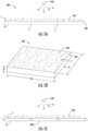
- Figures 1A through 1Care various illustrations of example wavelength conversion components 100, also referred to as a color conversion components and/or light converting element. In some embodiments, particularly when comprised of phosphor on sapphire, such components can be referred to herein as Phos hats.
- Figure 1Ais a side view illustration of a wavelength conversion components 100 comprising a clear substrate 102, or transparent substrate, and a phosphor compound 104 applied thereto.
- phospor compound 104can be applied to a top T or upper surface of clear substrate 102, as illustrated in Figure 1A .
- the phosphor compound 104is applied to a bottom B or lower surface of clear substrate 102.
- wavelength conversion components 100can comprise a substantially planar or wafer structure comprising a clear substrate 102 with a phosphor compound 104 applied to a surface thereof.
- Clear substrate 102can in some embodiments comprise a sapphire wafer, or other suitable clear or transparent material, such as for example glass of any kind, acrylic, soda lime, borosilicate, quartz/SiO 2 , MgF 2 .
- clear substrate 102can comprise a rigid or flexible clear substrate as well as a clear cure silicone sheet, which can provide the ability to shape a phosphor layer.
- Phosphor sheetscan comprise phosphor mixed into a silicone matrix and squeegeed flat and frozen to be used to lay onto a panel populated with die.
- Such a configurationcan provide a flexible Phos hat where the substrate can comprise for example a soft methyl.
- Such a configurationcan in some embodiments be vacuum attached and the soft silicone could conform and seal to a wet attach layer.
- the phosphor compound 104comprises phosphor and silicone.
- the phosphor compound 104can comprise a mixture of phosphor/silicone and another material, such as for example silicon (fumed silica), fused silica, TiO 2 , and other generic diffusers. Any scatterer, e.g. fused silica, can be added to the mixture for packing and homogeneity of emission. TiO 2 in small concentrations can in some embodiments be used effectively.
- the mixture of phosphor and siliconecomprises a ratio of about 1:1 to about 6:1, including about 1:1, about 2.5:1, about 3:1, about 4:1. about 4.5:1 and/or about 5:1.
- the concentration and/or particle size of the phosphor in the phosphor compoundis adjustable, wherein the concentration and/or particle size of the phosphor alters a color produced by a wavelength passing through the wavelength conversion component.
- Application A of the phosphor and/or phosphor compounds 104 to clear substrate 102can be achieved via any suitable method including, for example, spraying, gravity sedimentation, centrifuge, addition of a solvent, screen printing, evaporation (sputter, e-beam, thermal, CVD, electrostatic and/or electrophoretic deposition), dipping, spin coating, direct dispensing, and/or vibration, as discussed further herein.
- the phosphor compound 104is substantially uniformly applied to the transparent substrate 102 and/or is conformal to the transparent substrate 102.
- Wavelength conversion component 100 as shown in Figures 1A through 1Cis configured to alter a wavelength of a light emitted from a light source when positioned proximate to the light source, such as for example a LED.
- component 100is configured to be positioned on or proximate to a light source, such as an LED.
- wavelength conversion component 100can comprise any suitable size or configuration as needed for application to, on or near a light source such as an LED.
- width W , length L and height Hcan be configured as desired, e.g.
- a wavelength conversion component 100can be 40 um to 10 mm long and 5 um to 10 mm wide, or more, to achieve a wavelength conversion component 100 having an area of about 200 um 2 to about 5 mm 2 .
- a wavelength conversion component 100can be about 50 mm 2 or more.
- a wavelength conversion componentcan be any desirable size and/or shape, such as about 30 x 30 mm, which is an advantage not available in PiGs and CPPs.
- phosphor compound 104can be applied A to substrate 102 and then the wafer can be cut C into desired dimensions.
- substrate 102can in some embodiments be cut or singulated into clear substrates 102S prior to application A of phosphor compound 104.
- phosphor compound 104is applied to top surface T as well as along some edges or sides of clear substrate 102.
- wavelength conversion componentscan be made by providing a transparent substrate having an upper surface and a lower surface, applying a phosphor compound to the upper surface and/or lower surface of the transparent substrate, and curing the transparent substrate with applied phosphor compound.
- the resulting wavelength conversion componentcan in some embodiments be configured to alter a wavelength of a light emitted from a light source when positioned proximate to the light source.
- the transparent substratecan comprise a sapphire wafer.
- the phosphor compoundcomprises a mixture of phosphor and silicone.
- making the disclosed wavelength conversion components, or Phos hatscan further comprise using a stealth laser to cause an internal damage layer in the transparent substrate. Is some embodiments using the stealth laser to pitch can occur prior to application of the phosphor compound.
- phosphor and/or phosphor compounds to the clear or transparent substratecan be achieved via any suitable method including, for example, spraying, gravity sedimentation, centrifuge, addition of a solvent, screen printing, evaporation (sputter, e-beam, thermal, CVD, electrostatic and/or electrophoretic deposition), dipping, spin coating, direct dispensing, and/or vibration.
- the phosphor compoundcan be substantially uniformly applied to the transparent substrate such that it is conformal to the transparent substrate.
- a silicone compound and/or layercan be applied on the phosphor compound that is applied to the upper surface and/or lower surface of the transparent substrate.
- Figures 2A through 2Eare various illustrations of example LED devices as provided herein.
- Figures 2A through 2Ecan be viewed as steps for making/assembling a LED device as provided herein, although variations in the order of the steps and omission/addition of some steps is not precluded.
- Figure 2Adepicts a light emitter device 110 comprising a submount 112 and a plurality of light emitters 114a, 114b, and 114c disposed on submount 112. Any number of light emitters 114a-c, or LEDs, can be disposed on or applied to submount 112. Additionally, LEDs 114a-c can each have a different targeted color. Although three LEDs are illustrated, device 110 can include a different number of LEDs, e.g., a plurality of LEDs.
- a submount 112, or substratecan comprise electronic traces 116, or conductive traces, but in some examples, device 110 could be based on a leadframe construction where no traces are on top, or any other appropriate construction.
- die attach material 118, or solder bumpscan be provided to create an electrical contact between light emitters 114a-c and electronic traces 116.
- Figure 2Adepicts a light emitter device 110 comprising a submount 112 comprising an upper surface and a bottom surface and a plurality of light emitters 114a-c disposed on the upper surface of submount 112.
- the a plurality of light emitters 114a-ceach comprise an upper surface, a lower surface adjacent to the upper surface of submount 112, and one or more sides.
- a light affecting material 120can be applied to device 110.
- light affecting material 120can comprise a reflective material, such as for example TiO 2 (also referred to as titania and/or blue TiO 2 ), Al 2 O 3 , Boron nitride, microcellular polyethylene terephthalate (McPET) and/or Barium sulfate (sphere material).
- light affecting material 120is applied to device 110 so at to surround the plurality of light emitters 114a-c disposed on submount 112. That is, in some embodiments light affecting material 120 is disposed on the upper surface of submount 112 and adjacent to the one or more sides of the plurality of light emitters 114a-c.
- light affecting material 120is applied at a depth or height substantially similar to a height of light emitters 114a-c such that each side of light emitters 114a- c are surrounded by light affecting material 120 on one or more sides of light emitters 114a-c
- Light emitters 114a-ccan comprise any suitable chip size, shape, and/or thickness. In some aspects, the thickness or height can be approximately 0.25 mm or more, 0.3 mm or more, 0.4 mm or more, or 0.5 mm or more.
- Figure 2Cdepicts light emitter device 110 with a clear layer 122 applied to light emitters 114a-c.
- a clear layer 122in some embodiments comprising a silicone and/or an adhesive, and optionally a scatter compound, can be applied to an upper surface of the plurality of light emitters 114a-c.
- Clear or silicone layer 122can in some embodiments be configured to adhere the wavelength conversion component (see Figure 2D ) to the upper surface of the plurality of light emitters 114a-c.
- the scatter compoundcan comprise fumed silica, fused silica, and/or TiO 2 . In some aspects, TiO 2 in small percentages can be used for the scattering compound.
- the percentage of TiO 2can be from around, about or approximately 0.1% to 5.0%. In some aspects, the percentage of TiO 2 can for example be around, about or approximately 1%.
- Clear or silicone layer 122can be applied to the LEDs such that it substantially or completely covers the upper surface thereof. In some embodiments the clear layer can be administered such that it extends to the edges of the upper surface of the plurality of LEDs on the device, without extending past the edges.
- the wavelength conversion componentcan be applied to device 110 by placing the clear substrate 102 with phosphor layer 104 directly above light emitters 114a-c.
- the Phos hatcan affect the light output from the LEDs, including improving the uniformity of color produced by device 110.
- the Phos hatcan be applied with the phosphor 104 side down as depicted in Figure 2D .
- Clear layer 122can in some embodiments act as an adhesive to adhere substrate 102 with phosphor layer 104 onto light emitters 114a-c.
- a second application of light affecting material 124can be applied to device 110.
- light affecting material 124can comprise a reflective material, such as for example TiO 2 (also referred to as titania and/or blue TiO 2 ), and can be the same as light affecting material 120.
- Light affecting material 124is applied to device 110 so at to surround the Phos hat (substrate 102 and phosphor layer 104) on top of LEDs 114a-c.
- light affecting material 124is disposed on previously applied light affecting material 120 and adjacent to the one or more sides of the Phos hat (substrate 102 and phosphor layer 104) on top of LEDs 114a-c.
- this light affecting material 124is applied at a depth or height substantially similar to a height the Phos hat such that each side of it is surrounded by light affecting material 124.
- device 110can be cured at an appropriate temperature, such as for example 150°C.
- Figures 3A through 3Dvarious examples of LED devices as provided herein are illustrated.
- Figures 3A through 3Dcan be viewed as steps for making/assembling a LED device as provided herein, although variations in the order of the steps and omission/addition of some steps is not precluded.
- Figure 3Adepicts a light emitter device 110 comprising a submount 112 and the plurality of light emitters 114a, 114b, and 114c disposed on submount 112. Any number of light emitters 114a-c, or LEDs, can be disposed on or applied to submount 112. Additionally, LEDs 114a-c can each have a different targeted color. Although three LEDs are illustrated, device 110 can include a different number of LEDs, e.g., a plurality of LEDs.
- a submount 112, or substratecan comprise electronic traces 116, or conductive traces, but in some examples, device 110 could be based on a leadframe construction where no traces are on top, or any other appropriate construction.
- die attach material 118, or solder bumpscan be provided to create an electrical contact between light emitters 114a-c and electronic traces 116.
- Figure 3Adepicts a light emitter device 110 comprising a submount 112 comprising an upper surface and a bottom surface and a plurality of light emitters 114a-c disposed on the upper surface of submount 112.
- the plurality of light emitters 114a-ceach comprise an upper surface, a lower surface adjacent to the upper surface of submount 112, and one or more sides.
- Figure 3Bdepicts light emitter device 110 with a clear layer 122 applied to light emitters 114a-c.
- a clear layer 122in some embodiments comprising a silicone and/or an adhesive, and optionally a scatter compound, can be applied to an upper surface of the plurality of light emitters 114a-c.
- Clear or silicone layer 122can in some embodiments be configured to adhere the wavelength conversion component (see Figure 3C ) to the upper surface of the plurality of light emitters 114a-c.
- the scatter compoundcan comprise fumed and/or fused silica.
- Clear or silicone layer 122can be applied to the LEDs such that it substantially or completely covers the upper surface thereof.
- the clear layercan be administered such that it extends to the edges of the upper surface of the plurality of LEDs on the device, without extending past the edges.
- the wavelength conversion componentcan be applied to device 110 by placing the clear substrate 102 with phosphor layer 104 directly above light emitters 114a-c.
- the Phos hatcan affect the light output from the LEDs, including improving the uniformity of color produced by device 110.
- the Phos hatcan be applied with the phosphor 104 side down as depicted in Figure 3C .
- Clear layer 122can in some embodiments act as an adhesive to adhere substrate 102 with phosphor layer 104 onto light emitters 114a-c.
- a light affecting material 120can be applied to device 110.
- light affecting material 120can comprise a reflective material, such as for example TiO 2 .
- Light affecting material 120is applied to device 110 so at to surround the plurality of light emitters 114a-c disposed on submount 112, as well as the Phos hat (substrate 102 and phosphor layer 104) on top of LEDs 114a-c.
- light affecting material 120is disposed on the upper surface of submount 112 and adjacent to the one or more sides of the plurality of light emitters 114a-c.
- the light affecting material 120is applied at a depth or height substantially similar to a height of light emitters 114a-c, including the height of the Phos hat (substrate 102 and phosphor layer 104) on top of LEDs 114a-c, such that each side of light emitters 114a-c is surrounded by light affecting material 120.
- Figures 4A through 4Dvarious examples of LED devices as provided herein are illustrated.
- Figures 4A through 4Dcan be viewed as steps for making/assembling a LED device as provided herein, although variations in the order of the steps and omission/addition of some steps is not precluded.
- Figure 4Adepicts a light emitter device 110 comprising a submount 112 and a plurality of light emitters 114a, 114b, and 114c disposed on submount 112. Any number of light emitters 114a-c, or LEDs, can be disposed on or applied to submount 112. Additionally, LEDs 114a-c can each have a different targeted color. Although three LEDs are illustrated, device 110 can include a different number of LEDs, e.g., a plurality of LEDs.
- a submount 112, or substratecan comprise electronic traces 116, or conductive traces, but in some examples, device 110 could be based on a leadframe construction where no traces are on top, or any other appropriate construction.
- die attach material 118, or solder bumpscan be provided to create an electrical contact between light emitters 114a-c and electronic traces 116.
- Figure 4Adepicts a light emitter device 110 comprising a submount 112 comprising an upper surface and a bottom surface and a plurality of light emitters 114a-c disposed on the upper surface of submount 112.
- the plurality of light emitters 114a-ceach comprise an upper surface, a lower surface adjacent to the upper surface of submount 112, and one or more sides.
- Figure 4Bdepicts light emitter device 110 with a clear layer 122 applied to light emitters 114a-c.
- a clear layer 122in some embodiments comprising a silicone and/or an adhesive, and optionally a scatter compound, can be applied to an upper surface of the plurality of light emitters 114a-c.
- Clear or silicone layer 122can in some embodiments be configured to adhere the wavelength conversion component (see Figure 4C ) to the upper surface of the plurality of light emitters 114a-c.
- the scatter compoundcan comprise fumed and/or fused silica.
- Clear or silicone layer 122can be applied to the LEDs such that it substantially or completely covers the upper surface thereof.
- the clear layercan be administered such that it extends to the edges of the upper surface of the plurality of LEDs on the device, without extending past the edges.
- the wavelength conversion componentcan be applied to device 110 by placing the clear substrate 102 with phosphor layer 104 directly above light emitters 114a-c.
- the Phos hatcan affect the light output from the LEDs, including improving the uniformity of color produced by device 110.
- the Phos hatcan be applied with the phosphor 104 side down as depicted in Figure 4C .
- Clear layer 122can in some embodiments act as an adhesive to adhere substrate 102 with phosphor layer 104 onto light emitters 114a-c.
- a light affecting material 120can be applied to device 110.
- light affecting material 120can comprise a reflective material, such as for example TiO 2 .
- the light affecting material 120is applied to device 110 so at to surround the plurality of light emitters 114a-c disposed on submount 112, as well as the Phos hat (substrate 102 and phosphor layer 104) on top of LEDs 114a-c
- the light affecting material 120is disposed on the upper surface of submount 112 and adjacent to the one or more sides of the plurality of light emitters 114a-c.
- the light affecting material 120is applied at a depth or height substantially similar to a height of light emitters 114a-c, including the height of the Phos hat (substrate 102 and phosphor layer 104) on top of LEDs 114a-c, such that each side of light emitters 114a-c is surrounded by light affecting material 120.
- a dam material 130can be provided/applied by any suitable technique, e.g. molded, dispensed, etc., around a periphery of submount 112.
- Dam material 130can be configured to contain light affecting material 120 on the upper surface of submount 112 and/or adjacent to the one or more sides of the plurality of light emitters 114a-c whereby the plurality of light emitters is surrounded by the light affecting material.
- dam material 130can in some embodiments be configured to extend above the upper surface of submount 112 to a height substantially similar to a height of the one or more sides of the plurality of light emitters 114a-c, such that dam material 130 is configured to contain enough light affecting material 120 to surround the plurality of light emitters 114a-c at a depth substantially similar to the height of the one or more sides of the plurality of light emitters 114a-c.
- dam material 130can be more viscous than light affecting material 120.
- an upper surface of the light affecting material 120 encapsulating the plurality of light emitters 114a-cis substantially planar to the upper surface of the plurality of light emitters. That is, in the configuration depicted in Figure 4D the light affecting material 120 can be applied in such a manner as to create a squared off or substantially squared profile with an upper surface substantially planar to the upper surface of the LEDs/Phos hat, with an outer edge that is substantially vertical.
- dam material 130can be removed after application, and in some embodiments, curing of light affecting material 120.
- dam material 130can be configured as a high angle light reflector, such as for when light affecting material 120, or fill material, is clear. Dam material 130 can serve as a reflector of high angle light to make light more useful for application intent, especially when light affecting material 120 is a substantially transparent fill material.
- molded domescan be coupled with dam material 130 for light reflection to increase brightness, i.e. useful light. Such a configuration can be used with or without a wavelength conversion component or Phos hat as described herein.
- Dam material 130can in some embodiments comprise a mix of Si 5 with 50% TiO 2 , 50% 705F fused silica (roughly phosphor sized glass beads), and 5% A604 fumed silica. In some embodiments dam material 130 can comprise a mix of Si 4 , OE6370 silicone, 75% TiO 2 , 50% fused silica, and 7.5% fumed Silica.
- FIG 5is a perspective view of an example LED device 140, or LED chip, as disclosed herein.
- LED device 140can in some embodiments be the final product of the examples and steps depicted in Figures 2A-2E , 3A-3D and/or 4A-4D.
- LED device 140can in some embodiments comprise a submount 112 and a plurality of light emitters 114a, 114b, and 114c disposed on submount 112.
- Wavelength conversion component 100(or Phos hat comprising substrate 102 and phosphor layer 104 as depicted in Figures 2D , 3C and 4C ) is disposed on the upper surface of LEDs 114a-c.
- Light emitters 114a, 114b, and 114c and wavelength conversion component 100are surrounded by light affecting material 120.
- One or more contacts 128can be provided on substrate 112, and in some embodiments can extend under LEDs 114a-c and/or can be in electrical connection to electronic traces 116 (see Figures 2A , 3A and/or 4A) to provide electrical connections to LEDs 114a-c.
- Contacts 128can comprise one cathode and one anode.
- LED device 140can comprise a quick response code QR, or other bar code configured to contain information about the device.
- FIGS 6A and 6Bare top plan views of example LED devices 170 and 172, respectively.
- LED devices 170 and 172can in some embodiments comprise one light emitter 114 as depicted in Figure 6A , or a plurality of light emitters, such as for example two light emitters 114a/114b as depicted in Figure 6B , or more.
- a wavelength conversion component, or Phos hat, as disclosed hereinis disposed on the upper surface of the plurality of light emitters. Light emitters 114 or 114a/114b and the wavelength conversion component are surrounded by light affecting material 120.
- Figure 6Cdepicts a bottom plan view of an example LED device 170/172.
- the light emitterssuch as light emitters 114 in Figure 6A
- the light emitterscan be arranged for mounting using surface mount technology and having internal conductive paths, comprising first and second surface mount pads 176a and 176b, respectively, that can be formed on back surface 174 of submount 112.
- Conductive vias 178can be formed through submount 112 such that when a signal is applied to one or both of first and second surface mount pads 176a and 176b it is conducted to one or more electronic traces on the top surface of submount 112, such as electronic traces 116 depicted in Figures 2A , 3A and/or 4A.
- first and second mounting pads 176a and 176bcan allow for surface mounting of the LED devices 170/172 with the electrical signal to be applied to the LED devices 170/172 applied across the first and second mounting pads 176a and 176b.
- mounting pads 176a and 176b, and vias 178can be arranged in many different ways and can have many different shapes and sizes. It is also understood that instead of vias, one or more conductive traces can be provided on the surface of the submount between the mounting pads and contact pads, such as along the side surface of the submount.
- the LED device 170/172can further comprise a metallized area 180 on the back surface 174 of submount 112, between the first and second mounting pads 176a and 176b, respectively.
- Metallized area 180is preferably made of a heat conductive material and is preferably in at least partial vertical alignment the plurality of LEDs 114 ( Figure 6A ) or 114a , 114b ( Figure 6B ).
- the metallized area 180is not in electrical contact with the elements on top surface of the submount 112 or the first and second mounting pads 176a and 176b on the back surface 174 of the submount 112. Although heat from the LED is laterally spread over the top surface of the submount more heat will pass into the submount directly below and around the LED.
- the metallized areacan assist with this dissipation by allowing this heat to spread into the metallized area where it can dissipate more readily. It is also noted that the heat can conduct from the top surface of the submount 112, through the vias 178, where the heat can spread into the first and second mounting pads 176a and 176b where it can also dissipate.
- the thickness of the metallized area 180 and the first and second pads 176a and 176bshould be approximately the same such that all three make contact to a lateral surface such as a PCB.
- Figure 6Dis a side view of LED device 170/172, and illustrating an optiacal area, including light affecting material 120 near an upper surface, mounted on submount 112, with one or more copper traces 212 (or other conductive material such as Ni, Pd or Au) thereunder.
- FIG. 6Eis a top plan view of an example LED device 174.
- LED device 174can in some embodiments comprise a plurality of light emitters 114c and 114d, as depicted in Figure 6E .
- a wavelength conversion component, or Phos hat, as disclosed hereinis disposed on the upper surface of the plurality of light emitters.
- Light emitters 114c/114d and the wavelength conversion componentare surrounded by light affecting material 120.
- different phosphor regions, areas or zonescan be disposed over emitters 114c/114d.
- Emitters 114c/114dcan be any desired color, such as for example both emitters 114c/114d can comprise blue LEDs.
- the color emitted by the emitter or LEDcan be color shifted for example by the phosphor region or zone.
- US Patent No. 8,998,444discloses blue-shifted yellow and/or green plus (+) blue-shifted red.
- two or more zonescan be helpful where the emission spectrum of one phosphor overlaps with the activation (or excitation) spectrum of another phosphor.
- phosphors and phosphor colorscan be layered on each other and on a wavelength conversion component disposed over an emitter to produced different colors and/or color intensities.
- phosphorscan be optimally layered in one or more layers to achieve a light effect or desired wavelength. See, e.g., US Patent Application Publication No. 2009/0039375 .
- a first layercan comprise a red phosphor and a second layer a yellow phosphor, or vice versa.
- a green phosphorcan be layered on a yellow phosphor that is layered on a red phosphor, for example.
- emitterssuch as emitters 114c/114d in Figure 6E , with different phosphor colors thereon can be separately controllable such that they can be turned on at the same time or at different times.
- Figure 7is a plan view illustrating a metal trace configuration of an example LED device 150.
- the metalized trace depicted in Figure 6can comprise a metalized trace corresponding to LED device 140 of Figure 5 .
- LED device 150can comprise a substrate 126 (in some embodiments similar to substrate 112 of Figure 5 ) and one or more contacts 128, including one cathode and one anode.
- Connected to contacts 128can be one or more electronic traces 154 and/or contact pads 152, which can be configured to allow electric current to flow into and out of the solid state light emitters thereby illuminating the solid state light emitters.
- Solid state light emitterscan be electrically connected only in parallel, only in series, or in an arrangement comprising a combination of parallel and series.
- FIGS 8A and 8Bare various illustrations of example LED components 200 and 202, respectively.
- Each of components 200 and 202can in some embodiments comprise a substrate 210, such as an aluminum nitride substrate, and one or more copper traces 212 on substrate 210.
- a gold interface 216can be disposed on and/or above one or more copper traces 212.
- An aluminum pad 220 configured for wire bonding W an LEDcan be disposed on a portion of gold interface 216, with a layer of titanium 218 between aluminum pad 220 and gold interface 216.
- the layer of titanium 218can be configured to substantially prevent, or significantly reduce, galvanic action between aluminum pad 220 and gold interface 216.
- a light emitter 114can be disposed on gold interface 216.
- the layer of titanium 218 and aluminum pad 220can be substantially aligned vertically such that titanium 218 is substantially and directly below aluminum pad 220.
- aluminum pad 220can be disposed on top of a layer of titanium 218 that extends past the edges of aluminum pad 220.
- titanium 218is configured to extend beyond an outer periphery of aluminum pad 220 and provide an additional insulting effect against galvanic action between the aluminum pad and gold interface.
- FIG. 8Bshowing a top plan view of titanium 218 and aluminum pad 220, titanium 218 is configured to extend beyond an outer periphery of aluminum pad 220.
- a light emitter 114can for example be disposed on gold interface 216, and a wire W for wire bonding can for example extend from aluminum pad 220 for connecting to other structure.
- Such methodscan comprise providing an aluminum nitride substrate, providing one or more copper traces on the aluminum nitride substrate, providing a gold interface on the one or more copper traces, applying a first photo mask to create an opening on the gold interface and applying a layer of titanium thereon, and applying a second photo mask to create an opening on the layer of titanium and applying an aluminum pad configured for wire bonding the LED.
- Such a methodprovides an LED component as depicted in Figure 8B having a layer of titanium between the aluminum pad and gold interface, wherein the layer of titanium is configured to substantially prevent galvanic action between the aluminum pad and gold interface.
- Figure 9is an illustration of an example LED device 160.
- Figure 9depicts an LED device, such as that depicted in any of Figures 2A-2E , 3A-3D , 4A-4D and/or 5, enclosed in a lens 162.
- LED device 160can comprise a submount 112 and a plurality of light emitters 114 disposed on submount 112. Any number of light emitters 114 or LEDs can be disposed on or applied to submount 112.
- a submount 112, or substratecan comprise electronic traces 116, or conductive traces, but in some examples, device 110 could be based on a leadframe construction where no traces are on top, or any other appropriate construction.
- die attach material 118can be provided to create an electrical contact between light emitters 114 and electronic traces 116.
- a clear layer 122such as silicone, can be applied to light emitters 114 on top of which a wavelength conversion component (Phos hat), comprising clear substrate 102 with phosphor layer 104 directly, can be applied.
- a light affecting material 120can be applied to device 110 so at to surround the plurality of light emitters 114.
- a lens 162can be adhered to or otherwise affixed to substrate 112 and enclose light emitter 114, wavelength conversion component 102/104, and light affecting material 120. Lens 162 can provide a protective element to the LED and related components, and/or alter light emitted therefrom.
- LEDs used in the devices and components hereincan have different targeted colors selected so that devices can operate as a pixel and produce a range of colors within its color gamut by energizing different combinations of LEDs.
- LEDscan include UV, blue or green LED chips, such as a group III nitride based LED chip comprising negatively doped (n-type) epitaxial layer(s) of gallium nitride or its alloys and positively doped (p-type) epitaxial layers of gallium nitride or its alloys surrounding a light emitting active region; a red LED chip, such as an AlInGaP based red LED chip; a white LED chip (e.g., blue LED chip with phosphor(s) layer(s)), and/or a non-white phosphor based LED chip.
- group III nitride based LED chipcomprising negatively doped (n-type) epitaxial layer(s) of gallium nitride or its alloys and positively doped (p-type
- Traces, electrical contacts, leads and contact pads, as described herein,can comprise any suitable electrically conductive material, e.g., Cu, finished with electroless Ag, Ni-Ag, ENIG, ENIPIG, HASL, OSP, or the like. Traces can be applied over one or more surfaces of a substrate via plating (e.g., via electroplating or electroless plating), depositing (e.g., physical, chemical, and/or plasma deposition, CVD, PECVD, etc.), sputtering, or via any other suitable technique.
- platinge.g., via electroplating or electroless plating
- depositinge.g., physical, chemical, and/or plasma deposition, CVD, PECVD, etc.
- sputteringe.g., physical, chemical, and/or plasma deposition, CVD, PECVD, etc.
- tracescan comprise a metal or metal alloy which may contain (in whole or part) copper (Cu), silver (Ag), gold (Au), titanium (Ti), palladium (Pd), aluminum (Al), tin (Sn), combinations thereof, and/or any other suitable conductor.
- substratessuch as substrate 112 of Figures 2-5 , can comprise a printed circuit board (PCB), a metal core printed circuit board (MCPCB), a flexible printed circuit board, a dielectric laminate (e.g., FR-4 boards as known in the art), a ceramic based substrate, or any other suitable substrate for mounting LED chips and/or LED packages.
- PCBprinted circuit board
- MCPCBmetal core printed circuit board
- dielectric laminatee.g., FR-4 boards as known in the art
- ceramic based substratee.g., ceramic based substrate
- such substratescan comprise one or more materials arranged to provide desired electrical isolation and high thermal conductivity.
- at least a portion of such substratesmay comprise a dielectric to provide the desired electrical isolation between electrical traces and/or sets of solid state emitters.
- such substratescan comprise ceramic such as alumina (Al 2 O 3 ), aluminum nitride (AIN), silicon carbide (SiC), silicon, or a plastic or polymeric material such as polyimide, polyester etc.
- such substratescomprises a flexible circuit board, which can allow the substrate to take a non-planar or curved shape allowing for providing directional light emission with the solid state emitters also being arranged in a non-planar manner.
- LEDs 102a-ccan be horizontally structured so that LEDs 102a-c can be electrically connected to traces 108a-b without the use of wire bonding.
- each of LEDs 102a-ccan be a horizontally structured device where each electrical contact (e.g., the anode and cathode) can be disposed on a bottom surface of the LED 102a-c.
- Apparatus 100includes die attach material 130, e.g., solder bumps.
- Die attaching LEDs 102a-c using any suitable material and/or techniquecan directly electrically connect LEDs 102a-c to traces 108a-b without requiring wire bonds.
- each of LEDs 114a-ccan be a device that does not comprise angled or beveled surfaces.
- each of LEDs 114a-ccan be an LED device that comprises coplanar electrical contacts on one side of the LED (bottom side) with the majority of the light emitting or transmitting surface being located on the opposite side (upper side), also know as a "flip-chip”.
- LEDs 114a-ccan be bump bonded to traces using bumps of solder (or other appropriate conductive material) and force, energy (e.g., ultrasonic), and/or heat.
- LED devices 110, 140 and 160can optionally include diffuse layers for optics, lenses, polarizers, anti-reflective (AR) coating, anti glare, micro lenses, light steering, parallax barrier, lenticular arrays, and so on.
- diffuse layersfor optics, lenses, polarizers, anti-reflective (AR) coating, anti glare, micro lenses, light steering, parallax barrier, lenticular arrays, and so on.
- ARanti-reflective
- a method for making a wavelength conversion componentcomprises: providing a transparent substrate having an upper surface and a lower surface; applying a phosphor compound to the upper surface and/or lower surface of the transparent substrate; and curing the transparent substrate with applied phosphor compound, wherein the wavelength conversion component is configured to alter a wavelength of a light emitted from a light source when positioned proximate to the light source.
- the transparent substratecan comprise a sapphire wafer.
- the phosphor compoundcomprises a mixture of phosphor and silicone. The mixture of phosphor and silicone can comprise a ratio of about 1:1 to about 5:1.
- Applying a phosphor compound to the upper surface and/or lower surface of the transparent substrateresults in a substantially uniformly applied phosphor compound to the transparent substrate such that the phosphor compound is conformal to the transparent substrate.
- a lasercan be used to cause an internal damage layer in the transparent substrate.
- the methodcan comprise singulating the transparent substrate after application of the phosphor compound to provide a wavelength conversion component of a desired size, and the singulation can comprise singulating the transparent substrate prior to application of the phosphor compound to provide a wavelength conversion component of a desired size.
- Applying a phosphor compound to the upper surface and/or lower surface of the transparent substratecan comprise spraying, screen printing and/or dispensing.
- a silicone compound on the phosphor compoundcan be applied to the upper surface and/or lower surface of the transparent substrate.
- a method in some aspectscan comprise: providing a submount comprising an upper surface and a bottom surface; attaching the plurality of light emitters on the upper surface of the submount, the plurality of light emitters comprising an upper surface, a lower surface, and one or more sides; applying a light affecting material to the upper surface of the submount and adjacent to the one or more sides of the plurality of light emitters; and applying a wavelength conversion component on the upper surface of the plurality of light emitters.
- the light affecting materialcan comprise a reflective material.
- the light affecting materialcan comprise TiO 2 .
- the light affecting materialcan surround the sides of the plurality of light emitters disposed on the upper surface of the submount.
- Applying a light affecting materialcan further comprise applying a dam material on the upper surface of the submount prior to applying the light affecting material, wherein the dam material is configured to contain the light affecting material on the upper surface of the submount and adjacent to the one or more sides of the plurality of light emitters after application of the light affecting material, whereby the plurality of light emitters are surrounded by the light affecting material.
- the dam materialcan be applied on the upper surface of the submount to a height substantially similar to a height of the one or more sides of the plurality of light emitters, wherein the dam material is configured to contain enough light affecting material to surround the plurality of light emitters at a depth substantially similar to the height of the one or more sides of the plurality of light emitters.
- the wavelength conversion componentcan comprise a transparent substrate comprising an upper and lower surface, and a phosphor compound disposed on at least one or both of the upper and/or lower surface.
- the transparent substratecan comprise a sapphire wafer.
- the phosphor compoundcomprises a mixture of phosphor and silicone.
- the wavelength conversion componentcan be applied to the upper surface of the plurality of light emitters with the phosphor compound facing down and adjacent to the upper surface of the plurality of light emitters. Applying a wavelength conversion component on the upper surface of the plurality of light emitters further can comprise adding a silicone layer to the upper surface of the plurality of light emitters prior to applying the wavelength conversion component.
- the silicone layercan further comprise fumed or fused silica. Applying the light affecting material can occur prior to applying the wavelength conversion component.
- Applying the wavelength conversion componentcan occur prior to applying the light affecting material.
- a methodcan further comprise making the wavelength conversion component, comprising: providing a sapphire wafer having an upper surface and a lower surface; applying a phosphor compound to the upper surface and/or lower surface of the transparent substrate; and curing the transparent substrate with applied phosphor compound, wherein the wavelength conversion component is configured to alter a wavelength of a light emitted from a light source when positioned proximate to the light source.
- a light emitting diode (LED) componentcan comprise: a substrate for a light emitting diode (LED); one or more copper traces on the substrate; a gold interface on the one or more copper traces; an aluminum pad configured for electrically connecting with the LED; and a layer of titanium between the aluminum pad and gold interface, wherein the layer of titanium is configured to prevent, substantially prevent, or minimize galvanic action between the aluminum pad and gold interface.
- the layer of titaniumcan be configured to extend beyond an outer periphery of the aluminum pad.
- the substratecan be aluminum nitride.
- a method of making a light emitting diode (LED) componentcomprises: providing a substrate for a LED; providing one or more copper traces on the substrate; providing a gold interface on the one or more copper traces; applying a first photo mask to create an opening on the gold interface and applying a layer of titanium; and applying a second photo mask to create an opening on the layer of titanium and applying an aluminum pad configured for electrically connecting with the LED, wherein a layer of titanium is provided between the aluminum pad and gold interface, wherein the layer of titanium is configured to prevent, substantially prevent, or minimize galvanic action between the aluminum pad and gold interface.
- the layer of titaniumcan be configured to extend beyond an outer periphery of the aluminum pad.
- the substratecan be aluminum nitride.
- aspects disclosed hereincan, for example and without limitation, provide one or more of the following beneficial technical effects: reduced cost of providing solid state lighting apparatuses; reduced size, volume, or footprint of solid state lighting apparatuses; improved efficiency; improved color rendering; improved thermal management; simplified circuitry; improved contrast, improved viewing angle; improved color mixing; improved reliability; and/or simplified DC or AC operability.
Landscapes
- Engineering & Computer Science (AREA)
- Power Engineering (AREA)
- Microelectronics & Electronic Packaging (AREA)
- Physics & Mathematics (AREA)
- Condensed Matter Physics & Semiconductors (AREA)
- General Physics & Mathematics (AREA)
- Computer Hardware Design (AREA)
- Led Device Packages (AREA)
Description
- The subject matter disclosed herein relates generally to light emitting diodes (LEDs), components, and related methods. More particularly, the subject matter disclosed herein relates to devices, components and methods to improve emitting performance of LEDs.
- Light emitting diodes or LED chips are solid state devices that convert electrical energy into light. LED chips can be utilized in light emitter devices or components for providing different colors and patterns of light useful in various lighting and optoelectronic applications. Light emitter devices can include surface mount devices (SMDs) which can be mounted directly onto the surface of an underlying circuit component or heat sink, such as a printed circuit board (PCB) or metal core printed circuit board (MCPCB). SMDs can comprise bottom electrical contacts or leads configured to directly mount to the underlying circuit component. SMDs can be used in various LED light bulb and light fixture applications and are developing as replacements for incandescent, fluorescent, and metal halide high-intensity discharge (HID) lighting applications.
- Manufacturers of LED lighting products are constantly seeking ways to reduce their cost in order to provide a lower initial cost to customers, and encourage the adoption of LED products. Devices and components incorporating fewer raw materials at sustained or increased brightness levels are desired. Moreover, LEDs that produce light at optimal outputs and under enhance performance, particularly while using the same or less power, are becoming more desirable.
- Thus, despite the availability of various light emitter devices and components in the marketplace, a need remains for devices, components, and methods which can be produced quickly, efficiently, at a lower cost, and with improved performance characteristics.
US 2015/207045 ,EP 2216834 ,US 2011/049545 ,US 2011/018017 andUS 2016/079486 disclose a variety of light-emitting devices that include a phosphor layer known in the art.- In accordance with this disclosure, substrate based LEDs, components, and related methods having improved manufacturability and customization are provided and described herein. Devices, components, and methods described herein can advantageously exhibit improved processing times, ease of manufacture, and/or lower processing costs. Devices, components, and related methods described herein can be well suited for a variety of applications such as personal, industrial, and commercial lighting applications including, for example, light bulbs and light fixture products and/or applications. In some aspects, devices, components, and related methods described herein can comprise improved (e.g., less expensive and more efficient) manufacturing processes and/or improved optical properties including consistent color targeting and improved reflection.
- The present invention discloses a light emitter device according to claim 1 and a method for manufacturing a light emitter device according to
claim 10. Further embodiments are disclosed in the dependent claims. - A full and enabling disclosure of the present subject matter is set forth more particularly in the remainder of the specification, including reference to the accompanying figures, relating to one or more embodiments, in which:
Figures 1A through 1C are various illustrations of example wavelength conversion components;Figures 2A through 2E are various illustrations of example LED devices;Figures 3A through 3D are various illustrations of example LED devices;Figures 4A through 4D are various illustrations of example LED devices;Figure 5 is a perspective view of an example LED device;Figures 6A through 6E are various illustrations of example LED devices;Figure 7 is a plan view illustrating traces of an LED device;Figures 8A and 8B are various illustrations of example LED components; andFigure 9 is an illustration of an example LED device.- In some aspects, solid state lighting apparatuses and methods described herein can comprise various solid state light emitter electrical configurations, color combinations, and/or circuitry components for providing solid state lighting apparatuses having improved efficiency, improved color mixing, and/or improved color rendering. Apparatuses and methods such as those disclosed herein advantageously cost less, are more efficient, vivid, and/or brighter than some other solutions.
- Unless otherwise defined, terms used herein should be construed to have the same meaning as commonly understood by one of ordinary skill in the art to which this subject matter belongs. It will be further understood that terms used herein should be interpreted as having a meaning that is consistent with the respective meaning in the context of this specification and the relevant art, and should not be interpreted in an idealized or overly formal sense unless expressly so defined herein.
- Aspects of the subject matter are described herein with reference to sectional, perspective, elevation, and/or plan view illustrations that are schematic illustrations of idealized aspects of the subject matter. Variations from the shapes of the illustrations as a result, for example, of manufacturing techniques and/or tolerances, are to be expected, such that aspects of the subject matter should not be construed as limited to particular shapes illustrated herein. This subject matter can be embodied in different forms and should not be construed as limited to the specific aspects or embodiments set forth herein. In the drawings, the size and relative sizes of layers and regions can be exaggerated for clarity.
- Unless the absence of one or more elements is specifically recited, the terms "comprising," "including," and "having" as used herein should be interpreted as open-ended terms that do not preclude the presence of one or more elements. Like numbers refer to like elements throughout this description.
- It will be understood that when an element such as a layer, region, or substrate is referred to as being "on" another element, it can be directly on the other element or intervening elements can be present. Moreover, relative terms such as "on", "above", "upper", "top", "lower", or "bottom" are used herein to describe one structure's or portion's relationship to another structure or portion as illustrated in the figures. It will be understood that relative terms such as "on", "above", "upper", "top", "lower" or "bottom" are intended to encompass different orientations of the apparatus in addition to the orientation depicted in the figures. For example, if the apparatus in the figures is turned over, structure or portion described as "above" other structures or portions would now be oriented "below" the other structures or portions.
- The terms "electrically activated emitter(s)" and "emitter(s)" as used herein are synonymous terms and refer to any device capable of producing visible or near visible (e.g., from infrared to ultraviolet) wavelength radiation, including for example but not limited to, xenon lamps, mercury lamps, sodium lamps, incandescent lamps, and solid state emitters, including LEDs or LED chips, organic light emitting diodes (OLEDs), and lasers.
- The terms "solid state light emitter(s)", "solid state emitter(s)", and "light emitter(s)" are synonymous terms and refer to an LED chip, a laser diode, an organic LED chip, and/or any other semiconductor device preferably arranged as a semiconductor chip that comprises one or more semiconductor layers, which can comprise silicon, silicon carbide, gallium nitride and/or other semiconductor materials, a substrate which can comprise sapphire, silicon, silicon carbide and/or other microelectronic substrates, and one or more contact layers which can comprise metal and/or other conductive materials.
- The terms "groups", "segments", "strings", and "sets" as used herein are synonymous terms. As used herein, these terms generally describe how multiple LED chips are electrically connected, such as in series, in parallel, in mixed series/parallel, in common anode, or in common anode configurations among mutually exclusive groups/segments/sets. The segments of LED chips can be configured in a number of different ways and may have circuits of varying functionality associated therewith (e.g. driver circuits, rectifying circuits, current limiting circuits, shunts, bypass circuits, etc.), as discussed, for example, in commonly assigned and co-pending
U.S. Patent Application Serial No. 12/566,195, filed on September 24, 2009 U.S. Patent Application Serial No. 13/769,273, filed on February 15, 2013 U.S. Patent Application Serial No. 13/769,277 filed on February 15, 2013 U.S. Patent Application Serial No. 13/235,103, filed on September 16, 2011 U.S. Patent Application Serial No. 13/235,127, filed on September 16, 2011 U.S. Patent No. 8,729,589, which issued on May 20, 2014 . - The term "targeted" refers to configurations of LED chip segments that are configured to provide a pre-defined lighting characteristic that is a specified parameter for the lighting apparatus. For example, the targeted spectral power distribution can describe the characteristic of the light that is generated at a particular power, current, or voltage level.
- Apparatuses, systems, and methods as disclosed herein can utilize red chips, green chips, and blue chips. In some aspects, chips for use in blue-shifted yellow light (BSY) devices can target different bins as set forth in Table 1 of commonly owned, assigned, and co-pending
U.S. Patent Application Serial No. 12/257,804 , published asU.S. Pat. Pub. No. 2009/0160363 . Apparatuses, systems, and methods herein can utilize, for example, ultraviolet (UV) chips, cyan chips, blue chips, green chips, red chips, amber chips, and/or infrared chips. - The term "substrate" as used herein in connection with lighting apparatuses refers to a mounting member or element on which, in which, or over which, multiple solid state light emitters (e.g., LED chips) can be arranged, supported, and/or mounted. A substrate can be, e.g., a component substrate, a chip substrate (e.g., an LED substrate), or a sub-panel substrate. Exemplary substrates useful with lighting apparatuses as described herein can for example comprise printed circuit boards PCBs and/or related components (e.g., including but not limited to metal core printed circuit boards (MCPCBs), flexible circuit boards, dielectric laminates, ceramic based substrates, and the like, or ceramic boards having FR4 and/or electrical traces arranged on one or multiple surfaces thereof, high reflectivity ceramics (e.g., alumina) support panels, and/or mounting elements of various materials and conformations arranged to receive, support, and/or conduct electrical power to solid state emitters. Electrical traces described herein provide electrical power to the emitters for electrically activating and illuminating the emitters. Electrical traces may be visible and/or covered via a reflective covering, such as a solder mask material, Ag, or other suitable reflector.
- In some aspects, a single, unitary substrate can be used to support multiple groups of solid state light emitters in addition to at least some other circuits and/or circuit elements, such as a power or current driving components and/or current switching components. In other aspects, two or more substrates (e.g., at least a primary substrate and one or more secondary substrate or substrates) can be used to support multiple groups of solid state light emitters in addition to at least some other circuits and/or circuit elements, such as a power or current driving components and/or temperature compensation components. The first and second (e.g., primary and secondary) substrates can be disposed above and/or below each other and along different planes, adjacent (e.g., side-by-side) to each other, have one or more co-planar surfaces disposed adjacent each other, arranged vertically, arranged horizontally, and/or arranged in any other orientation with respect to each other.
- Solid state lighting apparatuses according to aspects of the subject matter herein can comprise III-V nitride (e.g., gallium nitride) based LED chips or laser chips fabricated on a silicon, silicon carbide, sapphire, or III-V nitride growth substrate, including (for example) chips manufactured and sold by Cree, Inc. of Durham, N.C. Such LED chips and/or lasers can be configured to operate such that light emission occurs through the substrate in a so-called "flip chip" orientation. Such LED and/or laser chips can also be devoid of growth substrates (e.g., following growth substrate removal). In some cases, LED chips can comprise red - III-V chips, but not nitride such as InGaAlP, GaAsP, and the like.
- LED chips useable with lighting apparatuses as disclosed herein can comprise horizontal structures (with both electrical contacts on a same side of the LED chip) and/or vertical structures (with electrical contacts on opposite sides of the LED chip). A horizontally structured chip (with or without the growth substrate), for example, can be flip chip bonded (e.g., using solder) to a carrier substrate or printed circuit board (PCB), or wire bonded. A vertically structured chip (without or without the growth substrate) can have a first terminal solder bonded to a carrier substrate, mounting pad, or printed circuit board (PCB), and have a second terminal wire bonded to the carrier substrate, electrical element, or PCB.
- Electrically activated light emitters, such as solid state emitters, can be used individually or in groups to emit light to stimulate emissions of one or more lumiphoric materials (e.g., phosphors, scintillators, lumiphoric inks, quantum dots), and generate light at one or more peak wavelengths, or of at least one desired perceived color (including combinations of colors that can be perceived as white). Inclusion of lumiphoric (also called 'luminescent') materials in lighting apparatuses as described herein can be accomplished by an application of a direct coating of the material on lumiphor support elements or lumiphor support surfaces (e.g., by powder coating, inkjet printing, or the like), adding such materials to lenses, and/or by embedding or dispersing such materials within lumiphor support elements or surfaces. Methods for fabricating LED chips having a planarized coating of phosphor integrated therewith are discussed by way of example in
U.S. Patent Application Publication No. 2008/0179611, filed on September 7, 2007, to Chitnis et al. . - Other materials, such as light scattering elements (e.g., particles) and/or index matching materials can be associated with a lumiphoric material-containing element or surface. Apparatuses and methods as disclosed herein can comprise LED chips of different colors, one or more of which can be white emitting (e.g., including at least one LED chip with one or more lumiphoric materials).
- In some aspects, a plurality of short wavelength solid state emitters (e.g., blue and/or cyan LED chips) can be used to stimulate emissions from a mixture of lumiphoric materials, or discrete layers of lumiphoric material, including red, yellow, and green lumiphoric materials. LED chips of different wavelengths can be present in the same group of solid state emitters, or can be provided in different groups of solid state emitters. A wide variety of wavelength conversion materials (e.g., luminescent materials, also known as lumiphors or lumiphoric media, e.g., as disclosed in
U.S. Pat. No. 6,600,175, issued on July 29, 2003 , andU.S. Patent Application Publication No. 2009/0184616, filed on October 9, 2008 . - In some aspects, lighting apparatuses and systems as described herein comprise multiple sets of solid state light emitters targeting different colors (e.g., one set targeting a first color and at least a second set targeting a second color that is different than the first color. In some aspects, each set of the multiple sets comprises at least two solid state light emitters of a same color (e.g., the peak wavelengths coincide). In some aspects, each set of the multiple sets of solid state emitters is adapted to emit one or more different color(s) of light. In some aspects, each set of the multiple sets of solid state emitters is adapted to emit one or more color(s) of light that differ relative to one another (e.g., with each set of solid state emitters emitting at least one peak wavelength that is not emitted by another set of solid state emitters). Aspects of targeting and selective activating sets of solid state emitters according to the present subject matter may be provided using the circuitry and/or techniques described in commonly assigned and co-pending
U.S. Patent Application Serial No. 14/221,839 . - The term "color" in reference to a solid state emitter refers to the color and/or wavelength of light that is emitted by the chip upon passage of electrical current therethrough.
- Some embodiments of the present subject matter may use solid state emitters, emitter packages, fixtures, luminescent materials/elements, power supply elements, control elements, and/or methods such as described in
U.S. Patent Nos. 7,564,180 ;7,456,499 ;7,213,940 ;7,095,056 ;6,958,497 ;6,853,010 ;6,791,119 ;6,600,175 ,6,201,262 ;6,187,606 ;6,120,600 ;5,912,477 ;5,739,554 ;5,631,190 ;5,604,135 ;5,523,589 ;5,416,342 ;5,393,993 ;5,359,345 ;5,338,944 ;5,210,051 ;5,027,168 ;5,027,168 ;4,966,862 , and/or4,918,497 , andU.S. Patent Application Publication Nos. 2009/0184616 ;2009/0080185 ;2009/0050908 ;2009/0050907 ;2008/0308825 ;2008/0198112 ;2008/0179611 ,2008/0173884 ,2008/0121921 ;2008/0012036 ;2007/0253209 ;2007/0223219 ;2007/0170447 ;2007/0158668 ;2007/0139923 , and/or 2006/0221272 ;U.S. Patent Application Serial No. 11/556,440, filed on December 4, 2006 - The terms "lighting apparatus" and "module" as used herein are synonymous, and are not limited, except that it is capable of emitting light. That is, a lighting apparatus can be a device or apparatus that illuminates an area or volume, e.g., a structure, a swimming pool or spa, a room, a warehouse, an indicator, a road, a parking lot, a vehicle, signage, e.g., road signs, a billboard, a ship, a toy, a mirror, a vessel, an electronic device, a boat, an aircraft, a stadium, a computer, a remote audio device, a remote video device, a cell phone, a tree, a window, an LCD display, a cave, a tunnel, a yard, a lamppost, or a device or array of devices that illuminate an enclosure, or a device that is used for edge or back-lighting (e.g., backlight poster, signage, LCD displays), light bulbs, bulb replacements (e.g., for replacing AC incandescent lights, low voltage lights, fluorescent lights, etc.), outdoor lighting, security lighting, exterior residential lighting (wall mounts, post/column mounts), ceiling fixtures/wall sconces, under cabinet lighting, lamps (floor and/or table and/or desk), landscape lighting, track lighting, task lighting, specialty lighting, rope lights, ceiling fan lighting, archival/art display lighting, high vibration/impact lighting-work lights, etc., mirrors/vanity lighting, spotlighting, high-bay lighting, low-bay lighting, or any other light emitting device.
- In some embodiments the LED devices provided herein can comprise a single wavelength conversion component, wavelength conversion materials, color conversion components and/or light converting elements. Such wavelength conversion components can comprise any suitable lumiphoric or phosphoric material, such as phosphors P, configured to emit a desired wavelength or light color, such as for example yellow, green, blue, red, and/or white, upon activation or impingement with light emitted by a plurality of LED chips of solid state light emitters. A wide variety of wavelength conversion materials or luminescent materials, also known as lumiphors or lumiphoric media, are disclosed in
U.S. Pat. No. 6,600,175, issued on July 29, 2003 , andU.S. Patent Application Publication No. 2009/0184616, filed on October 9, 2008 . - Phosphor and phosphor compounds as disclosed herein can comprise one or more of a wide variety of wavelength conversion materials or color conversion components including luminescent materials. Examples of luminescent materials (lumiphors) include phosphors, Cerium-doped Yttrium Aluminum Garnet (YAG), e.g. LuAG:Ce, Nitrides, Oxy-Nitrides, scintillators, day glow tapes, nanophosphors, quantum dots (e.g., such as provided by NNCrystal US Corp. (Fayetteville, Arkansas), and inks that glow in the visible spectrum upon illumination with (e.g., ultraviolet) light. Inclusion of lumiphors in wavelength conversion components, or related components as disclosed herein, in conjunction with solid state light emitters and LEDs can be accomplished by providing layers (e.g., coatings) of such materials over solid state emitters and/or by dispersing luminescent materials to a clear encapsulant (e.g., epoxy-based or silicone-based curable resin or other polymeric matrix) arranged to cover a plurality of solid state light emitters. One or more luminescent materials useable in devices as described herein may be down-converting or up-converting, or can include a combination of both types.
- Wavelength conversion materials, including those incorporated into the single wavelength conversion component as disclosed herein, can provide benefits including, for example, improved long term reliability (e.g., improved properties at around 1000 hours or more and 85°C, 105°C, and/or 125°C), decreased bubbling around solid state light emitters, a larger viewing angle, lower dCCT color spread, cooler phosphor temperatures, brighter light emission, improved sulfur resistance, and/or a smaller color point spread, including all or any combination of such features.
- As described herein, a plurality of LED chips can be at least partially covered with a wavelength conversion component comprising one or more phosphors and/or one or more layers of phosphors on a clear substrate, such as for example sapphire. In some embodiments the wavelength conversion component can be referred to as a phosphor-sapphire hat, or Phos hat. Phosphors can be adapted to emit blue light, yellow light, green light, red light, or any combination(s) thereof upon being impinged with light emitted via a plurality of LED chips. That is, in some aspects one or more phosphors in the Phos hat can absorb a portion of light emitted by the LED chip and in-turn reemit the absorbed light at a different wavelength such that the light emitter device or component emits a combination of light from each of the LED chip(s) and the phosphor(s). In one embodiment, the light emitter devices and components described herein can emit what is perceived as white light resulting from a combination of light emission from the LED chip and the Phos hat. In one embodiment according to the present subject matter, white emitting devices and components can consist of an LED chip that emits light in the blue wavelength spectrum and a phosphor in the Phos hat that absorbs some of the blue light and re-emits light in the green, yellow, and/or red wavelength spectrum. The devices and components can therefore emit a white light combination across the visible spectrum of light. In other embodiments, the LED chips with a wavelength conversion component, e.g. a Phos hat, can emit a non-white light combination of blue and yellow light as described in
U.S. Patent No. 7,213,940 . LED chips emitting red light or LED chips covered by a phosphor of a Phos hat that absorbs LED light and emits a red light is also contemplated herein. - The wavelength conversion component or Phos hat used in some embodiments with the disclosed LED components and devices can be made or assembled in any suitable manner. In some embodiments, the wavelength conversion component are produced by applying phosphor only on one surface of the Phos hat so that in assembly of an LED device or component the light affecting material (i.e., heavy scatterer to turn light) is right against or substantially adjacent to the Sapphire or Phos hat substrate, giving a clean edge for meniscus control.
- In the embodiments according to the present invention, the single wavelength conversion component is produced by spraying a substrate, e.g. LED chip, singulated on tape or other release material in a slightly spaced manner, which allows the phosphor to be applied on the sidewall of the substrate to form the Phos hat. This approach can in some aspects be useful where white-TiO2 light affecting material is not used or is applied prior to placing of the Phos hat, which can in some embodiments avoid blue light escaping from sides of a Phos hat.
- In some embodiments, substrate wafers can be sprayed, either above room temperature, i.e. hot, or at room temperature, to make the Phos hats. In some aspects it is suitable to spray the wafer at room temperature, followed by curing and then singulating of the die on the wafer.
- Other benefits of wavelength conversion materials (e.g., phosphor, P) used in the wavelength conversion component as disclosed herein, include, for example, improved far field images (e.g., thereby promoting a very uniform color appearance in the far field with a larger viewing angle), lower color shifts (lower dCCT), improved long term reliability (e.g., improved brightness maintenance (optics) at approximately 1000 hours or more), higher product ratings, cooler phosphor operating temperatures, and/or a lower color point spread, including all or any combination of such features.
- Phosphors are one known class of luminescent materials. A phosphor may refer to any material that absorbs light at one wavelength and re-emits light at a different wavelength in the visible spectrum, regardless of the delay between absorption and re-emission and regardless of the wavelengths involved. Accordingly, the term "phosphor" may be used herein to refer to materials that are sometimes called fluorescent and/or phosphorescent. In general, phosphors may absorb light having first wavelengths and re-emit light having second wavelengths that are different from the first wavelengths.
- The phosphor can emit radiation in the visible spectrum having lower energy than the radiation emitted by a light emitter and does so in response to the wavelength emitted by the emitter. Combinations of phosphors can be used in conjunction with the blue or UV-emitting chip/LED to create white light; e.g. blue and yellow, blue and green and red, and blue and green and yellow and red. Using three or more colors can provide an opportunity to select a particular white point and a better color rendering. It is also expected that LEDs with more than one emission peak will be useful in exciting one or more phosphors to produce white light.
- Phosphors and/or phosphor compounds can be selectively added and/or applied in any desired amount or quantity to clear or substantially clear substrates, wafers or sheets of material. Application of the phosphor and/or phosphor compounds can be achieved via any suitable method including, for example, spraying, gravity sedimentation, centrifugation, addition of a solvent, screen printing, evaporation (sputter, e-beam, thermal, CVD, electrostatic and/or electrophoretic deposition), dipping, spin coating, direct dispensing, and/or vibration, including for example as described in
U.S. Patent No. 8,410,679 to Ibbetson et al. , andU.S. Patent No. 8,425,271 to Hussell et al. . In some embodiments the phosphor compound applied to a clear substrate, e.g. sapphire wafer, is conformal to the shape and/or surface of the clear substrate. That is, a conformal layer of phosphor or phosphor compound can, for example, have an at least substantially uniform thickness. - The thickness of phosphor compound and/or phosphor layer on the clear substrate can, for example, range between approximately 2 µm and approximately 100 µm, however, any thickness of phosphor compound on the wavelength conversion component can be provided as desired. The thickness that is used may be selected to reduce or minimize blue light conversion in a planar surface, self-absorption and/or scattering, and may depend on the coating process, the density of the phosphor, other components in the phosphor compound, e.g. silicone, and/or the desired application.
- The disclosed wavelength conversion component, for example the Phos hat, can provide advantages over existing color changing elements used with solid state LEDs. For example, in some embodiments the presently disclosed subject matter, and particularly the Phos hats solve or significantly improve the problem of blue light conversion in a planar surface. In some embodiments, coupling the blueTiO2 processing, as discussed herein, with Phos hats can achieve top emitting performance from a bottom emitter die. These advantages are particularly evident as compared to the disadvantages of phosphor in glass (PiGs) and ceramic phosphor plate (CPP), which are widely used but are expensive to make.
- More particularly, PiGs are phosphor particles mixed with glass frit, pressed into wafer shapes, fired/sintered in high temperature ovens to become PiG-wafers that are then cut to size. CPP is a single crystal YAG phosphor boule that is grown and that is then watered and sawn into desired size. As disclosed herein, Phos hats utilize much simpler more readily available technology to achieve similar or improved results.
- As disclosed herein, Phos hats can comprise a sapphire wafer which is sprayed with a phosphor/silicone mixture to coat phosphor of the desired colorpoint onto a sapphire wafer/hat. Such Phos hats can in some embodiments have significant advantages, including for example cost, quick turn, very low capital, and sharper corners and flatter surfaces than sintered PiGs. Moreover, there are fewer or no voids or mixing problems as is common with PiGs. Furthermore, there is substantially reduced or no contamination as is common with PiGs. Additionally, PiGs have shrinkage during sintering causing uneven thicknesses and thus uneven color conversion. Also, PiGs are subject to extreme brittleness so therefore are limited to minimum thicknesses for handling. Conversely, Phos hats can be relatively thin (<80um) as sapphire wafers are very durable.
- As for CPPs, they are inherently expensive to make, such as for example an order of magnitude more expensive.
- Another advantage over existing technology is Phos hats are tunable or adjustable. For example, when spraying, or other appropriate application technique as discussed herein, phosphor compounds on a pre-singulated sapphire wafer, this allows the ability to check color within minutes. Post initial spray a Phos hat can be plucked off, tested, and if needed the remaining PhoS wafer can be quick-sprayed to add more phosphor or phosphor compound as needed to tune in the color point.
- The disclosed wavelength conversion component, or Phos hat, can comprise a glass or other suitable substrate, i.e. a clear or substantially clear substrate, for light extraction such as sapphire, acrylic, etc. Phos hats can be made on large substrates, including large sapphire wafers, for example, with larger surface areas as compared to exiting options. Moreover, they can be made uniformly across the wide area, thus they can be matched to die wavelengths to achieve tight color control on product. Conversely, PiGs and CPPs are made in much smaller wafer sizes. Because in some embodiments a spray application is used, scattering particles and different phosphors can be mixed together to achieve an array of diffusion and color/CRI points. CPP cannot do this. Moreover, PiGs may not be able to do this as the temperatures required may breakdown some components that would work with Phos hats.
- In some embodiments all flip chip die can benefit from the disclosed wavelength conversion component by turning a 3D phosphor emission plane into a 2D emission plane. Additionally, an advantage is that EZ die can be made into "WZ-like" die with this lower cost method.
- Robustness of LED devices can also be greatly enhanced with the disclosed components given their hard top or solid upper surface versus a silicone top, which is flexible, in traditional LED devices. Such hard-top or robust LED devices can be useful in applications requiring such strength, including for example automotive applications. Moreover, sulfur resistance can in some embodiments be greatly enhanced over silicone encapsulated components.
- Various illustrative features are described below in connection with the accompanying figures.
Figures 1A through 1C are various illustrations of examplewavelength conversion components 100, also referred to as a color conversion components and/or light converting element. In some embodiments, particularly when comprised of phosphor on sapphire, such components can be referred to herein as Phos hats.Figure 1A is a side view illustration of awavelength conversion components 100 comprising aclear substrate 102, or transparent substrate, and aphosphor compound 104 applied thereto. In some examples,phospor compound 104 can be applied to a topT or upper surface ofclear substrate 102, as illustrated inFigure 1A . Within the scope of the present claims, thephosphor compound 104 is applied to a bottomB or lower surface ofclear substrate 102. In some embodiments, thephosphor compound 104 may be applied on both topT and bottomB. As illustrated inFigure 1B ,wavelength conversion components 100 can comprise a substantially planar or wafer structure comprising aclear substrate 102 with aphosphor compound 104 applied to a surface thereof.Clear substrate 102 can in some embodiments comprise a sapphire wafer, or other suitable clear or transparent material, such as for example glass of any kind, acrylic, soda lime, borosilicate, quartz/SiO2, MgF2. In some embodimentsclear substrate 102 can comprise a rigid or flexible clear substrate as well as a clear cure silicone sheet, which can provide the ability to shape a phosphor layer. Phosphor sheets can comprise phosphor mixed into a silicone matrix and squeegeed flat and frozen to be used to lay onto a panel populated with die. Such a configuration can provide a flexible Phos hat where the substrate can comprise for example a soft methyl. Such a configuration can in some embodiments be vacuum attached and the soft silicone could conform and seal to a wet attach layer.- The
phosphor compound 104 comprises phosphor and silicone. In some embodiments thephosphor compound 104 can comprise a mixture of phosphor/silicone and another material, such as for example silicon (fumed silica), fused silica, TiO2, and other generic diffusers. Any scatterer, e.g. fused silica, can be added to the mixture for packing and homogeneity of emission. TiO2 in small concentrations can in some embodiments be used effectively. In some embodiments the mixture of phosphor and silicone comprises a ratio of about 1:1 to about 6:1, including about 1:1, about 2.5:1, about 3:1, about 4:1. about 4.5:1 and/or about 5:1. In some aspects the concentration and/or particle size of the phosphor in the phosphor compound is adjustable, wherein the concentration and/or particle size of the phosphor alters a color produced by a wavelength passing through the wavelength conversion component. - ApplicationA of the phosphor and/or
phosphor compounds 104 toclear substrate 102 can be achieved via any suitable method including, for example, spraying, gravity sedimentation, centrifuge, addition of a solvent, screen printing, evaporation (sputter, e-beam, thermal, CVD, electrostatic and/or electrophoretic deposition), dipping, spin coating, direct dispensing, and/or vibration, as discussed further herein. In some aspects, thephosphor compound 104 is substantially uniformly applied to thetransparent substrate 102 and/or is conformal to thetransparent substrate 102. Wavelength conversion component 100 as shown inFigures 1A through 1C is configured to alter a wavelength of a light emitted from a light source when positioned proximate to the light source, such as for example a LED. Thus, as discussed further herein,component 100 is configured to be positioned on or proximate to a light source, such as an LED. In some embodiments, and as shown inFigure 1B ,wavelength conversion component 100 can comprise any suitable size or configuration as needed for application to, on or near a light source such as an LED. For example, widthW , lengthL and heightH can be configured as desired, e.g. 40 um to 10 mm long and 5 um to 10 mm wide, or more, to achieve awavelength conversion component 100 having an area of about 200 um2 to about 5 mm2. In some embodiments awavelength conversion component 100 can be about 50 mm2 or more. By way of example and not limitation, a wavelength conversion component can be any desirable size and/or shape, such as about 30 x 30 mm, which is an advantage not available in PiGs and CPPs.- As illustrated in
Figure 1A , in someembodiments phosphor compound 104 can be appliedA tosubstrate 102 and then the wafer can be cutC into desired dimensions. Alternatively, as illustrated inFigure 1C ,substrate 102 can in some embodiments be cut or singulated into clear substrates102S prior to applicationA ofphosphor compound 104. In the approach depicted inFigure 1C phosphor compound 104 is applied to top surfaceT as well as along some edges or sides ofclear substrate 102. - In some embodiments wavelength conversion components, or Phos hats, can be made by providing a transparent substrate having an upper surface and a lower surface, applying a phosphor compound to the upper surface and/or lower surface of the transparent substrate, and curing the transparent substrate with applied phosphor compound. The resulting wavelength conversion component can in some embodiments be configured to alter a wavelength of a light emitted from a light source when positioned proximate to the light source. The transparent substrate can comprise a sapphire wafer. The phosphor compound comprises a mixture of phosphor and silicone.
- In some embodiments making the disclosed wavelength conversion components, or Phos hats, can further comprise using a stealth laser to cause an internal damage layer in the transparent substrate. Is some embodiments using the stealth laser to pitch can occur prior to application of the phosphor compound.
- Application of the phosphor and/or phosphor compounds to the clear or transparent substrate can be achieved via any suitable method including, for example, spraying, gravity sedimentation, centrifuge, addition of a solvent, screen printing, evaporation (sputter, e-beam, thermal, CVD, electrostatic and/or electrophoretic deposition), dipping, spin coating, direct dispensing, and/or vibration. The phosphor compound can be substantially uniformly applied to the transparent substrate such that it is conformal to the transparent substrate.
- In some embodiments, a silicone compound and/or layer can be applied on the phosphor compound that is applied to the upper surface and/or lower surface of the transparent substrate.
Figures 2A through 2E are various illustrations of example LED devices as provided herein. In some embodimentsFigures 2A through 2E can be viewed as steps for making/assembling a LED device as provided herein, although variations in the order of the steps and omission/addition of some steps is not precluded.Figure 2A depicts alight emitter device 110 comprising asubmount 112 and a plurality oflight emitters submount 112. Any number oflight emitters 114a-c, or LEDs, can be disposed on or applied tosubmount 112. Additionally,LEDs 114a-c can each have a different targeted color. Although three LEDs are illustrated,device 110 can include a different number of LEDs, e.g., a plurality of LEDs.- In some embodiments a
submount 112, or substrate, can compriseelectronic traces 116, or conductive traces, but in some examples,device 110 could be based on a leadframe construction where no traces are on top, or any other appropriate construction. In some embodiments die attachmaterial 118, or solder bumps, can be provided to create an electrical contact betweenlight emitters 114a-c andelectronic traces 116. - In some embodiments
Figure 2A depicts alight emitter device 110 comprising asubmount 112 comprising an upper surface and a bottom surface and a plurality oflight emitters 114a-c disposed on the upper surface ofsubmount 112. In some embodiments the a plurality oflight emitters 114a-c each comprise an upper surface, a lower surface adjacent to the upper surface ofsubmount 112, and one or more sides. - Turning to
Figure 2B , alight affecting material 120 can be applied todevice 110. In some embodiments light affectingmaterial 120 can comprise a reflective material, such as for example TiO2 (also referred to as titania and/or blue TiO2), Al2O3, Boron nitride, microcellular polyethylene terephthalate (McPET) and/or Barium sulfate (sphere material). In some embodiments light affectingmaterial 120 is applied todevice 110 so at to surround the plurality oflight emitters 114a-c disposed onsubmount 112. That is, in some embodiments light affectingmaterial 120 is disposed on the upper surface ofsubmount 112 and adjacent to the one or more sides of the plurality oflight emitters 114a-c. In some embodiments light affectingmaterial 120 is applied at a depth or height substantially similar to a height oflight emitters 114a-c such that each side oflight emitters 114a-c are surrounded bylight affecting material 120 on one or more sides oflight emitters 114a-c Light emitters 114a-c can comprise any suitable chip size, shape, and/or thickness. In some aspects, the thickness or height can be approximately 0.25 mm or more, 0.3 mm or more, 0.4 mm or more, or 0.5 mm or more. By applying the reflective or light affecting material on the sides of the LEDs light emitted from the sides of the LEDs can minimized thereby focusing the light emission from an upper surface of the LEDs. In some embodiments light affectingmaterial 120 surroundslight emitters 114a-c and fills any voids or filets there between, as depicted inFigure 2B . Figure 2C depictslight emitter device 110 with aclear layer 122 applied tolight emitters 114a-c. Particularly, in some embodiments aclear layer 122, in some embodiments comprising a silicone and/or an adhesive, and optionally a scatter compound, can be applied to an upper surface of the plurality oflight emitters 114a-c. Clear orsilicone layer 122 can in some embodiments be configured to adhere the wavelength conversion component (seeFigure 2D ) to the upper surface of the plurality oflight emitters 114a-c. The scatter compound can comprise fumed silica, fused silica, and/or TiO2. In some aspects, TiO2 in small percentages can be used for the scattering compound. For example, the percentage of TiO2 can be from around, about or approximately 0.1% to 5.0%. In some aspects, the percentage of TiO2 can for example be around, about or approximately 1%. Clear orsilicone layer 122 can be applied to the LEDs such that it substantially or completely covers the upper surface thereof. In some embodiments the clear layer can be administered such that it extends to the edges of the upper surface of the plurality of LEDs on the device, without extending past the edges.- As depicted in
Figure 2D , the wavelength conversion component, or Phos hat, can be applied todevice 110 by placing theclear substrate 102 withphosphor layer 104 directly abovelight emitters 114a-c. By disposing wavelength conversion component on the upper surface of the plurality of light emitters the Phos hat can affect the light output from the LEDs, including improving the uniformity of color produced bydevice 110. In some embodiments, the Phos hat can be applied with thephosphor 104 side down as depicted inFigure 2D .Clear layer 122 can in some embodiments act as an adhesive to adheresubstrate 102 withphosphor layer 104 ontolight emitters 114a-c. - In
Figure 2E a second application oflight affecting material 124 can be applied todevice 110. In some embodiments light affectingmaterial 124 can comprise a reflective material, such as for example TiO2 (also referred to as titania and/or blue TiO2), and can be the same aslight affecting material 120.Light affecting material 124 is applied todevice 110 so at to surround the Phos hat (substrate 102 and phosphor layer104) on top ofLEDs 114a-c. In this embodimentlight affecting material 124 is disposed on previously appliedlight affecting material 120 and adjacent to the one or more sides of the Phos hat (substrate 102 and phosphor layer104) on top ofLEDs 114a-c. In thislight affecting material 124 is applied at a depth or height substantially similar to a height the Phos hat such that each side of it is surrounded bylight affecting material 124. By applying the reflective or light affecting material on the sides of the Phos hat light emitted from the sides of the LEDs and the Phos hat on top thereof can be minimized thereby focusing the light emission from an upper surface of the LEDs and Phos hat. - In some
embodiments device 110, including that depicted inFigure 2E , can be cured at an appropriate temperature, such as for example 150°C. - Turning now to
Figures 3A through 3D , various examples of LED devices as provided herein are illustrated. In some embodimentsFigures 3A through 3D can be viewed as steps for making/assembling a LED device as provided herein, although variations in the order of the steps and omission/addition of some steps is not precluded.Figure 3A depicts alight emitter device 110 comprising asubmount 112 and the plurality oflight emitters submount 112. Any number oflight emitters 114a-c, or LEDs, can be disposed on or applied tosubmount 112. Additionally,LEDs 114a-c can each have a different targeted color. Although three LEDs are illustrated,device 110 can include a different number of LEDs, e.g., a plurality of LEDs. - In some embodiments a
submount 112, or substrate, can compriseelectronic traces 116, or conductive traces, but in some examples,device 110 could be based on a leadframe construction where no traces are on top, or any other appropriate construction. In some embodiments die attachmaterial 118, or solder bumps, can be provided to create an electrical contact betweenlight emitters 114a-c andelectronic traces 116. - In some embodiments
Figure 3A depicts alight emitter device 110 comprising asubmount 112 comprising an upper surface and a bottom surface and a plurality oflight emitters 114a-c disposed on the upper surface ofsubmount 112. In some embodiments the plurality oflight emitters 114a-c each comprise an upper surface, a lower surface adjacent to the upper surface ofsubmount 112, and one or more sides. Figure 3B depictslight emitter device 110 with aclear layer 122 applied tolight emitters 114a-c. Particularly, in some embodiments aclear layer 122, in some embodiments comprising a silicone and/or an adhesive, and optionally a scatter compound, can be applied to an upper surface of the plurality oflight emitters 114a-c. Clear orsilicone layer 122 can in some embodiments be configured to adhere the wavelength conversion component (seeFigure 3C ) to the upper surface of the plurality oflight emitters 114a-c. The scatter compound can comprise fumed and/or fused silica. Clear orsilicone layer 122 can be applied to the LEDs such that it substantially or completely covers the upper surface thereof. In some embodiments the clear layer can be administered such that it extends to the edges of the upper surface of the plurality of LEDs on the device, without extending past the edges.- As depicted in
Figure 3C , the wavelength conversion component, or Phos hat, can be applied todevice 110 by placing theclear substrate 102 withphosphor layer 104 directly abovelight emitters 114a-c. By disposing wavelength conversion component on the upper surface of the plurality of light emitters the Phos hat can affect the light output from the LEDs, including improving the uniformity of color produced bydevice 110. In some embodiments, the Phos hat can be applied with thephosphor 104 side down as depicted inFigure 3C .Clear layer 122 can in some embodiments act as an adhesive to adheresubstrate 102 withphosphor layer 104 ontolight emitters 114a-c. - Turning to
Figure 3D , alight affecting material 120 can be applied todevice 110. In some embodiments light affectingmaterial 120 can comprise a reflective material, such as for example TiO2.Light affecting material 120 is applied todevice 110 so at to surround the plurality oflight emitters 114a-c disposed onsubmount 112, as well as the Phos hat (substrate 102 and phosphor layer104) on top ofLEDs 114a-c. In this embodimentlight affecting material 120 is disposed on the upper surface ofsubmount 112 and adjacent to the one or more sides of the plurality oflight emitters 114a-c. Thelight affecting material 120 is applied at a depth or height substantially similar to a height oflight emitters 114a-c, including the height of the Phos hat (substrate 102 and phosphor layer104) on top ofLEDs 114a-c, such that each side oflight emitters 114a-c is surrounded bylight affecting material 120. By applying the reflective or light affecting material on the sides of the LEDs light emitted from the sides of the LEDs can minimized thereby focusing the light emission from an upper surface of the LEDs and Phos hat. - Turning now to
Figures 4A through 4D , various examples of LED devices as provided herein are illustrated. In some embodimentsFigures 4A through 4D can be viewed as steps for making/assembling a LED device as provided herein, although variations in the order of the steps and omission/addition of some steps is not precluded.Figure 4A depicts alight emitter device 110 comprising asubmount 112 and a plurality oflight emitters submount 112. Any number oflight emitters 114a-c, or LEDs, can be disposed on or applied tosubmount 112. Additionally,LEDs 114a-c can each have a different targeted color. Although three LEDs are illustrated,device 110 can include a different number of LEDs, e.g., a plurality of LEDs. - In some embodiments a
submount 112, or substrate, can compriseelectronic traces 116, or conductive traces, but in some examples,device 110 could be based on a leadframe construction where no traces are on top, or any other appropriate construction. In some embodiments die attachmaterial 118, or solder bumps, can be provided to create an electrical contact betweenlight emitters 114a-c andelectronic traces 116. - In some embodiments
Figure 4A depicts alight emitter device 110 comprising asubmount 112 comprising an upper surface and a bottom surface and a plurality oflight emitters 114a-c disposed on the upper surface ofsubmount 112. In some embodiments the plurality oflight emitters 114a-c each comprise an upper surface, a lower surface adjacent to the upper surface ofsubmount 112, and one or more sides. Figure 4B depictslight emitter device 110 with aclear layer 122 applied tolight emitters 114a-c. Particularly, in some embodiments aclear layer 122, in some embodiments comprising a silicone and/or an adhesive, and optionally a scatter compound, can be applied to an upper surface of the plurality oflight emitters 114a-c. Clear orsilicone layer 122 can in some embodiments be configured to adhere the wavelength conversion component (seeFigure 4C ) to the upper surface of the plurality oflight emitters 114a-c. The scatter compound can comprise fumed and/or fused silica. Clear orsilicone layer 122 can be applied to the LEDs such that it substantially or completely covers the upper surface thereof. In some embodiments the clear layer can be administered such that it extends to the edges of the upper surface of the plurality of LEDs on the device, without extending past the edges.- As depicted in
Figure 4C , the wavelength conversion component, or Phos hat, can be applied todevice 110 by placing theclear substrate 102 withphosphor layer 104 directly abovelight emitters 114a-c. By disposing wavelength conversion component on the upper surface of the plurality of light emitters the Phos hat can affect the light output from the LEDs, including improving the uniformity of color produced bydevice 110. In some embodiments, the Phos hat can be applied with thephosphor 104 side down as depicted inFigure 4C .Clear layer 122 can in some embodiments act as an adhesive to adheresubstrate 102 withphosphor layer 104 ontolight emitters 114a-c. - Turning to
Figure 4D , alight affecting material 120 can be applied todevice 110. In some embodiments light affectingmaterial 120 can comprise a reflective material, such as for example TiO2. In this embodiment thelight affecting material 120 is applied todevice 110 so at to surround the plurality oflight emitters 114a-c disposed onsubmount 112, as well as the Phos hat (substrate 102 and phosphor layer104) on top ofLEDs 114a-cThelight affecting material 120 is disposed on the upper surface ofsubmount 112 and adjacent to the one or more sides of the plurality oflight emitters 114a-c. Thelight affecting material 120 is applied at a depth or height substantially similar to a height oflight emitters 114a-c, including the height of the Phos hat (substrate 102 and phosphor layer104) on top ofLEDs 114a-c, such that each side oflight emitters 114a-c is surrounded bylight affecting material 120. In order to containlight affecting material 120 on the upper surface of the submount and adjacent to the one or more sides of the plurality of light emitters adam material 130 can be provided/applied by any suitable technique, e.g. molded, dispensed, etc., around a periphery ofsubmount 112.Dam material 130 can be configured to containlight affecting material 120 on the upper surface ofsubmount 112 and/or adjacent to the one or more sides of the plurality oflight emitters 114a-c whereby the plurality of light emitters is surrounded by the light affecting material. In some embodiments, and as depicted inFigure 4D ,dam material 130 can in some embodiments be configured to extend above the upper surface ofsubmount 112 to a height substantially similar to a height of the one or more sides of the plurality oflight emitters 114a-c, such thatdam material 130 is configured to contain enoughlight affecting material 120 to surround the plurality oflight emitters 114a-c at a depth substantially similar to the height of the one or more sides of the plurality oflight emitters 114a-c. In someembodiments dam material 130 can be more viscous than light affectingmaterial 120. In some embodiments, an upper surface of thelight affecting material 120 encapsulating the plurality oflight emitters 114a-c is substantially planar to the upper surface of the plurality of light emitters. That is, in the configuration depicted inFigure 4D thelight affecting material 120 can be applied in such a manner as to create a squared off or substantially squared profile with an upper surface substantially planar to the upper surface of the LEDs/Phos hat, with an outer edge that is substantially vertical. In someembodiments dam material 130 can be removed after application, and in some embodiments, curing oflight affecting material 120. By applying the reflective or light affecting material on the sides of the LEDs light emitted from the sides of the LEDs can minimized thereby focusing the light emission from an upper surface of the LEDs and Phos hat. Such effect can be further enhanced and/or optimized in some embodiments by providing the light affecting/reflective material in a squared-off configuration as depicted inFigure 4D . - In some
embodiments dam material 130 can be configured as a high angle light reflector, such as for when light affectingmaterial 120, or fill material, is clear.Dam material 130 can serve as a reflector of high angle light to make light more useful for application intent, especially when light affectingmaterial 120 is a substantially transparent fill material. In some embodiments molded domes can be coupled withdam material 130 for light reflection to increase brightness, i.e. useful light. Such a configuration can be used with or without a wavelength conversion component or Phos hat as described herein. Dam material 130 can in some embodiments comprise a mix of Si5 with 50% TiO2, 50% 705F fused silica (roughly phosphor sized glass beads), and 5% A604 fumed silica. In someembodiments dam material 130 can comprise a mix of Si4, OE6370 silicone, 75% TiO2, 50% fused silica, and 7.5% fumed Silica.Figure 5 is a perspective view of anexample LED device 140, or LED chip, as disclosed herein.LED device 140 can in some embodiments be the final product of the examples and steps depicted inFigures 2A-2E ,3A-3D and/or 4A-4D.LED device 140 can in some embodiments comprise asubmount 112 and a plurality oflight emitters submount 112. Wavelength conversion component100 (or Phoshat comprising substrate 102 andphosphor layer 104 as depicted inFigures 2D ,3C and4C ) is disposed on the upper surface ofLEDs 114a-c.Light emitters wavelength conversion component 100 are surrounded bylight affecting material 120. One ormore contacts 128 can be provided onsubstrate 112, and in some embodiments can extend underLEDs 114a-c and/or can be in electrical connection to electronic traces116 (seeFigures 2A ,3A and/or 4A) to provide electrical connections toLEDs 114a-c.Contacts 128 can comprise one cathode and one anode. In some embodiments,LED device 140 can comprise a quick response codeQR, or other bar code configured to contain information about the device.Figures 6A and 6B are top plan views ofexample LED devices LED devices light emitter 114 as depicted inFigure 6A , or a plurality of light emitters, such as for example twolight emitters 114a/114b as depicted inFigure 6B , or more. A wavelength conversion component, or Phos hat, as disclosed herein is disposed on the upper surface of the plurality of light emitters.Light emitters light affecting material 120.Figure 6C depicts a bottom plan view of anexample LED device 170/172. In some embodiments the light emitters, such aslight emitters 114 inFigure 6A , can be arranged for mounting using surface mount technology and having internal conductive paths, comprising first and secondsurface mount pads 176a and176b, respectively, that can be formed onback surface 174 ofsubmount 112.Conductive vias 178 can be formed throughsubmount 112 such that when a signal is applied to one or both of first and secondsurface mount pads 176a and176b it is conducted to one or more electronic traces on the top surface ofsubmount 112, such aselectronic traces 116 depicted inFigures 2A ,3A and/or 4A. In some embodiments, first andsecond mounting pads 176a and176b can allow for surface mounting of theLED devices 170/172 with the electrical signal to be applied to theLED devices 170/172 applied across the first andsecond mounting pads 176a and176b.- It is understood that the mounting
pads 176a and176b, and vias178 can be arranged in many different ways and can have many different shapes and sizes. It is also understood that instead of vias, one or more conductive traces can be provided on the surface of the submount between the mounting pads and contact pads, such as along the side surface of the submount. - The
LED device 170/172 can further comprise a metallizedarea 180 on theback surface 174 ofsubmount 112, between the first andsecond mounting pads 176a and176b, respectively.Metallized area 180 is preferably made of a heat conductive material and is preferably in at least partial vertical alignment the plurality of LEDs114 (Figure 6A ) or114a,114b (Figure 6B ). In one embodiment, the metallizedarea 180 is not in electrical contact with the elements on top surface of thesubmount 112 or the first andsecond mounting pads 176a and176b on theback surface 174 of thesubmount 112. Although heat from the LED is laterally spread over the top surface of the submount more heat will pass into the submount directly below and around the LED. The metallized area can assist with this dissipation by allowing this heat to spread into the metallized area where it can dissipate more readily. It is also noted that the heat can conduct from the top surface of thesubmount 112, through thevias 178, where the heat can spread into the first andsecond mounting pads 176a and176b where it can also dissipate. For theLED device 170/172 used in surface mounting, the thickness of the metallizedarea 180 and the first andsecond pads 176a and176b should be approximately the same such that all three make contact to a lateral surface such as a PCB. Figure 6D is a side view ofLED device 170/172, and illustrating an optiacal area, includinglight affecting material 120 near an upper surface, mounted onsubmount 112, with one or more copper traces212 (or other conductive material such as Ni, Pd or Au) thereunder.Figure 6E is a top plan view of anexample LED device 174.LED device 174 can in some embodiments comprise a plurality oflight emitters Figure 6E . A wavelength conversion component, or Phos hat, as disclosed herein is disposed on the upper surface of the plurality of light emitters.Light emitters 114c/114d and the wavelength conversion component are surrounded bylight affecting material 120. As shown inFigure 6E , in some embodiments different phosphor regions, areas or zones can be disposed overemitters 114c/114d. Any combinations of phosphors and colors are possible, including for example a red phosphor region or zone overemitter 114c, and a separate yellow and/or green phosphor region or zone overemitter 114d.Emitters 114c/114d, can be any desired color, such as for example bothemitters 114c/114d can comprise blue LEDs. The color emitted by the emitter or LED can be color shifted for example by the phosphor region or zone.US Patent No. 8,998,444 , discloses blue-shifted yellow and/or green plus (+) blue-shifted red.- In some embodiments two or more zones can be helpful where the emission spectrum of one phosphor overlaps with the activation (or excitation) spectrum of another phosphor. In some embodiments, phosphors and phosphor colors can be layered on each other and on a wavelength conversion component disposed over an emitter to produced different colors and/or color intensities. For example, phosphors can be optimally layered in one or more layers to achieve a light effect or desired wavelength. See, e.g.,
US Patent Application Publication No. 2009/0039375 . For example, a first layer can comprise a red phosphor and a second layer a yellow phosphor, or vice versa. Additionally, a green phosphor can be layered on a yellow phosphor that is layered on a red phosphor, for example. Moreover, emitters, such asemitters 114c/114d inFigure 6E , with different phosphor colors thereon can be separately controllable such that they can be turned on at the same time or at different times. Figure 7 is a plan view illustrating a metal trace configuration of anexample LED device 150. In some embodiments the metalized trace depicted inFigure 6 can comprise a metalized trace corresponding toLED device 140 ofFigure 5 .LED device 150 can comprise a substrate126 (in some embodiments similar tosubstrate 112 ofFigure 5 ) and one ormore contacts 128, including one cathode and one anode. Connected tocontacts 128 can be one or moreelectronic traces 154 and/orcontact pads 152, which can be configured to allow electric current to flow into and out of the solid state light emitters thereby illuminating the solid state light emitters. Solid state light emitters can be electrically connected only in parallel, only in series, or in an arrangement comprising a combination of parallel and series.Figures 8A and 8B are various illustrations ofexample LED components components substrate 210, such as an aluminum nitride substrate, and one or more copper traces212 onsubstrate 210. Agold interface 216 can be disposed on and/or above one or more copper traces212. Analuminum pad 220 configured for wire bondingW an LED can be disposed on a portion ofgold interface 216, with a layer oftitanium 218 betweenaluminum pad 220 andgold interface 216. The layer oftitanium 218 can be configured to substantially prevent, or significantly reduce, galvanic action betweenaluminum pad 220 andgold interface 216. Alight emitter 114 can be disposed ongold interface 216.- In
Figure 8A the layer oftitanium 218 andaluminum pad 220 can be substantially aligned vertically such thattitanium 218 is substantially and directly belowaluminum pad 220. Alternatively, inFigure 8B aluminum pad 220 can be disposed on top of a layer oftitanium 218 that extends past the edges ofaluminum pad 220. As such,titanium 218 is configured to extend beyond an outer periphery ofaluminum pad 220 and provide an additional insulting effect against galvanic action between the aluminum pad and gold interface. As depicted in the inset ofFigure 8B , showing a top plan view oftitanium 218 andaluminum pad 220,titanium 218 is configured to extend beyond an outer periphery ofaluminum pad 220. Alight emitter 114 can for example be disposed ongold interface 216, and a wireW for wire bonding can for example extend fromaluminum pad 220 for connecting to other structure. - In some embodiments provided herein are methods of making a LED component such as those depicted in
Figures 8A and 8B . Such methods can comprise providing an aluminum nitride substrate, providing one or more copper traces on the aluminum nitride substrate, providing a gold interface on the one or more copper traces, applying a first photo mask to create an opening on the gold interface and applying a layer of titanium thereon, and applying a second photo mask to create an opening on the layer of titanium and applying an aluminum pad configured for wire bonding the LED. Such a method provides an LED component as depicted inFigure 8B having a layer of titanium between the aluminum pad and gold interface, wherein the layer of titanium is configured to substantially prevent galvanic action between the aluminum pad and gold interface. Figure 9 is an illustration of anexample LED device 160.Figure 9 depicts an LED device, such as that depicted in any ofFigures 2A-2E ,3A-3D ,4A-4D and/or 5, enclosed in alens 162.LED device 160 can comprise asubmount 112 and a plurality oflight emitters 114 disposed onsubmount 112. Any number oflight emitters 114 or LEDs can be disposed on or applied tosubmount 112. In some embodiments asubmount 112, or substrate, can compriseelectronic traces 116, or conductive traces, but in some examples,device 110 could be based on a leadframe construction where no traces are on top, or any other appropriate construction. In some embodiments die attachmaterial 118, or solder bumps, can be provided to create an electrical contact betweenlight emitters 114 andelectronic traces 116. In some embodiments aclear layer 122, such as silicone, can be applied tolight emitters 114 on top of which a wavelength conversion component (Phos hat), comprisingclear substrate 102 withphosphor layer 104 directly, can be applied. Finally, as discussed herein, alight affecting material 120 can be applied todevice 110 so at to surround the plurality oflight emitters 114. Alens 162 can be adhered to or otherwise affixed tosubstrate 112 and encloselight emitter 114,wavelength conversion component 102/104, andlight affecting material 120.Lens 162 can provide a protective element to the LED and related components, and/or alter light emitted therefrom.- In some examples, LEDs used in the devices and components herein can have different targeted colors selected so that devices can operate as a pixel and produce a range of colors within its color gamut by energizing different combinations of LEDs. For example, LEDs can include UV, blue or green LED chips, such as a group III nitride based LED chip comprising negatively doped (n-type) epitaxial layer(s) of gallium nitride or its alloys and positively doped (p-type) epitaxial layers of gallium nitride or its alloys surrounding a light emitting active region; a red LED chip, such as an AlInGaP based red LED chip; a white LED chip (e.g., blue LED chip with phosphor(s) layer(s)), and/or a non-white phosphor based LED chip.
- Traces, electrical contacts, leads and contact pads, as described herein, can comprise any suitable electrically conductive material, e.g., Cu, finished with electroless Ag, Ni-Ag, ENIG, ENIPIG, HASL, OSP, or the like. Traces can be applied over one or more surfaces of a substrate via plating (e.g., via electroplating or electroless plating), depositing (e.g., physical, chemical, and/or plasma deposition, CVD, PECVD, etc.), sputtering, or via any other suitable technique. In some aspects, traces can comprise a metal or metal alloy which may contain (in whole or part) copper (Cu), silver (Ag), gold (Au), titanium (Ti), palladium (Pd), aluminum (Al), tin (Sn), combinations thereof, and/or any other suitable conductor.
- In some aspects, substrates, such as
substrate 112 ofFigures 2-5 , can comprise a printed circuit board (PCB), a metal core printed circuit board (MCPCB), a flexible printed circuit board, a dielectric laminate (e.g., FR-4 boards as known in the art), a ceramic based substrate, or any other suitable substrate for mounting LED chips and/or LED packages. In some aspects such substrates can comprise one or more materials arranged to provide desired electrical isolation and high thermal conductivity. For example, at least a portion of such substrates may comprise a dielectric to provide the desired electrical isolation between electrical traces and/or sets of solid state emitters. In some aspects, such substrates can comprise ceramic such as alumina (Al2O3), aluminum nitride (AIN), silicon carbide (SiC), silicon, or a plastic or polymeric material such as polyimide, polyester etc. In some aspects, such substrates comprises a flexible circuit board, which can allow the substrate to take a non-planar or curved shape allowing for providing directional light emission with the solid state emitters also being arranged in a non-planar manner. - In some aspects, LEDs 102a-c can be horizontally structured so that LEDs 102a-c can be electrically connected to traces 108a-b without the use of wire bonding. For example, each of LEDs 102a-c can be a horizontally structured device where each electrical contact (e.g., the anode and cathode) can be disposed on a bottom surface of the LED 102a-c.
Apparatus 100 includes die attachmaterial 130, e.g., solder bumps. Die attaching LEDs 102a-c using any suitable material and/or technique (e.g., solder attachment, preform attachment, flux or no-flux eutectic attachment, silicone epoxy attachment, metal epoxy attachment, thermal compression attachment, bump bonding, and/or combinations thereof) can directly electrically connect LEDs 102a-c to traces 108a-b without requiring wire bonds. - In some aspects, each of
LEDs 114a-c can be a device that does not comprise angled or beveled surfaces. For example, each ofLEDs 114a-c can be an LED device that comprises coplanar electrical contacts on one side of the LED (bottom side) with the majority of the light emitting or transmitting surface being located on the opposite side (upper side), also know as a "flip-chip".LEDs 114a-c can be bump bonded to traces using bumps of solder (or other appropriate conductive material) and force, energy (e.g., ultrasonic), and/or heat. - In some aspects,
LED devices - In some aspects, a method for making a wavelength conversion component, comprises: providing a transparent substrate having an upper surface and a lower surface; applying a phosphor compound to the upper surface and/or lower surface of the transparent substrate; and curing the transparent substrate with applied phosphor compound, wherein the wavelength conversion component is configured to alter a wavelength of a light emitted from a light source when positioned proximate to the light source. The transparent substrate can comprise a sapphire wafer. The phosphor compound comprises a mixture of phosphor and silicone. The mixture of phosphor and silicone can comprise a ratio of about 1:1 to about 5:1. Applying a phosphor compound to the upper surface and/or lower surface of the transparent substrate results in a substantially uniformly applied phosphor compound to the transparent substrate such that the phosphor compound is conformal to the transparent substrate. A laser can be used to cause an internal damage layer in the transparent substrate. The method can comprise singulating the transparent substrate after application of the phosphor compound to provide a wavelength conversion component of a desired size, and the singulation can comprise singulating the transparent substrate prior to application of the phosphor compound to provide a wavelength conversion component of a desired size. Applying a phosphor compound to the upper surface and/or lower surface of the transparent substrate can comprise spraying, screen printing and/or dispensing. A silicone compound on the phosphor compound can be applied to the upper surface and/or lower surface of the transparent substrate.
- A method in some aspects can comprise: providing a submount comprising an upper surface and a bottom surface; attaching the plurality of light emitters on the upper surface of the submount, the plurality of light emitters comprising an upper surface, a lower surface, and one or more sides; applying a light affecting material to the upper surface of the submount and adjacent to the one or more sides of the plurality of light emitters; and applying a wavelength conversion component on the upper surface of the plurality of light emitters. The light affecting material can comprise a reflective material. The light affecting material can comprise TiO2. The light affecting material can surround the sides of the plurality of light emitters disposed on the upper surface of the submount. Applying a light affecting material can further comprise applying a dam material on the upper surface of the submount prior to applying the light affecting material, wherein the dam material is configured to contain the light affecting material on the upper surface of the submount and adjacent to the one or more sides of the plurality of light emitters after application of the light affecting material, whereby the plurality of light emitters are surrounded by the light affecting material. The dam material can be applied on the upper surface of the submount to a height substantially similar to a height of the one or more sides of the plurality of light emitters, wherein the dam material is configured to contain enough light affecting material to surround the plurality of light emitters at a depth substantially similar to the height of the one or more sides of the plurality of light emitters. The wavelength conversion component can comprise a transparent substrate comprising an upper and lower surface, and a phosphor compound disposed on at least one or both of the upper and/or lower surface. The transparent substrate can comprise a sapphire wafer. The phosphor compound comprises a mixture of phosphor and silicone. The wavelength conversion component can be applied to the upper surface of the plurality of light emitters with the phosphor compound facing down and adjacent to the upper surface of the plurality of light emitters. Applying a wavelength conversion component on the upper surface of the plurality of light emitters further can comprise adding a silicone layer to the upper surface of the plurality of light emitters prior to applying the wavelength conversion component. The silicone layer can further comprise fumed or fused silica. Applying the light affecting material can occur prior to applying the wavelength conversion component. Applying the wavelength conversion component can occur prior to applying the light affecting material. A method can further comprise making the wavelength conversion component, comprising: providing a sapphire wafer having an upper surface and a lower surface; applying a phosphor compound to the upper surface and/or lower surface of the transparent substrate; and curing the transparent substrate with applied phosphor compound, wherein the wavelength conversion component is configured to alter a wavelength of a light emitted from a light source when positioned proximate to the light source.
- In some aspects, a light emitting diode (LED) component, can comprise: a substrate for a light emitting diode (LED); one or more copper traces on the substrate; a gold interface on the one or more copper traces; an aluminum pad configured for electrically connecting with the LED; and a layer of titanium between the aluminum pad and gold interface, wherein the layer of titanium is configured to prevent, substantially prevent, or minimize galvanic action between the aluminum pad and gold interface. The layer of titanium can be configured to extend beyond an outer periphery of the aluminum pad. The substrate can be aluminum nitride.
- In some aspects, a method of making a light emitting diode (LED) component comprises: providing a substrate for a LED; providing one or more copper traces on the substrate; providing a gold interface on the one or more copper traces; applying a first photo mask to create an opening on the gold interface and applying a layer of titanium; and applying a second photo mask to create an opening on the layer of titanium and applying an aluminum pad configured for electrically connecting with the LED, wherein a layer of titanium is provided between the aluminum pad and gold interface, wherein the layer of titanium is configured to prevent, substantially prevent, or minimize galvanic action between the aluminum pad and gold interface. The layer of titanium can be configured to extend beyond an outer periphery of the aluminum pad. The substrate can be aluminum nitride.
- While the subject matter has been has been described herein in reference to specific aspects, features, and illustrative embodiments, it will be appreciated that the utility of the subject matter is not thus limited, but rather extends to and encompasses numerous other variations, modifications and alternative embodiments, as will suggest themselves to those of ordinary skill in the field of the present subject matter, based on the disclosure herein.
- Aspects disclosed herein can, for example and without limitation, provide one or more of the following beneficial technical effects: reduced cost of providing solid state lighting apparatuses; reduced size, volume, or footprint of solid state lighting apparatuses; improved efficiency; improved color rendering; improved thermal management; simplified circuitry; improved contrast, improved viewing angle; improved color mixing; improved reliability; and/or simplified DC or AC operability.
- Various combinations and sub-combinations of the structures and features described herein are contemplated and will be apparent to a skilled person having knowledge of this disclosure. Any of the various features and elements as disclosed herein can be combined with one or more other disclosed features and elements unless indicated to the contrary herein.
- The scope of the invention is defined by the appended claims.
Claims (10)
- A light emitter device (110) comprising:a submount (112) comprising an upper surface and a bottom surface;plurality of light emitters (114a-c) disposed on the upper surface of the submount (112), the plurality of light emitters (114a-c) comprising an upper surface and one or more sides;a light affecting material (120, 124) disposed on the upper surface of the submount (112) and adjacent to the one or more sides of the plurality of light emitters (114a-c); anda single wavelength conversion component (100) disposed over the upper surface of the plurality of light emitters (114a-c), wherein the wavelength conversion component (100) comprises (i) a transparent substrate (102) comprising an upper substrate surface and a lower substrate surface, and (ii) a spray-coated phosphor material (104) disposed on the lower substrate surface,characterized in that the spray-coated phosphor material (104) comprises a mixture of phosphor and silicone, and wherein the spray-coated phosphor material (104) is further disposed on a sidewall of the transparent substrate (102).
- The light emitter device (110) of claim 1, wherein the transparent substrate (102) comprises sapphire.
- The light emitter device (110) of any one of claims 1 to 2, wherein the spray-coated phosphor material (104) is substantially uniformly applied to the transparent substrate and/or is conformal to the transparent substrate (102).
- The light emitter device (110) of claim 1, further comprising a clear layer (122) between the wavelength conversion component (100) and the upper surface of the plurality of light emitters (114a-c).
- The light emitter device (110) of claim 4, wherein the clear layer (122) comprises a silicone and/or an adhesive, and optionally comprises a scattering compound.
- The light emitter device (110) of claim 5, wherein the clear layer (122) comprises a scattering compound that comprises fumed silica, fused silica, and/or TiO2.
- The light emitter device (110) of any one of claims 1 to 6, wherein the light affecting material (120, 124) comprises a light-reflective material.
- The light emitter device (110) of any one of claims 1 to 7, further comprising one or more electrically conductive contacts (176a-b) disposed on the bottom surface of the submount (112).
- The light emitter device (110) of any one of claims 1 to 8, further comprising one or more electrical traces (154) on the submount (112), wherein at least one light emitter of the plurality of light emitters (114a-c) is electrically connected to the one or more electrical traces (154).
- A method for fabricating a light emitter device (110) that comprises a submount (112) and plurality of light emitters (114a-c) disposed on the upper surface of the submount (112), with the plurality of light emitters (114a-c) comprising an upper surface and one or more sides, the method comprising:providing a light affecting material (120, 124) on the upper surface of the submount (112) adjacent to the one or more sides of the plurality of light emitters (114a-c); andapplying a single wavelength conversion component (100) over the upper surface of the plurality of light emitters (114a-c), wherein the wavelength conversion component (100) comprises (i) a transparent substrate (102) comprising an upper substrate surface and a lower substrate surface, and (ii) a spray-coated phosphor material (104) disposed on the lower substrate surface, wherein the spray-coated phosphor material (104) comprises a mixture of phosphor and silicone, and wherein the spray-coated phosphor material (104) is further disposed on a sidewall of the transparent substrate (102)
Applications Claiming Priority (2)
| Application Number | Priority Date | Filing Date | Title |
|---|---|---|---|
| US201662366961P | 2016-07-26 | 2016-07-26 | |
| PCT/US2017/043316WO2018022456A1 (en) | 2016-07-26 | 2017-07-21 | Light emitting diodes, components and related methods |
Publications (2)
| Publication Number | Publication Date |
|---|---|
| EP3491679A1 EP3491679A1 (en) | 2019-06-05 |
| EP3491679B1true EP3491679B1 (en) | 2023-02-22 |
Family
ID=59523255
Family Applications (1)
| Application Number | Title | Priority Date | Filing Date |
|---|---|---|---|
| EP17748998.6AActiveEP3491679B1 (en) | 2016-07-26 | 2017-07-21 | Light emitting diodes, components and related methods |
Country Status (4)
| Country | Link |
|---|---|
| US (4) | US10290777B2 (en) |
| EP (1) | EP3491679B1 (en) |
| CN (1) | CN109791968A (en) |
| WO (1) | WO2018022456A1 (en) |
Families Citing this family (46)
| Publication number | Priority date | Publication date | Assignee | Title |
|---|---|---|---|---|
| EP3491679B1 (en) | 2016-07-26 | 2023-02-22 | CreeLED, Inc. | Light emitting diodes, components and related methods |
| JP6724634B2 (en)* | 2016-07-28 | 2020-07-15 | 日亜化学工業株式会社 | Method for manufacturing light emitting device |
| JP6769248B2 (en)* | 2016-11-09 | 2020-10-14 | 日亜化学工業株式会社 | Light emitting device |
| FR3069378B1 (en)* | 2017-07-21 | 2019-08-23 | Aledia | OPTOELECTRONIC DEVICE |
| US10242891B2 (en) | 2017-08-24 | 2019-03-26 | Cerebras Systems Inc. | Apparatus and method for securing components of an integrated circuit |
| JP6665872B2 (en) | 2018-01-15 | 2020-03-13 | 日亜化学工業株式会社 | Light emitting device and method of manufacturing light emitting device |
| CN110176529B (en)* | 2018-02-20 | 2022-03-08 | 晶元光电股份有限公司 | Light-emitting element and method of making the same |
| US20190267525A1 (en) | 2018-02-26 | 2019-08-29 | Semicon Light Co., Ltd. | Semiconductor Light Emitting Devices And Method Of Manufacturing The Same |
| EP3785307A1 (en) | 2018-04-23 | 2021-03-03 | Cree, Inc. | Semiconductor light emitting devices including superstrates with patterned surfaces |
| US11121298B2 (en) | 2018-05-25 | 2021-09-14 | Creeled, Inc. | Light-emitting diode packages with individually controllable light-emitting diode chips |
| DE102018119323A1 (en)* | 2018-08-08 | 2020-02-13 | Osram Opto Semiconductors Gmbh | Method for producing conversion elements, conversion elements, method for producing a light-emitting semiconductor component and light-emitting semiconductor component |
| TWI676851B (en)* | 2018-08-22 | 2019-11-11 | 隆達電子股份有限公司 | Pixel array package structure and display panel |
| US11233183B2 (en) | 2018-08-31 | 2022-01-25 | Creeled, Inc. | Light-emitting diodes, light-emitting diode arrays and related devices |
| USD902448S1 (en) | 2018-08-31 | 2020-11-17 | Cree, Inc. | Light emitting diode package |
| US11335833B2 (en) | 2018-08-31 | 2022-05-17 | Creeled, Inc. | Light-emitting diodes, light-emitting diode arrays and related devices |
| CN111009603A (en)* | 2018-10-04 | 2020-04-14 | 日亚化学工业株式会社 | light-emitting device |
| JP6959548B2 (en)* | 2018-10-04 | 2021-11-02 | 日亜化学工業株式会社 | Light emitting device and its manufacturing method |
| US10971401B2 (en) | 2018-10-16 | 2021-04-06 | Cerebras Systems Inc. | Systems and methods for precision fabrication of an orifice within an integrated circuit |
| JP7157327B2 (en)* | 2018-10-30 | 2022-10-20 | 日亜化学工業株式会社 | light emitting device |
| JP6940776B2 (en)* | 2018-11-05 | 2021-09-29 | 日亜化学工業株式会社 | Light emitting device and its manufacturing method |
| TWI686651B (en)* | 2018-11-23 | 2020-03-01 | 友達光電股份有限公司 | Backlight module |
| TWI695212B (en)* | 2018-11-23 | 2020-06-01 | 友達光電股份有限公司 | Backlight module |
| US11437551B2 (en) | 2019-03-19 | 2022-09-06 | Seoul Viosys Co., Ltd. | Light emitting device package and application thereof |
| KR102723703B1 (en)* | 2019-05-28 | 2024-10-31 | 삼성디스플레이 주식회사 | Display device and manufacturing method for display device |
| US11101411B2 (en) | 2019-06-26 | 2021-08-24 | Creeled, Inc. | Solid-state light emitting devices including light emitting diodes in package structures |
| JP6849139B1 (en)* | 2019-08-02 | 2021-03-24 | 日亜化学工業株式会社 | Light emitting device and surface emitting light source |
| JP7189446B2 (en)* | 2019-08-08 | 2022-12-14 | 日亜化学工業株式会社 | Light-emitting device and method for manufacturing light-emitting device |
| JP7339518B2 (en)* | 2019-09-18 | 2023-09-06 | 日亜化学工業株式会社 | Method for manufacturing light-emitting module |
| US11083059B2 (en) | 2019-10-03 | 2021-08-03 | Creeled, Inc. | Lumiphoric arrangements for light emitting diode packages |
| US11145530B2 (en)* | 2019-11-08 | 2021-10-12 | Cerebras Systems Inc. | System and method for alignment of an integrated circuit |
| US11837684B2 (en) | 2019-11-21 | 2023-12-05 | Creeled, Inc. | Submount structures for light emitting diode packages |
| JP7405662B2 (en)* | 2020-03-24 | 2023-12-26 | スタンレー電気株式会社 | light emitting device |
| US11655947B2 (en)* | 2020-04-08 | 2023-05-23 | Nichia Corporation | Light emitting device, light emitting module, and method of manufacturing light emitting module |
| US11688832B2 (en) | 2020-04-16 | 2023-06-27 | Creeled, Inc. | Light-altering material arrangements for light-emitting devices |
| US20210330836A1 (en)* | 2020-04-25 | 2021-10-28 | Manaflex, Llc | Led light fixture with germicidal effect |
| US11367810B2 (en) | 2020-08-14 | 2022-06-21 | Creeled, Inc. | Light-altering particle arrangements for light-emitting devices |
| US11705542B2 (en) | 2020-08-25 | 2023-07-18 | Creeled, Inc. | Binder materials for light-emitting devices |
| US20220165923A1 (en) | 2020-11-24 | 2022-05-26 | Creeled, Inc. | Cover structure arrangements for light emitting diode packages |
| US11791441B2 (en) | 2020-12-16 | 2023-10-17 | Creeled, Inc. | Support structures for light emitting diode packages |
| US20220254962A1 (en)* | 2021-02-11 | 2022-08-11 | Creeled, Inc. | Optical arrangements in cover structures for light emitting diode packages and related methods |
| US12176471B2 (en)* | 2021-10-29 | 2024-12-24 | Creeled, Inc. | Polarization structures for light-emitting diodes |
| US20230317686A1 (en)* | 2022-03-30 | 2023-10-05 | Creeled, Inc. | Light-emitting diode packages with directional emission intensity and color uniformity |
| CN117917782A (en)* | 2022-10-20 | 2024-04-23 | 福建中科芯源光电科技有限公司 | New packaged RGB three-color LED device and its preparation method and application |
| US20240154076A1 (en)* | 2022-11-08 | 2024-05-09 | Creeled, Inc. | Lumiphoric material structures for light-emitting diode packages and related methods |
| US20240234642A1 (en) | 2023-01-05 | 2024-07-11 | Creeled, Inc. | Sidewall arrangements for light-emitting diode devices and related methods |
| US20250140760A1 (en)* | 2023-10-30 | 2025-05-01 | Shaohua Huang | Articles and methods related to circular polarized leds |
Citations (2)
| Publication number | Priority date | Publication date | Assignee | Title |
|---|---|---|---|---|
| EP2555262A2 (en)* | 2011-08-05 | 2013-02-06 | Stanley Electric Co., Ltd. | Light emitting device and method for manufacturing the same |
| US20150155447A1 (en)* | 2013-11-29 | 2015-06-04 | Nichia Corporation | Method of manufacturing light emitting device, and light emitting device |
Family Cites Families (219)
| Publication number | Priority date | Publication date | Assignee | Title |
|---|---|---|---|---|
| US2857541A (en) | 1954-03-29 | 1958-10-21 | Westinghouse Electric Corp | Thin sheet of phosphor embedded glass and method of preparing |
| US3232564A (en) | 1964-07-31 | 1966-02-01 | Joseph L Benson | Launching device for model airplanes |
| JPS54105772A (en) | 1978-02-08 | 1979-08-20 | Hitachi Ltd | Method of forming electrode of thin film circuit |
| JPH0294524A (en) | 1988-09-30 | 1990-04-05 | Toshiba Corp | Manufacture of semiconductor device |
| US5027168A (en) | 1988-12-14 | 1991-06-25 | Cree Research, Inc. | Blue light emitting diode formed in silicon carbide |
| US4918497A (en) | 1988-12-14 | 1990-04-17 | Cree Research, Inc. | Blue light emitting diode formed in silicon carbide |
| US4966862A (en) | 1989-08-28 | 1990-10-30 | Cree Research, Inc. | Method of production of light emitting diodes |
| US5210051A (en) | 1990-03-27 | 1993-05-11 | Cree Research, Inc. | High efficiency light emitting diodes from bipolar gallium nitride |
| US5177500A (en) | 1991-09-11 | 1993-01-05 | Eastman Kodak Company | LED array printhead with thermally coupled arrays |
| US5359345A (en) | 1992-08-05 | 1994-10-25 | Cree Research, Inc. | Shuttered and cycled light emitting diode display and method of producing the same |
| US5416342A (en) | 1993-06-23 | 1995-05-16 | Cree Research, Inc. | Blue light-emitting diode with high external quantum efficiency |
| US5338944A (en) | 1993-09-22 | 1994-08-16 | Cree Research, Inc. | Blue light-emitting diode with degenerate junction structure |
| US5393993A (en) | 1993-12-13 | 1995-02-28 | Cree Research, Inc. | Buffer structure between silicon carbide and gallium nitride and resulting semiconductor devices |
| US5604135A (en) | 1994-08-12 | 1997-02-18 | Cree Research, Inc. | Method of forming green light emitting diode in silicon carbide |
| US5523589A (en) | 1994-09-20 | 1996-06-04 | Cree Research, Inc. | Vertical geometry light emitting diode with group III nitride active layer and extended lifetime |
| US5631190A (en) | 1994-10-07 | 1997-05-20 | Cree Research, Inc. | Method for producing high efficiency light-emitting diodes and resulting diode structures |
| US5739554A (en) | 1995-05-08 | 1998-04-14 | Cree Research, Inc. | Double heterojunction light emitting diode with gallium nitride active layer |
| KR100266726B1 (en) | 1995-09-29 | 2000-09-15 | 기타지마 요시토시 | Leadframes and Semiconductor Devices with the Leadframes |
| US6600175B1 (en) | 1996-03-26 | 2003-07-29 | Advanced Technology Materials, Inc. | Solid state white light emitter and display using same |
| KR100537349B1 (en) | 1996-06-26 | 2006-02-28 | 오스람 게젤샤프트 미트 베쉬랭크터 하프퉁 | Light-emitting semiconductor component with luminescence conversion element |
| US6201262B1 (en) | 1997-10-07 | 2001-03-13 | Cree, Inc. | Group III nitride photonic devices on silicon carbide substrates with conductive buffer interlay structure |
| US6194742B1 (en) | 1998-06-05 | 2001-02-27 | Lumileds Lighting, U.S., Llc | Strain engineered and impurity controlled III-V nitride semiconductor films and optoelectronic devices |
| US6133589A (en) | 1999-06-08 | 2000-10-17 | Lumileds Lighting, U.S., Llc | AlGaInN-based LED having thick epitaxial layer for improved light extraction |
| JP3417395B2 (en) | 2000-09-21 | 2003-06-16 | 松下電器産業株式会社 | Lead frame for semiconductor device, method of manufacturing the same, and semiconductor device using the same |
| US6791119B2 (en) | 2001-02-01 | 2004-09-14 | Cree, Inc. | Light emitting diodes including modifications for light extraction |
| JP4292245B2 (en) | 2001-02-05 | 2009-07-08 | 三星モバイルディスプレイ株式會社 | Luminescent body, light emitting element, and light emitting display device |
| US6958497B2 (en) | 2001-05-30 | 2005-10-25 | Cree, Inc. | Group III nitride based light emitting diode structures with a quantum well and superlattice, group III nitride based quantum well structures and group III nitride based superlattice structures |
| DE10229067B4 (en) | 2002-06-28 | 2007-08-16 | Osram Opto Semiconductors Gmbh | Optoelectronic component and method for its production |
| KR100475737B1 (en) | 2002-09-11 | 2005-03-10 | 삼성전자주식회사 | Bake apparatus for manufacturing semiconductor |
| KR101182041B1 (en) | 2002-09-19 | 2012-09-11 | 크리 인코포레이티드 | Phosphor-coated light emitting diodes including tapered sidewalls, and fabrication methods therefor |
| US7095056B2 (en) | 2003-12-10 | 2006-08-22 | Sensor Electronic Technology, Inc. | White light emitting device and method |
| US7791061B2 (en) | 2004-05-18 | 2010-09-07 | Cree, Inc. | External extraction light emitting diode based upon crystallographic faceted surfaces |
| US7361938B2 (en) | 2004-06-03 | 2008-04-22 | Philips Lumileds Lighting Company Llc | Luminescent ceramic for a light emitting device |
| US7456499B2 (en) | 2004-06-04 | 2008-11-25 | Cree, Inc. | Power light emitting die package with reflecting lens and the method of making the same |
| DE102004036157B4 (en) | 2004-07-26 | 2023-03-16 | OSRAM Opto Semiconductors Gesellschaft mit beschränkter Haftung | Electromagnetic radiation emitting optoelectronic component and light module |
| US7344902B2 (en) | 2004-11-15 | 2008-03-18 | Philips Lumileds Lighting Company, Llc | Overmolded lens over LED die |
| JP2008523637A (en) | 2004-12-14 | 2008-07-03 | ソウル オプト−デバイス カンパニー リミテッド | Light emitting device having a plurality of light emitting cells and package mounting the same |
| US8125137B2 (en) | 2005-01-10 | 2012-02-28 | Cree, Inc. | Multi-chip light emitting device lamps for providing high-CRI warm white light and light fixtures including the same |
| US7564180B2 (en) | 2005-01-10 | 2009-07-21 | Cree, Inc. | Light emission device and method utilizing multiple emitters and multiple phosphors |
| US9793247B2 (en) | 2005-01-10 | 2017-10-17 | Cree, Inc. | Solid state lighting component |
| US7821023B2 (en) | 2005-01-10 | 2010-10-26 | Cree, Inc. | Solid state lighting component |
| US20060221272A1 (en) | 2005-04-04 | 2006-10-05 | Negley Gerald H | Light emitting diode backlighting systems and methods that use more colors than display picture elements |
| JP4744178B2 (en) | 2005-04-08 | 2011-08-10 | シャープ株式会社 | Light emitting diode |
| US7754507B2 (en) | 2005-06-09 | 2010-07-13 | Philips Lumileds Lighting Company, Llc | Method of removing the growth substrate of a semiconductor light emitting device |
| US7365371B2 (en) | 2005-08-04 | 2008-04-29 | Cree, Inc. | Packages for semiconductor light emitting devices utilizing dispensed encapsulants |
| US8563339B2 (en) | 2005-08-25 | 2013-10-22 | Cree, Inc. | System for and method for closed loop electrophoretic deposition of phosphor materials on semiconductor devices |
| WO2007034367A1 (en) | 2005-09-19 | 2007-03-29 | Koninklijke Philips Electronics N.V. | Variable color light emitting device and method for controlling the same |
| WO2007056685A2 (en) | 2005-11-04 | 2007-05-18 | Wm. Wrigley Jr. Company | Apparatus for producing a center-filled confectionery and method |
| US7213940B1 (en) | 2005-12-21 | 2007-05-08 | Led Lighting Fixtures, Inc. | Lighting device and lighting method |
| WO2007075742A2 (en) | 2005-12-21 | 2007-07-05 | Cree Led Lighting Solutions, Inc. | Lighting device |
| US8264138B2 (en) | 2006-01-20 | 2012-09-11 | Cree, Inc. | Shifting spectral content in solid state light emitters by spatially separating lumiphor films |
| US20070241661A1 (en) | 2006-04-12 | 2007-10-18 | Yin Chua B | High light output lamps having a phosphor embedded glass/ceramic layer |
| KR100785492B1 (en) | 2006-04-17 | 2007-12-13 | 한국과학기술원 | Yellow light emitting Ce 3+ resilient silicate yellow phosphor of novel composition, method for manufacturing the same and white light emitting diode comprising the phosphor |
| US8998444B2 (en) | 2006-04-18 | 2015-04-07 | Cree, Inc. | Solid state lighting devices including light mixtures |
| EP3422425B1 (en) | 2006-04-24 | 2022-02-23 | CreeLED, Inc. | Side-view surface mount white led |
| US7655957B2 (en) | 2006-04-27 | 2010-02-02 | Cree, Inc. | Submounts for semiconductor light emitting device packages and semiconductor light emitting device packages including the same |
| USD570506S1 (en) | 2006-06-20 | 2008-06-03 | Matsushita Electric Industrial Co., Ltd. | Lighting apparatus |
| USD572387S1 (en) | 2006-06-20 | 2008-07-01 | Matsushita Electric Industrial Co., Ltd. | Lighting apparatus |
| USD611628S1 (en) | 2006-06-20 | 2010-03-09 | Panasonic Corporation | Lighting apparatus |
| US8698184B2 (en) | 2011-01-21 | 2014-04-15 | Cree, Inc. | Light emitting diodes with low junction temperature and solid state backlight components including light emitting diodes with low junction temperature |
| US8044418B2 (en) | 2006-07-13 | 2011-10-25 | Cree, Inc. | Leadframe-based packages for solid state light emitting devices |
| US7960819B2 (en) | 2006-07-13 | 2011-06-14 | Cree, Inc. | Leadframe-based packages for solid state emitting devices |
| KR20080013592A (en) | 2006-08-09 | 2008-02-13 | 삼성전자주식회사 | Backlight unit and display device including same |
| US8425271B2 (en) | 2006-09-01 | 2013-04-23 | Cree, Inc. | Phosphor position in light emitting diodes |
| US9310026B2 (en) | 2006-12-04 | 2016-04-12 | Cree, Inc. | Lighting assembly and lighting method |
| US8232564B2 (en) | 2007-01-22 | 2012-07-31 | Cree, Inc. | Wafer level phosphor coating technique for warm light emitting diodes |
| US9024349B2 (en) | 2007-01-22 | 2015-05-05 | Cree, Inc. | Wafer level phosphor coating method and devices fabricated utilizing method |
| US9159888B2 (en) | 2007-01-22 | 2015-10-13 | Cree, Inc. | Wafer level phosphor coating method and devices fabricated utilizing method |
| US7952544B2 (en) | 2007-02-15 | 2011-05-31 | Cree, Inc. | Partially filterless liquid crystal display devices and methods of operating the same |
| US8558069B2 (en)* | 2007-02-26 | 2013-10-15 | Hollar Seeds | Inbred Cucurbita pepo pumpkin HSPMR7B1 having a mutant allele for powdery mildew resistance |
| JP5420152B2 (en)* | 2007-03-06 | 2014-02-19 | テレフオンアクチーボラゲット エル エム エリクソン(パブル) | Personalized dialogue (interaction) using code |
| US20080258130A1 (en) | 2007-04-23 | 2008-10-23 | Bergmann Michael J | Beveled LED Chip with Transparent Substrate |
| USD581885S1 (en) | 2007-06-14 | 2008-12-02 | Panasonic Corporation | Light source of light emitting diode |
| US7999283B2 (en) | 2007-06-14 | 2011-08-16 | Cree, Inc. | Encapsulant with scatterer to tailor spatial emission pattern and color uniformity in light emitting diodes |
| WO2009012287A1 (en) | 2007-07-17 | 2009-01-22 | Cree Led Lighting Solutions, Inc. | Optical elements with internal optical features and methods of fabricating same |
| US20090039375A1 (en) | 2007-08-07 | 2009-02-12 | Cree, Inc. | Semiconductor light emitting devices with separated wavelength conversion materials and methods of forming the same |
| JP2009054690A (en) | 2007-08-24 | 2009-03-12 | Denso Corp | Lead frame structure |
| US7802901B2 (en) | 2007-09-25 | 2010-09-28 | Cree, Inc. | LED multi-chip lighting units and related methods |
| JP2011501417A (en) | 2007-10-10 | 2011-01-06 | クリー エル イー ディー ライティング ソリューションズ インコーポレイテッド | Lighting device and manufacturing method |
| US9082921B2 (en) | 2007-10-31 | 2015-07-14 | Cree, Inc. | Multi-die LED package |
| US9172012B2 (en) | 2007-10-31 | 2015-10-27 | Cree, Inc. | Multi-chip light emitter packages and related methods |
| US8866410B2 (en) | 2007-11-28 | 2014-10-21 | Cree, Inc. | Solid state lighting devices and methods of manufacturing the same |
| EP2216834B1 (en) | 2007-11-29 | 2017-03-15 | Nichia Corporation | Light-emitting apparatus |
| EP2237331B1 (en)* | 2007-12-26 | 2017-01-25 | Kyocera Corporation | Light-emitting device and illuminating device |
| US20090166665A1 (en) | 2007-12-31 | 2009-07-02 | Lumination Llc | Encapsulated optoelectronic device |
| US8058088B2 (en) | 2008-01-15 | 2011-11-15 | Cree, Inc. | Phosphor coating systems and methods for light emitting structures and packaged light emitting diodes including phosphor coating |
| US8940561B2 (en) | 2008-01-15 | 2015-01-27 | Cree, Inc. | Systems and methods for application of optical materials to optical elements |
| US8531126B2 (en) | 2008-02-13 | 2013-09-10 | Canon Components, Inc. | White light emitting apparatus and line illuminator using the same in image reading apparatus |
| US20090261708A1 (en) | 2008-04-21 | 2009-10-22 | Motorola, Inc. | Glass-phosphor capping structure for leds |
| CN101567366A (en) | 2008-04-25 | 2009-10-28 | 展晶科技(深圳)有限公司 | Light emitting diode |
| KR101495071B1 (en) | 2008-06-24 | 2015-02-25 | 삼성전자 주식회사 | Sub-mount, light emitting device using the same and fabricating method of sub-mount, fabricating method of light emitting device using the same |
| KR100924912B1 (en) | 2008-07-29 | 2009-11-03 | 서울반도체 주식회사 | Warm white light emitting apparatus and back light module comprising the same |
| US8075165B2 (en) | 2008-10-14 | 2011-12-13 | Ledengin, Inc. | Total internal reflection lens and mechanical retention and locating device |
| US8946746B2 (en) | 2008-12-25 | 2015-02-03 | Panasonic Corporation | Lead, wiring member, package part, metal part provided with resin and resin-sealed semiconductor device, and methods for producing same |
| US8598793B2 (en) | 2011-05-12 | 2013-12-03 | Ledengin, Inc. | Tuning of emitter with multiple LEDs to a single color bin |
| US8912023B2 (en) | 2009-04-08 | 2014-12-16 | Ledengin, Inc. | Method and system for forming LED light emitters |
| CN101894901B (en) | 2009-04-08 | 2013-11-20 | 硅谷光擎 | Package for multiple light emitting diodes |
| JP2010267857A (en) | 2009-05-15 | 2010-11-25 | Panasonic Electric Works Co Ltd | LED light source device and illumination device |
| US8431423B2 (en) | 2009-07-16 | 2013-04-30 | Koninklijke Philips Electronics N.V. | Reflective substrate for LEDS |
| US8097894B2 (en)* | 2009-07-23 | 2012-01-17 | Koninklijke Philips Electronics N.V. | LED with molded reflective sidewall coating |
| US20110031516A1 (en) | 2009-08-07 | 2011-02-10 | Koninklijke Philips Electronics N.V. | Led with silicone layer and laminated remote phosphor layer |
| EP2465051A1 (en)* | 2009-08-12 | 2012-06-20 | Google, Inc. | Objective and subjective ranking of comments |
| US20110049545A1 (en)* | 2009-09-02 | 2011-03-03 | Koninklijke Philips Electronics N.V. | Led package with phosphor plate and reflective substrate |
| US9713211B2 (en) | 2009-09-24 | 2017-07-18 | Cree, Inc. | Solid state lighting apparatus with controllable bypass circuits and methods of operation thereof |
| JP5398513B2 (en) | 2009-12-18 | 2014-01-29 | 株式会社フジクラ | Printed wiring board |
| CN102782089B (en)* | 2010-02-04 | 2015-07-22 | 日东电工株式会社 | Luminescent ceramic laminate and manufacturing method thereof |
| CN107477471A (en) | 2010-03-11 | 2017-12-15 | 伦斯莱尔工艺研究院 | Light fixture based on scattered photon extraction |
| CN102804428B (en) | 2010-03-30 | 2016-09-21 | 大日本印刷株式会社 | Lead frame or substrate for LED, semiconductor device, and method for manufacturing lead frame or substrate for LED |
| JP5768435B2 (en) | 2010-04-16 | 2015-08-26 | 日亜化学工業株式会社 | Light emitting device |
| JP5572013B2 (en) | 2010-06-16 | 2014-08-13 | スタンレー電気株式会社 | Light emitting device and manufacturing method thereof |
| US10546846B2 (en)* | 2010-07-23 | 2020-01-28 | Cree, Inc. | Light transmission control for masking appearance of solid state light sources |
| CN102403306B (en) | 2010-09-10 | 2015-09-02 | 展晶科技(深圳)有限公司 | Package structure for LED |
| US8410679B2 (en) | 2010-09-21 | 2013-04-02 | Cree, Inc. | Semiconductor light emitting devices with densely packed phosphor layer at light emitting surface |
| US8492788B2 (en) | 2010-10-08 | 2013-07-23 | Guardian Industries Corp. | Insulating glass (IG) or vacuum insulating glass (VIG) unit including light source, and/or methods of making the same |
| CN103189326B (en) | 2010-10-28 | 2015-12-02 | 康宁股份有限公司 | Phosphor-containing frit materials for LED lighting applications |
| EP2448028B1 (en) | 2010-10-29 | 2017-05-31 | Nichia Corporation | Light emitting apparatus and production method thereof |
| KR101778832B1 (en) | 2010-11-02 | 2017-09-14 | 다이니폰 인사츠 가부시키가이샤 | Led-element mounting lead frame, resin-attached lead frame, method of manufacturing semiconductor device, and semiconductor-element mounting lead frame |
| US9478719B2 (en) | 2010-11-08 | 2016-10-25 | Bridgelux, Inc. | LED-based light source utilizing asymmetric conductors |
| US20150062915A1 (en) | 2013-09-05 | 2015-03-05 | Cree, Inc. | Light emitting diode devices and methods with reflective material for increased light output |
| US10267506B2 (en) | 2010-11-22 | 2019-04-23 | Cree, Inc. | Solid state lighting apparatuses with non-uniformly spaced emitters for improved heat distribution, system having the same, and methods having the same |
| US20150257211A1 (en) | 2014-03-05 | 2015-09-10 | Cree, Inc. | Solid state lighting apparatuses and related methods |
| US9490235B2 (en) | 2010-11-22 | 2016-11-08 | Cree, Inc. | Light emitting devices, systems, and methods |
| US9053958B2 (en) | 2011-01-31 | 2015-06-09 | Cree, Inc. | Light emitting diode (LED) arrays including direct die attach and related assemblies |
| US11251164B2 (en) | 2011-02-16 | 2022-02-15 | Creeled, Inc. | Multi-layer conversion material for down conversion in solid state lighting |
| JP5765981B2 (en) | 2011-03-22 | 2015-08-19 | スタンレー電気株式会社 | Light emitting device |
| CN102214651B (en)* | 2011-05-25 | 2013-03-13 | 映瑞光电科技(上海)有限公司 | LED (light emitting diode) pixel unit device structure and preparation method thereof |
| US8814621B2 (en) | 2011-06-03 | 2014-08-26 | Cree, Inc. | Methods of determining and making red nitride compositions |
| US8729790B2 (en) | 2011-06-03 | 2014-05-20 | Cree, Inc. | Coated phosphors and light emitting devices including the same |
| US9704644B2 (en) | 2011-06-15 | 2017-07-11 | James Jen-Ho Wang | Flexible circuit assembly and method therof |
| US10243121B2 (en) | 2011-06-24 | 2019-03-26 | Cree, Inc. | High voltage monolithic LED chip with improved reliability |
| US9666764B2 (en) | 2012-04-09 | 2017-05-30 | Cree, Inc. | Wafer level packaging of multiple light emitting diodes (LEDs) on a single carrier die |
| US9653643B2 (en) | 2012-04-09 | 2017-05-16 | Cree, Inc. | Wafer level packaging of light emitting diodes (LEDs) |
| US20130003346A1 (en)* | 2011-06-28 | 2013-01-03 | Cree, Inc. | Compact high efficiency remote led module |
| US9277605B2 (en) | 2011-09-16 | 2016-03-01 | Cree, Inc. | Solid-state lighting apparatus and methods using current diversion controlled by lighting device bias states |
| US9131561B2 (en) | 2011-09-16 | 2015-09-08 | Cree, Inc. | Solid-state lighting apparatus and methods using energy storage |
| WO2013034227A1 (en) | 2011-09-05 | 2013-03-14 | Merck Patent Gmbh | Liquid-crystalline medium and high-frequency components comprising same |
| JP5950520B2 (en) | 2011-09-05 | 2016-07-13 | キヤノン株式会社 | Light source device |
| US8833661B2 (en)* | 2011-09-15 | 2014-09-16 | Dell Products L.P. | Multidimensional barcodes for information handling system manufacture, assembly and service |
| JP5236843B1 (en) | 2011-10-11 | 2013-07-17 | パナソニック株式会社 | LIGHT EMITTING DEVICE AND LIGHTING DEVICE USING THE SAME |
| KR20140097284A (en) | 2011-11-07 | 2014-08-06 | 크리,인코포레이티드 | High voltage array light emitting diode(led) devices, fixtures and methods |
| JP6079223B2 (en) | 2011-12-28 | 2017-02-15 | 日亜化学工業株式会社 | Package molded body for light emitting device |
| JP5985201B2 (en) | 2012-02-20 | 2016-09-06 | シャープ株式会社 | Light emitting device and lighting device |
| US9735198B2 (en) | 2012-03-30 | 2017-08-15 | Cree, Inc. | Substrate based light emitter devices, components, and related methods |
| USD703841S1 (en) | 2012-04-11 | 2014-04-29 | Osram Gmbh | LED lighting module |
| US9410687B2 (en) | 2012-04-13 | 2016-08-09 | Cree, Inc. | LED lamp with filament style LED assembly |
| US9515055B2 (en) | 2012-05-14 | 2016-12-06 | Cree, Inc. | Light emitting devices including multiple anodes and cathodes |
| US9818919B2 (en)* | 2012-06-11 | 2017-11-14 | Cree, Inc. | LED package with multiple element light source and encapsulant having planar surfaces |
| US9461027B2 (en) | 2012-08-07 | 2016-10-04 | Koninklijke Philips N.V. | LED package and manufacturing method |
| JP2014112669A (en)* | 2012-11-12 | 2014-06-19 | Citizen Holdings Co Ltd | Semiconductor light-emitting device and manufacturing method of the same |
| JP5634647B1 (en)* | 2012-12-03 | 2014-12-03 | シチズンホールディングス株式会社 | LED module |
| US9318674B2 (en) | 2013-02-05 | 2016-04-19 | Cree, Inc. | Submount-free light emitting diode (LED) components and methods of fabricating same |
| US10439107B2 (en) | 2013-02-05 | 2019-10-08 | Cree, Inc. | Chip with integrated phosphor |
| US9414454B2 (en) | 2013-02-15 | 2016-08-09 | Cree, Inc. | Solid state lighting apparatuses and related methods |
| US8970131B2 (en) | 2013-02-15 | 2015-03-03 | Cree, Inc. | Solid state lighting apparatuses and related methods |
| KR102108210B1 (en) | 2013-02-26 | 2020-05-08 | 포항공과대학교 산학협력단 | Rare earth ion added glass-phosphor composite and light emitting diode comprising the same |
| US9494302B2 (en) | 2013-03-11 | 2016-11-15 | Shenzhen Aoto Electronics Co., Ltd | High-definition LED display screen and surface-mounted LED composite lamp with ultra-small point distance thereof |
| EP2973699A1 (en)* | 2013-03-14 | 2016-01-20 | Corning Incorporated | Led lighting devices |
| US8803109B1 (en)* | 2013-03-15 | 2014-08-12 | Shawn Crawford Mcpherson | Energy efficient multi-spectrum screen exposure system |
| BR112015026316B1 (en)* | 2013-04-17 | 2022-01-11 | Koito Manufacturing Co., Ltd. | LIGHT EMITTING DEVICE |
| JP6394052B2 (en)* | 2013-05-13 | 2018-09-26 | 日亜化学工業株式会社 | Light emitting device and manufacturing method thereof |
| JP6244130B2 (en) | 2013-07-26 | 2017-12-06 | 新光電気工業株式会社 | Light emitting element mounting package and light emitting element package |
| US9847457B2 (en) | 2013-07-29 | 2017-12-19 | Seoul Viosys Co., Ltd. | Light emitting diode, method of fabricating the same and LED module having the same |
| KR102135352B1 (en) | 2013-08-20 | 2020-07-17 | 엘지전자 주식회사 | Display |
| WO2015104623A1 (en) | 2014-01-07 | 2015-07-16 | Koninklijke Philips N.V. | Glueless light emitting device with phosphor converter |
| CN204088306U (en)* | 2014-01-15 | 2015-01-07 | 四川新力光源股份有限公司 | A kind of white light LEDs module |
| JP6187277B2 (en)* | 2014-01-21 | 2017-08-30 | 豊田合成株式会社 | Light emitting device and manufacturing method thereof |
| JP6213428B2 (en) | 2014-03-12 | 2017-10-18 | 豊田合成株式会社 | Light emitting device and manufacturing method thereof |
| JP6221864B2 (en) | 2014-03-17 | 2017-11-01 | 豊田合成株式会社 | Light emitting device |
| US10234119B2 (en) | 2014-03-24 | 2019-03-19 | Cree, Inc. | Multiple voltage light emitter packages, systems, and related methods |
| CN103864302B (en) | 2014-04-02 | 2016-06-01 | 福建鸿博光电科技有限公司 | A kind of glass fluor and its preparation method |
| US9691949B2 (en) | 2014-05-30 | 2017-06-27 | Cree, Inc. | Submount based light emitter components and methods |
| USD756547S1 (en) | 2014-06-05 | 2016-05-17 | Osram Gmbh | Lighting device |
| US9192013B1 (en) | 2014-06-06 | 2015-11-17 | Cree, Inc. | Lighting devices with variable gamut |
| TWI557952B (en) | 2014-06-12 | 2016-11-11 | 新世紀光電股份有限公司 | Light-emitting element |
| US10057983B1 (en) | 2014-06-13 | 2018-08-21 | Verily Life Sciences Llc | Fabrication methods for bio-compatible devices using an etch stop and/or a coating |
| JP6194514B2 (en)* | 2014-06-26 | 2017-09-13 | 豊田合成株式会社 | Method for manufacturing light emitting device |
| EP3170203B1 (en) | 2014-07-18 | 2020-05-06 | Lumileds Holding B.V. | Light emitting diodes and reflector |
| US9331253B2 (en) | 2014-09-03 | 2016-05-03 | Cree, Inc. | Light emitting diode (LED) component comprising a phosphor with improved excitation properties |
| US9999870B2 (en) | 2014-09-12 | 2018-06-19 | Paul Gregory O'BRIEN | Nanostructured solar selective catalytic supports |
| JP6484982B2 (en) | 2014-09-30 | 2019-03-20 | 日亜化学工業株式会社 | Method for manufacturing light emitting device |
| US9722160B2 (en) | 2014-10-31 | 2017-08-01 | Nichia Corporation | Light emitting device and adaptive driving beam headlamp system |
| JP6360963B2 (en) | 2015-02-26 | 2018-07-18 | シャープ株式会社 | Light irradiation substrate |
| CN113130725B (en) | 2015-03-31 | 2024-09-24 | 科锐Led公司 | Light emitting diode with encapsulation and method |
| US12364074B2 (en) | 2015-03-31 | 2025-07-15 | Creeled, Inc. | Light emitting diodes and methods |
| KR102540372B1 (en) | 2015-05-28 | 2023-06-05 | 엘지디스플레이 주식회사 | Organic light emitting display device and method of manufacturing the same |
| US9461222B1 (en) | 2015-06-30 | 2016-10-04 | Epistar Corporation | Light-emitting element and the light-emitting module thereof |
| WO2017013870A1 (en) | 2015-07-22 | 2017-01-26 | パナソニックIpマネジメント株式会社 | Light emitting device |
| JP6142902B2 (en) | 2015-07-23 | 2017-06-07 | 日亜化学工業株式会社 | Light emitting device and manufacturing method thereof |
| JP6518547B2 (en) | 2015-08-07 | 2019-05-22 | 新光電気工業株式会社 | Lead frame, semiconductor device and method of manufacturing lead frame |
| CN106558597B (en) | 2015-09-30 | 2020-03-06 | 三星电子株式会社 | Light emitting device package |
| EP3357097B1 (en) | 2015-10-01 | 2020-12-16 | Cree, Inc. | Low optical loss flip chip solid state lighting device |
| JP6332294B2 (en) | 2015-11-30 | 2018-05-30 | 日亜化学工業株式会社 | Light emitting device |
| CN114188460B (en) | 2015-11-30 | 2025-07-04 | 日亚化学工业株式会社 | Light-emitting device |
| EP3174110B1 (en) | 2015-11-30 | 2020-12-23 | Nichia Corporation | Light emitting device |
| TWD178669S (en) | 2016-02-19 | 2016-10-01 | 晶元光電股份有限公司 | Portion of light-emitting device |
| TWI588984B (en) | 2016-03-14 | 2017-06-21 | 群創光電股份有限公司 | Display device |
| US10529696B2 (en) | 2016-04-12 | 2020-01-07 | Cree, Inc. | High density pixelated LED and devices and methods thereof |
| KR102566497B1 (en) | 2016-04-15 | 2023-08-16 | 엘지이노텍 주식회사 | Light Emitting apparatus and illumination apparatus including the apparatus |
| DE102016108427A1 (en) | 2016-05-06 | 2017-11-09 | Epcos Ag | Multi-LED system |
| JP6414141B2 (en) | 2016-05-31 | 2018-10-31 | 日亜化学工業株式会社 | Light emitting device |
| WO2017217703A1 (en) | 2016-06-13 | 2017-12-21 | Seoul Semiconductor Co., Ltd | Display apparatus and manufacturing method thereof |
| JP6729025B2 (en) | 2016-06-14 | 2020-07-22 | 日亜化学工業株式会社 | Light emitting device |
| US10332949B2 (en) | 2016-07-06 | 2019-06-25 | Seoul Semiconductor Co., Ltd. | Display apparatus |
| EP3491679B1 (en) | 2016-07-26 | 2023-02-22 | CreeLED, Inc. | Light emitting diodes, components and related methods |
| DE102016119002B4 (en) | 2016-10-06 | 2022-01-13 | OSRAM Opto Semiconductors Gesellschaft mit beschränkter Haftung | OPTOELECTRONIC DEVICE AND METHOD FOR MANUFACTURING OPTOELECTRONIC DEVICE |
| CN107946441A (en) | 2016-10-12 | 2018-04-20 | 亿光电子工业股份有限公司 | Light-emitting device and light-emitting diode packaging structure |
| JP2019532473A (en) | 2016-10-12 | 2019-11-07 | カティーバ, インコーポレイテッド | Display device utilizing quantum dots and its inkjet printing technique |
| JP6769248B2 (en) | 2016-11-09 | 2020-10-14 | 日亜化学工業株式会社 | Light emitting device |
| CN108269899B (en) | 2016-12-30 | 2020-06-05 | 光宝光电(常州)有限公司 | Light emitting diode package structure and manufacturing method thereof |
| US10128420B2 (en) | 2016-12-30 | 2018-11-13 | Lite-On Technology Corporation | LED package structure and chip-scale light emitting unit |
| US10923635B2 (en) | 2016-12-30 | 2021-02-16 | Lumileds Llc | Phosphor deposition system for LEDs |
| USD851790S1 (en) | 2017-09-08 | 2019-06-18 | Cree, Inc. | Light emitting device |
| US11263933B2 (en) | 2017-10-25 | 2022-03-01 | Samsung Electronics Co., Ltd. | LED panel and display apparatus having the same |
| US10910535B2 (en) | 2017-11-08 | 2021-02-02 | SemiLEDs Optoelectronics Co., Ltd. | Method for making light emitting device LED arrays |
| JP7109236B2 (en) | 2018-04-04 | 2022-07-29 | スタンレー電気株式会社 | Semiconductor light emitting device and manufacturing method thereof |
| US11121298B2 (en) | 2018-05-25 | 2021-09-14 | Creeled, Inc. | Light-emitting diode packages with individually controllable light-emitting diode chips |
| US11233183B2 (en) | 2018-08-31 | 2022-01-25 | Creeled, Inc. | Light-emitting diodes, light-emitting diode arrays and related devices |
| US11335833B2 (en) | 2018-08-31 | 2022-05-17 | Creeled, Inc. | Light-emitting diodes, light-emitting diode arrays and related devices |
| US10651351B1 (en) | 2018-11-13 | 2020-05-12 | Cree, Inc. | Light emitting diode packages |
- 2017
- 2017-07-21EPEP17748998.6Apatent/EP3491679B1/enactiveActive
- 2017-07-21CNCN201780058518.2Apatent/CN109791968A/enactivePending
- 2017-07-21USUS15/657,027patent/US10290777B2/enactiveActive
- 2017-07-21WOPCT/US2017/043316patent/WO2018022456A1/ennot_activeCeased
- 2019
- 2019-04-10USUS16/380,400patent/US10964858B2/enactiveActive
- 2020
- 2020-02-21USUS16/797,173patent/US10879435B2/enactiveActive
- 2020-12-09USUS17/116,576patent/US12142711B2/enactiveActive
Patent Citations (2)
| Publication number | Priority date | Publication date | Assignee | Title |
|---|---|---|---|---|
| EP2555262A2 (en)* | 2011-08-05 | 2013-02-06 | Stanley Electric Co., Ltd. | Light emitting device and method for manufacturing the same |
| US20150155447A1 (en)* | 2013-11-29 | 2015-06-04 | Nichia Corporation | Method of manufacturing light emitting device, and light emitting device |
Also Published As
| Publication number | Publication date |
|---|---|
| US20200194636A1 (en) | 2020-06-18 |
| EP3491679A1 (en) | 2019-06-05 |
| US10964858B2 (en) | 2021-03-30 |
| US20190237638A1 (en) | 2019-08-01 |
| US20180033924A1 (en) | 2018-02-01 |
| US10879435B2 (en) | 2020-12-29 |
| US20210119090A1 (en) | 2021-04-22 |
| WO2018022456A1 (en) | 2018-02-01 |
| US12142711B2 (en) | 2024-11-12 |
| CN109791968A (en) | 2019-05-21 |
| US10290777B2 (en) | 2019-05-14 |
Similar Documents
| Publication | Publication Date | Title |
|---|---|---|
| US12142711B2 (en) | Light emitting diodes, components and related methods | |
| CN112166508B (en) | LED device and method | |
| US11101410B2 (en) | LED systems, apparatuses, and methods | |
| US12364074B2 (en) | Light emitting diodes and methods | |
| US10361349B2 (en) | Light emitting diodes, components and related methods | |
| US10431568B2 (en) | Light emitting diodes, components and related methods | |
| TWI767124B (en) | Led systems, apparatuses, and methods | |
| US8803201B2 (en) | Solid state lighting component package with reflective layer | |
| US11101248B2 (en) | Light emitting diodes, components and related methods | |
| EP3649673A2 (en) | Light emitter devices | |
| US10847501B2 (en) | Tunable integrated optics LED components and methods | |
| US10672957B2 (en) | LED apparatuses and methods for high lumen output density | |
| WO2018052902A1 (en) | Light emitting diodes, components and related methods |
Legal Events
| Date | Code | Title | Description |
|---|---|---|---|
| STAA | Information on the status of an ep patent application or granted ep patent | Free format text:STATUS: UNKNOWN | |
| STAA | Information on the status of an ep patent application or granted ep patent | Free format text:STATUS: THE INTERNATIONAL PUBLICATION HAS BEEN MADE | |
| PUAI | Public reference made under article 153(3) epc to a published international application that has entered the european phase | Free format text:ORIGINAL CODE: 0009012 | |
| STAA | Information on the status of an ep patent application or granted ep patent | Free format text:STATUS: REQUEST FOR EXAMINATION WAS MADE | |
| 17P | Request for examination filed | Effective date:20190226 | |
| AK | Designated contracting states | Kind code of ref document:A1 Designated state(s):AL AT BE BG CH CY CZ DE DK EE ES FI FR GB GR HR HU IE IS IT LI LT LU LV MC MK MT NL NO PL PT RO RS SE SI SK SM TR | |
| AX | Request for extension of the european patent | Extension state:BA ME | |
| DAV | Request for validation of the european patent (deleted) | ||
| DAX | Request for extension of the european patent (deleted) | ||
| STAA | Information on the status of an ep patent application or granted ep patent | Free format text:STATUS: EXAMINATION IS IN PROGRESS | |
| 17Q | First examination report despatched | Effective date:20200103 | |
| RAP1 | Party data changed (applicant data changed or rights of an application transferred) | Owner name:CREELED, INC. | |
| GRAP | Despatch of communication of intention to grant a patent | Free format text:ORIGINAL CODE: EPIDOSNIGR1 | |
| STAA | Information on the status of an ep patent application or granted ep patent | Free format text:STATUS: GRANT OF PATENT IS INTENDED | |
| INTG | Intention to grant announced | Effective date:20220323 | |
| GRAJ | Information related to disapproval of communication of intention to grant by the applicant or resumption of examination proceedings by the epo deleted | Free format text:ORIGINAL CODE: EPIDOSDIGR1 | |
| STAA | Information on the status of an ep patent application or granted ep patent | Free format text:STATUS: EXAMINATION IS IN PROGRESS | |
| INTC | Intention to grant announced (deleted) | ||
| GRAP | Despatch of communication of intention to grant a patent | Free format text:ORIGINAL CODE: EPIDOSNIGR1 | |
| STAA | Information on the status of an ep patent application or granted ep patent | Free format text:STATUS: GRANT OF PATENT IS INTENDED | |
| INTG | Intention to grant announced | Effective date:20220915 | |
| GRAS | Grant fee paid | Free format text:ORIGINAL CODE: EPIDOSNIGR3 | |
| GRAA | (expected) grant | Free format text:ORIGINAL CODE: 0009210 | |
| STAA | Information on the status of an ep patent application or granted ep patent | Free format text:STATUS: THE PATENT HAS BEEN GRANTED | |
| AK | Designated contracting states | Kind code of ref document:B1 Designated state(s):AL AT BE BG CH CY CZ DE DK EE ES FI FR GB GR HR HU IE IS IT LI LT LU LV MC MK MT NL NO PL PT RO RS SE SI SK SM TR | |
| REG | Reference to a national code | Ref country code:GB Ref legal event code:FG4D | |
| REG | Reference to a national code | Ref country code:CH Ref legal event code:EP | |
| REG | Reference to a national code | Ref country code:AT Ref legal event code:REF Ref document number:1550078 Country of ref document:AT Kind code of ref document:T Effective date:20230315 Ref country code:IE Ref legal event code:FG4D | |
| REG | Reference to a national code | Ref country code:DE Ref legal event code:R096 Ref document number:602017066204 Country of ref document:DE | |
| REG | Reference to a national code | Ref country code:LT Ref legal event code:MG9D | |
| REG | Reference to a national code | Ref country code:NL Ref legal event code:MP Effective date:20230222 | |
| P01 | Opt-out of the competence of the unified patent court (upc) registered | Effective date:20230601 | |
| REG | Reference to a national code | Ref country code:AT Ref legal event code:MK05 Ref document number:1550078 Country of ref document:AT Kind code of ref document:T Effective date:20230222 | |
| PG25 | Lapsed in a contracting state [announced via postgrant information from national office to epo] | Ref country code:RS Free format text:LAPSE BECAUSE OF FAILURE TO SUBMIT A TRANSLATION OF THE DESCRIPTION OR TO PAY THE FEE WITHIN THE PRESCRIBED TIME-LIMIT Effective date:20230222 Ref country code:PT Free format text:LAPSE BECAUSE OF FAILURE TO SUBMIT A TRANSLATION OF THE DESCRIPTION OR TO PAY THE FEE WITHIN THE PRESCRIBED TIME-LIMIT Effective date:20230622 Ref country code:NO Free format text:LAPSE BECAUSE OF FAILURE TO SUBMIT A TRANSLATION OF THE DESCRIPTION OR TO PAY THE FEE WITHIN THE PRESCRIBED TIME-LIMIT Effective date:20230522 Ref country code:NL Free format text:LAPSE BECAUSE OF FAILURE TO SUBMIT A TRANSLATION OF THE DESCRIPTION OR TO PAY THE FEE WITHIN THE PRESCRIBED TIME-LIMIT Effective date:20230222 Ref country code:LV Free format text:LAPSE BECAUSE OF FAILURE TO SUBMIT A TRANSLATION OF THE DESCRIPTION OR TO PAY THE FEE WITHIN THE PRESCRIBED TIME-LIMIT Effective date:20230222 Ref country code:LT Free format text:LAPSE BECAUSE OF FAILURE TO SUBMIT A TRANSLATION OF THE DESCRIPTION OR TO PAY THE FEE WITHIN THE PRESCRIBED TIME-LIMIT Effective date:20230222 Ref country code:HR Free format text:LAPSE BECAUSE OF FAILURE TO SUBMIT A TRANSLATION OF THE DESCRIPTION OR TO PAY THE FEE WITHIN THE PRESCRIBED TIME-LIMIT Effective date:20230222 Ref country code:ES Free format text:LAPSE BECAUSE OF FAILURE TO SUBMIT A TRANSLATION OF THE DESCRIPTION OR TO PAY THE FEE WITHIN THE PRESCRIBED TIME-LIMIT Effective date:20230222 Ref country code:AT Free format text:LAPSE BECAUSE OF FAILURE TO SUBMIT A TRANSLATION OF THE DESCRIPTION OR TO PAY THE FEE WITHIN THE PRESCRIBED TIME-LIMIT Effective date:20230222 | |
| PG25 | Lapsed in a contracting state [announced via postgrant information from national office to epo] | Ref country code:SE Free format text:LAPSE BECAUSE OF FAILURE TO SUBMIT A TRANSLATION OF THE DESCRIPTION OR TO PAY THE FEE WITHIN THE PRESCRIBED TIME-LIMIT Effective date:20230222 Ref country code:PL Free format text:LAPSE BECAUSE OF FAILURE TO SUBMIT A TRANSLATION OF THE DESCRIPTION OR TO PAY THE FEE WITHIN THE PRESCRIBED TIME-LIMIT Effective date:20230222 Ref country code:IS Free format text:LAPSE BECAUSE OF FAILURE TO SUBMIT A TRANSLATION OF THE DESCRIPTION OR TO PAY THE FEE WITHIN THE PRESCRIBED TIME-LIMIT Effective date:20230622 Ref country code:GR Free format text:LAPSE BECAUSE OF FAILURE TO SUBMIT A TRANSLATION OF THE DESCRIPTION OR TO PAY THE FEE WITHIN THE PRESCRIBED TIME-LIMIT Effective date:20230523 Ref country code:FI Free format text:LAPSE BECAUSE OF FAILURE TO SUBMIT A TRANSLATION OF THE DESCRIPTION OR TO PAY THE FEE WITHIN THE PRESCRIBED TIME-LIMIT Effective date:20230222 | |
| PG25 | Lapsed in a contracting state [announced via postgrant information from national office to epo] | Ref country code:SM Free format text:LAPSE BECAUSE OF FAILURE TO SUBMIT A TRANSLATION OF THE DESCRIPTION OR TO PAY THE FEE WITHIN THE PRESCRIBED TIME-LIMIT Effective date:20230222 Ref country code:RO Free format text:LAPSE BECAUSE OF FAILURE TO SUBMIT A TRANSLATION OF THE DESCRIPTION OR TO PAY THE FEE WITHIN THE PRESCRIBED TIME-LIMIT Effective date:20230222 Ref country code:EE Free format text:LAPSE BECAUSE OF FAILURE TO SUBMIT A TRANSLATION OF THE DESCRIPTION OR TO PAY THE FEE WITHIN THE PRESCRIBED TIME-LIMIT Effective date:20230222 Ref country code:DK Free format text:LAPSE BECAUSE OF FAILURE TO SUBMIT A TRANSLATION OF THE DESCRIPTION OR TO PAY THE FEE WITHIN THE PRESCRIBED TIME-LIMIT Effective date:20230222 Ref country code:CZ Free format text:LAPSE BECAUSE OF FAILURE TO SUBMIT A TRANSLATION OF THE DESCRIPTION OR TO PAY THE FEE WITHIN THE PRESCRIBED TIME-LIMIT Effective date:20230222 | |
| REG | Reference to a national code | Ref country code:DE Ref legal event code:R097 Ref document number:602017066204 Country of ref document:DE | |
| PG25 | Lapsed in a contracting state [announced via postgrant information from national office to epo] | Ref country code:SK Free format text:LAPSE BECAUSE OF FAILURE TO SUBMIT A TRANSLATION OF THE DESCRIPTION OR TO PAY THE FEE WITHIN THE PRESCRIBED TIME-LIMIT Effective date:20230222 | |
| PLBE | No opposition filed within time limit | Free format text:ORIGINAL CODE: 0009261 | |
| STAA | Information on the status of an ep patent application or granted ep patent | Free format text:STATUS: NO OPPOSITION FILED WITHIN TIME LIMIT | |
| 26N | No opposition filed | Effective date:20231123 | |
| PG25 | Lapsed in a contracting state [announced via postgrant information from national office to epo] | Ref country code:SI Free format text:LAPSE BECAUSE OF FAILURE TO SUBMIT A TRANSLATION OF THE DESCRIPTION OR TO PAY THE FEE WITHIN THE PRESCRIBED TIME-LIMIT Effective date:20230222 | |
| PG25 | Lapsed in a contracting state [announced via postgrant information from national office to epo] | Ref country code:MC Free format text:LAPSE BECAUSE OF FAILURE TO SUBMIT A TRANSLATION OF THE DESCRIPTION OR TO PAY THE FEE WITHIN THE PRESCRIBED TIME-LIMIT Effective date:20230222 | |
| PG25 | Lapsed in a contracting state [announced via postgrant information from national office to epo] | Ref country code:MC Free format text:LAPSE BECAUSE OF FAILURE TO SUBMIT A TRANSLATION OF THE DESCRIPTION OR TO PAY THE FEE WITHIN THE PRESCRIBED TIME-LIMIT Effective date:20230222 | |
| REG | Reference to a national code | Ref country code:CH Ref legal event code:PL | |
| REG | Reference to a national code | Ref country code:BE Ref legal event code:MM Effective date:20230731 | |
| PG25 | Lapsed in a contracting state [announced via postgrant information from national office to epo] | Ref country code:LU Free format text:LAPSE BECAUSE OF NON-PAYMENT OF DUE FEES Effective date:20230721 | |
| GBPC | Gb: european patent ceased through non-payment of renewal fee | Effective date:20230721 | |
| PG25 | Lapsed in a contracting state [announced via postgrant information from national office to epo] | Ref country code:LU Free format text:LAPSE BECAUSE OF NON-PAYMENT OF DUE FEES Effective date:20230721 | |
| REG | Reference to a national code | Ref country code:IE Ref legal event code:MM4A | |
| PG25 | Lapsed in a contracting state [announced via postgrant information from national office to epo] | Ref country code:CH Free format text:LAPSE BECAUSE OF NON-PAYMENT OF DUE FEES Effective date:20230731 Ref country code:GB Free format text:LAPSE BECAUSE OF NON-PAYMENT OF DUE FEES Effective date:20230721 | |
| PG25 | Lapsed in a contracting state [announced via postgrant information from national office to epo] | Ref country code:IT Free format text:LAPSE BECAUSE OF FAILURE TO SUBMIT A TRANSLATION OF THE DESCRIPTION OR TO PAY THE FEE WITHIN THE PRESCRIBED TIME-LIMIT Effective date:20230222 Ref country code:BE Free format text:LAPSE BECAUSE OF NON-PAYMENT OF DUE FEES Effective date:20230731 | |
| PG25 | Lapsed in a contracting state [announced via postgrant information from national office to epo] | Ref country code:IE Free format text:LAPSE BECAUSE OF NON-PAYMENT OF DUE FEES Effective date:20230721 | |
| PG25 | Lapsed in a contracting state [announced via postgrant information from national office to epo] | Ref country code:IE Free format text:LAPSE BECAUSE OF NON-PAYMENT OF DUE FEES Effective date:20230721 | |
| PGFP | Annual fee paid to national office [announced via postgrant information from national office to epo] | Ref country code:DE Payment date:20240729 Year of fee payment:8 | |
| PGFP | Annual fee paid to national office [announced via postgrant information from national office to epo] | Ref country code:FR Payment date:20240725 Year of fee payment:8 | |
| PG25 | Lapsed in a contracting state [announced via postgrant information from national office to epo] | Ref country code:BG Free format text:LAPSE BECAUSE OF FAILURE TO SUBMIT A TRANSLATION OF THE DESCRIPTION OR TO PAY THE FEE WITHIN THE PRESCRIBED TIME-LIMIT Effective date:20230222 | |
| REG | Reference to a national code | Ref country code:DE Ref legal event code:R079 Ref document number:602017066204 Country of ref document:DE Free format text:PREVIOUS MAIN CLASS: H01L0033500000 Ipc:H10H0020851000 | |
| PG25 | Lapsed in a contracting state [announced via postgrant information from national office to epo] | Ref country code:BG Free format text:LAPSE BECAUSE OF FAILURE TO SUBMIT A TRANSLATION OF THE DESCRIPTION OR TO PAY THE FEE WITHIN THE PRESCRIBED TIME-LIMIT Effective date:20230222 | |
| PG25 | Lapsed in a contracting state [announced via postgrant information from national office to epo] | Ref country code:CY Free format text:LAPSE BECAUSE OF FAILURE TO SUBMIT A TRANSLATION OF THE DESCRIPTION OR TO PAY THE FEE WITHIN THE PRESCRIBED TIME-LIMIT; INVALID AB INITIO Effective date:20170721 | |
| PG25 | Lapsed in a contracting state [announced via postgrant information from national office to epo] | Ref country code:HU Free format text:LAPSE BECAUSE OF FAILURE TO SUBMIT A TRANSLATION OF THE DESCRIPTION OR TO PAY THE FEE WITHIN THE PRESCRIBED TIME-LIMIT; INVALID AB INITIO Effective date:20170721 |