EP3455907B1 - C-fed antenna formed on multi-layer printed circuit board edge - Google Patents
C-fed antenna formed on multi-layer printed circuit board edgeDownload PDFInfo
- Publication number
- EP3455907B1 EP3455907B1EP16723988.8AEP16723988AEP3455907B1EP 3455907 B1EP3455907 B1EP 3455907B1EP 16723988 AEP16723988 AEP 16723988AEP 3455907 B1EP3455907 B1EP 3455907B1
- Authority
- EP
- European Patent Office
- Prior art keywords
- antenna
- patch
- conductive strips
- circuit board
- printed circuit
- Prior art date
- Legal status (The legal status is an assumption and is not a legal conclusion. Google has not performed a legal analysis and makes no representation as to the accuracy of the status listed.)
- Active
Links
Images


Classifications
- H—ELECTRICITY
- H01—ELECTRIC ELEMENTS
- H01Q—ANTENNAS, i.e. RADIO AERIALS
- H01Q9/00—Electrically-short antennas having dimensions not more than twice the operating wavelength and consisting of conductive active radiating elements
- H01Q9/04—Resonant antennas
- H01Q9/0407—Substantially flat resonant element parallel to ground plane, e.g. patch antenna
- H01Q9/0421—Substantially flat resonant element parallel to ground plane, e.g. patch antenna with a shorting wall or a shorting pin at one end of the element
- H—ELECTRICITY
- H01—ELECTRIC ELEMENTS
- H01Q—ANTENNAS, i.e. RADIO AERIALS
- H01Q21/00—Antenna arrays or systems
- H01Q21/28—Combinations of substantially independent non-interacting antenna units or systems
- H—ELECTRICITY
- H01—ELECTRIC ELEMENTS
- H01Q—ANTENNAS, i.e. RADIO AERIALS
- H01Q21/00—Antenna arrays or systems
- H01Q21/30—Combinations of separate antenna units operating in different wavebands and connected to a common feeder system
- H—ELECTRICITY
- H01—ELECTRIC ELEMENTS
- H01Q—ANTENNAS, i.e. RADIO AERIALS
- H01Q23/00—Antennas with active circuits or circuit elements integrated within them or attached to them
- H—ELECTRICITY
- H01—ELECTRIC ELEMENTS
- H01Q—ANTENNAS, i.e. RADIO AERIALS
- H01Q9/00—Electrically-short antennas having dimensions not more than twice the operating wavelength and consisting of conductive active radiating elements
- H01Q9/04—Resonant antennas
- H01Q9/0407—Substantially flat resonant element parallel to ground plane, e.g. patch antenna
- H01Q9/045—Substantially flat resonant element parallel to ground plane, e.g. patch antenna with particular feeding means
- H01Q9/0457—Substantially flat resonant element parallel to ground plane, e.g. patch antenna with particular feeding means electromagnetically coupled to the feed line
- H—ELECTRICITY
- H01—ELECTRIC ELEMENTS
- H01Q—ANTENNAS, i.e. RADIO AERIALS
- H01Q9/00—Electrically-short antennas having dimensions not more than twice the operating wavelength and consisting of conductive active radiating elements
- H01Q9/04—Resonant antennas
- H01Q9/16—Resonant antennas with feed intermediate between the extremities of the antenna, e.g. centre-fed dipole
- H01Q9/28—Conical, cylindrical, cage, strip, gauze, or like elements having an extended radiating surface; Elements comprising two conical surfaces having collinear axes and adjacent apices and fed by two-conductor transmission lines
- H01Q9/285—Planar dipole
- H—ELECTRICITY
- H01—ELECTRIC ELEMENTS
- H01Q—ANTENNAS, i.e. RADIO AERIALS
- H01Q9/00—Electrically-short antennas having dimensions not more than twice the operating wavelength and consisting of conductive active radiating elements
- H01Q9/04—Resonant antennas
- H01Q9/30—Resonant antennas with feed to end of elongated active element, e.g. unipole
Definitions
- the present inventionrelates to antennas, antenna devices with one or more antennas and communication devices equipped with such antenna device.
- frequency bandsare utilized for conveying communication signals.
- frequency bands in the millimeter wavelength rangecorresponding to frequencies in the range of about 10 GHz to about 100 GHz.
- frequency bands in the millimeter wavelength rangeare considered as candidates for 5G (5 th Generation) cellular radio technologies.
- 5G5 th Generation
- antenna sizesneed to be sufficiently small to match the wavelength.
- multiple antennase.g., in the form of an antenna array
- US 2013/0207869 A1describes a side-face radiation antenna including a patch part formed by metal filled in a plurality of vias connecting layers of a substrate. The antenna is fed by a feed line part.
- US 6,943,735 B1describes an antenna having a radiating part which is composed, in part, of a grid of electrically conductive layers and vias.
- US 2016/0087348 A1describes a horizontal polarization antenna having a radiator formed by a mesh-grid structure in a multi-layer circuit board.
- a devicecomprising at least one antenna and a multi-layer printed circuit board (PCB).
- the multi-layer PCBhas multiple layers stacked along a vertical direction.
- the devicemay for example correspond to an antenna module including multiple antennas.
- the devicemay correspond to an antenna circuit package including one or more antennas and radio front end circuitry for feeding radio frequency signals to the antenna(s).
- the at least one antennacomprises an antenna patch and a feeding patch configured for capacitive feeding of the antenna patch.
- the antenna patchis formed of multiple conductive strips extending in a horizontal direction along an edge of the multi-layer PCB. Each of the conductive strips of the antenna patch is arranged on a different layer of the multi-layer PCB.
- the conductive stripsare electrically connected to each other by conductive vias extending between two or more of the conductive strips of the antenna patch, which are arranged on different layers of the multi-layer PCB.
- the feeding patchis formed of multiple conductive strips extending in the horizontal direction. Each of the conductive strips of the feeding patch is arranged on a different layer of the multi-layer PCB.
- the conductive strips of the feeding patchare electrically connected to each other by conductive vias extending between two or more of the conductive strips of the feeding patch, which are arranged on different layers of the multi-layer PCB.
- the conductive strips and the conductive vias of the antenna patchare arranged to form a mesh pattern.
- the conductive strips and the conductive vias of the antenna patchmay form a regular grid extending in a plane defined by the horizontal direction and the vertical direction.
- the conductive strips and the conductive vias of the feeding patchmay be arranged to form a mesh pattern.
- the conductive strips and the conductive vias of the antenna patchmay form a regular grid extending in a plane defined by the horizontal direction and the vertical direction, parallel to a plane in which the antenna patch extends.
- the feeding patchmay have a dimension which is shorter than a quarter wavelength of a radio signal to be transmitted via the antenna.
- a vertical dimension of the antenna patchmay be in the range of 0,2 mm to 8 mm.
- a horizontal dimension of the antenna patchmay be in the range of 0,2 mm to 8 mm.
- the at least one antennafurther comprises a grounding patch which conductively connects the antenna patch to a groundplane.
- the groundplanemay be formed by one or more conductive regions of one or more layers of the multi-layer PCB.
- the grounding patchhas a length which is shorter than a quarter wavelength of a radio signal to be transmitted via the antenna.
- the length of the grounding patchmay be in the range of 0,2 mm to 8 mm.
- the at least one antennais configured for transmission of radio signals having a wavelength of more than 1 mm and less than 3 cm, corresponding to frequencies of the radio signals in the range of 10 GHz to 300 GHz.
- the devicemay comprise radio front end circuitry arranged on the multi-layer PCB.
- the radio front end circuitrymay for example include one or more amplifiers and/or one or more modulators for processing radio signals transmitted via the antennas.
- the devicecomprises a first antenna and a second antenna each having a configuration as defined in any one of the above embodiments, and the antenna patch of the first antenna has a different size than the antenna patch of the second antenna.
- the first antenna and the second antennamay efficiently support transmission of radio signals from two different frequency bands.
- the feeding patch of the first antenna and the feeding patch of the second antennaare connected to a common feeding branch formed by a conductive strip on one of the layers of the multi-layer PCB.
- the devicefurther comprises at least one dipole antenna formed by conductive strips on one or more of the layers of the multi-layer printed circuit board, e.g., conductive strips extending along the horizontal direction.
- the devicecomprises a first dipole antenna formed by conductive strips on one of the layers of the multi-layer PCB and a second dipole antenna formed by conductive strips on this one layer of the multi-layer PCB, and the conductive strips of the first dipole antenna have a different size than the conductive strips of the second dipole antenna.
- the first dipole antenna and the second dipole antennamay efficiently support transmission of radio signals from two different frequency bands.
- the first dipole antenna and the second dipole antennaare connected to a common feeding branch formed by conductive strips on the one layer of the multi-layer PCB.
- the multi-layer PCBmay comprise a cavity in which the radio front end circuitry is received.
- a communication deviceis provided, e.g., in the form of a mobile phone, smartphone or similar user device.
- the communication devicecomprises a device according to any one of the above embodiments, i.e., a device including at least one antenna having a configuration as defined in any one of the above embodiments and the multi-layer PCB. Further, the communication device comprises at least one processor configured to process communication signals transmitted via the at least one antenna of the device.
- the illustrated embodimentsrelate to antennas for transmission of radio signals, in particular of short wavelength radio signals in the cm/mm wavelength range.
- the illustrated antennas and antenna devicesmay for example be utilized in communication devices, such as a mobile phone, smartphone, tablet computer, or the like.
- a multi-layer PCBis utilized for forming a C-fed (capacitively fed) patch antenna.
- the multi-layer PCBhas multiple layers stacked in a vertical direction.
- the layers of the multi-layer PCBmay be individually structured with patterns of conductive strips.
- conductive strips formed on different layers of the multi-layer PCBmay be connected to each other by conductive vias extending between the conductive strips of different layers to form an antenna patch and a feeding patch which is capacitively coupled to the antenna patch.
- the patch antennamay be of a quarter-wave type or of a half-wave type. In this way, the antenna patch and the feeding patch may be formed to extend in the vertical direction, perpendicular to the planes of the layers of the multi-layer PCB.
- an antenna allowing for transmission of radio signals polarized in the vertical directionmay be formed in an efficient manner.
- one or more layers of the multi-layer PCBmay be utilized in an efficient manner for connecting the patch antenna to radio front end circuitry. Specifically, a small size of the patch antenna and short lengths of connections to the patch antenna may be achieved. Further, it is possible to integrate a plurality of such patch antennas on the multi-layer PCB. Moreover, the patch antenna(s) can be efficiently combined with other antenna types formed on one or more layers of the multi-layer PCB. In this way, different polarization directions and/or different frequency bands may be supported in a compact structure.
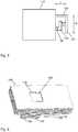
- Fig. 1shows a perspective view illustrating an antenna device 100 which is based on the illustrated concepts.
- the antenna device 100includes a multi-layer PCB 110 and antennas 120, 140 formed in an edge region of the multi-layer PCB 110.
- the multi-layer PCB 110includes multiple PCB layers which are stacked in a vertical direction.
- the PCB layersmay for example each correspond to a structured metallization layer on an isolating substrate.
- the antenna 120is a patch antenna extending in a plane which is perpendicular to the PCB layers and parallel to one of the edges of the multi-layer PCB 110.
- the antenna 140is a dipole antenna formed on one of the PCB layers and extends in a horizontal direction, perpendicular to the vertical direction and along the edge of the multi-layer PCB 110.
- the antenna device 100includes a radio front end circuitry chip 180 which is arranged in a cavity 170 formed in the multi-layer PCB 110. Accordingly, electric connections from the radio front end circuitry chip 180 to the antennas 120, 140 can be efficiently formed by conductive strips on one or more of the PCB layers. In particular, the electric connections may be formed with short lengths, so that signal losses at high frequencies can be limited. Further, one or more of the PCB layers may also be utilized for connecting the radio front end circuitry chip 180 to other circuitry, e.g., to power supply circuitry or digital signal processing circuitry.
- Fig. 2further illustrates structures of the patch antenna 120 and the dipole antenna 140.
- Fig. 2does not show the isolating substrates of the PCB layers in the edge region 115 of the multi-layer PCB 110.
- the patch antenna 120includes an antenna patch 121 which extends in a plane which is perpendicular to the PCB layers and extends along the edge of the multi-layer PCB 110.
- the antenna patch 121is configured for transmission of radio signals with a vertical polarization direction (illustrated by a solid arrow), i.e., a direction perpendicular to the PCB layers.
- the dipole antenna 140includes a first pole formed of a first conductive strip 141 and a second pole formed of a second conductive strip 142.
- the first conductive strip 141 and the second conductive strip 142extend along the edge of the multi-layer PCB 110.
- the dipole antenna 140is configured for transmission of radio signals with a horizontal polarization direction (illustrated by an open arrow), i.e., a direction parallel to the PCB layers and parallel to the edge of the multi-layer PCB 110.
- Fig. 3further illustrates structures of the antenna patch 121. Similar to Fig. 2 , Fig. 3 does not show the isolating substrates of the PCB layers in the edge region 115 of the multi-layer PCB 110.
- the antenna patch 121is formed of multiple conductive strips 121 on different PCB layers.
- the conductive strips 122are stacked above each other in the vertical direction, thereby forming a three-dimensional superstructure.
- the conductive strips 122 of the different PCB layersare connected by conductive vias 123, e.g., metalized via holes.
- the conductive strips 122 and the conductive vias of the antenna patch 121are arranged in a mesh pattern and form a substantially rectangular conductive structure extending the plane perpendicular to the PCB layers and in parallel to the edge of the multi-layer PCB 110.
- the grid spacing of the mesh patternis selected to be sufficiently small so that, at the intended wavelength of the radio signals to be transmitted by the patch antenna 120, differences as compared to a uniform conductive structure are negligible. Typically, this can be achieved by a grid spacing of less than a quarter of the vertical and/or horizontal dimension of the antenna patch 121, e.g., of about 10% of the vertical and/or horizontal dimension of the antenna patch. It is noted that while Fig. 3 shows the mesh pattern with a regular grid structure, utilization of an irregular grid structure, e.g., based on irregular distances of the vias 123 along the conductive strip 122 and/or vias 123 which are not-aligned in the vertical direction, could be utilized as well.
- Fig. 4further illustrates structures of the patch antenna 120. Similar to Figs. 2 and 3, Fig. 4 does not show the isolating substrates of the PCB layers in the edge region 115 of the multi-layer PCB 110.
- the patch antenna 120includes a feeding patch 125.
- the feeding patch 125is configured for capacitive feeding of the antenna patch 121 and extends in parallel to the antenna patch 121, offset therefrom towards the center of the multi-layer PCB 110.
- the feeding patch 125has a smaller size than the antenna patch 121.
- the feeding patch 125is formed of multiple conductive strips 126 on different PCB layers. The conductive strips 126 are stacked above each other in the vertical direction, thereby forming a three-dimensional superstructure.
- the conductive strips 126 of the different PCB layersare connected by conductive vias 127, e.g., metalized via holes.
- the conductive strips 126 and the conductive vias of the feeding patch 125are arranged in a mesh pattern and form a substantially rectangular conductive structure extending the plane perpendicular to the PCB layers and in parallel to the edge of the multi-layer PCB 110.
- the grid spacing of the mesh patternis selected to be sufficiently small so that, at the intended wavelength of the radio signals to be transmitted by the patch antenna 120, differences as compared to a uniform conductive structure are negligible.
- the feeding patch 125may be formed with a similar or the same grid spacing as the antenna patch 121. Similar to the antenna patch 121, the feeding patch 125 may have a regular grid structure or an irregular grid structure.
- the patch antenna 120may be provided with a grounding patch 124 which electrically connects the antenna patch 121 to a groundplane.
- the groundplanecould be formed by a conductive region on one of the PCB layers.
- the grounding patch 124may be formed of a conductive strip formed on one of the PCB layers. As illustrated in Fig. 4 , the grounding patch 124 may be offset from the feeding patch 125 in the vertical direction.
- Fig. 5shows a schematic sectional view for illustrating configuration and dimensioning of the patch antenna 120, i.e., a view in a plane perpendicular to the horizontal direction.
- the feeding patch 125is connected to a feeding point 128. From the feeding point 128, an electrical connection to the radio front end circuitry chip 180 may be formed on one of the PCB layers.
- the feeding patch 125is spaced by a distance G from the antenna patch 121.
- the antenna patchhas a dimension W along the horizontal direction, and the grounding patch 124 has a length L.
- the distance G and the size of the feeding patch 125may be set with the aim of optimizing capacitive coupling to the antenna patch 121.
- the dimension W, the distance G, and the length Lmay be set according to the nominal wavelength of radio signals to be transmitted or received via the patch antenna 120.
- the dimension Wmay correspond to a quarter of the nominal wavelength, and the length L and the distance G may be less than a quarter of the nominal wavelength.
- the patch antennais configured as a half wave patch antenna, the grounding patch 124 is omitted, the dimension W may correspond to half of the nominal wavelength, and the distance G may be less than a quarter of the nominal wavelength.
- Wwhen optimizing the patch antenna 120 for radio signals with a frequency of 14 GHz, W may be about 3 mm and the length L may be less than 3 mm, such as 2 mm.
- WWhen optimizing the patch antenna 120 for radio signals with a frequency of 28 GHz, W may be about 1.5 mm and the length L may be less than 1.5 mm, such as 1 mm. Accordingly, the patch antenna 120 can be built without requiring excessive thickness of the multi-layer PCB 110. In particular, the thickness of the multi-layer PCB 110 may be 5 mm or even less.
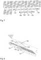
- Fig. 6shows a perspective view illustrating a further antenna device 100' which is based on the illustrated concepts. Structures which are similar to those of Figs. 1 to 5 have been designated with the same reference signs, and details of such structures can also be taken from the above description in connection with Fig. 1 to 5 .
- the antenna device 100'includes a multi-layer PCB 110 and antennas 120, 130, 140 150, formed in an edge region of the multi-layer PCB 110.
- the multi-layer PCB 110includes multiple PCB layers which are stacked in a vertical direction.
- the PCB layersmay for example each correspond to a structured metallization layer on an isolating substrate.
- Fig. 6does not show the isolating substrates of the PCB layers in the edge region 115 of the multi-layer PCB 110.
- the antenna device 100'includes a radio front end circuitry chip 180 which is arranged in a cavity 170 formed in the multi-layer PCB 110. Accordingly, electric connections from the radio front end circuitry chip 180 to the antennas 120, 130, 140, 150 can be efficiently formed by conductive strips on one or more of the PCB layers.
- the antennas 120 and 130are patch antennas extending in a plane which is perpendicular to the PCB layers and parallel to one of the edges of the multi-layer PCB 110.
- the antennas 140, 150are dipole antennas formed on one of the PCB layers and extend in a horizontal direction, perpendicular to the vertical direction and along the edge of the multi-layer PCB 110.
- the patch antennas 120 and 130have different sizes to support transmission in different frequency bands.
- the dipole antennas 140 and 150have different sizes to support transmission in different frequency bands.
- the patch antennas 120, 130are configured for transmission of radio signals with a vertical polarization direction
- the dipole antennas 140are configured for transmission of radio signals with a horizontal polarization direction.
- Fig. 7further illustrates the different dimensioning of the dipole antennas 140, 150.
- the dipole antenna 140includes a first pole formed of a first conductive strip 141 and a second pole formed of a second conductive strip 142.
- the first conductive strip 141 and the second conductive strip 142extend along the edge of the multi-layer PCB 110 and extend over a first length D1.
- the dipole antenna 140includes a first pole formed of a first conductive strip 151 and a second pole formed of a second conductive strip 152.
- the first conductive strip 151 and the second conductive strip 152extend along the edge of the multi-layer PCB 110 and extend over a second length D2.
- the first length D1is higher than the second length D2, i.e., the first dipole antenna 140 is optimized for transmission of radio signals with a longer wavelength than the second dipole antenna 150.
- the first length D1may correspond to half of the nominal wavelength of radio signals in a first frequency band (e.g., in the range of 25 GHz)
- the second length D2may correspond to half of the nominal wavelength of radio signals in a first frequency band (e.g., in the range of 40 GHz).
- the first dipole antenna 140 and the second dipole antenna 150share a common feeding branch formed of conductive strips 161, 162.
- the conductive strip 161is connected to the conductive strips 141 and 151, i.e., feeds the first poles of the dipole antennas 140, 150.
- the conductive strip 162is connected to the conductive strips 142 and 152, i.e., feeds the second poles of the dipole antennas 140, 150.
- Fig. 8further illustrates structures of the patch antennas 120, 130.
- the first patch antenna 120includes an antenna patch 121.
- the antenna patch 121is formed of multiple conductive strips on different PCB layers which are connected to each other by conductive vias.
- the second patch antenna 130includes an antenna patch 131 formed of multiple conductive strips 132 on different PCB layers.
- the conductive strips 132are stacked above each other in the vertical direction, thereby forming a three-dimensional superstructure.
- the conductive strips 132 of the different PCB layersare connected by conductive vias 133, e.g., metalized via holes.
- the conductive strips 132 and the conductive vias of the antenna patch 131are arranged in a mesh pattern and form a substantially rectangular conductive structure extending the plane perpendicular to the PCB layers and in parallel to the edge of the multi-layer PCB 110.
- the antenna patch 131may be formed with a similar or the same grid spacing as the antenna patch 121. Similar to the antenna patch 121, the antenna patch 131 may have a regular grid structure or an irregular grid structure.
- the first patch antenna 120 and the second patch antenna 130have different sizes to support different wavelengths.
- the patch antenna 120may have a higher vertical dimension than the patch antenna 130.
- the vertical dimension W of the antenna patch 121 of the first patch antenna 120may correspond to half of the nominal wavelength of radio signals in a first frequency band (e.g., in the range of 25 GHz)
- the vertical dimension W of the antenna patch 131 of the second patch antenna 130may correspond to half of the nominal wavelength of radio signals in a first frequency band (e.g., in the range of 40 GHz).
- the patch antenna 120 and the second patch antenna 130share a common feeding branch 136.
- the common feeding branch 136is formed of a conductive strip on one of the PCB layers and connects to a first feeding patch 125 extending in the vertical direction and configured for capacitive feeding of the antenna patch 121.
- the feeding patch 125may be formed of conductive strips on different PCB layers which are vertically connected by conductive vias.
- the common feeding branch 136connects to a second feeding patch 135 extending in the vertical direction and configured for capacitive feeding of the antenna patch 131.
- the second feeding patch 135may be formed of conductive strips on different PCB layers which are vertically connected by conductive vias.
- the corresponding feeding patches 125, 135may be configured with different sizes.
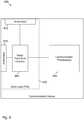
- Fig. 9schematically illustrates a communication device 900 which is equipped with an antenna device as explained above, e.g., with the antenna device 100 or the antenna device 100'.
- the communication devicemay correspond to a small sized user device, e.g., a mobile phone, a smartphone, a tablet computer, or the like.
- a small sized user devicee.g., a mobile phone, a smartphone, a tablet computer, or the like.
- vehicle based communication devicese.g., vehicle based communication devices, wireless modems, or autonomous sensors.
- the communication device 900includes one or more antennas 910. These antennas 910 include at least one antenna of the above-mentioned patch antenna type, such as the patch antenna 120 or the patch antenna 130. Further, the communication device 900 may also include other kinds of antennas, such as the above-mentioned dipole antennas 140, 150, or even other antenna types. Using concepts as explained above, the antennas 910 are integrated together with radio front end circuitry 920 on a multi-layer PCB 930. As further illustrated, the communication device 900 also includes one or more communication processor(s) 940. The communication processor(s) 940 may generate or otherwise process communication signals for transmission via the antennas 910. For this purpose, the communication processor(s) 940 may perform various kinds of signal processing and data processing according to one or more communication protocols, e.g., in accordance with a 5G cellular radio technology.
- the concepts as explained aboveare susceptible to various modifications.
- the conceptscould be applied in connection with various kinds of radio technologies and communication devices, without limitation to a 5G technology.
- the illustrated antennasmay be used for transmitting radio signals from a communication device and/or for receiving radio signals in a communication device.
- the illustrated antenna structuresmay be subjected to various modifications concerning antenna geometry.
- the illustrated rectangular antenna patch shapescould be modified to more complex shapes.
Landscapes
- Physics & Mathematics (AREA)
- Electromagnetism (AREA)
- Waveguide Aerials (AREA)
- Details Of Aerials (AREA)
- Variable-Direction Aerials And Aerial Arrays (AREA)
Description
- The present invention relates to antennas, antenna devices with one or more antennas and communication devices equipped with such antenna device.
- In wireless communication technologies, various frequency bands are utilized for conveying communication signals. In order to meet increasing bandwidth demands, also frequency bands in the millimeter wavelength range, corresponding to frequencies in the range of about 10 GHz to about 100 GHz, are considered. For example, frequency bands in the millimeter wavelength range are considered as candidates for 5G (5th Generation) cellular radio technologies. However, an issue which arises with the utilization of such high frequencies is that antenna sizes need to be sufficiently small to match the wavelength. Further, in order to achieve sufficient performance, multiple antennas (e.g., in the form of an antenna array) may be needed in small sized communication devices, such as mobile phones, smartphones, or similar communication devices.
- Further, since losses on cables or other wired connections within the communication device typically increase towards higher frequencies, it may also be desirable to have an antenna design in which the antenna can be placed very close to radio front end circuitry.
- Accordingly, there is a need for compact size antennas which can be efficiently integrated in a communication device.
US 2013/0207869 A1 describes a side-face radiation antenna including a patch part formed by metal filled in a plurality of vias connecting layers of a substrate. The antenna is fed by a feed line part.US 6,943,735 B1 describes an antenna having a radiating part which is composed, in part, of a grid of electrically conductive layers and vias.US 2016/0087348 A1 describes a horizontal polarization antenna having a radiator formed by a mesh-grid structure in a multi-layer circuit board.- According to an embodiment, a device is provided. The device comprises at least one antenna and a multi-layer printed circuit board (PCB). The multi-layer PCB has multiple layers stacked along a vertical direction. The device may for example correspond to an antenna module including multiple antennas. Further, the device may correspond to an antenna circuit package including one or more antennas and radio front end circuitry for feeding radio frequency signals to the antenna(s). The at least one antenna comprises an antenna patch and a feeding patch configured for capacitive feeding of the antenna patch. The antenna patch is formed of multiple conductive strips extending in a horizontal direction along an edge of the multi-layer PCB. Each of the conductive strips of the antenna patch is arranged on a different layer of the multi-layer PCB. The conductive strips are electrically connected to each other by conductive vias extending between two or more of the conductive strips of the antenna patch, which are arranged on different layers of the multi-layer PCB. The feeding patch is formed of multiple conductive strips extending in the horizontal direction. Each of the conductive strips of the feeding patch is arranged on a different layer of the multi-layer PCB. The conductive strips of the feeding patch are electrically connected to each other by conductive vias extending between two or more of the conductive strips of the feeding patch, which are arranged on different layers of the multi-layer PCB.
- According to an embodiment, the conductive strips and the conductive vias of the antenna patch are arranged to form a mesh pattern. For example, the conductive strips and the conductive vias of the antenna patch may form a regular grid extending in a plane defined by the horizontal direction and the vertical direction.
- Similarly, the conductive strips and the conductive vias of the feeding patch may be arranged to form a mesh pattern. For example, the conductive strips and the conductive vias of the antenna patch may form a regular grid extending in a plane defined by the horizontal direction and the vertical direction, parallel to a plane in which the antenna patch extends.
- In the vertical and the horizontal direction, the feeding patch may have a dimension which is shorter than a quarter wavelength of a radio signal to be transmitted via the antenna. For example, a vertical dimension of the antenna patch may be in the range of 0,2 mm to 8 mm. Similarly, a horizontal dimension of the antenna patch may be in the range of 0,2 mm to 8 mm.
- According to an embodiment, the at least one antenna further comprises a grounding patch which conductively connects the antenna patch to a groundplane. The groundplane may be formed by one or more conductive regions of one or more layers of the multi-layer PCB.
- According to an embodiment, the grounding patch has a length which is shorter than a quarter wavelength of a radio signal to be transmitted via the antenna. For example, the length of the grounding patch may be in the range of 0,2 mm to 8 mm.
- According to an embodiment, the at least one antenna is configured for transmission of radio signals having a wavelength of more than 1 mm and less than 3 cm, corresponding to frequencies of the radio signals in the range of 10 GHz to 300 GHz.
- According to an embodiment, the device may comprise radio front end circuitry arranged on the multi-layer PCB. The radio front end circuitry may for example include one or more amplifiers and/or one or more modulators for processing radio signals transmitted via the antennas.
- According to an embodiment, the device comprises a first antenna and a second antenna each having a configuration as defined in any one of the above embodiments, and the antenna patch of the first antenna has a different size than the antenna patch of the second antenna. In this way, the first antenna and the second antenna may efficiently support transmission of radio signals from two different frequency bands.
- According to an embodiment, the feeding patch of the first antenna and the feeding patch of the second antenna are connected to a common feeding branch formed by a conductive strip on one of the layers of the multi-layer PCB.
- According to an embodiment, the device further comprises at least one dipole antenna formed by conductive strips on one or more of the layers of the multi-layer printed circuit board, e.g., conductive strips extending along the horizontal direction.
- According to an embodiment, the device comprises a first dipole antenna formed by conductive strips on one of the layers of the multi-layer PCB and a second dipole antenna formed by conductive strips on this one layer of the multi-layer PCB, and the conductive strips of the first dipole antenna have a different size than the conductive strips of the second dipole antenna. In this way, the first dipole antenna and the second dipole antenna may efficiently support transmission of radio signals from two different frequency bands.
- According to an embodiment, the first dipole antenna and the second dipole antenna are connected to a common feeding branch formed by conductive strips on the one layer of the multi-layer PCB.
- If the device includes radio front end circuitry arranged on the multi-layer PCB, the multi-layer PCB may comprise a cavity in which the radio front end circuitry is received.
- According to a further embodiment, a communication device is provided, e.g., in the form of a mobile phone, smartphone or similar user device. The communication device comprises a device according to any one of the above embodiments, i.e., a device including at least one antenna having a configuration as defined in any one of the above embodiments and the multi-layer PCB. Further, the communication device comprises at least one processor configured to process communication signals transmitted via the at least one antenna of the device.
- The above and further embodiments of the invention will now be described in more detail with reference to the accompanying drawings.
Fig. 1 shows a perspective view schematically illustrating an antenna device according to an embodiment of the invention.Fig. 2 shows a further perspective view for illustrating antennas of the antenna device.Figs. 3 shows a perspective view for schematically illustrating an antenna patch of the antenna device.Fig. 4 shows a perspective view for schematically illustrating a feeding patch of the antenna device.Fig. 5 shows a sectional view schematically illustrating configuration and dimensioning of a patch antenna of the antenna device.Fig. 6 shows a perspective view schematically illustrating an antenna device according to a further embodiment of the invention.Fig. 7 shows a perspective view schematically illustrating dimensioning of different antennas of the antenna device.Fig. 8 shows a perspective view schematically illustrating capacitive feeding of different antennas of the antenna device.Fig. 9 shows a block diagram for schematically illustrating a communication device according to an embodiment of the invention.- In the following, exemplary embodiments of the invention will be described in more detail. It has to be understood that the following description is given only for the purpose of illustrating the principles of the invention and is not to be taken in a limiting sense. Rather, the scope of the invention is defined only by the appended claims and is not intended to be limited by the exemplary embodiments described hereinafter.
- The illustrated embodiments relate to antennas for transmission of radio signals, in particular of short wavelength radio signals in the cm/mm wavelength range. The illustrated antennas and antenna devices may for example be utilized in communication devices, such as a mobile phone, smartphone, tablet computer, or the like.
- In the illustrated concepts, a multi-layer PCB is utilized for forming a C-fed (capacitively fed) patch antenna. The multi-layer PCB has multiple layers stacked in a vertical direction. The layers of the multi-layer PCB may be individually structured with patterns of conductive strips. In particular, conductive strips formed on different layers of the multi-layer PCB may be connected to each other by conductive vias extending between the conductive strips of different layers to form an antenna patch and a feeding patch which is capacitively coupled to the antenna patch. The patch antenna may be of a quarter-wave type or of a half-wave type. In this way, the antenna patch and the feeding patch may be formed to extend in the vertical direction, perpendicular to the planes of the layers of the multi-layer PCB. In this way, an antenna allowing for transmission of radio signals polarized in the vertical direction may be formed in an efficient manner. Further, one or more layers of the multi-layer PCB may be utilized in an efficient manner for connecting the patch antenna to radio front end circuitry. Specifically, a small size of the patch antenna and short lengths of connections to the patch antenna may be achieved. Further, it is possible to integrate a plurality of such patch antennas on the multi-layer PCB. Moreover, the patch antenna(s) can be efficiently combined with other antenna types formed on one or more layers of the multi-layer PCB. In this way, different polarization directions and/or different frequency bands may be supported in a compact structure.
Fig. 1 shows a perspective view illustrating anantenna device 100 which is based on the illustrated concepts. In the illustrated example, theantenna device 100 includes amulti-layer PCB 110 andantennas multi-layer PCB 110. Themulti-layer PCB 110 includes multiple PCB layers which are stacked in a vertical direction. The PCB layers may for example each correspond to a structured metallization layer on an isolating substrate. Theantenna 120 is a patch antenna extending in a plane which is perpendicular to the PCB layers and parallel to one of the edges of themulti-layer PCB 110. Theantenna 140 is a dipole antenna formed on one of the PCB layers and extends in a horizontal direction, perpendicular to the vertical direction and along the edge of themulti-layer PCB 110.- Further, the
antenna device 100 includes a radio frontend circuitry chip 180 which is arranged in acavity 170 formed in themulti-layer PCB 110. Accordingly, electric connections from the radio frontend circuitry chip 180 to theantennas end circuitry chip 180 to other circuitry, e.g., to power supply circuitry or digital signal processing circuitry. Fig. 2 further illustrates structures of thepatch antenna 120 and thedipole antenna 140. For this purpose,Fig. 2 does not show the isolating substrates of the PCB layers in theedge region 115 of themulti-layer PCB 110.- As can be seen, the
patch antenna 120 includes anantenna patch 121 which extends in a plane which is perpendicular to the PCB layers and extends along the edge of themulti-layer PCB 110. Theantenna patch 121 is configured for transmission of radio signals with a vertical polarization direction (illustrated by a solid arrow), i.e., a direction perpendicular to the PCB layers. Thedipole antenna 140 includes a first pole formed of a firstconductive strip 141 and a second pole formed of a secondconductive strip 142. The firstconductive strip 141 and the secondconductive strip 142 extend along the edge of themulti-layer PCB 110. Thedipole antenna 140 is configured for transmission of radio signals with a horizontal polarization direction (illustrated by an open arrow), i.e., a direction parallel to the PCB layers and parallel to the edge of themulti-layer PCB 110. Fig. 3 further illustrates structures of theantenna patch 121. Similar toFig. 2 ,Fig. 3 does not show the isolating substrates of the PCB layers in theedge region 115 of themulti-layer PCB 110.- As can be seen, the
antenna patch 121 is formed of multipleconductive strips 121 on different PCB layers. Theconductive strips 122 are stacked above each other in the vertical direction, thereby forming a three-dimensional superstructure. Theconductive strips 122 of the different PCB layers are connected byconductive vias 123, e.g., metalized via holes. As illustrated, theconductive strips 122 and the conductive vias of theantenna patch 121 are arranged in a mesh pattern and form a substantially rectangular conductive structure extending the plane perpendicular to the PCB layers and in parallel to the edge of themulti-layer PCB 110. The grid spacing of the mesh pattern is selected to be sufficiently small so that, at the intended wavelength of the radio signals to be transmitted by thepatch antenna 120, differences as compared to a uniform conductive structure are negligible. Typically, this can be achieved by a grid spacing of less than a quarter of the vertical and/or horizontal dimension of theantenna patch 121, e.g., of about 10% of the vertical and/or horizontal dimension of the antenna patch. It is noted that whileFig. 3 shows the mesh pattern with a regular grid structure, utilization of an irregular grid structure, e.g., based on irregular distances of thevias 123 along theconductive strip 122 and/orvias 123 which are not-aligned in the vertical direction, could be utilized as well. Fig. 4 further illustrates structures of thepatch antenna 120. Similar toFigs. 2 and3, Fig. 4 does not show the isolating substrates of the PCB layers in theedge region 115 of themulti-layer PCB 110.- As can be seen, in addition to the
antenna patch 121, thepatch antenna 120 includes afeeding patch 125. Thefeeding patch 125 is configured for capacitive feeding of theantenna patch 121 and extends in parallel to theantenna patch 121, offset therefrom towards the center of themulti-layer PCB 110. Thefeeding patch 125 has a smaller size than theantenna patch 121. Similar to theantenna patch 121, thefeeding patch 125 is formed of multipleconductive strips 126 on different PCB layers. Theconductive strips 126 are stacked above each other in the vertical direction, thereby forming a three-dimensional superstructure. Theconductive strips 126 of the different PCB layers are connected byconductive vias 127, e.g., metalized via holes. As illustrated, theconductive strips 126 and the conductive vias of thefeeding patch 125 are arranged in a mesh pattern and form a substantially rectangular conductive structure extending the plane perpendicular to the PCB layers and in parallel to the edge of themulti-layer PCB 110. The grid spacing of the mesh pattern is selected to be sufficiently small so that, at the intended wavelength of the radio signals to be transmitted by thepatch antenna 120, differences as compared to a uniform conductive structure are negligible. Accordingly, thefeeding patch 125 may be formed with a similar or the same grid spacing as theantenna patch 121. Similar to theantenna patch 121, thefeeding patch 125 may have a regular grid structure or an irregular grid structure. - As further illustrated in
Fig. 4 , thepatch antenna 120 may be provided with agrounding patch 124 which electrically connects theantenna patch 121 to a groundplane. The groundplane could be formed by a conductive region on one of the PCB layers. Thegrounding patch 124 may be formed of a conductive strip formed on one of the PCB layers. As illustrated inFig. 4 , thegrounding patch 124 may be offset from thefeeding patch 125 in the vertical direction. Fig. 5 shows a schematic sectional view for illustrating configuration and dimensioning of thepatch antenna 120, i.e., a view in a plane perpendicular to the horizontal direction. As can be seen, thefeeding patch 125 is connected to afeeding point 128. From thefeeding point 128, an electrical connection to the radio frontend circuitry chip 180 may be formed on one of the PCB layers. Thefeeding patch 125 is spaced by a distance G from theantenna patch 121. The antenna patch has a dimension W along the horizontal direction, and thegrounding patch 124 has a length L. The distance G and the size of thefeeding patch 125 may be set with the aim of optimizing capacitive coupling to theantenna patch 121. Simulations have shown that a smallsized feeding patch 125, e.g., having a quarter or less of the size of theantenna patch 121, allows for achieving a good bandwidth, a compact overall size of thepatch antenna 120, and an almost uniform omnidirectional transmission characteristic.- Further, the dimension W, the distance G, and the length L may be set according to the nominal wavelength of radio signals to be transmitted or received via the
patch antenna 120. As a general rule, when assuming a configuration of thepatch antenna 120 as a quarter wave patch antenna, the dimension W may correspond to a quarter of the nominal wavelength, and the length L and the distance G may be less than a quarter of the nominal wavelength. If the patch antenna is configured as a half wave patch antenna, thegrounding patch 124 is omitted, the dimension W may correspond to half of the nominal wavelength, and the distance G may be less than a quarter of the nominal wavelength. - For example, when optimizing the
patch antenna 120 for radio signals with a frequency of 14 GHz, W may be about 3 mm and the length L may be less than 3 mm, such as 2 mm. When optimizing thepatch antenna 120 for radio signals with a frequency of 28 GHz, W may be about 1.5 mm and the length L may be less than 1.5 mm, such as 1 mm. Accordingly, thepatch antenna 120 can be built without requiring excessive thickness of themulti-layer PCB 110. In particular, the thickness of themulti-layer PCB 110 may be 5 mm or even less. Fig. 6 shows a perspective view illustrating a further antenna device 100' which is based on the illustrated concepts. Structures which are similar to those ofFigs. 1 to 5 have been designated with the same reference signs, and details of such structures can also be taken from the above description in connection withFig. 1 to 5 .- As illustrated, the antenna device 100' includes a
multi-layer PCB 110 andantennas multi-layer PCB 110. Themulti-layer PCB 110 includes multiple PCB layers which are stacked in a vertical direction. The PCB layers may for example each correspond to a structured metallization layer on an isolating substrate. For illustrative purposes,Fig. 6 does not show the isolating substrates of the PCB layers in theedge region 115 of themulti-layer PCB 110. Further, the antenna device 100' includes a radio frontend circuitry chip 180 which is arranged in acavity 170 formed in themulti-layer PCB 110. Accordingly, electric connections from the radio frontend circuitry chip 180 to theantennas - The
antennas multi-layer PCB 110. Theantennas multi-layer PCB 110. As can be seen, thepatch antennas dipole antennas patch antennas dipole antennas 140, are configured for transmission of radio signals with a horizontal polarization direction. Fig. 7 further illustrates the different dimensioning of thedipole antennas dipole antenna 140 includes a first pole formed of a firstconductive strip 141 and a second pole formed of a secondconductive strip 142. The firstconductive strip 141 and the secondconductive strip 142 extend along the edge of themulti-layer PCB 110 and extend over a first length D1. Thedipole antenna 140 includes a first pole formed of a firstconductive strip 151 and a second pole formed of a secondconductive strip 152. The firstconductive strip 151 and the secondconductive strip 152 extend along the edge of themulti-layer PCB 110 and extend over a second length D2. The first length D1 is higher than the second length D2, i.e., thefirst dipole antenna 140 is optimized for transmission of radio signals with a longer wavelength than thesecond dipole antenna 150. For example, the first length D1 may correspond to half of the nominal wavelength of radio signals in a first frequency band (e.g., in the range of 25 GHz), and the second length D2 may correspond to half of the nominal wavelength of radio signals in a first frequency band (e.g., in the range of 40 GHz).- As further shown in
Fig. 7 , thefirst dipole antenna 140 and thesecond dipole antenna 150 share a common feeding branch formed ofconductive strips conductive strip 161 is connected to theconductive strips dipole antennas conductive strip 162 is connected to theconductive strips dipole antennas Fig. 8 further illustrates structures of thepatch antennas first patch antenna 120 includes anantenna patch 121. As explained in connection withFig. 3 , theantenna patch 121 is formed of multiple conductive strips on different PCB layers which are connected to each other by conductive vias. Similarly, thesecond patch antenna 130 includes anantenna patch 131 formed of multipleconductive strips 132 on different PCB layers. Theconductive strips 132 are stacked above each other in the vertical direction, thereby forming a three-dimensional superstructure. Theconductive strips 132 of the different PCB layers are connected byconductive vias 133, e.g., metalized via holes. As illustrated, theconductive strips 132 and the conductive vias of theantenna patch 131 are arranged in a mesh pattern and form a substantially rectangular conductive structure extending the plane perpendicular to the PCB layers and in parallel to the edge of themulti-layer PCB 110. Theantenna patch 131 may be formed with a similar or the same grid spacing as theantenna patch 121. Similar to theantenna patch 121, theantenna patch 131 may have a regular grid structure or an irregular grid structure.- As mentioned above, the
first patch antenna 120 and thesecond patch antenna 130 have different sizes to support different wavelengths. For example, when designating the vertical dimension with W (as in the illustration ofFig. 5 ), thepatch antenna 120 may have a higher vertical dimension than thepatch antenna 130. For example, when assuming a configuration as half wave patch antennas, the vertical dimension W of theantenna patch 121 of thefirst patch antenna 120 may correspond to half of the nominal wavelength of radio signals in a first frequency band (e.g., in the range of 25 GHz), and the vertical dimension W of theantenna patch 131 of thesecond patch antenna 130 may correspond to half of the nominal wavelength of radio signals in a first frequency band (e.g., in the range of 40 GHz). - As further shown in
Fig. 8 , thepatch antenna 120 and thesecond patch antenna 130 share acommon feeding branch 136. Thecommon feeding branch 136 is formed of a conductive strip on one of the PCB layers and connects to afirst feeding patch 125 extending in the vertical direction and configured for capacitive feeding of theantenna patch 121. As explained in connection withFig. 4 , thefeeding patch 125 may be formed of conductive strips on different PCB layers which are vertically connected by conductive vias. Further, thecommon feeding branch 136 connects to asecond feeding patch 135 extending in the vertical direction and configured for capacitive feeding of theantenna patch 131. Similar to thefirst feeding patch 125, thesecond feeding patch 135 may be formed of conductive strips on different PCB layers which are vertically connected by conductive vias. In accordance with the differentlysized antenna patches corresponding feeding patches Fig. 9 schematically illustrates acommunication device 900 which is equipped with an antenna device as explained above, e.g., with theantenna device 100 or the antenna device 100'. The communication device may correspond to a small sized user device, e.g., a mobile phone, a smartphone, a tablet computer, or the like. However, it is to be understood that other kinds of communication devices could be used as well, e.g., vehicle based communication devices, wireless modems, or autonomous sensors.- As illustrated, the
communication device 900 includes one ormore antennas 910. Theseantennas 910 include at least one antenna of the above-mentioned patch antenna type, such as thepatch antenna 120 or thepatch antenna 130. Further, thecommunication device 900 may also include other kinds of antennas, such as the above-mentioneddipole antennas antennas 910 are integrated together with radiofront end circuitry 920 on amulti-layer PCB 930. As further illustrated, thecommunication device 900 also includes one or more communication processor(s) 940. The communication processor(s) 940 may generate or otherwise process communication signals for transmission via theantennas 910. For this purpose, the communication processor(s) 940 may perform various kinds of signal processing and data processing according to one or more communication protocols, e.g., in accordance with a 5G cellular radio technology. - It is to be understood that the concepts as explained above are susceptible to various modifications. For example, the concepts could be applied in connection with various kinds of radio technologies and communication devices, without limitation to a 5G technology. The illustrated antennas may be used for transmitting radio signals from a communication device and/or for receiving radio signals in a communication device. Further, it is to be understood that the illustrated antenna structures may be subjected to various modifications concerning antenna geometry. For example, the illustrated rectangular antenna patch shapes could be modified to more complex shapes.
Claims (15)
- A device (100; 100'), comprising:at least one antenna (120, 130; 910);a multi-layer printed circuit board (110) having multiple layers stacked along a vertical direction;wherein the at least one antenna (120, 130; 910) comprises:an antenna patch (121, 131); anda feeding patch (125, 135) configured for capacitive feeding of the antenna patch (121, 131),the antenna patch (121, 131) being formed of multiple conductive strips (122, 132) extending in a horizontal direction along an edge of the multi-layer printed circuit board (110),each of the conductive strips (122, 132) of the antenna patch being arranged on a different layer of the multi-layer printed circuit board (110),the conductive strips (122, 132) being electrically connected to each other by conductive vias (123, 133) extending between two or more of the conductive strips (122, 132) of the antenna patch, which are arranged on different layers of the multi-layer printed circuit board (110),the feeding patch (125, 135) being formed of multiple conductive strips (126) extending in the horizontal direction, each of the conductive strips (126) of the feeding patch (125, 135) being arranged on a different layer of the multi-layer printed circuit board, andthe conductive strips (126) of the feeding patch being electrically connected to each other by conductive vias (127) extending between two or more of the conductive strips (126) of the feeding patch (125, 135), which are arranged on different layers of the multi-layer printed circuit board (110).
- The device (100; 100') according to claim 1,
wherein the conductive strips (122, 132) and the conductive vias (123, 133) of the antenna patch are arranged to form a mesh pattern. - The device (100; 100') according to claim 1 or 2,
wherein the conductive strips (126) and the conductive vias (127) of the feeding patch are arranged to form a mesh pattern. - The antenna device (100; 100') according to any one of the preceding claims,
wherein, in the vertical and the horizontal direction, the feeding patch has a dimension which is shorter than a quarter wavelength of a radio signal to be transmitted via the antenna. - The device (100; 100') according to any one of the preceding claims,
wherein the at least one antenna (120, 130, 910) further comprises: - a grounding patch (124) which conductively connects the antenna patch (121) to a groundplane. - The device (100; 100') according to claim 5,
wherein the grounding patch (124) has a length which is shorter than a quarter wavelength of a radio signal to be transmitted via the antenna (120, 130). - The device (100; 100')according to any one of the preceding claims,
wherein the at least one antenna (120, 130, 910) is configured for transmission of radio signals having a wavelength of more than 1 mm and less than 3 cm. - The device (100') according to any one of the preceding claims,
wherein the at least one antenna (120, 130; 910) comprises a first antenna (120, 130) and
a second antenna (120, 130);
wherein the antenna patch (121, 131) of the first antenna (120, 130) has a different size than the antenna patch (121, 131) of the second antenna (120, 130). - The device (100') according to claim 8,
wherein the feeding patch (125, 135) of the first antenna (120, 130) and the feeding patch (125, 135) of the second antenna (120, 130) are connected to a common feeding branch (136) formed by a conductive strip on one of the layers of the multi-layer printed circuit board (110; 930). - The device (100; 100') according to any one of the preceding claims, comprising:
at least one dipole antenna (140, 150) formed by conductive strips (141, 142, 151, 152) on one or more of the layers of the multi-layer printed circuit board (110; 930). - The device (100') according to claim 10, comprising:a first dipole antenna (140, 150) formed by conductive strips on one of the layers of the multi-layer printed circuit board (110), anda second dipole antenna (140,150) formed by conductive strips (141, 142, 151, 152) on said one layer of the multi-layer printed circuit board (110; 930);wherein the conductive strips (141, 142, 151, 152) of the first dipole antenna (140, 150) have a different size than the conductive strips (141, 142, 151, 152) of the second dipole antenna (140, 150).
- The device according to claim 11,
wherein the first dipole antenna (140, 150) and the second dipole antenna (140, 150) are connected to a common feeding branch formed by conductive strips (161, 162) on said one layer of the multi-layer printed circuit board (110; 930). - The device (100; 100') according to any one of the preceding claims, comprising:
radio front end circuitry (180; 920) arranged on the multi-layer printed circuit board (110; 930). - The device (100; 100') according to claim 13,
wherein the multi-layer printed circuit board (110; 930) comprises a cavity (170) in which the radio front end circuitry (180; 920) is received. - A communication device (900), comprising:a device (100; 100') according to any one of the preceding claims; andat least one processor (940) configured to process communication signals transmitted via the at least one antenna (120, 130; 910) of the device (100).
Applications Claiming Priority (1)
| Application Number | Priority Date | Filing Date | Title |
|---|---|---|---|
| PCT/EP2016/060427WO2017194096A1 (en) | 2016-05-10 | 2016-05-10 | C-fed antenna formed on multi-layer printed circuit board edge |
Publications (2)
| Publication Number | Publication Date |
|---|---|
| EP3455907A1 EP3455907A1 (en) | 2019-03-20 |
| EP3455907B1true EP3455907B1 (en) | 2020-06-24 |
Family
ID=56026830
Family Applications (1)
| Application Number | Title | Priority Date | Filing Date |
|---|---|---|---|
| EP16723988.8AActiveEP3455907B1 (en) | 2016-05-10 | 2016-05-10 | C-fed antenna formed on multi-layer printed circuit board edge |
Country Status (4)
| Country | Link |
|---|---|
| US (1) | US11177573B2 (en) |
| EP (1) | EP3455907B1 (en) |
| CN (1) | CN109155464B (en) |
| WO (1) | WO2017194096A1 (en) |
Families Citing this family (4)
| Publication number | Priority date | Publication date | Assignee | Title |
|---|---|---|---|---|
| US10965030B2 (en)* | 2018-04-30 | 2021-03-30 | Samsung Electro-Mechanics Co., Ltd. | Antenna apparatus |
| FR3083419B1 (en)* | 2018-06-27 | 2022-03-11 | Centre Nat Rech Scient | PRINTED CIRCUIT FOR DATA COMMUNICATION |
| CN111244610B (en)* | 2018-11-29 | 2024-05-24 | 三星电机株式会社 | Antenna device |
| EP3793023A1 (en) | 2019-09-11 | 2021-03-17 | Imst Gmbh | Multilayer printed circuit board including an antenna element, and manufacturing method of a multilayer printed circuit board antenna element |
Family Cites Families (8)
| Publication number | Priority date | Publication date | Assignee | Title |
|---|---|---|---|---|
| US7095382B2 (en)* | 2003-11-24 | 2006-08-22 | Sandbridge Technologies, Inc. | Modified printed dipole antennas for wireless multi-band communications systems |
| US6943735B1 (en) | 2004-02-20 | 2005-09-13 | Lockheed Martin Corporation | Antenna with layered ground plane |
| US7893878B2 (en)* | 2006-12-29 | 2011-02-22 | Broadcom Corporation | Integrated circuit antenna structure |
| US8766867B2 (en)* | 2010-12-16 | 2014-07-01 | Sony Corporation | Compact antenna for multiple input multiple output communications including isolated antenna elements |
| KR20130076291A (en) | 2011-12-28 | 2013-07-08 | 삼성전기주식회사 | Side radiation antenna and wireless telecommunication module |
| US8779564B1 (en) | 2013-03-14 | 2014-07-15 | Intel IP Corporation | Semiconductor device with capacitive coupling structure |
| KR102138909B1 (en)* | 2014-09-19 | 2020-07-28 | 삼성전자주식회사 | Antenna device and method for operation of the same |
| KR102414328B1 (en)* | 2015-09-09 | 2022-06-29 | 삼성전자주식회사 | Antenna device and electronic device including the same |
- 2016
- 2016-05-10WOPCT/EP2016/060427patent/WO2017194096A1/ennot_activeCeased
- 2016-05-10USUS16/099,979patent/US11177573B2/enactiveActive
- 2016-05-10EPEP16723988.8Apatent/EP3455907B1/enactiveActive
- 2016-05-10CNCN201680085555.8Apatent/CN109155464B/enactiveActive
Non-Patent Citations (1)
| Title |
|---|
| None* |
Also Published As
| Publication number | Publication date |
|---|---|
| CN109155464A (en) | 2019-01-04 |
| CN109155464B (en) | 2020-10-02 |
| WO2017194096A1 (en) | 2017-11-16 |
| US11177573B2 (en) | 2021-11-16 |
| EP3455907A1 (en) | 2019-03-20 |
| US20200313300A1 (en) | 2020-10-01 |
Similar Documents
| Publication | Publication Date | Title |
|---|---|---|
| US11145993B2 (en) | Antenna module and terminal thereof | |
| US10461401B2 (en) | Antenna device and electronic device including the same | |
| US10651557B2 (en) | C-fed antenna formed on multi-layer printed circuit board edge | |
| US9590304B2 (en) | Broadband antenna | |
| US11962099B2 (en) | Antenna structure and high-frequency multi-band wireless communication terminal | |
| CN105612660B (en) | A common aperture antenna and base station | |
| EP3301757A1 (en) | Patch antenna element and method for manufacturing a patch antenna element | |
| CN106575815A (en) | Antenna apparatus in wireless communication device | |
| CN108448239A (en) | A millimeter wave antenna array and mobile terminal | |
| CN106463830A (en) | Antenna device | |
| US10862212B2 (en) | Antenna device and wireless communication device | |
| EP3905435B1 (en) | Antenna structure and terminal | |
| CN111527646A (en) | Antenna array and antenna module | |
| EP3455907B1 (en) | C-fed antenna formed on multi-layer printed circuit board edge | |
| KR20160069484A (en) | An assembly of circuit boards and electronic device comprising said assembly | |
| CN112582787B (en) | An antenna structure and electronic device | |
| US10727596B2 (en) | Antenna structure | |
| JP2017092644A (en) | Patch antenna | |
| US11005156B2 (en) | Antenna on protrusion of multi-layer ceramic-based structure | |
| CN209496992U (en) | terminal | |
| KR20050075966A (en) | Omnidirectional antenna | |
| US11901647B2 (en) | Antenna device | |
| KR20170114895A (en) | High Sensitivity Receiver Antenna for Mobile Device |
Legal Events
| Date | Code | Title | Description |
|---|---|---|---|
| STAA | Information on the status of an ep patent application or granted ep patent | Free format text:STATUS: THE INTERNATIONAL PUBLICATION HAS BEEN MADE | |
| PUAI | Public reference made under article 153(3) epc to a published international application that has entered the european phase | Free format text:ORIGINAL CODE: 0009012 | |
| STAA | Information on the status of an ep patent application or granted ep patent | Free format text:STATUS: REQUEST FOR EXAMINATION WAS MADE | |
| 17P | Request for examination filed | Effective date:20181210 | |
| AK | Designated contracting states | Kind code of ref document:A1 Designated state(s):AL AT BE BG CH CY CZ DE DK EE ES FI FR GB GR HR HU IE IS IT LI LT LU LV MC MK MT NL NO PL PT RO RS SE SI SK SM TR | |
| AX | Request for extension of the european patent | Extension state:BA ME | |
| DAV | Request for validation of the european patent (deleted) | ||
| DAX | Request for extension of the european patent (deleted) | ||
| GRAP | Despatch of communication of intention to grant a patent | Free format text:ORIGINAL CODE: EPIDOSNIGR1 | |
| STAA | Information on the status of an ep patent application or granted ep patent | Free format text:STATUS: GRANT OF PATENT IS INTENDED | |
| INTG | Intention to grant announced | Effective date:20200103 | |
| GRAS | Grant fee paid | Free format text:ORIGINAL CODE: EPIDOSNIGR3 | |
| GRAA | (expected) grant | Free format text:ORIGINAL CODE: 0009210 | |
| STAA | Information on the status of an ep patent application or granted ep patent | Free format text:STATUS: THE PATENT HAS BEEN GRANTED | |
| AK | Designated contracting states | Kind code of ref document:B1 Designated state(s):AL AT BE BG CH CY CZ DE DK EE ES FI FR GB GR HR HU IE IS IT LI LT LU LV MC MK MT NL NO PL PT RO RS SE SI SK SM TR | |
| REG | Reference to a national code | Ref country code:GB Ref legal event code:FG4D | |
| REG | Reference to a national code | Ref country code:CH Ref legal event code:EP | |
| REG | Reference to a national code | Ref country code:DE Ref legal event code:R096 Ref document number:602016038691 Country of ref document:DE | |
| REG | Reference to a national code | Ref country code:AT Ref legal event code:REF Ref document number:1284812 Country of ref document:AT Kind code of ref document:T Effective date:20200715 | |
| REG | Reference to a national code | Ref country code:IE Ref legal event code:FG4D | |
| REG | Reference to a national code | Ref country code:NL Ref legal event code:FP | |
| PG25 | Lapsed in a contracting state [announced via postgrant information from national office to epo] | Ref country code:LT Free format text:LAPSE BECAUSE OF FAILURE TO SUBMIT A TRANSLATION OF THE DESCRIPTION OR TO PAY THE FEE WITHIN THE PRESCRIBED TIME-LIMIT Effective date:20200624 Ref country code:SE Free format text:LAPSE BECAUSE OF FAILURE TO SUBMIT A TRANSLATION OF THE DESCRIPTION OR TO PAY THE FEE WITHIN THE PRESCRIBED TIME-LIMIT Effective date:20200624 Ref country code:GR Free format text:LAPSE BECAUSE OF FAILURE TO SUBMIT A TRANSLATION OF THE DESCRIPTION OR TO PAY THE FEE WITHIN THE PRESCRIBED TIME-LIMIT Effective date:20200925 Ref country code:NO Free format text:LAPSE BECAUSE OF FAILURE TO SUBMIT A TRANSLATION OF THE DESCRIPTION OR TO PAY THE FEE WITHIN THE PRESCRIBED TIME-LIMIT Effective date:20200924 Ref country code:FI Free format text:LAPSE BECAUSE OF FAILURE TO SUBMIT A TRANSLATION OF THE DESCRIPTION OR TO PAY THE FEE WITHIN THE PRESCRIBED TIME-LIMIT Effective date:20200624 | |
| REG | Reference to a national code | Ref country code:LT Ref legal event code:MG4D | |
| PG25 | Lapsed in a contracting state [announced via postgrant information from national office to epo] | Ref country code:BG Free format text:LAPSE BECAUSE OF FAILURE TO SUBMIT A TRANSLATION OF THE DESCRIPTION OR TO PAY THE FEE WITHIN THE PRESCRIBED TIME-LIMIT Effective date:20200924 Ref country code:LV Free format text:LAPSE BECAUSE OF FAILURE TO SUBMIT A TRANSLATION OF THE DESCRIPTION OR TO PAY THE FEE WITHIN THE PRESCRIBED TIME-LIMIT Effective date:20200624 Ref country code:HR Free format text:LAPSE BECAUSE OF FAILURE TO SUBMIT A TRANSLATION OF THE DESCRIPTION OR TO PAY THE FEE WITHIN THE PRESCRIBED TIME-LIMIT Effective date:20200624 Ref country code:RS Free format text:LAPSE BECAUSE OF FAILURE TO SUBMIT A TRANSLATION OF THE DESCRIPTION OR TO PAY THE FEE WITHIN THE PRESCRIBED TIME-LIMIT Effective date:20200624 | |
| REG | Reference to a national code | Ref country code:AT Ref legal event code:MK05 Ref document number:1284812 Country of ref document:AT Kind code of ref document:T Effective date:20200624 | |
| PG25 | Lapsed in a contracting state [announced via postgrant information from national office to epo] | Ref country code:AL Free format text:LAPSE BECAUSE OF FAILURE TO SUBMIT A TRANSLATION OF THE DESCRIPTION OR TO PAY THE FEE WITHIN THE PRESCRIBED TIME-LIMIT Effective date:20200624 | |
| RAP2 | Party data changed (patent owner data changed or rights of a patent transferred) | Owner name:SONY CORPORATION | |
| PG25 | Lapsed in a contracting state [announced via postgrant information from national office to epo] | Ref country code:AT Free format text:LAPSE BECAUSE OF FAILURE TO SUBMIT A TRANSLATION OF THE DESCRIPTION OR TO PAY THE FEE WITHIN THE PRESCRIBED TIME-LIMIT Effective date:20200624 Ref country code:EE Free format text:LAPSE BECAUSE OF FAILURE TO SUBMIT A TRANSLATION OF THE DESCRIPTION OR TO PAY THE FEE WITHIN THE PRESCRIBED TIME-LIMIT Effective date:20200624 Ref country code:PT Free format text:LAPSE BECAUSE OF FAILURE TO SUBMIT A TRANSLATION OF THE DESCRIPTION OR TO PAY THE FEE WITHIN THE PRESCRIBED TIME-LIMIT Effective date:20201026 Ref country code:CZ Free format text:LAPSE BECAUSE OF FAILURE TO SUBMIT A TRANSLATION OF THE DESCRIPTION OR TO PAY THE FEE WITHIN THE PRESCRIBED TIME-LIMIT Effective date:20200624 Ref country code:ES Free format text:LAPSE BECAUSE OF FAILURE TO SUBMIT A TRANSLATION OF THE DESCRIPTION OR TO PAY THE FEE WITHIN THE PRESCRIBED TIME-LIMIT Effective date:20200624 Ref country code:IT Free format text:LAPSE BECAUSE OF FAILURE TO SUBMIT A TRANSLATION OF THE DESCRIPTION OR TO PAY THE FEE WITHIN THE PRESCRIBED TIME-LIMIT Effective date:20200624 Ref country code:RO Free format text:LAPSE BECAUSE OF FAILURE TO SUBMIT A TRANSLATION OF THE DESCRIPTION OR TO PAY THE FEE WITHIN THE PRESCRIBED TIME-LIMIT Effective date:20200624 Ref country code:SM Free format text:LAPSE BECAUSE OF FAILURE TO SUBMIT A TRANSLATION OF THE DESCRIPTION OR TO PAY THE FEE WITHIN THE PRESCRIBED TIME-LIMIT Effective date:20200624 | |
| PG25 | Lapsed in a contracting state [announced via postgrant information from national office to epo] | Ref country code:SK Free format text:LAPSE BECAUSE OF FAILURE TO SUBMIT A TRANSLATION OF THE DESCRIPTION OR TO PAY THE FEE WITHIN THE PRESCRIBED TIME-LIMIT Effective date:20200624 Ref country code:PL Free format text:LAPSE BECAUSE OF FAILURE TO SUBMIT A TRANSLATION OF THE DESCRIPTION OR TO PAY THE FEE WITHIN THE PRESCRIBED TIME-LIMIT Effective date:20200624 Ref country code:IS Free format text:LAPSE BECAUSE OF FAILURE TO SUBMIT A TRANSLATION OF THE DESCRIPTION OR TO PAY THE FEE WITHIN THE PRESCRIBED TIME-LIMIT Effective date:20201024 | |
| REG | Reference to a national code | Ref country code:DE Ref legal event code:R097 Ref document number:602016038691 Country of ref document:DE | |
| PG25 | Lapsed in a contracting state [announced via postgrant information from national office to epo] | Ref country code:DK Free format text:LAPSE BECAUSE OF FAILURE TO SUBMIT A TRANSLATION OF THE DESCRIPTION OR TO PAY THE FEE WITHIN THE PRESCRIBED TIME-LIMIT Effective date:20200624 | |
| PLBE | No opposition filed within time limit | Free format text:ORIGINAL CODE: 0009261 | |
| STAA | Information on the status of an ep patent application or granted ep patent | Free format text:STATUS: NO OPPOSITION FILED WITHIN TIME LIMIT | |
| 26N | No opposition filed | Effective date:20210325 | |
| PG25 | Lapsed in a contracting state [announced via postgrant information from national office to epo] | Ref country code:SI Free format text:LAPSE BECAUSE OF FAILURE TO SUBMIT A TRANSLATION OF THE DESCRIPTION OR TO PAY THE FEE WITHIN THE PRESCRIBED TIME-LIMIT Effective date:20200624 | |
| REG | Reference to a national code | Ref country code:CH Ref legal event code:PL | |
| PG25 | Lapsed in a contracting state [announced via postgrant information from national office to epo] | Ref country code:MC Free format text:LAPSE BECAUSE OF FAILURE TO SUBMIT A TRANSLATION OF THE DESCRIPTION OR TO PAY THE FEE WITHIN THE PRESCRIBED TIME-LIMIT Effective date:20200624 Ref country code:LI Free format text:LAPSE BECAUSE OF NON-PAYMENT OF DUE FEES Effective date:20210531 Ref country code:LU Free format text:LAPSE BECAUSE OF NON-PAYMENT OF DUE FEES Effective date:20210510 Ref country code:CH Free format text:LAPSE BECAUSE OF NON-PAYMENT OF DUE FEES Effective date:20210531 | |
| REG | Reference to a national code | Ref country code:BE Ref legal event code:MM Effective date:20210531 | |
| PG25 | Lapsed in a contracting state [announced via postgrant information from national office to epo] | Ref country code:IE Free format text:LAPSE BECAUSE OF NON-PAYMENT OF DUE FEES Effective date:20210510 | |
| PG25 | Lapsed in a contracting state [announced via postgrant information from national office to epo] | Ref country code:BE Free format text:LAPSE BECAUSE OF NON-PAYMENT OF DUE FEES Effective date:20210531 | |
| PG25 | Lapsed in a contracting state [announced via postgrant information from national office to epo] | Ref country code:CY Free format text:LAPSE BECAUSE OF FAILURE TO SUBMIT A TRANSLATION OF THE DESCRIPTION OR TO PAY THE FEE WITHIN THE PRESCRIBED TIME-LIMIT Effective date:20200624 | |
| P01 | Opt-out of the competence of the unified patent court (upc) registered | Effective date:20230528 | |
| PG25 | Lapsed in a contracting state [announced via postgrant information from national office to epo] | Ref country code:HU Free format text:LAPSE BECAUSE OF FAILURE TO SUBMIT A TRANSLATION OF THE DESCRIPTION OR TO PAY THE FEE WITHIN THE PRESCRIBED TIME-LIMIT; INVALID AB INITIO Effective date:20160510 | |
| PG25 | Lapsed in a contracting state [announced via postgrant information from national office to epo] | Ref country code:MK Free format text:LAPSE BECAUSE OF FAILURE TO SUBMIT A TRANSLATION OF THE DESCRIPTION OR TO PAY THE FEE WITHIN THE PRESCRIBED TIME-LIMIT Effective date:20200624 | |
| PGFP | Annual fee paid to national office [announced via postgrant information from national office to epo] | Ref country code:NL Payment date:20240418 Year of fee payment:9 | |
| PG25 | Lapsed in a contracting state [announced via postgrant information from national office to epo] | Ref country code:TR Free format text:LAPSE BECAUSE OF FAILURE TO SUBMIT A TRANSLATION OF THE DESCRIPTION OR TO PAY THE FEE WITHIN THE PRESCRIBED TIME-LIMIT Effective date:20200624 | |
| PGFP | Annual fee paid to national office [announced via postgrant information from national office to epo] | Ref country code:GB Payment date:20240419 Year of fee payment:9 | |
| PGFP | Annual fee paid to national office [announced via postgrant information from national office to epo] | Ref country code:FR Payment date:20240418 Year of fee payment:9 | |
| PG25 | Lapsed in a contracting state [announced via postgrant information from national office to epo] | Ref country code:MT Free format text:LAPSE BECAUSE OF FAILURE TO SUBMIT A TRANSLATION OF THE DESCRIPTION OR TO PAY THE FEE WITHIN THE PRESCRIBED TIME-LIMIT Effective date:20200624 | |
| PGFP | Annual fee paid to national office [announced via postgrant information from national office to epo] | Ref country code:DE Payment date:20250423 Year of fee payment:10 |