EP3440831B1 - Mage sensor for computer vision based human computer interaction - Google Patents
Mage sensor for computer vision based human computer interactionDownload PDFInfo
- Publication number
- EP3440831B1 EP3440831B1EP17722540.6AEP17722540AEP3440831B1EP 3440831 B1EP3440831 B1EP 3440831B1EP 17722540 AEP17722540 AEP 17722540AEP 3440831 B1EP3440831 B1EP 3440831B1
- Authority
- EP
- European Patent Office
- Prior art keywords
- pixels
- data
- image sensor
- image
- mode
- Prior art date
- Legal status (The legal status is an assumption and is not a legal conclusion. Google has not performed a legal analysis and makes no representation as to the accuracy of the status listed.)
- Active
Links
Images


Classifications
- G—PHYSICS
- G06—COMPUTING OR CALCULATING; COUNTING
- G06V—IMAGE OR VIDEO RECOGNITION OR UNDERSTANDING
- G06V40/00—Recognition of biometric, human-related or animal-related patterns in image or video data
- G06V40/10—Human or animal bodies, e.g. vehicle occupants or pedestrians; Body parts, e.g. hands
- G06V40/18—Eye characteristics, e.g. of the iris
- G06V40/19—Sensors therefor
- G—PHYSICS
- G06—COMPUTING OR CALCULATING; COUNTING
- G06V—IMAGE OR VIDEO RECOGNITION OR UNDERSTANDING
- G06V40/00—Recognition of biometric, human-related or animal-related patterns in image or video data
- G06V40/10—Human or animal bodies, e.g. vehicle occupants or pedestrians; Body parts, e.g. hands
- G06V40/18—Eye characteristics, e.g. of the iris
- G06V40/193—Preprocessing; Feature extraction
- H—ELECTRICITY
- H04—ELECTRIC COMMUNICATION TECHNIQUE
- H04N—PICTORIAL COMMUNICATION, e.g. TELEVISION
- H04N23/00—Cameras or camera modules comprising electronic image sensors; Control thereof
- H04N23/10—Cameras or camera modules comprising electronic image sensors; Control thereof for generating image signals from different wavelengths
- H04N23/11—Cameras or camera modules comprising electronic image sensors; Control thereof for generating image signals from different wavelengths for generating image signals from visible and infrared light wavelengths
- H—ELECTRICITY
- H04—ELECTRIC COMMUNICATION TECHNIQUE
- H04N—PICTORIAL COMMUNICATION, e.g. TELEVISION
- H04N23/00—Cameras or camera modules comprising electronic image sensors; Control thereof
- H04N23/56—Cameras or camera modules comprising electronic image sensors; Control thereof provided with illuminating means
- H—ELECTRICITY
- H04—ELECTRIC COMMUNICATION TECHNIQUE
- H04N—PICTORIAL COMMUNICATION, e.g. TELEVISION
- H04N23/00—Cameras or camera modules comprising electronic image sensors; Control thereof
- H04N23/70—Circuitry for compensating brightness variation in the scene
- H04N23/76—Circuitry for compensating brightness variation in the scene by influencing the image signals
- H—ELECTRICITY
- H04—ELECTRIC COMMUNICATION TECHNIQUE
- H04N—PICTORIAL COMMUNICATION, e.g. TELEVISION
- H04N25/00—Circuitry of solid-state image sensors [SSIS]; Control thereof
- H04N25/10—Circuitry of solid-state image sensors [SSIS]; Control thereof for transforming different wavelengths into image signals
- H04N25/11—Arrangement of colour filter arrays [CFA]; Filter mosaics
- H04N25/13—Arrangement of colour filter arrays [CFA]; Filter mosaics characterised by the spectral characteristics of the filter elements
- H04N25/131—Arrangement of colour filter arrays [CFA]; Filter mosaics characterised by the spectral characteristics of the filter elements including elements passing infrared wavelengths
- H—ELECTRICITY
- H04—ELECTRIC COMMUNICATION TECHNIQUE
- H04N—PICTORIAL COMMUNICATION, e.g. TELEVISION
- H04N25/00—Circuitry of solid-state image sensors [SSIS]; Control thereof
- H04N25/10—Circuitry of solid-state image sensors [SSIS]; Control thereof for transforming different wavelengths into image signals
- H04N25/11—Arrangement of colour filter arrays [CFA]; Filter mosaics
- H04N25/13—Arrangement of colour filter arrays [CFA]; Filter mosaics characterised by the spectral characteristics of the filter elements
- H04N25/135—Arrangement of colour filter arrays [CFA]; Filter mosaics characterised by the spectral characteristics of the filter elements based on four or more different wavelength filter elements
- H—ELECTRICITY
- H10—SEMICONDUCTOR DEVICES; ELECTRIC SOLID-STATE DEVICES NOT OTHERWISE PROVIDED FOR
- H10F—INORGANIC SEMICONDUCTOR DEVICES SENSITIVE TO INFRARED RADIATION, LIGHT, ELECTROMAGNETIC RADIATION OF SHORTER WAVELENGTH OR CORPUSCULAR RADIATION
- H10F39/00—Integrated devices, or assemblies of multiple devices, comprising at least one element covered by group H10F30/00, e.g. radiation detectors comprising photodiode arrays
- H10F39/10—Integrated devices
- H10F39/12—Image sensors
- H10F39/18—Complementary metal-oxide-semiconductor [CMOS] image sensors; Photodiode array image sensors
- H10F39/184—Infrared image sensors
- H—ELECTRICITY
- H10—SEMICONDUCTOR DEVICES; ELECTRIC SOLID-STATE DEVICES NOT OTHERWISE PROVIDED FOR
- H10F—INORGANIC SEMICONDUCTOR DEVICES SENSITIVE TO INFRARED RADIATION, LIGHT, ELECTROMAGNETIC RADIATION OF SHORTER WAVELENGTH OR CORPUSCULAR RADIATION
- H10F39/00—Integrated devices, or assemblies of multiple devices, comprising at least one element covered by group H10F30/00, e.g. radiation detectors comprising photodiode arrays
- H10F39/80—Constructional details of image sensors
- H10F39/803—Pixels having integrated switching, control, storage or amplification elements
- H10F39/8033—Photosensitive area
- H—ELECTRICITY
- H10—SEMICONDUCTOR DEVICES; ELECTRIC SOLID-STATE DEVICES NOT OTHERWISE PROVIDED FOR
- H10F—INORGANIC SEMICONDUCTOR DEVICES SENSITIVE TO INFRARED RADIATION, LIGHT, ELECTROMAGNETIC RADIATION OF SHORTER WAVELENGTH OR CORPUSCULAR RADIATION
- H10F39/00—Integrated devices, or assemblies of multiple devices, comprising at least one element covered by group H10F30/00, e.g. radiation detectors comprising photodiode arrays
- H10F39/80—Constructional details of image sensors
- H10F39/805—Coatings
- H10F39/8053—Colour filters
- H—ELECTRICITY
- H04—ELECTRIC COMMUNICATION TECHNIQUE
- H04N—PICTORIAL COMMUNICATION, e.g. TELEVISION
- H04N2209/00—Details of colour television systems
- H04N2209/04—Picture signal generators
- H04N2209/041—Picture signal generators using solid-state devices
- H04N2209/042—Picture signal generators using solid-state devices having a single pick-up sensor
- H04N2209/047—Picture signal generators using solid-state devices having a single pick-up sensor using multispectral pick-up elements
- H—ELECTRICITY
- H04—ELECTRIC COMMUNICATION TECHNIQUE
- H04N—PICTORIAL COMMUNICATION, e.g. TELEVISION
- H04N23/00—Cameras or camera modules comprising electronic image sensors; Control thereof
- H04N23/80—Camera processing pipelines; Components thereof
- H04N23/84—Camera processing pipelines; Components thereof for processing colour signals
- H04N23/843—Demosaicing, e.g. interpolating colour pixel values
Definitions
- an image sensor according to claim 1is provided.
- a non-transitory machine readable medium having instructions stored thereon for capturing imagesshall be described.
- the instructionsmay be executable by one or more processors to process signals produced by a first portion of a plurality of pixels receiving light.
- Receiving light at the first portion of the plurality of pixelsmay include blocking red, green, and blue light at each pixel of the first portion of the plurality of pixels with a near-infrared filter.
- Receiving light at the first portion of the plurality of pixelsmay also include receiving near-infrared light at each pixel of the first portion of the plurality of pixels.
- the instructionsmay also be executable to process signals produced by a second portion of the plurality of pixels receiving light.
- Receiving light at the second portion of the plurality of pixelsmay include receiving one of red, green, or blue light at each pixel of the second portion of the plurality of pixels. Receiving light at the second portion of the plurality of pixels may also include receiving near-infrared light at each pixel of the second portion of the plurality of pixels.
- the present inventiongenerally relates to an image sensor particularly suited for vision based human computer interaction, and methods for using said image sensor.
- Image sensors of different types, functions, and designsare well known. Typically an image sensor is adapted to function in a wide variety of fields.
- an image sensoris comprised of a photosensitive substrate containing multiple photosites, when light photons are collected in a photosite - an electrical charge is produced.
- one photositeis associated with one pixel of an image sensor.
- the size of the electrical chargeis dependent on the amount of light collected, such that a brighter light will result in a higher charge.
- a Charge-Coupled Device (CCD) image sensorcomprises multiple pixels represented by p-doped MOS capacitors. These capacitors allow for conversion of incoming photons into electron charges at the semiconductor-oxide interface, the CCD then reads out these charges via a gate structure that requires a separate power source.
- CCDCharge-Coupled Device
- CMOS image sensorThe most common form of image sensor today is a CMOS image sensor, where the image sensor is an active pixel sensor made using Complementary Metal-Oxide-Semiconductor (CMOS) technology. Fundamentally the CMOS image sensor operates in the same way as a CCD image sensor, however it is manufactured using a much higher yield process.
- CMOS image sensorcontains a large array of transistors comprising a photodiode and amplifier. The photodiodes accumulate electrical charge when exposed to light, and those charges are then converted to voltage, amplified and transmitted as electrical signals.
- CMOS image sensorstypically consume less power than a CCD image sensor and can read out electrical charges much more rapidly.
- a Bayer filteris typically used as an image sensor fundamentally only records the level of light, in order to record color information a Bayer filter is typically used.
- a Bayer filteris a color filter bonded to the sensor substrate which allows only photons of a certain color to enter each pixel. By alternating the filter across the pixels between red, green and blue, light of different colors can be recorded by different adjacent pixels.
- WO2016/018586A1describes an imaging sensor for low light level color imaging includes an array of pixels. Each pixel has a first pixel portion that has a first photosensitive area and is responsive to light in a panchromatic spectral range and a second pixel portion that has a second photosensitive area and is responsive to light in a sub-band spectral range. The first photosensitive area is greater than the second photosensitive area and the sub-band spectral range is narrower than and contained within the panchromatic spectral range. The first and second pixel portions of each pixel are independently addressable.
- US2015/373278A1describes an image processing apparatus including an image acquirement section, a correction section, and an image production section.
- the image acquirement sectionacquires an image signal representing an image, the image signal is generated by light receiving elements that receive lights from a specific space preliminarily defined in a vicinity of a vehicle via a near infrared passing filter mainly transmitting near infrared lights and a visible light passing filter transmitting visible lights and near infrared lights, respectively.
- the imageincludes multiple areas and indicates the specific space projected onto a plane.
- the correction sectioncorrects each area of the image by amplifying intensity of near infrared lights with an increasing amplification factor when a difference between the intensity of near infrared lights and intensity of visible lights and near infrared lights becomes smaller.
- the image production sectionproduces a new image based on the corrected areas of the image.
- a high sensitivity, single chip, low light level imaging deviceis provided.
- the imaging deviceutilizes sparse color sampling, to maximize the luminance information gathered.
- color informationis gathered by a small proportion of the pixels included in an image sensor, while the remaining pixels operate at full spectrum sensitivity.
- an object of the present inventionis to provide an image sensor suitable for use with vision based human computer interaction.
- an image sensorcontaining an integrated Bayer filter and near-infrared light (NIR) filter.
- a Bayer filterfilters visible light apart from Red, Green or Blue (RGB) light from entering a pixel, or pixels, of an image sensor.
- RGBRed, Green or Blue
- An NIR filtertypically prevents light below approximately 650 nanometers (nm) from entering a pixel, or pixels, of an image sensor.
- NIR lightmay be light at 850 nm, 905 nm, 940 nm, 1100 nm, and/or some other NIR wavelength.
- an image sensorbe adapted to incorporate both forms of filter.
- Eye trackingis one example of a vision based human computer interaction technology.
- at least one image sensor and at least one illuminatorcombine to determine the direction of a user's gaze.
- BP eye trackingcomprises an illumination source coaxial with the optical path of an image sensor, a user's eye then acts as a retroreflector as the light from the illumination source reflects off the retina, creating a bright pupil effect similar to red eye. If the illumination source is non-coaxial, as in DP eye tracking, then the pupil appears dark because the retroreflection from the retina is directed away from the camera.
- BP eye trackingcreates greater iris/pupil contrast, but is more sensitive to ambient light such as is present outdoors.
- DP eye trackinggenerally functions with more ethnicities than BP eye tracking.
- the present inventioncan function with either form of eye tracking.
- a sensoris provided with dimensions for example of 2,048 pixels x 2,048 pixels. 15 out of 16 pixels have a filter associated therewith which allows only NIR light to enter, while 1 pixel out of 16 allows only Red, Green or Blue light as well as NIR light to enter.
- the red, green, and blue pixelsmay include an NIR filter, and not allow NIR light to pass.
- red, green, and blue pixelswill not be present, possibly especially in embodiments where only eye tracking and not facial feature detection is necessary.
- different pixel layouts and resolutionsmay be employed than what is discussed or shown, as the specific embodiments disclosed are merely example configurations of the constructs disclosed.
- the image sensorto function as both a traditional RGB image sensor, as well as a NIR sensitive image sensor.
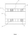
- the image sensor 10contains pixels 12, with filters responsive to NIR light only and pixels 14, 16 and 18 responsive to Red, Green and Blue light respectively.
- the image sensormay operate in multiple modes, as follows:
- the image sensormay read out an image comprised of only pixels with associated RGB images. Typically this will be a subset of the total active image sensor area, for example if the image sensor comprises a matrix of 2,048 ⁇ 2,048 pixels, a 512 ⁇ 512 subset of the pixels may be read out from the image sensor where 3 out of 4 pixels on each row are skipped and 3 out of 4 rows are skipped such that only those pixels with an associated R, G or B filter are read out.
- FIG. 2demonstrates how such images may be read out, where pixels that are read out are denoted by numerals 24, RGB pixels by numeral 26 and non-read out areas of the image sensor by numeral 28.
- a subset of the total image areasuch as a 512 ⁇ 512 image may be read out from the image sensor in binning and/or skipping mode, all Red, Green, and Blue sensitive pixels are skipped so that only NIR sensitive pixels are read out.
- a first imageis read out from the image sensor while the infrared light is activated, and then an identical second image is read out where the infrared light is not active. The second image is subtracted from the first image, resulting in a third image that comprises only infrared light-the so-called "Clean IR" image.
- the two imagesshould be captured very close in time to ensure minimal defects caused by objects having moved between the two images.
- the actively illuminated imagemay be captured before or after the non-lit image.
- ROIRegion of Interest mode
- a subset of the active area of an image sensoris read out so as to contain within the image certain features.
- eye trackingit is known to read out only a portion of a total image area containing an eye, or eyes, of a user. See for example, U.S. Pat. No. 7,572,008 for more information.
- a region of interestmay be read out using just NIR sensitive pixels or including all pixels (also Red, Green and Blue) within an area.
- NIR sensitive pixelsalso Red, Green and Blue
- the concept of a Clean IR imagecan be used also when capturing region of interest images. Even if some of the pixels are sensitive also to visible light, the image remaining after subtraction of an ambient light image will only be the image caused by the active illumination, which in case of a NIR illuminator will be a NIR image.
- a portion of the active area of an image sensoris read out while strobing NIR illumination from an illumination source. All pixels collect at least a portion of this strobed illumination, as well as ambient NIR illumination.
- the Red, Green and Blue pixelswill also collect a portion of ambient visible light. These Red, Green and Blue pixels will thus have higher values than if they were pure NIR pixels. In an eye tracking device, in the case of a short exposure time, these images may still be used to determine a glint from the pupil of a user.
- the Red, Green and Blue pixelsmay register high values while the NIR pixels register relatively low values. This is due to the sensor having lower quantum efficiency at the wavelength of the NIR illumination than at the wavelengths of visible light.
- pixel gain and pixel offsetcan be set differently for NIR and Red, Green, and Blue pixels. For instance the gain of Red, Green and Blue pixels may be set lower than that of the NIR pixels. If this is the case it must later on be compensated for in the algorithms.
- the imagesmay be captured as 10 or 12 bits of data per pixel, but then, especially in the mode of clean IR after having subtracted an ambient light image, the image may be transferred into 10, 8 or even fewer bits per pixel.
- a processing device connected to the image sensormay interpolate data read out from the sensor to replace the Red, Green and Blue pixel values with average NIR values from adjacent pixels.
- regions of interest read out of the image sensormay have varying characteristics.
- the region of interestmay be oriented horizontally or vertically. Further, more than one region of interest may be read out of the image sensor simultaneously.
- one region of interestmay be read out comprising both eyes of a user.
- This region of interestalso comprises extra information, such as the area of the persons face between the two eyes. This extra information is not needed for eye tracking, and thus the power and data use in capturing this extra information is wasted.
- By reading out two regions of interest comprising substantially a single eye or pupil eachexcess data and power is not consumed, and at the same time the read out time is minimized. If the sensor is of a rolling shutter type, this also means that the amount of ambient light being collected by the sensor is minimized.
- the image sensormay function in multiple orientations. For example, it is advantageous, due to the natural shape of an eye, to read out a substantially landscape view of a user's eye. In a normally oriented image sensor, this is possible due to the image sensor having typically a landscape layout of pixels (a larger size in the x-dimension than in the y-dimension), but if the image sensor is rotated (such as may be the case in portable device such as a phone or tablet), the image sensor cannot read out a landscape region of interest comprising only an eye. In order to capture the entire eye or pupil, the image sensor would have to read out a large portrait image.
- multiple regionsmay be read out forming a rectangle or square. These may be read out using a standard image transfer format such as the MIPI standard published by The MIPI Alliance (www.mipi.org).
- the read out interfacemay be a sensor internal interface that transfers image data to a second layer of the sensor containing processing capabilities.
- This kind of 3D stacked sensors containing an active photosensing layer stacked with a processing layer and often also a third memory/RAM layerhave become more and more common in the last year, specifically in smart phones.
- These four regions of interestmay be used to form any orientation of shape, for example they may be used to form a diagonally oriented shape.
- One specific implementation for multiple region of interests that is optimized for eye tracking purposesis to always have four non-overlapping equally sized regions of interest read out, for example each region may be 120x120 pixels in size.
- the sum of these regions of interestsare placed to include the expected positions of the two eyes of a person located in front of an eye tracker comprising an image sensor according to the present invention.
- the two top most regions of interestare always located on the same rows, the two bottom most are also located on the same rows, the two left most are located on the same columns and the two right most are located on the same columns.
- the two top most regions of interestare always located on the same rows, the two bottom most are also located on the same rows, the two left most are located on the same columns and the two right most are located on the same columns.
- the four regions of interestis then read out and combined into a single 240x240 image.
- an image of 240x241 pixelsmay be sent out from the sensor where the first or last line may include meta data describing the coordinates of the regions of interests on the sensor and other data of relevance for the algorithms to be able to use the image.
- the senormay enter a mode using 2x2 skipping yet still operating in the previously described mode in order to reduce all objects to half size in image pixels while still keeping the same read out format and approximately the same read out time.
- FIG. 6shows various possible orientations for multiple regions of interest.
- a user's eyesare displayed as circles, and regions of interest are shown as squares.
- FIG. 3allows for a low resolution image where it is often possible to determine a glint in an eye tracking system since the gaps between pixels that are read out are fairly small so no imaged objects can fall between read out pixels.
- FIG. 5shows an example of such a sequence.
- a first and second imageare read out in accordance with the Clean IR aspect of the invention previously described.
- a third imageis then read out from the image sensor according to the RGB aspect of the present invention previously described.
- Following this third imageare four Region of Interest (ROI) images according to the previously described aspect of the present invention.
- ROIRegion of Interest
- the fourth image in the sequenceis an ROI image having the DP effect, namely an illuminator off-axis from the image sensor has emitted infrared illumination towards the pupil of a user.
- the fifth and optional sixth images of the sequenceare ROI images having the BP effect, namely an illuminator on-axis with the image sensor has emitted infrared illumination towards the pupil of a user.
- the seventh and final image in the sequenceis an ROI image captured with the DP illuminator lit.
- the optional sixth image including only ambient lightmay be subtracted from the seventh and/or the fourth image in the sequence in order to subtract ambient light and isolate only active illumination in the DP images.
- the primary trade-off hereis that the images have been captured further apart in time and subtraction of one from the other has a higher risk of adding artefacts due to objects having moved between the exposures.
- this sequence of imagesis approximate to the fourth, fifth, sixth and seventh images in the previously described sequence of images.
- a full image sequencei.e., a burst mode
- a full image sequencei.e., a burst mode
- only the ROI size/position of the overall available imagemay be updated for subsequent images while in burst mode.
- the senorgo into a low power mode directly after the image sequence has been captured. In this low power mode the sensor should preferably still be responsive to reprogramming of the next image sequence while most of the other parts of the sensor are asleep.
- an image sensoris therefore adapted to allow for three forms of images: RGB, subsampled images through binning or skipping, and ROI or cropped images.
- RGBRGB
- subsampled images through binning or skippingROI or cropped images.
- ROI or cropped imagesFor the latter two types of images, two subsequent image captures, one with active illumination and one without, may be used to create a Clean IR version of the image.
- This image sensortherefore may function in a variety of modes suitable for use in vision based human computer interaction.
- an RGB imagemay be used for facial identification, imaging such as Skype, regular image capture and the like, anti-spoofing when combined with NIR image based biometrics such as face or iris, or for determining eye position to guide Region of Interest readout, a subsampled image (Clean IR image or just a single illuminated image) may be used for facial recognition, facial feature tracking, or for determining eye position to guide Region of Interest readout, and Region of Interest images may be used for eye tracking.
- Another possible burst sequence which may be employed by image sensors described hereinmay include a sequence useful for low-power draw eye tracking and recognition of facial features, and is discussed with reference to FIG. 8 .
- three to five framesmay include data received for one imaging cycle.
- An optional first framemay include a binned or skipped NIR image (2x2 skipped and 2x2 binned shown).
- a second framemay also include a binned or skipped NIR image during a period of illumination by a NIR illuminator (2x2 skipped and 2x2 binned shown).
- a third frame in a region of interestmay include a combined NIR and RGB image during a period of illumination by a NIR illuminator.
- An optional fourth frame in a region of interestmay include a combined NIR and RGB image.
- a fifth frame in a region of interestmay include a combined NIR and RGB image during a period of illumination by a NIR illuminator.
- the second and third frames describedmay be employed in BP eye tracking, while the second and fifth frames may be employed for DP eye tracking.
- the image sensor employed in this or other sequencesmay be a NIR-only sensor, without visible light or RGB pixels. This may be a useful solution for eye tracking, facial feature tracking, and/or machine vision with active NIR illumination. While such a sensor cannot output RGB images, it can perform the NIR functions detailed herein.
- a burst sequence which may be employed by image sensors described hereinmay include a sequence useful for low-power draw eye tracking, and is discussed with reference to FIG. 9 .
- two to three framesmay include data received for one imaging cycle.
- a first frame in a region of interestmay include a combined NIR and RGB image during a period of illumination by a NIR illuminator.
- An optional second frame in a region of interestmay include a combined NIR and RGB image.
- a third frame in a region of interestmay include a combined NIR and RGB image during a period of illumination by a NIR illuminator.
- the first frame describedmay be employed in BP eye tracking, while the third frame may be employed for DP eye tracking.
- the image sensor employed in this or other sequencesmay be a NIR-only sensor, without visible light or RGB pixels. This may be a useful solution for eye tracking, facial feature tracking, and/or machine vision with active NIR illumination. While such a sensor cannot output RGB images, it can perform the NIR functions detailed herein.
- a burst which may be employed by image sensors described hereinmay include a sequence useful for low-power draw eye tracking and recognition of facial features, and is discussed with reference to FIG. 10 .
- three framesmay include data received for one imaging cycle.
- a first framemay include a binned or skipped NIR image during a period of illumination by a NIR illuminator (2x2 skipped and 2x2 binned shown).
- a second frame in a region of interestmay include a combined NIR and RGB image during a period of illumination by a NIR illuminator.
- a third frame in a region of interestmay also include a combined NIR and RGB image during a period of illumination by a NIR illuminator.
- the first and second frames describedmay be employed in BP eye tracking, while the third frame may be employed for DP eye tracking.
- the image sensor employed in this or other sequencesmay be a NIR-only sensor, without visible light or RGB pixels. This may be a useful solution for eye tracking, facial feature tracking, and/or machine vision with active NIR illumination. While such a sensor cannot output RGB images, it can perform the NIR functions detailed herein.
- a burst which may be employed by image sensors described hereinmay include a sequence useful for low-power draw eye tracking, and is discussed with reference to FIG. 11 .
- two framesmay include data received for one imaging cycle.
- a first framemay include in a region of interest may include a combined NIR and RGB image during a period of illumination by a NIR illuminator.
- a second frame in a region of interestmay also include a combined NIR and RGB image during a period of illumination by a NIR illuminator.
- the first frame describedmay be employed in BP eye tracking, while the second frame may be employed for DP eye tracking.
- the image sensor employed in this or other sequencesmay be a NIR-only sensor, without visible light or RGB pixels. This may be a useful solution for eye tracking, facial feature tracking, and/or machine vision with active NIR illumination. While such a sensor cannot output RGB images, it can perform the NIR functions detailed herein.
- imaging sequencesusing either a combined RGB/NIR sensor, as described herein, or a NIR-only sensor as also described herein, may be possible within the scope of the invention.
- imaging sequencesmay include sequences disclosed in U.S. Patent Publication No. 2015/0262010 .
- the image sensors described hereinmay be useful for determining the presence of a user using low power Clean IR imaging sequences as described herein.
- a computing devicemay be in a sleep mode, and only a relevant imaging sensor may be operational to determine when the computing device should be woken.
- the sensormay be set to operate in an extreme sub sampling mode to achieve very low resolution, where preferable a large number of pixels are binned together to increase the sensor's signal to noise.
- some skippingis used to capture a frame during a period of illumination by a NIR illuminator followed closely in time by a frame from the same pixels without the NIR illumination. In this manner a Clean IR image is produced from the image sensor as described herein.
- different Clean IR images of very low resolutionmay be produced during various states of user presence (or non-presence) in front of the image sensor. By binning a large number of pixels, these images may be achieved with acceptable signal to noise at extremely short exposure times. In addition, these images may be achieved with low power consumption from illumination and also short time between the lit and the unlit image used to create the Clean IR image, thus minimizing motion or other temporal artefacts.
- the maximum pixel valueis less than a first value
- the average pixel valueis greater than a second value but less than a third value
- the quotient of the maximum pixel value divided by the average pixel valueis greater than a fourth value but less than a fifth value
- the quotient of the average pixel value divided by the average pixel value of the previous image to the current imageis greater than a sixth value but less than a seventh value
- the first through sixth valueare predetermined or dynamic and set to facilitate these variables being useful for detecting user presence.
- the processis repeated and at a certain threshold total number of potential detections, a user determined to be likely present and the computing device is awoken by a processor so instructed. If any of the above comparisons are false however, the entire process repeats by resetting the number of potential detections to zero and beginning analysis of images per the above anew.
- any kind of machine vision algorithmcan be used to detect presence.
- using a Clean IR imageonly what is illuminated by the active NIR illuminator of the system is detected. A person sitting closer to the illuminator may appear brighter and larger, and a person sitting farther away may appear smaller and less bright.
- the illuminatormay also be covered and the sensor will capture a pure white image. If a human head and upper body is to be captured within a predefined distance from the sensor (e.g., 20-70 cm from the sensor), it is possible to set one or more thresholds indicating the size and brightness of the object being captured. For example, a threshold indicating a first size or brightness may indicate someone or something closer than 20 cm from the sensor (e.g., the captured object is too large and/or too bright). Similarly, another threshold indicating a second size or brightness may indicate someone or something farther from 70 cm from the sensor (e.g., the object is too small and/or too dark to trigger the system). Although 20 cm and 70 cm are provided as examples, other distances or criteria may be used.
- FIG. 7is a block diagram illustrating an exemplary computer system 700 in which embodiments of the present invention may be implemented.
- This exampleillustrates a computer system 700 such as may be used, in whole, in part, or with various modifications, to provide the functions of the components of the invention such as those discussed above.
- any of the functions discussed above of the image sensormay be controlled by the computer system 700.
- the computer system 700is shown comprising hardware elements that may be electrically coupled via a bus 790.
- the hardware elementsmay include one or more central processing units 710, one or more input devices 720 (e.g., a mouse, a keyboard, etc.), and one or more output devices 730 (e.g., a display device, a printer, etc.).
- the computer system 700may also include one or more storage device 740.
- storage device(s) 740may be disk drives, optical storage devices, solid-state storage device such as a random access memory (“RAM”) and/or a read-only memory (“ROM”), which can be programmable, flash-updateable and/or the like.
- RAMrandom access memory
- ROMread-only memory
- the computer system 700may additionally include a computer-readable storage media reader 750, a communications system 760 (e.g., a modem, a network card (wireless or wired), an infra-red communication device, BluetoothTM device, cellular communication device, etc.), and working memory 780, which may include RAM and ROM devices as described above.
- the computer system 700may also include a processing acceleration unit 770, which can include a digital signal processor, a special-purpose processor and/or the like.
- the computer-readable storage media reader 750can further be connected to a computer-readable storage medium, together (and, optionally, in combination with storage device(s) 740) comprehensively representing remote, local, fixed, and/or removable storage devices plus storage media for temporarily and/or more permanently containing computer-readable information.
- the communications system 760may permit data to be exchanged with a network, system, computer and/or other component described above.
- the computer system 700may also comprise software elements, shown as being currently located within a working memory 780, including an operating system 784 and/or other code 788. It should be appreciated that alternate embodiments of a computer system 700 may have numerous variations from that described above. For example, customized hardware might also be used and/or particular elements might be implemented in hardware, software (including portable software, such as applets), or both. Furthermore, connection to other computing devices such as network input/output and data acquisition devices may also occur.
- Software of computer system 700may include code 788 for implementing any or all of the function of the various elements of the architecture as described herein.
- softwarestored on and/or executed by a computer system such as system 700, can provide the functions of components discussed herein, and/or other components of the invention such as those discussed above. Methods implementable by software on some of these components have been discussed above in more detail.
Landscapes
- Engineering & Computer Science (AREA)
- Multimedia (AREA)
- Signal Processing (AREA)
- Physics & Mathematics (AREA)
- Spectroscopy & Molecular Physics (AREA)
- Health & Medical Sciences (AREA)
- General Health & Medical Sciences (AREA)
- Ophthalmology & Optometry (AREA)
- Human Computer Interaction (AREA)
- General Physics & Mathematics (AREA)
- Theoretical Computer Science (AREA)
- Computer Vision & Pattern Recognition (AREA)
- Image Processing (AREA)
- Studio Devices (AREA)
Description
- In one embodiment, an image sensor according to
claim 1 is provided. - In another embodiment, a method for capturing images according to
claim 12 is provided. - A non-transitory machine readable medium having instructions stored thereon for capturing images shall be described. The instructions may be executable by one or more processors to process signals produced by a first portion of a plurality of pixels receiving light. Receiving light at the first portion of the plurality of pixels may include blocking red, green, and blue light at each pixel of the first portion of the plurality of pixels with a near-infrared filter. Receiving light at the first portion of the plurality of pixels may also include receiving near-infrared light at each pixel of the first portion of the plurality of pixels. The instructions may also be executable to process signals produced by a second portion of the plurality of pixels receiving light. Receiving light at the second portion of the plurality of pixels may include receiving one of red, green, or blue light at each pixel of the second portion of the plurality of pixels. Receiving light at the second portion of the plurality of pixels may also include receiving near-infrared light at each pixel of the second portion of the plurality of pixels.
- The present invention is described in conjunction with the appended figures:
FIG. 1 is a diagram view of one image sensor of the invention;FIG. 2 is a diagram view of the image sensor ofFIG. 1 where only two rows are being activated;FIG. 3 is a diagram view of another image sensor of the invention where binning is employed;FIG. 4 is a diagram view of the image sensor ofFIG. 1 where skipping is employed;FIG. 5 is a diagram view of a sequence of images obtained in a single cycle of a bust mode imaging process;FIG. 6 is a diagram view of various configurations of multiple areas of interest imaged by image sensors of the invention;FIG. 7 is a block diagram of an exemplary computer system capable of being used in at least some portion of the apparatuses or systems of the present invention, or implementing at least some portion of the methods of the present invention;FIG. 8 is a diagram view of a sequence of images obtained in a single cycle of another bust mode imaging process;FIG. 9 is a diagram view of a sequence of images obtained in a single cycle of another bust mode imaging process;FIG. 10 is a diagram view of a sequence of images obtained in a single cycle of another bust mode imaging process;FIG. 11 is a diagram view of a sequence of images obtained in a single cycle of another bust mode imaging process; andFIG. 12 is a diagram view of different Clean IR images potentially registering the presence or absence of a user in view of image sensors of the invention.- In the appended figures, similar components and/or features may have the same numerical reference label. Further, various components of the same type may be distinguished by following the reference label by a letter that distinguishes among the similar components and/or features. If only the first numerical reference label is used in the specification, the description is applicable to any one of the similar components and/or features having the same first numerical reference label irrespective of the letter suffix.
- The present invention generally relates to an image sensor particularly suited for vision based human computer interaction, and methods for using said image sensor.
- Image sensors of different types, functions, and designs are well known. Typically an image sensor is adapted to function in a wide variety of fields.
- Fundamentally an image sensor is comprised of a photosensitive substrate containing multiple photosites, when light photons are collected in a photosite - an electrical charge is produced. Typically one photosite is associated with one pixel of an image sensor. The size of the electrical charge is dependent on the amount of light collected, such that a brighter light will result in a higher charge. Once an exposure is complete, each photosites electrical charge is measured and turned into a digital value by an analogue-to-digital converter.
- Two forms of image sensor technology comprise the majority of today's image sensors-CCD and CMOS image sensors. A Charge-Coupled Device (CCD) image sensor comprises multiple pixels represented by p-doped MOS capacitors. These capacitors allow for conversion of incoming photons into electron charges at the semiconductor-oxide interface, the CCD then reads out these charges via a gate structure that requires a separate power source.
- The most common form of image sensor today is a CMOS image sensor, where the image sensor is an active pixel sensor made using Complementary Metal-Oxide-Semiconductor (CMOS) technology. Fundamentally the CMOS image sensor operates in the same way as a CCD image sensor, however it is manufactured using a much higher yield process. A CMOS image sensor contains a large array of transistors comprising a photodiode and amplifier. The photodiodes accumulate electrical charge when exposed to light, and those charges are then converted to voltage, amplified and transmitted as electrical signals.
- CMOS image sensors typically consume less power than a CCD image sensor and can read out electrical charges much more rapidly.
- As an image sensor fundamentally only records the level of light, in order to record color information a Bayer filter is typically used. A Bayer filter is a color filter bonded to the sensor substrate which allows only photons of a certain color to enter each pixel. By alternating the filter across the pixels between red, green and blue, light of different colors can be recorded by different adjacent pixels.
- Although previous image sensors have been proposed for functioning with vision based human computer interaction, an image sensor using the techniques herein described has not been previously described, particularly for use in eye tracking technology.
WO2016/018586A1 describes an imaging sensor for low light level color imaging includes an array of pixels. Each pixel has a first pixel portion that has a first photosensitive area and is responsive to light in a panchromatic spectral range and a second pixel portion that has a second photosensitive area and is responsive to light in a sub-band spectral range. The first photosensitive area is greater than the second photosensitive area and the sub-band spectral range is narrower than and contained within the panchromatic spectral range. The first and second pixel portions of each pixel are independently addressable.US2015/373278A1 describes an image processing apparatus including an image acquirement section, a correction section, and an image production section. The image acquirement section acquires an image signal representing an image, the image signal is generated by light receiving elements that receive lights from a specific space preliminarily defined in a vicinity of a vehicle via a near infrared passing filter mainly transmitting near infrared lights and a visible light passing filter transmitting visible lights and near infrared lights, respectively. The image includes multiple areas and indicates the specific space projected onto a plane. The correction section corrects each area of the image by amplifying intensity of near infrared lights with an increasing amplification factor when a difference between the intensity of near infrared lights and intensity of visible lights and near infrared lights becomes smaller. The image production section produces a new image based on the corrected areas of the image.- In
US7012643B2 , a high sensitivity, single chip, low light level imaging device is provided. The imaging device utilizes sparse color sampling, to maximize the luminance information gathered. In particular, color information is gathered by a small proportion of the pixels included in an image sensor, while the remaining pixels operate at full spectrum sensitivity. - It is an object of the present invention to propose an image sensor adapted to function with eye tracking, and other vision based human computer interaction technology.
- The ensuing description provides exemplary embodiments only, and is not intended to limit the scope, applicability or configuration of the disclosure. Rather, the ensuing description of the exemplary embodiments will provide those skilled in the art with an enabling description for implementing one or more exemplary embodiments. It being understood that various changes may be made in the function and arrangement of elements without departing from the scope of the claims.
- To begin then, an object of the present invention is to provide an image sensor suitable for use with vision based human computer interaction. According to a first aspect of the present invention, there is provided an image sensor containing an integrated Bayer filter and near-infrared light (NIR) filter.
- As would be readily understood by a person of skill in the art, a Bayer filter filters visible light apart from Red, Green or Blue (RGB) light from entering a pixel, or pixels, of an image sensor. An NIR filter typically prevents light below approximately 650 nanometers (nm) from entering a pixel, or pixels, of an image sensor. NIR light may be light at 850 nm, 905 nm, 940 nm, 1100 nm, and/or some other NIR wavelength.
- As many vision based human computer interaction technologies, such as eye tracking, require infrared light to function, it is advantageous that an image sensor be adapted to incorporate both forms of filter.
- Eye tracking is one example of a vision based human computer interaction technology. In eye tracking, at least one image sensor and at least one illuminator combine to determine the direction of a user's gaze. There are generally two types of eye tracking techniques: "Bright Pupil" (BP) and "Dark Pupil" (DP). BP eye tracking comprises an illumination source coaxial with the optical path of an image sensor, a user's eye then acts as a retroreflector as the light from the illumination source reflects off the retina, creating a bright pupil effect similar to red eye. If the illumination source is non-coaxial, as in DP eye tracking, then the pupil appears dark because the retroreflection from the retina is directed away from the camera.
- Both eye tracking techniques function adequately, most often using Near Infrared Illumination. BP eye tracking creates greater iris/pupil contrast, but is more sensitive to ambient light such as is present outdoors. While DP eye tracking generally functions with more ethnicities than BP eye tracking. The present invention can function with either form of eye tracking.
- In order to achieve an image sensor that filters both RGB and NIR light, several alternatives exist. Each will be described here in the context of the present invention.
- In the first alternative, a sensor is provided with dimensions for example of 2,048 pixels x 2,048 pixels. 15 out of 16 pixels have a filter associated therewith which allows only NIR light to enter, while 1 pixel out of 16 allows only Red, Green or Blue light as well as NIR light to enter. In some embodiments, the red, green, and blue pixels may include an NIR filter, and not allow NIR light to pass. In yet other embodiments, red, green, and blue pixels will not be present, possibly especially in embodiments where only eye tracking and not facial feature detection is necessary. In any embodiment discussed herein, different pixel layouts and resolutions may be employed than what is discussed or shown, as the specific embodiments disclosed are merely example configurations of the constructs disclosed.
- This allows the image sensor to function as both a traditional RGB image sensor, as well as a NIR sensitive image sensor.
- With reference to
FIG. 1 , a portion of animage sensor 10 is shown in simplified form for illustrative purposes. Theimage sensor 10 containspixels 12, with filters responsive to NIR light only andpixels - In use, the image sensor may operate in multiple modes, as follows:
- In RGB mode the image sensor may read out an image comprised of only pixels with associated RGB images. Typically this will be a subset of the total active image sensor area, for example if the image sensor comprises a matrix of 2,048×2,048 pixels, a 512×512 subset of the pixels may be read out from the image sensor where 3 out of 4 pixels on each row are skipped and 3 out of 4 rows are skipped such that only those pixels with an associated R, G or B filter are read out.
FIG. 2 demonstrates how such images may be read out, where pixels that are read out are denoted bynumerals 24, RGB pixels bynumeral 26 and non-read out areas of the image sensor bynumeral 28. - When reading out the image, only sensor lines having Red, Green, or Blue pixels are read out. The read-out data is run through a 1×3 kernel to subtract the average values of the adjacent NIR pixels from the Red, Green and Blue pixels respectively such that their values represent only the signal from the intended color. Subsequent to this only data from the quarter of the remaining pixels that represent the Red, Green, and Blue pixels that have been NIR compensated are kept. Data from the remaining three quarters of pixels are discarded.
- A subset of the total image area, such as a 512×512 image may be read out from the image sensor in binning and/or skipping mode, all Red, Green, and Blue sensitive pixels are skipped so that only NIR sensitive pixels are read out. A first image is read out from the image sensor while the infrared light is activated, and then an identical second image is read out where the infrared light is not active. The second image is subtracted from the first image, resulting in a third image that comprises only infrared light-the so-called "Clean IR" image.
- Ideally the two images should be captured very close in time to ensure minimal defects caused by objects having moved between the two images. The actively illuminated image may be captured before or after the non-lit image.
- In a Region of Interest mode (ROI), a subset of the active area of an image sensor is read out so as to contain within the image certain features. For example, in eye tracking it is known to read out only a portion of a total image area containing an eye, or eyes, of a user. See for example,
U.S. Pat. No. 7,572,008 for more information. - In the present invention, a region of interest may be read out using just NIR sensitive pixels or including all pixels (also Red, Green and Blue) within an area. The concept of a Clean IR image can be used also when capturing region of interest images. Even if some of the pixels are sensitive also to visible light, the image remaining after subtraction of an ambient light image will only be the image caused by the active illumination, which in case of a NIR illuminator will be a NIR image.
- A portion of the active area of an image sensor is read out while strobing NIR illumination from an illumination source. All pixels collect at least a portion of this strobed illumination, as well as ambient NIR illumination. The Red, Green and Blue pixels will also collect a portion of ambient visible light. These Red, Green and Blue pixels will thus have higher values than if they were pure NIR pixels. In an eye tracking device, in the case of a short exposure time, these images may still be used to determine a glint from the pupil of a user.
- In this mode, the Red, Green and Blue pixels may register high values while the NIR pixels register relatively low values. This is due to the sensor having lower quantum efficiency at the wavelength of the NIR illumination than at the wavelengths of visible light. To minimize the impact of this issue and to better utilize the pixel dynamics, pixel gain and pixel offset can be set differently for NIR and Red, Green, and Blue pixels. For instance the gain of Red, Green and Blue pixels may be set lower than that of the NIR pixels. If this is the case it must later on be compensated for in the algorithms.
- Alternatively, or additionally, the images may be captured as 10 or 12 bits of data per pixel, but then, especially in the mode of clean IR after having subtracted an ambient light image, the image may be transferred into 10, 8 or even fewer bits per pixel.
- As an optional improvement, a processing device connected to the image sensor may interpolate data read out from the sensor to replace the Red, Green and Blue pixel values with average NIR values from adjacent pixels.
- Further, in another aspect of the present invention, regions of interest read out of the image sensor may have varying characteristics. For example, the region of interest may be oriented horizontally or vertically. Further, more than one region of interest may be read out of the image sensor simultaneously.
- Consider the example use case of eye tracking, in traditional imaging technology, one region of interest may be read out comprising both eyes of a user. This region of interest also comprises extra information, such as the area of the persons face between the two eyes. This extra information is not needed for eye tracking, and thus the power and data use in capturing this extra information is wasted. By reading out two regions of interest comprising substantially a single eye or pupil each, excess data and power is not consumed, and at the same time the read out time is minimized. If the sensor is of a rolling shutter type, this also means that the amount of ambient light being collected by the sensor is minimized.
- By reading out regions of interest with varying orientations, the image sensor may function in multiple orientations. For example, it is advantageous, due to the natural shape of an eye, to read out a substantially landscape view of a user's eye. In a normally oriented image sensor, this is possible due to the image sensor having typically a landscape layout of pixels (a larger size in the x-dimension than in the y-dimension), but if the image sensor is rotated (such as may be the case in portable device such as a phone or tablet), the image sensor cannot read out a landscape region of interest comprising only an eye. In order to capture the entire eye or pupil, the image sensor would have to read out a large portrait image.
- In order to affect a rectangular or square image readout, multiple regions, such as four, may be read out forming a rectangle or square. These may be read out using a standard image transfer format such as the MIPI standard published by The MIPI Alliance (www.mipi.org). Alternatively the read out interface may be a sensor internal interface that transfers image data to a second layer of the sensor containing processing capabilities. This kind of 3D stacked sensors containing an active photosensing layer stacked with a processing layer and often also a third memory/RAM layer have become more and more common in the last year, specifically in smart phones. These four regions of interest may be used to form any orientation of shape, for example they may be used to form a diagonally oriented shape.
- Further, it is known that power consumption scales at an approximate rate to the increase in read out area. By not reading out the area between the eyes, pixels and analog-to-digital converters (ADCs) can be powered down for those areas. An image sensor according to the current state of the art reads out complete rows, which provides unnecessary power for pixels not of interest.
- One specific implementation for multiple region of interests that is optimized for eye tracking purposes is to always have four non-overlapping equally sized regions of interest read out, for example each region may be 120x120 pixels in size. The sum of these regions of interests are placed to include the expected positions of the two eyes of a person located in front of an eye tracker comprising an image sensor according to the present invention.
- Further, there is also an additional restriction that the two top most regions of interest are always located on the same rows, the two bottom most are also located on the same rows, the two left most are located on the same columns and the two right most are located on the same columns. Thus, for a given size of the regions of interest only two 'x' coordinates and two 'y' coordinates are needed to fully define the regions to read out.
- The four regions of interest, each being 120x120 pixels, is then read out and combined into a single 240x240 image. Alternatively an image of 240x241 pixels may be sent out from the sensor where the first or last line may include meta data describing the coordinates of the regions of interests on the sensor and other data of relevance for the algorithms to be able to use the image.
- The benefit of this approach is that the read out time for a multiple regions of interest image will be the same independent of the head orientation of a user and read out area is minimized to lower the negative impact of ambient light on the performance of the eye tracker.
- Additionally, if a user is leaning forward towards an eye tracker and due to their proximity to the eye tracker, the eyes of the person, too large to fit within a 120x120 region of interest, the sensor may enter a mode using 2x2 skipping yet still operating in the previously described mode in order to reduce all objects to half size in image pixels while still keeping the same read out format and approximately the same read out time.
- In order to illustrate this aspect of the present invention,
FIG. 6 shows various possible orientations for multiple regions of interest. InFIG. 6 , a user's eyes are displayed as circles, and regions of interest are shown as squares. - According to the present invention, two different forms of binning and/or skipping may be used. These are demonstrated in
FIG. 3 andFIG. 4 .FIG. 3 allows for a low resolution image where it is often possible to determine a glint in an eye tracking system since the gaps between pixels that are read out are fairly small so no imaged objects can fall between read out pixels. - According to the present invention, it is possible to operate the image sensor in a burst sequence of several modes.
FIG. 5 shows an example of such a sequence. - In this example sequence, which may be performed in any order, a first and second image are read out in accordance with the Clean IR aspect of the invention previously described. A third image is then read out from the image sensor according to the RGB aspect of the present invention previously described. Following this third image are four Region of Interest (ROI) images according to the previously described aspect of the present invention.
- These four ROI images will now be described in greater detail in the context of their use in an eye tracking system. In an eye tracking system it is desirable to generate images which illustrate a "dark pupil" effect and images which illustrate a "bright pupil" effect. These effects and their use in eye tracking have been previously described in this specification, and would be readily understood by a person of skill in the art.
- The fourth image in the sequence is an ROI image having the DP effect, namely an illuminator off-axis from the image sensor has emitted infrared illumination towards the pupil of a user. The fifth and optional sixth images of the sequence are ROI images having the BP effect, namely an illuminator on-axis with the image sensor has emitted infrared illumination towards the pupil of a user. The seventh and final image in the sequence is an ROI image captured with the DP illuminator lit. Optionally, the optional sixth image including only ambient light may be subtracted from the seventh and/or the fourth image in the sequence in order to subtract ambient light and isolate only active illumination in the DP images. The primary trade-off here is that the images have been captured further apart in time and subtraction of one from the other has a higher risk of adding artefacts due to objects having moved between the exposures.
- In a further aspect of the present invention, it is possible to read out a sequence of images only comprising images suitable for eye tracking. In this aspect of the present invention, this sequence of images is approximate to the fourth, fifth, sixth and seventh images in the previously described sequence of images.
- It is preferable to have a sensor where a full image sequence (i.e., a burst mode) can be programmed at once, including illumination type and timing, exposure times, gain, binning/skipping, ROI size and position, etc. for each image. In some embodiments, only the ROI size/position of the overall available image may be updated for subsequent images while in burst mode.
- It is also preferable to have the sensor go into a low power mode directly after the image sequence has been captured. In this low power mode the sensor should preferably still be responsive to reprogramming of the next image sequence while most of the other parts of the sensor are asleep.
- As described herein, an image sensor is therefore adapted to allow for three forms of images: RGB, subsampled images through binning or skipping, and ROI or cropped images. For the latter two types of images, two subsequent image captures, one with active illumination and one without, may be used to create a Clean IR version of the image. This image sensor therefore may function in a variety of modes suitable for use in vision based human computer interaction. For example, an RGB image may be used for facial identification, imaging such as Skype, regular image capture and the like, anti-spoofing when combined with NIR image based biometrics such as face or iris, or for determining eye position to guide Region of Interest readout, a subsampled image (Clean IR image or just a single illuminated image) may be used for facial recognition, facial feature tracking, or for determining eye position to guide Region of Interest readout, and Region of Interest images may be used for eye tracking.
- Another possible burst sequence which may be employed by image sensors described herein may include a sequence useful for low-power draw eye tracking and recognition of facial features, and is discussed with reference to
FIG. 8 . In this burst sequence, three to five frames may include data received for one imaging cycle. An optional first frame may include a binned or skipped NIR image (2x2 skipped and 2x2 binned shown). A second frame may also include a binned or skipped NIR image during a period of illumination by a NIR illuminator (2x2 skipped and 2x2 binned shown). A third frame in a region of interest may include a combined NIR and RGB image during a period of illumination by a NIR illuminator. An optional fourth frame in a region of interest may include a combined NIR and RGB image. A fifth frame in a region of interest may include a combined NIR and RGB image during a period of illumination by a NIR illuminator. The second and third frames described may be employed in BP eye tracking, while the second and fifth frames may be employed for DP eye tracking. In some embodiments, the image sensor employed in this or other sequences may be a NIR-only sensor, without visible light or RGB pixels. This may be a useful solution for eye tracking, facial feature tracking, and/or machine vision with active NIR illumination. While such a sensor cannot output RGB images, it can perform the NIR functions detailed herein. - Another possible burst sequence which may be employed by image sensors described herein may include a sequence useful for low-power draw eye tracking, and is discussed with reference to
FIG. 9 . In this burst sequence, two to three frames may include data received for one imaging cycle. A first frame in a region of interest may include a combined NIR and RGB image during a period of illumination by a NIR illuminator. An optional second frame in a region of interest may include a combined NIR and RGB image. A third frame in a region of interest may include a combined NIR and RGB image during a period of illumination by a NIR illuminator. The first frame described may be employed in BP eye tracking, while the third frame may be employed for DP eye tracking. In some embodiments, the image sensor employed in this or other sequences may be a NIR-only sensor, without visible light or RGB pixels. This may be a useful solution for eye tracking, facial feature tracking, and/or machine vision with active NIR illumination. While such a sensor cannot output RGB images, it can perform the NIR functions detailed herein. - Another possible burst which may be employed by image sensors described herein may include a sequence useful for low-power draw eye tracking and recognition of facial features, and is discussed with reference to
FIG. 10 . In this burst sequence, three frames may include data received for one imaging cycle. A first frame may include a binned or skipped NIR image during a period of illumination by a NIR illuminator (2x2 skipped and 2x2 binned shown). A second frame in a region of interest may include a combined NIR and RGB image during a period of illumination by a NIR illuminator. A third frame in a region of interest may also include a combined NIR and RGB image during a period of illumination by a NIR illuminator. The first and second frames described may be employed in BP eye tracking, while the third frame may be employed for DP eye tracking. In some embodiments, the image sensor employed in this or other sequences may be a NIR-only sensor, without visible light or RGB pixels. This may be a useful solution for eye tracking, facial feature tracking, and/or machine vision with active NIR illumination. While such a sensor cannot output RGB images, it can perform the NIR functions detailed herein. - Another possible burst which may be employed by image sensors described herein may include a sequence useful for low-power draw eye tracking, and is discussed with reference to
FIG. 11 . In this burst sequence, two frames may include data received for one imaging cycle. A first frame may include in a region of interest may include a combined NIR and RGB image during a period of illumination by a NIR illuminator. A second frame in a region of interest may also include a combined NIR and RGB image during a period of illumination by a NIR illuminator. The first frame described may be employed in BP eye tracking, while the second frame may be employed for DP eye tracking. In some embodiments, the image sensor employed in this or other sequences may be a NIR-only sensor, without visible light or RGB pixels. This may be a useful solution for eye tracking, facial feature tracking, and/or machine vision with active NIR illumination. While such a sensor cannot output RGB images, it can perform the NIR functions detailed herein. - Other possible imaging sequences, using either a combined RGB/NIR sensor, as described herein, or a NIR-only sensor as also described herein, may be possible within the scope of the invention. Merely by way of example, such imaging sequences may include sequences disclosed in
U.S. Patent Publication No. 2015/0262010 . - In another embodiment, the image sensors described herein may be useful for determining the presence of a user using low power Clean IR imaging sequences as described herein. A computing device may be in a sleep mode, and only a relevant imaging sensor may be operational to determine when the computing device should be woken. In some of these embodiments, the sensor may be set to operate in an extreme sub sampling mode to achieve very low resolution, where preferable a large number of pixels are binned together to increase the sensor's signal to noise. In some cases, some skipping is used to capture a frame during a period of illumination by a NIR illuminator followed closely in time by a frame from the same pixels without the NIR illumination. In this manner a Clean IR image is produced from the image sensor as described herein. As shown in
FIG. 12 , different Clean IR images of very low resolution may be produced during various states of user presence (or non-presence) in front of the image sensor. By binning a large number of pixels, these images may be achieved with acceptable signal to noise at extremely short exposure times. In addition, these images may be achieved with low power consumption from illumination and also short time between the lit and the unlit image used to create the Clean IR image, thus minimizing motion or other temporal artefacts. - From the Clean IR images receiving in this process, two parameters may be extracted: the maximum pixel value, and the average pixel value. In one embodiment, if (A) the maximum pixel value is less than a first value, (B) the average pixel value is greater than a second value but less than a third value, (C) the quotient of the maximum pixel value divided by the average pixel value is greater than a fourth value but less than a fifth value, and (D) the quotient of the average pixel value divided by the average pixel value of the previous image to the current image is greater than a sixth value but less than a seventh value, then the presence of a user is potentially detected. The first through sixth value are predetermined or dynamic and set to facilitate these variables being useful for detecting user presence. The process is repeated and at a certain threshold total number of potential detections, a user determined to be likely present and the computing device is awoken by a processor so instructed. If any of the above comparisons are false however, the entire process repeats by resetting the number of potential detections to zero and beginning analysis of images per the above anew. In general, any kind of machine vision algorithm can be used to detect presence. In some embodiments using a Clean IR image, only what is illuminated by the active NIR illuminator of the system is detected. A person sitting closer to the illuminator may appear brighter and larger, and a person sitting farther away may appear smaller and less bright. If the person is too close or almost covering the lens in front of the sensor, the illuminator may also be covered and the sensor will capture a pure white image. If a human head and upper body is to be captured within a predefined distance from the sensor (e.g., 20-70 cm from the sensor), it is possible to set one or more thresholds indicating the size and brightness of the object being captured. For example, a threshold indicating a first size or brightness may indicate someone or something closer than 20 cm from the sensor (e.g., the captured object is too large and/or too bright). Similarly, another threshold indicating a second size or brightness may indicate someone or something farther from 70 cm from the sensor (e.g., the object is too small and/or too dark to trigger the system). Although 20 cm and 70 cm are provided as examples, other distances or criteria may be used.
FIG. 7 is a block diagram illustrating anexemplary computer system 700 in which embodiments of the present invention may be implemented. This example illustrates acomputer system 700 such as may be used, in whole, in part, or with various modifications, to provide the functions of the components of the invention such as those discussed above. For example, any of the functions discussed above of the image sensor may be controlled by thecomputer system 700.- The
computer system 700 is shown comprising hardware elements that may be electrically coupled via a bus 790. The hardware elements may include one or morecentral processing units 710, one or more input devices 720 (e.g., a mouse, a keyboard, etc.), and one or more output devices 730 (e.g., a display device, a printer, etc.). Thecomputer system 700 may also include one ormore storage device 740. By way of example, storage device(s) 740 may be disk drives, optical storage devices, solid-state storage device such as a random access memory ("RAM") and/or a read-only memory ("ROM"), which can be programmable, flash-updateable and/or the like. - The
computer system 700 may additionally include a computer-readablestorage media reader 750, a communications system 760 (e.g., a modem, a network card (wireless or wired), an infra-red communication device, Bluetooth™ device, cellular communication device, etc.), and workingmemory 780, which may include RAM and ROM devices as described above. In some embodiments, thecomputer system 700 may also include aprocessing acceleration unit 770, which can include a digital signal processor, a special-purpose processor and/or the like. - The computer-readable
storage media reader 750 can further be connected to a computer-readable storage medium, together (and, optionally, in combination with storage device(s) 740) comprehensively representing remote, local, fixed, and/or removable storage devices plus storage media for temporarily and/or more permanently containing computer-readable information. Thecommunications system 760 may permit data to be exchanged with a network, system, computer and/or other component described above. - The
computer system 700 may also comprise software elements, shown as being currently located within a workingmemory 780, including an operating system 784 and/orother code 788. It should be appreciated that alternate embodiments of acomputer system 700 may have numerous variations from that described above. For example, customized hardware might also be used and/or particular elements might be implemented in hardware, software (including portable software, such as applets), or both. Furthermore, connection to other computing devices such as network input/output and data acquisition devices may also occur. - Software of
computer system 700 may includecode 788 for implementing any or all of the function of the various elements of the architecture as described herein. For example, software, stored on and/or executed by a computer system such assystem 700, can provide the functions of components discussed herein, and/or other components of the invention such as those discussed above. Methods implementable by software on some of these components have been discussed above in more detail. - The invention has now been described in detail for the purposes of clarity and understanding. However, it will be appreciated that certain changes and modifications may be practiced within the scope of the appended claims.
Claims (12)
- An image sensor (10) comprising:a plurality of pixels (12, 14, 16, 18), wherein:each pixel (12) of a first portion of the plurality of pixels is configured to receive only near-infrared light in that it comprises a near-infrared filter configured to:block red, green, and blue light; andpass at least a portion of near-infrared light; andeach pixel (14, 16, 18) of a second portion of the plurality of pixels is configured to:receive one of red, green, or blue light; andreceive near-infrared light,wherein the image sensor further comprises:
at least one processor configured to process information from the plurality of pixels in at least two modes,wherein:in a first mode, the at least one processor is configured to return data characterizing at least one of red, blue, and green light received by the plurality of pixels; andin a second mode, the at least one processor is configured to return data characterizing near-infrared light received by the plurality of pixels,wherein in either one of the first mode or the second mode, the at least one processor is further configured to:
receive data from only a sub-portion of the first portion of the plurality of pixels and only a sub-portion of the second portion of pixels. - The image sensor (10) of claim 1, wherein:the first portion of the plurality of pixels comprises 15 out of every 16 pixels in the plurality of pixels; andthe second portion of the plurality of pixels comprises one out of every 16 pixels in the plurality of pixels.
- The image sensor (10) of claim 1, wherein being configured to return data characterizing at least one of red, blue, and green light received by the plurality of pixels comprises being configured to:receive data from only the second portion of the plurality of pixels; andprocess the data from only the second portion of the plurality of pixels
- The image sensor (10) of claim 1, wherein being configured to return data characterizing at least one of red, blue, and green light received by the plurality of pixels comprises being configured to:receive data from both the first portion of the plurality of pixels and the second portion of the plurality of pixels;remove data received from the first portion of the plurality of pixels; andprocess the data remaining from the second portion of the plurality of pixels.
- The image sensor (10) of claim 1, wherein being configured to return data characterizing near-infrared light received by the plurality of pixels comprises being configured to:receive a first set of data from both the first portion of the plurality of pixels and the second portion of the plurality of pixels produced during activation of a near-infrared illuminator;receive a second set of data from both the first portion of the plurality of pixels and the second portion of the plurality of pixels produced when the near-infrared illuminator is not activated; andprocess the first set of data and the second set of data, wherein processing the first set of data and the second set of data comprises:
comparing the first set of data to the second set of data, wherein:
a time the first set of data is produced is substantially close in time to a time the second set of data is produced. - The image sensor (10) of claim 1, wherein:
the sub-portion of the first portion of the plurality of pixels and the sub-portion of the second portion of the plurality of pixels represent four non-overlapping equally sized regions of pixels of the plurality of pixels. - The image sensor (10) of claim 1, wherein:the four non-overlapping equally sized regions of pixels of the plurality of pixels are defined by a two pairs of x/y coordinates,wherein a size of each of the four non-overlapping equally sized regions is based at least in part on characteristics of a user observed by the image sensor, orat least in part on at least one of a size or a location of a user's eye observed by the image sensor.
- The image sensor (10) of claim 1, wherein in either one of the first mode or the second mode, the at least one processor is further configured to at least:adjust a gain level of the data received from the first portion of the plurality of pixels or a gain level of the data received from the second portion of the plurality of pixels,wherein adjusting the gain level of the data received from the second portion of the plurality of pixels comprises:
reducing the gain level of the data received from the second portion of the plurality of pixels. - The image sensor (10) of claim 1, wherein in the second mode, the at least one processor is further configured to:
interpolate the data from the first portion of the plurality of pixels to determine data representing an estimate of the near-infrared light received at the second portion of the plurality of pixels - The image sensor (10) of claim 1, wherein the image sensor (10) is part of an eye tracking device in a virtual reality headset, an augmented reality headset, or a display headset.
- The image sensor (10) of claim 1, wherein the image sensor further comprises:a processing layer (710) disposed beneath the plurality of pixels and communicatively coupled therewith; anda memory layer (740, 750) adapted to store data disposed beneath the processing layer and communicatively coupled therewith.
- A method for capturing images, wherein the method comprises:
receiving light at a plurality of pixels, wherein receiving light at the plurality of pixels comprises:blocking red, green, and blue light at each pixel (12) of a first portion of the plurality of pixels with a near-infrared filter; andreceiving near-infrared light at each pixel of the first portion of the plurality of pixels;receiving one of red, green, or blue light at each pixel (14, 16, 18) of a second portion of the plurality of pixels;receive near-infrared light at each pixel of the second portion of the plurality of pixels,processing and returning, in a first mode, data characterizing at least one of red, blue, and green light received by the plurality of pixels; and, in a second mode, data characterizing near-infrared light received by the plurality of pixels, andin either one of the first mode or the second mode, receiving data from only a sub-portion of the first portion of the plurality of pixels and only a sub-portion of the second portion of pixels.
Applications Claiming Priority (2)
| Application Number | Priority Date | Filing Date | Title |
|---|---|---|---|
| US201662319666P | 2016-04-07 | 2016-04-07 | |
| PCT/US2017/026674WO2017177177A1 (en) | 2016-04-07 | 2017-04-07 | Image sensor for vision based human computer interaction |
Publications (2)
| Publication Number | Publication Date |
|---|---|
| EP3440831A1 EP3440831A1 (en) | 2019-02-13 |
| EP3440831B1true EP3440831B1 (en) | 2020-11-18 |
Family
ID=58692563
Family Applications (1)
| Application Number | Title | Priority Date | Filing Date |
|---|---|---|---|
| EP17722540.6AActiveEP3440831B1 (en) | 2016-04-07 | 2017-04-07 | Mage sensor for computer vision based human computer interaction |
Country Status (5)
| Country | Link |
|---|---|
| US (2) | US20170293799A1 (en) |
| EP (1) | EP3440831B1 (en) |
| CN (1) | CN108353137A (en) |
| ES (1) | ES2847200T3 (en) |
| WO (1) | WO2017177177A1 (en) |
Families Citing this family (32)
| Publication number | Priority date | Publication date | Assignee | Title |
|---|---|---|---|---|
| US10594974B2 (en) | 2016-04-07 | 2020-03-17 | Tobii Ab | Image sensor for vision based on human computer interaction |
| US20180189547A1 (en)* | 2016-12-30 | 2018-07-05 | Intel Corporation | Biometric identification system |
| DE102017103884A1 (en)* | 2017-02-24 | 2018-08-30 | Osram Opto Semiconductors Gmbh | Lighting device, electronic device with a lighting device and use of a lighting device |
| US10686996B2 (en) | 2017-06-26 | 2020-06-16 | Facebook Technologies, Llc | Digital pixel with extended dynamic range |
| US10598546B2 (en) | 2017-08-17 | 2020-03-24 | Facebook Technologies, Llc | Detecting high intensity light in photo sensor |
| US12034015B2 (en) | 2018-05-25 | 2024-07-09 | Meta Platforms Technologies, Llc | Programmable pixel array |
| US11906353B2 (en) | 2018-06-11 | 2024-02-20 | Meta Platforms Technologies, Llc | Digital pixel with extended dynamic range |
| US11463636B2 (en) | 2018-06-27 | 2022-10-04 | Facebook Technologies, Llc | Pixel sensor having multiple photodiodes |
| US10897586B2 (en) | 2018-06-28 | 2021-01-19 | Facebook Technologies, Llc | Global shutter image sensor |
| US10931884B2 (en) | 2018-08-20 | 2021-02-23 | Facebook Technologies, Llc | Pixel sensor having adaptive exposure time |
| US11956413B2 (en) | 2018-08-27 | 2024-04-09 | Meta Platforms Technologies, Llc | Pixel sensor having multiple photodiodes and shared comparator |
| US11595602B2 (en) | 2018-11-05 | 2023-02-28 | Meta Platforms Technologies, Llc | Image sensor post processing |
| TWI674518B (en)* | 2018-11-28 | 2019-10-11 | 國立臺灣大學 | Calibration method of eye-tracking and device thereof |
| US11962928B2 (en) | 2018-12-17 | 2024-04-16 | Meta Platforms Technologies, Llc | Programmable pixel array |
| US11888002B2 (en)* | 2018-12-17 | 2024-01-30 | Meta Platforms Technologies, Llc | Dynamically programmable image sensor |
| US11218660B1 (en) | 2019-03-26 | 2022-01-04 | Facebook Technologies, Llc | Pixel sensor having shared readout structure |
| US11943561B2 (en) | 2019-06-13 | 2024-03-26 | Meta Platforms Technologies, Llc | Non-linear quantization at pixel sensor |
| US12108141B2 (en) | 2019-08-05 | 2024-10-01 | Meta Platforms Technologies, Llc | Dynamically programmable image sensor |
| US11936998B1 (en) | 2019-10-17 | 2024-03-19 | Meta Platforms Technologies, Llc | Digital pixel sensor having extended dynamic range |
| US11935291B2 (en) | 2019-10-30 | 2024-03-19 | Meta Platforms Technologies, Llc | Distributed sensor system |
| US11948089B2 (en)* | 2019-11-07 | 2024-04-02 | Meta Platforms Technologies, Llc | Sparse image sensing and processing |
| US12141888B1 (en) | 2019-12-18 | 2024-11-12 | Meta Platforms Technologies, Llc | Dynamic and hierarchical image sensing and processing |
| CN110989166A (en)* | 2019-12-25 | 2020-04-10 | 歌尔股份有限公司 | Eyeball tracking system of near-to-eye display equipment and near-to-eye display equipment |
| US11223763B2 (en)* | 2020-02-07 | 2022-01-11 | Himax Imaging Limited | Multi-mode image sensor applicable to image sensing and additional detection |
| US11902685B1 (en) | 2020-04-28 | 2024-02-13 | Meta Platforms Technologies, Llc | Pixel sensor having hierarchical memory |
| US11825228B2 (en) | 2020-05-20 | 2023-11-21 | Meta Platforms Technologies, Llc | Programmable pixel array having multiple power domains |
| US11910114B2 (en) | 2020-07-17 | 2024-02-20 | Meta Platforms Technologies, Llc | Multi-mode image sensor |
| US12075175B1 (en) | 2020-09-08 | 2024-08-27 | Meta Platforms Technologies, Llc | Programmable smart sensor with adaptive readout |
| US11956560B2 (en) | 2020-10-09 | 2024-04-09 | Meta Platforms Technologies, Llc | Digital pixel sensor having reduced quantization operation |
| US11935575B1 (en) | 2020-12-23 | 2024-03-19 | Meta Platforms Technologies, Llc | Heterogeneous memory system |
| US12022218B2 (en) | 2020-12-29 | 2024-06-25 | Meta Platforms Technologies, Llc | Digital image sensor using a single-input comparator based quantizer |
| US12244936B2 (en) | 2022-01-26 | 2025-03-04 | Meta Platforms Technologies, Llc | On-sensor image processor utilizing contextual data |
Family Cites Families (20)
| Publication number | Priority date | Publication date | Assignee | Title |
|---|---|---|---|---|
| US7012643B2 (en)* | 2002-05-08 | 2006-03-14 | Ball Aerospace & Technologies Corp. | One chip, low light level color camera |
| SE524003C2 (en) | 2002-11-21 | 2004-06-15 | Tobii Technology Ab | Procedure and facility for detecting and following an eye and its angle of view |
| JP4941482B2 (en)* | 2009-02-17 | 2012-05-30 | 株式会社豊田中央研究所 | Pseudo color image generation apparatus and program |
| US8619143B2 (en)* | 2010-03-19 | 2013-12-31 | Pixim, Inc. | Image sensor including color and infrared pixels |
| US8989455B2 (en)* | 2012-02-05 | 2015-03-24 | Apple Inc. | Enhanced face detection using depth information |
| WO2014085438A2 (en)* | 2012-11-28 | 2014-06-05 | The Trustees Of Columbia University In The City Of New York | Methods, systems, and media for detecting gaze locking |
| US9071765B2 (en)* | 2012-12-28 | 2015-06-30 | Nvidia Corporation | System, method, and computer program product implementing an image processing pipeline for high-dynamic range images |
| DE112014000731T5 (en)* | 2013-02-08 | 2015-10-22 | Denso Corporation | Image processing device |
| US9224362B2 (en)* | 2013-03-14 | 2015-12-29 | Microsoft Technology Licensing, Llc | Monochromatic edge geometry reconstruction through achromatic guidance |
| JP5950166B2 (en)* | 2013-03-25 | 2016-07-13 | ソニー株式会社 | Information processing system, information processing method of image processing system, imaging apparatus, imaging method, and program |
| US20150029322A1 (en)* | 2013-07-23 | 2015-01-29 | Qualcomm Incorporated | Method and computations for calculating an optical axis vector of an imaged eye |
| JP5992116B2 (en)* | 2014-01-08 | 2016-09-14 | 三菱電機株式会社 | Image generation device |
| GB2523356A (en) | 2014-02-21 | 2015-08-26 | Tobii Technology Ab | Apparatus and method for robust eye/gaze tracking |
| WO2016018586A1 (en)* | 2014-08-01 | 2016-02-04 | Sri International | Imaging sensor and method for color night vision |
| US9778814B2 (en)* | 2014-12-19 | 2017-10-03 | Microsoft Technology Licensing, Llc | Assisted object placement in a three-dimensional visualization system |
| US9456132B2 (en)* | 2014-12-19 | 2016-09-27 | Semiconductor Components Industries, Llc | Image sensor system for detection and information processing based on user preferences |
| KR102360424B1 (en)* | 2014-12-24 | 2022-02-09 | 삼성전자주식회사 | Method of detecting face, method of processing image, face detection device and electronic system including the same |
| JP6185213B2 (en)* | 2015-03-31 | 2017-08-23 | 富士フイルム株式会社 | Imaging apparatus, image processing method of imaging apparatus, and program |
| CN204791017U (en)* | 2015-07-06 | 2015-11-18 | 北京中科虹霸科技有限公司 | Mobile terminal users authentication device based on many biological characteristics mode |
| US9911023B2 (en)* | 2015-08-17 | 2018-03-06 | Hand Held Products, Inc. | Indicia reader having a filtered multifunction image sensor |
- 2017
- 2017-04-07WOPCT/US2017/026674patent/WO2017177177A1/ennot_activeCeased
- 2017-04-07USUS15/482,421patent/US20170293799A1/ennot_activeAbandoned
- 2017-04-07EPEP17722540.6Apatent/EP3440831B1/enactiveActive
- 2017-04-07ESES17722540Tpatent/ES2847200T3/enactiveActive
- 2017-04-07CNCN201780003958.8Apatent/CN108353137A/enactivePending
- 2019
- 2019-09-23USUS16/579,205patent/US11138428B2/enactiveActive
Non-Patent Citations (1)
| Title |
|---|
| None* |
Also Published As
| Publication number | Publication date |
|---|---|
| ES2847200T3 (en) | 2021-08-02 |
| US20200160052A1 (en) | 2020-05-21 |
| EP3440831A1 (en) | 2019-02-13 |
| WO2017177177A1 (en) | 2017-10-12 |
| US20170293799A1 (en) | 2017-10-12 |
| CN108353137A (en) | 2018-07-31 |
| US11138428B2 (en) | 2021-10-05 |
Similar Documents
| Publication | Publication Date | Title |
|---|---|---|
| EP3440831B1 (en) | Mage sensor for computer vision based human computer interaction | |
| US10594974B2 (en) | Image sensor for vision based on human computer interaction | |
| US11321963B2 (en) | Face liveness detection based on neural network model | |
| US12149840B2 (en) | Ranging system and electronic apparatus | |
| JP7574800B2 (en) | OBJECT RECOGNITION SYSTEM, SIGNAL PROCESSING METHOD FOR OBJECT RECOGNITION SYSTEM, AND ELECTRONIC DEVICE | |
| KR101887988B1 (en) | Image sensor chip, operation method thereof, and system having the same | |
| US9182490B2 (en) | Video and 3D time-of-flight image sensors | |
| US20070263099A1 (en) | Ambient Light Rejection In Digital Video Images | |
| JP2022536253A (en) | Under display image sensor | |
| US20230156323A1 (en) | Imaging apparatus, imaging control method, and program | |
| US20140263951A1 (en) | Image sensor with flexible pixel summing | |
| US20210067679A1 (en) | Event sensors with flicker analysis circuitry | |
| CN105122271B (en) | Capture of scenes and events in space and time | |
| US20230326253A1 (en) | Biometric authentication system and biometric authentication method | |
| WO2015131198A1 (en) | Dual iris and color camera in a mobile computing device | |
| JP2007122237A (en) | Imaging device for forgery determination and personal identification device | |
| CN115804102B (en) | Pixel element and method for operating pixel element | |
| CN107852469B (en) | Image pickup element, image processing method, and electronic device | |
| US10863116B2 (en) | Solid-state image capture device, image capture system, and object identification system | |
| US8570433B1 (en) | Coloration artifact reduction | |
| US20170126966A1 (en) | Photography method using gaze detection | |
| JP2013083876A (en) | Solid-state imaging device and camera module | |
| US20240107134A1 (en) | Image acquisition apparatus and electronic apparatus including same, and method of controlling image acquisition apparatus | |
| US11622087B2 (en) | Image sensor with in-pixel background subtraction and motion detection | |
| JP2003348459A (en) | Solid-state imaging apparatus and its drive method |
Legal Events
| Date | Code | Title | Description |
|---|---|---|---|
| STAA | Information on the status of an ep patent application or granted ep patent | Free format text:STATUS: UNKNOWN | |
| STAA | Information on the status of an ep patent application or granted ep patent | Free format text:STATUS: THE INTERNATIONAL PUBLICATION HAS BEEN MADE | |
| PUAI | Public reference made under article 153(3) epc to a published international application that has entered the european phase | Free format text:ORIGINAL CODE: 0009012 | |
| STAA | Information on the status of an ep patent application or granted ep patent | Free format text:STATUS: REQUEST FOR EXAMINATION WAS MADE | |
| 17P | Request for examination filed | Effective date:20181107 | |
| AK | Designated contracting states | Kind code of ref document:A1 Designated state(s):AL AT BE BG CH CY CZ DE DK EE ES FI FR GB GR HR HU IE IS IT LI LT LU LV MC MK MT NL NO PL PT RO RS SE SI SK SM TR | |
| AX | Request for extension of the european patent | Extension state:BA ME | |
| DAV | Request for validation of the european patent (deleted) | ||
| DAX | Request for extension of the european patent (deleted) | ||
| STAA | Information on the status of an ep patent application or granted ep patent | Free format text:STATUS: EXAMINATION IS IN PROGRESS | |
| 17Q | First examination report despatched | Effective date:20191119 | |
| GRAP | Despatch of communication of intention to grant a patent | Free format text:ORIGINAL CODE: EPIDOSNIGR1 | |
| STAA | Information on the status of an ep patent application or granted ep patent | Free format text:STATUS: GRANT OF PATENT IS INTENDED | |
| RIC1 | Information provided on ipc code assigned before grant | Ipc:H04N 5/33 20060101AFI20200626BHEP Ipc:H04N 9/04 20060101ALI20200626BHEP Ipc:H01L 27/146 20060101ALI20200626BHEP | |
| INTG | Intention to grant announced | Effective date:20200714 | |
| GRAS | Grant fee paid | Free format text:ORIGINAL CODE: EPIDOSNIGR3 | |
| GRAA | (expected) grant | Free format text:ORIGINAL CODE: 0009210 | |
| STAA | Information on the status of an ep patent application or granted ep patent | Free format text:STATUS: THE PATENT HAS BEEN GRANTED | |
| AK | Designated contracting states | Kind code of ref document:B1 Designated state(s):AL AT BE BG CH CY CZ DE DK EE ES FI FR GB GR HR HU IE IS IT LI LT LU LV MC MK MT NL NO PL PT RO RS SE SI SK SM TR | |
| REG | Reference to a national code | Ref country code:GB Ref legal event code:FG4D | |
| REG | Reference to a national code | Ref country code:CH Ref legal event code:EP | |
| REG | Reference to a national code | Ref country code:IE Ref legal event code:FG4D | |
| REG | Reference to a national code | Ref country code:DE Ref legal event code:R096 Ref document number:602017027751 Country of ref document:DE | |
| REG | Reference to a national code | Ref country code:AT Ref legal event code:REF Ref document number:1337013 Country of ref document:AT Kind code of ref document:T Effective date:20201215 | |
| REG | Reference to a national code | Ref country code:SE Ref legal event code:TRGR | |
| REG | Reference to a national code | Ref country code:AT Ref legal event code:MK05 Ref document number:1337013 Country of ref document:AT Kind code of ref document:T Effective date:20201118 | |
| REG | Reference to a national code | Ref country code:NL Ref legal event code:MP Effective date:20201118 | |
| PG25 | Lapsed in a contracting state [announced via postgrant information from national office to epo] | Ref country code:GR Free format text:LAPSE BECAUSE OF FAILURE TO SUBMIT A TRANSLATION OF THE DESCRIPTION OR TO PAY THE FEE WITHIN THE PRESCRIBED TIME-LIMIT Effective date:20210219 Ref country code:FI Free format text:LAPSE BECAUSE OF FAILURE TO SUBMIT A TRANSLATION OF THE DESCRIPTION OR TO PAY THE FEE WITHIN THE PRESCRIBED TIME-LIMIT Effective date:20201118 Ref country code:NO Free format text:LAPSE BECAUSE OF FAILURE TO SUBMIT A TRANSLATION OF THE DESCRIPTION OR TO PAY THE FEE WITHIN THE PRESCRIBED TIME-LIMIT Effective date:20210218 Ref country code:PT Free format text:LAPSE BECAUSE OF FAILURE TO SUBMIT A TRANSLATION OF THE DESCRIPTION OR TO PAY THE FEE WITHIN THE PRESCRIBED TIME-LIMIT Effective date:20210318 Ref country code:RS Free format text:LAPSE BECAUSE OF FAILURE TO SUBMIT A TRANSLATION OF THE DESCRIPTION OR TO PAY THE FEE WITHIN THE PRESCRIBED TIME-LIMIT Effective date:20201118 | |
| PG25 | Lapsed in a contracting state [announced via postgrant information from national office to epo] | Ref country code:BG Free format text:LAPSE BECAUSE OF FAILURE TO SUBMIT A TRANSLATION OF THE DESCRIPTION OR TO PAY THE FEE WITHIN THE PRESCRIBED TIME-LIMIT Effective date:20210218 Ref country code:LV Free format text:LAPSE BECAUSE OF FAILURE TO SUBMIT A TRANSLATION OF THE DESCRIPTION OR TO PAY THE FEE WITHIN THE PRESCRIBED TIME-LIMIT Effective date:20201118 Ref country code:IS Free format text:LAPSE BECAUSE OF FAILURE TO SUBMIT A TRANSLATION OF THE DESCRIPTION OR TO PAY THE FEE WITHIN THE PRESCRIBED TIME-LIMIT Effective date:20210318 Ref country code:PL Free format text:LAPSE BECAUSE OF FAILURE TO SUBMIT A TRANSLATION OF THE DESCRIPTION OR TO PAY THE FEE WITHIN THE PRESCRIBED TIME-LIMIT Effective date:20201118 Ref country code:AT Free format text:LAPSE BECAUSE OF FAILURE TO SUBMIT A TRANSLATION OF THE DESCRIPTION OR TO PAY THE FEE WITHIN THE PRESCRIBED TIME-LIMIT Effective date:20201118 | |
| REG | Reference to a national code | Ref country code:LT Ref legal event code:MG9D | |
| PG25 | Lapsed in a contracting state [announced via postgrant information from national office to epo] | Ref country code:HR Free format text:LAPSE BECAUSE OF FAILURE TO SUBMIT A TRANSLATION OF THE DESCRIPTION OR TO PAY THE FEE WITHIN THE PRESCRIBED TIME-LIMIT Effective date:20201118 | |
| PG25 | Lapsed in a contracting state [announced via postgrant information from national office to epo] | Ref country code:RO Free format text:LAPSE BECAUSE OF FAILURE TO SUBMIT A TRANSLATION OF THE DESCRIPTION OR TO PAY THE FEE WITHIN THE PRESCRIBED TIME-LIMIT Effective date:20201118 Ref country code:SK Free format text:LAPSE BECAUSE OF FAILURE TO SUBMIT A TRANSLATION OF THE DESCRIPTION OR TO PAY THE FEE WITHIN THE PRESCRIBED TIME-LIMIT Effective date:20201118 Ref country code:SM Free format text:LAPSE BECAUSE OF FAILURE TO SUBMIT A TRANSLATION OF THE DESCRIPTION OR TO PAY THE FEE WITHIN THE PRESCRIBED TIME-LIMIT Effective date:20201118 Ref country code:CZ Free format text:LAPSE BECAUSE OF FAILURE TO SUBMIT A TRANSLATION OF THE DESCRIPTION OR TO PAY THE FEE WITHIN THE PRESCRIBED TIME-LIMIT Effective date:20201118 Ref country code:EE Free format text:LAPSE BECAUSE OF FAILURE TO SUBMIT A TRANSLATION OF THE DESCRIPTION OR TO PAY THE FEE WITHIN THE PRESCRIBED TIME-LIMIT Effective date:20201118 Ref country code:LT Free format text:LAPSE BECAUSE OF FAILURE TO SUBMIT A TRANSLATION OF THE DESCRIPTION OR TO PAY THE FEE WITHIN THE PRESCRIBED TIME-LIMIT Effective date:20201118 | |
| REG | Reference to a national code | Ref country code:ES Ref legal event code:FG2A Ref document number:2847200 Country of ref document:ES Kind code of ref document:T3 Effective date:20210802 | |
| REG | Reference to a national code | Ref country code:DE Ref legal event code:R097 Ref document number:602017027751 Country of ref document:DE | |
| PG25 | Lapsed in a contracting state [announced via postgrant information from national office to epo] | Ref country code:DK Free format text:LAPSE BECAUSE OF FAILURE TO SUBMIT A TRANSLATION OF THE DESCRIPTION OR TO PAY THE FEE WITHIN THE PRESCRIBED TIME-LIMIT Effective date:20201118 | |
| PLBE | No opposition filed within time limit | Free format text:ORIGINAL CODE: 0009261 | |
| STAA | Information on the status of an ep patent application or granted ep patent | Free format text:STATUS: NO OPPOSITION FILED WITHIN TIME LIMIT | |
| 26N | No opposition filed | Effective date:20210819 | |
| PG25 | Lapsed in a contracting state [announced via postgrant information from national office to epo] | Ref country code:NL Free format text:LAPSE BECAUSE OF FAILURE TO SUBMIT A TRANSLATION OF THE DESCRIPTION OR TO PAY THE FEE WITHIN THE PRESCRIBED TIME-LIMIT Effective date:20201118 Ref country code:AL Free format text:LAPSE BECAUSE OF FAILURE TO SUBMIT A TRANSLATION OF THE DESCRIPTION OR TO PAY THE FEE WITHIN THE PRESCRIBED TIME-LIMIT Effective date:20201118 | |
| PG25 | Lapsed in a contracting state [announced via postgrant information from national office to epo] | Ref country code:MC Free format text:LAPSE BECAUSE OF FAILURE TO SUBMIT A TRANSLATION OF THE DESCRIPTION OR TO PAY THE FEE WITHIN THE PRESCRIBED TIME-LIMIT Effective date:20201118 Ref country code:SI Free format text:LAPSE BECAUSE OF FAILURE TO SUBMIT A TRANSLATION OF THE DESCRIPTION OR TO PAY THE FEE WITHIN THE PRESCRIBED TIME-LIMIT Effective date:20201118 | |
| PG25 | Lapsed in a contracting state [announced via postgrant information from national office to epo] | Ref country code:LU Free format text:LAPSE BECAUSE OF NON-PAYMENT OF DUE FEES Effective date:20210407 | |
| REG | Reference to a national code | Ref country code:BE Ref legal event code:MM Effective date:20210430 | |
| PG25 | Lapsed in a contracting state [announced via postgrant information from national office to epo] | Ref country code:CH Free format text:LAPSE BECAUSE OF NON-PAYMENT OF DUE FEES Effective date:20210430 Ref country code:LI Free format text:LAPSE BECAUSE OF NON-PAYMENT OF DUE FEES Effective date:20210430 | |
| PG25 | Lapsed in a contracting state [announced via postgrant information from national office to epo] | Ref country code:IE Free format text:LAPSE BECAUSE OF NON-PAYMENT OF DUE FEES Effective date:20210407 | |
| PG25 | Lapsed in a contracting state [announced via postgrant information from national office to epo] | Ref country code:IS Free format text:LAPSE BECAUSE OF FAILURE TO SUBMIT A TRANSLATION OF THE DESCRIPTION OR TO PAY THE FEE WITHIN THE PRESCRIBED TIME-LIMIT Effective date:20210318 | |
| PG25 | Lapsed in a contracting state [announced via postgrant information from national office to epo] | Ref country code:BE Free format text:LAPSE BECAUSE OF NON-PAYMENT OF DUE FEES Effective date:20210430 | |
| PG25 | Lapsed in a contracting state [announced via postgrant information from national office to epo] | Ref country code:CY Free format text:LAPSE BECAUSE OF FAILURE TO SUBMIT A TRANSLATION OF THE DESCRIPTION OR TO PAY THE FEE WITHIN THE PRESCRIBED TIME-LIMIT Effective date:20201118 | |
| PG25 | Lapsed in a contracting state [announced via postgrant information from national office to epo] | Ref country code:HU Free format text:LAPSE BECAUSE OF FAILURE TO SUBMIT A TRANSLATION OF THE DESCRIPTION OR TO PAY THE FEE WITHIN THE PRESCRIBED TIME-LIMIT; INVALID AB INITIO Effective date:20170407 | |
| P01 | Opt-out of the competence of the unified patent court (upc) registered | Effective date:20230811 | |
| PG25 | Lapsed in a contracting state [announced via postgrant information from national office to epo] | Ref country code:MK Free format text:LAPSE BECAUSE OF FAILURE TO SUBMIT A TRANSLATION OF THE DESCRIPTION OR TO PAY THE FEE WITHIN THE PRESCRIBED TIME-LIMIT Effective date:20201118 | |
| PG25 | Lapsed in a contracting state [announced via postgrant information from national office to epo] | Ref country code:TR Free format text:LAPSE BECAUSE OF FAILURE TO SUBMIT A TRANSLATION OF THE DESCRIPTION OR TO PAY THE FEE WITHIN THE PRESCRIBED TIME-LIMIT Effective date:20201118 | |
| PG25 | Lapsed in a contracting state [announced via postgrant information from national office to epo] | Ref country code:MT Free format text:LAPSE BECAUSE OF FAILURE TO SUBMIT A TRANSLATION OF THE DESCRIPTION OR TO PAY THE FEE WITHIN THE PRESCRIBED TIME-LIMIT Effective date:20201118 | |
| PGFP | Annual fee paid to national office [announced via postgrant information from national office to epo] | Ref country code:DE Payment date:20250410 Year of fee payment:9 | |
| PGFP | Annual fee paid to national office [announced via postgrant information from national office to epo] | Ref country code:ES Payment date:20250514 Year of fee payment:9 Ref country code:GB Payment date:20250411 Year of fee payment:9 | |
| PGFP | Annual fee paid to national office [announced via postgrant information from national office to epo] | Ref country code:IT Payment date:20250417 Year of fee payment:9 | |
| PGFP | Annual fee paid to national office [announced via postgrant information from national office to epo] | Ref country code:FR Payment date:20250411 Year of fee payment:9 | |
| PGFP | Annual fee paid to national office [announced via postgrant information from national office to epo] | Ref country code:SE Payment date:20250410 Year of fee payment:9 |