EP3436959B1 - Power-reducing memory subsystem having a system cache and local resource management - Google Patents
Power-reducing memory subsystem having a system cache and local resource managementDownload PDFInfo
- Publication number
- EP3436959B1 EP3436959B1EP17711940.1AEP17711940AEP3436959B1EP 3436959 B1EP3436959 B1EP 3436959B1EP 17711940 AEP17711940 AEP 17711940AEP 3436959 B1EP3436959 B1EP 3436959B1
- Authority
- EP
- European Patent Office
- Prior art keywords
- memory
- ddr
- subsystem
- cache
- clients
- Prior art date
- Legal status (The legal status is an assumption and is not a legal conclusion. Google has not performed a legal analysis and makes no representation as to the accuracy of the status listed.)
- Active
Links
Images


Classifications
- G—PHYSICS
- G06—COMPUTING OR CALCULATING; COUNTING
- G06F—ELECTRIC DIGITAL DATA PROCESSING
- G06F1/00—Details not covered by groups G06F3/00 - G06F13/00 and G06F21/00
- G06F1/26—Power supply means, e.g. regulation thereof
- G06F1/32—Means for saving power
- G06F1/3203—Power management, i.e. event-based initiation of a power-saving mode
- G06F1/3234—Power saving characterised by the action undertaken
- G06F1/3296—Power saving characterised by the action undertaken by lowering the supply or operating voltage
- G—PHYSICS
- G06—COMPUTING OR CALCULATING; COUNTING
- G06F—ELECTRIC DIGITAL DATA PROCESSING
- G06F1/00—Details not covered by groups G06F3/00 - G06F13/00 and G06F21/00
- G06F1/26—Power supply means, e.g. regulation thereof
- G06F1/32—Means for saving power
- G06F1/3203—Power management, i.e. event-based initiation of a power-saving mode
- G06F1/3234—Power saving characterised by the action undertaken
- G06F1/324—Power saving characterised by the action undertaken by lowering clock frequency
- G—PHYSICS
- G06—COMPUTING OR CALCULATING; COUNTING
- G06F—ELECTRIC DIGITAL DATA PROCESSING
- G06F1/00—Details not covered by groups G06F3/00 - G06F13/00 and G06F21/00
- G06F1/26—Power supply means, e.g. regulation thereof
- G06F1/32—Means for saving power
- G06F1/3203—Power management, i.e. event-based initiation of a power-saving mode
- G06F1/3234—Power saving characterised by the action undertaken
- G06F1/325—Power saving in peripheral device
- G06F1/3275—Power saving in memory, e.g. RAM, cache
- G—PHYSICS
- G06—COMPUTING OR CALCULATING; COUNTING
- G06F—ELECTRIC DIGITAL DATA PROCESSING
- G06F12/00—Accessing, addressing or allocating within memory systems or architectures
- G06F12/02—Addressing or allocation; Relocation
- G06F12/08—Addressing or allocation; Relocation in hierarchically structured memory systems, e.g. virtual memory systems
- G06F12/0802—Addressing of a memory level in which the access to the desired data or data block requires associative addressing means, e.g. caches
- G06F12/0862—Addressing of a memory level in which the access to the desired data or data block requires associative addressing means, e.g. caches with prefetch
- G—PHYSICS
- G06—COMPUTING OR CALCULATING; COUNTING
- G06F—ELECTRIC DIGITAL DATA PROCESSING
- G06F13/00—Interconnection of, or transfer of information or other signals between, memories, input/output devices or central processing units
- G06F13/14—Handling requests for interconnection or transfer
- G06F13/16—Handling requests for interconnection or transfer for access to memory bus
- G06F13/1668—Details of memory controller
- G06F13/1689—Synchronisation and timing concerns
- G—PHYSICS
- G06—COMPUTING OR CALCULATING; COUNTING
- G06F—ELECTRIC DIGITAL DATA PROCESSING
- G06F2212/00—Indexing scheme relating to accessing, addressing or allocation within memory systems or architectures
- G06F2212/10—Providing a specific technical effect
- G06F2212/1016—Performance improvement
- G06F2212/1021—Hit rate improvement
- G—PHYSICS
- G06—COMPUTING OR CALCULATING; COUNTING
- G06F—ELECTRIC DIGITAL DATA PROCESSING
- G06F2212/00—Indexing scheme relating to accessing, addressing or allocation within memory systems or architectures
- G06F2212/10—Providing a specific technical effect
- G06F2212/1016—Performance improvement
- G06F2212/1024—Latency reduction
- G—PHYSICS
- G06—COMPUTING OR CALCULATING; COUNTING
- G06F—ELECTRIC DIGITAL DATA PROCESSING
- G06F2212/00—Indexing scheme relating to accessing, addressing or allocation within memory systems or architectures
- G06F2212/22—Employing cache memory using specific memory technology
- G06F2212/222—Non-volatile memory
- G—PHYSICS
- G06—COMPUTING OR CALCULATING; COUNTING
- G06F—ELECTRIC DIGITAL DATA PROCESSING
- G06F2212/00—Indexing scheme relating to accessing, addressing or allocation within memory systems or architectures
- G06F2212/60—Details of cache memory
- G06F2212/602—Details relating to cache prefetching
- G—PHYSICS
- G11—INFORMATION STORAGE
- G11C—STATIC STORES
- G11C11/00—Digital stores characterised by the use of particular electric or magnetic storage elements; Storage elements therefor
- G11C11/21—Digital stores characterised by the use of particular electric or magnetic storage elements; Storage elements therefor using electric elements
- G11C11/34—Digital stores characterised by the use of particular electric or magnetic storage elements; Storage elements therefor using electric elements using semiconductor devices
- G11C11/40—Digital stores characterised by the use of particular electric or magnetic storage elements; Storage elements therefor using electric elements using semiconductor devices using transistors
- G11C11/401—Digital stores characterised by the use of particular electric or magnetic storage elements; Storage elements therefor using electric elements using semiconductor devices using transistors forming cells needing refreshing or charge regeneration, i.e. dynamic cells
- G11C11/406—Management or control of the refreshing or charge-regeneration cycles
- G11C11/40607—Refresh operations in memory devices with an internal cache or data buffer
- G—PHYSICS
- G11—INFORMATION STORAGE
- G11C—STATIC STORES
- G11C2211/00—Indexing scheme relating to digital stores characterized by the use of particular electric or magnetic storage elements; Storage elements therefor
- G11C2211/401—Indexing scheme relating to cells needing refreshing or charge regeneration, i.e. dynamic cells
- G11C2211/406—Refreshing of dynamic cells
- G11C2211/4067—Refresh in standby or low power modes
- Y—GENERAL TAGGING OF NEW TECHNOLOGICAL DEVELOPMENTS; GENERAL TAGGING OF CROSS-SECTIONAL TECHNOLOGIES SPANNING OVER SEVERAL SECTIONS OF THE IPC; TECHNICAL SUBJECTS COVERED BY FORMER USPC CROSS-REFERENCE ART COLLECTIONS [XRACs] AND DIGESTS
- Y02—TECHNOLOGIES OR APPLICATIONS FOR MITIGATION OR ADAPTATION AGAINST CLIMATE CHANGE
- Y02D—CLIMATE CHANGE MITIGATION TECHNOLOGIES IN INFORMATION AND COMMUNICATION TECHNOLOGIES [ICT], I.E. INFORMATION AND COMMUNICATION TECHNOLOGIES AIMING AT THE REDUCTION OF THEIR OWN ENERGY USE
- Y02D10/00—Energy efficient computing, e.g. low power processors, power management or thermal management
Definitions
- Portable computing devicese.g ., cellular telephones, smart phones, tablet computers, portable digital assistants (PDAs), portable game consoles, wearable devices, and other battery-powered devices
- SoCsystem on chip
- the memory clientsmay read data from and store data in a dynamic random access memory (DRAM) memory system electrically coupled to the SoC via a double data rate (DDR) bus.
- DRAMdynamic random access memory
- DDR system poweris increasingly becoming a significant portion of total battery usage. Most of the DDR system power is a result of the read/write traffic to the DRAM. As systems become more complex, they demand higher traffic bandwidth and the traffic patterns become more complex and random, yielding increasing energy expenditure. Incorporating a last-level system cache may reduce the amount of DDR traffic. However, even with the benefit provided by the system cache, the DDR subsystem may still waste power because it must operate at a worst-case voltage and frequency required to service the unpredictable traffic.
- Existing solutionsattempt to conserve DDR power by using an open-loop adjustment of the DDR clock frequency. These solutions, however, are sub-optimal because the adjustment must be conservative to avoid performance drops. While there is some power savings, further adjustments may compromise the end-user experience.
- US 2001/011356 A1discloses a memory clock control system and method that facilitates power reduction on a dynamic basis by detecting memory access request loading from a number of memory access devices, such as video and graphics engines. Based on the detected memory access requirements, the system and method adaptively varies a memory clock frequency in response to determining the desired memory usage at a given point in time.
- US 7,934,114 B2discloses a method of controlling an information processing device which includes a processor having a cache memory, and a clock supplying unit that supplies a clock signal to the processor.
- the methodincludes: predicting a hit rate of the cache memory; and controlling the clock supplying unit so as to change a frequency of the clock signal in accordance with the predicted hit rate.
- the terms “component,” “module,” “system,” and the likeare intended to refer to a computer-related entity, either hardware, firmware, a combination of hardware and software, software, or software in execution.
- a componentmay be localized on one computer and/or distributed between two or more computers.
- these componentsmay execute from various computer readable media having various data structures stored thereon.
- the componentsmay communicate by way of local and/or remote processes such as in accordance with a signal having one or more data packets (e.g ., data from one component interacting with another component in a local system, distributed system, and/or across a network such as the Internet with other systems by way of the signal).
- FIG. 1illustrates an embodiment of a system 100 for reducing memory subsystem power.
- the system 100may be implemented in any computing device, including a personal computer, a workstation, a server, or a portable computing device (PCD), such as a cellular telephone, a smart phone, a portable digital assistant (PDA), a portable game console, a tablet computer, or other battery-powered wearable device.
- PCDportable computing device
- PDAportable digital assistant
- FIG. 1illustrates an embodiment of a system 100 for reducing memory subsystem power.
- the system 100may be implemented in any computing device, including a personal computer, a workstation, a server, or a portable computing device (PCD), such as a cellular telephone, a smart phone, a portable digital assistant (PDA), a portable game console, a tablet computer, or other battery-powered wearable device.
- PDAportable digital assistant
- the system 100comprises a system on chip (SoC) 102 electrically coupled to a memory system via a memory bus.
- the memory systemcomprises a dynamic random access memory (DRAM) 104 coupled to the SoC 102 via a random access memory (RAM) bus 148 ( e.g ., a double data rate (DDR) bus).
- DRAMdynamic random access memory
- RAMrandom access memory
- the SoC 102comprises various on-chip components, including a plurality of memory clients, a storage controller 140, a system resource manager 120, and a memory subsystem (e.g., DDR subsystem 122) interconnected via a SoC bus 118.
- the memory clientsmay comprise one or more processing units (e.g ., a central processing unit (CPU) 106, a graphics processing unit (GPU) 108, a digital signal processor (DSP) 110, or other memory clients requesting read/write access to the memory system.
- the system 100further comprises a high-level operating system (HLOS) 116.
- HLOShigh-level operating system
- the storage controller 140controls the transfer of data to a storage device, such as, a non-volatile memory device 136.
- a storage devicesuch as, a non-volatile memory device 136.
- the SoC 102may comprise on-chip memory devices, such as, static random access memory (SRAM) 112 and read only memory (ROM) 114.
- SRAMstatic random access memory
- ROMread only memory
- the system 100provides an improved architecture for enabling the DDR subsystem 122 to integrate complex memory traffic patterns and control the DDR clock frequency and/or voltage level to provide the overall performance requirements for various use cases.
- each of the memory clientsmay send a performance level vote to the system resource manager 120 via an interface 142.
- the client votesindicate a desired memory bandwidth capability to the DDR subsystem 122.
- the system resource manager 120comprises various functional blocks for managing system resources, such as, for example, clocks, voltage regulators, bus frequencies, quality of service, priority, etc.
- the system resource manager 120enables each component in the system 100 to vote for the state of system resources.
- the system resource manager 120may combine all of the client votes and estimate use case performance requirements.
- the system resource manager 120may forward the use case performance requirements to the DDR subsystem 122 via interface 144.
- the DDR subsystem 122controls its own clock frequency and voltage based on various local conditions under its control.
- the DDR subsystem 122comprises a local DDRSS resource manager 126 that receives the use case performance requirements from the system resource manager 120.
- the local DDRSS resource manager 126comprises a hardware block within the DDR subsystem. It should be appreciated that the local DDRSS resource manager 126 may comprise one or more functions implemented by, for example, one or more blocks within the DDR subsystem 122.
- the local DDRSS resource manager 126may control the DDR frequency via DDR clock controller 124.
- the local DDRSS resource manager 126may control the DDR voltage by communicating with a power manager integrated circuit (IC) 138 electrically coupled to the SoC 102 via a connection 146.
- ICpower manager integrated circuit
- the DDR frequency and/or voltagemay be adjusted based on the performance requirements of the memory clients and the cache hit rate of each client.
- the DDR subsystem 122comprises a system cache 128, and may furthermore comprise one or more cache performance monitors 134, and a DRAM controller 130.
- the system cache 128is electrically coupled to the DRAM controller 130.
- the DRAM controller 130is electrically coupled to the off-chip DRAM 104 via the RAM bus 148.
- the system cache 128may comprise a shared or last-level cache comprising a write buffer 132.
- the system cache 128is a component that stores data so future requests for that data can be served faster.
- the system cache 128may reside externally outside of the SoC 102 and connect to the SoC 102 via an I/O bus.
- the DDR subsystem 122may control the DDR voltage and/or frequency based on client-specific performance monitors 134 and/or the cache hit rate of each memory client. It should be appreciated that the clock frequency and voltage of the DDR and the system cache 128 may be separately controlled. As described below in more detail, the DDR subsystem 122 may use the write buffer 132 to aggregate and more effectively schedule write access to DRAM 104. Furthermore, the DDR subsystem 122 applies various cache prefetch policies to aggregate read access and mitigate latency when DRAM 104 is operating at relatively low frequency ( e.g ., below a predetermined or programmable level).
- DDR subsystem 122may use the cache hit rates together with the client votes as input elements for calculation of the DDR clock frequency and, thereby, maintain the DDR clock frequency at a more optimal level. Furthermore, reducing the clock frequency also allows the voltage to be reduced, which results in an overall energy savings.
- FIG. 2is a flowchart illustrating an embodiment of a method 200 implemented in system 100 for adjusting the DDR frequency.
- the method 200may be performed for various different use cases.
- a use casemay be initiated or resumed.
- the system 100may initially have default frequency and/or voltage levels for the system cache 128 and DRAM 104.
- the system resource manager 120receives initial performance level votes from the memory clients (e.g ., CPU 106, GPU 108, DSP 110, etc .).
- the system resource manager 120determines memory performance requirements based on the performance level votes received from the memory clients. In an embodiment, the system resource manager 120 estimates the performance requirements.
- the system resource manager 120may use quality of service (QoS) information to update the performance estimates.
- QoSquality of service
- the memory performance requirementsare sent to the DDR subsystem 122.
- the memory performance requirementsmay be forwarded to the local DDRSS resource manager 126 via interface 144 ( FIG. 1 .).
- the local DDRSS resource manager 126may calculate and adjust the frequency and/or voltage for the DDR clock controller 124 and the system cache 128 based on the cache hit rates of the memory clients. As mentioned above, the cache hit rates may be determined by one or more performance monitors 134.
- the local DDRSS resource manager 126may also adjust a system cache prefetch size based on the cache hit rates and the memory performance requirements.
- the clock frequency for each of a plurality of memory clientsmay be assigned a predetermined weight (Wn).
- the predetermined weights (Wn)may be pre-calibrated for each client with a unique bandwidth requirement (BWn) and a hit rate (HRn).
- the total bandwidth requirement to the system cache 128comprises a sum of all clients' bandwidth requirements (BWn) normalized by the corresponding client's weight and cache hit rate.
- the system cache frequencymay be determined by dividing the system cache's total bandwidth requirement by the width of the system cache's data path.
- the DDR frequencymay be calculated in a similar manner by the cache miss rate instead of the cache hit rate, as shown in Equations 1 and 2 below.
- F _ cachesum W0*BW0*HR0 + W1*BW1*HR1 + ... + Wn*BWn*HRn / interfeace_width
- F_ddrsum W0*BW0* 1 ⁇ HR0 + W1*BW1* 1 ⁇ HR1 + ... + Wn*BWn* 1 ⁇ HRn / interface_width
- Wnrepresents the relative importance or weight of each client in the frequency decision making.
- Wnrepresents the unique bandwidth requirement for that client, which may be measured in bytes/second.
- the bandwidth requirementmay continually change even within the same use-case.
- HRnrepresents the system cache hit rate measured for that client and can take values from 0 to 100%. The hit rate may change, even within the same use-case.
- the value of (1-HRn)comprises the system cache miss rate for that client.
- Interface_widthrepresents the number of bytes transferred in a single clock period of 1/F_cache or 1/F_ddr.
- the DDR frequencymay comprise a fixed value regardless of the plurality of memory client bandwidth requirements and cache hit rates.
- the fixed valuemay be selected from a set of predefined frequencies assuming worst case cache hit rate and concurrent condition.
- the DDR subsystem 122may adjust memory access patterns to the DRAM 104 based on, for example, the cache hit rates of the plurality of memory clients, the DDR operating frequency, and the clients' access pattern.
- the DDR subsystem 122may adjust the system cache prefetch size based on one or more use cases.
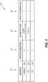
- Table 300illustrates three exemplary use cases in column 302.
- a first use case 310comprises camera use case.
- a second use case 312comprises a GPU use case.
- a third use casecomprises a CPU use case.
- the use caseman be identified by means of sub-cache partition, or by a master ID from each transaction.
- the DDR subsystem 122can then prefetch based on the use case's traffic pattern.
- the prefetch weighting valuecomprises a value that represents how aggressive the prefetch is to be applied to a cache prefetch function when an access pattern is detected (e.g., the value "0" being the least aggressive and a value "10" being the most aggressive).
- the access pattern 306defines the traffic request pattern from the corresponding use case. This represents the pattern used to detect and enable the prefetch, and the pattern that will be used to prefetch data.
- the prefetch patternis for every 256 bytes address granule ( i.e ., prefetch the first 64 bytes, skip the next 192bytes, then prefetch the first 64 bytes from the next 256 bytes unit).
- the delay tolerance 308represents how long a timing window the use case can handle for a request to get a response.
- Prefetch_size_nSize_pfch_max*Wn* F_ddr_max ⁇ F_ddr / F_ddr_max ⁇ F_ddr_min * 10
- Wnis the relative importance or weight of that client, measured in a percentage.
- Size_pfch_maxis the programmable maximum prefetch size to be issued from the DDR subsystem 122.
- Prefetch_size_nis the prefetched size for a use case in a particular use case, which may be based on, for example, the minimum granularity of cache operation.
- the DDR subsystem 122may adjust the system cache prefetch size based on the DDR frequency. For example, the prefetch size may be increased to mitigate latency when DRAM 104 is at a relatively lower frequency. The prefetch function may be disabled when the DDR frequency reaches a predetermined or programmable threshold. Furthermore, the DDR subsystem 122 may pre-configure the prefetch size according to, for example, a minimum size (e.g., 256 bytes) and a maximum size ( e.g ., 4Kbytes). The DDR subsystem 122 may control the prefetch size based on traffic patterns, the DDR frequency and prefetch hit rate.
- a minimum sizee.g., 256 bytes
- a maximum sizee.g ., 4Kbytes
- the DDR subsystem 122may adjust the system cache prefetch size the cache hit rates of the memory clients.
- the DDR subsystem 122may keep track of the cache lines that are allocated by the prefetch engine.
- the DDR subsystem 122may provide a separate counter for the cache lines allocated by prefetch and non-prefetch.
- the prefetch sizemay be increased when the cache hit rate on prefetched lines increases.
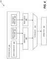
- FIG. 4is a combined block/flow diagram illustrating an embodiment of the system cache 128.
- the system cache 128comprises a write subcache 402 (e.g ., an exemplary write buffer 132), a write request pipeline 403, and a read miss pipeline 404.
- the write subcache 402 and the write request pipeline 403are coupled to a write queue 406.
- the read miss block 404is coupled to a read queue 408.
- the write queue 406 and the read queue 408communicate with a memory scheduler 410, which is coupled to the DRAM controller 130.
- FIG. 4illustrates the flow within one frequency point. In the case when DRAM 104 only supports one frequency point, the DRAM 104 may be switch between an active mode and a self-refresh mode.
- the DRAM controller 130can switch between clock gated and non-gated operation.
- FIG. 5illustrates a method 500 implemented in the system 400 of FIG. 4 .
- the DDR subsystem 122may be configured to a default condition comprising a default frequency and a default timeout The default condition may have a zero occupancy in the write subcache 402.
- the DDR subsystem 122may adjust the DDR frequency and/or prefetch size based on use case requirements.
- a timermay be used to put the DRAM 104 into the self-refresh mode when there is a lack of read/write activity.
- the write subcache 402may be used to extend the duration to keep DRAM 104 in the self-refresh mode to conserve power.
- the write requestmay be waiting in the write queue until the queue is full, and then the requests may be sent out together.
- the system 400may service a read request from the system cache 128 if there is a cache hit.
- the requestmay be temporarily put in a read request queue.
- the requestmay be waiting in the queue until the queue is full, and then the read requests may be sent out together. It should be appreciated, however, that when the request has, for example, a QoS priority higher than a configurable threshold, the request may be serviced without waiting in the read queue.
- the DRAM 104may be brought out of the self-refresh mode to service the request, such as a read miss, or when the write subcache 402 can no longer host the write request, the requests in the read queue and the write queue may be flushed out.
- FIG. 6is a flowchart illustrating another embodiment of the operation of the system cache 128.
- FIG. 6shows the detail within one frequency point or, in the case when DRAM 104 only supports one frequency point, how the write request is serviced to keep DRAM 104 in the self-refresh mode for as long as practical.
- the write subcache 402comprises a system cache partition.
- the cache lines that are not used as write subcache 402can be used as normal cache for use cases.
- Blocks 602, 604, 606, 608, and 610illustrate a non-cacheable request being received when DRAM 104 is in the active mode or in self-refresh. If the write queue 406 is not full, the request may be put in the queue to be scheduled for DDR I/O.
- DRAM 104If DRAM 104 is in the self-refresh mode or the queue is full, it will check the write subcache 402 at decision block 620.
- a cacheable write requestmay be processed through a normal cache operation, which may have different operation condition than the write buffer subcache.
- the systemdetermines if there is a cache hit or other cache lines need to be replaced.
- the victimis a dirty line, it goes to the same path above to decide whether to send the request to write subcache 402 or directly to the write queue 406.
- Blocks 620, 622, 624, and 626show the flow to allocate a cache line in the system cache 128 as write subcache 402 to temporarily buffer the data before it is written to DRAM 104.
- the DRAM 104is brought out of the self-refresh mode.
- FIG. 7is a combined block/flow diagram illustrating an embodiment of the operation of a QoS algorithm implemented in the scheduler of FIG. 4 .
- read requests 701 and write requests 703may reach the DDR subsystem 122 with a QoS indication, such as, a priority level.
- the requestsmay be serviced from the system cache 128, in which case a transaction to the DDR I/O is not generated. If there is a miss, the request is forwarded to the DDR IO.
- the requestmay be allocated in the system cache 128.
- a dirty cache linemay be evicted (line 702) to a different address to the DDR I/O.
- the address of the incoming request to the DDR subsystem 122may not be exactly the address on the DDR I/O.
- the address in the incoming read/write requests 701 and 703may not be the right information to be used for scheduling the traffic toward the DRAM CTLR 130.
- the system cache controller 710receives the write request 703 with address 0x1234ABCD.
- the system cache controller 710may determines that a new cache line will be allocated for this write request.
- the system cache controller 710may select a victim cache line to be evicted according to the replacement policy.
- Block 704shows the victim cache line with an address different than the original write request (e.g., 0x5555FFFF is going to be evicted to DDR).
- the evictiongenerates a write request for the address 0x5555FFFF.
- the requestis either put into the write queue 406 if the queue is not full, or put into the write subcache 402. Because of the write subcache, the DDR traffic scheduler 410 now has a bigger pool to be scheduled, including, for example, the following: (a) all the requests in the read queue with the QoS priority level of the request; (b) all the requests in the read queue with the QoS priority level of the request; and (c) all the requests in the write buffer.
- FIG. 8illustrates the system 100 incorporated in an exemplary portable computing device (PCD) 800.
- PCDportable computing device
- the SoC 322may include a multicore CPU 802.
- the multicore CPU 802may include a zeroth core 810, a first core 812, and an Nth core 814.
- One of the coresmay comprise, for example, a graphics processing unit (GPU) with one or more of the others comprising the CPU.
- GPUgraphics processing unit
- a display controller 328 and a touch screen controller 330may be coupled to the CPU 802.
- the touch screen display 606 external to the on-chip system 322may be coupled to the display controller 328 and the touch screen controller 330.
- FIG. 8further shows that a video encoder 334, e.g., a phase alternating line (PAL) encoder, a sequential color a memoire (SECAM) encoder, or a national television system(s) committee (NTSC) encoder, is coupled to the multicore CPU 802. Further, a video amplifier 336 is coupled to the video encoder 334 and the touch screen display 806. Also, a video port 338 is coupled to the video amplifier 336. As shown in FIG. 8 , a universal serial bus (USB) controller 340 is coupled to the multicore CPU 802. Also, a USB port 342 is coupled to the USB controller 340. Memory 104 and a subscriber identity module (SIM) card 346 may also be coupled to the multicore CPU 802.
- PALphase alternating line
- SECAMsequential color a memoire
- NTSCnational television system(s) committee
- a digital camera 348may be coupled to the multicore CPU 802.
- the digital camera 348is a charge-coupled device (CCD) camera or a complementary metal-oxide semiconductor (CMOS) camera.
- CCDcharge-coupled device
- CMOScomplementary metal-oxide semiconductor
- a stereo audio coder-decoder (CODEC) 350may be coupled to the multicore CPU 802.
- an audio amplifier 352may be coupled to the stereo audio CODEC 350.
- a first stereo speaker 354 and a second stereo speaker 356are coupled to the audio amplifier 352.
- FIG. 8shows that a microphone amplifier 358 may be also coupled to the stereo audio CODEC 350.
- a microphone 360may be coupled to the microphone amplifier 358.
- a frequency modulation (FM) radio tuner 362may be coupled to the stereo audio CODEC 350.
- an FM antenna 364is coupled to the FM radio tuner 362.
- stereo headphones 366may be coupled to the stereo audio CODEC 350.
- FMfrequency modulation
- FIG. 8further illustrates that a radio frequency (RF) transceiver 368 may be coupled to the multicore CPU 802.
- An RF switch 370may be coupled to the RF transceiver 368 and an RF antenna 372.
- a keypad 204may be coupled to the multicore CPU 802.
- a mono headset with a microphone 376may be coupled to the multicore CPU 802.
- a vibrator device 378may be coupled to the multicore CPU 802.
- FIG. 8also shows that a power supply 380 may be coupled to the on-chip system 322.
- the power supply 380is a direct current (DC) power supply that provides power to the various components of the PCD 800 that require power.
- the power supplyis a rechargeable DC battery or a DC power supply that is derived from an alternating current (AC) to DC transformer that is connected to an AC power source.
- ACalternating current
- FIG. 8further indicates that the PCD 800 may also include a network card 388 that may be used to access a data network, e.g., a local area network, a personal area network, or any other network.
- the network card 388may be a Bluetooth network card, a WiFi network card, a personal area network (PAN) card, a personal area network ultra-low-power technology (PeANUT) network card, a television/cable/satellite tuner, or any other network card well known in the art.
- the network card 388may be incorporated into a chip, i.e., the network card 388 may be a full solution in a chip, and may not be a separate network card 388.
- the touch screen display 806, the video port 338, the USB port 342, the camera 348, the first stereo speaker 354, the second stereo speaker 356, the microphone 360, the FM antenna 364, the stereo headphones 366, the RF switch 370, the RF antenna 372, the keypad 374, the mono headset 376, the vibrator 378, and the power supply 380may be external to the on-chip system 322.
- one or more of the method steps described hereinmay be stored in the memory as computer program instructions, such as the modules described above. These instructions may be executed by any suitable processor in combination or in concert with the corresponding module to perform the methods described herein.
- the functions describedmay be implemented in hardware, software, firmware, or any combination thereof. If implemented in software, the functions may be stored on or transmitted as one or more instructions or code on a computer-readable medium.
- Computer-readable mediainclude both computer storage media and communication media including any medium that facilitates transfer of a computer program from one place to another.
- a storage mediamay be any available media that may be accessed by a computer.
- such computer-readable mediamay comprise RAM, ROM, EEPROM, NAND flash, NOR flash, M-RAM, P-RAM, R-RAM, CD-ROM or other optical disk storage, magnetic disk storage or other magnetic storage devices, or any other medium that may be used to carry or store desired program code in the form of instructions or data structures and that may be accessed by a computer.
- any connectionis properly termed a computer-readable medium.
- the softwareis transmitted from a website, server, or other remote source using a coaxial cable, fiber optic cable, twisted pair, digital subscriber line ("DSL"), or wireless technologies such as infrared, radio, and microwave
- coaxial cable, fiber optic cable, twisted pair, DSL, or wireless technologiessuch as infrared, radio, and microwave are included in the definition of medium.
- Disk and discincludes compact disc (“CD”), laser disc, optical disc, digital versatile disc (“DVD”), floppy disk and blu-ray disc where disks usually reproduce data magnetically, while discs reproduce data optically with lasers. Combinations of the above should also be included within the scope of computer-readable media.
Landscapes
- Engineering & Computer Science (AREA)
- Theoretical Computer Science (AREA)
- Physics & Mathematics (AREA)
- General Engineering & Computer Science (AREA)
- General Physics & Mathematics (AREA)
- Human Computer Interaction (AREA)
- Power Sources (AREA)
- Memory System Of A Hierarchy Structure (AREA)
- Microelectronics & Electronic Packaging (AREA)
- Computer Hardware Design (AREA)
Description
- Portable computing devices (e.g., cellular telephones, smart phones, tablet computers, portable digital assistants (PDAs), portable game consoles, wearable devices, and other battery-powered devices) and other computing devices continue to offer an ever-expanding array of features and services, and provide users with unprecedented levels of access to information, resources, and communications. To keep pace with these service enhancements, such devices have become more powerful and more complex. Portable computing devices now commonly include a system on chip (SoC) comprising a plurality of memory clients embedded on a single substrate (e.g., one or more central processing units (CPUs), a graphics processing unit (GPU), digital signal processors,etc.). The memory clients may read data from and store data in a dynamic random access memory (DRAM) memory system electrically coupled to the SoC via a double data rate (DDR) bus.
- DDR system power is increasingly becoming a significant portion of total battery usage. Most of the DDR system power is a result of the read/write traffic to the DRAM. As systems become more complex, they demand higher traffic bandwidth and the traffic patterns become more complex and random, yielding increasing energy expenditure. Incorporating a last-level system cache may reduce the amount of DDR traffic. However, even with the benefit provided by the system cache, the DDR subsystem may still waste power because it must operate at a worst-case voltage and frequency required to service the unpredictable traffic. Existing solutions attempt to conserve DDR power by using an open-loop adjustment of the DDR clock frequency. These solutions, however, are sub-optimal because the adjustment must be conservative to avoid performance drops. While there is some power savings, further adjustments may compromise the end-user experience.
US 2001/011356 A1 discloses a memory clock control system and method that facilitates power reduction on a dynamic basis by detecting memory access request loading from a number of memory access devices, such as video and graphics engines. Based on the detected memory access requirements, the system and method adaptively varies a memory clock frequency in response to determining the desired memory usage at a given point in time.US 7,934,114 B2 discloses a method of controlling an information processing device which includes a processor having a cache memory, and a clock supplying unit that supplies a clock signal to the processor. The method includes: predicting a hit rate of the cache memory; and controlling the clock supplying unit so as to change a frequency of the clock signal in accordance with the predicted hit rate.- Accordingly, there is a need for improved systems and methods for reducing memory subsystem power.
- The invention is defined by the independent claims. Preferred embodiments of the invention are defined by the dependent claims.
- In the Figures, like reference numerals refer to like parts throughout the various views unless otherwise indicated. For reference numerals with letter character designations such as "102A" or "102B", the letter character designations may differentiate two like parts or elements present in the same Figure. Letter character designations for reference numerals may be omitted when it is intended that a reference numeral to encompass all parts having the same reference numeral in all Figures.
FIG. 1 is a block diagram of an embodiment of a system for reducing memory subsystem power.FIG. 2 is a flowchart illustrating an embodiment of a method for reducing power consumption of the DDR subsystem ofFIG. 1 .FIG. 3 is a table illustrating an exemplary embodiment of a method for adjusting prefetch size based on predetermined use cases.FIG. 4 is a combined block/flow diagram illustrating an embodiment of the system cache in the DDR subsystem ofFIG. 1 .FIG. 5 is a flowchart illustrating an embodiment of the operation of the write subcache in the system cache ofFIG. 4 .FIG. 6 is a flowchart illustrating another embodiment of the operation of the write subcache in the system cache ofFIG. 4 .FIG. 7 is a combined block/flow diagram illustrating an embodiment of the operation of a QoS algorithm implemented in the scheduler ofFIG. 4 .FIG. 8 is a block diagram of an embodiment of a portable communication device for incorporating the system ofFIG. 1 .- As used in this description, the terms "component," "module," "system," and the like are intended to refer to a computer-related entity, either hardware, firmware, a combination of hardware and software, software, or software in execution. A component may be localized on one computer and/or distributed between two or more computers. In addition, these components may execute from various computer readable media having various data structures stored thereon. The components may communicate by way of local and/or remote processes such as in accordance with a signal having one or more data packets (e.g., data from one component interacting with another component in a local system, distributed system, and/or across a network such as the Internet with other systems by way of the signal).
FIG. 1 illustrates an embodiment of asystem 100 for reducing memory subsystem power. Thesystem 100 may be implemented in any computing device, including a personal computer, a workstation, a server, or a portable computing device (PCD), such as a cellular telephone, a smart phone, a portable digital assistant (PDA), a portable game console, a tablet computer, or other battery-powered wearable device.- As illustrated in
FIG. 1 , thesystem 100 comprises a system on chip (SoC) 102 electrically coupled to a memory system via a memory bus. In the embodiment ofFIG. 1 , the memory system comprises a dynamic random access memory (DRAM) 104 coupled to theSoC 102 via a random access memory (RAM) bus 148 (e.g., a double data rate (DDR) bus). The SoC 102 comprises various on-chip components, including a plurality of memory clients, astorage controller 140, asystem resource manager 120, and a memory subsystem (e.g., DDR subsystem 122) interconnected via a SoC bus 118. The memory clients may comprise one or more processing units (e.g., a central processing unit (CPU) 106, a graphics processing unit (GPU) 108, a digital signal processor (DSP) 110, or other memory clients requesting read/write access to the memory system. Thesystem 100 further comprises a high-level operating system (HLOS) 116. - The
storage controller 140 controls the transfer of data to a storage device, such as, anon-volatile memory device 136. As further illustrated inFIG. 1 , theSoC 102 may comprise on-chip memory devices, such as, static random access memory (SRAM) 112 and read only memory (ROM) 114. - As described below in more detail, the
system 100 provides an improved architecture for enabling theDDR subsystem 122 to integrate complex memory traffic patterns and control the DDR clock frequency and/or voltage level to provide the overall performance requirements for various use cases. In operation, each of the memory clients may send a performance level vote to thesystem resource manager 120 via aninterface 142. As known in the art, the client votes indicate a desired memory bandwidth capability to the DDRsubsystem 122. Thesystem resource manager 120 comprises various functional blocks for managing system resources, such as, for example, clocks, voltage regulators, bus frequencies, quality of service, priority,etc. Thesystem resource manager 120 enables each component in thesystem 100 to vote for the state of system resources. Thesystem resource manager 120 may combine all of the client votes and estimate use case performance requirements. Thesystem resource manager 120 may forward the use case performance requirements to the DDRsubsystem 122 viainterface 144. The DDRsubsystem 122 controls its own clock frequency and voltage based on various local conditions under its control. - As illustrated in
FIG. 1 , the DDRsubsystem 122 comprises a local DDRSSresource manager 126 that receives the use case performance requirements from thesystem resource manager 120. In an embodiment, the localDDRSS resource manager 126 comprises a hardware block within the DDR subsystem. It should be appreciated that the local DDRSSresource manager 126 may comprise one or more functions implemented by, for example, one or more blocks within the DDRsubsystem 122. The localDDRSS resource manager 126 may control the DDR frequency via DDR clock controller 124. The localDDRSS resource manager 126 may control the DDR voltage by communicating with a power manager integrated circuit (IC) 138 electrically coupled to theSoC 102 via aconnection 146. In an embodiment, the DDR frequency and/or voltage may be adjusted based on the performance requirements of the memory clients and the cache hit rate of each client. - As further illustrated in
FIG. 1 , the DDRsubsystem 122 comprises asystem cache 128, and may furthermore comprise one or morecache performance monitors 134, and aDRAM controller 130. Thesystem cache 128 is electrically coupled to theDRAM controller 130. TheDRAM controller 130 is electrically coupled to the off-chip DRAM 104 via theRAM bus 148. Thesystem cache 128 may comprise a shared or last-level cache comprising awrite buffer 132. Thesystem cache 128 is a component that stores data so future requests for that data can be served faster. In an embodiment, thesystem cache 128 may reside externally outside of theSoC 102 and connect to theSoC 102 via an I/O bus. - In another embodiment, the
DDR subsystem 122 may control the DDR voltage and/or frequency based on client-specific performance monitors 134 and/or the cache hit rate of each memory client. It should be appreciated that the clock frequency and voltage of the DDR and thesystem cache 128 may be separately controlled. As described below in more detail, theDDR subsystem 122 may use thewrite buffer 132 to aggregate and more effectively schedule write access toDRAM 104. Furthermore, theDDR subsystem 122 applies various cache prefetch policies to aggregate read access and mitigate latency whenDRAM 104 is operating at relatively low frequency (e.g., below a predetermined or programmable level). - It should be appreciated that
DDR subsystem 122 may use the cache hit rates together with the client votes as input elements for calculation of the DDR clock frequency and, thereby, maintain the DDR clock frequency at a more optimal level. Furthermore, reducing the clock frequency also allows the voltage to be reduced, which results in an overall energy savings. FIG. 2 is a flowchart illustrating an embodiment of amethod 200 implemented insystem 100 for adjusting the DDR frequency. Themethod 200 may be performed for various different use cases. Atblock 202, a use case may be initiated or resumed. Atblock 204, thesystem 100 may initially have default frequency and/or voltage levels for thesystem cache 128 andDRAM 104. Thesystem resource manager 120 receives initial performance level votes from the memory clients (e.g.,CPU 106, GPU 108, DSP 110,etc.). Atblock 206, thesystem resource manager 120 determines memory performance requirements based on the performance level votes received from the memory clients. In an embodiment, thesystem resource manager 120 estimates the performance requirements. Thesystem resource manager 120 may use quality of service (QoS) information to update the performance estimates. Atblock 208, the memory performance requirements are sent to theDDR subsystem 122. The memory performance requirements may be forwarded to the localDDRSS resource manager 126 via interface 144 (FIG. 1 .). Atblock 210, the localDDRSS resource manager 126 may calculate and adjust the frequency and/or voltage for the DDR clock controller 124 and thesystem cache 128 based on the cache hit rates of the memory clients. As mentioned above, the cache hit rates may be determined by one or more performance monitors 134. The localDDRSS resource manager 126 may also adjust a system cache prefetch size based on the cache hit rates and the memory performance requirements. In an exemplary embodiment, the clock frequency for each of a plurality of memory clients (e.g., client 0 - client n) may be assigned a predetermined weight (Wn). The predetermined weights (Wn) may be pre-calibrated for each client with a unique bandwidth requirement (BWn) and a hit rate (HRn). The total bandwidth requirement to thesystem cache 128 comprises a sum of all clients' bandwidth requirements (BWn) normalized by the corresponding client's weight and cache hit rate. The system cache frequency may be determined by dividing the system cache's total bandwidth requirement by the width of the system cache's data path.- The DDR frequency may be calculated in a similar manner by the cache miss rate instead of the cache hit rate, as shown in Equations 1 and 2 below.


- In this simplified design, the DDR frequency may comprise a fixed value regardless of the plurality of memory client bandwidth requirements and cache hit rates. The fixed value may be selected from a set of predefined frequencies assuming worst case cache hit rate and concurrent condition.
- It should be appreciated that the
DDR subsystem 122 may adjust memory access patterns to theDRAM 104 based on, for example, the cache hit rates of the plurality of memory clients, the DDR operating frequency, and the clients' access pattern. Referring toFIG. 3 , in one embodiment, theDDR subsystem 122 may adjust the system cache prefetch size based on one or more use cases. Table 300 illustrates three exemplary use cases incolumn 302. Afirst use case 310 comprises camera use case. Asecond use case 312 comprises a GPU use case. A third use case comprises a CPU use case. The use case man be identified by means of sub-cache partition, or by a master ID from each transaction. TheDDR subsystem 122 can then prefetch based on the use case's traffic pattern.Columns DDR subsystem 122, which may be set to a pre-tuned value for each use case. The prefetch weighting value comprises a value that represents how aggressive the prefetch is to be applied to a cache prefetch function when an access pattern is detected (e.g., the value "0" being the least aggressive and a value "10" being the most aggressive). - The access pattern 306 (
FIG. 3 ) defines the traffic request pattern from the corresponding use case. This represents the pattern used to detect and enable the prefetch, and the pattern that will be used to prefetch data. For acamera use case 310, the prefetch pattern is for every 256 bytes address granule (i.e., prefetch the first 64 bytes, skip the next 192bytes, then prefetch the first 64 bytes from the next 256 bytes unit). Thedelay tolerance 308 represents how long a timing window the use case can handle for a request to get a response. This information may be helpful in guiding the DDR subsystem 122 (e.g., controlling how much it can hold off the I/O request toward the DRAM, and keep the DRAM and I/O in low power state as long as possible). Once a prefetch action is needed for a use case, the prefetch size for that use case may be determined according to Equation 3.
DDR subsystem 122. "Prefetch_size_n" is the prefetched size for a use case in a particular use case, which may be based on, for example, the minimum granularity of cache operation. - In another embodiment, the
DDR subsystem 122 may adjust the system cache prefetch size based on the DDR frequency. For example, the prefetch size may be increased to mitigate latency whenDRAM 104 is at a relatively lower frequency. The prefetch function may be disabled when the DDR frequency reaches a predetermined or programmable threshold. Furthermore, theDDR subsystem 122 may pre-configure the prefetch size according to, for example, a minimum size (e.g., 256 bytes) and a maximum size (e.g., 4Kbytes). TheDDR subsystem 122 may control the prefetch size based on traffic patterns, the DDR frequency and prefetch hit rate. - In a further embodiment, the
DDR subsystem 122 may adjust the system cache prefetch size the cache hit rates of the memory clients. TheDDR subsystem 122 may keep track of the cache lines that are allocated by the prefetch engine. When monitoring cache hit rate, theDDR subsystem 122 may provide a separate counter for the cache lines allocated by prefetch and non-prefetch. The prefetch size may be increased when the cache hit rate on prefetched lines increases. FIG. 4 is a combined block/flow diagram illustrating an embodiment of thesystem cache 128. Thesystem cache 128 comprises a write subcache 402 (e.g., an exemplary write buffer 132), awrite request pipeline 403, and aread miss pipeline 404. Thewrite subcache 402 and thewrite request pipeline 403 are coupled to awrite queue 406. The readmiss block 404 is coupled to aread queue 408. Thewrite queue 406 and theread queue 408 communicate with amemory scheduler 410, which is coupled to theDRAM controller 130. It should be appreciated thatFIG. 4 illustrates the flow within one frequency point. In the case whenDRAM 104 only supports one frequency point, theDRAM 104 may be switch between an active mode and a self-refresh mode. TheDRAM controller 130 can switch between clock gated and non-gated operation.FIG. 5 illustrates amethod 500 implemented in thesystem 400 ofFIG. 4 . During boot, atblock 502, theDDR subsystem 122 may be configured to a default condition comprising a default frequency and a default timeout The default condition may have a zero occupancy in thewrite subcache 402. Atblock 504, theDDR subsystem 122 may adjust the DDR frequency and/or prefetch size based on use case requirements. Atblocks DRAM 104 into the self-refresh mode when there is a lack of read/write activity. Atblock 516, for a write request, thewrite subcache 402 may be used to extend the duration to keepDRAM 104 in the self-refresh mode to conserve power. The write request may be waiting in the write queue until the queue is full, and then the requests may be sent out together. Atblocks system 400 may service a read request from thesystem cache 128 if there is a cache hit. Upon a read miss, the request may be temporarily put in a read request queue. In order to aggregate the read access, the request may be waiting in the queue until the queue is full, and then the read requests may be sent out together. It should be appreciated, however, that when the request has, for example, a QoS priority higher than a configurable threshold, the request may be serviced without waiting in the read queue. Atblock 518, theDRAM 104 may be brought out of the self-refresh mode to service the request, such as a read miss, or when thewrite subcache 402 can no longer host the write request, the requests in the read queue and the write queue may be flushed out.FIG. 6 is a flowchart illustrating another embodiment of the operation of thesystem cache 128.FIG. 6 shows the detail within one frequency point or, in the case whenDRAM 104 only supports one frequency point, how the write request is serviced to keepDRAM 104 in the self-refresh mode for as long as practical. Thewrite subcache 402 comprises a system cache partition. The cache lines that are not used aswrite subcache 402 can be used as normal cache for use cases.Blocks DRAM 104 is in the active mode or in self-refresh. If thewrite queue 406 is not full, the request may be put in the queue to be scheduled for DDR I/O. If DRAM 104 is in the self-refresh mode or the queue is full, it will check thewrite subcache 402 atdecision block 620. A cacheable write request may be processed through a normal cache operation, which may have different operation condition than the write buffer subcache. Atblocks block 618, if there is a cache miss and the victim is a dirty line, it goes to the same path above to decide whether to send the request to write subcache 402 or directly to thewrite queue 406.Blocks system cache 128 aswrite subcache 402 to temporarily buffer the data before it is written toDRAM 104. Atblocks write subcache 402, theDRAM 104 is brought out of the self-refresh mode.FIG. 7 is a combined block/flow diagram illustrating an embodiment of the operation of a QoS algorithm implemented in the scheduler ofFIG. 4 . As illustrated inFIG. 7 , readrequests 701 and writerequests 703 may reach theDDR subsystem 122 with a QoS indication, such as, a priority level. The requests may be serviced from thesystem cache 128, in which case a transaction to the DDR I/O is not generated. If there is a miss, the request is forwarded to the DDR IO. The request may be allocated in thesystem cache 128. A dirty cache line may be evicted (line 702) to a different address to the DDR I/O. Therefore, the address of the incoming request to theDDR subsystem 122 may not be exactly the address on the DDR I/O. The address in the incoming read/write requests DRAM CTLR 130. In this example, thesystem cache controller 710 receives thewrite request 703 with address 0x1234ABCD. Thesystem cache controller 710 may determines that a new cache line will be allocated for this write request. As illustrated atline 702, thesystem cache controller 710 may select a victim cache line to be evicted according to the replacement policy.Block 704 shows the victim cache line with an address different than the original write request (e.g., 0x5555FFFF is going to be evicted to DDR). Atblock 132, the eviction generates a write request for the address 0x5555FFFF. The request is either put into thewrite queue 406 if the queue is not full, or put into thewrite subcache 402. Because of the write subcache, theDDR traffic scheduler 410 now has a bigger pool to be scheduled, including, for example, the following: (a) all the requests in the read queue with the QoS priority level of the request; (b) all the requests in the read queue with the QoS priority level of the request; and (c) all the requests in the write buffer. Having visibility of more incoming traffic allows the scheduler for better scheduling, with the scheduling criteria considering the request's QoS priority level, DRAM page open and bank hit, read priority over write priority, etc., and send the request to theDRAM controller 130. In this manner, it should be appreciated that system can have better QoS and DDR utilization by providing the scheduler with bigger pool for scheduling.- As mentioned above, the
system 100 may be incorporated into any desirable computing system.FIG. 8 illustrates thesystem 100 incorporated in an exemplary portable computing device (PCD) 800. It will be readily appreciated that certain components of the system 100 (e.g., RPM 116) are included on the SoC 322 (FIG. 8 ) while other components (e.g., the DRAM 104) are external components coupled to theSoC 322. TheSoC 322 may include amulticore CPU 802. Themulticore CPU 802 may include azeroth core 810, afirst core 812, and anNth core 814. One of the cores may comprise, for example, a graphics processing unit (GPU) with one or more of the others comprising the CPU. - A
display controller 328 and atouch screen controller 330 may be coupled to theCPU 802. In turn, thetouch screen display 606 external to the on-chip system 322 may be coupled to thedisplay controller 328 and thetouch screen controller 330. FIG. 8 further shows that avideo encoder 334, e.g., a phase alternating line (PAL) encoder, a sequential color a memoire (SECAM) encoder, or a national television system(s) committee (NTSC) encoder, is coupled to themulticore CPU 802. Further, avideo amplifier 336 is coupled to thevideo encoder 334 and thetouch screen display 806. Also, avideo port 338 is coupled to thevideo amplifier 336. As shown inFIG. 8 , a universal serial bus (USB)controller 340 is coupled to themulticore CPU 802. Also, aUSB port 342 is coupled to theUSB controller 340.Memory 104 and a subscriber identity module (SIM)card 346 may also be coupled to themulticore CPU 802.- Further, as shown in
FIG. 8 , adigital camera 348 may be coupled to themulticore CPU 802. In an exemplary aspect, thedigital camera 348 is a charge-coupled device (CCD) camera or a complementary metal-oxide semiconductor (CMOS) camera. - As further illustrated in
FIG. 8 , a stereo audio coder-decoder (CODEC) 350 may be coupled to themulticore CPU 802. Moreover, anaudio amplifier 352 may be coupled to thestereo audio CODEC 350. In an exemplary aspect, afirst stereo speaker 354 and asecond stereo speaker 356 are coupled to theaudio amplifier 352.FIG. 8 shows that amicrophone amplifier 358 may be also coupled to thestereo audio CODEC 350. Additionally, amicrophone 360 may be coupled to themicrophone amplifier 358. In a particular aspect, a frequency modulation (FM)radio tuner 362 may be coupled to thestereo audio CODEC 350. Also, anFM antenna 364 is coupled to theFM radio tuner 362. Further,stereo headphones 366 may be coupled to thestereo audio CODEC 350. FIG. 8 further illustrates that a radio frequency (RF)transceiver 368 may be coupled to themulticore CPU 802. AnRF switch 370 may be coupled to theRF transceiver 368 and an RF antenna 372. Akeypad 204 may be coupled to themulticore CPU 802. Also, a mono headset with amicrophone 376 may be coupled to themulticore CPU 802. Further, avibrator device 378 may be coupled to themulticore CPU 802.FIG. 8 also shows that apower supply 380 may be coupled to the on-chip system 322. In a particular aspect, thepower supply 380 is a direct current (DC) power supply that provides power to the various components of thePCD 800 that require power. Further, in a particular aspect, the power supply is a rechargeable DC battery or a DC power supply that is derived from an alternating current (AC) to DC transformer that is connected to an AC power source.FIG. 8 further indicates that thePCD 800 may also include anetwork card 388 that may be used to access a data network, e.g., a local area network, a personal area network, or any other network. Thenetwork card 388 may be a Bluetooth network card, a WiFi network card, a personal area network (PAN) card, a personal area network ultra-low-power technology (PeANUT) network card, a television/cable/satellite tuner, or any other network card well known in the art. Further, thenetwork card 388 may be incorporated into a chip,i.e., thenetwork card 388 may be a full solution in a chip, and may not be aseparate network card 388.- As depicted in
FIG. 8 , thetouch screen display 806, thevideo port 338, theUSB port 342, thecamera 348, thefirst stereo speaker 354, thesecond stereo speaker 356, themicrophone 360, theFM antenna 364, thestereo headphones 366, theRF switch 370, the RF antenna 372, the keypad 374, themono headset 376, thevibrator 378, and thepower supply 380 may be external to the on-chip system 322. - It should be appreciated that one or more of the method steps described herein may be stored in the memory as computer program instructions, such as the modules described above. These instructions may be executed by any suitable processor in combination or in concert with the corresponding module to perform the methods described herein.
- Additionally, one of ordinary skill in programming is able to write computer code or identify appropriate hardware and/or circuits to implement the disclosed invention without difficulty based on the flow charts and associated description in this specification, for example.
- Therefore, disclosure of a particular set of program code instructions or detailed hardware devices is not considered necessary for an adequate understanding of how to make and use the invention. The inventive functionality of the claimed computer implemented processes is explained in more detail in the above description and in conjunction with the Figures which may illustrate various process flows.
- In one or more exemplary aspects, the functions described may be implemented in hardware, software, firmware, or any combination thereof. If implemented in software, the functions may be stored on or transmitted as one or more instructions or code on a computer-readable medium. Computer-readable media include both computer storage media and communication media including any medium that facilitates transfer of a computer program from one place to another. A storage media may be any available media that may be accessed by a computer. By way of example, and not limitation, such computer-readable media may comprise RAM, ROM, EEPROM, NAND flash, NOR flash, M-RAM, P-RAM, R-RAM, CD-ROM or other optical disk storage, magnetic disk storage or other magnetic storage devices, or any other medium that may be used to carry or store desired program code in the form of instructions or data structures and that may be accessed by a computer.
- Also, any connection is properly termed a computer-readable medium. For example, if the software is transmitted from a website, server, or other remote source using a coaxial cable, fiber optic cable, twisted pair, digital subscriber line ("DSL"), or wireless technologies such as infrared, radio, and microwave, then the coaxial cable, fiber optic cable, twisted pair, DSL, or wireless technologies such as infrared, radio, and microwave are included in the definition of medium.
- Disk and disc, as used herein, includes compact disc ("CD"), laser disc, optical disc, digital versatile disc ("DVD"), floppy disk and blu-ray disc where disks usually reproduce data magnetically, while discs reproduce data optically with lasers. Combinations of the above should also be included within the scope of computer-readable media.


Claims (15)
- A method for reducing memory subsystem power, the method comprising:a system resource manager (120) determining memory performance requirements for a plurality of memory clients and providing the memory performance requirements to a double data rate, DDR, subsystem (122), the DDR subsystem (122) and the system resource manager (120) residing on a system on chip, SoC, (102) electrically coupled to a dynamic random access memory, DRAM, (104);determining with the DDR subsystem (122) a cache hit rate of each of the plurality of memory clients associated with a system cache (128) residing on the DDR subsystem (122);the DDR subsystem (122) controlling a DDR clock frequency based on the memory performance requirements received from the system resource manager (120) and the cache hit rates of the plurality of memory clients; andthe DDR subsystem (122) applying cache prefetch policies to aggregate read access when the DRAM (104) is operating at a frequency below a predetermined or programmable level.
- The method of claim 1, further comprising:
the system resource manager (120) receiving a performance level vote from each of the plurality of memory clients, the performance level votes indicating a desired memory bandwidth. - The method of claim 2, wherein the system resource manager (120) determines the memory performance requirements based on the performance level votes received from the plurality of memory clients.
- The method of claim 1, wherein the DDR subsystem (122) comprises a local resource manager for controlling the DDR clock frequency.
- The method of claim 4, wherein the local resource manager comprises a dedicated block in the DDR subsystem (122).
- The method of claim 1, wherein the memory clients comprise one or more of a central processing unit, CPU, a graphics processing unit, GPU, and a digital signal processor ,DSP, electrically coupled via a SoC (102) bus.
- The method of claim 1, wherein the DDR subsystem (122) further comprises a one or more performance monitors for determining the cache hit rates of each of the plurality of memory clients.
- A system for reducing memory subsystem power, the system comprising:means for determining memory performance requirements for a plurality of memory clients and providing the memory performance requirements to a double data rate, DDR, subsystem (122), the DDR subsystem (122) residing on a system on chip, SoC, (102) electrically coupled to a dynamic random access memory, DRAM, (104);means for determining at the DDR subsystem (122) a cache hit rate of each of the plurality of memory clients associated with a system cache (128) residing on the DDR subsystem (122);means for the DDR subsystem (122) to control a DDR clock frequency based on the memory performance requirements and the cache hit rates of the plurality of memory clients; andmeans for the DDR subsystem (122) to apply cache prefetch policies to aggregate read access when the DRAM (104) is operating at a frequency below a predetermined or programmable level.
- The system of claim 8, further comprising:
means for receiving a performance level vote from each of the plurality of memory clients, the performance level votes indicating a desired memory bandwidth. - The system of claim 9, wherein the memory performance requirements are determined based on the performance level votes received from the plurality of memory clients.
- The system of claim 9, wherein at least one of the performance level votes is lowered based on the corresponding cache hit rate.
- The system of claim 8, wherein the means for controlling the DDR clock frequency comprises a local resource manager residing on the DDR subsystem (122).
- The system of claim 8, wherein the memory clients comprise one or more of a central processing unit, CPU, a graphics processing unit, GPU, and a digital signal processor, DSP, electrically coupled via a SoC (102) bus.
- The system of claim 8, wherein the means for determining the cache hit rates of each of the plurality of memory clients comprise one or more performance monitors residing on the DDR subsystem (122).
- A computer program comprising instructions which, when the program is executed by a computer, cause the computer to carry out the method of any of the claims 1-7.
Applications Claiming Priority (2)
| Application Number | Priority Date | Filing Date | Title |
|---|---|---|---|
| US15/081,914US9778871B1 (en) | 2016-03-27 | 2016-03-27 | Power-reducing memory subsystem having a system cache and local resource management |
| PCT/US2017/020810WO2017172267A1 (en) | 2016-03-27 | 2017-03-03 | Power-reducing memory subsystem having a system cache and local resource management |
Publications (2)
| Publication Number | Publication Date |
|---|---|
| EP3436959A1 EP3436959A1 (en) | 2019-02-06 |
| EP3436959B1true EP3436959B1 (en) | 2023-05-10 |
Family
ID=58358940
Family Applications (1)
| Application Number | Title | Priority Date | Filing Date |
|---|---|---|---|
| EP17711940.1AActiveEP3436959B1 (en) | 2016-03-27 | 2017-03-03 | Power-reducing memory subsystem having a system cache and local resource management |
Country Status (4)
| Country | Link |
|---|---|
| US (1) | US9778871B1 (en) |
| EP (1) | EP3436959B1 (en) |
| CN (1) | CN109074331B (en) |
| WO (1) | WO2017172267A1 (en) |
Families Citing this family (17)
| Publication number | Priority date | Publication date | Assignee | Title |
|---|---|---|---|---|
| US10719902B2 (en)* | 2017-04-17 | 2020-07-21 | Intel Corporation | Thread serialization, distributed parallel programming, and runtime extensions of parallel computing platform |
| US10409614B2 (en) | 2017-04-24 | 2019-09-10 | Intel Corporation | Instructions having support for floating point and integer data types in the same register |
| US10474458B2 (en) | 2017-04-28 | 2019-11-12 | Intel Corporation | Instructions and logic to perform floating-point and integer operations for machine learning |
| EP3650464A4 (en) | 2017-07-05 | 2021-01-13 | XDCExplorer (Shanghai) Co., Ltd. | PEPTIDE COMPOUND AND ITS APPLICATION AND A COMPOSITION WITH THE PEPTIDE COMPOUND |
| EP3938893B1 (en) | 2019-03-15 | 2025-10-15 | Intel Corporation | Systems and methods for cache optimization |
| US11934342B2 (en) | 2019-03-15 | 2024-03-19 | Intel Corporation | Assistance for hardware prefetch in cache access |
| CN113383310A (en) | 2019-03-15 | 2021-09-10 | 英特尔公司 | Pulse decomposition within matrix accelerator architecture |
| EP3938913A1 (en) | 2019-03-15 | 2022-01-19 | INTEL Corporation | Multi-tile architecture for graphics operations |
| US11861761B2 (en) | 2019-11-15 | 2024-01-02 | Intel Corporation | Graphics processing unit processing and caching improvements |
| US11551730B2 (en)* | 2021-01-26 | 2023-01-10 | Qualcomm Incorporated | Low power memory system using dual input-output voltage supplies |
| KR20230011595A (en)* | 2021-07-14 | 2023-01-25 | 에스케이하이닉스 주식회사 | System and operating method of system |
| CN114201438A (en)* | 2021-12-08 | 2022-03-18 | 北京奕斯伟计算技术有限公司 | Clock frequency management method, system and integrated device |
| US12174747B2 (en)* | 2021-12-20 | 2024-12-24 | Advanced Micro Devices, Inc. | Last level cache access during non-Cstate self refresh |
| US11966338B2 (en)* | 2022-07-19 | 2024-04-23 | International Business Machines Corporation | Prefetching management in database system based on number of pages being prefetched |
| EP4350480A4 (en)* | 2022-08-24 | 2024-10-16 | Samsung Electronics Co., Ltd. | ELECTRONIC DEVICE, METHOD AND COMPUTER-READABLE STORAGE MEDIUM FOR ADJUSTING THE FREQUENCIES OF EACH CIRCUIT CONTAINED IN A PROCESSOR |
| US12265712B2 (en)* | 2023-08-09 | 2025-04-01 | Qualcomm Incorporated | Dynamic DDR scaling and use case management based on DDR refresh rate and size |
| US20250103479A1 (en)* | 2023-09-27 | 2025-03-27 | Qualcomm Incorporated | Dynamic Random-Access Memory (DRAM) Efficiency Calculation and Utilization of Last Level Cache (LLC) |
Family Cites Families (21)
| Publication number | Priority date | Publication date | Assignee | Title |
|---|---|---|---|---|
| US5860106A (en) | 1995-07-13 | 1999-01-12 | Intel Corporation | Method and apparatus for dynamically adjusting power/performance characteristics of a memory subsystem |
| US6460125B2 (en)* | 1998-08-07 | 2002-10-01 | Ati Technologies, Inc. | Dynamic memory clock control system and method |
| US6334167B1 (en) | 1998-08-31 | 2001-12-25 | International Business Machines Corporation | System and method for memory self-timed refresh for reduced power consumption |
| US7032076B2 (en)* | 2002-09-16 | 2006-04-18 | Intel Corporation | Prefetching data in a computer system |
| JP4555145B2 (en)* | 2005-04-28 | 2010-09-29 | 富士通株式会社 | Batch scheduling program, batch scheduling method, and batch scheduling apparatus |
| US20070043965A1 (en) | 2005-08-22 | 2007-02-22 | Intel Corporation | Dynamic memory sizing for power reduction |
| JP4837456B2 (en)* | 2006-06-28 | 2011-12-14 | パナソニック株式会社 | Information processing device |
| US20090204837A1 (en) | 2008-02-11 | 2009-08-13 | Udaykumar Raval | Power control system and method |
| US8589707B2 (en) | 2008-12-05 | 2013-11-19 | Stmicroelectronics International N.V. | System and method for optimizing electrical power consumption by changing CPU frequency including steps of changing the system to a slow mode, changing a phase locked loop frequency register and changing the system to a normal mode |
| US8656198B2 (en) | 2010-04-26 | 2014-02-18 | Advanced Micro Devices | Method and apparatus for memory power management |
| US8339891B2 (en) | 2010-05-25 | 2012-12-25 | Lsi Corporation | Power savings and/or dynamic power management in a memory |
| US8438410B2 (en)* | 2010-06-23 | 2013-05-07 | Intel Corporation | Memory power management via dynamic memory operation states |
| JP2012150529A (en) | 2011-01-17 | 2012-08-09 | Sony Corp | Memory access control circuit, prefetch circuit, memory device, and information processing system |
| US8621157B2 (en)* | 2011-06-13 | 2013-12-31 | Advanced Micro Devices, Inc. | Cache prefetching from non-uniform memories |
| US20120095607A1 (en) | 2011-12-22 | 2012-04-19 | Wells Ryan D | Method, Apparatus, and System for Energy Efficiency and Energy Conservation Through Dynamic Management of Memory and Input/Output Subsystems |
| US8713256B2 (en) | 2011-12-23 | 2014-04-29 | Intel Corporation | Method, apparatus, and system for energy efficiency and energy conservation including dynamic cache sizing and cache operating voltage management for optimal power performance |
| US9201796B2 (en)* | 2012-09-27 | 2015-12-01 | Apple Inc. | System cache with speculative read engine |
| US9575542B2 (en)* | 2013-01-31 | 2017-02-21 | Hewlett Packard Enterprise Development Lp | Computer power management |
| US9430031B2 (en)* | 2013-07-29 | 2016-08-30 | Western Digital Technologies, Inc. | Power conservation based on caching |
| US9547331B2 (en)* | 2014-04-03 | 2017-01-17 | Qualcomm Incorporated | Apparatus and method to set the speed of a clock |
| KR20160063974A (en)* | 2014-11-27 | 2016-06-07 | 삼성전자주식회사 | System on chip for controlling power using workload, method thereof, and computing device having the same |
- 2016
- 2016-03-27USUS15/081,914patent/US9778871B1/enactiveActive
- 2017
- 2017-03-03EPEP17711940.1Apatent/EP3436959B1/enactiveActive
- 2017-03-03WOPCT/US2017/020810patent/WO2017172267A1/ennot_activeCeased
- 2017-03-03CNCN201780019649.XApatent/CN109074331B/enactiveActive
Also Published As
| Publication number | Publication date |
|---|---|
| CN109074331B (en) | 2022-03-22 |
| WO2017172267A1 (en) | 2017-10-05 |
| EP3436959A1 (en) | 2019-02-06 |
| US9778871B1 (en) | 2017-10-03 |
| CN109074331A (en) | 2018-12-21 |
| US20170277460A1 (en) | 2017-09-28 |
Similar Documents
| Publication | Publication Date | Title |
|---|---|---|
| EP3436959B1 (en) | Power-reducing memory subsystem having a system cache and local resource management | |
| EP3436956B1 (en) | Power-reducing memory subsystem having a system cache and local resource management | |
| US9697124B2 (en) | Systems and methods for providing dynamic cache extension in a multi-cluster heterogeneous processor architecture | |
| US7971074B2 (en) | Method, system, and apparatus for a core activity detector to facilitate dynamic power management in a distributed system | |
| US6889330B2 (en) | Dynamic hardware configuration for energy management systems using task attributes | |
| US20170024316A1 (en) | Systems and methods for scheduling tasks in a heterogeneous processor cluster architecture using cache demand monitoring | |
| US7281148B2 (en) | Power managed busses and arbitration | |
| US10831254B2 (en) | Allocating power between multiple central processing units (CPUs) in a multi-CPU processor based on total current availability and individual CPU quality-of-service (QoS) requirements | |
| EP1182548A2 (en) | Dynamic hardware control for energy management systems using task attributes | |
| US9703493B2 (en) | Single-stage arbiter/scheduler for a memory system comprising a volatile memory and a shared cache | |
| US20170212581A1 (en) | Systems and methods for providing power efficiency via memory latency control | |
| US11620243B2 (en) | Way partitioning for a system-level cache | |
| US10067691B1 (en) | System and method for dynamic control of shared memory management resources | |
| US20140129778A1 (en) | Multi-Port Shared Cache Apparatus | |
| KR20160018204A (en) | Electronic device, On-Chip memory and operating method of the on-chip memory | |
| CA2832223C (en) | Multi-port shared cache apparatus | |
| US20240330061A1 (en) | Systems and methods for prioritizing and assigning threads in a heterogeneous processor architecture |
Legal Events
| Date | Code | Title | Description |
|---|---|---|---|
| STAA | Information on the status of an ep patent application or granted ep patent | Free format text:STATUS: UNKNOWN | |
| STAA | Information on the status of an ep patent application or granted ep patent | Free format text:STATUS: THE INTERNATIONAL PUBLICATION HAS BEEN MADE | |
| PUAI | Public reference made under article 153(3) epc to a published international application that has entered the european phase | Free format text:ORIGINAL CODE: 0009012 | |
| STAA | Information on the status of an ep patent application or granted ep patent | Free format text:STATUS: REQUEST FOR EXAMINATION WAS MADE | |
| 17P | Request for examination filed | Effective date:20181010 | |
| AK | Designated contracting states | Kind code of ref document:A1 Designated state(s):AL AT BE BG CH CY CZ DE DK EE ES FI FR GB GR HR HU IE IS IT LI LT LU LV MC MK MT NL NO PL PT RO RS SE SI SK SM TR | |
| AX | Request for extension of the european patent | Extension state:BA ME | |
| DAV | Request for validation of the european patent (deleted) | ||
| DAX | Request for extension of the european patent (deleted) | ||
| STAA | Information on the status of an ep patent application or granted ep patent | Free format text:STATUS: EXAMINATION IS IN PROGRESS | |
| 17Q | First examination report despatched | Effective date:20200723 | |
| GRAP | Despatch of communication of intention to grant a patent | Free format text:ORIGINAL CODE: EPIDOSNIGR1 | |
| STAA | Information on the status of an ep patent application or granted ep patent | Free format text:STATUS: GRANT OF PATENT IS INTENDED | |
| INTG | Intention to grant announced | Effective date:20220110 | |
| GRAJ | Information related to disapproval of communication of intention to grant by the applicant or resumption of examination proceedings by the epo deleted | Free format text:ORIGINAL CODE: EPIDOSDIGR1 | |
| STAA | Information on the status of an ep patent application or granted ep patent | Free format text:STATUS: EXAMINATION IS IN PROGRESS | |
| INTC | Intention to grant announced (deleted) | ||
| RIC1 | Information provided on ipc code assigned before grant | Ipc:G11C 11/406 20060101ALI20221107BHEP Ipc:G06F 1/3296 20190101ALI20221107BHEP Ipc:G06F 1/3234 20190101ALI20221107BHEP Ipc:G06F 1/324 20190101ALI20221107BHEP Ipc:G06F 1/32 20190101ALI20221107BHEP Ipc:G06F 13/16 20060101AFI20221107BHEP | |
| GRAP | Despatch of communication of intention to grant a patent | Free format text:ORIGINAL CODE: EPIDOSNIGR1 | |
| STAA | Information on the status of an ep patent application or granted ep patent | Free format text:STATUS: GRANT OF PATENT IS INTENDED | |
| INTG | Intention to grant announced | Effective date:20221220 | |
| GRAS | Grant fee paid | Free format text:ORIGINAL CODE: EPIDOSNIGR3 | |
| GRAA | (expected) grant | Free format text:ORIGINAL CODE: 0009210 | |
| STAA | Information on the status of an ep patent application or granted ep patent | Free format text:STATUS: THE PATENT HAS BEEN GRANTED | |
| AK | Designated contracting states | Kind code of ref document:B1 Designated state(s):AL AT BE BG CH CY CZ DE DK EE ES FI FR GB GR HR HU IE IS IT LI LT LU LV MC MK MT NL NO PL PT RO RS SE SI SK SM TR | |
| REG | Reference to a national code | Ref country code:GB Ref legal event code:FG4D | |
| REG | Reference to a national code | Ref country code:AT Ref legal event code:REF Ref document number:1567401 Country of ref document:AT Kind code of ref document:T Effective date:20230515 Ref country code:CH Ref legal event code:EP | |
| REG | Reference to a national code | Ref country code:DE Ref legal event code:R096 Ref document number:602017068558 Country of ref document:DE | |
| REG | Reference to a national code | Ref country code:IE Ref legal event code:FG4D | |
| REG | Reference to a national code | Ref country code:LT Ref legal event code:MG9D | |
| REG | Reference to a national code | Ref country code:NL Ref legal event code:MP Effective date:20230510 | |
| REG | Reference to a national code | Ref country code:AT Ref legal event code:MK05 Ref document number:1567401 Country of ref document:AT Kind code of ref document:T Effective date:20230510 | |
| PG25 | Lapsed in a contracting state [announced via postgrant information from national office to epo] | Ref country code:SE Free format text:LAPSE BECAUSE OF FAILURE TO SUBMIT A TRANSLATION OF THE DESCRIPTION OR TO PAY THE FEE WITHIN THE PRESCRIBED TIME-LIMIT Effective date:20230510 Ref country code:PT Free format text:LAPSE BECAUSE OF FAILURE TO SUBMIT A TRANSLATION OF THE DESCRIPTION OR TO PAY THE FEE WITHIN THE PRESCRIBED TIME-LIMIT Effective date:20230911 Ref country code:NO Free format text:LAPSE BECAUSE OF FAILURE TO SUBMIT A TRANSLATION OF THE DESCRIPTION OR TO PAY THE FEE WITHIN THE PRESCRIBED TIME-LIMIT Effective date:20230810 Ref country code:NL Free format text:LAPSE BECAUSE OF FAILURE TO SUBMIT A TRANSLATION OF THE DESCRIPTION OR TO PAY THE FEE WITHIN THE PRESCRIBED TIME-LIMIT Effective date:20230510 Ref country code:ES Free format text:LAPSE BECAUSE OF FAILURE TO SUBMIT A TRANSLATION OF THE DESCRIPTION OR TO PAY THE FEE WITHIN THE PRESCRIBED TIME-LIMIT Effective date:20230510 Ref country code:AT Free format text:LAPSE BECAUSE OF FAILURE TO SUBMIT A TRANSLATION OF THE DESCRIPTION OR TO PAY THE FEE WITHIN THE PRESCRIBED TIME-LIMIT Effective date:20230510 | |
| PG25 | Lapsed in a contracting state [announced via postgrant information from national office to epo] | Ref country code:RS Free format text:LAPSE BECAUSE OF FAILURE TO SUBMIT A TRANSLATION OF THE DESCRIPTION OR TO PAY THE FEE WITHIN THE PRESCRIBED TIME-LIMIT Effective date:20230510 Ref country code:PL Free format text:LAPSE BECAUSE OF FAILURE TO SUBMIT A TRANSLATION OF THE DESCRIPTION OR TO PAY THE FEE WITHIN THE PRESCRIBED TIME-LIMIT Effective date:20230510 Ref country code:LV Free format text:LAPSE BECAUSE OF FAILURE TO SUBMIT A TRANSLATION OF THE DESCRIPTION OR TO PAY THE FEE WITHIN THE PRESCRIBED TIME-LIMIT Effective date:20230510 Ref country code:LT Free format text:LAPSE BECAUSE OF FAILURE TO SUBMIT A TRANSLATION OF THE DESCRIPTION OR TO PAY THE FEE WITHIN THE PRESCRIBED TIME-LIMIT Effective date:20230510 Ref country code:IS Free format text:LAPSE BECAUSE OF FAILURE TO SUBMIT A TRANSLATION OF THE DESCRIPTION OR TO PAY THE FEE WITHIN THE PRESCRIBED TIME-LIMIT Effective date:20230910 Ref country code:HR Free format text:LAPSE BECAUSE OF FAILURE TO SUBMIT A TRANSLATION OF THE DESCRIPTION OR TO PAY THE FEE WITHIN THE PRESCRIBED TIME-LIMIT Effective date:20230510 Ref country code:GR Free format text:LAPSE BECAUSE OF FAILURE TO SUBMIT A TRANSLATION OF THE DESCRIPTION OR TO PAY THE FEE WITHIN THE PRESCRIBED TIME-LIMIT Effective date:20230811 | |
| PG25 | Lapsed in a contracting state [announced via postgrant information from national office to epo] | Ref country code:FI Free format text:LAPSE BECAUSE OF FAILURE TO SUBMIT A TRANSLATION OF THE DESCRIPTION OR TO PAY THE FEE WITHIN THE PRESCRIBED TIME-LIMIT Effective date:20230510 | |
| PG25 | Lapsed in a contracting state [announced via postgrant information from national office to epo] | Ref country code:SK Free format text:LAPSE BECAUSE OF FAILURE TO SUBMIT A TRANSLATION OF THE DESCRIPTION OR TO PAY THE FEE WITHIN THE PRESCRIBED TIME-LIMIT Effective date:20230510 | |
| PG25 | Lapsed in a contracting state [announced via postgrant information from national office to epo] | Ref country code:SM Free format text:LAPSE BECAUSE OF FAILURE TO SUBMIT A TRANSLATION OF THE DESCRIPTION OR TO PAY THE FEE WITHIN THE PRESCRIBED TIME-LIMIT Effective date:20230510 Ref country code:SK Free format text:LAPSE BECAUSE OF FAILURE TO SUBMIT A TRANSLATION OF THE DESCRIPTION OR TO PAY THE FEE WITHIN THE PRESCRIBED TIME-LIMIT Effective date:20230510 Ref country code:RO Free format text:LAPSE BECAUSE OF FAILURE TO SUBMIT A TRANSLATION OF THE DESCRIPTION OR TO PAY THE FEE WITHIN THE PRESCRIBED TIME-LIMIT Effective date:20230510 Ref country code:EE Free format text:LAPSE BECAUSE OF FAILURE TO SUBMIT A TRANSLATION OF THE DESCRIPTION OR TO PAY THE FEE WITHIN THE PRESCRIBED TIME-LIMIT Effective date:20230510 Ref country code:DK Free format text:LAPSE BECAUSE OF FAILURE TO SUBMIT A TRANSLATION OF THE DESCRIPTION OR TO PAY THE FEE WITHIN THE PRESCRIBED TIME-LIMIT Effective date:20230510 Ref country code:CZ Free format text:LAPSE BECAUSE OF FAILURE TO SUBMIT A TRANSLATION OF THE DESCRIPTION OR TO PAY THE FEE WITHIN THE PRESCRIBED TIME-LIMIT Effective date:20230510 | |
| REG | Reference to a national code | Ref country code:DE Ref legal event code:R097 Ref document number:602017068558 Country of ref document:DE | |
| PLBE | No opposition filed within time limit | Free format text:ORIGINAL CODE: 0009261 | |
| STAA | Information on the status of an ep patent application or granted ep patent | Free format text:STATUS: NO OPPOSITION FILED WITHIN TIME LIMIT | |
| 26N | No opposition filed | Effective date:20240213 | |
| PG25 | Lapsed in a contracting state [announced via postgrant information from national office to epo] | Ref country code:SI Free format text:LAPSE BECAUSE OF FAILURE TO SUBMIT A TRANSLATION OF THE DESCRIPTION OR TO PAY THE FEE WITHIN THE PRESCRIBED TIME-LIMIT Effective date:20230510 | |
| PG25 | Lapsed in a contracting state [announced via postgrant information from national office to epo] | Ref country code:SI Free format text:LAPSE BECAUSE OF FAILURE TO SUBMIT A TRANSLATION OF THE DESCRIPTION OR TO PAY THE FEE WITHIN THE PRESCRIBED TIME-LIMIT Effective date:20230510 Ref country code:IT Free format text:LAPSE BECAUSE OF FAILURE TO SUBMIT A TRANSLATION OF THE DESCRIPTION OR TO PAY THE FEE WITHIN THE PRESCRIBED TIME-LIMIT Effective date:20230510 | |
| REG | Reference to a national code | Ref country code:CH Ref legal event code:PL | |
| PG25 | Lapsed in a contracting state [announced via postgrant information from national office to epo] | Ref country code:BG Free format text:LAPSE BECAUSE OF FAILURE TO SUBMIT A TRANSLATION OF THE DESCRIPTION OR TO PAY THE FEE WITHIN THE PRESCRIBED TIME-LIMIT Effective date:20230510 | |
| PG25 | Lapsed in a contracting state [announced via postgrant information from national office to epo] | Ref country code:LU Free format text:LAPSE BECAUSE OF NON-PAYMENT OF DUE FEES Effective date:20240303 | |
| PG25 | Lapsed in a contracting state [announced via postgrant information from national office to epo] | Ref country code:MC Free format text:LAPSE BECAUSE OF FAILURE TO SUBMIT A TRANSLATION OF THE DESCRIPTION OR TO PAY THE FEE WITHIN THE PRESCRIBED TIME-LIMIT Effective date:20230510 | |
| PG25 | Lapsed in a contracting state [announced via postgrant information from national office to epo] | Ref country code:MC Free format text:LAPSE BECAUSE OF FAILURE TO SUBMIT A TRANSLATION OF THE DESCRIPTION OR TO PAY THE FEE WITHIN THE PRESCRIBED TIME-LIMIT Effective date:20230510 Ref country code:LU Free format text:LAPSE BECAUSE OF NON-PAYMENT OF DUE FEES Effective date:20240303 Ref country code:BG Free format text:LAPSE BECAUSE OF FAILURE TO SUBMIT A TRANSLATION OF THE DESCRIPTION OR TO PAY THE FEE WITHIN THE PRESCRIBED TIME-LIMIT Effective date:20230510 | |
| REG | Reference to a national code | Ref country code:BE Ref legal event code:MM Effective date:20240331 | |
| PG25 | Lapsed in a contracting state [announced via postgrant information from national office to epo] | Ref country code:BE Free format text:LAPSE BECAUSE OF NON-PAYMENT OF DUE FEES Effective date:20240331 | |
| PG25 | Lapsed in a contracting state [announced via postgrant information from national office to epo] | Ref country code:IE Free format text:LAPSE BECAUSE OF NON-PAYMENT OF DUE FEES Effective date:20240303 | |
| PG25 | Lapsed in a contracting state [announced via postgrant information from national office to epo] | Ref country code:IE Free format text:LAPSE BECAUSE OF NON-PAYMENT OF DUE FEES Effective date:20240303 Ref country code:BE Free format text:LAPSE BECAUSE OF NON-PAYMENT OF DUE FEES Effective date:20240331 Ref country code:CH Free format text:LAPSE BECAUSE OF NON-PAYMENT OF DUE FEES Effective date:20240331 | |
| PGFP | Annual fee paid to national office [announced via postgrant information from national office to epo] | Ref country code:DE Payment date:20250210 Year of fee payment:9 | |
| PGFP | Annual fee paid to national office [announced via postgrant information from national office to epo] | Ref country code:FR Payment date:20250211 Year of fee payment:9 | |
| PGFP | Annual fee paid to national office [announced via postgrant information from national office to epo] | Ref country code:GB Payment date:20250213 Year of fee payment:9 | |
| PG25 | Lapsed in a contracting state [announced via postgrant information from national office to epo] | Ref country code:CY Free format text:LAPSE BECAUSE OF FAILURE TO SUBMIT A TRANSLATION OF THE DESCRIPTION OR TO PAY THE FEE WITHIN THE PRESCRIBED TIME-LIMIT; INVALID AB INITIO Effective date:20170303 | |
| PG25 | Lapsed in a contracting state [announced via postgrant information from national office to epo] | Ref country code:HU Free format text:LAPSE BECAUSE OF FAILURE TO SUBMIT A TRANSLATION OF THE DESCRIPTION OR TO PAY THE FEE WITHIN THE PRESCRIBED TIME-LIMIT; INVALID AB INITIO Effective date:20170303 |