EP3427263B1 - Apparatuses and methods for logic/memory devices - Google Patents
Apparatuses and methods for logic/memory devicesDownload PDFInfo
- Publication number
- EP3427263B1 EP3427263B1EP17763773.3AEP17763773AEP3427263B1EP 3427263 B1EP3427263 B1EP 3427263B1EP 17763773 AEP17763773 AEP 17763773AEP 3427263 B1EP3427263 B1EP 3427263B1
- Authority
- EP
- European Patent Office
- Prior art keywords
- logic
- memory
- circuitry
- partitioned
- pim
- Prior art date
- Legal status (The legal status is an assumption and is not a legal conclusion. Google has not performed a legal analysis and makes no representation as to the accuracy of the status listed.)
- Active
Links
Images


Classifications
- G—PHYSICS
- G11—INFORMATION STORAGE
- G11C—STATIC STORES
- G11C7/00—Arrangements for writing information into, or reading information out from, a digital store
- G11C7/06—Sense amplifiers; Associated circuits, e.g. timing or triggering circuits
- G—PHYSICS
- G11—INFORMATION STORAGE
- G11C—STATIC STORES
- G11C11/00—Digital stores characterised by the use of particular electric or magnetic storage elements; Storage elements therefor
- G11C11/21—Digital stores characterised by the use of particular electric or magnetic storage elements; Storage elements therefor using electric elements
- G11C11/34—Digital stores characterised by the use of particular electric or magnetic storage elements; Storage elements therefor using electric elements using semiconductor devices
- G11C11/40—Digital stores characterised by the use of particular electric or magnetic storage elements; Storage elements therefor using electric elements using semiconductor devices using transistors
- G11C11/401—Digital stores characterised by the use of particular electric or magnetic storage elements; Storage elements therefor using electric elements using semiconductor devices using transistors forming cells needing refreshing or charge regeneration, i.e. dynamic cells
- G11C11/4063—Auxiliary circuits, e.g. for addressing, decoding, driving, writing, sensing or timing
- G11C11/407—Auxiliary circuits, e.g. for addressing, decoding, driving, writing, sensing or timing for memory cells of the field-effect type
- G11C11/409—Read-write [R-W] circuits
- G11C11/4091—Sense or sense/refresh amplifiers, or associated sense circuitry, e.g. for coupled bit-line precharging, equalising or isolating
- G—PHYSICS
- G11—INFORMATION STORAGE
- G11C—STATIC STORES
- G11C11/00—Digital stores characterised by the use of particular electric or magnetic storage elements; Storage elements therefor
- G11C11/21—Digital stores characterised by the use of particular electric or magnetic storage elements; Storage elements therefor using electric elements
- G11C11/34—Digital stores characterised by the use of particular electric or magnetic storage elements; Storage elements therefor using electric elements using semiconductor devices
- G11C11/40—Digital stores characterised by the use of particular electric or magnetic storage elements; Storage elements therefor using electric elements using semiconductor devices using transistors
- G11C11/401—Digital stores characterised by the use of particular electric or magnetic storage elements; Storage elements therefor using electric elements using semiconductor devices using transistors forming cells needing refreshing or charge regeneration, i.e. dynamic cells
- G11C11/4063—Auxiliary circuits, e.g. for addressing, decoding, driving, writing, sensing or timing
- G11C11/407—Auxiliary circuits, e.g. for addressing, decoding, driving, writing, sensing or timing for memory cells of the field-effect type
- G11C11/4076—Timing circuits
- G—PHYSICS
- G11—INFORMATION STORAGE
- G11C—STATIC STORES
- G11C7/00—Arrangements for writing information into, or reading information out from, a digital store
- G11C7/06—Sense amplifiers; Associated circuits, e.g. timing or triggering circuits
- G11C7/08—Control thereof
- G—PHYSICS
- G11—INFORMATION STORAGE
- G11C—STATIC STORES
- G11C7/00—Arrangements for writing information into, or reading information out from, a digital store
- G11C7/10—Input/output [I/O] data interface arrangements, e.g. I/O data control circuits, I/O data buffers
- G11C7/1006—Data managing, e.g. manipulating data before writing or reading out, data bus switches or control circuits therefor
- G—PHYSICS
- G11—INFORMATION STORAGE
- G11C—STATIC STORES
- G11C7/00—Arrangements for writing information into, or reading information out from, a digital store
- G11C7/22—Read-write [R-W] timing or clocking circuits; Read-write [R-W] control signal generators or management
- G—PHYSICS
- G11—INFORMATION STORAGE
- G11C—STATIC STORES
- G11C8/00—Arrangements for selecting an address in a digital store
- G11C8/12—Group selection circuits, e.g. for memory block selection, chip selection, array selection
- G—PHYSICS
- G06—COMPUTING OR CALCULATING; COUNTING
- G06F—ELECTRIC DIGITAL DATA PROCESSING
- G06F3/00—Input arrangements for transferring data to be processed into a form capable of being handled by the computer; Output arrangements for transferring data from processing unit to output unit, e.g. interface arrangements
- G06F3/06—Digital input from, or digital output to, record carriers, e.g. RAID, emulated record carriers or networked record carriers
- G06F3/0601—Interfaces specially adapted for storage systems
- G06F3/0602—Interfaces specially adapted for storage systems specifically adapted to achieve a particular effect
- G06F3/061—Improving I/O performance
- G06F3/0611—Improving I/O performance in relation to response time
- G—PHYSICS
- G06—COMPUTING OR CALCULATING; COUNTING
- G06F—ELECTRIC DIGITAL DATA PROCESSING
- G06F3/00—Input arrangements for transferring data to be processed into a form capable of being handled by the computer; Output arrangements for transferring data from processing unit to output unit, e.g. interface arrangements
- G06F3/06—Digital input from, or digital output to, record carriers, e.g. RAID, emulated record carriers or networked record carriers
- G06F3/0601—Interfaces specially adapted for storage systems
- G06F3/0628—Interfaces specially adapted for storage systems making use of a particular technique
- G06F3/0655—Vertical data movement, i.e. input-output transfer; data movement between one or more hosts and one or more storage devices
- G06F3/0659—Command handling arrangements, e.g. command buffers, queues, command scheduling
- G—PHYSICS
- G06—COMPUTING OR CALCULATING; COUNTING
- G06F—ELECTRIC DIGITAL DATA PROCESSING
- G06F3/00—Input arrangements for transferring data to be processed into a form capable of being handled by the computer; Output arrangements for transferring data from processing unit to output unit, e.g. interface arrangements
- G06F3/06—Digital input from, or digital output to, record carriers, e.g. RAID, emulated record carriers or networked record carriers
- G06F3/0601—Interfaces specially adapted for storage systems
- G06F3/0668—Interfaces specially adapted for storage systems adopting a particular infrastructure
- G06F3/0671—In-line storage system
- G06F3/0673—Single storage device
- G06F3/068—Hybrid storage device
- G—PHYSICS
- G11—INFORMATION STORAGE
- G11C—STATIC STORES
- G11C11/00—Digital stores characterised by the use of particular electric or magnetic storage elements; Storage elements therefor
- G11C11/21—Digital stores characterised by the use of particular electric or magnetic storage elements; Storage elements therefor using electric elements
- G11C11/34—Digital stores characterised by the use of particular electric or magnetic storage elements; Storage elements therefor using electric elements using semiconductor devices
- G11C11/40—Digital stores characterised by the use of particular electric or magnetic storage elements; Storage elements therefor using electric elements using semiconductor devices using transistors
- G11C11/401—Digital stores characterised by the use of particular electric or magnetic storage elements; Storage elements therefor using electric elements using semiconductor devices using transistors forming cells needing refreshing or charge regeneration, i.e. dynamic cells
- G11C11/4063—Auxiliary circuits, e.g. for addressing, decoding, driving, writing, sensing or timing
- G11C11/407—Auxiliary circuits, e.g. for addressing, decoding, driving, writing, sensing or timing for memory cells of the field-effect type
- G11C11/409—Read-write [R-W] circuits
- G11C11/4093—Input/output [I/O] data interface arrangements, e.g. data buffers
- G—PHYSICS
- G11—INFORMATION STORAGE
- G11C—STATIC STORES
- G11C11/00—Digital stores characterised by the use of particular electric or magnetic storage elements; Storage elements therefor
- G11C11/21—Digital stores characterised by the use of particular electric or magnetic storage elements; Storage elements therefor using electric elements
- G11C11/34—Digital stores characterised by the use of particular electric or magnetic storage elements; Storage elements therefor using electric elements using semiconductor devices
- G11C11/40—Digital stores characterised by the use of particular electric or magnetic storage elements; Storage elements therefor using electric elements using semiconductor devices using transistors
- G11C11/401—Digital stores characterised by the use of particular electric or magnetic storage elements; Storage elements therefor using electric elements using semiconductor devices using transistors forming cells needing refreshing or charge regeneration, i.e. dynamic cells
- G11C11/4063—Auxiliary circuits, e.g. for addressing, decoding, driving, writing, sensing or timing
- G11C11/407—Auxiliary circuits, e.g. for addressing, decoding, driving, writing, sensing or timing for memory cells of the field-effect type
- G11C11/409—Read-write [R-W] circuits
- G11C11/4096—Input/output [I/O] data management or control circuits, e.g. reading or writing circuits, I/O drivers or bit-line switches
- G—PHYSICS
- G11—INFORMATION STORAGE
- G11C—STATIC STORES
- G11C7/00—Arrangements for writing information into, or reading information out from, a digital store
- G11C7/10—Input/output [I/O] data interface arrangements, e.g. I/O data control circuits, I/O data buffers
- G11C7/1048—Data bus control circuits, e.g. precharging, presetting, equalising
Definitions
- the present disclosurerelates generally to semiconductor memory and methods, and more particularly, to apparatuses and methods for logic/memory devices.
- Memory devicesare typically provided as internal, semiconductor, integrated circuits in computers or other computing systems. There are many different types of memory including volatile and non-volatile memory. Volatile memory can require power to maintain its data (e.g., host data, error data, etc.) and includes random access memory (RAM), dynamic random access memory (DRAM), static random access memory (SRAM), synchronous dynamic random access memory (SDRAM), and thyristor random access memory (TRAM), among others.
- RAMrandom access memory
- DRAMdynamic random access memory
- SRAMstatic random access memory
- SDRAMsynchronous dynamic random access memory
- TAMthyristor random access memory
- Non-volatile memorycan provide persistent data by retaining stored data when not powered and can include NAND flash memory, NOR flash memory, and resistance variable memory such as phase change random access memory (PCRAM), resistive random access memory (RRAM), and magnetoresistive random access memory (MRAM), such as spin torque transfer random access memory (STT RAM), among others.
- PCRAMphase change random access memory
- RRAMresistive random access memory
- MRAMmagnetoresistive random access memory
- STT RAMspin torque transfer random access memory
- Computing systemsoften include a number of processing resources (e.g., one or more processors), which may retrieve and execute instructions and store the results of the executed instructions to a suitable location.
- a processing resourcee.g., CPU
- ALUarithmetic logic unit
- FPUfloating point unit
- combinatorial logic blockfor example, which can be used to execute instructions by performing logical operations such as AND, OR, NOT, NAND, NOR, and XOR, and invert (e.g., inversion) logical operations on data (e.g., one or more operands).
- a number of components in a computing systemmay be involved in providing instructions to the functional unit circuitry for execution.
- the instructionsmay be executed, for instance, by a processing resource such as a controller and/or host processor.
- Datae.g., the operands on which the instructions will be executed
- the instructions and/or datamay be stored in a memory array that is accessible by the functional unit circuitry.
- the instructions and/or datamay be retrieved from the memory array and sequenced and/or buffered before the functional unit circuitry begins to execute instructions on the data.
- intermediate results of the instructions and/or datamay also be sequenced and/or buffered.
- a sequence to complete an operation in one or more clock cyclesmay be referred to as an operation cycle. Time consumed to complete an operation cycle costs in terms of processing and computing performance and power consumption, of a computing device and/or system.
- the processing resourcesmay be external to the memory array, and data is accessed via a bus between the processing resources and the memory array to execute a set of instructions.
- Processing performancemay be improved in a processor-in-memory (PIM) device, in which a processor may be implemented internal and/or near to a memory (e.g., directly on a same chip as the memory array).
- PIMprocessor-in-memory
- a PIM devicemay save time by reducing and/or eliminating external communications and may also conserve power.
- Document US 2007/180006discloses one example of an PIM device.
- an apparatus, as set forth in claim 1is provided. Preferred embodiments of the invention are claimed in the dependent claims.
- the present disclosureincludes apparatuses and methods for logic/memory device.
- execution of logical operationsis performed on both one or more memory components and a logical component to a logic/memory device.
- An example apparatuscomprises a plurality of memory components adjacent to and coupled to one another.
- a logic componentis coupled to the plurality of memory components.
- At least one memory componentcomprises a partitioned portion having an array of memory cells and sensing circuitry coupled to the array.
- the sensing circuitryincludes a sense amplifier and a compute component configured to perform operations.
- Timing circuitryis coupled to the array and sensing circuitry to control timing of operations for the sensing circuitry.
- the logic componentcomprises control logic coupled to the timing circuitry.
- the control logicis configured to execute instructions to perform operations with the sensing circuitry.
- the logic componentmay comprise logic that is partitioned among a number of separate logic/memory devices (also referred to as "partitioned logic") and which is coupled to timing circuitry for a given logic/memory device.
- the partitioned logic on a logic componentat least includes control logic that is configured to execute instructions to cause operations to be performed on one or more memory components.
- At least one memory componentincludes a portion having sensing circuitry associated with an array of memory cells.
- the arraymay be a dynamic random access memory (DRAM) array and the operations can include logical AND, OR, and/or XOR Boolean operations.
- the timing circuity and the control logicmay be in different clock domains and operate at different clock speeds.
- the timing circuitryis separate from other control registers, e.g., double data rate (DDR) registers, used to control read and write access requests for the array, e.g., in a DRAM array.
- DDRdouble data rate
- a logic/memory deviceallows input/output (I/O) channel and processing in memory (PIM) control over a bank or set of banks allowing logic to be partitioned to perform logical operations between a memory (e.g., dynamic random access memory (DRAM)) component and a logic component.
- DRAMdynamic random access memory
- TSVsThrough silicon vias
- TSVsmay allow for additional signaling between a logic layer and a DRAM layer.
- Through silicon vias (TSVs) as the term is used hereinis intended to include vias which are formed entirely through or partially through silicon and/or other single, composite and/or doped substrate materials other than silicon. Embodiments are not so limited.
- a PIM operationmay be partitioned between components, which may further facilitate integration with a logic component's processing resources, e.g., an embedded reduced instruction set computer (RISC) type processing resource and/or memory controller in a logic component.
- RISCembedded reduced instruction set computer
- a number of a particular thingcan refer to one or more of such things (e.g., a number of memory arrays can refer to one or more memory arrays).
- a “plurality of'is intended to refer to more than one of such things.
- Figure 1is a block diagram of an apparatus in the form of a computing system 100 including one example of a processing in memory (PIM) capable device 101 coupled to a host 110.
- the PIM capable device 101(also referred to as "memory device 101") may include a controller 140.
- Figure 1is provided as an example of a system including a current PIM capable device 101 architecture. As will be described in connection with the embodiments shown in Figures 3A-5B , one or more of the functions of the controller 140 discussed in connection with Figure 1 may be partitioned between a plurality of memory components and one or more logic components to form different logic/memory device architectures.
- the memory device 101may include a memory array 130, registers 136, sensing circuitry 150, and additional logic circuitry 170.
- the system 100can include separate integrated circuits or both the logic and memory can be on the same integrated device as with a system on a chip (SoC).
- SoCsystem on a chip
- the system 100can be, for instance, a server system and/or a high performance computing (HPC) system and/or a portion thereof.
- HPChigh performance computing
- the memory array 130can be a DRAM array, SRAM array, STT RAM array, PCRAM array, TRAM array, RRAM array, NAND flash array, and/or NOR flash array, for instance.
- the array 130can comprise memory cells arranged in rows coupled by access lines (which may be referred to herein as word lines or select lines) and columns coupled by sense lines, which may be referred to herein as data lines or digit lines. Although a single array 130 is shown in Figure 1 , embodiments are not so limited.
- memory component 101may include a number of arrays 130 (e.g., a number of banks of DRAM cells, NAND flash cells, etc.).
- the memory device 101includes address circuitry 142 to latch address signals provided over a data bus 156 (e.g., an I/O bus) through I/O circuitry 144. Status and/or exception information can be provided from the controller 140 on the memory device 101 to a host 110 and/or logic component through an out-of-band bus 157. Address signals are received through address circuitry 142 and decoded by a row decoder 146 and a column decoder 152 to access the memory array 130. Data can be read from memory array 130 by sensing voltage and/or current changes on the data lines using sensing circuitry 150. The sensing circuitry 150 can read and latch a page (e.g., row) of data from the memory array 130.
- a data bus 156e.g., an I/O bus
- Status and/or exception informationcan be provided from the controller 140 on the memory device 101 to a host 110 and/or logic component through an out-of-band bus 157.
- Address signalsare received through address circuitry 142 and decoded
- the I/O circuitry 144can be used for bi-directional data communication with host 110 over the data bus 156.
- the write circuitry 148is used to write data to the memory array 130.
- Address, control and/or commands, e.g., processing in memory (PIM) commands,may be received to the controller 140 via bus 154.
- PIMprocessing in memory
- Registers 136may include control registers, e.g., double data rate (DDR) control registers in a DRAM, to control the operation of the array 130, e.g., DRAM array, and/or controller 140. As such, the registers 136 may be coupled to the I/O circuitry 144 and/or controller 140. In various embodiments the registers 136 may be memory mapped I/O registers 136. The memory mapped I/O registers 136 can be mapped to a plurality of locations in memory where microcode instructions are stored.
- DDRdouble data rate
- controller 140may decode signals received via bus 154 from the host 110. These signals can include chip enable signals, write enable signals, and address latch signals that are used to control operations performed on the memory array 130, including data read, data write, and data erase operations.
- portions of the controller 140can be a reduced instruction set computer (RISC) type controller operating on 32 and/or 64 bit length instructions.
- the controller 140is responsible for executing instructions from the host 110 and/or logic components in association with the sensing circuitry 150 to perform logical Boolean operations such as AND, OR, XOR, etc. Further, the controller 140 can control shifting data (e.g., right or left) in an array, e.g., memory array 130. Additionally, portions of the controller 140 can include a state machine, a sequencer, or some other type of controller, described further in connection with Figure 2 .
- the sensing circuitry 150can comprise a plurality of sense amplifiers and a plurality of compute components, which may serve as and be referred to herein as an accumulator, and can be used to perform logical operations (e.g., on data associated with complementary data lines).
- the sensing circuitry 150can be used to perform logical operations using data stored in array 130 as inputs and store the results of the logical operations back to the array 130 without transferring data via a sense line address access (e.g., without firing a column decode signal).
- various compute functionscan be performed using, and within, sensing circuitry 150 rather than (or in association with) being performed by processing resources external to the sensing circuitry (e.g., by a processing resource associated with host 110 and/or other processing circuitry, such as ALU circuitry, located on memory device 101 (e.g., on controller 140 or elsewhere)).
- sensing circuitry 150is configured to perform logical operations on data stored in memory array 130 and store the result back to the memory array 130 without enabling an I/O line (e.g., a local I/O line) coupled to the sensing circuitry 150.
- the sensing circuitry 150can be formed on pitch with the memory cells of the array 130. Additional peripheral sense amplifiers, extended row address (XRA) registers, cache and/or data buffering, e.g., additional logic circuitry 170, can be coupled to the sensing circuitry 150 and can be used to store, e.g., cache and/or buffer, results of operations described herein.
- XRAextended row address
- additional logic circuitry 170can be coupled to the sensing circuitry 150 and can be used to store, e.g., cache and/or buffer, results of operations described herein.
- circuitry external to array 130 and sensing circuitry 150is not needed to perform compute functions as the sensing circuitry 150 can perform the appropriate logical operations to perform such compute functions without the use of an external processing resource. Therefore, the sensing circuitry 150 may be used to compliment and/or to replace, at least to some extent, such an external processing resource (or at least the bandwidth consumption of such an external processing resource).
- the sensing circuitry 150may be used to perform logical operations (e.g., to execute instructions) in addition to logical operations performed by an external processing resource (e.g., on host 110).
- processing resources on host 110 and/or sensing circuitry 150 on memory device 101may be limited to performing only certain logical operations and/or a certain number of logical operations.
- Enabling an I/O linecan include enabling (e.g., turning on) a transistor having a gate coupled to a decode signal (e.g., a column decode signal) and a source/drain coupled to the I/O line.
- a decode signale.g., a column decode signal
- embodimentsare not limited to not enabling an I/O line.
- the sensing circuitrye.g., 150
- the local I/O line(s)may be enabled in order to transfer a result to a suitable location other than back to the array 130 (e.g., to an external register).
- FIG 2is another block diagram in greater detail of a portion of one example of a PIM capable device 220 such as memory device 101 in Figure 1 .
- a controller 240-1, ..., 240-7(referred to generally as controller 240) may be associated with each bank 221-1, ...,221-7 (referred to generally as 221) to the PIM capable device 220.
- Eight banksare shown in the example of Figure 2 .
- Controller 240may represent controller 140 shown in Figure 1 .
- Each bankmay include one or more arrays of memory cells (not shown).
- each bankmay include one or more arrays such as array 130 in Figure 1 and can include decoders, other circuitry and registers shown in Figure 1 .
- controllers 240-1, ..., 240-7are shown having control logic 231-1, ..., 231-7, sequencers 232-1, ..., 232-7, and timing circuitry 233-1, ..., 233-7 as part of a controller 240 on one or more memory banks 221 of a memory device 220.
- the PIM capable device 220may represent part of memory device 101 shown in Figure 1 .
- the PIM capable device 220may include a high speed interface (HSI) 241 to receive data, addresses, control signals, and/or commands at the PIM capable device 220.
- the HSI 241may be coupled to a bank arbiter 245 associated with the PIM capable device 220.
- the HSI 241may be configured to receive commands and/or data from a host, e.g., 110 as in Figure 1 .
- the bank arbiter 245may be coupled to the plurality of banks 221-1, . . ., 221-7.
- control logic 231-1, ..., 231-7may be in the form of a microcoded engine responsible for fetching and executing machine instructions, e.g., microcode instructions, from an array of memory cells, e.g., an array as array 130 in Figure 1 , that is part of each bank 221-1, ..., 221-7 (not detailed in Figure 2 ).
- the sequencers 232-1, . . ., 232-7may also be in the form of microcoded engines.
- control logic 231-1, ..., 231-7may be in the form of a very large instruction word (VLIW) type processing resource and the sequencers 232-1, ..., 232-7, and the timing circuitry 233-1, ..., 233-7 may be in the form of state machines and transistor circuitry.
- VLIWvery large instruction word
- the control logic 231-1, ..., 231-7may decode microcode instructions into function calls, e.g., microcode function calls (uCODE), implemented by the sequencers 232-1, ..., 232-7.
- the microcode function callscan be the operations that the sequencers 232-1, ..., 232-7 receive and execute to cause the PIM device 220 to perform particular logical operations using the sensing circuitry such as sensing circuitry 150 in Figure 1 .
- the timing circuitry 233-1, ..., 233-7may provide timing to coordinate performance of the logical operations and be responsible for providing conflict free access to the arrays such as array 130 in Figure 1 .
- the controllers 240-1, . .., 240-7may be coupled to sensing circuitry 150 and/or additional logic circuitry 170, including cache, buffers, sense amplifiers, extended row address (XRA) latches, and/or registers, associated with arrays of memory cells via control lines and data paths shown in Figure 2 as 255-1, 255-7.
- sensing circuitry 150 and logic 170 shown in Figure 1can be associated to the arrays of memory cells 130 using data I/Os shown as 255-1, ..., 255-7 in Figure 2 .
- the controllers 240-1, ..., 240-7may control regular DRAM operations for the arrays such as a read, write, copy, and/or erase operations, etc.
- microcode instructions retrieved and executed by the control logic 231-1, ..., 231-7 and the microcode function calls received and executed by the sequencers 232-1, . . ., 232-7cause sensing circuitry 150 shown in Figure 1 to perform additional logical operations such as addition, multiplication, or, as a more specific example, Boolean operations such as an AND, OR, XOR, etc., which are more complex than regular DRAM read and write operations.
- microcode instruction execution and logic operationsare performed on the banks 221-1, ..., 221-7 to the PIM device 220.
- control logic 231-1, ..., 231-7, sequencers 232-1, .. ., 232-7, and timing circuitry 233-1, ..., 233-7may operate to generate sequences of operation cycles for a DRAM array.
- each sequencemay be designed to perform operations, such as a Boolean logic operations AND, OR, XOR, etc., which together achieve a specific function.
- the sequences of operationsmay repetitively perform a logical operation for a one (1) bit add in order to calculate a multiple bit sum.
- Each sequence of operationsmay be fed into a first in/first out (FIFO) buffer coupled to the timing circuitry 233-1, ..., 233-7 to provide timing coordination with the sensing circuity 150 and/or additional logic circuitry 170 associated with the array of memory cells 130, e.g., DRAM arrays, shown in Figure 1 .
- FIFOfirst in/first out
- the timing circuitry 233-1, ..., 233-7provides timing and provides conflict free access to the arrays from four (4) FIFO queues.
- one FIFO queuemay support array computation, one may be for Instruction fetch, one for microcode (e.g., Ucode) instruction fetch, and one for DRAM I/O.
- Both the control logic 231-1, ..., 231-7 and the sequencers 232-1, ..., 232-7can generate status information, which is routed back to the bank arbiter 245 via a FIFO interface.
- the bank arbiter 245may aggregate this status data and report it back to a host 110 via the HSI 241.
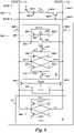
- Figures 3A and 3Bare block diagrams of logic/memory devices 305 and 307 in accordance with a number of embodiments of the present disclosure.
- the logic/memory device embodiments 305 and 307illustrate logic partitioned (also referred to as "partitioned logic") between a memory component 301 and a logic component 302.
- the logic/memory device embodiments 305 and 307may be a part of a 3D logic/memory device stack as shown in Figure 4 and may include I/O channels 355 coupling the memory components 301 to the logic components 302.
- the I/O channelsmay be in the form of through silicon vias (TSVs).
- TSVsmay be formed either entirely or partially through silicon or other single, composite and/or doped substrate material to the components.
- TSV technologyallows for additional signaling between a logic component 302 and one or more memory components 301.
- PIM capable device controller operationlike that shown as 240 in Figure 2 , can be partitioned between a logic component 302 and memory components 301 of a 3D logic/memory device stack.
- control logic 331(representing the control logic structure and functions described in connection with 231 in Figure 2 ) may be located on the logic component 302 to enhance and facilitate close integration with the processing resources of one or more hosts such as hosts 510 discussed in Figures 5A and 5B in a distributed computing system and/or in system on chip (SoC) environment.
- hosts 510discussed in Figures 5A and 5B in a distributed computing system and/or in system on chip (SoC) environment.
- SoCsystem on chip
- Figure 2provided a PIM device 220 example in which the controller 240 was described having three parts; control logic, sequencer and timing circuitry.
- the timing circuitry 233 and the sequencer 232were described as relatively small state machines and the control logic 231 was described as being a microcoded engine.
- Figure 3Aillustrates an example logic/memory device 305 embodiment in which both the control logic 331 and the sequencer 332 are located on the logic component 302 of the logic/memory device 305, but still coupled to the one or more memory components 301 via high speed I/O channel 355.
- the control logic 331may be in the form of a microcoded engine such as an embedded, reduced instruction set computer (RISC) type controller and the sequencer 332 may be in the form of a state machine.
- RISCreduced instruction set computer
- both the control logic 331 and the sequencer 332may be in the form of microcoded engines.
- an engineis intended to include hardware and may include software and/or firmware, but at least includes hardware, e.g., circuitry in the form of an application specific integrated circuit (ASIC).
- ASICapplication specific integrated circuit
- microcodemay be used and executed on the PIM device by a reduced instruction set computer (RISC) type controller, ASIC, etc.
- RISC type controlleris one of a family of processors which operates on a reduced bit length instruction, e.g., a 32 or 64 bit length instruction.
- reference to microcode instructions on a PIM capable deviceis intended to include a 32 or 64 bit length instruction.
- embodimentsmay include other bit length instructions.
- execution of microcode instructions for PIM capable logic/memory devices 305 and 307is performed by logic component 302, separate from a host 110 as shown in Figure 1 and also separate from the memory component 301.
- the timing circuitry 333is remains with the memory component 301.
- the timing circuitry 333 on the memory component 301may be referred to as "first partitioned logic”.
- the timing circuitry 333can represent the timing circuitry 233 describe with the PIM capable device 220 in Figure 2 .
- the control logic 331 and the sequencer 332may be configured to execute particularly developed firmware, e.g., particular purpose PIM microcode, on the logic component 302.
- the embodiment of Figure 3Billustrates an embodiment of the present disclosure in which the control logic 331 is located on the logic component 302 of the logic/memory device 307, but both the sequencer 332 and the timing circuity 333 remain on the memory component 301.
- the sequencer 332 and the timing circuitry 333may be referred to as the "first partitioned logic" as being located on the memory component 301.
- the control logic 331is still coupled to the memory component 301 via high speed I/O channel 355.
- the sequencer 332 and timing circuitry 333may represent timing circuitry 233 and sequencer 232 as described in connection with Figure 2 .
- the timing circuitry 333 and sequencer 332 on the memory component 301may both be state machines to provide timing and control command sequencing, respectively.
- the timing circuitry 333 and sequencer 332may be compact yet be responsible for providing conflict free access to arrays, e.g., DRAM arrays, and/or sensing circuitry, such as array 130 and sensing circuitry 150 in Figure 1 , for logical operations performed on a bank 321.
- the sequencer 332 and timing circuitry 333are separate from the control registers 136 used in normal DRAM logical operations such as read, write, copy, and/or move DRAM array operations.
- the memory component 301 of the logic/memory devices 305 and 307may contain one or more banks 321.
- the banks 321may contain an array of memory cells 330 and sensing circuitry 350 coupled thereto.
- the array 330 and sensing circuitry 350may represent array 130 and sensing circuitry 150 described in connection with Figure 1 .
- Embodiments of the sensing circuitry 350are described in more detail in connection with Figures 6-8 .
- the memory component 301 of the logic/memory devices 305 and 307may include additional circuitry in the form of I/O buffers and/or extend row address (XRA) registers, row address strobe (RAS) logic, etc. 370.
- This additional logic circuitry 370may represent addition logic circuitry 170 described in Figure 1 .
- the logic component 302can include switching circuitry 323 to provide routing across arrays 330 associated with one or more banks 321.
- the switching circuitry 330may replace or perform at least some of the functions of the HSI 241 described in connection with Figure 2 .
- placing at least the control logic 331 on the logic component 302 of the logic/memory devices 305 and 307may allow for higher speed device operation by facilitating tight integration to a host processing resource such as host 110 shown in Figure 1 and/or host device(s) 510 shown and described in connection with Figures 5A and 5B .
- the control logic 331 on the logic component 302may be referred to as "second partitioned logic”.
- the control logic and the sequencer 332may collectively be referred to as the "second partitioned logic" as being located on the logic component 302.
- coordinated caching on the logic component 302 with the one or more memory components 301 of the logic/memory devices 305 and 307may be achieved.
- improved integration with existing cache coherency protocols to separate hostssuch as host 110 in Figure 1 and/or host device(s) shown in Figures 5A and 5B , may be achieved both closely as part of control logic 331 and/or more loosely with switching circuitry 323 and I/Os 355 (e.g., such as exists with a client on a symmetric multiprocessing (SMP)-capable bus).
- SMPsymmetric multiprocessing
- the example embodiments shown in Figures 3A and 3Bcan facilitate direct memory access (DMA) functionality both inter-bank and intra-bank to one or more banks 321.
- DMAdirect memory access
- the logic/memory device embodiments 305 and 307may allow for a lower latency to be achieved with PIM command routing operations. The same may be achieved even with the timing circuitry 333 of the memory component 301 operating in a different clock domain and/or at a different clock speed than a clock domain and/or clock speed of the control logic 331 on the logic component 302.
- the logic component 302can include arbitration circuitry 339.
- the arbitration circuitryis configured to apply a scheduling policy that prioritizes between normal DRAM requests and PIM requests, e.g., PIM commands, for use of array 300 that are received at the logic component 302 by the switching circuitry 323 and/or control logic 331.
- the arbitration circuitry 339may be formed as an integrated circuit with the control logic 331 and sequencer 332 to collectively form logic 325 on the logic component 302 of logic/memory device 305.
- the logic 325may represent the partitioned logic 525 on the logic component 502 of a logic/memory device 520 shown and described in the embodiment of Figure 5A .
- the arbitration circuitry 339may be formed as an integrated circuit with the control logic 331 to collectively form logic 325 on the logic component 302 of logic/memory device 307.
- the logic 325may represent the partitioned logic 525 on the logic component 502 of a logic/memory device 520 shown and described in the embodiment of Figure 5B .
- the scheduling policies implemented by the arbitration circuitrymay be according to an all, some, or none set of rules for prioritizing between DRAM requests and PIM requests received at a logic component 302 for use of an array 330 and/or sensing circuitry 350 of a bank 321 on a memory component 301.
- one policymay allow a DRAM request received at the logic component 302 to always halt, e.g., stop or pause, a PIM command operation associated with an earlier PIM request.
- the arbitration circuitry 339may be configured to detect whether a threshold number or type of DRAM requests are received at the logic component 302 within a particular time window, e.g., within a particular number of packet frames, clock cycles, etc., after a PIM request is received at the logic component 302. In such an example policy, if a threshold number or type of DRAM requests are received at the logic component 302 within the particular time window, then the arbitration circuitry 339 may be configured to stop or hold PIM command request execution associated with an earlier PIM request until after performance of the DRAM request later received at the logic component 302. Alternatively, in another example policy the arbitration circuitry 339 may be configured to give priority to certain or all PIM requests received at the logic component 302 over certain or all DRAM requests received at the logic component 302. Embodiments are not limited to these examples.
- the apparatus and methods described hereinprovide embodiments that are not constrained to the control of normal control registers, e.g., double data rate (DDR) timing control registers, associated with memory arrays, e.g., DRAM arrays.
- DDRdouble data rate
- the timing circuitry 333 in the memory component 301is configured for logical operations on PIM capable logic/memory devices 305 and 307 separate from the normal control registers shown as 136 in Figure 1 .
- control logic 331 and the sequencer 332may be variously located between the logic component 302 and the memory component 301 to achieve PIM capable logic/memory devices 305 and 307 which can perform logical operations described in more detail in connection with Figures 6-8 .
- the partitioned logic 325can, in at least one embodiment, maintain cache coherency between the logic component 302 and the memory component 301.
- the partitioned logic 325may be configured to create a block select as metadata to a cache line and to create a subrow select as metadata to the cache line.
- the partitioned logic 325may be in the form of hardware, software and/or firmware, but at least hardware in the form of circuitry to execute instructions and/or perform logical operations.
- the partitioned logic 325is configured to create and use the block select metadata to enable an offset to a cache line associated with a separate host.
- the partitioned logic 325is further configured to create and use the subrow select to enable multiple sets to set associative cache used by a separate host.
- the block selectmay provide an offset to a page in a dynamic random access memory (DRAM).
- the partitioned logic 325 of the logic component 302 that is coupled to the memory component 301may be configured to generate a bulk invalidate command to a cache memory upon receipt of a bit vector operation instruction.
- bit vectoris intended to mean a physically contiguous number of bits on a bit vector memory device, e.g., PIM device, whether physically contiguous in rows (e.g., horizontally oriented) or columns (e.g., vertically oriented) in an array of memory cells.
- bit vector operationis intended to mean an operation that is performed on a bit-vector that is a contiguous portion (also referred to as "chunk") of virtual address space, e.g., used by a PIM device.
- a chunk of virtual address spacemay have a bit length of 256 bits.
- a chunkmay or may not be contiguous physically to other chunks in the virtual address space.
- the term "bulk”is intended to mean a capability to address and operate on information in multiple locations, e.g., multiple cache lines, without having to separately address and communicate instructions to each of the multiple locations.
- the cache architectureuses part of an address generated by a processor associated with a host to locate the placement of a block in the cache and may have some metadata (e.g., valid and dirty bits) describing the state of the cache block. This is because processing resources should have the same view of memory. Accordingly, a cache based memory system will use some form of cache coherency protocol, e.g., either a MESI (modified, exclusive, shared, invalid) or directory based cache coherency protocol, to maintain access to accurate data in the cache memory system between processing resources.
- MESImodified, exclusive, shared, invalid
- a last level cache architecturemay be constructed for intended use with a 3D integrated memory, with tags and meta data being stored on-chip in SRAM and the block data being stored in quickly accessed DRAM.
- the matchingoccurs using the on-chip SRAM tags and the memory access is accelerated by the relatively fast on-package DRAM (as compared to an off-package solution).
- microcode instructions executing on a processing resourcemay want to access an array of the PIM capable device to perform a bit vector based operation.
- a processing resource associated with a hostmay only be aware of the host's cache line bit length for use in maintaining cache coherency on the host.
- a bit vector based operation in a PIM capable devicemay operate on bit vectors of a much different bit length.
- a typical use pattern for performing a bit vector based operation and maintaining cache coherency in softwaremay involve expensive flushing of an entire cache or marking particular pages as "uncacheable".
- To make a PIM capable device cache coherency protocol aware to a level equivalent to that of a hostwould be very costly and complex in terms of hardware and software device space usage and design development time. Further, even if this were done for a cache coherency protocol of a particular host platform, the PIM capable device would not be cache coherency protocol aware for hosts of different platforms using different cache coherency protocols.
- the partitioned logic 325can include hardware, e.g., in the form of an application specific integrated circuit (ASIC), configured to and can operate on more compactly designed microcode instructions in the form of firmware, e.g., 32 or 64 bit microcode instructions stored in array 330 and executed by the control logic 331.
- the partitioned logic 325may include an invalidate engine (not shown) associated with the control logic 331.
- control logic 331may be configured for a particular cache coherency protocol associated with a host's cache memory using particularly designed firmware to implement particular PIM operations at a significantly lower costs that that which would be required by hardware and software which fully replicated a host cache coherency protocol.
- control logic 331 in the partitioned logic 325may be configured to recognize the above described block select and the subrow select metadata and use that metadata to provide a compute enabled cache.
- memory banks 321 on the memory component 301may have independent I/O paths, e.g., TSVs, coupling to the control logic 331 of the logic component 302 and may be controlled explicitly by the partitioned logic 325 on the logic component 302.
- cache blocks on a logic component 302may be moved from an SRAM in the logic component 302 into a DRAM array in a bank 321 on the memory component 301.
- the placement of the cache blocksmay be controlled using the metadata data structures created and added to the host cache lines by the control logic 331 of the partitioned logic 325 on the logic component 302.
- the block select and subrow select metadata data structuresmay be data structures internal to the logic/memory device embodiments 305 and 307, e.g., stored and maintained between the logic component 302 and memory component 301 and not stored, maintained or tracked as part of an address to the processing resources on a host, e.g., host 110 in Figure 1 .
- control logic 331 on the partitioned logic 325 on the logic component 302is at least hardware configured to execute microcoded instructions. In this manner, the control logic 331 may be configured to change the block select and the subrow select, as needed, and be configured to relocate the cache block data transparently to the processing resources of a host.
- the control logic 325can additionally be configured to store and maintain a copy of the block select and subrow select metadata structures with processing resources of a separate host. Embodiments are not limited to the example given herein.
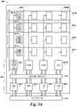
- Figure 4illustrates an example of a system on a chip (SoC) 400 having a plurality of adjacent and coupled memory components 401-1, 401-2, .. ., 401-N (referred to collectively as 401) which are further coupled to a logic component 402.
- the plurality of adj acent and coupled memory components 401-1, ..., 401-Nmay be in the form of a plurality of individual memory die and/or distinct memory layers formed as integrated circuits on a chip.
- the plurality of memory components 401can further be partitioned into distinct portions 421 of the plurality of memory components 401, e.g., partitioned into separate and distinct dynamic random access memory (DRAM) banks on each memory component 401.
- DRAMdynamic random access memory
- the logic component 402may be in the form of an individual logic die and/or distinct logic layers formed as integrated circuits on a chip.
- the SoC 400provides three dimensions (3D) by stacking the plurality of memory components 401 and interconnecting at least one memory component 401-1, ..., 401-N and to a logic component 402 to collectively form a logic/memory device 420.
- the plurality of memory components 401-1, . . ., 401-Ncan be coupled to the logic component 402 using I/O paths, e.g., through silicon vias (TSVs) (not shown).
- TSVssilicon vias
- an apparatusis intended to mean one or more components, devices and/or systems which may be coupled to achieve a particular function.
- a systemas used herein, is intended to mean a collection of devices coupled together, whether in wired or wireless fashion, to form a larger network, e.g., as in a distributed computing network.
- a componentas used herein, is intended to mean a die, substrate, layer, and/or integrated circuitry.
- a devicemay be formed within or among components.
- a "device"such as a memory device may be wholly within a memory component.
- a devicesuch as a logic/memory device is intended to mean some combination of logic and memory components.
- a memory device, logic device, and/or logic/memory deviceall include devices able to perform a logical operation, e.g., an apparatus able to perform a Boolean logical operation.
- TSV manufacturing techniquesenable interconnection of multiple die layers in order to construct three-dimensional dies. This ability to interconnect multiple die layers permits building a memory device with a combination of memory storage layers and one or more logic layers. In this manner, the device provides the physical memory storage and logical memory transaction processing in a single electronic device package.
- the arrangement shown in Figure 4is to illustrate an example configuration. Embodiments described herein, however, are not limited to this example and/or a particular die/layer arrangement.
- the SoC 400 example shown in Figure 4may provide a very compact and power efficient package with available bandwidth capacity of 320GB/s per device.
- the illustrated SoC 400may be capable of high bandwidth via a hierarchical and parallel approach to the design.
- a device hierarchymay occur across the logic and memory components and hardware parallelism may occur in a planar manner across a given component.
- a combination and/or organization of logic and memory resources between the plurality of memory components 401-1, ..., 401-N and one or more logic components 402 for the SoC 400may be referred to as a logic/memory device 420.
- Through-silicon vias (TSVs)may interconnect each of the memory components 401-1, ..., 401-N and one or more logic components 402, e.g., die and/or layers for each logic/memory device 420.
- TSVsThrough-silicon vias
- the SoC 400is shown organized into sixteen (16) logic/memory devices 420 with each device associated with at least a portion of the logic component 402 and a portion of one or more of the plurality of memory components 401-1, . . ., 401-N.
- Embodiments, however,are not limited to this example. Embodiments can include geometric and/or numerical configurations different from that described and illustrated in Figure 4 .
- Figure 5Ais a block diagram illustrating in two-dimensions an embodiment of a quadrant 509 of SoC 400 shown in Figure 4 .
- Figure 5Bis a block diagram illustrating in two-dimensions another embodiment of a quadrant 511 of SoC 400 shown in Figure 4 .
- four logic/memory devices 520-1, ..., 520-Mare shown (each logic/memory device generally referred to as 520) with each logic/memory device 520 including a partitioned portion 521-1, ..., 521-N (e.g., particular memory banks) of the plurality of adjacent and coupled memory components 501-1,. .
- At least one logic component 502is adjacent to and coupled to the plurality of memory components 501-1, . . ., 501-N.
- each logic/memory device 520may include separate logic 525-1, . .., 525-M (also referred to as “partitioned logic” or “second partitioned logic” in relation to location on the logic component 502) which is a partitioned portion of the logic component 502 relative to a particular logic/memory device 520-1, ..., 520-M.
- each partitioned logic 525-1, ..., 525-M(generally referred to as 525) includes control logic 531 and sequencer 532 to form a PIM capable logic/memory device 520 with timing circuitry 533 in the partitioned portions 521-1, ..., 521-N of the plurality of memory components 501-1, ..., 501-N.
- Control logic 531 and sequencer 532may represent the control logic 231/331 and sequencer 232/332 shown in Figures 2 , 3A and 3B .
- Timing circuitry 533is shown separate and distinct from the normal control registers and timing circuitry 536, e.g., DDR control registers and timing circuitry, which may be used for the partitioned portions 521-1, ..., 521-N of the plurality of memory components 501-1, ..., 501-N.
- the timing circuitry 533may represent the timing circuitry 233/333 shown in Figures 2 , 3A and 3B and the normal control registers and timing circuitry 536 may represent the registers 136 shown in Figure 1 .
- partitioned logic 525may manage memory reference operations for a logic/memory device 520.
- partitioned logic 525may provide access to one or more partitioned portions 521-1, ..., 521-M (e.g., particular memory banks) of the plurality of memory components 501-1, ..., 501-N.
- the partitioned portions 521-1, ..., 521-N of the plurality of memory components 501-1, ..., 501-Nmay permit memory transactions to exist in parallel not only across partitioned portions 521-1, ..., 521-N of the memory components 501-1, ..., 501-N within a target logic/memory device 520-1, but also in parallel across logic/memory devices 520-1, ..., 520-M.
- the partitioned logic 525-1, ..., 525-M of a logic component 502may be in the form of control logic, state machine, etc..
- the partitioned logic 525-1, ..., 525-Mmay be in the form of hardware and firmware to implement functions described herein.
- the partitioned logic, 525-1, ..., 525-M of a logic component 502includes at least control logic 531 (shown as 331 in Figures 3A and 3B ).
- a sequencer 532shown as 332 in Figure 3A ) for each logic/memory device 520 is also included on the logic component 502 to form a processing in memory (PIM) capable logic/memory device 520.
- PIMprocessing in memory
- a sequencer 532(shown as 332 in Figure 3B ) for each logic/memory device 520 is provided on each portion 521-1, ..., 521-N of the plurality of memory components 501-1, . . ., 501-N to form a PIM capable logic/memory device 520.
- the control logic 531may be in the form of a microcoded engine which can execute microcode instructions.
- an engineis intended to mean hardware and/or software, but at least hardware in the form of transistor circuitry and/or an application specific integrated circuit (ASIC).
- the sequencer 532may also be in the form of a microcoded engine.
- the logic component 502may include external input/output (I/O) link access, e.g., links 529-1, ..., 529-4, to the logic/memory devices 520 as well as internal switching circuitry 523.
- the external I/O linkse.g., links 529-1, . . ., 529-4 (generally referred to as 529), may be provided by four, eight, or more logical links.
- four links 529-1, ..., 529-4(Link 0, Link 1, Link 2, and Link 3) are shown coupled to switching circuitry 523.
- the switching circuitry 523may direct transactions among a plurality of logic/memory devices 520, e.g., to partitioned logic 525-1, ..., 525-M associated with the portions 521-1, ..., 521-N of the plurality of memory components 501-1, . . ., 501-N.
- the links 529may support the ability to couple logic/memory devices 520 to both hosts 510 or other network devices. This coupling can facilitate the construction of memory subsystems with capacities larger than a single logic/memory device 520 while not perturbing native link structures and packetized transaction protocols.
- Links 529can be configured as host device links or pass-through links in a multitude of topologies. In example, four potential device topologies based upon the example four-link configuration can be configured in a network topology. These four potential device topologies include mesh, torus and/or crossbar topologies. Chaining multiple logic/memory devices 520 together can increase a total memory capacity available to a host 510.
- the partitioned logic 525 of the logic component 502 for a device 520may include direct inline memory module (DIMM) control logic 531 for each independent device 520.
- DIMMdirect inline memory module
- four partitioned logic setsare shown, e.g., 525-1, ..., 525-M, each associated with a particular device 520.
- Each partitioned logic 525-1, ..., 525-Mmay be loosely associated with a link 529-1, ..., 529-4.
- one or more host(s) 510may have the ability to minimize bandwidth latency through the logic component 502 by logically sending request packets to links 529 physically closest to the associated partitioned logic 525 of a particular device 520.
- partitioned portions 521-1, 521-2, . .., 521-N(generally referred to as 521) of the plurality of memory components 501-1, ..., 501-N within a target device 520 may be broken into banks of dynamic random access memories (DRAMs).
- DRAMsdynamic random access memories
- access through stacked memory components 501-1, ..., 501-Nmay access a particular memory bank, e.g., DRAM bank.
- ., 501-Nare separate die and/or distinct memory layers, lower banks, e.g., 521-1, can be configured in lower die and/or layers, e.g., 501-1, while higher banks, e.g., 521-2, ..., 521-N, can be configured in higher die and/or layers, e.g., 501-2, ..., 501-N.
- a DRAM bankmay be organized using rows and columns with 16K columns and 512 rows.
- partitioned logic 525-1, ..., 525-Mmay organize DRAM into one megabit (1Mb) blocks each addressing 16-bytes. Read or write requests to a partitioned portions 521-1, ..., 521-N of the plurality of memory components 501-1, ..., 501-N can be performed in 32-bytes for each column fetch.
- partitioned logic 525including control logic 531 associated with a plurality of banks 521-1, ..., 521-N for a given logic/memory device 520 can decode signals received from a host 510.
- these signalscan include chip enable signals, write enable signals, debugging indication signals, and address latch signals that are used to control DRAM bank operations, including traditional data read, data write, and data erase operations as well as logical Boolean AND, OR, XOR, etc. operations performed with the memory arrays and/or sensing circuitry to a PIM capable DRAM bank.
- partitioned logic 525may be responsible for executing instructions from a host 510 for a PIM capable logic/memory device 520.
- the partitioned logic 525 of the logic component 502includes control logic 531 and a sequencer 532 and the partitioned portions 521-1, ..., 521-N of the plurality of memory components 501-1, ..., 501-N include timing circuitry 533, separate from traditional DDR control registers 536, associated with a PIM capable logic/memory device 520 to perform logical operations.
- the partitioned logic 525 of the logic component 502includes control logic 531 and the partitioned portions 521-1, ..., 521-N of the plurality of memory components 501-1, ..., 501-N include a sequencer 532 and timing circuitry 533, separate from traditional DDR control registers 536, associated with a PIM capable logic/memory device 520 to perform logical operations.
- the logic/memory devices described in Figures 3A-5Bmay be configured to execute of PIM commands to control sensing circuitry including compute components shown as 631 in Figure 6 and 731 in Figure 7 , to implement logical functions such as AND, OR, NOT, NAND, NOR, and XOR logical functions. Additionally the logic/memory devices described in Figures 3A-5B may be configured to control the sensing circuitry to perform non-Boolean logic operations, including copy, compare and erase operations, as part of executing DRAM requests. Thus, one or more logical functions of the controller 240 to a PIM capable device described in connection with Figure 2 may be partitioned between a plurality of memory components and one or more logic components to a logic/memory device.
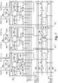
- FIG. 6is a schematic diagram illustrating sensing circuitry 650 in accordance with a number of embodiments of the present disclosure.
- the sensing circuitry 650can represent the sensing circuitry 150 shown in Figure 1 .
- a memory cellcomprises a storage element (e.g., capacitor) and an access device (e.g., transistor).
- a first memory cellcomprises transistor 602-1 and capacitor 603-1
- a second memory cellcomprises transistor 602-2 and capacitor 603-2, etc.
- the memory array 630is a DRAM array of 1T1C (one transistor one capacitor) memory cells.
- the memory cellsmay be destructive read memory cells (e.g., reading the data stored in the cell destroys the data such that the data originally stored in the cell is refreshed after being read).
- the cells of the memory array 630can be arranged in rows coupled by word lines 604-X (Row X), 604-Y (Row Y), etc., and columns coupled by pairs of complementary sense lines (e.g., data lines DIGIT(n-1)/DIGIT(n-1)_, DIGIT(n)/DIGIT(n)_, DIGIT(n+1)/DIGIT(n+1)_).
- the individual sense lines corresponding to each pair of complementary sense linescan also be referred to as data lines 605-1 (D) and 605-2 (D_) respectively.
- an array of memory cellscan include additional columns of memory cells and/or data lines (e.g., 4,096, 8,192, 16,384 data lines, etc.).
- Memory cellscan be coupled to different data lines and/or word lines.
- a first source/drain region of a transistor 602-1can be coupled to data line 605-1 (D)
- a second source/drain region of transistor 602-1can be coupled to capacitor 603-1
- a gate of a transistor 602-1can be coupled to word line 604-Y.
- a first source/drain region of a transistor 602-2can be coupled to data line 605-2 (D_)
- a second source/drain region of transistor 602-2can be coupled to capacitor 603-2
- a gate of a transistor 602-2can be coupled to word line 604-X.
- the cell plateas shown in Figure 6 , can be coupled to each of capacitors 603-1 and 603-2.
- the cell platecan be a common node to which a reference voltage (e.g., ground) can be applied in various memory array configurations.
- the memory array 630is coupled to sensing circuitry 650 in accordance with a number of embodiments of the present disclosure.
- the sensing circuitry 650comprises a sense amplifier 606 and a compute component 631 corresponding to respective columns of memory cells (e.g., coupled to respective pairs of complementary data lines).
- the sense amplifier 606can be coupled to the pair of complementary sense lines 605-1 and 605-2.
- the compute component 631can be coupled to the sense amplifier 606 via pass gates 607-1 and 607-2.
- the gates of the pass gates 607-1 and 607-2can be coupled to logical operation selection logic 613.
- the logical operation selection logic 613can be configured to include pass gate logic for controlling pass gates that couple the pair of complementary sense lines un-transposed between the sense amplifier 606 and the compute component 631 and/or swap gate logic for controlling swap gates that couple the pair of complementary sense lines transposed between the sense amplifier 606 and the compute component 631.
- the logical operation selection logic 613can also be coupled to the pair of complementary sense lines 605-1 and 605-2.
- the logical operation selection logic 613can be configured to control continuity of pass gates 607-1 and 607-2 based on a selected logical operation, as described in detail below for various configurations of the logical operation selection logic 613.
- the sense amplifier 606can be operated to determine a data value (e.g., logic state) stored in a selected memory cell.
- the sense amplifier 606can comprise a cross coupled latch, which can be referred to herein as a primary latch.
- the circuitry corresponding to sense amplifier 606comprises a latch 615 including four transistors coupled to a pair of complementary data lines D 605-1 and D_ 605-2.
- embodimentsare not limited to this example.
- the latch 615can be a cross coupled latch (e.g., gates of a pair of transistors, such as n-channel transistors (e.g., NMOS transistors) 627-1 and 627-2 are cross coupled with the gates of another pair of transistors, such as p-channel transistors (e.g., PMOS transistors) 629-1 and 629-2).
- the cross coupled latch 615 comprising transistors 627-1, 627-2, 629-1, and 629-2can be referred to as a primary latch.
- the voltage on one of the data lines 605-1 (D) or 605-2 (D_)will be slightly greater than the voltage on the other one of data lines 605-1 (D) or 605-2 (D_).
- An ACT signal and the RNL ⁇ signalcan be driven low to enable (e.g., fire) the sense amplifier 606.
- the data lines 605-1 (D) or 605-2 (D_) having the lower voltagewill turn on one of the PMOS transistor 629-1 or 629-2 to a greater extent than the other of PMOS transistor 629-1 or 629-2, thereby driving high the data line 605-1 (D) or 605-2 (D_) having the higher voltage to a greater extent than the other data line 605-1 (D) or 605-2 (D_) is driven high.
- the data line 605-1 (D) or 605-2 (D_) having the higher voltagewill turn on one of the NMOS transistor 627-1 or 627-2 to a greater extent than the other of the NMOS transistor 627-1 or 627-2, thereby driving low the data line 605-1 (D) or 605-2 (D_) having the lower voltage to a greater extent than the other data line 605-1 (D) or 605-2 (D_) is driven low.
- the data line 605-1 (D) or 605-2 (D_) having the slightly greater voltageis driven to the voltage of the supply voltage V CC through source transistor 611, and the other data line 605-1 (D) or 605-2 (D_) is driven to the voltage of the reference voltage (e.g., ground) through the sink transistor 613. Therefore, the cross coupled NMOS transistors 627-1 and 627-2 and PMOS transistors 629-1 and 629-2 serve as a sense amplifier pair, which amplify the differential voltage on the data lines 605-1 (D) and 605-2 (D_) and operate to latch a data value sensed from the selected memory cell.
- Embodimentsare not limited to the sense amplifier 606 configuration illustrated in Figure 6 .
- the sense amplifier 606can be current-mode sense amplifier and/or single-ended sense amplifier (e.g., sense amplifier coupled to one data line).
- embodiments of the present disclosureare not limited to a folded data line architecture such as that shown in Figure 6 .
- the sense amplifier 606can, in conjunction with the compute component 631, be operated to perform various logical operations using data from an array as input.
- the result of a logical operationcan be stored back to the array without transferring the data via a data line address access (e.g., without firing a column decode signal such that data is transferred to circuitry external from the array and sensing circuitry via local I/O lines).
- a number of embodiments of the present disclosurecan enable performing logical operations and compute functions associated therewith using less power than various previous approaches.
- a number of embodimentscan enable an increased parallel processing capability as compared to previous approaches.
- the sense amplifier 606can further include equilibration circuitry 614, which can be configured to equilibrate the data lines 605-1 (D) and 605-2 (D_).
- the equilibration circuitry 614comprises a transistor 624 coupled between data lines 605-1 (D) and 605-2 (D_).
- the equilibration circuitry 614also comprises transistors 625-1 and 625-2 each having a first source/drain region coupled to an equilibration voltage (e.g., V DD /2), where V DD is a supply voltage associated with the array.
- a second source/drain region of transistor 625-1can be coupled data line 605-1 (D), and a second source/drain region of transistor 625-2 can be coupled data line 605-2 (D_).
- Gates of transistors 624, 625-1, and 625-2can be coupled together, and to an equilibration (EQ) control signal line 626.
- EQequilibration
- activating EQenables the transistors 624, 625-1, and 625-2, which effectively shorts data lines 605-1 (D) and 605-2 (D_) together and to the an equilibration voltage (e.g., V DD /2).
- Figure 6shows sense amplifier 606 comprising the equilibration circuitry 614
- the equilibration circuitry 614may be implemented discretely from the sense amplifier 606, implemented in a different configuration than that shown in Figure 6 , or not implemented at all.
- the sensing circuitrye.g., sense amplifier 606 and compute component 631
- the sensing circuitrycan be operated to perform a selected logical operation and initially store the result in one of the sense amplifier 606 or the compute component 631 without transferring data from the sensing circuitry via an I/O line (e.g., without performing a data line address access via activation of a column decode signal).
- Boolean logic functionsare used in many higher level functions. Consequently, speed and/or power efficiencies that can be realized with improved logical operations, can translate into speed and/or power efficiencies of higher order functionalities.
- the compute component 631can also comprise a latch, which can be referred to herein as a secondary latch 664.
- the secondary latch 664can be configured and operated in a manner similar to that described above with respect to the primary latch 615, with the exception that the pair of cross coupled p-channel transistors (e.g., PMOS transistors) of the secondary latch can have their respective sources coupled to a supply voltage (e.g., V DD ), and the pair of cross coupled n-channel transistors (e.g., NMOS transistors) of the secondary latch can have their respective sources selectively coupled to a reference voltage (e.g., ground), such that the secondary latch is continuously enabled.
- a reference voltagee.g., ground
- Figure 7is a schematic diagram illustrating sensing circuitry capable of implementing an XOR logical operation in accordance with a number of embodiments of the present disclosure.
- Figure 7shows a sense amplifier 706 coupled to a pair of complementary sense lines 705-1 and 705-2, logical operation select logic 713, and a compute component 731 coupled to the sense amplifier 706 via pass gates 707-1 and 707-2.
- the sense amplifier 706 shown in Figure 7can correspond to sense amplifier 606 shown in Figure 6 .
- the compute component 731 shown in Figure 7can correspond to sensing circuitry, including compute component, 150 in Figure 1 .
- the logical operation selection logic 713 shown in Figure 7can correspond to logical operation selection logic 613 shown in Figure 6 .
- the gates of the pass gates 707-1 and 707-2can be controlled by a logical operation selection logic 713 signal, (e.g., Pass).
- a logical operation selection logic 713 signale.g., Pass
- an output of the logical operation selection logic 713can be coupled to the gates of the pass gates 707-1 and 707-2.
- the compute component 731can comprise a loadable shift register configured to shift data values left and right.
- the compute components 731can comprise respective stages (e.g., shift cells) of a loadable shift register configured to shift data values left and right.
- each compute component 731 (e.g., stage) of the shift registercomprises a pair of right-shift transistors 781 and 786, a pair of left-shift transistors 789 and 790, and a pair of inverters 787 and 788.
- the signals PHASE 1R, PHASE 2R, PHASE 1L, and PHASE 2Lcan be applied to respective control lines 782, 783, 791 and 792 to enable/disable feedback on the latches of the corresponding compute components 731 in association with performing logical operations and/or shifting data in accordance with embodiments described herein.
- the sensing circuitry shown in Figure 7shows operation selection logic 713 coupled to a number of logic selection control input control lines, including ISO, TF, TT, FT, and FF. Selection of a logical operation from a plurality of logical operations is determined from the condition of logic selection control signals on the logic selection control input lines, as well as the data values present on the pair of complementary sense lines 705-1 and 705-2 when isolation transistors 750-1 and 750-2 are enabled via an ISO control signal being asserted.
- logic selection control input control linesincluding ISO, TF, TT, FT, and FF.
- the operation selection logic 713can include four logic selection transistors: logic selection transistor 762 coupled between the gates of the swap transistors 742 and a TF signal control line, logic selection transistor 752 coupled between the gates of the pass gates 707-1 and 707-2 and a TT signal control line, logic selection transistor 754 coupled between the gates of the pass gates 707-1 and 707-2 and a FT signal control line, and logic selection transistor 764 coupled between the gates of the swap transistors 742 and a FF signal control line.
- Gates of logic selection transistors 762 and 752are coupled to the true sense line through isolation transistor 750-1 (having a gate coupled to an ISO signal control line).
- Gates of logic selection transistors 764 and 754are coupled to the complementary sense line through isolation transistor 750-2 (also having a gate coupled to an ISO signal control line).
- Data values present on the pair of complementary sense lines 705-1 and 705-2can be loaded into the compute component 731 via the pass gates 707-1 and 707-2.
- the compute component 731can comprise a loadable shift register.
- the pass gates 707-1 and 707-2are OPEN, data values on the pair of complementary sense lines 705-1 and 705-2 are passed to the compute component 731 and thereby loaded into the loadable shift register.
- the data values on the pair of complementary sense lines 705-1 and 705-2can be the data value stored in the sense amplifier 706 when the sense amplifier is fired.
- the logical operation selection logic signal, Passis high to OPEN the pass gates 707-1 and 707-2.
- the ISO, TF, TT, FT, and FF control signalscan operate to select a logical function to implement based on the data value ("B") in the sense amplifier 706 and the data value ("A") in the compute component 731.
- the ISO, TF, TT, FT, and FF control signalsare configured to select the logical function to implement independent from the data value present on the pair of complementary sense lines 705-1 and 705-2 (although the result of the implemented logical operation can be dependent on the data value present on the pair of complementary sense lines 705-1 and 705-2.
- the ISO, TF, TT, FT, and FF control signalsselect the logical operation to implement directly since the data value present on the pair of complementary sense lines 705-1 and 705-2 is not passed through logic to operate the gates of the pass gates 707-1 and 707-2.
- Figure 7shows swap transistors 742 configured to swap the orientation of the pair of complementary sense lines 705-1 and 705-2 between the sense amplifier 706 and the compute component 731.
- the swap transistors 742are OPEN, data values on the pair of complementary sense lines 705-1 and 705-2 on the sense amplifier 706 side of the swap transistors 742 are oppositely-coupled to the pair of complementary sense lines 705-1 and 705-2 on the compute component 731 side of the swap transistors 742, and thereby loaded into the loadable shift register of the compute component 731.
- the logical operation selection logic 713 signal Passcan be activated (e.g., high) to OPEN the pass gates 707-1 and 707-2 (e.g., conducting) when the ISO control signal line is activated and either the TT control signal is activated (e.g., high) with data value on the true sense line is "1" or the FT control signal is activated (e.g., high) with the data value on the complement sense line is "1.”
- the data value on the true sense linebeing a "1" OPENs logic selection transistors 752 and 762.
- the data value on the complimentary sense linebeing a "1" OPENs logic selection transistors 754 and 764. If the ISO control signal or either the respective TT/FT control signal or the data value on the corresponding sense line (e.g., sense line to which the gate of the particular logic selection transistor is coupled) is not high, then the pass gates 707-1 and 707-2 will not be OPENed by a particular logic selection transistor.
- the logical operation selection logic signal Pass ⁇can be activated (e.g., high) to OPEN the swap transistors 742 (e.g., conducting) when the ISO control signal line is activated and either the TF control signal is activated (e.g., high) with data value on the true sense line is "1,” or the FF control signal is activated (e.g., high) with the data value on the complement sense line is "1.” If either the respective control signal or the data value on the corresponding sense line (e.g., sense line to which the gate of the particular logic selection transistor is coupled) is not high, then the swap transistors 742 will not be OPENed by a particular logic selection transistor.
- the Pass ⁇ control signalis not necessarily complementary to the Pass control signal. It is possible for the Pass and Pass ⁇ control signals to both be activated or both be deactivated at the same time. However, activation of both the Pass and Pass ⁇ control signals at the same time shorts the pair of complementary sense lines together, which may be a disruptive configuration to be avoided.
- the sensing circuitry illustrated in Figure 7is configured to select one of a plurality of logical operations to implement directly from the four logic selection control signals (e.g., logical operation selection is not dependent on the data value present on the pair of complementary sense lines). Some combinations of the logic selection control signals can cause both the pass gates 707-1 and 707-2 and swap transistors 742 to be OPEN at the same time, which shorts the pair of complementary sense lines 705-1 and 705-2 together.
- the logical operations which can be implemented by the sensing circuitry illustrated in Figure 7can be the logical operations summarized in the logic tables shown in Figure 8 .
- Figure 8is a logic table illustrating selectable logic operation results implemented by a sensing circuitry shown in Figure 7 in accordance with a number of embodiments of the present disclosure.
- the four logic selection control signalse.g., TF, TT, FT, and FF
- the four control signalsin conjunction with a particular data value present on the complementary sense lines, can be used to select one of plural logical operations to implement involving the starting data values stored in the sense amplifier 706 and compute component 731.
- the four control signalsin conjunction with a particular data value present on the complementary sense lines, controls the continuity of the pass gates 707-1 and 707-2 and swap transistors 742, which in turn affects the data value in the compute component 731 and/or sense amplifier 706 before/after firing.
- the capability to selectably control continuity of the swap transistors 742facilitates implementing logical operations involving inverse data values (e.g., inverse operands and/or inverse result), among others.
- Logic Table 8-1 illustrated in Figure 8shows the starting data value stored in the compute component 731 shown in column A at 844, and the starting data value stored in the sense amplifier 706 shown in column B at 845.
- the other 3 column headings in Logic Table 8-1refer to the continuity of the pass gates 707-1 and 707-2, and the swap transistors 742, which can respectively be controlled to be OPEN or CLOSED depending on the state of the four logic selection control signals (e.g., TF, TT, FT, and FF), in conjunction with a particular data value present on the pair of complementary sense lines 705-1 and 705-2.
- the "Not Open” columncorresponds to the pass gates 707-1 and 707-2 and the swap transistors 742 both being in a non-conducting condition
- the "Open True”corresponds to the pass gates 707-1 and 707-2 being in a conducting condition
- the "Open Invert”corresponds to the swap transistors 742 being in a conducting condition.
- the configuration corresponding to the pass gates 707-1 and 707-2 and the swap transistors 742 both being in a conducting conditionis not reflected in Logic Table 8-1 since this results in the sense lines being shorted together.
- the nine different selectable logical operations that can be implemented by the sensing circuitrye.g., 550 in Figure 5A
- Logic Table 8-2 illustrated in Figure 8including an XOR logical operation.
- the columns of Logic Table 8-2 illustrated in Figure 8show a heading 880 that includes the state of logic selection control signals.
- the state of a first logic selection control signalis provided in row 876
- the state of a second logic selection control signalis provided in row 877
- the state of a third logic selection control signalis provided in row 878
- the state of a fourth logic selection control signalis provided in row 879.
- the particular logical operation corresponding to the resultsis summarized in row 847.
- sensing circuitrysense amplifiers
- compute componentdynamic latches
- isolation devicesisolation devices
- shift circuitryshift circuitry
Landscapes
- Engineering & Computer Science (AREA)
- Microelectronics & Electronic Packaging (AREA)
- Computer Hardware Design (AREA)
- Dram (AREA)
- Computer Security & Cryptography (AREA)
- Signal Processing (AREA)
- Computer Networks & Wireless Communication (AREA)
- Computing Systems (AREA)
- Memory System (AREA)
- General Engineering & Computer Science (AREA)
- Physics & Mathematics (AREA)
- Algebra (AREA)
- General Physics & Mathematics (AREA)
- Mathematical Analysis (AREA)
- Mathematical Optimization (AREA)
- Mathematical Physics (AREA)
- Pure & Applied Mathematics (AREA)
- Theoretical Computer Science (AREA)
Description
- The present disclosure relates generally to semiconductor memory and methods, and more particularly, to apparatuses and methods for logic/memory devices.
- Memory devices are typically provided as internal, semiconductor, integrated circuits in computers or other computing systems. There are many different types of memory including volatile and non-volatile memory. Volatile memory can require power to maintain its data (e.g., host data, error data, etc.) and includes random access memory (RAM), dynamic random access memory (DRAM), static random access memory (SRAM), synchronous dynamic random access memory (SDRAM), and thyristor random access memory (TRAM), among others. Non-volatile memory can provide persistent data by retaining stored data when not powered and can include NAND flash memory, NOR flash memory, and resistance variable memory such as phase change random access memory (PCRAM), resistive random access memory (RRAM), and magnetoresistive random access memory (MRAM), such as spin torque transfer random access memory (STT RAM), among others.
- Computing systems often include a number of processing resources (e.g., one or more processors), which may retrieve and execute instructions and store the results of the executed instructions to a suitable location. A processing resource (e.g., CPU) can comprise a number of functional units such as arithmetic logic unit (ALU) circuitry, floating point unit (FPU) circuitry, and/or a combinatorial logic block, for example, which can be used to execute instructions by performing logical operations such as AND, OR, NOT, NAND, NOR, and XOR, and invert (e.g., inversion) logical operations on data (e.g., one or more operands). For example, functional unit circuitry may be used to perform arithmetic operations such as addition, subtraction, multiplication, and/or division on operands via a number of logical operations.
- A number of components in a computing system may be involved in providing instructions to the functional unit circuitry for execution. The instructions may be executed, for instance, by a processing resource such as a controller and/or host processor. Data (e.g., the operands on which the instructions will be executed) may be stored in a memory array that is accessible by the functional unit circuitry. The instructions and/or data may be retrieved from the memory array and sequenced and/or buffered before the functional unit circuitry begins to execute instructions on the data. Furthermore, as different types of operations may be executed in one or multiple clock cycles through the functional unit circuitry, intermediate results of the instructions and/or data may also be sequenced and/or buffered. A sequence to complete an operation in one or more clock cycles may be referred to as an operation cycle. Time consumed to complete an operation cycle costs in terms of processing and computing performance and power consumption, of a computing device and/or system.
- In many instances, the processing resources (e.g., processor and/or associated functional unit circuitry) may be external to the memory array, and data is accessed via a bus between the processing resources and the memory array to execute a set of instructions. Processing performance may be improved in a processor-in-memory (PIM) device, in which a processor may be implemented internal and/or near to a memory (e.g., directly on a same chip as the memory array). A PIM device may save time by reducing and/or eliminating external communications and may also conserve power. Document
US 2007/180006 discloses one example of an PIM device. In accordance with the present invention an apparatus, as set forth inclaim 1, is provided. Preferred embodiments of the invention are claimed in the dependent claims. Figure1 is a block diagram of an apparatus in the form of a computing system including one example of a processing in memory (PIM) capable device coupled to a host.Figure 2 is another block diagram in greater detail of a portion of one example of a PIM capable device.Figure 3A is a block diagram of a logic/memory device having logic shared between a memory component and a logic component in accordance with a number of embodiments of the present disclosure.Figure 3B is another block diagram of a logic/memory device having logic shared between a memory component and a logic component in accordance with a number of embodiments of the present disclosure.Figure 4 illustrates a representation of a computing system in accordance with a number of embodiments of the present disclosure.Figure 5A is a block diagram illustrating a quadrant of a computing system in accordance with a number of embodiments of the present disclosure.Figure 5B is another block diagram illustrating a quadrant of a computing system in accordance with a number of embodiments of the present disclosure.Figure 6 is a schematic diagram illustrating sensing circuitry to a memory device in accordance with a number of embodiments of the present disclosure.Figure 7 is a schematic diagram illustrating sensing circuitry to a memory device in accordance with a number of embodiments of the present disclosure.Figure 8 is a logic table illustrating selectable logic operation results implemented by a sensing circuitry shown inFigure 3 in accordance with a number of embodiments of the present disclosure.- The present disclosure includes apparatuses and methods for logic/memory device. In one example embodiment, execution of logical operations is performed on both one or more memory components and a logical component to a logic/memory device.
- An example apparatus comprises a plurality of memory components adjacent to and coupled to one another. A logic component is coupled to the plurality of memory components. At least one memory component comprises a partitioned portion having an array of memory cells and sensing circuitry coupled to the array. The sensing circuitry includes a sense amplifier and a compute component configured to perform operations. Timing circuitry is coupled to the array and sensing circuitry to control timing of operations for the sensing circuitry. The logic component comprises control logic coupled to the timing circuitry. The control logic is configured to execute instructions to perform operations with the sensing circuitry.
- The logic component may comprise logic that is partitioned among a number of separate logic/memory devices (also referred to as "partitioned logic") and which is coupled to timing circuitry for a given logic/memory device. The partitioned logic on a logic component at least includes control logic that is configured to execute instructions to cause operations to be performed on one or more memory components. At least one memory component includes a portion having sensing circuitry associated with an array of memory cells. The array may be a dynamic random access memory (DRAM) array and the operations can include logical AND, OR, and/or XOR Boolean operations. The timing circuity and the control logic may be in different clock domains and operate at different clock speeds. The timing circuitry is separate from other control registers, e.g., double data rate (DDR) registers, used to control read and write access requests for the array, e.g., in a DRAM array.
- In some embodiments, a logic/memory device allows input/output (I/O) channel and processing in memory (PIM) control over a bank or set of banks allowing logic to be partitioned to perform logical operations between a memory (e.g., dynamic random access memory (DRAM)) component and a logic component. Through silicon vias (TSVs) may allow for additional signaling between a logic layer and a DRAM layer. Through silicon vias (TSVs) as the term is used herein is intended to include vias which are formed entirely through or partially through silicon and/or other single, composite and/or doped substrate materials other than silicon. Embodiments are not so limited. With enhanced signaling, a PIM operation may be partitioned between components, which may further facilitate integration with a logic component's processing resources, e.g., an embedded reduced instruction set computer (RISC) type processing resource and/or memory controller in a logic component.
- In the following detailed description of the present disclosure, reference is made to the accompanying drawings that form a part hereof, and in which is shown by way of illustration how one or more embodiments of the disclosure may be practiced. These embodiments are described in sufficient detail to enable those of ordinary skill in the art to practice the embodiments of this disclosure, and it is to be understood that other embodiments may be utilized and that process, electrical, and/or structural changes may be made without departing from the scope of the present disclosure. As used herein, designators such as "N", "M", etc., particularly with respect to reference numerals in the drawings, indicate that a number of the particular feature so designated can be included. As used herein, "a number of" a particular thing can refer to one or more of such things (e.g., a number of memory arrays can refer to one or more memory arrays). A "plurality of' is intended to refer to more than one of such things.
- The figures herein follow a numbering convention in which the first digit or digits correspond to the drawing figure number and the remaining digits identify an element or component in the drawing. Similar elements or components between different figures may be identified by the use of similar digits. For example, 206 may reference element "06" in
Figure 2 , and a similar element may be referenced as 606 inFigure 6 . As will be appreciated, elements shown in the various embodiments herein can be added, exchanged, and/or eliminated so as to provide a number of additional embodiments of the present disclosure. In addition, as will be appreciated, the proportion and the relative scale of the elements provided in the figures are intended to illustrate certain embodiments of the present invention, and should not be taken in a limiting sense. Figure 1 is a block diagram of an apparatus in the form of acomputing system 100 including one example of a processing in memory (PIM)capable device 101 coupled to ahost 110. The PIM capable device 101 (also referred to as "memory device 101") may include acontroller 140.Figure 1 is provided as an example of a system including a current PIMcapable device 101 architecture. As will be described in connection with the embodiments shown inFigures 3A-5B , one or more of the functions of thecontroller 140 discussed in connection withFigure 1 may be partitioned between a plurality of memory components and one or more logic components to form different logic/memory device architectures.- As shown in the example of
Figure 1 , thememory device 101 may include amemory array 130, registers 136, sensingcircuitry 150, andadditional logic circuitry 170. Thesystem 100 can include separate integrated circuits or both the logic and memory can be on the same integrated device as with a system on a chip (SoC). Thesystem 100 can be, for instance, a server system and/or a high performance computing (HPC) system and/or a portion thereof. - For clarity, the
system 100 has been simplified to focus on features with relevance to the present disclosure. Thememory array 130 can be a DRAM array, SRAM array, STT RAM array, PCRAM array, TRAM array, RRAM array, NAND flash array, and/or NOR flash array, for instance. Thearray 130 can comprise memory cells arranged in rows coupled by access lines (which may be referred to herein as word lines or select lines) and columns coupled by sense lines, which may be referred to herein as data lines or digit lines. Although asingle array 130 is shown inFigure 1 , embodiments are not so limited. For instance,memory component 101 may include a number of arrays 130 (e.g., a number of banks of DRAM cells, NAND flash cells, etc.). - The
memory device 101 includesaddress circuitry 142 to latch address signals provided over a data bus 156 (e.g., an I/O bus) through I/O circuitry 144. Status and/or exception information can be provided from thecontroller 140 on thememory device 101 to ahost 110 and/or logic component through an out-of-band bus 157. Address signals are received throughaddress circuitry 142 and decoded by arow decoder 146 and acolumn decoder 152 to access thememory array 130. Data can be read frommemory array 130 by sensing voltage and/or current changes on the data lines usingsensing circuitry 150. Thesensing circuitry 150 can read and latch a page (e.g., row) of data from thememory array 130. The I/O circuitry 144 can be used for bi-directional data communication withhost 110 over thedata bus 156. Thewrite circuitry 148 is used to write data to thememory array 130. Address, control and/or commands, e.g., processing in memory (PIM) commands, may be received to thecontroller 140 viabus 154. Registers 136 may include control registers, e.g., double data rate (DDR) control registers in a DRAM, to control the operation of thearray 130, e.g., DRAM array, and/orcontroller 140. As such, theregisters 136 may be coupled to the I/O circuitry 144 and/orcontroller 140. In various embodiments theregisters 136 may be memory mapped I/O registers 136. The memory mapped I/O registers 136 can be mapped to a plurality of locations in memory where microcode instructions are stored.- In various embodiments,
controller 140 may decode signals received viabus 154 from thehost 110. These signals can include chip enable signals, write enable signals, and address latch signals that are used to control operations performed on thememory array 130, including data read, data write, and data erase operations. In one or more embodiments, portions of thecontroller 140 can be a reduced instruction set computer (RISC) type controller operating on 32 and/or 64 bit length instructions. In various embodiments, thecontroller 140 is responsible for executing instructions from thehost 110 and/or logic components in association with thesensing circuitry 150 to perform logical Boolean operations such as AND, OR, XOR, etc. Further, thecontroller 140 can control shifting data (e.g., right or left) in an array, e.g.,memory array 130. Additionally, portions of thecontroller 140 can include a state machine, a sequencer, or some other type of controller, described further in connection withFigure 2 . - Examples of the
sensing circuitry 150 and its operations are described further below in connection withFigures 6-8 . In various embodiments thesensing circuitry 150 can comprise a plurality of sense amplifiers and a plurality of compute components, which may serve as and be referred to herein as an accumulator, and can be used to perform logical operations (e.g., on data associated with complementary data lines). - In various embodiments, the
sensing circuitry 150 can be used to perform logical operations using data stored inarray 130 as inputs and store the results of the logical operations back to thearray 130 without transferring data via a sense line address access (e.g., without firing a column decode signal). As such, various compute functions can be performed using, and within, sensingcircuitry 150 rather than (or in association with) being performed by processing resources external to the sensing circuitry (e.g., by a processing resource associated withhost 110 and/or other processing circuitry, such as ALU circuitry, located on memory device 101 (e.g., oncontroller 140 or elsewhere)). - In various previous approaches, data associated with an operand, for instance, would be read from memory via sensing circuitry and provided to external ALU circuitry via I/O lines (e.g., via local I/O lines and/or global I/O lines). The external ALU circuitry could include a number of registers and would perform compute functions using the operands, and the result would be transferred back to the array via the I/O lines. In contrast, in a number of embodiments of the present disclosure,
sensing circuitry 150 is configured to perform logical operations on data stored inmemory array 130 and store the result back to thememory array 130 without enabling an I/O line (e.g., a local I/O line) coupled to thesensing circuitry 150. Thesensing circuitry 150 can be formed on pitch with the memory cells of thearray 130. Additional peripheral sense amplifiers, extended row address (XRA) registers, cache and/or data buffering, e.g.,additional logic circuitry 170, can be coupled to thesensing circuitry 150 and can be used to store, e.g., cache and/or buffer, results of operations described herein. - Thus, in various embodiments, circuitry external to
array 130 andsensing circuitry 150 is not needed to perform compute functions as thesensing circuitry 150 can perform the appropriate logical operations to perform such compute functions without the use of an external processing resource. Therefore, thesensing circuitry 150 may be used to compliment and/or to replace, at least to some extent, such an external processing resource (or at least the bandwidth consumption of such an external processing resource). - However, in a number of embodiments, the
sensing circuitry 150 may be used to perform logical operations (e.g., to execute instructions) in addition to logical operations performed by an external processing resource (e.g., on host 110). For instance, processing resources onhost 110 and/orsensing circuitry 150 onmemory device 101 may be limited to performing only certain logical operations and/or a certain number of logical operations. - Enabling an I/O line can include enabling (e.g., turning on) a transistor having a gate coupled to a decode signal (e.g., a column decode signal) and a source/drain coupled to the I/O line. However, embodiments are not limited to not enabling an I/O line. For instance, in a number of embodiments, the sensing circuitry (e.g., 150) can be used to perform logical operations without enabling column decode lines of the array; however, the local I/O line(s) may be enabled in order to transfer a result to a suitable location other than back to the array 130 (e.g., to an external register).
Figure 2 is another block diagram in greater detail of a portion of one example of a PIMcapable device 220 such asmemory device 101 inFigure 1 . In the example ofFigure 2 , a controller 240-1, ..., 240-7 (referred to generally as controller 240) may be associated with each bank 221-1, ...,221-7 (referred to generally as 221) to the PIMcapable device 220. Eight banks are shown in the example ofFigure 2 . However, embodiments are not limited to this example number. Controller 240 may representcontroller 140 shown inFigure 1 . Each bank may include one or more arrays of memory cells (not shown). For example each bank may include one or more arrays such asarray 130 inFigure 1 and can include decoders, other circuitry and registers shown inFigure 1 . In the example PIMcapable device 220 shown inFigure 2 , controllers 240-1, ..., 240-7 are shown having control logic 231-1, ..., 231-7, sequencers 232-1, ..., 232-7, and timing circuitry 233-1, ..., 233-7 as part of a controller 240 on one or more memory banks 221 of amemory device 220. The PIMcapable device 220 may represent part ofmemory device 101 shown inFigure 1 .- As shown in the example of
Figure 2 , the PIMcapable device 220 may include a high speed interface (HSI) 241 to receive data, addresses, control signals, and/or commands at the PIMcapable device 220. In various embodiments, theHSI 241 may be coupled to abank arbiter 245 associated with the PIMcapable device 220. TheHSI 241 may be configured to receive commands and/or data from a host, e.g., 110 as inFigure 1 . As shown in the example ofFigure 2 , thebank arbiter 245 may be coupled to the plurality of banks 221-1, . . ., 221-7. - In the example shown in
Figure 2 , the control logic 231-1, ..., 231-7 may be in the form of a microcoded engine responsible for fetching and executing machine instructions, e.g., microcode instructions, from an array of memory cells, e.g., an array asarray 130 inFigure 1 , that is part of each bank 221-1, ..., 221-7 (not detailed inFigure 2 ). The sequencers 232-1, . . ., 232-7 may also be in the form of microcoded engines. Alternatively, the control logic 231-1, ..., 231-7 may be in the form of a very large instruction word (VLIW) type processing resource and the sequencers 232-1, ..., 232-7, and the timing circuitry 233-1, ..., 233-7 may be in the form of state machines and transistor circuitry. - The control logic 231-1, ..., 231-7 may decode microcode instructions into function calls, e.g., microcode function calls (uCODE), implemented by the sequencers 232-1, ..., 232-7. The microcode function calls can be the operations that the sequencers 232-1, ..., 232-7 receive and execute to cause the
PIM device 220 to perform particular logical operations using the sensing circuitry such assensing circuitry 150 inFigure 1 . The timing circuitry 233-1, ..., 233-7 may provide timing to coordinate performance of the logical operations and be responsible for providing conflict free access to the arrays such asarray 130 inFigure 1 . - As described in connection with
Figure 1 , the controllers 240-1, . .., 240-7 may be coupled to sensingcircuitry 150 and/oradditional logic circuitry 170, including cache, buffers, sense amplifiers, extended row address (XRA) latches, and/or registers, associated with arrays of memory cells via control lines and data paths shown inFigure 2 as 255-1, 255-7. As such,sensing circuitry 150 andlogic 170 shown inFigure 1 can be associated to the arrays ofmemory cells 130 using data I/Os shown as 255-1, ..., 255-7 inFigure 2 . The controllers 240-1, ..., 240-7 may control regular DRAM operations for the arrays such as a read, write, copy, and/or erase operations, etc. Additionally, however, microcode instructions retrieved and executed by the control logic 231-1, ..., 231-7 and the microcode function calls received and executed by the sequencers 232-1, . . ., 232-7cause sensing circuitry 150 shown inFigure 1 to perform additional logical operations such as addition, multiplication, or, as a more specific example, Boolean operations such as an AND, OR, XOR, etc., which are more complex than regular DRAM read and write operations. Hence, in this PIMcapable device 220 example, microcode instruction execution and logic operations are performed on the banks 221-1, ..., 221-7 to thePIM device 220. - As such, the control logic 231-1, ..., 231-7, sequencers 232-1, .. ., 232-7, and timing circuitry 233-1, ..., 233-7 may operate to generate sequences of operation cycles for a DRAM array. In the PIM
capable device 220 example, each sequence may be designed to perform operations, such as a Boolean logic operations AND, OR, XOR, etc., which together achieve a specific function. For example, the sequences of operations may repetitively perform a logical operation for a one (1) bit add in order to calculate a multiple bit sum. Each sequence of operations may be fed into a first in/first out (FIFO) buffer coupled to the timing circuitry 233-1, ..., 233-7 to provide timing coordination with thesensing circuity 150 and/oradditional logic circuitry 170 associated with the array ofmemory cells 130, e.g., DRAM arrays, shown inFigure 1 . - In the example PIM
capable device 220 shown inFigure 2 , the timing circuitry 233-1, ..., 233-7 provides timing and provides conflict free access to the arrays from four (4) FIFO queues. In this example, one FIFO queue may support array computation, one may be for Instruction fetch, one for microcode (e.g., Ucode) instruction fetch, and one for DRAM I/O. Both the control logic 231-1, ..., 231-7 and the sequencers 232-1, ..., 232-7 can generate status information, which is routed back to thebank arbiter 245 via a FIFO interface. Thebank arbiter 245 may aggregate this status data and report it back to ahost 110 via theHSI 241. Figures 3A and3B are block diagrams of logic/memory devices memory device embodiments memory component 301 and alogic component 302. The logic/memory device embodiments Figure 4 and may include I/O channels 355 coupling thememory components 301 to thelogic components 302.- In some embodiments the I/O channels may be in the form of through silicon vias (TSVs). The TSVs may be formed either entirely or partially through silicon or other single, composite and/or doped substrate material to the components. Such TSV technology allows for additional signaling between a
logic component 302 and one ormore memory components 301. Given enhanced signaling through TSVs, PIM capable device controller operation, like that shown as 240 inFigure 2 , can be partitioned between alogic component 302 andmemory components 301 of a 3D logic/memory device stack. - In the example embodiments of
Figures 3A and3B control logic 331 (representing the control logic structure and functions described in connection with 231 inFigure 2 ) may be located on thelogic component 302 to enhance and facilitate close integration with the processing resources of one or more hosts such ashosts 510 discussed inFigures 5A and5B in a distributed computing system and/or in system on chip (SoC) environment. Figure 2 provided aPIM device 220 example in which the controller 240 was described having three parts; control logic, sequencer and timing circuitry. In that example the timing circuitry 233 and the sequencer 232 were described as relatively small state machines and the control logic 231 was described as being a microcoded engine.Figure 3A illustrates an example logic/memory device 305 embodiment in which both thecontrol logic 331 and thesequencer 332 are located on thelogic component 302 of the logic/memory device 305, but still coupled to the one ormore memory components 301 via high speed I/O channel 355. As noted above, thecontrol logic 331 may be in the form of a microcoded engine such as an embedded, reduced instruction set computer (RISC) type controller and thesequencer 332 may be in the form of a state machine.- Alternatively, both the
control logic 331 and thesequencer 332 may be in the form of microcoded engines. As used herein, an engine is intended to include hardware and may include software and/or firmware, but at least includes hardware, e.g., circuitry in the form of an application specific integrated circuit (ASIC). For example, in current generation processing in memory (PIM) devices, microcode may be used and executed on the PIM device by a reduced instruction set computer (RISC) type controller, ASIC, etc. A RISC type controller is one of a family of processors which operates on a reduced bit length instruction, e.g., a 32 or 64 bit length instruction. Thus, as used herein, reference to microcode instructions on a PIM capable device is intended to include a 32 or 64 bit length instruction. However, embodiments may include other bit length instructions. - Thus, in various embodiments, execution of microcode instructions for PIM capable logic/
memory devices logic component 302, separate from ahost 110 as shown inFigure 1 and also separate from thememory component 301. In both the embodiments ofFigures 3A and3B , thetiming circuitry 333 is remains with thememory component 301. As used herein thetiming circuitry 333 on thememory component 301 may be referred to as "first partitioned logic". Thetiming circuitry 333 can represent the timing circuitry 233 describe with the PIMcapable device 220 inFigure 2 . In such embodiments, thecontrol logic 331 and thesequencer 332 may be configured to execute particularly developed firmware, e.g., particular purpose PIM microcode, on thelogic component 302. - The embodiment of
Figure 3B illustrates an embodiment of the present disclosure in which thecontrol logic 331 is located on thelogic component 302 of the logic/memory device 307, but both thesequencer 332 and thetiming circuity 333 remain on thememory component 301. In the embodiment ofFigure 3B where both thesequencer 332 and thetiming circuitry 333 are located on thememory component 301, thesequencer 332 and thetiming circuitry 333 may be referred to as the "first partitioned logic" as being located on thememory component 301. Thecontrol logic 331 is still coupled to thememory component 301 via high speed I/O channel 355. Thesequencer 332 andtiming circuitry 333 may represent timing circuitry 233 and sequencer 232 as described in connection withFigure 2 . - In the example embodiment of
Figure 3B , thetiming circuitry 333 andsequencer 332 on thememory component 301 may both be state machines to provide timing and control command sequencing, respectively. Thus, thetiming circuitry 333 andsequencer 332 may be compact yet be responsible for providing conflict free access to arrays, e.g., DRAM arrays, and/or sensing circuitry, such asarray 130 andsensing circuitry 150 inFigure 1 , for logical operations performed on abank 321. Thesequencer 332 andtiming circuitry 333 are separate from the control registers 136 used in normal DRAM logical operations such as read, write, copy, and/or move DRAM array operations. - As shown in the embodiments of
Figures 3A and3B , thememory component 301 of the logic/memory devices more banks 321. Thebanks 321 may contain an array ofmemory cells 330 andsensing circuitry 350 coupled thereto. Thearray 330 andsensing circuitry 350 may representarray 130 andsensing circuitry 150 described in connection withFigure 1 . Embodiments of thesensing circuitry 350 are described in more detail in connection withFigures 6-8 . Additionally, in the embodiments ofFigures 3A and3B , thememory component 301 of the logic/memory devices additional logic circuitry 370 may representaddition logic circuitry 170 described inFigure 1 . - As shown in the example embodiments of
Figures 3A and3B , thelogic component 302 can include switchingcircuitry 323 to provide routing acrossarrays 330 associated with one ormore banks 321. In some embodiments, the switchingcircuitry 330 may replace or perform at least some of the functions of theHSI 241 described in connection withFigure 2 . - In the example embodiments of
Figures 3A and3B , placing at least thecontrol logic 331 on thelogic component 302 of the logic/memory devices host 110 shown inFigure 1 and/or host device(s) 510 shown and described in connection withFigures 5A and5B . As used herein thecontrol logic 331 on thelogic component 302 may be referred to as "second partitioned logic". In the embodiment ofFigure 3A , where both thecontrol logic 331 andsequencer 332 are located on thelogic component 302, the control logic and thesequencer 332 may collectively be referred to as the "second partitioned logic" as being located on thelogic component 302. In some embodiments, coordinated caching on thelogic component 302 with the one ormore memory components 301 of the logic/memory devices host 110 inFigure 1 and/or host device(s) shown inFigures 5A and5B , may be achieved both closely as part ofcontrol logic 331 and/or more loosely with switchingcircuitry 323 and I/Os 355 (e.g., such as exists with a client on a symmetric multiprocessing (SMP)-capable bus). - The example embodiments shown in
Figures 3A and3B can facilitate direct memory access (DMA) functionality both inter-bank and intra-bank to one ormore banks 321. Further, the logic/memory device embodiments timing circuitry 333 of thememory component 301 operating in a different clock domain and/or at a different clock speed than a clock domain and/or clock speed of thecontrol logic 331 on thelogic component 302. - According to the example embodiments of
Figures 3A and3B , thelogic component 302 can includearbitration circuitry 339. The arbitration circuitry is configured to apply a scheduling policy that prioritizes between normal DRAM requests and PIM requests, e.g., PIM commands, for use of array 300 that are received at thelogic component 302 by the switchingcircuitry 323 and/orcontrol logic 331. In the embodiment ofFigure 3A , thearbitration circuitry 339 may be formed as an integrated circuit with thecontrol logic 331 andsequencer 332 to collectively formlogic 325 on thelogic component 302 of logic/memory device 305. In this example, thelogic 325 may represent the partitionedlogic 525 on thelogic component 502 of a logic/memory device 520 shown and described in the embodiment ofFigure 5A . In the embodiment ofFigure 3B , thearbitration circuitry 339 may be formed as an integrated circuit with thecontrol logic 331 to collectively formlogic 325 on thelogic component 302 of logic/memory device 307. In this example thelogic 325 may represent the partitionedlogic 525 on thelogic component 502 of a logic/memory device 520 shown and described in the embodiment ofFigure 5B . - The scheduling policies implemented by the arbitration circuitry may be according to an all, some, or none set of rules for prioritizing between DRAM requests and PIM requests received at a
logic component 302 for use of anarray 330 and/orsensing circuitry 350 of abank 321 on amemory component 301. For example, one policy may allow a DRAM request received at thelogic component 302 to always halt, e.g., stop or pause, a PIM command operation associated with an earlier PIM request. According to another example policy, thearbitration circuitry 339 may be configured to detect whether a threshold number or type of DRAM requests are received at thelogic component 302 within a particular time window, e.g., within a particular number of packet frames, clock cycles, etc., after a PIM request is received at thelogic component 302. In such an example policy, if a threshold number or type of DRAM requests are received at thelogic component 302 within the particular time window, then thearbitration circuitry 339 may be configured to stop or hold PIM command request execution associated with an earlier PIM request until after performance of the DRAM request later received at thelogic component 302. Alternatively, in another example policy thearbitration circuitry 339 may be configured to give priority to certain or all PIM requests received at thelogic component 302 over certain or all DRAM requests received at thelogic component 302. Embodiments are not limited to these examples. - Further, the apparatus and methods described herein provide embodiments that are not constrained to the control of normal control registers, e.g., double data rate (DDR) timing control registers, associated with memory arrays, e.g., DRAM arrays. Instead, the
timing circuitry 333 in thememory component 301 is configured for logical operations on PIM capable logic/memory devices Figure 1 . Additionally, as shown in the example embodiments ofFigures 3A and3B , thecontrol logic 331 and thesequencer 332 may be variously located between thelogic component 302 and thememory component 301 to achieve PIM capable logic/memory devices Figures 6-8 . - One example expanding on the manner in which logic that is variously partitioned between a memory component and a logic component can advantageously facilitate and/or enhance integration with one or more separate host processing resources is illustrated in the case of maintaining cache coherency. For example, the partitioned
logic 325 can, in at least one embodiment, maintain cache coherency between thelogic component 302 and thememory component 301. In this example, the partitionedlogic 325 may be configured to create a block select as metadata to a cache line and to create a subrow select as metadata to the cache line. The partitionedlogic 325 may be in the form of hardware, software and/or firmware, but at least hardware in the form of circuitry to execute instructions and/or perform logical operations. In this example, the partitionedlogic 325 is configured to create and use the block select metadata to enable an offset to a cache line associated with a separate host. The partitionedlogic 325 is further configured to create and use the subrow select to enable multiple sets to set associative cache used by a separate host. In at least one embodiment, the block select may provide an offset to a page in a dynamic random access memory (DRAM). Additionally, in some embodiments, the partitionedlogic 325 of thelogic component 302 that is coupled to thememory component 301 may be configured to generate a bulk invalidate command to a cache memory upon receipt of a bit vector operation instruction. - PIM capable device operations can use bit vector based operations. As used herein, the term "bit vector" is intended to mean a physically contiguous number of bits on a bit vector memory device, e.g., PIM device, whether physically contiguous in rows (e.g., horizontally oriented) or columns (e.g., vertically oriented) in an array of memory cells. Thus, as used herein a "bit vector operation" is intended to mean an operation that is performed on a bit-vector that is a contiguous portion (also referred to as "chunk") of virtual address space, e.g., used by a PIM device. For example, a chunk of virtual address space may have a bit length of 256 bits. A chunk may or may not be contiguous physically to other chunks in the virtual address space. As used herein, the term "bulk" is intended to mean a capability to address and operate on information in multiple locations, e.g., multiple cache lines, without having to separately address and communicate instructions to each of the multiple locations.
- In previous host based cache architecture approaches (whether fully associative, set associative, or direct mapped), the cache architecture uses part of an address generated by a processor associated with a host to locate the placement of a block in the cache and may have some metadata (e.g., valid and dirty bits) describing the state of the cache block. This is because processing resources should have the same view of memory. Accordingly, a cache based memory system will use some form of cache coherency protocol, e.g., either a MESI (modified, exclusive, shared, invalid) or directory based cache coherency protocol, to maintain access to accurate data in the cache memory system between processing resources.
- In previous host based approaches a last level cache architecture may be constructed for intended use with a 3D integrated memory, with tags and meta data being stored on-chip in SRAM and the block data being stored in quickly accessed DRAM. In such an architecture, the matching occurs using the on-chip SRAM tags and the memory access is accelerated by the relatively fast on-package DRAM (as compared to an off-package solution).
- In PIM capable devices, microcode instructions executing on a processing resource may want to access an array of the PIM capable device to perform a bit vector based operation. A processing resource associated with a host may only be aware of the host's cache line bit length for use in maintaining cache coherency on the host. However, as noted, a bit vector based operation in a PIM capable device may operate on bit vectors of a much different bit length. A typical use pattern for performing a bit vector based operation and maintaining cache coherency in software may involve expensive flushing of an entire cache or marking particular pages as "uncacheable". To make a PIM capable device cache coherency protocol aware to a level equivalent to that of a host would be very costly and complex in terms of hardware and software device space usage and design development time. Further, even if this were done for a cache coherency protocol of a particular host platform, the PIM capable device would not be cache coherency protocol aware for hosts of different platforms using different cache coherency protocols.
- In contrast, according to various embodiments such as described in
Figures 3A and3B , the partitionedlogic 325 can include hardware, e.g., in the form of an application specific integrated circuit (ASIC), configured to and can operate on more compactly designed microcode instructions in the form of firmware, e.g., 32 or 64 bit microcode instructions stored inarray 330 and executed by thecontrol logic 331. According to embodiments, the partitionedlogic 325 may include an invalidate engine (not shown) associated with thecontrol logic 331. In this manner, thecontrol logic 331 may be configured for a particular cache coherency protocol associated with a host's cache memory using particularly designed firmware to implement particular PIM operations at a significantly lower costs that that which would be required by hardware and software which fully replicated a host cache coherency protocol. Thus, in some embodiments, thecontrol logic 331 in the partitionedlogic 325 may be configured to recognize the above described block select and the subrow select metadata and use that metadata to provide a compute enabled cache. - For example, in logic/
memory device embodiments memory banks 321 on thememory component 301 may have independent I/O paths, e.g., TSVs, coupling to thecontrol logic 331 of thelogic component 302 and may be controlled explicitly by the partitionedlogic 325 on thelogic component 302. In this manner cache blocks on alogic component 302 may be moved from an SRAM in thelogic component 302 into a DRAM array in abank 321 on thememory component 301. The placement of the cache blocks may be controlled using the metadata data structures created and added to the host cache lines by thecontrol logic 331 of the partitionedlogic 325 on thelogic component 302. - In at least one embodiment, the block select and subrow select metadata data structures, created by the
control logic 331 on thelogic component 302, may be data structures internal to the logic/memory device embodiments logic component 302 andmemory component 301 and not stored, maintained or tracked as part of an address to the processing resources on a host, e.g., host 110 inFigure 1 . Again,control logic 331 on the partitionedlogic 325 on thelogic component 302 is at least hardware configured to execute microcoded instructions. In this manner, thecontrol logic 331 may be configured to change the block select and the subrow select, as needed, and be configured to relocate the cache block data transparently to the processing resources of a host. Alternatively, however, thecontrol logic 325 can additionally be configured to store and maintain a copy of the block select and subrow select metadata structures with processing resources of a separate host. Embodiments are not limited to the example given herein. Figure 4 illustrates an example of a system on a chip (SoC) 400 having a plurality of adjacent and coupled memory components 401-1, 401-2, .. ., 401-N (referred to collectively as 401) which are further coupled to alogic component 402. According to various embodiments the plurality of adj acent and coupled memory components 401-1, ..., 401-N may be in the form of a plurality of individual memory die and/or distinct memory layers formed as integrated circuits on a chip. The plurality ofmemory components 401 can further be partitioned intodistinct portions 421 of the plurality ofmemory components 401, e.g., partitioned into separate and distinct dynamic random access memory (DRAM) banks on eachmemory component 401.- Similarly, the
logic component 402 may be in the form of an individual logic die and/or distinct logic layers formed as integrated circuits on a chip. In this example, theSoC 400 provides three dimensions (3D) by stacking the plurality ofmemory components 401 and interconnecting at least one memory component 401-1, ..., 401-N and to alogic component 402 to collectively form a logic/memory device 420. The plurality of memory components 401-1, . . ., 401-N can be coupled to thelogic component 402 using I/O paths, e.g., through silicon vias (TSVs) (not shown). The manner in which TSVs, either entirely or partially through silicon or other single, composite and/or doped substrate material, may be used to interconnect the components is well understood. - As used herein an apparatus is intended to mean one or more components, devices and/or systems which may be coupled to achieve a particular function. A system, as used herein, is intended to mean a collection of devices coupled together, whether in wired or wireless fashion, to form a larger network, e.g., as in a distributed computing network. A component, as used herein, is intended to mean a die, substrate, layer, and/or integrated circuitry. As used herein, a device may be formed within or among components. Thus, as used herein, a "device" such as a memory device may be wholly within a memory component. Additionally, however, a device such as a logic/memory device is intended to mean some combination of logic and memory components. According to embodiments, a memory device, logic device, and/or logic/memory device all include devices able to perform a logical operation, e.g., an apparatus able to perform a Boolean logical operation.
- TSV manufacturing techniques enable interconnection of multiple die layers in order to construct three-dimensional dies. This ability to interconnect multiple die layers permits building a memory device with a combination of memory storage layers and one or more logic layers. In this manner, the device provides the physical memory storage and logical memory transaction processing in a single electronic device package. The arrangement shown in
Figure 4 is to illustrate an example configuration. Embodiments described herein, however, are not limited to this example and/or a particular die/layer arrangement. - The
SoC 400 example shown inFigure 4 may provide a very compact and power efficient package with available bandwidth capacity of 320GB/s per device. The illustratedSoC 400 may be capable of high bandwidth via a hierarchical and parallel approach to the design. A device hierarchy may occur across the logic and memory components and hardware parallelism may occur in a planar manner across a given component. - In the example of
Figure 4 , a combination and/or organization of logic and memory resources between the plurality of memory components 401-1, ..., 401-N and one ormore logic components 402 for theSoC 400 may be referred to as a logic/memory device 420. Through-silicon vias (TSVs) may interconnect each of the memory components 401-1, ..., 401-N and one ormore logic components 402, e.g., die and/or layers for each logic/memory device 420. In the illustration ofFigure 4 , theSoC 400 is shown organized into sixteen (16) logic/memory devices 420 with each device associated with at least a portion of thelogic component 402 and a portion of one or more of the plurality of memory components 401-1, . . ., 401-N. Embodiments, however, are not limited to this example. Embodiments can include geometric and/or numerical configurations different from that described and illustrated inFigure 4 . Figure 5A is a block diagram illustrating in two-dimensions an embodiment of aquadrant 509 ofSoC 400 shown inFigure 4 .Figure 5B is a block diagram illustrating in two-dimensions another embodiment of aquadrant 511 ofSoC 400 shown inFigure 4 . In these example illustrations, four logic/memory devices 520-1, ..., 520-M are shown (each logic/memory device generally referred to as 520) with each logic/memory device 520 including a partitioned portion 521-1, ..., 521-N (e.g., particular memory banks) of the plurality of adjacent and coupled memory components 501-1,. . ., 501-N and at least a partitioned portion 525-1 (e.g., particular logic) of the one ormore logic components 502. As shown, at least onelogic component 502 is adjacent to and coupled to the plurality of memory components 501-1, . . ., 501-N.- According to various embodiments, at least a portion of a
logic component 502 may be partitioned in relation to a logic/memory device 520. For example, each logic/memory device 520 may include separate logic 525-1, . .., 525-M (also referred to as "partitioned logic" or "second partitioned logic" in relation to location on the logic component 502) which is a partitioned portion of thelogic component 502 relative to a particular logic/memory device 520-1, ..., 520-M. As shown in the embodiment ofFigure 5A , each partitioned logic 525-1, ..., 525-M (generally referred to as 525) includescontrol logic 531 andsequencer 532 to form a PIM capable logic/memory device 520 withtiming circuitry 533 in the partitioned portions 521-1, ..., 521-N of the plurality of memory components 501-1, ..., 501-N. Control logic 531 andsequencer 532 may represent the control logic 231/331 and sequencer 232/332 shown inFigures 2 ,3A and3B .Timing circuitry 533 is shown separate and distinct from the normal control registers andtiming circuitry 536, e.g., DDR control registers and timing circuitry, which may be used for the partitioned portions 521-1, ..., 521-N of the plurality of memory components 501-1, ..., 501-N. Thetiming circuitry 533 may represent the timing circuitry 233/333 shown inFigures 2 ,3A and3B and the normal control registers andtiming circuitry 536 may represent theregisters 136 shown inFigure 1 . - According to various embodiments, partitioned
logic 525 may manage memory reference operations for a logic/memory device 520. For example, partitionedlogic 525 may provide access to one or more partitioned portions 521-1, ..., 521-M (e.g., particular memory banks) of the plurality of memory components 501-1, ..., 501-N. The partitioned portions 521-1, ..., 521-N of the plurality of memory components 501-1, ..., 501-N may permit memory transactions to exist in parallel not only across partitioned portions 521-1, ..., 521-N of the memory components 501-1, ..., 501-N within a target logic/memory device 520-1, but also in parallel across logic/memory devices 520-1, ..., 520-M. - The partitioned logic 525-1, ..., 525-M of a
logic component 502 may be in the form of control logic, state machine, etc.. The partitioned logic 525-1, ..., 525-M may be in the form of hardware and firmware to implement functions described herein. - In the embodiments of
Figures 5A and5B , the partitioned logic, 525-1, ..., 525-M of alogic component 502 includes at least control logic 531 (shown as 331 inFigures 3A and3B ). In the embodiment ofFigure 5A , a sequencer 532 (shown as 332 inFigure 3A ) for each logic/memory device 520 is also included on thelogic component 502 to form a processing in memory (PIM) capable logic/memory device 520. However, in the embodiment ofFigure 5B , a sequencer 532 (shown as 332 inFigure 3B ) for each logic/memory device 520 is provided on each portion 521-1, ..., 521-N of the plurality of memory components 501-1, . . ., 501-N to form a PIM capable logic/memory device 520. As described in connection withFigures 3A and3B , thecontrol logic 531 may be in the form of a microcoded engine which can execute microcode instructions. As used herein, an engine is intended to mean hardware and/or software, but at least hardware in the form of transistor circuitry and/or an application specific integrated circuit (ASIC). In some embodiments, thesequencer 532 may also be in the form of a microcoded engine. - As shown in the example embodiments of
Figures 5A and5B , thelogic component 502 may include external input/output (I/O) link access, e.g., links 529-1, ..., 529-4, to the logic/memory devices 520 as well asinternal switching circuitry 523. The external I/O links, e.g., links 529-1, . . ., 529-4 (generally referred to as 529), may be provided by four, eight, or more logical links. In the example inFigure 5 , four links 529-1, ..., 529-4 (Link 0,Link 1,Link 2, and Link 3) are shown coupled to switchingcircuitry 523. The switchingcircuitry 523 may direct transactions among a plurality of logic/memory devices 520, e.g., to partitioned logic 525-1, ..., 525-M associated with the portions 521-1, ..., 521-N of the plurality of memory components 501-1, . . ., 501-N. - The links 529 may support the ability to couple logic/
memory devices 520 to bothhosts 510 or other network devices. This coupling can facilitate the construction of memory subsystems with capacities larger than a single logic/memory device 520 while not perturbing native link structures and packetized transaction protocols. Links 529 can be configured as host device links or pass-through links in a multitude of topologies. In example, four potential device topologies based upon the example four-link configuration can be configured in a network topology. These four potential device topologies include mesh, torus and/or crossbar topologies. Chaining multiple logic/memory devices 520 together can increase a total memory capacity available to ahost 510. - In the example embodiments of
Figures 5A and5B , the partitionedlogic 525 of thelogic component 502 for adevice 520 may include direct inline memory module (DIMM)control logic 531 for eachindependent device 520. In the example embodiments ofFigures 5A and5B , four partitioned logic sets are shown, e.g., 525-1, ..., 525-M, each associated with aparticular device 520. Each partitioned logic 525-1, ..., 525-M may be loosely associated with a link 529-1, ..., 529-4. In this manner, one or more host(s) 510 may have the ability to minimize bandwidth latency through thelogic component 502 by logically sending request packets to links 529 physically closest to the associatedpartitioned logic 525 of aparticular device 520. - In one or more embodiments, partitioned portions 521-1, 521-2, . .., 521-N (generally referred to as 521) of the plurality of memory components 501-1, ..., 501-N within a
target device 520 may be broken into banks of dynamic random access memories (DRAMs). In this example, access through stacked memory components 501-1, ..., 501-N may access a particular memory bank, e.g., DRAM bank. In an example embodiment where memory components 501-1, . . ., 501-N are separate die and/or distinct memory layers, lower banks, e.g., 521-1, can be configured in lower die and/or layers, e.g., 501-1, while higher banks, e.g., 521-2, ..., 521-N, can be configured in higher die and/or layers, e.g., 501-2, ..., 501-N. A DRAM bank may be organized using rows and columns with 16K columns and 512 rows. Thus, in the example embodiments ofFigures 5A and5B , partitioned logic 525-1, ..., 525-M may organize DRAM into one megabit (1Mb) blocks each addressing 16-bytes. Read or write requests to a partitioned portions 521-1, ..., 521-N of the plurality of memory components 501-1, ..., 501-N can be performed in 32-bytes for each column fetch. - In this example, partitioned
logic 525 includingcontrol logic 531 associated with a plurality of banks 521-1, ..., 521-N for a given logic/memory device 520 can decode signals received from ahost 510. According to various embodiments, these signals can include chip enable signals, write enable signals, debugging indication signals, and address latch signals that are used to control DRAM bank operations, including traditional data read, data write, and data erase operations as well as logical Boolean AND, OR, XOR, etc. operations performed with the memory arrays and/or sensing circuitry to a PIM capable DRAM bank. Thus, partitionedlogic 525 may be responsible for executing instructions from ahost 510 for a PIM capable logic/memory device 520. - In the embodiment of
Figure 5A the partitionedlogic 525 of thelogic component 502 includescontrol logic 531 and asequencer 532 and the partitioned portions 521-1, ..., 521-N of the plurality of memory components 501-1, ..., 501-N include timingcircuitry 533, separate from traditional DDR control registers 536, associated with a PIM capable logic/memory device 520 to perform logical operations. - In the embodiment of
Figure 5B the partitionedlogic 525 of thelogic component 502 includescontrol logic 531 and the partitioned portions 521-1, ..., 521-N of the plurality of memory components 501-1, ..., 501-N include asequencer 532 andtiming circuitry 533, separate from traditional DDR control registers 536, associated with a PIM capable logic/memory device 520 to perform logical operations. - According to various embodiments, and as described in more detail in the examples of
Figures 6-8 , the logic/memory devices described inFigures 3A-5B may be configured to execute of PIM commands to control sensing circuitry including compute components shown as 631 inFigure 6 and 731 inFigure 7 , to implement logical functions such as AND, OR, NOT, NAND, NOR, and XOR logical functions. Additionally the logic/memory devices described inFigures 3A-5B may be configured to control the sensing circuitry to perform non-Boolean logic operations, including copy, compare and erase operations, as part of executing DRAM requests. Thus, one or more logical functions of the controller 240 to a PIM capable device described in connection withFigure 2 may be partitioned between a plurality of memory components and one or more logic components to a logic/memory device. Figure 6 is a schematic diagram illustratingsensing circuitry 650 in accordance with a number of embodiments of the present disclosure. Thesensing circuitry 650 can represent thesensing circuitry 150 shown inFigure 1 . InFigure 6 , a memory cell comprises a storage element (e.g., capacitor) and an access device (e.g., transistor). For instance, a first memory cell comprises transistor 602-1 and capacitor 603-1, and a second memory cell comprises transistor 602-2 and capacitor 603-2, etc. In this example, thememory array 630 is a DRAM array of 1T1C (one transistor one capacitor) memory cells. In a number of embodiments, the memory cells may be destructive read memory cells (e.g., reading the data stored in the cell destroys the data such that the data originally stored in the cell is refreshed after being read).- The cells of the
memory array 630 can be arranged in rows coupled by word lines 604-X (Row X), 604-Y (Row Y), etc., and columns coupled by pairs of complementary sense lines (e.g., data lines DIGIT(n-1)/DIGIT(n-1)_, DIGIT(n)/DIGIT(n)_, DIGIT(n+1)/DIGIT(n+1)_). The individual sense lines corresponding to each pair of complementary sense lines can also be referred to as data lines 605-1 (D) and 605-2 (D_) respectively. Although only one pair of complementary data lines are shown inFigure 6 , embodiments of the present disclosure are not so limited, and an array of memory cells can include additional columns of memory cells and/or data lines (e.g., 4,096, 8,192, 16,384 data lines, etc.). - Memory cells can be coupled to different data lines and/or word lines. For example, a first source/drain region of a transistor 602-1 can be coupled to data line 605-1 (D), a second source/drain region of transistor 602-1 can be coupled to capacitor 603-1, and a gate of a transistor 602-1 can be coupled to word line 604-Y. A first source/drain region of a transistor 602-2 can be coupled to data line 605-2 (D_), a second source/drain region of transistor 602-2 can be coupled to capacitor 603-2, and a gate of a transistor 602-2 can be coupled to word line 604-X. The cell plate, as shown in
Figure 6 , can be coupled to each of capacitors 603-1 and 603-2. The cell plate can be a common node to which a reference voltage (e.g., ground) can be applied in various memory array configurations. - The
memory array 630 is coupled to sensingcircuitry 650 in accordance with a number of embodiments of the present disclosure. In this example, thesensing circuitry 650 comprises asense amplifier 606 and acompute component 631 corresponding to respective columns of memory cells (e.g., coupled to respective pairs of complementary data lines). Thesense amplifier 606 can be coupled to the pair of complementary sense lines 605-1 and 605-2. Thecompute component 631 can be coupled to thesense amplifier 606 via pass gates 607-1 and 607-2. The gates of the pass gates 607-1 and 607-2 can be coupled to logicaloperation selection logic 613. - The logical
operation selection logic 613 can be configured to include pass gate logic for controlling pass gates that couple the pair of complementary sense lines un-transposed between thesense amplifier 606 and thecompute component 631 and/or swap gate logic for controlling swap gates that couple the pair of complementary sense lines transposed between thesense amplifier 606 and thecompute component 631. The logicaloperation selection logic 613 can also be coupled to the pair of complementary sense lines 605-1 and 605-2. The logicaloperation selection logic 613 can be configured to control continuity of pass gates 607-1 and 607-2 based on a selected logical operation, as described in detail below for various configurations of the logicaloperation selection logic 613. - The
sense amplifier 606 can be operated to determine a data value (e.g., logic state) stored in a selected memory cell. Thesense amplifier 606 can comprise a cross coupled latch, which can be referred to herein as a primary latch. In the example illustrated inFigure 6 , the circuitry corresponding tosense amplifier 606 comprises alatch 615 including four transistors coupled to a pair of complementary data lines D 605-1 and D_ 605-2. However, embodiments are not limited to this example. Thelatch 615 can be a cross coupled latch (e.g., gates of a pair of transistors, such as n-channel transistors (e.g., NMOS transistors) 627-1 and 627-2 are cross coupled with the gates of another pair of transistors, such as p-channel transistors (e.g., PMOS transistors) 629-1 and 629-2). The cross coupledlatch 615 comprising transistors 627-1, 627-2, 629-1, and 629-2 can be referred to as a primary latch. - In operation, when a memory cell is being sensed (e.g., read), the voltage on one of the data lines 605-1 (D) or 605-2 (D_) will be slightly greater than the voltage on the other one of data lines 605-1 (D) or 605-2 (D_). An ACT signal and the RNL∗ signal can be driven low to enable (e.g., fire) the
sense amplifier 606. The data lines 605-1 (D) or 605-2 (D_) having the lower voltage will turn on one of the PMOS transistor 629-1 or 629-2 to a greater extent than the other of PMOS transistor 629-1 or 629-2, thereby driving high the data line 605-1 (D) or 605-2 (D_) having the higher voltage to a greater extent than the other data line 605-1 (D) or 605-2 (D_) is driven high. - Similarly, the data line 605-1 (D) or 605-2 (D_) having the higher voltage will turn on one of the NMOS transistor 627-1 or 627-2 to a greater extent than the other of the NMOS transistor 627-1 or 627-2, thereby driving low the data line 605-1 (D) or 605-2 (D_) having the lower voltage to a greater extent than the other data line 605-1 (D) or 605-2 (D_) is driven low. As a result, after a short delay, the data line 605-1 (D) or 605-2 (D_) having the slightly greater voltage is driven to the voltage of the supply voltage VCC through
source transistor 611, and the other data line 605-1 (D) or 605-2 (D_) is driven to the voltage of the reference voltage (e.g., ground) through thesink transistor 613. Therefore, the cross coupled NMOS transistors 627-1 and 627-2 and PMOS transistors 629-1 and 629-2 serve as a sense amplifier pair, which amplify the differential voltage on the data lines 605-1 (D) and 605-2 (D_) and operate to latch a data value sensed from the selected memory cell. - Embodiments are not limited to the
sense amplifier 606 configuration illustrated inFigure 6 . As an example, thesense amplifier 606 can be current-mode sense amplifier and/or single-ended sense amplifier (e.g., sense amplifier coupled to one data line). Also, embodiments of the present disclosure are not limited to a folded data line architecture such as that shown inFigure 6 . - The
sense amplifier 606 can, in conjunction with thecompute component 631, be operated to perform various logical operations using data from an array as input. In a number of embodiments, the result of a logical operation can be stored back to the array without transferring the data via a data line address access (e.g., without firing a column decode signal such that data is transferred to circuitry external from the array and sensing circuitry via local I/O lines). As such, a number of embodiments of the present disclosure can enable performing logical operations and compute functions associated therewith using less power than various previous approaches. Additionally, since a number of embodiments eliminate the need to transfer data across I/O lines in order to perform compute functions (e.g., between memory and discrete processor), a number of embodiments can enable an increased parallel processing capability as compared to previous approaches. - The
sense amplifier 606 can further includeequilibration circuitry 614, which can be configured to equilibrate the data lines 605-1 (D) and 605-2 (D_). In this example, theequilibration circuitry 614 comprises atransistor 624 coupled between data lines 605-1 (D) and 605-2 (D_). Theequilibration circuitry 614 also comprises transistors 625-1 and 625-2 each having a first source/drain region coupled to an equilibration voltage (e.g., VDD/2), where VDD is a supply voltage associated with the array. A second source/drain region of transistor 625-1 can be coupled data line 605-1 (D), and a second source/drain region of transistor 625-2 can be coupled data line 605-2 (D_). Gates oftransistors 624, 625-1, and 625-2 can be coupled together, and to an equilibration (EQ)control signal line 626. As such, activating EQ enables thetransistors 624, 625-1, and 625-2, which effectively shorts data lines 605-1 (D) and 605-2 (D_) together and to the an equilibration voltage (e.g., VDD/2). - Although
Figure 6 showssense amplifier 606 comprising theequilibration circuitry 614, embodiments are not so limited, and theequilibration circuitry 614 may be implemented discretely from thesense amplifier 606, implemented in a different configuration than that shown inFigure 6 , or not implemented at all. - As described further below, in a number of embodiments, the sensing circuitry (e.g.,
sense amplifier 606 and compute component 631) can be operated to perform a selected logical operation and initially store the result in one of thesense amplifier 606 or thecompute component 631 without transferring data from the sensing circuitry via an I/O line (e.g., without performing a data line address access via activation of a column decode signal). - Performance of logical operations (e.g., Boolean logical functions involving data values) is fundamental and commonly used. Boolean logic functions are used in many higher level functions. Consequently, speed and/or power efficiencies that can be realized with improved logical operations, can translate into speed and/or power efficiencies of higher order functionalities.
- As shown in
Figure 6 , thecompute component 631 can also comprise a latch, which can be referred to herein as asecondary latch 664. Thesecondary latch 664 can be configured and operated in a manner similar to that described above with respect to theprimary latch 615, with the exception that the pair of cross coupled p-channel transistors (e.g., PMOS transistors) of the secondary latch can have their respective sources coupled to a supply voltage (e.g., VDD), and the pair of cross coupled n-channel transistors (e.g., NMOS transistors) of the secondary latch can have their respective sources selectively coupled to a reference voltage (e.g., ground), such that the secondary latch is continuously enabled. The configuration of the compute component is not limited to that shown inFigure 6 at 631, and various other embodiments are described further below. Figure 7 is a schematic diagram illustrating sensing circuitry capable of implementing an XOR logical operation in accordance with a number of embodiments of the present disclosure.Figure 7 shows asense amplifier 706 coupled to a pair of complementary sense lines 705-1 and 705-2, logical operationselect logic 713, and acompute component 731 coupled to thesense amplifier 706 via pass gates 707-1 and 707-2. Thesense amplifier 706 shown inFigure 7 can correspond tosense amplifier 606 shown inFigure 6 . Thecompute component 731 shown inFigure 7 can correspond to sensing circuitry, including compute component, 150 inFigure 1 . The logicaloperation selection logic 713 shown inFigure 7 can correspond to logicaloperation selection logic 613 shown inFigure 6 . The gates of the pass gates 707-1 and 707-2 can be controlled by a logicaloperation selection logic 713 signal, (e.g., Pass). For example, an output of the logicaloperation selection logic 713 can be coupled to the gates of the pass gates 707-1 and 707-2. Further, thecompute component 731 can comprise a loadable shift register configured to shift data values left and right.- According to the embodiment illustrated in
Figure 7 , thecompute components 731 can comprise respective stages (e.g., shift cells) of a loadable shift register configured to shift data values left and right. For example, as illustrated inFigure 7 , each compute component 731 (e.g., stage) of the shift register comprises a pair of right-shift transistors shift transistors inverters signals PHASE 1R,PHASE 2R,PHASE 1L, andPHASE 2L can be applied torespective control lines corresponding compute components 731 in association with performing logical operations and/or shifting data in accordance with embodiments described herein. - The sensing circuitry shown in
Figure 7 showsoperation selection logic 713 coupled to a number of logic selection control input control lines, including ISO, TF, TT, FT, and FF. Selection of a logical operation from a plurality of logical operations is determined from the condition of logic selection control signals on the logic selection control input lines, as well as the data values present on the pair of complementary sense lines 705-1 and 705-2 when isolation transistors 750-1 and 750-2 are enabled via an ISO control signal being asserted. - According to various embodiments, the
operation selection logic 713 can include four logic selection transistors:logic selection transistor 762 coupled between the gates of theswap transistors 742 and a TF signal control line,logic selection transistor 752 coupled between the gates of the pass gates 707-1 and 707-2 and a TT signal control line,logic selection transistor 754 coupled between the gates of the pass gates 707-1 and 707-2 and a FT signal control line, andlogic selection transistor 764 coupled between the gates of theswap transistors 742 and a FF signal control line. Gates oflogic selection transistors logic selection transistors - Data values present on the pair of complementary sense lines 705-1 and 705-2 can be loaded into the
compute component 731 via the pass gates 707-1 and 707-2. Thecompute component 731 can comprise a loadable shift register. When the pass gates 707-1 and 707-2 are OPEN, data values on the pair of complementary sense lines 705-1 and 705-2 are passed to thecompute component 731 and thereby loaded into the loadable shift register. The data values on the pair of complementary sense lines 705-1 and 705-2 can be the data value stored in thesense amplifier 706 when the sense amplifier is fired. In this example, the logical operation selection logic signal, Pass, is high to OPEN the pass gates 707-1 and 707-2. - The ISO, TF, TT, FT, and FF control signals can operate to select a logical function to implement based on the data value ("B") in the
sense amplifier 706 and the data value ("A") in thecompute component 731. In particular, the ISO, TF, TT, FT, and FF control signals are configured to select the logical function to implement independent from the data value present on the pair of complementary sense lines 705-1 and 705-2 (although the result of the implemented logical operation can be dependent on the data value present on the pair of complementary sense lines 705-1 and 705-2. For example, the ISO, TF, TT, FT, and FF control signals select the logical operation to implement directly since the data value present on the pair of complementary sense lines 705-1 and 705-2 is not passed through logic to operate the gates of the pass gates 707-1 and 707-2. - Additionally,
Figure 7 showsswap transistors 742 configured to swap the orientation of the pair of complementary sense lines 705-1 and 705-2 between thesense amplifier 706 and thecompute component 731. When theswap transistors 742 are OPEN, data values on the pair of complementary sense lines 705-1 and 705-2 on thesense amplifier 706 side of theswap transistors 742 are oppositely-coupled to the pair of complementary sense lines 705-1 and 705-2 on thecompute component 731 side of theswap transistors 742, and thereby loaded into the loadable shift register of thecompute component 731. - The logical
operation selection logic 713 signal Pass can be activated (e.g., high) to OPEN the pass gates 707-1 and 707-2 (e.g., conducting) when the ISO control signal line is activated and either the TT control signal is activated (e.g., high) with data value on the true sense line is "1" or the FT control signal is activated (e.g., high) with the data value on the complement sense line is "1." - The data value on the true sense line being a "1" OPENs
logic selection transistors logic selection transistors - The logical operation selection logic signal Pass∗ can be activated (e.g., high) to OPEN the swap transistors 742 (e.g., conducting) when the ISO control signal line is activated and either the TF control signal is activated (e.g., high) with data value on the true sense line is "1," or the FF control signal is activated (e.g., high) with the data value on the complement sense line is "1." If either the respective control signal or the data value on the corresponding sense line (e.g., sense line to which the gate of the particular logic selection transistor is coupled) is not high, then the
swap transistors 742 will not be OPENed by a particular logic selection transistor. - The Pass∗ control signal is not necessarily complementary to the Pass control signal. It is possible for the Pass and Pass∗ control signals to both be activated or both be deactivated at the same time. However, activation of both the Pass and Pass∗ control signals at the same time shorts the pair of complementary sense lines together, which may be a disruptive configuration to be avoided.
- The sensing circuitry illustrated in
Figure 7 is configured to select one of a plurality of logical operations to implement directly from the four logic selection control signals (e.g., logical operation selection is not dependent on the data value present on the pair of complementary sense lines). Some combinations of the logic selection control signals can cause both the pass gates 707-1 and 707-2 andswap transistors 742 to be OPEN at the same time, which shorts the pair of complementary sense lines 705-1 and 705-2 together. According to a number of embodiments of the present disclosure, the logical operations which can be implemented by the sensing circuitry illustrated inFigure 7 can be the logical operations summarized in the logic tables shown inFigure 8 . Figure 8 is a logic table illustrating selectable logic operation results implemented by a sensing circuitry shown inFigure 7 in accordance with a number of embodiments of the present disclosure. The four logic selection control signals (e.g., TF, TT, FT, and FF), in conjunction with a particular data value present on the complementary sense lines, can be used to select one of plural logical operations to implement involving the starting data values stored in thesense amplifier 706 andcompute component 731. The four control signals, in conjunction with a particular data value present on the complementary sense lines, controls the continuity of the pass gates 707-1 and 707-2 andswap transistors 742, which in turn affects the data value in thecompute component 731 and/orsense amplifier 706 before/after firing. The capability to selectably control continuity of theswap transistors 742 facilitates implementing logical operations involving inverse data values (e.g., inverse operands and/or inverse result), among others.- Logic Table 8-1 illustrated in
Figure 8 shows the starting data value stored in thecompute component 731 shown in column A at 844, and the starting data value stored in thesense amplifier 706 shown in column B at 845. The other 3 column headings in Logic Table 8-1 refer to the continuity of the pass gates 707-1 and 707-2, and theswap transistors 742, which can respectively be controlled to be OPEN or CLOSED depending on the state of the four logic selection control signals (e.g., TF, TT, FT, and FF), in conjunction with a particular data value present on the pair of complementary sense lines 705-1 and 705-2. The "Not Open" column corresponds to the pass gates 707-1 and 707-2 and theswap transistors 742 both being in a non-conducting condition, the "Open True" corresponds to the pass gates 707-1 and 707-2 being in a conducting condition, and the "Open Invert" corresponds to theswap transistors 742 being in a conducting condition. The configuration corresponding to the pass gates 707-1 and 707-2 and theswap transistors 742 both being in a conducting condition is not reflected in Logic Table 8-1 since this results in the sense lines being shorted together. - Via selective control of the continuity of the pass gates 707-1 and 707-2 and the
swap transistors 742, each of the three columns of the upper portion of Logic Table 8-1 can be combined with each of the three columns of the lower portion of Logic Table 8-1 to provide 3 x 3 = 9 different result combinations, corresponding to nine different logical operations, as indicated by the various connecting paths shown at 875. The nine different selectable logical operations that can be implemented by the sensing circuitry (e.g., 550 inFigure 5A ) are summarized in Logic Table 8-2 illustrated inFigure 8 , including an XOR logical operation. - The columns of Logic Table 8-2 illustrated in
Figure 8 show a heading 880 that includes the state of logic selection control signals. For example, the state of a first logic selection control signal is provided inrow 876, the state of a second logic selection control signal is provided inrow 877, the state of a third logic selection control signal is provided inrow 878, and the state of a fourth logic selection control signal is provided inrow 879. The particular logical operation corresponding to the results is summarized inrow 847. - While example embodiments including various combinations and configurations of sensing circuitry, sense amplifiers, compute component, dynamic latches, isolation devices, and/or shift circuitry have been illustrated and described herein, embodiments of the present disclosure are not limited to those combinations explicitly recited herein. Other combinations and configurations of the sensing circuitry, sense amplifiers, compute component, dynamic latches, isolation devices, and/or shift circuitry disclosed herein are expressly included within the scope of this disclosure.
- Although specific embodiments have been illustrated and described herein, those of ordinary skill in the art will appreciate that an arrangement calculated to achieve the same results can be substituted for the specific embodiments shown. This disclosure is intended to cover adaptations or variations of one or more embodiments of the present disclosure. It is to be understood that the above description has been made in an illustrative fashion, and not a restrictive one. Combination of the above embodiments, and other embodiments not specifically described herein will be apparent to those of skill in the art upon reviewing the above description. The scope of the one or more embodiments of the present disclosure includes other applications in which the above structures and methods are used. Therefore, the scope of one or more embodiments of the present disclosure should be determined with reference to the appended claims, along with the full range of equivalents to which such claims are entitled.
- In the foregoing Detailed Description, some features are grouped together in a single embodiment for the purpose of streamlining the disclosure. This method of disclosure is not to be interpreted as reflecting an intention that the disclosed embodiments of the present disclosure have to use more features than are expressly recited in each claim. Rather, as the following claims reflect, inventive subject matter lies in less than all features of a single disclosed embodiment.
Claims (15)
- An apparatus, comprising:a plurality of stacked memory die (101, 301, 401) adjacent to and coupled to one another;a logic die (302, 402, 502), wherein the plurality of stacked memory die (101, 301, 401) are interconnected to the logic die by through silicon vias, TSVs;wherein at least one memory die (101, 301, 401) comprises a plurality of partitioned banks (221, 321, 421, 521), each bank (221, 321, 421, 521) comprising:an array of memory cells (130, 330, 630);sensing circuitry (150, 350, 550, 650) coupled to the array (130, 330, 630), the sensing circuitry (150, 350, 550, 650) including a sense amplifier (606, 706) and a compute component (631, 731); andtiming circuitry (233, 333, 533) coupled to the array (130, 330, 630) and sensing circuitry (150, 350, 550, 650), the timing circuitry (233, 333, 533) configured to control timing of operations for the sensing circuitry (150, 350, 550, 650); andwherein the logic die (302, 402, 502) comprises switching circuitry (323, 523) and control logic (231, 331, 531) coupled to the timing circuitry (223, 333, 533) and, wherein:the control logic (231, 331) is configured to execute instructions to cause the sensing circuitry (150, 350, 550, 650) to perform the operations; andthe switching circuitry (323, 523) is configured to:route memory array requests received from a host (110, 510); androute processing in memory, PIM, requests received from the host (110, 510) to perform a logical operation using the sensing circuitry (150, 350, 550, 650).
- The apparatus of claim 1, wherein:the array of memory cells (130, 330, 630) is a dynamic random access memory, DRAM, array; andthe timing circuitry (233, 333, 533) is separate from double data rate, DDR, registers used to control read and write DRAM access requests for the array (130, 330, 630).
- The apparatus of claim 1, wherein the timing circuitry (233, 333, 533) and the control logic (231, 331) are in different clock domains and operate at different clock speeds.
- The apparatus of claim 1, wherein the operations include logical AND, OR, and/or XOR Boolean operations.
- The apparatus of claim 1, wherein the control logic (231, 331) includes a reduced instructions set computer, RISC, type controller which is configured to operate on PIM commands.
- The apparatus of any one of claims 1-5, wherein:the control logic (231, 331) is coupled to a sequencer (232, 332, 532) on the logic die (302, 402, 502);the control logic (231, 331) is a microcoded engine; andwherein the control logic (231, 331) and the sequencer (232, 332, 532) can execute microcode instructions and coordinate PIM operations on the logic die (302, 402, 502), respectively.
- The apparatus of claim 6, wherein the timing circuitry (233, 333, 533) is coupled to the control logic (231, 331) and is configured to control timing of logical operations using the sensing circuitry (150, 350, 550, 650).
- The apparatus of any one of claims 1-5, wherein the logic die (302, 402, 502) and the plurality of memory die (101, 301, 401) comprise:
a plurality of stacked dynamic random access memory, DRAM, memory die coupled to the logic die (302, 402, 502) by TSVs to form a PIM device. - The apparatus of any one of claims 1-5, wherein the logic die (302, 402, 502) comprises arbitration circuit (339), wherein the arbitration circuit (339) is configured to schedule execution of the PIM and memory array requests according to a scheduling policy.
- The apparatus of claim 9, wherein the arbitration circuit (339) is configured to schedule the PIM requests in accordance with a cache coherency protocol associated with the host (110, 510).
- The apparatus of any one of claims 1-5, wherein the at least memory die (101, 301, 401) comprises a sequencer (232, 332, 532) which has a microcoded engine to coordinate PIM operations.
- The apparatus of any one of claims 1-5, wherein the logic die (302, 402, 502) comprises a plurality of partitioned logic (325, 525) each partitioned logic (325, 525) coupled to a subset of the plurality of partitioned banks (221, 321, 421, 521) to form a plurality of PIM devices.
- The apparatus of claim 12, wherein:each of the plurality of partitioned banks (221, 321, 421, 521) is configured to execute a memory array access request; andeach partitioned logic (325, 525) is configured to execute PIM commands.
- The apparatus of any one of claims 1-5, wherein the logic die (302, 402, 502) comprises a plurality of second partitioned logic, each second partitioned logic associated to at least one of the plurality of partitioned banks to form a PIM device.
- The apparatus of any one of claims 1 to 14, wherein:
the memory die (101, 301, 401) comprises a first partitioned logic including the timing circuitry, the first partitioned logic configured to:retrieve microcode instructions; andsequence PIM operations; andthe logic die (302, 402, 502) comprises a second partitioned logic including the control logic (231, 331), the second partitioned logic configured to execute the microcode instructions to perform the logical operations.
Applications Claiming Priority (2)
| Application Number | Priority Date | Filing Date | Title |
|---|---|---|---|
| US15/066,831US9997232B2 (en) | 2016-03-10 | 2016-03-10 | Processing in memory (PIM) capable memory device having sensing circuitry performing logic operations |
| PCT/US2017/020394WO2017155781A1 (en) | 2016-03-10 | 2017-03-02 | Apparatuses and methods for logic/memory devices |
Publications (3)
| Publication Number | Publication Date |
|---|---|
| EP3427263A1 EP3427263A1 (en) | 2019-01-16 |
| EP3427263A4 EP3427263A4 (en) | 2019-11-27 |
| EP3427263B1true EP3427263B1 (en) | 2022-06-08 |
Family
ID=59787075
Family Applications (1)
| Application Number | Title | Priority Date | Filing Date |
|---|---|---|---|
| EP17763773.3AActiveEP3427263B1 (en) | 2016-03-10 | 2017-03-02 | Apparatuses and methods for logic/memory devices |
Country Status (5)
| Country | Link |
|---|---|
| US (6) | US9997232B2 (en) |
| EP (1) | EP3427263B1 (en) |
| CN (2) | CN110675898B (en) |
| TW (1) | TWI640003B (en) |
| WO (1) | WO2017155781A1 (en) |
Families Citing this family (75)
| Publication number | Priority date | Publication date | Assignee | Title |
|---|---|---|---|---|
| US9997232B2 (en)* | 2016-03-10 | 2018-06-12 | Micron Technology, Inc. | Processing in memory (PIM) capable memory device having sensing circuitry performing logic operations |
| US10388393B2 (en)* | 2016-03-22 | 2019-08-20 | Micron Technology, Inc. | Apparatus and methods for debugging on a host and memory device |
| US11074988B2 (en) | 2016-03-22 | 2021-07-27 | Micron Technology, Inc. | Apparatus and methods for debugging on a host and memory device |
| GB2553102B (en)* | 2016-08-19 | 2020-05-20 | Advanced Risc Mach Ltd | A memory unit and method of operation of a memory unit to handle operation requests |
| CN207637499U (en) | 2016-11-08 | 2018-07-20 | 美光科技公司 | The equipment for being used to form the computation module above memory cell array |
| KR102847061B1 (en)* | 2016-11-24 | 2025-08-18 | 에스케이하이닉스 주식회사 | Memory system and operating method thereof |
| KR102395463B1 (en)* | 2017-09-27 | 2022-05-09 | 삼성전자주식회사 | Stacked memory device, system including the same and associated method |
| US10866900B2 (en) | 2017-10-17 | 2020-12-15 | Samsung Electronics Co., Ltd. | ISA extension for high-bandwidth memory |
| US10409739B2 (en) | 2017-10-24 | 2019-09-10 | Micron Technology, Inc. | Command selection policy |
| CN107864215B (en)* | 2017-11-21 | 2020-10-20 | 中国科学院上海微系统与信息技术研究所 | Peer-to-peer network file system, access control/management method/system, and terminal |
| US10522210B2 (en) | 2017-12-14 | 2019-12-31 | Micron Technology, Inc. | Apparatuses and methods for subarray addressing |
| US10332586B1 (en) | 2017-12-19 | 2019-06-25 | Micron Technology, Inc. | Apparatuses and methods for subrow addressing |
| KR20190075363A (en) | 2017-12-21 | 2019-07-01 | 삼성전자주식회사 | Semiconductor memory device, memory system and memory module including the same |
| US10812416B2 (en)* | 2017-12-27 | 2020-10-20 | International Business Machines Corporation | Reduced number of counters for reliable messaging |
| US10614875B2 (en) | 2018-01-30 | 2020-04-07 | Micron Technology, Inc. | Logical operations using memory cells |
| US10437557B2 (en) | 2018-01-31 | 2019-10-08 | Micron Technology, Inc. | Determination of a match between data values stored by several arrays |
| US11194477B2 (en) | 2018-01-31 | 2021-12-07 | Micron Technology, Inc. | Determination of a match between data values stored by three or more arrays |
| WO2019191737A1 (en)* | 2018-03-31 | 2019-10-03 | Micron Technology, Inc. | Multi-threaded self-scheduling reconfigurable computing fabric |
| US10725696B2 (en) | 2018-04-12 | 2020-07-28 | Micron Technology, Inc. | Command selection policy with read priority |
| US10440341B1 (en) | 2018-06-07 | 2019-10-08 | Micron Technology, Inc. | Image processor formed in an array of memory cells |
| KR102665410B1 (en)* | 2018-07-30 | 2024-05-13 | 삼성전자주식회사 | Performing internal processing operations of memory device |
| US10755766B2 (en)* | 2018-09-04 | 2020-08-25 | Micron Technology, Inc. | Performing logical operations using a logical operation component based on a rate at which a digit line is discharged |
| KR102747748B1 (en) | 2018-09-28 | 2024-12-27 | 삼성전자주식회사 | Memory device and memory system for direct communication between the memory devices |
| US10769071B2 (en) | 2018-10-10 | 2020-09-08 | Micron Technology, Inc. | Coherent memory access |
| US11175915B2 (en) | 2018-10-10 | 2021-11-16 | Micron Technology, Inc. | Vector registers implemented in memory |
| US10483978B1 (en) | 2018-10-16 | 2019-11-19 | Micron Technology, Inc. | Memory device processing |
| US10468386B1 (en)* | 2018-11-08 | 2019-11-05 | Micron Technology, Inc. | TSV redundancy and TSV test select scheme |
| KR102836541B1 (en) | 2018-11-28 | 2025-07-23 | 삼성전자주식회사 | Semiconductor memory device and operating method of semiconductor memory device |
| US11184446B2 (en) | 2018-12-05 | 2021-11-23 | Micron Technology, Inc. | Methods and apparatus for incentivizing participation in fog networks |
| US11360704B2 (en)* | 2018-12-21 | 2022-06-14 | Micron Technology, Inc. | Multiplexed signal development in a memory device |
| DE102020106357A1 (en) | 2019-03-11 | 2020-09-17 | Samsung Electronics Co., Ltd. | STORAGE DEVICE AND INSTRUCTION RING STORAGE QUEUE PROCEDURE |
| CN111679785B (en) | 2019-03-11 | 2025-03-11 | 三星电子株式会社 | Memory device for processing operation and operation method thereof, and data processing system |
| US12118056B2 (en) | 2019-05-03 | 2024-10-15 | Micron Technology, Inc. | Methods and apparatus for performing matrix transformations within a memory array |
| KR102707631B1 (en) | 2019-05-10 | 2024-09-13 | 에스케이하이닉스 주식회사 | Memory device including computing circuit, memory controller controlling the memory device and memory system including the memory device |
| KR20210122287A (en)* | 2019-05-17 | 2021-10-08 | 양쯔 메모리 테크놀로지스 씨오., 엘티디. | Cache program operation in 3D memory devices using static random access memory |
| CN110211618B (en)* | 2019-06-12 | 2021-08-24 | 中国科学院计算技术研究所 | A processing device and method for blockchain |
| US10867655B1 (en) | 2019-07-08 | 2020-12-15 | Micron Technology, Inc. | Methods and apparatus for dynamically adjusting performance of partitioned memory |
| KR102322727B1 (en)* | 2019-07-29 | 2021-11-05 | 에스케이하이닉스 주식회사 | Memory system for data swap and method operating thereof |
| US11360768B2 (en) | 2019-08-14 | 2022-06-14 | Micron Technolgy, Inc. | Bit string operations in memory |
| US11556656B2 (en)* | 2019-09-25 | 2023-01-17 | Micron Technology, Inc. | Exclusive or engine on random access memory |
| KR102848819B1 (en) | 2019-10-10 | 2025-08-22 | 삼성전자주식회사 | Semiconductor memory device employing processing in memory (PIM) and operating method for the same |
| US11449577B2 (en) | 2019-11-20 | 2022-09-20 | Micron Technology, Inc. | Methods and apparatus for performing video processing matrix operations within a memory array |
| KR20210063496A (en) | 2019-11-22 | 2021-06-02 | 삼성전자주식회사 | Memory device including processing circuit, and electronic device including system on chip and memory device |
| US11004493B1 (en)* | 2019-12-05 | 2021-05-11 | Micron Technology, Inc. | Differential amplifier sensing schemes for non-switching state compensation |
| US11853385B2 (en) | 2019-12-05 | 2023-12-26 | Micron Technology, Inc. | Methods and apparatus for performing diversity matrix operations within a memory array |
| KR102833323B1 (en)* | 2019-12-30 | 2025-07-10 | 삼성전자주식회사 | PIM memory device, computing system including PIM memory device and method for operating PIM memory device |
| KR102831057B1 (en)* | 2020-01-20 | 2025-07-07 | 삼성전자주식회사 | High bandwidth memory and system having the same |
| TWI836184B (en) | 2020-02-07 | 2024-03-21 | 美商森恩萊斯記憶體公司 | High capacity memory circuit with low effective latency |
| WO2021158994A1 (en)* | 2020-02-07 | 2021-08-12 | Sunrise Memory Corporation | Quasi-volatile system-level memory |
| KR102785591B1 (en) | 2020-02-20 | 2025-03-26 | 삼성전자주식회사 | Stacked memory device performing function-in-memory(FIM) operation and method of operating the same |
| US11507301B2 (en) | 2020-02-24 | 2022-11-22 | Sunrise Memory Corporation | Memory module implementing memory centric architecture |
| US11081149B1 (en)* | 2020-03-31 | 2021-08-03 | Winbond Electronics Corp. | Memory device for artificial intelligence operation |
| US11372585B2 (en) | 2020-05-05 | 2022-06-28 | Micron Technology, Inc. | Asynchronous process topology in a memory device |
| US11282582B2 (en)* | 2020-06-12 | 2022-03-22 | Micron Technology, Inc. | Short program verify recovery with reduced programming disturbance in a memory sub-system |
| US11275581B2 (en)* | 2020-06-19 | 2022-03-15 | Micron Technology, Inc. | Expended memory component |
| US11227641B1 (en) | 2020-07-21 | 2022-01-18 | Micron Technology, Inc. | Arithmetic operations in memory |
| KR102786984B1 (en)* | 2020-09-03 | 2025-03-27 | 삼성전자주식회사 | Memory device, memory system having the same, controller for controlling the same, and operating methed thereof |
| CN112306675B (en)* | 2020-10-12 | 2024-06-04 | 网络通信与安全紫金山实验室 | Data processing method, related device and computer readable storage medium |
| US11868777B2 (en) | 2020-12-16 | 2024-01-09 | Advanced Micro Devices, Inc. | Processor-guided execution of offloaded instructions using fixed function operations |
| US12073251B2 (en)* | 2020-12-29 | 2024-08-27 | Advanced Micro Devices, Inc. | Offloading computations from a processor to remote execution logic |
| US11907575B2 (en)* | 2021-02-08 | 2024-02-20 | Samsung Electronics Co., Ltd. | Memory controller and memory control method |
| US11868657B2 (en) | 2021-02-08 | 2024-01-09 | Samsung Electronics Co., Ltd. | Memory controller, method of operating the memory controller, and electronic device including the memory controller |
| US11775312B2 (en)* | 2021-04-09 | 2023-10-03 | Rochester Institute Of Technology | Look-up table containing processor-in-memory cluster for data-intensive applications |
| US11996137B2 (en)* | 2021-05-21 | 2024-05-28 | Taiwan Semiconductor Manufacturing Company, Ltd. | Compute in memory (CIM) memory array |
| US12417390B2 (en) | 2021-06-16 | 2025-09-16 | SanDisk Technologies, Inc. | Enhanced digital signal processor (DSP) NAND flash |
| US12112792B2 (en) | 2021-08-10 | 2024-10-08 | Micron Technology, Inc. | Memory device for wafer-on-wafer formed memory and logic |
| EP4174672A1 (en)* | 2021-10-27 | 2023-05-03 | Samsung Electronics Co., Ltd. | Backward compatible processing-in-memory (pim) protocol |
| FR3132377B1 (en)* | 2022-02-03 | 2024-12-06 | Commissariat Energie Atomique | Three-dimensional memory structure for in-memory computing |
| US12197378B2 (en) | 2022-06-01 | 2025-01-14 | Advanced Micro Devices, Inc. | Method and apparatus to expedite system services using processing-in-memory (PIM) |
| CN119271570A (en)* | 2022-09-13 | 2025-01-07 | 华为技术有限公司 | A data computing method, device and equipment |
| US12050531B2 (en) | 2022-09-26 | 2024-07-30 | Advanced Micro Devices, Inc. | Data compression and decompression for processing in memory |
| US12147338B2 (en) | 2022-12-27 | 2024-11-19 | Advanced Micro Devices, Inc. | Leveraging processing in memory registers as victim buffers |
| US12265470B1 (en) | 2023-09-29 | 2025-04-01 | Advanced Micro Devices, Inc. | Bypassing cache directory lookups for processing-in-memory instructions |
| WO2025184306A1 (en)* | 2024-03-01 | 2025-09-04 | Google Llc | Memory access scheduling for parallel computations using a processing-in-memory architecture |
| US20250307142A1 (en)* | 2024-03-29 | 2025-10-02 | Advanced Micro Devices, Inc. | Arithmetic Logic Unit (ALU) in a Base Die of a Processing-in-Memory Component with Cross-ALU Data Communication Capability |
Family Cites Families (364)
| Publication number | Priority date | Publication date | Assignee | Title |
|---|---|---|---|---|
| US4072932A (en)* | 1976-08-23 | 1978-02-07 | Texas Instruments Incorporated | Clock generator for semiconductor memory |
| US4380046A (en) | 1979-05-21 | 1983-04-12 | Nasa | Massively parallel processor computer |
| JPS6032911B2 (en) | 1979-07-26 | 1985-07-31 | 株式会社東芝 | semiconductor storage device |
| US4435792A (en) | 1982-06-30 | 1984-03-06 | Sun Microsystems, Inc. | Raster memory manipulation apparatus |
| US4727474A (en) | 1983-02-18 | 1988-02-23 | Loral Corporation | Staging memory for massively parallel processor |
| EP0214718A3 (en) | 1985-07-22 | 1990-04-04 | Alliant Computer Systems Corporation | Digital computer |
| US5201039A (en) | 1987-09-30 | 1993-04-06 | Mitsubishi Denki Kabushiki Kaisha | Multiple address-space data processor with addressable register and context switching |
| US4843264A (en) | 1987-11-25 | 1989-06-27 | Visic, Inc. | Dynamic sense amplifier for CMOS static RAM |
| US5276643A (en) | 1988-08-11 | 1994-01-04 | Siemens Aktiengesellschaft | Integrated semiconductor circuit |
| JPH0713858B2 (en) | 1988-08-30 | 1995-02-15 | 三菱電機株式会社 | Semiconductor memory device |
| US5023838A (en) | 1988-12-02 | 1991-06-11 | Ncr Corporation | Random access memory device with integral logic capability |
| US4958378A (en) | 1989-04-26 | 1990-09-18 | Sun Microsystems, Inc. | Method and apparatus for detecting changes in raster data |
| US5253308A (en) | 1989-06-21 | 1993-10-12 | Amber Engineering, Inc. | Massively parallel digital image data processor using pixel-mapped input/output and relative indexed addressing |
| DE69132495T2 (en) | 1990-03-16 | 2001-06-13 | Texas Instruments Inc., Dallas | Distributed processing memory |
| US5034636A (en) | 1990-06-04 | 1991-07-23 | Motorola, Inc. | Sense amplifier with an integral logic function |
| US5210850A (en) | 1990-06-15 | 1993-05-11 | Compaq Computer Corporation | Memory address space determination using programmable limit registers with single-ended comparators |
| JP3361825B2 (en) | 1990-08-22 | 2003-01-07 | テキサス インスツルメンツ インコーポレイテツド | Memory array architecture |
| JPH06103599B2 (en) | 1990-11-16 | 1994-12-14 | 三菱電機株式会社 | Semiconductor integrated circuit device |
| US5325519A (en) | 1991-10-18 | 1994-06-28 | Texas Microsystems, Inc. | Fault tolerant computer with archival rollback capabilities |
| FR2685973B1 (en) | 1992-01-03 | 1994-02-25 | France Telecom | MEMORY POINT FOR ASSOCIATIVE MEMORY. |
| KR950005095Y1 (en) | 1992-03-18 | 1995-06-22 | 문정환 | DRAM with bidirectional global bit lines |
| JPH06215160A (en) | 1992-08-25 | 1994-08-05 | Texas Instr Inc <Ti> | Method and apparatus for data processing |
| KR950004854B1 (en) | 1992-10-08 | 1995-05-15 | 삼성전자 주식회사 | Semiconductor memory device |
| US5440482A (en) | 1993-03-25 | 1995-08-08 | Taligent, Inc. | Forward and reverse Boyer-Moore string searching of multilingual text having a defined collation order |
| US5485373A (en) | 1993-03-25 | 1996-01-16 | Taligent, Inc. | Language-sensitive text searching system with modified Boyer-Moore process |
| US5754478A (en) | 1993-04-20 | 1998-05-19 | Micron Technology, Inc. | Fast, low power, write scheme for memory circuits using pulsed off isolation device |
| US5369622A (en) | 1993-04-20 | 1994-11-29 | Micron Semiconductor, Inc. | Memory with isolated digit lines |
| JP2663838B2 (en) | 1993-07-27 | 1997-10-15 | 日本電気株式会社 | Semiconductor integrated circuit device |
| JP3252306B2 (en) | 1993-08-10 | 2002-02-04 | 株式会社日立製作所 | Semiconductor nonvolatile storage device |
| JP3904244B2 (en) | 1993-09-17 | 2007-04-11 | 株式会社ルネサステクノロジ | Single chip data processor |
| JP3251421B2 (en) | 1994-04-11 | 2002-01-28 | 株式会社日立製作所 | Semiconductor integrated circuit |
| US5655113A (en) | 1994-07-05 | 1997-08-05 | Monolithic System Technology, Inc. | Resynchronization circuit for a memory system and method of operating same |
| JPH0831168A (en) | 1994-07-13 | 1996-02-02 | Hitachi Ltd | Semiconductor memory device |
| US5481500A (en) | 1994-07-22 | 1996-01-02 | International Business Machines Corporation | Precharged bit decoder and sense amplifier with integrated latch usable in pipelined memories |
| EP0698884A1 (en)* | 1994-08-24 | 1996-02-28 | Advanced Micro Devices, Inc. | Memory array for microprocessor cache |
| US5615404A (en) | 1994-10-31 | 1997-03-25 | Intel Corporation | System having independently addressable bus interfaces coupled to serially connected multi-ported signal distributors generating and maintaining frame based polling schedule favoring isochronous peripherals |
| US5638128A (en) | 1994-11-08 | 1997-06-10 | General Instrument Corporation Of Delaware | Pixel interpolation filters for video decompression processor |
| US5724366A (en) | 1995-05-16 | 1998-03-03 | Mitsubishi Denki Kabushiki Kaisha | Semiconductor memory device |
| KR0146530B1 (en) | 1995-05-25 | 1998-09-15 | 김광호 | Semiconductor memory device |
| US7301541B2 (en) | 1995-08-16 | 2007-11-27 | Microunity Systems Engineering, Inc. | Programmable processor and method with wide operations |
| US6385634B1 (en) | 1995-08-31 | 2002-05-07 | Intel Corporation | Method for performing multiply-add operations on packed data |
| JP2812262B2 (en) | 1995-08-31 | 1998-10-22 | 日本電気株式会社 | Associative memory |
| JP2817836B2 (en) | 1995-11-30 | 1998-10-30 | 日本電気株式会社 | Semiconductor memory device |
| US5642324A (en)* | 1995-12-29 | 1997-06-24 | Intel Corporation | Banked SRAM device with bit line refresh |
| JP3356612B2 (en) | 1996-02-29 | 2002-12-16 | インターナショナル・ビジネス・マシーンズ・コーポレーション | High-speed contour smoothing method and apparatus |
| US6092186A (en) | 1996-05-07 | 2000-07-18 | Lucent Technologies Inc. | Apparatus and method for aborting un-needed instruction fetches in a digital microprocessor device |
| US5900011A (en)* | 1996-07-01 | 1999-05-04 | Sun Microsystems, Inc. | Integrated processor/memory device with victim data cache |
| US5915084A (en) | 1996-09-30 | 1999-06-22 | Advanced Micro Devices, Inc. | Scannable sense amplifier circuit |
| US5991209A (en) | 1997-04-11 | 1999-11-23 | Raytheon Company | Split sense amplifier and staging buffer for wide memory architecture |
| JP3592887B2 (en) | 1997-04-30 | 2004-11-24 | 株式会社東芝 | Nonvolatile semiconductor memory device |
| US6510098B1 (en) | 1997-05-28 | 2003-01-21 | Cirrus Logic, Inc. | Method and apparatus for transferring data in a dual port memory |
| JPH1115773A (en) | 1997-06-24 | 1999-01-22 | Matsushita Electron Corp | Semiconductor integrated circuit, computer system, data processor and data processing method |
| US5935263A (en) | 1997-07-01 | 1999-08-10 | Micron Technology, Inc. | Method and apparatus for memory array compressed data testing |
| US6195734B1 (en) | 1997-07-02 | 2001-02-27 | Micron Technology, Inc. | System for implementing a graphic address remapping table as a virtual register file in system memory |
| US6181698B1 (en) | 1997-07-09 | 2001-01-30 | Yoichi Hariguchi | Network routing table using content addressable memory |
| US8489861B2 (en) | 1997-12-23 | 2013-07-16 | Round Rock Research, Llc | Split embedded DRAM processor |
| US6025221A (en) | 1997-08-22 | 2000-02-15 | Micron Technology, Inc. | Processing methods of forming integrated circuitry memory devices, methods of forming DRAM arrays, and related semiconductor masks |
| US8686549B2 (en) | 2001-09-03 | 2014-04-01 | Martin Vorbach | Reconfigurable elements |
| US5991785A (en) | 1997-11-13 | 1999-11-23 | Lucent Technologies Inc. | Determining an extremum value and its index in an array using a dual-accumulation processor |
| US6185664B1 (en) | 1997-11-17 | 2001-02-06 | Micron Technology, Inc. | Method for providing additional latency for synchronously accessed memory |
| US5867429A (en) | 1997-11-19 | 1999-02-02 | Sandisk Corporation | High density non-volatile flash memory without adverse effects of electric field coupling between adjacent floating gates |
| US6163862A (en) | 1997-12-01 | 2000-12-19 | International Business Machines Corporation | On-chip test circuit for evaluating an on-chip signal using an external test signal |
| JP3488612B2 (en) | 1997-12-11 | 2004-01-19 | 株式会社東芝 | Sense amplifier circuit |
| US7565461B2 (en) | 1997-12-17 | 2009-07-21 | Src Computers, Inc. | Switch/network adapter port coupling a reconfigurable processing element to one or more microprocessors for use with interleaved memory controllers |
| US5986942A (en) | 1998-01-20 | 1999-11-16 | Nec Corporation | Semiconductor memory device |
| US5969986A (en)* | 1998-06-23 | 1999-10-19 | Invox Technology | High-bandwidth read and write architectures for non-volatile memories |
| JPH11260057A (en) | 1998-03-13 | 1999-09-24 | Nec Corp | Semiconductor memory device |
| JPH11265995A (en) | 1998-03-17 | 1999-09-28 | Mitsubishi Electric Corp | Semiconductor storage device |
| JPH11306751A (en) | 1998-04-22 | 1999-11-05 | Toshiba Corp | Semiconductor storage device |
| US6005799A (en) | 1998-08-06 | 1999-12-21 | Silicon Aquarius | Methods and circuits for single-memory dynamic cell multivalue data storage |
| US6141286A (en) | 1998-08-21 | 2000-10-31 | Micron Technology, Inc. | Embedded DRAM architecture with local data drivers and programmable number of data read and data write lines |
| US7409694B2 (en) | 1998-09-09 | 2008-08-05 | Microsoft Corporation | Highly componentized system architecture with loadable virtual memory manager |
| US6731295B1 (en)* | 1998-11-09 | 2004-05-04 | Broadcom Corporation | Graphics display system with window descriptors |
| JP2000173269A (en) | 1998-12-08 | 2000-06-23 | Mitsubishi Electric Corp | Semiconductor storage device |
| US6366990B1 (en)* | 1998-12-14 | 2002-04-02 | Intel Corporation | Method and apparatus for software controlled timing of embedded memory |
| KR100381968B1 (en) | 1998-12-30 | 2004-03-24 | 주식회사 하이닉스반도체 | High speed action DRAM |
| US5999435A (en) | 1999-01-15 | 1999-12-07 | Fast-Chip, Inc. | Content addressable memory device |
| US6389507B1 (en) | 1999-01-15 | 2002-05-14 | Gigabus, Inc. | Memory device search system and method |
| US6462998B1 (en)* | 1999-02-13 | 2002-10-08 | Integrated Device Technology, Inc. | Programmable and electrically configurable latch timing circuit |
| US6134164A (en) | 1999-04-22 | 2000-10-17 | International Business Machines Corp. | Sensing circuit for a memory cell array |
| US6741104B2 (en) | 1999-05-26 | 2004-05-25 | Micron Technology, Inc. | DRAM sense amplifier for low voltages |
| US6434736B1 (en)* | 1999-07-08 | 2002-08-13 | Intel Corporation | Location based timing scheme in memory design |
| US6157578A (en) | 1999-07-15 | 2000-12-05 | Stmicroelectronics, Inc. | Method and apparatus for accessing a memory device |
| US6208544B1 (en) | 1999-09-09 | 2001-03-27 | Harris Corporation | Content addressable memory cell providing simultaneous read and compare capability |
| US6578058B1 (en) | 1999-10-06 | 2003-06-10 | Agilent Technologies, Inc. | System and method for comparing values from target systems |
| US7124221B1 (en) | 1999-10-19 | 2006-10-17 | Rambus Inc. | Low latency multi-level communication interface |
| US6418498B1 (en) | 1999-12-30 | 2002-07-09 | Intel Corporation | Integrated system management memory for system management interrupt handler independent of BIOS and operating system |
| JP4627103B2 (en) | 2000-01-18 | 2011-02-09 | 富士通セミコンダクター株式会社 | Semiconductor memory device and control method thereof |
| AU2000224587A1 (en) | 2000-02-04 | 2001-08-14 | Hitachi Ltd. | Semiconductor device |
| WO2001065359A2 (en) | 2000-02-29 | 2001-09-07 | Peter Petrov | Method and apparatus for building a memory image |
| JP3983969B2 (en) | 2000-03-08 | 2007-09-26 | 株式会社東芝 | Nonvolatile semiconductor memory device |
| US7028170B2 (en) | 2000-03-08 | 2006-04-11 | Sun Microsystems, Inc. | Processing architecture having a compare capability |
| US6678678B2 (en) | 2000-03-09 | 2004-01-13 | Braodcom Corporation | Method and apparatus for high speed table search |
| JP3822412B2 (en) | 2000-03-28 | 2006-09-20 | 株式会社東芝 | Semiconductor memory device |
| US6965648B1 (en) | 2000-05-04 | 2005-11-15 | Sun Microsystems, Inc. | Source synchronous link integrity validation |
| CA2313948A1 (en)* | 2000-07-07 | 2002-01-07 | Mosaid Technologies Incorporated | Low delay, conditional differential data sense and capture scheme for a high speed dram |
| WO2002005281A2 (en) | 2000-07-07 | 2002-01-17 | Mosaid Technologies Incorporated | A high speed dram architecture with uniform access latency |
| US6466499B1 (en) | 2000-07-11 | 2002-10-15 | Micron Technology, Inc. | DRAM sense amplifier having pre-charged transistor body nodes |
| AU2001285161A1 (en) | 2000-08-21 | 2002-03-04 | United States Postal Services | Delivery point validation system |
| US6301164B1 (en) | 2000-08-25 | 2001-10-09 | Micron Technology, Inc. | Antifuse method to repair columns in a prefetched output memory architecture |
| US6704828B1 (en) | 2000-08-31 | 2004-03-09 | Micron Technology, Inc. | System and method for implementing data pre-fetch having reduced data lines and/or higher data rates |
| US6948056B1 (en) | 2000-09-28 | 2005-09-20 | Intel Corporation | Maintaining even and odd array pointers to extreme values by searching and comparing multiple elements concurrently where a pointer is adjusted after processing to account for a number of pipeline stages |
| KR100390943B1 (en) | 2000-12-29 | 2003-07-10 | 주식회사 하이닉스반도체 | Sensing circuit for nonvolatile memory device |
| US6304477B1 (en) | 2001-01-31 | 2001-10-16 | Motorola, Inc. | Content addressable magnetic random access memory |
| US6563754B1 (en) | 2001-02-08 | 2003-05-13 | Integrated Device Technology, Inc. | DRAM circuit with separate refresh memory |
| US6650158B2 (en) | 2001-02-21 | 2003-11-18 | Ramtron International Corporation | Ferroelectric non-volatile logic elements |
| US6788614B2 (en)* | 2001-06-14 | 2004-09-07 | Micron Technology, Inc. | Semiconductor memory with wordline timing |
| US7546438B2 (en) | 2001-07-19 | 2009-06-09 | Chung Shine C | Algorithm mapping, specialized instructions and architecture features for smart memory computing |
| US6807614B2 (en) | 2001-07-19 | 2004-10-19 | Shine C. Chung | Method and apparatus for using smart memories in computing |
| ITRM20010531A1 (en) | 2001-08-31 | 2003-02-28 | Micron Technology Inc | LOW POWER AND HIGH VOLTAGE DETECTOR DEVICE FOR DITIPO FLASH MEMORIES. |
| US7260672B2 (en) | 2001-09-07 | 2007-08-21 | Intel Corporation | Using data stored in a destructive-read memory |
| US6717222B2 (en)* | 2001-10-07 | 2004-04-06 | Guobiao Zhang | Three-dimensional memory |
| US6850446B1 (en) | 2001-12-06 | 2005-02-01 | Virage Logic Corporation | Memory cell sensing with low noise generation |
| US7062689B2 (en) | 2001-12-20 | 2006-06-13 | Arm Limited | Method and apparatus for memory self testing |
| US20040073773A1 (en) | 2002-02-06 | 2004-04-15 | Victor Demjanenko | Vector processor architecture and methods performed therein |
| US6707729B2 (en) | 2002-02-15 | 2004-03-16 | Micron Technology, Inc. | Physically alternating sense amplifier activation |
| WO2003088033A1 (en)* | 2002-04-09 | 2003-10-23 | University Of Rochester | Multiplier-based processor-in-memory architectures for image and graphics processing |
| JP2003331598A (en) | 2002-05-13 | 2003-11-21 | Mitsubishi Electric Corp | Semiconductor storage device |
| US7406494B2 (en) | 2002-05-14 | 2008-07-29 | Texas Instruments Incorporated | Method of generating a cycle-efficient bit-reverse index array for a wireless communication system |
| JP2003346484A (en) | 2002-05-23 | 2003-12-05 | Mitsubishi Electric Corp | Nonvolatile semiconductor memory device |
| US6789099B2 (en) | 2002-06-10 | 2004-09-07 | International Business Machines Corporation | Sense-amp based adder with source follower evaluation tree |
| US7054178B1 (en) | 2002-09-06 | 2006-05-30 | Etron Technology, Inc. | Datapath architecture for high area efficiency |
| US6987693B2 (en) | 2002-09-24 | 2006-01-17 | Sandisk Corporation | Non-volatile memory and method with reduced neighboring field errors |
| US7296174B2 (en)* | 2002-10-11 | 2007-11-13 | Broadcom Corporation | Apparatus and method to interface two different clock domains |
| US7079407B1 (en) | 2002-10-18 | 2006-07-18 | Netlogic Microsystems, Inc. | Content addressable memory (CAM) device including match line sensing |
| US6765834B2 (en) | 2002-11-19 | 2004-07-20 | Hewlett-Packard Development Company, L.P. | System and method for sensing memory cells of an array of memory cells |
| KR100546307B1 (en) | 2002-12-05 | 2006-01-26 | 삼성전자주식회사 | Layout of semiconductor device and precharge and / or equalize transistor with precharge circuit for precharging and / or equalizing global input / output lines |
| US6731542B1 (en) | 2002-12-05 | 2004-05-04 | Advanced Micro Devices, Inc. | Circuit for accurate memory read operations |
| US6888372B1 (en) | 2002-12-20 | 2005-05-03 | Altera Corporation | Programmable logic device with soft multiplier |
| AU2002353406A1 (en) | 2002-12-27 | 2004-07-22 | Solid State System Co., Ltd. | Nonvolatile memory unit with specific cache |
| US7346903B2 (en) | 2003-02-04 | 2008-03-18 | Sun Microsystems, Inc. | Compiling and linking modules of a cycle-based logic design |
| US6768679B1 (en) | 2003-02-10 | 2004-07-27 | Advanced Micro Devices, Inc. | Selection circuit for accurate memory read operations |
| US6819612B1 (en) | 2003-03-13 | 2004-11-16 | Advanced Micro Devices, Inc. | Apparatus and method for a sense amplifier circuit that samples and holds a reference voltage |
| US6865122B2 (en) | 2003-04-11 | 2005-03-08 | Intel Corporation | Reclaiming blocks in a block-alterable memory |
| US7454451B2 (en) | 2003-04-23 | 2008-11-18 | Micron Technology, Inc. | Method for finding local extrema of a set of values for a parallel processing element |
| US7447720B2 (en) | 2003-04-23 | 2008-11-04 | Micron Technology, Inc. | Method for finding global extrema of a set of bytes distributed across an array of parallel processing elements |
| US7574466B2 (en) | 2003-04-23 | 2009-08-11 | Micron Technology, Inc. | Method for finding global extrema of a set of shorts distributed across an array of parallel processing elements |
| US9015390B2 (en) | 2003-04-25 | 2015-04-21 | Micron Technology, Inc. | Active memory data compression system and method |
| DE10319271A1 (en) | 2003-04-29 | 2004-11-25 | Infineon Technologies Ag | Memory circuitry and manufacturing method |
| JP2004334929A (en)* | 2003-04-30 | 2004-11-25 | Yamaha Corp | Memory circuit |
| JP3898152B2 (en) | 2003-05-27 | 2007-03-28 | ローム株式会社 | Storage device with operation function and operation storage method |
| DE602004007532T2 (en) | 2003-09-04 | 2008-03-20 | Nxp B.V. | INTEGRATED CIRCUIT AND METHOD FOR CACHE MICROPOSITION |
| US6956770B2 (en) | 2003-09-17 | 2005-10-18 | Sandisk Corporation | Non-volatile memory and method with bit line compensation dependent on neighboring operating modes |
| US7177183B2 (en) | 2003-09-30 | 2007-02-13 | Sandisk 3D Llc | Multiple twin cell non-volatile memory array and logic block structure and method therefor |
| US7913125B2 (en) | 2003-11-04 | 2011-03-22 | Lsi Corporation | BISR mode to test the redundant elements and regular functional memory to avoid test escapes |
| US6950771B1 (en) | 2003-12-09 | 2005-09-27 | Xilinx, Inc. | Correlation of electrical test data with physical defect data |
| US7401281B2 (en) | 2004-01-29 | 2008-07-15 | International Business Machines Corporation | Remote BIST high speed test and redundancy calculation |
| US7631236B2 (en) | 2004-01-29 | 2009-12-08 | International Business Machines Corporation | Hybrid built-in self test (BIST) architecture for embedded memory arrays and an associated method |
| JP4819316B2 (en) | 2004-02-23 | 2011-11-24 | ルネサスエレクトロニクス株式会社 | Semiconductor device |
| US7088606B2 (en) | 2004-03-10 | 2006-08-08 | Altera Corporation | Dynamic RAM storage techniques |
| US7020017B2 (en) | 2004-04-06 | 2006-03-28 | Sandisk Corporation | Variable programming of non-volatile memory |
| US7120063B1 (en) | 2004-05-07 | 2006-10-10 | Spansion Llc | Flash memory cell and methods for programming and erasing |
| US8522205B2 (en) | 2004-05-18 | 2013-08-27 | Oracle International Corporation | Packaging multiple groups of read-only files of an application's components into multiple shared libraries |
| JP2006127460A (en) | 2004-06-09 | 2006-05-18 | Renesas Technology Corp | Semiconductor device, semiconductor signal processing apparatus and crossbar switch |
| US7061817B2 (en) | 2004-06-30 | 2006-06-13 | Micron Technology, Inc. | Data path having grounded precharge operation and test compression capability |
| US7116602B2 (en) | 2004-07-15 | 2006-10-03 | Micron Technology, Inc. | Method and system for controlling refresh to avoid memory cell data losses |
| US7434024B2 (en) | 2004-08-30 | 2008-10-07 | Ati Technologies, Inc. | SIMD processor with register addressing, buffer stall and methods |
| US20060069849A1 (en) | 2004-09-30 | 2006-03-30 | Rudelic John C | Methods and apparatus to update information in a memory |
| US7685365B2 (en) | 2004-09-30 | 2010-03-23 | Intel Corporation | Transactional memory execution utilizing virtual memory |
| JP2006120250A (en)* | 2004-10-21 | 2006-05-11 | Fujitsu Ltd | Semiconductor device and test method thereof |
| US20060149804A1 (en) | 2004-11-30 | 2006-07-06 | International Business Machines Corporation | Multiply-sum dot product instruction with mask and splat |
| US7230851B2 (en) | 2004-12-23 | 2007-06-12 | Sandisk Corporation | Reducing floating gate to floating gate coupling effect |
| KR100673901B1 (en) | 2005-01-28 | 2007-01-25 | 주식회사 하이닉스반도체 | Low Voltage Semiconductor Memory Device |
| US7543119B2 (en) | 2005-02-10 | 2009-06-02 | Richard Edward Hessel | Vector processor |
| US7624313B2 (en) | 2005-03-28 | 2009-11-24 | Hewlett-Packard Development Company, L.P. | TCAM BIST with redundancy |
| US7196928B2 (en) | 2005-04-05 | 2007-03-27 | Sandisk Corporation | Compensating for coupling during read operations of non-volatile memory |
| US7187585B2 (en) | 2005-04-05 | 2007-03-06 | Sandisk Corporation | Read operation for non-volatile storage that includes compensation for coupling |
| US7193898B2 (en) | 2005-06-20 | 2007-03-20 | Sandisk Corporation | Compensation currents in non-volatile memory read operations |
| KR100720644B1 (en) | 2005-11-17 | 2007-05-21 | 삼성전자주식회사 | Memory device and memory how it works |
| JP4804479B2 (en) | 2005-12-13 | 2011-11-02 | スパンション エルエルシー | Semiconductor device and control method thereof |
| JP5129450B2 (en) | 2006-01-16 | 2013-01-30 | ルネサスエレクトロニクス株式会社 | Information processing device |
| US8077533B2 (en) | 2006-01-23 | 2011-12-13 | Freescale Semiconductor, Inc. | Memory and method for sensing data in a memory using complementary sensing scheme |
| JP4989900B2 (en) | 2006-01-31 | 2012-08-01 | ルネサスエレクトロニクス株式会社 | Parallel processing unit |
| US7400532B2 (en) | 2006-02-16 | 2008-07-15 | Micron Technology, Inc. | Programming method to reduce gate coupling interference for non-volatile memory |
| KR100755370B1 (en) | 2006-04-17 | 2007-09-04 | 삼성전자주식회사 | Semiconductor memory device |
| TW200828333A (en) | 2006-04-28 | 2008-07-01 | Samsung Electronics Co Ltd | Sense amplifier circuit and sense amplifier-based flip-flop having the same |
| US7752417B2 (en) | 2006-06-05 | 2010-07-06 | Oracle America, Inc. | Dynamic selection of memory virtualization techniques |
| US7372715B2 (en) | 2006-06-14 | 2008-05-13 | Micron Technology, Inc. | Architecture and method for NAND flash memory |
| US8069377B2 (en) | 2006-06-26 | 2011-11-29 | Micron Technology, Inc. | Integrated circuit having memory array including ECC and column redundancy and method of operating the same |
| US7724559B2 (en) | 2006-07-14 | 2010-05-25 | International Business Machines Corporation | Self-referenced match-line sense amplifier for content addressable memories |
| US7885119B2 (en) | 2006-07-20 | 2011-02-08 | Sandisk Corporation | Compensating for coupling during programming |
| US7443729B2 (en) | 2006-07-20 | 2008-10-28 | Sandisk Corporation | System that compensates for coupling based on sensing a neighbor using coupling |
| US7692466B2 (en) | 2006-08-18 | 2010-04-06 | Ati Technologies Ulc | Sense amplifier based flip-flop |
| US7805587B1 (en) | 2006-11-01 | 2010-09-28 | Nvidia Corporation | Memory addressing controlled by PTE fields |
| US8151082B2 (en) | 2007-12-06 | 2012-04-03 | Fusion-Io, Inc. | Apparatus, system, and method for converting a storage request into an append data storage command |
| US7471536B2 (en) | 2006-12-08 | 2008-12-30 | Texas Instruments Incorporated | Match mismatch emulation scheme for an addressed location in a CAM |
| US7460387B2 (en) | 2007-01-05 | 2008-12-02 | International Business Machines Corporation | eDRAM hierarchical differential sense amp |
| US7743303B2 (en) | 2007-01-22 | 2010-06-22 | Micron Technology, Inc. | Defective memory block remapping method and system, and memory device and processor-based system using same |
| US7937535B2 (en) | 2007-02-22 | 2011-05-03 | Arm Limited | Managing cache coherency in a data processing apparatus |
| US7804718B2 (en) | 2007-03-07 | 2010-09-28 | Mosaid Technologies Incorporated | Partial block erase architecture for flash memory |
| US7492640B2 (en) | 2007-06-07 | 2009-02-17 | Sandisk Corporation | Sensing with bit-line lockout control in non-volatile memory |
| JP2009009665A (en) | 2007-06-29 | 2009-01-15 | Elpida Memory Inc | Semiconductor storage device |
| US7996749B2 (en) | 2007-07-03 | 2011-08-09 | Altera Corporation | Signal loss detector for high-speed serial interface of a programmable logic device |
| US7489543B1 (en) | 2007-07-25 | 2009-02-10 | Micron Technology, Inc. | Programming multilevel cell memory arrays |
| US7694195B2 (en) | 2007-08-14 | 2010-04-06 | Dell Products L.P. | System and method for using a memory mapping function to map memory defects |
| US7869273B2 (en) | 2007-09-04 | 2011-01-11 | Sandisk Corporation | Reducing the impact of interference during programming |
| US7787319B2 (en) | 2007-09-06 | 2010-08-31 | Innovative Silicon Isi Sa | Sense amplifier circuitry for integrated circuit having memory cell array, and method of operating same |
| US8042082B2 (en) | 2007-09-12 | 2011-10-18 | Neal Solomon | Three dimensional memory in a system on a chip |
| US7965564B2 (en) | 2007-09-18 | 2011-06-21 | Zikbit Ltd. | Processor arrays made of standard memory cells |
| US7663928B2 (en) | 2007-10-09 | 2010-02-16 | Ememory Technology Inc. | Sense amplifier circuit having current mirror architecture |
| US8200932B2 (en) | 2007-10-19 | 2012-06-12 | Virident Systems Inc. | Managing memory systems containing components with asymmetric characteristics |
| US7924628B2 (en) | 2007-11-14 | 2011-04-12 | Spansion Israel Ltd | Operation of a non-volatile memory array |
| US7979667B2 (en) | 2007-12-10 | 2011-07-12 | Spansion Llc | Memory array search engine |
| US7755960B2 (en) | 2007-12-17 | 2010-07-13 | Stmicroelectronics Sa | Memory including a performance test circuit |
| US8495438B2 (en) | 2007-12-28 | 2013-07-23 | Texas Instruments Incorporated | Technique for memory imprint reliability improvement |
| US7808854B2 (en) | 2008-02-19 | 2010-10-05 | Kabushiki Kaisha Toshiba | Systems and methods for data transfers between memory cells |
| JP5194302B2 (en) | 2008-02-20 | 2013-05-08 | ルネサスエレクトロニクス株式会社 | Semiconductor signal processing equipment |
| US20090254694A1 (en) | 2008-04-02 | 2009-10-08 | Zikbit Ltd. | Memory device with integrated parallel processing |
| US8332580B2 (en) | 2008-04-02 | 2012-12-11 | Zikbit Ltd. | System, method and apparatus for memory with embedded associative section for computations |
| US7957206B2 (en) | 2008-04-04 | 2011-06-07 | Micron Technology, Inc. | Read circuitry for an integrated circuit having memory cells and/or a memory cell array, and method of operating same |
| US8339824B2 (en) | 2008-07-02 | 2012-12-25 | Cooke Laurence H | Nearest neighbor serial content addressable memory |
| US8417921B2 (en) | 2008-08-15 | 2013-04-09 | Apple Inc. | Running-min and running-max instructions for processing vectors using a base value from a key element of an input vector |
| US8555037B2 (en) | 2008-08-15 | 2013-10-08 | Apple Inc. | Processing vectors using wrapping minima and maxima instructions in the macroscalar architecture |
| US8259509B2 (en) | 2008-08-18 | 2012-09-04 | Elpida Memory, Inc. | Semiconductor memory device and method with auxiliary I/O line assist circuit and functionality |
| ITRM20080543A1 (en) | 2008-10-09 | 2010-04-10 | Micron Technology Inc | ARCHITECTURE AND METHOD FOR MEMORY PROGRAMMING. |
| US8254191B2 (en)* | 2008-10-30 | 2012-08-28 | Micron Technology, Inc. | Switched interface stacked-die memory architecture |
| KR101596283B1 (en) | 2008-12-19 | 2016-02-23 | 삼성전자 주식회사 | Semiconductor memory device with improved local input / output line free charge scheme |
| KR101622922B1 (en) | 2009-03-06 | 2016-05-20 | 삼성전자 주식회사 | Semiconductor memory device having improved precharge scheme for local I/O lines |
| US8484276B2 (en) | 2009-03-18 | 2013-07-09 | International Business Machines Corporation | Processing array data on SIMD multi-core processor architectures |
| US8583898B2 (en) | 2009-06-12 | 2013-11-12 | Cray Inc. | System and method for managing processor-in-memory (PIM) operations |
| KR20100134235A (en) | 2009-06-15 | 2010-12-23 | 삼성전자주식회사 | Semiconductor memory device |
| US8732389B2 (en) | 2009-06-23 | 2014-05-20 | Seagate Technology Llc | Memory wear control |
| US7898864B2 (en) | 2009-06-24 | 2011-03-01 | Sandisk Corporation | Read operation for memory with compensation for coupling based on write-erase cycles |
| US8412985B1 (en) | 2009-06-30 | 2013-04-02 | Micron Technology, Inc. | Hardwired remapped memory |
| US8412987B2 (en) | 2009-06-30 | 2013-04-02 | Micron Technology, Inc. | Non-volatile memory to store memory remap information |
| US9076527B2 (en) | 2009-07-16 | 2015-07-07 | Mikamonu Group Ltd. | Charge sharing in a TCAM array |
| US8238173B2 (en) | 2009-07-16 | 2012-08-07 | Zikbit Ltd | Using storage cells to perform computation |
| JP4951041B2 (en) | 2009-08-06 | 2012-06-13 | 株式会社東芝 | Semiconductor memory device |
| US20120135225A1 (en) | 2009-08-18 | 2012-05-31 | Andre Colas | Multi-layer Transdermal Patch |
| US8059438B2 (en) | 2009-08-28 | 2011-11-15 | International Business Machines Corporation | Content addressable memory array programmed to perform logic operations |
| US8077532B2 (en) | 2009-09-02 | 2011-12-13 | Micron Technology, Inc. | Small unit internal verify read in a memory device |
| US8482975B2 (en) | 2009-09-14 | 2013-07-09 | Micron Technology, Inc. | Memory kink checking |
| US8495465B1 (en) | 2009-10-15 | 2013-07-23 | Apple Inc. | Error correction coding over multiple memory pages |
| US9477636B2 (en) | 2009-10-21 | 2016-10-25 | Micron Technology, Inc. | Memory having internal processors and data communication methods in memory |
| US8719516B2 (en) | 2009-10-21 | 2014-05-06 | Micron Technology, Inc. | Memory having internal processors and methods of controlling memory access |
| WO2011048522A2 (en) | 2009-10-21 | 2011-04-28 | Zikbit Ltd. | Neighborhood operations for parallel processing |
| US8650232B2 (en) | 2009-10-26 | 2014-02-11 | Via Technologies, Inc. | System and method for determination of a horizontal minimum of digital values |
| KR101634340B1 (en) | 2009-11-03 | 2016-06-28 | 삼성전자주식회사 | Method for programming semiconductor memory device |
| US8583896B2 (en) | 2009-11-13 | 2013-11-12 | Nec Laboratories America, Inc. | Massively parallel processing core with plural chains of processing elements and respective smart memory storing select data received from each chain |
| KR20110054773A (en) | 2009-11-18 | 2011-05-25 | 삼성전자주식회사 | Semiconductor Memory Devices Improve Bitline Distal Burns |
| US8089815B2 (en) | 2009-11-24 | 2012-01-03 | Sandisk Technologies Inc. | Programming memory with bit line floating to reduce channel-to-floating gate coupling |
| JP2011113620A (en)* | 2009-11-27 | 2011-06-09 | Elpida Memory Inc | Semiconductor device and data processing system including the same |
| US8605015B2 (en) | 2009-12-23 | 2013-12-10 | Syndiant, Inc. | Spatial light modulator with masking-comparators |
| JP2011146102A (en) | 2010-01-15 | 2011-07-28 | Elpida Memory Inc | Semiconductor device and data processing system |
| CN102141905B (en) | 2010-01-29 | 2015-02-25 | 上海芯豪微电子有限公司 | Processor system structure |
| US8164942B2 (en) | 2010-02-01 | 2012-04-24 | International Business Machines Corporation | High performance eDRAM sense amplifier |
| US8533245B1 (en) | 2010-03-03 | 2013-09-10 | Altera Corporation | Multipliers with a reduced number of memory blocks |
| WO2011137189A1 (en) | 2010-04-27 | 2011-11-03 | Cornell Research Foundation | System and methods for mapping and searching objects in multidimensional space |
| KR101119371B1 (en) | 2010-04-29 | 2012-03-06 | 주식회사 하이닉스반도체 | Semiconductor memory apparatus and a method of operating thereof |
| US8559232B2 (en) | 2010-05-03 | 2013-10-15 | Aplus Flash Technology, Inc. | DRAM-like NVM memory array and sense amplifier design for high temperature and high endurance operation |
| US8351278B2 (en) | 2010-06-23 | 2013-01-08 | International Business Machines Corporation | Jam latch for latching memory array output data |
| KR101143471B1 (en) | 2010-07-02 | 2012-05-11 | 에스케이하이닉스 주식회사 | Sense amplifier and semiconductor apparatus including the same |
| US20120017039A1 (en) | 2010-07-16 | 2012-01-19 | Plx Technology, Inc. | Caching using virtual memory |
| US8462532B1 (en) | 2010-08-31 | 2013-06-11 | Netlogic Microsystems, Inc. | Fast quaternary content addressable memory cell |
| US8347154B2 (en) | 2010-09-21 | 2013-01-01 | International Business Machines Corporation | Use of hashing function to distinguish random and repeat errors in a memory system |
| US8904115B2 (en) | 2010-09-28 | 2014-12-02 | Texas Instruments Incorporated | Cache with multiple access pipelines |
| US8332367B2 (en) | 2010-10-20 | 2012-12-11 | International Business Machines Corporation | Parallel data redundancy removal |
| KR101148352B1 (en) | 2010-11-02 | 2012-05-21 | 에스케이하이닉스 주식회사 | Semiconductor memory device and method for operating thereof |
| KR101854232B1 (en) | 2010-11-09 | 2018-05-04 | 삼성전자주식회사 | Pseudo-open drain type output driver having de-emphasis function and semiconductor memory device, and control method thereof |
| JP5528987B2 (en) | 2010-11-11 | 2014-06-25 | ピーエスフォー ルクスコ エスエイアールエル | Semiconductor device |
| US8553481B2 (en) | 2010-11-29 | 2013-10-08 | Apple Inc. | Sense amplifier latch with integrated test data multiplexer |
| US8570790B2 (en)* | 2011-01-13 | 2013-10-29 | Cypress Semiconductor Corporation | Memory devices and methods for high random transaction rate |
| US9165023B2 (en) | 2011-01-31 | 2015-10-20 | Freescale Semiconductor, Inc. | Integrated circuit device and method for determining an index of an extreme value within an array of values |
| KR20120088973A (en) | 2011-02-01 | 2012-08-09 | 삼성전자주식회사 | Local sense amplifier and semiconductor memory device including the same |
| JP2012174016A (en) | 2011-02-22 | 2012-09-10 | Renesas Electronics Corp | Data processor and data processing method thereof |
| JP5259765B2 (en) | 2011-03-29 | 2013-08-07 | 株式会社東芝 | Nonvolatile semiconductor memory |
| US9432298B1 (en)* | 2011-12-09 | 2016-08-30 | P4tents1, LLC | System, method, and computer program product for improving memory systems |
| US8725730B2 (en) | 2011-05-23 | 2014-05-13 | Hewlett-Packard Development Company, L.P. | Responding to a query in a data processing system |
| US9514838B2 (en)* | 2011-05-31 | 2016-12-06 | Micron Technology, Inc. | Apparatus including memory system controllers and related methods for memory management using block tables |
| US9170843B2 (en)* | 2011-09-24 | 2015-10-27 | Elwha Llc | Data handling apparatus adapted for scheduling operations according to resource allocation based on entitlement |
| US9104547B2 (en)* | 2011-08-03 | 2015-08-11 | Micron Technology, Inc. | Wear leveling for a memory device |
| US8706958B2 (en) | 2011-09-01 | 2014-04-22 | Thomas Hein | Data mask encoding in data bit inversion scheme |
| WO2013062596A1 (en) | 2011-10-28 | 2013-05-02 | Hewlett-Packard Development Company, L.P. | Row shifting shiftable memory |
| US8891297B2 (en) | 2011-11-01 | 2014-11-18 | Micron Technology, Inc. | Memory cell sensing |
| KR101321481B1 (en) | 2011-11-04 | 2013-10-28 | 에스케이하이닉스 주식회사 | Semiconductor Memory Apparatus and Test Circuit Therefor |
| US9830158B2 (en) | 2011-11-04 | 2017-11-28 | Nvidia Corporation | Speculative execution and rollback |
| KR20130052971A (en) | 2011-11-14 | 2013-05-23 | 삼성전자주식회사 | Method of operating non-volatile memory devices |
| GB2511957B (en) | 2011-11-22 | 2015-02-11 | Mips Tech Inc | Processor with kernel mode access to user space virtual addresses |
| CN105955704B (en) | 2011-11-30 | 2018-12-04 | 英特尔公司 | For providing the instruction and logic of vector lateral comparison function |
| US8558603B2 (en)* | 2011-12-15 | 2013-10-15 | Apple Inc. | Multiplexer with level shifter |
| CN104011657B (en) | 2011-12-22 | 2016-10-12 | 英特尔公司 | Apparatus and method for vector calculation and accumulation |
| KR20130072869A (en) | 2011-12-22 | 2013-07-02 | 에스케이하이닉스 주식회사 | Precharge circuit and non-volatile memory device |
| US20130286705A1 (en) | 2012-04-26 | 2013-10-31 | David B. Grover | Low power content addressable memory hitline precharge and sensing circuit |
| US8938603B2 (en) | 2012-05-31 | 2015-01-20 | Samsung Electronics Co., Ltd. | Cache system optimized for cache miss detection |
| US20130332707A1 (en) | 2012-06-07 | 2013-12-12 | Intel Corporation | Speed up big-number multiplication using single instruction multiple data (simd) architectures |
| US20140003160A1 (en)* | 2012-06-28 | 2014-01-02 | Lsi Corporation | High-Speed Sensing Scheme for Memory |
| US9058135B1 (en)* | 2012-11-12 | 2015-06-16 | Xilinx, Inc. | Synchronization of timers across clock domains in a digital system |
| US9147461B1 (en)* | 2012-11-28 | 2015-09-29 | Samsung Electronics Co., Ltd. | Semiconductor memory device performing a refresh operation, and memory system including the same |
| US9185057B2 (en)* | 2012-12-05 | 2015-11-10 | The Intellisis Corporation | Smart memory |
| US9170948B2 (en)* | 2012-12-23 | 2015-10-27 | Advanced Micro Devices, Inc. | Cache coherency using die-stacked memory device with logic die |
| KR102062301B1 (en) | 2013-01-03 | 2020-01-03 | 삼성전자주식회사 | Page copy method in memory device and page management method in memory system |
| US20140215185A1 (en) | 2013-01-29 | 2014-07-31 | Atmel Norway | Fetching instructions of a loop routine |
| US9158667B2 (en) | 2013-03-04 | 2015-10-13 | Micron Technology, Inc. | Apparatuses and methods for performing logical operations using sensing circuitry |
| US9171153B2 (en) | 2013-05-17 | 2015-10-27 | Hewlett-Packard Development Company, L.P. | Bloom filter with memory element |
| BR112016001014A2 (en)* | 2013-07-18 | 2017-08-22 | Benjamin A Gittins | COMPUTING ARCHITECTURE WITH PERIPHERALS |
| US8964496B2 (en) | 2013-07-26 | 2015-02-24 | Micron Technology, Inc. | Apparatuses and methods for performing compare operations using sensing circuitry |
| US8971124B1 (en)* | 2013-08-08 | 2015-03-03 | Micron Technology, Inc. | Apparatuses and methods for performing logical operations using sensing circuitry |
| US9153305B2 (en) | 2013-08-30 | 2015-10-06 | Micron Technology, Inc. | Independently addressable memory array address spaces |
| US9111589B2 (en)* | 2013-09-04 | 2015-08-18 | Qualcomm Incorporated | Memory timing circuit |
| US9019785B2 (en) | 2013-09-19 | 2015-04-28 | Micron Technology, Inc. | Data shifting via a number of isolation devices |
| US9824004B2 (en) | 2013-10-04 | 2017-11-21 | Micron Technology, Inc. | Methods and apparatuses for requesting ready status information from a memory |
| US9449675B2 (en) | 2013-10-31 | 2016-09-20 | Micron Technology, Inc. | Apparatuses and methods for identifying an extremum value stored in an array of memory cells |
| US9430191B2 (en) | 2013-11-08 | 2016-08-30 | Micron Technology, Inc. | Division operations for memory |
| US9135982B2 (en) | 2013-12-18 | 2015-09-15 | Intel Corporation | Techniques for accessing a dynamic random access memory array |
| US20150270015A1 (en) | 2014-03-19 | 2015-09-24 | Micron Technology, Inc. | Memory mapping |
| US9934856B2 (en) | 2014-03-31 | 2018-04-03 | Micron Technology, Inc. | Apparatuses and methods for comparing data patterns in memory |
| US9808640B2 (en)* | 2014-04-10 | 2017-11-07 | Medtronic, Inc. | Method and apparatus for discriminating tachycardia events in a medical device using two sensing vectors |
| EP3140749B1 (en) | 2014-05-08 | 2021-01-13 | Micron Technology, INC. | In-memory lightweight coherency |
| WO2015171914A1 (en) | 2014-05-08 | 2015-11-12 | Micron Technology, Inc. | Hybrid memory cube system interconnect directory-based cache coherence methodology |
| US9733847B2 (en)* | 2014-06-02 | 2017-08-15 | Micron Technology, Inc. | Systems and methods for transmitting packets in a scalable memory system protocol |
| US10074407B2 (en)* | 2014-06-05 | 2018-09-11 | Micron Technology, Inc. | Apparatuses and methods for performing invert operations using sensing circuitry |
| US9786335B2 (en)* | 2014-06-05 | 2017-10-10 | Micron Technology, Inc. | Apparatuses and methods for performing logical operations using sensing circuitry |
| US9704540B2 (en) | 2014-06-05 | 2017-07-11 | Micron Technology, Inc. | Apparatuses and methods for parity determination using sensing circuitry |
| US9711207B2 (en)* | 2014-06-05 | 2017-07-18 | Micron Technology, Inc. | Performing logical operations using sensing circuitry |
| US9711206B2 (en)* | 2014-06-05 | 2017-07-18 | Micron Technology, Inc. | Performing logical operations using sensing circuitry |
| US9830999B2 (en)* | 2014-06-05 | 2017-11-28 | Micron Technology, Inc. | Comparison operations in memory |
| US9455020B2 (en) | 2014-06-05 | 2016-09-27 | Micron Technology, Inc. | Apparatuses and methods for performing an exclusive or operation using sensing circuitry |
| US9449674B2 (en)* | 2014-06-05 | 2016-09-20 | Micron Technology, Inc. | Performing logical operations using sensing circuitry |
| US9779019B2 (en)* | 2014-06-05 | 2017-10-03 | Micron Technology, Inc. | Data storage layout |
| US9496023B2 (en)* | 2014-06-05 | 2016-11-15 | Micron Technology, Inc. | Comparison operations on logical representations of values in memory |
| US9910787B2 (en) | 2014-06-05 | 2018-03-06 | Micron Technology, Inc. | Virtual address table |
| US9740607B2 (en) | 2014-09-03 | 2017-08-22 | Micron Technology, Inc. | Swap operations in memory |
| US9747961B2 (en) | 2014-09-03 | 2017-08-29 | Micron Technology, Inc. | Division operations in memory |
| US9898252B2 (en) | 2014-09-03 | 2018-02-20 | Micron Technology, Inc. | Multiplication operations in memory |
| US9847110B2 (en)* | 2014-09-03 | 2017-12-19 | Micron Technology, Inc. | Apparatuses and methods for storing a data value in multiple columns of an array corresponding to digits of a vector |
| US9589602B2 (en) | 2014-09-03 | 2017-03-07 | Micron Technology, Inc. | Comparison operations in memory |
| US9904515B2 (en) | 2014-09-03 | 2018-02-27 | Micron Technology, Inc. | Multiplication operations in memory |
| US10068652B2 (en) | 2014-09-03 | 2018-09-04 | Micron Technology, Inc. | Apparatuses and methods for determining population count |
| US9836277B2 (en)* | 2014-10-01 | 2017-12-05 | Samsung Electronics Co., Ltd. | In-memory popcount support for real time analytics |
| US9779784B2 (en)* | 2014-10-29 | 2017-10-03 | Micron Technology, Inc. | Apparatuses and methods for performing logical operations using sensing circuitry |
| US20160147667A1 (en)* | 2014-11-24 | 2016-05-26 | Samsung Electronics Co., Ltd. | Address translation in memory |
| US9583163B2 (en)* | 2015-02-03 | 2017-02-28 | Micron Technology, Inc. | Loop structure for operations in memory |
| US10552047B2 (en) | 2015-02-23 | 2020-02-04 | Toshiba Memory Corporation | Memory system |
| US9898253B2 (en)* | 2015-03-11 | 2018-02-20 | Micron Technology, Inc. | Division operations on variable length elements in memory |
| US9741399B2 (en)* | 2015-03-11 | 2017-08-22 | Micron Technology, Inc. | Data shift by elements of a vector in memory |
| US10007435B2 (en)* | 2015-05-21 | 2018-06-26 | Micron Technology, Inc. | Translation lookaside buffer in memory |
| US10073786B2 (en)* | 2015-05-28 | 2018-09-11 | Micron Technology, Inc. | Apparatuses and methods for compute enabled cache |
| US11164033B2 (en)* | 2015-05-29 | 2021-11-02 | Micron Technology, Inc. | Histogram creation process for memory devices |
| US9921777B2 (en)* | 2015-06-22 | 2018-03-20 | Micron Technology, Inc. | Apparatuses and methods for data transfer from sensing circuitry to a controller |
| US9632830B1 (en)* | 2015-08-06 | 2017-04-25 | Rockwell Collins, Inc. | Cache retention analysis system and method |
| US10528613B2 (en)* | 2015-11-23 | 2020-01-07 | Advanced Micro Devices, Inc. | Method and apparatus for performing a parallel search operation |
| KR102276718B1 (en)* | 2015-11-25 | 2021-07-13 | 삼성전자주식회사 | Vliw interface apparatus and controlling method thereof |
| US9905276B2 (en)* | 2015-12-21 | 2018-02-27 | Micron Technology, Inc. | Control of sensing components in association with performing operations |
| US10048888B2 (en)* | 2016-02-10 | 2018-08-14 | Micron Technology, Inc. | Apparatuses and methods for partitioned parallel data movement |
| US9971541B2 (en)* | 2016-02-17 | 2018-05-15 | Micron Technology, Inc. | Apparatuses and methods for data movement |
| US10956439B2 (en)* | 2016-02-19 | 2021-03-23 | Micron Technology, Inc. | Data transfer with a bit vector operation device |
| US11079936B2 (en)* | 2016-03-01 | 2021-08-03 | Samsung Electronics Co., Ltd. | 3-D stacked memory with reconfigurable compute logic |
| US9997232B2 (en)* | 2016-03-10 | 2018-06-12 | Micron Technology, Inc. | Processing in memory (PIM) capable memory device having sensing circuitry performing logic operations |
| US10262721B2 (en)* | 2016-03-10 | 2019-04-16 | Micron Technology, Inc. | Apparatuses and methods for cache invalidate |
| US10379772B2 (en)* | 2016-03-16 | 2019-08-13 | Micron Technology, Inc. | Apparatuses and methods for operations using compressed and decompressed data |
| US10120740B2 (en)* | 2016-03-22 | 2018-11-06 | Micron Technology, Inc. | Apparatus and methods for debugging on a memory device |
| US10388393B2 (en)* | 2016-03-22 | 2019-08-20 | Micron Technology, Inc. | Apparatus and methods for debugging on a host and memory device |
| US10474581B2 (en)* | 2016-03-25 | 2019-11-12 | Micron Technology, Inc. | Apparatuses and methods for cache operations |
| US10430244B2 (en)* | 2016-03-28 | 2019-10-01 | Micron Technology, Inc. | Apparatuses and methods to determine timing of operations |
| US10074416B2 (en)* | 2016-03-28 | 2018-09-11 | Micron Technology, Inc. | Apparatuses and methods for data movement |
| US9659610B1 (en)* | 2016-05-18 | 2017-05-23 | Micron Technology, Inc. | Apparatuses and methods for shifting data |
| US10049707B2 (en)* | 2016-06-03 | 2018-08-14 | Micron Technology, Inc. | Shifting data |
| KR102479212B1 (en) | 2016-08-17 | 2022-12-20 | 삼성전자주식회사 | Semiconductor memory device, memory system including the same and method of operating the same |
| US9761300B1 (en)* | 2016-11-22 | 2017-09-12 | Micron Technology, Inc. | Data shift apparatuses and methods |
| US10282309B2 (en) | 2017-02-24 | 2019-05-07 | Advanced Micro Devices, Inc. | Per-page control of physical address space distribution among memory modules |
| US10628049B2 (en) | 2017-07-12 | 2020-04-21 | Sandisk Technologies Llc | Systems and methods for on-die control of memory command, timing, and/or control signals |
| US10437482B2 (en)* | 2017-07-25 | 2019-10-08 | Samsung Electronics Co., Ltd. | Coordinated near-far memory controller for process-in-HBM |
| US10545860B2 (en)* | 2017-08-10 | 2020-01-28 | Samsung Electronics Co., Ltd. | Intelligent high bandwidth memory appliance |
| US10908820B2 (en)* | 2017-09-14 | 2021-02-02 | Samsung Electronics Co., Ltd. | Host-based and client-based command scheduling in large bandwidth memory systems |
- 2016
- 2016-03-10USUS15/066,831patent/US9997232B2/enactiveActive
- 2017
- 2017-03-02CNCN201910816281.0Apatent/CN110675898B/enactiveActive
- 2017-03-02EPEP17763773.3Apatent/EP3427263B1/enactiveActive
- 2017-03-02WOPCT/US2017/020394patent/WO2017155781A1/ennot_activeCeased
- 2017-03-02CNCN201780016434.2Apatent/CN108780656B/enactiveActive
- 2017-03-10TWTW106108064Apatent/TWI640003B/enactive
- 2018
- 2018-06-11USUS16/004,864patent/US10559347B2/enactiveActive
- 2019
- 2019-06-13USUS16/440,477patent/US10902906B2/enactiveActive
- 2021
- 2021-01-25USUS17/157,447patent/US11594274B2/enactiveActive
- 2023
- 2023-02-03USUS18/105,442patent/US11915741B2/enactiveActive
- 2024
- 2024-02-26USUS18/587,207patent/US20240194247A1/enactivePending
Also Published As
| Publication number | Publication date |
|---|---|
| CN108780656B (en) | 2019-09-24 |
| US20170263306A1 (en) | 2017-09-14 |
| TW201802814A (en) | 2018-01-16 |
| CN110675898B (en) | 2021-01-15 |
| US20240194247A1 (en) | 2024-06-13 |
| WO2017155781A1 (en) | 2017-09-14 |
| EP3427263A4 (en) | 2019-11-27 |
| US10902906B2 (en) | 2021-01-26 |
| US20230186975A1 (en) | 2023-06-15 |
| CN108780656A (en) | 2018-11-09 |
| EP3427263A1 (en) | 2019-01-16 |
| US11594274B2 (en) | 2023-02-28 |
| US9997232B2 (en) | 2018-06-12 |
| CN110675898A (en) | 2020-01-10 |
| US20210142845A1 (en) | 2021-05-13 |
| US20190296892A1 (en) | 2019-09-26 |
| US10559347B2 (en) | 2020-02-11 |
| US20180294027A1 (en) | 2018-10-11 |
| TWI640003B (en) | 2018-11-01 |
| US11915741B2 (en) | 2024-02-27 |
Similar Documents
| Publication | Publication Date | Title |
|---|---|---|
| US11915741B2 (en) | Apparatuses and methods for logic/memory devices | |
| US20210173557A1 (en) | Bank to bank data transfer | |
| US20210224192A1 (en) | Apparatuses and methods for compute enabled cache | |
| US10482948B2 (en) | Apparatuses and methods for data movement | |
| US11055026B2 (en) | Updating a register in memory | |
| US10878856B2 (en) | Data transfer between subarrays in memory | |
| US12183418B2 (en) | Bank to bank data transfer | |
| US20210073159A1 (en) | Apparatuses and methods for in-memory data switching networks |
Legal Events
| Date | Code | Title | Description |
|---|---|---|---|
| STAA | Information on the status of an ep patent application or granted ep patent | Free format text:STATUS: THE INTERNATIONAL PUBLICATION HAS BEEN MADE | |
| PUAI | Public reference made under article 153(3) epc to a published international application that has entered the european phase | Free format text:ORIGINAL CODE: 0009012 | |
| STAA | Information on the status of an ep patent application or granted ep patent | Free format text:STATUS: REQUEST FOR EXAMINATION WAS MADE | |
| 17P | Request for examination filed | Effective date:20181005 | |
| AK | Designated contracting states | Kind code of ref document:A1 Designated state(s):AL AT BE BG CH CY CZ DE DK EE ES FI FR GB GR HR HU IE IS IT LI LT LU LV MC MK MT NL NO PL PT RO RS SE SI SK SM TR | |
| AX | Request for extension of the european patent | Extension state:BA ME | |
| DAV | Request for validation of the european patent (deleted) | ||
| DAX | Request for extension of the european patent (deleted) | ||
| A4 | Supplementary search report drawn up and despatched | Effective date:20191025 | |
| RIC1 | Information provided on ipc code assigned before grant | Ipc:G11C 7/10 20060101ALI20191021BHEP Ipc:G11C 7/06 20060101AFI20191021BHEP Ipc:G11C 7/22 20060101ALI20191021BHEP Ipc:G11C 8/12 20060101ALI20191021BHEP | |
| GRAP | Despatch of communication of intention to grant a patent | Free format text:ORIGINAL CODE: EPIDOSNIGR1 | |
| STAA | Information on the status of an ep patent application or granted ep patent | Free format text:STATUS: GRANT OF PATENT IS INTENDED | |
| INTG | Intention to grant announced | Effective date:20211118 | |
| RAP3 | Party data changed (applicant data changed or rights of an application transferred) | Owner name:MICRON TECHNOLOGY, INC. | |
| GRAS | Grant fee paid | Free format text:ORIGINAL CODE: EPIDOSNIGR3 | |
| GRAA | (expected) grant | Free format text:ORIGINAL CODE: 0009210 | |
| STAA | Information on the status of an ep patent application or granted ep patent | Free format text:STATUS: THE PATENT HAS BEEN GRANTED | |
| AK | Designated contracting states | Kind code of ref document:B1 Designated state(s):AL AT BE BG CH CY CZ DE DK EE ES FI FR GB GR HR HU IE IS IT LI LT LU LV MC MK MT NL NO PL PT RO RS SE SI SK SM TR | |
| REG | Reference to a national code | Ref country code:AT Ref legal event code:REF Ref document number:1497486 Country of ref document:AT Kind code of ref document:T Effective date:20220615 Ref country code:CH Ref legal event code:EP | |
| REG | Reference to a national code | Ref country code:DE Ref legal event code:R096 Ref document number:602017058321 Country of ref document:DE | |
| REG | Reference to a national code | Ref country code:IE Ref legal event code:FG4D | |
| REG | Reference to a national code | Ref country code:LT Ref legal event code:MG9D | |
| REG | Reference to a national code | Ref country code:NL Ref legal event code:MP Effective date:20220608 | |
| PG25 | Lapsed in a contracting state [announced via postgrant information from national office to epo] | Ref country code:SE Free format text:LAPSE BECAUSE OF FAILURE TO SUBMIT A TRANSLATION OF THE DESCRIPTION OR TO PAY THE FEE WITHIN THE PRESCRIBED TIME-LIMIT Effective date:20220608 Ref country code:NO Free format text:LAPSE BECAUSE OF FAILURE TO SUBMIT A TRANSLATION OF THE DESCRIPTION OR TO PAY THE FEE WITHIN THE PRESCRIBED TIME-LIMIT Effective date:20220908 Ref country code:LT Free format text:LAPSE BECAUSE OF FAILURE TO SUBMIT A TRANSLATION OF THE DESCRIPTION OR TO PAY THE FEE WITHIN THE PRESCRIBED TIME-LIMIT Effective date:20220608 Ref country code:HR Free format text:LAPSE BECAUSE OF FAILURE TO SUBMIT A TRANSLATION OF THE DESCRIPTION OR TO PAY THE FEE WITHIN THE PRESCRIBED TIME-LIMIT Effective date:20220608 Ref country code:GR Free format text:LAPSE BECAUSE OF FAILURE TO SUBMIT A TRANSLATION OF THE DESCRIPTION OR TO PAY THE FEE WITHIN THE PRESCRIBED TIME-LIMIT Effective date:20220909 Ref country code:FI Free format text:LAPSE BECAUSE OF FAILURE TO SUBMIT A TRANSLATION OF THE DESCRIPTION OR TO PAY THE FEE WITHIN THE PRESCRIBED TIME-LIMIT Effective date:20220608 Ref country code:ES Free format text:LAPSE BECAUSE OF FAILURE TO SUBMIT A TRANSLATION OF THE DESCRIPTION OR TO PAY THE FEE WITHIN THE PRESCRIBED TIME-LIMIT Effective date:20220608 Ref country code:BG Free format text:LAPSE BECAUSE OF FAILURE TO SUBMIT A TRANSLATION OF THE DESCRIPTION OR TO PAY THE FEE WITHIN THE PRESCRIBED TIME-LIMIT Effective date:20220908 | |
| REG | Reference to a national code | Ref country code:AT Ref legal event code:MK05 Ref document number:1497486 Country of ref document:AT Kind code of ref document:T Effective date:20220608 | |
| PG25 | Lapsed in a contracting state [announced via postgrant information from national office to epo] | Ref country code:RS Free format text:LAPSE BECAUSE OF FAILURE TO SUBMIT A TRANSLATION OF THE DESCRIPTION OR TO PAY THE FEE WITHIN THE PRESCRIBED TIME-LIMIT Effective date:20220608 Ref country code:LV Free format text:LAPSE BECAUSE OF FAILURE TO SUBMIT A TRANSLATION OF THE DESCRIPTION OR TO PAY THE FEE WITHIN THE PRESCRIBED TIME-LIMIT Effective date:20220608 | |
| PG25 | Lapsed in a contracting state [announced via postgrant information from national office to epo] | Ref country code:NL Free format text:LAPSE BECAUSE OF FAILURE TO SUBMIT A TRANSLATION OF THE DESCRIPTION OR TO PAY THE FEE WITHIN THE PRESCRIBED TIME-LIMIT Effective date:20220608 | |
| PG25 | Lapsed in a contracting state [announced via postgrant information from national office to epo] | Ref country code:SM Free format text:LAPSE BECAUSE OF FAILURE TO SUBMIT A TRANSLATION OF THE DESCRIPTION OR TO PAY THE FEE WITHIN THE PRESCRIBED TIME-LIMIT Effective date:20220608 Ref country code:SK Free format text:LAPSE BECAUSE OF FAILURE TO SUBMIT A TRANSLATION OF THE DESCRIPTION OR TO PAY THE FEE WITHIN THE PRESCRIBED TIME-LIMIT Effective date:20220608 Ref country code:RO Free format text:LAPSE BECAUSE OF FAILURE TO SUBMIT A TRANSLATION OF THE DESCRIPTION OR TO PAY THE FEE WITHIN THE PRESCRIBED TIME-LIMIT Effective date:20220608 Ref country code:PT Free format text:LAPSE BECAUSE OF FAILURE TO SUBMIT A TRANSLATION OF THE DESCRIPTION OR TO PAY THE FEE WITHIN THE PRESCRIBED TIME-LIMIT Effective date:20221010 Ref country code:EE Free format text:LAPSE BECAUSE OF FAILURE TO SUBMIT A TRANSLATION OF THE DESCRIPTION OR TO PAY THE FEE WITHIN THE PRESCRIBED TIME-LIMIT Effective date:20220608 Ref country code:CZ Free format text:LAPSE BECAUSE OF FAILURE TO SUBMIT A TRANSLATION OF THE DESCRIPTION OR TO PAY THE FEE WITHIN THE PRESCRIBED TIME-LIMIT Effective date:20220608 Ref country code:AT Free format text:LAPSE BECAUSE OF FAILURE TO SUBMIT A TRANSLATION OF THE DESCRIPTION OR TO PAY THE FEE WITHIN THE PRESCRIBED TIME-LIMIT Effective date:20220608 | |
| PG25 | Lapsed in a contracting state [announced via postgrant information from national office to epo] | Ref country code:PL Free format text:LAPSE BECAUSE OF FAILURE TO SUBMIT A TRANSLATION OF THE DESCRIPTION OR TO PAY THE FEE WITHIN THE PRESCRIBED TIME-LIMIT Effective date:20220608 Ref country code:IS Free format text:LAPSE BECAUSE OF FAILURE TO SUBMIT A TRANSLATION OF THE DESCRIPTION OR TO PAY THE FEE WITHIN THE PRESCRIBED TIME-LIMIT Effective date:20221008 | |
| REG | Reference to a national code | Ref country code:DE Ref legal event code:R097 Ref document number:602017058321 Country of ref document:DE | |
| PG25 | Lapsed in a contracting state [announced via postgrant information from national office to epo] | Ref country code:AL Free format text:LAPSE BECAUSE OF FAILURE TO SUBMIT A TRANSLATION OF THE DESCRIPTION OR TO PAY THE FEE WITHIN THE PRESCRIBED TIME-LIMIT Effective date:20220608 | |
| PLBE | No opposition filed within time limit | Free format text:ORIGINAL CODE: 0009261 | |
| STAA | Information on the status of an ep patent application or granted ep patent | Free format text:STATUS: NO OPPOSITION FILED WITHIN TIME LIMIT | |
| PG25 | Lapsed in a contracting state [announced via postgrant information from national office to epo] | Ref country code:DK Free format text:LAPSE BECAUSE OF FAILURE TO SUBMIT A TRANSLATION OF THE DESCRIPTION OR TO PAY THE FEE WITHIN THE PRESCRIBED TIME-LIMIT Effective date:20220608 | |
| 26N | No opposition filed | Effective date:20230310 | |
| PG25 | Lapsed in a contracting state [announced via postgrant information from national office to epo] | Ref country code:SI Free format text:LAPSE BECAUSE OF FAILURE TO SUBMIT A TRANSLATION OF THE DESCRIPTION OR TO PAY THE FEE WITHIN THE PRESCRIBED TIME-LIMIT Effective date:20220608 | |
| REG | Reference to a national code | Ref country code:DE Ref legal event code:R081 Ref document number:602017058321 Country of ref document:DE Owner name:LODESTAR LICENSING GROUP, LLC, EVANSTON, US Free format text:FORMER OWNER: MICRON TECHNOLOGY, INC., BOISE, ID, US | |
| REG | Reference to a national code | Ref country code:GB Ref legal event code:732E Free format text:REGISTERED BETWEEN 20230921 AND 20230927 | |
| PG25 | Lapsed in a contracting state [announced via postgrant information from national office to epo] | Ref country code:MC Free format text:LAPSE BECAUSE OF FAILURE TO SUBMIT A TRANSLATION OF THE DESCRIPTION OR TO PAY THE FEE WITHIN THE PRESCRIBED TIME-LIMIT Effective date:20220608 | |
| REG | Reference to a national code | Ref country code:CH Ref legal event code:PL | |
| REG | Reference to a national code | Ref country code:BE Ref legal event code:MM Effective date:20230331 | |
| PG25 | Lapsed in a contracting state [announced via postgrant information from national office to epo] | Ref country code:LU Free format text:LAPSE BECAUSE OF NON-PAYMENT OF DUE FEES Effective date:20230302 | |
| REG | Reference to a national code | Ref country code:IE Ref legal event code:MM4A | |
| PG25 | Lapsed in a contracting state [announced via postgrant information from national office to epo] | Ref country code:LI Free format text:LAPSE BECAUSE OF NON-PAYMENT OF DUE FEES Effective date:20230331 Ref country code:IT Free format text:LAPSE BECAUSE OF FAILURE TO SUBMIT A TRANSLATION OF THE DESCRIPTION OR TO PAY THE FEE WITHIN THE PRESCRIBED TIME-LIMIT Effective date:20220608 Ref country code:IE Free format text:LAPSE BECAUSE OF NON-PAYMENT OF DUE FEES Effective date:20230302 Ref country code:CH Free format text:LAPSE BECAUSE OF NON-PAYMENT OF DUE FEES Effective date:20230331 | |
| PG25 | Lapsed in a contracting state [announced via postgrant information from national office to epo] | Ref country code:BE Free format text:LAPSE BECAUSE OF NON-PAYMENT OF DUE FEES Effective date:20230331 | |
| PG25 | Lapsed in a contracting state [announced via postgrant information from national office to epo] | Ref country code:BG Free format text:LAPSE BECAUSE OF FAILURE TO SUBMIT A TRANSLATION OF THE DESCRIPTION OR TO PAY THE FEE WITHIN THE PRESCRIBED TIME-LIMIT Effective date:20220608 | |
| PG25 | Lapsed in a contracting state [announced via postgrant information from national office to epo] | Ref country code:BG Free format text:LAPSE BECAUSE OF FAILURE TO SUBMIT A TRANSLATION OF THE DESCRIPTION OR TO PAY THE FEE WITHIN THE PRESCRIBED TIME-LIMIT Effective date:20220608 | |
| PGFP | Annual fee paid to national office [announced via postgrant information from national office to epo] | Ref country code:DE Payment date:20250327 Year of fee payment:9 | |
| PGFP | Annual fee paid to national office [announced via postgrant information from national office to epo] | Ref country code:FR Payment date:20250324 Year of fee payment:9 | |
| PGFP | Annual fee paid to national office [announced via postgrant information from national office to epo] | Ref country code:GB Payment date:20250325 Year of fee payment:9 | |
| PG25 | Lapsed in a contracting state [announced via postgrant information from national office to epo] | Ref country code:CY Free format text:LAPSE BECAUSE OF FAILURE TO SUBMIT A TRANSLATION OF THE DESCRIPTION OR TO PAY THE FEE WITHIN THE PRESCRIBED TIME-LIMIT; INVALID AB INITIO Effective date:20170302 | |
| PG25 | Lapsed in a contracting state [announced via postgrant information from national office to epo] | Ref country code:HU Free format text:LAPSE BECAUSE OF FAILURE TO SUBMIT A TRANSLATION OF THE DESCRIPTION OR TO PAY THE FEE WITHIN THE PRESCRIBED TIME-LIMIT; INVALID AB INITIO Effective date:20170302 |