EP3422417B1 - Distributed lc filter structure - Google Patents
Distributed lc filter structureDownload PDFInfo
- Publication number
- EP3422417B1 EP3422417B1EP17305846.2AEP17305846AEP3422417B1EP 3422417 B1EP3422417 B1EP 3422417B1EP 17305846 AEP17305846 AEP 17305846AEP 3422417 B1EP3422417 B1EP 3422417B1
- Authority
- EP
- European Patent Office
- Prior art keywords
- distributed
- layer
- conductive layer
- filter structure
- contact array
- Prior art date
- Legal status (The legal status is an assumption and is not a legal conclusion. Google has not performed a legal analysis and makes no representation as to the accuracy of the status listed.)
- Active
Links
Images


Classifications
- H—ELECTRICITY
- H01—ELECTRIC ELEMENTS
- H01P—WAVEGUIDES; RESONATORS, LINES, OR OTHER DEVICES OF THE WAVEGUIDE TYPE
- H01P1/00—Auxiliary devices
- H01P1/20—Frequency-selective devices, e.g. filters
- H—ELECTRICITY
- H10—SEMICONDUCTOR DEVICES; ELECTRIC SOLID-STATE DEVICES NOT OTHERWISE PROVIDED FOR
- H10D—INORGANIC ELECTRIC SEMICONDUCTOR DEVICES
- H10D86/00—Integrated devices formed in or on insulating or conducting substrates, e.g. formed in silicon-on-insulator [SOI] substrates or on stainless steel or glass substrates
- H10D86/80—Integrated devices formed in or on insulating or conducting substrates, e.g. formed in silicon-on-insulator [SOI] substrates or on stainless steel or glass substrates characterised by multiple passive components, e.g. resistors, capacitors or inductors
- H10D86/85—Integrated devices formed in or on insulating or conducting substrates, e.g. formed in silicon-on-insulator [SOI] substrates or on stainless steel or glass substrates characterised by multiple passive components, e.g. resistors, capacitors or inductors characterised by only passive components
- H—ELECTRICITY
- H01—ELECTRIC ELEMENTS
- H01L—SEMICONDUCTOR DEVICES NOT COVERED BY CLASS H10
- H01L23/00—Details of semiconductor or other solid state devices
- H01L23/58—Structural electrical arrangements for semiconductor devices not otherwise provided for, e.g. in combination with batteries
- H01L23/64—Impedance arrangements
- H01L23/66—High-frequency adaptations
- H—ELECTRICITY
- H02—GENERATION; CONVERSION OR DISTRIBUTION OF ELECTRIC POWER
- H02M—APPARATUS FOR CONVERSION BETWEEN AC AND AC, BETWEEN AC AND DC, OR BETWEEN DC AND DC, AND FOR USE WITH MAINS OR SIMILAR POWER SUPPLY SYSTEMS; CONVERSION OF DC OR AC INPUT POWER INTO SURGE OUTPUT POWER; CONTROL OR REGULATION THEREOF
- H02M1/00—Details of apparatus for conversion
- H02M1/44—Circuits or arrangements for compensating for electromagnetic interference in converters or inverters
- H—ELECTRICITY
- H10—SEMICONDUCTOR DEVICES; ELECTRIC SOLID-STATE DEVICES NOT OTHERWISE PROVIDED FOR
- H10D—INORGANIC ELECTRIC SEMICONDUCTOR DEVICES
- H10D1/00—Resistors, capacitors or inductors
- H10D1/60—Capacitors
- H10D1/68—Capacitors having no potential barriers
- H10D1/692—Electrodes
- H10D1/711—Electrodes having non-planar surfaces, e.g. formed by texturisation
- H10D1/716—Electrodes having non-planar surfaces, e.g. formed by texturisation having vertical extensions
- H—ELECTRICITY
- H01—ELECTRIC ELEMENTS
- H01L—SEMICONDUCTOR DEVICES NOT COVERED BY CLASS H10
- H01L2223/00—Details relating to semiconductor or other solid state devices covered by the group H01L23/00
- H01L2223/58—Structural electrical arrangements for semiconductor devices not otherwise provided for
- H01L2223/64—Impedance arrangements
- H01L2223/66—High-frequency adaptations
- H01L2223/6605—High-frequency electrical connections
- H01L2223/6627—Waveguides, e.g. microstrip line, strip line, coplanar line
- H—ELECTRICITY
- H03—ELECTRONIC CIRCUITRY
- H03H—IMPEDANCE NETWORKS, e.g. RESONANT CIRCUITS; RESONATORS
- H03H7/00—Multiple-port networks comprising only passive electrical elements as network components
- H03H7/01—Frequency selective two-port networks
- H03H7/0123—Frequency selective two-port networks comprising distributed impedance elements together with lumped impedance elements
- H—ELECTRICITY
- H10—SEMICONDUCTOR DEVICES; ELECTRIC SOLID-STATE DEVICES NOT OTHERWISE PROVIDED FOR
- H10D—INORGANIC ELECTRIC SEMICONDUCTOR DEVICES
- H10D1/00—Resistors, capacitors or inductors
- H10D1/20—Inductors
Definitions
- the present inventionrelates to integrated filter structures including inductance and capacitance components.
- IoTInternet of Things
- FIG. 1is a circuit diagram that illustrates an example output stage 100 of a buck DC-DC converter.
- output stage 100includes a series inductor 102, a shunt capacitor 104, and a load 106.
- Inductor 102is coupled between an input terminal and an output terminal of output stage 100.
- inductor 102is associated with a parasitic resistance 110.
- Capacitor 104is coupled in parallel to load 106, between the output terminal and a ground terminal.
- capacitor 104is associated with a parasitic resistance 112 and a parasitic inductance 114.
- a square wave input signal 108is provided at the input terminal, for example by a switch.
- Input signal 108is integrated by inductor 102 to produce a triangular wave signal.
- Capacitor 104filters the triangular wave signal to generate a low-swing sinusoidal output signal across load 106.
- FIG. 2is a cross-section view of a DC-DC converter 200 based on a Passive Integrated Common Substrate (PICS®) core distributed LC filter.
- PICS®Passive Integrated Common Substrate
- converter 200includes a distributed capacitor structure 206 embedded in a silicon interposer 202.
- Distributed capacitor structure 206is designed to have reduced parasitics (i.e., low ESR and ESL).
- a discrete inductor 208is stacked on top of distributed capacitor structure 206 to form a lumped LC filter.
- a Power Management Integrated Circuit (PMIC) 204is flip-chip bonded onto silicon interposer 202 such that the lumped LC filter is located closely under PMIC 204, reducing stray capacitance and allowing an ultra-low converter profile. Using such a design, a high efficiency converter operating at frequencies up to 100MHz can be achieved.
- PMICPower Management Integrated Circuit
- the present inventionhas been made in the light of the above problems.
- certain embodiments of the present inventionenable a distributed LC filter structure providing simultaneously a distributed inductance and a distributed capacitance in the same structure. Accordingly, discrete passive elements are eliminated and high, homogenous integration is achieved.
- these embodimentsrather than treating the inductance resulting from the distributed capacitance as a parasitic (and attempting to reduce it), these embodiments tailor the interconnections between the distributed inductance and capacitance to leverage this parasitic inductance to increase the overall inductance of the distributed LC filter structure.
- the interconnections between the distributed inductance and capacitanceare tailored to leverage the parasitic capacitance resulting from the distributed inductance to add up with the distributed capacitance augmenting the overall capacitance of the structure.
- the present inventionprovides a distributed LC filter structure according to the present claims.
- the distributed LC filter structureis used in a DC-DC converter such as a buck converter.
- Embodiments of the present inventionovercome the deficiencies of prior solutions.
- the embodimentsenable a distributed LC filter structure providing simultaneously a distributed inductance and a distributed capacitance in the same structure. Accordingly, discrete passive elements are eliminated and high, homogenous integration is achieved.
- embodimentsrather than treating the inductance resulting from the distributed capacitance as a parasitic (and attempting to reduce it), embodiments tailor the interconnections between the distributed inductance and capacitance to leverage this parasitic inductance to increase the overall inductance of the distributed LC filter structure.
- the interconnections between the distributed inductance and capacitanceare tailored to leverage the parasitic capacitance resulting from the distributed inductance to add up with the distributed capacitance augmenting the overall capacitance of the structure.
- FIG. 3is a circuit diagram that illustrates an example distributed LC filter structure 300 according to an embodiment.
- Distributed LC filter structure 300may be used as a low-pass filter, for example.
- distributed LC filter structure 300may be used as an output filtering stage of a DC-DC buck converter.
- distributed LC filter structure 300is coupled to a Power Management Integrated Circuit (PMIC) flip-chip bonded onto a substrate.
- PMICPower Management Integrated Circuit
- example LC filter structure 300includes a distributed inductor 302 and distributed capacitor 304.
- Distributed inductor 302includes a plurality of series inductive components 302-1, ..., 302-n. Each inductive component 302-1, ..., 302-n may have an associated parasitic resistance 306-1, ..., 306-n.
- Distributed capacitor 304includes a plurality of parallel capacitive components 304-1, ..., 304-n. Each capacitive component 304-1, ..., 304-n may have an associated parasitic resistance 308-1, ..., 308-n. Accordingly, distributed LC filter structure 300 is based on serializing the filter inductor in the horizontal path and parallelizing the shunt capacitor in the vertical path.
- the plurality of inductive components 302-1, ..., 302-nmay each further include a respective parasitic capacitance
- the plurality of capacitive components 304-1, ..., 304-nmay each further include a respective parasitic inductance.
- interconnections between distributed inductor 302 and distributed capacitor 304are made such that, in addition to enabling the circuit shown in FIG. 3 , they allow the parasitic capacitances of the plurality of inductive components 302-1, ..., 302-n to be coupled in parallel with the plurality of capacitive components 304-1, ..., 304-n.
- the interconnections between distributed inductor 302 and distributed capacitor 304are made such that the parasitic inductances of the plurality of capacitive components 304-1, ..., 304-n are coupled in series with the plurality of inductive components 302-1, ..., 302-n. Accordingly, rather than attempting to reduce the parasitic inductance of the shunt capacitor and/or the parasitic capacitance of the filter inductor, the parasitics are leveraged to increase the filter inductance and/or the shunt capacitance of the LC filter. Performance of the resulting LC filter is thereby improved.
- FIGs. 4 and 5illustrate pattern layouts of an example distributed LC filter structure according to an embodiment.
- the distributed LC filter structure illustrated in FIGs. 4 and 5may be an embodiment of distributed LC filter structure 300.
- FIG. 4is a top view of a first pattern layout 400 of the example distributed LC filter structure.
- First pattern layout 400shows the layouts of a trench pattern 404, a first conductive layer 402, a second conductive layer 406, and a third conductive layer 408 of the LC filter structure.
- first conductive layer 402, second conductive layer 406, and third conductive layer 408provide first, second, and third electrodes that form at least one capacitive cell of the LC filter structure.
- intervening layerssuch as isolation layers between the different conductive layers, are omitted.
- trench pattern 404is formed by etching a top surface of a substrate. First conductive layer 402 is then disposed over the top surface of the substrate and into the trenches formed by trench pattern 404. A pattern layout resulting from first conductive layer 402 and trench pattern 404 is illustrated in FIG. 10A . Trench pattern 404 allows to extend, vertically into the substrate, the surfaces of the capacitors formed by the LC filter structure. As such, the capacitance of the resulting LC filter structure is increased. In another embodiment, however, the LC filter structure can be formed without etching trench pattern 404 into the substrate.
- first insulator layer(not shown) is disposed on top of first conductive layer 404
- second conductive layer 406is disposed on top of the first insulator layer, and into the trenches formed by trench pattern 404, according to the shown pattern.
- the first insulator layer and second conductive layer 406form a first insulator-metal structure of the LC filter structure.
- second conductive layer 406is disposed along the entire top surface of the substrate, save for first hexagonal areas that surround a first contact array CA1, disposed to connect first conductive layer 402 to a first metal layer (not shown, discussed further below) of the structure.
- first hexagonal areas that surround first contact area CA1are denoted by the numeral 1002.
- areas 1002may have other than a hexagonal shape, such as a square, rectangular, or circular shape for example.
- a second insulator layer(not shown) is then disposed on top of second conductive layer 406, and third conductive layer 408 is disposed on top of the second insulator layer.
- Third conductive layer 408is disposed into the trenches formed by trench pattern 404.
- the second insulator layer and third conductive layer 408form a second insulator-metal structure of the LC filter structure. As shown in FIG.
- third conductive layer 408is disposed along the entire top surface of the substrate, save for second hexagonal areas that surround the first contact array CA1 (the second hexagonal areas encompass the first hexagonal areas formed by the absence of second conductive layer 406) and third hexagonal areas that surround a second contact array CA2 disposed to connect second conductive layer 406 to a second metal layer (discussed further below) of the structure.
- FIG. 10Cillustrates a pattern layout resulting from first conductive layer 402, trench pattern 404, second conductive layer 406, and third conductive layer 408.
- the second hexagonal areasare denoted by the numeral 1006 and the third hexagonal areas are denoted by the numeral 1004.
- areas 1004 and/or 1006may have other than a hexagonal shape, such as a square, rectangular, or circular shape for example.
- FIG. 10Dillustrates a pattern layout resulting from first conductive layer 402, trench pattern 404, second conductive layer 406, third conductive layer 408, first contact array CA1, second contact array CA2, and third contact array CA3.
- first contact array CA1, second contact array CA2, and third contact array CA3have equal contact density (defined as the number of contacts per surface unit).
- first contact array CA1, second contact array CA2, and third contact array CA3have equal contact surface (defined as the cumulative surface of contacts per surface unit).
- first contact array CA1, second contact array CA2, and third contact array CA3have equal contact pitch (defined as the distance in between the contacts).
- first contact array CA1is staggered relative to second contact array CA2 and aligned horizontally with third contact array CA3, which is aligned vertically with second contact array CA2.
- FIG. 5is a top view of a second pattern layout 500 of an example distributed LC filter structure according to an embodiment.
- Second pattern layout 400shows the layouts of a first metal layer 502, a second metal layer 504, and an inter-metal insulation layer of the LC filter structure.
- Second pattern layout 500is a complementary layout to first pattern layout 400 shown in FIG. 4 , with second pattern layout 500 formed above first pattern layout 400 in the distributed LC filter structure.
- first conductive layer 402is shown in FIG. 5 as it defines the bottom most layer of the structure.
- first metal layer 502is deposited on top of a first insulation layer (not shown), which is deposited along the top surface of the substrate.
- first insulation layeris deposited along the entire top surface of the substrate, except in areas corresponding to the aggregate pattern formed by first contact array CA1, second contact array CA2, and third contact array CA3.
- first metal layer 502has a pattern that corresponds to the top surface of the substrate, save for areas in which the pattern is interrupted to form hexagonal shaped islands.
- FIG. 10Eillustrates a pattern layout resulting from first conductive layer 402, trench pattern 404, first metal layer 502, first contact array CA1, second contact array CA2, and third contact array CA3.
- first metal layer 502includes islands that are rectangular shaped, instead of hexagonal shaped as in FIG. 5 .
- a second insulation layer(inter-metal dielectric) is then formed on top of first metal layer 502.
- the second insulation layeris formed along the entire surface of the substrate except for square openings defined by pattern 506.
- pattern 506corresponds to the location of second contact array CA2, which as mentioned above, connects second conductive layer 506 to second metal layer 504.
- FIG. 10FA pattern layout resulting from first conductive layer 402, trench pattern 404, first metal layer 502, and the second insulation layer is shown in FIG. 10F according to an embodiment.
- the pattern 506further includes bands in which the second insulation layer is also interrupted.
- second metal layer 504is then deposited on top of the second insulation layer. As shown in FIG. 5 , second metal layer 504 has a linear shape with a length (I) and a width (W) with I being larger than W by a factor of at least 100. A pattern layout resulting from trench pattern 404, first metal layer 502, second metal layer 504, and the second insulation layer is shown in FIG. 10G .
- second metal layer 504serves to provide a distributed inductance of the distributed LC filter structure.
- second metal layer 504can have different layouts, like a meander pattern, a planar loop, or a spiral.
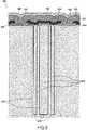
- FIG. 6is a cross section view 600 of an example distributed LC filter structure according to an embodiment.
- cross section view 600corresponds to a cross section of the LC filter structure illustrated in FIGs. 4 and 5 above along the line C-C' shown in FIG. 5 .
- first conductive layer 402, second conductive layer 406, and third conductive layer 408are disposed in a trench.
- First conductive layer 402 and second conductive layer 406are separated by the first insulator layer (not shown), and second conductive layer 406 and third conductive layer 408 are separated by the second insulator layer (not shown).
- Layer 604corresponds to the first insulation layer (first inter-metal dielectric) which is deposited above third conductive layer 408.
- Layer 604is deposited along the top surface of the substrate except for openings through which first, second, and third contact arrays CA1, CA2, and CA3 extend vertically to contact first conductive layer 402, second conductive layer 406, and third conductive layer 408, respectively.
- the pattern of layer 604is the complement of the aggregate pattern of contact arrays CA1, CA2, and CA3.
- two openings through layer 602 corresponding to second contact array CA2can be seen.
- First metal layer 502is disposed above layer 604 according to the pattern discussed above with respect to FIG. 5 .
- Layer 602corresponds to the second insulation layer (second inter-metal dielectric) which is deposited above first metal layer 502. As shown, layer 602 is deposited along the top surface of the substrate except for square openings corresponding to pattern 506 in FIG. 5 . This allows second metal layer 504 to contact second conductive layer 406.
- FIG. 7is a cross section view 700 of an example distributed LC filter structure according to an embodiment.
- cross sectionview 700corresponds to a cross section of the LC filter structure described with reference to FIGs. 4 and 5 above. For ease of presentation, trenches are not shown in cross section view 700.
- the distributed LC filter structureincludes a first conductive layer 702, a first insulator layer 704, a second conductive layer 706, a second insulator layer 708, a third conductive layer 710, a first insulation layer 712, a first metal layer 714, a second insulation layer 716, a second metal layer 718, a first contact array 724, a second contact array 720, and a third contact array 722.
- first conductive layer 702, second conductive layer 706, third conductive layer 710, first metal layer 714, second metal layer 718, first contact array 724, second contact array 720, and third contact array 722correspond respectively to first conductive layer 402, second conductive layer 406, third conductive layer 408, first metal layer 502, second metal layer 504, first contact array CA1, second contact array CA2, and third contact array CA3 described with reference to FIGs. 4 , 5 , and 6 above.
- first conductive layer 702is disposed on a top surface of a substrate (not shown).
- the substratehas a trench etched in its top surface and first conductive layer 702 is disposed into the trench.
- First insulator layer 704is disposed on top of first conductive layer 702, and second conductive layer 706 is disposed on top of first insulator layer 704.
- first insulator layer 704 and second conductive layer 706form a first insulator-metal structure of the distributed LC filter structure.
- the first insulator-metal structureis disposed in the trench etched into the substrate.
- Second insulator layer 708is disposed on top of second conductive layer 706, and third conductive layer 710 is disposed on top of second insulator layer 708.
- second insulator layer 708 and third conductive layer 710form a second insulator-metal structure of the distributed LC filter structure.
- the second insulator-metal structureis also disposed in the trench etched into the substrate.
- First insulation layer 712is deposited along the top surface of the substrate above third conductive layer 710, and first metal layer 714 is deposited on top of the first insulation layer 712.
- First contact array 724is formed to connect first metal layer 714 to first conductive layer 702
- third contact array 722is formed to connect first metal layer 714 to third conductive layer 710.
- Second insulation layer 716is deposited on top of the first metal layer 714, and second metal layer 718 is deposited on top of the second insulation layer 716.
- Second contact array 720is formed to connect second metal layer 718 to second conductive layer 706.
- second metal layer 718provides an inductance of the distributed LC filter structure.
- first conductive layer 702, second conductive layer 706, and third conductive layer 710provide first, second, and third electrodes, respectively, which form a first capacitive cell of the distributed LC filter.
- the first capacitive cellincludes a first capacitance formed by the first and second electrodes and a second capacitance formed by the second and third electrodes. Because the first and third electrodes are both connected to first metal layer 714, the first capacitance and the second capacitance are in parallel.
- the first, second, and third electrodesform a second capacitive cell (not shown) of the distributed LC filter, in parallel with the first capacitive cell.
- the second capacitance cellwould be located to the left or the right of the shown first capacitance cell.
- FIG. 9is a cross section view 900 of a non-uniformly distributed LC filter structure according to an embodiment. As shown in FIG. 9 , the capacitive cells are provided in a portion 902 and discontinued in a portion 904 of the structure. As such, in portion 904, only an inductance is formed. The resulting structure is therefore an LC+L structure.
- the distributed LC filter structurecan be designed to include an L+LC, an LC+L, or an L+LC+L filter structure.
- first metal layer 714is connected to a ground terminal via a ground path 728 and second metal layer 718 is connected to an input signal via a signal path 726.
- signal connectionsare designed so as to increase the mutual inductance between the ground path 728 and the signal path 726.
- signal connectionsare designed so as to reduce the mutual inductance between the ground path 802 and the signal path 726.
- a ground plane layer(not shown) is disposed above signal path 726 (i.e., above second metal layer 718). As such, the electromagnetic field is confined and interference with other components is reduced.
- EMIElectromagnetic Interference
- At least one of the first contact array 724, second contact array 720, and third contact array 722is configured such that a parasitic inductance of at least one of the first and second capacitive cells is coupled in series with the inductance provided by the second metal layer 718.
- at least one of the first contact array 724, second contact array 720, and third contact array 722may be configured such that a parasitic capacitance of second metal layer 718 is coupled in parallel with the first and second capacitive cells.
- the distributed LC filter structuremay be tuned to obtain a filter with an equivalent frequency response as a lumped LC filter. Additionally, the distributed capacitive design combined with a creative routing technique between capacitive cells permits a very flexible tuning of the filter envelope. The filter rejection may be increased while maintaining high efficiency and improving output ripples.
- the distributed LC structurehas been described for signal filtering use primarily.
- the structureis not limited to filtering applications and can be used in a variety of other applications as would be understood by a person of skill in the art.
- the structuremay be used to provide distributed capacitive decoupling along an interconnection line, a transmission line having strong capacitive coupling to ground, a low-pass single pole filter, or a low-pass cell in a higher pole order filter.
Landscapes
- Physics & Mathematics (AREA)
- Engineering & Computer Science (AREA)
- Power Engineering (AREA)
- Electromagnetism (AREA)
- Condensed Matter Physics & Semiconductors (AREA)
- General Physics & Mathematics (AREA)
- Computer Hardware Design (AREA)
- Microelectronics & Electronic Packaging (AREA)
- Semiconductor Integrated Circuits (AREA)
- Filters And Equalizers (AREA)
- Coils Or Transformers For Communication (AREA)
Description
- The present invention relates to integrated filter structures including inductance and capacitance components.
- Internet of Things (IoT) applications using communicating devices that are increasingly small, smart, and autonomous have been emerging recently. These applications are expected to drive innovation in the field of electronic integration for the next decade. Specifically, with key features of IoT devices being cost, size, and efficiency, the provision of highly efficient, highly integrated power supply circuitry is a main focus of research in IoT applications.
- In the general area of power supply, linear regulators have been replaced for many years now by switched inductive DC-DC buck converters operating at increasingly high frequencies.
FIG. 1 is a circuit diagram that illustrates anexample output stage 100 of a buck DC-DC converter. As shown inFIG. 1 ,output stage 100 includes aseries inductor 102, ashunt capacitor 104, and aload 106.Inductor 102 is coupled between an input terminal and an output terminal ofoutput stage 100. Typically,inductor 102 is associated with aparasitic resistance 110.Capacitor 104 is coupled in parallel toload 106, between the output terminal and a ground terminal. Typically,capacitor 104 is associated with aparasitic resistance 112 and aparasitic inductance 114. - In one filtering application, a square
wave input signal 108 is provided at the input terminal, for example by a switch.Input signal 108 is integrated byinductor 102 to produce a triangular wave signal.Capacitor 104 filters the triangular wave signal to generate a low-swing sinusoidal output signal acrossload 106. - Attempts atSiliconInPackage integration of buck converters have been limited. On one hand, this is because, conventionally,
inductor 102 andcapacitor 104 are made of discrete devices that cannot be easily integrated in package and/or above silicon for technological (e.g., thickness discrepancies, thermal expansion differences, etc.) and reliability reasons. Furthermore, with poor ESL (Equivalent Series Inductance) performance, integration with discrete passive components is limited in switching frequency to prevent unacceptable efficiency loss. However, as operating frequencies continue to increase, allowing for increasingly smaller passive values, interest in buck converter integration has been renewed. - Some efforts have focused on reducing inductor size and enhancing inductor leakage performance. Other efforts have been directed at reducing ESR (Equivalent Series Resistance) and ESL for capacitive components. Document
US 2017/104057 A1 describes a capacitor 3D-cell formed on a silicon substrate designed for producing low equivalent serial resistance and high capacitor surface-density. DocumentVOIRON FREDERIC ET AL: "Silicon high-density capacitors for power decoupling applications",2015 IEEE INTERNATIONAL WORKSHOP ON INTEGRATED POWER PACKAGING (IWIPP), IEEE, 3 May 2015 (2015-05-03), pages 48-51, XP032792512. describes a silicon-integrated capacitor enhanced for high temperature linearity and reliability and optimized for RL parasitic. For example,FIG. 2 is a cross-section view of a DC-DC converter 200 based on a Passive Integrated Common Substrate (PICS®) core distributed LC filter. As shown inFIG. 2 ,converter 200 includes adistributed capacitor structure 206 embedded in asilicon interposer 202. Distributedcapacitor structure 206 is designed to have reduced parasitics (i.e., low ESR and ESL). Adiscrete inductor 208 is stacked on top ofdistributed capacitor structure 206 to form a lumped LC filter. A Power Management Integrated Circuit (PMIC) 204 is flip-chip bonded ontosilicon interposer 202 such that the lumped LC filter is located closely underPMIC 204, reducing stray capacitance and allowing an ultra-low converter profile. Using such a design, a high efficiency converter operating at frequencies up to 100MHz can be achieved. - However, thus far, prior approaches have tended to optimize the inductor and the capacitor separately, leading to inefficient, heterogeneous integration of components manufactured in different process technologies, especially for low power converters. In addition, in PICS® designs such as shown in
FIG. 2 , efforts have focused on minimizing or cancelling the inductance resulting fromdistributed capacitor structure 206, treating it as a parasitic. - The present invention has been made in the light of the above problems.
- In one aspect, certain embodiments of the present invention enable a distributed LC filter structure providing simultaneously a distributed inductance and a distributed capacitance in the same structure. Accordingly, discrete passive elements are eliminated and high, homogenous integration is achieved. In certain embodiments according to another aspect of the invention, rather than treating the inductance resulting from the distributed capacitance as a parasitic (and attempting to reduce it), these embodiments tailor the interconnections between the distributed inductance and capacitance to leverage this parasitic inductance to increase the overall inductance of the distributed LC filter structure. Similarly, the interconnections between the distributed inductance and capacitance are tailored to leverage the parasitic capacitance resulting from the distributed inductance to add up with the distributed capacitance augmenting the overall capacitance of the structure.
- The present invention provides a distributed LC filter structure according to the present claims.
- In an embodiment, the distributed LC filter structure is used in a DC-DC converter such as a buck converter.
- Other features, elements, characteristics, and advantages of the present invention will become more apparent from the following detailed description of embodiments with reference to the attached drawings.
- The accompanying drawings illustrate certain embodiments of the present invention and, together with the description, serve to inform a person skilled in the art regarding how to put the invention into effect.
FIG. 1 is a circuit diagram that illustrates an example output stage of a buck DC-DC converter.FIG. 2 is a cross-section view of an example DC-DC converter based on a PICS® core lumped LC filter.FIG. 3 is a circuit diagram that illustrates an example distributed LC filter structure according to an embodiment.FIG. 4 is a top view of a first pattern layout of an example distributed LC filter structure according to an embodiment.FIG. 5 is a top view of a second pattern layout of an example distributed LC filter structure according to an embodiment.FIG. 6 is a cross section view of an example distributed LC filter structure according to an embodiment.FIG. 7 is a cross section view of an example distributed LC filter structure according to an embodiment.FIG. 8 is a cross section view of an example distributed LC filter structure according to an embodiment.FIG. 9 is a cross section view of an example distributed LC filter structure according to an embodiment.FIGs. 10A-G are top views illustrating a series of pattern layouts that may be used to form a distributed LC filter structure according to an embodiment.- The present disclosure will be described with reference to the accompanying drawings. Generally, the drawing in which an element first appears is typically indicated by the leftmost digit(s) in the corresponding reference number.
- Embodiments of the present invention overcome the deficiencies of prior solutions. In one aspect, the embodiments enable a distributed LC filter structure providing simultaneously a distributed inductance and a distributed capacitance in the same structure. Accordingly, discrete passive elements are eliminated and high, homogenous integration is achieved. In another aspect, rather than treating the inductance resulting from the distributed capacitance as a parasitic (and attempting to reduce it), embodiments tailor the interconnections between the distributed inductance and capacitance to leverage this parasitic inductance to increase the overall inductance of the distributed LC filter structure. Similarly, the interconnections between the distributed inductance and capacitance are tailored to leverage the parasitic capacitance resulting from the distributed inductance to add up with the distributed capacitance augmenting the overall capacitance of the structure.
FIG. 3 is a circuit diagram that illustrates an example distributedLC filter structure 300 according to an embodiment. DistributedLC filter structure 300 may be used as a low-pass filter, for example. In an embodiment, distributedLC filter structure 300 may be used as an output filtering stage of a DC-DC buck converter. In another embodiment, distributedLC filter structure 300 is coupled to a Power Management Integrated Circuit (PMIC) flip-chip bonded onto a substrate.- As shown in
FIG. 3 , exampleLC filter structure 300 includes a distributedinductor 302 and distributedcapacitor 304. Distributedinductor 302 includes a plurality of series inductive components 302-1, ..., 302-n. Each inductive component 302-1, ..., 302-n may have an associated parasitic resistance 306-1, ..., 306-n. Distributedcapacitor 304 includes a plurality of parallel capacitive components 304-1, ..., 304-n. Each capacitive component 304-1, ..., 304-n may have an associated parasitic resistance 308-1, ..., 308-n. Accordingly, distributedLC filter structure 300 is based on serializing the filter inductor in the horizontal path and parallelizing the shunt capacitor in the vertical path. - The plurality of inductive components 302-1, ..., 302-n may each further include a respective parasitic capacitance, and the plurality of capacitive components 304-1, ..., 304-n may each further include a respective parasitic inductance. In an embodiment (not shown in
FIG. 3 ), interconnections between distributedinductor 302 and distributedcapacitor 304 are made such that, in addition to enabling the circuit shown inFIG. 3 , they allow the parasitic capacitances of the plurality of inductive components 302-1, ..., 302-n to be coupled in parallel with the plurality of capacitive components 304-1, ..., 304-n. Additionally or alternatively, in another embodiment, the interconnections between distributedinductor 302 and distributedcapacitor 304 are made such that the parasitic inductances of the plurality of capacitive components 304-1, ..., 304-n are coupled in series with the plurality of inductive components 302-1, ..., 302-n. Accordingly, rather than attempting to reduce the parasitic inductance of the shunt capacitor and/or the parasitic capacitance of the filter inductor, the parasitics are leveraged to increase the filter inductance and/or the shunt capacitance of the LC filter. Performance of the resulting LC filter is thereby improved. FIGs. 4 and5 , further described below, illustrate pattern layouts of an example distributed LC filter structure according to an embodiment. The distributed LC filter structure illustrated inFIGs. 4 and5 may be an embodiment of distributedLC filter structure 300.FIG. 4 is a top view of afirst pattern layout 400 of the example distributed LC filter structure.First pattern layout 400 shows the layouts of atrench pattern 404, a firstconductive layer 402, a secondconductive layer 406, and a thirdconductive layer 408 of the LC filter structure. In an embodiment, firstconductive layer 402, secondconductive layer 406, and thirdconductive layer 408 provide first, second, and third electrodes that form at least one capacitive cell of the LC filter structure. For the purpose of presentation, intervening layers, such as isolation layers between the different conductive layers, are omitted.- In an embodiment,
trench pattern 404 is formed by etching a top surface of a substrate. Firstconductive layer 402 is then disposed over the top surface of the substrate and into the trenches formed bytrench pattern 404. A pattern layout resulting from firstconductive layer 402 andtrench pattern 404 is illustrated inFIG. 10A .Trench pattern 404 allows to extend, vertically into the substrate, the surfaces of the capacitors formed by the LC filter structure. As such, the capacitance of the resulting LC filter structure is increased. In another embodiment, however, the LC filter structure can be formed without etchingtrench pattern 404 into the substrate. - Returning to
FIG. 4 , after a first insulator layer (not shown) is disposed on top of firstconductive layer 404, secondconductive layer 406 is disposed on top of the first insulator layer, and into the trenches formed bytrench pattern 404, according to the shown pattern. In an embodiment, the first insulator layer and secondconductive layer 406 form a first insulator-metal structure of the LC filter structure. As shown inFIG. 4 , secondconductive layer 406 is disposed along the entire top surface of the substrate, save for first hexagonal areas that surround a first contact array CA1, disposed to connect firstconductive layer 402 to a first metal layer (not shown, discussed further below) of the structure.FIG. 10B illustrates a pattern layout resulting from firstconductive layer 402,trench pattern 404, and secondconductive layer 406. The first hexagonal areas that surround first contact area CA1 (not shown inFIG. 10B ) are denoted by thenumeral 1002. As would be understood by a person skilled in the art,areas 1002 may have other than a hexagonal shape, such as a square, rectangular, or circular shape for example. - Returning to
FIG. 4 , a second insulator layer (not shown) is then disposed on top of secondconductive layer 406, and thirdconductive layer 408 is disposed on top of the second insulator layer. Thirdconductive layer 408 is disposed into the trenches formed bytrench pattern 404. In an embodiment, the second insulator layer and thirdconductive layer 408 form a second insulator-metal structure of the LC filter structure. As shown inFIG. 4 , thirdconductive layer 408 is disposed along the entire top surface of the substrate, save for second hexagonal areas that surround the first contact array CA1 (the second hexagonal areas encompass the first hexagonal areas formed by the absence of second conductive layer 406) and third hexagonal areas that surround a second contact array CA2 disposed to connect secondconductive layer 406 to a second metal layer (discussed further below) of the structure. FIG. 10C illustrates a pattern layout resulting from firstconductive layer 402,trench pattern 404, secondconductive layer 406, and thirdconductive layer 408. The second hexagonal areas are denoted by the numeral 1006 and the third hexagonal areas are denoted by thenumeral 1004. As would be understood by a person skilled in the art,areas 1004 and/or 1006 may have other than a hexagonal shape, such as a square, rectangular, or circular shape for example.- Returning to
FIG. 4 , a third contact array CA3 is then disposed to connect thirdconductive layer 408 to the first metal of the structure as shown by the pattern CA3.FIG. 10D illustrates a pattern layout resulting from firstconductive layer 402,trench pattern 404, secondconductive layer 406, thirdconductive layer 408, first contact array CA1, second contact array CA2, and third contact array CA3. In an embodiment, first contact array CA1, second contact array CA2, and third contact array CA3 have equal contact density (defined as the number of contacts per surface unit). In another embodiment, first contact array CA1, second contact array CA2, and third contact array CA3 have equal contact surface (defined as the cumulative surface of contacts per surface unit). In a further embodiment, first contact array CA1, second contact array CA2, and third contact array CA3 have equal contact pitch (defined as the distance in between the contacts). In an embodiment, as shown inFIG. 10D , first contact array CA1 is staggered relative to second contact array CA2 and aligned horizontally with third contact array CA3, which is aligned vertically with second contact array CA2. FIG. 5 is a top view of asecond pattern layout 500 of an example distributed LC filter structure according to an embodiment.Second pattern layout 400 shows the layouts of afirst metal layer 502, asecond metal layer 504, and an inter-metal insulation layer of the LC filter structure.Second pattern layout 500 is a complementary layout tofirst pattern layout 400 shown inFIG. 4 , withsecond pattern layout 500 formed abovefirst pattern layout 400 in the distributed LC filter structure.- For ease of presentation, first
conductive layer 402 is shown inFIG. 5 as it defines the bottom most layer of the structure. - In an embodiment,
first metal layer 502 is deposited on top of a first insulation layer (not shown), which is deposited along the top surface of the substrate. In an embodiment, the first insulation layer is deposited along the entire top surface of the substrate, except in areas corresponding to the aggregate pattern formed by first contact array CA1, second contact array CA2, and third contact array CA3. - As shown in
FIG. 5 ,first metal layer 502 has a pattern that corresponds to the top surface of the substrate, save for areas in which the pattern is interrupted to form hexagonal shaped islands. FIG. 10E illustrates a pattern layout resulting from firstconductive layer 402,trench pattern 404,first metal layer 502, first contact array CA1, second contact array CA2, and third contact array CA3. In this pattern layout,first metal layer 502 includes islands that are rectangular shaped, instead of hexagonal shaped as inFIG. 5 .- Returning to
FIG. 5 , a second insulation layer (inter-metal dielectric) is then formed on top offirst metal layer 502. InFIG. 5 , the second insulation layer is formed along the entire surface of the substrate except for square openings defined bypattern 506. In an embodiment,pattern 506 corresponds to the location of second contact array CA2, which as mentioned above, connects secondconductive layer 506 tosecond metal layer 504. - A pattern layout resulting from first
conductive layer 402,trench pattern 404,first metal layer 502, and the second insulation layer is shown inFIG. 10F according to an embodiment. As shown inFIG. 10F , in this embodiment, thepattern 506 further includes bands in which the second insulation layer is also interrupted. - Returning to
FIG. 5 ,second metal layer 504 is then deposited on top of the second insulation layer. As shown inFIG. 5 ,second metal layer 504 has a linear shape with a length (I) and a width (W) with I being larger than W by a factor of at least 100. A pattern layout resulting fromtrench pattern 404,first metal layer 502,second metal layer 504, and the second insulation layer is shown inFIG. 10G . - In an embodiment,
second metal layer 504 serves to provide a distributed inductance of the distributed LC filter structure. The inductance value L is related to the length I and the width W by the equation L = f(I/W), where f represents the frequency. In other embodiment,second metal layer 504 can have different layouts, like a meander pattern, a planar loop, or a spiral. FIG. 6 is across section view 600 of an example distributed LC filter structure according to an embodiment. In an embodiment,cross section view 600 corresponds to a cross section of the LC filter structure illustrated inFIGs. 4 and5 above along the line C-C' shown inFIG. 5 .- As shown in
FIG. 6 , firstconductive layer 402, secondconductive layer 406, and thirdconductive layer 408 are disposed in a trench. Firstconductive layer 402 and secondconductive layer 406 are separated by the first insulator layer (not shown), and secondconductive layer 406 and thirdconductive layer 408 are separated by the second insulator layer (not shown). Layer 604 corresponds to the first insulation layer (first inter-metal dielectric) which is deposited above thirdconductive layer 408.Layer 604 is deposited along the top surface of the substrate except for openings through which first, second, and third contact arrays CA1, CA2, and CA3 extend vertically to contact firstconductive layer 402, secondconductive layer 406, and thirdconductive layer 408, respectively. In other words, the pattern oflayer 604 is the complement of the aggregate pattern of contact arrays CA1, CA2, and CA3. InFIG. 6 , two openings throughlayer 602 corresponding to second contact array CA2 can be seen.First metal layer 502 is disposed abovelayer 604 according to the pattern discussed above with respect toFIG. 5 .Layer 602 corresponds to the second insulation layer (second inter-metal dielectric) which is deposited abovefirst metal layer 502. As shown,layer 602 is deposited along the top surface of the substrate except for square openings corresponding topattern 506 inFIG. 5 . This allowssecond metal layer 504 to contact secondconductive layer 406.FIG. 7 is across section view 700 of an example distributed LC filter structure according to an embodiment. In an embodiment, crosssectionview 700 corresponds to a cross section of the LC filter structure described with reference toFIGs. 4 and5 above. For ease of presentation, trenches are not shown incross section view 700.- As shown in
FIG. 7 , the distributed LC filter structure includes a firstconductive layer 702, afirst insulator layer 704, a secondconductive layer 706, asecond insulator layer 708, a thirdconductive layer 710, afirst insulation layer 712, afirst metal layer 714, asecond insulation layer 716, asecond metal layer 718, afirst contact array 724, asecond contact array 720, and athird contact array 722. - In an embodiment, first
conductive layer 702, secondconductive layer 706, thirdconductive layer 710,first metal layer 714,second metal layer 718,first contact array 724,second contact array 720, andthird contact array 722 correspond respectively to firstconductive layer 402, secondconductive layer 406, thirdconductive layer 408,first metal layer 502,second metal layer 504, first contact array CA1, second contact array CA2, and third contact array CA3 described with reference toFIGs. 4 ,5 , and6 above. - In an embodiment, first
conductive layer 702 is disposed on a top surface of a substrate (not shown). In another embodiment, the substrate has a trench etched in its top surface and firstconductive layer 702 is disposed into the trench. First insulator layer 704 is disposed on top of firstconductive layer 702, and secondconductive layer 706 is disposed on top offirst insulator layer 704. In an embodiment,first insulator layer 704 and secondconductive layer 706 form a first insulator-metal structure of the distributed LC filter structure. In an embodiment, the first insulator-metal structure is disposed in the trench etched into the substrate.Second insulator layer 708 is disposed on top of secondconductive layer 706, and thirdconductive layer 710 is disposed on top ofsecond insulator layer 708. In an embodiment,second insulator layer 708 and thirdconductive layer 710 form a second insulator-metal structure of the distributed LC filter structure. In an embodiment, the second insulator-metal structure is also disposed in the trench etched into the substrate.First insulation layer 712 is deposited along the top surface of the substrate above thirdconductive layer 710, andfirst metal layer 714 is deposited on top of thefirst insulation layer 712.First contact array 724 is formed to connectfirst metal layer 714 to firstconductive layer 702, andthird contact array 722 is formed to connectfirst metal layer 714 to thirdconductive layer 710.Second insulation layer 716 is deposited on top of thefirst metal layer 714, andsecond metal layer 718 is deposited on top of thesecond insulation layer 716.Second contact array 720 is formed to connectsecond metal layer 718 to secondconductive layer 706. In an embodiment,second metal layer 718 provides an inductance of the distributed LC filter structure.- In an embodiment, first
conductive layer 702, secondconductive layer 706, and thirdconductive layer 710 provide first, second, and third electrodes, respectively, which form a first capacitive cell of the distributed LC filter. As shown inFIG. 7 , the first capacitive cell includes a first capacitance formed by the first and second electrodes and a second capacitance formed by the second and third electrodes. Because the first and third electrodes are both connected tofirst metal layer 714, the first capacitance and the second capacitance are in parallel. - In another embodiment, the first, second, and third electrodes form a second capacitive cell (not shown) of the distributed LC filter, in parallel with the first capacitive cell. In
cross section view 700 ofFIG. 7 , the second capacitance cell would be located to the left or the right of the shown first capacitance cell. - In a further embodiment, parallel capacitive cells underlie the entire length of
second metal layer 718 to create a uniformly distributed structure. In another embodiment, the capacitive cells underlie only a portion ofsecond metal layer 718 to create a non-uniformly distributed structure. For example,FIG. 9 is across section view 900 of a non-uniformly distributed LC filter structure according to an embodiment. As shown inFIG. 9 , the capacitive cells are provided in aportion 902 and discontinued in aportion 904 of the structure. As such, inportion 904, only an inductance is formed. The resulting structure is therefore an LC+L structure. As would be understood by a person of skill in the art based on the teachings herein, other structures can be formed by forming/interrupting the formation of capacitive cells in one or more portions of the structure. For example, the distributed LC filter structure can be designed to include an L+LC, an LC+L, or an L+LC+L filter structure. - In an embodiment, as shown in
FIG. 7 for example,first metal layer 714 is connected to a ground terminal via aground path 728 andsecond metal layer 718 is connected to an input signal via asignal path 726. In one implementation, as inFIG. 7 , signal connections are designed so as to increase the mutual inductance between theground path 728 and thesignal path 726. In another implementation, shown inFIG. 8 , signal connections are designed so as to reduce the mutual inductance between theground path 802 and thesignal path 726. - In another embodiment, in order to enhance the LC distributed filter structure from an Electromagnetic Interference (EMI) emission point of view, especially at high frequency, a ground plane layer (not shown) is disposed above signal path 726 (i.e., above second metal layer 718). As such, the electromagnetic field is confined and interference with other components is reduced.
- In an embodiment, at least one of the
first contact array 724,second contact array 720, andthird contact array 722 is configured such that a parasitic inductance of at least one of the first and second capacitive cells is coupled in series with the inductance provided by thesecond metal layer 718. Alternatively or additionally, at least one of thefirst contact array 724,second contact array 720, andthird contact array 722 may be configured such that a parasitic capacitance ofsecond metal layer 718 is coupled in parallel with the first and second capacitive cells. - In embodiments, the distributed LC filter structure may be tuned to obtain a filter with an equivalent frequency response as a lumped LC filter. Additionally, the distributed capacitive design combined with a creative routing technique between capacitive cells permits a very flexible tuning of the filter envelope. The filter rejection may be increased while maintaining high efficiency and improving output ripples.
- In the embodiments above, the distributed LC structure has been described for signal filtering use primarily. However, the structure is not limited to filtering applications and can be used in a variety of other applications as would be understood by a person of skill in the art. For example, the structure may be used to provide distributed capacitive decoupling along an interconnection line, a transmission line having strong capacitive coupling to ground, a low-pass single pole filter, or a low-pass cell in a higher pole order filter.
Claims (12)
- A distributed LC filter structure, comprising:a substrate having a trench etched in a top surface thereof;a first conductive layer (702) disposed in the trench;a first insulator-metal structure disposed in the trench on top of the first conductive layer (702), the first insulator-metal structure comprising a first insulator layer (704) disposed on top of the first conductive layer (702) and a second conductive layer (706) disposed on top of the first insulator layer (704);a second insulator-metal structure disposed in the trench on top of the first insulator-metal structure, the second insulator-metal structure comprising a second insulator layer (708) disposed on top of the second conductive layer (706) and a third conductive layer (710) disposed on top of the second insulator layer (706);a first insulation layer (712) deposited along the top surface of the substrate above the third conductive layer (710);a first metal layer (714) deposited on top of the first insulation layer (712);a second insulation layer (716) deposited on top of the first metal layer (714);a second metal layer (718) deposited on top of the second insulation layer (716);a first contact array (724) connecting the first conductive layer (702) to the first metal layer (714);a second contact array (720) connecting the second conductive layer (706) to the second metal layer (718); anda third contact array (722) connecting the third conductive layer (710) to the first metal layer (714),wherein the first conductive layer (702), the second conductive layer (706), and the third conductive layer (710) provide first, second, and third electrodes, respectively, the first, second, and third electrodes forming a first capacitive cell of the distributed LC filter; the second metal layer (718) has a length and a width, the length being larger than the width by a factor of at least 100 and that the second metal layer (718) provides an inductance of the distributed LC filter structure.
- The distributed LC filter structure of claim 1, wherein the first, second, and third electrodes form a second capacitive cell of the distributed LC filter, the second capacitive cell being in parallel with the first capacitive cell.
- The distributed LC filter structure of claim 2, wherein in at least one of the first and second capacitive cells, the first and second electrodes form a first capacitance and the second and third electrodes form a second capacitance, the first capacitance being in parallel with the second capacitance.
- The distributed LC filter structure of claim 1, wherein at least one of the first contact array (724), the second contact array (720), and the third contact array (722) is configured such that a parasitic inductance of at least one of the first and second capacitive cells is coupled in series with the inductance provided by the second metal layer (718).
- The distributed LC filter structure of any of claims 1 and 4, wherein the first and second capacitive cells underlie the entire length of the second metal layer (718), thereby forming a uniformly distributed LC structure.
- The distributed LC filter structure of any of claims 1 and 4, wherein the first and second capacitive cells underlie only a portion of the entire length of the second metal layer (718).
- The distributed LC filter structure of claim 6, wherein the distributed LC filter structure includes one of a L+LC, a LC+L, or a L+LC+L filter.
- The distributed LC filter structure of any of claims 1-7, wherein the first metal layer (714) is connected to a ground terminal and the second metal layer (718) is connected to an input signal terminal.
- The distributed LC filter structure of any of claims 1-8, wherein the first contact array (724), the second contact array (720), and the third contact array (722) have equal contact density.
- The distributed LC filter structure of any of claims 1-9, wherein the first contact array (724), the second contact array (720), and the third contact array (722) have equal pitch.
- The distributed LC filter structure of any of claims 1-10, wherein the distributed LC filter structure is coupled to a Power Management Integrated Circuit (PMIC) flip-chip bonded onto the substrate.
- A DC-DC converter comprising a distributed LC filter structure according to any of claims 1-11.
Priority Applications (6)
| Application Number | Priority Date | Filing Date | Title |
|---|---|---|---|
| EP17305846.2AEP3422417B1 (en) | 2017-06-30 | 2017-06-30 | Distributed lc filter structure |
| TW107121726ATWI761540B (en) | 2017-06-30 | 2018-06-25 | Distributed lc filter structure |
| PCT/IB2018/000690WO2019002931A1 (en) | 2017-06-30 | 2018-06-29 | Distributed lc filter structure |
| CN201880049558.5ACN110959197B (en) | 2017-06-30 | 2018-06-29 | Distributed LC filter structure |
| US16/728,403US10903538B2 (en) | 2017-06-30 | 2019-12-27 | Distributed LC filter structure |
| US17/130,715US11862834B2 (en) | 2017-06-30 | 2020-12-22 | Distributed LC filter structure |
Applications Claiming Priority (1)
| Application Number | Priority Date | Filing Date | Title |
|---|---|---|---|
| EP17305846.2AEP3422417B1 (en) | 2017-06-30 | 2017-06-30 | Distributed lc filter structure |
Publications (2)
| Publication Number | Publication Date |
|---|---|
| EP3422417A1 EP3422417A1 (en) | 2019-01-02 |
| EP3422417B1true EP3422417B1 (en) | 2021-08-04 |
Family
ID=59772543
Family Applications (1)
| Application Number | Title | Priority Date | Filing Date |
|---|---|---|---|
| EP17305846.2AActiveEP3422417B1 (en) | 2017-06-30 | 2017-06-30 | Distributed lc filter structure |
Country Status (5)
| Country | Link |
|---|---|
| US (2) | US10903538B2 (en) |
| EP (1) | EP3422417B1 (en) |
| CN (1) | CN110959197B (en) |
| TW (1) | TWI761540B (en) |
| WO (1) | WO2019002931A1 (en) |
Families Citing this family (6)
| Publication number | Priority date | Publication date | Assignee | Title |
|---|---|---|---|---|
| EP3422417B1 (en)* | 2017-06-30 | 2021-08-04 | Murata Manufacturing Co., Ltd. | Distributed lc filter structure |
| WO2020217850A1 (en)* | 2019-04-24 | 2020-10-29 | 株式会社村田製作所 | Capacitor |
| CN111478575B (en)* | 2020-04-30 | 2021-05-25 | 北京理工大学 | A Design Method of High Voltage Power Supply Electromagnetic Interference Filter |
| CN111478576B (en)* | 2020-04-30 | 2021-05-25 | 北京理工大学 | Filter design method |
| JP2023049959A (en)* | 2021-09-29 | 2023-04-10 | ローム株式会社 | chip parts |
| CN115579348A (en)* | 2022-10-26 | 2023-01-06 | 华进半导体封装先导技术研发中心有限公司 | Adapter plate structure and preparation method thereof |
Family Cites Families (24)
| Publication number | Priority date | Publication date | Assignee | Title |
|---|---|---|---|---|
| US6731184B1 (en)* | 1999-07-29 | 2004-05-04 | Murata Manufacturing Co., Ltd. | High frequency switching component |
| US6552696B1 (en)* | 2000-03-29 | 2003-04-22 | Hrl Laboratories, Llc | Electronically tunable reflector |
| US6624500B2 (en)* | 2000-11-30 | 2003-09-23 | Kyocera Corporation | Thin-film electronic component and motherboard |
| US6864669B1 (en)* | 2002-05-02 | 2005-03-08 | O2Micro International Limited | Power supply block with simplified switch configuration |
| JP4843930B2 (en)* | 2004-10-27 | 2011-12-21 | 富士電機株式会社 | Semiconductor device and manufacturing method thereof |
| WO2007000697A2 (en)* | 2005-06-29 | 2007-01-04 | Koninklijke Philips Electronics N.V. | Method of manufacturing an assembly and assembly |
| WO2007054858A2 (en)* | 2005-11-08 | 2007-05-18 | Nxp B.V. | Integrated capacitor arrangement for ultrahigh capacitance values |
| US20070218699A1 (en)* | 2006-03-16 | 2007-09-20 | Tokyo Electron Limited | Plasma etching method and computer-readable storage medium |
| WO2007115255A2 (en)* | 2006-03-31 | 2007-10-11 | University Of Florida Research Foundation, Inc. | Integrated power passives |
| US20070246805A1 (en)* | 2006-04-25 | 2007-10-25 | Ligang Zhang | Multi-die inductor |
| JP5612268B2 (en)* | 2008-03-28 | 2014-10-22 | 株式会社東芝 | Semiconductor device and DC-DC converter |
| US8120142B2 (en)* | 2008-04-18 | 2012-02-21 | Alpha & Omega Semiconductor, Ltd. | Applying trenched transient voltage suppressor (TVS) technology for distributed low pass filters |
| JP5127060B2 (en)* | 2008-12-08 | 2013-01-23 | スミダコーポレーション株式会社 | Variable inductor |
| JP5540912B2 (en)* | 2009-08-12 | 2014-07-02 | 株式会社村田製作所 | Multilayer filter |
| US8502340B2 (en)* | 2010-12-09 | 2013-08-06 | Tessera, Inc. | High density three-dimensional integrated capacitors |
| US20130146345A1 (en)* | 2011-12-12 | 2013-06-13 | Kazuki KAJIHARA | Printed wiring board and method for manufacturing the same |
| US9048809B2 (en)* | 2012-01-03 | 2015-06-02 | International Business Machines Corporation | Method of manufacturing switchable filters |
| RU2708638C2 (en)* | 2015-07-09 | 2019-12-10 | Констрюксьон Электроник Плюс Телекоммюникасьон | Inverter with high specific power |
| US9647057B2 (en)* | 2015-10-08 | 2017-05-09 | Ipdia | Capacitor 3D-cell and 3D-capacitor structure |
| US10420171B2 (en)* | 2016-08-26 | 2019-09-17 | Qualcomm Incorporated | Semiconductor devices on two sides of an isolation layer |
| US9917062B1 (en)* | 2016-09-15 | 2018-03-13 | Qualcomm Incorporated | Self-aligned transistors for dual-side processing |
| EP3422417B1 (en)* | 2017-06-30 | 2021-08-04 | Murata Manufacturing Co., Ltd. | Distributed lc filter structure |
| WO2019065419A1 (en)* | 2017-09-29 | 2019-04-04 | 株式会社村田製作所 | High frequency module and communication device |
| EP3799084B1 (en)* | 2019-09-30 | 2023-05-03 | Murata Manufacturing Co., Ltd. | Nanomagnetic inductor cores, inductors and devices incorporating such cores, and associated manufacturing methods |
- 2017
- 2017-06-30EPEP17305846.2Apatent/EP3422417B1/enactiveActive
- 2018
- 2018-06-25TWTW107121726Apatent/TWI761540B/enactive
- 2018-06-29CNCN201880049558.5Apatent/CN110959197B/enactiveActive
- 2018-06-29WOPCT/IB2018/000690patent/WO2019002931A1/ennot_activeCeased
- 2019
- 2019-12-27USUS16/728,403patent/US10903538B2/enactiveActive
- 2020
- 2020-12-22USUS17/130,715patent/US11862834B2/enactiveActive
Non-Patent Citations (1)
| Title |
|---|
| None* |
Also Published As
| Publication number | Publication date |
|---|---|
| TWI761540B (en) | 2022-04-21 |
| US20200136221A1 (en) | 2020-04-30 |
| CN110959197B (en) | 2023-08-08 |
| US11862834B2 (en) | 2024-01-02 |
| EP3422417A1 (en) | 2019-01-02 |
| TW201906167A (en) | 2019-02-01 |
| US20210111468A1 (en) | 2021-04-15 |
| US10903538B2 (en) | 2021-01-26 |
| CN110959197A (en) | 2020-04-03 |
| WO2019002931A1 (en) | 2019-01-03 |
Similar Documents
| Publication | Publication Date | Title |
|---|---|---|
| EP3422417B1 (en) | Distributed lc filter structure | |
| US6075427A (en) | MCM with high Q overlapping resonator | |
| CN101461060B (en) | Improved Interdigitated Metal-Insulator-Metal Capacitor and Its Capacitor Array | |
| US20070217122A1 (en) | Capacitor | |
| US9159718B2 (en) | Switched capacitor structure | |
| CN202905470U (en) | Multilayer silicon-based capacitor electrode connection structure | |
| JP5637150B2 (en) | Multilayer bandpass filter | |
| TW201541598A (en) | Semiconductor device with inductor-capacitor resonant circuit | |
| CN117155338A (en) | Hybrid filter | |
| US8373252B1 (en) | Integrated circuit having capacitor on back surface | |
| US8405453B2 (en) | Millimeter-wave on-chip switch employing frequency-dependent inductance for cancellation of off-state capacitance | |
| US7893795B2 (en) | Circuit device having inductor and capacitor in parallel connection | |
| CN101847627A (en) | Semiconductor chip of integrated passive device and power amplifier device | |
| US9660019B2 (en) | Concentric capacitor structure | |
| CN212113714U (en) | Radio frequency front-end module, radio frequency communication device and electronic equipment | |
| US8107215B2 (en) | Capacitor | |
| CN114582860B (en) | A multi-capacitance matching MOM capacitor | |
| JP2010135453A (en) | Semiconductor device, and method of manufacturing the same | |
| JP6103252B2 (en) | Dielectric resonator and electronic component | |
| JP2005527165A (en) | Decoupling module for disconnecting high-frequency signals from power lines | |
| KR101102306B1 (en) | Internal Matching Structure of BANN Amplifier Using LTC | |
| CN101471468B (en) | planar inductively coupled structure | |
| KR20090053584A (en) | Multilayer Printed Circuit Board with Passive Device and Manufacturing Method | |
| CN115084375A (en) | A design method for ultra-thin 3D inductive passive devices |
Legal Events
| Date | Code | Title | Description |
|---|---|---|---|
| PUAI | Public reference made under article 153(3) epc to a published international application that has entered the european phase | Free format text:ORIGINAL CODE: 0009012 | |
| STAA | Information on the status of an ep patent application or granted ep patent | Free format text:STATUS: THE APPLICATION HAS BEEN PUBLISHED | |
| AK | Designated contracting states | Kind code of ref document:A1 Designated state(s):AL AT BE BG CH CY CZ DE DK EE ES FI FR GB GR HR HU IE IS IT LI LT LU LV MC MK MT NL NO PL PT RO RS SE SI SK SM TR | |
| AX | Request for extension of the european patent | Extension state:BA ME | |
| STAA | Information on the status of an ep patent application or granted ep patent | Free format text:STATUS: REQUEST FOR EXAMINATION WAS MADE | |
| 17P | Request for examination filed | Effective date:20190628 | |
| RBV | Designated contracting states (corrected) | Designated state(s):AL AT BE BG CH CY CZ DE DK EE ES FI FR GB GR HR HU IE IS IT LI LT LU LV MC MK MT NL NO PL PT RO RS SE SI SK SM TR | |
| STAA | Information on the status of an ep patent application or granted ep patent | Free format text:STATUS: EXAMINATION IS IN PROGRESS | |
| 17Q | First examination report despatched | Effective date:20200325 | |
| RIC1 | Information provided on ipc code assigned before grant | Ipc:H03H 7/01 20060101ALI20210120BHEP Ipc:H02M 1/44 20070101ALI20210120BHEP Ipc:H01L 29/66 20060101AFI20210120BHEP Ipc:H01L 27/01 20060101ALI20210120BHEP Ipc:H01L 49/02 20060101ALI20210120BHEP | |
| GRAP | Despatch of communication of intention to grant a patent | Free format text:ORIGINAL CODE: EPIDOSNIGR1 | |
| STAA | Information on the status of an ep patent application or granted ep patent | Free format text:STATUS: GRANT OF PATENT IS INTENDED | |
| INTG | Intention to grant announced | Effective date:20210315 | |
| GRAS | Grant fee paid | Free format text:ORIGINAL CODE: EPIDOSNIGR3 | |
| GRAA | (expected) grant | Free format text:ORIGINAL CODE: 0009210 | |
| STAA | Information on the status of an ep patent application or granted ep patent | Free format text:STATUS: THE PATENT HAS BEEN GRANTED | |
| AK | Designated contracting states | Kind code of ref document:B1 Designated state(s):AL AT BE BG CH CY CZ DE DK EE ES FI FR GB GR HR HU IE IS IT LI LT LU LV MC MK MT NL NO PL PT RO RS SE SI SK SM TR | |
| REG | Reference to a national code | Ref country code:GB Ref legal event code:FG4D | |
| REG | Reference to a national code | Ref country code:AT Ref legal event code:REF Ref document number:1417882 Country of ref document:AT Kind code of ref document:T Effective date:20210815 | |
| REG | Reference to a national code | Ref country code:CH Ref legal event code:EP | |
| REG | Reference to a national code | Ref country code:DE Ref legal event code:R096 Ref document number:602017043280 Country of ref document:DE | |
| REG | Reference to a national code | Ref country code:IE Ref legal event code:FG4D | |
| REG | Reference to a national code | Ref country code:LT Ref legal event code:MG9D | |
| REG | Reference to a national code | Ref country code:NL Ref legal event code:MP Effective date:20210804 | |
| REG | Reference to a national code | Ref country code:AT Ref legal event code:MK05 Ref document number:1417882 Country of ref document:AT Kind code of ref document:T Effective date:20210804 | |
| PG25 | Lapsed in a contracting state [announced via postgrant information from national office to epo] | Ref country code:SE Free format text:LAPSE BECAUSE OF FAILURE TO SUBMIT A TRANSLATION OF THE DESCRIPTION OR TO PAY THE FEE WITHIN THE PRESCRIBED TIME-LIMIT Effective date:20210804 Ref country code:RS Free format text:LAPSE BECAUSE OF FAILURE TO SUBMIT A TRANSLATION OF THE DESCRIPTION OR TO PAY THE FEE WITHIN THE PRESCRIBED TIME-LIMIT Effective date:20210804 Ref country code:HR Free format text:LAPSE BECAUSE OF FAILURE TO SUBMIT A TRANSLATION OF THE DESCRIPTION OR TO PAY THE FEE WITHIN THE PRESCRIBED TIME-LIMIT Effective date:20210804 Ref country code:BG Free format text:LAPSE BECAUSE OF FAILURE TO SUBMIT A TRANSLATION OF THE DESCRIPTION OR TO PAY THE FEE WITHIN THE PRESCRIBED TIME-LIMIT Effective date:20211104 Ref country code:AT Free format text:LAPSE BECAUSE OF FAILURE TO SUBMIT A TRANSLATION OF THE DESCRIPTION OR TO PAY THE FEE WITHIN THE PRESCRIBED TIME-LIMIT Effective date:20210804 Ref country code:LT Free format text:LAPSE BECAUSE OF FAILURE TO SUBMIT A TRANSLATION OF THE DESCRIPTION OR TO PAY THE FEE WITHIN THE PRESCRIBED TIME-LIMIT Effective date:20210804 Ref country code:NO Free format text:LAPSE BECAUSE OF FAILURE TO SUBMIT A TRANSLATION OF THE DESCRIPTION OR TO PAY THE FEE WITHIN THE PRESCRIBED TIME-LIMIT Effective date:20211104 Ref country code:PT Free format text:LAPSE BECAUSE OF FAILURE TO SUBMIT A TRANSLATION OF THE DESCRIPTION OR TO PAY THE FEE WITHIN THE PRESCRIBED TIME-LIMIT Effective date:20211206 Ref country code:FI Free format text:LAPSE BECAUSE OF FAILURE TO SUBMIT A TRANSLATION OF THE DESCRIPTION OR TO PAY THE FEE WITHIN THE PRESCRIBED TIME-LIMIT Effective date:20210804 Ref country code:ES Free format text:LAPSE BECAUSE OF FAILURE TO SUBMIT A TRANSLATION OF THE DESCRIPTION OR TO PAY THE FEE WITHIN THE PRESCRIBED TIME-LIMIT Effective date:20210804 | |
| PG25 | Lapsed in a contracting state [announced via postgrant information from national office to epo] | Ref country code:PL Free format text:LAPSE BECAUSE OF FAILURE TO SUBMIT A TRANSLATION OF THE DESCRIPTION OR TO PAY THE FEE WITHIN THE PRESCRIBED TIME-LIMIT Effective date:20210804 Ref country code:LV Free format text:LAPSE BECAUSE OF FAILURE TO SUBMIT A TRANSLATION OF THE DESCRIPTION OR TO PAY THE FEE WITHIN THE PRESCRIBED TIME-LIMIT Effective date:20210804 Ref country code:GR Free format text:LAPSE BECAUSE OF FAILURE TO SUBMIT A TRANSLATION OF THE DESCRIPTION OR TO PAY THE FEE WITHIN THE PRESCRIBED TIME-LIMIT Effective date:20211105 | |
| PG25 | Lapsed in a contracting state [announced via postgrant information from national office to epo] | Ref country code:NL Free format text:LAPSE BECAUSE OF FAILURE TO SUBMIT A TRANSLATION OF THE DESCRIPTION OR TO PAY THE FEE WITHIN THE PRESCRIBED TIME-LIMIT Effective date:20210804 | |
| PG25 | Lapsed in a contracting state [announced via postgrant information from national office to epo] | Ref country code:DK Free format text:LAPSE BECAUSE OF FAILURE TO SUBMIT A TRANSLATION OF THE DESCRIPTION OR TO PAY THE FEE WITHIN THE PRESCRIBED TIME-LIMIT Effective date:20210804 | |
| REG | Reference to a national code | Ref country code:DE Ref legal event code:R097 Ref document number:602017043280 Country of ref document:DE | |
| PG25 | Lapsed in a contracting state [announced via postgrant information from national office to epo] | Ref country code:SM Free format text:LAPSE BECAUSE OF FAILURE TO SUBMIT A TRANSLATION OF THE DESCRIPTION OR TO PAY THE FEE WITHIN THE PRESCRIBED TIME-LIMIT Effective date:20210804 Ref country code:SK Free format text:LAPSE BECAUSE OF FAILURE TO SUBMIT A TRANSLATION OF THE DESCRIPTION OR TO PAY THE FEE WITHIN THE PRESCRIBED TIME-LIMIT Effective date:20210804 Ref country code:RO Free format text:LAPSE BECAUSE OF FAILURE TO SUBMIT A TRANSLATION OF THE DESCRIPTION OR TO PAY THE FEE WITHIN THE PRESCRIBED TIME-LIMIT Effective date:20210804 Ref country code:EE Free format text:LAPSE BECAUSE OF FAILURE TO SUBMIT A TRANSLATION OF THE DESCRIPTION OR TO PAY THE FEE WITHIN THE PRESCRIBED TIME-LIMIT Effective date:20210804 Ref country code:CZ Free format text:LAPSE BECAUSE OF FAILURE TO SUBMIT A TRANSLATION OF THE DESCRIPTION OR TO PAY THE FEE WITHIN THE PRESCRIBED TIME-LIMIT Effective date:20210804 Ref country code:AL Free format text:LAPSE BECAUSE OF FAILURE TO SUBMIT A TRANSLATION OF THE DESCRIPTION OR TO PAY THE FEE WITHIN THE PRESCRIBED TIME-LIMIT Effective date:20210804 | |
| PLBE | No opposition filed within time limit | Free format text:ORIGINAL CODE: 0009261 | |
| STAA | Information on the status of an ep patent application or granted ep patent | Free format text:STATUS: NO OPPOSITION FILED WITHIN TIME LIMIT | |
| 26N | No opposition filed | Effective date:20220506 | |
| PG25 | Lapsed in a contracting state [announced via postgrant information from national office to epo] | Ref country code:SI Free format text:LAPSE BECAUSE OF FAILURE TO SUBMIT A TRANSLATION OF THE DESCRIPTION OR TO PAY THE FEE WITHIN THE PRESCRIBED TIME-LIMIT Effective date:20210804 | |
| PG25 | Lapsed in a contracting state [announced via postgrant information from national office to epo] | Ref country code:MC Free format text:LAPSE BECAUSE OF FAILURE TO SUBMIT A TRANSLATION OF THE DESCRIPTION OR TO PAY THE FEE WITHIN THE PRESCRIBED TIME-LIMIT Effective date:20210804 | |
| REG | Reference to a national code | Ref country code:CH Ref legal event code:PL | |
| REG | Reference to a national code | Ref country code:BE Ref legal event code:MM Effective date:20220630 | |
| GBPC | Gb: european patent ceased through non-payment of renewal fee | Effective date:20220630 | |
| REG | Reference to a national code | Ref country code:DE Ref legal event code:R082 Ref document number:602017043280 Country of ref document:DE Representative=s name:CBDL PATENTANWAELTE GBR, DE Ref country code:DE Ref legal event code:R082 Ref document number:602017043280 Country of ref document:DE Representative=s name:CBDL PATENTANWAELTE EGBR, DE | |
| PG25 | Lapsed in a contracting state [announced via postgrant information from national office to epo] | Ref country code:LU Free format text:LAPSE BECAUSE OF NON-PAYMENT OF DUE FEES Effective date:20220630 Ref country code:LI Free format text:LAPSE BECAUSE OF NON-PAYMENT OF DUE FEES Effective date:20220630 Ref country code:IE Free format text:LAPSE BECAUSE OF NON-PAYMENT OF DUE FEES Effective date:20220630 Ref country code:CH Free format text:LAPSE BECAUSE OF NON-PAYMENT OF DUE FEES Effective date:20220630 | |
| PG25 | Lapsed in a contracting state [announced via postgrant information from national office to epo] | Ref country code:GB Free format text:LAPSE BECAUSE OF NON-PAYMENT OF DUE FEES Effective date:20220630 Ref country code:BE Free format text:LAPSE BECAUSE OF NON-PAYMENT OF DUE FEES Effective date:20220630 | |
| PG25 | Lapsed in a contracting state [announced via postgrant information from national office to epo] | Ref country code:HU Free format text:LAPSE BECAUSE OF FAILURE TO SUBMIT A TRANSLATION OF THE DESCRIPTION OR TO PAY THE FEE WITHIN THE PRESCRIBED TIME-LIMIT; INVALID AB INITIO Effective date:20170630 | |
| PG25 | Lapsed in a contracting state [announced via postgrant information from national office to epo] | Ref country code:MK Free format text:LAPSE BECAUSE OF FAILURE TO SUBMIT A TRANSLATION OF THE DESCRIPTION OR TO PAY THE FEE WITHIN THE PRESCRIBED TIME-LIMIT Effective date:20210804 Ref country code:CY Free format text:LAPSE BECAUSE OF FAILURE TO SUBMIT A TRANSLATION OF THE DESCRIPTION OR TO PAY THE FEE WITHIN THE PRESCRIBED TIME-LIMIT Effective date:20210804 | |
| PG25 | Lapsed in a contracting state [announced via postgrant information from national office to epo] | Ref country code:MT Free format text:LAPSE BECAUSE OF FAILURE TO SUBMIT A TRANSLATION OF THE DESCRIPTION OR TO PAY THE FEE WITHIN THE PRESCRIBED TIME-LIMIT Effective date:20210804 | |
| PGFP | Annual fee paid to national office [announced via postgrant information from national office to epo] | Ref country code:IT Payment date:20240606 Year of fee payment:8 | |
| REG | Reference to a national code | Ref country code:DE Ref legal event code:R079 Ref document number:602017043280 Country of ref document:DE Free format text:PREVIOUS MAIN CLASS: H01L0029660000 Ipc:H10D0048000000 | |
| PGFP | Annual fee paid to national office [announced via postgrant information from national office to epo] | Ref country code:DE Payment date:20250617 Year of fee payment:9 | |
| PGFP | Annual fee paid to national office [announced via postgrant information from national office to epo] | Ref country code:FR Payment date:20250617 Year of fee payment:9 |