EP3396588B1 - Display screen, display device and mobile terminal - Google Patents
Display screen, display device and mobile terminalDownload PDFInfo
- Publication number
- EP3396588B1 EP3396588B1EP17210955.5AEP17210955AEP3396588B1EP 3396588 B1EP3396588 B1EP 3396588B1EP 17210955 AEP17210955 AEP 17210955AEP 3396588 B1EP3396588 B1EP 3396588B1
- Authority
- EP
- European Patent Office
- Prior art keywords
- light
- display
- panel
- display panel
- substrate
- Prior art date
- Legal status (The legal status is an assumption and is not a legal conclusion. Google has not performed a legal analysis and makes no representation as to the accuracy of the status listed.)
- Active
Links
Images


Classifications
- G—PHYSICS
- G02—OPTICS
- G02F—OPTICAL DEVICES OR ARRANGEMENTS FOR THE CONTROL OF LIGHT BY MODIFICATION OF THE OPTICAL PROPERTIES OF THE MEDIA OF THE ELEMENTS INVOLVED THEREIN; NON-LINEAR OPTICS; FREQUENCY-CHANGING OF LIGHT; OPTICAL LOGIC ELEMENTS; OPTICAL ANALOGUE/DIGITAL CONVERTERS
- G02F1/00—Devices or arrangements for the control of the intensity, colour, phase, polarisation or direction of light arriving from an independent light source, e.g. switching, gating or modulating; Non-linear optics
- G02F1/01—Devices or arrangements for the control of the intensity, colour, phase, polarisation or direction of light arriving from an independent light source, e.g. switching, gating or modulating; Non-linear optics for the control of the intensity, phase, polarisation or colour
- G02F1/13—Devices or arrangements for the control of the intensity, colour, phase, polarisation or direction of light arriving from an independent light source, e.g. switching, gating or modulating; Non-linear optics for the control of the intensity, phase, polarisation or colour based on liquid crystals, e.g. single liquid crystal display cells
- G02F1/133—Constructional arrangements; Operation of liquid crystal cells; Circuit arrangements
- G02F1/1333—Constructional arrangements; Manufacturing methods
- G02F1/13338—Input devices, e.g. touch panels
- G—PHYSICS
- G06—COMPUTING OR CALCULATING; COUNTING
- G06F—ELECTRIC DIGITAL DATA PROCESSING
- G06F1/00—Details not covered by groups G06F3/00 - G06F13/00 and G06F21/00
- G06F1/16—Constructional details or arrangements
- G06F1/1601—Constructional details related to the housing of computer displays, e.g. of CRT monitors, of flat displays
- G—PHYSICS
- G02—OPTICS
- G02F—OPTICAL DEVICES OR ARRANGEMENTS FOR THE CONTROL OF LIGHT BY MODIFICATION OF THE OPTICAL PROPERTIES OF THE MEDIA OF THE ELEMENTS INVOLVED THEREIN; NON-LINEAR OPTICS; FREQUENCY-CHANGING OF LIGHT; OPTICAL LOGIC ELEMENTS; OPTICAL ANALOGUE/DIGITAL CONVERTERS
- G02F1/00—Devices or arrangements for the control of the intensity, colour, phase, polarisation or direction of light arriving from an independent light source, e.g. switching, gating or modulating; Non-linear optics
- G02F1/01—Devices or arrangements for the control of the intensity, colour, phase, polarisation or direction of light arriving from an independent light source, e.g. switching, gating or modulating; Non-linear optics for the control of the intensity, phase, polarisation or colour
- G02F1/13—Devices or arrangements for the control of the intensity, colour, phase, polarisation or direction of light arriving from an independent light source, e.g. switching, gating or modulating; Non-linear optics for the control of the intensity, phase, polarisation or colour based on liquid crystals, e.g. single liquid crystal display cells
- G02F1/133—Constructional arrangements; Operation of liquid crystal cells; Circuit arrangements
- G02F1/1333—Constructional arrangements; Manufacturing methods
- G02F1/1335—Structural association of cells with optical devices, e.g. polarisers or reflectors
- G02F1/133509—Filters, e.g. light shielding masks
- G02F1/133512—Light shielding layers, e.g. black matrix
- G—PHYSICS
- G06—COMPUTING OR CALCULATING; COUNTING
- G06F—ELECTRIC DIGITAL DATA PROCESSING
- G06F1/00—Details not covered by groups G06F3/00 - G06F13/00 and G06F21/00
- G06F1/16—Constructional details or arrangements
- G06F1/1613—Constructional details or arrangements for portable computers
- G06F1/1633—Constructional details or arrangements of portable computers not specific to the type of enclosures covered by groups G06F1/1615 - G06F1/1626
- G06F1/1637—Details related to the display arrangement, including those related to the mounting of the display in the housing
- G—PHYSICS
- G06—COMPUTING OR CALCULATING; COUNTING
- G06F—ELECTRIC DIGITAL DATA PROCESSING
- G06F1/00—Details not covered by groups G06F3/00 - G06F13/00 and G06F21/00
- G06F1/16—Constructional details or arrangements
- G06F1/1613—Constructional details or arrangements for portable computers
- G06F1/1633—Constructional details or arrangements of portable computers not specific to the type of enclosures covered by groups G06F1/1615 - G06F1/1626
- G06F1/1684—Constructional details or arrangements related to integrated I/O peripherals not covered by groups G06F1/1635 - G06F1/1675
- G—PHYSICS
- G06—COMPUTING OR CALCULATING; COUNTING
- G06F—ELECTRIC DIGITAL DATA PROCESSING
- G06F21/00—Security arrangements for protecting computers, components thereof, programs or data against unauthorised activity
- G06F21/30—Authentication, i.e. establishing the identity or authorisation of security principals
- G06F21/31—User authentication
- G06F21/32—User authentication using biometric data, e.g. fingerprints, iris scans or voiceprints
- G—PHYSICS
- G06—COMPUTING OR CALCULATING; COUNTING
- G06F—ELECTRIC DIGITAL DATA PROCESSING
- G06F3/00—Input arrangements for transferring data to be processed into a form capable of being handled by the computer; Output arrangements for transferring data from processing unit to output unit, e.g. interface arrangements
- G06F3/01—Input arrangements or combined input and output arrangements for interaction between user and computer
- G06F3/03—Arrangements for converting the position or the displacement of a member into a coded form
- G06F3/041—Digitisers, e.g. for touch screens or touch pads, characterised by the transducing means
- G06F3/0412—Digitisers structurally integrated in a display
- G—PHYSICS
- G06—COMPUTING OR CALCULATING; COUNTING
- G06V—IMAGE OR VIDEO RECOGNITION OR UNDERSTANDING
- G06V40/00—Recognition of biometric, human-related or animal-related patterns in image or video data
- G06V40/10—Human or animal bodies, e.g. vehicle occupants or pedestrians; Body parts, e.g. hands
- G06V40/12—Fingerprints or palmprints
- G06V40/13—Sensors therefor
- G06V40/1318—Sensors therefor using electro-optical elements or layers, e.g. electroluminescent sensing
- H—ELECTRICITY
- H04—ELECTRIC COMMUNICATION TECHNIQUE
- H04M—TELEPHONIC COMMUNICATION
- H04M1/00—Substation equipment, e.g. for use by subscribers
- H04M1/02—Constructional features of telephone sets
- H04M1/0202—Portable telephone sets, e.g. cordless phones, mobile phones or bar type handsets
- H04M1/026—Details of the structure or mounting of specific components
- H04M1/0266—Details of the structure or mounting of specific components for a display module assembly
- H—ELECTRICITY
- H10—SEMICONDUCTOR DEVICES; ELECTRIC SOLID-STATE DEVICES NOT OTHERWISE PROVIDED FOR
- H10K—ORGANIC ELECTRIC SOLID-STATE DEVICES
- H10K59/00—Integrated devices, or assemblies of multiple devices, comprising at least one organic light-emitting element covered by group H10K50/00
- H10K59/40—OLEDs integrated with touch screens
Definitions
- the present disclosurerelates to a field of electronic apparatus, and particularly to a display screen, a display device and a mobile terminal.
- a front face of a mobile phoneis usually provided with a fingerprint recognition module and a display screen, and the fingerprint recognition module is disposed outside the display screen, which is convenient for a user to operate and does not influence display of the display screen.
- a screen-to-body ratiois reduced due to the fingerprint recognition module, so the screen-to-body ratio of the mobile phone can be increased by superposing the fingerprint recognition module and the display screen.
- a hollow-out grooveis disposed in a light-shielding panel of the display screen, and the fingerprint recognition module is fastened to the hollow-out groove.
- the fingerprint identification devicecomprises: a substrate, a transparent cover plate located right above the substrate; a light source for detection located on a first side of the transparent cover plate; and a photoelectric sensor located on a lower surface side of the transparent cover plate, wherein the refractive index of the transparent cover plate is less than the refractive index of skin in a fingerprint portion of a human finger; the transparent cover plate has a lateral surface on the first side, and an included angle ⁇ between the lateral surface and an upper surface of the transparent cover plate is an acute angle; the light source for detection is constructed to provide a light beam toward the lateral surface of the transparent cover plate such that the light beam is incident to the upper surface of the transparent cover plate through the lateral surface of the transparent cover plate, and in the case where the upper surface of the transparent cover plate comes into contact with air, the light beam is totally reflected on the upper surface of the transparent cover plate; and the photoelectric sensor is constructed to receive the light beam
- a shell, a fingerprint module and a mobile terminalare provided.
- the shellcomprises an outer cover plate and an inner cover plate, which are stacked vertically and bonded together.
- the outer cover platefaces towards users.
- the outer cover plate or the inner cover plateis provided with a through hole.
- the part, corresponding to the through hole of the outer cover plate, of the inner cover plateis used for jointing a fingerprint chip, or the through hole of the inner cover plate is for a fingerprint chip to pass through so the fingerprint chip can be jointed on the outer cover plate.
- the outer cover plate or the inner cover plateis provided with a through hole, so that the distance between the fingerprint chip and a user fingerprint at the through hole of the shell is reduced, and the fingerprint chip can collect fingerprint information easily.
- the through holeonly causes stress damage to the outer cover plate or the inner cover plate, the stress of the shell can be reinforced by use of the inner cover plate without no through hole or the outer cover plate without no through hole, and therefore, the production yield of the shell is increased.
- an integrated Silicon-OLED display and touch sensor panelcan include a Silicon substrate, an array of transistors, one or more metallization layers, one or more vias, an OLED stack, color filters, touch sensors, and additional components and circuitry. Additional components and circuitry can include an electrostatic discharge device, a light shielding, a switching matrix, one or more photodiodes, a near-infrared detector and near-infrared color filters.
- the integrated Silicon-OLED display and touch sensor panelcan be further configured for near-field imaging, optically-assisted touch, and fingerprint detection.
- a plurality of touch sensors and/or display pixelscan be grouped into clusters, and the clusters can be coupled to a switching matrix for dynamic change of touch and/or display granularity.
- the inventiondiscloses a cover plate used for optical fingerprint identification.
- the cover platecomprises a fingerprint identification area, the fingerprint identification area comprises a nontransparent portion and multiple light transmitting portions arranged in the nontransparent portion at intervals, the dimension of each light transmitting portion is smaller than 200 [mu]m, and the proportion scope of the total area of the multiple light transmitting portions to the area of the fingerprint identification area is 20%-35%.
- an optical fingerprint modulecan be arranged below the fingerprint identification area, and since the dimension of each light transmitting portion is smaller than 200[mu]m and the proportion scope of the total area of the multiple light transmitting portions to the area of the fingerprint identification area is 20%-35%, the optical fingerprint module can be visually hidden below the cover plate, the effect of hiding the optical fingerprint module is realized, and it is also ensured that there are enough light passing through the cover plate so as to perform fingerprint identification.
- the inventionfurther discloses an input assembly and an electronic apparatus.
- the inventiondiscloses a fingerprint recognition display device.
- the display devicecomprises a light guide plate, a light emitting component and a plurality of photosensitive induction units, wherein the light guide plate is arranged on an emergent light face of a display panel, the light emitting component is capable of emitting modulating light which is transmitted between the light guide plate and a display face of the display device by adopting a manner of total reflection, and the photosensitive induction units are arranged below the light guide plate and arranged in an array manner.
- the fingerprint ridge positioncontacts the display face to destroy the total reflection transmission of the modulating light at the position, and the modulating light is reflected to the photosensitive induction units below the modulating light, the fingerprint valley position does not contact the display face and cannot affect the total reflection transmission of the modulating light, and the photosensitive induction units below the modulating light cannot receive the modulating light, thus, the detection on fingerprint can be realized by the photosensitive induction units on the basis of photodynamic action, interference with inner part of the display device is not liable to occur, the influence caused by the distance between the photosensitive induction units and the display face of the display device is not liable to occur, and high-quality fingerprint detection can be easily realized.
- the inventiondiscloses a terminal and a casing assembly thereof.
- the casing assemblycomprises a casing, an optical path adjusting component and an optical fingerprint sensor;
- the casingincludes a fingerprint input area;
- the optical path adjusting componentis arranged in the casing and changes the direction of light that passes the optical path adjusting component;
- the optical fingerprint sensoris arranged in the casing, and at least part of light emitted by the optical fingerprint sensor spreads among the optical fingerprint sensor, the optical path adjusting component and the fingerprint input area to collect fingerprint information in the fingerprint input area.
- the optical fingerprint sensor for collecting the fingerprint informationis arranged in the casing, and the optical adjusting component adjusts the light transmission path; and thus, rely on the space size of the optical fingerprint sensor is reduced, the terminal can selects the position of the optical fingerprint sensor flexibly according to characteristics of parts of the terminal itself, and design requirements for the terminal can be met.
- an electronic apparatuscomprises a fingerprint sensing device (10) having an array of sensing elements (12) carried on a transparent substrate (35) for sensing capacitively the ridge pattern of a fingerprint placed over the array, in which the transparency of the device is utilized to provide additional capabilities.
- an optical sensing device (60)may be disposed beneath the device (10) to sense optically through the device a further biometric characteristic, or the presence, of the finger overlying the sensing element array. Substantial transparency can be afforded to the device by forming the sense electrodes (30) of the array from transparent conductive material.
- products like mobile telephones, notebook computers, PDAs, smart cards or like portable electronic products of small sizesuch as fingerprint sensing device can then advantageously be arranged overlying a display device with the display output being visible through the device.
- An objective of the present disclosureis to provide a display screen, a display device and a mobile terminal, which can improve the user experience, such as outlined in the independent claims.
- the present disclosureprovides a display screen 100, including a light-shielding panel 10 and a display panel 20.
- the light-shielding panel 10is provided with a hollow-out groove 11, and the hollow-out groove 11 is configured to fasten a fingerprint module 30 therein.
- the display panel 20is superposed on a side of the light-shielding panel 10 towards a user.
- a side of the display panel 20 towards the light-shielding panel 10is provided with an ink layer 21.
- An orthographic projection area of the ink layer 21 on the light-shielding panel 10coincides with the hollow-out groove 11.
- Chromaticity of the ink layer 21is consistent with chromaticity of a side of the light-shielding panel 10 towards the display panel 20. It could be understood that a visual effect when the user observes the light-shielding panel 10 through the display panel 20 and a visual effect when the user observes the ink layer 21 through the display panel 20 are consistent, so that visual appearance is integrated when the user observes the display screen 100 and the user experience is improved.
- the display screen 100is applied to a mobile terminal, and the mobile terminal can be a mobile phone, a notebook computer, or a tablet computer.
- the ink layer 21is allowed to block the fingerprint module 30, and the chromaticity of the ink layer 21 is consistent with the chromaticity of the side of the light-shielding panel 10 towards the display panel 20, which reduces the color difference between the ink layer 21 and the light-shielding panel 10 and improves the user experience.
- the light-shielding panel 10is located at a back side of the display panel 20.
- the light-shielding panel 10blocks components at the back side for the display panel 20 and prevents the user from seeing the components through the display panel 20, so as to avoid an unclear display image of the display panel 20.
- the light-shielding panel 10includes a first surface 12 towards the display panel 20 and a second surface 13 opposite the first surface 12.
- the hollow-out groove 11runs through from the first surface 12 to the second surface 13.
- the fingerprint module 30is fastened to the hollow-out groove 11 so as to prevent the light-shielding panel 10 from blocking the fingerprint module 30 from sensing a user fingerprint, that is, it is convenient for the fingerprint module 30 to sense the user fingerprint through the display panel 20.
- An area of the light-shielding panel 10 outside the hollow-out groove 11is lightproof, so that a display backdrop of the display panel 20 can be formed at the area of the light-shielding panel 10 outside the hollow-out groove 11, which is convenient for the user to view the display image of the display panel 20.
- the hollow-out groove 11can be adjacent to a short edge of the light-shielding panel 10.
- the hollow-out groove 11can be located at a bottom of the light-shielding panel 10, so as to make it convenient for the fingerprint module 30 in the hollow-out groove 11 to acquire the user fingerprint.
- the light-shielding panel 10can be provided with a plurality of hollow-out grooves 11, and the fingerprint module 30 can be fastened to each of the hollow-out grooves 11, so that the fingerprint recognition can be performed at a plurality of positions on the display screen 100.
- the display panel 20can display images, the display panel 20 is provided with a display area 20a and a non-display area 20b adjacent to the display area 20a.
- the display area 20adisplays images.
- the non-display area 20bis provided with an encapsulation configuration and a circuit configuration.
- the display area 20acan be pervious to light.
- An orthographic projection of the hollow-out groove 11 on the display panel 20is located in the display area 20a, that is, the user can input a fingerprint at a position of the display screen 100 located in the display area 20a.
- the display panel 20includes an upper surface 23 and a lower surface 24 opposite the upper surface 23.
- the upper surface 23faces the user, and the lower surface 24 is attached to the first surface 12 of the light-shielding panel 10.
- the ink layer 21is coated on the lower surface 24.
- the usercan see the ink layer 21 through the display panel 20, but cannot see the fingerprint module 30 through the ink layer 21.
- the chromaticity of the ink layer 21is consistent with the chromaticity of the first surface 12 of the light-shielding panel 10, so that the color difference between the ink layer 21 and the first surface 12 is reduced.
- the visual effectsare integrated when user observes the ink layer 21 and the first surface 12 through the display panel 20.
- the fingerprint module 30is an optical fingerprint module
- the ink layer 21is provided with a plurality of tiny holes 211
- the plurality of tiny holes 211are configured so that light of the fingerprint module 30 can be transmitted through the plurality of tiny holes 211.
- the fingerprint module 30emits the light towards the user fingerprint, the light is reflected to the fingerprint module 30 by the user fingerprint after being received by the user fingerprint, and the fingerprint module 30 receives the reflected light. According to time difference between the fingerprint module 30 emitting the light and receiving the light, a distance from the fingerprint module 30 to the user fingerprint can be calculated, that is, a distance from the fingerprint module 30 to a peak or trough of the user fingerprint can be measured, so that the image of the user fingerprint can be obtained and the user fingerprint can be acquired. A plurality of beams of light can be transmitted through the plurality of tiny holes 211, that means multi-point acquisition of the user fingerprint is realized, and finally the user fingerprint image is conveniently formed.
- the light emitted by the fingerprint module 30can be transmitted through each of the tiny holes 211, or the light reflected back from the user fingerprint can be transmitted through each of the tiny holes 211, or not only the light emitted by the fingerprint module 30, but also the light reflected back from the user fingerprint can be transmitted through each of the tiny holes 211.
- the fingerprint module 30can also be a capacitive fingerprint module.
- the plurality of tiny holes 211are arranged in an array.
- the hollow-out groove 11is formed to be a rectangular hole.
- the ink layer 21is printed on the lower surface 24 of the display panel 20 and opposite the hollow-out groove 11.
- An area of the ink layer 21 outside the plurality of tiny holes 211is formed by screen printing, so that the plurality of the tiny holes 211 in the array are formed on the ink layer 21.
- the plurality of tiny holes 211are arranged in the array, it is convenient to acquire the user fingerprint as arrayed point images, i.e. facilitating recording and recognition of the user fingerprint.
- the plurality of tiny holes 211can also be arranged at random.
- the plurality of tiny holes 211includes a first tiny hole 212 and a second tiny hole 213, the first tiny hole 212 is configured so that the light emitted by the fingerprint module 30 can be transmitted outside, and the second tiny hole 213 is configured so that the light reflected from the outside can be transmitted towards the fingerprint module 30.
- the ink layer 21is provided with a plurality pairs of the first tiny hole 212 and the second tiny hole 213.
- Each of the first tiny holes 212 and each of the second tiny holes 213are adjacent to each other, and the light sent out through the first tiny hole 212 and the reflected light through the second tiny hole 213 are allowed to be independent from each other and have an improved distinguishing degree, so that the fingerprint acquisition efficiency is improved.
- the light-shielding panel 10is made from foam.
- the light-shielding panel 10is bonded to the lower surface 24 of the display panel 20 through an adhesive.
- the light-shielding panel 10can protect the display panel 20 effectively, prevent the display panel 20 from being scratched or damaged, and can also avoid light leakage of the display panel 20.
- the first surface 12 of the light-shielding panel 10appears black, the area of the ink layer 21 outside the tiny holes 211 also appears black, and the chromaticity of the first surface 12 is consistent with the chromaticity of the area of the ink layer 21 outside the tiny holes 211.
- the light-shielding panel 10can also be a plastic plate.
- the display panel 20includes a substrate 25 and a display layer 26, the substrate 25 is superposed on the light-shielding panel 10, and the display layer 26 is superposed on a side of the substrate 25 away from the light-shielding panel 10.
- the display panel 20is a liquid crystal display panel.
- the substrate 25is a TFT (Thin Film Transistor) substrate
- the display layer 26is a liquid crystal layer.
- the display panel 20further includes a colorful substrate 27 attached to a side of the display layer 26 away from the substrate 25, an upper polarizer 28 attached to a side of the colorful substrate 27 away from the display layer 26, a lower polarizer 29 attached to a side of the substrate 25 away from the display layer 26, and a backlight source 20c attached to a side of the lower polarizer 29 away from the substrate 25.
- the upper surface 23is disposed to the upper polarizer 28, and the lower surface 24 is disposed to the backlight source 20c.
- the display panel 20can transmit the light of the fingerprint module 30 so as to realize the fingerprint acquisition.
- the fingerprint module 30emits the light having a different wave length from the light of the display panel 20, and hence the fingerprint acquisition can be realized as well.
- the display panel 20is an OLED (Organic Light-Emitting Diode) display panel.
- the substrate 25is a glass substrate.
- the display layer 26is an organic luminescent layer.
- the display panel 20further includes an anode layer 227 attached between the display layer 26 and the substrate 25, a cathode layer 228 attached to a side of the display layer away from the anode layer 227, and an upper polarizer 229 attached to a side of the cathode layer 228 away from the display layer 26.
- the anode layer 227 and the cathode layer 228drive the display layer 26 to give out light.
- the upper surface 23is disposed to the upper polarizer 229, and the lower surface 24 is disposed to the anode layer 227.
- the display screen 100further includes a light-transparent cover plate 40, the light-transparent cover plate 40 is superposed on a side of the display panel 20 away from the light-shielding panel 10, and the light-transparent cover plate 40 covers the display panel 20.
- the light-transparent cover plate 40is a glass plate.
- the light-transparent cover plate 40 and the display panel 20are bonded together through an optical adhesive.
- the light-transparent cover plate 40protects the display panel 20 from being scratched.
- the present disclosurefurther provides a display device 200.
- the display device 200includes the above-mentioned display screen 100 and further includes a fingerprint module 30, the fingerprint module 30 being fastened to the hollow-out groove 11.
- the fingerprint module 30is fastened into the hollow-out groove 11 and attached to the ink layer 21.
- the fingerprint module 30includes a base 31, a light emitting source 32 and a light receiving source 33.
- the base 31is a plate.
- a plurality of light emitting sources 32is provided, and a plurality of light receiving sources 33 is provided.
- the plurality of the light emitting source 32 and the plurality of the light receiving source 33are arrayed on the base 31 together.
- Each of the light emitting sources 32is corresponding to the first tiny hole 212
- the light receiving source 33is corresponding to the second tiny hole 213.
- the light emitting source 32emits the light towards the user fingerprint through the first tiny hole 212 and the display panel 20, and the light receiving source 33 receives the light reflected from the user fingerprint through the display panel 20 and the second tiny hole 213.
- the present disclosurefurther provides a mobile terminal 300
- the mobile terminal 300includes the above-mentioned display device 200 and further includes a main board 50 and a back casing 60.
- the display screen 100 and the back casing 60are fitted together, the main board 50 is fastened between the back casing 60 and the display screen 100, and the fingerprint module 30 is electrically connected to the main board 50 and transmits the acquired user fingerprint to the main board 50.
- the mobile terminal 300can be a mobile phone, a tablet computer, or a notebook computer and the like.
- the ink layerWith the ink layer being disposed at the side of the display panel towards the light-shielding panel and the area of the orthographic projection of the ink layer on the light-shielding panel coinciding with the hollow-out groove, the ink layer is allowed to block the fingerprint module, and the chromaticity of the ink layer is consistent with the chromaticity of the side of the light-shielding panel towards the display panel, which reduces the color difference between the ink layer and the light-shielding panel and improves the user experience.
Landscapes
- Engineering & Computer Science (AREA)
- Physics & Mathematics (AREA)
- Theoretical Computer Science (AREA)
- General Physics & Mathematics (AREA)
- General Engineering & Computer Science (AREA)
- Human Computer Interaction (AREA)
- Computer Hardware Design (AREA)
- Nonlinear Science (AREA)
- Computer Security & Cryptography (AREA)
- Multimedia (AREA)
- Crystallography & Structural Chemistry (AREA)
- Chemical & Material Sciences (AREA)
- Optics & Photonics (AREA)
- Mathematical Physics (AREA)
- Software Systems (AREA)
- Signal Processing (AREA)
- Devices For Indicating Variable Information By Combining Individual Elements (AREA)
- Image Input (AREA)
- Electroluminescent Light Sources (AREA)
- Microelectronics & Electronic Packaging (AREA)
Description
- The present disclosure relates to a field of electronic apparatus, and particularly to a display screen, a display device and a mobile terminal.
- At present, a front face of a mobile phone is usually provided with a fingerprint recognition module and a display screen, and the fingerprint recognition module is disposed outside the display screen, which is convenient for a user to operate and does not influence display of the display screen. However, with such a structure, a screen-to-body ratio is reduced due to the fingerprint recognition module, so the screen-to-body ratio of the mobile phone can be increased by superposing the fingerprint recognition module and the display screen. In order to combine the display screen and the fingerprint recognition module effectively, a hollow-out groove is disposed in a light-shielding panel of the display screen, and the fingerprint recognition module is fastened to the hollow-out groove. With such a kind of structure, however, the user can easily feel the presence of a color difference between the fingerprint recognition module and the light-shielding panel when observing the display screen, and user experience is reduced.
- According to
WO 2017036072A1 , a fingerprint identification device and a fingerprint identification system are disclosed. The fingerprint identification device comprises: a substrate, a transparent cover plate located right above the substrate; a light source for detection located on a first side of the transparent cover plate; and a photoelectric sensor located on a lower surface side of the transparent cover plate, wherein the refractive index of the transparent cover plate is less than the refractive index of skin in a fingerprint portion of a human finger; the transparent cover plate has a lateral surface on the first side, and an included angle α between the lateral surface and an upper surface of the transparent cover plate is an acute angle; the light source for detection is constructed to provide a light beam toward the lateral surface of the transparent cover plate such that the light beam is incident to the upper surface of the transparent cover plate through the lateral surface of the transparent cover plate, and in the case where the upper surface of the transparent cover plate comes into contact with air, the light beam is totally reflected on the upper surface of the transparent cover plate; and the photoelectric sensor is constructed to receive the light beam reflected back by the upper surface of the transparent cover plate. The fingerprint identification device has an increased accuracy rate. - According to
CN106385473A , a shell, a fingerprint module and a mobile terminal are provided. The shell comprises an outer cover plate and an inner cover plate, which are stacked vertically and bonded together. The outer cover plate faces towards users. The outer cover plate or the inner cover plate is provided with a through hole. The part, corresponding to the through hole of the outer cover plate, of the inner cover plate is used for jointing a fingerprint chip, or the through hole of the inner cover plate is for a fingerprint chip to pass through so the fingerprint chip can be jointed on the outer cover plate. The outer cover plate or the inner cover plate is provided with a through hole, so that the distance between the fingerprint chip and a user fingerprint at the through hole of the shell is reduced, and the fingerprint chip can collect fingerprint information easily. Moreover, the through hole only causes stress damage to the outer cover plate or the inner cover plate, the stress of the shell can be reinforced by use of the inner cover plate without no through hole or the outer cover plate without no through hole, and therefore, the production yield of the shell is increased. - According to
US20150331508A1 , an integrated Silicon-OLED display and touch sensor panel is disclosed. The integrated Silicon-OLED display and touch sensor panel can include a Silicon substrate, an array of transistors, one or more metallization layers, one or more vias, an OLED stack, color filters, touch sensors, and additional components and circuitry. Additional components and circuitry can include an electrostatic discharge device, a light shielding, a switching matrix, one or more photodiodes, a near-infrared detector and near-infrared color filters. The integrated Silicon-OLED display and touch sensor panel can be further configured for near-field imaging, optically-assisted touch, and fingerprint detection. In some examples, a plurality of touch sensors and/or display pixels can be grouped into clusters, and the clusters can be coupled to a switching matrix for dynamic change of touch and/or display granularity. - According to
CN106503635A , the invention discloses a cover plate used for optical fingerprint identification. The cover plate comprises a fingerprint identification area, the fingerprint identification area comprises a nontransparent portion and multiple light transmitting portions arranged in the nontransparent portion at intervals, the dimension of each light transmitting portion is smaller than 200 [mu]m, and the proportion scope of the total area of the multiple light transmitting portions to the area of the fingerprint identification area is 20%-35%. In the cover plate, an optical fingerprint module can be arranged below the fingerprint identification area, and since the dimension of each light transmitting portion is smaller than 200[mu]m and the proportion scope of the total area of the multiple light transmitting portions to the area of the fingerprint identification area is 20%-35%, the optical fingerprint module can be visually hidden below the cover plate, the effect of hiding the optical fingerprint module is realized, and it is also ensured that there are enough light passing through the cover plate so as to perform fingerprint identification. The invention further discloses an input assembly and an electronic apparatus. - According to
CN106228144A , the invention discloses a fingerprint recognition display device. The display device comprises a light guide plate, a light emitting component and a plurality of photosensitive induction units, wherein the light guide plate is arranged on an emergent light face of a display panel, the light emitting component is capable of emitting modulating light which is transmitted between the light guide plate and a display face of the display device by adopting a manner of total reflection, and the photosensitive induction units are arranged below the light guide plate and arranged in an array manner. When a user touches the display face of the display device with a finger, the fingerprint ridge position contacts the display face to destroy the total reflection transmission of the modulating light at the position, and the modulating light is reflected to the photosensitive induction units below the modulating light, the fingerprint valley position does not contact the display face and cannot affect the total reflection transmission of the modulating light, and the photosensitive induction units below the modulating light cannot receive the modulating light, thus, the detection on fingerprint can be realized by the photosensitive induction units on the basis of photodynamic action, interference with inner part of the display device is not liable to occur, the influence caused by the distance between the photosensitive induction units and the display face of the display device is not liable to occur, and high-quality fingerprint detection can be easily realized. - According to
CN106412166A , the invention discloses a terminal and a casing assembly thereof. The casing assembly comprises a casing, an optical path adjusting component and an optical fingerprint sensor; the casing includes a fingerprint input area; the optical path adjusting component is arranged in the casing and changes the direction of light that passes the optical path adjusting component; and the optical fingerprint sensor is arranged in the casing, and at least part of light emitted by the optical fingerprint sensor spreads among the optical fingerprint sensor, the optical path adjusting component and the fingerprint input area to collect fingerprint information in the fingerprint input area. According to the casing assembly of the terminal, the optical fingerprint sensor for collecting the fingerprint information is arranged in the casing, and the optical adjusting component adjusts the light transmission path; and thus, rely on the space size of the optical fingerprint sensor is reduced, the terminal can selects the position of the optical fingerprint sensor flexibly according to characteristics of parts of the terminal itself, and design requirements for the terminal can be met. - According to
US6327376B1 , an electronic apparatus comprises a fingerprint sensing device (10) having an array of sensing elements (12) carried on a transparent substrate (35) for sensing capacitively the ridge pattern of a fingerprint placed over the array, in which the transparency of the device is utilized to provide additional capabilities. Thus, an optical sensing device (60) may be disposed beneath the device (10) to sense optically through the device a further biometric characteristic, or the presence, of the finger overlying the sensing element array. Substantial transparency can be afforded to the device by forming the sense electrodes (30) of the array from transparent conductive material. In products like mobile telephones, notebook computers, PDAs, smart cards or like portable electronic products of small size such as fingerprint sensing device can then advantageously be arranged overlying a display device with the display output being visible through the device. - An objective of the present disclosure is to provide a display screen, a display device and a mobile terminal, which can improve the user experience, such as outlined in the independent claims.
- To describe the technical solutions of the present disclosure more clearly, the accompanying drawings are briefly introduced in the following.
Fig. 1 is a sectional schematic view of a display screen.Fig. 2 is another sectional schematic view of a display screen.Fig. 3 is another sectional schematic view of a display screen.Fig. 4 is another sectional schematic view of a display screen.Fig. 5 is a sectional schematic view of a display screen.Fig. 6 is another sectional schematic view of a display screen.Fig. 7 is a sectional schematic view of a display device.Fig. 8 is a sectional schematic view of a mobile terminal.- The technical solutions of the present disclosure are clearly and completely described below with reference to the accompanying drawings.
- In the description of the present disclosure, it should be understood that the orientation or the positional relationship indicated by the term "thickness" or the like is based on the orientation or the positional relationship shown in the drawings and merely for the convenience of description and simplified description of the present disclosure rather than implying or the indicating that the device or element must have a particular orientation, be constructed and operated in a particular orientation, and therefore should not be construed as limiting the disclosure.
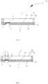
- Referring to
Fig. 1 , the present disclosure provides adisplay screen 100, including a light-shielding panel 10 and adisplay panel 20. The light-shielding panel 10 is provided with a hollow-out groove 11, and the hollow-outgroove 11 is configured to fasten afingerprint module 30 therein. Thedisplay panel 20 is superposed on a side of the light-shielding panel 10 towards a user. A side of thedisplay panel 20 towards the light-shielding panel 10 is provided with anink layer 21. An orthographic projection area of theink layer 21 on the light-shielding panel 10 coincides with the hollow-outgroove 11. Chromaticity of theink layer 21 is consistent with chromaticity of a side of the light-shielding panel 10 towards thedisplay panel 20. It could be understood that a visual effect when the user observes the light-shielding panel 10 through thedisplay panel 20 and a visual effect when the user observes theink layer 21 through thedisplay panel 20 are consistent, so that visual appearance is integrated when the user observes thedisplay screen 100 and the user experience is improved. Thedisplay screen 100 is applied to a mobile terminal, and the mobile terminal can be a mobile phone, a notebook computer, or a tablet computer. - With the
ink layer 21 being disposed at the side of thedisplay panel 20 towards the light-shielding panel 10 and the area of the orthographic projection of theink layer 21 on the light-shielding panel 10 coinciding with the hollow-outgroove 11, theink layer 21 is allowed to block thefingerprint module 30, and the chromaticity of theink layer 21 is consistent with the chromaticity of the side of the light-shielding panel 10 towards thedisplay panel 20, which reduces the color difference between theink layer 21 and the light-shielding panel 10 and improves the user experience. - The light-
shielding panel 10 is located at a back side of thedisplay panel 20. The light-shielding panel 10 blocks components at the back side for thedisplay panel 20 and prevents the user from seeing the components through thedisplay panel 20, so as to avoid an unclear display image of thedisplay panel 20. The light-shielding panel 10 includes afirst surface 12 towards thedisplay panel 20 and asecond surface 13 opposite thefirst surface 12. The hollow-outgroove 11 runs through from thefirst surface 12 to thesecond surface 13. Thefingerprint module 30 is fastened to the hollow-outgroove 11 so as to prevent the light-shielding panel 10 from blocking thefingerprint module 30 from sensing a user fingerprint, that is, it is convenient for thefingerprint module 30 to sense the user fingerprint through thedisplay panel 20. An area of the light-shieldingpanel 10 outside the hollow-outgroove 11 is lightproof, so that a display backdrop of thedisplay panel 20 can be formed at the area of the light-shieldingpanel 10 outside the hollow-outgroove 11, which is convenient for the user to view the display image of thedisplay panel 20. The hollow-outgroove 11 can be adjacent to a short edge of the light-shieldingpanel 10. In addition, when the user uses thedisplay screen 100 vertically, the hollow-outgroove 11 can be located at a bottom of the light-shieldingpanel 10, so as to make it convenient for thefingerprint module 30 in the hollow-outgroove 11 to acquire the user fingerprint. Certainly, in other embodiments, the light-shieldingpanel 10 can be provided with a plurality of hollow-outgrooves 11, and thefingerprint module 30 can be fastened to each of the hollow-outgrooves 11, so that the fingerprint recognition can be performed at a plurality of positions on thedisplay screen 100. - The
display panel 20 can display images, thedisplay panel 20 is provided with adisplay area 20a and anon-display area 20b adjacent to thedisplay area 20a. Thedisplay area 20a displays images. Thenon-display area 20b is provided with an encapsulation configuration and a circuit configuration. When thedisplay panel 20 does not display images, thedisplay area 20a can be pervious to light. An orthographic projection of the hollow-outgroove 11 on thedisplay panel 20 is located in thedisplay area 20a, that is, the user can input a fingerprint at a position of thedisplay screen 100 located in thedisplay area 20a. Thedisplay panel 20 includes anupper surface 23 and alower surface 24 opposite theupper surface 23. Theupper surface 23 faces the user, and thelower surface 24 is attached to thefirst surface 12 of the light-shieldingpanel 10. Theink layer 21 is coated on thelower surface 24. The user can see theink layer 21 through thedisplay panel 20, but cannot see thefingerprint module 30 through theink layer 21. The chromaticity of theink layer 21 is consistent with the chromaticity of thefirst surface 12 of the light-shieldingpanel 10, so that the color difference between theink layer 21 and thefirst surface 12 is reduced. The visual effects are integrated when user observes theink layer 21 and thefirst surface 12 through thedisplay panel 20. - Further, referring to
Fig. 2 , thefingerprint module 30 is an optical fingerprint module, theink layer 21 is provided with a plurality oftiny holes 211, and the plurality oftiny holes 211 are configured so that light of thefingerprint module 30 can be transmitted through the plurality oftiny holes 211. - The
fingerprint module 30 emits the light towards the user fingerprint, the light is reflected to thefingerprint module 30 by the user fingerprint after being received by the user fingerprint, and thefingerprint module 30 receives the reflected light. According to time difference between thefingerprint module 30 emitting the light and receiving the light, a distance from thefingerprint module 30 to the user fingerprint can be calculated, that is, a distance from thefingerprint module 30 to a peak or trough of the user fingerprint can be measured, so that the image of the user fingerprint can be obtained and the user fingerprint can be acquired. A plurality of beams of light can be transmitted through the plurality oftiny holes 211, that means multi-point acquisition of the user fingerprint is realized, and finally the user fingerprint image is conveniently formed. It could be understood that, the light emitted by thefingerprint module 30 can be transmitted through each of thetiny holes 211, or the light reflected back from the user fingerprint can be transmitted through each of thetiny holes 211, or not only the light emitted by thefingerprint module 30, but also the light reflected back from the user fingerprint can be transmitted through each of thetiny holes 211. Certainly, in other examples not covered by the claims, thefingerprint module 30 can also be a capacitive fingerprint module. - Further, the plurality of
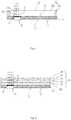
tiny holes 211 are arranged in an array. The hollow-outgroove 11 is formed to be a rectangular hole. Theink layer 21 is printed on thelower surface 24 of thedisplay panel 20 and opposite the hollow-outgroove 11. An area of theink layer 21 outside the plurality oftiny holes 211 is formed by screen printing, so that the plurality of thetiny holes 211 in the array are formed on theink layer 21. As the plurality oftiny holes 211 are arranged in the array, it is convenient to acquire the user fingerprint as arrayed point images, i.e. facilitating recording and recognition of the user fingerprint. Certainly, the plurality oftiny holes 211 can also be arranged at random. - Further, referring to
Fig. 3 , the plurality oftiny holes 211 includes a firsttiny hole 212 and a secondtiny hole 213, the firsttiny hole 212 is configured so that the light emitted by thefingerprint module 30 can be transmitted outside, and the secondtiny hole 213 is configured so that the light reflected from the outside can be transmitted towards thefingerprint module 30. - The
ink layer 21 is provided with a plurality pairs of the firsttiny hole 212 and the secondtiny hole 213. Each of the firsttiny holes 212 and each of the secondtiny holes 213 are adjacent to each other, and the light sent out through the firsttiny hole 212 and the reflected light through the secondtiny hole 213 are allowed to be independent from each other and have an improved distinguishing degree, so that the fingerprint acquisition efficiency is improved. - Further, the light-shielding
panel 10 is made from foam. The light-shieldingpanel 10 is bonded to thelower surface 24 of thedisplay panel 20 through an adhesive. The light-shieldingpanel 10 can protect thedisplay panel 20 effectively, prevent thedisplay panel 20 from being scratched or damaged, and can also avoid light leakage of thedisplay panel 20. Thefirst surface 12 of the light-shieldingpanel 10 appears black, the area of theink layer 21 outside thetiny holes 211 also appears black, and the chromaticity of thefirst surface 12 is consistent with the chromaticity of the area of theink layer 21 outside thetiny holes 211. Certainly, the light-shieldingpanel 10 can also be a plastic plate. - Further, referring to
Figs. 4 and5 , thedisplay panel 20 includes asubstrate 25 and adisplay layer 26, thesubstrate 25 is superposed on the light-shieldingpanel 10, and thedisplay layer 26 is superposed on a side of thesubstrate 25 away from the light-shieldingpanel 10. - As illustrated in
Fig. 4 , thedisplay panel 20 is a liquid crystal display panel. Thesubstrate 25 is a TFT (Thin Film Transistor) substrate, and thedisplay layer 26 is a liquid crystal layer. Thedisplay panel 20 further includes acolorful substrate 27 attached to a side of thedisplay layer 26 away from thesubstrate 25, anupper polarizer 28 attached to a side of thecolorful substrate 27 away from thedisplay layer 26, alower polarizer 29 attached to a side of thesubstrate 25 away from thedisplay layer 26, and abacklight source 20c attached to a side of thelower polarizer 29 away from thesubstrate 25. Theupper surface 23 is disposed to theupper polarizer 28, and thelower surface 24 is disposed to thebacklight source 20c. When thedisplay screen 100 does not display the images, thedisplay panel 20 can transmit the light of thefingerprint module 30 so as to realize the fingerprint acquisition. Certainly, when thedisplay screen 100 displays the images, thefingerprint module 30 emits the light having a different wave length from the light of thedisplay panel 20, and hence the fingerprint acquisition can be realized as well. - As illustrated in
Fig. 5 , thedisplay panel 20 is an OLED (Organic Light-Emitting Diode) display panel. Thesubstrate 25 is a glass substrate. Thedisplay layer 26 is an organic luminescent layer. Thedisplay panel 20 further includes ananode layer 227 attached between thedisplay layer 26 and thesubstrate 25, acathode layer 228 attached to a side of the display layer away from theanode layer 227, and anupper polarizer 229 attached to a side of thecathode layer 228 away from thedisplay layer 26. Theanode layer 227 and thecathode layer 228 drive thedisplay layer 26 to give out light. Theupper surface 23 is disposed to theupper polarizer 229, and thelower surface 24 is disposed to theanode layer 227. - Further, referring to
Fig. 6 , thedisplay screen 100 further includes a light-transparent cover plate 40, the light-transparent cover plate 40 is superposed on a side of thedisplay panel 20 away from the light-shieldingpanel 10, and the light-transparent cover plate 40 covers thedisplay panel 20. - The light-
transparent cover plate 40 is a glass plate. The light-transparent cover plate 40 and thedisplay panel 20 are bonded together through an optical adhesive. The light-transparent cover plate 40 protects thedisplay panel 20 from being scratched. When the finger of the user touches the light-transparent cover plate 40 and is corresponding to the position of the hollow-outgroove 11 of the light-shieldingpanel 10, thefingerprint module 30 acquires the fingerprint of the user's finger. - Referring to
Fig. 7 , the present disclosure further provides adisplay device 200. Thedisplay device 200 includes the above-mentioneddisplay screen 100 and further includes afingerprint module 30, thefingerprint module 30 being fastened to the hollow-outgroove 11. - The
fingerprint module 30 is fastened into the hollow-outgroove 11 and attached to theink layer 21. Thefingerprint module 30 includes abase 31, alight emitting source 32 and alight receiving source 33. Thebase 31 is a plate. A plurality of light emittingsources 32 is provided, and a plurality of light receivingsources 33 is provided. The plurality of thelight emitting source 32 and the plurality of thelight receiving source 33 are arrayed on the base 31 together. Each of thelight emitting sources 32 is corresponding to the firsttiny hole 212, and thelight receiving source 33 is corresponding to the secondtiny hole 213. Thelight emitting source 32 emits the light towards the user fingerprint through the firsttiny hole 212 and thedisplay panel 20, and thelight receiving source 33 receives the light reflected from the user fingerprint through thedisplay panel 20 and the secondtiny hole 213. - Referring to
Fig. 8 , the present disclosure further provides amobile terminal 300, and themobile terminal 300 includes the above-mentioneddisplay device 200 and further includes amain board 50 and aback casing 60. Thedisplay screen 100 and theback casing 60 are fitted together, themain board 50 is fastened between theback casing 60 and thedisplay screen 100, and thefingerprint module 30 is electrically connected to themain board 50 and transmits the acquired user fingerprint to themain board 50. It could be understood that themobile terminal 300 can be a mobile phone, a tablet computer, or a notebook computer and the like. - With the ink layer being disposed at the side of the display panel towards the light-shielding panel and the area of the orthographic projection of the ink layer on the light-shielding panel coinciding with the hollow-out groove, the ink layer is allowed to block the fingerprint module, and the chromaticity of the ink layer is consistent with the chromaticity of the side of the light-shielding panel towards the display panel, which reduces the color difference between the ink layer and the light-shielding panel and improves the user experience.
Claims (11)
- A display device, comprising a display screen (100) and an optical fingerprint module (30), the display screen (100) comprising a light-shielding panel (10) and a display panel (20), the light-shielding panel and the optical fingerprint module being located at a back side of the display panel, the light-shielding panel (10) being provided with a hollow-out groove (11), the optical fingerprint module (30) being fastened to the hollow-out groove (11), the display panel (20) being configured to be superposed on a side of the light-shielding panel (10) towards a user, a side of the display panel (20) towards the light-shielding panel (10) being provided with an ink layer (21), an orthographic projection area of the ink layer (21) on the light-shielding panel (10) coinciding with the hollow-out groove (11), and chromaticity of the ink layer (21) being consistent with chromaticity of a side of the light-shielding panel (10) towards the display panel (20);
wherein the light-shielding panel (10) comprises a first surface (12) towards the display panel (20) and a second surface (13) opposite the first surface (12), the hollow-out groove (11) runs through from the first surface (12) to the second surface (13),
wherein the ink layer (21) is provided with a plurality of tiny holes, and the plurality of tiny holes are configured so that light of the optical fingerprint module (30) can be transmitted;
wherein the plurality of tiny holes includes a first tiny hole (212) and a second tiny hole (213), the first tiny hole (212) is configured so that the light emitted by the optical fingerprint module (30) can be transmitted outside, and the second tiny hole (213) is configured so that the light reflected from the outside can be transmitted towards the optical fingerprint module (30). - The display device according to claim 1, wherein the light-shielding panel (10) is provided with a plurality of hollow-out grooves (11), and a plurality of the optical fingerprint modules (30) is fastened to the plurality of hollow-out grooves (11) respectively.
- The display device according to claim 1, wherein the plurality of tiny holes are arranged in an array.
- The display device according to any one of claims 1 to 3, wherein the light-shielding panel (10) is made from foam.
- The display device according to any one of claims 1 to 4, wherein the display panel (20) comprises a substrate (25) and a display layer (26), the substrate (25) is superposed on the light-shielding panel (10), and the display layer (26) is superposed on a side of the substrate (25) away from the light-shielding panel (10).
- The display device according to claim 5, wherein the display panel (20) is a liquid crystal display panel (20), the substrate (25) is a thin film transistor substrate (25), and the display layer (26) is a liquid crystal layer.
- The display device according to claim 6, wherein the display panel (20) further comprises a colorful substrate (27) attached to a side of the display layer (26) away from the substrate (25), an upper polarizer (28) attached to a side of the colorful substrate (27) away from the display layer (26), a lower polarizer (29) attached to a side of the substrate (25) away from the display layer (26), and a backlight source (20c) attached to a side of the lower polarizer (29) away from the substrate (25).
- The display device according to claim 5, wherein the display panel (20) is an organic light-emitting diode display panel (20), the substrate (25) is a glass substrate, and the display layer (26) is an organic luminescent layer.
- The display device according to any one of claims 1 to 8, wherein the display screen (100) further comprises a light-transparent cover plate (40), the light-transparent cover plate (40) is superposed on a side of the display panel (20) away from the light-shielding panel (10), and the light-transparent cover plate (40) covers the display panel (20).
- The display device according to any one of claims 1 to 9, wherein the optical fingerprint module (30) comprises a base (31), a light emitting source (32), and a light receiving source (33), the light emitting source (32) and the light receiving source (33) are both fastened to the base (31), the light emitting source (32) is configured to emit light to the outside through the display panel (20), and the light receiving source (33) is configured to receive the light reflected from the outside through the display panel (20).
- A mobile terminal, comprising a display device according to any one of claims 1 to 10.
Applications Claiming Priority (1)
| Application Number | Priority Date | Filing Date | Title |
|---|---|---|---|
| CN201710292547.7ACN107092311B (en) | 2017-04-27 | 2017-04-27 | Display screen, display device and mobile terminal |
Publications (2)
| Publication Number | Publication Date |
|---|---|
| EP3396588A1 EP3396588A1 (en) | 2018-10-31 |
| EP3396588B1true EP3396588B1 (en) | 2020-03-18 |
Family
ID=59638149
Family Applications (1)
| Application Number | Title | Priority Date | Filing Date |
|---|---|---|---|
| EP17210955.5AActiveEP3396588B1 (en) | 2017-04-27 | 2017-12-28 | Display screen, display device and mobile terminal |
Country Status (9)
| Country | Link |
|---|---|
| US (1) | US10520764B2 (en) |
| EP (1) | EP3396588B1 (en) |
| JP (1) | JP6884866B2 (en) |
| CN (1) | CN107092311B (en) |
| AU (1) | AU2018259305B2 (en) |
| ES (1) | ES2788669T3 (en) |
| SG (1) | SG11201906353RA (en) |
| TW (1) | TWI651658B (en) |
| WO (1) | WO2018196443A1 (en) |
Families Citing this family (30)
| Publication number | Priority date | Publication date | Assignee | Title |
|---|---|---|---|---|
| US9829614B2 (en)* | 2015-02-02 | 2017-11-28 | Synaptics Incorporated | Optical sensor using collimator |
| WO2017004328A1 (en)* | 2015-06-30 | 2017-01-05 | Bae Systems Controls Inc. | Vehicle display |
| KR101796660B1 (en) | 2016-04-19 | 2017-11-10 | 삼성전자주식회사 | Electronic device for supporting the fingerprint verification and operating method thereof |
| CN107025451B (en)* | 2017-04-27 | 2019-11-08 | 上海天马微电子有限公司 | A display panel and a display device |
| CN107092311B (en)* | 2017-04-27 | 2020-03-03 | Oppo广东移动通信有限公司 | Display screen, display device and mobile terminal |
| CN109934063B (en)* | 2017-12-18 | 2022-11-15 | 江西欧迈斯微电子有限公司 | Handheld terminal and fingerprint identification module thereof |
| CN111767892B (en)* | 2018-02-06 | 2021-10-22 | 深圳市汇顶科技股份有限公司 | Under-screen biometric identification device, biometric identification component and terminal equipment |
| KR102499978B1 (en)* | 2018-02-12 | 2023-02-15 | 삼성디스플레이 주식회사 | Display device |
| KR102608694B1 (en)* | 2018-04-18 | 2023-12-04 | 삼성전자 주식회사 | Electronic device comprising phase retarder and polarizing element for blocking out light reflected by sensor disposed below display thereof |
| CN109313703B (en) | 2018-08-15 | 2022-02-08 | 深圳市汇顶科技股份有限公司 | Optical fingerprint identification system under screen, backlight module, display screen and electronic equipment |
| WO2020037683A1 (en) | 2018-08-24 | 2020-02-27 | 深圳市汇顶科技股份有限公司 | Backlight module, below-screen fingerprint recognition method and apparatus, and electronic device |
| WO2020056544A1 (en)* | 2018-09-17 | 2020-03-26 | 深圳市汇顶科技股份有限公司 | Under-screen optical detection system, electronic device and object proximity detection method therefor |
| CN109446908A (en)* | 2018-09-27 | 2019-03-08 | 维沃移动通信有限公司 | A kind of mobile terminal |
| CN109040380B (en)* | 2018-09-29 | 2024-11-01 | 西安易朴通讯技术有限公司 | Display device and mobile terminal |
| CN109002229B (en)* | 2018-10-15 | 2021-06-18 | 上海天马微电子有限公司 | Touch panel, display module and touch display device |
| CN109215604B (en)* | 2018-11-07 | 2021-01-26 | 京东方科技集团股份有限公司 | Display device and texture recognition method thereof, product implementing the method, and texture recognition device |
| CN110648586B (en)* | 2018-11-21 | 2022-04-01 | Oppo广东移动通信有限公司 | an electronic device |
| CN211180476U (en) | 2018-12-07 | 2020-08-04 | 鸿富锦精密工业(深圳)有限公司 | Liquid crystal display device |
| CN211454161U (en) | 2018-12-07 | 2020-09-08 | 鸿富锦精密工业(深圳)有限公司 | Liquid crystal display device having a plurality of pixel electrodes |
| CN111310513A (en)* | 2018-12-11 | 2020-06-19 | 上海耕岩智能科技有限公司 | Biological feature recognition structure, system and method under coding mask type screen |
| CN111510522B (en)* | 2019-01-31 | 2022-05-06 | 北京小米移动软件有限公司 | Screen Bezels, Display Modules and Terminals |
| KR102782192B1 (en)* | 2019-05-09 | 2025-03-17 | 삼성전자주식회사 | An electronic device including a display module including a sensor and a method of manufacturing the display module |
| CN110321876B (en)* | 2019-07-24 | 2021-05-25 | 维沃移动通信有限公司 | Capacitance fingerprint identification module and terminal equipment |
| KR20210044943A (en)* | 2019-10-15 | 2021-04-26 | 삼성디스플레이 주식회사 | display apparatus and method manufacturing the same |
| JP7408415B2 (en)* | 2020-01-27 | 2024-01-05 | 株式会社ジャパンディスプレイ | Electronics |
| KR20210109091A (en)* | 2020-02-26 | 2021-09-06 | 삼성디스플레이 주식회사 | Electronic apparatus |
| CN111524451B (en)* | 2020-04-30 | 2022-03-22 | 昆山国显光电有限公司 | Display panel and display device |
| CN111754875B (en)* | 2020-06-28 | 2022-04-19 | 合肥维信诺科技有限公司 | Display module and display device |
| US12271238B2 (en) | 2022-06-16 | 2025-04-08 | Chicony Power Technology Co., Ltd. | Illuminated touch module having light guide plate |
| CN116156812A (en)* | 2023-01-17 | 2023-05-23 | 苏州胜利精密制造科技股份有限公司 | Integrated black cover plate structure and preparation method thereof |
Citations (2)
| Publication number | Priority date | Publication date | Assignee | Title |
|---|---|---|---|---|
| US6327376B1 (en)* | 1997-12-04 | 2001-12-04 | U.S. Philips Corporation | Electronic apparatus comprising fingerprint sensing devices |
| CN106412166A (en)* | 2016-11-23 | 2017-02-15 | 广东欧珀移动通信有限公司 | Terminal and casing assembly thereof |
Family Cites Families (30)
| Publication number | Priority date | Publication date | Assignee | Title |
|---|---|---|---|---|
| FR2857482B1 (en)* | 2003-07-09 | 2005-10-21 | Groupe Ecoles Telecomm | OPTICAL IMAGING DEVICE, IN PARTICULAR FOR THE RECOGNITION OF DIGITAL IMPRESSIONS |
| JP2008205317A (en)* | 2007-02-21 | 2008-09-04 | Nec Electronics Corp | Solid-state imaging device, manufacturing method thereof, and electronic apparatus using the same |
| US8605960B2 (en) | 2009-03-02 | 2013-12-10 | Avago Technologies General Ip (Singapore) Pte. Ltd. | Fingerprint sensing device |
| US9013613B2 (en)* | 2010-09-21 | 2015-04-21 | Sony Corporation | Sensor-equipped display apparatus and electronic apparatus |
| US8467177B2 (en)* | 2010-10-29 | 2013-06-18 | Apple Inc. | Displays with polarizer windows and opaque masking layers for electronic devices |
| US9891098B2 (en)* | 2010-12-30 | 2018-02-13 | Apple Inc. | Diffuser and filter structures for light sensors |
| JP5202654B2 (en)* | 2011-01-14 | 2013-06-05 | 株式会社ナナオ | Sensor unit operation mechanism |
| JP5427228B2 (en)* | 2011-12-13 | 2014-02-26 | シャープ株式会社 | Display device and television receiver |
| US9836165B2 (en) | 2014-05-16 | 2017-12-05 | Apple Inc. | Integrated silicon-OLED display and touch sensor panel |
| CN104182727B (en)* | 2014-05-16 | 2021-07-30 | 深圳印象认知技术有限公司 | Ultra-thin fingerprint and palm print acquisition device and fingerprint and palm print image acquisition method |
| CN106203412A (en) | 2015-01-16 | 2016-12-07 | 宁波舜宇光电信息有限公司 | Optical imaging device and manufacture method thereof and application |
| US10147757B2 (en)* | 2015-02-02 | 2018-12-04 | Synaptics Incorporated | Image sensor structures for fingerprint sensing |
| TWM506323U (en)* | 2015-02-03 | 2015-08-01 | Tpk Touch Solutions Xiamen Inc | Touch control device |
| KR102272470B1 (en)* | 2015-03-18 | 2021-07-05 | 삼성디스플레이 주식회사 | Display device |
| CN105528568B (en)* | 2015-06-19 | 2017-07-07 | 宸鸿科技(厦门)有限公司 | Fingeprint distinguisher and its manufacture method |
| KR102374479B1 (en)* | 2015-08-13 | 2022-03-16 | 삼성전자주식회사 | Electronic device having display and sensor |
| CN105184248B (en) | 2015-08-28 | 2019-03-12 | 京东方科技集团股份有限公司 | A fingerprint identification device and fingerprint identification system |
| KR102524754B1 (en)* | 2015-09-09 | 2023-04-21 | 엘지디스플레이 주식회사 | Display device |
| CN204990245U (en) | 2015-09-23 | 2016-01-20 | 维沃移动通信有限公司 | Touch -sensitive screen, touch -sensitive screen integrated configuration and electronic equipment |
| CN205015864U (en) | 2015-09-30 | 2016-02-03 | 深圳欧菲光科技股份有限公司 | Touch screen |
| CN106569358A (en)* | 2015-10-09 | 2017-04-19 | 小米科技有限责任公司 | Liquid crystal display components and electronic equipment |
| US9710689B2 (en)* | 2015-10-30 | 2017-07-18 | Essential Products, Inc. | Fingerprint sensors for mobile devices |
| CN105678255B (en)* | 2016-01-04 | 2019-01-08 | 京东方科技集团股份有限公司 | A kind of optical fingerprint identification display screen and display device |
| CN105872137B (en)* | 2016-03-25 | 2017-10-27 | 广东欧珀移动通信有限公司 | Display screen component and the mobile terminal with it |
| CN107451513B (en)* | 2016-05-31 | 2023-12-29 | 宸鸿科技(厦门)有限公司 | Fingerprint identification device |
| CN106228144B (en) | 2016-08-02 | 2023-10-13 | 京东方科技集团股份有限公司 | Fingerprint identification display device |
| CN106096595B (en) | 2016-08-08 | 2022-08-09 | 京东方科技集团股份有限公司 | Fingerprint identification module, manufacturing method thereof and fingerprint identification display device |
| CN106503635B (en)* | 2016-10-11 | 2019-06-28 | Oppo广东移动通信有限公司 | Cover plate for optical fingerprint identification, input assembly and electronic device |
| CN106385473B (en) | 2016-10-29 | 2022-09-09 | Oppo广东移动通信有限公司 | Housing, fingerprint module and mobile terminal |
| CN107092311B (en) | 2017-04-27 | 2020-03-03 | Oppo广东移动通信有限公司 | Display screen, display device and mobile terminal |
- 2017
- 2017-04-27CNCN201710292547.7Apatent/CN107092311B/enactiveActive
- 2017-12-13TWTW106143734Apatent/TWI651658B/enactive
- 2017-12-27USUS15/854,956patent/US10520764B2/enactiveActive
- 2017-12-28ESES17210955Tpatent/ES2788669T3/enactiveActive
- 2017-12-28EPEP17210955.5Apatent/EP3396588B1/enactiveActive
- 2018
- 2018-01-04SGSG11201906353RApatent/SG11201906353RA/enunknown
- 2018-01-04WOPCT/CN2018/071316patent/WO2018196443A1/ennot_activeCeased
- 2018-01-04JPJP2019534724Apatent/JP6884866B2/enactiveActive
- 2018-01-04AUAU2018259305Apatent/AU2018259305B2/ennot_activeCeased
Patent Citations (2)
| Publication number | Priority date | Publication date | Assignee | Title |
|---|---|---|---|---|
| US6327376B1 (en)* | 1997-12-04 | 2001-12-04 | U.S. Philips Corporation | Electronic apparatus comprising fingerprint sensing devices |
| CN106412166A (en)* | 2016-11-23 | 2017-02-15 | 广东欧珀移动通信有限公司 | Terminal and casing assembly thereof |
Also Published As
| Publication number | Publication date |
|---|---|
| AU2018259305B2 (en) | 2020-05-21 |
| AU2018259305A1 (en) | 2019-07-25 |
| US10520764B2 (en) | 2019-12-31 |
| ES2788669T3 (en) | 2020-10-22 |
| WO2018196443A1 (en) | 2018-11-01 |
| SG11201906353RA (en) | 2019-08-27 |
| CN107092311B (en) | 2020-03-03 |
| TWI651658B (en) | 2019-02-21 |
| JP2020507104A (en) | 2020-03-05 |
| TW201839656A (en) | 2018-11-01 |
| US20180314096A1 (en) | 2018-11-01 |
| JP6884866B2 (en) | 2021-06-09 |
| EP3396588A1 (en) | 2018-10-31 |
| CN107092311A (en) | 2017-08-25 |
Similar Documents
| Publication | Publication Date | Title |
|---|---|---|
| EP3396588B1 (en) | Display screen, display device and mobile terminal | |
| CN109496313B (en) | Fingerprint identification device and electronic equipment | |
| CN110770746B (en) | Fingerprint identification device and electronic equipment | |
| CN107092310B (en) | Display screen, display device and mobile terminal | |
| JP2018097871A (en) | Flat panel display with built-in optical image recognition sensor | |
| WO2020082375A1 (en) | Compound lens structure, fingerprint recognition apparatus, and electronic device | |
| US11816295B2 (en) | Electronic devices having moisture-insensitive optical touch sensors | |
| KR102460111B1 (en) | Flat Panel Display Embedding Optical Imaging Sensor | |
| CN210605736U (en) | Fingerprint detection device, display screen and electronic equipment | |
| CN111586267A (en) | Optical sensing devices and electronic equipment | |
| CN212163464U (en) | Optical sensing devices and electronic equipment | |
| CN212163466U (en) | Optical sensing devices and electronic equipment | |
| CN111464727A (en) | Optical sensing device and electronic apparatus | |
| CN209297320U (en) | Fingerprint identification device and electronic equipment | |
| JP2022535172A (en) | terminal equipment | |
| US20230341975A1 (en) | Electronic Devices Having Moisture-Insensitive Optical Touch Sensors | |
| CN111095271B (en) | Fingerprint detection devices, displays and electronic equipment | |
| CN111464726A (en) | Optical sensing devices and electronic equipment | |
| KR102440209B1 (en) | Flat Panel Display Embedding Optical Imaging Sensor | |
| HK1237915A (en) | Display screen, display device and mobile terminal | |
| HK1237915A1 (en) | Display screen, display device and mobile terminal | |
| HK1237915B (en) | Display screen, display device and mobile terminal |
Legal Events
| Date | Code | Title | Description |
|---|---|---|---|
| PUAI | Public reference made under article 153(3) epc to a published international application that has entered the european phase | Free format text:ORIGINAL CODE: 0009012 | |
| STAA | Information on the status of an ep patent application or granted ep patent | Free format text:STATUS: REQUEST FOR EXAMINATION WAS MADE | |
| 17P | Request for examination filed | Effective date:20180822 | |
| AK | Designated contracting states | Kind code of ref document:A1 Designated state(s):AL AT BE BG CH CY CZ DE DK EE ES FI FR GB GR HR HU IE IS IT LI LT LU LV MC MK MT NL NO PL PT RO RS SE SI SK SM TR | |
| AX | Request for extension of the european patent | Extension state:BA ME | |
| STAA | Information on the status of an ep patent application or granted ep patent | Free format text:STATUS: EXAMINATION IS IN PROGRESS | |
| 17Q | First examination report despatched | Effective date:20190205 | |
| GRAP | Despatch of communication of intention to grant a patent | Free format text:ORIGINAL CODE: EPIDOSNIGR1 | |
| RAP1 | Party data changed (applicant data changed or rights of an application transferred) | Owner name:GUANGDONG OPPO MOBILE TELECOMMUNICATIONS CORP., LT | |
| STAA | Information on the status of an ep patent application or granted ep patent | Free format text:STATUS: GRANT OF PATENT IS INTENDED | |
| INTG | Intention to grant announced | Effective date:20191212 | |
| GRAS | Grant fee paid | Free format text:ORIGINAL CODE: EPIDOSNIGR3 | |
| GRAA | (expected) grant | Free format text:ORIGINAL CODE: 0009210 | |
| STAA | Information on the status of an ep patent application or granted ep patent | Free format text:STATUS: THE PATENT HAS BEEN GRANTED | |
| AK | Designated contracting states | Kind code of ref document:B1 Designated state(s):AL AT BE BG CH CY CZ DE DK EE ES FI FR GB GR HR HU IE IS IT LI LT LU LV MC MK MT NL NO PL PT RO RS SE SI SK SM TR | |
| REG | Reference to a national code | Ref country code:GB Ref legal event code:FG4D | |
| REG | Reference to a national code | Ref country code:DE Ref legal event code:R096 Ref document number:602017013226 Country of ref document:DE | |
| REG | Reference to a national code | Ref country code:AT Ref legal event code:REF Ref document number:1246783 Country of ref document:AT Kind code of ref document:T Effective date:20200415 Ref country code:IE Ref legal event code:FG4D | |
| REG | Reference to a national code | Ref country code:NL Ref legal event code:FP | |
| PG25 | Lapsed in a contracting state [announced via postgrant information from national office to epo] | Ref country code:RS Free format text:LAPSE BECAUSE OF FAILURE TO SUBMIT A TRANSLATION OF THE DESCRIPTION OR TO PAY THE FEE WITHIN THE PRESCRIBED TIME-LIMIT Effective date:20200318 Ref country code:FI Free format text:LAPSE BECAUSE OF FAILURE TO SUBMIT A TRANSLATION OF THE DESCRIPTION OR TO PAY THE FEE WITHIN THE PRESCRIBED TIME-LIMIT Effective date:20200318 Ref country code:NO Free format text:LAPSE BECAUSE OF FAILURE TO SUBMIT A TRANSLATION OF THE DESCRIPTION OR TO PAY THE FEE WITHIN THE PRESCRIBED TIME-LIMIT Effective date:20200618 | |
| PG25 | Lapsed in a contracting state [announced via postgrant information from national office to epo] | Ref country code:HR Free format text:LAPSE BECAUSE OF FAILURE TO SUBMIT A TRANSLATION OF THE DESCRIPTION OR TO PAY THE FEE WITHIN THE PRESCRIBED TIME-LIMIT Effective date:20200318 Ref country code:LV Free format text:LAPSE BECAUSE OF FAILURE TO SUBMIT A TRANSLATION OF THE DESCRIPTION OR TO PAY THE FEE WITHIN THE PRESCRIBED TIME-LIMIT Effective date:20200318 Ref country code:SE Free format text:LAPSE BECAUSE OF FAILURE TO SUBMIT A TRANSLATION OF THE DESCRIPTION OR TO PAY THE FEE WITHIN THE PRESCRIBED TIME-LIMIT Effective date:20200318 Ref country code:BG Free format text:LAPSE BECAUSE OF FAILURE TO SUBMIT A TRANSLATION OF THE DESCRIPTION OR TO PAY THE FEE WITHIN THE PRESCRIBED TIME-LIMIT Effective date:20200618 Ref country code:GR Free format text:LAPSE BECAUSE OF FAILURE TO SUBMIT A TRANSLATION OF THE DESCRIPTION OR TO PAY THE FEE WITHIN THE PRESCRIBED TIME-LIMIT Effective date:20200619 | |
| REG | Reference to a national code | Ref country code:LT Ref legal event code:MG4D | |
| REG | Reference to a national code | Ref country code:ES Ref legal event code:FG2A Ref document number:2788669 Country of ref document:ES Kind code of ref document:T3 Effective date:20201022 | |
| PG25 | Lapsed in a contracting state [announced via postgrant information from national office to epo] | Ref country code:LT Free format text:LAPSE BECAUSE OF FAILURE TO SUBMIT A TRANSLATION OF THE DESCRIPTION OR TO PAY THE FEE WITHIN THE PRESCRIBED TIME-LIMIT Effective date:20200318 Ref country code:RO Free format text:LAPSE BECAUSE OF FAILURE TO SUBMIT A TRANSLATION OF THE DESCRIPTION OR TO PAY THE FEE WITHIN THE PRESCRIBED TIME-LIMIT Effective date:20200318 Ref country code:CZ Free format text:LAPSE BECAUSE OF FAILURE TO SUBMIT A TRANSLATION OF THE DESCRIPTION OR TO PAY THE FEE WITHIN THE PRESCRIBED TIME-LIMIT Effective date:20200318 Ref country code:PT Free format text:LAPSE BECAUSE OF FAILURE TO SUBMIT A TRANSLATION OF THE DESCRIPTION OR TO PAY THE FEE WITHIN THE PRESCRIBED TIME-LIMIT Effective date:20200812 Ref country code:EE Free format text:LAPSE BECAUSE OF FAILURE TO SUBMIT A TRANSLATION OF THE DESCRIPTION OR TO PAY THE FEE WITHIN THE PRESCRIBED TIME-LIMIT Effective date:20200318 Ref country code:SK Free format text:LAPSE BECAUSE OF FAILURE TO SUBMIT A TRANSLATION OF THE DESCRIPTION OR TO PAY THE FEE WITHIN THE PRESCRIBED TIME-LIMIT Effective date:20200318 Ref country code:SM Free format text:LAPSE BECAUSE OF FAILURE TO SUBMIT A TRANSLATION OF THE DESCRIPTION OR TO PAY THE FEE WITHIN THE PRESCRIBED TIME-LIMIT Effective date:20200318 Ref country code:IS Free format text:LAPSE BECAUSE OF FAILURE TO SUBMIT A TRANSLATION OF THE DESCRIPTION OR TO PAY THE FEE WITHIN THE PRESCRIBED TIME-LIMIT Effective date:20200718 | |
| REG | Reference to a national code | Ref country code:AT Ref legal event code:MK05 Ref document number:1246783 Country of ref document:AT Kind code of ref document:T Effective date:20200318 | |
| REG | Reference to a national code | Ref country code:DE Ref legal event code:R097 Ref document number:602017013226 Country of ref document:DE | |
| PLBE | No opposition filed within time limit | Free format text:ORIGINAL CODE: 0009261 | |
| STAA | Information on the status of an ep patent application or granted ep patent | Free format text:STATUS: NO OPPOSITION FILED WITHIN TIME LIMIT | |
| PG25 | Lapsed in a contracting state [announced via postgrant information from national office to epo] | Ref country code:DK Free format text:LAPSE BECAUSE OF FAILURE TO SUBMIT A TRANSLATION OF THE DESCRIPTION OR TO PAY THE FEE WITHIN THE PRESCRIBED TIME-LIMIT Effective date:20200318 Ref country code:AT Free format text:LAPSE BECAUSE OF FAILURE TO SUBMIT A TRANSLATION OF THE DESCRIPTION OR TO PAY THE FEE WITHIN THE PRESCRIBED TIME-LIMIT Effective date:20200318 | |
| 26N | No opposition filed | Effective date:20201221 | |
| PG25 | Lapsed in a contracting state [announced via postgrant information from national office to epo] | Ref country code:PL Free format text:LAPSE BECAUSE OF FAILURE TO SUBMIT A TRANSLATION OF THE DESCRIPTION OR TO PAY THE FEE WITHIN THE PRESCRIBED TIME-LIMIT Effective date:20200318 | |
| PG25 | Lapsed in a contracting state [announced via postgrant information from national office to epo] | Ref country code:SI Free format text:LAPSE BECAUSE OF FAILURE TO SUBMIT A TRANSLATION OF THE DESCRIPTION OR TO PAY THE FEE WITHIN THE PRESCRIBED TIME-LIMIT Effective date:20200318 | |
| REG | Reference to a national code | Ref country code:CH Ref legal event code:PL | |
| PG25 | Lapsed in a contracting state [announced via postgrant information from national office to epo] | Ref country code:MC Free format text:LAPSE BECAUSE OF FAILURE TO SUBMIT A TRANSLATION OF THE DESCRIPTION OR TO PAY THE FEE WITHIN THE PRESCRIBED TIME-LIMIT Effective date:20200318 | |
| REG | Reference to a national code | Ref country code:BE Ref legal event code:MM Effective date:20201231 | |
| PG25 | Lapsed in a contracting state [announced via postgrant information from national office to epo] | Ref country code:LU Free format text:LAPSE BECAUSE OF NON-PAYMENT OF DUE FEES Effective date:20201228 Ref country code:IE Free format text:LAPSE BECAUSE OF NON-PAYMENT OF DUE FEES Effective date:20201228 | |
| REG | Reference to a national code | Ref country code:DE Ref legal event code:R079 Ref document number:602017013226 Country of ref document:DE Free format text:PREVIOUS MAIN CLASS: G06K0009000000 Ipc:G06V0010000000 | |
| PG25 | Lapsed in a contracting state [announced via postgrant information from national office to epo] | Ref country code:LI Free format text:LAPSE BECAUSE OF NON-PAYMENT OF DUE FEES Effective date:20201231 Ref country code:CH Free format text:LAPSE BECAUSE OF NON-PAYMENT OF DUE FEES Effective date:20201231 | |
| PG25 | Lapsed in a contracting state [announced via postgrant information from national office to epo] | Ref country code:TR Free format text:LAPSE BECAUSE OF FAILURE TO SUBMIT A TRANSLATION OF THE DESCRIPTION OR TO PAY THE FEE WITHIN THE PRESCRIBED TIME-LIMIT Effective date:20200318 Ref country code:MT Free format text:LAPSE BECAUSE OF FAILURE TO SUBMIT A TRANSLATION OF THE DESCRIPTION OR TO PAY THE FEE WITHIN THE PRESCRIBED TIME-LIMIT Effective date:20200318 Ref country code:CY Free format text:LAPSE BECAUSE OF FAILURE TO SUBMIT A TRANSLATION OF THE DESCRIPTION OR TO PAY THE FEE WITHIN THE PRESCRIBED TIME-LIMIT Effective date:20200318 | |
| PG25 | Lapsed in a contracting state [announced via postgrant information from national office to epo] | Ref country code:MK Free format text:LAPSE BECAUSE OF FAILURE TO SUBMIT A TRANSLATION OF THE DESCRIPTION OR TO PAY THE FEE WITHIN THE PRESCRIBED TIME-LIMIT Effective date:20200318 Ref country code:AL Free format text:LAPSE BECAUSE OF FAILURE TO SUBMIT A TRANSLATION OF THE DESCRIPTION OR TO PAY THE FEE WITHIN THE PRESCRIBED TIME-LIMIT Effective date:20200318 | |
| PG25 | Lapsed in a contracting state [announced via postgrant information from national office to epo] | Ref country code:BE Free format text:LAPSE BECAUSE OF NON-PAYMENT OF DUE FEES Effective date:20201231 | |
| P01 | Opt-out of the competence of the unified patent court (upc) registered | Effective date:20230412 | |
| PGFP | Annual fee paid to national office [announced via postgrant information from national office to epo] | Ref country code:NL Payment date:20241127 Year of fee payment:8 | |
| PGFP | Annual fee paid to national office [announced via postgrant information from national office to epo] | Ref country code:DE Payment date:20241216 Year of fee payment:8 | |
| PGFP | Annual fee paid to national office [announced via postgrant information from national office to epo] | Ref country code:GB Payment date:20241213 Year of fee payment:8 | |
| PGFP | Annual fee paid to national office [announced via postgrant information from national office to epo] | Ref country code:FR Payment date:20241216 Year of fee payment:8 | |
| PGFP | Annual fee paid to national office [announced via postgrant information from national office to epo] | Ref country code:IT Payment date:20241211 Year of fee payment:8 | |
| PGFP | Annual fee paid to national office [announced via postgrant information from national office to epo] | Ref country code:ES Payment date:20250107 Year of fee payment:8 |