EP3391459B1 - Time delay filters - Google Patents
Time delay filtersDownload PDFInfo
- Publication number
- EP3391459B1 EP3391459B1EP16876852.1AEP16876852AEP3391459B1EP 3391459 B1EP3391459 B1EP 3391459B1EP 16876852 AEP16876852 AEP 16876852AEP 3391459 B1EP3391459 B1EP 3391459B1
- Authority
- EP
- European Patent Office
- Prior art keywords
- time delay
- resonator
- conductive
- delay filter
- coupled
- Prior art date
- Legal status (The legal status is an assumption and is not a legal conclusion. Google has not performed a legal analysis and makes no representation as to the accuracy of the status listed.)
- Active
Links
Images


Classifications
- H—ELECTRICITY
- H03—ELECTRONIC CIRCUITRY
- H03H—IMPEDANCE NETWORKS, e.g. RESONANT CIRCUITS; RESONATORS
- H03H7/00—Multiple-port networks comprising only passive electrical elements as network components
- H03H7/30—Time-delay networks
- H03H7/32—Time-delay networks with lumped inductance and capacitance
- H—ELECTRICITY
- H03—ELECTRONIC CIRCUITRY
- H03H—IMPEDANCE NETWORKS, e.g. RESONANT CIRCUITS; RESONATORS
- H03H7/00—Multiple-port networks comprising only passive electrical elements as network components
- H03H7/01—Frequency selective two-port networks
- H03H7/0115—Frequency selective two-port networks comprising only inductors and capacitors
- H—ELECTRICITY
- H03—ELECTRONIC CIRCUITRY
- H03H—IMPEDANCE NETWORKS, e.g. RESONANT CIRCUITS; RESONATORS
- H03H7/00—Multiple-port networks comprising only passive electrical elements as network components
- H03H7/01—Frequency selective two-port networks
- H03H7/09—Filters comprising mutual inductance
- H—ELECTRICITY
- H03—ELECTRONIC CIRCUITRY
- H03H—IMPEDANCE NETWORKS, e.g. RESONANT CIRCUITS; RESONATORS
- H03H7/00—Multiple-port networks comprising only passive electrical elements as network components
- H03H7/01—Frequency selective two-port networks
- H03H7/17—Structural details of sub-circuits of frequency selective networks
- H03H7/1708—Comprising bridging elements, i.e. elements in a series path without own reference to ground and spanning branching nodes of another series path
- H—ELECTRICITY
- H03—ELECTRONIC CIRCUITRY
- H03H—IMPEDANCE NETWORKS, e.g. RESONANT CIRCUITS; RESONATORS
- H03H7/00—Multiple-port networks comprising only passive electrical elements as network components
- H03H7/01—Frequency selective two-port networks
- H03H7/17—Structural details of sub-circuits of frequency selective networks
- H03H7/1741—Comprising typical LC combinations, irrespective of presence and location of additional resistors
- H03H7/1775—Parallel LC in shunt or branch path
- H—ELECTRICITY
- H03—ELECTRONIC CIRCUITRY
- H03H—IMPEDANCE NETWORKS, e.g. RESONANT CIRCUITS; RESONATORS
- H03H7/00—Multiple-port networks comprising only passive electrical elements as network components
- H03H7/30—Time-delay networks
- H03H7/32—Time-delay networks with lumped inductance and capacitance
- H03H7/325—Adjustable networks
- H—ELECTRICITY
- H03—ELECTRONIC CIRCUITRY
- H03H—IMPEDANCE NETWORKS, e.g. RESONANT CIRCUITS; RESONATORS
- H03H7/00—Multiple-port networks comprising only passive electrical elements as network components
- H03H7/30—Time-delay networks
- H03H7/34—Time-delay networks with lumped and distributed reactance
- H03H7/345—Adjustable networks
- H—ELECTRICITY
- H01—ELECTRIC ELEMENTS
- H01L—SEMICONDUCTOR DEVICES NOT COVERED BY CLASS H10
- H01L2224/00—Indexing scheme for arrangements for connecting or disconnecting semiconductor or solid-state bodies and methods related thereto as covered by H01L24/00
- H01L2224/01—Means for bonding being attached to, or being formed on, the surface to be connected, e.g. chip-to-package, die-attach, "first-level" interconnects; Manufacturing methods related thereto
- H01L2224/42—Wire connectors; Manufacturing methods related thereto
- H01L2224/47—Structure, shape, material or disposition of the wire connectors after the connecting process
- H01L2224/48—Structure, shape, material or disposition of the wire connectors after the connecting process of an individual wire connector
- H01L2224/481—Disposition
- H01L2224/48151—Connecting between a semiconductor or solid-state body and an item not being a semiconductor or solid-state body, e.g. chip-to-substrate, chip-to-passive
- H01L2224/48153—Connecting between a semiconductor or solid-state body and an item not being a semiconductor or solid-state body, e.g. chip-to-substrate, chip-to-passive the body and the item being arranged next to each other, e.g. on a common substrate
- H01L2224/48195—Connecting between a semiconductor or solid-state body and an item not being a semiconductor or solid-state body, e.g. chip-to-substrate, chip-to-passive the body and the item being arranged next to each other, e.g. on a common substrate the item being a discrete passive component
- H—ELECTRICITY
- H03—ELECTRONIC CIRCUITRY
- H03H—IMPEDANCE NETWORKS, e.g. RESONANT CIRCUITS; RESONATORS
- H03H1/00—Constructional details of impedance networks whose electrical mode of operation is not specified or applicable to more than one type of network
- H03H2001/0021—Constructional details
- H03H2001/0085—Multilayer, e.g. LTCC, HTCC, green sheets
Definitions
- This inventionrelates to time delay filters.
- Time delay elementsare used in a variety of analog circuits to cause analog signals to experience a time delay.
- time delay elementsare particularly important for RF transceivers, where they may be used for amplifier pre-distortion, feed-forward linearization, and active interference cancellation techniques.
- time delay elementsmay find use in a wide variety of applications involving analog signal transmission, processing, and/or synthesis.
- the systems described hereinmay increase performance of full-duplex transceivers (and other applicable systems) by enabling high accuracy time delay filtering without prohibitive increases in circuit complexity and/or cost.
- Other applicable systemsinclude active sensing systems (e.g., RADAR), wired communications systems, wireless communications systems, channel emulators, reflectometers, PIM analyzers and/or any other suitable system, including communication systems where transmit and receive bands are close in frequency, but not overlapping.
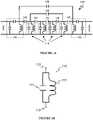
- a time delay filter 100includes one or more LC resonators 110.
- the time delay filter 100may additionally include intra-filter coupling elements 120 and/or input matching elements 130.
- the time delay filter 100may additionally or alternatively include any number of LC resonators 110 (e.g., the set of LC resonators 110 may contain only a single LC resonator).
- the time delay filter 100may additionally or alternatively include any suitable components coupled to the LC resonator(s) 110 that aid or otherwise contribute the production of a time delay, such as passive or active components (e.g., capacitors, transistors, switches, etc.), integrated components (e.g., conductive layers and/or traces), or any other suitable components.
- the time delay filter 100preferably functions to produce a substantially frequency-invariant group delay for analog signals within a particular frequency band of interest; typically a frequency band within the range of radio frequencies (RF), but alternatively any suitable frequency band in any suitable frequency range.
- a group delay of an analog signalwill delay the amplitude envelope of each frequency component of the signal; a frequency-invariant group delay will apply an equal time delay to the amplitude envelope of each frequency component of the signal.
- the time delay filter 100can additionally or alternatively function to increase the performance of signal transceivers (or other applicable systems; e.g., phased antenna arrays) by enabling high accuracy, adjustable, and/or reconfigurable group delay of signals without prohibitive increases in circuit complexity and/or cost.
- the time delay filter 100preferably has a relatively low and frequency-invariant (in a frequency band of interest) insertion loss (e.g., 1 dB, 3 dB, or 5 dB of insertion loss and/or attenuation).
- the magnitude of the frequency response of the time delay filter 100is substantially flat over the range of frequencies of interest (e.g., over the range of radio frequencies) and has a magnitude ripple that is small relative to the signal magnitude (e.g., 10 ⁇ , 100 ⁇ , or 1000 ⁇ smaller).
- the time delay filter 100may have any suitable insertion loss, that varies with frequency in any suitable manner.
- the time delay filter 100preferably is constructed from lumped and/or distributed inductors and capacitors that are integrated into the substrate of a laminate (e.g., a printed circuit board), of a microchip (e.g., a silicon substrate), or any other suitable circuit substrate. Integration of the time delay filter 100 may substantially reduce cost and size of the time delay filter 100.
- Portions of the time delay filtermay additionally or alternatively be added to the substrate as discrete components.
- the LC resonator(s) 110 of the time delay filter 100may be integrated into the substrate, and input matching element(s) 130 and/or intra-filter coupling element(s) 120 may be coupled to the substrate and/or the LC resonators as discrete components (e.g., via wire bonding, surface mounting, etc.).
- the time delay filter 100is preferably implemented using analog circuitry, but additionally or alternatively may be implemented by digital circuitry or any combination of analog and digital circuitry.
- Analog circuitryis preferably implemented using a combination of the circuit substrate and metallized/conductive layers as described above, but can additionally or alternatively be implemented using analog integrated circuits (ICs) and/or discrete components (e.g., capacitors, inductors, resistors, transistors), wires, transmission lines, transformers, couplers, hybrids, waveguides, digital components, mixed-signal components, or any other suitable components.
- ICsanalog integrated circuits
- discrete componentse.g., capacitors, inductors, resistors, transistors
- Digital circuitryis preferably implemented using a general-purpose processor, a digital signal processor, an application specific integrated circuit (ASIC), a field programmable gate array (FPGA) and/or any suitable processor(s) or circuit(s).
- the time delay filter 100is preferably preconfigured structurally to provide a given time delay or set of time delays, but may additionally or alternatively include memory to store configuration data, or be configured using externally stored configuration data or in any suitable manner.
- the time delay filter 100may include multiple coupling points 113 (i.e., points at which other circuits may couple to the time delay filter 100) to enable either or both of variable impedance of the time delay filter and variable delay of the time delay filter (as discussed in subsequent sections).
- the time delay filter 100may also alter impedance or delay of the time delay filter 100 through use of tunable elements in the LC resonators 110 or matching elements 130; i.e., as opposed to modifying impedance by coupling at a different coupling point, impedance may be modified using variable capacitors and/or inductors.
- Each LC resonator 110 of the delay 100functions to contribute a time delay to an input signal of the time delay filter 100.
- LC resonators 110are preferably coupled in parallel; alternatively, LC resonators 110 may be coupled in any manner.
- LC resonators 110preferably include one or more coupling points 113, as shown in FIGURE 1B , at which other components of the time delay filter (e.g., additional resonators 110, matching elements 130, coupling elements, etc.) are coupled (e.g., electrically connected) to the resonator.
- Couplingmay be resistive (e.g., by a wire, metallized layer, or any other suitable conductive material), capacitive (e.g., by a discrete capacitor, mutual capacitance, etc.), inductive (e.g., by a discrete inductor, mutual inductance, etc.), electromagnetic (e.g., radiative coupling), or any other suitable manner.
- LC resonatorsmay be coupled to in any suitable manner.
- the LC resonator 110is preferably optimized to reduce the number of components required in time delay filter construction (and therefore complexity/cost of any applicable system using a time delay filter) as well as to provide low insertion loss.
- Each LC resonator 110preferably has substantially the same frequency response and produces a substantially similar time delay. Accordingly, the delay of the time delay filter is preferably approximately equal to the number of LC resonators 110 multiplied by the average time delay of the LC resonators 110. In such an implementation, the total delay experienced by a signal passing through the time delay filter may be adjustable by selecting the number of LC resonators 110 switched into the signal path. Alternatively, the time delay filter may have a number of LC resonators with different frequency responses that may produce different time delays, and in such cases the delay of the time delay filter is preferably approximately equal to the sum of the time delay of each LC resonator 110 in the signal path. Alternatively, each LC resonator 110 may have any impedance and/or any time delay, and the time delay filter 100 may have any input/output impedance and total time delay, adjustable in any suitable manner.
- Each LC resonator 110preferably includes a substantially capacitive element 111 (i.e., an element whose reactance, in a frequency band of interest, is negative) and a substantially inductive element 112 (i.e., an element whose reactance, in a frequency band of interest, is positive) placed in parallel.
- a substantially capacitive element 111i.e., an element whose reactance, in a frequency band of interest, is negative
- a substantially inductive element 112i.e., an element whose reactance, in a frequency band of interest, is positive
- the LC resonatormay include circuit elements that are networked together to provide any suitable total impedance that varies as a function of frequency in any suitable manner.
- the LC resonator 110is preferably constructed in a laminate or chip substrate from a combination of metallization layer strips (e.g., strip inductor, microstrip, etc.), vias (e.g., through-hole vias, partial vias, buried vias, metallized slots, etc.), and the substrate itself. Additionally, the LC resonator 110 may include high-k dielectric layers. Alternatively, the LC resonator 110 may be constructed using any suitable materials.
- the LC resonator 110is preferably constructed from a combination of a parallel plate capacitor and a strip inductor on a laminate substrate or a semiconductor/insulator chip substrate.
- a parallel plate capacitorpreferably includes a first conductive planar region separated from a second conductive planar region by a dielectric material, and the first and second conductive planar regions are preferably substantially parallel (e.g., as uniformly parallel as manufacturing tolerances may permit); however, a parallel plate capacitor may additionally or alternatively include any suitable subcomponents configured in any suitable manner.
- the LC resonator 110may be constructed from any other suitable capacitive/inductive elements (e.g., a spiral inductor or interdigitated finger capacitor).
- an LC resonator 110may include a braided inductive element (i.e., an inductive element comprising several inductive subelements in parallel, separated by an insulator, 'braided' or otherwise positioned near each other).
- a braided inductive elementis preferably formed from layers of the substrate including regions of alternately isolative and conductive material, which, when stacked together to form the substrate, are configured into a three-dimensional braided structure.
- a braided inductive elementmay be formed from any suitable materials, in any suitable manner.
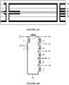
- FIGURE 2AAn example implementation of a preferred embodiment is shown in FIGURE 2A (cross-sectional view).
- the LC resonator 110is constructed on a laminate substrate, having a number of isolative layers (1, 3-7, 9) and conductive layers (2, 8).
- the LC resonator 110is formed from a parallel plate capacitor 11, of which a first plate is coupled to a ground plane 14 by a conductive via 10, and a strip inductor 12, which is coupled to the second plate of the capacitor 11 by a conductive via 10 and is coupled to the ground plane 14 by another conductive via 10.
- the ground planemay extend over all or most of the surface of the substrate on one side, and thus extend over a greater area than the strip inductor; alternatively, the ground plane may be a second strip inductor on the opposing side of the substrate that is of substantially the same size and extent, or may alternatively extend over any other suitable area.
- the resonator 110may be coupled to at coupling point 13. If constructed on a laminate substrate, the LC resonator 110 may include any number of layers made of any material.
- the resonator 110may include epoxy prepreg layers 4 and 6; FR-4 core layers 3, 7; copper conductive layers 2, 8; and hafnium oxide high-k dielectric layer 5, with copper vias 10.
- the layers, vias, and elementsmay be of any shape, size, thickness, etc.
- the dielectric material separating the plates of the capacitorin this case layer 5 may be a standard isolative layer (e.g., a core layer), but may alternatively be a different dielectric material (e.g., a dielectric material with higher k or otherwise suitable to serve as an insulator for the capacitor 11).
- FIGURE 2Bcross-sectional view
- FIGURE 3top-down view
- the LC resonator 110is constructed on a semiconductor chip substrate 15.
- the LC resonator 110is formed from a parallel plate capacitor 18 and a strip inductor 20, both coupled to a ground contact 21 by through-substrate vias 16.
- the resonator 110may be coupled to at coupling point 19. If constructed on a semiconductor or insulator chip substrate, the resonator 110 may include any materials fabricated in any manner.
- the resonator 110may include a silicon dioxide substrate 15, a silicon dioxide or silicon nitride capacitor dielectric pad 17, with metallic pads/traces/vias fabricated using electroplated copper or aluminum (16, 18-21; note: seed layer not pictured).
- the capacitor dielectricmay be a similar material to the substrate or may be a different material (for fabrication reasons, dielectric constant, etc.).
- the LC resonatoris constructed on a semiconductor chip substrate, and the LC resonator 110 is formed from a buried parallel plate capacitor and a strip inductor.
- the strip inductormay be covered by an isolative layer and/or a shielding layer, which may prevent electromagnetic coupling between the strip inductor and neighboring packaged elements (e.g., strip inductors, traces, etc.). Additionally or alternatively, the resonator may be physically distanced from other packaged elements to avoid mutual electromagnetic coupling (in such example implementations and variations where mutual electromagnetic coupling is not desired).
- LC resonators 110may include multiple tapping points to enable modification of the impedance of the LC resonator 110 (as seen by coupled or matching circuits). Tapping points may also be referred to as coupling points, and may perform the same function; alternatively, they may perform different functions. Additionally or alternatively, tapping of the resonator may be used to modify impedance, time delay, resonance frequency, etc.
- the inductor of the LC resonator 110may include multiple tapping points 22-28.
- An equivalent circuit of this exampleis as shown in FIGURE 4B .
- a tapping point of an inductor or inductive elementmay include conductive layers of the substrate that extend to a point along a portion of the inductor that passes through the substrate (e.g., to a point along a via that comprises a portion of the resonator).
- the inductance of the total inductor(as seen by a coupling element or experienced by a signal passing through the resonator) is variable depending on the point along the conductive path at which a signal is sampled from, or, similarly, the point at which a tap is physically and electrically coupled to the conductive path.
- the inductance, and thus the frequency response and/or time delay,may be varied by sampling the signal (or coupling to the resonator) at various tapping points.
- the capacitor of the LC resonator 110may include multiple tapping points 29-31.
- An equivalent circuit of this exampleis as shown in FIGURE 5B .
- the capacitorincludes two conductive planar regions that are subdivided into electrically isolated subregions, as shown in FIGURE 5A . Each of these subregions is coupled to a tapping point, and the division of the capacitive element into multiple capacitive subelements in this manner can enable variation of the capacitance of the LC resonator as seen by coupled elements or signals passing through the LC resonator (by variation of the tapping point at which elements are coupled to the multi-tapped LC resonator). Selection of the variable capacitance is preferably performed in a similar manner as for a multi-tapped inductor as described above, but can additionally or alternatively be performed in any suitable manner.
- An LC resonator 110may include multiple tapping points on both the capacitive element and the inductive element.
- a component of an LC resonator 110may be coupled to in any manner.
- a switche.g., a transistor
- a switchmay be coupled between tapping points, allowing those tapping points to be shorted (e.g., a switch between tapping points 30 and 31 could enable selective shorting of C2).
- a component of an LC resonator 110includes multiple tapping points and a coupling point at which it is coupled to other LC resonators (e.g., resistively coupled, capacitively coupled, inductively coupled, electromagnetically coupled), they may be selectively coupled in any suitable manner.
- a set of switchese.g., transistors, a multi-input / single-output multiplexer, etc.
- LC resonators 110may integrate or be coupled to tunable circuit elements (e.g., capacitors, inductors, transistors, resistors) to change their tuning properties.
- tunable circuit elementse.g., capacitors, inductors, transistors, resistors
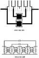
- FIGURES 6A and 6BSome examples of tunable LC resonators 110 are as shown in FIGURES 6A and 6B .
- the LC resonator 110may include one or more varactors in parallel with the LC resonator 110, enabling a tunable capacitance of the resonator.
- the LC resonator 110may include a single or multitude of capacitor-transistor series combinations, which allow tuning of the capacitance of the LC resonator 110 via different permutations of transistors being switched on or off.
- the capacitor in the capacitor-transistor series combinationmay be replaced with a varactor to reduce the number of switches needed or increase the resolution of the tuning.
- Tuning of the LC resonatorsmay also be done permanently at the end of the manufacturing process by adding (e.g. by way of 3D metal printing) or removing (e.g. milling) material from traces, inductor or the plate of any capacitor in the circuit.
- capacitors and/or inductorsmay be tuned by blowing small fuses implemented as traces in the substrate.
- LC resonators 110 of the delay filter 100are preferably coupled in parallel to form the delay filter 100 (or part of the delay filter 100). While LC resonators 110 may be coupled in any manner (e.g., resistively), LC resonators 110 are preferably coupled to each other capacitively (using capacitive intra-filter coupling elements 120) and/or inductively (by positioning inductors of LC resonators 110 to enable magnetic coupling between the inductors) or in any combination of the 3 coupling methods (e.g. 50% capacitive and 50% inductive).
- Intra-filter elements 120function to couple LC resonators 110 of the delay filter 100. Similarly to components of the LC resonator 110, intra-filter elements are preferably passive capacitive, resistive, and/or inductive elements, but intra-filter elements may be any active or passive components capable of coupling LC resonators no. Intra-filter elements 120 are preferably constructed from a combination of metallization layer strips, vias, and the substrate, but may additionally or alternatively be constructed in any manner. For example, a capacitive intra-filter element 120 may be a packaged capacitor surface-mounted to a substrate containing the LC resonators 110. As another example, a capacitive intra-filter element 120 may be constructed in a substantially similar manner to a capacitor of an LC resonator 110.
- an example delay filter 110includes LC resonators 110 coupled both capacitively and inductively.
- An equivalent circuit modelis as shown in FIGURE 7B .
- the coupling capacitorsare mounted to the surface of the substrate whereas the buried capacitors associated with each LC resonator are embedded within the substrate.
- the coupling capacitorsmay be similarly embedded, or may be otherwise suitably configured.
- the microstrip inductors of a subset of the resonatorsinclude two distinct conductive regions that extend across a surface of the substrate, and are separated laterally on the surface.
- Inductive coupling(e.g., by way of mutual inductance) between resonators is accomplished in this example by one of the laterally-separated portions of the inductor of one resonator coupling with one of the portions of the inductor of another resonator.
- the bilateral configuration of this exampleprovides for inductive coupling with a resonator positioned at either lateral position neighboring the resonator.
- a second example delay filter 110also includes LC resonators 110 coupled both capacitively and inductively.
- An equivalent circuit modelis as shown in FIGURE 8B .
- Inductive couplingis preferably accomplished by placing microstrip inductors in proximity to each other, but may additionally or alternatively be accomplished in any manner.
- inductors of separate LC resonators 110may be braided or otherwise positioned to accomplish inductive coupling between the LC resonators 110.
- inductive couplingmay include electromagnetic coupling between inductors that are not in direct electric contact (e.g., the changing magnetic flux generated by current flowing through one inductor or inductive element may induce a current in another inductor or inductive element); it may additionally or alternatively include direct electrical coupling of an inductor between two inductors, that are thereby inductively coupled.
- Input matching elements 130function to couple LC resonators 110 to an input and/or output of the delay filter 100 with the desired impedance.
- Input matching elements 130preferably include circuits comprising passive capacitive, resistive, and/or inductive elements, but input matching elements 130 may be any active or passive combination of components (including trace or microstrip components) capable of coupling the delay filter 100 to an external circuit.
- Input matching elements 130are preferably constructed from a combination of metallization layer strips, vias, and the substrate, but may additionally or alternatively be constructed in any manner.
- an input coupling element 130may comprise a circuit of packaged capacitors and inductors surface-mounted to a substrate containing the LC resonators 110.
- components of an input coupling element 130may be constructed in a substantially similar manner to those of an LC resonator 110. Similar to LC resonators 110, input matching elements 130 may incorporate tapped or otherwise tunable capacitive and/or inductive elements. In another embodiments the input coupling element may incorporate tunable resistors.
- example filters 100may be coupled to using a tapped capacitor LC resonator-based coupler 1301, a tapped inductor LC resonator-based coupler 1302, an inductively-coupled LC resonator-based coupler 1303, and/or a transmission line coupler 1304.
- input matching elements 130may be independent of LC resonators 110, additionally or alternatively, input matching elements 130 may be merged (partially or fully) with resonators 110 of the filter 100.
- the LC resonator 110may include an additional capacitive and/or inductive element, in parallel or in series with the primary capacitive and inductive elements, that may function as an input matching element 130.
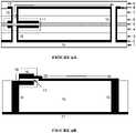
- inductors and capacitors of LC resonators 110 of the delay filter 100are separated onto separate chips, dies, and/or substrates and are coupled by wire-bonding, traces on an underlying substrate, flip-chip bonding, or some other technique. Some examples of this separation as shown in FIGURE 10A .
- the delay filter 100includes switches (e.g., to switch between taps of tapped inductors/capacitors), the switches may be isolated from resonators and coupled by wire-bonding, traces on an underlying substrate, flip-chip bonding, or some other technique, as shown in FIGURE 10B .
- the delay filter 100may comprise any number of switches, and switches (or a set of switches) may be any suitable components capable of selectively coupling the taps and/or coupling points of resonators 110 or other components to circuit common rails, grounds, and/or circuit inputs/outputs.
- switchesmay include mechanical switches, mechanical relays, solid-state relays, transistors, silicon controlled rectifiers, triacs, and/or digital switches.
- Switches of the set of switchesmay be operable electronically by a tuning circuit or other suitable controller, but may additionally or alternatively be set in any manner. For example, switches may be manually set by a circuit user.
- switchesmay be one-time-use junctions that are configured into a desired configuration when the delay filter 100 is manufactured (e.g., by soldering, annealing, fusing, or any other suitable manner of irreversible configuration), resulting in a desired overall delay filter 100 configuration (e.g., group delay value).
- Switchesare preferably operable between one or more switch states, in which a state of the switch corresponds to coupling between two or more system components.
- a switche.g., transistor
- a switchmay be operable in a first switch state that couples a first tapping point to a coupling point of a resonator, and in a second switch state that couples a second tapping point to a coupling point of a resonator.
- a switchmay be operable in a first switch state that couples one of a set of resonators to a common rail (e.g., a ground plane) of the system, in order to place it in the signal path of a signal passing through the time delay filter; this switch may be operable in a second switch state that decouples the resonator from the common rail, thereby removing the resonator from the signal path (and reducing the overall time delay applied by the time delay filter).
- a common raile.g., a ground plane
- separate chips/diesmay be laterally separated on a substrate, but additionally or alternatively, they may be stacked vertically (or in any other manner). Coupling between circuit elements may be between elements on either the same or separate chips. For example, inductors on a first printed circuit board may be magnetically coupled to inductors on a second printed circuit board in cases in which the two PCBs are positioned so as to bring the inductors (between which magnetic coupling is desired) into close proximity. Additionally or alternatively, other three-dimensional configurations of circuit elements may be leveraged to achieve electromagnetic coupling in any suitable manner.
- the time delay filterincludes a substrate and an LC resonator.
- the substrateis a laminated circuit board that is comprised of several layers and has two broad, substantially parallel outer surfaces (e.g., a top and bottom surface, though the substrate may be in any suitable orientation).
- the resonatorincludes a capacitive element and an inductive element, coupled together into an LC circuit that is connected in parallel between a conductive contact point (e.g., a coupling point) on the first surface and a ground plane (e.g., a conductive region) on the second surface.
- the inductive elementis a strip inductor that is formed by a conductive region (e.g., a metallized strip) on the first surface, and connected to the capacitive element and the ground plane by a pair of conductive vias.
- the first viais a through-hole via passing through the substrate (e.g., through several isolative and/or conductive layers of the substrate) to the ground plane
- the second viais a partial via that passes through the substrate to an intermediate position within the substrate where the capacitive element is located.
- the capacitive elementwhich may be a parallel plate capacitor or any other suitable capacitive element, completes the LC circuit while interrupting the continuous conductive region (e.g., byway of a dielectric barrier between two sides, such as parallel plates, of the capacitive element).
- the strip inductor, the first, second, and third vias, the capacitor, and the ground planeform a loop.
- This loopencloses an area that defines a normal axis, and the normal axis is substantially parallel to the plane(s) of the surfaces of the substrate; in other words, the conductive loop passes through the substrate in two locations (in this example, the locations of the vias) and lies adjacent to the substrate on two contralateral sides of the substrate.
- the LC resonators 110may have a certain inductance and capacitance per unit length that repeats in a harmonic fashion over the length of the resonator, and the time delay filter 100 may therefore be well-represented using a distributed inductor and capacitor model (e.g., a transmission line model).
- the LC resonators 110may be formed from localized discrete components (e.g., ceramic capacitors, wound-wire inductors) such that the time delay filter 100 is well-represented using a lumped-element model.
- a subset of LC resonatorsmay be represented by a distributed model and another subset of LC resonators may be represented by a lumped element model.
- resonatorsmay be coupled in a large horseshoe pattern (similar to the magnetic coupling of FIGURES 7A and 8A ).
- resonatorsmay be coupled in a meander pattern or a zigzag pattern (respectively).
- Resonators 110may be positioned and coupled in any manner.
Landscapes
- Engineering & Computer Science (AREA)
- Power Engineering (AREA)
- Filters And Equalizers (AREA)
- Fixed Capacitors And Capacitor Manufacturing Machines (AREA)
- Control Of Motors That Do Not Use Commutators (AREA)
- Coils Or Transformers For Communication (AREA)
Description
- This invention relates to time delay filters.
- Time delay elements are used in a variety of analog circuits to cause analog signals to experience a time delay. In particular, time delay elements are particularly important for RF transceivers, where they may be used for amplifier pre-distortion, feed-forward linearization, and active interference cancellation techniques. Of course, such time delay elements may find use in a wide variety of applications involving analog signal transmission, processing, and/or synthesis.
- Unfortunately, traditional delay elements (e.g., ceramic filters, SAW filters, coaxial cables, waveguide cavity resonator-based filters) may limit the performance of analog circuits; in particular, RF transceivers, due to one or more of the following problems: excessive size, excessive cost, excessive complexity, poor manufacturability, lack of adjustability, high loss, high amplitude ripple, or high phase ripple.
US2014292443 discloses a single loop resonant circuit constituting a building block for more complex filters which may be used in a time delay element. - Thus, there is a need in the field of analog circuits to create new and useful time delay filters. This invention provides such new and useful time delay filters.
FIGURE 1A and 1B is a schematic representation of a delay filter of a preferred embodiment;FIGURE 2A is a cross-sectional example representation of a resonator of a delay filter of a preferred embodiment;FIGURE 2B is a cross-sectional example representation of a resonator of a delay filter of a preferred embodiment;FIGURE 3 is a top-down example representation of a resonator of a delay filter of a preferred embodiment;FIGURE 4A is a cross-sectional example representation of a resonator of a delay filter of a preferred embodiment;FIGURE 4B is a circuit representation of a resonator of a delay filter of a preferred embodiment;FIGURE 5A is a cross-sectional example representation of a resonator of a delay filter of a preferred embodiment;FIGURE 5B is a circuit representation of a resonator of a delay filter of a preferred embodiment;FIGURE 6A is a circuit representation of a tunable resonator of a delay filter of a preferred embodiment;FIGURE 6B is a circuit representation of a tunable resonator of a delay filter of a preferred embodiment;FIGURE 7A is a top-down example representation of a delay filter of a preferred embodiment;FIGURE 7B is a circuit representation of a delay filter of a preferred embodiment;FIGURE 8A is a top-down example representation of a delay filter of a preferred embodiment;FIGURE 8B is a circuit representation of a delay filter of a preferred embodiment;FIGURE 9 is a circuit representation of input and output matching elements of a delay filter of a preferred embodiment;FIGURE 10A is a side view representation of a delay filter of a variation of a preferred embodiment;FIGURE 10B is a side view representation of a delay filter of a variation of a preferred embodiment; andFIGUREs 11A-C are circuit representations of LC resonator arrangements of a delay filter of a preferred embodiment.- The following description of the preferred embodiments of the invention is not intended to limit the invention to these preferred embodiments, but rather to enable any person skilled in the art to make and use this invention.
- The systems described herein may increase performance of full-duplex transceivers (and other applicable systems) by enabling high accuracy time delay filtering without prohibitive increases in circuit complexity and/or cost. Other applicable systems include active sensing systems (e.g., RADAR), wired communications systems, wireless communications systems, channel emulators, reflectometers, PIM analyzers and/or any other suitable system, including communication systems where transmit and receive bands are close in frequency, but not overlapping.
- As shown in
FIGURE 1A , atime delay filter 100 includes one ormore LC resonators 110. Thetime delay filter 100 may additionally includeintra-filter coupling elements 120 and/orinput matching elements 130. Thetime delay filter 100 may additionally or alternatively include any number of LC resonators 110 (e.g., the set ofLC resonators 110 may contain only a single LC resonator). Thetime delay filter 100 may additionally or alternatively include any suitable components coupled to the LC resonator(s) 110 that aid or otherwise contribute the production of a time delay, such as passive or active components (e.g., capacitors, transistors, switches, etc.), integrated components (e.g., conductive layers and/or traces), or any other suitable components. - The
time delay filter 100 preferably functions to produce a substantially frequency-invariant group delay for analog signals within a particular frequency band of interest; typically a frequency band within the range of radio frequencies (RF), but alternatively any suitable frequency band in any suitable frequency range. A group delay of an analog signal will delay the amplitude envelope of each frequency component of the signal; a frequency-invariant group delay will apply an equal time delay to the amplitude envelope of each frequency component of the signal. - The
time delay filter 100 can additionally or alternatively function to increase the performance of signal transceivers (or other applicable systems; e.g., phased antenna arrays) by enabling high accuracy, adjustable, and/or reconfigurable group delay of signals without prohibitive increases in circuit complexity and/or cost. - The
time delay filter 100 preferably has a relatively low and frequency-invariant (in a frequency band of interest) insertion loss (e.g., 1 dB, 3 dB, or 5 dB of insertion loss and/or attenuation). In other words, the magnitude of the frequency response of thetime delay filter 100 is substantially flat over the range of frequencies of interest (e.g., over the range of radio frequencies) and has a magnitude ripple that is small relative to the signal magnitude (e.g., 10×, 100×, or 1000× smaller). Alternatively, thetime delay filter 100 may have any suitable insertion loss, that varies with frequency in any suitable manner. - The
time delay filter 100 preferably is constructed from lumped and/or distributed inductors and capacitors that are integrated into the substrate of a laminate (e.g., a printed circuit board), of a microchip (e.g., a silicon substrate), or any other suitable circuit substrate. Integration of thetime delay filter 100 may substantially reduce cost and size of thetime delay filter 100. - Portions of the time delay filter may additionally or alternatively be added to the substrate as discrete components. For example, the LC resonator(s) 110 of the
time delay filter 100 may be integrated into the substrate, and input matching element(s) 130 and/or intra-filter coupling element(s) 120 may be coupled to the substrate and/or the LC resonators as discrete components (e.g., via wire bonding, surface mounting, etc.). - The
time delay filter 100 is preferably implemented using analog circuitry, but additionally or alternatively may be implemented by digital circuitry or any combination of analog and digital circuitry. Analog circuitry is preferably implemented using a combination of the circuit substrate and metallized/conductive layers as described above, but can additionally or alternatively be implemented using analog integrated circuits (ICs) and/or discrete components (e.g., capacitors, inductors, resistors, transistors), wires, transmission lines, transformers, couplers, hybrids, waveguides, digital components, mixed-signal components, or any other suitable components. Digital circuitry is preferably implemented using a general-purpose processor, a digital signal processor, an application specific integrated circuit (ASIC), a field programmable gate array (FPGA) and/or any suitable processor(s) or circuit(s). Thetime delay filter 100 is preferably preconfigured structurally to provide a given time delay or set of time delays, but may additionally or alternatively include memory to store configuration data, or be configured using externally stored configuration data or in any suitable manner. - The
time delay filter 100 may include multiple coupling points 113 (i.e., points at which other circuits may couple to the time delay filter 100) to enable either or both of variable impedance of the time delay filter and variable delay of the time delay filter (as discussed in subsequent sections). - The
time delay filter 100 may also alter impedance or delay of thetime delay filter 100 through use of tunable elements in theLC resonators 110 or matchingelements 130; i.e., as opposed to modifying impedance by coupling at a different coupling point, impedance may be modified using variable capacitors and/or inductors. - Each
LC resonator 110 of thedelay 100 functions to contribute a time delay to an input signal of thetime delay filter 100. As shown inFIGURE 1A ,LC resonators 110 are preferably coupled in parallel; alternatively,LC resonators 110 may be coupled in any manner.LC resonators 110 preferably include one ormore coupling points 113, as shown inFIGURE 1B , at which other components of the time delay filter (e.g.,additional resonators 110, matchingelements 130, coupling elements, etc.) are coupled (e.g., electrically connected) to the resonator. Coupling may be resistive (e.g., by a wire, metallized layer, or any other suitable conductive material), capacitive (e.g., by a discrete capacitor, mutual capacitance, etc.), inductive (e.g., by a discrete inductor, mutual inductance, etc.), electromagnetic (e.g., radiative coupling), or any other suitable manner. Additionally or alternatively, LC resonators may be coupled to in any suitable manner. - The
LC resonator 110 is preferably optimized to reduce the number of components required in time delay filter construction (and therefore complexity/cost of any applicable system using a time delay filter) as well as to provide low insertion loss. - Each
LC resonator 110 preferably has substantially the same frequency response and produces a substantially similar time delay. Accordingly, the delay of the time delay filter is preferably approximately equal to the number ofLC resonators 110 multiplied by the average time delay of theLC resonators 110. In such an implementation, the total delay experienced by a signal passing through the time delay filter may be adjustable by selecting the number ofLC resonators 110 switched into the signal path. Alternatively, the time delay filter may have a number of LC resonators with different frequency responses that may produce different time delays, and in such cases the delay of the time delay filter is preferably approximately equal to the sum of the time delay of eachLC resonator 110 in the signal path. Alternatively, eachLC resonator 110 may have any impedance and/or any time delay, and thetime delay filter 100 may have any input/output impedance and total time delay, adjustable in any suitable manner. - Each
LC resonator 110 preferably includes a substantially capacitive element 111 (i.e., an element whose reactance, in a frequency band of interest, is negative) and a substantially inductive element 112 (i.e., an element whose reactance, in a frequency band of interest, is positive) placed in parallel. Alternatively, eachLC resonator 110 may include any circuit elements such that the impedance of theresonator 110 is approximately characterized by:


- The
LC resonator 110 is preferably constructed in a laminate or chip substrate from a combination of metallization layer strips (e.g., strip inductor, microstrip, etc.), vias (e.g., through-hole vias, partial vias, buried vias, metallized slots, etc.), and the substrate itself. Additionally, theLC resonator 110 may include high-k dielectric layers. Alternatively, theLC resonator 110 may be constructed using any suitable materials. - As shown in
FIGUREs 2A, 2B , and3 theLC resonator 110 is preferably constructed from a combination of a parallel plate capacitor and a strip inductor on a laminate substrate or a semiconductor/insulator chip substrate. Such a parallel plate capacitor preferably includes a first conductive planar region separated from a second conductive planar region by a dielectric material, and the first and second conductive planar regions are preferably substantially parallel (e.g., as uniformly parallel as manufacturing tolerances may permit); however, a parallel plate capacitor may additionally or alternatively include any suitable subcomponents configured in any suitable manner. Alternatively, theLC resonator 110 may be constructed from any other suitable capacitive/inductive elements (e.g., a spiral inductor or interdigitated finger capacitor). For example, anLC resonator 110 may include a braided inductive element (i.e., an inductive element comprising several inductive subelements in parallel, separated by an insulator, 'braided' or otherwise positioned near each other). Such a braided inductive element is preferably formed from layers of the substrate including regions of alternately isolative and conductive material, which, when stacked together to form the substrate, are configured into a three-dimensional braided structure. Alternatively, a braided inductive element may be formed from any suitable materials, in any suitable manner. - An example implementation of a preferred embodiment is shown in
FIGURE 2A (cross-sectional view). In this implementation, theLC resonator 110 is constructed on a laminate substrate, having a number of isolative layers (1, 3-7, 9) and conductive layers (2, 8). TheLC resonator 110 is formed from a parallel plate capacitor 11, of which a first plate is coupled to aground plane 14 by a conductive via 10, and astrip inductor 12, which is coupled to the second plate of the capacitor 11 by a conductive via 10 and is coupled to theground plane 14 by another conductive via 10. The ground plane may extend over all or most of the surface of the substrate on one side, and thus extend over a greater area than the strip inductor; alternatively, the ground plane may be a second strip inductor on the opposing side of the substrate that is of substantially the same size and extent, or may alternatively extend over any other suitable area. Theresonator 110 may be coupled to atcoupling point 13. If constructed on a laminate substrate, theLC resonator 110 may include any number of layers made of any material. For example, in this example implementation, theresonator 110 may includeepoxy prepreg layers core layers conductive layers 2, 8; and hafnium oxide high-k dielectric layer 5, withcopper vias 10. The layers, vias, and elements may be of any shape, size, thickness, etc. Note that in particular the dielectric material separating the plates of the capacitor (in this case layer 5) may be a standard isolative layer (e.g., a core layer), but may alternatively be a different dielectric material (e.g., a dielectric material with higher k or otherwise suitable to serve as an insulator for the capacitor 11). - A second example implementation of a preferred embodiment is as shown in
FIGURE 2B (cross-sectional view) andFIGURE 3 (top-down view). In this implementation, theLC resonator 110 is constructed on asemiconductor chip substrate 15. TheLC resonator 110 is formed from aparallel plate capacitor 18 and astrip inductor 20, both coupled to aground contact 21 by through-substrate vias 16. Theresonator 110 may be coupled to atcoupling point 19. If constructed on a semiconductor or insulator chip substrate, theresonator 110 may include any materials fabricated in any manner. For example, in this example implementation, theresonator 110 may include asilicon dioxide substrate 15, a silicon dioxide or silicon nitridecapacitor dielectric pad 17, with metallic pads/traces/vias fabricated using electroplated copper or aluminum (16, 18-21; note: seed layer not pictured). Similar to the first example implementation, the capacitor dielectric may be a similar material to the substrate or may be a different material (for fabrication reasons, dielectric constant, etc.). - In a third example implementation of a preferred embodiment related to the second example implementation, the LC resonator is constructed on a semiconductor chip substrate, and the
LC resonator 110 is formed from a buried parallel plate capacitor and a strip inductor. The strip inductor may be covered by an isolative layer and/or a shielding layer, which may prevent electromagnetic coupling between the strip inductor and neighboring packaged elements (e.g., strip inductors, traces, etc.). Additionally or alternatively, the resonator may be physically distanced from other packaged elements to avoid mutual electromagnetic coupling (in such example implementations and variations where mutual electromagnetic coupling is not desired). LC resonators 110 may include multiple tapping points to enable modification of the impedance of the LC resonator 110 (as seen by coupled or matching circuits). Tapping points may also be referred to as coupling points, and may perform the same function; alternatively, they may perform different functions. Additionally or alternatively, tapping of the resonator may be used to modify impedance, time delay, resonance frequency, etc.- For example, as shown in
FIGURE 4A , the inductor of theLC resonator 110 may include multiple tapping points 22-28. An equivalent circuit of this example is as shown inFIGURE 4B . A tapping point of an inductor or inductive element may include conductive layers of the substrate that extend to a point along a portion of the inductor that passes through the substrate (e.g., to a point along a via that comprises a portion of the resonator). In this example, the inductance of the total inductor (as seen by a coupling element or experienced by a signal passing through the resonator) is variable depending on the point along the conductive path at which a signal is sampled from, or, similarly, the point at which a tap is physically and electrically coupled to the conductive path. The inductance, and thus the frequency response and/or time delay, may be varied by sampling the signal (or coupling to the resonator) at various tapping points. - As another example, as shown in
FIGURE 5A , the capacitor of theLC resonator 110 may include multiple tapping points 29-31. An equivalent circuit of this example is as shown inFIGURE 5B . In example implementation, the capacitor includes two conductive planar regions that are subdivided into electrically isolated subregions, as shown inFIGURE 5A . Each of these subregions is coupled to a tapping point, and the division of the capacitive element into multiple capacitive subelements in this manner can enable variation of the capacitance of the LC resonator as seen by coupled elements or signals passing through the LC resonator (by variation of the tapping point at which elements are coupled to the multi-tapped LC resonator). Selection of the variable capacitance is preferably performed in a similar manner as for a multi-tapped inductor as described above, but can additionally or alternatively be performed in any suitable manner. - Multiple tapping points allow for either varying the impedance of the resonator and/or generating a differential signal from a single ended input signal (e.g. when using both tapping points around C2 in
FIGURE 5B ). AnLC resonator 110 may include multiple tapping points on both the capacitive element and the inductive element. - If a component of an
LC resonator 110 includes multiple tapping points, they may be coupled to in any manner. For example, a switch (e.g., a transistor) may be coupled between aresonator 110 input and multiple tapping points, enabling a selection of tapping points. As another example, a switch may be coupled between tapping points, allowing those tapping points to be shorted (e.g., a switch between tappingpoints - If a component of an
LC resonator 110 includes multiple tapping points and a coupling point at which it is coupled to other LC resonators (e.g., resistively coupled, capacitively coupled, inductively coupled, electromagnetically coupled), they may be selectively coupled in any suitable manner. For example, a set of switches (e.g., transistors, a multi-input / single-output multiplexer, etc.) may be coupled between the tapping points (taps) and the coupling point, enabling selection and/or adjustment of the impedance of the resonator as seen by components (e.g.,resonators 110, matching elements 130) coupled to the coupling point. - In addition to having tapping points,
LC resonators 110 may integrate or be coupled to tunable circuit elements (e.g., capacitors, inductors, transistors, resistors) to change their tuning properties. Some examples oftunable LC resonators 110 are as shown inFIGURES 6A and 6B . As shown inFIGURE 6A , theLC resonator 110 may include one or more varactors in parallel with theLC resonator 110, enabling a tunable capacitance of the resonator. As shown inFIGURE 6B , theLC resonator 110 may include a single or multitude of capacitor-transistor series combinations, which allow tuning of the capacitance of theLC resonator 110 via different permutations of transistors being switched on or off. In another embodiment the capacitor in the capacitor-transistor series combination may be replaced with a varactor to reduce the number of switches needed or increase the resolution of the tuning. - Tuning of the LC resonators (and hence the delay filter) may also be done permanently at the end of the manufacturing process by adding (e.g. by way of 3D metal printing) or removing (e.g. milling) material from traces, inductor or the plate of any capacitor in the circuit. Alternatively capacitors and/or inductors may be tuned by blowing small fuses implemented as traces in the substrate.
- As previously described,
LC resonators 110 of thedelay filter 100 are preferably coupled in parallel to form the delay filter 100 (or part of the delay filter 100). WhileLC resonators 110 may be coupled in any manner (e.g., resistively),LC resonators 110 are preferably coupled to each other capacitively (using capacitive intra-filter coupling elements 120) and/or inductively (by positioning inductors ofLC resonators 110 to enable magnetic coupling between the inductors) or in any combination of the 3 coupling methods (e.g. 50% capacitive and 50% inductive). Intra-filter elements 120 function to coupleLC resonators 110 of thedelay filter 100. Similarly to components of theLC resonator 110, intra-filter elements are preferably passive capacitive, resistive, and/or inductive elements, but intra-filter elements may be any active or passive components capable of coupling LC resonators no.Intra-filter elements 120 are preferably constructed from a combination of metallization layer strips, vias, and the substrate, but may additionally or alternatively be constructed in any manner. For example, a capacitiveintra-filter element 120 may be a packaged capacitor surface-mounted to a substrate containing theLC resonators 110. As another example, a capacitiveintra-filter element 120 may be constructed in a substantially similar manner to a capacitor of anLC resonator 110.- As shown in a top-down view in
FIGURE 7A , anexample delay filter 110 includesLC resonators 110 coupled both capacitively and inductively. An equivalent circuit model is as shown inFIGURE 7B . In this example, the coupling capacitors are mounted to the surface of the substrate whereas the buried capacitors associated with each LC resonator are embedded within the substrate. Alternatively, the coupling capacitors may be similarly embedded, or may be otherwise suitably configured. In this example, the microstrip inductors of a subset of the resonators include two distinct conductive regions that extend across a surface of the substrate, and are separated laterally on the surface. Inductive coupling (e.g., by way of mutual inductance) between resonators is accomplished in this example by one of the laterally-separated portions of the inductor of one resonator coupling with one of the portions of the inductor of another resonator. The bilateral configuration of this example provides for inductive coupling with a resonator positioned at either lateral position neighboring the resonator. - As shown in a top-down view in
FIGURE 8A , a secondexample delay filter 110 also includesLC resonators 110 coupled both capacitively and inductively. An equivalent circuit model is as shown inFIGURE 8B . - Inductive coupling is preferably accomplished by placing microstrip inductors in proximity to each other, but may additionally or alternatively be accomplished in any manner. For example, inductors of
separate LC resonators 110 may be braided or otherwise positioned to accomplish inductive coupling between theLC resonators 110. Note that inductive coupling may include electromagnetic coupling between inductors that are not in direct electric contact (e.g., the changing magnetic flux generated by current flowing through one inductor or inductive element may induce a current in another inductor or inductive element); it may additionally or alternatively include direct electrical coupling of an inductor between two inductors, that are thereby inductively coupled. Input matching elements 130 function to coupleLC resonators 110 to an input and/or output of thedelay filter 100 with the desired impedance.Input matching elements 130 preferably include circuits comprising passive capacitive, resistive, and/or inductive elements, butinput matching elements 130 may be any active or passive combination of components (including trace or microstrip components) capable of coupling thedelay filter 100 to an external circuit.Input matching elements 130 are preferably constructed from a combination of metallization layer strips, vias, and the substrate, but may additionally or alternatively be constructed in any manner. For example, aninput coupling element 130 may comprise a circuit of packaged capacitors and inductors surface-mounted to a substrate containing theLC resonators 110. As another example, components of aninput coupling element 130 may be constructed in a substantially similar manner to those of anLC resonator 110. Similar toLC resonators 110,input matching elements 130 may incorporate tapped or otherwise tunable capacitive and/or inductive elements. In another embodiments the input coupling element may incorporate tunable resistors.- Some examples of
input matching elements 130 are as shown inFIGURE 9 . As shown inFIGURE 9 , example filters 100 may be coupled to using a tapped capacitor LC resonator-basedcoupler 1301, a tapped inductor LC resonator-basedcoupler 1302, an inductively-coupled LC resonator-basedcoupler 1303, and/or a transmission line coupler 1304. - While
input matching elements 130 may be independent ofLC resonators 110, additionally or alternatively,input matching elements 130 may be merged (partially or fully) withresonators 110 of thefilter 100. For example, theLC resonator 110 may include an additional capacitive and/or inductive element, in parallel or in series with the primary capacitive and inductive elements, that may function as aninput matching element 130. - In a variation of a preferred embodiment, inductors and capacitors of
LC resonators 110 of thedelay filter 100 are separated onto separate chips, dies, and/or substrates and are coupled by wire-bonding, traces on an underlying substrate, flip-chip bonding, or some other technique. Some examples of this separation as shown inFIGURE 10A . - Likewise, if the
delay filter 100 includes switches (e.g., to switch between taps of tapped inductors/capacitors), the switches may be isolated from resonators and coupled by wire-bonding, traces on an underlying substrate, flip-chip bonding, or some other technique, as shown inFIGURE 10B . - The
delay filter 100 may comprise any number of switches, and switches (or a set of switches) may be any suitable components capable of selectively coupling the taps and/or coupling points ofresonators 110 or other components to circuit common rails, grounds, and/or circuit inputs/outputs. For example, switches may include mechanical switches, mechanical relays, solid-state relays, transistors, silicon controlled rectifiers, triacs, and/or digital switches. Switches of the set of switches may be operable electronically by a tuning circuit or other suitable controller, but may additionally or alternatively be set in any manner. For example, switches may be manually set by a circuit user. As another example, switches may be one-time-use junctions that are configured into a desired configuration when thedelay filter 100 is manufactured (e.g., by soldering, annealing, fusing, or any other suitable manner of irreversible configuration), resulting in a desiredoverall delay filter 100 configuration (e.g., group delay value). - Switches are preferably operable between one or more switch states, in which a state of the switch corresponds to coupling between two or more system components. For example, a switch (e.g., transistor) may be operable in a first switch state that couples a first tapping point to a coupling point of a resonator, and in a second switch state that couples a second tapping point to a coupling point of a resonator. In another example, a switch may be operable in a first switch state that couples one of a set of resonators to a common rail (e.g., a ground plane) of the system, in order to place it in the signal path of a signal passing through the time delay filter; this switch may be operable in a second switch state that decouples the resonator from the common rail, thereby removing the resonator from the signal path (and reducing the overall time delay applied by the time delay filter).
- As shown in
FIGUREs 10A and 10B , separate chips/dies may be laterally separated on a substrate, but additionally or alternatively, they may be stacked vertically (or in any other manner). Coupling between circuit elements may be between elements on either the same or separate chips. For example, inductors on a first printed circuit board may be magnetically coupled to inductors on a second printed circuit board in cases in which the two PCBs are positioned so as to bring the inductors (between which magnetic coupling is desired) into close proximity. Additionally or alternatively, other three-dimensional configurations of circuit elements may be leveraged to achieve electromagnetic coupling in any suitable manner. - In an example implementation of a preferred embodiment, the time delay filter includes a substrate and an LC resonator. The substrate is a laminated circuit board that is comprised of several layers and has two broad, substantially parallel outer surfaces (e.g., a top and bottom surface, though the substrate may be in any suitable orientation). The resonator includes a capacitive element and an inductive element, coupled together into an LC circuit that is connected in parallel between a conductive contact point (e.g., a coupling point) on the first surface and a ground plane (e.g., a conductive region) on the second surface. The inductive element is a strip inductor that is formed by a conductive region (e.g., a metallized strip) on the first surface, and connected to the capacitive element and the ground plane by a pair of conductive vias. The first via is a through-hole via passing through the substrate (e.g., through several isolative and/or conductive layers of the substrate) to the ground plane, and the second via is a partial via that passes through the substrate to an intermediate position within the substrate where the capacitive element is located. There is also a third via that passes through the substrate between the capacitive element and the ground plane, and is directly electrically connected (e.g., soldered) to both. The capacitive element, which may be a parallel plate capacitor or any other suitable capacitive element, completes the LC circuit while interrupting the continuous conductive region (e.g., byway of a dielectric barrier between two sides, such as parallel plates, of the capacitive element). Together, the strip inductor, the first, second, and third vias, the capacitor, and the ground plane form a loop. This loop encloses an area that defines a normal axis, and the normal axis is substantially parallel to the plane(s) of the surfaces of the substrate; in other words, the conductive loop passes through the substrate in two locations (in this example, the locations of the vias) and lies adjacent to the substrate on two contralateral sides of the substrate.
- In variations of a preferred embodiment, the
LC resonators 110 may have a certain inductance and capacitance per unit length that repeats in a harmonic fashion over the length of the resonator, and thetime delay filter 100 may therefore be well-represented using a distributed inductor and capacitor model (e.g., a transmission line model). In other variations, theLC resonators 110 may be formed from localized discrete components (e.g., ceramic capacitors, wound-wire inductors) such that thetime delay filter 100 is well-represented using a lumped-element model. In still further variations including a plurality of LC resonators, a subset of LC resonators may be represented by a distributed model and another subset of LC resonators may be represented by a lumped element model. - Note that in many cases, the positioning of resonators relative to one another and the coupling between resonators 110 (whether it be capacitive, magnetic, or both) may play into the performance of the
filter 100. For example, as shown inFIGURE 11A , resonators may be coupled in a large horseshoe pattern (similar to the magnetic coupling ofFIGURES 7A and8A ). Alternatively, as shown inFIGURE 11B and 11C , resonators may be coupled in a meander pattern or a zigzag pattern (respectively).Resonators 110 may be positioned and coupled in any manner. - As a person skilled in the art will recognize from the previous detailed description and from the figures and claims, modifications and changes can be made to the preferred embodiments of the invention without departing from the scope of this invention defined in the following claims.


Claims (8)
- A time delay filter comprising:• a substrate comprising a first isolative layer (1, 3-7, 9), the first isolative layer comprising a first surface and a second surface, the second surface substantially parallel to the first surface;• a resonator, comprising a capacitive element (11) coupled to an inductive element (12), the capacitive element located at an intermediate position within the substrate, the inductive element comprising:∘ a first conductive region (8) coupled to the first surface of the first isolative layer,∘ a second conductive region (2) coupled to the second surface of the first isolative layer,∘ a first via (10) that is electrically coupled to and extends between the first and second conductive region;∘ a second via (10), separate from the first via, that is electrically coupled to and extends between the first conductive region (8) and a first portion of the capacitive element (11);∘ a third via (10), separate from the first and second vias, that is electrically coupled to and extends between the second conductive region (2) and a second portion of the capacitive element (11);∘ wherein the first conductive region (8), the first via (10), the second conductive region (2), the second via (10), the capacitive element (11), and the third via (10) form a loop as a continuous conductive path interrupted by the capacitive element (11);• a first coupling point (13), electrically coupled to the first conductive region (8) of the resonator; and• a second coupling point, electrically coupled to the second conductive region (2) of the resonator;• wherein the capacitive element (11) and the inductive element (12) are coupled together into a circuit including a first element, whose reactance at radio frequencies is negative, and a further element, whose reactance at radio frequencies is positive, the first element and the further element connected in parallel between the first coupling point (13) and the second coupling point.
- The time delay filter of Claim 1, wherein the first portion of the capacitive element (11) comprises a first conductive planar region, the second portion of the capacitive element comprises a second conductive planar region, and the first and second portions are substantially parallel.
- The time delay filter of Claim 2, wherein the first and second sides of the capacitive element (11) are separated by a dielectric layer (5) of the substrate, wherein the dielectric layer comprises hafnium oxide.
- The time delay filter of Claim 2, wherein the first conductive planar region comprises a first and second subregion, wherein the first and second subregions are electrically isolated; wherein the second conductive planar region comprises a third and fourth subregion, wherein the third and fourth subregions are electrically isolated; and wherein a projected area of third subregion overlaps a projected area of the first subregion and overlaps a projected area of the second subregion.
- The time delay filter of Claim 4, further comprising a first and second tapping point, wherein the first tapping point is electrically coupled to the third subregion and the second tapping point is electrically coupled to the second subregion.
- The time delay filter of Claim 5, wherein the substrate comprises a conductive layer between the first and second surfaces, and wherein the conductive layer is electrically coupled to the first via at a point between the first surface and the second surface; and further comprising a third tapping point electrically coupled to the conductive layer.
- The time delay filter of Claim 1, wherein the first conductive region comprises a strip inductor that extends over a first area of the first surface, and wherein the second conductive region comprises a ground plane that extends over a second area of the second surface, wherein the second area is greater than the first area.
- The time delay filter of Claim 1, wherein the substrate comprises a conductive layer between the first and second surfaces of the isolative layer, and wherein the conductive layer is electrically connected to the first via at a point between the first surface and the second surface; and further comprising a tapping point electrically connected to the conductive layer.
Applications Claiming Priority (2)
| Application Number | Priority Date | Filing Date | Title |
|---|---|---|---|
| US201562268408P | 2015-12-16 | 2015-12-16 | |
| PCT/US2016/067352WO2017106766A1 (en) | 2015-12-16 | 2016-12-16 | Time delay filters |
Publications (3)
| Publication Number | Publication Date |
|---|---|
| EP3391459A1 EP3391459A1 (en) | 2018-10-24 |
| EP3391459A4 EP3391459A4 (en) | 2020-03-11 |
| EP3391459B1true EP3391459B1 (en) | 2022-06-15 |
Family
ID=59057610
Family Applications (1)
| Application Number | Title | Priority Date | Filing Date |
|---|---|---|---|
| EP16876852.1AActiveEP3391459B1 (en) | 2015-12-16 | 2016-12-16 | Time delay filters |
Country Status (6)
| Country | Link |
|---|---|
| US (2) | US9819325B2 (en) |
| EP (1) | EP3391459B1 (en) |
| JP (1) | JP6676170B2 (en) |
| KR (1) | KR102075284B1 (en) |
| CN (1) | CN108370082B (en) |
| WO (1) | WO2017106766A1 (en) |
Families Citing this family (17)
| Publication number | Priority date | Publication date | Assignee | Title |
|---|---|---|---|---|
| US9634823B1 (en) | 2015-10-13 | 2017-04-25 | Kumu Networks, Inc. | Systems for integrated self-interference cancellation |
| EP3391459B1 (en)* | 2015-12-16 | 2022-06-15 | Kumu Networks, Inc. | Time delay filters |
| US10454444B2 (en) | 2016-04-25 | 2019-10-22 | Kumu Networks, Inc. | Integrated delay modules |
| WO2017189592A1 (en) | 2016-04-25 | 2017-11-02 | Kumu Networks, Inc. | Integrated delay modules |
| WO2018183384A1 (en) | 2017-03-27 | 2018-10-04 | Kumu Networks, Inc. | Systems and methods for intelligently-tunded digital self-interference cancellation |
| EP3759844A4 (en) | 2018-02-27 | 2021-11-24 | Kumu Networks, Inc. | Systems and methods for configurable hybrid self-interference cancellation |
| US10879995B2 (en) | 2018-04-10 | 2020-12-29 | Wilson Electronics, Llc | Feedback cancellation on multiband booster |
| CN109309485A (en)* | 2018-11-27 | 2019-02-05 | 中电科技德清华莹电子有限公司 | Using the surface acoustic wave resonance Structure Filter in periodical poling area |
| WO2020132915A1 (en)* | 2018-12-26 | 2020-07-02 | 华为技术有限公司 | Dielectric duplexer |
| US10868661B2 (en) | 2019-03-14 | 2020-12-15 | Kumu Networks, Inc. | Systems and methods for efficiently-transformed digital self-interference cancellation |
| WO2020224771A1 (en) | 2019-05-08 | 2020-11-12 | Telefonaktiebolaget Lm Ericsson (Publ) | Multi-band equalizers |
| CN113315483B (en)* | 2021-04-13 | 2023-02-21 | 西安电子科技大学 | A Configurable Three-Dimensional Equalizer Based on Through-Silicon Capacitor and Its Parameter Design Method |
| CN114093850A (en)* | 2021-10-18 | 2022-02-25 | 西安理工大学 | Delay equalization device based on through silicon via |
| KR102622787B1 (en)* | 2021-10-26 | 2024-01-10 | 경희대학교 산학협력단 | Filter with improved group delay performance |
| WO2023106068A1 (en)* | 2021-12-06 | 2023-06-15 | 株式会社村田製作所 | Noise elimination circuit, and communication device equipped with same |
| US11791792B1 (en)* | 2022-04-19 | 2023-10-17 | Apple Inc. | High-order passive filter with capacitive inner tapping technique |
| JP2024021356A (en)* | 2022-08-03 | 2024-02-16 | Tdk株式会社 | laminated filter |
Family Cites Families (205)
| Publication number | Priority date | Publication date | Assignee | Title |
|---|---|---|---|---|
| US3922617A (en) | 1974-11-18 | 1975-11-25 | Cutler Hammer Inc | Adaptive feed forward system |
| US4321624A (en) | 1978-10-30 | 1982-03-23 | Rca Corporation | AFT Circuit |
| US4395688A (en)* | 1981-08-11 | 1983-07-26 | Harris Corporation | Linear phase filter with self-equalized group delay |
| US4952193A (en) | 1989-03-02 | 1990-08-28 | American Nucleonics Corporation | Interference cancelling system and method |
| US5027253A (en) | 1990-04-09 | 1991-06-25 | Ibm Corporation | Printed circuit boards and cards having buried thin film capacitors and processing techniques for fabricating said boards and cards |
| US5212827A (en) | 1991-02-04 | 1993-05-18 | Motorola, Inc. | Zero intermediate frequency noise blanker |
| US5278529A (en)* | 1992-02-13 | 1994-01-11 | Itt Corporation | Broadband microstrip filter apparatus having inteleaved resonator sections |
| US5262740A (en)* | 1992-04-09 | 1993-11-16 | Itt Corporation | Microstrip transformer apparatus |
| PL175948B1 (en) | 1994-02-17 | 1999-03-31 | Motorola Inc | Method of and apparatus for controlling encoding rate in a telecommunication system |
| US5818385A (en) | 1994-06-10 | 1998-10-06 | Bartholomew; Darin E. | Antenna system and method |
| FI97923C (en)* | 1995-03-22 | 1997-03-10 | Lk Products Oy | Step-by-step filter |
| US5691978A (en) | 1995-04-07 | 1997-11-25 | Signal Science, Inc. | Self-cancelling full-duplex RF communication system |
| EP0755141B1 (en) | 1995-07-19 | 2005-10-12 | Sharp Kabushiki Kaisha | Adaptive decision feedback equalization for communication systems |
| US5930301A (en) | 1996-06-25 | 1999-07-27 | Harris Corporation | Up-conversion mechanism employing side lobe-selective pre-distortion filter and frequency replica-selecting bandpass filter respectively installed upstream and downstream of digital-to-analog converter |
| FI106608B (en)* | 1996-09-26 | 2001-02-28 | Filtronic Lk Oy | Electrically adjustable filter |
| US5790658A (en) | 1996-10-28 | 1998-08-04 | Advanced Micro Devices, Inc. | High performance echo canceller for high speed modem |
| JPH10209714A (en)* | 1996-11-19 | 1998-08-07 | Sharp Corp | Voltage-controlled passband variable filter and high-frequency circuit module using the same |
| GB9718321D0 (en) | 1997-09-01 | 1997-11-05 | Cambridge Consultants | Electromagnetic sensor system |
| JP3522098B2 (en)* | 1997-12-25 | 2004-04-26 | 京セラ株式会社 | Multilayer dielectric filter |
| US6686879B2 (en) | 1998-02-12 | 2004-02-03 | Genghiscomm, Llc | Method and apparatus for transmitting and receiving signals having a carrier interferometry architecture |
| US6240150B1 (en) | 1998-05-12 | 2001-05-29 | Nortel Networks Limited | Method and apparatus for filtering interference in a modem receiver |
| US6300849B1 (en)* | 1998-11-27 | 2001-10-09 | Kyocera Corporation | Distributed element filter |
| US6215812B1 (en) | 1999-01-28 | 2001-04-10 | Bae Systems Canada Inc. | Interference canceller for the protection of direct-sequence spread-spectrum communications from high-power narrowband interference |
| US6657950B1 (en) | 1999-02-19 | 2003-12-02 | Cisco Technology, Inc. | Optimal filtering and upconversion in OFDM systems |
| US6463266B1 (en) | 1999-08-10 | 2002-10-08 | Broadcom Corporation | Radio frequency control for communications systems |
| CN1118201C (en) | 1999-08-11 | 2003-08-13 | 信息产业部电信科学技术研究院 | Interference counteracting method based on intelligent antenna |
| US6317013B1 (en) | 1999-08-16 | 2001-11-13 | K & L Microwave Incorporated | Delay line filter |
| US6965657B1 (en) | 1999-12-01 | 2005-11-15 | Velocity Communication, Inc. | Method and apparatus for interference cancellation in shared communication mediums |
| US6307169B1 (en)* | 2000-02-01 | 2001-10-23 | Motorola Inc. | Micro-electromechanical switch |
| AU2001286635A1 (en) | 2000-08-22 | 2002-03-04 | Novatel Wireless, Inc. | Method and apparatus for transmitter noise cancellation in an rf communications system |
| US6539204B1 (en) | 2000-09-29 | 2003-03-25 | Mobilian Corporation | Analog active cancellation of a wireless coupled transmit signal |
| US7177341B2 (en) | 2000-10-10 | 2007-02-13 | Freescale Semiconductor, Inc. | Ultra wide bandwidth noise cancellation mechanism and method |
| US6915112B1 (en) | 2000-11-12 | 2005-07-05 | Intel Corporation | Active cancellation tuning to reduce a wireless coupled transmit signal |
| JP2002217871A (en) | 2000-12-19 | 2002-08-02 | Telefon Ab Lm Ericsson Publ | Method for setting weighting coefficient in subtractive interference canceller, interference canceller unit using weighting coefficient and the interference canceller |
| US6580771B2 (en) | 2001-03-30 | 2003-06-17 | Nokia Corporation | Successive user data multipath interference cancellation |
| US6690251B2 (en) | 2001-04-11 | 2004-02-10 | Kyocera Wireless Corporation | Tunable ferro-electric filter |
| US6815739B2 (en) | 2001-05-18 | 2004-11-09 | Corporation For National Research Initiatives | Radio frequency microelectromechanical systems (MEMS) devices on low-temperature co-fired ceramic (LTCC) substrates |
| US6859641B2 (en) | 2001-06-21 | 2005-02-22 | Applied Signal Technology, Inc. | Adaptive canceller for frequency reuse systems |
| KR100390849B1 (en)* | 2001-06-30 | 2003-07-12 | 주식회사 하이닉스반도체 | Method for fabricating capacitor having hafnium oxide |
| US20030022395A1 (en) | 2001-07-17 | 2003-01-30 | Thoughtbeam, Inc. | Structure and method for fabricating an integrated phased array circuit |
| US6907093B2 (en) | 2001-08-08 | 2005-06-14 | Viasat, Inc. | Method and apparatus for relayed communication using band-pass signals for self-interference cancellation |
| KR100906356B1 (en) | 2001-08-10 | 2009-07-06 | 히타치 긴조쿠 가부시키가이샤 | Bypass filter |
| GB0126067D0 (en) | 2001-10-31 | 2001-12-19 | Zarlink Semiconductor Ltd | Method of and apparatus for detecting impulsive noise method of operating a demodulator demodulator and radio receiver |
| US7239219B2 (en) | 2001-12-03 | 2007-07-03 | Microfabrica Inc. | Miniature RF and microwave components and methods for fabricating such components |
| US6612987B2 (en) | 2001-12-05 | 2003-09-02 | Koninklijke Philips Electronics N.V. | Apparatus and method for selectively optimizing an acoustic transducer |
| US6725017B2 (en) | 2001-12-05 | 2004-04-20 | Viasat, Inc. | Multi-channel self-interference cancellation method and apparatus for relayed communication |
| JP3778075B2 (en)* | 2001-12-12 | 2006-05-24 | ソニー株式会社 | Filter circuit |
| US7139543B2 (en) | 2002-02-01 | 2006-11-21 | Qualcomm Incorporated | Distortion reduction in a wireless communication device |
| US8929550B2 (en) | 2013-02-01 | 2015-01-06 | Department 13, LLC | LPI/LPD communication systems |
| US20030222732A1 (en)* | 2002-05-29 | 2003-12-04 | Superconductor Technologies, Inc. | Narrow-band filters with zig-zag hairpin resonator |
| US6784766B2 (en)* | 2002-08-21 | 2004-08-31 | Raytheon Company | MEMS tunable filters |
| US20040106381A1 (en) | 2002-09-06 | 2004-06-03 | Engim Incorporated | Transmit signal cancellation in wireless receivers |
| US7230316B2 (en) | 2002-12-27 | 2007-06-12 | Semiconductor Energy Laboratory Co., Ltd. | Semiconductor device having transferred integrated circuit |
| JP2004312065A (en)* | 2003-04-01 | 2004-11-04 | Soshin Electric Co Ltd | Passive components |
| KR20060007445A (en) | 2003-05-27 | 2006-01-24 | 인터디지탈 테크날러지 코포레이션 | Multi-mode Radios with Interference Cancellation Circuits |
| US7426242B2 (en) | 2003-08-04 | 2008-09-16 | Viasat, Inc. | Orthogonal frequency digital multiplexing correlation canceller |
| US7336940B2 (en) | 2003-11-07 | 2008-02-26 | Andrew Corporation | Frequency conversion techniques using antiphase mixing |
| US7266358B2 (en) | 2003-12-15 | 2007-09-04 | Agilent Technologies, Inc. | Method and system for noise reduction in measurement receivers using automatic noise subtraction |
| US7508898B2 (en) | 2004-02-10 | 2009-03-24 | Bitwave Semiconductor, Inc. | Programmable radio transceiver |
| US7327802B2 (en) | 2004-03-19 | 2008-02-05 | Sirit Technologies Inc. | Method and apparatus for canceling the transmitted signal in a homodyne duplex transceiver |
| US8027642B2 (en) | 2004-04-06 | 2011-09-27 | Qualcomm Incorporated | Transmission canceller for wireless local area network |
| US20050250466A1 (en) | 2004-04-26 | 2005-11-10 | Hellosoft Inc. | Method and apparatus for improving MLSE in the presence of co-channel interferer for GSM/GPRS systems |
| US8085831B2 (en) | 2004-05-17 | 2011-12-27 | Qualcomm Incorporated | Interference control via selective blanking/attenuation of interfering transmissions |
| US7773950B2 (en) | 2004-06-16 | 2010-08-10 | Telefonaktiebolaget Lm Ericsson (Publ) | Benign interference suppression for received signal quality estimation |
| US8345433B2 (en) | 2004-07-08 | 2013-01-01 | Avx Corporation | Heterogeneous organic laminate stack ups for high frequency applications |
| US7397843B2 (en) | 2004-08-04 | 2008-07-08 | Telefonaktiebolaget L L M Ericsson (Publ) | Reduced complexity soft value generation for multiple-input multiple-output (MIMO) joint detection generalized RAKE (JD-GRAKE) receivers |
| US20060058022A1 (en) | 2004-08-27 | 2006-03-16 | Mark Webster | Systems and methods for calibrating transmission of an antenna array |
| WO2006044607A1 (en) | 2004-10-13 | 2006-04-27 | Analog Devices, Inc. | Filters for communication systems |
| WO2007078282A2 (en) | 2004-12-23 | 2007-07-12 | Radix Technologies | Wideband interference cancellation using dsp algorithms |
| US7948878B2 (en) | 2005-02-07 | 2011-05-24 | British Telecommunications Plc | Policing networks |
| JP4658644B2 (en)* | 2005-03-10 | 2011-03-23 | 双信電機株式会社 | Delay line |
| US8446892B2 (en) | 2005-03-16 | 2013-05-21 | Qualcomm Incorporated | Channel structures for a quasi-orthogonal multiple-access communication system |
| CN100576767C (en) | 2005-06-03 | 2009-12-30 | 株式会社Ntt都科摩 | Feedforward Amplifier for Multiband |
| EP1746720B1 (en) | 2005-07-21 | 2008-04-16 | Alcatel Lucent | Adaptive Digital Pre-Distortion System |
| KR20080031153A (en) | 2005-08-04 | 2008-04-08 | 더 리전트 오브 더 유니버시티 오브 캘리포니아 | Interleaved Three-Dimensional On-Chip Differential Inductors and Transformers |
| US7706755B2 (en) | 2005-11-09 | 2010-04-27 | Texas Instruments Incorporated | Digital, down-converted RF residual leakage signal mitigating RF residual leakage |
| US20070110135A1 (en) | 2005-11-15 | 2007-05-17 | Tommy Guess | Iterative interference cancellation for MIMO-OFDM receivers |
| US7667557B2 (en)* | 2005-12-06 | 2010-02-23 | Tdk Corporation | Thin-film bandpass filter using inductor-capacitor resonators |
| US20070207747A1 (en) | 2006-03-06 | 2007-09-06 | Paul Johnson | Single frequency duplex radio link |
| US8060803B2 (en) | 2006-05-16 | 2011-11-15 | Nokia Corporation | Method, apparatus and computer program product providing soft iterative recursive least squares (RLS) channel estimator |
| US20080131133A1 (en) | 2006-05-17 | 2008-06-05 | Blunt Shannon D | Low sinr backscatter communications system and method |
| JP4309902B2 (en)* | 2006-05-24 | 2009-08-05 | 株式会社東芝 | Resonant circuit, filter circuit, and antenna device |
| JP4242397B2 (en) | 2006-05-29 | 2009-03-25 | 国立大学法人東京工業大学 | Wireless communication apparatus and wireless communication method |
| GB0615068D0 (en) | 2006-07-28 | 2006-09-06 | Ttp Communications Ltd | Digital radio systems |
| US7773759B2 (en) | 2006-08-10 | 2010-08-10 | Cambridge Silicon Radio, Ltd. | Dual microphone noise reduction for headset application |
| TW200915747A (en) | 2006-10-17 | 2009-04-01 | Interdigital Tech Corp | Transceiver with hybrid adaptive self-interference canceller for removing transmitter generated noise to prevent modem jamming |
| CN101563851A (en) | 2006-11-06 | 2009-10-21 | 诺基亚公司 | Analog signal path modeling for self-interference cancellation |
| KR101073312B1 (en) | 2006-11-07 | 2011-10-12 | 콸콤 인코포레이티드 | Method and apparatus for reinforcement of broadcast transmissions in mbsfn inactive areas |
| US7372420B1 (en) | 2006-11-13 | 2008-05-13 | The Boeing Company | Electronically scanned antenna with secondary phase shifters |
| WO2008066198A1 (en)* | 2006-12-01 | 2008-06-05 | Hitachi Metals, Ltd. | Laminated bandpass filter, high-frequency part and communication apparatus utilizing them |
| KR100847015B1 (en) | 2006-12-08 | 2008-07-17 | 한국전자통신연구원 | Beam forming method and apparatus |
| US7468642B2 (en)* | 2006-12-12 | 2008-12-23 | International Business Machines Corporation | Multi band pass filters |
| US8005235B2 (en) | 2006-12-14 | 2011-08-23 | Ford Global Technologies, Llc | Multi-chamber noise control system |
| EP1959625B1 (en) | 2007-02-14 | 2009-02-18 | NTT DoCoMo Inc. | Receiver apparatus for detecting narrowband interference in a multi-carrier receive signal |
| US7928816B2 (en) | 2007-02-22 | 2011-04-19 | Cts Corporation | Delay filter module |
| US20080219377A1 (en) | 2007-03-06 | 2008-09-11 | Sige Semiconductor Inc. | Transmitter crosstalk cancellation in multi-standard wireless transceivers |
| US8081695B2 (en) | 2007-03-09 | 2011-12-20 | Qualcomm, Incorporated | Channel estimation using frequency smoothing |
| US7622989B2 (en)* | 2007-04-30 | 2009-11-24 | The Regents Of The University Of California | Multi-band, inductor re-use low noise amplifier |
| JP4879083B2 (en) | 2007-05-07 | 2012-02-15 | 株式会社エヌ・ティ・ティ・ドコモ | Leakage power reduction device and reduction method |
| TW200908430A (en)* | 2007-05-18 | 2009-02-16 | Murata Manufacturing Co | Stacked bandpass filter |
| US8032183B2 (en) | 2007-07-16 | 2011-10-04 | Alcatel Lucent | Architecture to support network-wide multiple-in-multiple-out wireless communication |
| KR101002839B1 (en) | 2007-07-31 | 2010-12-21 | 삼성전자주식회사 | Relay station apparatus and method for interference cancellation in a communication system |
| KR101408735B1 (en)* | 2007-11-01 | 2014-06-19 | 삼성전자주식회사 | Tunable resonators and tunable filters |
| US8502924B2 (en) | 2007-11-05 | 2013-08-06 | Mediatek Inc. | Television signal receiver capable of cancelling linear and non-linear distortion |
| US7987363B2 (en) | 2007-12-21 | 2011-07-26 | Harris Corporation | Secure wireless communications system and related method |
| WO2009082311A1 (en) | 2007-12-21 | 2009-07-02 | Telefonaktiebolaget L M Ericsson (Publ) | A node and a method for use in a wireless communications system |
| KR101497613B1 (en) | 2008-01-14 | 2015-03-02 | 삼성전자주식회사 | Apparatus and method for interference cancellation and maintaining synchronization over interference channel estimation in communication system based full duplex relay |
| US8179990B2 (en) | 2008-01-16 | 2012-05-15 | Mitsubishi Electric Research Laboratories, Inc. | Coding for large antenna arrays in MIMO networks |
| CN101953069B (en)* | 2008-01-17 | 2013-01-16 | 株式会社村田制作所 | Multilayer Resonators and Multilayer Filters |
| US8306480B2 (en) | 2008-01-22 | 2012-11-06 | Texas Instruments Incorporated | System and method for transmission interference cancellation in full duplex transceiver |
| US8175535B2 (en) | 2008-02-27 | 2012-05-08 | Telefonaktiebolaget Lm Ericsson (Publ) | Active cancellation of transmitter leakage in a wireless transceiver |
| US8457549B2 (en) | 2008-02-29 | 2013-06-04 | Lingna Holdings Pte., Llc | Multi-user MIMO relay protocol with self-interference cancellation |
| US20110026509A1 (en) | 2008-04-25 | 2011-02-03 | Akio Tanaka | Wireless communication apparatus |
| US8055235B1 (en) | 2008-05-02 | 2011-11-08 | Hypres, Inc. | System and method for digital interference cancellation |
| US8509129B2 (en) | 2008-06-04 | 2013-08-13 | General Electric Company | System and method for adjusting media access control parameters in a wireless network |
| TWI378597B (en)* | 2008-07-09 | 2012-12-01 | Advanced Semiconductor Eng | Band pass filter |
| US8625686B2 (en) | 2008-07-18 | 2014-01-07 | Advanced Micro Devices, Inc. | Window position optimization for pilot-aided OFDM system |
| GB0813417D0 (en) | 2008-07-22 | 2008-08-27 | M4S Nv | Apparatus and method for reducing self-interference in a radio system |
| US8249540B1 (en) | 2008-08-07 | 2012-08-21 | Hypres, Inc. | Two stage radio frequency interference cancellation system and method |
| US8385855B2 (en) | 2008-11-07 | 2013-02-26 | Viasat, Inc. | Dual conversion transmitter with single local oscillator |
| EP2345177B1 (en) | 2008-11-14 | 2012-09-26 | Telefonaktiebolaget L M Ericsson (publ) | Method and arrangement in a communication system |
| RU2493648C2 (en) | 2008-12-01 | 2013-09-20 | РОКСТАР КОНСОРЦИУМ ЮЭс ЛП | Method for frequency-dependent suppression of signals and apparatus for realising said method (versions) |
| JP2010135929A (en) | 2008-12-02 | 2010-06-17 | Fujitsu Ltd | Radio relay device |
| KR101108708B1 (en) | 2008-12-16 | 2012-01-30 | 한국전자통신연구원 | Sensor node with self position calculation function and its self position calculation method |
| US9130747B2 (en) | 2008-12-16 | 2015-09-08 | General Electric Company | Software radio frequency canceller |
| US8090320B2 (en) | 2008-12-19 | 2012-01-03 | Telefonaktiebolaget Lm Ericsson (Publ) | Strong signal tolerant OFDM receiver and receiving methods |
| EP2381576B8 (en) | 2008-12-26 | 2019-01-02 | Taiyo Yuden Co., Ltd. | Demultiplexer and electronic device |
| US8804975B2 (en) | 2009-02-13 | 2014-08-12 | University Of Florida Research Foundation, Incorporated | Digital sound leveling device and method to reduce the risk of noise induced hearing loss |
| US8547188B2 (en)* | 2009-02-23 | 2013-10-01 | Tdk Corporation | Filter with integrated loading capacitors |
| KR20100096324A (en) | 2009-02-24 | 2010-09-02 | 삼성전자주식회사 | Operating mehtod and apparatus for digital radio frequency receiver in wireless communication system |
| US20100226448A1 (en) | 2009-03-05 | 2010-09-09 | Paul Wilkinson Dent | Channel extrapolation from one frequency and time to another |
| US8155595B2 (en) | 2009-03-06 | 2012-04-10 | Ntt Docomo, Inc. | Method for iterative interference cancellation for co-channel multi-carrier and narrowband systems |
| US8031744B2 (en) | 2009-03-16 | 2011-10-04 | Microsoft Corporation | Full-duplex wireless communications |
| EP2242184A1 (en) | 2009-04-02 | 2010-10-20 | Thales Nederland B.V. | An apparatus for emitting and receiving radio-frequency signals, comprising a circuit to cancel interferences. |
| US8351533B2 (en) | 2009-04-16 | 2013-01-08 | Intel Corporation | Group resource allocation techniques for IEEE 802.16m |
| US8755756B1 (en) | 2009-04-29 | 2014-06-17 | Qualcomm Incorporated | Active cancellation of interference in a wireless communication system |
| JP5221446B2 (en) | 2009-05-19 | 2013-06-26 | 株式会社東芝 | Interference canceler and communication device |
| US8736462B2 (en) | 2009-06-23 | 2014-05-27 | Uniloc Luxembourg, S.A. | System and method for traffic information delivery |
| US20110013684A1 (en) | 2009-07-14 | 2011-01-20 | Nokia Corporation | Channel estimates in a SIC receiver for a multi-transmitter array transmission scheme |
| TWI382672B (en) | 2009-07-16 | 2013-01-11 | Ind Tech Res Inst | Progressive parallel interference canceller and method thereof and receiver thereof |
| JP4968305B2 (en)* | 2009-09-29 | 2012-07-04 | Tdk株式会社 | Multilayer bandpass filter |
| KR101610956B1 (en) | 2009-10-01 | 2016-04-08 | 삼성전자주식회사 | Wideband rf receiver in wireless communications systmem and control method therefor |
| US8744377B2 (en) | 2009-12-21 | 2014-06-03 | Qualcomm Incorporated | Method and apparatus for adaptive non-linear self-jamming interference cancellation |
| US8521090B2 (en) | 2010-01-08 | 2013-08-27 | Samsung Electro-Mechanics | Systems, methods, and apparatuses for reducing interference at the front-end of a communications receiving device |
| US8724731B2 (en) | 2010-02-26 | 2014-05-13 | Intersil Americas Inc. | Methods and systems for noise and interference cancellation |
| KR101636016B1 (en) | 2010-03-11 | 2016-07-05 | 삼성전자주식회사 | Apparatus for receiving signal and compensating phase mismatch method thereof |
| US8626090B2 (en) | 2010-03-23 | 2014-01-07 | Telefonaktiebolaget Lm Ericsson (Publ) | Circuit and method for interference reduction |
| US8611401B2 (en) | 2010-04-01 | 2013-12-17 | Adeptence, Llc | Cancellation system for millimeter-wave radar |
| US8787907B2 (en) | 2010-04-08 | 2014-07-22 | Qualcomm Incorporated | Frequency selection and transition over white space |
| US20110256857A1 (en) | 2010-04-20 | 2011-10-20 | Intersil Americas Inc. | Systems and Methods for Improving Antenna Isolation Using Signal Cancellation |
| US8565352B2 (en) | 2010-05-03 | 2013-10-22 | Telefonaktiebolaget L M Ericsson (Publ) | Digital IQ imbalance compensation for dual-carrier double conversion receiver |
| IL206008A0 (en) | 2010-05-27 | 2011-02-28 | Amir Meir Zilbershtain | Transmit receive interference cancellation |
| US8485097B1 (en) | 2010-06-11 | 2013-07-16 | Reynolds Systems, Inc. | Energetic material initiation device |
| US8428542B2 (en) | 2010-06-28 | 2013-04-23 | Exelis, Inc. | Adaptive cancellation of multi-path interferences |
| US8349933B2 (en) | 2010-07-21 | 2013-01-08 | Sabic Innovative Plastics Ip B.V. | Silicone polyimide compositions with improved flame retardance |
| US9042838B2 (en) | 2010-08-25 | 2015-05-26 | Intel Corporation | Transmit leakage cancellation in a wide bandwidth distributed antenna system |
| US9185711B2 (en) | 2010-09-14 | 2015-11-10 | Qualcomm Incorporated | Method and apparatus for mitigating relay interference |
| WO2012037236A2 (en) | 2010-09-15 | 2012-03-22 | Interdigital Patent Holdings, Inc. | Method and apparatus for dynamic bandwidth provisioning in frequency division duplex systems |
| US20120140685A1 (en) | 2010-12-01 | 2012-06-07 | Infineon Technologies Ag | Simplified adaptive filter algorithm for the cancellation of tx-induced even order intermodulation products |
| EP2649614B1 (en) | 2010-12-09 | 2015-11-04 | Dolby International AB | Psychoacoustic filter design for rational resamplers |
| US20120154249A1 (en) | 2010-12-13 | 2012-06-21 | Nec Laboratories America, Inc. | Method for antenna cancellation for wireless communication |
| US10284356B2 (en) | 2011-02-03 | 2019-05-07 | The Board Of Trustees Of The Leland Stanford Junior University | Self-interference cancellation |
| US9331737B2 (en) | 2012-02-08 | 2016-05-03 | The Board Of Trustees Of The Leland Stanford Junior University | Systems and methods for cancelling interference using multiple attenuation delays |
| US9887728B2 (en) | 2011-02-03 | 2018-02-06 | The Board Of Trustees Of The Leland Stanford Junior University | Single channel full duplex wireless communications |
| US20120224497A1 (en) | 2011-03-03 | 2012-09-06 | Telefonaktiebolaget L M Ericsson (Publ) | Signal Quality Measurement Based On Transmitter Status |
| US8711943B2 (en) | 2011-07-21 | 2014-04-29 | Luca Rossato | Signal processing and tiered signal encoding |
| US8422540B1 (en) | 2012-06-21 | 2013-04-16 | CBF Networks, Inc. | Intelligent backhaul radio with zero division duplexing |
| US8767869B2 (en) | 2011-08-18 | 2014-07-01 | Qualcomm Incorporated | Joint linear and non-linear cancellation of transmit self-jamming interference |
| US9124475B2 (en) | 2011-09-19 | 2015-09-01 | Alcatel Lucent | Method and apparatus for interference cancellation for antenna arrays |
| US9019849B2 (en) | 2011-11-07 | 2015-04-28 | Telefonaktiebolaget L M Ericsson (Publ) | Dynamic space division duplex (SDD) wireless communications with multiple antennas using self-interference cancellation |
| US20130166259A1 (en) | 2011-11-17 | 2013-06-27 | Analog Devices, Inc. | System linearization |
| WO2013088393A1 (en) | 2011-12-14 | 2013-06-20 | Redline Communications Inc. | Single channel full duplex wireless communication |
| JP5808870B2 (en) | 2011-12-20 | 2015-11-10 | インテル コーポレイション | Techniques for transmitting and receiving simultaneously on the same radio frequency carrier |
| CN103209415B (en) | 2012-01-16 | 2017-08-04 | 华为技术有限公司 | Full-duplex interference processing method and device |
| US9325432B2 (en) | 2012-02-08 | 2016-04-26 | The Board Of Trustees Of The Leland Stanford Junior University | Systems and methods for full-duplex signal shaping |
| WO2013120087A1 (en) | 2012-02-09 | 2013-08-15 | The Regents Of The University Of California | Methods and systems for full duplex wireless communications |
| US20130207745A1 (en)* | 2012-02-13 | 2013-08-15 | Qualcomm Incorporated | 3d rf l-c filters using through glass vias |
| US9112476B2 (en) | 2012-02-27 | 2015-08-18 | Intel Deutschland Gmbh | Second-order filter with notch for use in receivers to effectively suppress the transmitter blockers |
| US8879811B2 (en) | 2012-03-28 | 2014-11-04 | Siemens Aktiengesellschaft | Alternating direction of multipliers method for parallel MRI reconstruction |
| WO2013154584A1 (en) | 2012-04-13 | 2013-10-17 | Intel Corporation | Millimeter-wave transceiver with coarse and fine beamforming with interference suppression and method |
| US9184902B2 (en) | 2012-04-25 | 2015-11-10 | Nec Laboratories America, Inc. | Interference cancellation for full-duplex communications |
| WO2013173250A1 (en) | 2012-05-13 | 2013-11-21 | Invention Mine Llc | Full duplex wireless transmission with self-interference cancellation |
| US8995410B2 (en) | 2012-05-25 | 2015-03-31 | University Of Southern California | Airsync: enabling distributed multiuser MIMO with full multiplexing gain |
| EP2859659B1 (en) | 2012-06-08 | 2020-08-12 | The Board of Trustees of the Leland Stanford Junior University | Systems and methods for cancelling interference using multiple attenuation delays |
| US20140011461A1 (en) | 2012-07-03 | 2014-01-09 | Infineon Technologies Ag | System and Method for Attenuating a Signal in a Radio Frequency System |
| US8842584B2 (en) | 2012-07-13 | 2014-09-23 | At&T Intellectual Property I, L.P. | System and method for full duplex cancellation |
| KR101941079B1 (en) | 2012-09-28 | 2019-01-23 | 삼성전자주식회사 | Appratus and method for correcting output characteristic in a power combiner |
| US9014069B2 (en) | 2012-11-07 | 2015-04-21 | Qualcomm Incorporated | Methods and apparatus for communication mode selection based on content type |
| WO2014093916A1 (en) | 2012-12-13 | 2014-06-19 | Kumu Networks | Feed forward signal cancellation |
| US9031567B2 (en) | 2012-12-28 | 2015-05-12 | Spreadtrum Communications Usa Inc. | Method and apparatus for transmitter optimization based on allocated transmission band |
| WO2014121290A1 (en) | 2013-02-04 | 2014-08-07 | Kumu Networks | Signal cancellation using feedforward and feedback paths |
| US9813223B2 (en) | 2013-04-17 | 2017-11-07 | Intel Corporation | Non-linear modeling of a physical system using direct optimization of look-up table values |
| JP5907124B2 (en)* | 2013-07-24 | 2016-04-20 | 株式会社村田製作所 | High frequency components and filter components |
| US9698860B2 (en) | 2013-08-09 | 2017-07-04 | Kumu Networks, Inc. | Systems and methods for self-interference canceller tuning |
| US9054795B2 (en) | 2013-08-14 | 2015-06-09 | Kumu Networks, Inc. | Systems and methods for phase noise mitigation |
| US20150139122A1 (en) | 2013-11-21 | 2015-05-21 | Qualcomm Incorporated | Shared non-linear interference cancellation module for multiple radios coexistence and methods for using the same |
| US9461698B2 (en) | 2013-11-27 | 2016-10-04 | Harris Corporation | Communications device with simultaneous transmit and receive and related methods |
| US9413516B2 (en) | 2013-11-30 | 2016-08-09 | Amir Keyvan Khandani | Wireless full-duplex system and method with self-interference sampling |
| US9236996B2 (en) | 2013-11-30 | 2016-01-12 | Amir Keyvan Khandani | Wireless full-duplex system and method using sideband test signals |
| US9077421B1 (en) | 2013-12-12 | 2015-07-07 | Kumu Networks, Inc. | Systems and methods for hybrid self-interference cancellation |
| US9820311B2 (en) | 2014-01-30 | 2017-11-14 | Amir Keyvan Khandani | Adapter and associated method for full-duplex wireless communication |
| US9231647B2 (en) | 2014-03-19 | 2016-01-05 | Trellisware Technologies, Inc. | Joint analog and digital interference cancellation in wireless systems |
| US9136883B1 (en) | 2014-08-20 | 2015-09-15 | Futurewei Technologies, Inc. | Analog compensation circuit and method |
| US10038471B2 (en) | 2015-01-27 | 2018-07-31 | Electronics And Telecommunications Research Institute | Method and apparatus for canceling self-interference |
| EP3391459B1 (en)* | 2015-12-16 | 2022-06-15 | Kumu Networks, Inc. | Time delay filters |
- 2016
- 2016-12-16EPEP16876852.1Apatent/EP3391459B1/enactiveActive
- 2016-12-16CNCN201680073502.4Apatent/CN108370082B/enactiveActive
- 2016-12-16KRKR1020187020117Apatent/KR102075284B1/enactiveActive
- 2016-12-16USUS15/382,335patent/US9819325B2/enactiveActive
- 2016-12-16WOPCT/US2016/067352patent/WO2017106766A1/ennot_activeCeased
- 2016-12-16JPJP2018532034Apatent/JP6676170B2/enactiveActive
- 2017
- 2017-07-18USUS15/652,643patent/US10050597B2/enactiveActive
Also Published As
| Publication number | Publication date |
|---|---|
| US10050597B2 (en) | 2018-08-14 |
| EP3391459A4 (en) | 2020-03-11 |
| US20170317657A1 (en) | 2017-11-02 |
| CN108370082B (en) | 2021-01-08 |
| JP2019506778A (en) | 2019-03-07 |
| CN108370082A (en) | 2018-08-03 |
| US20170179916A1 (en) | 2017-06-22 |
| JP6676170B2 (en) | 2020-04-08 |
| EP3391459A1 (en) | 2018-10-24 |
| KR20180098296A (en) | 2018-09-03 |
| KR102075284B1 (en) | 2020-02-07 |
| US9819325B2 (en) | 2017-11-14 |
| WO2017106766A1 (en) | 2017-06-22 |
Similar Documents
| Publication | Publication Date | Title |
|---|---|---|
| EP3391459B1 (en) | Time delay filters | |
| US10447228B2 (en) | High quality factor time delay filters using multi-layer fringe capacitors | |
| US8134425B2 (en) | Method and system for filters embedded in an integrated circuit package | |
| US7629860B2 (en) | Miniaturized wide-band baluns for RF applications | |
| CN102422533B (en) | Common mode filter | |
| JP6388059B2 (en) | Phase shifter, impedance matching circuit, and communication terminal device | |
| US9979374B2 (en) | Integrated delay modules | |
| US9324490B2 (en) | Apparatus and methods for vector inductors | |
| US10454444B2 (en) | Integrated delay modules | |
| WO2014169247A1 (en) | Miniature radio frequency directional coupler for cellular applications | |
| US7795996B2 (en) | Multilayered coplanar waveguide filter unit and method of manufacturing the same | |
| JPH0443703A (en) | Symmetrical strip line resonator | |
| US10637123B2 (en) | Directional coupler | |
| JP2001060809A (en) | Circuit element and printed circuit board | |
| JP2004350143A (en) | Balun transformer | |
| JP2002164710A (en) | Stacked duplexer | |
| JPH09294040A (en) | Thin film lc filter | |
| JP2005311979A (en) | Band filter and high frequency module | |
| JPH11251804A (en) | Band stop filter |
Legal Events
| Date | Code | Title | Description |
|---|---|---|---|
| STAA | Information on the status of an ep patent application or granted ep patent | Free format text:STATUS: THE INTERNATIONAL PUBLICATION HAS BEEN MADE | |
| PUAI | Public reference made under article 153(3) epc to a published international application that has entered the european phase | Free format text:ORIGINAL CODE: 0009012 | |
| STAA | Information on the status of an ep patent application or granted ep patent | Free format text:STATUS: REQUEST FOR EXAMINATION WAS MADE | |
| 17P | Request for examination filed | Effective date:20180531 | |
| AK | Designated contracting states | Kind code of ref document:A1 Designated state(s):AL AT BE BG CH CY CZ DE DK EE ES FI FR GB GR HR HU IE IS IT LI LT LU LV MC MK MT NL NO PL PT RO RS SE SI SK SM TR | |
| AX | Request for extension of the european patent | Extension state:BA ME | |
| DAV | Request for validation of the european patent (deleted) | ||
| DAX | Request for extension of the european patent (deleted) | ||
| RIC1 | Information provided on ipc code assigned before grant | Ipc:H03H 7/32 20060101ALI20191031BHEP Ipc:H03H 7/01 20060101ALI20191031BHEP Ipc:H03H 7/34 20060101ALI20191031BHEP Ipc:H03H 1/00 20060101ALN20191031BHEP Ipc:H03H 7/09 20060101AFI20191031BHEP | |
| A4 | Supplementary search report drawn up and despatched | Effective date:20200212 | |
| RIC1 | Information provided on ipc code assigned before grant | Ipc:H03H 7/01 20060101ALI20200206BHEP Ipc:H03H 7/34 20060101ALI20200206BHEP Ipc:H03H 7/32 20060101ALI20200206BHEP Ipc:H03H 7/09 20060101AFI20200206BHEP Ipc:H03H 1/00 20060101ALN20200206BHEP | |
| STAA | Information on the status of an ep patent application or granted ep patent | Free format text:STATUS: EXAMINATION IS IN PROGRESS | |
| 17Q | First examination report despatched | Effective date:20210723 | |
| REG | Reference to a national code | Ref country code:DE Ref legal event code:R079 Ref document number:602016072915 Country of ref document:DE Free format text:PREVIOUS MAIN CLASS: H01P0009000000 Ipc:H03H0007090000 | |
| RIC1 | Information provided on ipc code assigned before grant | Ipc:H03H 1/00 20060101ALN20220217BHEP Ipc:H03H 7/01 20060101ALI20220217BHEP Ipc:H03H 7/34 20060101ALI20220217BHEP Ipc:H03H 7/32 20060101ALI20220217BHEP Ipc:H03H 7/09 20060101AFI20220217BHEP | |
| GRAP | Despatch of communication of intention to grant a patent | Free format text:ORIGINAL CODE: EPIDOSNIGR1 | |
| STAA | Information on the status of an ep patent application or granted ep patent | Free format text:STATUS: GRANT OF PATENT IS INTENDED | |
| INTG | Intention to grant announced | Effective date:20220407 | |
| GRAS | Grant fee paid | Free format text:ORIGINAL CODE: EPIDOSNIGR3 | |
| GRAA | (expected) grant | Free format text:ORIGINAL CODE: 0009210 | |
| STAA | Information on the status of an ep patent application or granted ep patent | Free format text:STATUS: THE PATENT HAS BEEN GRANTED | |
| AK | Designated contracting states | Kind code of ref document:B1 Designated state(s):AL AT BE BG CH CY CZ DE DK EE ES FI FR GB GR HR HU IE IS IT LI LT LU LV MC MK MT NL NO PL PT RO RS SE SI SK SM TR | |
| REG | Reference to a national code | Ref country code:CH Ref legal event code:EP Ref country code:GB Ref legal event code:FG4D | |
| REG | Reference to a national code | Ref country code:IE Ref legal event code:FG4D | |
| REG | Reference to a national code | Ref country code:DE Ref legal event code:R096 Ref document number:602016072915 Country of ref document:DE | |
| REG | Reference to a national code | Ref country code:AT Ref legal event code:REF Ref document number:1499016 Country of ref document:AT Kind code of ref document:T Effective date:20220715 | |
| REG | Reference to a national code | Ref country code:SE Ref legal event code:TRGR | |
| REG | Reference to a national code | Ref country code:LT Ref legal event code:MG9D | |
| REG | Reference to a national code | Ref country code:NL Ref legal event code:MP Effective date:20220615 | |
| PG25 | Lapsed in a contracting state [announced via postgrant information from national office to epo] | Ref country code:NO Free format text:LAPSE BECAUSE OF FAILURE TO SUBMIT A TRANSLATION OF THE DESCRIPTION OR TO PAY THE FEE WITHIN THE PRESCRIBED TIME-LIMIT Effective date:20220915 Ref country code:LT Free format text:LAPSE BECAUSE OF FAILURE TO SUBMIT A TRANSLATION OF THE DESCRIPTION OR TO PAY THE FEE WITHIN THE PRESCRIBED TIME-LIMIT Effective date:20220615 Ref country code:HR Free format text:LAPSE BECAUSE OF FAILURE TO SUBMIT A TRANSLATION OF THE DESCRIPTION OR TO PAY THE FEE WITHIN THE PRESCRIBED TIME-LIMIT Effective date:20220615 Ref country code:GR Free format text:LAPSE BECAUSE OF FAILURE TO SUBMIT A TRANSLATION OF THE DESCRIPTION OR TO PAY THE FEE WITHIN THE PRESCRIBED TIME-LIMIT Effective date:20220916 Ref country code:FI Free format text:LAPSE BECAUSE OF FAILURE TO SUBMIT A TRANSLATION OF THE DESCRIPTION OR TO PAY THE FEE WITHIN THE PRESCRIBED TIME-LIMIT Effective date:20220615 Ref country code:BG Free format text:LAPSE BECAUSE OF FAILURE TO SUBMIT A TRANSLATION OF THE DESCRIPTION OR TO PAY THE FEE WITHIN THE PRESCRIBED TIME-LIMIT Effective date:20220915 | |
| REG | Reference to a national code | Ref country code:AT Ref legal event code:MK05 Ref document number:1499016 Country of ref document:AT Kind code of ref document:T Effective date:20220615 | |
| PG25 | Lapsed in a contracting state [announced via postgrant information from national office to epo] | Ref country code:RS Free format text:LAPSE BECAUSE OF FAILURE TO SUBMIT A TRANSLATION OF THE DESCRIPTION OR TO PAY THE FEE WITHIN THE PRESCRIBED TIME-LIMIT Effective date:20220615 Ref country code:LV Free format text:LAPSE BECAUSE OF FAILURE TO SUBMIT A TRANSLATION OF THE DESCRIPTION OR TO PAY THE FEE WITHIN THE PRESCRIBED TIME-LIMIT Effective date:20220615 | |
| PG25 | Lapsed in a contracting state [announced via postgrant information from national office to epo] | Ref country code:NL Free format text:LAPSE BECAUSE OF FAILURE TO SUBMIT A TRANSLATION OF THE DESCRIPTION OR TO PAY THE FEE WITHIN THE PRESCRIBED TIME-LIMIT Effective date:20220615 | |
| PG25 | Lapsed in a contracting state [announced via postgrant information from national office to epo] | Ref country code:SM Free format text:LAPSE BECAUSE OF FAILURE TO SUBMIT A TRANSLATION OF THE DESCRIPTION OR TO PAY THE FEE WITHIN THE PRESCRIBED TIME-LIMIT Effective date:20220615 Ref country code:SK Free format text:LAPSE BECAUSE OF FAILURE TO SUBMIT A TRANSLATION OF THE DESCRIPTION OR TO PAY THE FEE WITHIN THE PRESCRIBED TIME-LIMIT Effective date:20220615 Ref country code:RO Free format text:LAPSE BECAUSE OF FAILURE TO SUBMIT A TRANSLATION OF THE DESCRIPTION OR TO PAY THE FEE WITHIN THE PRESCRIBED TIME-LIMIT Effective date:20220615 Ref country code:PT Free format text:LAPSE BECAUSE OF FAILURE TO SUBMIT A TRANSLATION OF THE DESCRIPTION OR TO PAY THE FEE WITHIN THE PRESCRIBED TIME-LIMIT Effective date:20221017 Ref country code:ES Free format text:LAPSE BECAUSE OF FAILURE TO SUBMIT A TRANSLATION OF THE DESCRIPTION OR TO PAY THE FEE WITHIN THE PRESCRIBED TIME-LIMIT Effective date:20220615 Ref country code:EE Free format text:LAPSE BECAUSE OF FAILURE TO SUBMIT A TRANSLATION OF THE DESCRIPTION OR TO PAY THE FEE WITHIN THE PRESCRIBED TIME-LIMIT Effective date:20220615 Ref country code:CZ Free format text:LAPSE BECAUSE OF FAILURE TO SUBMIT A TRANSLATION OF THE DESCRIPTION OR TO PAY THE FEE WITHIN THE PRESCRIBED TIME-LIMIT Effective date:20220615 Ref country code:AT Free format text:LAPSE BECAUSE OF FAILURE TO SUBMIT A TRANSLATION OF THE DESCRIPTION OR TO PAY THE FEE WITHIN THE PRESCRIBED TIME-LIMIT Effective date:20220615 | |
| PG25 | Lapsed in a contracting state [announced via postgrant information from national office to epo] | Ref country code:PL Free format text:LAPSE BECAUSE OF FAILURE TO SUBMIT A TRANSLATION OF THE DESCRIPTION OR TO PAY THE FEE WITHIN THE PRESCRIBED TIME-LIMIT Effective date:20220615 Ref country code:IS Free format text:LAPSE BECAUSE OF FAILURE TO SUBMIT A TRANSLATION OF THE DESCRIPTION OR TO PAY THE FEE WITHIN THE PRESCRIBED TIME-LIMIT Effective date:20221015 | |
| REG | Reference to a national code | Ref country code:DE Ref legal event code:R097 Ref document number:602016072915 Country of ref document:DE | |
| PG25 | Lapsed in a contracting state [announced via postgrant information from national office to epo] | Ref country code:AL Free format text:LAPSE BECAUSE OF FAILURE TO SUBMIT A TRANSLATION OF THE DESCRIPTION OR TO PAY THE FEE WITHIN THE PRESCRIBED TIME-LIMIT Effective date:20220615 | |
| PLBE | No opposition filed within time limit | Free format text:ORIGINAL CODE: 0009261 | |
| STAA | Information on the status of an ep patent application or granted ep patent | Free format text:STATUS: NO OPPOSITION FILED WITHIN TIME LIMIT | |
| PG25 | Lapsed in a contracting state [announced via postgrant information from national office to epo] | Ref country code:DK Free format text:LAPSE BECAUSE OF FAILURE TO SUBMIT A TRANSLATION OF THE DESCRIPTION OR TO PAY THE FEE WITHIN THE PRESCRIBED TIME-LIMIT Effective date:20220615 | |
| 26N | No opposition filed | Effective date:20230316 | |
| PG25 | Lapsed in a contracting state [announced via postgrant information from national office to epo] | Ref country code:SI Free format text:LAPSE BECAUSE OF FAILURE TO SUBMIT A TRANSLATION OF THE DESCRIPTION OR TO PAY THE FEE WITHIN THE PRESCRIBED TIME-LIMIT Effective date:20220615 | |
| REG | Reference to a national code | Ref country code:CH Ref legal event code:PL | |
| REG | Reference to a national code | Ref country code:BE Ref legal event code:MM Effective date:20221231 | |
| PG25 | Lapsed in a contracting state [announced via postgrant information from national office to epo] | Ref country code:LU Free format text:LAPSE BECAUSE OF NON-PAYMENT OF DUE FEES Effective date:20221216 | |
| PG25 | Lapsed in a contracting state [announced via postgrant information from national office to epo] | Ref country code:LI Free format text:LAPSE BECAUSE OF NON-PAYMENT OF DUE FEES Effective date:20221231 Ref country code:IE Free format text:LAPSE BECAUSE OF NON-PAYMENT OF DUE FEES Effective date:20221216 Ref country code:CH Free format text:LAPSE BECAUSE OF NON-PAYMENT OF DUE FEES Effective date:20221231 | |
| PG25 | Lapsed in a contracting state [announced via postgrant information from national office to epo] | Ref country code:BE Free format text:LAPSE BECAUSE OF NON-PAYMENT OF DUE FEES Effective date:20221231 | |
| PG25 | Lapsed in a contracting state [announced via postgrant information from national office to epo] | Ref country code:IT Free format text:LAPSE BECAUSE OF FAILURE TO SUBMIT A TRANSLATION OF THE DESCRIPTION OR TO PAY THE FEE WITHIN THE PRESCRIBED TIME-LIMIT Effective date:20220615 | |
| PG25 | Lapsed in a contracting state [announced via postgrant information from national office to epo] | Ref country code:HU Free format text:LAPSE BECAUSE OF FAILURE TO SUBMIT A TRANSLATION OF THE DESCRIPTION OR TO PAY THE FEE WITHIN THE PRESCRIBED TIME-LIMIT; INVALID AB INITIO Effective date:20161216 | |
| REG | Reference to a national code | Ref country code:DE Ref legal event code:R082 Ref document number:602016072915 Country of ref document:DE Representative=s name:BARDEHLE PAGENBERG PARTNERSCHAFT MBB PATENTANW, DE | |
| PG25 | Lapsed in a contracting state [announced via postgrant information from national office to epo] | Ref country code:CY Free format text:LAPSE BECAUSE OF FAILURE TO SUBMIT A TRANSLATION OF THE DESCRIPTION OR TO PAY THE FEE WITHIN THE PRESCRIBED TIME-LIMIT Effective date:20220615 | |
| REG | Reference to a national code | Ref country code:GB Ref legal event code:732E Free format text:REGISTERED BETWEEN 20240425 AND 20240501 | |
| PG25 | Lapsed in a contracting state [announced via postgrant information from national office to epo] | Ref country code:MK Free format text:LAPSE BECAUSE OF FAILURE TO SUBMIT A TRANSLATION OF THE DESCRIPTION OR TO PAY THE FEE WITHIN THE PRESCRIBED TIME-LIMIT Effective date:20220615 | |
| REG | Reference to a national code | Ref country code:DE Ref legal event code:R081 Ref document number:602016072915 Country of ref document:DE Owner name:QUALCOMM INCORPORATED, SAN DIEGO, US Free format text:FORMER OWNER: KUMU NETWORKS, INC., SUNNYVALE, CALIF., US | |
| PG25 | Lapsed in a contracting state [announced via postgrant information from national office to epo] | Ref country code:MC Free format text:LAPSE BECAUSE OF FAILURE TO SUBMIT A TRANSLATION OF THE DESCRIPTION OR TO PAY THE FEE WITHIN THE PRESCRIBED TIME-LIMIT Effective date:20220615 | |
| PG25 | Lapsed in a contracting state [announced via postgrant information from national office to epo] | Ref country code:MC Free format text:LAPSE BECAUSE OF FAILURE TO SUBMIT A TRANSLATION OF THE DESCRIPTION OR TO PAY THE FEE WITHIN THE PRESCRIBED TIME-LIMIT Effective date:20220615 | |
| PGFP | Annual fee paid to national office [announced via postgrant information from national office to epo] | Ref country code:SE Payment date:20240618 Year of fee payment:9 | |
| PG25 | Lapsed in a contracting state [announced via postgrant information from national office to epo] | Ref country code:MT Free format text:LAPSE BECAUSE OF FAILURE TO SUBMIT A TRANSLATION OF THE DESCRIPTION OR TO PAY THE FEE WITHIN THE PRESCRIBED TIME-LIMIT Effective date:20220615 | |
| PG25 | Lapsed in a contracting state [announced via postgrant information from national office to epo] | Ref country code:BG Free format text:LAPSE BECAUSE OF FAILURE TO SUBMIT A TRANSLATION OF THE DESCRIPTION OR TO PAY THE FEE WITHIN THE PRESCRIBED TIME-LIMIT Effective date:20220615 | |
| PG25 | Lapsed in a contracting state [announced via postgrant information from national office to epo] | Ref country code:BG Free format text:LAPSE BECAUSE OF FAILURE TO SUBMIT A TRANSLATION OF THE DESCRIPTION OR TO PAY THE FEE WITHIN THE PRESCRIBED TIME-LIMIT Effective date:20220615 | |
| PGFP | Annual fee paid to national office [announced via postgrant information from national office to epo] | Ref country code:DE Payment date:20241111 Year of fee payment:9 | |
| PGFP | Annual fee paid to national office [announced via postgrant information from national office to epo] | Ref country code:GB Payment date:20241114 Year of fee payment:9 | |
| PGFP | Annual fee paid to national office [announced via postgrant information from national office to epo] | Ref country code:FR Payment date:20241111 Year of fee payment:9 |