EP3385774A1 - Light-guide optical element and method of its manufacture - Google Patents
Light-guide optical element and method of its manufactureDownload PDFInfo
- Publication number
- EP3385774A1 EP3385774A1EP18165614.1AEP18165614AEP3385774A1EP 3385774 A1EP3385774 A1EP 3385774A1EP 18165614 AEP18165614 AEP 18165614AEP 3385774 A1EP3385774 A1EP 3385774A1
- Authority
- EP
- European Patent Office
- Prior art keywords
- axis
- spaced
- optically transparent
- loe
- light directing
- Prior art date
- Legal status (The legal status is an assumption and is not a legal conclusion. Google has not performed a legal analysis and makes no representation as to the accuracy of the status listed.)
- Granted
Links
Images


Classifications
- G—PHYSICS
- G02—OPTICS
- G02B—OPTICAL ELEMENTS, SYSTEMS OR APPARATUS
- G02B6/00—Light guides; Structural details of arrangements comprising light guides and other optical elements, e.g. couplings
- G02B6/0001—Light guides; Structural details of arrangements comprising light guides and other optical elements, e.g. couplings specially adapted for lighting devices or systems
- G02B6/0011—Light guides; Structural details of arrangements comprising light guides and other optical elements, e.g. couplings specially adapted for lighting devices or systems the light guides being planar or of plate-like form
- G02B6/0075—Arrangements of multiple light guides
- G02B6/0076—Stacked arrangements of multiple light guides of the same or different cross-sectional area
- G—PHYSICS
- G02—OPTICS
- G02B—OPTICAL ELEMENTS, SYSTEMS OR APPARATUS
- G02B6/00—Light guides; Structural details of arrangements comprising light guides and other optical elements, e.g. couplings
- G02B6/0001—Light guides; Structural details of arrangements comprising light guides and other optical elements, e.g. couplings specially adapted for lighting devices or systems
- G02B6/0011—Light guides; Structural details of arrangements comprising light guides and other optical elements, e.g. couplings specially adapted for lighting devices or systems the light guides being planar or of plate-like form
- G02B6/0033—Means for improving the coupling-out of light from the light guide
- G02B6/005—Means for improving the coupling-out of light from the light guide provided by one optical element, or plurality thereof, placed on the light output side of the light guide
- G02B6/0055—Reflecting element, sheet or layer
- G—PHYSICS
- G02—OPTICS
- G02B—OPTICAL ELEMENTS, SYSTEMS OR APPARATUS
- G02B27/00—Optical systems or apparatus not provided for by any of the groups G02B1/00 - G02B26/00, G02B30/00
- G02B27/0081—Optical systems or apparatus not provided for by any of the groups G02B1/00 - G02B26/00, G02B30/00 with means for altering, e.g. enlarging, the entrance or exit pupil
- G—PHYSICS
- G02—OPTICS
- G02B—OPTICAL ELEMENTS, SYSTEMS OR APPARATUS
- G02B27/00—Optical systems or apparatus not provided for by any of the groups G02B1/00 - G02B26/00, G02B30/00
- G02B27/01—Head-up displays
- G02B27/017—Head mounted
- G02B27/0172—Head mounted characterised by optical features
- G—PHYSICS
- G02—OPTICS
- G02B—OPTICAL ELEMENTS, SYSTEMS OR APPARATUS
- G02B27/00—Optical systems or apparatus not provided for by any of the groups G02B1/00 - G02B26/00, G02B30/00
- G02B27/10—Beam splitting or combining systems
- G02B27/1073—Beam splitting or combining systems characterized by manufacturing or alignment methods
- G—PHYSICS
- G02—OPTICS
- G02B—OPTICAL ELEMENTS, SYSTEMS OR APPARATUS
- G02B27/00—Optical systems or apparatus not provided for by any of the groups G02B1/00 - G02B26/00, G02B30/00
- G02B27/10—Beam splitting or combining systems
- G02B27/14—Beam splitting or combining systems operating by reflection only
- G02B27/145—Beam splitting or combining systems operating by reflection only having sequential partially reflecting surfaces
- G—PHYSICS
- G02—OPTICS
- G02B—OPTICAL ELEMENTS, SYSTEMS OR APPARATUS
- G02B27/00—Optical systems or apparatus not provided for by any of the groups G02B1/00 - G02B26/00, G02B30/00
- G02B27/28—Optical systems or apparatus not provided for by any of the groups G02B1/00 - G02B26/00, G02B30/00 for polarising
- G02B27/283—Optical systems or apparatus not provided for by any of the groups G02B1/00 - G02B26/00, G02B30/00 for polarising used for beam splitting or combining
- G02B27/285—Optical systems or apparatus not provided for by any of the groups G02B1/00 - G02B26/00, G02B30/00 for polarising used for beam splitting or combining comprising arrays of elements, e.g. microprisms
- G—PHYSICS
- G02—OPTICS
- G02B—OPTICAL ELEMENTS, SYSTEMS OR APPARATUS
- G02B5/00—Optical elements other than lenses
- G02B5/30—Polarising elements
- G02B5/3083—Birefringent or phase retarding elements
- G—PHYSICS
- G02—OPTICS
- G02B—OPTICAL ELEMENTS, SYSTEMS OR APPARATUS
- G02B6/00—Light guides; Structural details of arrangements comprising light guides and other optical elements, e.g. couplings
- G02B6/0001—Light guides; Structural details of arrangements comprising light guides and other optical elements, e.g. couplings specially adapted for lighting devices or systems
- G02B6/0011—Light guides; Structural details of arrangements comprising light guides and other optical elements, e.g. couplings specially adapted for lighting devices or systems the light guides being planar or of plate-like form
- G02B6/0033—Means for improving the coupling-out of light from the light guide
- G02B6/0056—Means for improving the coupling-out of light from the light guide for producing polarisation effects, e.g. by a surface with polarizing properties or by an additional polarizing elements
- G—PHYSICS
- G02—OPTICS
- G02B—OPTICAL ELEMENTS, SYSTEMS OR APPARATUS
- G02B6/00—Light guides; Structural details of arrangements comprising light guides and other optical elements, e.g. couplings
- G02B6/0001—Light guides; Structural details of arrangements comprising light guides and other optical elements, e.g. couplings specially adapted for lighting devices or systems
- G02B6/0011—Light guides; Structural details of arrangements comprising light guides and other optical elements, e.g. couplings specially adapted for lighting devices or systems the light guides being planar or of plate-like form
- G02B6/0033—Means for improving the coupling-out of light from the light guide
- G02B6/0058—Means for improving the coupling-out of light from the light guide varying in density, size, shape or depth along the light guide
- G—PHYSICS
- G02—OPTICS
- G02B—OPTICAL ELEMENTS, SYSTEMS OR APPARATUS
- G02B6/00—Light guides; Structural details of arrangements comprising light guides and other optical elements, e.g. couplings
- G02B6/0001—Light guides; Structural details of arrangements comprising light guides and other optical elements, e.g. couplings specially adapted for lighting devices or systems
- G02B6/0011—Light guides; Structural details of arrangements comprising light guides and other optical elements, e.g. couplings specially adapted for lighting devices or systems the light guides being planar or of plate-like form
- G02B6/0065—Manufacturing aspects; Material aspects
- G—PHYSICS
- G02—OPTICS
- G02B—OPTICAL ELEMENTS, SYSTEMS OR APPARATUS
- G02B27/00—Optical systems or apparatus not provided for by any of the groups G02B1/00 - G02B26/00, G02B30/00
- G02B27/01—Head-up displays
- G02B27/0101—Head-up displays characterised by optical features
- G02B2027/0112—Head-up displays characterised by optical features comprising device for genereting colour display
- G02B2027/0116—Head-up displays characterised by optical features comprising device for genereting colour display comprising devices for correcting chromatic aberration
- G—PHYSICS
- G02—OPTICS
- G02B—OPTICAL ELEMENTS, SYSTEMS OR APPARATUS
- G02B27/00—Optical systems or apparatus not provided for by any of the groups G02B1/00 - G02B26/00, G02B30/00
- G02B27/01—Head-up displays
- G02B27/0101—Head-up displays characterised by optical features
- G02B2027/0123—Head-up displays characterised by optical features comprising devices increasing the field of view
- G—PHYSICS
- G02—OPTICS
- G02B—OPTICAL ELEMENTS, SYSTEMS OR APPARATUS
- G02B27/00—Optical systems or apparatus not provided for by any of the groups G02B1/00 - G02B26/00, G02B30/00
- G02B27/01—Head-up displays
- G02B27/017—Head mounted
- G02B27/0172—Head mounted characterised by optical features
- G02B2027/0174—Head mounted characterised by optical features holographic
- G—PHYSICS
- G02—OPTICS
- G02B—OPTICAL ELEMENTS, SYSTEMS OR APPARATUS
- G02B5/00—Optical elements other than lenses
- G02B5/20—Filters
- G02B5/28—Interference filters
- G—PHYSICS
- G02—OPTICS
- G02B—OPTICAL ELEMENTS, SYSTEMS OR APPARATUS
- G02B5/00—Optical elements other than lenses
- G02B5/30—Polarising elements
- G—PHYSICS
- G02—OPTICS
- G02B—OPTICAL ELEMENTS, SYSTEMS OR APPARATUS
- G02B6/00—Light guides; Structural details of arrangements comprising light guides and other optical elements, e.g. couplings
- G02B6/0001—Light guides; Structural details of arrangements comprising light guides and other optical elements, e.g. couplings specially adapted for lighting devices or systems
- G02B6/0011—Light guides; Structural details of arrangements comprising light guides and other optical elements, e.g. couplings specially adapted for lighting devices or systems the light guides being planar or of plate-like form
- G02B6/0033—Means for improving the coupling-out of light from the light guide
- G02B6/0035—Means for improving the coupling-out of light from the light guide provided on the surface of the light guide or in the bulk of it
- G02B6/0036—2-D arrangement of prisms, protrusions, indentations or roughened surfaces
Definitions
- the present inventionis in the field of optical devices and relates to a compact light-guide optical element and a method of its manufacture. More specifically, the present invention relates to a substrate-guided optical device including one or more at least partially reflecting or diffractive surfaces carried by a common light-transmissive substrate.
- Such light-guide optical elementcan be used in a large number of imaging applications, such as portable DVDs, cellular phone, mobile TV receiver, video games, portable media players, or any other mobile display devices, e.g. see-through near-eye display, or head-mounted display, for use in augmented/virtual reality systems.
- LOElight-guide optical element
- the main physical principle of the operation of LOEis that light waves are trapped inside a substrate by total internal reflections from the major surfaces of the LOE.
- the light waves which are trapped inside the LOEare coupled out into the eyes of the viewer by one or more internal reflecting or partially reflecting / diffractive surfaces.
- the inactive portions of the selectively reflecting surfacesdo not contribute to the coupling of the trapped light waves out of the substrate, their impact on the optical performance of the LOE can be only negative. That is, if there is no overlapping between the reflecting surfaces then there will be inactive optical portions in the output aperture of the system and "holes" will exist in the image.
- the inactive portions of the reflecting surfacesare certainly active with respect to the light waves from the external scene.
- the major axis orientation of two adjacent surfacescannot be identical; otherwise the entire second surface will be inactive. Therefore, if overlapping is set between the reflective surfaces to compensate for the inactive portions in the output aperture then rays from the output scene that cross these overlapped areas will suffer from double attenuations and holes will be created in the external scene. This phenomenon significantly reduces the performance not only of displays, which are located at a distance from the eye like head-up displays, but that of near-eye displays also.
- LOEslight guide elements
- the LOE 20has a light input region 21 (e.g. being aligned with an output of a virtual image source), major surfaces 26 and 28 guiding light by total internal reflections therefrom, and one or more at least partially reflective / diffractive surfaces 22 arranged with proper orientation inside the LOE. After several reflections from the major surfaces 26 , 28 , the trapped light waves reach the selective partially reflecting surface(s) 22 , coupling the light out of the LOE to propagate in output direction(s) towards a pupil 25 of viewer's eye 24 .
- such at least partially reflective / diffractive surface 22 embedded in the LOE's substrateserves for redirecting the light propagating in a general propagation direction through the substrate in one or more output directions.
- light directing surfaceFor simplicity, such surface is termed herein below as “light directing surface ".
- the high performance (e.g. uniform illumination) of the LOEcan be provided by embedding such light directing surfaces 22 in the substrate such that they are spaced from the major surface(s) 26, 28 .
- such configurationcan be achieved by attaching a blank plate 132 (i.e. a plate with no partially reflecting surfaces) to one of the major surfaces of the light guide substrate 130 (e.g. by using optical cement), so as to yield at an LOE 134 with the appropriate active apertures for all of the reflecting surfaces.
- a blank plate 132i.e. a plate with no partially reflecting surfaces
- one of the major surfaces of the light guide substrate 130e.g. by using optical cement
- the two major surfaces, 26 and 28are parallel to each other in such a way that the combined structure forms a complete rectangular parallelepiped.
- Fig. 1CAs shown schematically in Fig. 1C , according to alternative techniques known from these patent publications, the same can be achieved by fabricating two similar, tooth-shaped transparent forms 140 fabricated by injection-molding or casting.
- the required reflecting surfaces 22are inserted in the appropriate places between the forms 140 and the two forms are then glued together to create the required LOE 144.
- the resulting structure 134( Fig. 1B ) has interface 50 located in a plane parallel to the major surfaces and thus inclined with respect to the reflecting surfaces 22; and the resulting structure 144 ( Fig. 1C ) has an interface 150 having regions / segments 150A located in planes substantially parallel to the reflecting surfaces 22 and regions / segments 150B located in planes intersecting those of the reflecting surfaces and the major surfaces.
- the major and the (partially) reflecting / diffractive surfacesshould have high quality.
- the fabrication process of such LOEis as simple and straightforward as possible, as well as cost effective.
- the present inventionprovides a novel approach for the fabrication of an LOE with one or more at least partially reflecting/diffractive surfaces (at times referred to herein below as "light directing surfaces") coupling light out of the LOE's substrate/body, and a resulting novel configuration of the LOE.
- a light guide optical elementcomprising: an optically transparent body which has major surfaces for guiding input light in a general propagation direction through the body by total internal reflections of light from said major surfaces, and carries at least one light directing surface, each light directing surface being configured for coupling the input light out of the body towards one or more output directions.
- each of said at least one light directing surfaceis fully embedded in a volume of said body such that it is spaced from the major surfaces; and the body comprises one or more interfaces inside the body, where all of said one or more interfaces inside the body are located in at least one plane parallel to each of said at least one light directing surface and inclined with respect to said major surfaces at a predetermined angle, said at least one light directing surface being located in at least one region, respectively, at one of said one or more interfaces.
- interfacesthere are no interfaces other than those parallel to the light directing surfaces and extending between the major surfaces, and all the light directing surfaces are arranged in regions of at least some of such interfaces.
- interfacerefers to a physical boundary between elements forming an integral structure of the LOE.
- the body (substrate) of the LOEcomprises an inner pattern formed by an array of two or more of the light directing surfaces arranged in a spaced-apart parallel relationship along at least one axis.
- the light directing surfaces of the arrayare located at the one or more interfaces inside the body and are fully embedded in the volume thereof such that the two or more light directing surfaces are spaced from the major surfaces.
- At least some of such multiple light directing surfacesmay be substantially equally spaced from the at least one of the major surfaces; as well as at least some of the multiple light directing surfaces may be of different or same dimensions, while differently spaced from the major surfaces.
- the inventionis described below as using light directing surfaces being at least partially reflective / diffractive with respect to the input light propagating in the body, the principles of the invention are not limited to these specific applications.
- the light directing surfaceshave optical properties different from their surroundings, and may generally include surfaces having different optical properties differently affecting the input light propagating though the body (e.g. inducing polarization effect, spectral effect, etc.).
- the multiple light directing surfaces of the LOEare arranged in a spaced-apart relationship along two perpendicular axes in said at least one plane.
- the present inventionprovides a novel method for fabricating the above-described LOE. Moreover, the method of the invention is advantageous for mass production of such LOEs, as is provides a simple technique for concurrently manufacturing multiple LOEs using any known suitable patterning technique(s).
- LOEslight guide optical elements
- the methodfurther comprises applying edge cutting to each of said slices producing the LOE having the optically transparent body having major surface and comprising the at least one light directing surface embedded in the body spaced from the major surfaces.
- each of the LOEs to be fabricatedshould include multiple light directing regions
- more than one patterned substratesare provided being placed one on top of the other along the Y-axis and being all enclosed between the top and bottom layers, such that the patterns of said patterned substrates are located at interfaces between the adjacent layers and are shifted with respect to one another along one of X-axis and Z-axis, thereby forming said plurality of the LOEs, each LOE comprising an inner pattern comprising two or more spaced-apart light directing regions fully embedded in the body.
- the shift valueis smaller than a minimal spacer/uncoated region between the adjacent light directing regions in the layer.
- the above shift of the patterns in the adjacent layerscan be achieved by properly applying the patterning process; or by shifting the similarly patterned substrates with respect to one another along X-axis.
- the dimensions of the spacer regions and the dicing of the stack into the slicesdefine distance(s) of the light directing region(s) from the major surfaces of the LOE.
- the two or more light directing regionsmay include regions of different dimensions, as well as may include regions having different optical properties differently affecting the input light.
- the patterned layersmay be of the same or different thicknesses.
- the patterned substratemay be prepared by any known suitable technique, e.g. a lithography process (negative or positive patterning) creating the pattern of the spaced apart, parallel, light directing regions spaced by optically transparent spacer regions; or applying to a surface of the optically transparent planar body a direct writing patterning process.
- a lithography processnegative or positive patterning
- an intermediate structure formed by the above-described stack of multiple optically transparent layers where one or more of the layers have the surface patterncan be produced, and supplied to a customer for further slicing into LOE bodies, when needed.
- the inventionin its yet further broad aspect provides such an optical structure prepared for forming therefrom multiple LOE's bodies.
- the optical structureis configured as a stack of multiple optically transparent layers, wherein:
- the multiple layersmay include two or more layers of different thicknesses.
- the light directing regions of the patternmay be arranged in spaced-apart relationship along both the X-axis and Z-axis.
- the inventionalso provides a light guide optical element (LOE) comprising an optically transparent body comprising major surfaces and configured for guiding input light in a general propagation direction through the body by total internal reflections of light from said major surfaces, and carrying at least one light directing surface configured for coupling said input light out of the body towards one or more output directions and being fully embedded in a volume of said body such that it is spaced from the major surfaces, the LOE being manufactured by a method comprising:
- FIG. 1Aillustrates schematically the configuration and operation (light propagation scheme) in a conventional LOE device
- Figs. 1B and 1Cshow two examples of the improved LOE configuration providing that the light directing surfaces are fully embedded in substrate of the LOE device, being spaced from the major surface(s) thereof.
- FIG. 2schematically illustrates a part of an LOE device 200 configured according to the present invention.
- Fig. 2schematically illustrates a part of an LOE device 200 configured according to the present invention.
- the same reference numbersare used for identifying components that are common in all the examples of the invention and those of the known device described above.
- the LOE 200includes an optically transparent body 20 which has two major surfaces 26 and 28 and one or more light directing surface 22.
- the LOE'sis thus configured for guiding input light in a general propagation direction D through the body 20 by total internal reflections of light from the major surfaces 26 and 28, and interaction of the so-propagating light with the light directing surface(s) 22 couples the light out of the body towards one or more output directions.
- the LOE 200is configured such that all of the light directing surface(s) 22 are fully embedded in the volume of the body 20 being spaced (equally or not) from the major surfaces.
- the LOE 200is manufactured such that the body 20 includes one or more internal interfaces, generally at 60, where each internal interface extends between the major surfaces, and where all the interfaces (in the simplest case there may be only one such interface) are located in planes parallel to that/those of the light directing surface(s) 22, and the light directing surface(s) 22 is/are located in region(s), respectively, such one or more interfaces 60.
- each LOEsincludes a single light directing region
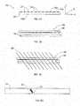
- Figs. 3A - 3DThe simplest example of concurrent manufacture of multiple bodies for LOEs, where each LOEs includes a single light directing region, is shown in Figs. 3A - 3D ; and more practical examples for concurrent manufacture of multiple LOE's bodies where each LOE includes an array of two or more light directing surfaces 22 arranged in an X-Z plane in a spaced-apart parallel relationship along one of the X-axis and Z-axis (the light directing regions may be elongated extending along the Z-axis) are described below with reference to Figs. 4A- 4E, 5A-5G and 6A-6F.
- a patterned substrate 70is prepared.
- the patterned substrate 70has an optically transparent planar body 20 with at least one surface pattern 72A on at least one of its surfaces 70A. It should be understood, although not specifically shown, that the opposite surface 70B may also be provided with a surface pattern.
- the pattern 72Ais in the form of an array of spaced apart, parallel, light directing regions 22 (generally at least two such regions) spaced by optically transparent regions 74 of the substrate 20.
- the regions 22 and 74are, respectively, coated by desired light directing material (e.g. at least partially reflective or diffractive) and uncoated regions.
- the light directing regions 22 in this exampleare elongated extending along the Z-axis, and are arranged in a spaced-apart relationship along the X-axis with optically transparent uncoated regions 74 between them.
- the surface pattern 72Amay be created using any known suitable techniques, such as lithography (negative or positive), direct writing, etc., following or preceding with an optical coating process.
- the light directing regions 22may be arranged in a two-dimensional array, i.e. light directing regions may be spaced apart along both the X- and Z-axes.
- a multi-layer stack 80is created, by gluing with an optical adhesive, including optically transparent layers (substrates) 20, 76 stacked one on top of the other along the Y-axis, where the pattern 72A of the light directing regions 22 is located at an interface 50 between the layers.
- the configurationmay be such that another surface pattern is made on surface 70B and is thus located at an interface between surface 70B and the other optically transparent layer 76.
- a dicing / cuttingis applied to the stack 80 ( Fig . 3C ) along dicing planes 82 which intersect with the X-Z plane at predetermined angle and pass through the optically transparent uncoated regions 74.
- a plurality of LOE's bodies 20are fabricated - 11 such bodies in the present example, only one of which being shown in Fig. 3D .
- Each such LOEhas one light directing region 22 fully embedded in the LOE's body 20 and forming said angle with the major surfaces.
- such LOEhas no internal interfaces other than interface 50 which is located in a plane parallel to the light directing surface 22 and said light directing surface is located on a region of the interface 50 while being spaced from the outer surfaces of the body 22.
- a various coatingsincluding, but not limited to, Hard Coating (HC), Anti-scratch coating, super-hydrophobic coating, anti-smudge coating, anti-bacterial and anti-fouling coating, Anti-reflection coating, to create the major reflective surfaces of the LOE.
- Methods for the creating these coatingsmay include but are not limited to, liquid/solvent based coating such as dip coating, spin coating, spray-coating, die coating, capillary coating, roll coating, curtain/knife coating, bar-coating, or various printing technique, and may further include a curing step (e.g. UV/Electron beam/Thermal curing) and an additional polishing step.
- the method of the inventioncan advantageously be used for concurrent manufacture of a large number of LOEs, each including an array of light directing surfaces.
- One of such methodis exemplified in Figs. 4A-4E .
- the methodstarts from preparation of the patterned substrates 70 ( Fig. 4A ) generally similar to the substrate of Fig. 3A .
- the substratesare prepared using any known suitable patterning technique.
- the patterned substrates 70are optically bonded along the Y-axis with an optical adhesive in an aligned manner one on top of the other ( Fig. 4B ), and may be enclosed between top and bottom optically transparent layers or only uppermost patterned surface may be covered by an optically transparent layer.
- a multi-layer stack 80is fabricated.
- the patterns 72are located at interfaces between the adjacent layers.
- the patterns 72 located in different planesare shifted with respect to one another along the X-axis with a predetermined shift value ⁇ x.
- the shift value ⁇ xis smaller than the minimal X-dimension, X uncoat , of the uncoated optically transparent region 74 between the adjacent light directing regions 22 in the layer.
- Such shifted-patterns' configurationcan be obtained by either preparing the patterned layers with the required shift of the patterns, or by stacking the similarly patterned layers with the required lateral shift.
- the above-described dicing / cutting processis applied to the multi-layer stack 80 ( Figs. 4C and 4D ) along dicing planes 82 which intersect with the X-Z plane forming a predetermined angle ⁇ with the X-Z plane (as shown in Fig. 4D ) and pass through the spacer regions 74 in all the patterned layers.
- This processresults in the multiple LOE's bodies, each configured as shown in Fig. 4E , being formed with the multiple light directing regions 22 all fully embedded in the body 20 such that they are spaced from the major surfaces and are oriented with the angle ⁇ with respect to the major surfaces.
- the edge cutting processcan be applied, either to the entire stack 80, or separately to each LOE body resulting from the dicing process.
- the dimensions of the spacer/uncoated regions 74 between the light directing regions 22, as well as the parameters of the dicing applied to the stack,define distance(s) of the light directing regions 22 from the major surfaces of the LOE.
- the configurationmay be such that the light directing regions 22 in the LOE 20 include regions of the same or different dimensions, as well as regions that are equally or differently spaced from the major surfaces.
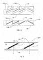
- Figs. 5A to 5Gshow another example of a method of the invention for fabrication of the multiple LOEs, each having an array of light directing regions.
- multiple patterned substratesare prepared, one such patterned substrate 70 being shown in Fig. 5A .
- the patterned substratehas an optically transparent planar body 20 with a surface pattern 72A on at least one surfaces 70A.
- the opposite surface of the substratemay also be provided with a surface pattern.
- the pattern 72Ais in the form of two or more spaced apart, parallel, light directing regions 22 (regions coated with the required light redirecting material, such as reflective, partially reflective, or diffractive material) spaced by optically transparent (uncoated) regions 74 along the X-axis.
- the light directing 22 regionsare elongated (lines) extend along the Z-axis.
- the surface pattern 72Amay be created using any known suitable techniques, such as lithography (negative or positive), direct writing, etc., following or preceding with an optical coating process.
- patterned substrates 70are prepared to be enclosed between top and bottom optically transparent layers/plates 76 ( Fig. 5B ).
- the patterned substrates 70are then stacked using an optical adhesive in an aligned manner one on top of the other along the Y-axis ( Fig. 5C ), and enclosed between the top and bottom optically transparent unpatterned plates 76 (or only the uppermost patterned surface may be covered by an optically transparent plate 76 ).
- a multi-layer stack 80is fabricated.
- the patterns 72light directing regions
- the substratesare shifted with respect to one another along the Z-axis with a predetermined shift value ⁇ z .
- FIG. 5DA dicing / cutting process being applied to the multi-layer stack 80 is shown in Fig. 5D .
- the dicing planes 82intersect with the X-Z plane forming a predetermined angle with the X-Z plane (as described above with reference to Fig. 4D ).
- This processresults in multiple LOE substrates - one such substrate 20 being shown in Fig. 5E .
- This substratehas two arrays 78A and 78B of light directing regions embedded therein (generally, two or more arrays, depending on the pattern in each initial substrate 70 ), where the light directing regions in the array are arranged in a spaced-apart relationship along the Z-axis, and the two arrays are arranged with a space 84 between them along the X-axis.
- a further dicing/cutting stagemay optionally be applied to the space region 84 in such multi-array substrate ( Fig. 5F ), in order to obtain two LOE bodies 20A and 20B, containing respectively arrays 76A and 76B of the embedded light directing regions. As shown in Fig.
- each of the so-obtained LOE's substrates/bodiesfurther undergoes edge cutting and polishing.
- the light directing regions 22are located within interfaces 50 oriented at the angle ⁇ with respect to major surface 26 and 28, and regions 22 are appropriately spaced from the major surfaces.
- Fig. 5Fcan alternatively be applied to the entire stack 80 of Fig. 5C , prior to the dicing process exemplified in Fig. 5D (i.e. dicing along planes 82 ).
- the dicing of Fig. 5Dwould be applied twice, separately to the each of two so-obtained single-array stacks.
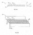
- FIG. 6A to 6Fshowing yet further example of a method of the invention for concurrent fabrication of the multiple LOEs, each with multiple light directing regions. This example is actually an alternative to that of Figs. 5A-5G .
- Fig. 6Ashows one of a multiple patterned substrates 70.
- a patterned surface (generally, at least one surface) of the substrate 70has a pattern in the form of a two-dimensional array of light directing regions arranged in a spaced-apart relationship along both the X-axis and the Z-axis.
- the light directing regionsare coated by desired light directing material and are spaced by uncoated regions of the substrate.
- the patternmay be described as being formed by two arrays 72A and 72B of regions 22, where the arrays are spaced along the Z-axis, and the regions 22 of each array are spaced-apart along the X-axis.
- Multiple patterned substrates 70are prepared and put one on top of the other such that the patterns of different substrates are shifted with respect to one another along the X-axis a predetermined shift value ⁇ x , as shown in Fig. 6B .
- the shift value ⁇ xis smaller than the minimal X-dimension, X uncoat , of the uncoated optically transparent region 74 between the adjacent light directing regions 22 in the layer. It should be understood that in order to obtain such shift between the patterns, either the initially prepared substrates have shifted patterns, or the similarly patterned substrates are stacked with such shift, or both techniques are used.
- the patterned substratesare optically bonded with an optical adhesive in an aligned manner one on top of the other to form a stack 80 ( Fig. 6C ), and may be enclosed between top and bottom optically transparent layers 76 (or only covered by the uppermost layer).
- the patternsare located at interfaces 50 between the adjacent layers/substrates.
- a dicing / cutting processis applied to the multi-layer stack 80 ( Fig. 6D ) along dicing planes 82 which intersect with the X-Z plane forming a predetermined angle ⁇ therewith as described above.
- the resulting LOE body 20, being one of the multiple bodies,is shown in Fig. 6E , and after the edge cutting and polishing process - is shown in Fig. 6F .
- the dicing/cutting along the X-axis in the space between the two arraysmight be first applied to the stack 80 and then the dicing along planes 82 may be applied to each of the resulting half-stacks.
- Each LOE body 20has multiple spaced-apart parallel light directing regions all fully embedded in the body such that they are spaced (equally or not) from the surfaces 26 and 28 that are to serve as major surfaces.
- the LOE produced by the methods of the inventionhas no internal interfaces other than interfaces 50 which are located in a plane parallel to the light directing surface 22 and said light directing surfaces are located in regions of the interfaces 50, while being spaced from the surfaces of the body 22 to be used as the major reflective surfaces.
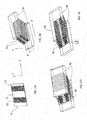
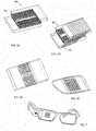
- Fig. 7exemplifies how the structure (LOE) of the invention can be incorporated in spectacles.
- Each lens in the spectaclesis formed as or carries the LOE attached thereto, and, when used together with a virtual image source, the light directing surfaces directs virtual image light towards the wearer's eye.
Landscapes
- Physics & Mathematics (AREA)
- General Physics & Mathematics (AREA)
- Optics & Photonics (AREA)
- Engineering & Computer Science (AREA)
- Manufacturing & Machinery (AREA)
- Optical Elements Other Than Lenses (AREA)
- Light Guides In General And Applications Therefor (AREA)
Abstract
Description
- The present invention is in the field of optical devices and relates to a compact light-guide optical element and a method of its manufacture. More specifically, the present invention relates to a substrate-guided optical device including one or more at least partially reflecting or diffractive surfaces carried by a common light-transmissive substrate.
- Such light-guide optical element (LOE) can be used in a large number of imaging applications, such as portable DVDs, cellular phone, mobile TV receiver, video games, portable media players, or any other mobile display devices, e.g. see-through near-eye display, or head-mounted display, for use in augmented/virtual reality systems. The main physical principle of the operation of LOE is that light waves are trapped inside a substrate by total internal reflections from the major surfaces of the LOE. In addition, the light waves which are trapped inside the LOE are coupled out into the eyes of the viewer by one or more internal reflecting or partially reflecting / diffractive surfaces.
- One of the important factors defining the performance of the above-described LOE is associated with a requirement for uniformity of illumination formed by light output from the LOE. To this end, the actual active area of each partially reflecting surface is to be considered, because a potential non-uniformity in the resulting image might occur due to the different reflection sequences of different rays that reach each selectively reflecting surfaces. More specifically, some rays arrive without previous interaction with a selectively reflecting surface; while other rays arrive after one or more partial reflections.
- Since the inactive portions of the selectively reflecting surfaces do not contribute to the coupling of the trapped light waves out of the substrate, their impact on the optical performance of the LOE can be only negative. That is, if there is no overlapping between the reflecting surfaces then there will be inactive optical portions in the output aperture of the system and "holes" will exist in the image. On the other hand, the inactive portions of the reflecting surfaces are certainly active with respect to the light waves from the external scene. In addition, the major axis orientation of two adjacent surfaces cannot be identical; otherwise the entire second surface will be inactive. Therefore, if overlapping is set between the reflective surfaces to compensate for the inactive portions in the output aperture then rays from the output scene that cross these overlapped areas will suffer from double attenuations and holes will be created in the external scene. This phenomenon significantly reduces the performance not only of displays, which are located at a distance from the eye like head-up displays, but that of near-eye displays also.
- The above problem, and some solutions therefor, are described for example in
US 7,724,443 andWO 2007/054928 , both assigned to the assignee of the present application. The possible technique to overcome the problem is by providing that only the actual active portions of the partially reflecting surfaces are embedded inside the substrate, that is, the reflecting surfaces do not intersect with the lower major surface, but terminate short of this surface. Since the ends of the reflecting surfaces are adjacent to one another over the length of the LOE, there is no holes in the projected augmented image, and since there is no overlap between the surfaces there is no holes in the real image of the external view, thus providing uniform illumination. - There is need in the art for a novel approach for the fabrication of light guide elements (LOEs) of the kind described above, namely LOEs configured for trapping light inside a substrate by total internal reflections from the major surfaces of the LOE, and carrying one or more reflecting or partially reflecting / diffractive surfaces for coupling the trapped light out of the substrate.
- Such LOE and light propagation scheme therein and out thereof is generally illustrated in
Fig. 1A . The LOE20 has a light input region21 (e.g. being aligned with an output of a virtual image source),major surfaces diffractive surfaces 22 arranged with proper orientation inside the LOE. After several reflections from themajor surfaces pupil 25 of viewer's eye24. - Generally speaking such at least partially reflective /
diffractive surface 22 embedded in the LOE's substrate serves for redirecting the light propagating in a general propagation direction through the substrate in one or more output directions. For simplicity, such surface is termed herein below as"light directing surface". - As known, for example from the above-indicated
US 7,724,443 andWO 2007/054928 assigned to the assignee of the present application, the high performance (e.g. uniform illumination) of the LOE can be provided by embedding suchlight directing surfaces 22 in the substrate such that they are spaced from the major surface(s)26, 28. - As schematically shown in
Fig. 1B , according to some of the techniques described in these patent publications, such configuration can be achieved by attaching a blank plate132 (i.e. a plate with no partially reflecting surfaces) to one of the major surfaces of the light guide substrate130 (e.g. by using optical cement), so as to yield at anLOE 134 with the appropriate active apertures for all of the reflecting surfaces. As noted above, the two major surfaces,26 and28, are parallel to each other in such a way that the combined structure forms a complete rectangular parallelepiped. - As shown schematically in
Fig. 1C , according to alternative techniques known from these patent publications, the same can be achieved by fabricating two similar, tooth-shapedtransparent forms 140 fabricated by injection-molding or casting. The required reflecting surfaces22 (either anisotropic or coated thin-film) are inserted in the appropriate places between theforms 140 and the two forms are then glued together to create the required LOE144. - As seen in the figures, the resulting structure134 (
Fig. 1B ) hasinterface 50 located in a plane parallel to the major surfaces and thus inclined with respect to thereflecting surfaces 22; and the resulting structure144 (Fig. 1C ) has aninterface 150 having regions /segments 150A located in planes substantially parallel to the reflectingsurfaces 22 and regions /segments 150B located in planes intersecting those of the reflecting surfaces and the major surfaces. - Generally, in order to achieve an undistorted image having good optical quality, the major and the (partially) reflecting / diffractive surfaces should have high quality. On the other hand, it is desired that the fabrication process of such LOE is as simple and straightforward as possible, as well as cost effective.
- The present invention provides a novel approach for the fabrication of an LOE with one or more at least partially reflecting/diffractive surfaces (at times referred to herein below as "light directing surfaces") coupling light out of the LOE's substrate/body, and a resulting novel configuration of the LOE.
- Thus, according to one broad aspect of the invention, it provides a light guide optical element (LOE) comprising: an optically transparent body which has major surfaces for guiding input light in a general propagation direction through the body by total internal reflections of light from said major surfaces, and carries at least one light directing surface, each light directing surface being configured for coupling the input light out of the body towards one or more output directions. The configuration is such that each of said at least one light directing surface is fully embedded in a volume of said body such that it is spaced from the major surfaces; and the body comprises one or more interfaces inside the body, where all of said one or more interfaces inside the body are located in at least one plane parallel to each of said at least one light directing surface and inclined with respect to said major surfaces at a predetermined angle, said at least one light directing surface being located in at least one region, respectively, at one of said one or more interfaces.
- It should be understood, that in the LOE of the invention there are no interfaces other than those parallel to the light directing surfaces and extending between the major surfaces, and all the light directing surfaces are arranged in regions of at least some of such interfaces. In this connection, it should be understood that the term"interface" used herein refers to a physical boundary between elements forming an integral structure of the LOE.
- In some embodiments, the body (substrate) of the LOE comprises an inner pattern formed by an array of two or more of the light directing surfaces arranged in a spaced-apart parallel relationship along at least one axis. The light directing surfaces of the array are located at the one or more interfaces inside the body and are fully embedded in the volume thereof such that the two or more light directing surfaces are spaced from the major surfaces.
- At least some of such multiple light directing surfaces may be substantially equally spaced from the at least one of the major surfaces; as well as at least some of the multiple light directing surfaces may be of different or same dimensions, while differently spaced from the major surfaces.
- It also should be noted that, although the invention is described below as using light directing surfaces being at least partially reflective / diffractive with respect to the input light propagating in the body, the principles of the invention are not limited to these specific applications. Thus, generally, the light directing surfaces have optical properties different from their surroundings, and may generally include surfaces having different optical properties differently affecting the input light propagating though the body (e.g. inducing polarization effect, spectral effect, etc.).
- In some embodiments, the multiple light directing surfaces of the LOE are arranged in a spaced-apart relationship along two perpendicular axes in said at least one plane.
- The present invention provides a novel method for fabricating the above-described LOE. Moreover, the method of the invention is advantageous for mass production of such LOEs, as is provides a simple technique for concurrently manufacturing multiple LOEs using any known suitable patterning technique(s).
- Thus, according to another broad aspect of the invention, it provides a method for fabrication of two or more light guide optical elements (LOEs) configured as described above, the method comprising:
- preparing at least one patterned substrate, the patterned substrate having an optically transparent planar body with a surface thereof formed with a pattern of spaced apart, parallel, light directing regions, which are arranged in an X-Z plane in a spaced-apart relationship along one of X-axis and Z-axis with optically transparent spacer regions between them;
- enclosing said at least one patterned substrate between top and bottom optically transparent substrates, thereby forming a stack of multiple optically transparent layers stacked one on top of the other along Y-axis, where the pattern of the spaced apart, parallel, light directing regions is located at an interface between the layers;
- dicing said stack of multiple optically transparent layers along a dicing plane intersecting with the X-Z plane and forming a predetermined angle with the X-Z plane, into a predetermined number of slices spaced from one another along the X-axis, to thereby define a plurality of bodies for the LOEs, each of said bodies comprising the at least one light directing region which is fully embedded in the LOE's body such that said at least one light directing region is spaced from major surfaces of the LOE and forms with said major surfaces said predetermined angle.
- The method further comprises applying edge cutting to each of said slices producing the LOE having the optically transparent body having major surface and comprising the at least one light directing surface embedded in the body spaced from the major surfaces.
- In some embodiments, where each of the LOEs to be fabricated should include multiple light directing regions, more than one patterned substrates are provided being placed one on top of the other along the Y-axis and being all enclosed between the top and bottom layers, such that the patterns of said patterned substrates are located at interfaces between the adjacent layers and are shifted with respect to one another along one of X-axis and Z-axis, thereby forming said plurality of the LOEs, each LOE comprising an inner pattern comprising two or more spaced-apart light directing regions fully embedded in the body.
- It should be noted that, in some embodiments, the shift value is smaller than a minimal spacer/uncoated region between the adjacent light directing regions in the layer.
- The above shift of the patterns in the adjacent layers can be achieved by properly applying the patterning process; or by shifting the similarly patterned substrates with respect to one another along X-axis.
- The dimensions of the spacer regions and the dicing of the stack into the slices define distance(s) of the light directing region(s) from the major surfaces of the LOE. The two or more light directing regions may include regions of different dimensions, as well as may include regions having different optical properties differently affecting the input light.
- The patterned layers may be of the same or different thicknesses.
- As indicated above, the patterned substrate may be prepared by any known suitable technique, e.g. a lithography process (negative or positive patterning) creating the pattern of the spaced apart, parallel, light directing regions spaced by optically transparent spacer regions; or applying to a surface of the optically transparent planar body a direct writing patterning process.
- It should be understood that, in some cases, an intermediate structure formed by the above-described stack of multiple optically transparent layers where one or more of the layers have the surface pattern, can be produced, and supplied to a customer for further slicing into LOE bodies, when needed.
- The invention, in its yet further broad aspect provides such an optical structure prepared for forming therefrom multiple LOE's bodies. The optical structure is configured as a stack of multiple optically transparent layers, wherein:
- each of said optically transparent layers has a surface pattern of parallel light directing regions which are arranged in an X-Z plane in a spaced-apart relationship along at least X-axis with optically transparent space regions between them;
- the multiple layers are stacked one on top of the other along Y-axis such that each of the surface patterns is located at an interface between two adjacent layers and the patterns of said layers are aligned with a shift of a predetermined value along one of the X-axis and Z-axis,
- thereby enabling dicing of the optical structure, along a dicing plane intersecting with a X-Z plane and forming a predetermined angle with the X-Z plane, into a predetermined number of slices spaced along one of the X-axis and Z-axes, to produce a plurality of bodies for the LOE elements, each of said bodies being formed with an inner pattern comprising an array of spaced-apart, parallel, light directing regions fully embedded in the LOE's body and being inclined with respect to surfaces of the LOE body, configured for major reflecting surfaces, with said predetermined angle.
- As indicated above, the multiple layers may include two or more layers of different thicknesses.
- The light directing regions of the pattern may be arranged in spaced-apart relationship along both the X-axis and Z-axis.
- The invention also provides a light guide optical element (LOE) comprising an optically transparent body comprising major surfaces and configured for guiding input light in a general propagation direction through the body by total internal reflections of light from said major surfaces, and carrying at least one light directing surface configured for coupling said input light out of the body towards one or more output directions and being fully embedded in a volume of said body such that it is spaced from the major surfaces, the LOE being manufactured by a method comprising:
- preparing at least one patterned substrate having an optically transparent planar body with a surface thereof formed with a pattern of spaced apart, parallel, light directing regions, which are arranged in an X-Z plane in a spaced-apart relationship along one of X-axis and Z-axis with optically transparent regions of the substrate between them;
- enclosing said at least one patterned substrate between top and bottom optically transparent substrates, thereby forming a stack of multiple optically transparent layers stacked one on top of the other along Y-axis, where the pattern of the spaced apart, parallel, light directing regions is located at an interface between the layers;
- dicing said stack of multiple optically transparent layers along a dicing plane intersecting with an X-Z plane and forming a predetermined angle with said X-Z plane, into a predetermined number of slices spaced from one another along said one of the X-axis and Z-axis, to thereby define a plurality of bodies for the LOEs, each of said bodies comprising the at least one light directing region which is fully embedded in the LOE's body
- In order to better understand the subject matter that is disclosed herein and to exemplify how it may be carried out in practice, embodiments will now be described, by way of non-limiting examples only, with reference to the accompanying drawings, in which:
Fig. 1A schematically illustrate the configuration and operation of a convention planar light-guide optical element (LOE) of the type to which the present invention relates;Figs. 1B and1C show two known examples of the LOW configuration aimed at solving the problem associated with the conventional LOW configuration ofFig. 1A ;Fig. 2 shows schematically the configuration of the LOE according to the present invention;Figs. 3A - 3D show an example of a method of the invention for fabrication of the multiple LOEs, each configured with a single light directing region embedded in the LOE's body;Figs. 4A - 4E show another example of a method of the invention for fabrication of the multiple LOEs, each configured with a plurality of the spaced-apart light directing regions embedded in the LOE's body, by stacking multiple patterned substrates where the regions in each substrate extend along the Z-axis and are spaced along the X-axis, and the patterns in the stacked substrates are shifted along the X-axis;Fig. 4F exemplifies the LOE fabricated by the general method ofFigs. 4A-D , but using different patterned layers, such that multiple light directing surfaces in the LOE include light directing surfaces having different dimensions and being differently spaced from at least one of the major surfaces;Figs. 5A to 5G show yet another example of a method of the invention for fabrication of the multiple LOEs, each configured with a plurality of the spaced-apart light directing regions embedded in the LOE's body, by stacking multiple patterned substrates where the regions in each substrate extend along the Z-axis and are spaced along the X-axis, and the patterns in the stacked substrates are shifted along the Z-axis;Figs. 6A to 6F show yet further example of a method of the invention for fabrication of the multiple LOEs, each configured with a plurality of the spaced-apart light directing regions embedded in the LOE's body, by stacking multiple patterned substrates where the regions in each substrate extend along the Z-axis and are spaced along both the X-axis and the Z-axis, and the patterns in the stacked layers are shifted along the X-axis; andFig. 7 illustrates a spectacles configured in which the lenses incorporate the LOEs of the invention.- As described above,
Fig. 1A illustrates schematically the configuration and operation (light propagation scheme) in a conventional LOE device, andFigs. 1B and1C show two examples of the improved LOE configuration providing that the light directing surfaces are fully embedded in substrate of the LOE device, being spaced from the major surface(s) thereof. - Reference is now made to
Fig. 2 which schematically illustrates a part of anLOE device 200 configured according to the present invention. To facilitate understanding, the same reference numbers are used for identifying components that are common in all the examples of the invention and those of the known device described above. - The
LOE 200 includes an opticallytransparent body 20 which has twomajor surfaces light directing surface 22. The LOE's is thus configured for guiding input light in a general propagation direction D through thebody 20 by total internal reflections of light from themajor surfaces LOE 200 is configured such that all of the light directing surface(s) 22 are fully embedded in the volume of thebody 20 being spaced (equally or not) from the major surfaces. TheLOE 200 is manufactured such that thebody 20 includes one or more internal interfaces, generally at60, where each internal interface extends between the major surfaces, and where all the interfaces (in the simplest case there may be only one such interface) are located in planes parallel to that/those of the light directing surface(s)22, and the light directing surface(s)22 is/are located in region(s), respectively, such one ormore interfaces 60. - The following are several examples of a fabrication method of the invention for fabricating the LOE device of the invention. The simplest example of concurrent manufacture of multiple bodies for LOEs, where each LOEs includes a single light directing region, is shown in
Figs. 3A - 3D ; and more practical examples for concurrent manufacture of multiple LOE's bodies where each LOE includes an array of two or more light directing surfaces22 arranged in an X-Z plane in a spaced-apart parallel relationship along one of the X-axis and Z-axis (the light directing regions may be elongated extending along the Z-axis) are described below with reference toFigs. 4A- 4E, 5A-5G and 6A-6F. - As shown in
Fig. 3A , a patternedsubstrate 70 is prepared. The patternedsubstrate 70 has an optically transparentplanar body 20 with at least onesurface pattern 72A on at least one of itssurfaces 70A. It should be understood, although not specifically shown, that theopposite surface 70B may also be provided with a surface pattern. Thepattern 72A is in the form of an array of spaced apart, parallel, light directing regions22 (generally at least two such regions) spaced by opticallytransparent regions 74 of thesubstrate 20. Typically, theregions light directing regions 22 in this example are elongated extending along the Z-axis, and are arranged in a spaced-apart relationship along the X-axis with optically transparentuncoated regions 74 between them. Thesurface pattern 72A may be created using any known suitable techniques, such as lithography (negative or positive), direct writing, etc., following or preceding with an optical coating process. - It should be noted, and will described more specifically further below that the
light directing regions 22 may be arranged in a two-dimensional array, i.e. light directing regions may be spaced apart along both the X- and Z-axes. - Then, the patterned
substrate 70 is enclosed between optically transparent layers76 (or at least thepatterned surface 70A is covered by such layer76). Thus, amulti-layer stack 80 is created, by gluing with an optical adhesive, including optically transparent layers (substrates)20, 76 stacked one on top of the other along the Y-axis, where thepattern 72A of thelight directing regions 22 is located at aninterface 50 between the layers. As noted above, the configuration may be such that another surface pattern is made onsurface 70B and is thus located at an interface betweensurface 70B and the other opticallytransparent layer 76. - Then, a dicing / cutting is applied to the stack80 (
Fig.3C ) along dicingplanes 82 which intersect with the X-Z plane at predetermined angle and pass through the optically transparentuncoated regions 74. By this a plurality of LOE'sbodies 20 are fabricated - 11 such bodies in the present example, only one of which being shown inFig. 3D . Each such LOE has onelight directing region 22 fully embedded in the LOE'sbody 20 and forming said angle with the major surfaces. As shown, such LOE has no internal interfaces other thaninterface 50 which is located in a plane parallel to thelight directing surface 22 and said light directing surface is located on a region of theinterface 50 while being spaced from the outer surfaces of thebody 22. - These outer major surfaces may than be further processed by the application of a various coatings including, but not limited to, Hard Coating (HC), Anti-scratch coating, super-hydrophobic coating, anti-smudge coating, anti-bacterial and anti-fouling coating, Anti-reflection coating, to create the major reflective surfaces of the LOE. Methods for the creating these coatings may include but are not limited to, liquid/solvent based coating such as dip coating, spin coating, spray-coating, die coating, capillary coating, roll coating, curtain/knife coating, bar-coating, or various printing technique, and may further include a curing step (e.g. UV/Electron beam/Thermal curing) and an additional polishing step. Alternatively, dry coatings like evaporation or sputtering of optical coatings might be applied. It should also be noted, although not specifically shown here, that an edge cutting process can be applied to each body resulting from the dicing process, thereby producing the LOE of the desired configuration to guiding input light in a general propagation direction by total internal reflections from the major surfaces and coupling light out of the LOE by interaction with the light directing surface.
- As mentioned above, the method of the invention can advantageously be used for concurrent manufacture of a large number of LOEs, each including an array of light directing surfaces. One of such method is exemplified in
Figs. 4A-4E . In this example, the method starts from preparation of the patterned substrates70 (Fig. 4A ) generally similar to the substrate ofFig. 3A . The substrates are prepared using any known suitable patterning technique. - The patterned
substrates 70 are optically bonded along the Y-axis with an optical adhesive in an aligned manner one on top of the other (Fig. 4B ), and may be enclosed between top and bottom optically transparent layers or only uppermost patterned surface may be covered by an optically transparent layer. By this, amulti-layer stack 80 is fabricated. Insuch stack 80, thepatterns 72 are located at interfaces between the adjacent layers. Also, in such stack, thepatterns 72 located in different planes are shifted with respect to one another along the X-axis with a predetermined shift valueΔx. The shift valueΔx is smaller than the minimal X-dimension, Xuncoat, of the uncoated opticallytransparent region 74 between the adjacentlight directing regions 22 in the layer. Such shifted-patterns' configuration can be obtained by either preparing the patterned layers with the required shift of the patterns, or by stacking the similarly patterned layers with the required lateral shift. - Then, the above-described dicing / cutting process is applied to the multi-layer stack 80 (
Figs. 4C and4D ) along dicingplanes 82 which intersect with the X-Z plane forming a predetermined angleθ with the X-Z plane (as shown inFig. 4D ) and pass through thespacer regions 74 in all the patterned layers. This process results in the multiple LOE's bodies, each configured as shown inFig. 4E , being formed with the multiplelight directing regions 22 all fully embedded in thebody 20 such that they are spaced from the major surfaces and are oriented with the angleθ with respect to the major surfaces. Also, the edge cutting process can be applied, either to theentire stack 80, or separately to each LOE body resulting from the dicing process. - It should be understood that the dimensions of the spacer/
uncoated regions 74 between thelight directing regions 22, as well as the parameters of the dicing applied to the stack, define distance(s) of thelight directing regions 22 from the major surfaces of the LOE. As exemplified inFig. 4F , the configuration may be such that thelight directing regions 22 in theLOE 20 include regions of the same or different dimensions, as well as regions that are equally or differently spaced from the major surfaces. Figs. 5A to5G show another example of a method of the invention for fabrication of the multiple LOEs, each having an array of light directing regions. First, multiple patterned substrates are prepared, one suchpatterned substrate 70 being shown inFig. 5A . The patterned substrate has an optically transparentplanar body 20 with asurface pattern 72A on at least onesurfaces 70A. As mentioned above, the opposite surface of the substrate may also be provided with a surface pattern. Thepattern 72A is in the form of two or more spaced apart, parallel, light directing regions22 (regions coated with the required light redirecting material, such as reflective, partially reflective, or diffractive material) spaced by optically transparent (uncoated)regions 74 along the X-axis. In this example, the light directing22 regions are elongated (lines) extend along the Z-axis. Thesurface pattern 72A may be created using any known suitable techniques, such as lithography (negative or positive), direct writing, etc., following or preceding with an optical coating process.- Multiple
patterned substrates 70 are prepared to be enclosed between top and bottom optically transparent layers/plates76 (Fig. 5B ). The patternedsubstrates 70 are then stacked using an optical adhesive in an aligned manner one on top of the other along the Y-axis (Fig. 5C ), and enclosed between the top and bottom optically transparent unpatterned plates76 (or only the uppermost patterned surface may be covered by an optically transparent plate76). By this, amulti-layer stack 80 is fabricated. Insuch stack 80, the patterns72 (light directing regions) are located at theinterfaces 50 between the adjacent layers. Also, insuch stack 80, the substrates are shifted with respect to one another along the Z-axis with a predetermined shift valueΔz. - A dicing / cutting process being applied to the
multi-layer stack 80 is shown inFig. 5D . As shown, the dicing planes82 intersect with the X-Z plane forming a predetermined angle with the X-Z plane (as described above with reference toFig. 4D ). This process results in multiple LOE substrates - onesuch substrate 20 being shown inFig. 5E . This substrate has twoarrays space 84 between them along the X-axis. A further dicing/cutting stage may optionally be applied to thespace region 84 in such multi-array substrate (Fig. 5F ), in order to obtain twoLOE bodies Fig. 5G , each of the so-obtained LOE's substrates/bodies further undergoes edge cutting and polishing. Thelight directing regions 22 are located withininterfaces 50 oriented at the angle θ with respect tomajor surface regions 22 are appropriately spaced from the major surfaces. - It should be understood that the cutting process of
Fig. 5F can alternatively be applied to theentire stack 80 ofFig. 5C , prior to the dicing process exemplified inFig. 5D (i.e. dicing along planes82). In this case, the dicing ofFig. 5D would be applied twice, separately to the each of two so-obtained single-array stacks. - Reference is now made to
Figs. 6A to6F showing yet further example of a method of the invention for concurrent fabrication of the multiple LOEs, each with multiple light directing regions. This example is actually an alternative to that ofFigs. 5A-5G . Fig. 6A shows one of a multiple patternedsubstrates 70. However, in this example, a patterned surface (generally, at least one surface) of thesubstrate 70 has a pattern in the form of a two-dimensional array of light directing regions arranged in a spaced-apart relationship along both the X-axis and the Z-axis. As described above, the light directing regions are coated by desired light directing material and are spaced by uncoated regions of the substrate. Thus, the pattern may be described as being formed by twoarrays regions 22, where the arrays are spaced along the Z-axis, and theregions 22 of each array are spaced-apart along the X-axis.- Multiple
patterned substrates 70 are prepared and put one on top of the other such that the patterns of different substrates are shifted with respect to one another along the X-axis a predetermined shift valueΔx, as shown inFig. 6B . The shift valueΔx is smaller than the minimal X-dimension, Xuncoat, of the uncoated opticallytransparent region 74 between the adjacentlight directing regions 22 in the layer. It should be understood that in order to obtain such shift between the patterns, either the initially prepared substrates have shifted patterns, or the similarly patterned substrates are stacked with such shift, or both techniques are used. - The patterned substrates are optically bonded with an optical adhesive in an aligned manner one on top of the other to form a stack80 (
Fig. 6C ), and may be enclosed between top and bottom optically transparent layers76 (or only covered by the uppermost layer). Insuch stack 80, the patterns (light directing regions22) are located atinterfaces 50 between the adjacent layers/substrates. - A dicing / cutting process, similar to that described above with respect to
Figs. 3C and4C , is applied to the multi-layer stack80 (Fig. 6D ) along dicingplanes 82 which intersect with the X-Z plane forming a predetermined angleθ therewith as described above. The resultingLOE body 20, being one of the multiple bodies, is shown inFig. 6E , and after the edge cutting and polishing process - is shown inFig. 6F . As described above, in this example, the dicing/cutting along the X-axis in the space between the two arrays, might be first applied to thestack 80 and then the dicing alongplanes 82 may be applied to each of the resulting half-stacks. EachLOE body 20 has multiple spaced-apart parallel light directing regions all fully embedded in the body such that they are spaced (equally or not) from thesurfaces - It should be understood that the LOE produced by the methods of the invention (
Figs. 3D ,4E ,5G and6F ) has no internal interfaces other thaninterfaces 50 which are located in a plane parallel to thelight directing surface 22 and said light directing surfaces are located in regions of theinterfaces 50, while being spaced from the surfaces of thebody 22 to be used as the major reflective surfaces. Fig. 7 exemplifies how the structure (LOE) of the invention can be incorporated in spectacles. Each lens in the spectacles is formed as or carries the LOE attached thereto, and, when used together with a virtual image source, the light directing surfaces directs virtual image light towards the wearer's eye.
Claims (15)
- An optical structure used for producing therefrom two or more light guide optical elements (LOEs), configured such that each LOE comprises an optically transparent body for guiding input light in a general propagation direction through the body by total internal reflections of light from major surfaces of the body and comprises light directing surfaces for coupling the input light out of the body in one or more output directions, where the light directing surfaces are fully embedded in a volume of the body being spaced from the major surfaces of the body and are inclined with respect to said major surfaces at a predetermined angle, the optical structure being configured as a stack of multiple optically transparent layers, wherein:each of said optically transparent layers has a surface pattern of parallel regions configured as light directing surfaces which are arranged in an X-Z plane in a spaced-apart relationship along at least X-axis with optically transparent space regions between them;the multiple layers are stacked one on top of the other along a Y-axis such that each of the surface patterns is located at an interface between two adjacent layers and the patterns of said layers are aligned with a shift of a predetermined value along one of the X-axis and Z-axis;such that the optical structure can be divided, by spaced-apart parallel dicing planes intersecting with a X-Z plane and forming a predetermined angle with the X-Z plane, into a predetermined number of slices spaced along said one of the X-axis and Z-axis, configured as a plurality of the optically transparent bodies for the LOE elements, where each of said bodies has an inner pattern comprising an array of the light directing surfaces arranged in the spaced-apart, parallel relationship and being fully embedded in the LOE's body and inclined with respect to major surfaces of the LOE body, defined by said dicing planes, with said predetermined angle.
- A method for fabricating two or more light guide optical elements (LOEs), such that each of said two or more LOEs comprises an optically transparent body for guiding input light in a general propagation direction through the body by total internal reflections of light from major surfaces of the body and comprises at least one light directing surface for coupling the input light out of the body in one or more output directions, where said at least one light directing surface is fully embedded in a volume of the body being spaced from the major surfaces of the body and inclined with respect to said major surfaces at a predetermined angle, the method comprising:preparing at least one patterned substrate, the patterned substrate having an optically transparent planar body with a surface thereof formed with a pattern of spaced apart, parallel regions having light directing surfaces, which are arranged in an X-Z plane in a spaced-apart relationship along one of X-axis and Z-axis with optically transparent spacer regions of the substrate between them;enclosing said at least one patterned substrate between top and bottom optically transparent substrates, thereby forming a stack of multiple optically transparent layers stacked one on top of the other along Y-axis, where the pattern of the spaced apart, parallel, light directing surfaces is located at an interface between the layers;dicing said stack of multiple optically transparent layers along a dicing plane intersecting with an X-Z plane and forming a predetermined angle with said X-Z plane, into a predetermined number of slices spaced from one another along said one of the X-axis and Z-axis, to thereby define a plurality of bodies for the LOEs, each of said bodies comprising the at least one light directing surface which is fully embedded in the LOE's body.
- The method according to claim 2, comprising more than one patterned substrates placed one on top of the other along the Y-axis and being all enclosed between said top and bottom layers, such that the patterns of said patterned substrates are located at interfaces between the adjacent layers and are shifted with respect to one another along one of X-axis and Z-axis, thereby forming said plurality of the LOEs, each LOE comprising an inner pattern comprising two or more spaced-apart light directing surfaces fully embedded in the body.
- The method according to claim 2 or 3, comprising more than one patterned substrates placed one on top of the other along the Y-axis, being all enclosed between said top and bottom layers, wherein the patterned substrates are shifted with respect to one another along X-axis, thereby providing that the patterns of said patterned substrates are shifted with respect to one another along X-axis with a shift value being smaller than a minimal spacer region between the adjacent light directing regions in the layer, thereby forming said plurality of the LOEs, each LOE comprising an inner pattern comprising two or more spaced-apart light directing surfaces fully embedded in the body.
- The method according to any one of claims 2 to 4, wherein dimensions of the spacer regions and the dicing of said stack into the slices defines distance of the light directing surface from the major surfaces of the LOE.
- The method according to any one of claims 2 to 5, wherein the two or more light directing surfaces comprise regions of different dimensions such that they are differently spaced from the major surfaces.
- The method according to any one of claims 2 to 6, wherein the light directing surfaces comprise surfaces directing light by at least one of reflection and diffraction effects.
- The method according to any one of claims 2 to 7, wherein said preparing of the at least one patterned substrate comprises applying to a surface of the optically transparent planar body a lithography process to create said pattern of the spaced apart, parallel, light directing surfaces spaced by optically transparent spacer regions.
- The method according to any one of claims 2 to 8, wherein each of the major surfaces comprises an outer coating including at least one of the following: Hard Coating (HC), Anti-scratch coating, super-hydrophobic coating, anti-smudge coating, anti-bacterial and anti-fouling coating, Anti-reflection coating.
- The method according to claim 9, comprising applying one of the following processes to said outer surfaces to create said major surfaces of the LOE: liquid/solvent based coating; one or more printing techniques; one or more dry coatings.
- The method according to claim 10, wherein said liquid/solvent based coating comprises at least one of the following: dip coating, spin coating, spray-coating, die coating, capillary coating, roll coating, curtain/knife coating, bar-coating.
- The method according to claim 10, wherein said one or more dry coatings comprise at least one of the following: evaporation; and sputtering of optical coatings.
- The method according to claim 10 or 11, further comprising applying a curing processes to the liquid/solvent based coatings or printed coatings on said outer surfaces.
- The method according to claim 13, further comprising applying polishing to the outer surfaces.
- A light guide optical element (LOE) comprising an optically transparent body comprising major surfaces and configured for guiding input light in a general propagation direction through the body by total internal reflections of light from said major surfaces, and carrying at least one light directing surface configured for coupling said input light out of the body towards one or more output directions and being fully embedded in a volume of said body such that it is spaced from the major surfaces, the LOE being manufactured by a method comprising:preparing at least one patterned substrate having an optically transparent planar body with a surface thereof formed with a pattern of spaced apart, parallel, light directing regions, which are arranged in an X-Z plane in a spaced-apart relationship along one of X-axis and Z-axis with optically transparent regions of the substrate between them;enclosing said at least one patterned substrate between top and bottom optically transparent substrates, thereby forming a stack of multiple optically transparent layers stacked one on top of the other along Y-axis, where the pattern of the spaced apart, parallel, light directing regions is located at an interface between the layers;dicing said stack of multiple optically transparent layers along a dicing plane intersecting with an X-Z plane and forming a predetermined angle with said X-Z plane, into a predetermined number of slices spaced from one another along said one of the X-axis and Z-axis, to thereby define a plurality of bodies for the LOEs, each of said bodies comprising the at least one light directing region which is fully embedded in the LOE's body.
Applications Claiming Priority (1)
| Application Number | Priority Date | Filing Date | Title |
|---|---|---|---|
| IL251645AIL251645B (en) | 2017-04-06 | 2017-04-06 | Light-guide optical element and method of its manufacture |
Publications (2)
| Publication Number | Publication Date |
|---|---|
| EP3385774A1true EP3385774A1 (en) | 2018-10-10 |
| EP3385774B1 EP3385774B1 (en) | 2020-12-02 |
Family
ID=61906644
Family Applications (1)
| Application Number | Title | Priority Date | Filing Date |
|---|---|---|---|
| EP18165614.1AActiveEP3385774B1 (en) | 2017-04-06 | 2018-04-04 | Light-guide optical element and method of its manufacture |
Country Status (7)
| Country | Link |
|---|---|
| US (1) | US10895679B2 (en) |
| EP (1) | EP3385774B1 (en) |
| JP (1) | JP6920737B2 (en) |
| KR (1) | KR102326147B1 (en) |
| CN (1) | CN108693596B (en) |
| IL (1) | IL251645B (en) |
| TW (1) | TWI760463B (en) |
Cited By (2)
| Publication number | Priority date | Publication date | Assignee | Title |
|---|---|---|---|---|
| WO2020148665A1 (en)* | 2019-01-15 | 2020-07-23 | Lumus Ltd. | Method of fabricating a symmetric light guide optical element |
| WO2021152602A1 (en) | 2020-02-02 | 2021-08-05 | Lumus Ltd. | Method for producing light-guide optical elements |
Families Citing this family (62)
| Publication number | Priority date | Publication date | Assignee | Title |
|---|---|---|---|---|
| US10073264B2 (en) | 2007-08-03 | 2018-09-11 | Lumus Ltd. | Substrate-guide optical device |
| IL166799A (en) | 2005-02-10 | 2014-09-30 | Lumus Ltd | Substrate-guided optical device utilizing beam splitters |
| US10261321B2 (en) | 2005-11-08 | 2019-04-16 | Lumus Ltd. | Polarizing optical system |
| IL232197B (en) | 2014-04-23 | 2018-04-30 | Lumus Ltd | Compact head-mounted display system |
| IL235642B (en) | 2014-11-11 | 2021-08-31 | Lumus Ltd | Compact head-mounted display system protected by a hyperfine structure |
| IL237337B (en) | 2015-02-19 | 2020-03-31 | Amitai Yaakov | Compact head-mounted display system having uniform image |
| WO2018065975A1 (en) | 2016-10-09 | 2018-04-12 | Lumus Ltd | Aperture multiplier using a rectangular waveguide |
| KR20240160657A (en) | 2016-11-08 | 2024-11-11 | 루머스 리미티드 | Light-guide device with optical cutoff edge and corresponding production methods |
| CN110431467A (en) | 2017-01-28 | 2019-11-08 | 鲁姆斯有限公司 | Augmented reality imaging system |
| CN108738358B (en) | 2017-02-22 | 2021-03-26 | 鲁姆斯有限公司 | Light guide optics |
| CN109416433B (en) | 2017-03-22 | 2021-06-01 | 鲁姆斯有限公司 | Overlapping Reflector Construction |
| IL251645B (en) | 2017-04-06 | 2018-08-30 | Lumus Ltd | Light-guide optical element and method of its manufacture |
| EP4215980A1 (en) | 2017-07-19 | 2023-07-26 | Lumus Ltd. | Lcos illumination via loe |
| US11513352B2 (en) | 2017-09-29 | 2022-11-29 | Lumus Ltd. | Augmented reality display |
| WO2019077614A1 (en) | 2017-10-22 | 2019-04-25 | Lumus Ltd. | ENHANCED REALITY DEVICE MOUNTED ON THE HEAD AND USING AN OPTICAL BENCH |
| WO2019102366A1 (en) | 2017-11-21 | 2019-05-31 | Lumus Ltd. | Optical aperture expansion arrangement for near-eye displays |
| CN111417883B (en) | 2017-12-03 | 2022-06-17 | 鲁姆斯有限公司 | Optical equipment alignment method |
| KR20200102408A (en) | 2018-01-02 | 2020-08-31 | 루머스 리미티드 | Augmented Reality Display with Active Alignment and Corresponding Method |
| US10551544B2 (en) | 2018-01-21 | 2020-02-04 | Lumus Ltd. | Light-guide optical element with multiple-axis internal aperture expansion |
| MY203244A (en) | 2018-04-08 | 2024-06-19 | Lumus Ltd | Optical sample characterization |
| KR102752134B1 (en) | 2018-05-14 | 2025-01-08 | 루머스 리미티드 | Projector configuration with sub-optical aperture for near-eye display and corresponding optical system |
| IL278511B2 (en) | 2018-05-17 | 2025-01-01 | Lumus Ltd | Near-eye display having overlapping projector assemblies |
| IL259518B2 (en) | 2018-05-22 | 2023-04-01 | Lumus Ltd | Optical system and method for improvement of light field uniformity |
| MX2020012512A (en) | 2018-05-23 | 2021-02-16 | Lumus Ltd | Optical system including light-guide optical element with partially-reflective internal surfaces. |
| CN119595595A (en) | 2018-06-21 | 2025-03-11 | 鲁姆斯有限公司 | Technique for measuring refractive index non-uniformity between plates of light-guiding optical element (LOE) |
| US11415812B2 (en) | 2018-06-26 | 2022-08-16 | Lumus Ltd. | Compact collimating optical device and system |
| EP3824335B1 (en) | 2018-07-16 | 2023-10-18 | Lumus Ltd. | Light-guide optical element employing polarized internal reflectors |
| CN112601993A (en) | 2018-08-26 | 2021-04-02 | 鲁姆斯有限公司 | Reflection suppression in near-eye displays |
| CN116184666A (en) | 2018-09-09 | 2023-05-30 | 鲁姆斯有限公司 | Optical system comprising a light-guiding optical element with two-dimensional expansion |
| US11803056B2 (en)* | 2018-09-14 | 2023-10-31 | Apple Inc. | Waveguided display systems |
| TWM642752U (en) | 2018-11-08 | 2023-06-21 | 以色列商魯姆斯有限公司 | Light-guide display with reflector |
| US11947130B2 (en) | 2018-11-08 | 2024-04-02 | Lumus Ltd. | Optical devices and systems with dichroic beamsplitter color combiner |
| JP3226277U (en) | 2018-11-11 | 2020-05-14 | ルムス エルティーディー. | Near eye display with intermediate window |
| JP2020086345A (en)* | 2018-11-30 | 2020-06-04 | セイコーエプソン株式会社 | Light guide device, virtual image display device, and method for manufacturing light guide device |
| MX2021008808A (en) | 2019-01-24 | 2021-08-24 | Lumus Ltd | Optical systems including loe with three stage expansion. |
| WO2020174433A1 (en) | 2019-02-28 | 2020-09-03 | Lumus Ltd. | Compact collimated image projector |
| TWI800657B (en) | 2019-03-12 | 2023-05-01 | 以色列商魯姆斯有限公司 | Image projector |
| CN216434536U (en) | 2019-04-04 | 2022-05-03 | 鲁姆斯有限公司 | Near-eye display |
| EP3956604A4 (en) | 2019-04-15 | 2022-06-08 | Lumus Ltd. | PROCESS FOR MANUFACTURING AN OPTICAL LIGHT GUIDE ELEMENT |
| TWI845670B (en) | 2019-05-06 | 2024-06-21 | 以色列商魯姆斯有限公司 | Transparent lightguide for viewing a scene and a near-eye display |
| US12050327B2 (en)* | 2019-06-04 | 2024-07-30 | Applied Materials, Inc. | Imaging system and method of manufacturing a metalens array |
| CA3137994A1 (en) | 2019-06-27 | 2020-12-30 | Lumus Ltd | Apparatus and methods for eye tracking based on eye imaging via a light-guide optical element |
| KR20220035088A (en) | 2019-07-18 | 2022-03-21 | 루머스 리미티드 | Encapsulated light guide optics |
| WO2021105982A1 (en) | 2019-11-25 | 2021-06-03 | Lumus Ltd. | Method of polishing a surface of a waveguide |
| IL270991B (en) | 2019-11-27 | 2020-07-30 | Lumus Ltd | Lightguide optical element for polarization scrambling |
| TWI884834B (en) | 2019-12-05 | 2025-05-21 | 以色列商魯姆斯有限公司 | Optical device and method of fabricating optical device |
| US11523092B2 (en) | 2019-12-08 | 2022-12-06 | Lumus Ltd. | Optical systems with compact image projector |
| CN114787687B (en) | 2019-12-25 | 2024-07-30 | 鲁姆斯有限公司 | Systems and methods for eye tracking based on redirection of light from the eye using an optical arrangement associated with a light guide optical element |
| CN218848473U (en) | 2020-05-12 | 2023-04-11 | 鲁姆斯有限公司 | Equipment including projection optics and light guides |
| AU2021279462B2 (en)* | 2020-05-24 | 2023-06-08 | Lumus Ltd. | Method of fabrication of compound light-guide optical elements |
| CN115176190B (en)* | 2020-05-24 | 2024-07-09 | 鲁姆斯有限公司 | Composite light guide optical element |
| KR102862830B1 (en) | 2020-07-20 | 2025-09-19 | 어플라이드 머티어리얼스, 인코포레이티드 | Integrated conductive apertures for optical devices |
| AU2021331833A1 (en) | 2020-08-23 | 2023-03-09 | Lumus Ltd. | Optical system for two-dimensional expansion of an image reducing glints and ghosts from the waveguide |
| WO2022044006A1 (en) | 2020-08-26 | 2022-03-03 | Lumus Ltd. | Generation of color images using white light as source |
| DE202021104723U1 (en) | 2020-09-11 | 2021-10-18 | Lumus Ltd. | Image projector coupled to an optical light guide element |
| CN116368413A (en)* | 2020-10-01 | 2023-06-30 | 鲁姆斯有限公司 | Composite light guide optics |
| KR20230148324A (en) | 2021-03-01 | 2023-10-24 | 루머스 리미티드 | Optical system with compact coupling from projector to waveguide |
| KR102676604B1 (en) | 2021-07-04 | 2024-06-18 | 루머스 리미티드 | Display with stacked light guiding elements providing different parts of the field of view |
| WO2024038458A1 (en) | 2022-08-18 | 2024-02-22 | Lumus Ltd. | Image projector with polarizing catadioptric collimator |
| US20240151885A1 (en)* | 2022-11-03 | 2024-05-09 | Rovi Guides, Inc. | Slanted buried diffractive gratings for optical elements of augmented reality and virtual reality displays |
| WO2024154042A1 (en) | 2023-01-17 | 2024-07-25 | Lumus Ltd. | Characterizing optical system performance with a color camera |
| TWI855873B (en)* | 2023-09-22 | 2024-09-11 | 澤米科技股份有限公司 | Light-guide optical element and its manufacturing method |
Citations (5)
| Publication number | Priority date | Publication date | Assignee | Title |
|---|---|---|---|---|
| US6671100B1 (en)* | 1999-10-14 | 2003-12-30 | Stratos Product Development Llc | Virtual imaging system |
| WO2007054928A1 (en) | 2005-11-08 | 2007-05-18 | Lumus Ltd. | Polarizing optical system |
| US7724443B2 (en) | 2005-02-10 | 2010-05-25 | Lumus Ltd. | Substrate-guided optical device utilizing thin transparent layer |
| US8743464B1 (en)* | 2010-11-03 | 2014-06-03 | Google Inc. | Waveguide with embedded mirrors |
| US20160170214A1 (en)* | 2005-02-10 | 2016-06-16 | Lumus Ltd. | Substrate-guide optical device |
Family Cites Families (261)
| Publication number | Priority date | Publication date | Assignee | Title |
|---|---|---|---|---|
| US2748659A (en) | 1951-02-26 | 1956-06-05 | Jenaer Glaswerk Schott & Gen | Light source, searchlight or the like for polarized light |
| US2886911A (en) | 1953-07-23 | 1959-05-19 | George K C Hardesty | Duo-panel edge illumination system |
| US2795069A (en) | 1956-02-07 | 1957-06-11 | George K C Hardesty | Laminated metal-plastic illuminable panel |
| DE1422172B1 (en) | 1961-12-07 | 1970-11-12 | Kopperschmidt & Co Carl W | periscope |
| US3491245A (en) | 1967-04-10 | 1970-01-20 | George K C Hardesty | Guided light display panel |
| DE2057827A1 (en) | 1969-11-24 | 1971-06-03 | Vickers Ltd | Optical arrangement for flattening the image field |
| US3626394A (en) | 1970-04-09 | 1971-12-07 | Magnavox Co | Magneto-optical system |
| US3667621A (en) | 1970-10-20 | 1972-06-06 | Wisconsin Foundry And Machine | Fluid power system for a self-contained unloading unit |
| US3737212A (en) | 1970-12-14 | 1973-06-05 | Gen Electric | Diffraction optics head up display |
| GB1377627A (en) | 1971-09-01 | 1974-12-18 | Rank Organisation Ltd | Beam splitting prisms |
| US3857109A (en) | 1973-11-21 | 1974-12-24 | Us Navy | Longitudinally-pumped two-wavelength lasers |
| US3873209A (en) | 1973-12-10 | 1975-03-25 | Bell Telephone Labor Inc | Measurement of thin films by optical waveguiding technique |
| FR2295436A1 (en) | 1974-12-16 | 1976-07-16 | Radiotechnique Compelec | DIRECTIVE COUPLING DEVICE FOR MULTIMODES OPTICAL FIBERS |
| US3940204A (en) | 1975-01-23 | 1976-02-24 | Hughes Aircraft Company | Optical display systems utilizing holographic lenses |
| US3969023A (en) | 1975-03-06 | 1976-07-13 | American Optical Corporation | Method and apparatus for detecting layers of stress in lenses |
| US4084883A (en) | 1977-02-28 | 1978-04-18 | The University Of Rochester | Reflective polarization retarder and laser apparatus utilizing same |
| DE3000402A1 (en) | 1979-01-19 | 1980-07-31 | Smiths Industries Ltd | DISPLAY DEVICE |
| US4355864A (en) | 1980-03-26 | 1982-10-26 | Sperry Corporation | Magnetooptic switching devices |
| US4331387A (en) | 1980-07-03 | 1982-05-25 | Westinghouse Electric Corp. | Electro-optical modulator for randomly polarized light |
| FR2496905A1 (en) | 1980-12-24 | 1982-06-25 | France Etat | EPISCOPE WITH MULTIMODES REFLECTIONS |
| DE3266408D1 (en) | 1981-10-14 | 1985-10-24 | Gec Avionics | Optical arrangements for head-up displays and night vision goggles |
| US4516828A (en) | 1982-05-03 | 1985-05-14 | General Motors Corporation | Duplex communication on a single optical fiber |
| FR2562273B1 (en) | 1984-03-27 | 1986-08-08 | France Etat Armement | DEVICE FOR OBSERVING THROUGH A WALL IN TWO OPPOSITE DIRECTIONS |
| US4715684A (en) | 1984-06-20 | 1987-12-29 | Hughes Aircraft Company | Optical system for three color liquid crystal light valve image projection system |
| US4711512A (en) | 1985-07-12 | 1987-12-08 | Environmental Research Institute Of Michigan | Compact head-up display |
| US4805988A (en) | 1987-07-24 | 1989-02-21 | Nelson Dones | Personal video viewing device |
| US4798448A (en) | 1988-02-16 | 1989-01-17 | General Electric Company | High efficiency illumination system for display devices |
| US4932743A (en) | 1988-04-18 | 1990-06-12 | Ricoh Company, Ltd. | Optical waveguide device |
| GB2220081A (en) | 1988-06-21 | 1989-12-28 | Hall & Watts Defence Optics Lt | Periscope apparatus |
| EP0365406B1 (en) | 1988-10-21 | 1993-09-29 | Thomson-Csf | Optical collimating system for a helmet visual |
| FR2638242B1 (en) | 1988-10-21 | 1991-09-20 | Thomson Csf | OPTICAL COLLIMATION SYSTEM, ESPECIALLY FOR A HELMET VISUAL |
| CN1043203A (en) | 1988-12-02 | 1990-06-20 | 三井石油化学工业株式会社 | Light output control method and device thereof |
| US5880888A (en) | 1989-01-23 | 1999-03-09 | Hughes Aircraft Company | Helmet mounted display system |
| US4978952A (en) | 1989-02-24 | 1990-12-18 | Collimated Displays Incorporated | Flat screen color video display |
| FR2647556B1 (en) | 1989-05-23 | 1993-10-29 | Thomson Csf | OPTICAL DEVICE FOR INTRODUCING A COLLIMATED IMAGE INTO THE VISUAL FIELD OF AN OBSERVER AND HELMET COMPRISING AT LEAST ONE SUCH DEVICE |
| US5157526A (en) | 1990-07-06 | 1992-10-20 | Hitachi, Ltd. | Unabsorbing type polarizer, method for manufacturing the same, polarized light source using the same, and apparatus for liquid crystal display using the same |
| US5096520A (en) | 1990-08-01 | 1992-03-17 | Faris Sades M | Method for producing high efficiency polarizing filters |
| US5751480A (en) | 1991-04-09 | 1998-05-12 | Canon Kabushiki Kaisha | Plate-like polarizing element, a polarizing conversion unit provided with the element, and a projector provided with the unit |
| FR2683918B1 (en) | 1991-11-19 | 1994-09-09 | Thomson Csf | MATERIAL CONSTITUTING A RIFLE SCOPE AND WEAPON USING THE SAME. |
| US5367399A (en) | 1992-02-13 | 1994-11-22 | Holotek Ltd. | Rotationally symmetric dual reflection optical beam scanner and system using same |
| US5383053A (en) | 1992-04-07 | 1995-01-17 | Hughes Aircraft Company | Virtual image display having a high efficiency grid beamsplitter |
| US5301067A (en) | 1992-05-06 | 1994-04-05 | Plx Inc. | High accuracy periscope assembly |
| US5231642A (en) | 1992-05-08 | 1993-07-27 | Spectra Diode Laboratories, Inc. | Semiconductor ring and folded cavity lasers |
| US5369415A (en) | 1992-06-29 | 1994-11-29 | Motorola, Inc. | Direct retinal scan display with planar imager |
| WO1994004892A1 (en) | 1992-08-13 | 1994-03-03 | Maechler Meinrad | Spectroscopic systems for the analysis of small and very small quantities of substances |
| US6144347A (en) | 1992-10-09 | 2000-11-07 | Sony Corporation | Head-mounted image display apparatus |
| US5537173A (en) | 1992-10-23 | 1996-07-16 | Olympus Optical Co., Ltd. | Film winding detecting means for a camera including control means for controlling proper and accurate winding and rewinding of a film |
| IL103900A (en) | 1992-11-26 | 1998-06-15 | Electro Optics Ind Ltd | Optical system |
| JP2777041B2 (en) | 1993-02-12 | 1998-07-16 | 京セラ株式会社 | Watch cover glass |
| DE69432526T2 (en) | 1993-02-26 | 2004-04-01 | Yeda Research And Development Co., Ltd. | OPTICAL HOLOGRAPHIC DEVICES |
| GB2276222B (en) | 1993-03-19 | 1997-01-08 | Geoffrey Shepherd | Fluid control valve |
| US5284417A (en) | 1993-06-07 | 1994-02-08 | Ford Motor Company | Automotive fuel pump with regenerative turbine and long curved vapor channel |
| AU686245B2 (en) | 1993-10-07 | 1998-02-05 | Virtual Vision, Inc. | Binocular head mounted display system |
| US5555329A (en) | 1993-11-05 | 1996-09-10 | Alliesignal Inc. | Light directing optical structure |
| JPH07199236A (en) | 1993-12-28 | 1995-08-04 | Fujitsu Ltd | Optical switch and optical distributor |
| US7262919B1 (en) | 1994-06-13 | 2007-08-28 | Canon Kabushiki Kaisha | Head-up display device with curved optical surface having total reflection |
| FR2721872B1 (en) | 1994-07-01 | 1996-08-02 | Renault | DEVICE FOR IMPROVING THE VISION OF A ROAD SCENE |
| JP3219943B2 (en) | 1994-09-16 | 2001-10-15 | 株式会社東芝 | Planar direct-view display device |
| JPH08114765A (en) | 1994-10-15 | 1996-05-07 | Fujitsu Ltd | Polarization separation / conversion device, polarized illumination device and projection type display device using the same |
| US5650873A (en) | 1995-01-30 | 1997-07-22 | Lockheed Missiles & Space Company, Inc. | Micropolarization apparatus |
| GB9521210D0 (en) | 1995-10-17 | 1996-08-28 | Barr & Stroud Ltd | Display system |
| GB2306741A (en) | 1995-10-24 | 1997-05-07 | Sharp Kk | Illuminator |
| US6404550B1 (en) | 1996-07-25 | 2002-06-11 | Seiko Epson Corporation | Optical element suitable for projection display apparatus |
| US5829854A (en) | 1996-09-26 | 1998-11-03 | Raychem Corporation | Angled color dispersement and recombination prism |
| US5886822A (en) | 1996-10-08 | 1999-03-23 | The Microoptical Corporation | Image combining system for eyeglasses and face masks |
| US6204974B1 (en) | 1996-10-08 | 2001-03-20 | The Microoptical Corporation | Compact image display system for eyeglasses or other head-borne frames |
| JPH10133055A (en) | 1996-10-31 | 1998-05-22 | Sharp Corp | Photocoupler and its production |
| US5919601A (en) | 1996-11-12 | 1999-07-06 | Kodak Polychrome Graphics, Llc | Radiation-sensitive compositions and printing plates |
| US6577411B1 (en) | 1996-11-12 | 2003-06-10 | Planop-Planar Optics Ltd. | Optical system for alternative or simultaneous direction of light originating from two scenes to the eye of a viewer |
| US5724163A (en) | 1996-11-12 | 1998-03-03 | Yariv Ben-Yehuda | Optical system for alternative or simultaneous direction of light originating from two scenes to the eye of a viewer |
| JPH10160961A (en) | 1996-12-03 | 1998-06-19 | Mitsubishi Gas Chem Co Inc | Optical element |
| US6292296B1 (en) | 1997-05-28 | 2001-09-18 | Lg. Philips Lcd Co., Ltd. | Large scale polarizer and polarizer system employing it |
| DE19725262C2 (en) | 1997-06-13 | 1999-08-05 | Vitaly Dr Lissotschenko | Optical beam transformation device |
| EP0925526B1 (en) | 1997-06-16 | 2006-05-17 | Koninklijke Philips Electronics N.V. | Projection device |
| US5883684A (en) | 1997-06-19 | 1999-03-16 | Three-Five Systems, Inc. | Diffusively reflecting shield optically, coupled to backlit lightguide, containing LED's completely surrounded by the shield |
| US5896232A (en) | 1997-08-07 | 1999-04-20 | International Business Machines Corporation | Highly efficient and compact frontlighting for polarization-based reflection light valves |
| RU2124746C1 (en) | 1997-08-11 | 1999-01-10 | Закрытое акционерное общество "Кванта Инвест" | Dichroic polarizer |
| GB2329901A (en) | 1997-09-30 | 1999-04-07 | Reckitt & Colman Inc | Acidic hard surface cleaning and disinfecting compositions |
| US6091548A (en) | 1997-10-01 | 2000-07-18 | Raytheon Company | Optical system with two-stage aberration correction |
| CA2307877C (en) | 1997-10-30 | 2005-08-30 | The Microoptical Corporation | Eyeglass interface system |
| EP1068548B1 (en) | 1998-04-02 | 2003-11-12 | Elop Electro-Optics Industries Ltd. | Holographic optical devices |
| US6222971B1 (en) | 1998-07-17 | 2001-04-24 | David Slobodin | Small inlet optical panel and a method of making a small inlet optical panel |
| JP2000155234A (en) | 1998-11-24 | 2000-06-06 | Nippon Electric Glass Co Ltd | Capillary for optical fiber |
| JP2000187177A (en) | 1998-12-22 | 2000-07-04 | Olympus Optical Co Ltd | Image display device |
| US20050024849A1 (en) | 1999-02-23 | 2005-02-03 | Parker Jeffery R. | Methods of cutting or forming cavities in a substrate for use in making optical films, components or wave guides |
| WO2000063738A1 (en) | 1999-04-21 | 2000-10-26 | U.S. Precision Lens Incorporated | Optical systems for reflective lcd's |
| US6798579B2 (en) | 1999-04-27 | 2004-09-28 | Optical Products Development Corp. | Real imaging system with reduced ghost imaging |
| US6728034B1 (en) | 1999-06-16 | 2004-04-27 | Matsushita Electric Industrial Co., Ltd. | Diffractive optical element that polarizes light and an optical pickup using the same |
| JP3913407B2 (en) | 1999-07-09 | 2007-05-09 | 株式会社リコー | Refractive index distribution measuring apparatus and method |
| US20030063042A1 (en) | 1999-07-29 | 2003-04-03 | Asher A. Friesem | Electronic utility devices incorporating a compact virtual image display |
| JP2001141924A (en) | 1999-11-16 | 2001-05-25 | Matsushita Electric Ind Co Ltd | Demultiplexing element and demultiplexing light receiving element |
| JP3828328B2 (en) | 1999-12-28 | 2006-10-04 | ローム株式会社 | Head mounted display |
| US6421148B2 (en) | 2000-01-07 | 2002-07-16 | Honeywell International Inc. | Volume holographic diffusers |
| EP1688766B1 (en) | 2000-01-28 | 2011-04-27 | Seiko Epson Corporation | Light reflective polarizer and projector using the same |
| US6789910B2 (en) | 2000-04-12 | 2004-09-14 | Semiconductor Energy Laboratory, Co., Ltd. | Illumination apparatus |
| US6362861B1 (en) | 2000-05-02 | 2002-03-26 | Agilent Technologies, Inc. | Microdisplay system |
| IL136248A (en) | 2000-05-21 | 2004-08-31 | Elop Electrooptics Ind Ltd | System and method for varying the transmittance of light through a media |
| ATE473464T1 (en) | 2000-06-05 | 2010-07-15 | Lumus Ltd | OPTICAL BEAM EXPANDER WITH SUBSTRATE LIGHT WAVE GUIDE |
| US6307612B1 (en) | 2000-06-08 | 2001-10-23 | Three-Five Systems, Inc. | Liquid crystal display element having a precisely controlled cell gap and method of making same |
| US6324330B1 (en) | 2000-07-10 | 2001-11-27 | Ultratech Stepper, Inc. | Folded light tunnel apparatus and method |
| KR100514011B1 (en) | 2000-07-24 | 2005-09-13 | 미츠비시 레이온 가부시키가이샤 | Surface illuminant device and prism sheet used therefor |
| KR100388819B1 (en) | 2000-07-31 | 2003-06-25 | 주식회사 대양이앤씨 | Optical System for Head Mount Display |
| US6490104B1 (en) | 2000-09-15 | 2002-12-03 | Three-Five Systems, Inc. | Illumination system for a micro display |
| US6542307B2 (en) | 2000-10-20 | 2003-04-01 | Three-Five Systems, Inc. | Compact near-eye illumination system |
| GB0108838D0 (en) | 2001-04-07 | 2001-05-30 | Cambridge 3D Display Ltd | Far field display |
| JP4772204B2 (en) | 2001-04-13 | 2011-09-14 | オリンパス株式会社 | Observation optical system |
| GB2375188B (en) | 2001-04-30 | 2004-07-21 | Samsung Electronics Co Ltd | Wearable Display Apparatus with Waveguide Having Diagonally Cut End Face |
| KR100813943B1 (en) | 2001-04-30 | 2008-03-14 | 삼성전자주식회사 | Composite Reflective Prism and Optical Pick-up Device |
| GB0112871D0 (en) | 2001-05-26 | 2001-07-18 | Thales Optics Ltd | Improved optical device |
| US6672721B2 (en) | 2001-06-11 | 2004-01-06 | 3M Innovative Properties Company | Projection system having low astigmatism |
| US6690513B2 (en) | 2001-07-03 | 2004-02-10 | Jds Uniphase Corporation | Rhomb interleaver |
| US6791760B2 (en) | 2001-07-24 | 2004-09-14 | Itt Manufacturing Enterprises, Inc. | Planar diffractive relay |
| US6556282B2 (en) | 2001-09-04 | 2003-04-29 | Rosemount Aerospace, Inc. | Combined LOAS and LIDAR system |
| EP1433160A1 (en) | 2001-09-07 | 2004-06-30 | The Microoptical Corporation | Light weight, compact, remountable face-supported electronic display |
| DE10150656C2 (en) | 2001-10-13 | 2003-10-02 | Schott Glas | Reflector for a high pressure gas discharge lamp |
| US6775432B2 (en) | 2001-10-19 | 2004-08-10 | Santanu Basu | Method and apparatus for optical wavelength demultiplexing, multiplexing and routing |
| JP2003140081A (en) | 2001-11-06 | 2003-05-14 | Nikon Corp | Hologram combiner optical system |
| JP2003149643A (en) | 2001-11-16 | 2003-05-21 | Goyo Paper Working Co Ltd | Front light for liquid crystal display |
| FR2834799B1 (en) | 2002-01-11 | 2004-04-16 | Essilor Int | OPHTHALMIC LENS WITH PROJECTION INSERT |
| HRP20020044B1 (en) | 2002-01-16 | 2008-11-30 | Mara-Institut D.O.O. | Indirectly prestressed, concrete, roof-ceiling construction with flat soffit |
| IL148804A (en) | 2002-03-21 | 2007-02-11 | Yaacov Amitai | Optical device |
| DE10216169A1 (en) | 2002-04-12 | 2003-10-30 | Zeiss Carl Jena Gmbh | Arrangement for the polarization of light |
| ITTO20020625A1 (en) | 2002-07-17 | 2004-01-19 | Fiat Ricerche | LIGHT GUIDE FOR "HEAD-MOUNTED" OR "HEAD-UP" TYPE DISPLAY DEVICES |
| EP1418459A1 (en) | 2002-11-08 | 2004-05-12 | 3M Innovative Properties Company | Optical device comprising cubo-octahedral polyhedron as light flux splitter or light diffusing element |
| US20050174641A1 (en) | 2002-11-26 | 2005-08-11 | Jds Uniphase Corporation | Polarization conversion light integrator |
| US20090190890A1 (en) | 2002-12-19 | 2009-07-30 | Freeland Riley S | Fiber optic cable having a dry insert and methods of making the same |
| US7175304B2 (en) | 2003-01-30 | 2007-02-13 | Touchsensor Technologies, Llc | Integrated low profile display |
| US7205960B2 (en) | 2003-02-19 | 2007-04-17 | Mirage Innovations Ltd. | Chromatic planar optic display system |
| US7206133B2 (en) | 2003-05-22 | 2007-04-17 | Optical Research Associates | Light distribution apparatus and methods for illuminating optical systems |
| US20060132914A1 (en) | 2003-06-10 | 2006-06-22 | Victor Weiss | Method and system for displaying an informative image against a background image |
| IL157838A (en) | 2003-09-10 | 2013-05-30 | Yaakov Amitai | High brightness optical device |
| JP2005084522A (en) | 2003-09-10 | 2005-03-31 | Nikon Corp | Combiner optics |
| IL157837A (en) | 2003-09-10 | 2012-12-31 | Yaakov Amitai | Substrate-guided optical device particularly for three-dimensional displays |
| IL157836A (en) | 2003-09-10 | 2009-08-03 | Yaakov Amitai | Optical devices particularly for remote viewing applications |
| KR20050037085A (en) | 2003-10-17 | 2005-04-21 | 삼성전자주식회사 | Light tunnel, illuminating device and projector adopting the same |
| US7430355B2 (en) | 2003-12-08 | 2008-09-30 | University Of Cincinnati | Light emissive signage devices based on lightwave coupling |
| US7101063B2 (en) | 2004-02-05 | 2006-09-05 | Hewlett-Packard Development Company, L.P. | Systems and methods for integrating light |
| JP2005308717A (en) | 2004-03-23 | 2005-11-04 | Shin Etsu Chem Co Ltd | Method and apparatus for measuring core non-circularity of optical fiber preform |
| US7418170B2 (en) | 2004-03-29 | 2008-08-26 | Sony Corporation | Optical device and virtual image display device |
| JP4609160B2 (en) | 2004-05-17 | 2011-01-12 | 株式会社ニコン | Optical element, combiner optical system, and information display device |
| EP1748305A4 (en) | 2004-05-17 | 2009-01-14 | Nikon Corp | Optical element, combiner optical system, and image display unit |
| TWI282017B (en) | 2004-05-28 | 2007-06-01 | Epistar Corp | Planar light device |
| IL162573A (en) | 2004-06-17 | 2013-05-30 | Lumus Ltd | Substrate-guided optical device with very wide aperture |
| IL162572A (en) | 2004-06-17 | 2013-02-28 | Lumus Ltd | High brightness optical device |
| JPWO2006001254A1 (en) | 2004-06-29 | 2008-04-17 | 株式会社ニコン | Image combiner and image display device |
| IL163361A (en) | 2004-08-05 | 2011-06-30 | Lumus Ltd | Optical device for light coupling into a guiding substrate |
| US7706901B2 (en) | 2004-10-01 | 2010-04-27 | Microsoft Corporation | Low latency real-time audio streaming |
| JP2006145644A (en) | 2004-11-17 | 2006-06-08 | Hitachi Ltd | Polarization separator and projection display device using the same |
| US7778508B2 (en) | 2004-12-06 | 2010-08-17 | Nikon Corporation | Image display optical system, image display unit, illuminating optical system, and liquid crystal display unit |
| US20060126181A1 (en) | 2004-12-13 | 2006-06-15 | Nokia Corporation | Method and system for beam expansion in a display device |
| US10073264B2 (en) | 2007-08-03 | 2018-09-11 | Lumus Ltd. | Substrate-guide optical device |
| JP2008533507A (en) | 2005-02-10 | 2008-08-21 | ラマス リミテッド | Substrate guiding optical device especially for vision enhancement optical system |
| EP1848966A1 (en) | 2005-02-17 | 2007-10-31 | Lumus Ltd | Personal navigation system |
| WO2006098097A1 (en) | 2005-03-14 | 2006-09-21 | Nikon Corporation | Image display optical system and image display |
| US8187481B1 (en) | 2005-05-05 | 2012-05-29 | Coho Holdings, Llc | Random texture anti-reflection optical surface treatment |
| US7405881B2 (en) | 2005-05-30 | 2008-07-29 | Konica Minolta Holdings, Inc. | Image display apparatus and head mount display |
| JP5030134B2 (en)* | 2005-08-18 | 2012-09-19 | 株式会社リコー | Polarization conversion element, polarization conversion optical system, and image projection apparatus |
| US9081178B2 (en) | 2005-09-07 | 2015-07-14 | Bae Systems Plc | Projection display for displaying an image to a viewer |
| US10261321B2 (en) | 2005-11-08 | 2019-04-16 | Lumus Ltd. | Polarizing optical system |
| IL173715A0 (en) | 2006-02-14 | 2007-03-08 | Lumus Ltd | Substrate-guided imaging lens |
| JP2007219106A (en) | 2006-02-16 | 2007-08-30 | Konica Minolta Holdings Inc | Optical device for expanding diameter of luminous flux, video display device and head mount display |
| IL174170A (en) | 2006-03-08 | 2015-02-26 | Abraham Aharoni | Device and method for binocular alignment |
| CN200941530Y (en) | 2006-08-08 | 2007-08-29 | 牛建民 | Semiconductor laser speckle generator |
| IL177618A (en) | 2006-08-22 | 2015-02-26 | Lumus Ltd | Substrate- guided optical device |
| US20080151375A1 (en) | 2006-12-26 | 2008-06-26 | Ching-Bin Lin | Light guide means as dually effected by light concentrating and light diffusing |
| JP5191771B2 (en) | 2007-04-04 | 2013-05-08 | パナソニック株式会社 | Surface illumination device and liquid crystal display device using the same |
| US8643948B2 (en) | 2007-04-22 | 2014-02-04 | Lumus Ltd. | Collimating optical device and system |
| US8139944B2 (en) | 2007-05-08 | 2012-03-20 | The Boeing Company | Method and apparatus for clearing an optical channel |
| IL183637A (en) | 2007-06-04 | 2013-06-27 | Zvi Lapidot | Distributed head-mounted display |
| CN101730861A (en) | 2007-07-05 | 2010-06-09 | I2Ic公司 | Light source having transparent layers |
| US7589901B2 (en) | 2007-07-10 | 2009-09-15 | Microvision, Inc. | Substrate-guided relays for use with scanned beam light sources |
| JP2009128565A (en) | 2007-11-22 | 2009-06-11 | Toshiba Corp | Display device, display method, and head-up display |
| FR2925171B1 (en) | 2007-12-13 | 2010-04-16 | Optinvent | OPTICAL GUIDE AND OPTICAL SYSTEM OF EYE VISION |
| WO2009127849A1 (en) | 2008-04-14 | 2009-10-22 | Bae Systems Plc | Improvements in or relating to waveguides |
| WO2010022101A2 (en) | 2008-08-19 | 2010-02-25 | Plextronics, Inc. | Organic light emitting diode lighting devices |
| JP2010060770A (en) | 2008-09-03 | 2010-03-18 | Epson Toyocom Corp | Optical article and method for manufacturing optical article |
| US7949214B2 (en) | 2008-11-06 | 2011-05-24 | Microvision, Inc. | Substrate guided relay with pupil expanding input coupler |
| US8317352B2 (en) | 2008-12-11 | 2012-11-27 | Robert Saccomanno | Non-invasive injection of light into a transparent substrate, such as a window pane through its face |
| EP2373924B2 (en) | 2008-12-12 | 2022-01-05 | BAE Systems PLC | Improvements in or relating to waveguides |
| JP2010170606A (en) | 2009-01-21 | 2010-08-05 | Fujinon Corp | Method of manufacturing prism assembly |
| JP5133925B2 (en) | 2009-03-25 | 2013-01-30 | オリンパス株式会社 | Head-mounted image display device |
| CN102356338B (en) | 2009-04-08 | 2015-03-11 | 国际商业机器公司 | Optical waveguide with embedded light-reflecting feature and method for fabricating the same |
| WO2010124028A2 (en) | 2009-04-21 | 2010-10-28 | Vasylyev Sergiy V | Light collection and illumination systems employing planar waveguide |
| US9335604B2 (en) | 2013-12-11 | 2016-05-10 | Milan Momcilo Popovich | Holographic waveguide display |
| US20100291489A1 (en) | 2009-05-15 | 2010-11-18 | Api Nanofabrication And Research Corp. | Exposure methods for forming patterned layers and apparatus for performing the same |
| TW201115231A (en) | 2009-10-28 | 2011-05-01 | Coretronic Corp | Backlight module |
| JP2011199672A (en) | 2010-03-19 | 2011-10-06 | Seiko Instruments Inc | Glass substrate bonding method, glass assembly, package manufacturing method, package, piezoelectric vibrator, oscillator, electronic device, and radio-controlled timepiece |
| JP5499854B2 (en) | 2010-04-08 | 2014-05-21 | ソニー株式会社 | Optical position adjustment method for head mounted display |
| EP2558893A4 (en)* | 2010-04-16 | 2014-06-11 | Flex Lighting Ii Llc | TEACH COMPRISING A LIGHT GUIDE BASED ON A FILM |
| US9028123B2 (en) | 2010-04-16 | 2015-05-12 | Flex Lighting Ii, Llc | Display illumination device with a film-based lightguide having stacked incident surfaces |
| JP5471986B2 (en)* | 2010-09-07 | 2014-04-16 | 株式会社島津製作所 | Optical component and display device using the same |
| US8649099B2 (en) | 2010-09-13 | 2014-02-11 | Vuzix Corporation | Prismatic multiple waveguide for near-eye display |
| US8666208B1 (en) | 2010-11-05 | 2014-03-04 | Google Inc. | Moldable waveguide with embedded micro structures |
| JP5645631B2 (en) | 2010-12-13 | 2014-12-24 | 三菱電機株式会社 | Wavelength monitor, optical module, and wavelength monitoring method |
| US8939579B2 (en) | 2011-01-28 | 2015-01-27 | Light Prescriptions Innovators, Llc | Autofocusing eyewear, especially for presbyopia correction |
| JP5747538B2 (en) | 2011-02-04 | 2015-07-15 | セイコーエプソン株式会社 | Virtual image display device |
| JP2012252091A (en) | 2011-06-01 | 2012-12-20 | Sony Corp | Display apparatus |
| US8639073B2 (en) | 2011-07-19 | 2014-01-28 | Teraxion Inc. | Fiber coupling technique on a waveguide |
| JP6119091B2 (en) | 2011-09-30 | 2017-04-26 | セイコーエプソン株式会社 | Virtual image display device |
| JP5826597B2 (en) | 2011-10-31 | 2015-12-02 | シャープ株式会社 | Simulated solar irradiation device |
| JP5879973B2 (en) | 2011-11-30 | 2016-03-08 | ソニー株式会社 | Light reflecting member, light beam extending device, image display device, and optical device |
| US8917453B2 (en)* | 2011-12-23 | 2014-12-23 | Microsoft Corporation | Reflective array waveguide |
| US10030846B2 (en) | 2012-02-14 | 2018-07-24 | Svv Technology Innovations, Inc. | Face-lit waveguide illumination systems |
| US8665178B1 (en) | 2012-03-01 | 2014-03-04 | Google, Inc. | Partially-reflective waveguide stack and heads-up display using same |
| US8736963B2 (en) | 2012-03-21 | 2014-05-27 | Microsoft Corporation | Two-dimensional exit-pupil expansion |
| IL219907A (en) | 2012-05-21 | 2017-08-31 | Lumus Ltd | Head-mounted display eyeball tracker integrated system |
| CN104582639A (en) | 2012-05-29 | 2015-04-29 | Nlt-脊椎有限公司 | Laterally deflectable implant |
| US20130321432A1 (en) | 2012-06-01 | 2013-12-05 | QUALCOMM MEMES Technologies, Inc. | Light guide with embedded fresnel reflectors |
| CN115494654B (en) | 2012-06-11 | 2025-08-01 | 奇跃公司 | Multi-depth planar three-dimensional display using waveguide reflector array projector |
| US9671566B2 (en) | 2012-06-11 | 2017-06-06 | Magic Leap, Inc. | Planar waveguide apparatus with diffraction element(s) and system employing same |
| US8913324B2 (en) | 2012-08-07 | 2014-12-16 | Nokia Corporation | Display illumination light guide |
| US9933684B2 (en) | 2012-11-16 | 2018-04-03 | Rockwell Collins, Inc. | Transparent waveguide display providing upper and lower fields of view having a specific light output aperture configuration |
| FR2999301B1 (en)* | 2012-12-12 | 2015-01-09 | Thales Sa | OPTICAL GUIDE OF COLLIMATE IMAGES WITH OPTICAL BEAM DEDOLDER AND OPTICAL DEVICE THEREFOR |
| US8947783B2 (en) | 2013-01-02 | 2015-02-03 | Google Inc. | Optical combiner for near-eye display |
| WO2014109115A1 (en)* | 2013-01-10 | 2014-07-17 | ソニー株式会社 | Image display device, image generating device, and transparent spatial light modulating device |
| JP6065630B2 (en) | 2013-02-13 | 2017-01-25 | セイコーエプソン株式会社 | Virtual image display device |
| DE102013106392B4 (en) | 2013-06-19 | 2017-06-08 | Fraunhofer-Gesellschaft zur Förderung der angewandten Forschung e.V. | Process for producing an antireflection coating |
| US8913865B1 (en)* | 2013-06-27 | 2014-12-16 | Microsoft Corporation | Waveguide including light turning gaps |
| CN105358906A (en) | 2013-07-02 | 2016-02-24 | 3M创新有限公司 | Flat light guide |
| US20150081313A1 (en) | 2013-09-16 | 2015-03-19 | Sunedison Llc | Methods and systems for photovoltaic site installation, commissioining, and provisioning |
| DE102013219625B3 (en) | 2013-09-27 | 2015-01-22 | Carl Zeiss Ag | Spectacle lens for a display device which can be placed on the head of a user and generates an image, and a display device with such a spectacle lens |
| JP6225657B2 (en)* | 2013-11-15 | 2017-11-08 | セイコーエプソン株式会社 | OPTICAL ELEMENT, IMAGE DISPLAY DEVICE, AND MANUFACTURING METHOD THEREOF |
| IL313875A (en) | 2013-11-27 | 2024-08-01 | Magic Leap Inc | Virtual and augmented reality systems and methods |
| JP6287131B2 (en) | 2013-12-02 | 2018-03-07 | セイコーエプソン株式会社 | Virtual image display device |
| US9474902B2 (en)* | 2013-12-31 | 2016-10-25 | Nano Retina Ltd. | Wearable apparatus for delivery of power to a retinal prosthesis |
| US9423552B2 (en) | 2014-02-24 | 2016-08-23 | Google Inc. | Lightguide device with outcoupling structures |
| US9311525B2 (en) | 2014-03-19 | 2016-04-12 | Qualcomm Incorporated | Method and apparatus for establishing connection between electronic devices |
| JP6442149B2 (en) | 2014-03-27 | 2018-12-19 | オリンパス株式会社 | Image display device |
| CN108572449B (en) | 2014-03-31 | 2021-09-14 | 联想(北京)有限公司 | Display device and electronic apparatus |
| DE102014207490B3 (en) | 2014-04-17 | 2015-07-02 | Carl Zeiss Ag | Spectacle lens for a display device to be placed on the head of a user and an image-generating display device and display device with such a spectacle lens |
| IL232197B (en) | 2014-04-23 | 2018-04-30 | Lumus Ltd | Compact head-mounted display system |
| JP6567257B2 (en)* | 2014-06-24 | 2019-08-28 | 旭化成株式会社 | Optical device having spectacle lens, spectacles using the same, and spectacle-type display device |
| IL235642B (en) | 2014-11-11 | 2021-08-31 | Lumus Ltd | Compact head-mounted display system protected by a hyperfine structure |
| SG11201703102VA (en)* | 2014-11-13 | 2017-05-30 | Heptagon Micro Optics Pte Ltd | Manufacture of optical light guides |
| IL236490B (en) | 2014-12-25 | 2021-10-31 | Lumus Ltd | Optical component on a conductive substrate |
| IL236491B (en) | 2014-12-25 | 2020-11-30 | Lumus Ltd | A method for fabricating substrate-guided optical device |
| US20160234485A1 (en) | 2015-02-09 | 2016-08-11 | Steven John Robbins | Display System |
| IL237337B (en) | 2015-02-19 | 2020-03-31 | Amitai Yaakov | Compact head-mounted display system having uniform image |
| CN104977648B (en)* | 2015-06-24 | 2018-03-09 | 武汉华星光电技术有限公司 | Light guide plate, backlight module and display device |
| US10007117B2 (en) | 2015-09-10 | 2018-06-26 | Vuzix Corporation | Imaging light guide with reflective turning array |
| KR20180066166A (en)* | 2015-10-05 | 2018-06-18 | 매직 립, 인코포레이티드 | Microlens collimator for scanning optical fiber in virtual / augmented reality system |
| US10345594B2 (en) | 2015-12-18 | 2019-07-09 | Ostendo Technologies, Inc. | Systems and methods for augmented near-eye wearable displays |
| US10473933B2 (en) | 2016-02-19 | 2019-11-12 | Microsoft Technology Licensing, Llc | Waveguide pupil relay |
| JP6898938B2 (en) | 2016-02-24 | 2021-07-07 | マジック リープ, インコーポレイテッドMagic Leap,Inc. | Polarized beam splitter with low light leakage |
| US20170343810A1 (en) | 2016-05-24 | 2017-11-30 | Osterhout Group, Inc. | Pre-assembled solid optical assembly for head worn computers |
| JP6740366B2 (en) | 2016-05-18 | 2020-08-12 | ルーマス リミテッドLumus Ltd. | Head mount imaging device |
| TWI614527B (en) | 2016-08-18 | 2018-02-11 | 盧姆斯有限公司 | Compact head-mounted display system having uniform image |
| WO2018065975A1 (en) | 2016-10-09 | 2018-04-12 | Lumus Ltd | Aperture multiplier using a rectangular waveguide |
| KR20240160657A (en) | 2016-11-08 | 2024-11-11 | 루머스 리미티드 | Light-guide device with optical cutoff edge and corresponding production methods |
| DE212017000261U1 (en) | 2016-12-02 | 2019-08-05 | Lumus Ltd. | Optical system with compact collimator image projector |
| KR102296369B1 (en) | 2016-12-31 | 2021-09-01 | 루머스 리미티드 | Retinal Imaging-Based Eye Tracker with Light-Guiding Optics |
| WO2018127913A1 (en) | 2017-01-04 | 2018-07-12 | Lumus Ltd. | Optical system for near-eye displays |
| CN108738358B (en) | 2017-02-22 | 2021-03-26 | 鲁姆斯有限公司 | Light guide optics |
| CN109416433B (en) | 2017-03-22 | 2021-06-01 | 鲁姆斯有限公司 | Overlapping Reflector Construction |
| IL251645B (en) | 2017-04-06 | 2018-08-30 | Lumus Ltd | Light-guide optical element and method of its manufacture |
| CN107238928B (en) | 2017-06-09 | 2020-03-06 | 京东方科技集团股份有限公司 | an arrayed waveguide |
| US20190170327A1 (en) | 2017-12-03 | 2019-06-06 | Lumus Ltd. | Optical illuminator device |
| US10506220B2 (en) | 2018-01-02 | 2019-12-10 | Lumus Ltd. | Augmented reality displays with active alignment and corresponding methods |
| US10551544B2 (en) | 2018-01-21 | 2020-02-04 | Lumus Ltd. | Light-guide optical element with multiple-axis internal aperture expansion |
| TWM587757U (en) | 2018-05-27 | 2019-12-11 | 以色列商魯姆斯有限公司 | Substrate-guide based optical systems with field curvature effect |
| US11415812B2 (en) | 2018-06-26 | 2022-08-16 | Lumus Ltd. | Compact collimating optical device and system |
- 2017
- 2017-04-06ILIL251645Apatent/IL251645B/enactiveIP Right Grant
- 2018
- 2018-03-27JPJP2018059499Apatent/JP6920737B2/enactiveActive
- 2018-03-27TWTW107110391Apatent/TWI760463B/enactive
- 2018-03-29USUS15/939,285patent/US10895679B2/enactiveActive
- 2018-04-04EPEP18165614.1Apatent/EP3385774B1/enactiveActive
- 2018-04-06KRKR1020180040640Apatent/KR102326147B1/enactiveActive
- 2018-04-08CNCN201810305751.2Apatent/CN108693596B/enactiveActive
Patent Citations (5)
| Publication number | Priority date | Publication date | Assignee | Title |
|---|---|---|---|---|
| US6671100B1 (en)* | 1999-10-14 | 2003-12-30 | Stratos Product Development Llc | Virtual imaging system |
| US7724443B2 (en) | 2005-02-10 | 2010-05-25 | Lumus Ltd. | Substrate-guided optical device utilizing thin transparent layer |
| US20160170214A1 (en)* | 2005-02-10 | 2016-06-16 | Lumus Ltd. | Substrate-guide optical device |
| WO2007054928A1 (en) | 2005-11-08 | 2007-05-18 | Lumus Ltd. | Polarizing optical system |
| US8743464B1 (en)* | 2010-11-03 | 2014-06-03 | Google Inc. | Waveguide with embedded mirrors |
Cited By (4)
| Publication number | Priority date | Publication date | Assignee | Title |
|---|---|---|---|---|
| WO2020148665A1 (en)* | 2019-01-15 | 2020-07-23 | Lumus Ltd. | Method of fabricating a symmetric light guide optical element |
| CN113260889A (en)* | 2019-01-15 | 2021-08-13 | 鲁姆斯有限公司 | Method for manufacturing symmetrical light guide optical element |
| WO2021152602A1 (en) | 2020-02-02 | 2021-08-05 | Lumus Ltd. | Method for producing light-guide optical elements |
| EP4022218A4 (en)* | 2020-02-02 | 2022-11-23 | Lumus Ltd. | PROCESS FOR MANUFACTURING LIGHT-TRANSDUCING OPTICAL ELEMENTS |
Also Published As
| Publication number | Publication date |
|---|---|
| KR102326147B1 (en) | 2021-11-15 |
| EP3385774B1 (en) | 2020-12-02 |
| KR20180113472A (en) | 2018-10-16 |
| IL251645A0 (en) | 2017-06-29 |
| TWI760463B (en) | 2022-04-11 |
| IL251645B (en) | 2018-08-30 |
| CN108693596B (en) | 2021-10-19 |
| JP6920737B2 (en) | 2021-08-18 |
| CN108693596A (en) | 2018-10-23 |
| US10895679B2 (en) | 2021-01-19 |
| JP2018180529A (en) | 2018-11-15 |
| TW201903475A (en) | 2019-01-16 |
| US20180292599A1 (en) | 2018-10-11 |
Similar Documents
| Publication | Publication Date | Title |
|---|---|---|
| EP3385774B1 (en) | Light-guide optical element and method of its manufacture | |
| JP7684339B2 (en) | Metasurfaces for redirecting light and methods of fabrication | |
| US10877214B2 (en) | Diffraction gratings for beam redirection | |
| JP7736852B2 (en) | Systems and methods for mixed reality | |
| AU2022202338B2 (en) | Multi-layer diffractive eyepiece | |
| US10126482B2 (en) | Lightguide device with outcoupling structures | |
| EP3237961B1 (en) | Method for fabricating a substrate-guided optical device | |
| CN107924103B (en) | Display system with optical elements for in-coupling multiplexed light streams | |
| TWI820285B (en) | Method of fabricating a symmetric light guide optical element | |
| EP3217081A1 (en) | Light guide device and virtual-image display device | |
| CN103135235A (en) | Light reflecting member, light beam extension device, image display device, and optical device | |
| CN116406447A (en) | Image display device and method of manufacturing light guide plate | |
| US11892640B1 (en) | Waveguide combiner with stacked plates | |
| KR20110018756A (en) | 3D image display device including lenticular sheet and method of manufacturing same | |
| JP2004246267A (en) | Optical component mount structure and its manufacturing method |
Legal Events
| Date | Code | Title | Description |
|---|---|---|---|
| PUAI | Public reference made under article 153(3) epc to a published international application that has entered the european phase | Free format text:ORIGINAL CODE: 0009012 | |
| STAA | Information on the status of an ep patent application or granted ep patent | Free format text:STATUS: THE APPLICATION HAS BEEN PUBLISHED | |
| AK | Designated contracting states | Kind code of ref document:A1 Designated state(s):AL AT BE BG CH CY CZ DE DK EE ES FI FR GB GR HR HU IE IS IT LI LT LU LV MC MK MT NL NO PL PT RO RS SE SI SK SM TR | |
| AX | Request for extension of the european patent | Extension state:BA ME | |
| STAA | Information on the status of an ep patent application or granted ep patent | Free format text:STATUS: REQUEST FOR EXAMINATION WAS MADE | |
| 17P | Request for examination filed | Effective date:20190409 | |
| RBV | Designated contracting states (corrected) | Designated state(s):AL AT BE BG CH CY CZ DE DK EE ES FI FR GB GR HR HU IE IS IT LI LT LU LV MC MK MT NL NO PL PT RO RS SE SI SK SM TR | |
| GRAP | Despatch of communication of intention to grant a patent | Free format text:ORIGINAL CODE: EPIDOSNIGR1 | |
| STAA | Information on the status of an ep patent application or granted ep patent | Free format text:STATUS: GRANT OF PATENT IS INTENDED | |
| INTG | Intention to grant announced | Effective date:20200630 | |
| GRAS | Grant fee paid | Free format text:ORIGINAL CODE: EPIDOSNIGR3 | |
| GRAA | (expected) grant | Free format text:ORIGINAL CODE: 0009210 | |
| STAA | Information on the status of an ep patent application or granted ep patent | Free format text:STATUS: THE PATENT HAS BEEN GRANTED | |
| AK | Designated contracting states | Kind code of ref document:B1 Designated state(s):AL AT BE BG CH CY CZ DE DK EE ES FI FR GB GR HR HU IE IS IT LI LT LU LV MC MK MT NL NO PL PT RO RS SE SI SK SM TR | |
| REG | Reference to a national code | Ref country code:GB Ref legal event code:FG4D | |
| REG | Reference to a national code | Ref country code:AT Ref legal event code:REF Ref document number:1341579 Country of ref document:AT Kind code of ref document:T Effective date:20201215 Ref country code:CH Ref legal event code:EP | |
| REG | Reference to a national code | Ref country code:IE Ref legal event code:FG4D | |
| REG | Reference to a national code | Ref country code:DE Ref legal event code:R096 Ref document number:602018010244 Country of ref document:DE | |
| PG25 | Lapsed in a contracting state [announced via postgrant information from national office to epo] | Ref country code:RS Free format text:LAPSE BECAUSE OF FAILURE TO SUBMIT A TRANSLATION OF THE DESCRIPTION OR TO PAY THE FEE WITHIN THE PRESCRIBED TIME-LIMIT Effective date:20201202 Ref country code:FI Free format text:LAPSE BECAUSE OF FAILURE TO SUBMIT A TRANSLATION OF THE DESCRIPTION OR TO PAY THE FEE WITHIN THE PRESCRIBED TIME-LIMIT Effective date:20201202 Ref country code:GR Free format text:LAPSE BECAUSE OF FAILURE TO SUBMIT A TRANSLATION OF THE DESCRIPTION OR TO PAY THE FEE WITHIN THE PRESCRIBED TIME-LIMIT Effective date:20210303 Ref country code:NO Free format text:LAPSE BECAUSE OF FAILURE TO SUBMIT A TRANSLATION OF THE DESCRIPTION OR TO PAY THE FEE WITHIN THE PRESCRIBED TIME-LIMIT Effective date:20210302 | |
| REG | Reference to a national code | Ref country code:NL Ref legal event code:MP Effective date:20201202 | |
| REG | Reference to a national code | Ref country code:AT Ref legal event code:MK05 Ref document number:1341579 Country of ref document:AT Kind code of ref document:T Effective date:20201202 | |
| PG25 | Lapsed in a contracting state [announced via postgrant information from national office to epo] | Ref country code:BG Free format text:LAPSE BECAUSE OF FAILURE TO SUBMIT A TRANSLATION OF THE DESCRIPTION OR TO PAY THE FEE WITHIN THE PRESCRIBED TIME-LIMIT Effective date:20210302 Ref country code:SE Free format text:LAPSE BECAUSE OF FAILURE TO SUBMIT A TRANSLATION OF THE DESCRIPTION OR TO PAY THE FEE WITHIN THE PRESCRIBED TIME-LIMIT Effective date:20201202 Ref country code:LV Free format text:LAPSE BECAUSE OF FAILURE TO SUBMIT A TRANSLATION OF THE DESCRIPTION OR TO PAY THE FEE WITHIN THE PRESCRIBED TIME-LIMIT Effective date:20201202 Ref country code:PL Free format text:LAPSE BECAUSE OF FAILURE TO SUBMIT A TRANSLATION OF THE DESCRIPTION OR TO PAY THE FEE WITHIN THE PRESCRIBED TIME-LIMIT Effective date:20201202 | |
| PG25 | Lapsed in a contracting state [announced via postgrant information from national office to epo] | Ref country code:NL Free format text:LAPSE BECAUSE OF FAILURE TO SUBMIT A TRANSLATION OF THE DESCRIPTION OR TO PAY THE FEE WITHIN THE PRESCRIBED TIME-LIMIT Effective date:20201202 Ref country code:HR Free format text:LAPSE BECAUSE OF FAILURE TO SUBMIT A TRANSLATION OF THE DESCRIPTION OR TO PAY THE FEE WITHIN THE PRESCRIBED TIME-LIMIT Effective date:20201202 | |
| REG | Reference to a national code | Ref country code:LT Ref legal event code:MG9D | |
| PG25 | Lapsed in a contracting state [announced via postgrant information from national office to epo] | Ref country code:EE Free format text:LAPSE BECAUSE OF FAILURE TO SUBMIT A TRANSLATION OF THE DESCRIPTION OR TO PAY THE FEE WITHIN THE PRESCRIBED TIME-LIMIT Effective date:20201202 Ref country code:CZ Free format text:LAPSE BECAUSE OF FAILURE TO SUBMIT A TRANSLATION OF THE DESCRIPTION OR TO PAY THE FEE WITHIN THE PRESCRIBED TIME-LIMIT Effective date:20201202 Ref country code:SM Free format text:LAPSE BECAUSE OF FAILURE TO SUBMIT A TRANSLATION OF THE DESCRIPTION OR TO PAY THE FEE WITHIN THE PRESCRIBED TIME-LIMIT Effective date:20201202 Ref country code:LT Free format text:LAPSE BECAUSE OF FAILURE TO SUBMIT A TRANSLATION OF THE DESCRIPTION OR TO PAY THE FEE WITHIN THE PRESCRIBED TIME-LIMIT Effective date:20201202 Ref country code:PT Free format text:LAPSE BECAUSE OF FAILURE TO SUBMIT A TRANSLATION OF THE DESCRIPTION OR TO PAY THE FEE WITHIN THE PRESCRIBED TIME-LIMIT Effective date:20210405 Ref country code:RO Free format text:LAPSE BECAUSE OF FAILURE TO SUBMIT A TRANSLATION OF THE DESCRIPTION OR TO PAY THE FEE WITHIN THE PRESCRIBED TIME-LIMIT Effective date:20201202 Ref country code:SK Free format text:LAPSE BECAUSE OF FAILURE TO SUBMIT A TRANSLATION OF THE DESCRIPTION OR TO PAY THE FEE WITHIN THE PRESCRIBED TIME-LIMIT Effective date:20201202 | |
| PG25 | Lapsed in a contracting state [announced via postgrant information from national office to epo] | Ref country code:AT Free format text:LAPSE BECAUSE OF FAILURE TO SUBMIT A TRANSLATION OF THE DESCRIPTION OR TO PAY THE FEE WITHIN THE PRESCRIBED TIME-LIMIT Effective date:20201202 | |
| REG | Reference to a national code | Ref country code:DE Ref legal event code:R097 Ref document number:602018010244 Country of ref document:DE | |
| PG25 | Lapsed in a contracting state [announced via postgrant information from national office to epo] | Ref country code:IS Free format text:LAPSE BECAUSE OF FAILURE TO SUBMIT A TRANSLATION OF THE DESCRIPTION OR TO PAY THE FEE WITHIN THE PRESCRIBED TIME-LIMIT Effective date:20210402 | |
| PLBE | No opposition filed within time limit | Free format text:ORIGINAL CODE: 0009261 | |
| STAA | Information on the status of an ep patent application or granted ep patent | Free format text:STATUS: NO OPPOSITION FILED WITHIN TIME LIMIT | |
| PG25 | Lapsed in a contracting state [announced via postgrant information from national office to epo] | Ref country code:IT Free format text:LAPSE BECAUSE OF FAILURE TO SUBMIT A TRANSLATION OF THE DESCRIPTION OR TO PAY THE FEE WITHIN THE PRESCRIBED TIME-LIMIT Effective date:20201202 Ref country code:AL Free format text:LAPSE BECAUSE OF FAILURE TO SUBMIT A TRANSLATION OF THE DESCRIPTION OR TO PAY THE FEE WITHIN THE PRESCRIBED TIME-LIMIT Effective date:20201202 | |
| 26N | No opposition filed | Effective date:20210903 | |
| PG25 | Lapsed in a contracting state [announced via postgrant information from national office to epo] | Ref country code:DK Free format text:LAPSE BECAUSE OF FAILURE TO SUBMIT A TRANSLATION OF THE DESCRIPTION OR TO PAY THE FEE WITHIN THE PRESCRIBED TIME-LIMIT Effective date:20201202 Ref country code:SI Free format text:LAPSE BECAUSE OF FAILURE TO SUBMIT A TRANSLATION OF THE DESCRIPTION OR TO PAY THE FEE WITHIN THE PRESCRIBED TIME-LIMIT Effective date:20201202 Ref country code:MC Free format text:LAPSE BECAUSE OF FAILURE TO SUBMIT A TRANSLATION OF THE DESCRIPTION OR TO PAY THE FEE WITHIN THE PRESCRIBED TIME-LIMIT Effective date:20201202 | |
| PG25 | Lapsed in a contracting state [announced via postgrant information from national office to epo] | Ref country code:LU Free format text:LAPSE BECAUSE OF NON-PAYMENT OF DUE FEES Effective date:20210404 | |
| REG | Reference to a national code | Ref country code:BE Ref legal event code:MM Effective date:20210430 | |
| PG25 | Lapsed in a contracting state [announced via postgrant information from national office to epo] | Ref country code:ES Free format text:LAPSE BECAUSE OF FAILURE TO SUBMIT A TRANSLATION OF THE DESCRIPTION OR TO PAY THE FEE WITHIN THE PRESCRIBED TIME-LIMIT Effective date:20201202 Ref country code:CH Free format text:LAPSE BECAUSE OF NON-PAYMENT OF DUE FEES Effective date:20210430 Ref country code:LI Free format text:LAPSE BECAUSE OF NON-PAYMENT OF DUE FEES Effective date:20210430 | |
| PG25 | Lapsed in a contracting state [announced via postgrant information from national office to epo] | Ref country code:IE Free format text:LAPSE BECAUSE OF NON-PAYMENT OF DUE FEES Effective date:20210404 | |
| PG25 | Lapsed in a contracting state [announced via postgrant information from national office to epo] | Ref country code:IS Free format text:LAPSE BECAUSE OF FAILURE TO SUBMIT A TRANSLATION OF THE DESCRIPTION OR TO PAY THE FEE WITHIN THE PRESCRIBED TIME-LIMIT Effective date:20210402 | |
| PG25 | Lapsed in a contracting state [announced via postgrant information from national office to epo] | Ref country code:BE Free format text:LAPSE BECAUSE OF NON-PAYMENT OF DUE FEES Effective date:20210430 | |
| PG25 | Lapsed in a contracting state [announced via postgrant information from national office to epo] | Ref country code:CY Free format text:LAPSE BECAUSE OF FAILURE TO SUBMIT A TRANSLATION OF THE DESCRIPTION OR TO PAY THE FEE WITHIN THE PRESCRIBED TIME-LIMIT Effective date:20201202 | |
| P01 | Opt-out of the competence of the unified patent court (upc) registered | Effective date:20230527 | |
| PG25 | Lapsed in a contracting state [announced via postgrant information from national office to epo] | Ref country code:HU Free format text:LAPSE BECAUSE OF FAILURE TO SUBMIT A TRANSLATION OF THE DESCRIPTION OR TO PAY THE FEE WITHIN THE PRESCRIBED TIME-LIMIT; INVALID AB INITIO Effective date:20180404 | |
| PG25 | Lapsed in a contracting state [announced via postgrant information from national office to epo] | Ref country code:MK Free format text:LAPSE BECAUSE OF FAILURE TO SUBMIT A TRANSLATION OF THE DESCRIPTION OR TO PAY THE FEE WITHIN THE PRESCRIBED TIME-LIMIT Effective date:20201202 | |
| PG25 | Lapsed in a contracting state [announced via postgrant information from national office to epo] | Ref country code:MT Free format text:LAPSE BECAUSE OF FAILURE TO SUBMIT A TRANSLATION OF THE DESCRIPTION OR TO PAY THE FEE WITHIN THE PRESCRIBED TIME-LIMIT Effective date:20201202 | |
| PGFP | Annual fee paid to national office [announced via postgrant information from national office to epo] | Ref country code:DE Payment date:20250428 Year of fee payment:8 | |
| PGFP | Annual fee paid to national office [announced via postgrant information from national office to epo] | Ref country code:GB Payment date:20250422 Year of fee payment:8 | |
| PGFP | Annual fee paid to national office [announced via postgrant information from national office to epo] | Ref country code:FR Payment date:20250424 Year of fee payment:8 |