EP3368311B1 - Additive manufacturing system - Google Patents
Additive manufacturing systemDownload PDFInfo
- Publication number
- EP3368311B1 EP3368311B1EP16860806.5AEP16860806AEP3368311B1EP 3368311 B1EP3368311 B1EP 3368311B1EP 16860806 AEP16860806 AEP 16860806AEP 3368311 B1EP3368311 B1EP 3368311B1
- Authority
- EP
- European Patent Office
- Prior art keywords
- light
- powder
- energy
- build
- laser
- Prior art date
- Legal status (The legal status is an assumption and is not a legal conclusion. Google has not performed a legal analysis and makes no representation as to the accuracy of the status listed.)
- Active
Links
Images


Classifications
- B—PERFORMING OPERATIONS; TRANSPORTING
- B23—MACHINE TOOLS; METAL-WORKING NOT OTHERWISE PROVIDED FOR
- B23K—SOLDERING OR UNSOLDERING; WELDING; CLADDING OR PLATING BY SOLDERING OR WELDING; CUTTING BY APPLYING HEAT LOCALLY, e.g. FLAME CUTTING; WORKING BY LASER BEAM
- B23K37/00—Auxiliary devices or processes, not specially adapted for a procedure covered by only one of the other main groups of this subclass
- B23K37/04—Auxiliary devices or processes, not specially adapted for a procedure covered by only one of the other main groups of this subclass for holding or positioning work
- B23K37/0408—Auxiliary devices or processes, not specially adapted for a procedure covered by only one of the other main groups of this subclass for holding or positioning work for planar work
- B—PERFORMING OPERATIONS; TRANSPORTING
- B22—CASTING; POWDER METALLURGY
- B22F—WORKING METALLIC POWDER; MANUFACTURE OF ARTICLES FROM METALLIC POWDER; MAKING METALLIC POWDER; APPARATUS OR DEVICES SPECIALLY ADAPTED FOR METALLIC POWDER
- B22F10/00—Additive manufacturing of workpieces or articles from metallic powder
- B22F10/20—Direct sintering or melting
- B22F10/28—Powder bed fusion, e.g. selective laser melting [SLM] or electron beam melting [EBM]
- B—PERFORMING OPERATIONS; TRANSPORTING
- B22—CASTING; POWDER METALLURGY
- B22F—WORKING METALLIC POWDER; MANUFACTURE OF ARTICLES FROM METALLIC POWDER; MAKING METALLIC POWDER; APPARATUS OR DEVICES SPECIALLY ADAPTED FOR METALLIC POWDER
- B22F10/00—Additive manufacturing of workpieces or articles from metallic powder
- B22F10/30—Process control
- B22F10/34—Process control of powder characteristics, e.g. density, oxidation or flowability
- B—PERFORMING OPERATIONS; TRANSPORTING
- B22—CASTING; POWDER METALLURGY
- B22F—WORKING METALLIC POWDER; MANUFACTURE OF ARTICLES FROM METALLIC POWDER; MAKING METALLIC POWDER; APPARATUS OR DEVICES SPECIALLY ADAPTED FOR METALLIC POWDER
- B22F10/00—Additive manufacturing of workpieces or articles from metallic powder
- B22F10/30—Process control
- B22F10/36—Process control of energy beam parameters
- B—PERFORMING OPERATIONS; TRANSPORTING
- B22—CASTING; POWDER METALLURGY
- B22F—WORKING METALLIC POWDER; MANUFACTURE OF ARTICLES FROM METALLIC POWDER; MAKING METALLIC POWDER; APPARATUS OR DEVICES SPECIALLY ADAPTED FOR METALLIC POWDER
- B22F10/00—Additive manufacturing of workpieces or articles from metallic powder
- B22F10/30—Process control
- B22F10/39—Traceability, e.g. incorporating identifier into a workpiece or article
- B—PERFORMING OPERATIONS; TRANSPORTING
- B22—CASTING; POWDER METALLURGY
- B22F—WORKING METALLIC POWDER; MANUFACTURE OF ARTICLES FROM METALLIC POWDER; MAKING METALLIC POWDER; APPARATUS OR DEVICES SPECIALLY ADAPTED FOR METALLIC POWDER
- B22F10/00—Additive manufacturing of workpieces or articles from metallic powder
- B22F10/70—Recycling
- B—PERFORMING OPERATIONS; TRANSPORTING
- B22—CASTING; POWDER METALLURGY
- B22F—WORKING METALLIC POWDER; MANUFACTURE OF ARTICLES FROM METALLIC POWDER; MAKING METALLIC POWDER; APPARATUS OR DEVICES SPECIALLY ADAPTED FOR METALLIC POWDER
- B22F12/00—Apparatus or devices specially adapted for additive manufacturing; Auxiliary means for additive manufacturing; Combinations of additive manufacturing apparatus or devices with other processing apparatus or devices
- B22F12/22—Driving means
- B22F12/226—Driving means for rotary motion
- B—PERFORMING OPERATIONS; TRANSPORTING
- B22—CASTING; POWDER METALLURGY
- B22F—WORKING METALLIC POWDER; MANUFACTURE OF ARTICLES FROM METALLIC POWDER; MAKING METALLIC POWDER; APPARATUS OR DEVICES SPECIALLY ADAPTED FOR METALLIC POWDER
- B22F12/00—Apparatus or devices specially adapted for additive manufacturing; Auxiliary means for additive manufacturing; Combinations of additive manufacturing apparatus or devices with other processing apparatus or devices
- B22F12/30—Platforms or substrates
- B22F12/33—Platforms or substrates translatory in the deposition plane
- B—PERFORMING OPERATIONS; TRANSPORTING
- B22—CASTING; POWDER METALLURGY
- B22F—WORKING METALLIC POWDER; MANUFACTURE OF ARTICLES FROM METALLIC POWDER; MAKING METALLIC POWDER; APPARATUS OR DEVICES SPECIALLY ADAPTED FOR METALLIC POWDER
- B22F12/00—Apparatus or devices specially adapted for additive manufacturing; Auxiliary means for additive manufacturing; Combinations of additive manufacturing apparatus or devices with other processing apparatus or devices
- B22F12/38—Housings, e.g. machine housings
- B—PERFORMING OPERATIONS; TRANSPORTING
- B22—CASTING; POWDER METALLURGY
- B22F—WORKING METALLIC POWDER; MANUFACTURE OF ARTICLES FROM METALLIC POWDER; MAKING METALLIC POWDER; APPARATUS OR DEVICES SPECIALLY ADAPTED FOR METALLIC POWDER
- B22F12/00—Apparatus or devices specially adapted for additive manufacturing; Auxiliary means for additive manufacturing; Combinations of additive manufacturing apparatus or devices with other processing apparatus or devices
- B22F12/40—Radiation means
- B22F12/44—Radiation means characterised by the configuration of the radiation means
- B—PERFORMING OPERATIONS; TRANSPORTING
- B22—CASTING; POWDER METALLURGY
- B22F—WORKING METALLIC POWDER; MANUFACTURE OF ARTICLES FROM METALLIC POWDER; MAKING METALLIC POWDER; APPARATUS OR DEVICES SPECIALLY ADAPTED FOR METALLIC POWDER
- B22F12/00—Apparatus or devices specially adapted for additive manufacturing; Auxiliary means for additive manufacturing; Combinations of additive manufacturing apparatus or devices with other processing apparatus or devices
- B22F12/70—Gas flow means
- B—PERFORMING OPERATIONS; TRANSPORTING
- B22—CASTING; POWDER METALLURGY
- B22F—WORKING METALLIC POWDER; MANUFACTURE OF ARTICLES FROM METALLIC POWDER; MAKING METALLIC POWDER; APPARATUS OR DEVICES SPECIALLY ADAPTED FOR METALLIC POWDER
- B22F12/00—Apparatus or devices specially adapted for additive manufacturing; Auxiliary means for additive manufacturing; Combinations of additive manufacturing apparatus or devices with other processing apparatus or devices
- B22F12/80—Plants, production lines or modules
- B22F12/88—Handling of additively manufactured products, e.g. by robots
- B—PERFORMING OPERATIONS; TRANSPORTING
- B22—CASTING; POWDER METALLURGY
- B22F—WORKING METALLIC POWDER; MANUFACTURE OF ARTICLES FROM METALLIC POWDER; MAKING METALLIC POWDER; APPARATUS OR DEVICES SPECIALLY ADAPTED FOR METALLIC POWDER
- B22F12/00—Apparatus or devices specially adapted for additive manufacturing; Auxiliary means for additive manufacturing; Combinations of additive manufacturing apparatus or devices with other processing apparatus or devices
- B22F12/90—Means for process control, e.g. cameras or sensors
- B—PERFORMING OPERATIONS; TRANSPORTING
- B22—CASTING; POWDER METALLURGY
- B22F—WORKING METALLIC POWDER; MANUFACTURE OF ARTICLES FROM METALLIC POWDER; MAKING METALLIC POWDER; APPARATUS OR DEVICES SPECIALLY ADAPTED FOR METALLIC POWDER
- B22F3/00—Manufacture of workpieces or articles from metallic powder characterised by the manner of compacting or sintering; Apparatus specially adapted therefor ; Presses and furnaces
- B22F3/24—After-treatment of workpieces or articles
- B—PERFORMING OPERATIONS; TRANSPORTING
- B23—MACHINE TOOLS; METAL-WORKING NOT OTHERWISE PROVIDED FOR
- B23K—SOLDERING OR UNSOLDERING; WELDING; CLADDING OR PLATING BY SOLDERING OR WELDING; CUTTING BY APPLYING HEAT LOCALLY, e.g. FLAME CUTTING; WORKING BY LASER BEAM
- B23K15/00—Electron-beam welding or cutting
- B23K15/0006—Electron-beam welding or cutting specially adapted for particular articles
- B—PERFORMING OPERATIONS; TRANSPORTING
- B23—MACHINE TOOLS; METAL-WORKING NOT OTHERWISE PROVIDED FOR
- B23K—SOLDERING OR UNSOLDERING; WELDING; CLADDING OR PLATING BY SOLDERING OR WELDING; CUTTING BY APPLYING HEAT LOCALLY, e.g. FLAME CUTTING; WORKING BY LASER BEAM
- B23K15/00—Electron-beam welding or cutting
- B23K15/0013—Positioning or observing workpieces, e.g. with respect to the impact; Aligning, aiming or focusing electronbeams
- B—PERFORMING OPERATIONS; TRANSPORTING
- B23—MACHINE TOOLS; METAL-WORKING NOT OTHERWISE PROVIDED FOR
- B23K—SOLDERING OR UNSOLDERING; WELDING; CLADDING OR PLATING BY SOLDERING OR WELDING; CUTTING BY APPLYING HEAT LOCALLY, e.g. FLAME CUTTING; WORKING BY LASER BEAM
- B23K15/00—Electron-beam welding or cutting
- B23K15/002—Devices involving relative movement between electronbeam and workpiece
- B—PERFORMING OPERATIONS; TRANSPORTING
- B23—MACHINE TOOLS; METAL-WORKING NOT OTHERWISE PROVIDED FOR
- B23K—SOLDERING OR UNSOLDERING; WELDING; CLADDING OR PLATING BY SOLDERING OR WELDING; CUTTING BY APPLYING HEAT LOCALLY, e.g. FLAME CUTTING; WORKING BY LASER BEAM
- B23K15/00—Electron-beam welding or cutting
- B23K15/0026—Auxiliary equipment
- B—PERFORMING OPERATIONS; TRANSPORTING
- B23—MACHINE TOOLS; METAL-WORKING NOT OTHERWISE PROVIDED FOR
- B23K—SOLDERING OR UNSOLDERING; WELDING; CLADDING OR PLATING BY SOLDERING OR WELDING; CUTTING BY APPLYING HEAT LOCALLY, e.g. FLAME CUTTING; WORKING BY LASER BEAM
- B23K15/00—Electron-beam welding or cutting
- B23K15/0046—Welding
- B23K15/0093—Welding characterised by the properties of the materials to be welded
- B—PERFORMING OPERATIONS; TRANSPORTING
- B23—MACHINE TOOLS; METAL-WORKING NOT OTHERWISE PROVIDED FOR
- B23K—SOLDERING OR UNSOLDERING; WELDING; CLADDING OR PLATING BY SOLDERING OR WELDING; CUTTING BY APPLYING HEAT LOCALLY, e.g. FLAME CUTTING; WORKING BY LASER BEAM
- B23K15/00—Electron-beam welding or cutting
- B23K15/06—Electron-beam welding or cutting within a vacuum chamber
- B—PERFORMING OPERATIONS; TRANSPORTING
- B23—MACHINE TOOLS; METAL-WORKING NOT OTHERWISE PROVIDED FOR
- B23K—SOLDERING OR UNSOLDERING; WELDING; CLADDING OR PLATING BY SOLDERING OR WELDING; CUTTING BY APPLYING HEAT LOCALLY, e.g. FLAME CUTTING; WORKING BY LASER BEAM
- B23K26/00—Working by laser beam, e.g. welding, cutting or boring
- B23K26/0006—Working by laser beam, e.g. welding, cutting or boring taking account of the properties of the material involved
- B—PERFORMING OPERATIONS; TRANSPORTING
- B23—MACHINE TOOLS; METAL-WORKING NOT OTHERWISE PROVIDED FOR
- B23K—SOLDERING OR UNSOLDERING; WELDING; CLADDING OR PLATING BY SOLDERING OR WELDING; CUTTING BY APPLYING HEAT LOCALLY, e.g. FLAME CUTTING; WORKING BY LASER BEAM
- B23K26/00—Working by laser beam, e.g. welding, cutting or boring
- B23K26/02—Positioning or observing the workpiece, e.g. with respect to the point of impact; Aligning, aiming or focusing the laser beam
- B23K26/03—Observing, e.g. monitoring, the workpiece
- B23K26/032—Observing, e.g. monitoring, the workpiece using optical means
- B—PERFORMING OPERATIONS; TRANSPORTING
- B23—MACHINE TOOLS; METAL-WORKING NOT OTHERWISE PROVIDED FOR
- B23K—SOLDERING OR UNSOLDERING; WELDING; CLADDING OR PLATING BY SOLDERING OR WELDING; CUTTING BY APPLYING HEAT LOCALLY, e.g. FLAME CUTTING; WORKING BY LASER BEAM
- B23K26/00—Working by laser beam, e.g. welding, cutting or boring
- B23K26/08—Devices involving relative movement between laser beam and workpiece
- B23K26/083—Devices involving movement of the workpiece in at least one axial direction
- B23K26/0838—Devices involving movement of the workpiece in at least one axial direction by using an endless conveyor belt
- B23K26/0846—Devices involving movement of the workpiece in at least one axial direction by using an endless conveyor belt for moving elongated workpieces longitudinally, e.g. wire or strip material
- B—PERFORMING OPERATIONS; TRANSPORTING
- B23—MACHINE TOOLS; METAL-WORKING NOT OTHERWISE PROVIDED FOR
- B23K—SOLDERING OR UNSOLDERING; WELDING; CLADDING OR PLATING BY SOLDERING OR WELDING; CUTTING BY APPLYING HEAT LOCALLY, e.g. FLAME CUTTING; WORKING BY LASER BEAM
- B23K26/00—Working by laser beam, e.g. welding, cutting or boring
- B23K26/12—Working by laser beam, e.g. welding, cutting or boring in a special atmosphere, e.g. in an enclosure
- B23K26/1224—Working by laser beam, e.g. welding, cutting or boring in a special atmosphere, e.g. in an enclosure in vacuum
- B—PERFORMING OPERATIONS; TRANSPORTING
- B23—MACHINE TOOLS; METAL-WORKING NOT OTHERWISE PROVIDED FOR
- B23K—SOLDERING OR UNSOLDERING; WELDING; CLADDING OR PLATING BY SOLDERING OR WELDING; CUTTING BY APPLYING HEAT LOCALLY, e.g. FLAME CUTTING; WORKING BY LASER BEAM
- B23K26/00—Working by laser beam, e.g. welding, cutting or boring
- B23K26/12—Working by laser beam, e.g. welding, cutting or boring in a special atmosphere, e.g. in an enclosure
- B23K26/123—Working by laser beam, e.g. welding, cutting or boring in a special atmosphere, e.g. in an enclosure in an atmosphere of particular gases
- B—PERFORMING OPERATIONS; TRANSPORTING
- B23—MACHINE TOOLS; METAL-WORKING NOT OTHERWISE PROVIDED FOR
- B23K—SOLDERING OR UNSOLDERING; WELDING; CLADDING OR PLATING BY SOLDERING OR WELDING; CUTTING BY APPLYING HEAT LOCALLY, e.g. FLAME CUTTING; WORKING BY LASER BEAM
- B23K26/00—Working by laser beam, e.g. welding, cutting or boring
- B23K26/12—Working by laser beam, e.g. welding, cutting or boring in a special atmosphere, e.g. in an enclosure
- B23K26/127—Working by laser beam, e.g. welding, cutting or boring in a special atmosphere, e.g. in an enclosure in an enclosure
- B—PERFORMING OPERATIONS; TRANSPORTING
- B23—MACHINE TOOLS; METAL-WORKING NOT OTHERWISE PROVIDED FOR
- B23K—SOLDERING OR UNSOLDERING; WELDING; CLADDING OR PLATING BY SOLDERING OR WELDING; CUTTING BY APPLYING HEAT LOCALLY, e.g. FLAME CUTTING; WORKING BY LASER BEAM
- B23K26/00—Working by laser beam, e.g. welding, cutting or boring
- B23K26/14—Working by laser beam, e.g. welding, cutting or boring using a fluid stream, e.g. a jet of gas, in conjunction with the laser beam; Nozzles therefor
- B23K26/142—Working by laser beam, e.g. welding, cutting or boring using a fluid stream, e.g. a jet of gas, in conjunction with the laser beam; Nozzles therefor for the removal of by-products
- B—PERFORMING OPERATIONS; TRANSPORTING
- B23—MACHINE TOOLS; METAL-WORKING NOT OTHERWISE PROVIDED FOR
- B23K—SOLDERING OR UNSOLDERING; WELDING; CLADDING OR PLATING BY SOLDERING OR WELDING; CUTTING BY APPLYING HEAT LOCALLY, e.g. FLAME CUTTING; WORKING BY LASER BEAM
- B23K26/00—Working by laser beam, e.g. welding, cutting or boring
- B23K26/14—Working by laser beam, e.g. welding, cutting or boring using a fluid stream, e.g. a jet of gas, in conjunction with the laser beam; Nozzles therefor
- B23K26/144—Working by laser beam, e.g. welding, cutting or boring using a fluid stream, e.g. a jet of gas, in conjunction with the laser beam; Nozzles therefor the fluid stream containing particles, e.g. powder
- B—PERFORMING OPERATIONS; TRANSPORTING
- B23—MACHINE TOOLS; METAL-WORKING NOT OTHERWISE PROVIDED FOR
- B23K—SOLDERING OR UNSOLDERING; WELDING; CLADDING OR PLATING BY SOLDERING OR WELDING; CUTTING BY APPLYING HEAT LOCALLY, e.g. FLAME CUTTING; WORKING BY LASER BEAM
- B23K26/00—Working by laser beam, e.g. welding, cutting or boring
- B23K26/16—Removal of by-products, e.g. particles or vapours produced during treatment of a workpiece
- B—PERFORMING OPERATIONS; TRANSPORTING
- B23—MACHINE TOOLS; METAL-WORKING NOT OTHERWISE PROVIDED FOR
- B23K—SOLDERING OR UNSOLDERING; WELDING; CLADDING OR PLATING BY SOLDERING OR WELDING; CUTTING BY APPLYING HEAT LOCALLY, e.g. FLAME CUTTING; WORKING BY LASER BEAM
- B23K26/00—Working by laser beam, e.g. welding, cutting or boring
- B23K26/34—Laser welding for purposes other than joining
- B23K26/342—Build-up welding
- B—PERFORMING OPERATIONS; TRANSPORTING
- B23—MACHINE TOOLS; METAL-WORKING NOT OTHERWISE PROVIDED FOR
- B23K—SOLDERING OR UNSOLDERING; WELDING; CLADDING OR PLATING BY SOLDERING OR WELDING; CUTTING BY APPLYING HEAT LOCALLY, e.g. FLAME CUTTING; WORKING BY LASER BEAM
- B23K26/00—Working by laser beam, e.g. welding, cutting or boring
- B23K26/36—Removing material
- B—PERFORMING OPERATIONS; TRANSPORTING
- B23—MACHINE TOOLS; METAL-WORKING NOT OTHERWISE PROVIDED FOR
- B23K—SOLDERING OR UNSOLDERING; WELDING; CLADDING OR PLATING BY SOLDERING OR WELDING; CUTTING BY APPLYING HEAT LOCALLY, e.g. FLAME CUTTING; WORKING BY LASER BEAM
- B23K26/00—Working by laser beam, e.g. welding, cutting or boring
- B23K26/70—Auxiliary operations or equipment
- B23K26/702—Auxiliary equipment
- B23K26/703—Cooling arrangements
- B—PERFORMING OPERATIONS; TRANSPORTING
- B23—MACHINE TOOLS; METAL-WORKING NOT OTHERWISE PROVIDED FOR
- B23K—SOLDERING OR UNSOLDERING; WELDING; CLADDING OR PLATING BY SOLDERING OR WELDING; CUTTING BY APPLYING HEAT LOCALLY, e.g. FLAME CUTTING; WORKING BY LASER BEAM
- B23K26/00—Working by laser beam, e.g. welding, cutting or boring
- B23K26/70—Auxiliary operations or equipment
- B23K26/702—Auxiliary equipment
- B23K26/704—Beam dispersers, e.g. beam wells
- B—PERFORMING OPERATIONS; TRANSPORTING
- B23—MACHINE TOOLS; METAL-WORKING NOT OTHERWISE PROVIDED FOR
- B23K—SOLDERING OR UNSOLDERING; WELDING; CLADDING OR PLATING BY SOLDERING OR WELDING; CUTTING BY APPLYING HEAT LOCALLY, e.g. FLAME CUTTING; WORKING BY LASER BEAM
- B23K37/00—Auxiliary devices or processes, not specially adapted for a procedure covered by only one of the other main groups of this subclass
- B23K37/04—Auxiliary devices or processes, not specially adapted for a procedure covered by only one of the other main groups of this subclass for holding or positioning work
- B23K37/0426—Fixtures for other work
- B—PERFORMING OPERATIONS; TRANSPORTING
- B25—HAND TOOLS; PORTABLE POWER-DRIVEN TOOLS; MANIPULATORS
- B25J—MANIPULATORS; CHAMBERS PROVIDED WITH MANIPULATION DEVICES
- B25J11/00—Manipulators not otherwise provided for
- B—PERFORMING OPERATIONS; TRANSPORTING
- B28—WORKING CEMENT, CLAY, OR STONE
- B28B—SHAPING CLAY OR OTHER CERAMIC COMPOSITIONS; SHAPING SLAG; SHAPING MIXTURES CONTAINING CEMENTITIOUS MATERIAL, e.g. PLASTER
- B28B1/00—Producing shaped prefabricated articles from the material
- B28B1/001—Rapid manufacturing of 3D objects by additive depositing, agglomerating or laminating of material
- B—PERFORMING OPERATIONS; TRANSPORTING
- B29—WORKING OF PLASTICS; WORKING OF SUBSTANCES IN A PLASTIC STATE IN GENERAL
- B29C—SHAPING OR JOINING OF PLASTICS; SHAPING OF MATERIAL IN A PLASTIC STATE, NOT OTHERWISE PROVIDED FOR; AFTER-TREATMENT OF THE SHAPED PRODUCTS, e.g. REPAIRING
- B29C64/00—Additive manufacturing, i.e. manufacturing of three-dimensional [3D] objects by additive deposition, additive agglomeration or additive layering, e.g. by 3D printing, stereolithography or selective laser sintering
- B29C64/10—Processes of additive manufacturing
- B29C64/141—Processes of additive manufacturing using only solid materials
- B29C64/153—Processes of additive manufacturing using only solid materials using layers of powder being selectively joined, e.g. by selective laser sintering or melting
- B—PERFORMING OPERATIONS; TRANSPORTING
- B29—WORKING OF PLASTICS; WORKING OF SUBSTANCES IN A PLASTIC STATE IN GENERAL
- B29C—SHAPING OR JOINING OF PLASTICS; SHAPING OF MATERIAL IN A PLASTIC STATE, NOT OTHERWISE PROVIDED FOR; AFTER-TREATMENT OF THE SHAPED PRODUCTS, e.g. REPAIRING
- B29C64/00—Additive manufacturing, i.e. manufacturing of three-dimensional [3D] objects by additive deposition, additive agglomeration or additive layering, e.g. by 3D printing, stereolithography or selective laser sintering
- B29C64/20—Apparatus for additive manufacturing; Details thereof or accessories therefor
- B29C64/264—Arrangements for irradiation
- B29C64/268—Arrangements for irradiation using laser beams; using electron beams [EB]
- B—PERFORMING OPERATIONS; TRANSPORTING
- B29—WORKING OF PLASTICS; WORKING OF SUBSTANCES IN A PLASTIC STATE IN GENERAL
- B29C—SHAPING OR JOINING OF PLASTICS; SHAPING OF MATERIAL IN A PLASTIC STATE, NOT OTHERWISE PROVIDED FOR; AFTER-TREATMENT OF THE SHAPED PRODUCTS, e.g. REPAIRING
- B29C64/00—Additive manufacturing, i.e. manufacturing of three-dimensional [3D] objects by additive deposition, additive agglomeration or additive layering, e.g. by 3D printing, stereolithography or selective laser sintering
- B29C64/20—Apparatus for additive manufacturing; Details thereof or accessories therefor
- B29C64/264—Arrangements for irradiation
- B29C64/286—Optical filters, e.g. masks
- B—PERFORMING OPERATIONS; TRANSPORTING
- B29—WORKING OF PLASTICS; WORKING OF SUBSTANCES IN A PLASTIC STATE IN GENERAL
- B29C—SHAPING OR JOINING OF PLASTICS; SHAPING OF MATERIAL IN A PLASTIC STATE, NOT OTHERWISE PROVIDED FOR; AFTER-TREATMENT OF THE SHAPED PRODUCTS, e.g. REPAIRING
- B29C64/00—Additive manufacturing, i.e. manufacturing of three-dimensional [3D] objects by additive deposition, additive agglomeration or additive layering, e.g. by 3D printing, stereolithography or selective laser sintering
- B29C64/30—Auxiliary operations or equipment
- B29C64/357—Recycling
- B—PERFORMING OPERATIONS; TRANSPORTING
- B29—WORKING OF PLASTICS; WORKING OF SUBSTANCES IN A PLASTIC STATE IN GENERAL
- B29C—SHAPING OR JOINING OF PLASTICS; SHAPING OF MATERIAL IN A PLASTIC STATE, NOT OTHERWISE PROVIDED FOR; AFTER-TREATMENT OF THE SHAPED PRODUCTS, e.g. REPAIRING
- B29C64/00—Additive manufacturing, i.e. manufacturing of three-dimensional [3D] objects by additive deposition, additive agglomeration or additive layering, e.g. by 3D printing, stereolithography or selective laser sintering
- B29C64/30—Auxiliary operations or equipment
- B29C64/379—Handling of additively manufactured objects, e.g. using robots
- B—PERFORMING OPERATIONS; TRANSPORTING
- B29—WORKING OF PLASTICS; WORKING OF SUBSTANCES IN A PLASTIC STATE IN GENERAL
- B29C—SHAPING OR JOINING OF PLASTICS; SHAPING OF MATERIAL IN A PLASTIC STATE, NOT OTHERWISE PROVIDED FOR; AFTER-TREATMENT OF THE SHAPED PRODUCTS, e.g. REPAIRING
- B29C64/00—Additive manufacturing, i.e. manufacturing of three-dimensional [3D] objects by additive deposition, additive agglomeration or additive layering, e.g. by 3D printing, stereolithography or selective laser sintering
- B29C64/30—Auxiliary operations or equipment
- B29C64/386—Data acquisition or data processing for additive manufacturing
- B29C64/393—Data acquisition or data processing for additive manufacturing for controlling or regulating additive manufacturing processes
- B—PERFORMING OPERATIONS; TRANSPORTING
- B33—ADDITIVE MANUFACTURING TECHNOLOGY
- B33Y—ADDITIVE MANUFACTURING, i.e. MANUFACTURING OF THREE-DIMENSIONAL [3-D] OBJECTS BY ADDITIVE DEPOSITION, ADDITIVE AGGLOMERATION OR ADDITIVE LAYERING, e.g. BY 3-D PRINTING, STEREOLITHOGRAPHY OR SELECTIVE LASER SINTERING
- B33Y10/00—Processes of additive manufacturing
- B—PERFORMING OPERATIONS; TRANSPORTING
- B33—ADDITIVE MANUFACTURING TECHNOLOGY
- B33Y—ADDITIVE MANUFACTURING, i.e. MANUFACTURING OF THREE-DIMENSIONAL [3-D] OBJECTS BY ADDITIVE DEPOSITION, ADDITIVE AGGLOMERATION OR ADDITIVE LAYERING, e.g. BY 3-D PRINTING, STEREOLITHOGRAPHY OR SELECTIVE LASER SINTERING
- B33Y40/00—Auxiliary operations or equipment, e.g. for material handling
- B—PERFORMING OPERATIONS; TRANSPORTING
- B33—ADDITIVE MANUFACTURING TECHNOLOGY
- B33Y—ADDITIVE MANUFACTURING, i.e. MANUFACTURING OF THREE-DIMENSIONAL [3-D] OBJECTS BY ADDITIVE DEPOSITION, ADDITIVE AGGLOMERATION OR ADDITIVE LAYERING, e.g. BY 3-D PRINTING, STEREOLITHOGRAPHY OR SELECTIVE LASER SINTERING
- B33Y50/00—Data acquisition or data processing for additive manufacturing
- B33Y50/02—Data acquisition or data processing for additive manufacturing for controlling or regulating additive manufacturing processes
- B—PERFORMING OPERATIONS; TRANSPORTING
- B33—ADDITIVE MANUFACTURING TECHNOLOGY
- B33Y—ADDITIVE MANUFACTURING, i.e. MANUFACTURING OF THREE-DIMENSIONAL [3-D] OBJECTS BY ADDITIVE DEPOSITION, ADDITIVE AGGLOMERATION OR ADDITIVE LAYERING, e.g. BY 3-D PRINTING, STEREOLITHOGRAPHY OR SELECTIVE LASER SINTERING
- B33Y70/00—Materials specially adapted for additive manufacturing
- B—PERFORMING OPERATIONS; TRANSPORTING
- B33—ADDITIVE MANUFACTURING TECHNOLOGY
- B33Y—ADDITIVE MANUFACTURING, i.e. MANUFACTURING OF THREE-DIMENSIONAL [3-D] OBJECTS BY ADDITIVE DEPOSITION, ADDITIVE AGGLOMERATION OR ADDITIVE LAYERING, e.g. BY 3-D PRINTING, STEREOLITHOGRAPHY OR SELECTIVE LASER SINTERING
- B33Y80/00—Products made by additive manufacturing
- B—PERFORMING OPERATIONS; TRANSPORTING
- B33—ADDITIVE MANUFACTURING TECHNOLOGY
- B33Y—ADDITIVE MANUFACTURING, i.e. MANUFACTURING OF THREE-DIMENSIONAL [3-D] OBJECTS BY ADDITIVE DEPOSITION, ADDITIVE AGGLOMERATION OR ADDITIVE LAYERING, e.g. BY 3-D PRINTING, STEREOLITHOGRAPHY OR SELECTIVE LASER SINTERING
- B33Y99/00—Subject matter not provided for in other groups of this subclass
- G—PHYSICS
- G02—OPTICS
- G02B—OPTICAL ELEMENTS, SYSTEMS OR APPARATUS
- G02B15/00—Optical objectives with means for varying the magnification
- G02B15/02—Optical objectives with means for varying the magnification by changing, adding, or subtracting a part of the objective, e.g. convertible objective
- G02B15/04—Optical objectives with means for varying the magnification by changing, adding, or subtracting a part of the objective, e.g. convertible objective by changing a part
- G—PHYSICS
- G02—OPTICS
- G02B—OPTICAL ELEMENTS, SYSTEMS OR APPARATUS
- G02B15/00—Optical objectives with means for varying the magnification
- G02B15/02—Optical objectives with means for varying the magnification by changing, adding, or subtracting a part of the objective, e.g. convertible objective
- G02B15/10—Optical objectives with means for varying the magnification by changing, adding, or subtracting a part of the objective, e.g. convertible objective by adding a part, e.g. close-up attachment
- G—PHYSICS
- G02—OPTICS
- G02B—OPTICAL ELEMENTS, SYSTEMS OR APPARATUS
- G02B19/00—Condensers, e.g. light collectors or similar non-imaging optics
- G02B19/0004—Condensers, e.g. light collectors or similar non-imaging optics characterised by the optical means employed
- G02B19/0028—Condensers, e.g. light collectors or similar non-imaging optics characterised by the optical means employed refractive and reflective surfaces, e.g. non-imaging catadioptric systems
- G—PHYSICS
- G02—OPTICS
- G02B—OPTICAL ELEMENTS, SYSTEMS OR APPARATUS
- G02B19/00—Condensers, e.g. light collectors or similar non-imaging optics
- G02B19/0033—Condensers, e.g. light collectors or similar non-imaging optics characterised by the use
- G02B19/0047—Condensers, e.g. light collectors or similar non-imaging optics characterised by the use for use with a light source
- G—PHYSICS
- G02—OPTICS
- G02B—OPTICAL ELEMENTS, SYSTEMS OR APPARATUS
- G02B26/00—Optical devices or arrangements for the control of light using movable or deformable optical elements
- G02B26/08—Optical devices or arrangements for the control of light using movable or deformable optical elements for controlling the direction of light
- G02B26/0816—Optical devices or arrangements for the control of light using movable or deformable optical elements for controlling the direction of light by means of one or more reflecting elements
- G—PHYSICS
- G02—OPTICS
- G02B—OPTICAL ELEMENTS, SYSTEMS OR APPARATUS
- G02B27/00—Optical systems or apparatus not provided for by any of the groups G02B1/00 - G02B26/00, G02B30/00
- G02B27/09—Beam shaping, e.g. changing the cross-sectional area, not otherwise provided for
- G02B27/0905—Dividing and/or superposing multiple light beams
- G—PHYSICS
- G02—OPTICS
- G02B—OPTICAL ELEMENTS, SYSTEMS OR APPARATUS
- G02B27/00—Optical systems or apparatus not provided for by any of the groups G02B1/00 - G02B26/00, G02B30/00
- G02B27/10—Beam splitting or combining systems
- G02B27/14—Beam splitting or combining systems operating by reflection only
- G02B27/141—Beam splitting or combining systems operating by reflection only using dichroic mirrors
- G—PHYSICS
- G02—OPTICS
- G02B—OPTICAL ELEMENTS, SYSTEMS OR APPARATUS
- G02B27/00—Optical systems or apparatus not provided for by any of the groups G02B1/00 - G02B26/00, G02B30/00
- G02B27/28—Optical systems or apparatus not provided for by any of the groups G02B1/00 - G02B26/00, G02B30/00 for polarising
- G02B27/283—Optical systems or apparatus not provided for by any of the groups G02B1/00 - G02B26/00, G02B30/00 for polarising used for beam splitting or combining
- G—PHYSICS
- G02—OPTICS
- G02B—OPTICAL ELEMENTS, SYSTEMS OR APPARATUS
- G02B7/00—Mountings, adjusting means, or light-tight connections, for optical elements
- G02B7/02—Mountings, adjusting means, or light-tight connections, for optical elements for lenses
- G02B7/14—Mountings, adjusting means, or light-tight connections, for optical elements for lenses adapted to interchange lenses
- G02B7/16—Rotatable turrets
- G—PHYSICS
- G02—OPTICS
- G02B—OPTICAL ELEMENTS, SYSTEMS OR APPARATUS
- G02B7/00—Mountings, adjusting means, or light-tight connections, for optical elements
- G02B7/18—Mountings, adjusting means, or light-tight connections, for optical elements for prisms; for mirrors
- G02B7/182—Mountings, adjusting means, or light-tight connections, for optical elements for prisms; for mirrors for mirrors
- G02B7/1822—Mountings, adjusting means, or light-tight connections, for optical elements for prisms; for mirrors for mirrors comprising means for aligning the optical axis
- G02B7/1827—Motorised alignment
- G—PHYSICS
- G02—OPTICS
- G02F—OPTICAL DEVICES OR ARRANGEMENTS FOR THE CONTROL OF LIGHT BY MODIFICATION OF THE OPTICAL PROPERTIES OF THE MEDIA OF THE ELEMENTS INVOLVED THEREIN; NON-LINEAR OPTICS; FREQUENCY-CHANGING OF LIGHT; OPTICAL LOGIC ELEMENTS; OPTICAL ANALOGUE/DIGITAL CONVERTERS
- G02F1/00—Devices or arrangements for the control of the intensity, colour, phase, polarisation or direction of light arriving from an independent light source, e.g. switching, gating or modulating; Non-linear optics
- G02F1/01—Devices or arrangements for the control of the intensity, colour, phase, polarisation or direction of light arriving from an independent light source, e.g. switching, gating or modulating; Non-linear optics for the control of the intensity, phase, polarisation or colour
- G02F1/0136—Devices or arrangements for the control of the intensity, colour, phase, polarisation or direction of light arriving from an independent light source, e.g. switching, gating or modulating; Non-linear optics for the control of the intensity, phase, polarisation or colour for the control of polarisation, e.g. state of polarisation [SOP] control, polarisation scrambling, TE-TM mode conversion or separation
- G—PHYSICS
- G02—OPTICS
- G02F—OPTICAL DEVICES OR ARRANGEMENTS FOR THE CONTROL OF LIGHT BY MODIFICATION OF THE OPTICAL PROPERTIES OF THE MEDIA OF THE ELEMENTS INVOLVED THEREIN; NON-LINEAR OPTICS; FREQUENCY-CHANGING OF LIGHT; OPTICAL LOGIC ELEMENTS; OPTICAL ANALOGUE/DIGITAL CONVERTERS
- G02F1/00—Devices or arrangements for the control of the intensity, colour, phase, polarisation or direction of light arriving from an independent light source, e.g. switching, gating or modulating; Non-linear optics
- G02F1/01—Devices or arrangements for the control of the intensity, colour, phase, polarisation or direction of light arriving from an independent light source, e.g. switching, gating or modulating; Non-linear optics for the control of the intensity, phase, polarisation or colour
- G02F1/13—Devices or arrangements for the control of the intensity, colour, phase, polarisation or direction of light arriving from an independent light source, e.g. switching, gating or modulating; Non-linear optics for the control of the intensity, phase, polarisation or colour based on liquid crystals, e.g. single liquid crystal display cells
- G02F1/133—Constructional arrangements; Operation of liquid crystal cells; Circuit arrangements
- G02F1/1333—Constructional arrangements; Manufacturing methods
- G02F1/133362—Optically addressed liquid crystal cells
- G—PHYSICS
- G02—OPTICS
- G02F—OPTICAL DEVICES OR ARRANGEMENTS FOR THE CONTROL OF LIGHT BY MODIFICATION OF THE OPTICAL PROPERTIES OF THE MEDIA OF THE ELEMENTS INVOLVED THEREIN; NON-LINEAR OPTICS; FREQUENCY-CHANGING OF LIGHT; OPTICAL LOGIC ELEMENTS; OPTICAL ANALOGUE/DIGITAL CONVERTERS
- G02F1/00—Devices or arrangements for the control of the intensity, colour, phase, polarisation or direction of light arriving from an independent light source, e.g. switching, gating or modulating; Non-linear optics
- G02F1/01—Devices or arrangements for the control of the intensity, colour, phase, polarisation or direction of light arriving from an independent light source, e.g. switching, gating or modulating; Non-linear optics for the control of the intensity, phase, polarisation or colour
- G02F1/13—Devices or arrangements for the control of the intensity, colour, phase, polarisation or direction of light arriving from an independent light source, e.g. switching, gating or modulating; Non-linear optics for the control of the intensity, phase, polarisation or colour based on liquid crystals, e.g. single liquid crystal display cells
- G02F1/133—Constructional arrangements; Operation of liquid crystal cells; Circuit arrangements
- G02F1/135—Liquid crystal cells structurally associated with a photoconducting or a ferro-electric layer, the properties of which can be optically or electrically varied
- G—PHYSICS
- G05—CONTROLLING; REGULATING
- G05B—CONTROL OR REGULATING SYSTEMS IN GENERAL; FUNCTIONAL ELEMENTS OF SUCH SYSTEMS; MONITORING OR TESTING ARRANGEMENTS FOR SUCH SYSTEMS OR ELEMENTS
- G05B17/00—Systems involving the use of models or simulators of said systems
- G05B17/02—Systems involving the use of models or simulators of said systems electric
- H—ELECTRICITY
- H01—ELECTRIC ELEMENTS
- H01S—DEVICES USING THE PROCESS OF LIGHT AMPLIFICATION BY STIMULATED EMISSION OF RADIATION [LASER] TO AMPLIFY OR GENERATE LIGHT; DEVICES USING STIMULATED EMISSION OF ELECTROMAGNETIC RADIATION IN WAVE RANGES OTHER THAN OPTICAL
- H01S5/00—Semiconductor lasers
- H01S5/005—Optical components external to the laser cavity, specially adapted therefor, e.g. for homogenisation or merging of the beams or for manipulating laser pulses, e.g. pulse shaping
- H—ELECTRICITY
- H01—ELECTRIC ELEMENTS
- H01S—DEVICES USING THE PROCESS OF LIGHT AMPLIFICATION BY STIMULATED EMISSION OF RADIATION [LASER] TO AMPLIFY OR GENERATE LIGHT; DEVICES USING STIMULATED EMISSION OF ELECTROMAGNETIC RADIATION IN WAVE RANGES OTHER THAN OPTICAL
- H01S5/00—Semiconductor lasers
- H01S5/40—Arrangement of two or more semiconductor lasers, not provided for in groups H01S5/02 - H01S5/30
- H01S5/4012—Beam combining, e.g. by the use of fibres, gratings, polarisers, prisms
- B—PERFORMING OPERATIONS; TRANSPORTING
- B22—CASTING; POWDER METALLURGY
- B22F—WORKING METALLIC POWDER; MANUFACTURE OF ARTICLES FROM METALLIC POWDER; MAKING METALLIC POWDER; APPARATUS OR DEVICES SPECIALLY ADAPTED FOR METALLIC POWDER
- B22F10/00—Additive manufacturing of workpieces or articles from metallic powder
- B22F10/10—Formation of a green body
- B—PERFORMING OPERATIONS; TRANSPORTING
- B22—CASTING; POWDER METALLURGY
- B22F—WORKING METALLIC POWDER; MANUFACTURE OF ARTICLES FROM METALLIC POWDER; MAKING METALLIC POWDER; APPARATUS OR DEVICES SPECIALLY ADAPTED FOR METALLIC POWDER
- B22F10/00—Additive manufacturing of workpieces or articles from metallic powder
- B22F10/30—Process control
- B22F10/32—Process control of the atmosphere, e.g. composition or pressure in a building chamber
- B—PERFORMING OPERATIONS; TRANSPORTING
- B22—CASTING; POWDER METALLURGY
- B22F—WORKING METALLIC POWDER; MANUFACTURE OF ARTICLES FROM METALLIC POWDER; MAKING METALLIC POWDER; APPARATUS OR DEVICES SPECIALLY ADAPTED FOR METALLIC POWDER
- B22F10/00—Additive manufacturing of workpieces or articles from metallic powder
- B22F10/40—Structures for supporting workpieces or articles during manufacture and removed afterwards
- B22F10/47—Structures for supporting workpieces or articles during manufacture and removed afterwards characterised by structural features
- B—PERFORMING OPERATIONS; TRANSPORTING
- B22—CASTING; POWDER METALLURGY
- B22F—WORKING METALLIC POWDER; MANUFACTURE OF ARTICLES FROM METALLIC POWDER; MAKING METALLIC POWDER; APPARATUS OR DEVICES SPECIALLY ADAPTED FOR METALLIC POWDER
- B22F10/00—Additive manufacturing of workpieces or articles from metallic powder
- B22F10/50—Treatment of workpieces or articles during build-up, e.g. treatments applied to fused layers during build-up
- B—PERFORMING OPERATIONS; TRANSPORTING
- B22—CASTING; POWDER METALLURGY
- B22F—WORKING METALLIC POWDER; MANUFACTURE OF ARTICLES FROM METALLIC POWDER; MAKING METALLIC POWDER; APPARATUS OR DEVICES SPECIALLY ADAPTED FOR METALLIC POWDER
- B22F10/00—Additive manufacturing of workpieces or articles from metallic powder
- B22F10/60—Treatment of workpieces or articles after build-up
- B22F10/64—Treatment of workpieces or articles after build-up by thermal means
- B—PERFORMING OPERATIONS; TRANSPORTING
- B22—CASTING; POWDER METALLURGY
- B22F—WORKING METALLIC POWDER; MANUFACTURE OF ARTICLES FROM METALLIC POWDER; MAKING METALLIC POWDER; APPARATUS OR DEVICES SPECIALLY ADAPTED FOR METALLIC POWDER
- B22F10/00—Additive manufacturing of workpieces or articles from metallic powder
- B22F10/70—Recycling
- B22F10/73—Recycling of powder
- B—PERFORMING OPERATIONS; TRANSPORTING
- B22—CASTING; POWDER METALLURGY
- B22F—WORKING METALLIC POWDER; MANUFACTURE OF ARTICLES FROM METALLIC POWDER; MAKING METALLIC POWDER; APPARATUS OR DEVICES SPECIALLY ADAPTED FOR METALLIC POWDER
- B22F12/00—Apparatus or devices specially adapted for additive manufacturing; Auxiliary means for additive manufacturing; Combinations of additive manufacturing apparatus or devices with other processing apparatus or devices
- B22F12/10—Auxiliary heating means
- B22F12/17—Auxiliary heating means to heat the build chamber or platform
- B—PERFORMING OPERATIONS; TRANSPORTING
- B22—CASTING; POWDER METALLURGY
- B22F—WORKING METALLIC POWDER; MANUFACTURE OF ARTICLES FROM METALLIC POWDER; MAKING METALLIC POWDER; APPARATUS OR DEVICES SPECIALLY ADAPTED FOR METALLIC POWDER
- B22F12/00—Apparatus or devices specially adapted for additive manufacturing; Auxiliary means for additive manufacturing; Combinations of additive manufacturing apparatus or devices with other processing apparatus or devices
- B22F12/20—Cooling means
- B—PERFORMING OPERATIONS; TRANSPORTING
- B22—CASTING; POWDER METALLURGY
- B22F—WORKING METALLIC POWDER; MANUFACTURE OF ARTICLES FROM METALLIC POWDER; MAKING METALLIC POWDER; APPARATUS OR DEVICES SPECIALLY ADAPTED FOR METALLIC POWDER
- B22F12/00—Apparatus or devices specially adapted for additive manufacturing; Auxiliary means for additive manufacturing; Combinations of additive manufacturing apparatus or devices with other processing apparatus or devices
- B22F12/22—Driving means
- B22F12/222—Driving means for motion along a direction orthogonal to the plane of a layer
- B—PERFORMING OPERATIONS; TRANSPORTING
- B22—CASTING; POWDER METALLURGY
- B22F—WORKING METALLIC POWDER; MANUFACTURE OF ARTICLES FROM METALLIC POWDER; MAKING METALLIC POWDER; APPARATUS OR DEVICES SPECIALLY ADAPTED FOR METALLIC POWDER
- B22F12/00—Apparatus or devices specially adapted for additive manufacturing; Auxiliary means for additive manufacturing; Combinations of additive manufacturing apparatus or devices with other processing apparatus or devices
- B22F12/40—Radiation means
- B22F12/41—Radiation means characterised by the type, e.g. laser or electron beam
- B—PERFORMING OPERATIONS; TRANSPORTING
- B22—CASTING; POWDER METALLURGY
- B22F—WORKING METALLIC POWDER; MANUFACTURE OF ARTICLES FROM METALLIC POWDER; MAKING METALLIC POWDER; APPARATUS OR DEVICES SPECIALLY ADAPTED FOR METALLIC POWDER
- B22F12/00—Apparatus or devices specially adapted for additive manufacturing; Auxiliary means for additive manufacturing; Combinations of additive manufacturing apparatus or devices with other processing apparatus or devices
- B22F12/40—Radiation means
- B22F12/44—Radiation means characterised by the configuration of the radiation means
- B22F12/45—Two or more
- B—PERFORMING OPERATIONS; TRANSPORTING
- B22—CASTING; POWDER METALLURGY
- B22F—WORKING METALLIC POWDER; MANUFACTURE OF ARTICLES FROM METALLIC POWDER; MAKING METALLIC POWDER; APPARATUS OR DEVICES SPECIALLY ADAPTED FOR METALLIC POWDER
- B22F12/00—Apparatus or devices specially adapted for additive manufacturing; Auxiliary means for additive manufacturing; Combinations of additive manufacturing apparatus or devices with other processing apparatus or devices
- B22F12/50—Means for feeding of material, e.g. heads
- B22F12/53—Nozzles
- B—PERFORMING OPERATIONS; TRANSPORTING
- B22—CASTING; POWDER METALLURGY
- B22F—WORKING METALLIC POWDER; MANUFACTURE OF ARTICLES FROM METALLIC POWDER; MAKING METALLIC POWDER; APPARATUS OR DEVICES SPECIALLY ADAPTED FOR METALLIC POWDER
- B22F3/00—Manufacture of workpieces or articles from metallic powder characterised by the manner of compacting or sintering; Apparatus specially adapted therefor ; Presses and furnaces
- B22F3/24—After-treatment of workpieces or articles
- B22F2003/247—Removing material: carving, cleaning, grinding, hobbing, honing, lapping, polishing, milling, shaving, skiving, turning the surface
- B—PERFORMING OPERATIONS; TRANSPORTING
- B22—CASTING; POWDER METALLURGY
- B22F—WORKING METALLIC POWDER; MANUFACTURE OF ARTICLES FROM METALLIC POWDER; MAKING METALLIC POWDER; APPARATUS OR DEVICES SPECIALLY ADAPTED FOR METALLIC POWDER
- B22F3/00—Manufacture of workpieces or articles from metallic powder characterised by the manner of compacting or sintering; Apparatus specially adapted therefor ; Presses and furnaces
- B22F3/24—After-treatment of workpieces or articles
- B22F2003/248—Thermal after-treatment
- B—PERFORMING OPERATIONS; TRANSPORTING
- B22—CASTING; POWDER METALLURGY
- B22F—WORKING METALLIC POWDER; MANUFACTURE OF ARTICLES FROM METALLIC POWDER; MAKING METALLIC POWDER; APPARATUS OR DEVICES SPECIALLY ADAPTED FOR METALLIC POWDER
- B22F2203/00—Controlling
- B22F2203/03—Controlling for feed-back
- B—PERFORMING OPERATIONS; TRANSPORTING
- B22—CASTING; POWDER METALLURGY
- B22F—WORKING METALLIC POWDER; MANUFACTURE OF ARTICLES FROM METALLIC POWDER; MAKING METALLIC POWDER; APPARATUS OR DEVICES SPECIALLY ADAPTED FOR METALLIC POWDER
- B22F2998/00—Supplementary information concerning processes or compositions relating to powder metallurgy
- B22F2998/10—Processes characterised by the sequence of their steps
- B—PERFORMING OPERATIONS; TRANSPORTING
- B22—CASTING; POWDER METALLURGY
- B22F—WORKING METALLIC POWDER; MANUFACTURE OF ARTICLES FROM METALLIC POWDER; MAKING METALLIC POWDER; APPARATUS OR DEVICES SPECIALLY ADAPTED FOR METALLIC POWDER
- B22F2999/00—Aspects linked to processes or compositions used in powder metallurgy
- B—PERFORMING OPERATIONS; TRANSPORTING
- B23—MACHINE TOOLS; METAL-WORKING NOT OTHERWISE PROVIDED FOR
- B23K—SOLDERING OR UNSOLDERING; WELDING; CLADDING OR PLATING BY SOLDERING OR WELDING; CUTTING BY APPLYING HEAT LOCALLY, e.g. FLAME CUTTING; WORKING BY LASER BEAM
- B23K15/00—Electron-beam welding or cutting
- B23K15/0046—Welding
- B23K15/0086—Welding welding for purposes other than joining, e.g. built-up welding
- B—PERFORMING OPERATIONS; TRANSPORTING
- B23—MACHINE TOOLS; METAL-WORKING NOT OTHERWISE PROVIDED FOR
- B23K—SOLDERING OR UNSOLDERING; WELDING; CLADDING OR PLATING BY SOLDERING OR WELDING; CUTTING BY APPLYING HEAT LOCALLY, e.g. FLAME CUTTING; WORKING BY LASER BEAM
- B23K2101/00—Articles made by soldering, welding or cutting
- B23K2101/001—Turbines
- B—PERFORMING OPERATIONS; TRANSPORTING
- B23—MACHINE TOOLS; METAL-WORKING NOT OTHERWISE PROVIDED FOR
- B23K—SOLDERING OR UNSOLDERING; WELDING; CLADDING OR PLATING BY SOLDERING OR WELDING; CUTTING BY APPLYING HEAT LOCALLY, e.g. FLAME CUTTING; WORKING BY LASER BEAM
- B23K2101/00—Articles made by soldering, welding or cutting
- B23K2101/008—Gears
- B—PERFORMING OPERATIONS; TRANSPORTING
- B23—MACHINE TOOLS; METAL-WORKING NOT OTHERWISE PROVIDED FOR
- B23K—SOLDERING OR UNSOLDERING; WELDING; CLADDING OR PLATING BY SOLDERING OR WELDING; CUTTING BY APPLYING HEAT LOCALLY, e.g. FLAME CUTTING; WORKING BY LASER BEAM
- B23K2101/00—Articles made by soldering, welding or cutting
- B23K2101/02—Honeycomb structures
- B—PERFORMING OPERATIONS; TRANSPORTING
- B23—MACHINE TOOLS; METAL-WORKING NOT OTHERWISE PROVIDED FOR
- B23K—SOLDERING OR UNSOLDERING; WELDING; CLADDING OR PLATING BY SOLDERING OR WELDING; CUTTING BY APPLYING HEAT LOCALLY, e.g. FLAME CUTTING; WORKING BY LASER BEAM
- B23K2101/00—Articles made by soldering, welding or cutting
- B23K2101/24—Frameworks
- B—PERFORMING OPERATIONS; TRANSPORTING
- B23—MACHINE TOOLS; METAL-WORKING NOT OTHERWISE PROVIDED FOR
- B23K—SOLDERING OR UNSOLDERING; WELDING; CLADDING OR PLATING BY SOLDERING OR WELDING; CUTTING BY APPLYING HEAT LOCALLY, e.g. FLAME CUTTING; WORKING BY LASER BEAM
- B23K2103/00—Materials to be soldered, welded or cut
- B23K2103/30—Organic material
- B23K2103/42—Plastics
- B—PERFORMING OPERATIONS; TRANSPORTING
- B23—MACHINE TOOLS; METAL-WORKING NOT OTHERWISE PROVIDED FOR
- B23K—SOLDERING OR UNSOLDERING; WELDING; CLADDING OR PLATING BY SOLDERING OR WELDING; CUTTING BY APPLYING HEAT LOCALLY, e.g. FLAME CUTTING; WORKING BY LASER BEAM
- B23K2103/00—Materials to be soldered, welded or cut
- B23K2103/50—Inorganic material, e.g. metals, not provided for in B23K2103/02 – B23K2103/26
- B—PERFORMING OPERATIONS; TRANSPORTING
- B23—MACHINE TOOLS; METAL-WORKING NOT OTHERWISE PROVIDED FOR
- B23K—SOLDERING OR UNSOLDERING; WELDING; CLADDING OR PLATING BY SOLDERING OR WELDING; CUTTING BY APPLYING HEAT LOCALLY, e.g. FLAME CUTTING; WORKING BY LASER BEAM
- B23K26/00—Working by laser beam, e.g. welding, cutting or boring
- B23K26/08—Devices involving relative movement between laser beam and workpiece
- B23K26/082—Scanning systems, i.e. devices involving movement of the laser beam relative to the laser head
- B—PERFORMING OPERATIONS; TRANSPORTING
- B29—WORKING OF PLASTICS; WORKING OF SUBSTANCES IN A PLASTIC STATE IN GENERAL
- B29C—SHAPING OR JOINING OF PLASTICS; SHAPING OF MATERIAL IN A PLASTIC STATE, NOT OTHERWISE PROVIDED FOR; AFTER-TREATMENT OF THE SHAPED PRODUCTS, e.g. REPAIRING
- B29C64/00—Additive manufacturing, i.e. manufacturing of three-dimensional [3D] objects by additive deposition, additive agglomeration or additive layering, e.g. by 3D printing, stereolithography or selective laser sintering
- B29C64/30—Auxiliary operations or equipment
- B29C64/35—Cleaning
- B—PERFORMING OPERATIONS; TRANSPORTING
- B29—WORKING OF PLASTICS; WORKING OF SUBSTANCES IN A PLASTIC STATE IN GENERAL
- B29K—INDEXING SCHEME ASSOCIATED WITH SUBCLASSES B29B, B29C OR B29D, RELATING TO MOULDING MATERIALS OR TO MATERIALS FOR MOULDS, REINFORCEMENTS, FILLERS OR PREFORMED PARTS, e.g. INSERTS
- B29K2105/00—Condition, form or state of moulded material or of the material to be shaped
- B29K2105/25—Solid
- B29K2105/251—Particles, powder or granules
- B—PERFORMING OPERATIONS; TRANSPORTING
- B33—ADDITIVE MANUFACTURING TECHNOLOGY
- B33Y—ADDITIVE MANUFACTURING, i.e. MANUFACTURING OF THREE-DIMENSIONAL [3-D] OBJECTS BY ADDITIVE DEPOSITION, ADDITIVE AGGLOMERATION OR ADDITIVE LAYERING, e.g. BY 3-D PRINTING, STEREOLITHOGRAPHY OR SELECTIVE LASER SINTERING
- B33Y30/00—Apparatus for additive manufacturing; Details thereof or accessories therefor
- G—PHYSICS
- G02—OPTICS
- G02B—OPTICAL ELEMENTS, SYSTEMS OR APPARATUS
- G02B27/00—Optical systems or apparatus not provided for by any of the groups G02B1/00 - G02B26/00, G02B30/00
- G02B27/0025—Optical systems or apparatus not provided for by any of the groups G02B1/00 - G02B26/00, G02B30/00 for optical correction, e.g. distorsion, aberration
- G02B27/0068—Optical systems or apparatus not provided for by any of the groups G02B1/00 - G02B26/00, G02B30/00 for optical correction, e.g. distorsion, aberration having means for controlling the degree of correction, e.g. using phase modulators, movable elements
- G—PHYSICS
- G02—OPTICS
- G02B—OPTICAL ELEMENTS, SYSTEMS OR APPARATUS
- G02B27/00—Optical systems or apparatus not provided for by any of the groups G02B1/00 - G02B26/00, G02B30/00
- G02B27/10—Beam splitting or combining systems
- G02B27/108—Beam splitting or combining systems for sampling a portion of a beam or combining a small beam in a larger one, e.g. wherein the area ratio or power ratio of the divided beams significantly differs from unity, without spectral selectivity
- G—PHYSICS
- G02—OPTICS
- G02B—OPTICAL ELEMENTS, SYSTEMS OR APPARATUS
- G02B27/00—Optical systems or apparatus not provided for by any of the groups G02B1/00 - G02B26/00, G02B30/00
- G02B27/28—Optical systems or apparatus not provided for by any of the groups G02B1/00 - G02B26/00, G02B30/00 for polarising
- G02B27/286—Optical systems or apparatus not provided for by any of the groups G02B1/00 - G02B26/00, G02B30/00 for polarising for controlling or changing the state of polarisation, e.g. transforming one polarisation state into another
- G—PHYSICS
- G05—CONTROLLING; REGULATING
- G05B—CONTROL OR REGULATING SYSTEMS IN GENERAL; FUNCTIONAL ELEMENTS OF SUCH SYSTEMS; MONITORING OR TESTING ARRANGEMENTS FOR SUCH SYSTEMS OR ELEMENTS
- G05B2219/00—Program-control systems
- G05B2219/30—Nc systems
- G05B2219/49—Nc machine tool, till multiple
- G05B2219/49023—3-D printing, layer of powder, add drops of binder in layer, new powder
- G—PHYSICS
- G07—CHECKING-DEVICES
- G07C—TIME OR ATTENDANCE REGISTERS; REGISTERING OR INDICATING THE WORKING OF MACHINES; GENERATING RANDOM NUMBERS; VOTING OR LOTTERY APPARATUS; ARRANGEMENTS, SYSTEMS OR APPARATUS FOR CHECKING NOT PROVIDED FOR ELSEWHERE
- G07C3/00—Registering or indicating the condition or the working of machines or other apparatus, other than vehicles
- G07C3/14—Quality control systems
- G07C3/146—Quality control systems during manufacturing process
- Y—GENERAL TAGGING OF NEW TECHNOLOGICAL DEVELOPMENTS; GENERAL TAGGING OF CROSS-SECTIONAL TECHNOLOGIES SPANNING OVER SEVERAL SECTIONS OF THE IPC; TECHNICAL SUBJECTS COVERED BY FORMER USPC CROSS-REFERENCE ART COLLECTIONS [XRACs] AND DIGESTS
- Y02—TECHNOLOGIES OR APPLICATIONS FOR MITIGATION OR ADAPTATION AGAINST CLIMATE CHANGE
- Y02P—CLIMATE CHANGE MITIGATION TECHNOLOGIES IN THE PRODUCTION OR PROCESSING OF GOODS
- Y02P10/00—Technologies related to metal processing
- Y02P10/25—Process efficiency
- Y—GENERAL TAGGING OF NEW TECHNOLOGICAL DEVELOPMENTS; GENERAL TAGGING OF CROSS-SECTIONAL TECHNOLOGIES SPANNING OVER SEVERAL SECTIONS OF THE IPC; TECHNICAL SUBJECTS COVERED BY FORMER USPC CROSS-REFERENCE ART COLLECTIONS [XRACs] AND DIGESTS
- Y02—TECHNOLOGIES OR APPLICATIONS FOR MITIGATION OR ADAPTATION AGAINST CLIMATE CHANGE
- Y02P—CLIMATE CHANGE MITIGATION TECHNOLOGIES IN THE PRODUCTION OR PROCESSING OF GOODS
- Y02P80/00—Climate change mitigation technologies for sector-wide applications
- Y02P80/40—Minimising material used in manufacturing processes
Definitions
- the present inventionrelates to a powder bed fusion apparatus for additive manufacturing with two-dimensional energy patterning and a radiation shield on the walls or a ceiling of each of the plurality of the build chambers comprised in said apparatus.
- additive manufacturingalso referred to as 3D printing
- 3D printingtypically involves sequential layer by layer addition of material to build a part.
- Powder bed fusionuses one or more focused energy sources, such as a laser or electron beam, to draw a pattern in a thin layer of powder by melting the powder and bonding it to the layer below.
- Powderscan be plastic, metal or ceramic.
- This techniqueis highly accurate and can typically achieve feature sizes as small as 150-300 um.
- powder bed fusion additive manufacturing machine manufacturersstruggle to create machines that can produce printed material in excess of 1 kg/hr. Because of this slow powder-to-solid conversion rate, machine sizes are relatively small due to the length of time it would take to print larger parts.
- Today's largest machineshave printable part volumes generally less than 64L (40cm) 3 . While these printers are capable of printing parts of nearly arbitrary geometry, due to the high machine cost and low powder conversion rate the amortized cost of the machine ends up being very high, resulting in expensive parts.
- US 2010262272 A1 SHKOLNIK ALEXANDR [US] ET AL )shows and describes a method and apparatus for making a three-dimensional object from a solidifiable material such as a photopolymer, wherein positions relative to a build axis are subdivided into first and second exposure data subsets, and the first and second exposure data subsets are solidified in alternating sequences to reduce the surface area of solidified material in contact with a solidification substrate.
- US 2014/252687 A1discloses a system for performing an Additive Manufacturing (AM) fabrication process on a powdered material forming a substrate, wherein use is made of a diode array for generating an optical signal sufficient to melt a powdered material of the substrate.
- a maskmay be used for preventing a first predetermined portion of the optical signal from reaching the substrate, while allowing a second predetermined portion to reach the substrate.
- At least one processormay be used for controlling an output of the diode array.
- US 2005/263932 A1provides a device and a method for layerwise, generative production of three-dimensional objects. Multiple objects are produced in parallel in distinct process chambers by means of successive application of layers of a building material and subsequent solidifying of a layer and interconnecting of the layer with the previously applied layer, respectively, by means of radiation.
- the radiationis supplied to a part of the process chambers by a radiation source which is arranged outside of the process chambers, while an application of a layer takes place in another part of the process chambers.
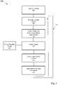
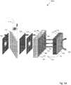
- An additive manufacturing systemwhich has one or more energy sources, including in one embodiment, one or more laser or electron beams, are positioned to emit one or more energy beams.
- Beam shaping opticsmay receive the one or more energy beams from the energy source and form a single beam.
- An energy patterning unitreceives or generates the single beam and transfers a two-dimensional pattern to the beam, and may reject the unused energy not in the pattern.
- An image relayreceives the two-dimensional patterned beam and focuses it as a two-dimensional image to a desired location on a height fixed or movable build platform (e.g. a powder bed). In certain embodiments, some or all of any rejected energy from the energy patterning unit is reused.
- multiple beams from the laser array(s)are combined using a beam homogenizer.
- This combined beamcan be directed at an energy patterning unit that includes either a transmissive or reflective pixel addressable light valve.
- the pixel addressable light valveincludes both a liquid crystal module having a polarizing element and a light projection unit providing a two-dimensional input pattern. The two-dimensional image focused by the image relay can be sequentially directed toward multiple locations on a powder bed to build a 3D structure.
- an additive manufacturing system 100has an energy patterning system 110 with an energy source 112 that can direct one or more continuous or intermittent energy beam(s) toward beam shaping optics 114. After shaping, if necessary, the beam is patterned by an energy patterning unit 116, with generally some energy being directed to a rejected energy handling unit 118. Patterned energy is relayed by image relay 120 toward an article processing unit 140, typically as a two-dimensional image 122 focused near a bed 146. The bed 146 (with optional walls 148) can form a chamber containing material 144 dispensed by material dispenser 142. Patterned energy, directed by the image relay 120, can melt, fuse, sinter, amalgamate, change crystal structure, influence stress patterns, or otherwise chemically or physically modify the dispensed material 144 to form structures with desired properties.
- Energy source 112generates photon (light), electron, ion, or other suitable energy beams or fluxes capable of being directed, shaped, and patterned. Multiple energy sources can be used in combination.
- the energy source 112can include lasers, incandescent light, concentrated solar, other light sources, electron beams, or ion beams.
- Possible laser typesinclude, but are not limited to: Gas Lasers, Chemical Lasers, Dye Lasers, Metal Vapor Lasers, Solid State Lasers (e.g. fiber), Semiconductor (e.g. diode) Lasers, Free electron laser, Gas dynamic laser, "Nickel-like" Samarium laser, Raman laser, or Nuclear pumped laser.
- a Gas Lasercan include lasers such as a Helium-neon laser, Argon laser, Krypton laser, Xenon ion laser, Nitrogen laser, Carbon dioxide laser, Carbon monoxide laser or Excimer laser.
- laserssuch as a Helium-neon laser, Argon laser, Krypton laser, Xenon ion laser, Nitrogen laser, Carbon dioxide laser, Carbon monoxide laser or Excimer laser.
- a Chemical lasercan include lasers such as a Hydrogen fluoride laser, Deuterium fluoride laser, COIL (Chemical oxygen-iodine laser), or Agil (All gas-phase iodine laser).
- laserssuch as a Hydrogen fluoride laser, Deuterium fluoride laser, COIL (Chemical oxygen-iodine laser), or Agil (All gas-phase iodine laser).
- a Metal Vapor Lasercan include lasers such as a Helium-cadmium (HeCd) metal-vapor laser, Helium-mercury (HeHg) metal-vapor laser, Helium-selenium (HeSe) metal-vapor laser, Helium-silver (HeAg) metal-vapor laser, Strontium Vapor Laser, Neon-copper (NeCu) metal-vapor laser, Copper vapor laser, Gold vapor laser, or Manganese (Mn/MnCl 2 ) vapor laser.
- HeCdHelium-cadmium
- HeHgHelium-mercury
- HeSeHelium-selenium
- HeAgHelium-silver
- NeCuNeon-copper
- CuCopper
- AuGold
- Mn/MnCl 2Manganese
- a Solid State Lasercan include lasers such as a Ruby laser, Nd:YAG laser, NdCrYAG laser, Er:YAG laser, Neodymium YLF (Nd:YLF) solid-state laser, Neodymium doped Yttrium orthovanadate(Nd:YVO 4 ) laser, Neodymium doped yttrium calcium oxoborateNd:YCa 4 O(BO 3 ) 3 or simply Nd:YCOB, Neodymium glass(Nd:Glass) laser, Titanium sapphire(Ti:sapphire) laser, Thulium YAG (Tm:YAG) laser, Ytterbium YAG (Yb:YAG) laser, Ytterbium:2O 3 (glass or ceramics) laser, Ytterbium doped glass laser (rod, plate/chip, and fiber), Holmium YAG (Ho:YAG) laser, Chromium ZnSe (Cr:ZnSe) laser
- a Semiconductor Lasercan include laser medium types such as GaN, InGaN, AlGaInP, AlGaAs, InGaAsP, GaInP, InGaAs, InGaAsO, GaInAsSb, lead salt, Vertical cavity surface emitting laser (VCSEL), Quantum cascade laser, Hybrid silicon laser, or combinations thereof.
- laser medium typessuch as GaN, InGaN, AlGaInP, AlGaAs, InGaAsP, GaInP, InGaAs, InGaAsO, GaInAsSb, lead salt, Vertical cavity surface emitting laser (VCSEL), Quantum cascade laser, Hybrid silicon laser, or combinations thereof.
- VCSELVertical cavity surface emitting laser
- Quantum cascade laserHybrid silicon laser
- a single Nd:YAG q-switched lasercan be used in conjunction with multiple semiconductor lasers.
- an electron beamcan be used in conjunction with an ultraviolet semiconductor laser array.
- a two-dimensional array of laserscan be used.
- pre-patterning of an energy beamcan be done by selectively activating and deactivating energy sources.
- Beam shaping unit 114can include a great variety of imaging optics to combine, focus, diverge, reflect, refract, homogenize, adjust intensity, adjust frequency, or otherwise shape and direct one or more energy beams received from the energy source 112 toward the energy patterning unit 116.
- multiple light beamseach having a distinct light wavelength, can be combined using wavelength selective mirrors (e.g. dichroics) or diffractive elements.
- multiple beamscan be homogenized or combined using multifaceted mirrors, microlenses, and refractive or diffractive optical elements.
- Energy patterning unit 116can include static or dynamic energy patterning elements. For example, photon, electron, or ion beams can be blocked by masks with fixed or movable elements. To increase flexibility and ease of image patterning, pixel addressable masking, image generation, or transmission can be used.
- the energy patterning unitincludes addressable light valves, alone or in conjunction with other patterning mechanisms to provide patterning.
- the light valvescan be transmissive, reflective, or use a combination of transmissive and reflective elements. Patterns can be dynamically modified using electrical or optical addressing.
- a transmissive optically addressed light valveacts to rotate polarization of light passing through the valve, with optically addressed pixels forming patterns defined by a light projection source.
- a reflective optically addressed light valveincludes a write beam for modifying polarization of a read beam.
- an electron patterning devicereceives an address pattern from an electrical or photon stimulation source and generates a patterned emission of electrons.
- Rejected energy handling unit 118is used to disperse, redirect, or utilize energy not patterned and passed through the energy pattern image relay 120.
- the rejected energy handling unit 118can include passive or active cooling elements that remove heat from the energy patterning unit 116.
- the rejected energy handling unitcan include a "beam dump" to absorb and convert to heat any beam energy not used in defining the energy pattern.
- rejected beam energycan be recycled using beam shaping optics 114.
- rejected beam energycan be directed to the article processing unit 140 for heating or further patterning.
- rejected beam energycan be directed to additional energy patterning systems or article processing units.
- Image relay 120receives a patterned image (typically two-dimensional) from the energy patterning unit 116 and guides it toward the article processing unit 140.
- the image relay 120can include optics to combine, focus, diverge, reflect, refract, adjust intensity, adjust frequency, or otherwise shape and direct the patterned image.
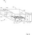
- Article processing unit 140can include a walled chamber 148 and bed 144, and a material dispenser 142 for distributing material.
- the material dispenser 142can distribute, remove, mix, provide gradations or changes in material type or particle size, or adjust layer thickness of material.
- the materialcan include metal, ceramic, glass, polymeric powders, other melt-able material capable of undergoing a thermally induced phase change from solid to liquid and back again, or combinations thereof.
- the materialcan further include composites of melt-able material and non-melt-able material where either or both components can be selectively targeted by the imaging relay system to melt the component that is melt-able, while either leaving along the non-melt-able material or causing it to undergo a vaporizing/destroying/combusting or otherwise destructive process.
- slurries, sprays, coatings, wires, strips, or sheets of materialscan be used. Unwanted material can be removed for disposable or recycling by use of blowers, vacuum systems, sweeping, vibrating, shaking, tipping, or inversion of the bed 146.
- the article processing unit 140can include components for holding and supporting 3D structures, mechanisms for heating or cooling the chamber, auxiliary or supporting optics, and sensors and control mechanisms for monitoring or adjusting material or environmental conditions.
- the article processing unitcan, in whole or in part, support a vacuum or inert gas atmosphere to reduce unwanted chemical interactions as well as to mitigate the risks of fire or explosion (especially with reactive metals).
- Control processor 150can be connected to control any components of additive manufacturing system 100.
- the control processor 150can be connected to variety of sensors, actuators, heating or cooling systems, monitors, and controllers to coordinate operation.
- a wide range of sensorsincluding imagers, light intensity monitors, thermal, pressure, or gas sensors can be used to provide information used in control or monitoring.
- the control processorcan be a single central controller, or alternatively, can include one or more independent control systems.
- the controller processor 150is provided with an interface to allow input of manufacturing instructions. Use of a wide range of sensors allows various feedback control mechanisms that improve quality, manufacturing throughput, and energy efficiency.
- FIG. 1Bis a cartoon illustrating a bed 146 that supports material 144.
- a structure 149is additively manufactured.
- image patterns having non-square boundariescan be used, overlapping or interpenetrating images can be used, and images can be provided by two or more energy patterning systems.
- imagescan be formed in conjunction with directed electron or ion beams, or with printed or selective spray systems.
- FIG. 2is a flow chart illustrating one embodiment of an additive manufacturing process supported by the described optical and mechanical components.
- materialis positioned in a bed, chamber, or other suitable support.
- the materialcan be a powder capable of being melted, fused, sintered, induced to change crystal structure, have stress patterns influenced, or otherwise chemically or physically modified to form structures with desired properties.
- unpatterned energyis emitted by one or more energy emitters, including but not limited to solid state or semiconductor lasers, or electrical power supply flowing electrons down a wire.
- the unpatterned energyis shaped and modified (e.g. intensity modulated or focused).
- this unpatterned energyis patterned, with energy not forming a part of the pattern being handled in step 210 (this can include conversion to waste heat, or recycling as patterned or unpatterned energy).
- the patterned energy, now forming a two-dimensional imageis relayed toward the material.
- the imageis applied to the material, building a portion of a 3D structure.
- stepscan be repeated (loop 218) until the image (or different and subsequent image) has been applied to all necessary regions of a top layer of the material.
- a new layercan be applied (loop 216) to continue building the 3D structure.
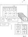
- FIG. 3Ais one embodiment of an additive manufacturing system 300 that uses multiple semiconductor lasers as part of an energy patterning system 310.
- a control processor 350can be connected to variety of sensors, actuators, heating or cooling systems, monitors, and controllers to coordinate operation of multiple lasers 312, light patterning unit 316, and image relay 320, as well as any other component of system 300. These connections are generally indicated by a dotted outline 351 surrounding components of system 300. As will be appreciated, connections can be wired or wireless, continuous or intermittent, and include capability for feedback (for example, thermal heating can be adjusted in response to sensed temperature).
- the multiple lasers 312can emit a beam 301 of light at a 1000 nm wavelength that, for example, is 90 mm wide by 20 mm tall.
- the beam 301is resized by imaging optics 370 to create beam 303.
- Beam 303is 6 mm wide by 6mm tall, and is incident on light homogenization device 372 which blends light together to create blended beam 305.
- Beam 305is then incident on imaging assembly 374 which reshapes the light into beam 307 and is then incident on hot cold mirror 376.
- the mirror 376allows 1000 nm light to pass, but reflects 450nm light.
- a light projector 378capable of projecting low power light at 1080p pixel resolution and 450nm emits beam 309, which is then incident on hot cold mirror 376.
- Beams 307 and 309overlay in beam 311, and both are imaged onto optically addressed light valve 380 in a 20mm wide, 20mm tall image. Images formed from the homogenizer 372 and the projector 378 are recreated and overlaid on light valve 380.
- the optically addressed light valve 380is stimulated by the light (typically ranging from 400-500 nm) and imprints a polarization rotation pattern in transmitted beam 313 which is incident upon polarizer 382.
- the polarizer 382splits the two polarization states, transmitting p-polarization into beam 317 and reflecting s-polarization into beam 315 which is then sent to a beam dump 318 that handles the rejected energy.
- the polarizationcould be reversed, with s-polarization formed into beam 317 and reflecting p-polarization into beam 315.
- Beam 317enters the final imaging assembly 320 which includes optics 384 that resize the patterned light.
- This beamreflects off of a movable mirror 386 to beam 319, which terminates in a focused image applied to material bed 344 in an article processing unit 340.
- the depth of field in the imageselected to span multiple layers, providing optimum focus in the range of a few layers of error or offset.
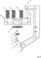
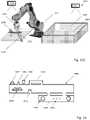
- the bed 390can be raised or lowered (vertically indexed) within chamber walls 388 that contain material 344 dispensed by material dispenser 342. In certain embodiments, the bed 390 can remain fixed, and optics of the final imaging assembly 320 can be vertically raised or lowered. Material distribution is provided by a sweeper mechanism 392 that can evenly spread powder held in hopper 394, being able to provide new layers of material as needed. An image 6 mm wide by 6 mm tall can be sequentially directed by the movable mirror 386 at different positions of the bed.
- the powderWhen using a powdered ceramic or metal material in this additive manufacturing system 300, the powder can be spread in a thin layer, approximately 1-3 particles thick, on top of a base substrate (and subsequent layers) as the part is built.
- a patterned beam 319When the powder is melted, sintered, or fused by a patterned beam 319, it bonds to the underlying layer, creating a solid structure.
- the patterned beam 319can be operated in a pulsed fashion at 40 Hz, moving to the subsequent 6 mm x 6 mm image locations at intervals of 10 ms to 0.5 ms (with 3 to 0.1 ms being desirable) until the selected patterned areas of powder have been melted.
- the bed 390then lowers itself by a thickness corresponding to one layer, and the sweeper mechanism 392 spreads a new layer of powdered material. This process is repeated until the 2D layers have built up the desired 3D structure.
- the article processing unit 340can have a controlled atmosphere. This allows reactive materials to be manufactured in an inert gas, or vacuum environment without the risk of oxidation or chemical reaction, or fire or explosion (if reactive metals are used).
- FIG. 3Billustrates in more detail operation of the light patterning unit 316 of FIG. 3A .
- a representative input pattern 333(here seen as the numeral "9") is defined in an 8x12 pixel array of light projected as beam 309 toward mirror 376.
- Each grey pixelrepresents a light filled pixel, while white pixels are unlit.
- each pixelcan have varying levels of light, including light-free, partial light intensity, or maximal light intensity.
- Unpatterned light 331 that forms beam 307is directed and passes through a hot/cold mirror 376, where it combines with patterned beam 309.
- the patterned light beam 311 formed from overlay of beams 307 and 309 in beam 311, and bothare imaged onto optically addressed light valve 380.
- the optically addressed light valve 380which would rotate the polarization state of unpatterned light 331, is stimulated by the patterned light beam 309, 311 to selectively not rotate the polarization state of polarized light 307, 311 in the pattern of the numeral "9" into beam 313.
- the unrotated light representative of pattern 333 in beam 313is then allowed to pass through polarizer mirror 382 resulting in beam 317 and pattern 335.
- Polarized light in a second rotated stateis rejected by polarizer mirror 382, into beam 315 carrying the negative pixel pattern 337 consisting of a light-free numeral "9".
- Non-optically addressed light valvescan be used. These can include but are not limited to electrically addressable pixel elements, movable mirror or micro-mirror systems, piezo or micro-actuated optical systems, fixed or movable masks, or shields, or any other conventional system able to provide high intensity light patterning.
- electrically addressable pixel elementsmovable mirror or micro-mirror systems, piezo or micro-actuated optical systems, fixed or movable masks, or shields, or any other conventional system able to provide high intensity light patterning.
- these valvesmay selectively emit electrons based on an address location, thus imbuing a pattern on the beam of electrons leaving the valve.
- FIG. 3Cis one embodiment of an additive manufacturing system that includes a switchyard system enabling reuse of patterned two-dimensional energy.
- an additive manufacturing system 220has an energy patterning system with an energy source 112 that directs one or more continuous or intermittent energy beam(s) toward beam shaping optics 114. After shaping, the beam is two-dimensionally patterned by an energy patterning unit 230, with generally some energy being directed to a rejected energy handling unit 222. Patterned energy is relayed by one of multiple image relays 232 toward one or more article processing units 234A, 234B, 234C, or 234D, typically as a two-dimensional image focused near a movable or fixed height bed.
- the bed(with optional walls) can form a chamber containing material dispensed by material dispenser.
- Patterned energydirected by the image relays 232, can melt, fuse, sinter, amalgamate, change crystal structure, influence stress patterns, or otherwise chemically or physically modify the dispensed material to form structures with desired properties.
- the rejected energy handling unithas multiple components to permit reuse of rejected patterned energy.
- Relays 228A, 228B, and 22Ccan respectively transfer energy to an electricity generator 224, a heat/cool thermal management system 225, or an energy dump 226.
- relay 228Ccan direct patterned energy into the image relay 232 for further processing.
- patterned energycan be directed by relay 228C, to relay 228B and 228A for insertion into the energy beam(s) provided by energy source 112.
- Reuse of patterned imagesis also possible using image relay 232. Images can be redirected, inverted, mirrored, sub-patterned, or otherwise transformed for distribution to one or more article processing units. 234A-D.
- reuse of the patterned lightcan improve energy efficiency of the additive manufacturing process, and in some cases improve energy intensity directed at a bed, or reduce manufacture time.
- FIG. 3Dis a cartoon 235 illustrating a simple geometrical transformation of a rejected energy beam for reuse.
- An input pattern 236is directed into an image relay 237 capable of providing a mirror image pixel pattern 238.
- image relay 237capable of providing a mirror image pixel pattern 238.
- more complex pixel transformationsare possible, including geometrical transformations, or pattern remapping of individual pixels and groups of pixels. Instead of being wasted in a beam dump, this remapped pattern can be directed to an article processing unit to improve manufacturing throughput or beam intensity.
- FIG. 3Eis a cartoon 235 illustrating multiple transformations of a rejected energy beam for reuse.
- An input pattern 236is directed into a series of image relays 237B-E capable of providing a pixel pattern 238.
- FIG. 3F and 3Gillustrates a non-light based energy beam system 240 that includes a patterned electron beam 241 capable of producing, for example, a "P" shaped pixel image.
- a high voltage electricity power system 243is connected to an optically addressable patterned cathode unit 245.
- the cathode unit 245is stimulated to emit electrons wherever the patterned image is optically addressed.
- Focusing of the electron beam patternis provided by an image relay system 247 that includes imaging coils 246A and 246B.
- Final positioning of the patterned imageis provided by a deflection coil 248 that is able to move the patterned image to a desired position on a bed of additive manufacturing component 249.
- multiple beams of light from one or more light sourcesare provided.
- the multiple beams of lightmay be reshaped and blended to provide a first beam of light.
- a spatial polarization patternmay be applied on the first beam of light to provide a second beam of light.
- Polarization states of the second beam of lightmay be split to reflect a third beam of light, which may be reshaped into a fourth beam of light.
- the fourth beam of lightmay be introduced as one of the multiple beams of light to result in a fifth beam of light. In effect, this or similar systems can reduce energy costs associated with an additive manufacturing system.
- multiple light beamseach having a distinct light wavelength, can be combined using either wavelength selective mirrors or diffractive elements.
- diffractive elementsIn certain embodiments, reflective optical elements that are not sensitive to wavelength dependent refractive effects can be used to guide a multiwavelength beam.
- Patterned lightcan be directed using movable mirrors, prisms, diffractive optical elements, or solid state optical systems that do not require substantial physical movement.
- a magnification ratio and an image distance associated with an intensity and a pixel size of an incident light on a location of a top surface of a powder bedcan be determined for an additively manufactured, three-dimensional (3D) print job.
- One of a plurality of lens assembliescan be configured to provide the incident light having the magnification ratio, with the lens assemblies both a first set of optical lenses and a second sets of optical lenses, and with the second sets of optical lenses being swappable from the lens assemblies.
- Rotations of one or more sets of mirrors mounted on compensating gantries and a final mirror mounted on a build platform gantrycan be used to direct the incident light from a precursor mirror onto the location of the top surface of the powder bed.
- Translational movements of compensating gantries and the build platform gantryare also able to ensure that distance of the incident light from the precursor mirror to the location of the top surface of the powder bed is substantially equivalent to the image distance. In effect, this enables a quick change in the optical beam delivery size and intensity across locations of a build area for different powdered materials while ensuring high availability of the system.
- a plurality of build chamberseach having a build platform to hold a powder bed, are used in conjunction with multiple optical-mechanical assemblies arranged to receive and direct the one or more incident energy beams into the build chambers.
- Multiple chambersallow for concurrent printing of one or more print jobs inside one or more build chambers.
- a removable chamber sidewallcan simplify removal of printed objects from build chambers, allowing quick exchanges of powdered materials.
- the chambercan also be equipped with an adjustable process temperature controls.
- one or more build chamberscan have a build chamber that is maintained at a fixed height, while optics are vertically movable.
- a distance between final optics of a lens assembly and a top surface of powder bed amay be managed to be essentially constant by indexing final optics upwards, by a distance equivalent to a thickness of a powder layer, while keeping the build platform at a fixed height.
- large and heavy objectscan be more easily manufactured, since precise micron scale movements of the build platform are not needed.
- build chambers intended for metal powders with a volume more than ⁇ 0.1 - 0.2 cubic metersi.e., greater than 100 - 200 liters or heavier than 500 - 1,000 kg will most benefit from keeping the build platform at a fixed height.
- a portion of the layer of the powder bedmay be selectively melted or fused to form one or more temporary walls out of the fused portion of the layer of the powder bed to contain another portion of the layer of the powder bed on the build platform.
- a fluid passagewaycan be formed in the one or more first walls to enable improved thermal management.
- Improved powder handlingcan be another aspect of an improved additive manufacturing system.
- a build platform supporting a powder bedcan be capable of tilting, inverting, and shaking to separate the powder bed substantially from the build platform in a hopper.
- the powdered material forming the powder bedmay be collected in a hopper for reuse in later print jobs.
- the powder collecting processmay be automated, and vacuuming or gas jet systems also used to aid powder dislodgement and removal
- a continuous (long) partcan be sequentially advanced in a longitudinal direction from a first zone to a second zone.
- selected granules of a granular materialcan be amalgamated.
- unamalgamated granules of the granular materialcan be removed.
- the first portion of the continuous partcan be advanced from the second zone to a third zone, while a last portion of the continuous part is formed within the first zone and the first portion is maintained in the same position in the lateral and transverse directions that the first portion occupied within the first zone and the second zone.
- additive manufacture and clean-upe.g., separation and/or reclamation of unused or unamalgamated granular material
- additive manufacture and clean-upmay be performed in parallel (i.e., at the same time) at different locations or zones on a part conveyor, with no need to stop for removal of granular material and/or parts.
- additive manufacturing capabilitycan be improved by use of an enclosure restricting an exchange of gaseous matter between an interior of the enclosure and an exterior of the enclosure.
- An airlockprovides an interface between the interior and the exterior; with the interior having multiple additive manufacturing chambers, including those supporting power bed fusion.
- a gas management systemmaintains gaseous oxygen within the interior at or below a limiting oxygen concentration, increasing flexibility in types of powder and processing that can be used in the system.
- capabilitycan be improved by having a 3D printer contained within an enclosure, the printer able to create a part having a weight greater than or equal to 2,000 kilograms.
- a gas management systemmay maintain gaseous oxygen within the enclosure at concentrations below the atmospheric level.
- a wheeled vehiclemay transport the part from inside the enclosure, through an airlock, since the airlock operates to buffer between a gaseous environment within the enclosure and a gaseous environment outside the enclosure, and to a location exterior to both the enclosure and the airlock.
- Other manufacturing embodimentsinvolve collecting powder samples in real-time in a powder bed fusion additive manufacturing system.
- An ingester systemis used for in-process collection and characterizations of powder samples. The collection may be performed periodically and the results of characterizations result in adjustments to the powder bed fusion process.
- the ingester systemcan optionally be used for one or more of audit, process adjustments or actions such as modifying printer parameters or verifying proper use of licensed powder materials.
- a manipulator devicesuch as a crane, lifting gantry, robot arm, or similar that allows for the manipulation of parts that would be difficult or impossible for a human to move is described.
- the manipulator devicecan grasp various permanent or temporary additively manufactured manipulation points on a part to enable repositioning or maneuvering of the part.
- FIG. 4Aillustrates a beam combining system 400 having multiple wavelength semiconductor lasers and using transmissive imaging optics.
- the discussed laser powers and wavelengthsare exemplary, as are the selected wavelengths reflected or transmitted by wavelength filters. With the appropriate changes in positioning and use of wavelength filters, greater or lesser numbers of lasers can be used.
- solid state laserscan be substituted or used in combination with semiconductor lasers.
- other laser typessuch as discussed with respect to FIG. 1 , including gas, chemical, or metal vapor lasers can be used.
- recycling and reuse of rejected lightcan substitute for a laser. Rejected light available in an additive manufacturing system can be collected, homogenized and re-introduced into a beam line.
- recycling and re-using rejected lightcan increase beam intensity and reduce energy costs associated with the system.
- semiconductor lasers of a first wavelength (1020nm) 406emit a 33.3kW beam of photons of a corresponding wavelength 407
- semiconductor lasers of a second wavelength (1000nm) 408emit a 33.3kW beam of photons of the corresponding wavelength 409, which are then combined using a wavelength filter 410 that transmits 1020nm photons, but reflects 1000nm photons. This results in a combined two-wavelength beam 411 of 66.6kW.
- Semiconductor lasers of a third wavelength (980nm) 412emit a 33.3kW beam of photons of the corresponding wavelength 413 which are then combined with beam 411 using a wavelength filter 414.
- Wavelength filter 414transmits 1020 and 1000nm, but reflects the 980nm beam, resulting in a three-wavelength beam 415 of 99.9kW.
- Semiconductor lasers of a fourth wavelength (960nm) 417emit a 33.3kW beam of photons of the corresponding wavelength 418 which are then combined with beam 415 using a wavelength filter 416 that transmits 1020nm, 1000nm, and 980nm photons, but reflects 960nm, resulting in a four-wavelength beam 419 of 133.2kW.
- This beamenters the optical imaging system with beam dimensions, for example, of 20mm x 20mm and a divergence of 1.1 degrees at lenses 420.
- Lenses 420are a series of lenses that use two materials, C79-79 and ULE 7972, each having a different index of refraction, to cancel out the effect of wavelength variance on the ability to image the beam.
- the beamexits the optical system at 421, which is a series of lenses that utilizes three materials, ZeruDur, ULE 7972, and C79-79 to cancel out the effect of wavelength variance on the ability to image the beam.
- the beam at 422has been increased in intensity as a result of passing through the optical system and is now 6mm wide x 6mm tall at 3.67 degrees of divergence resulting in an intensity of 370kW/cm 2 , sufficient for the additive manufacturing processing of metals such as powdered stainless steel.
- Transmissive opticssuch as lenses 420 can be made with fused silica glass. This reduces thermal expansion problems due to extremely low coefficients of absorption at wavelengths near 1000nm, and reduces thermal expansion of lenses due to the extremely low coefficients of thermal expansion fused silica.
- fused silicaallows for the optics to withstand much higher intensities without heating up and expanding which can lead to fracture, changes in the glass index of refraction, changes in glass shape, and consequent changes in focal points.
- Unwanted optical changescan also be reduced by use of two or more materials. Each material can have a different index of refraction which changes differently with wavelength. Used in the appropriate combination, the changes in index and optical path length cancel out, and there no variance in focal distance as a function of wavelength.
- FIG. 4Billustrates an alternative beam combining system 401 that includes a combination of multiple wavelength semiconductor lasers and uses reflective imaging optics to reduce the foregoing discussed issues associated with transmissive optics.
- the discussed laser powers and wavelengths in system 401are exemplary, as are the selected wavelengths reflected or transmitted by wavelength filters. With the appropriate changes in positioning and use of wavelength filters, greater or lesser numbers of lasers can be used. Multiple types of lasers can be used, and in one embodiment, recycling and reuse of rejected light can substitute for a laser. Rejected light available in an additive manufacturing system can be collected, homogenized and re-introduced into a beam line.
- reflective opticsimprove problems associated with semiconductor laser chirp (shift of wavelength over time) during startup transients and over their lifetime.
- the use of reflective opticsprevents detuning of diode laser focus due to this effect and does not affect the resolution achieved or imaging capability.
- wavelength differences caused by variation in laser operating temperaturedo not affect the resolution or imaging capability.
- semiconductor lasers of a first wavelength (1020nm) 423emit a 33.3kW beam of photons of the corresponding wavelength 424
- semiconductor lasers of a second wavelength (1000nm) 425emit a 33.3kW beam of photons of the corresponding wavelength 426.
- These beamsare combined using a wavelength filter 427 that transmits 1020nm photons, but reflects 1000nm photons, resulting is a two-wavelength beam 428 of 66.6kW.
- Semiconductor lasers of a third wavelength (980nm) 429emit a 33.3kW beam of photons of the corresponding wavelength 430.
- beamsare combined with beam 428 using a wavelength filter 431 which transmits 1020 and 1000nm, but reflects 980nm, resulting in a three-wavelength beam 432 of 99.9kW.
- Semiconductor lasers of a fourth wavelength (960nm) 433emit a 33.3kW beam of photons of the corresponding wavelength 434.
- These beamsare combined with beam 432 using a wavelength filter 435 that transmits 1020nm, 1000nm, and 980nm photons, but reflects 960nm, resulting in a four-wavelength beam 436 of 133.2kW.
- This beamenters the optical imaging system with, for example, beam dimensions of 20mm x 20mm and a divergence of 1.1 degrees at reflective optic 437.
- Reflective opticshave no dependence on wavelength and do not affect the ability to image the beam.
- the beamexits the beam combining optical system 401 at reflective optic 438.
- the beam 439has been increased in intensity as a result of passing through the optical system and is now 6mm wide x 6mm tall at 3.67 degrees of divergence resulting in an intensity of 370kW/cm 2 , sufficient for the additive manufacturing processing of metals such as powdered stainless steel.
- FIG. 4Cillustrates an alternative embodiment of a beam combining system 440 that combines beams 443 from same or multiple wavelength lasers 442 using a diffractive imaging optic 444.
- the diffractive opticcan be shaped or patterned to receive beams 443, and reflect them along a substantially same beam axis.
- a diffractive optic that reflects beamsis shown in FIG. 4C , in other embodiments the diffractive optic can transmit beams, or use a combination of reflective, transmissive , or other suitable beam steering optical assemblies or components.
- FIG. 5Ais a reflective optically addressed light valve system 500A useful in additive manufacturing systems such as disclosed herein.
- Reflective light valvesdo not need to transmit light through a transparent semiconductor for light patterning, where at high average power levels, even small amounts of absorption can cause unwanted and catastrophic heating. Reflective light valves can also allow for a greater ease of cooling on the reflective surface, with cooling on an opposing side to where the write beam and the read beam are incident.
- the reflective optically addressed light valve system 500Ais capable of patterning an energy beam and is composed of a highly transmissive layer 501, a twisted nematic (TN) liquid crystal layer 502, and a photoconductor layer 503.
- the highly transmissive layeris optically transparent for 1000nm and 700nm light, made from glass substrate (C79-79 fused silica) 501 which has anti-reflective coatings on both sides at 504 and 506.
- An Indium Tin Oxide (ITO) conductive coatingis applied to highly transmissive layer 501 at 505.
- Layer 502is anchored to 506 and 510 by way of anchoring substrates 507 and 509.
- the exact spacing of 502is given by the size of the spacer balls 508 which define a gap of 2.5 microns, tuned for maximum contrast ratio when passing 1000nm light in a double pass.
- Layer 503is made of a single crystalline silicon semiconductor with a high reflection dielectric coating applied at 510 which is transparent to 700nm, but reflective at 1000nm.
- Layer 511is another layer of ITO which has a solder point attached 512 and is connected to layer 505 by way of an AC voltage source 514 by way of another solder point 513.
- a patterned write beam of lightis emitted from a projector source at 700nm and is incident on 503 after transmitting through 504, 501, 505, 506, 507, 502, 509 and 510.
- the "read" beam 516is p-polarized and is incident on 510 after transmitting through 504, 501, 505, 506, 507, 502, and 509 at which point it reflects and transmits back through 509, 502, 507, 506, 505, 501, and 504 to exit the light valve system 500A.
- This beamis then incident on a polarizer 517 which reflects s-polarization resulting in reflected beam 518 and transmits p-polarization resulting in transmitted beam 519. Even though absorption is very low in the device the HR coating 509 is not perfectly reflecting and some energy is absorbed. This energy is removed by radiative, conductive, or convective cooling 520.
- FIG. 5Billustrates an alternative reflective optically addressed light valve 500B with cooling on one side where the write beam and the read beam are incident from the different sides.
- the valveis composed of a highly transmissive layer 521, a twisted nematic (TN) liquid crystal layer 522, and a photoconductor layer 523.
- the highly transmissive layeris optically transparent for 1000nm and 700nm light, made from glass substrate (C79-79 fused silica) 521 which has anti-reflective coatings on both sides at 524 and 526.
- An Indium Tin Oxide (ITO) conductive coatingis applied to 521 at 525.
- Layer 522is anchored to 526 and 530 by way of anchoring substrates 527 and 259.
- ITOIndium Tin Oxide
- Layer 523is made of a single crystalline silicon semiconductor with a high reflection dielectric coating applied at 530 which reflective at 1000nm.
- Layer 531is another layer of ITO which has a solder point attached 532 and is connected to layer 525 by way of an AC voltage source 534 by way of another solder point 533.
- a patterned write beam of lightis emitted from a projector source at 700nm and is incident on 523 after transmitting through a an optional convective/conductive substrate 540 and through the ITO coating 531.
- the "read" beam 536is p-polarized and is incident on 530 after transmitting through 524, 521, 525, 526, 527, 522, and 529 at which point it reflects and transmits back through 529, 522, 527, 526, 525, 521, and 524 to exit the light valve.
- This beamis then incident on a polarizer 537 which reflects s-polarization resulting in reflected beam 538 and transmits p-polarization resulting in transmitted beam 539. Even though absorption is very low in the device the HR coating 529 is not perfectly reflecting and some energy is absorbed. This energy is removed by radiative, conductive, or convective cooling 540.
- Apparatus 600may include one or more light sources such as, for example and without limitation, light sources 601, 602, and 603.
- light sources 601, 602, and 603may include lasers.
- other types of light sourcessuch as solid state lasers may be utilized.
- each or at least one of light sources 601, 602, and 603may emit 11.1kW of p-polarized light at 700nm, having a size of 7.9cm x 7.9cm, and 7.6mrad in divergence.
- Beams of light emitted by light sources 601, 602, and 603may be multiplexed together by a first optical assembly 604, which may include a series of mirrors, thus allowing the beams to be as close together as possible. These beams are then reshaped and blended by an optical device 605, resulting in a beam 6, 33.3kW, 4.7cm x 4.7cm and 70.4mrad in divergence. Beam 606 may then be incident on a spatial polarization valve 607, which can apply a spatial polarization pattern map on beam 606 by rotating the polarization of selected pixels from p-polarization to s-polarization to provide a beam 8.
- the selected pixelscan be formed by rotating from s-polarization to p-polarization to provide the beam.
- grey scale pixelscan be created by partial rotations.
- the s-polarization state of beam 608may be reflected into a beam 610.
- the exact fractionmay be given as a function of the fraction of light that is patterned by a spatial polarization valve 607.
- Beam 10may enter a second optical assembly 611, which may include a series of mirrors, re-shaping lenses, waveplates, or other optical components, and may be modified into a 7.9cm x 7.9cm beam and then re-introduced to the system as if it were a light source 612, along with the original one or more light sources 601, 602, and 603.
- a second optical assembly 611which may include a series of mirrors, re-shaping lenses, waveplates, or other optical components, and may be modified into a 7.9cm x 7.9cm beam and then re-introduced to the system as if it were a light source 612, along with the original one or more light sources 601, 602, and 603.
- a process for light recyclingcan include the steps of multiplexing multiple beams of light including at least one or more beams of light from one or more light sources 601, 602, and 603.
- the multiple beams of lightcan be reshaped and blended to provide a first beam of light.
- a spatial polarization valve 607 of apparatus 600applies a spatial polarization pattern on the first beam of light to provide a second beam of light.
- a polarizer 609 of apparatus 600splits polarization states of the second beam of light 608 to reflect a third beam of light (e.g., beam 610).
- a second optical assembly 611 of apparatus 600reshapes the third beam of light into a fourth beam of light, and the fourth beam of light is introduced to first optical assembly 604 as one of the multiple beams of light to result in a fifth beam of light (e.g., beam 613) that is emitted through and not reflected by polarizer 609.
- a fifth beam of lighte.g., beam 613
- FIG. 7illustrates an example optical assembly 700 of polarization combining to achieve up to 2x of the original semiconductor laser intensity (in the limit).
- Semiconductor lasersare typically polarized to about 70-90% in one polarization state.
- polarization rotating methodto pattern the light, the 10-20% of the light in the undesired polarization state could potentially go unused (rejected).
- polarization combining and patterningcan be used to either boost transmission efficiency or increase resultant intensity by a factor of 2, or both.
- two or more beams of light with a first intensityare provided, each of the two or more beams of light being polarized and having a majority polarization state and a minority polarization state.
- a respective polarization patternis applied on the majority polarization state of each of the two or more beams of light and the two or more beams of light are combined to provide a single beam of light with a second intensity greater than the first intensity.
- more than one laser of an arbitrary polarization statecan be used.
- a polarizeris used to split the beam(s) into its (their) respective polarization state(s), and spatially stack the beam(s) of corresponding polarization state(s) close together by spatial positioning creating two effective beams, with one of each polarization state. These two beams, of different polarization state, are then passed through a light modulator relating to their perspective polarization state, then with a polarization state pattern applied in the beam, and subsequently beam combined by polarization combining.
- This methoduses all light in the process, which allows for higher usage of the laser light, thereby achieving minimal to no losses, due to variance in polarization state, as well as better system efficiency.
- Optical assembly 700may include some or all of those components shown in FIG. 7 , to be described as follows.
- Light sources 701 and 702are each used as a high power photon source.
- light sources 701 and 702may be semiconductor laser arrays with 33.3kW of power each, emitting photons at 1000nm that are shaped and blended into a square beam 20mm wide x 20mm.
- Emitted lightmay be 90% polarized in a majority state p resulting in light beams 703 and 704.
- the emitted light beams 703 and 704may be incident on polarizers 705 and 706, respectively.
- Polarizers 705 and 706may reflect minority state s-polarization to result in light beams 709 and 7010, which may be incident on a beam dump 7011. Polarizers 705 and 706 may transmit p-polarization to result in light beams 706 and 707, which may be incident on polarization rotating optically addressed light valves 712 and 13, respectively. Each of light valves 712 and 713 may have the same image applied to light beams 706 and 707 to create polarization patterns, and may spatially flip 20% of the "pixels" from p-polarization to s-polarization in the desired patterns resulting in light beams 714 and 715. Beams 714 and 715 may be incident on polarizers 716 and 717, respectively.
- Polarizers 716 and 717may reflect s-polarization to result in light beams 718 and 719, respectively, which may contain 20% of the energy and may be dumped to a beam dump 720.
- Polarizers 716 and 717may transmit p-polarization to result in light beams 721 and 722.
- Beam 722may be incident on a half wave plate 723 which rotates the polarization of every photon by a half wave, thereby turning p-polarization to s-polarization to result in light beam 724.
- Beams 721 and 724may be incident on mirrors 725 and 726, respectively, to result in light beams 727 and 728.
- Beam 727may be incident on mirror 729 to result in beam 730, which may be incident on polarizer 731 in p-polarization.
- Beam 728 in s-polarizationmay be incident on polarizer 731 which may reflect s-polarization of beam 728 and transmit p-polarization of beam 730 to result in light beam 732.
- Beam 732may be a beam of twice the intensity of a single polarization state from light source 701 or 702, for a total initial intensity of 1.8x the original due to the 90% initial polarization, and proportionally less that for the 20% of the polarization map image applied at light valves 712 and 713.
- Total propagated intensity at beam 732may be 1.44x the initial intensity for a total transmitted power of 47.52kW emitted. Imaged to the original 20x20mm square, the final intensity may be 11.88kW/cm2 if divergence angle is maintained.
- a source image of an optical beam of sufficient energyis directed to locations on the top surface of a powder bed (print surface) to form an integral object when a powdered material is processed (with or without chemical bonding).
- the resolution (or a pixel size) of an optical system used for powder bed fusion additive manufacturingdepends on whether the print surface coincides with the focal plane of the final optics in the optical system, or in term for imaging systems, depending on whether the distance between lenses and image planes for optics performing an imaging operation stays substantially a constant distance for a given lens configuration.
- FIG. 8is a flow chart 800 illustrating steps for use of a dynamic optical assembly that can include an image relay gantry.
- step 810information is obtained or otherwise determined to find a minimum resolution (a pixel size of an incident light) for an object to be printed in the powder bed fusion additive manufacturing system.
- a magnification ratio of the incident light containing an image information and an image distance of dynamic optical assemblyis calculated.
- the magnification ratiomay transfer a first size of the image at a precursor image plane to a second size of the image at the print surface (top surface of a powder bed).
- the incident lightmay be originated from energy source and passes through the precursor image plane at which the image information may be created.
- Process 800may involve storing geometrical data of the object, positional and rotational control data of the dynamic optical assembly.
- process 800can include configuring a mechanical assembly and one or more of lens assemblies to achieve the magnification ratio obtained at 810 suitable for the powdered material.
- the configuring of mechanical assembly and one of lens assembliesmay involve a rotation of mechanical assembly, a swap of second sets of optical lenses, or a removal of a second set of optical lenses.
- a plurality of rotationscan be performed to direct the incident light from the precursor image plane to the print surface at a desired location on the print surface (e.g., top surface of a powder bed) in each successive step of powder bed fusion additive manufacturing.
- the dynamic optical assemblycan perform a plurality of translational movements to maintain a constant image distance from the precursor image plane to every location of the print surface (e.g., top surface of a powder bed) in each successive step of powder bed fusion additive manufacturing.
- Vertical motion of the powder bed or the optical assemblycan be used to maintain a fixed separation of the powder bed with respect to a final lens.
- An apparatus to implement process 800can include a layer of a powdered material dispensed on a top surface of a powder bed supported by a build platform.
- Source image of an incident light located at a precursor image planeis incident upon lens assembly in barrel.
- Lens assemblymay be configured by a rotation of barrel that effect a swap of a second set of optical lenses, a removal of a second set of optical lenses, use of dynamic lenses that change shape, electronic lens swapping, beam redirect systems, electro-optically controlled refractive beam steering devices, or a combination thereof, to have a suitable magnification ratio for the powdered material.
- Object image of a size different than source imageappears after passing through lens assembly, and is modified according to the magnification ratio of lens assembly.
- the beam containing image information ofis incident on precursor mirror and is directed to mirror mounted on compensating gantry where it reflects off mirror and then is incident on final mirror mounted on build platform gantry.
- Final mirrordirects the beam containing image information through a final lens toward a top surface of a powder bed and object image is recreated and magnified in image plane which may be formed thereon.
- the powdered material on powder bedmay melt to form a shape of object image.
- Build platform gantrythen moves to a next location until designated locations on the top surface of powder bed are bonded for that layer.
- a new layer of the powdered materialis dispensed again and the build platform may move down a distance equal to the thickness of the layer of the powdered material to keep a constant distance to the build platform gantry.
- the cyclestarts for the new layer in continuing the additive printing process.
- FIG. 9Aillustrates an example scenario 900 of an intermediate point in a powder bed fusion additive manufacturing printing process.
- Example scenario 800shows upward movements of components in the build chamber while controlling the depth of field with a stationary build platform 930.
- Build platform 930may have an area of 0.5 meter by 1 meter on which powders may be dispensed during a print cycle.
- build platform 930is moved into position beneath gantry table 905 and locked into position.
- a powder dispensing unit 910, a compacting functionality 911, and a mirror 917may be mounted on gantry 907 for translational movements in a horizontal plane.
- Gantry table 905is shown at a position higher above powder bed 920 in FIG. 8 to reflect that printing may be in progress.
- Powder bed 920contains both powder layers and printed object(s) in various stages of completion.
- a new layer of powders 925is dispensed from powder dispensing unit 910 that includes powder spreading and compacting. Beam 921 incident from print head (not shown) may be reflected off a mirror 917 to become beam 922 impinging upon a location 923 in the new layer of powders 925. Printing can occur by melting, sintering, fusing, or otherwise amalgamating of powders at location 923 in the new layer of powders 925.
- the distance between mirror 917 and the location 923 in the new layer of powders 925is the depth of field that needs to be tightly controlled to satisfy a resolution requirement.
- An arrow 970indicates an upward movement of gantry table 905, which supports gantry 907, powder dispensing unit 910, mirror 917, and in certain embodiments, a surrounding chamber or wall. During this process, the build platform 930 remains locked into place, and the gantry 907 (and/or chamber and chamber wall) moves relative the build platform 930. This arrangement is particularly useful for embodiments discussed below, in which the build platform 930 is large, and will need to support a large amount of heavy material that is not easily moved in a vertical direction with required precision.
- build platform 930 of example scenario 900may have an area of more than 0.25 square meters. Alternatively, build platform 930 of example scenario 900 may have an area of more than 0.5 square meters. Alternatively, build platform 930 of example scenario 900 may have an area of more than 1 square meters. Alternatively, build platform 930 of example scenario 900 may have an area of more than 5 square meters. Alternatively, build platform 930 of example scenario 900 may have an area of more than 10 square meters. Alternatively, build platform 930 of example scenario 900 may have an area of more than 50 square meters.
- powder bed 920 including the printed object of example scenario 900may have a mass of more than 10 kilograms.
- powder bed 920 including the printed object of example scenario 900may have a mass of more than 50 kilograms.
- powder bed 920 including the printed object of example scenario 900may have a mass of more than 100 kilograms.
- powder bed 920 including the printed object of example scenario 900may have a mass of more than 500 kilograms.
- powder bed 920 including the printed object of example scenario 900may have a mass of more than 1,000 kilograms.
- powder bed 920 including the printed object of example scenario 900may have a mass of more than 2,000 kilograms.
- powder bed 920 including the printed object of example scenario 900may have a mass of more than 5,000 kilograms.
- powder bed 920 including the printed object of example scenario 900may have a mass of more than 10,000 kilograms.
- build platform 930 of example scenario 900may have an area of more than 0.25 square meters and powder bed 920 including the printed object of example scenario 900 may have a mass of more than 10 kilograms.
- Powder bed fusion techniqueprocess powdered materials to form integral objects out of metal, ceramic, and plastic powders. Sufficient energies are needed to bring powders to the respective melting/sintering/alloying temperatures, or phase transition temperatures. If a powdered material starts out closer to its phase transition temperature, less energy may be required to complete the phase transition.
- the powder bed fusion additive manufacturingmay benefit from pre-heating of the powder bed to reduce the amount of energy delivered by the lasers or other energy sources. This may allow using a lower intensity laser and less dwell time to bond a powder, increasing the throughput rate.
- Post processing heat treatmentsmay be required for some powdered materials such as metals to mitigate stress concentrations and increase mechanical strengths.
- Post processing heat treatmentsmay include a controlled-temperature anneal or a fast cooling to improve desired mechanical or electrical properties.
- Pre-heating of powders and post processing heat treatmentsmay be achieved by embedding heating/cooling element(s)/temperature sensor(s) inside walls of a build chamber/inside a build platform and controlling the rate of heating/cooling with a feedback algorithm. Heat loss may be reduced by using insulating materials inside walls of a build chamber.
- FIG. 9Billustrates an example apparatus of laser-based powder bed fusion additive manufacturing system 900B in accordance with an embodiment of the present invention.
- the system 900Bincludes both an energy source 950 and energy beam steering systems/drivers 955 as part of a printhead 910B.
- An optical-mechanical assembly 930(1)-930(N)can distribute energy beams for the printhead 910B through the system 900B.
- Data input, monitoring, control, and feedback control using various sensorsis enabled by processor(s) 901 and memory 940. These systems can include input of 3D object data 941, print head control 942, build platform control 943, optical-mechanical assembly control 944, and build chamber control 945
- Laser-based powder bed fusion additive manufacturing system 900includes according to the present invention a plurality of build chambers. illustrative purpose and without limitation, one or more build chambers of system 900 are shown in FIG. 9B as build chambers 920B(N), with N being a positive integer greater than or equal to 1.
- Build chambers 920B(1) - 920B(N)may include powder dispensing units 922(1) - 922(N) for dispensing powdered materials and build platforms 924(1) - 924(N) to support powder beds formed by powdered materials.
- Each of build chambers 920B(1) - 920B(N)may have a different size and may be swappable among each other within powder bed fusion additive manufacturing system 900.
- Build chambers 920B(1) - 920B(N)may have removable doors to facilitate powder removal from a side of build chambers 920B(1) - 920B(N) after a build.
- Build chambers 920B(1) - 920B(N)may be sealed in an atmosphere during powder bed fusion additive manufacturing.
- the atmospheremay include, but not limited to, vacuum, air, nitrogen, argon, or helium.
- walls/ceilings of build chambers 920B(1) - 920B(N)may be embedded with heating/cooling elements 926(1) - 926(N) and temperature sensors 928(1) - 928(N) to control the thermal environment inside build chambers 920B(1) - 920B(N).
- heating/cooling elements 926(1) - 926(N)may be fluid channels capable of heat exchange.
- the fluidmay be heated or cooled outside build chambers 920B(1) - 920B(N) and perform heat exchange with the walls/ceilings by moving fluid through the fluid channels.
- the fluidmay include, but not limited to, an oil, water, steam, air, nitrogen, argon, or a coolant.
- heating/cooling elements 926(1) - 926(N)may be resistive heating elements and thermionic cooling elements respectively.
- temperature sensors 928(1) - 928(N)may be thermocouples embedded inside walls/ceilings of inside build chambers 920(1) - 920(N).
- temperature sensors 928(1) - 928(N)may be infrared camera(s) mounted on walls/ceilings inside build chambers 920(1) - 920(N).
- each of build chambers 920(1) - 920(N)includes radiation shields on walls/ceilings of build chambers 920(1) - 920(N) to reduce heat loss.
- build chambers 920(1) - 920(N)may include low thermal conductance materials as parts of walls/ceilings.
- each of build platforms 924(1) - 924(N)may be capable of vertical motions or being fixed at a given height during powder bed fusion additive manufacturing.
- Build platforms 924(1) - 924(N)may have different sizes and support variable masses of powder beds.
- Build platforms 924(1) - 924(N)may be removable from build chambers 920(1) - 920(N) on rails, wheels or other means.
- FIG. 10describes a method to minimize powder volume requirements during a build operation.
- Process 1000may be utilized to realize printing variable print chamber walls for powder bed fusion in a powder bed fusion additive manufacturing system.
- process 1000may involve dispensing a powdered material to form a first layer of a powder bed on a support surface of a build platform.
- process 1000may involve selectively fusing a portion of the first layer of the powder bed to form one or more first walls out of the fused portion of the first layer of the powder bed.
- the one or more first wallsmay contain another portion of the first layer of the powder bed on the build platform.
- the one or more first wallsmay include multiple walls surrounding an area interior of the build platform to create a region devoid of the powdered material.
- process 1000may involve dispensing the powdered material to form a second layer of the powder bed on the first layer of the powder bed.
- process 1000may involve selectively fusing a portion of the second layer of the powder bed to form one or more second walls out of the fused portion of the second layer of the powder bed.
- the one or more second wallsmay contain another portion of the second layer of the powder bed.
- the one or more first wallsmay include multiple first walls surrounding another portion of the first layer of the powder bed over a first area of the build platform.
- the one or more second wallsmay include multiple second walls surrounding another portion of the second layer of the powder bed over a second area of the first layer of the powder bed, with the second area being smaller than the first area.
- the one or more first wallsmay include at least one wall along at least one perimeter of multiple perimeters of the build platform. Additionally, the remaining one or more perimeters of the multiple perimeters of the build platform may border one or more structural walls.
- process 1000may further involve causing a relative movement between the build platform and the one or more structural walls in a direction perpendicular to the support surface of the build platform. Moreover, process 1000 may involve dispensing the powdered material on the first layer of the powder bed and the one or more first walls to form a second layer of the powder bed. Furthermore, process 1000 may involve selectively fusing a portion of the second layer of the powder bed to increase a height of the one or more first walls.
- temporary wallscan be produced to have pipes, cavities, or porous sections (hereinafter "fluid passageways") able to support fluid flow.
- the fluid passagewayscan be open, or partially closed, and can be formed to interface with external pipes, hoses, sprayers, or other fluid communication systems. Air, nitrogen, water, high temperature or silicone oils, or other suitable gas or liquid can be circulated or otherwise transferred through a fluid passageway to improve thermal management.
- Thermal managementcan include both fast or controlled cooling, and the fluid can be circulated (e.g. through pipes formed in the temporary walls) or sprayed, dripped, or splashed against, for example, a porous outer wall section.
- the proposed schememay be implemented in powder bed fusion additive manufacturing systems for printing metal, plastic, or ceramic parts. Applications of the proposed scheme may be more specifically defined as for use in the print bed part of the machine on the receiving end of the laser or electron beam.
- one or more energy sources of a print head of a powder bed fusion additive manufacturing systemmay be controlled to print walls of a build chamber. This allows for elimination of the edge walls of the chamber, and can allow for sub-set areas to be created. The presence of sub-set areas/volumes/voids can help minimize powder usage, and enables the creation of volumes devoid of powder.
- powdermay be selectively distributed across the build area in pre-defined walled areas created during the additive manufacturing process.
- print chamber wallsto support previously deposited layers consisting of powder and printed object(s).
- One examplemay involve raising to a close-fitting wall.
- Another examplemay involve printing a perimeter wall (and perhaps structural support for it) during each layer. This wall may be cut out and recycled after each print.
- most or all of the surrounding wallsmay be raised, and a wall may be also printed to lessen the powder bed area for the layer of powder while using a "tub" formed by the surrounding walls for catchment of powder falling outside the printed wall.
- the raised wallmay be not intended as a full perimeter. For instance, access points for a fork lift or other material handling equipment may be needed when the print bed is first put into the print station and later when the completed bed (powder and printed object(s)) are lifted out. The printing of a limited wall for this area provides the required remaining wall to support the powder during a print cycle. The material handling equipment potentially can then "punch" through this printed wall to gain access to the lift points.
- the lift pointsmay be determined by an algorithm or user placement a priori the build and are built into the walls in key locations.
- the printed walldoes not need to match geometry of the print table, nor exactly match a wall printed in a previous layer. This allows, with the appropriate powder dispensing equipment and logic, powder to be dispersed just enough to cover between the walled areas where powder is needed. Advantageously, this can save a tremendous amount of time, weight and/or powder per layer.
- Fig. 11Aillustrates an example scenario 1100 in which a powder bed 1120 is formed on a build platform 1130.
- the build platform 1130may have an area of 0.25 square meter and may support a powder bed 1120 of a powdered material, which may be 0.5 m deep inside a build chamber 1110. Scenario 1100 may be at the end, or in the middle of a print cycle.
- a hopper 1140with sloped walls which may be 45- 60 degrees relative to a horizontal surface on which build platform 1130 is disposed.
- hopper 1140may contain an auger 1150.
- FIG. 11Billustrates another example scenario 1101 in which the separation of a powder bed 1121 from a build platform 1131 is depicted.
- Scenario 1101may be at the end of a print cycle or in a mid-cycle that is aborted due to various reasons.
- a build platform 1131 supporting the powder bed 1121may be tilted over 90 degrees from a horizontal position.
- the gravity pull due to the weight of the powder bed 1121causes the powdered material and the printed object(s) embedded within the powder bed 1121 to fall in a hopper 1141 below.
- the build chamber 1111may include a vacuum 1160 and a high pressure jet 1162 so that a substantial portion of powders may be collected in the hopper 1141.
- the vacuuming 1160 and gas-jetting 1162may be utilized to dislodge sticky powders remained on the build platform 1131 after tilting the build platform 1131.
- the hopper 1141may have sloped walls to help guide powders onto the bottom of the hopper 1141.
- the hopper 1141may include an auger 1151.
- Processingcan involve controlling a powder dispensing assembly to dispense a plurality of layers of a powdered material in forming a powder bed during a print cycle.
- Vertical motion of powder dispensing assemblycan be controlled to maintain a constant separation from the powder bed.
- the vertical motionresults in indexing powder dispensing assembly can be away from the powder bed (e.g., upwards) by a distance equivalent to a thickness of a dispensed powder layer after a portion of dispensed powder layer is bonded together.
- movement of the build platformmay include rotating, tilting, inverting, vibrating, shaking and/or jittering. As a result of these motions, the powder bed on build platform may fall into hopper below build platform due to weight of the powder bed.
- Vacuum systems, mechanical arm, and/or gas sprayercan be used to further dislodge remaining powders on build platform.
- a substantial portion of the powdered materialmay be collected in hopper for reuse or for storage.
- an auger and/or conveyercan be used to transport collected powders in hopper towards one or more of storage chambers.
- a substantial portion of the powdered materialcan be sealed in one or more of storage chambers an atmosphere suitable for the powdered material.
- the atmospheremay include vacuum, air, nitrogen, argon, helium, other inert gas, or noble gas.
- FIGS.12A and 12Billustrates a system for long part manufacture.
- Many current 3D printershave significant and recurrent downtime when a build chamber must be emptied of powder and printed parts and reset for the next print job.
- a uniform coordinate system 1211is defined. Accordingly, certain systems may correspond to or define longitudinal, lateral, and transverse directions 1211a, 1211b, 1211c that are orthogonal to one another.
- the longitudinal direction 1211amay correspond to a long axis of a system. Accordingly, during additive manufacture, a long axis of a long part 1210 may be substantially aligned with the longitudinal direction 1211a.
- the lateral direction 1211bmay combine with the longitudinal direction 1211a to define a horizontal plane. That is, the longitudinal and lateral directions may both extend within a horizontal plane.
- the transverse direction 1211bmay extend up and down in alignment with gravity.
- systems and methodsmay enable or support substantially continuous additive manufacture that does not have such downtime. As can be seen with reference to FIGS. 12A and 12B , this may be accomplished by manufacturing a part 1210 in segments. For example, a system can (1) manufacture a first segment 1212a of a part 1210, (2) advance the part 1210 a selected distance down a conveyor 1216, (3) manufacture a second segment 1212b of the part 1210, (4) advance the part 1210 a selected distance down the conveyor 1218, and (5) repeat until all segments of the part 1210 have been completed.
- additive manufacture and clean-upe.g., separation and/or reclamation of unused or unamalgamated granular material
- additive manufacture and clean-upmay be performed in parallel (i.e., at the same time) at different locations or zones on the conveyor.
- additive manufacture in accordance with selected embodimentsneed not stop for removal of granular material and/or parts.
- a systemcan define or include multiple zones 1236a-c. Different tasks may be performed in different zones. In selected embodiments, different zones may correspond to different locations along a conveyor. Accordingly, a conveyor may advance (e.g., translate in direction indicated by arrow 1232) a part through the various zones of a system. In certain embodiments, a system may include three zones 1236a, 1236b, 1236c. A first zone 1236a may correspond to, include, or span the portion of a conveyor where additive manufacture occurs. Thus, a first zone 1236a may correspond to the area on a conveyor where the various layers of granular material 144 are being laid down and granular material is being maintained in intimate contact with a part.
- a second zone 1236bmay directly follow a first zone 1236a.
- a second zone 1236bmay be characterized by a significant portion of the unamalgamated portion of a granular material moving away from a part. For example, in a second zone 1236b, one or more walls may terminate or be removed so that the unamalgamated portion of a granular material may no longer be fully contained in the lateral direction 1211b. As a result, some of the unamalgamated portion of a granular material may spill off the sides of one or more plates, a conveyor, or the like. The spilling granular material may fall into one or more containers where it may be collected and reused.
- a third zone 1236cmay directly follow a second zone 1236b.
- a third zone 1236cmay be characterized by a portion of a part 1210 within the third zone 1236c being exposed to view (e.g., completely, substantially, or partially exposed to view by the removal or movement of a significant portion of the unamalgamated portion of a granular material) without the part 1210 changing its position in the lateral and transverse directions 1211b, 1211c.
- a leading portion of a part 1210may reach a third zone 1236c while a trailing portion of the part 1210 is still being manufactured within the first zone 1236a.
- a conveyor, one or more plates, one or more temporary supports 1223, one or more walls, or the like or a combination or sub-combination thereofmay cooperate to maintain a leading portion of a part 1210 in the same position in the lateral and transverse directions 1211a, 1211c as the leading portion occupied within the first zone 1236a and the second zone 1236b.
- the position of the leading portion of the part 1210may not excessively disrupt, distort, or the like additive manufacture that is occurring on a trailing portion of the part 1210 in the first zone 1236a.
- all of the unamalgamated portion of a granular material that is external to a part 1210may be removed in the second zone 1236b or within some combination of the second and third zones 1236b, 1236c.
- a bedmay be removed from a conveyor with four walls intact. Accordingly, all or some remainder of the unamalgamated portion of a granular material may be removed at a station that is spaced some distance from a first zone 1236a.
- a rampmay be used to transition from a lower segment or zone to a subsequent, higher segment or zone.
- a rampmay enable a trailing wall corresponding to a lower segment to be built up higher by a process of additive manufacture than the majority of the lower segment so that the trailing wall can become a leading wall for a subsequent, higher segment. Building a ramp may be much faster than laying down complete layers (e.g., layers covering the entire lower segment) when only the trailing wall is being built up.
- a rampmay include a plurality of layers of granular material whose length in one or more directions (e.g., the longitudinal direction 1211a) is incrementally changed. For example, within a ramp, each successive layer may be shorter in length than the immediately preceding layer. The resulting angle of a ramp with respect to the horizontal may be less than a critical angle of repose for the granular material. Accordingly, the granular material forming the ramp may be stable and not slough off or move due to the acceleration of gravity acting thereon.
- a first layer of granules of the granular materialcan be distributed and radiant energy directed at all granules within the first layer that form part of the selected granules.
- a second layer of granules of the granular materialis distributed over the top of the first layer and radiant energy directed at all granules within the second layer that form part of the selected granules.
- the first layercan define a first plane and the second layer defines a second plane that is parallel to the first plane.
- the first and second planesare both horizontal planes.
- the first and second planesboth extend at an angle with respect to a horizontal plane that is greater than zero and less than or equal to a critical angle of repose of the granular material, forming a ramp.
- FIG. 13Aillustrates an additive manufacturing system 1300 that includes a powder chamber 1302 with a powder bed 1304.
- the system 1300can also include a processing platform 1320, which can be a designated processing area, another powder chamber, a coating station, a conveyor, a shipping container, or any other needed manufacturing system component.
- the system 1300also includes a robot arm 1310 with manipulator 1312 capable of grasping a part 1330 by its additively manufactured manipulation point 1332.
- Sensor systems 1334can be mounted on the robot arm 1310, or alternatively, on, in, or near the powder chamber 1302.
- a manipulation devicecan be mounted beside, on, near, or within the powder chamber 1302. Alternatively, a manipulation device can be movably mounted on rails over, near, or positioned within the powder chamber. Multiple manipulation devices can be used in some embodiments
- a manipulation devicecan include position, depth, laser scanning, or similar sensor systems 1314. Sensors can be mounted on or near the manipulator, elsewhere on the robot arm, or on, near, or within the powder chamber or processing platform 1320.
- a sensorcan be movable, with hinged, rail, hydraulic piston, or other suitable actuating mechanisms used to rotate, elevate, depress, oscillate, or laterally scan the sensor.
- conventional RGB CMOS or CCD sensorscan be used, alone or in combination specialized depth sensors or optical edge tracking sense systems. Embodiments can be selected to improve 3D localization of a part, including identification and use guides, markers, or other detectable positioning indicia.
- FIG. 13Billustrates the system described with respect to FIG. 13A , with the robot arm 1310 lifting and reorienting a part 1330 by one of its additively manufactured manipulation points 1332.
- the part 1330can be lifted, rotated, linearly translated, and set back onto the powder bed 1304 for further processing.
- FIG. 13Cillustrates the system described with respect to FIG. 13A , with the robot arm 1310 lifting and reorienting a part 1330 by one of its additively manufactured manipulation points 1332.
- the part 1330lifted, rotated, and set onto the processing platform 1320 for further processing.
- FIG. 14illustrates a part 1400 including various possible additively manufactured robot manipulation points.
- Part 1400supports various projecting structures (i.e. 1402, 1404, 1406, 1408, and 1414), as well as internal structures or cavities (i.e. 1410, 1412, and 1416), capable of acting as robot manipulation points.
- structure 1402is a lunate tab having two narrow connection points to part 1400. The tab portion allows for easy engagement with manipulators having nipping or pinching graspers, while the narrow connection points simplify removal of the structure 1402 by mechanical clipping, sawing, punching, or drilling; or by directed energy beams.
- pin 1404is a small projecting structure capable of being engaged by nipping or pinching graspers, or by a "bit" holding type engagement system that surrounds and constricts to hold the pin 1402.
- Rectangular tab 1406is attached at a single narrow point, allowing some embodiments of the manipulator to twist and break free the tab after the part has been moved to a desired area/position.
- Additive manufacturing of the part 1400can be designed to include depressions, lands, cavities, holes, or other internally defined structures that do not greatly affect part function, but improve reliability of engagement with the robot arm.
- prismatic locking cavity 1410can guide a pin or clamp system into engagement with the cavity.
- spreading gripperscan be used to engage a notch 1412 defined in the part 1400.
- Cavities or openings 1416can also be defined in removable projecting tabs 1414 if needed.
- cavities or opening in a substantially additively manufactured partcan be defined by subtractive machining, drilling, punching, or removal of material be etching or directed energy beams.
- after use the cavitiescan be filled using additive manufacturing techniques, by use of thermoset plastics, or any other suitable fill technique.
- two or three-dimensional positioning of the part 1400can be improved by use of imaging or other optic sensors that identify precise position of the part using projecting tab or cavity position.
- marking optical guides or indicia 1420can be additively formed or mechanically or laser inscribed on the projecting structure or the part itself to improved guidance for engagement of 3D positioning after movement.
- processingcan occur with the following steps.
- materialis positioned on a powder bed in a powder chamber.
- a partis manufactured that includes one or more manipulation points.
- the manipulatorcan engage the manipulation point, and lift the part away from a powder bed.
- the partcan be repositioned on the powder bed for further processing, or alternatively moved to a new processing area away from the powder bed and chamber.
- the manipulation pointcan be removed (e.g. a projecting tab is mechanically clipped), or infilled (e.g. additively defined holes or cavities filled with an epoxy resin).
- FIG. 15illustrates an example process 1500 of collecting and characterizing powder samples of a powdered material during a print process.
- Process 1500may be utilized to collect the powder samples from a powder bed or a powder distribution assembly, and characterizing the powder samples in real-time in a test suite.
- process 1500may involve controlling an ingester to collect a plurality of powder samples of a powdered material in forming a printed object during a print cycle.
- the powdered materialmay include metal, ceramic, plastic powders, or other suitable powders able to bond together while subjected to a thermal energy.
- the ingestercan collect powder samples periodically at a predetermined interval or randomly or at predetermined stages during a print process.
- powder samplescan be collected at every 10-minute interval or only at 1/5th and 4/5th completion of a print process.
- Ingestermay have a mechanism for diverting incoming powder from a powder bed or powder dispensing assembly.
- the ingestermay also control an amount of powders being diverted, depending how many tests are required for analysis.
- process 1500may involve controlling a test suite to perform one or more tests of test.
- one or more specific properties of a powdered materialmay need to be tightly controlled within a certain range to guarantee the mechanical, electrical, or optical properties of the printed object.
- characteristics of powders during a print processmay need to be retained for auditing purposes.
- Test suitesmay include instruments having capabilities to perform one or more tests.
- one testmay measure a distribution of powder sizes by particle size analyzer; a second test may measure a density of powder samples by pycnometer; a third test may identify substances within the powder samples by gas chromatography mass spectrometry.
- process 1500may involve determining whether to modify a set of printing parameters employed for the print process or whether to abort the print process according to a result characterization from test(s). The determination may include computer simulations based on a set of models using results of the characterizations as input. Powder samples may have undergone undesired changes for powders without certification or inadequate processing conditions. Tests may provide a real-time feedback on the properties of powders during the print process. One or more printing parameters can be modified according to results of tests.
- incident beam intensitymay be increased or decreased when gas pycnometer measures a deviation of specified powder density which may affect the energy per unit volume required to melt or sinter the powders.
- Dwell time of the incident beam provided by a print head or a thickness of powder layer dispensed by powder dispensing assemblycan also be controlled to adjust for the energy requirement change. If the deviation of the energy per unit volume to the specified powder density is too large, the print process can be halted or aborted since the energy source inside print head may not meet the requirement to melt the powders.
- contaminations within powder samplesmay be detected by gas chromatography mass spectroscopy, which may affect one or more electrical, mechanical and optical properties of the printed object.
- the print processcan be stopped if characterization results indicate usage of unlicensed powders or dangerous powders, including unlicensed powders likely to result in inferior additive manufacturing results.
- prediction of final print quality based on the results of in-process (in real-time or in-situ) characterizations of powder samplesmay be performed by simulations using a set of models.
- dimensional controls of the printed objectmay rely on a resolution of the incident beam and a temperature gradient of powders across the boundary of melted region. The melted region may expand beyond the intended boundary if the temperature does not drop quick enough across the boundary and result in exceeding the tolerance of the dimensional requirement.
- the temperature gradientmay be simulated by a heat transfer model which calculates a heat conduction rate based on properties of powders such as on the compositions and sizes of powders. If the predicted dimension of a printed object by the simulation model exceeds the tolerance of dimensional requirement, the print process can be aborted.
- process 5100may involve storage of powder samples in a plurality of sample canister.
- the sample canistersmay be stored for analyses that may not be suitable for in-process characterization or for auditing purposes later.
- Storage containersmay be capable of packaging powder samples in an atmosphere substantially equivalent to the in-process (in real-time or in-situ) atmosphere inside sample canisters.
- the atmospheremay be vacuum, air, or an inert gas such as nitrogen, carbon dioxide, argon, helium, or other noble gas.
- a manufacturing facility 1624may comprise one or more machines 1610 contained within an enclosure 1626.
- Such an enclosure 1626may control one or more environmental conditions as desired or necessary.
- an enclosure 1626may protect a printed or to-be-printed material from unwanted thermal, chemical, photonic, radiative, or electronic reactions or interactions or the like or combinations or sub-combinations thereof.
- An enclosure 1626may also protect human operators or other nearby personnel from potentially harmful aspects of a machine and machine powders 1610 such as heat, UV light, chemical reactions, radioactive decay products, and laser exposure.
- the one or more machines 1610 contained within a particular enclosure 1626may all be the same size or of varying sizes. Similarly, the one or more machines 1610 contained within a particular enclosure 1626 may all be the same type or of varying types. For example, in selected embodiments, each of the one or more machines 1610 within an enclosure 1626 may amalgamate (e.g., unite, bond, fuse, sinter, melt, or the like) a particular granular material in a batch process. In other embodiments, each of the one or more machines 1610 within an enclosure 1626 may amalgamate a particular granular material in a continuous process. In still other embodiments, one or more machines 1610 within an enclosure 1626 may amalgamate a particular granular material in a batch process, while one or more other machines 1610 within the enclosure 1626 may amalgamate the particular granular material in a continuous process.
- each of the one or more machines 1610 within an enclosure 1626may amalgamate (e.g., unite, bond, fuse, sinter, melt, or the
- a manufacturing facility 1624may include one or more airlocks 1628 forming one or more antechambers for a corresponding enclosure 1626.
- An airlock 1628may enable parts, material 144, personnel, or the like to pass into and out of an enclosure 1626 without compromising the environment (e.g., the low oxygen and inert gas environment) within the enclosure 1626.
- An airlock 1628may include at least two airtight (or substantially airtight) doors 1630a, 1630b.
- a first door 1630a of an airlock 1628may enable parts, materials 144, personnel, or the like to pass between the interior of the airlock 1628 and the interior of the corresponding enclosure 1626.
- a second door 1630bmay enable parts, materials 144, personnel, or the like to pass between the interior of the airlock 1628 and an exterior environment surrounding the corresponding enclosure 1626.
- An airlock 1628may also include an gas exchange system (not shown) that may purge and/or vent the airlock 1628 as desired or necessary to efficiently transition the gaseous environment within the airlock 1628 between a state compatible with the interior of the enclosure 1626 and a state compatible with the environment exterior to the enclosure 1626.
- One or more machines 1610may be arranged in an enclosure 1626 so that sufficient space around the machines 1610 is preserved for one or more human workers, robots, or the like to access the machines 1610, remove parts therefrom, vacuum up unamalgamated granular material 144 for reuse, or the like.
- an enclosure 1626may include various gantries, catwalks, or the like that enable one or more human workers, robots, or the like to access the machines 1610 (e.g., visually access, physical access) from above. This may be helpful when an enclosure 1626 contains one or more large machines 1610 where access from the edges or sides thereof may be insufficient for certain tasks.
- a manufacturing facility 1624may include one or more gas management systems 1632 controlling the make-up of gaseous matter within an enclosure 1626.
- a gas management system 1632may maintain concentrations of inert or substantially inert gas (e.g., vacuum, nitrogen, argon, carbon-dioxide, or the like or a combination or sub-combination thereof) above a desired level (e.g., argon at or above about 99.9% by volume).
- a gas management systemmay maintain concentrations of oxygen and/or water vapor below atmospheric levels.
- a desired levelscan be below 0.05 % by volume for gaseous oxygen, and below 0.05 % by volume for water vapor.
- the gaseous environment within an enclosure 1626may be incompatible with the respiratory requirements of one or more humans that may need to enter and/or work within the enclosure 1626. Accordingly, to work within certain enclosures 1626, one or more workers may don personal protective equipment (PPE). Thereafter, when the worker enters an enclosure 1626, the PPE may create a barrier between the worker and the working environment within the enclosure 1626.
- PPEpersonal protective equipment
- the PPE worn by one or more workersmay include a self-contained breathing apparatus (SCBA).
- SCBAmay be a closed circuit device that filters, supplements, and recirculates or stores exhaled gas (e.g., a rebreather).
- SCBAmay be an open circuit device that exhausts at least some exhaled gas (e.g., nitrogen, carbon dioxide, oxygen, water vapor, or a combination or sub-combination thereof) into a surrounding environment.
- exhaled gase.g., nitrogen, carbon dioxide, oxygen, water vapor, or a combination or sub-combination thereof
- the amount exhaled by the one or more workers within an enclosure 1626may be quite small with respect to the over size of the enclosure 1626. Accordingly, the release of oxygen, water vapor, or the like into the interior of the enclosure 1626 may be sufficiently small as to be negligible or at least within acceptable limits (e.g., within the capacity of a gas management system 1632 to rectify).
- a manufacturing facilitymay comprise multiple work areas 1724 connected by one or more interface mechanisms 1728 to form a network 1740.
- One or more of the work areas 1724 forming such a network 1740may be contained within enclosures 1726.
- One or more of the work areas 1724 forming such a network 1740may not need an enclosure 1726 and, therefore, may not be contained within one.
- One or more of the work areas 1724 forming such a network 1740may be contained within one or more buildings.
- all of the various work areas 1724 forming a network 1740may be contained within a single building.
- any work areas 1724 contained within enclosures 1726may be work areas 1724 that require more environmental conditioning than that provided by the building.
- the various work areas 1724 of a network 1740may be defined and/or arranged to correspond to certain manufacturing-related processes. Such processes may include creating parts via additive manufacture; removal of parts from the machines that created them; removal of unamalgamated granular material; separating parts from a base or bed, one or more support structures (e.g., exterior portions of one or more traveling walls that extend through a part, one or more temporary structures printed to support a part during additive manufacture that will not be included within the finished part, etc.), or the like; heat treating; peening; powder coating, painting, anodizing, or the like; packaging for shipment; or the like or a combination or sub-combination thereof.
- support structurese.g., exterior portions of one or more traveling walls that extend through a part, one or more temporary structures printed to support a part during additive manufacture that will not be included within the finished part, etc.
- a network 1740may include a first work area 1724a for powder-bed fusion in an inert environment provided by an enclosure 1726, a second work area 1724b for removing granular material 144 from a build platform 146 in an enclosure 1726, a third work area 1724c for shot peening to improve surface finish in an enclosure 1726, a fourth work area 1724d for heat treating to anneal metal parts in an enclosure 1726, a fifth work area 1724e for removing parts from the build platform 146 in an enclosure 1726, a sixth work area 1724f for packing and shipping, or the like or a combination or sub-combination thereof.
- one or more machinesmay be contained within an enclosure 1726.
- the machinesmay all be the same size or of varying sizes.
- the one or more machinesmay all be the same type or of varying types.
- each of the one or more machines within an enclosure 1726may amalgamate (e.g., unite, bond, fuse, sinter, melt, or the like) a particular granular material in a batch process.
- each of the one or more machines within an enclosuremay amalgamate a particular granular material in a continuous process.
- one or more machines within an enclosuremay amalgamate a particular granular material in a batch process, while one or more other machines within the enclosure may amalgamate the particular granular material in a continuous process.
- One or more machines of a first work area 1724amay be arranged so that sufficient space around the machines is preserved for one or more human workers, robots, or the like to access the machines, remove parts therefrom, vacuum up unamalgamated granular material for reuse, or the like.
- a first work area 1724amay include various gantries, catwalks, or the like that enable one or more human workers, robots, or the like to access the machines (e.g., visually access, physical access) from above. This may be helpful when a first work area 1724a includes one or more large machines where access from the edges or sides thereof may be insufficient for certain tasks.
- unamalgamated granular materialmay be removed from a build platform through various methods.
- a vacuum mechanismhaving a collection port that is controlled (e.g., moved) manually or robotically may be used to collect unamalgamated granular material from around a part, off a build platform or bed or the like.
- one or more flows of pressurized gas that are controlled (e.g., aimed) manually or roboticallymay be used to dislodge the unamalgamated granular material from certain crevices, sweep the unamalgamated granular material off a build platform or bed, and/or move the unamalgamated granular material to one or more locations where it can be accessed by a vacuum.
- first and second work areas 1724a, 1724bmay be contained within separate enclosures 1726 as illustrated. In other embodiments, first and second work areas 1724a, 1724b may be contained within the same enclosure 1726. Moreover, in certain embodiments, first and second work areas 1724a, 1724b may geographically overlap to at least some degree, but may be temporally spaced in time (e.g., one or more tasks corresponding to one work area 1724a may be performed at a different time than one or more tasks corresponding to the other work area 1724b).
- first and second work areas 1724a, 1724bmay be geographically adjacent one another, but may temporally overlap to some degree (e.g., one or more tasks corresponding to one work area 1724a may be performed at the same time as one or more tasks corresponding to the other work area 1724b).
- a first zone of a machinemay correspond to or be a first work area 1724a and a second zone (or a combination of the second and third zones) may correspond to or be a second work area 1724b.
- a peening processmay be manually or robotically applied to one or more parts.
- a manual or robotic systemmay use the same granular material (i.e., the same granular material used to create the parts) as a shot media in a peening process to improve a surface finish of the parts.
- an enclosure 1726may be or comprise an oven for heat treating one or more parts. Such an enclosure 1726 may, therefore, be configured to generate, retain, and control significant amounts of heat. The exact amount of heat may vary between the size of the enclosure 1726, the nature of the parts being heat treated, and the like.
- one or more build platforms or bedsmay be separated from the parts they supported, one or more exterior portions of one or more traveling walls that extend through parts may be removed, one or more temporary structures printed to support parts during additive manufacture that will not be included within the finished parts may be removed, or the like or a combination thereof. In selected embodiments, this may involve wire electrical discharge machining (EDM) process. In such embodiments, parts may be submerged within a bath of partially de-ionized water where the ion content is carefully controlled as part of the EDM process. An enclosure for a fifth work area 1724e may be included or omitted as desired or necessary.
- EDMwire electrical discharge machining
- a sixth work area 1724fone or more parts may be prepared for shipping and/or shipped.
- one or more partsmay be painted, packaged, wrapped with plastic, secured to one or more pallets, or the like and loaded on a truck for shipment.
- An enclosure for a sixth work area 1724fmay be included or omitted as desired or necessary.
- a network 1740may comprise a plurality of work areas 1724 connected in series by one or more interface mechanisms 1728. Such interface mechanisms 1728 may enable one or more parts to flow smoothly and efficiently from one work area 1724 to the next. Accordingly, the work areas 1724 may be arranged in the network 1740 so that the tasks associated therewith may be performed in the required or desired order.
- any of the described enclosuresmay maintain concentrations of inert or substantially inert gas (e.g., vacuum, nitrogen, argon, carbon-dioxide, or the like or a combination or sub-combination thereof) above a desired level (e.g., argon at or above about 99.9% by volume).
- a desired levele.g., argon at or above about 99.9% by volume.
- an enclosuremay maintain concentrations of oxygen and/or water vapor below atmospheric levels (e.g., below 0.05 % by volume for gaseous oxygen, below 0.05 % by volume for water vapor).
- Vehiclescan be used transport print beds, parts, or other materials via interface mechanisms 1728 by rolling or otherwise moving over a path (e.g., a concrete floor), conveyor system, rail, or combination of multiple rails using traditional railroad concepts, linear movement on a track using an encoder, linear motion provided by a pulley system, motion and/or levitation provided by magnetic levitation rails, motion via a conveyor system or belt, or the like or a combination or sub-combination thereof. Large parts weighing 2,000 kilograms or more can be transported.
- a vehiclemay have wheels that roll on a supporting surface.
- a support surfacemay be a floor (e.g., a floor having a visually, electronically, or magnetically detectable path applied thereto or embedded therewithin).
- a support surfacemay also be one or more rails.
- Such railsmay be located below a part being carried by a vehicle.
- such railsmay be located above a part being carried by a vehicle. That is, the rails may be overhead rails and a vehicle may be carriage or trolley rolling on the overhead rails while suspending a part therebelow.
- Wheeled or other vehiclescan be controlled and/or operated manually, automatically, autonomously, or semi-autonomously.
- one or more wheeled vehiclesmay be pushed and/or steered by one or more human operators.
- various on-board or off-board control systemsmay sense what is happening with respect to a vehicle and instruct the vehicle when to move, when to stop, how to steer, and the like.
Landscapes
- Engineering & Computer Science (AREA)
- Physics & Mathematics (AREA)
- Chemical & Material Sciences (AREA)
- Optics & Photonics (AREA)
- Materials Engineering (AREA)
- Manufacturing & Machinery (AREA)
- Mechanical Engineering (AREA)
- Plasma & Fusion (AREA)
- General Physics & Mathematics (AREA)
- Automation & Control Theory (AREA)
- Nonlinear Science (AREA)
- Health & Medical Sciences (AREA)
- Toxicology (AREA)
- Robotics (AREA)
- General Health & Medical Sciences (AREA)
- Sustainable Development (AREA)
- Life Sciences & Earth Sciences (AREA)
- Crystallography & Structural Chemistry (AREA)
- Mathematical Physics (AREA)
- Electromagnetism (AREA)
- Condensed Matter Physics & Semiconductors (AREA)
- Ceramic Engineering (AREA)
- Analytical Chemistry (AREA)
- Quality & Reliability (AREA)
- Powder Metallurgy (AREA)
- Spectroscopy & Molecular Physics (AREA)
- Laser Beam Processing (AREA)
- Welding Or Cutting Using Electron Beams (AREA)
- Producing Shaped Articles From Materials (AREA)
- Bakery Products And Manufacturing Methods Therefor (AREA)
- Packages (AREA)
- Sampling And Sample Adjustment (AREA)
- Meat, Egg Or Seafood Products (AREA)
- Medicinal Preparation (AREA)
- Optical Head (AREA)
- Polarising Elements (AREA)
Description
- The present invention is part of a patent application claiming the priority benefit of
U.S. Patent Application No. 62/248,758, filed on October 30, 2015 U.S. Patent Application No. 62/248,765, filed on October 30, 2015 U.S. Patent Application No. 62/248,770, filed on October 30, 2015 U.S. Patent Application No. 62/248,776, filed on October 30, 2015 U.S. Patent Application No. 62/248,783, filed on October 30, 2015 U.S. Patent Application No. 62/248,791, filed on October 30, 2015 U.S. Patent Application No. 62/248,799, filed on October 30, 2015 U.S. Patent Application No. 62/248,966, filed on October 30, 2015 U.S. Patent Application No. 62/248,968, filed on October 30, 2015 U.S. Patent Application No. 62/248,969, filed on October 30, 2015 U.S. Patent Application No. 62/248,980, filed on October 30, 2015 U.S. Patent Application No. 62/248,989, filed on October 30, 2015 U.S. Patent Application No. 62/248,780, filed on October 30, 2015 U.S. Patent Application No. 62/248,787, filed on October 30, 2015 U.S. Patent Application No. 62/248,795, filed on October 30, 2015 U.S. Patent Application No. 62/248,821, filed on October 30, 2015 U.S. Patent Application No. 62/248,829, filed on October 30, 2015 U.S. Patent Application No. 62/248,833, filed on October 30, 2015 U.S. Patent Application No. 62/248,835, filed on October 30, 2015 U.S. Patent Application No. 62/248,839, filed on October 30, 2015 U.S. Patent Application No. 62/248,841, filed on October 30, 2015 U.S. Patent Application No. 62/248,847, filed on October 30, 2015 U.S. Patent Application No. 62/248,848, filed on October 30, 2015 - The present invention relates to a powder bed fusion apparatus for additive manufacturing with two-dimensional energy patterning and a radiation shield on the walls or a ceiling of each of the plurality of the build chambers comprised in said apparatus.
- Traditional component machining often relies on removal of material by drilling, cutting, or grinding to form a part. In contrast, additive manufacturing, also referred to as 3D printing, typically involves sequential layer by layer addition of material to build a part. Beginning with a 3D computer model, an additive manufacturing system can be used to create complex parts from a wide variety of materials.
- One additive manufacturing technique known as powder bed fusion (PBF) uses one or more focused energy sources, such as a laser or electron beam, to draw a pattern in a thin layer of powder by melting the powder and bonding it to the layer below. Powders can be plastic, metal or ceramic. This technique is highly accurate and can typically achieve feature sizes as small as 150-300 um. However, powder bed fusion additive manufacturing machine manufacturers struggle to create machines that can produce printed material in excess of 1 kg/hr. Because of this slow powder-to-solid conversion rate, machine sizes are relatively small due to the length of time it would take to print larger parts. Today's largest machines have printable part volumes generally less than 64L (40cm)3. While these printers are capable of printing parts of nearly arbitrary geometry, due to the high machine cost and low powder conversion rate the amortized cost of the machine ends up being very high, resulting in expensive parts.
- Unfortunately, increasing part size or decreasing manufacturing costs by simply scaling-up the machine is not an acceptable solution. As a minimum, to melt a given volume of material the laser must deliver both enough energy to bring it up to the melting temperature, and the phase change energy required to melt. If no thermal energy is dissipated in this process, then there is a linear scaling between laser energy deposited over time (laser power), and material throughput rate. If a powder bed fusion additive manufacturing machine maker wants to scale up in material throughput rate they would necessarily need to increase their laser power. This increase in laser power unfortunately increases proportionally with the cost of the laser, and a scale up greatly increases the cost of today's already expensive machines.
- Even if laser costs were not a factor, power scaling a laser can have other detrimental effects. Every powdered material has optimum melting properties dependent on power flux. If power is too low, the powder doesn't melt, and if too high the laser can drill into the material (key-holing). Increasing the laser power of a machine already operating at one of these optimum points results necessarily requires an increase in laser area (spot size) to maintain the optimum power flux. Simply increasing the spot size degrades printable resolution, while dividing up the laser into multiple beams increases the system complexity.
- In effect, currently available powder bed additive manufacturing machines can be limited in part size, part manufacturing cost, resolution of part details, and part manufacturing throughput.
US 2010262272 A1 SHKOLNIK ALEXANDR [US] ET AL ) shows and describes a method and apparatus for making a three-dimensional object from a solidifiable material such as a photopolymer, wherein positions relative to a build axis are subdivided into first and second exposure data subsets, and the first and second exposure data subsets are solidified in alternating sequences to reduce the surface area of solidified material in contact with a solidification substrate.US 2014/252687 A1 (EL-DASHER BASSEM S [US] ET AL ) discloses a system for performing an Additive Manufacturing (AM) fabrication process on a powdered material forming a substrate, wherein use is made of a diode array for generating an optical signal sufficient to melt a powdered material of the substrate. A mask may be used for preventing a first predetermined portion of the optical signal from reaching the substrate, while allowing a second predetermined portion to reach the substrate. At least one processor may be used for controlling an output of the diode array.US 2005/263932 A1 (HEUGEL MARTIN [DE] ) provides a device and a method for layerwise, generative production of three-dimensional objects. Multiple objects are produced in parallel in distinct process chambers by means of successive application of layers of a building material and subsequent solidifying of a layer and interconnecting of the layer with the previously applied layer, respectively, by means of radiation. The radiation is supplied to a part of the process chambers by a radiation source which is arranged outside of the process chambers, while an application of a layer takes place in another part of the process chambers.- The invention is defined by the independent claims. Dependent claims specify embodiments thereof.
- Non-limiting and non-exhaustive embodiments of the present invention are described with reference to the following figures, wherein like reference numerals refer to like parts throughout the various figures unless otherwise specified.
FIG. 1A illustrates an additive manufacturing system;FIG. 1B is a top view of a structure being formed on an additive manufacturing system;FIG. 2 illustrates an additive manufacturing method;FIG. 3A is a cartoon illustrating an additive manufacturing system including lasers;FIG. 3B is a detailed description of the light patterning unit shown inFIG. 3A ;FIG. 3C is one embodiment of an additive manufacturing system with a "switchyard" for directing and repatterning light using multiple image relays;FIG. 3D illustrates a simple mirror image pixel remapping;FIG. 3E illustrates a series of image transforming image relays for pixel remapping; andFIG. 3F illustrates an patternable electron energy beam additive manufacturing system;FIG. 3G illustrates a detailed description of the electron beam patterning unit shown inFIG. 3F FIG. 4A-C illustrate various beam combining embodiments;FIGS. 5A-B illustrate reflective light patterning unit embodiments;FIG. 6 illustrates light recycling;FIG. 7 is a polarized beam system;FIG. 8 is a flow chart for magnification changes and gantry movement;FIGS. 9A-B respectively illustrate a powder bed system and a thermal management system;FIG. 10 is a flow chart illustrating additive formation of temporary walls to contain powder;FIGS. 11A-B illustrate embodiments for powder removal;- IGS. 12A-B illustrate long part manufacture with multiple zones;
FIGS. 13A-C illustrate handling of a part at a manipulation point;FIG. 14 is a representative part having additively defined manipulation points;FIG. 15 is a flow chart illustrating powder sample testing and characterization;FIG. 16 is an illustration of an enclosed additive manufacturing facility;FIG. 17 is an illustration of an additive manufacturing facility having multiple work areas- In the following description, reference is made to the accompanying drawings that form a part thereof, and in which is shown by way of illustrating specific exemplary embodiments in which the invention may be practiced. The following detailed description is, therefore, not to be taken in a limiting sense.
- An additive manufacturing system which has one or more energy sources, including in one embodiment, one or more laser or electron beams, are positioned to emit one or more energy beams. Beam shaping optics may receive the one or more energy beams from the energy source and form a single beam. An energy patterning unit receives or generates the single beam and transfers a two-dimensional pattern to the beam, and may reject the unused energy not in the pattern. An image relay receives the two-dimensional patterned beam and focuses it as a two-dimensional image to a desired location on a height fixed or movable build platform (e.g. a powder bed). In certain embodiments, some or all of any rejected energy from the energy patterning unit is reused.
- In some embodiments, multiple beams from the laser array(s) are combined using a beam homogenizer. This combined beam can be directed at an energy patterning unit that includes either a transmissive or reflective pixel addressable light valve. In one embodiment, the pixel addressable light valve includes both a liquid crystal module having a polarizing element and a light projection unit providing a two-dimensional input pattern. The two-dimensional image focused by the image relay can be sequentially directed toward multiple locations on a powder bed to build a 3D structure.
- As seen in
FIG. 1 , anadditive manufacturing system 100 has anenergy patterning system 110 with anenergy source 112 that can direct one or more continuous or intermittent energy beam(s) towardbeam shaping optics 114. After shaping, if necessary, the beam is patterned by anenergy patterning unit 116, with generally some energy being directed to a rejected energy handling unit 118. Patterned energy is relayed byimage relay 120 toward anarticle processing unit 140, typically as a two-dimensional image 122 focused near abed 146. The bed 146 (with optional walls 148) can form achamber containing material 144 dispensed bymaterial dispenser 142. Patterned energy, directed by theimage relay 120, can melt, fuse, sinter, amalgamate, change crystal structure, influence stress patterns, or otherwise chemically or physically modify the dispensedmaterial 144 to form structures with desired properties. Energy source 112 generates photon (light), electron, ion, or other suitable energy beams or fluxes capable of being directed, shaped, and patterned. Multiple energy sources can be used in combination. Theenergy source 112 can include lasers, incandescent light, concentrated solar, other light sources, electron beams, or ion beams. Possible laser types include, but are not limited to: Gas Lasers, Chemical Lasers, Dye Lasers, Metal Vapor Lasers, Solid State Lasers (e.g. fiber), Semiconductor (e.g. diode) Lasers, Free electron laser, Gas dynamic laser, "Nickel-like" Samarium laser, Raman laser, or Nuclear pumped laser.- A Gas Laser can include lasers such as a Helium-neon laser, Argon laser, Krypton laser, Xenon ion laser, Nitrogen laser, Carbon dioxide laser, Carbon monoxide laser or Excimer laser.
- A Chemical laser can include lasers such as a Hydrogen fluoride laser, Deuterium fluoride laser, COIL (Chemical oxygen-iodine laser), or Agil (All gas-phase iodine laser).
- A Metal Vapor Laser can include lasers such as a Helium-cadmium (HeCd) metal-vapor laser, Helium-mercury (HeHg) metal-vapor laser, Helium-selenium (HeSe) metal-vapor laser, Helium-silver (HeAg) metal-vapor laser, Strontium Vapor Laser, Neon-copper (NeCu) metal-vapor laser, Copper vapor laser, Gold vapor laser, or Manganese (Mn/MnCl2) vapor laser.
- A Solid State Laser can include lasers such as a Ruby laser, Nd:YAG laser, NdCrYAG laser, Er:YAG laser, Neodymium YLF (Nd:YLF) solid-state laser, Neodymium doped Yttrium orthovanadate(Nd:YVO4) laser, Neodymium doped yttrium calcium oxoborateNd:YCa4O(BO3)3 or simply Nd:YCOB, Neodymium glass(Nd:Glass) laser, Titanium sapphire(Ti:sapphire) laser, Thulium YAG (Tm:YAG) laser, Ytterbium YAG (Yb:YAG) laser, Ytterbium:2O3 (glass or ceramics) laser, Ytterbium doped glass laser (rod, plate/chip, and fiber), Holmium YAG (Ho:YAG) laser, Chromium ZnSe (Cr:ZnSe) laser, Cerium doped lithium strontium (or calcium)aluminum fluoride(Ce:LiSAF, Ce:LiCAF), Promethium 147 doped phosphate glass(147Pm+3:Glass) solid-state laser, Chromium doped chrysoberyl (alexandrite) laser, Erbium doped anderbium-ytterbium co-doped glass lasers, Trivalent uranium doped calcium fluoride (U:CaF2) solid-state laser, Divalent samarium doped calcium fluoride(Sm:CaF2) laser, or F-Center laser.
- A Semiconductor Laser can include laser medium types such as GaN, InGaN, AlGaInP, AlGaAs, InGaAsP, GaInP, InGaAs, InGaAsO, GaInAsSb, lead salt, Vertical cavity surface emitting laser (VCSEL), Quantum cascade laser, Hybrid silicon laser, or combinations thereof.
- For example, in one embodiment a single Nd:YAG q-switched laser can be used in conjunction with multiple semiconductor lasers. In another embodiment, an electron beam can be used in conjunction with an ultraviolet semiconductor laser array. In still other embodiments, a two-dimensional array of lasers can be used. In some embodiments with multiple energy sources, pre-patterning of an energy beam can be done by selectively activating and deactivating energy sources.
Beam shaping unit 114 can include a great variety of imaging optics to combine, focus, diverge, reflect, refract, homogenize, adjust intensity, adjust frequency, or otherwise shape and direct one or more energy beams received from theenergy source 112 toward theenergy patterning unit 116. In one embodiment, multiple light beams, each having a distinct light wavelength, can be combined using wavelength selective mirrors (e.g. dichroics) or diffractive elements. In other embodiments, multiple beams can be homogenized or combined using multifaceted mirrors, microlenses, and refractive or diffractive optical elements.Energy patterning unit 116 can include static or dynamic energy patterning elements. For example, photon, electron, or ion beams can be blocked by masks with fixed or movable elements. To increase flexibility and ease of image patterning, pixel addressable masking, image generation, or transmission can be used. In some embodiments, the energy patterning unit includes addressable light valves, alone or in conjunction with other patterning mechanisms to provide patterning. The light valves can be transmissive, reflective, or use a combination of transmissive and reflective elements. Patterns can be dynamically modified using electrical or optical addressing. In one embodiment, a transmissive optically addressed light valve acts to rotate polarization of light passing through the valve, with optically addressed pixels forming patterns defined by a light projection source. In another embodiment, a reflective optically addressed light valve includes a write beam for modifying polarization of a read beam. In yet another embodiment, an electron patterning device receives an address pattern from an electrical or photon stimulation source and generates a patterned emission of electrons.- Rejected energy handling unit 118 is used to disperse, redirect, or utilize energy not patterned and passed through the energy
pattern image relay 120. In one embodiment, the rejected energy handling unit 118 can include passive or active cooling elements that remove heat from theenergy patterning unit 116. In other embodiments, the rejected energy handling unit can include a "beam dump" to absorb and convert to heat any beam energy not used in defining the energy pattern. In still other embodiments, rejected beam energy can be recycled usingbeam shaping optics 114. Alternatively, or in addition, rejected beam energy can be directed to thearticle processing unit 140 for heating or further patterning. In certain embodiments, rejected beam energy can be directed to additional energy patterning systems or article processing units. Image relay 120 receives a patterned image (typically two-dimensional) from theenergy patterning unit 116 and guides it toward thearticle processing unit 140. In a manner similar tobeam shaping optics 114, theimage relay 120 can include optics to combine, focus, diverge, reflect, refract, adjust intensity, adjust frequency, or otherwise shape and direct the patterned image.Article processing unit 140 can include awalled chamber 148 andbed 144, and amaterial dispenser 142 for distributing material. Thematerial dispenser 142 can distribute, remove, mix, provide gradations or changes in material type or particle size, or adjust layer thickness of material. The material can include metal, ceramic, glass, polymeric powders, other melt-able material capable of undergoing a thermally induced phase change from solid to liquid and back again, or combinations thereof. The material can further include composites of melt-able material and non-melt-able material where either or both components can be selectively targeted by the imaging relay system to melt the component that is melt-able, while either leaving along the non-melt-able material or causing it to undergo a vaporizing/destroying/combusting or otherwise destructive process. In certain embodiments, slurries, sprays, coatings, wires, strips, or sheets of materials can be used. Unwanted material can be removed for disposable or recycling by use of blowers, vacuum systems, sweeping, vibrating, shaking, tipping, or inversion of thebed 146.- In addition to material handling components, the
article processing unit 140 can include components for holding and supporting 3D structures, mechanisms for heating or cooling the chamber, auxiliary or supporting optics, and sensors and control mechanisms for monitoring or adjusting material or environmental conditions. The article processing unit can, in whole or in part, support a vacuum or inert gas atmosphere to reduce unwanted chemical interactions as well as to mitigate the risks of fire or explosion (especially with reactive metals). Control processor 150 can be connected to control any components ofadditive manufacturing system 100. Thecontrol processor 150 can be connected to variety of sensors, actuators, heating or cooling systems, monitors, and controllers to coordinate operation. A wide range of sensors, including imagers, light intensity monitors, thermal, pressure, or gas sensors can be used to provide information used in control or monitoring. The control processor can be a single central controller, or alternatively, can include one or more independent control systems. Thecontroller processor 150 is provided with an interface to allow input of manufacturing instructions. Use of a wide range of sensors allows various feedback control mechanisms that improve quality, manufacturing throughput, and energy efficiency.FIG. 1B is a cartoon illustrating abed 146 that supportsmaterial 144. Using a series of sequentially applied, two-dimensional patterned energy beam images (squares in dotted outline 124), astructure 149 is additively manufactured. As will be understood, image patterns having non-square boundaries can be used, overlapping or interpenetrating images can be used, and images can be provided by two or more energy patterning systems. In other embodiments, images can be formed in conjunction with directed electron or ion beams, or with printed or selective spray systems.FIG. 2 is a flow chart illustrating one embodiment of an additive manufacturing process supported by the described optical and mechanical components. Instep 202, material is positioned in a bed, chamber, or other suitable support. The material can be a powder capable of being melted, fused, sintered, induced to change crystal structure, have stress patterns influenced, or otherwise chemically or physically modified to form structures with desired properties.- In
step 204, unpatterned energy is emitted by one or more energy emitters, including but not limited to solid state or semiconductor lasers, or electrical power supply flowing electrons down a wire. In step 206, the unpatterned energy is shaped and modified (e.g. intensity modulated or focused). Instep 208, this unpatterned energy is patterned, with energy not forming a part of the pattern being handled in step 210 (this can include conversion to waste heat, or recycling as patterned or unpatterned energy). Instep 212, the patterned energy, now forming a two-dimensional image is relayed toward the material. Instep 214, the image is applied to the material, building a portion of a 3D structure. These steps can be repeated (loop 218) until the image (or different and subsequent image) has been applied to all necessary regions of a top layer of the material. When application of energy to the top layer of the material is finished, a new layer can be applied (loop 216) to continue building the 3D structure. These process loops are continued until the 3D structure is complete, when remaining excess material can be removed or recycled. FIG. 3A is one embodiment of anadditive manufacturing system 300 that uses multiple semiconductor lasers as part of anenergy patterning system 310. Acontrol processor 350 can be connected to variety of sensors, actuators, heating or cooling systems, monitors, and controllers to coordinate operation ofmultiple lasers 312,light patterning unit 316, andimage relay 320, as well as any other component ofsystem 300. These connections are generally indicated by a dottedoutline 351 surrounding components ofsystem 300. As will be appreciated, connections can be wired or wireless, continuous or intermittent, and include capability for feedback (for example, thermal heating can be adjusted in response to sensed temperature). Themultiple lasers 312 can emit abeam 301 of light at a 1000 nm wavelength that, for example, is 90 mm wide by 20 mm tall. Thebeam 301 is resized by imagingoptics 370 to createbeam 303.Beam 303 is 6 mm wide by 6mm tall, and is incident onlight homogenization device 372 which blends light together to create blendedbeam 305.Beam 305 is then incident onimaging assembly 374 which reshapes the light intobeam 307 and is then incident on hotcold mirror 376. Themirror 376 allows 1000 nm light to pass, but reflects 450nm light. Alight projector 378 capable of projecting low power light at 1080p pixel resolution and 450nm emitsbeam 309, which is then incident on hotcold mirror 376.Beams beam 311, and both are imaged onto optically addressedlight valve 380 in a 20mm wide, 20mm tall image. Images formed from thehomogenizer 372 and theprojector 378 are recreated and overlaid onlight valve 380.- The optically addressed
light valve 380 is stimulated by the light (typically ranging from 400-500 nm) and imprints a polarization rotation pattern in transmittedbeam 313 which is incident uponpolarizer 382. Thepolarizer 382 splits the two polarization states, transmitting p-polarization intobeam 317 and reflecting s-polarization intobeam 315 which is then sent to abeam dump 318 that handles the rejected energy. As will be understood, in other embodiments the polarization could be reversed, with s-polarization formed intobeam 317 and reflecting p-polarization intobeam 315.Beam 317 enters thefinal imaging assembly 320 which includesoptics 384 that resize the patterned light. This beam reflects off of amovable mirror 386 tobeam 319, which terminates in a focused image applied tomaterial bed 344 in anarticle processing unit 340. The depth of field in the image selected to span multiple layers, providing optimum focus in the range of a few layers of error or offset. - The
bed 390 can be raised or lowered (vertically indexed) withinchamber walls 388 that containmaterial 344 dispensed bymaterial dispenser 342. In certain embodiments, thebed 390 can remain fixed, and optics of thefinal imaging assembly 320 can be vertically raised or lowered. Material distribution is provided by asweeper mechanism 392 that can evenly spread powder held inhopper 394, being able to provide new layers of material as needed. An image 6 mm wide by 6 mm tall can be sequentially directed by themovable mirror 386 at different positions of the bed. - When using a powdered ceramic or metal material in this
additive manufacturing system 300, the powder can be spread in a thin layer, approximately 1-3 particles thick, on top of a base substrate (and subsequent layers) as the part is built. When the powder is melted, sintered, or fused by a patternedbeam 319, it bonds to the underlying layer, creating a solid structure. The patternedbeam 319 can be operated in a pulsed fashion at 40 Hz, moving to the subsequent 6 mm x 6 mm image locations at intervals of 10 ms to 0.5 ms (with 3 to 0.1 ms being desirable) until the selected patterned areas of powder have been melted. Thebed 390 then lowers itself by a thickness corresponding to one layer, and thesweeper mechanism 392 spreads a new layer of powdered material. This process is repeated until the 2D layers have built up the desired 3D structure. In certain embodiments, thearticle processing unit 340 can have a controlled atmosphere. This allows reactive materials to be manufactured in an inert gas, or vacuum environment without the risk of oxidation or chemical reaction, or fire or explosion (if reactive metals are used). FIG. 3B illustrates in more detail operation of thelight patterning unit 316 ofFIG. 3A . As seen inFIG. 3B , a representative input pattern 333 (here seen as the numeral "9") is defined in an 8x12 pixel array of light projected asbeam 309 towardmirror 376. Each grey pixel represents a light filled pixel, while white pixels are unlit. In practice, each pixel can have varying levels of light, including light-free, partial light intensity, or maximal light intensity. Unpatterned light 331 that formsbeam 307 is directed and passes through a hot/cold mirror 376, where it combines with patternedbeam 309. After reflection by the hot/cold mirror 376, the patternedlight beam 311 formed from overlay ofbeams beam 311, and both are imaged onto optically addressedlight valve 380. The optically addressedlight valve 380, which would rotate the polarization state ofunpatterned light 331, is stimulated by the patternedlight beam polarized light beam 313. The unrotated light representative ofpattern 333 inbeam 313 is then allowed to pass throughpolarizer mirror 382 resulting inbeam 317 andpattern 335. Polarized light in a second rotated state is rejected bypolarizer mirror 382, intobeam 315 carrying thenegative pixel pattern 337 consisting of a light-free numeral "9".- Other types of light valves can be substituted or used in combination with the described light valve. Reflective light valves, or light valves base on selective diffraction or refraction can also be used. In certain embodiments, non-optically addressed light valves can be used. These can include but are not limited to electrically addressable pixel elements, movable mirror or micro-mirror systems, piezo or micro-actuated optical systems, fixed or movable masks, or shields, or any other conventional system able to provide high intensity light patterning. For electron beam patterning, these valves may selectively emit electrons based on an address location, thus imbuing a pattern on the beam of electrons leaving the valve.
FIG. 3C is one embodiment of an additive manufacturing system that includes a switchyard system enabling reuse of patterned two-dimensional energy. Similar to the embodiment discussed with respect toFIG. 1A , anadditive manufacturing system 220 has an energy patterning system with anenergy source 112 that directs one or more continuous or intermittent energy beam(s) towardbeam shaping optics 114. After shaping, the beam is two-dimensionally patterned by anenergy patterning unit 230, with generally some energy being directed to a rejectedenergy handling unit 222. Patterned energy is relayed by one of multiple image relays 232 toward one or morearticle processing units - In this embodiment, the rejected energy handling unit has multiple components to permit reuse of rejected patterned energy.
Relays electricity generator 224, a heat/coolthermal management system 225, or anenergy dump 226. Optionally,relay 228C can direct patterned energy into theimage relay 232 for further processing. In other embodiments, patterned energy can be directed byrelay 228C, to relay 228B and 228A for insertion into the energy beam(s) provided byenergy source 112. Reuse of patterned images is also possible usingimage relay 232. Images can be redirected, inverted, mirrored, sub-patterned, or otherwise transformed for distribution to one or more article processing units. 234A-D. Advantageously, reuse of the patterned light can improve energy efficiency of the additive manufacturing process, and in some cases improve energy intensity directed at a bed, or reduce manufacture time. FIG. 3D is acartoon 235 illustrating a simple geometrical transformation of a rejected energy beam for reuse. Aninput pattern 236 is directed into an image relay 237 capable of providing a mirrorimage pixel pattern 238. As will be appreciated, more complex pixel transformations are possible, including geometrical transformations, or pattern remapping of individual pixels and groups of pixels. Instead of being wasted in a beam dump, this remapped pattern can be directed to an article processing unit to improve manufacturing throughput or beam intensity.FIG. 3E is acartoon 235 illustrating multiple transformations of a rejected energy beam for reuse. Aninput pattern 236 is directed into a series of image relays 237B-E capable of providing apixel pattern 238.FIG. 3F and 3G illustrates a non-light basedenergy beam system 240 that includes a patternedelectron beam 241 capable of producing, for example, a "P" shaped pixel image. A high voltageelectricity power system 243 is connected to an optically addressable patternedcathode unit 245. In response to application of a two-dimensional patterned image byprojector 244, thecathode unit 245 is stimulated to emit electrons wherever the patterned image is optically addressed. Focusing of the electron beam pattern is provided by animage relay system 247 that includesimaging coils deflection coil 248 that is able to move the patterned image to a desired position on a bed ofadditive manufacturing component 249.- In another embodiment supporting light recycling and reuse, multiplex multiple beams of light from one or more light sources are provided. The multiple beams of light may be reshaped and blended to provide a first beam of light. A spatial polarization pattern may be applied on the first beam of light to provide a second beam of light. Polarization states of the second beam of light may be split to reflect a third beam of light, which may be reshaped into a fourth beam of light. The fourth beam of light may be introduced as one of the multiple beams of light to result in a fifth beam of light. In effect, this or similar systems can reduce energy costs associated with an additive manufacturing system. By collecting, beam combining, homogenizing and re-introducing unwanted light rejected by a spatial polarization valve or light valve operating in polarization modification mode, overall transmitted light power can potentially be unaffected by the pattern applied by a light valve. This advantageously results in an effective re-distribution of the light passing through the light valve into the desired pattern, increasing the light intensity proportional to the amount of area patterned.
- Combining beams from multiple lasers into a single beam is one way to increasing beam intensity. In one embodiment, multiple light beams, each having a distinct light wavelength, can be combined using either wavelength selective mirrors or diffractive elements. In certain embodiments, reflective optical elements that are not sensitive to wavelength dependent refractive effects can be used to guide a multiwavelength beam.
- Patterned light can be directed using movable mirrors, prisms, diffractive optical elements, or solid state optical systems that do not require substantial physical movement. In one embodiment, a magnification ratio and an image distance associated with an intensity and a pixel size of an incident light on a location of a top surface of a powder bed can be determined for an additively manufactured, three-dimensional (3D) print job. One of a plurality of lens assemblies can be configured to provide the incident light having the magnification ratio, with the lens assemblies both a first set of optical lenses and a second sets of optical lenses, and with the second sets of optical lenses being swappable from the lens assemblies. Rotations of one or more sets of mirrors mounted on compensating gantries and a final mirror mounted on a build platform gantry can be used to direct the incident light from a precursor mirror onto the location of the top surface of the powder bed. Translational movements of compensating gantries and the build platform gantry are also able to ensure that distance of the incident light from the precursor mirror to the location of the top surface of the powder bed is substantially equivalent to the image distance. In effect, this enables a quick change in the optical beam delivery size and intensity across locations of a build area for different powdered materials while ensuring high availability of the system.
- In the present invention as claimed, a plurality of build chambers, each having a build platform to hold a powder bed, are used in conjunction with multiple optical-mechanical assemblies arranged to receive and direct the one or more incident energy beams into the build chambers. Multiple chambers allow for concurrent printing of one or more print jobs inside one or more build chambers. In other embodiments, a removable chamber sidewall can simplify removal of printed objects from build chambers, allowing quick exchanges of powdered materials. The chamber can also be equipped with an adjustable process temperature controls.
- In another embodiment, one or more build chambers can have a build chamber that is maintained at a fixed height, while optics are vertically movable. A distance between final optics of a lens assembly and a top surface of powder bed a may be managed to be essentially constant by indexing final optics upwards, by a distance equivalent to a thickness of a powder layer, while keeping the build platform at a fixed height. Advantageously, as compared to a vertically moving the build platform, large and heavy objects can be more easily manufactured, since precise micron scale movements of the build platform are not needed. Typically, build chambers intended for metal powders with a volume more than ~ 0.1 - 0.2 cubic meters (i.e., greater than 100 - 200 liters or heavier than 500 - 1,000 kg) will most benefit from keeping the build platform at a fixed height.
- In one embodiment, a portion of the layer of the powder bed may be selectively melted or fused to form one or more temporary walls out of the fused portion of the layer of the powder bed to contain another portion of the layer of the powder bed on the build platform. In selected embodiments, a fluid passageway can be formed in the one or more first walls to enable improved thermal management.
- Improved powder handling can be another aspect of an improved additive manufacturing system. A build platform supporting a powder bed can be capable of tilting, inverting, and shaking to separate the powder bed substantially from the build platform in a hopper. The powdered material forming the powder bed may be collected in a hopper for reuse in later print jobs. The powder collecting process may be automated, and vacuuming or gas jet systems also used to aid powder dislodgement and removal
- Some embodiments of the disclosed additive manufacturing system can be configured to easily handle parts longer than an available chamber. A continuous (long) part can be sequentially advanced in a longitudinal direction from a first zone to a second zone. In the first zone, selected granules of a granular material can be amalgamated. In the second zone, unamalgamated granules of the granular material can be removed. The first portion of the continuous part can be advanced from the second zone to a third zone, while a last portion of the continuous part is formed within the first zone and the first portion is maintained in the same position in the lateral and transverse directions that the first portion occupied within the first zone and the second zone. In effect, additive manufacture and clean-up (e.g., separation and/or reclamation of unused or unamalgamated granular material) may be performed in parallel (i.e., at the same time) at different locations or zones on a part conveyor, with no need to stop for removal of granular material and/or parts.
- In another embodiment, additive manufacturing capability can be improved by use of an enclosure restricting an exchange of gaseous matter between an interior of the enclosure and an exterior of the enclosure. An airlock provides an interface between the interior and the exterior; with the interior having multiple additive manufacturing chambers, including those supporting power bed fusion. A gas management system maintains gaseous oxygen within the interior at or below a limiting oxygen concentration, increasing flexibility in types of powder and processing that can be used in the system.
- In another manufacturing embodiment, capability can be improved by having a 3D printer contained within an enclosure, the printer able to create a part having a weight greater than or equal to 2,000 kilograms. A gas management system may maintain gaseous oxygen within the enclosure at concentrations below the atmospheric level. In some embodiments, a wheeled vehicle may transport the part from inside the enclosure, through an airlock, since the airlock operates to buffer between a gaseous environment within the enclosure and a gaseous environment outside the enclosure, and to a location exterior to both the enclosure and the airlock.
- Other manufacturing embodiments involve collecting powder samples in real-time in a powder bed fusion additive manufacturing system. An ingester system is used for in-process collection and characterizations of powder samples. The collection may be performed periodically and the results of characterizations result in adjustments to the powder bed fusion process. The ingester system can optionally be used for one or more of audit, process adjustments or actions such as modifying printer parameters or verifying proper use of licensed powder materials.
- Yet another improvement to an additive manufacturing process can be provided by use of a manipulator device such as a crane, lifting gantry, robot arm, or similar that allows for the manipulation of parts that would be difficult or impossible for a human to move is described. The manipulator device can grasp various permanent or temporary additively manufactured manipulation points on a part to enable repositioning or maneuvering of the part.
FIG. 4A illustrates abeam combining system 400 having multiple wavelength semiconductor lasers and using transmissive imaging optics. As will be understood, the discussed laser powers and wavelengths are exemplary, as are the selected wavelengths reflected or transmitted by wavelength filters. With the appropriate changes in positioning and use of wavelength filters, greater or lesser numbers of lasers can be used. In certain embodiments, solid state lasers can be substituted or used in combination with semiconductor lasers. In other embodiments, other laser types such as discussed with respect toFIG. 1 , including gas, chemical, or metal vapor lasers can be used. In one embodiment, recycling and reuse of rejected light can substitute for a laser. Rejected light available in an additive manufacturing system can be collected, homogenized and re-introduced into a beam line. Advantageously, recycling and re-using rejected light can increase beam intensity and reduce energy costs associated with the system.- In
FIG. 4A , semiconductor lasers of a first wavelength (1020nm) 406 emit a 33.3kW beam of photons of acorresponding wavelength 407, semiconductor lasers of a second wavelength (1000nm) 408 emit a 33.3kW beam of photons of thecorresponding wavelength 409, which are then combined using awavelength filter 410 that transmits 1020nm photons, but reflects 1000nm photons. This results in a combined two-wavelength beam 411 of 66.6kW. Semiconductor lasers of a third wavelength (980nm) 412 emit a 33.3kW beam of photons of thecorresponding wavelength 413 which are then combined withbeam 411 using awavelength filter 414.Wavelength filter 414 transmits 1020 and 1000nm, but reflects the 980nm beam, resulting in a three-wavelength beam 415 of 99.9kW. Semiconductor lasers of a fourth wavelength (960nm) 417 emit a 33.3kW beam of photons of thecorresponding wavelength 418 which are then combined withbeam 415 using awavelength filter 416 that transmits 1020nm, 1000nm, and 980nm photons, but reflects 960nm, resulting in a four-wavelength beam 419 of 133.2kW. This beam enters the optical imaging system with beam dimensions, for example, of 20mm x 20mm and a divergence of 1.1 degrees atlenses 420.Lenses 420 are a series of lenses that use two materials, C79-79 and ULE 7972, each having a different index of refraction, to cancel out the effect of wavelength variance on the ability to image the beam. The beam exits the optical system at 421, which is a series of lenses that utilizes three materials, ZeruDur, ULE 7972, and C79-79 to cancel out the effect of wavelength variance on the ability to image the beam. The beam at 422 has been increased in intensity as a result of passing through the optical system and is now 6mm wide x 6mm tall at 3.67 degrees of divergence resulting in an intensity of 370kW/cm2, sufficient for the additive manufacturing processing of metals such as powdered stainless steel. - Proper selection of lens material is necessary for best performance. Transmissive optics such as
lenses 420 can be made with fused silica glass. This reduces thermal expansion problems due to extremely low coefficients of absorption at wavelengths near 1000nm, and reduces thermal expansion of lenses due to the extremely low coefficients of thermal expansion fused silica. The use of fused silica allows for the optics to withstand much higher intensities without heating up and expanding which can lead to fracture, changes in the glass index of refraction, changes in glass shape, and consequent changes in focal points. Unwanted optical changes can also be reduced by use of two or more materials. Each material can have a different index of refraction which changes differently with wavelength. Used in the appropriate combination, the changes in index and optical path length cancel out, and there no variance in focal distance as a function of wavelength. FIG. 4B illustrates an alternativebeam combining system 401 that includes a combination of multiple wavelength semiconductor lasers and uses reflective imaging optics to reduce the foregoing discussed issues associated with transmissive optics. Like thebeam combining system 400 ofFIG. 4A , it will be understood, the discussed laser powers and wavelengths insystem 401 are exemplary, as are the selected wavelengths reflected or transmitted by wavelength filters. With the appropriate changes in positioning and use of wavelength filters, greater or lesser numbers of lasers can be used. Multiple types of lasers can be used, and in one embodiment, recycling and reuse of rejected light can substitute for a laser. Rejected light available in an additive manufacturing system can be collected, homogenized and re-introduced into a beam line. Advantageously, reflective optics improve problems associated with semiconductor laser chirp (shift of wavelength over time) during startup transients and over their lifetime. The use of reflective optics prevents detuning of diode laser focus due to this effect and does not affect the resolution achieved or imaging capability. In addition, by using reflective optics, wavelength differences caused by variation in laser operating temperature do not affect the resolution or imaging capability.- In
FIG. 4B , semiconductor lasers of a first wavelength (1020nm) 423 emit a 33.3kW beam of photons of thecorresponding wavelength 424, semiconductor lasers of a second wavelength (1000nm) 425 emit a 33.3kW beam of photons of thecorresponding wavelength 426. These beams are combined using awavelength filter 427 that transmits 1020nm photons, but reflects 1000nm photons, resulting is a two-wavelength beam 428 of 66.6kW. Semiconductor lasers of a third wavelength (980nm) 429 emit a 33.3kW beam of photons of thecorresponding wavelength 430. These beams are combined withbeam 428 using awavelength filter 431 which transmits 1020 and 1000nm, but reflects 980nm, resulting in a three-wavelength beam 432 of 99.9kW. Semiconductor lasers of a fourth wavelength (960nm) 433 emit a 33.3kW beam of photons of thecorresponding wavelength 434. These beams are combined withbeam 432 using awavelength filter 435 that transmits 1020nm, 1000nm, and 980nm photons, but reflects 960nm, resulting in a four-wavelength beam 436 of 133.2kW. This beam enters the optical imaging system with, for example, beam dimensions of 20mm x 20mm and a divergence of 1.1 degrees atreflective optic 437. Reflective optics have no dependence on wavelength and do not affect the ability to image the beam. The beam exits the beam combiningoptical system 401 atreflective optic 438. Thebeam 439 has been increased in intensity as a result of passing through the optical system and is now 6mm wide x 6mm tall at 3.67 degrees of divergence resulting in an intensity of 370kW/cm2, sufficient for the additive manufacturing processing of metals such as powdered stainless steel. FIG. 4C illustrates an alternative embodiment of abeam combining system 440 that combinesbeams 443 from same ormultiple wavelength lasers 442 using adiffractive imaging optic 444. The diffractive optic can be shaped or patterned to receivebeams 443, and reflect them along a substantially same beam axis. As will be understood, while a diffractive optic that reflects beams is shown inFIG. 4C , in other embodiments the diffractive optic can transmit beams, or use a combination of reflective, transmissive , or other suitable beam steering optical assemblies or components.FIG. 5A is a reflective optically addressedlight valve system 500A useful in additive manufacturing systems such as disclosed herein. Reflective light valves do not need to transmit light through a transparent semiconductor for light patterning, where at high average power levels, even small amounts of absorption can cause unwanted and catastrophic heating. Reflective light valves can also allow for a greater ease of cooling on the reflective surface, with cooling on an opposing side to where the write beam and the read beam are incident.- As seen in
FIG. 5A , the reflective optically addressedlight valve system 500A is capable of patterning an energy beam and is composed of a highlytransmissive layer 501, a twisted nematic (TN)liquid crystal layer 502, and aphotoconductor layer 503. The highly transmissive layer is optically transparent for 1000nm and 700nm light, made from glass substrate (C79-79 fused silica) 501 which has anti-reflective coatings on both sides at 504 and 506. An Indium Tin Oxide (ITO) conductive coating is applied to highlytransmissive layer 501 at 505.Layer 502 is anchored to 506 and 510 by way of anchoringsubstrates spacer balls 508 which define a gap of 2.5 microns, tuned for maximum contrast ratio when passing 1000nm light in a double pass.Layer 503 is made of a single crystalline silicon semiconductor with a high reflection dielectric coating applied at 510 which is transparent to 700nm, but reflective at 1000nm.Layer 511 is another layer of ITO which has a solder point attached 512 and is connected to layer 505 by way of anAC voltage source 514 by way of anothersolder point 513. A patterned write beam of light is emitted from a projector source at 700nm and is incident on 503 after transmitting through 504, 501, 505, 506, 507, 502, 509 and 510. Where thewrite beam strikes 503 electrons move from the valence band to the conduction band, greatly increasing the local electrical conductivity of 503, allowing current to flow from 511 through 503, 510, 509, 502, 507, and 506 to 505. As current flows through the TNliquid crystal 502, it induces rotation in theliquid crystal 502 causing polarization rotation in transmitted light. The "read"beam 516 is p-polarized and is incident on 510 after transmitting through 504, 501, 505, 506, 507, 502, and 509 at which point it reflects and transmits back through 509, 502, 507, 506, 505, 501, and 504 to exit thelight valve system 500A. This beam is then incident on apolarizer 517 which reflects s-polarization resulting in reflectedbeam 518 and transmits p-polarization resulting in transmittedbeam 519. Even though absorption is very low in the device theHR coating 509 is not perfectly reflecting and some energy is absorbed. This energy is removed by radiative, conductive, orconvective cooling 520. FIG. 5B illustrates an alternative reflective optically addressedlight valve 500B with cooling on one side where the write beam and the read beam are incident from the different sides. The valve is composed of a highlytransmissive layer 521, a twisted nematic (TN)liquid crystal layer 522, and aphotoconductor layer 523. The highly transmissive layer is optically transparent for 1000nm and 700nm light, made from glass substrate (C79-79 fused silica) 521 which has anti-reflective coatings on both sides at 524 and 526. An Indium Tin Oxide (ITO) conductive coating is applied to 521 at 525.Layer 522 is anchored to 526 and 530 by way of anchoringsubstrates 527 and 259. The exact spacing of 522 is given by the size of thespacer balls 528 which define a gap of 2.5 microns, tuned for maximum contrast ratio when passing 1000nm light in a double pass.Layer 523 is made of a single crystalline silicon semiconductor with a high reflection dielectric coating applied at 530 which reflective at 1000nm.Layer 531 is another layer of ITO which has a solder point attached 532 and is connected to layer 525 by way of anAC voltage source 534 by way of anothersolder point 533. A patterned write beam of light is emitted from a projector source at 700nm and is incident on 523 after transmitting through a an optional convective/conductive substrate 540 and through theITO coating 531. Where thewrite beam strikes 503 electrons move from the valence band to the conduction band, greatly increasing the local electrical conductivity of 523, allowing current to flow from 531 through 523, 530, 529, 522, 527, and 526 to 525. As current flows through the TNliquid crystal 522, it induces rotation in theliquid crystal 522 causing polarization rotation in transmitted light. The "read"beam 536 is p-polarized and is incident on 530 after transmitting through 524, 521, 525, 526, 527, 522, and 529 at which point it reflects and transmits back through 529, 522, 527, 526, 525, 521, and 524 to exit the light valve. This beam is then incident on apolarizer 537 which reflects s-polarization resulting in reflectedbeam 538 and transmits p-polarization resulting in transmittedbeam 539. Even though absorption is very low in the device theHR coating 529 is not perfectly reflecting and some energy is absorbed. This energy is removed by radiative, conductive, or convective cooling 540.- To aid better understanding and appreciation of the various system embodiments, including alternative or additional optical systems, chamber designs, powder handling systems and methods, structure formation, part creation and manipulation, use of multiple additive manufacturing systems, and high throughput manufacturing methods suitable for automated or semi-automated factories; the following disclosure will aid in understanding and appreciation of various novel aspects of the disclosed systems, methods, and structures.
Fig. 6 illustrates a layout of anexample apparatus 400 for laser light recycling in the additive manufacturing process.Apparatus 600 may include one or more light sources such as, for example and without limitation,light sources light sources light sources light sources optical assembly 604, which may include a series of mirrors, thus allowing the beams to be as close together as possible. These beams are then reshaped and blended by anoptical device 605, resulting in a beam 6, 33.3kW, 4.7cm x 4.7cm and 70.4mrad in divergence.Beam 606 may then be incident on aspatial polarization valve 607, which can apply a spatial polarization pattern map onbeam 606 by rotating the polarization of selected pixels from p-polarization to s-polarization to provide a beam 8. With suitable modifications, the selected pixels can be formed by rotating from s-polarization to p-polarization to provide the beam. In still other embodiments, grey scale pixels can be created by partial rotations. Upon interaction with apolarizer 609 the s-polarization state ofbeam 608 may be reflected into abeam 610. The exact fraction may be given as a function of the fraction of light that is patterned by aspatial polarization valve 607. Beam 10 may enter a secondoptical assembly 611, which may include a series of mirrors, re-shaping lenses, waveplates, or other optical components, and may be modified into a 7.9cm x 7.9cm beam and then re-introduced to the system as if it were alight source 612, along with the original one or morelight sources - A process for light recycling can include the steps of multiplexing multiple beams of light including at least one or more beams of light from one or more
light sources spatial polarization valve 607 ofapparatus 600 applies a spatial polarization pattern on the first beam of light to provide a second beam of light. Apolarizer 609 ofapparatus 600 splits polarization states of the second beam oflight 608 to reflect a third beam of light (e.g., beam 610). A secondoptical assembly 611 ofapparatus 600 reshapes the third beam of light into a fourth beam of light, and the fourth beam of light is introduced to firstoptical assembly 604 as one of the multiple beams of light to result in a fifth beam of light (e.g., beam 613) that is emitted through and not reflected bypolarizer 609. FIG. 7 illustrates an exampleoptical assembly 700 of polarization combining to achieve up to 2x of the original semiconductor laser intensity (in the limit). Semiconductor lasers are typically polarized to about 70-90% in one polarization state. When using a polarization rotating method to pattern the light, the 10-20% of the light in the undesired polarization state could potentially go unused (rejected). To avoid this loss, polarization combining and patterning can be used to either boost transmission efficiency or increase resultant intensity by a factor of 2, or both.- In one embodiment, two or more beams of light with a first intensity are provided, each of the two or more beams of light being polarized and having a majority polarization state and a minority polarization state. A respective polarization pattern is applied on the majority polarization state of each of the two or more beams of light and the two or more beams of light are combined to provide a single beam of light with a second intensity greater than the first intensity. In a second embodiment, more than one laser of an arbitrary polarization state can be used. A polarizer is used to split the beam(s) into its (their) respective polarization state(s), and spatially stack the beam(s) of corresponding polarization state(s) close together by spatial positioning creating two effective beams, with one of each polarization state. These two beams, of different polarization state, are then passed through a light modulator relating to their perspective polarization state, then with a polarization state pattern applied in the beam, and subsequently beam combined by polarization combining. This method uses all light in the process, which allows for higher usage of the laser light, thereby achieving minimal to no losses, due to variance in polarization state, as well as better system efficiency.
Optical assembly 700 may include some or all of those components shown inFIG. 7 , to be described as follows.Light sources light sources light beams light beams polarizers Polarizers light beams 709 and 7010, which may be incident on a beam dump 7011.Polarizers light beams light valves 712 and 13, respectively. Each oflight valves light beams light beams Beams polarizers 716 and 717, respectively.Polarizers 716 and 717 may reflect s-polarization to result inlight beams beam dump 720.Polarizers 716 and 717 may transmit p-polarization to result inlight beams Beam 722 may be incident on ahalf wave plate 723 which rotates the polarization of every photon by a half wave, thereby turning p-polarization to s-polarization to result inlight beam 724.Beams mirrors light beams Beam 727 may be incident onmirror 729 to result inbeam 730, which may be incident onpolarizer 731 in p-polarization.Beam 728 in s-polarization may be incident onpolarizer 731 which may reflect s-polarization ofbeam 728 and transmit p-polarization ofbeam 730 to result inlight beam 732.Beam 732 may be a beam of twice the intensity of a single polarization state fromlight source light valves beam 732 may be 1.44x the initial intensity for a total transmitted power of 47.52kW emitted. Imaged to the original 20x20mm square, the final intensity may be 11.88kW/cm2 if divergence angle is maintained.- In powder bed fusion additive manufacturing, a source image of an optical beam of sufficient energy is directed to locations on the top surface of a powder bed (print surface) to form an integral object when a powdered material is processed (with or without chemical bonding). The resolution (or a pixel size) of an optical system used for powder bed fusion additive manufacturing depends on whether the print surface coincides with the focal plane of the final optics in the optical system, or in term for imaging systems, depending on whether the distance between lenses and image planes for optics performing an imaging operation stays substantially a constant distance for a given lens configuration. To be able to print large objects in powder bed fusion additive manufacturing, accurate control of the image location on the print surface, and distance between lenses is necessary to maintain the resolution or the pixel size on every possible location of the top surface of the powder bed. Different powdered materials may require different intensities or energies of the optical beam as the respective thresholds of bonding energies are different. If a change in the intensity is required when changing the powder type or the powder size distribution, the optical system may need to be shut down for re-installation and re-alignment of the imaging lenses.
- To address the problems related to intensity and resolution changes, a process is described as follows.
FIG. 8 is aflow chart 800 illustrating steps for use of a dynamic optical assembly that can include an image relay gantry. Instep 810, information is obtained or otherwise determined to find a minimum resolution (a pixel size of an incident light) for an object to be printed in the powder bed fusion additive manufacturing system. According to the intensity and resolution requirements, a magnification ratio of the incident light containing an image information and an image distance of dynamic optical assembly is calculated. The magnification ratio may transfer a first size of the image at a precursor image plane to a second size of the image at the print surface (top surface of a powder bed). The incident light may be originated from energy source and passes through the precursor image plane at which the image information may be created.Process 800 may involve storing geometrical data of the object, positional and rotational control data of the dynamic optical assembly. - At
step 820,process 800 can include configuring a mechanical assembly and one or more of lens assemblies to achieve the magnification ratio obtained at 810 suitable for the powdered material. The configuring of mechanical assembly and one of lens assemblies may involve a rotation of mechanical assembly, a swap of second sets of optical lenses, or a removal of a second set of optical lenses. - At
step 830, a plurality of rotations can be performed to direct the incident light from the precursor image plane to the print surface at a desired location on the print surface (e.g., top surface of a powder bed) in each successive step of powder bed fusion additive manufacturing. Atstep 840, the dynamic optical assembly can perform a plurality of translational movements to maintain a constant image distance from the precursor image plane to every location of the print surface (e.g., top surface of a powder bed) in each successive step of powder bed fusion additive manufacturing. Vertical motion of the powder bed or the optical assembly can be used to maintain a fixed separation of the powder bed with respect to a final lens. - An apparatus to implement
process 800 can include a layer of a powdered material dispensed on a top surface of a powder bed supported by a build platform. Source image of an incident light located at a precursor image plane is incident upon lens assembly in barrel. Lens assembly may be configured by a rotation of barrel that effect a swap of a second set of optical lenses, a removal of a second set of optical lenses, use of dynamic lenses that change shape, electronic lens swapping, beam redirect systems, electro-optically controlled refractive beam steering devices, or a combination thereof, to have a suitable magnification ratio for the powdered material. Object image of a size different than source image appears after passing through lens assembly, and is modified according to the magnification ratio of lens assembly. The beam containing image information of is incident on precursor mirror and is directed to mirror mounted on compensating gantry where it reflects off mirror and then is incident on final mirror mounted on build platform gantry. Final mirror directs the beam containing image information through a final lens toward a top surface of a powder bed and object image is recreated and magnified in image plane which may be formed thereon. The powdered material on powder bed may melt to form a shape of object image. Build platform gantry then moves to a next location until designated locations on the top surface of powder bed are bonded for that layer. A new layer of the powdered material is dispensed again and the build platform may move down a distance equal to the thickness of the layer of the powdered material to keep a constant distance to the build platform gantry. The cycle starts for the new layer in continuing the additive printing process. FIG. 9A illustrates anexample scenario 900 of an intermediate point in a powder bed fusion additive manufacturing printing process.Example scenario 800 shows upward movements of components in the build chamber while controlling the depth of field with astationary build platform 930.Build platform 930 may have an area of 0.5 meter by 1 meter on which powders may be dispensed during a print cycle. In one embodiment,build platform 930 is moved into position beneath gantry table 905 and locked into position. Vertical columns 903(1) - 903(4), each of which at a height of 3 meters, support agantry 907 mounted on the gantry table 905. Apowder dispensing unit 910, acompacting functionality 911, and amirror 917 may be mounted ongantry 907 for translational movements in a horizontal plane. Gantry table 905 is shown at a position higher abovepowder bed 920 inFIG. 8 to reflect that printing may be in progress.Powder bed 920 contains both powder layers and printed object(s) in various stages of completion. A new layer ofpowders 925 is dispensed frompowder dispensing unit 910 that includes powder spreading and compacting.Beam 921 incident from print head (not shown) may be reflected off amirror 917 to becomebeam 922 impinging upon alocation 923 in the new layer ofpowders 925. Printing can occur by melting, sintering, fusing, or otherwise amalgamating of powders atlocation 923 in the new layer ofpowders 925. The distance betweenmirror 917 and thelocation 923 in the new layer ofpowders 925 is the depth of field that needs to be tightly controlled to satisfy a resolution requirement. Anarrow 970 indicates an upward movement of gantry table 905, which supportsgantry 907,powder dispensing unit 910,mirror 917, and in certain embodiments, a surrounding chamber or wall. During this process, thebuild platform 930 remains locked into place, and the gantry 907 (and/or chamber and chamber wall) moves relative thebuild platform 930. This arrangement is particularly useful for embodiments discussed below, in which thebuild platform 930 is large, and will need to support a large amount of heavy material that is not easily moved in a vertical direction with required precision.- In some embodiments,
build platform 930 ofexample scenario 900 may have an area of more than 0.25 square meters. Alternatively, buildplatform 930 ofexample scenario 900 may have an area of more than 0.5 square meters. Alternatively, buildplatform 930 ofexample scenario 900 may have an area of more than 1 square meters. Alternatively, buildplatform 930 ofexample scenario 900 may have an area of more than 5 square meters. Alternatively, buildplatform 930 ofexample scenario 900 may have an area of more than 10 square meters. Alternatively, buildplatform 930 ofexample scenario 900 may have an area of more than 50 square meters. - In some embodiments,
powder bed 920 including the printed object ofexample scenario 900 may have a mass of more than 10 kilograms. Alternatively,powder bed 920 including the printed object ofexample scenario 900 may have a mass of more than 50 kilograms. Alternatively,powder bed 920 including the printed object ofexample scenario 900 may have a mass of more than 100 kilograms. Alternatively,powder bed 920 including the printed object ofexample scenario 900 may have a mass of more than 500 kilograms. Alternatively,powder bed 920 including the printed object ofexample scenario 900 may have a mass of more than 1,000 kilograms. Alternatively,powder bed 920 including the printed object ofexample scenario 900 may have a mass of more than 2,000 kilograms. Alternatively,powder bed 920 including the printed object ofexample scenario 900 may have a mass of more than 5,000 kilograms. Alternatively,powder bed 920 including the printed object ofexample scenario 900 may have a mass of more than 10,000 kilograms. - In some embodiments,
build platform 930 ofexample scenario 900 may have an area of more than 0.25 square meters andpowder bed 920 including the printed object ofexample scenario 900 may have a mass of more than 10 kilograms. - Powder bed fusion technique process powdered materials to form integral objects out of metal, ceramic, and plastic powders. Sufficient energies are needed to bring powders to the respective melting/sintering/alloying temperatures, or phase transition temperatures. If a powdered material starts out closer to its phase transition temperature, less energy may be required to complete the phase transition. The powder bed fusion additive manufacturing may benefit from pre-heating of the powder bed to reduce the amount of energy delivered by the lasers or other energy sources. This may allow using a lower intensity laser and less dwell time to bond a powder, increasing the throughput rate.
- Post processing heat treatments may be required for some powdered materials such as metals to mitigate stress concentrations and increase mechanical strengths. Post processing heat treatments may include a controlled-temperature anneal or a fast cooling to improve desired mechanical or electrical properties. Pre-heating of powders and post processing heat treatments may be achieved by embedding heating/cooling element(s)/temperature sensor(s) inside walls of a build chamber/inside a build platform and controlling the rate of heating/cooling with a feedback algorithm. Heat loss may be reduced by using insulating materials inside walls of a build chamber.
- A suitable thermal management system for use in conjunction with the described powder bed and chamber is discussed with respect to
Fig. 9B. FIG. 9B illustrates an example apparatus of laser-based powder bed fusion additive manufacturing system 900B in accordance with an embodiment of the present invention. The system 900B includes both anenergy source 950 and energy beam steering systems/drivers 955 as part of aprinthead 910B. An optical-mechanical assembly 930(1)-930(N) can distribute energy beams for theprinthead 910B through the system 900B. Data input, monitoring, control, and feedback control using various sensors is enabled by processor(s) 901 andmemory 940. These systems can include input of3D object data 941,print head control 942, buildplatform control 943, optical-mechanical assembly control 944, and buildchamber control 945 - Laser-based powder bed fusion
additive manufacturing system 900 includes according to the present invention a plurality of build chambers. illustrative purpose and without limitation, one or more build chambers ofsystem 900 are shown inFIG. 9B asbuild chambers 920B(N), with N being a positive integer greater than or equal to 1. Buildchambers 920B(1) - 920B(N) may include powder dispensing units 922(1) - 922(N) for dispensing powdered materials and build platforms 924(1) - 924(N) to support powder beds formed by powdered materials. Each ofbuild chambers 920B(1) - 920B(N) may have a different size and may be swappable among each other within powder bed fusionadditive manufacturing system 900. Buildchambers 920B(1) - 920B(N) may have removable doors to facilitate powder removal from a side ofbuild chambers 920B(1) - 920B(N) after a build. Buildchambers 920B(1) - 920B(N) may be sealed in an atmosphere during powder bed fusion additive manufacturing. The atmosphere may include, but not limited to, vacuum, air, nitrogen, argon, or helium. - In some embodiments not literally specified by the claims, walls/ceilings of
build chambers 920B(1) - 920B(N) may be embedded with heating/cooling elements 926(1) - 926(N) and temperature sensors 928(1) - 928(N) to control the thermal environment insidebuild chambers 920B(1) - 920B(N). - In some embodiments not literally specified by the claims, heating/cooling elements 926(1) - 926(N) may be fluid channels capable of heat exchange. The fluid may be heated or cooled
outside build chambers 920B(1) - 920B(N) and perform heat exchange with the walls/ceilings by moving fluid through the fluid channels. The fluid may include, but not limited to, an oil, water, steam, air, nitrogen, argon, or a coolant. - In some embodiments not literally specified by the claims, heating/cooling elements 926(1) - 926(N) may be resistive heating elements and thermionic cooling elements respectively.
- In some embodiments not literally specified by the claims, temperature sensors 928(1) - 928(N) may be thermocouples embedded inside walls/ceilings of inside build chambers 920(1) - 920(N).
- In some embodiments not literally specified by the claims, temperature sensors 928(1) - 928(N) may be infrared camera(s) mounted on walls/ceilings inside build chambers 920(1) - 920(N).
- In the present invention, each of build chambers 920(1) - 920(N) includes radiation shields on walls/ceilings of build chambers 920(1) - 920(N) to reduce heat loss.
- In some embodiments not literally specified by the claims, build chambers 920(1) - 920(N) may include low thermal conductance materials as parts of walls/ceilings.
- In some embodiments, each of build platforms 924(1) - 924(N) may be capable of vertical motions or being fixed at a given height during powder bed fusion additive manufacturing. Build platforms 924(1) - 924(N) may have different sizes and support variable masses of powder beds. Build platforms 924(1) - 924(N) may be removable from build chambers 920(1) - 920(N) on rails, wheels or other means.
FIG. 10 describes a method to minimize powder volume requirements during a build operation.Process 1000 may be utilized to realize printing variable print chamber walls for powder bed fusion in a powder bed fusion additive manufacturing system. At 1010,process 1000 may involve dispensing a powdered material to form a first layer of a powder bed on a support surface of a build platform.- At 1020,
process 1000 may involve selectively fusing a portion of the first layer of the powder bed to form one or more first walls out of the fused portion of the first layer of the powder bed. The one or more first walls may contain another portion of the first layer of the powder bed on the build platform. In some embodiments, the one or more first walls may include multiple walls surrounding an area interior of the build platform to create a region devoid of the powdered material. At 1030,process 1000 may involve dispensing the powdered material to form a second layer of the powder bed on the first layer of the powder bed. At 1040,process 1000 may involve selectively fusing a portion of the second layer of the powder bed to form one or more second walls out of the fused portion of the second layer of the powder bed. The one or more second walls may contain another portion of the second layer of the powder bed. - In some embodiments, the one or more first walls may include multiple first walls surrounding another portion of the first layer of the powder bed over a first area of the build platform. Moreover, the one or more second walls may include multiple second walls surrounding another portion of the second layer of the powder bed over a second area of the first layer of the powder bed, with the second area being smaller than the first area.
- In some embodiments, the one or more first walls may include at least one wall along at least one perimeter of multiple perimeters of the build platform. Additionally, the remaining one or more perimeters of the multiple perimeters of the build platform may border one or more structural walls. In some embodiments,
process 1000 may further involve causing a relative movement between the build platform and the one or more structural walls in a direction perpendicular to the support surface of the build platform. Moreover,process 1000 may involve dispensing the powdered material on the first layer of the powder bed and the one or more first walls to form a second layer of the powder bed. Furthermore,process 1000 may involve selectively fusing a portion of the second layer of the powder bed to increase a height of the one or more first walls. - In another embodiment, temporary walls can be produced to have pipes, cavities, or porous sections (hereinafter "fluid passageways") able to support fluid flow. The fluid passageways can be open, or partially closed, and can be formed to interface with external pipes, hoses, sprayers, or other fluid communication systems. Air, nitrogen, water, high temperature or silicone oils, or other suitable gas or liquid can be circulated or otherwise transferred through a fluid passageway to improve thermal management. Thermal management can include both fast or controlled cooling, and the fluid can be circulated (e.g. through pipes formed in the temporary walls) or sprayed, dripped, or splashed against, for example, a porous outer wall section.
- The proposed scheme may be implemented in powder bed fusion additive manufacturing systems for printing metal, plastic, or ceramic parts. Applications of the proposed scheme may be more specifically defined as for use in the print bed part of the machine on the receiving end of the laser or electron beam. In various embodiments, one or more energy sources of a print head of a powder bed fusion additive manufacturing system may be controlled to print walls of a build chamber. This allows for elimination of the edge walls of the chamber, and can allow for sub-set areas to be created. The presence of sub-set areas/volumes/voids can help minimize powder usage, and enables the creation of volumes devoid of powder. This is especially useful when working with expensive materials such as gold, silver, and copper, and is also useful for working with very large objects where the excess powder can include a very large portion of the standard print volume. Under the proposed scheme, powder may be selectively distributed across the build area in pre-defined walled areas created during the additive manufacturing process.
- Since the print bed and the print head are typically vertically separated for successive layers, there is a need for print chamber walls to support previously deposited layers consisting of powder and printed object(s). One example may involve raising to a close-fitting wall. Another example may involve printing a perimeter wall (and perhaps structural support for it) during each layer. This wall may be cut out and recycled after each print.
- In some embodiments, most or all of the surrounding walls may be raised, and a wall may be also printed to lessen the powder bed area for the layer of powder while using a "tub" formed by the surrounding walls for catchment of powder falling outside the printed wall.
- In some embodiments, the raised wall may be not intended as a full perimeter. For instance, access points for a fork lift or other material handling equipment may be needed when the print bed is first put into the print station and later when the completed bed (powder and printed object(s)) are lifted out. The printing of a limited wall for this area provides the required remaining wall to support the powder during a print cycle. The material handling equipment potentially can then "punch" through this printed wall to gain access to the lift points. In some embodiments, the lift points may be determined by an algorithm or user placement a priori the build and are built into the walls in key locations.
- The printed wall does not need to match geometry of the print table, nor exactly match a wall printed in a previous layer. This allows, with the appropriate powder dispensing equipment and logic, powder to be dispersed just enough to cover between the walled areas where powder is needed. Advantageously, this can save a tremendous amount of time, weight and/or powder per layer.
Fig. 11A illustrates anexample scenario 1100 in which apowder bed 1120 is formed on abuild platform 1130. Thebuild platform 1130 may have an area of 0.25 square meter and may support apowder bed 1120 of a powdered material, which may be 0.5 m deep inside abuild chamber 1110.Scenario 1100 may be at the end, or in the middle of a print cycle. Below thebuild platform 1130 is ahopper 1140 with sloped walls which may be 45- 60 degrees relative to a horizontal surface on whichbuild platform 1130 is disposed. In some embodiments,hopper 1140 may contain anauger 1150.FIG. 11B illustrates anotherexample scenario 1101 in which the separation of apowder bed 1121 from abuild platform 1131 is depicted.Scenario 1101 may be at the end of a print cycle or in a mid-cycle that is aborted due to various reasons. Inside abuild chamber 1111, abuild platform 1131 supporting thepowder bed 1121 may be tilted over 90 degrees from a horizontal position. The gravity pull due to the weight of thepowder bed 1121 causes the powdered material and the printed object(s) embedded within thepowder bed 1121 to fall in ahopper 1141 below. Thebuild chamber 1111 may include avacuum 1160 and ahigh pressure jet 1162 so that a substantial portion of powders may be collected in thehopper 1141. The vacuuming 1160 and gas-jetting 1162 may be utilized to dislodge sticky powders remained on thebuild platform 1131 after tilting thebuild platform 1131. Thehopper 1141 may have sloped walls to help guide powders onto the bottom of thehopper 1141. Thehopper 1141 may include anauger 1151.- Processing can involve controlling a powder dispensing assembly to dispense a plurality of layers of a powdered material in forming a powder bed during a print cycle. Vertical motion of powder dispensing assembly can be controlled to maintain a constant separation from the powder bed. The vertical motion results in indexing powder dispensing assembly can be away from the powder bed (e.g., upwards) by a distance equivalent to a thickness of a dispensed powder layer after a portion of dispensed powder layer is bonded together. To remove leftover powder, movement of the build platform may include rotating, tilting, inverting, vibrating, shaking and/or jittering. As a result of these motions, the powder bed on build platform may fall into hopper below build platform due to weight of the powder bed. Vacuum systems, mechanical arm, and/or gas sprayer can be used to further dislodge remaining powders on build platform. Thus, a substantial portion of the powdered material may be collected in hopper for reuse or for storage. In some embodiments, an auger and/or conveyer can be used to transport collected powders in hopper towards one or more of storage chambers. In another process embodiment, a substantial portion of the powdered material can be sealed in one or more of storage chambers an atmosphere suitable for the powdered material. The atmosphere may include vacuum, air, nitrogen, argon, helium, other inert gas, or noble gas.
FIGS.12A and 12B illustrates a system for long part manufacture. Many current 3D printers have significant and recurrent downtime when a build chamber must be emptied of powder and printed parts and reset for the next print job. In the following description, a uniform coordinatesystem 1211 is defined. Accordingly, certain systems may correspond to or define longitudinal, lateral, andtransverse directions longitudinal direction 1211a may correspond to a long axis of a system. Accordingly, during additive manufacture, a long axis of along part 1210 may be substantially aligned with thelongitudinal direction 1211a. The lateral direction 1211b may combine with thelongitudinal direction 1211a to define a horizontal plane. That is, the longitudinal and lateral directions may both extend within a horizontal plane. The transverse direction 1211b may extend up and down in alignment with gravity.- In selected embodiments, systems and methods may enable or support substantially continuous additive manufacture that does not have such downtime. As can be seen with reference to
FIGS. 12A and 12B , this may be accomplished by manufacturing apart 1210 in segments. For example, a system can (1) manufacture a first segment 1212a of apart 1210, (2) advance the part 1210 a selected distance down a conveyor 1216, (3) manufacture a second segment 1212b of thepart 1210, (4) advance the part 1210 a selected distance down theconveyor 1218, and (5) repeat until all segments of thepart 1210 have been completed. In this manner, additive manufacture and clean-up (e.g., separation and/or reclamation of unused or unamalgamated granular material) may be performed in parallel (i.e., at the same time) at different locations or zones on the conveyor. Thus, additive manufacture in accordance with selected embodiments need not stop for removal of granular material and/or parts. - A system can define or include
multiple zones 1236a-c. Different tasks may be performed in different zones. In selected embodiments, different zones may correspond to different locations along a conveyor. Accordingly, a conveyor may advance (e.g., translate in direction indicated by arrow 1232) a part through the various zones of a system. In certain embodiments, a system may include threezones first zone 1236a may correspond to, include, or span the portion of a conveyor where additive manufacture occurs. Thus, afirst zone 1236a may correspond to the area on a conveyor where the various layers ofgranular material 144 are being laid down and granular material is being maintained in intimate contact with a part. - A
second zone 1236b may directly follow afirst zone 1236a. Asecond zone 1236b may be characterized by a significant portion of the unamalgamated portion of a granular material moving away from a part. For example, in asecond zone 1236b, one or more walls may terminate or be removed so that the unamalgamated portion of a granular material may no longer be fully contained in the lateral direction 1211b. As a result, some of the unamalgamated portion of a granular material may spill off the sides of one or more plates, a conveyor, or the like. The spilling granular material may fall into one or more containers where it may be collected and reused. - A
third zone 1236c may directly follow asecond zone 1236b. Athird zone 1236c may be characterized by a portion of apart 1210 within thethird zone 1236c being exposed to view (e.g., completely, substantially, or partially exposed to view by the removal or movement of a significant portion of the unamalgamated portion of a granular material) without thepart 1210 changing its position in the lateral andtransverse directions 1211b, 1211c. - For example, in certain embodiments, a leading portion of a
part 1210 may reach athird zone 1236c while a trailing portion of thepart 1210 is still being manufactured within thefirst zone 1236a. Accordingly, in selected embodiments, a conveyor, one or more plates, one or moretemporary supports 1223, one or more walls, or the like or a combination or sub-combination thereof may cooperate to maintain a leading portion of apart 1210 in the same position in the lateral andtransverse directions first zone 1236a and thesecond zone 1236b. Thus, the position of the leading portion of thepart 1210 may not excessively disrupt, distort, or the like additive manufacture that is occurring on a trailing portion of thepart 1210 in thefirst zone 1236a. - In selected embodiments, all of the unamalgamated portion of a granular material that is external to a
part 1210 may be removed in thesecond zone 1236b or within some combination of the second andthird zones first zone 1236a. - In another embodiment, a ramp may be used to transition from a lower segment or zone to a subsequent, higher segment or zone. For example, a ramp may enable a trailing wall corresponding to a lower segment to be built up higher by a process of additive manufacture than the majority of the lower segment so that the trailing wall can become a leading wall for a subsequent, higher segment. Building a ramp may be much faster than laying down complete layers (e.g., layers covering the entire lower segment) when only the trailing wall is being built up.
- A ramp may include a plurality of layers of granular material whose length in one or more directions (e.g., the
longitudinal direction 1211a) is incrementally changed. For example, within a ramp, each successive layer may be shorter in length than the immediately preceding layer. The resulting angle of a ramp with respect to the horizontal may be less than a critical angle of repose for the granular material. Accordingly, the granular material forming the ramp may be stable and not slough off or move due to the acceleration of gravity acting thereon. - In operation, a first layer of granules of the granular material can be distributed and radiant energy directed at all granules within the first layer that form part of the selected granules. A second layer of granules of the granular material is distributed over the top of the first layer and radiant energy directed at all granules within the second layer that form part of the selected granules. The first layer can define a first plane and the second layer defines a second plane that is parallel to the first plane. In certain embodiments, the first and second planes are both horizontal planes. In other embodiments, the first and second planes both extend at an angle with respect to a horizontal plane that is greater than zero and less than or equal to a critical angle of repose of the granular material, forming a ramp.
FIG. 13A illustrates anadditive manufacturing system 1300 that includes apowder chamber 1302 with apowder bed 1304. Thesystem 1300 can also include aprocessing platform 1320, which can be a designated processing area, another powder chamber, a coating station, a conveyor, a shipping container, or any other needed manufacturing system component. Thesystem 1300 also includes arobot arm 1310 withmanipulator 1312 capable of grasping apart 1330 by its additively manufacturedmanipulation point 1332. Sensor systems 1334 can be mounted on therobot arm 1310, or alternatively, on, in, or near thepowder chamber 1302.- While a six degree of freedom single robot arm with clamping graspers is a manipulation device shown in the Figure, other automated, mechanical or manual embodiments can be employed. For example, cranes, lifts, hydraulic arms, clamps, tracks or rails, pinning mechanisms, or any other type of manually or automatically controllable manipulation device can be used. A manipulation device can be mounted beside, on, near, or within the
powder chamber 1302. Alternatively, a manipulation device can be movably mounted on rails over, near, or positioned within the powder chamber. Multiple manipulation devices can be used in some embodiments - A manipulation device can include position, depth, laser scanning, or
similar sensor systems 1314. Sensors can be mounted on or near the manipulator, elsewhere on the robot arm, or on, near, or within the powder chamber orprocessing platform 1320. In certain embodiments, a sensor can be movable, with hinged, rail, hydraulic piston, or other suitable actuating mechanisms used to rotate, elevate, depress, oscillate, or laterally scan the sensor. In certain embodiments, conventional RGB CMOS or CCD sensors can be used, alone or in combination specialized depth sensors or optical edge tracking sense systems. Embodiments can be selected to improve 3D localization of a part, including identification and use guides, markers, or other detectable positioning indicia. FIG. 13B illustrates the system described with respect toFIG. 13A , with therobot arm 1310 lifting and reorienting apart 1330 by one of its additively manufactured manipulation points 1332. In some embodiments, thepart 1330 can be lifted, rotated, linearly translated, and set back onto thepowder bed 1304 for further processing.FIG. 13C illustrates the system described with respect toFIG. 13A , with therobot arm 1310 lifting and reorienting apart 1330 by one of its additively manufactured manipulation points 1332. In this embodiment, thepart 1330 lifted, rotated, and set onto theprocessing platform 1320 for further processing.FIG. 14 illustrates apart 1400 including various possible additively manufactured robot manipulation points.Part 1400 supports various projecting structures (i.e. 1402, 1404, 1406, 1408, and 1414), as well as internal structures or cavities (i.e. 1410, 1412, and 1416), capable of acting as robot manipulation points. In the Figure,structure 1402 is a lunate tab having two narrow connection points topart 1400. The tab portion allows for easy engagement with manipulators having nipping or pinching graspers, while the narrow connection points simplify removal of thestructure 1402 by mechanical clipping, sawing, punching, or drilling; or by directed energy beams. Similarly,pin 1404 is a small projecting structure capable of being engaged by nipping or pinching graspers, or by a "bit" holding type engagement system that surrounds and constricts to hold thepin 1402.Rectangular tab 1406 is attached at a single narrow point, allowing some embodiments of the manipulator to twist and break free the tab after the part has been moved to a desired area/position.Plate 1408, again attached at two points to simplify later removal by mechanical clipping or energy beams, is relatively long and broad to simplify the engagement by the manipulator.- Additive manufacturing of the
part 1400 can be designed to include depressions, lands, cavities, holes, or other internally defined structures that do not greatly affect part function, but improve reliability of engagement with the robot arm. For example,prismatic locking cavity 1410 can guide a pin or clamp system into engagement with the cavity. Alternatively, spreading grippers can be used to engage anotch 1412 defined in thepart 1400. Cavities oropenings 1416 can also be defined in removable projectingtabs 1414 if needed. In some embodiments, cavities or opening in a substantially additively manufactured part can be defined by subtractive machining, drilling, punching, or removal of material be etching or directed energy beams. In certain other embodiments, after use the cavities can be filled using additive manufacturing techniques, by use of thermoset plastics, or any other suitable fill technique. - In some embodiments, two or three-dimensional positioning of the
part 1400 can be improved by use of imaging or other optic sensors that identify precise position of the part using projecting tab or cavity position. In other embodiments, marking optical guides orindicia 1420 can be additively formed or mechanically or laser inscribed on the projecting structure or the part itself to improved guidance for engagement of 3D positioning after movement. - In one embodiment, processing can occur with the following steps. In a first step, material is positioned on a powder bed in a powder chamber. Then, using directed beams of two-dimensionally patterned energy, a part is manufactured that includes one or more manipulation points. The manipulator can engage the manipulation point, and lift the part away from a powder bed. The part can be repositioned on the powder bed for further processing, or alternatively moved to a new processing area away from the powder bed and chamber. In an optional step, the manipulation point can be removed (e.g. a projecting tab is mechanically clipped), or infilled (e.g. additively defined holes or cavities filled with an epoxy resin).
FIG. 15 illustrates anexample process 1500 of collecting and characterizing powder samples of a powdered material during a print process.Process 1500 may be utilized to collect the powder samples from a powder bed or a powder distribution assembly, and characterizing the powder samples in real-time in a test suite. At 1510,process 1500 may involve controlling an ingester to collect a plurality of powder samples of a powdered material in forming a printed object during a print cycle. The powdered material may include metal, ceramic, plastic powders, or other suitable powders able to bond together while subjected to a thermal energy. The ingester can collect powder samples periodically at a predetermined interval or randomly or at predetermined stages during a print process. For example, powder samples can be collected at every 10-minute interval or only at 1/5th and 4/5th completion of a print process. Ingester may have a mechanism for diverting incoming powder from a powder bed or powder dispensing assembly. The ingester may also control an amount of powders being diverted, depending how many tests are required for analysis. At 1520,process 1500 may involve controlling a test suite to perform one or more tests of test. In some embodiments, one or more specific properties of a powdered material may need to be tightly controlled within a certain range to guarantee the mechanical, electrical, or optical properties of the printed object. In other embodiments, characteristics of powders during a print process may need to be retained for auditing purposes. Test suites may include instruments having capabilities to perform one or more tests. For illustrating purposes and without limitation, one test may measure a distribution of powder sizes by particle size analyzer; a second test may measure a density of powder samples by pycnometer; a third test may identify substances within the powder samples by gas chromatography mass spectrometry. At 1530,process 1500 may involve determining whether to modify a set of printing parameters employed for the print process or whether to abort the print process according to a result characterization from test(s). The determination may include computer simulations based on a set of models using results of the characterizations as input. Powder samples may have undergone undesired changes for powders without certification or inadequate processing conditions. Tests may provide a real-time feedback on the properties of powders during the print process. One or more printing parameters can be modified according to results of tests. For example, incident beam intensity may be increased or decreased when gas pycnometer measures a deviation of specified powder density which may affect the energy per unit volume required to melt or sinter the powders. Dwell time of the incident beam provided by a print head or a thickness of powder layer dispensed by powder dispensing assembly can also be controlled to adjust for the energy requirement change. If the deviation of the energy per unit volume to the specified powder density is too large, the print process can be halted or aborted since the energy source inside print head may not meet the requirement to melt the powders. In another example, contaminations within powder samples may be detected by gas chromatography mass spectroscopy, which may affect one or more electrical, mechanical and optical properties of the printed object. In still other embodiments, the print process can be stopped if characterization results indicate usage of unlicensed powders or dangerous powders, including unlicensed powders likely to result in inferior additive manufacturing results.- In some embodiments, prediction of final print quality based on the results of in-process (in real-time or in-situ) characterizations of powder samples may be performed by simulations using a set of models. For example, dimensional controls of the printed object may rely on a resolution of the incident beam and a temperature gradient of powders across the boundary of melted region. The melted region may expand beyond the intended boundary if the temperature does not drop quick enough across the boundary and result in exceeding the tolerance of the dimensional requirement. The temperature gradient may be simulated by a heat transfer model which calculates a heat conduction rate based on properties of powders such as on the compositions and sizes of powders. If the predicted dimension of a printed object by the simulation model exceeds the tolerance of dimensional requirement, the print process can be aborted.
- At 1540, process 5100 may involve storage of powder samples in a plurality of sample canister. The sample canisters may be stored for analyses that may not be suitable for in-process characterization or for auditing purposes later. Storage containers may be capable of packaging powder samples in an atmosphere substantially equivalent to the in-process (in real-time or in-situ) atmosphere inside sample canisters. The atmosphere may be vacuum, air, or an inert gas such as nitrogen, carbon dioxide, argon, helium, or other noble gas.
- Referring to
FIG. 16 , amanufacturing facility 1624 may comprise one ormore machines 1610 contained within an enclosure 1626. Such an enclosure 1626 may control one or more environmental conditions as desired or necessary. For example, an enclosure 1626 may protect a printed or to-be-printed material from unwanted thermal, chemical, photonic, radiative, or electronic reactions or interactions or the like or combinations or sub-combinations thereof. An enclosure 1626 may also protect human operators or other nearby personnel from potentially harmful aspects of a machine andmachine powders 1610 such as heat, UV light, chemical reactions, radioactive decay products, and laser exposure. - The one or
more machines 1610 contained within a particular enclosure 1626 may all be the same size or of varying sizes. Similarly, the one ormore machines 1610 contained within a particular enclosure 1626 may all be the same type or of varying types. For example, in selected embodiments, each of the one ormore machines 1610 within an enclosure 1626 may amalgamate (e.g., unite, bond, fuse, sinter, melt, or the like) a particular granular material in a batch process. In other embodiments, each of the one ormore machines 1610 within an enclosure 1626 may amalgamate a particular granular material in a continuous process. In still other embodiments, one ormore machines 1610 within an enclosure 1626 may amalgamate a particular granular material in a batch process, while one or moreother machines 1610 within the enclosure 1626 may amalgamate the particular granular material in a continuous process. - In certain embodiments, a
manufacturing facility 1624 may include one ormore airlocks 1628 forming one or more antechambers for a corresponding enclosure 1626. Anairlock 1628 may enable parts,material 144, personnel, or the like to pass into and out of an enclosure 1626 without compromising the environment (e.g., the low oxygen and inert gas environment) within the enclosure 1626. Anairlock 1628 may include at least two airtight (or substantially airtight)doors first door 1630a of anairlock 1628 may enable parts,materials 144, personnel, or the like to pass between the interior of theairlock 1628 and the interior of the corresponding enclosure 1626. Asecond door 1630b may enable parts,materials 144, personnel, or the like to pass between the interior of theairlock 1628 and an exterior environment surrounding the corresponding enclosure 1626. Anairlock 1628 may also include an gas exchange system (not shown) that may purge and/or vent theairlock 1628 as desired or necessary to efficiently transition the gaseous environment within theairlock 1628 between a state compatible with the interior of the enclosure 1626 and a state compatible with the environment exterior to the enclosure 1626. - One or
more machines 1610 may be arranged in an enclosure 1626 so that sufficient space around themachines 1610 is preserved for one or more human workers, robots, or the like to access themachines 1610, remove parts therefrom, vacuum up unamalgamatedgranular material 144 for reuse, or the like. Alternatively, or in addition thereto, an enclosure 1626 may include various gantries, catwalks, or the like that enable one or more human workers, robots, or the like to access the machines 1610 (e.g., visually access, physical access) from above. This may be helpful when an enclosure 1626 contains one or morelarge machines 1610 where access from the edges or sides thereof may be insufficient for certain tasks. - In certain embodiments, a
manufacturing facility 1624 may include one or moregas management systems 1632 controlling the make-up of gaseous matter within an enclosure 1626. Agas management system 1632 may maintain concentrations of inert or substantially inert gas (e.g., vacuum, nitrogen, argon, carbon-dioxide, or the like or a combination or sub-combination thereof) above a desired level (e.g., argon at or above about 99.9% by volume). Alternatively, or in addition thereto, a gas management system may maintain concentrations of oxygen and/or water vapor below atmospheric levels. For example, in one embodiment a desired levels can be below 0.05 % by volume for gaseous oxygen, and below 0.05 % by volume for water vapor. - The gaseous environment within an enclosure 1626 may be incompatible with the respiratory requirements of one or more humans that may need to enter and/or work within the enclosure 1626. Accordingly, to work within certain enclosures 1626, one or more workers may don personal protective equipment (PPE). Thereafter, when the worker enters an enclosure 1626, the PPE may create a barrier between the worker and the working environment within the enclosure 1626.
- In selected embodiments, the PPE worn by one or more workers may include a self-contained breathing apparatus (SCBA). A SCBA may be a closed circuit device that filters, supplements, and recirculates or stores exhaled gas (e.g., a rebreather). Alternatively, SCBA may be an open circuit device that exhausts at least some exhaled gas (e.g., nitrogen, carbon dioxide, oxygen, water vapor, or a combination or sub-combination thereof) into a surrounding environment. In embodiments where an open circuit device is used, the amount exhaled by the one or more workers within an enclosure 1626 may be quite small with respect to the over size of the enclosure 1626. Accordingly, the release of oxygen, water vapor, or the like into the interior of the enclosure 1626 may be sufficiently small as to be negligible or at least within acceptable limits (e.g., within the capacity of a
gas management system 1632 to rectify). - Referring to
FIG. 17 , in selected embodiments, a manufacturing facility may comprise multiple work areas 1724 connected by one ormore interface mechanisms 1728 to form anetwork 1740. One or more of the work areas 1724 forming such anetwork 1740 may be contained withinenclosures 1726. One or more of the work areas 1724 forming such anetwork 1740 may not need anenclosure 1726 and, therefore, may not be contained within one. One or more of the work areas 1724 forming such anetwork 1740 may be contained within one or more buildings. For example, in selected embodiments, all of the various work areas 1724 forming anetwork 1740 may be contained within a single building. In such embodiments, any work areas 1724 contained withinenclosures 1726 may be work areas 1724 that require more environmental conditioning than that provided by the building. - The various work areas 1724 of a
network 1740 may be defined and/or arranged to correspond to certain manufacturing-related processes. Such processes may include creating parts via additive manufacture; removal of parts from the machines that created them; removal of unamalgamated granular material; separating parts from a base or bed, one or more support structures (e.g., exterior portions of one or more traveling walls that extend through a part, one or more temporary structures printed to support a part during additive manufacture that will not be included within the finished part, etc.), or the like; heat treating; peening; powder coating, painting, anodizing, or the like; packaging for shipment; or the like or a combination or sub-combination thereof. - For example, in selected embodiments, a
network 1740 may include afirst work area 1724a for powder-bed fusion in an inert environment provided by anenclosure 1726, asecond work area 1724b for removinggranular material 144 from abuild platform 146 in anenclosure 1726, athird work area 1724c for shot peening to improve surface finish in anenclosure 1726, afourth work area 1724d for heat treating to anneal metal parts in anenclosure 1726, afifth work area 1724e for removing parts from thebuild platform 146 in anenclosure 1726, asixth work area 1724f for packing and shipping, or the like or a combination or sub-combination thereof. - In a
first work area 1724a, one or more machines may be contained within anenclosure 1726. The machines may all be the same size or of varying sizes. Similarly, the one or more machines may all be the same type or of varying types. For example, in selected embodiments, each of the one or more machines within anenclosure 1726 may amalgamate (e.g., unite, bond, fuse, sinter, melt, or the like) a particular granular material in a batch process. In other embodiments, each of the one or more machines within an enclosure may amalgamate a particular granular material in a continuous process. In still other embodiments, one or more machines within an enclosure may amalgamate a particular granular material in a batch process, while one or more other machines within the enclosure may amalgamate the particular granular material in a continuous process. - One or more machines of a
first work area 1724a may be arranged so that sufficient space around the machines is preserved for one or more human workers, robots, or the like to access the machines, remove parts therefrom, vacuum up unamalgamated granular material for reuse, or the like. Alternatively, or in addition thereto, afirst work area 1724a may include various gantries, catwalks, or the like that enable one or more human workers, robots, or the like to access the machines (e.g., visually access, physical access) from above. This may be helpful when afirst work area 1724a includes one or more large machines where access from the edges or sides thereof may be insufficient for certain tasks. - In a
second work area 1724b, unamalgamated granular material may be removed from a build platform through various methods. For example, a vacuum mechanism having a collection port that is controlled (e.g., moved) manually or robotically may be used to collect unamalgamated granular material from around a part, off a build platform or bed or the like. Alternatively, or in addition thereto, one or more flows of pressurized gas that are controlled (e.g., aimed) manually or robotically may be used to dislodge the unamalgamated granular material from certain crevices, sweep the unamalgamated granular material off a build platform or bed, and/or move the unamalgamated granular material to one or more locations where it can be accessed by a vacuum. - In selected embodiments, first and
second work areas separate enclosures 1726 as illustrated. In other embodiments, first andsecond work areas same enclosure 1726. Moreover, in certain embodiments, first andsecond work areas work area 1724a may be performed at a different time than one or more tasks corresponding to theother work area 1724b). - Alternatively, first and
second work areas work area 1724a may be performed at the same time as one or more tasks corresponding to theother work area 1724b). In such embodiments, a first zone of a machine may correspond to or be afirst work area 1724a and a second zone (or a combination of the second and third zones) may correspond to or be asecond work area 1724b. - In a
third work area 1724c, a peening process may be manually or robotically applied to one or more parts. For example, in selected embodiments, a manual or robotic system may use the same granular material (i.e., the same granular material used to create the parts) as a shot media in a peening process to improve a surface finish of the parts. In afourth work area 1724d, anenclosure 1726 may be or comprise an oven for heat treating one or more parts. Such anenclosure 1726 may, therefore, be configured to generate, retain, and control significant amounts of heat. The exact amount of heat may vary between the size of theenclosure 1726, the nature of the parts being heat treated, and the like. - In a
fifth work area 1724e, one or more build platforms or beds may be separated from the parts they supported, one or more exterior portions of one or more traveling walls that extend through parts may be removed, one or more temporary structures printed to support parts during additive manufacture that will not be included within the finished parts may be removed, or the like or a combination thereof. In selected embodiments, this may involve wire electrical discharge machining (EDM) process. In such embodiments, parts may be submerged within a bath of partially de-ionized water where the ion content is carefully controlled as part of the EDM process. An enclosure for afifth work area 1724e may be included or omitted as desired or necessary. - In a
sixth work area 1724f, one or more parts may be prepared for shipping and/or shipped. For example, in asixth work area 1724f, one or more parts may be painted, packaged, wrapped with plastic, secured to one or more pallets, or the like and loaded on a truck for shipment. An enclosure for asixth work area 1724f may be included or omitted as desired or necessary. - In selected embodiments, a
network 1740 may comprise a plurality of work areas 1724 connected in series by one ormore interface mechanisms 1728.Such interface mechanisms 1728 may enable one or more parts to flow smoothly and efficiently from one work area 1724 to the next. Accordingly, the work areas 1724 may be arranged in thenetwork 1740 so that the tasks associated therewith may be performed in the required or desired order. - Any of the described enclosures may maintain concentrations of inert or substantially inert gas (e.g., vacuum, nitrogen, argon, carbon-dioxide, or the like or a combination or sub-combination thereof) above a desired level (e.g., argon at or above about 99.9% by volume). Alternatively, or in addition thereto, an enclosure may maintain concentrations of oxygen and/or water vapor below atmospheric levels (e.g., below 0.05 % by volume for gaseous oxygen, below 0.05 % by volume for water vapor).
- Vehicles can be used transport print beds, parts, or other materials via
interface mechanisms 1728 by rolling or otherwise moving over a path (e.g., a concrete floor), conveyor system, rail, or combination of multiple rails using traditional railroad concepts, linear movement on a track using an encoder, linear motion provided by a pulley system, motion and/or levitation provided by magnetic levitation rails, motion via a conveyor system or belt, or the like or a combination or sub-combination thereof. Large parts weighing 2,000 kilograms or more can be transported. A vehicle may have wheels that roll on a supporting surface. A support surface may be a floor (e.g., a floor having a visually, electronically, or magnetically detectable path applied thereto or embedded therewithin). A support surface may also be one or more rails. Such rails may be located below a part being carried by a vehicle. Alternatively, such rails may be located above a part being carried by a vehicle. That is, the rails may be overhead rails and a vehicle may be carriage or trolley rolling on the overhead rails while suspending a part therebelow. - Wheeled or other vehicles can be controlled and/or operated manually, automatically, autonomously, or semi-autonomously. For example, in selected embodiments, one or more wheeled vehicles may be pushed and/or steered by one or more human operators. In other embodiments, various on-board or off-board control systems may sense what is happening with respect to a vehicle and instruct the vehicle when to move, when to stop, how to steer, and the like.
- Many modifications and other embodiments of the invention will come to the mind of one skilled in the art having the benefit of the teachings presented in the foregoing descriptions and the associated drawings. Therefore, it is understood that the invention is not to be limited to the specific embodiments disclosed, and that modifications and embodiments are intended to be included within the scope of the appended claims..
Claims (4)
- An apparatus, comprising:a print head (910B) comprising an energy source (112) capable of providing one or more incident beams of sufficient energy to process a plurality of powdered materials and an energy patterning unit (230) to provide one or more incident two-dimensional patterned energy beams (122);a plurality of build chambers (920B), each of the build chambers (920B) configured to at least partially surround a respective build platform (924B) of a plurality of build platforms (924B) able to hold a powder bed formed by a powdered material;a plurality of optical-mechanical assemblies (930) arranged to receive and direct the one or more incident two-dimensional patterned energy beams into the build chambers (920B) respectively; anda radiation shield on the walls or a ceiling of each of the plurality of build chambers (920B) and configured to reduce heat loss.
- The apparatus of claim 1, wherein at least one of the build platforms (924B) is at least one of height adjustable or fixed height.
- The apparatus of claim 1, wherein at least one of the build chambers (920B) is configured to accommodate side removal of the respective build platform (924B).
- The apparatus of claim 1, wherein each of the build platforms (924B) are of different sizes to support different masses of powder beds.
Priority Applications (2)
| Application Number | Priority Date | Filing Date | Title |
|---|---|---|---|
| EP24209015.7AEP4495680A3 (en) | 2015-10-30 | 2016-10-27 | Additive manufacturing system and method |
| EP22189680.6AEP4122625B1 (en) | 2015-10-30 | 2016-10-27 | Additive manufacturing system and method |
Applications Claiming Priority (24)
| Application Number | Priority Date | Filing Date | Title |
|---|---|---|---|
| US201562248765P | 2015-10-30 | 2015-10-30 | |
| US201562248848P | 2015-10-30 | 2015-10-30 | |
| US201562248780P | 2015-10-30 | 2015-10-30 | |
| US201562248841P | 2015-10-30 | 2015-10-30 | |
| US201562248969P | 2015-10-30 | 2015-10-30 | |
| US201562248980P | 2015-10-30 | 2015-10-30 | |
| US201562248799P | 2015-10-30 | 2015-10-30 | |
| US201562248829P | 2015-10-30 | 2015-10-30 | |
| US201562248821P | 2015-10-30 | 2015-10-30 | |
| US201562248776P | 2015-10-30 | 2015-10-30 | |
| US201562248835P | 2015-10-30 | 2015-10-30 | |
| US201562248968P | 2015-10-30 | 2015-10-30 | |
| US201562248847P | 2015-10-30 | 2015-10-30 | |
| US201562248833P | 2015-10-30 | 2015-10-30 | |
| US201562248758P | 2015-10-30 | 2015-10-30 | |
| US201562248989P | 2015-10-30 | 2015-10-30 | |
| US201562248783P | 2015-10-30 | 2015-10-30 | |
| US201562248839P | 2015-10-30 | 2015-10-30 | |
| US201562248791P | 2015-10-30 | 2015-10-30 | |
| US201562248795P | 2015-10-30 | 2015-10-30 | |
| US201562248770P | 2015-10-30 | 2015-10-30 | |
| US201562248966P | 2015-10-30 | 2015-10-30 | |
| US201562248787P | 2015-10-30 | 2015-10-30 | |
| PCT/US2016/059165WO2017075244A1 (en) | 2015-10-30 | 2016-10-27 | Additive manufacturing system and method |
Related Child Applications (3)
| Application Number | Title | Priority Date | Filing Date |
|---|---|---|---|
| EP22189680.6ADivisionEP4122625B1 (en) | 2015-10-30 | 2016-10-27 | Additive manufacturing system and method |
| EP22189680.6ADivision-IntoEP4122625B1 (en) | 2015-10-30 | 2016-10-27 | Additive manufacturing system and method |
| EP24209015.7ADivisionEP4495680A3 (en) | 2015-10-30 | 2016-10-27 | Additive manufacturing system and method |
Publications (3)
| Publication Number | Publication Date |
|---|---|
| EP3368311A1 EP3368311A1 (en) | 2018-09-05 |
| EP3368311A4 EP3368311A4 (en) | 2019-07-03 |
| EP3368311B1true EP3368311B1 (en) | 2022-09-14 |
Family
ID=58630770
Family Applications (25)
| Application Number | Title | Priority Date | Filing Date |
|---|---|---|---|
| EP22151728.7AWithdrawnEP4049772A1 (en) | 2015-10-30 | 2016-10-27 | Chamber systems for additive manufacturing |
| EP24209015.7APendingEP4495680A3 (en) | 2015-10-30 | 2016-10-27 | Additive manufacturing system and method |
| EP22195605.5APendingEP4137256A1 (en) | 2015-10-30 | 2016-10-27 | Additive manufacturing system and method |
| EP22195412.6APendingEP4137255A1 (en) | 2015-10-30 | 2016-10-27 | Part manipulation using printed manipulation points |
| EP21200297.6AActiveEP4005702B1 (en) | 2015-10-30 | 2016-10-27 | Additive manufacturing system and method |
| EP16860797.6AActiveEP3368227B1 (en) | 2015-10-30 | 2016-10-27 | Additive manufacturing system and method |
| EP16860817.2AActiveEP3368312B1 (en) | 2015-10-30 | 2016-10-27 | Additive manufacturing method |
| EP16860806.5AActiveEP3368311B1 (en) | 2015-10-30 | 2016-10-27 | Additive manufacturing system |
| EP22189680.6AActiveEP4122625B1 (en) | 2015-10-30 | 2016-10-27 | Additive manufacturing system and method |
| EP16860837.0ACeasedEP3368235A4 (en) | 2015-10-30 | 2016-10-27 | ROOM SYSTEMS FOR ADDITIVE MANUFACTURING |
| EP16860796.8AWithdrawnEP3368314A4 (en) | 2015-10-30 | 2016-10-27 | MULTIFUNCTION INGESTION SYSTEM FOR ADDITIVE MANUFACTURING |
| EP22163020.5AActiveEP4035806B1 (en) | 2015-10-30 | 2016-10-27 | Multi-functional ingester system for additive manufacturing |
| EP16860831.3AActiveEP3368279B1 (en) | 2015-10-30 | 2016-10-27 | Part manipulation using printed manipulation points |
| EP16860916.2AActiveEP3369146B1 (en) | 2015-10-30 | 2016-10-28 | Polarization combining system in additive manufacturing |
| EP16860878.4AActiveEP3368236B1 (en) | 2015-10-30 | 2016-10-28 | Light recycling for additive manufacturing optimization |
| EP20213632.1AActiveEP3825038B1 (en) | 2015-10-30 | 2016-10-28 | Light recycling for additive manufacturing optimization |
| EP23192042.2APendingEP4253010A3 (en) | 2015-10-30 | 2016-10-28 | Long and high resolution structures formed by additive manufacturing techniques |
| EP20208615.3AActiveEP3838445B1 (en) | 2015-10-30 | 2016-10-28 | Polarization combining system in additive manufacturing |
| EP16860926.1AActiveEP3368242B1 (en) | 2015-10-30 | 2016-10-28 | Dynamic optical assembly for laser-based additive manufacturing |
| EP22197524.6AActiveEP4173740B1 (en) | 2015-10-30 | 2016-10-28 | Light recycling for additive manufacturing optimization |
| EP16860940.2AActiveEP3368313B1 (en) | 2015-10-30 | 2016-10-28 | Recycling powdered material for additive manufacturing |
| EP23190077.0AActiveEP4275899B1 (en) | 2015-10-30 | 2016-10-28 | Dynamic optical assembly for laser-based additive manufacturing |
| EP24179716.6APendingEP4462392A3 (en) | 2015-10-30 | 2016-10-28 | Polarization combining system in additive manufacturing |
| EP22161871.3AActiveEP4049783B1 (en) | 2015-10-30 | 2016-10-28 | Long and high resolution structures formed by additive manufacturing techniques |
| EP16860880.0AActiveEP3368271B1 (en) | 2015-10-30 | 2016-10-28 | Long and high resolution structures formed by additive manufacturing techniques |
Family Applications Before (7)
| Application Number | Title | Priority Date | Filing Date |
|---|---|---|---|
| EP22151728.7AWithdrawnEP4049772A1 (en) | 2015-10-30 | 2016-10-27 | Chamber systems for additive manufacturing |
| EP24209015.7APendingEP4495680A3 (en) | 2015-10-30 | 2016-10-27 | Additive manufacturing system and method |
| EP22195605.5APendingEP4137256A1 (en) | 2015-10-30 | 2016-10-27 | Additive manufacturing system and method |
| EP22195412.6APendingEP4137255A1 (en) | 2015-10-30 | 2016-10-27 | Part manipulation using printed manipulation points |
| EP21200297.6AActiveEP4005702B1 (en) | 2015-10-30 | 2016-10-27 | Additive manufacturing system and method |
| EP16860797.6AActiveEP3368227B1 (en) | 2015-10-30 | 2016-10-27 | Additive manufacturing system and method |
| EP16860817.2AActiveEP3368312B1 (en) | 2015-10-30 | 2016-10-27 | Additive manufacturing method |
Family Applications After (17)
| Application Number | Title | Priority Date | Filing Date |
|---|---|---|---|
| EP22189680.6AActiveEP4122625B1 (en) | 2015-10-30 | 2016-10-27 | Additive manufacturing system and method |
| EP16860837.0ACeasedEP3368235A4 (en) | 2015-10-30 | 2016-10-27 | ROOM SYSTEMS FOR ADDITIVE MANUFACTURING |
| EP16860796.8AWithdrawnEP3368314A4 (en) | 2015-10-30 | 2016-10-27 | MULTIFUNCTION INGESTION SYSTEM FOR ADDITIVE MANUFACTURING |
| EP22163020.5AActiveEP4035806B1 (en) | 2015-10-30 | 2016-10-27 | Multi-functional ingester system for additive manufacturing |
| EP16860831.3AActiveEP3368279B1 (en) | 2015-10-30 | 2016-10-27 | Part manipulation using printed manipulation points |
| EP16860916.2AActiveEP3369146B1 (en) | 2015-10-30 | 2016-10-28 | Polarization combining system in additive manufacturing |
| EP16860878.4AActiveEP3368236B1 (en) | 2015-10-30 | 2016-10-28 | Light recycling for additive manufacturing optimization |
| EP20213632.1AActiveEP3825038B1 (en) | 2015-10-30 | 2016-10-28 | Light recycling for additive manufacturing optimization |
| EP23192042.2APendingEP4253010A3 (en) | 2015-10-30 | 2016-10-28 | Long and high resolution structures formed by additive manufacturing techniques |
| EP20208615.3AActiveEP3838445B1 (en) | 2015-10-30 | 2016-10-28 | Polarization combining system in additive manufacturing |
| EP16860926.1AActiveEP3368242B1 (en) | 2015-10-30 | 2016-10-28 | Dynamic optical assembly for laser-based additive manufacturing |
| EP22197524.6AActiveEP4173740B1 (en) | 2015-10-30 | 2016-10-28 | Light recycling for additive manufacturing optimization |
| EP16860940.2AActiveEP3368313B1 (en) | 2015-10-30 | 2016-10-28 | Recycling powdered material for additive manufacturing |
| EP23190077.0AActiveEP4275899B1 (en) | 2015-10-30 | 2016-10-28 | Dynamic optical assembly for laser-based additive manufacturing |
| EP24179716.6APendingEP4462392A3 (en) | 2015-10-30 | 2016-10-28 | Polarization combining system in additive manufacturing |
| EP22161871.3AActiveEP4049783B1 (en) | 2015-10-30 | 2016-10-28 | Long and high resolution structures formed by additive manufacturing techniques |
| EP16860880.0AActiveEP3368271B1 (en) | 2015-10-30 | 2016-10-28 | Long and high resolution structures formed by additive manufacturing techniques |
Country Status (9)
| Country | Link |
|---|---|
| US (39) | US10843266B2 (en) |
| EP (25) | EP4049772A1 (en) |
| JP (6) | JP7009362B2 (en) |
| KR (5) | KR102558359B1 (en) |
| CN (7) | CN109874321B (en) |
| CA (1) | CA3002392A1 (en) |
| IL (3) | IL287642B (en) |
| TW (2) | TWI845790B (en) |
| WO (11) | WO2017075231A2 (en) |
Families Citing this family (294)
| Publication number | Priority date | Publication date | Assignee | Title |
|---|---|---|---|---|
| US8585601B2 (en) | 2010-10-18 | 2013-11-19 | CardioSonic Ltd. | Ultrasound transducer |
| US11357447B2 (en) | 2012-05-31 | 2022-06-14 | Sonivie Ltd. | Method and/or apparatus for measuring renal denervation effectiveness |
| CN105144346B (en) | 2013-02-21 | 2017-12-15 | 恩耐公司 | The laser scribing of sandwich construction |
| US20150202825A1 (en)* | 2014-01-17 | 2015-07-23 | Christopher Cordingley | Three Dimensional Printing Method |
| US10069271B2 (en) | 2014-06-02 | 2018-09-04 | Nlight, Inc. | Scalable high power fiber laser |
| US9486878B2 (en) | 2014-06-20 | 2016-11-08 | Velo3D, Inc. | Apparatuses, systems and methods for three-dimensional printing |
| US9837783B2 (en) | 2015-01-26 | 2017-12-05 | Nlight, Inc. | High-power, single-mode fiber sources |
| US10050404B2 (en) | 2015-03-26 | 2018-08-14 | Nlight, Inc. | Fiber source with cascaded gain stages and/or multimode delivery fiber with low splice loss |
| US10520671B2 (en) | 2015-07-08 | 2019-12-31 | Nlight, Inc. | Fiber with depressed central index for increased beam parameter product |
| DE102015011790A1 (en)* | 2015-09-16 | 2017-03-16 | Voxeljet Ag | Device and method for producing three-dimensional molded parts |
| EP4049772A1 (en) | 2015-10-30 | 2022-08-31 | Seurat Technologies, Inc. | Chamber systems for additive manufacturing |
| US10065270B2 (en) | 2015-11-06 | 2018-09-04 | Velo3D, Inc. | Three-dimensional printing in real time |
| US10331109B2 (en)* | 2015-11-19 | 2019-06-25 | Xerox Corporation | System and method to embed objects into structure using stereolithography |
| US11179807B2 (en) | 2015-11-23 | 2021-11-23 | Nlight, Inc. | Fine-scale temporal control for laser material processing |
| WO2017091505A1 (en) | 2015-11-23 | 2017-06-01 | Nlight, Inc. | Fine-scale temporal control for laser material processing |
| US11125206B2 (en) | 2015-11-30 | 2021-09-21 | Vestas Wind Systems A/S | Method of manufacturing a wind turbine blade and wind turbine blade |
| US10286603B2 (en) | 2015-12-10 | 2019-05-14 | Velo3D, Inc. | Skillful three-dimensional printing |
| US10688596B2 (en)* | 2015-12-18 | 2020-06-23 | Illinois Tool Works Inc. | Wire manufactured by additive manufacturing methods |
| TWI582885B (en)* | 2015-12-30 | 2017-05-11 | 國立中央大學 | Platform structure for low temperature manufacturing tissue engineering bracket and method for manufacturing low temperature manufacturing tissue engineering bracket |
| US11701819B2 (en) | 2016-01-28 | 2023-07-18 | Seurat Technologies, Inc. | Additive manufacturing, spatial heat treating system and method |
| US20170239719A1 (en) | 2016-02-18 | 2017-08-24 | Velo3D, Inc. | Accurate three-dimensional printing |
| FR3047914B1 (en)* | 2016-02-19 | 2021-05-21 | Safran | METHOD AND DEVICE FOR MANUFACTURING A PART BY SUCCESSIVE DEPOSITS OF LAYERS |
| US10384389B2 (en) | 2016-03-08 | 2019-08-20 | Beehex, Inc. | Apparatus for performing three-dimensional printing |
| US11106089B2 (en)* | 2016-04-12 | 2021-08-31 | Magna International Inc. | High-power dynamic lens |
| US12172377B2 (en) | 2016-04-29 | 2024-12-24 | Nuburu, Inc. | Blue laser metal additive manufacturing system |
| US10888428B2 (en)* | 2016-05-12 | 2021-01-12 | University Of Notre Dame Du Lac | Additive manufacturing device for biomaterials |
| US11691343B2 (en) | 2016-06-29 | 2023-07-04 | Velo3D, Inc. | Three-dimensional printing and three-dimensional printers |
| EP3492244A1 (en) | 2016-06-29 | 2019-06-05 | VELO3D, Inc. | Three-dimensional printing system and method for three-dimensional printing |
| JP6808754B2 (en)* | 2016-07-19 | 2021-01-06 | ヒューレット−パッカード デベロップメント カンパニー エル.ピー.Hewlett‐Packard Development Company, L.P. | Supply management of new powder and recycled powder with 3D printer |
| US10349663B2 (en) | 2016-07-21 | 2019-07-16 | Beehex Inc. | System, apparatus and method for customizing and generating a 3D printed food item |
| US10178868B2 (en) | 2016-07-21 | 2019-01-15 | BeeHex, LLC | 3D-print system with integrated CNC robot and automatic self-cleaning mechanism |
| EP4342605A3 (en) | 2016-08-03 | 2024-08-14 | 3Deo, Inc. | Devices and methods for three-dimensional printing |
| US9987682B2 (en) | 2016-08-03 | 2018-06-05 | 3Deo, Inc. | Devices and methods for three-dimensional printing |
| US11426993B2 (en)* | 2016-08-29 | 2022-08-30 | Young Optics Inc. | Three-dimensional printing system |
| CN109791252B (en) | 2016-09-29 | 2021-06-29 | 恩耐公司 | Adjustable beam characteristics |
| US10730785B2 (en) | 2016-09-29 | 2020-08-04 | Nlight, Inc. | Optical fiber bending mechanisms |
| US10673197B2 (en) | 2016-09-29 | 2020-06-02 | Nlight, Inc. | Fiber-based optical modulator |
| US10668537B2 (en) | 2016-09-29 | 2020-06-02 | Nlight, Inc. | Systems for and methods of temperature control in additive manufacturing |
| US10673198B2 (en) | 2016-09-29 | 2020-06-02 | Nlight, Inc. | Fiber-coupled laser with time varying beam characteristics |
| US10673199B2 (en) | 2016-09-29 | 2020-06-02 | Nlight, Inc. | Fiber-based saturable absorber |
| US20180093418A1 (en) | 2016-09-30 | 2018-04-05 | Velo3D, Inc. | Three-dimensional objects and their formation |
| US20180126460A1 (en) | 2016-11-07 | 2018-05-10 | Velo3D, Inc. | Gas flow in three-dimensional printing |
| DE102016222068A1 (en)* | 2016-11-10 | 2018-05-17 | Fraunhofer-Gesellschaft zur Förderung der angewandten Forschung e.V. | Device and method for generative component production with a plurality of spatially separated beam guides |
| US20180127296A1 (en)* | 2016-11-10 | 2018-05-10 | Goodrich Corporation | Additive manufacture of optical components |
| US20180186082A1 (en) | 2017-01-05 | 2018-07-05 | Velo3D, Inc. | Optics in three-dimensional printing |
| US20180200962A1 (en) | 2017-01-13 | 2018-07-19 | General Electric Company | Additive manufacturing using a dynamically grown build envelope |
| US10478893B1 (en) | 2017-01-13 | 2019-11-19 | General Electric Company | Additive manufacturing using a selective recoater |
| US10022794B1 (en) | 2017-01-13 | 2018-07-17 | General Electric Company | Additive manufacturing using a mobile build volume |
| US11123924B2 (en)* | 2017-02-21 | 2021-09-21 | Renishaw Plc | Powder bed fusion apparatus and methods |
| US10315252B2 (en) | 2017-03-02 | 2019-06-11 | Velo3D, Inc. | Three-dimensional printing of three-dimensional objects |
| CN212708031U (en)* | 2017-03-15 | 2021-03-16 | 卡本有限公司 | Integrated additive manufacturing system |
| US10449696B2 (en) | 2017-03-28 | 2019-10-22 | Velo3D, Inc. | Material manipulation in three-dimensional printing |
| US11007713B2 (en)* | 2017-04-26 | 2021-05-18 | GM Global Technology Operations LLC | High throughput additive manufacturing system |
| JP7208162B2 (en)* | 2017-05-11 | 2023-01-18 | シューラット テクノロジーズ,インク. | Solid Routing of Patterned Light for Additive Manufacturing Optimization |
| CN110869210B (en)* | 2017-05-11 | 2022-09-13 | 速尔特技术有限公司 | Switchyard beam routing of patterned light for additive manufacturing |
| JP6926655B2 (en)* | 2017-05-12 | 2021-08-25 | セイコーエプソン株式会社 | 3D modeling equipment and 3D object manufacturing method |
| US11532760B2 (en) | 2017-05-22 | 2022-12-20 | Howmedica Osteonics Corp. | Device for in-situ fabrication process monitoring and feedback control of an electron beam additive manufacturing process |
| US20180339466A1 (en)* | 2017-05-26 | 2018-11-29 | Divergent Technologies, Inc. | Material handling in additive manufacturing |
| CN107414351A (en)* | 2017-06-20 | 2017-12-01 | 成都环龙智能机器人有限公司 | A kind of spot welding robot's work station |
| WO2019009905A1 (en) | 2017-07-06 | 2019-01-10 | Hewlett-Packard Development Company, L.P. | Additive manufacturing with vibration-isolating interface |
| WO2019014257A1 (en)* | 2017-07-10 | 2019-01-17 | Arconic Inc. | Systems and methods for automated powder handling and dispensing |
| EP3431263B1 (en)* | 2017-07-21 | 2021-04-21 | CL Schutzrechtsverwaltungs GmbH | Method for operating at least one apparatus for additively manufacturing three-dimensional objects |
| US10661552B2 (en)* | 2017-07-28 | 2020-05-26 | General Electric Company | Systems and methods for advanced additive manufacturing |
| EP3642013A4 (en)* | 2017-07-28 | 2021-04-28 | Hewlett-Packard Development Company, L.P. | Three-dimensional printer with pneumatic conveyance |
| EP3642014A4 (en)* | 2017-07-31 | 2021-03-17 | Hewlett-Packard Development Company, L.P. | Different mixtures of build materials deliverable during a three dimensional print operation |
| US20190079492A1 (en)* | 2017-09-14 | 2019-03-14 | Divergent Technologies, Inc. | Apparatus and methods for additively manufacturing lattice structures |
| US11420384B2 (en) | 2017-10-03 | 2022-08-23 | General Electric Company | Selective curing additive manufacturing method |
| US10646960B2 (en)* | 2017-10-03 | 2020-05-12 | Lawrence Livermore National Security, Llc | Compact absorptivity measurement system for additive manufacturing |
| US11351724B2 (en) | 2017-10-03 | 2022-06-07 | General Electric Company | Selective sintering additive manufacturing method |
| US11404180B2 (en)* | 2017-10-09 | 2022-08-02 | Ut-Battelle, Llc | Method for producing collimators and other components from neutron absorbing materials using additive manufacturing |
| US10870219B2 (en)* | 2017-10-11 | 2020-12-22 | Caterpillar Inc. | Monitoring system for three-dimensional printing |
| EP3470207B1 (en)* | 2017-10-13 | 2021-12-01 | CL Schutzrechtsverwaltungs GmbH | Plant for additively manufacturing of three-dimensional objects |
| US11225016B2 (en) | 2017-10-20 | 2022-01-18 | Hewlett-Packard Development Company, L.P. | Additive manufacturing layers |
| CN111278587B (en)* | 2017-10-23 | 2023-05-02 | 瑞尼斯豪公司 | Powder bed fusion equipment |
| DK3473441T3 (en)* | 2017-10-23 | 2021-08-23 | Gen Electric | MOVABLE MOLDING DEVICE FOR ADDITIONAL MANUFACTURE |
| US11485077B2 (en) | 2017-10-23 | 2022-11-01 | Hewlett-Packard Development Company, L.P. | Forming a layer of build material |
| TWI642536B (en)* | 2017-10-30 | 2018-12-01 | 國立成功大學 | Method of performing powder bed fusion process |
| CN111867810A (en) | 2017-10-30 | 2020-10-30 | 惠普发展公司,有限责任合伙企业 | 3D printing |
| US11254052B2 (en) | 2017-11-02 | 2022-02-22 | General Electric Company | Vatless additive manufacturing apparatus and method |
| US11590691B2 (en) | 2017-11-02 | 2023-02-28 | General Electric Company | Plate-based additive manufacturing apparatus and method |
| CN111315511B (en) | 2017-11-10 | 2022-08-12 | 通用电气公司 | Airflow systems for additive manufacturing machines |
| US20200269499A1 (en)* | 2017-11-10 | 2020-08-27 | General Electric Company | Additive manufacturing using growth build wall heat passageways |
| WO2019094367A1 (en) | 2017-11-10 | 2019-05-16 | General Electric Company | Powder reclamation and cleaning system for an additive manufacturing machine |
| US10307823B1 (en) | 2017-11-13 | 2019-06-04 | General Electric Company | Methods and systems for repairing powder containment structures |
| US11571743B2 (en)* | 2017-11-13 | 2023-02-07 | General Electric Company | Systems and methods for additive manufacturing |
| US10766190B2 (en) | 2017-11-28 | 2020-09-08 | General Electric Company | Additive manufacturing apparatus and related process |
| CN108000675A (en)* | 2017-11-30 | 2018-05-08 | 西安理工大学 | A kind of 3D printing method of skeleton growth formula concrete component |
| CN107779866B (en)* | 2017-12-12 | 2023-06-30 | 沈阳农业大学 | Multifunctional workbench for plasma cladding |
| DE102017223223A1 (en) | 2017-12-19 | 2019-06-19 | Siemens Aktiengesellschaft | Method for the additive construction of a structure and computer program product |
| US10272525B1 (en)* | 2017-12-27 | 2019-04-30 | Velo3D, Inc. | Three-dimensional printing systems and methods of their use |
| US11090724B2 (en)* | 2017-12-28 | 2021-08-17 | Applied Materials, Inc. | Additive manufacturing with powder dispensing |
| EP3713693B8 (en)* | 2017-12-29 | 2022-11-23 | EOS of North America, Inc. | Additive manufacture system using light valve device |
| US10906101B2 (en) | 2018-01-09 | 2021-02-02 | General Electric Company | Systems and methods for additive manufacturing powder assessment |
| US10144176B1 (en) | 2018-01-15 | 2018-12-04 | Velo3D, Inc. | Three-dimensional printing systems and methods of their use |
| US10821668B2 (en) | 2018-01-26 | 2020-11-03 | General Electric Company | Method for producing a component layer-by- layer |
| US10814429B2 (en) | 2018-01-26 | 2020-10-27 | General Electric Company | Systems and methods for dynamic shaping of laser beam profiles for control of micro-structures in additively manufactured metals |
| US10821551B2 (en) | 2018-01-26 | 2020-11-03 | General Electronic Company | Systems and methods for dynamic shaping of laser beam profiles in additive manufacturing |
| US10821669B2 (en) | 2018-01-26 | 2020-11-03 | General Electric Company | Method for producing a component layer-by-layer |
| US10967459B2 (en) | 2018-02-05 | 2021-04-06 | General Electric Company | Customizable powder bed containment systems for use with direct metal laser melting systems |
| US11224943B2 (en) | 2018-03-07 | 2022-01-18 | Divergent Technologies, Inc. | Variable beam geometry laser-based powder bed fusion |
| WO2019172935A1 (en) | 2018-03-09 | 2019-09-12 | Hewlett-Packard Development Company, L.P. | Virtual object volumes |
| US11872689B2 (en) | 2018-03-19 | 2024-01-16 | Divergent Technologies, Inc. | End effector features for additively manufactured components |
| US10974456B2 (en) | 2018-03-23 | 2021-04-13 | Lawrence Livermore National Security, Llc | Additive manufacturing power map to mitigate defects |
| WO2019182617A1 (en)* | 2018-03-23 | 2019-09-26 | Hewlett-Packard Development Company, L.P. | Build material particle optical property identification |
| US11035339B2 (en)* | 2018-03-26 | 2021-06-15 | General Electric Company | Shear web assembly interconnected with additive manufactured components |
| US20210101344A1 (en)* | 2018-03-27 | 2021-04-08 | Hewlett-Packard Development Company, L.P. | Additive manufacturing system |
| DE102018107585B3 (en)* | 2018-03-29 | 2019-03-28 | Universität Rostock | Device for producing 3D printed drug delivery systems with drug depots, and methods for manufacturing 3D printed drug delivery systems |
| WO2019195708A1 (en)* | 2018-04-06 | 2019-10-10 | 3D Fortify | Systems and methods for increasing an additive manufacturing build area size |
| JP2019185002A (en)* | 2018-04-11 | 2019-10-24 | ソニー株式会社 | Microscope system and medical light source device |
| US11273496B2 (en) | 2018-04-16 | 2022-03-15 | Panam 3D Llc | System and method for rotational 3D printing |
| US11273601B2 (en)* | 2018-04-16 | 2022-03-15 | Panam 3D Llc | System and method for rotational 3D printing |
| US11759996B2 (en) | 2018-04-27 | 2023-09-19 | Hewlett-Packard Development Company, L.P. | Surface feature formation for three-dimensional printing |
| WO2019209333A1 (en)* | 2018-04-27 | 2019-10-31 | Hewlett-Packard Development Company, L.P. | User-assisted parts packing optimization |
| US11340597B2 (en) | 2018-04-27 | 2022-05-24 | Hewlett-Packard Development Company, L.P. | 3-D printing batch analysis |
| US10960571B2 (en) | 2018-05-10 | 2021-03-30 | Lockheed Martin Corporation | Direct additive synthesis from UV-induced solvated electrons in feedstock of halogenated material and negative electron affinity nanoparticle |
| US11052647B2 (en) | 2018-05-10 | 2021-07-06 | Lockheed Martin Corporation | Direct additive synthesis of diamond semiconductor |
| EP3570127B1 (en) | 2018-05-15 | 2023-04-26 | Siemens Energy Global GmbH & Co. KG | Determination of a life defining quantity |
| US11014189B2 (en) | 2018-05-25 | 2021-05-25 | General Electric Company | Method to control additive manufacturing builds using laser angle of incidence |
| JP7060799B2 (en)* | 2018-05-31 | 2022-04-27 | 日亜化学工業株式会社 | Light source device |
| WO2019236070A1 (en)* | 2018-06-05 | 2019-12-12 | Hewlett-Packard Development Company, L.P. | Storage tank loading |
| US10919115B2 (en) | 2018-06-13 | 2021-02-16 | General Electric Company | Systems and methods for finishing additive manufacturing faces with different orientations |
| US11440256B2 (en) | 2018-06-15 | 2022-09-13 | Howmedica Osteonics Corp. | Stackable build plates for additive manufacturing powder handling |
| EP3587004A1 (en)* | 2018-06-26 | 2020-01-01 | Linde Aktiengesellschaft | Device and method for cooling a build chamber for additive manufacturing using metal powders |
| CN108890156A (en)* | 2018-07-04 | 2018-11-27 | 潘真清 | A kind of laser welding repairs the device of torsion cylinder |
| CN108890157A (en)* | 2018-07-04 | 2018-11-27 | 潘真清 | A kind of laser soldering device for repairing torsion cylinder |
| CN110711859B (en)* | 2018-07-11 | 2024-01-09 | 北京万维增材科技有限公司 | Composite manufacturing equipment and manufacturing method for increasing and decreasing materials |
| WO2020018605A1 (en)* | 2018-07-16 | 2020-01-23 | Massachusetts Institute Of Technology | Additive manufacturing via optical aperture division multiplexing |
| US11033989B2 (en)* | 2018-07-22 | 2021-06-15 | Asia Vital Components Co., Ltd. | Jig structure for manufacturing heat dissipation unit |
| US20210331414A1 (en)* | 2018-07-26 | 2021-10-28 | Hewlett-Packard Development Company, L.P. | Determining melting point of build material |
| US11090861B2 (en) | 2018-07-26 | 2021-08-17 | General Electric Company | Systems and methods for lateral material transfer in additive manufacturing system |
| US11426818B2 (en) | 2018-08-10 | 2022-08-30 | The Research Foundation for the State University | Additive manufacturing processes and additively manufactured products |
| DE102018213675A1 (en)* | 2018-08-14 | 2020-02-20 | Eos Gmbh Electro Optical Systems | Additive manufacturing device and associated additive manufacturing process |
| CN113226628B (en)* | 2018-08-24 | 2023-06-20 | 努布鲁有限公司 | Blue Laser Metal Additive Manufacturing System |
| US11376792B2 (en) | 2018-09-05 | 2022-07-05 | Carbon, Inc. | Robotic additive manufacturing system |
| JP7529656B2 (en)* | 2018-09-11 | 2024-08-06 | グリーン, ツイード テクノロジーズ, インコーポレイテッド | Crosslinkable aromatic polymer compositions for use in additive manufacturing processes and methods for forming same |
| US11511350B2 (en) | 2018-09-13 | 2022-11-29 | Desktop Metal, Inc. | Techniques for depowdering additively fabricated parts via rapid pressure change and related systems and methods |
| CN109188649B (en)* | 2018-09-19 | 2021-07-02 | 珠海达理宇航科技有限公司 | Protective device for polygonal barrel and space telescope lens |
| EP3820674B1 (en)* | 2018-10-01 | 2023-11-22 | Orta Dogu Teknik Universitesi | Production method with molten filaments on a powder bed |
| WO2020072638A1 (en) | 2018-10-05 | 2020-04-09 | Vulcanforms Inc. | Additive manufacturing system with fixed build plate |
| WO2020075198A2 (en)* | 2018-10-10 | 2020-04-16 | Indian Institute Of Technology Bombay | Multi-station multi-axis hybrid layered manufacturing system |
| WO2020091726A1 (en)* | 2018-10-29 | 2020-05-07 | Hewlett-Packard Development Company, L.P. | Monitoring additive manufacturing |
| US20210245436A1 (en)* | 2018-10-30 | 2021-08-12 | Hewlett-Packard Development Company, L.P. | Feedback control of microwave energy emitters |
| DE102018128243A1 (en) | 2018-11-12 | 2020-05-14 | AM Metals GmbH | Manufacturing device for additive manufacturing of three-dimensional components |
| DE102018219301A1 (en)* | 2018-11-12 | 2020-05-14 | Trumpf Laser- Und Systemtechnik Gmbh | Method for detecting a work area of a generative manufacturing device and manufacturing device for the generative manufacturing of components from a powder material |
| DE102018128757A1 (en)* | 2018-11-15 | 2020-05-20 | Gebr. Becker Gmbh | Method and device for operating a metal printing device |
| WO2020112175A1 (en)* | 2018-11-29 | 2020-06-04 | Arconic Inc. | Systems and methods for additive manufacturing |
| CN109351972B (en)* | 2018-12-10 | 2021-04-02 | 有研工程技术研究院有限公司 | A controllable ingredient continuous powder feeding system |
| JP6748181B2 (en) | 2018-12-14 | 2020-08-26 | 株式会社ソディック | Additive manufacturing equipment |
| US12011873B2 (en) | 2018-12-14 | 2024-06-18 | Seurat Technologies, Inc. | Additive manufacturing system for object creation from powder using a high flux laser for two-dimensional printing |
| SG11202106043WA (en) | 2018-12-19 | 2021-07-29 | Seurat Technologies Inc | Additive manufacturing system using a pulse modulated laser for two-dimensional printing |
| CN113365798A (en)* | 2018-12-20 | 2021-09-07 | 捷普有限公司 | Apparatus, system, and method for thermal filtering for additive manufacturing |
| CN109658360B (en)* | 2018-12-25 | 2021-06-22 | 北京旷视科技有限公司 | Image processing method, apparatus, electronic device and computer storage medium |
| WO2020142144A1 (en)* | 2019-01-04 | 2020-07-09 | Carbon, Inc. | Additively manufactured products having a matte surface finish |
| US20200220332A1 (en)* | 2019-01-07 | 2020-07-09 | Li-Cor, Inc. | Laser line illumination using combined single-mode and multi-mode laser sources |
| KR102154624B1 (en)* | 2019-01-11 | 2020-09-10 | 울산대학교 산학협력단 | Apparatus for additive manufacturing high strength materials for punch dies |
| CN109676928B (en)* | 2019-01-11 | 2020-10-30 | 中国科学院工程热物理研究所 | A soot absorber for additive manufacturing equipment |
| US12151433B2 (en)* | 2019-01-14 | 2024-11-26 | Arizona Board Of Regents On Behalf Of The University Of Arizona | High resolution, high throughput additive manufacturing |
| US11794412B2 (en) | 2019-02-20 | 2023-10-24 | General Electric Company | Method and apparatus for layer thickness control in additive manufacturing |
| US11498283B2 (en) | 2019-02-20 | 2022-11-15 | General Electric Company | Method and apparatus for build thickness control in additive manufacturing |
| US20220055115A1 (en)* | 2019-03-04 | 2022-02-24 | SLM Solutions Group AG | Device and method for producing a three-dimensional workpiece |
| US11305352B2 (en) | 2019-03-13 | 2022-04-19 | United States Of America As Represented By The Secretary Of The Air Force | Powder fused components with unique internal structures for damping |
| US11179891B2 (en) | 2019-03-15 | 2021-11-23 | General Electric Company | Method and apparatus for additive manufacturing with shared components |
| KR102157874B1 (en)* | 2019-03-20 | 2020-09-18 | 조선대학교산학협력단 | Power feeding device for metal additive manufacturing process using a plasma electron beam |
| US11858202B2 (en)* | 2019-03-26 | 2024-01-02 | Lawrence Livermore National Security, Llc | System and method for performing laser powder bed fusion using controlled, supplemental in situ surface heating to control microstructure and residual stresses in formed part |
| US12059847B2 (en)* | 2019-03-28 | 2024-08-13 | Stratasys Ltd. | Method for additive manufacturing an object |
| US11130291B2 (en)* | 2019-03-29 | 2021-09-28 | Xerox Corporation | Composite-based additive manufacturing (CBAM) use of gravity for excess polymer removal |
| US12319003B2 (en)* | 2019-04-29 | 2025-06-03 | Peridot Print Llc | Cooling unit with a self-locking latch mechanism |
| US11667080B2 (en)* | 2019-04-29 | 2023-06-06 | Mighty Buildings, Inc. | System for obtaining a photopolymerized prepolymer |
| EP3741542A1 (en) | 2019-05-20 | 2020-11-25 | LayerWise N.V. | Three-dimensional printing system with self-maintaining powder distribution subsystem |
| FR3096511B1 (en)* | 2019-05-22 | 2021-07-02 | Amplitude Systemes | Optical component mount and associated light beam control system |
| CN110194669B (en)* | 2019-05-27 | 2020-11-24 | 华中科技大学 | A laser selective sintering forming equipment, system and method for large and complex parts |
| US11623279B2 (en) | 2019-06-03 | 2023-04-11 | Hamilton Sundstrand Corporation | Recoaters with gas flow management |
| US11590650B2 (en)* | 2019-06-10 | 2023-02-28 | Preferred Networks, Inc. | Generation method for training dataset, model generation method, training data generation apparatus, inference apparatus, robotic controller, model training method and robot |
| EP3986643A1 (en)* | 2019-06-19 | 2022-04-27 | The Swatch Group Research and Development Ltd | Method for laser beam additive manufacturing of a machine part with technical and/or decorative function and machine part with technical and/or decorative function |
| US10987866B2 (en) | 2019-06-25 | 2021-04-27 | Hewlett-Packard Development Company, L.P. | Removing build material |
| WO2021015714A1 (en) | 2019-07-19 | 2021-01-28 | Hewlett-Packard Development Company, L.P. | Adapting simulations |
| US12062885B2 (en)* | 2019-07-25 | 2024-08-13 | Trinamix Gmbh | Light module and a method for its operation |
| US11541457B2 (en) | 2019-07-26 | 2023-01-03 | Arcam Ab | Devices, systems, and methods for monitoring a powder layer in additive manufacturing processes |
| CA3148849A1 (en) | 2019-07-26 | 2021-02-04 | Velo3D, Inc. | Quality assurance in formation of three-dimensional objects |
| KR102236112B1 (en)* | 2019-07-31 | 2021-04-06 | 한국기계연구원 | Method for three-dimensional printing in a partial area of bed and three-dimensional printer used in the method |
| JP6734447B1 (en)* | 2019-07-31 | 2020-08-05 | 株式会社ソディック | Material powder for metal additive manufacturing and manufacturing method thereof |
| CN111215811B (en)* | 2019-08-12 | 2021-08-17 | 杭州顺达伯耐特电梯有限公司 | Well frame welding tool and welding method |
| JP2021037716A (en)* | 2019-09-04 | 2021-03-11 | 株式会社荏原製作所 | Machine learning device, AM device, machine learning method, and learning model generation method |
| WO2021050034A1 (en)* | 2019-09-09 | 2021-03-18 | Hewlett-Packard Development Company, L.P. | Fusing build material based on thermal transfer |
| NL2023878B1 (en)* | 2019-09-23 | 2021-05-25 | Ultimaker Bv | A filament path length measuring device |
| US20210124116A1 (en)* | 2019-10-23 | 2021-04-29 | University Of Central Florida Research Foundation, Inc. | Methods of designing and manufacturing optimized optical waveguides |
| KR20220093194A (en)* | 2019-11-06 | 2022-07-05 | 누부루 인크. | Blue Laser Metal Additive Manufacturing System |
| WO2021096878A1 (en) | 2019-11-11 | 2021-05-20 | Carpenter Technology Corporation | Soft magnetic composite materials and methods and powders for producing the same |
| CN110977171B (en)* | 2019-11-12 | 2021-11-23 | 江苏大学 | Vacuum laser-electric arc hybrid welding method and device for improving weld formation |
| US12280554B2 (en)* | 2019-11-21 | 2025-04-22 | Divergent Technologies, Inc. | Fixtureless robotic assembly |
| US11787116B2 (en)* | 2019-12-13 | 2023-10-17 | Stratasys Powder Production Ltd. | Infrared radiation deflector for apparatus for the layer-by-layer formation of three-dimensional objects |
| CN111196033B (en)* | 2020-01-13 | 2021-09-03 | 哈尔滨工业大学 | Rapid multi-material photocuring 3D printing device and method based on double-light-source initiation |
| CN111283193A (en)* | 2020-01-22 | 2020-06-16 | 华东理工大学 | A double forming cylinder device for SLM equipment and its powder spreading system |
| EP4017706A4 (en)* | 2020-01-29 | 2023-05-24 | Hewlett-Packard Development Company, L.P. | 3D PRINTING CLEANING MODULES |
| US11884025B2 (en)* | 2020-02-14 | 2024-01-30 | Divergent Technologies, Inc. | Three-dimensional printer and methods for assembling parts via integration of additive and conventional manufacturing operations |
| US20210252640A1 (en)* | 2020-02-18 | 2021-08-19 | Vulcanforms Inc. | Additive manufacturing systems and related methods utilizing optical phased array beam steering |
| DE102020106516A1 (en)* | 2020-03-10 | 2021-09-16 | Universität Paderborn | Sensor-integrated manufacturing system for additive manufacturing |
| CN115379943A (en)* | 2020-04-10 | 2022-11-22 | 速尔特技术有限公司 | High throughput additive manufacturing system supporting amplified spontaneous emission in absorption laser amplifiers |
| CN113524685B (en)* | 2020-04-14 | 2023-11-10 | 上海普利生机电科技有限公司 | Three-dimensional printing method and device for correcting geometric distortion of lens |
| EP4061622A4 (en)* | 2020-04-30 | 2023-08-09 | Hewlett-Packard Development Company, L.P. | Removal of excess build material from a three-dimensional printed job |
| US12365152B2 (en)* | 2020-05-04 | 2025-07-22 | The United States Of America As Represented By The Secretary Of The Army | Photonic annealing of electrically-conductive thermoplastics |
| US11580279B1 (en)* | 2020-05-05 | 2023-02-14 | Ansys, Inc. | System and method for performing a thermal simulation of a powder bed based additive process |
| FR3110107B1 (en)* | 2020-05-15 | 2022-06-10 | Centre Nat Rech Scient | Additive manufacturing process in an adjustable constrained environment |
| CN111564752A (en)* | 2020-05-15 | 2020-08-21 | 中康瑞鑫(深圳)科技有限公司 | 755 nanometer picosecond pulse solid laser |
| US11913839B2 (en)* | 2020-05-18 | 2024-02-27 | National Technology & Engineering Solutions Of Sandia, Llc | Methods and apparatus for improved thermal monitoring by correlating infrared emissivity to surface topography |
| US11835082B2 (en) | 2020-05-21 | 2023-12-05 | The Boeing Company | Folding assembly |
| US11286043B2 (en) | 2020-05-21 | 2022-03-29 | The Boeing Company | Nose landing gear assembly for use with an aircraft |
| TW202200349A (en) | 2020-05-27 | 2022-01-01 | 美商秀拉科技股份有限公司 | Print engine of additive manufacturing system and printing method thereof |
| EP4161370A4 (en)* | 2020-06-09 | 2024-03-20 | Seurat Technologies, Inc. | GENERATIVE MANUFACTURING WITH ERROR CHECKING THROUGH PHOTOACOUSTIC TOMOGRAPHY |
| WO2021249659A1 (en)* | 2020-06-12 | 2021-12-16 | Volkswagen Aktiengesellschaft | Additively manufactured article and method for producing an additively manufactured article |
| JP2023529741A (en)* | 2020-06-15 | 2023-07-11 | シューラット テクノロジーズ,インク. | Thermal compensation for laser energy delivery for additive manufacturing |
| US11893322B2 (en) | 2020-06-26 | 2024-02-06 | Loram Technologies, Inc. | Method and system for predicting wear in a rail system |
| US11925981B2 (en)* | 2020-06-29 | 2024-03-12 | Arcam Ab | Method, apparatus and control unit for selectively sintering a powder layer in additive manufacturing processes to achieve a future, desired heat conductivity |
| DE102020117245A1 (en) | 2020-06-30 | 2021-12-30 | Carl Zeiss Ag | Optical unit, manufacturing device and method for additive manufacturing of an object |
| CN116033984A (en)* | 2020-07-08 | 2023-04-28 | 伏尔肯模型公司 | Optical Zoom in Additive Manufacturing |
| CN111855034B (en)* | 2020-07-24 | 2021-12-10 | 芜湖传方智能科技有限公司 | Manufacturing process of pressure sensor sensitive element |
| US11828879B2 (en) | 2020-07-29 | 2023-11-28 | Lg Innotek Co., Ltd. | Vibrated polarizing beam splitter for improved return light detection |
| US20220063199A1 (en)* | 2020-08-26 | 2022-03-03 | Baker Hughes Oilfield Operations Llc | Artificial intelligence in additive manufacturing and related systems, methods, and devices |
| US11534972B2 (en) | 2020-08-31 | 2022-12-27 | GM Global Technology Operations LLC | Post-build quick powder removal system for powder bed fusion additive manufacturing |
| US11724315B2 (en)* | 2020-09-02 | 2023-08-15 | Sentient Science Corporation | Systems and methods for defect detection and correction in additive manufacturing processes |
| DE102020122924A1 (en)* | 2020-09-02 | 2022-03-03 | Precitec Gmbh & Co. Kg | Method for analyzing a workpiece surface for a laser machining process and an analysis device for analyzing a workpiece surface |
| US11638959B2 (en)* | 2020-09-03 | 2023-05-02 | General Electric Company | Systems and methods for estimating powder dosing in additive manufacturing processes |
| KR102247582B1 (en) | 2020-09-21 | 2021-05-04 | (주)케이랩스 | Binder jet type 3D printer capable of printing continuously |
| US11633799B2 (en)* | 2020-10-01 | 2023-04-25 | Hamilton Sundstrand Corporation | Control assembly fabrication via brazing |
| US12350741B2 (en) | 2020-10-16 | 2025-07-08 | Arcam Ab | Systems and methods for weld tapering at a trailing edge using time multiplexing |
| JP7543078B2 (en) | 2020-10-16 | 2024-09-02 | 株式会社荏原製作所 | Buffer chamber and AM system including buffer chamber |
| JP6993492B1 (en)* | 2020-10-20 | 2022-01-13 | 株式会社ソディック | Laminated modeling equipment |
| EP4232284A1 (en)* | 2020-10-23 | 2023-08-30 | Agnikul Cosmos Private Limited | Design and manufacturing of a single piece rocket engine |
| IL302139A (en)* | 2020-10-29 | 2023-06-01 | Seurat Tech Inc | High speed light valve system |
| EP4237172A4 (en)* | 2020-10-29 | 2024-10-16 | Seurat Technologies, Inc. | COOLING SYSTEM FOR LIGHT VALVE |
| KR20230095943A (en)* | 2020-10-29 | 2023-06-29 | 쇠라 테크널러지스 인코포레이티드 | Phase change light valve system |
| US12420482B2 (en) | 2020-11-16 | 2025-09-23 | General Electric Company | Energy beam systems for additive manufacturing machines |
| US11707883B2 (en) | 2020-11-20 | 2023-07-25 | General Electric Company | Foil interaction device for additive manufacturing |
| US12162074B2 (en) | 2020-11-25 | 2024-12-10 | Lawrence Livermore National Security, Llc | System and method for large-area pulsed laser melting of metallic powder in a laser powder bed fusion application |
| CN112563113B (en)* | 2020-11-26 | 2021-11-02 | 中国地质大学(武汉) | A heating and condensing device for improving the sensitivity of ICP-MS instruments |
| US11733672B2 (en) | 2020-11-26 | 2023-08-22 | Industrial Technology Research Institute | Recoater collision prediction and correction method for additive manufacturing and system thereof |
| TWI784354B (en)* | 2020-11-26 | 2022-11-21 | 財團法人工業技術研究院 | Parameter analysis method and parameter analysis system for metal additive manufacturing |
| KR20230130046A (en)* | 2021-01-08 | 2023-09-11 | 벌컨폼즈 아이엔씨. | Additive manufacturing system and related methods using Risley prism beam steering |
| CN112881122A (en)* | 2021-01-15 | 2021-06-01 | 北京工业大学 | Monitoring method of piezoelectric sensor applied to 3D printing tunnel model |
| US11981081B2 (en) | 2021-01-19 | 2024-05-14 | General Electric Company | Powder removal systems and assemblies for additive manufacturing |
| US11865780B2 (en) | 2021-02-26 | 2024-01-09 | General Electric Company | Accumalator assembly for additive manufacturing |
| US12042866B2 (en) | 2021-03-16 | 2024-07-23 | General Electric Company | Additive manufacturing apparatus and fluid flow mechanism |
| CN113103573A (en)* | 2021-03-23 | 2021-07-13 | 武汉大学 | Atmosphere detection device and method in additive manufacturing |
| US12030119B2 (en) | 2021-03-31 | 2024-07-09 | Baker Hughes Oilfield Operations Llc | In-situ powder witness coupon |
| US12109613B2 (en) | 2021-04-01 | 2024-10-08 | Battelle Savannah River Alliance, Llc | Additive manufacturing systems and associated methods |
| US11135771B1 (en)* | 2021-04-09 | 2021-10-05 | Curiteva, Inc. | System and method of manufacturing a medical implant |
| WO2022232248A1 (en)* | 2021-04-27 | 2022-11-03 | Essentium, Inc. | Three-dimensional printer |
| US20220371097A1 (en)* | 2021-05-20 | 2022-11-24 | Delavan Inc. | System and method for controlling gas flow temperature in additive manufacturing |
| US11951679B2 (en) | 2021-06-16 | 2024-04-09 | General Electric Company | Additive manufacturing system |
| US11731367B2 (en) | 2021-06-23 | 2023-08-22 | General Electric Company | Drive system for additive manufacturing |
| US11958249B2 (en) | 2021-06-24 | 2024-04-16 | General Electric Company | Reclamation system for additive manufacturing |
| US11958250B2 (en) | 2021-06-24 | 2024-04-16 | General Electric Company | Reclamation system for additive manufacturing |
| EP4363203A4 (en)* | 2021-07-02 | 2024-08-21 | Stratasys, Inc. | METHOD FOR CONTROLLING DIMENSIONAL TOLERANCES, SURFACE QUALITY AND PRINTING TIMES FOR 3D PRINTED PARTS |
| US11826950B2 (en) | 2021-07-09 | 2023-11-28 | General Electric Company | Resin management system for additive manufacturing |
| CN117642277A (en)* | 2021-07-15 | 2024-03-01 | 速尔特技术有限公司 | Powder production and recycling |
| US11874535B2 (en) | 2021-07-26 | 2024-01-16 | Concept Laser Gmbh | Modulating a working beam of an additive manufacturing machine with a solid-state optical modulator |
| US20230037200A1 (en) | 2021-07-28 | 2023-02-02 | DePuy Synthes Products, Inc. | 3D-Printed Implants And Methods For 3D Printing Of Implants |
| US12172379B2 (en) | 2021-08-11 | 2024-12-24 | General Electric Company | Cleaning system for additive manufacturing |
| US12370741B2 (en) | 2021-08-13 | 2025-07-29 | General Electric Company | Material deposition assembly for additive manufacturing |
| US12296535B2 (en) | 2021-08-24 | 2025-05-13 | General Electric Company | Attachment structure for additive manufacturing |
| US11865617B2 (en)* | 2021-08-25 | 2024-01-09 | Divergent Technologies, Inc. | Methods and apparatuses for wide-spectrum consumption of output of atomization processes across multi-process and multi-scale additive manufacturing modalities |
| US11813799B2 (en) | 2021-09-01 | 2023-11-14 | General Electric Company | Control systems and methods for additive manufacturing |
| US12390860B2 (en) | 2021-09-15 | 2025-08-19 | Freeform Future Corp. | Lasing module for 3D printing system |
| JP2023042934A (en)* | 2021-09-15 | 2023-03-28 | 新東工業株式会社 | Test system and test method |
| US12269089B2 (en)* | 2021-09-15 | 2025-04-08 | Freeform Future Corp. | 3D printing system with moving build module |
| CN113634959B (en)* | 2021-09-28 | 2023-06-09 | 贵阳大东汽车配件有限公司 | Quick-change welding device for inner and outer sheet metal parts of main beam of rear longitudinal beam |
| EP4197744A1 (en)* | 2021-12-14 | 2023-06-21 | Linde GmbH | Method for a fast cooling of polymer (plastic) parts following 3d printing process |
| CN114247901B (en)* | 2021-12-17 | 2024-02-27 | 福建国锐中科光电有限公司 | Metal 3D printing and post-treatment integrated forming equipment and printing method |
| WO2023122170A1 (en)* | 2021-12-21 | 2023-06-29 | Firehawk Aerospace, Inc. | Catalytic decomposition reactors |
| CN115502417B (en)* | 2021-12-30 | 2024-03-22 | 北京航空航天大学 | Vacuum additive manufacturing device and method |
| US12344364B2 (en)* | 2022-02-04 | 2025-07-01 | Kamil Podhola | Sailing rig system |
| EP4249216A1 (en) | 2022-03-23 | 2023-09-27 | General Electric Company | Systems and methods for additive manufacturing |
| WO2023196569A1 (en) | 2022-04-08 | 2023-10-12 | Curiteva, Inc. | Additively manufactured porous polymer medical implants |
| US12409496B2 (en)* | 2022-04-27 | 2025-09-09 | The Boeing Company | Pre-heating methods for performing electron beam powder bed fusion |
| US12403650B2 (en) | 2022-07-15 | 2025-09-02 | General Electric Company | Additive manufacturing methods and systems |
| US12280538B2 (en) | 2022-07-15 | 2025-04-22 | General Electric Company | Additive manufacturing methods and systems with two beams traveling along opposing, wobbling paths |
| CN115216766B (en)* | 2022-08-01 | 2023-11-17 | 乐清市明实车辆配件有限公司 | Local anticorrosive alloy layer cladding device of railway freight car side door |
| US12343933B2 (en) | 2022-08-25 | 2025-07-01 | The Boeing Company | Methods of additively manufacturing a manufactured component and systems that perform the methods |
| EP4577397A1 (en)* | 2022-08-25 | 2025-07-02 | Nanogrande Inc. | Additive manufacturing system and method adapted for simultaneous high and low accuracy build |
| US12403654B2 (en) | 2022-09-30 | 2025-09-02 | General Electric Company | Systems and methods for additive manufacturing |
| CN115416299B (en)* | 2022-11-04 | 2023-03-24 | 杭州爱新凯科技有限公司 | Need not to remove laser galvanometer 3D printing apparatus of focusing |
| US20250170673A1 (en)* | 2022-11-09 | 2025-05-29 | Makeblock Co., Ltd. | Laser processing head and laser processing device |
| US20240181700A1 (en)* | 2022-12-01 | 2024-06-06 | Vulcanforms Inc. | Optical system |
| WO2024137624A1 (en)* | 2022-12-19 | 2024-06-27 | The Trustees Of Dartmouth College | Modeling and fabrication of functional ceramic-polymer composites |
| WO2024186924A2 (en)* | 2023-03-06 | 2024-09-12 | Divergent Technologies, Inc. | Modular printer |
| WO2024197260A1 (en)* | 2023-03-23 | 2024-09-26 | Williams Christopher B | Methods and systems for large-scale additive manufacturing with robotic conveying |
| US20240399461A1 (en)* | 2023-05-30 | 2024-12-05 | Spirit Aerosystems, Inc. | Method for three-dimensional printed powder containment |
| US20240399655A1 (en)* | 2023-06-01 | 2024-12-05 | Seurat Technologies, Inc. | Additive Manufacturing, Spatial Heat Treating System And Method |
| CN116890122B (en)* | 2023-09-11 | 2023-11-14 | 中国地质大学(武汉) | In-situ monitoring method of full cycle of spatter formation-exit-fallback in laser additive manufacturing |
| WO2025141568A1 (en)* | 2023-12-29 | 2025-07-03 | Stratasys Ltd. | Method and system for additive manufacturing hangable object |
| SE547409C2 (en)* | 2024-01-26 | 2025-09-16 | Saam Ab | Systems and methods for additively manufacturing an object using submerged arc welding and related devices |
| CN119794391A (en)* | 2024-12-27 | 2025-04-11 | 中国航空工业集团公司金城南京机电液压工程研究中心 | A phase-controlled beam shaping device |
| CN120269825B (en)* | 2025-06-12 | 2025-08-22 | 洛阳盈创极光精密制造有限公司 | Powder cleaning and picking device and method for 3D printer |
| CN120480225A (en)* | 2025-07-18 | 2025-08-15 | 厦门海洋职业技术学院 | Metal powder 3D printing equipment |
Citations (1)
| Publication number | Priority date | Publication date | Assignee | Title |
|---|---|---|---|---|
| EP2583785A2 (en)* | 2011-10-21 | 2013-04-24 | Pratt & Whitney Rocketdyne Inc. | Real time cap flattening during heat treat |
Family Cites Families (549)
| Publication number | Priority date | Publication date | Assignee | Title |
|---|---|---|---|---|
| US3080760A (en) | 1960-06-29 | 1963-03-12 | American Cyanamid Co | Disposable sample probe for bulk chemicals |
| US3704997A (en)* | 1971-05-19 | 1972-12-05 | American Optical Corp | Variable amplitude polarizing beam splitter |
| US3796162A (en) | 1972-06-28 | 1974-03-12 | Rolair Syst Inc | Conveyor system |
| JPS589806B2 (en)* | 1977-03-30 | 1983-02-23 | 住友電気工業株式会社 | Sintering furnace for powder metallurgy |
| US4286466A (en) | 1979-10-09 | 1981-09-01 | International Business Machines Corporation | Method and apparatus for pneumatically sampling powders |
| US4247508B1 (en) | 1979-12-03 | 1996-10-01 | Dtm Corp | Molding process |
| DE3029104A1 (en) | 1980-07-31 | 1982-02-18 | Siemens AG, 1000 Berlin und 8000 München | Focussing of laser beam on work-piece during laser beam machining - where angular movement of beam deflection mirror automatically alters position of focussing lens |
| JPS5933512B2 (en) | 1980-12-19 | 1984-08-16 | 日本鋼管株式会社 | Liquid honing method |
| US4338022A (en) | 1980-12-22 | 1982-07-06 | Minnesota Mining And Manufacturing Company | Multiple magnification optical assembly |
| GB2127567B (en)* | 1982-09-09 | 1986-01-29 | Laser Applic Limited | Laser marking |
| DE3416595A1 (en) | 1984-05-04 | 1985-11-07 | Kurt Prof. Dr.-Ing. Leschonski | METHOD AND DEVICE FOR SAMPLE DISPOSAL OF PROTECTIVE GOODS AND SUSPENSIONS |
| FR2567668B1 (en)* | 1984-07-16 | 1987-10-16 | Cilas Alcatel | DEVICE FOR PRODUCING AN INDUSTRIAL PART MODEL |
| US5236637A (en) | 1984-08-08 | 1993-08-17 | 3D Systems, Inc. | Method of and apparatus for production of three dimensional objects by stereolithography |
| US4655548A (en)* | 1984-10-22 | 1987-04-07 | Grumman Aerospace Corporation | Multi-degree of freedom mount |
| US4659902A (en) | 1985-04-22 | 1987-04-21 | Westinghouse Electric Corp. | Robot laser system |
| US4712120A (en) | 1986-03-17 | 1987-12-08 | C-E Industrial Lasers, Incorporated | Laser materials treatment system |
| US4944817A (en) | 1986-10-17 | 1990-07-31 | Board Of Regents, The University Of Texas System | Multiple material systems for selective beam sintering |
| US5296062A (en) | 1986-10-17 | 1994-03-22 | The Board Of Regents, The University Of Texas System | Multiple material systems for selective beam sintering |
| US5155324A (en) | 1986-10-17 | 1992-10-13 | Deckard Carl R | Method for selective laser sintering with layerwise cross-scanning |
| DE3637757A1 (en) | 1986-11-05 | 1988-05-11 | Krupp Polysius Ag | SAMPLE DIVIDER |
| JPS63140787A (en)* | 1986-12-01 | 1988-06-13 | Komatsu Ltd | Laser reflected light collection device |
| US4782945A (en) | 1987-06-12 | 1988-11-08 | Geiler William A | Reclaimable polyester bottle and carrier assembly |
| JPH0698687B2 (en)* | 1988-03-14 | 1994-12-07 | 三井造船株式会社 | Modeling method using heat-meltable powder |
| EP0686480B1 (en) | 1988-04-18 | 2001-11-28 | 3D Systems, Inc. | Stereolithographic supports |
| EP0402944A3 (en) | 1989-06-16 | 1992-05-27 | Seiko Instruments Inc. | Light addressed liquid crystal light valve |
| GB9003097D0 (en)* | 1990-02-12 | 1990-04-11 | Scient Generics Ltd | Solid state laser diode light source |
| EP0451681B1 (en)* | 1990-04-05 | 1997-11-05 | Seiko Epson Corporation | Optical apparatus |
| WO1992008592A1 (en) | 1990-11-09 | 1992-05-29 | Dtm Corporation | Controlled gas flow for selective laser sintering |
| US5155321A (en) | 1990-11-09 | 1992-10-13 | Dtm Corporation | Radiant heating apparatus for providing uniform surface temperature useful in selective laser sintering |
| JP2953179B2 (en)* | 1991-05-30 | 1999-09-27 | 三菱電機株式会社 | Light processing equipment |
| JP2555822B2 (en)* | 1991-10-30 | 1996-11-20 | 日本電装株式会社 | High-speed picking device for piled parts |
| US5314003A (en) | 1991-12-24 | 1994-05-24 | Microelectronics And Computer Technology Corporation | Three-dimensional metal fabrication using a laser |
| US5686960A (en) | 1992-01-14 | 1997-11-11 | Michael Sussman | Image input device having optical deflection elements for capturing multiple sub-images |
| JPH05212572A (en)* | 1992-02-05 | 1993-08-24 | Fanuc Ltd | Laser beam machine |
| US5269982A (en)* | 1992-02-12 | 1993-12-14 | Brotz Gregory R | Process for manufacturing a shaped product |
| US5352405A (en) | 1992-12-18 | 1994-10-04 | Dtm Corporation | Thermal control of selective laser sintering via control of the laser scan |
| DE4302418A1 (en) | 1993-01-28 | 1994-08-11 | Eos Electro Optical Syst | Method and device for producing a three-dimensional object |
| US5337620A (en) | 1993-06-02 | 1994-08-16 | Kalidini Sanyasi R | Sampling tool |
| JP3293136B2 (en)* | 1993-06-04 | 2002-06-17 | セイコーエプソン株式会社 | Laser processing apparatus and laser processing method |
| AU7921894A (en) | 1993-09-30 | 1995-04-18 | Cymer Laser Technologies | Full field mask illumination enhancement methods and apparatus |
| US5393482A (en)* | 1993-10-20 | 1995-02-28 | United Technologies Corporation | Method for performing multiple beam laser sintering employing focussed and defocussed laser beams |
| JP3225740B2 (en)* | 1994-05-25 | 2001-11-05 | 株式会社デンソー | High-speed picking device for piled parts |
| ATE192367T1 (en)* | 1994-05-27 | 2000-05-15 | Eos Electro Optical Syst | PROCESS FOR USE IN FOUNDRY TECHNOLOGY |
| US5503785A (en) | 1994-06-02 | 1996-04-02 | Stratasys, Inc. | Process of support removal for fused deposition modeling |
| US5473408A (en)* | 1994-07-01 | 1995-12-05 | Anvik Corporation | High-efficiency, energy-recycling exposure system |
| US5674414A (en) | 1994-11-11 | 1997-10-07 | Carl-Zeiss Stiftung | Method and apparatus of irradiating a surface of a workpiece with a plurality of beams |
| DE19516972C1 (en) | 1995-05-09 | 1996-12-12 | Eos Electro Optical Syst | Device for producing a three-dimensional object by means of laser sintering |
| WO1996036184A1 (en)* | 1995-05-11 | 1996-11-14 | Digital Projection Limited | Projection device |
| US5837960A (en) | 1995-08-14 | 1998-11-17 | The Regents Of The University Of California | Laser production of articles from powders |
| GB2304291B (en) | 1995-08-23 | 1999-08-11 | Draeger Ltd | Breathing apparatus |
| US5622577A (en) | 1995-08-28 | 1997-04-22 | Delco Electronics Corp. | Rapid prototyping process and cooling chamber therefor |
| US6270335B2 (en) | 1995-09-27 | 2001-08-07 | 3D Systems, Inc. | Selective deposition modeling method and apparatus for forming three-dimensional objects and supports |
| US5583304A (en) | 1995-09-28 | 1996-12-10 | Kalidindi; Sanyasi R. | Apparatus and method for testing powder properties |
| US5640667A (en) | 1995-11-27 | 1997-06-17 | Board Of Regents, The University Of Texas System | Laser-directed fabrication of full-density metal articles using hot isostatic processing |
| DE19707834A1 (en) | 1996-04-09 | 1997-10-16 | Zeiss Carl Fa | Material irradiation unit used e.g. in production of circuit boards |
| US6043475A (en) | 1996-04-16 | 2000-03-28 | Olympus Optical Co., Ltd. | Focal point adjustment apparatus and method applied to microscopes |
| US6476343B2 (en) | 1996-07-08 | 2002-11-05 | Sandia Corporation | Energy-beam-driven rapid fabrication system |
| US6053615A (en) | 1996-08-02 | 2000-04-25 | In Focus Systems, Inc. | Image projector with polarization conversion system |
| US5771260A (en) | 1996-10-04 | 1998-06-23 | Excimer Laser Systems, Inc. | Enclosure system for laser optical systems and devices |
| US6007318A (en) | 1996-12-20 | 1999-12-28 | Z Corporation | Method and apparatus for prototyping a three-dimensional object |
| CA2227672A1 (en)* | 1997-01-29 | 1998-07-29 | Toyota Jidosha Kabushiki Kaisha | Method for producing a laminated object and apparatus for producing the same |
| US5840239A (en)* | 1997-01-31 | 1998-11-24 | 3D Systems, Inc. | Apparatus and method for forming three-dimensional objects in stereolithography utilizing a laser exposure system having a diode pumped frequency quadrupled solid state laser |
| US5980812A (en) | 1997-04-30 | 1999-11-09 | Lawton; John A. | Solid imaging process using component homogenization |
| US6085122A (en)* | 1997-05-30 | 2000-07-04 | Dtm Corporation | End-of-vector laser power control in a selective laser sintering system |
| US6486997B1 (en) | 1997-10-28 | 2002-11-26 | 3M Innovative Properties Company | Reflective LCD projection system using wide-angle Cartesian polarizing beam splitter |
| US6066285A (en) | 1997-12-12 | 2000-05-23 | University Of Florida | Solid freeform fabrication using power deposition |
| US6183092B1 (en) | 1998-05-01 | 2001-02-06 | Diane Troyer | Laser projection apparatus with liquid-crystal light valves and scanning reading beam |
| US5991015A (en) | 1998-10-06 | 1999-11-23 | Trw Inc. | Beam monitoring assembly |
| US6887710B2 (en) | 1998-11-13 | 2005-05-03 | Mesosystems Technology, Inc. | Robust system for screening mail for biological agents |
| US6005717A (en) | 1998-11-17 | 1999-12-21 | Ceramoptec Industries, Inc. | Diode laser beam combiner system |
| US6064528A (en) | 1998-11-20 | 2000-05-16 | Eastman Kodak Company | Multiple laser array sources combined for use in a laser printer |
| DE19853947C1 (en) | 1998-11-23 | 2000-02-24 | Fraunhofer Ges Forschung | Process chamber for selective laser fusing of material powder comprises a raised section in the cover surface above the structure volume, in which a window is arranged for the coupling in of the laser beam |
| TW388790B (en) | 1999-04-13 | 2000-05-01 | Inst Of Unclear Energy Res Roc | An automatic sampling method and facility for the heterogeneous materials |
| WO2000064623A1 (en) | 1999-04-27 | 2000-11-02 | Gsi Lumonics Inc. | A system and method for material processing using multiple laser beams |
| US6405095B1 (en) | 1999-05-25 | 2002-06-11 | Nanotek Instruments, Inc. | Rapid prototyping and tooling system |
| US6811744B2 (en)* | 1999-07-07 | 2004-11-02 | Optomec Design Company | Forming structures from CAD solid models |
| US6666556B2 (en) | 1999-07-28 | 2003-12-23 | Moxtek, Inc | Image projection system with a polarizing beam splitter |
| JP2001100172A (en) | 1999-09-28 | 2001-04-13 | Hamamatsu Photonics Kk | Spatial optical modulating device |
| JP2001124987A (en)* | 1999-10-29 | 2001-05-11 | Sony Corp | Projection lens |
| US6491207B1 (en)* | 1999-12-10 | 2002-12-10 | General Electric Company | Weld repair of directionally solidified articles |
| EP1115255A1 (en)* | 2000-01-04 | 2001-07-11 | CTX Opto-Electronics Corporation | Liquid crystal projector with two light sources |
| JP3980822B2 (en)* | 2000-01-19 | 2007-09-26 | 浜松ホトニクス株式会社 | Image projection apparatus and image projection method |
| US6558606B1 (en) | 2000-01-28 | 2003-05-06 | 3D Systems, Inc. | Stereolithographic process of making a three-dimensional object |
| US6424670B1 (en) | 2000-02-17 | 2002-07-23 | Universal Laser Systems, Inc. | Apparatus and method for making laser sources and laser platforms interchangeable and interfaceable |
| US6499361B1 (en)* | 2000-02-18 | 2002-12-31 | Alkermes Controlled Therapeutics, Inc. | Method and apparatus for uniform sorbate equilibration of solid samples |
| JP4052542B2 (en) | 2000-02-25 | 2008-02-27 | 富士フイルム株式会社 | Printer |
| FI20000876A7 (en) | 2000-04-12 | 2001-10-13 | Metso Paper Inc | Step conveyor |
| JP2001305040A (en) | 2000-04-20 | 2001-10-31 | Sumikinbussan Intec Corp | Sampling system for inline grain size measuring machine |
| US20010056313A1 (en)* | 2000-05-08 | 2001-12-27 | Osborne William Joseph | Object locating and retrieving system utilizing labels |
| JP2001334583A (en)* | 2000-05-25 | 2001-12-04 | Minolta Co Ltd | 3D modeling equipment |
| AU2001275164A1 (en) | 2000-06-01 | 2001-12-11 | Board Of Regents, The University Of Texas System | Direct selective laser sintering of metals |
| US6682688B1 (en)* | 2000-06-16 | 2004-01-27 | Matsushita Electric Works, Ltd. | Method of manufacturing a three-dimensional object |
| JP3820930B2 (en) | 2000-08-02 | 2006-09-13 | セイコーエプソン株式会社 | Laser processing method and processing apparatus |
| US6587269B2 (en) | 2000-08-24 | 2003-07-01 | Cogent Light Technologies Inc. | Polarization recovery system for projection displays |
| US6682684B1 (en) | 2000-09-07 | 2004-01-27 | Honeywell International Inc. | Procedures for rapid build and improved surface characteristics in layered manufacture |
| WO2002027408A2 (en) | 2000-09-27 | 2002-04-04 | The Regents Of The University Of California | Dynamic mask projection stereo micro lithography |
| US6339966B1 (en) | 2000-10-04 | 2002-01-22 | Sanyasi R. Kalidindi | Bulk powder sampler with removable partitions and method of using |
| GB0024227D0 (en)* | 2000-10-04 | 2000-11-15 | Secr Defence | Air samplers |
| DE10053742C5 (en) | 2000-10-30 | 2006-06-08 | Concept Laser Gmbh | Device for sintering, ablating and / or inscribing by means of electromagnetic radiation and method for operating the device |
| DE60114453T2 (en) | 2000-11-27 | 2006-07-13 | National University Of Singapore | METHOD AND DEVICE FOR PREPARING A THREE-DIMENSIONAL METAL PART USING HIGH-TEMPERATURE DIRECT LASER MELTS |
| JP2002178412A (en)* | 2000-12-14 | 2002-06-26 | Sanyo Electric Co Ltd | Stereolithography device and stereolithography production method |
| JP2002205338A (en) | 2001-01-11 | 2002-07-23 | Minolta Co Ltd | Powder material removal device and 3D modeling system |
| US20020090410A1 (en) | 2001-01-11 | 2002-07-11 | Shigeaki Tochimoto | Powder material removing apparatus and three dimensional modeling system |
| US6621044B2 (en) | 2001-01-18 | 2003-09-16 | Anvik Corporation | Dual-beam materials-processing system |
| US20020126727A1 (en) | 2001-02-05 | 2002-09-12 | Universal Laser Systems, Inc. | Quick change laser design |
| US6969177B2 (en) | 2001-03-23 | 2005-11-29 | Wavien, Inc. | Polarization recovery system using redirection |
| US20020149137A1 (en) | 2001-04-12 | 2002-10-17 | Bor Zeng Jang | Layer manufacturing method and apparatus using full-area curing |
| TW522280B (en) | 2001-04-13 | 2003-03-01 | Fusion Lighting Inc | Projection systems |
| US6641778B2 (en) | 2001-05-17 | 2003-11-04 | National Research Council Of Canada | Device and method for regulating flow of particulate material, especially small flows of fine powder |
| US6672722B2 (en)* | 2001-06-19 | 2004-01-06 | Intel Corporation | Projection engine |
| JP2003080604A (en) | 2001-09-10 | 2003-03-19 | Fuji Photo Film Co Ltd | Laminate shaping apparatus |
| US6627016B2 (en) | 2001-10-25 | 2003-09-30 | Abb, Inc. (Flexible Automation Division) | Robotic assembly process for plastic components |
| GB2383024B (en) | 2001-12-13 | 2004-04-21 | Ashton Ind Sales Ltd | By-pass conveyor |
| EP1472052A2 (en)* | 2002-01-31 | 2004-11-03 | Braintech Canada, Inc. | Method and apparatus for single camera 3d vision guided robotics |
| US6781763B1 (en) | 2002-04-01 | 2004-08-24 | The United States Of America As Represented By The Secretary Of The Air Force | Image analysis through polarization modulation and combination |
| JP2003340924A (en)* | 2002-05-23 | 2003-12-02 | Fuji Photo Film Co Ltd | Additive manufacturing equipment |
| AU2003239506B2 (en) | 2002-05-20 | 2007-08-02 | Northrop Grumman Corporation | Automatic point source biological agent detection system |
| US6822194B2 (en)* | 2002-05-29 | 2004-11-23 | The Boeing Company | Thermocouple control system for selective laser sintering part bed temperature control |
| JP3839366B2 (en) | 2002-06-28 | 2006-11-01 | 株式会社リコー | Sampling device for particle size distribution measurement |
| JP4110856B2 (en) | 2002-06-28 | 2008-07-02 | 松下電工株式会社 | Manufacturing method of mold |
| DE10235427A1 (en) | 2002-08-02 | 2004-02-12 | Eos Gmbh Electro Optical Systems | Device for producing three-dimensional objects under the action of electromagnetic or particle radiation has a switching unit for switching the radiation between the construction regions so that each construction region is irradiated |
| US20040060639A1 (en)* | 2002-08-13 | 2004-04-01 | Dawn White | Method of apparatus for ensuring uniform build quality during object consolidation |
| AU2003260938A1 (en) | 2002-09-12 | 2004-04-30 | Objet Geometries Ltd. | Device, system and method for calibration in three-dimensional model printing |
| US20040084814A1 (en) | 2002-10-31 | 2004-05-06 | Boyd Melissa D. | Powder removal system for three-dimensional object fabricator |
| US20060091120A1 (en) | 2002-11-06 | 2006-05-04 | Markle David A | Recycling optical systems and methods for thermal processing |
| US20040148048A1 (en)* | 2002-11-11 | 2004-07-29 | Farnworth Warren M. | Methods for recognizing features as one or more objects are being fabricated by programmed material consolidation techniques |
| SE524421C2 (en)* | 2002-12-19 | 2004-08-10 | Arcam Ab | Apparatus and method for making a three-dimensional product |
| DE112004000301B4 (en) | 2003-02-25 | 2010-05-20 | Panasonic Electric Works Co., Ltd., Kadoma-shi | Method and device for producing a three-dimensional object |
| DE10310385B4 (en)* | 2003-03-07 | 2006-09-21 | Daimlerchrysler Ag | Method for the production of three-dimensional bodies by means of powder-based layer-building methods |
| US6867388B2 (en)* | 2003-04-08 | 2005-03-15 | Branson Ultrasonics Corporation | Electronic masking laser imaging system |
| DE10318621A1 (en) | 2003-04-24 | 2004-11-25 | Siemens Ag | Conveyor for the transport of load carriers |
| EP1475220A3 (en) | 2003-05-09 | 2009-07-08 | FUJIFILM Corporation | Process for producing three-dimensional model, and three-dimensional model |
| US6920973B2 (en) | 2003-06-19 | 2005-07-26 | The Regents Of The University Of Michigan | Integrated reconfigurable manufacturing system |
| US20050012246A1 (en)* | 2003-06-19 | 2005-01-20 | Kazutora Yoshino | High resolution and rapid three dimensional object generator |
| US20050035085A1 (en)* | 2003-08-13 | 2005-02-17 | Stowell William Randolph | Apparatus and method for reducing metal oxides on superalloy articles |
| JP4280583B2 (en)* | 2003-08-25 | 2009-06-17 | 新光電気工業株式会社 | Via formation method |
| DE10342882A1 (en) | 2003-09-15 | 2005-05-19 | Trumpf Werkzeugmaschinen Gmbh + Co. Kg | Apparatus and method for producing a three-dimensional shaped body |
| TW594437B (en) | 2003-10-16 | 2004-06-21 | Univ Nat Taiwan Science Tech | Dynamic mask module |
| JP3839017B2 (en)* | 2003-11-27 | 2006-11-01 | ファナック株式会社 | Laser processing equipment |
| US7146082B2 (en) | 2003-12-23 | 2006-12-05 | Intel Corporation | Steering isolator for an opto-electronic assembly focusing apparatus |
| KR20060130628A (en) | 2004-01-30 | 2006-12-19 | 코닌클리케 필립스 일렉트로닉스 엔.브이. | Projection display using light recycling |
| TWM252024U (en) | 2004-02-12 | 2004-12-01 | Benq Corp | Image display apparatus |
| JP2005250426A (en)* | 2004-03-02 | 2005-09-15 | Plus Vision Corp | Digital micromirror apparatus |
| JP2005254281A (en) | 2004-03-11 | 2005-09-22 | Mitsubishi Electric Corp | Laser processing equipment |
| JP2005262251A (en) | 2004-03-17 | 2005-09-29 | Shibaura Mechatronics Corp | Laser processing equipment |
| WO2005097475A1 (en)* | 2004-03-30 | 2005-10-20 | Valspar Sourcing, Inc. | Selective laser sintering process and polymers used therein |
| US20050280185A1 (en) | 2004-04-02 | 2005-12-22 | Z Corporation | Methods and apparatus for 3D printing |
| US20050242473A1 (en) | 2004-04-28 | 2005-11-03 | 3D Systems, Inc. | Uniform thermal distribution imaging |
| JP4561187B2 (en) | 2004-05-26 | 2010-10-13 | パナソニック電工株式会社 | Method for producing three-dimensional shaped object and powder material recycling apparatus for producing three-dimensional shaped object |
| US7687740B2 (en) | 2004-06-18 | 2010-03-30 | Electro Scientific Industries, Inc. | Semiconductor structure processing using multiple laterally spaced laser beam spots delivering multiple blows |
| CN1268047C (en) | 2004-07-06 | 2006-08-02 | 华北工学院 | Method and apparatus for applying optical fiber array energy source to laser sintering rapid forming |
| DE102004041633A1 (en)* | 2004-08-27 | 2006-03-02 | Fockele, Matthias, Dr. | Device for the production of moldings |
| WO2006043231A1 (en) | 2004-10-22 | 2006-04-27 | Koninklijke Philips Electronics N.V. | Projection display device |
| US20060091199A1 (en)* | 2004-10-29 | 2006-05-04 | Loughran Stephen A | Retrieving information on material used in solid freeform fabrication |
| US7301592B2 (en) | 2004-11-19 | 2007-11-27 | Rohm And Haas Denmark Finance A/S | Dark state light recycling film and display |
| DE602005024758D1 (en) | 2004-12-06 | 2010-12-30 | Semiconductor Energy Lab | Laser irradiation apparatus, laser irradiation method and semiconductor device manufacturing method |
| US7521652B2 (en)* | 2004-12-07 | 2009-04-21 | 3D Systems, Inc. | Controlled cooling methods and apparatus for laser sintering part-cake |
| US7569174B2 (en) | 2004-12-07 | 2009-08-04 | 3D Systems, Inc. | Controlled densification of fusible powders in laser sintering |
| US7136147B2 (en)* | 2004-12-20 | 2006-11-14 | Asml Netherlands B.V. | Lithographic apparatus and device manufacturing method |
| US7509738B2 (en) | 2005-01-26 | 2009-03-31 | Honeywell International, Inc. | Solid-free-form fabrication of hot gas valve discs |
| US7949030B2 (en) | 2005-02-03 | 2011-05-24 | Pd-Ld, Inc. | High-power, phased-locked, laser arrays |
| US7495852B2 (en)* | 2005-02-28 | 2009-02-24 | Siimpel Corporation | Zoom lens assembly |
| US20060214335A1 (en) | 2005-03-09 | 2006-09-28 | 3D Systems, Inc. | Laser sintering powder recycle system |
| US7357629B2 (en) | 2005-03-23 | 2008-04-15 | 3D Systems, Inc. | Apparatus and method for aligning a removable build chamber within a process chamber |
| US7790096B2 (en) | 2005-03-31 | 2010-09-07 | 3D Systems, Inc. | Thermal management system for a removable build chamber for use with a laser sintering system |
| US7458688B2 (en)* | 2005-04-08 | 2008-12-02 | Hewlett-Packard Development Company, L.P. | Prism |
| US7234820B2 (en) | 2005-04-11 | 2007-06-26 | Philips Lumileds Lighting Company, Llc | Illuminators using reflective optics with recycling and color mixing |
| DE102005016940B4 (en) | 2005-04-12 | 2007-03-15 | Eos Gmbh Electro Optical Systems | Apparatus and method for applying layers of powdered material to a surface |
| US20060232750A1 (en) | 2005-04-14 | 2006-10-19 | Sanyo Electric Co., Ltd. | Optical member and illuminating device |
| US7804642B2 (en) | 2005-05-16 | 2010-09-28 | Olympus Corporation | Scanning examination apparatus |
| DE102005024790A1 (en) | 2005-05-26 | 2006-12-07 | Eos Gmbh Electro Optical Systems | Radiant heating for heating the building material in a laser sintering device |
| JP4691594B2 (en)* | 2005-06-13 | 2011-06-01 | エーエスエムエル ネザーランズ ビー.ブイ. | Passive reticle tool, lithographic apparatus and method for patterning devices in a lithographic tool |
| DE102005030854B3 (en) | 2005-07-01 | 2007-03-08 | Eos Gmbh Electro Optical Systems | Device for producing a three-dimensional object |
| US20070008311A1 (en)* | 2005-07-05 | 2007-01-11 | Kazutora Yoshino | High resolution and rapid three dimensional object generator advanced |
| JP3980610B2 (en) | 2005-07-26 | 2007-09-26 | 株式会社アスペクト | Powder sintering additive manufacturing equipment |
| US20070024825A1 (en) | 2005-07-26 | 2007-02-01 | Stephanes Maria De Vaan Adrian | Light valve projection systems with light recycling |
| US20070026102A1 (en)* | 2005-07-28 | 2007-02-01 | Devos John A | Systems and methods of solid freeform fabrication with improved powder supply bins |
| US7700016B2 (en) | 2005-08-02 | 2010-04-20 | Solidscape, Inc. | Method and apparatus for fabricating three dimensional models |
| EP1759791A1 (en)* | 2005-09-05 | 2007-03-07 | Nederlandse Organisatie voor toegepast- natuurwetenschappelijk onderzoek TNO | Apparatus and method for building a three-dimensional article |
| CN101326046A (en)* | 2005-09-20 | 2008-12-17 | Pts软件公司 | An apparatus for building a three-dimensional article and a method for building a three-dimensional article |
| US20070077323A1 (en) | 2005-09-30 | 2007-04-05 | 3D Systems, Inc. | Rapid prototyping and manufacturing system and method |
| US7444046B2 (en) | 2005-10-18 | 2008-10-28 | Nlight Photonics Corporation | Diode laser array coupling optic and system |
| GB0522974D0 (en) | 2005-11-10 | 2005-12-21 | Sherwood Technology Ltd | Hand-held laser device |
| US20070164202A1 (en)* | 2005-11-16 | 2007-07-19 | Wurz David A | Large depth of field line scan camera |
| US20070122560A1 (en) | 2005-11-30 | 2007-05-31 | Honeywell International, Inc. | Solid-free-form fabrication process including in-process component deformation |
| US20070126157A1 (en)* | 2005-12-02 | 2007-06-07 | Z Corporation | Apparatus and methods for removing printed articles from a 3-D printer |
| US8728387B2 (en)* | 2005-12-06 | 2014-05-20 | Howmedica Osteonics Corp. | Laser-produced porous surface |
| WO2007072837A1 (en) | 2005-12-20 | 2007-06-28 | Semiconductor Energy Laboratory Co., Ltd. | Laser irradiation apparatus and method for manufacturing semiconductor device |
| EP1804100B1 (en) | 2005-12-30 | 2018-02-21 | Datalogic IP TECH S.r.l. | Device and method for focusing a laser light beam |
| WO2007114895A2 (en)* | 2006-04-06 | 2007-10-11 | Z Corporation | Production of three-dimensional objects by use of electromagnetic radiation |
| DE102006019964C5 (en) | 2006-04-28 | 2021-08-26 | Envisiontec Gmbh | Device and method for producing a three-dimensional object by means of mask exposure |
| KR101537494B1 (en) | 2006-05-26 | 2015-07-16 | 3디 시스템즈 인코오퍼레이티드 | Apparatus and methods for handling materials in a 3-d printer |
| US20070273797A1 (en) | 2006-05-26 | 2007-11-29 | Silverstein Barry D | High efficiency digital cinema projection system with increased etendue |
| EP1863296A1 (en)* | 2006-06-02 | 2007-12-05 | Barco NV | Cooling of reflective spatial light modulating devices |
| WO2007147221A1 (en) | 2006-06-20 | 2007-12-27 | Katholieke Universiteit Leuven | Procedure and apparatus for in-situ monitoring and feedback control of selective laser powder processing |
| JP4353219B2 (en) | 2006-08-14 | 2009-10-28 | 日産自動車株式会社 | Laser processing apparatus and control method of laser processing apparatus |
| US20080061531A1 (en) | 2006-09-07 | 2008-03-13 | Nugent Paul J | Transporting apparatus |
| US8133163B2 (en) | 2006-10-03 | 2012-03-13 | Smurfit-Stone Container Enterprises, Inc. | Apparatus for forming a barrel from a blank |
| WO2008044693A1 (en) | 2006-10-10 | 2008-04-17 | Shofu Inc. | Modeling data creating system, manufacturing method, and modeling data creating program |
| EP2088123A1 (en)* | 2006-11-10 | 2009-08-12 | Sumitomo Electric Industries, Ltd. | Si-O CONTAINING HYDROGENATED CARBON FILM, OPTICAL DEVICE INCLUDING THE SAME, AND METHOD FOR MANUFACTURING THE Si-O CONTAINING HYDROGENATED FILM AND THE OPTICAL DEVICE |
| DE102006055054A1 (en) | 2006-11-22 | 2008-05-29 | Eos Gmbh Electro Optical Systems | Apparatus for layering a three-dimensional object |
| DE102006055050A1 (en) | 2006-11-22 | 2008-05-29 | Eos Gmbh Electro Optical Systems | Apparatus for layering a three-dimensional object and method for adjusting an optical system therefrom |
| JP5018076B2 (en)* | 2006-12-22 | 2012-09-05 | ソニー株式会社 | Stereolithography apparatus and stereolithography method |
| JP4957242B2 (en)* | 2006-12-28 | 2012-06-20 | ソニー株式会社 | Stereolithography equipment |
| JP2008164955A (en) | 2006-12-28 | 2008-07-17 | Konica Minolta Opto Inc | Laser projection device |
| US7706910B2 (en) | 2007-01-17 | 2010-04-27 | 3D Systems, Inc. | Imager assembly and method for solid imaging |
| DE102007006478B4 (en) | 2007-02-09 | 2011-06-30 | Universität Stuttgart, 70174 | Apparatus and method for supplying sinterable powder to an application site of a laser sintering device |
| US7777155B2 (en) | 2007-02-21 | 2010-08-17 | United Technologies Corporation | System and method for an integrated additive manufacturing cell for complex components |
| JP2008221299A (en) | 2007-03-14 | 2008-09-25 | Hitachi Via Mechanics Ltd | Laser beam machining apparatus |
| US20080231953A1 (en) | 2007-03-22 | 2008-09-25 | Young Garrett J | System and Method for LED Polarization Recycling |
| DE102007014968A1 (en)* | 2007-03-28 | 2008-10-02 | Fockele, Matthias, Dr. | Device for the production of articles |
| US20080246705A1 (en) | 2007-04-03 | 2008-10-09 | Texas Instruments Incorporated | Off-state light recapturing in display systems employing spatial light modulators |
| US7515986B2 (en) | 2007-04-20 | 2009-04-07 | The Boeing Company | Methods and systems for controlling and adjusting heat distribution over a part bed |
| US8643948B2 (en)* | 2007-04-22 | 2014-02-04 | Lumus Ltd. | Collimating optical device and system |
| US7821713B2 (en) | 2007-05-18 | 2010-10-26 | 3M Innovative Properties Company | Color light combining system for optical projector |
| JP4916392B2 (en)* | 2007-06-26 | 2012-04-11 | パナソニック株式会社 | Manufacturing method and manufacturing apparatus for three-dimensional shaped object |
| ATE553910T1 (en) | 2007-07-04 | 2012-05-15 | Envisiontec Gmbh | METHOD AND DEVICE FOR PRODUCING A THREE-DIMENSIONAL OBJECT |
| DE102007033434A1 (en)* | 2007-07-18 | 2009-01-22 | Voxeljet Technology Gmbh | Method for producing three-dimensional components |
| US10226919B2 (en) | 2007-07-18 | 2019-03-12 | Voxeljet Ag | Articles and structures prepared by three-dimensional printing method |
| EP2187259B1 (en) | 2007-09-14 | 2014-05-14 | Panasonic Corporation | Projector |
| EP2481555B1 (en) | 2007-09-17 | 2021-08-25 | 3D Systems, Inc. | Region-based supports for parts produced by solid freeform fabrication |
| KR101310243B1 (en)* | 2007-09-19 | 2013-09-24 | 지에스아이 그룹 코포레이션 | Link processing with high speed beam deflection |
| US20110033887A1 (en) | 2007-09-24 | 2011-02-10 | Fang Nicholas X | Three-Dimensional Microfabricated Bioreactors with Embedded Capillary Network |
| DE102007048385B3 (en)* | 2007-10-09 | 2009-01-29 | Fraunhofer-Gesellschaft zur Förderung der angewandten Forschung e.V. | Production of components using generative processes, especially fused deposition modeling, comprises forming grid around component which is gripped to manipulate component, without direct contact with component itself |
| JP5176853B2 (en) | 2007-10-09 | 2013-04-03 | 住友電気工業株式会社 | Optical module and light source device including the same |
| GB0719747D0 (en) | 2007-10-10 | 2007-11-21 | Materialise Nv | Method and apparatus for automatic support generation for an object made by means of a rapid prototype production method |
| US20090101278A1 (en) | 2007-10-17 | 2009-04-23 | Louis Laberge-Lebel | Methods for preparing freeform three-dimensional structures |
| DE102007050679A1 (en) | 2007-10-21 | 2009-04-23 | Voxeljet Technology Gmbh | Method and device for conveying particulate material in the layered construction of models |
| GB2453945A (en) | 2007-10-23 | 2009-04-29 | Rolls Royce Plc | Apparatus for Additive Manufacture Welding |
| EP2052693B2 (en)* | 2007-10-26 | 2021-02-17 | Envisiontec GmbH | Process and freeform fabrication system for producing a three-dimensional object |
| JP4258567B1 (en) | 2007-10-26 | 2009-04-30 | パナソニック電工株式会社 | Manufacturing method of three-dimensional shaped object |
| EP2221132B2 (en)* | 2007-10-26 | 2019-10-23 | Panasonic Intellectual Property Management Co., Ltd. | Production device and production method of metal powder sintered component |
| US7895879B2 (en) | 2007-12-06 | 2011-03-01 | International Business Machines Corporation | Sample holder for holding samples at pre-determined angles |
| US8070473B2 (en) | 2008-01-08 | 2011-12-06 | Stratasys, Inc. | System for building three-dimensional objects containing embedded inserts, and method of use thereof |
| US7917243B2 (en)* | 2008-01-08 | 2011-03-29 | Stratasys, Inc. | Method for building three-dimensional objects containing embedded inserts |
| US9348208B2 (en) | 2008-01-22 | 2016-05-24 | Nikon Corporation | Projector having a light-emitting element, image forming unit and reflecting member |
| US9789540B2 (en)* | 2008-02-13 | 2017-10-17 | Materials Solutions Limited | Method of forming an article |
| CN101526443A (en) | 2008-03-04 | 2009-09-09 | 南通联亚药业有限公司 | Powder sampling device |
| US8126028B2 (en) | 2008-03-31 | 2012-02-28 | Novasolar Holdings Limited | Quickly replaceable processing-laser modules and subassemblies |
| US8636496B2 (en) | 2008-05-05 | 2014-01-28 | Georgia Tech Research Corporation | Systems and methods for fabricating three-dimensional objects |
| DE102008031587A1 (en)* | 2008-07-03 | 2010-01-07 | Eos Gmbh Electro Optical Systems | Apparatus for layering a three-dimensional object |
| GB0813241D0 (en) | 2008-07-18 | 2008-08-27 | Mcp Tooling Technologies Ltd | Manufacturing apparatus and method |
| WO2010016026A1 (en) | 2008-08-08 | 2010-02-11 | Philips Intellectual Property & Standards Gmbh | Grid and method of manufacturing a grid for selective transmission of electromagnetic radiation, particularly x-ray radiation |
| US9027668B2 (en)* | 2008-08-20 | 2015-05-12 | Foro Energy, Inc. | Control system for high power laser drilling workover and completion unit |
| US20100253769A1 (en)* | 2008-09-04 | 2010-10-07 | Laser Light Engines | Optical System and Assembly Method |
| GB0816308D0 (en) | 2008-09-05 | 2008-10-15 | Mtt Technologies Ltd | Optical module |
| US8155775B2 (en) | 2008-10-02 | 2012-04-10 | Stratasys, Inc. | Support structure packaging |
| US8048359B2 (en) | 2008-10-20 | 2011-11-01 | 3D Systems, Inc. | Compensation of actinic radiation intensity profiles for three-dimensional modelers |
| GB0819935D0 (en)* | 2008-10-30 | 2008-12-10 | Mtt Technologies Ltd | Additive manufacturing apparatus and method |
| PL2184139T3 (en)* | 2008-11-10 | 2011-11-30 | Jenoptik Automatisierungstechnik Gmbh | Device for highly dynamic 3D machining of a workpiece with laser beam |
| US8666142B2 (en) | 2008-11-18 | 2014-03-04 | Global Filtration Systems | System and method for manufacturing |
| US8680430B2 (en)* | 2008-12-08 | 2014-03-25 | Electro Scientific Industries, Inc. | Controlling dynamic and thermal loads on laser beam positioning system to achieve high-throughput laser processing of workpiece features |
| DE202009002387U1 (en)* | 2008-12-22 | 2010-05-12 | Maiorova, Tatiana, Dmitrov | Optical arrangement for changing an imaging ratio or a refractive power |
| AU2009330055B2 (en) | 2008-12-23 | 2015-11-05 | Xoma (Us) Llc | Flexible manufacturing system |
| JP2012515668A (en) | 2009-01-23 | 2012-07-12 | イーオーエス ゲゼルシャフト ミット ベシュレンクテル ハフツング イレクトロ オプティカル システムズ | Method and system for reusing residual powder from an apparatus for rapid prototyping of a three-dimensional object |
| US8461478B2 (en)* | 2009-02-03 | 2013-06-11 | Abbott Cardiovascular Systems, Inc. | Multiple beam laser system for forming stents |
| IL197349A0 (en) | 2009-03-02 | 2009-12-24 | Orbotech Ltd | A method and system for electrical circuit repair |
| JP2010204333A (en)* | 2009-03-03 | 2010-09-16 | Seiko Epson Corp | Projector |
| US7903701B2 (en) | 2009-03-27 | 2011-03-08 | Electro Scientific Industries, Inc. | Intracavity harmonic generation using a recycled intermediate harmonic |
| DE102009015130A1 (en) | 2009-03-31 | 2010-10-07 | Sintermask Gmbh | Shipping containers |
| US8326024B2 (en)* | 2009-04-14 | 2012-12-04 | Global Filtration Systems | Method of reducing the force required to separate a solidified object from a substrate |
| US8470231B1 (en) | 2009-06-01 | 2013-06-25 | Stratasys Ltd. | Three-dimensional printing process for producing a self-destructible temporary structure |
| WO2011007143A1 (en) | 2009-07-15 | 2011-01-20 | The Secretary Of State For Defence | Optically addressed light valve |
| US8160113B2 (en) | 2009-07-21 | 2012-04-17 | Mobius Photonics, Inc. | Tailored pulse burst |
| WO2011014743A2 (en) | 2009-07-31 | 2011-02-03 | North Carolina State University | Beam steering devices including stacked liquid crystal polarization gratings and related methods of operation |
| KR20120054634A (en) | 2009-08-16 | 2012-05-30 | 지-콘, 엘엘씨 | Modular, self-contained, mobile clean room |
| DE102009037815B4 (en) | 2009-08-18 | 2016-06-09 | Sintermask Gmbh | Method and device for producing a three-dimensional object |
| EP2287642B1 (en) | 2009-08-19 | 2020-04-08 | Lawrence Livermore National Security, LLC | Method and system for homogenizing diode laser pump arrays |
| DE202010018017U1 (en) | 2009-08-20 | 2013-08-12 | Matthias Fockele | Device for the production of moldings by layering of material powder |
| US8902497B2 (en) | 2009-08-20 | 2014-12-02 | Lawrence Livermore National Security, Llc | Spatial filters for high power lasers |
| CN101997187B (en) | 2009-08-21 | 2014-04-23 | 鸿富锦精密工业(深圳)有限公司 | MEMS plug and socket connector, manufacturing method and connector combination |
| EP2289462B1 (en) | 2009-08-25 | 2012-05-30 | BEGO Medical GmbH | Device and method for continuous generative production |
| WO2011031468A1 (en)* | 2009-08-25 | 2011-03-17 | Masonite Corporation | Methods of forming graphics on a substrate and laser active coatings |
| JP2011048070A (en) | 2009-08-26 | 2011-03-10 | Sanyo Electric Co Ltd | Optical element, optical unit, and image display device of projection type |
| GB2473642A (en)* | 2009-09-21 | 2011-03-23 | Anthony Miles | System for identifying compatibility of printing media and consumables |
| CN102574333B (en) | 2009-10-21 | 2015-07-29 | 松下电器产业株式会社 | Method and device for manufacturing three-dimensional shaped object |
| EP2335848B1 (en)* | 2009-12-04 | 2014-08-20 | SLM Solutions GmbH | Optical irradiation unit for an assembly for producing workpieces by means of irradiating powder layers with laser radiation |
| EP2519193A1 (en)* | 2009-12-30 | 2012-11-07 | Synthes GmbH | Intergrated multi-material implants and methods of manufacture |
| DE102010004035A1 (en)* | 2010-01-05 | 2011-07-07 | EOS GmbH Electro Optical Systems, 82152 | Device for the generative production of a three-dimensional object with an insulated construction field |
| US8018980B2 (en) | 2010-01-25 | 2011-09-13 | Lawrence Livermore National Security, Llc | Laser diode package with enhanced cooling |
| DE102010008960A1 (en) | 2010-02-23 | 2011-08-25 | EOS GmbH Electro Optical Systems, 82152 | Method and device for producing a three-dimensional object that is particularly suitable for use in microtechnology |
| US8575528B1 (en)* | 2010-03-03 | 2013-11-05 | Jeffrey D. Barchers | System and method for coherent phased array beam transmission and imaging |
| DE102010011724B3 (en)* | 2010-03-17 | 2011-02-17 | Glatt Systemtechnik Gmbh | Device for extracting e.g. pharmaceutical substance, from powder flow, has extraction pincer provided on container in resting position of slider or axially above sample cavity, where extraction pincer is connected with sample container |
| US8461474B2 (en)* | 2010-03-31 | 2013-06-11 | Sciaky, Inc. | Raster methodology, apparatus and system for electron beam layer manufacturing using closed loop control |
| DE102010013733A1 (en)* | 2010-03-31 | 2011-10-06 | Voxeljet Technology Gmbh | Device for producing three-dimensional models |
| US8553311B2 (en) | 2010-04-02 | 2013-10-08 | Electro Scientific Industries, Inc. | Method for accomplishing high-speed intensity variation of a polarized output laser beam |
| JP4566286B1 (en) | 2010-04-14 | 2010-10-20 | 株式会社松浦機械製作所 | Manufacturing equipment for 3D modeling products |
| GB201006154D0 (en) | 2010-04-14 | 2010-05-26 | Materials Solutions | A method of forming an article using a powder layer manufacturing process |
| JP4566285B1 (en) | 2010-04-14 | 2010-10-20 | 株式会社松浦機械製作所 | Manufacturing equipment for 3D modeling products |
| DE202010005162U1 (en)* | 2010-04-17 | 2010-11-04 | Evonik Degussa Gmbh | Device for reducing the lower installation space of a laser sintering system |
| DE102010015451A1 (en) | 2010-04-17 | 2011-10-20 | Voxeljet Technology Gmbh | Method and device for producing three-dimensional objects |
| JP5585940B2 (en) | 2010-04-22 | 2014-09-10 | 株式会社リコー | Surface emitting laser element, surface emitting laser array, optical scanning device, image forming apparatus, and method for manufacturing surface emitting laser element |
| DE102010020158A1 (en)* | 2010-05-11 | 2011-11-17 | Fraunhofer-Gesellschaft zur Förderung der angewandten Forschung e.V. | Device and method for producing three-dimensional structures |
| DE102010020416A1 (en) | 2010-05-12 | 2011-11-17 | Eos Gmbh Electro Optical Systems | Construction space changing device and a device for producing a three-dimensional object with a construction space changing device |
| JP2011241450A (en) | 2010-05-19 | 2011-12-01 | Keijiro Yamamoto | Layered manufacturing method and layered manufacturing apparatus |
| FR2961942B1 (en) | 2010-06-25 | 2014-04-11 | Tn Int | CONTAINER FOR THE TRANSPORT AND / OR STORAGE OF RADIOACTIVE MATERIALS |
| DE102010027071A1 (en) | 2010-07-13 | 2012-01-19 | Voxeljet Technology Gmbh | Device for producing three-dimensional models by means of layer application technology |
| DE202010010771U1 (en)* | 2010-07-28 | 2011-11-14 | Cl Schutzrechtsverwaltungs Gmbh | Laser melting apparatus for producing a three-dimensional component |
| US8965156B2 (en) | 2010-08-12 | 2015-02-24 | Octrolix Bv | Beam combiner |
| DE102010034311A1 (en)* | 2010-08-13 | 2012-02-16 | Mtu Aero Engines Gmbh | Apparatus for manufacturing, repairing and/or replacing a component, comprises a powder production device for producing a powder, a powder processing device that solidifies the powder produced by the production device and a collecting unit |
| US8668859B2 (en) | 2010-08-18 | 2014-03-11 | Makerbot Industries, Llc | Automated 3D build processes |
| US8282380B2 (en) | 2010-08-18 | 2012-10-09 | Makerbot Industries | Automated 3D build processes |
| CN102380264B (en) | 2010-08-31 | 2014-04-09 | 研能科技股份有限公司 | Automatic powder recovery device |
| FR2964458B1 (en) | 2010-09-06 | 2012-09-07 | Commissariat Energie Atomique | HIGH-RESOLUTION CARTOGRAPHY AND ANALYSIS DEVICE FOR ELEMENTS IN SOLIDS |
| US8822875B2 (en) | 2010-09-25 | 2014-09-02 | Queen's University At Kingston | Methods and systems for coherent imaging and feedback control for modification of materials |
| US8514475B2 (en) | 2010-10-27 | 2013-08-20 | Lawrence Livermore National Security, Llc | Electro-optic device with gap-coupled electrode |
| RU2013124517A (en) | 2010-10-29 | 2014-12-10 | ЛОРЕНС ЛИВЕРМОР НЭШНЛ СЕКЬЮРИТИ, ЭлЭлСи | METHOD AND SYSTEM FOR COMPACT EFFECTIVE LASER ARCHITECTURE |
| WO2012085914A1 (en) | 2010-12-21 | 2012-06-28 | Objet Ltd. | Method and system for reuse of materials in additive manufacturing systems |
| US9409255B1 (en) | 2011-01-04 | 2016-08-09 | Nlight, Inc. | High power laser imaging systems |
| US9283593B2 (en) | 2011-01-13 | 2016-03-15 | Siemens Energy, Inc. | Selective laser melting / sintering using powdered flux |
| TW201232153A (en) | 2011-01-26 | 2012-08-01 | Hon Hai Prec Ind Co Ltd | Laser projecting device |
| WO2012106256A1 (en) | 2011-01-31 | 2012-08-09 | Global Filtration Systems | Method and apparatus for making three-dimensional objects from multiple solidifiable materials |
| BE1020619A3 (en) | 2011-02-04 | 2014-02-04 | Layerwise N V | METHOD FOR LAYERALLY MANUFACTURING THIN-WANDED STRUCTURES. |
| DE202011003443U1 (en)* | 2011-03-02 | 2011-12-23 | Bego Medical Gmbh | Device for the generative production of three-dimensional components |
| WO2012119144A1 (en)* | 2011-03-03 | 2012-09-07 | Cornell University | Method for specifying and fabricating an object, associated apparatus, and applications |
| US8462828B1 (en) | 2011-03-04 | 2013-06-11 | The United States Of Americas As Represented By The Secretary Of The Navy | System for generating coherent single-frequency single transverse mode light pulses |
| US8279544B1 (en)* | 2011-03-18 | 2012-10-02 | Premier Systems USA, Inc | Selectively attachable and removable lenses for communication devices |
| WO2012131481A1 (en) | 2011-03-29 | 2012-10-04 | Inspire Ag, Irpd | Part structure built by metal powder based added manufacturing |
| FR2974524B1 (en) | 2011-04-29 | 2014-09-12 | Phenix Systems | METHOD OF MAKING AN OBJECT BY SOLIDIFYING POWDER USING A LASER BEAM WITH INSERTION OF A DEFORMATION ABSORPTION MEMBER |
| WO2012151262A2 (en) | 2011-05-02 | 2012-11-08 | Research Foundation Of The City University Of New York | Laser based projection display system |
| US8569187B2 (en) | 2011-06-24 | 2013-10-29 | Applied Materials, Inc. | Thermal processing apparatus |
| JP5447445B2 (en)* | 2011-07-11 | 2014-03-19 | 株式会社リコー | Illumination optical system, exposure apparatus, and projection apparatus |
| JP2013022723A (en) | 2011-07-26 | 2013-02-04 | Toyota Industries Corp | Conveying device |
| US9246299B2 (en) | 2011-08-04 | 2016-01-26 | Martin A. Stuart | Slab laser and amplifier |
| US8700205B2 (en) | 2011-08-05 | 2014-04-15 | GM Global Technology Operations LLC | Moving stop station for robotic assembly |
| JP2013049137A (en) | 2011-08-30 | 2013-03-14 | Sony Corp | Powder removing apparatus, molding system, and method of manufacturing molded object |
| EP2565018B1 (en) | 2011-08-31 | 2020-12-30 | Fit Ag | Data model for describing a component manufactured using a layer construction method |
| DE102011111498A1 (en)* | 2011-08-31 | 2013-02-28 | Voxeljet Technology Gmbh | Device for the layered construction of models |
| US9192056B2 (en) | 2011-09-12 | 2015-11-17 | Lawrence Livermore National Security, Llc | Methods and system for controlled laser-driven explosive bonding |
| JP5851615B2 (en) | 2011-09-14 | 2016-02-03 | インテル・コーポレーション | Holographic display system, method and device |
| US9108360B2 (en) | 2011-09-23 | 2015-08-18 | Stratasys, Inc. | Gantry assembly for use in additive manufacturing system |
| US9069183B2 (en) | 2011-09-28 | 2015-06-30 | Applied Materials, Inc. | Apparatus and method for speckle reduction in laser processing equipment |
| JP2013073003A (en) | 2011-09-28 | 2013-04-22 | Oki Data Corp | Developing device and image forming apparatus |
| WO2013044395A1 (en) | 2011-09-30 | 2013-04-04 | Ats Automation Tooling Systems Inc. | System and method for providing vacuum to a moving element |
| US20130101746A1 (en) | 2011-10-21 | 2013-04-25 | John J. Keremes | Additive manufacturing management of large part build mass |
| US20130101728A1 (en)* | 2011-10-21 | 2013-04-25 | John J. Keremes | Additive manufacturing in situ stress relief |
| CH705662A1 (en)* | 2011-11-04 | 2013-05-15 | Alstom Technology Ltd | Process for producing articles of a solidified by gamma-prime nickel-base superalloy excretion by selective laser melting (SLM). |
| US20130112672A1 (en) | 2011-11-08 | 2013-05-09 | John J. Keremes | Laser configuration for additive manufacturing |
| DE102011119319A1 (en)* | 2011-11-24 | 2013-05-29 | Slm Solutions Gmbh | Optical irradiation device for a plant for the production of three-dimensional workpieces by irradiation of powder layers of a raw material powder with laser radiation |
| FR2984779B1 (en)* | 2011-12-23 | 2015-06-19 | Michelin Soc Tech | METHOD AND APPARATUS FOR REALIZING THREE DIMENSIONAL OBJECTS |
| TWI472427B (en) | 2012-01-20 | 2015-02-11 | 財團法人工業技術研究院 | Device and method for powder distribution and additive manufacturing method using the same |
| US8915728B2 (en)* | 2012-01-27 | 2014-12-23 | United Technologies Corporation | Multi-dimensional component build system and process |
| DE102012101102A1 (en) | 2012-02-10 | 2013-08-14 | Osram Opto Semiconductors Gmbh | Optoelectronic semiconductor component and arrangement with a plurality of such components |
| US9172208B1 (en) | 2012-02-21 | 2015-10-27 | Lawrence Livermore National Security, Llc | Raman beam combining for laser brightness enhancement |
| GB2499669B (en) | 2012-02-24 | 2016-08-10 | Malcolm Ward-Close Charles | Processing of metal or alloy objects |
| JP5772668B2 (en)* | 2012-03-08 | 2015-09-02 | カシオ計算機株式会社 | Three-dimensional modeling method, three-dimensional modeling complex, and three-dimensional modeling apparatus |
| JP5926592B2 (en)* | 2012-03-27 | 2016-05-25 | 川崎重工業株式会社 | Laser processing equipment for patterning |
| GB201205591D0 (en) | 2012-03-29 | 2012-05-16 | Materials Solutions | Apparatus and methods for additive-layer manufacturing of an article |
| CN103358555A (en)* | 2012-03-30 | 2013-10-23 | 通用电气公司 | Multi-beam laser scanning system and method for laser rapid prototyping processing equipment |
| US9064671B2 (en) | 2012-05-09 | 2015-06-23 | Arcam Ab | Method and apparatus for generating electron beams |
| WO2013167194A1 (en) | 2012-05-11 | 2013-11-14 | Arcam Ab | Powder distribution in additive manufacturing |
| US10415390B2 (en) | 2012-05-11 | 2019-09-17 | Siemens Energy, Inc. | Repair of directionally solidified alloys |
| US20130309121A1 (en) | 2012-05-16 | 2013-11-21 | Crucible Intellectual Property Llc | Layer-by-layer construction with bulk metallic glasses |
| EP2666613A1 (en) | 2012-05-25 | 2013-11-27 | Technische Universität Darmstadt | Invention related to auxiliary structures for the production of components by means of generative or additive methods |
| DE102012010272A1 (en) | 2012-05-25 | 2013-11-28 | Voxeljet Technology Gmbh | Method for producing three-dimensional models with special construction platforms and drive systems |
| EP2671706A1 (en)* | 2012-06-04 | 2013-12-11 | Ivoclar Vivadent AG | Method for creating an object |
| DE102012012363A1 (en) | 2012-06-22 | 2013-12-24 | Voxeljet Technology Gmbh | Apparatus for building up a layer body with a storage or filling container movable along the discharge container |
| FR2993805B1 (en)* | 2012-07-27 | 2014-09-12 | Phenix Systems | DEVICE FOR MANUFACTURING THREE-DIMENSIONAL OBJECTS WITH SUPERIMPOSED LAYERS AND METHOD OF MANUFACTURING THE SAME |
| WO2014018100A1 (en)* | 2012-07-27 | 2014-01-30 | Pratt & Whitney Rocketdyne, Inc. | Solid axisymmetric powder bed for selective laser melting |
| FR2994113B1 (en) | 2012-07-31 | 2017-10-06 | Michelin & Cie | MACHINE AND PROCESS FOR ADDITIVE MANUFACTURE OF POWDER |
| US9636868B2 (en) | 2012-08-16 | 2017-05-02 | Stratasys, Inc. | Additive manufacturing system with extended printing volume, and methods of use thereof |
| US9168697B2 (en) | 2012-08-16 | 2015-10-27 | Stratasys, Inc. | Additive manufacturing system with extended printing volume, and methods of use thereof |
| US9327350B2 (en) | 2012-08-16 | 2016-05-03 | Stratasys, Inc. | Additive manufacturing technique for printing three-dimensional parts with printed receiving surfaces |
| US9511547B2 (en) | 2012-08-16 | 2016-12-06 | Stratasys, Inc. | Method for printing three-dimensional parts with additive manufacturing systems using scaffolds |
| US8888480B2 (en)* | 2012-09-05 | 2014-11-18 | Aprecia Pharmaceuticals Company | Three-dimensional printing system and equipment assembly |
| IN2015DN01776A (en)* | 2012-09-05 | 2015-05-29 | Aprecia Pharmaceuticals Co | |
| WO2014037281A2 (en) | 2012-09-06 | 2014-03-13 | Etxe-Tar, S.A. | Method and system for laser hardening of a surface of a workpiece |
| US9149870B2 (en)* | 2012-09-14 | 2015-10-06 | Aerojet Rocketdyne Of De, Inc. | Additive manufacturing chamber with reduced load |
| TWI562854B (en)* | 2012-10-30 | 2016-12-21 | Hon Hai Prec Ind Co Ltd | Device for manufacturing mold core |
| EP3632593A1 (en) | 2012-11-01 | 2020-04-08 | General Electric Company | Additive manufacturing method |
| JP6342912B2 (en) | 2012-11-08 | 2018-06-13 | ディーディーエム システムズ, インコーポレイテッド | Additive manufacturing and repair of metal components |
| EP3925761A1 (en) | 2012-11-08 | 2021-12-22 | DDM Systems, Inc. | Systems and methods for fabricating three-dimensional objects |
| EP2730353B1 (en)* | 2012-11-12 | 2022-09-14 | Airbus Operations GmbH | Additive layer manufacturing method and apparatus |
| EP2737965A1 (en) | 2012-12-01 | 2014-06-04 | Alstom Technology Ltd | Method for manufacturing a metallic component by additive laser manufacturing |
| BR112015013926B1 (en)* | 2012-12-13 | 2022-04-12 | Jonathon Zornow | Method for temporarily changing the physical attributes of a material to facilitate its use in a manufacturing process |
| US9505172B2 (en) | 2012-12-17 | 2016-11-29 | Arcam Ab | Method and apparatus for additive manufacturing |
| JPWO2014104083A1 (en) | 2012-12-27 | 2017-01-12 | コニカミノルタ株式会社 | Projection lens and projector having zoom function |
| US9364897B2 (en)* | 2012-12-29 | 2016-06-14 | United Technologies Corporation | Method and apparatus for reconditioning oxidized powder |
| US9429023B2 (en)* | 2013-01-14 | 2016-08-30 | Honeywell International Inc. | Gas turbine engine components and methods for their manufacture using additive manufacturing techniques |
| DE102013000511A1 (en) | 2013-01-15 | 2014-07-17 | Cl Schutzrechtsverwaltungs Gmbh | Device for producing three-dimensional objects |
| US20150125335A1 (en) | 2013-11-05 | 2015-05-07 | Gerald J. Bruck | Additive manufacturing using a fluidized bed of powdered metal and powdered flux |
| US9289946B2 (en) | 2013-02-01 | 2016-03-22 | Massachusetts Institute Of Technology | Automated three-dimensional printer part removal |
| CN105122135B (en)* | 2013-02-12 | 2020-03-20 | 卡本有限公司 | Continuous liquid mesophase printing |
| WO2014125379A2 (en) | 2013-02-15 | 2014-08-21 | Matthew Fagan | Methods and systems for a plasma machine for the processing of all long steel product including universal beams using a gantry style plate cutting machine |
| JP2014164027A (en) | 2013-02-22 | 2014-09-08 | Adtec Engineeng Co Ltd | Exposure optical system, exposure head, and exposure apparatus |
| US9308583B2 (en) | 2013-03-05 | 2016-04-12 | Lawrence Livermore National Security, Llc | System and method for high power diode based additive manufacturing |
| US20140255666A1 (en)* | 2013-03-06 | 2014-09-11 | University Of Louisville Research Foundation, Inc. | Powder Bed Fusion Systems, Apparatus, and Processes for Multi-Material Part Production |
| CN203109233U (en) | 2013-03-07 | 2013-08-07 | 余振新 | Mechanical structure of powdered material selective laser sintering forming device |
| US9321215B2 (en)* | 2013-03-12 | 2016-04-26 | Orange Maker, Llc | 3D printing using spiral buildup |
| JP6360550B2 (en) | 2013-03-13 | 2018-07-18 | ユナイテッド テクノロジーズ コーポレイションUnited Technologies Corporation | Uninterrupted filtering system for selective laser molten powder bed additive manufacturing process |
| US9110294B2 (en)* | 2013-03-15 | 2015-08-18 | Christie Digital Systems Usa, Inc. | Imaging with shaped highlight beam |
| EP2969485B1 (en) | 2013-03-15 | 2019-06-05 | 3D Systems, Inc. | Chute for laser sintering systems |
| CA2900297A1 (en) | 2013-03-15 | 2014-09-18 | Matterfab Corp. | Cartridge for an additive manufacturing apparatus and method |
| US9669583B2 (en) | 2013-03-15 | 2017-06-06 | Renishaw Plc | Selective laser solidification apparatus and method |
| US8977378B2 (en)* | 2013-03-15 | 2015-03-10 | Northeastern University | Systems and methods of using a hieroglyphic machine interface language for communication with auxiliary robotics in rapid fabrication environments |
| DE102013205029A1 (en) | 2013-03-21 | 2014-09-25 | Siemens Aktiengesellschaft | Method for laser melting with at least one working laser beam |
| EP2952333B1 (en) | 2013-04-03 | 2020-11-04 | SLM Solutions Group AG | Method and apparatus for producing three-dimensional work pieces |
| US20140302187A1 (en) | 2013-04-04 | 2014-10-09 | Tyco Electronics Corporation | Powder dam for powder bed laser sintering device |
| US20140303942A1 (en) | 2013-04-05 | 2014-10-09 | Formlabs, Inc. | Additive fabrication support structures |
| DE102013206542A1 (en) | 2013-04-12 | 2014-10-16 | Matthias Fockele | Powder processing device |
| WO2014172496A1 (en) | 2013-04-19 | 2014-10-23 | United Technologies Corporation | Build plate and apparatus for additive manufacturing |
| US9676031B2 (en) | 2013-04-23 | 2017-06-13 | Arcam Ab | Method and apparatus for forming a three-dimensional article |
| JP6450745B2 (en)* | 2013-04-26 | 2019-01-09 | ユナイテッド テクノロジーズ コーポレイションUnited Technologies Corporation | Local contamination detection in additive manufacturing. |
| US10971896B2 (en) | 2013-04-29 | 2021-04-06 | Nuburu, Inc. | Applications, methods and systems for a laser deliver addressable array |
| CN105189021B (en) | 2013-04-29 | 2018-05-15 | 努布鲁有限公司 | Equipment, system and method for 3 D-printing |
| US9555582B2 (en) | 2013-05-07 | 2017-01-31 | Google Technology Holdings LLC | Method and assembly for additive manufacturing |
| US9446871B2 (en) | 2013-05-24 | 2016-09-20 | L'Air Liquide Société Anonyme Pour L'Étude Et L'Exploitation Des Procedes Georges Claude | Trolley and method of using the trolley for vertical rolling |
| GB201310398D0 (en) | 2013-06-11 | 2013-07-24 | Renishaw Plc | Additive manufacturing apparatus and method |
| EP3415254A1 (en) | 2013-06-10 | 2018-12-19 | Renishaw PLC | Selective laser solidification apparatus and method |
| FR3006606B1 (en)* | 2013-06-11 | 2015-07-03 | Tech Avancees Et Membranes Industrielles | PROCESS FOR MANUFACTURING FILTRATION MEMBRANES BY ADDITIVE TECHNIQUE AND MEMBRANES OBTAINED |
| US10166751B2 (en) | 2013-06-14 | 2019-01-01 | Lawrence Livermore National Security, Llc | Method for enhanced additive manufacturing |
| GB201310762D0 (en) | 2013-06-17 | 2013-07-31 | Rolls Royce Plc | An additive layer manufacturing method |
| WO2015002517A1 (en) | 2013-07-05 | 2015-01-08 | 한국전자통신연구원 | Virtual sound image localization method for two dimensional and three dimensional spaces |
| CN103341625B (en) | 2013-07-10 | 2015-05-13 | 湖南航天工业总公司 | 3D printing manufacturing device and method of metal parts |
| DE102013011676A1 (en) | 2013-07-11 | 2015-01-15 | Fraunhofer-Gesellschaft zur Förderung der angewandten Forschung e.V. | Device and method for generative component production |
| ES3007507T3 (en)* | 2013-07-31 | 2025-03-20 | Limacorporate Spa | Method for the recovery and regeneration of metal powder in ebm applications |
| US20150033561A1 (en) | 2013-08-01 | 2015-02-05 | Gerald J. Bruck | Laser melt particle injection hardfacing |
| GB201315036D0 (en) | 2013-08-22 | 2013-10-02 | Renishaw Plc | Apparatus and method for building objects by selective solidification of powder material |
| DE102013109162A1 (en) | 2013-08-23 | 2015-02-26 | Fit Fruth Innovative Technologien Gmbh | Device for producing three-dimensional objects |
| EP2843192B1 (en)* | 2013-08-28 | 2021-03-24 | Safran Aero Boosters SA | Composite blade made by additive manufacturing and associated manufacturing process |
| US9688024B2 (en) | 2013-08-30 | 2017-06-27 | Adobe Systems Incorporated | Adaptive supports for 3D printing |
| DE102013217422A1 (en) | 2013-09-02 | 2015-03-05 | Carl Zeiss Industrielle Messtechnik Gmbh | Coordinate measuring machine and method for measuring and at least partially producing a workpiece |
| TWI618640B (en)* | 2013-09-13 | 2018-03-21 | Silicon Touch Technology Inc. | Three dimensional printing system, and method for three dimensional printing |
| US10052820B2 (en)* | 2013-09-13 | 2018-08-21 | Made In Space, Inc. | Additive manufacturing of extended structures |
| FR3010785B1 (en)* | 2013-09-18 | 2015-08-21 | Snecma | METHOD FOR CONTROLLING THE ENERGY DENSITY OF A LASER BEAM BY IMAGE ANALYSIS AND CORRESPONDING DEVICE |
| GB201316815D0 (en) | 2013-09-23 | 2013-11-06 | Renishaw Plc | Additive manufacturing apparatus and method |
| EP2865465B1 (en) | 2013-09-27 | 2018-01-17 | Ansaldo Energia IP UK Limited | Method for manufacturing a metallic component by additive laser manufacturing |
| US10086564B2 (en) | 2013-10-04 | 2018-10-02 | Stratsys, Inc. | Additive manufacturing process with dynamic heat flow control |
| US9248611B2 (en) | 2013-10-07 | 2016-02-02 | David A. Divine | 3-D printed packaging |
| EP2862651B1 (en) | 2013-10-15 | 2019-07-17 | SLM Solutions Group AG | Method and apparatus for producing a large three-dimensional work piece |
| US20150102526A1 (en) | 2013-10-16 | 2015-04-16 | Huyck Licensco, Inc. | Fabric formed by three-dimensional printing process |
| US10272613B2 (en) | 2013-10-30 | 2019-04-30 | R. Platt Boyd, IV | Additive manufacturing of building and other structures |
| US20150125334A1 (en) | 2013-11-01 | 2015-05-07 | American Hakko Products, Inc. | Materials and Process Using a Three Dimensional Printer to Fabricate Sintered Powder Metal Components |
| WO2015066607A1 (en)* | 2013-11-04 | 2015-05-07 | Invisidex, Inc. | Systems and methods for developing quantifiable material standards for feedstocks and products used in additive manufactruing processes |
| DE102013222339A1 (en) | 2013-11-04 | 2015-05-07 | Eos Gmbh Electro Optical Systems | Device for producing a three-dimensional object |
| US20150132173A1 (en) | 2013-11-12 | 2015-05-14 | Siemens Energy, Inc. | Laser processing of a bed of powdered material with variable masking |
| CN106163771B (en) | 2013-11-13 | 2019-01-11 | Abb瑞士股份有限公司 | Method and system for robot 3D printing |
| EP3068610B1 (en)* | 2013-11-14 | 2021-01-27 | Structo Pte. Ltd | Additive manufacturing device and method |
| RU2580145C2 (en) | 2013-11-21 | 2016-04-10 | Юрий Александрович Чивель | Production of 3d articles with gradient of properties of powders and device to this end |
| EP2875897B1 (en) | 2013-11-21 | 2016-01-20 | SLM Solutions Group AG | Method of and device for controlling an irradiation system for producing a three-dimensional workpiece |
| EP2878409B2 (en) | 2013-11-27 | 2022-12-21 | SLM Solutions Group AG | Method of and device for controlling an irradiation system |
| SI2878912T1 (en)* | 2013-11-28 | 2016-11-30 | Alfa Laval Corporate Ab | System and method for dynamic control of a heat exchanger |
| DE102013018031A1 (en) | 2013-12-02 | 2015-06-03 | Voxeljet Ag | Swap body with movable side wall |
| US9232129B2 (en)* | 2013-12-02 | 2016-01-05 | Nvidia Corporation | Method and apparatus for augmenting and correcting mobile camera optics on a mobile device |
| CN104669619B (en) | 2013-12-03 | 2019-03-05 | 上海普利生机电科技有限公司 | Light-cured type 3D printing equipment and its imaging system |
| TWM477638U (en) | 2013-12-12 | 2014-05-01 | 三緯國際立體列印科技股份有限公司 | Heating platform and three dimensional printing apparatus |
| GB2521191B (en)* | 2013-12-12 | 2016-09-21 | Exmet Ab | Magnetic materials and methods for their manufacture |
| US10328685B2 (en)* | 2013-12-16 | 2019-06-25 | General Electric Company | Diode laser fiber array for powder bed fabrication or repair |
| EP3705300A1 (en) | 2013-12-17 | 2020-09-09 | EOS GmbH Electro Optical Systems | Laser printing system |
| WO2015095544A1 (en) | 2013-12-18 | 2015-06-25 | Board Of Regents, The University Of Texas System | Real-time process control for additive manufacturing |
| EP3083084A4 (en) | 2013-12-18 | 2017-08-16 | United Technologies Corporation | Powder classification system and method |
| WO2015094720A1 (en) | 2013-12-20 | 2015-06-25 | United Technologies Corporation | Gradient sintered metal preform |
| CN203635917U (en) | 2014-01-03 | 2014-06-11 | 广东奥基德信机电有限公司 | Laser additive manufacturing equipment |
| US9561626B2 (en)* | 2014-01-05 | 2017-02-07 | Makerbot Industries, Llc | Controlling build chamber temperature |
| WO2015108991A2 (en) | 2014-01-17 | 2015-07-23 | Imra America, Inc. | Laser-based modification of transparent materials |
| US9815139B2 (en) | 2014-01-22 | 2017-11-14 | Siemens Energy, Inc. | Method for processing a part with an energy beam |
| WO2015112723A1 (en) | 2014-01-24 | 2015-07-30 | United Technologies Corporation | Conditioning one or more additive manufactured objects |
| DE102014201739B4 (en) | 2014-01-31 | 2021-08-12 | Trumpf Laser- Und Systemtechnik Gmbh | Laser processing device and method for generating two partial beams |
| WO2015120168A1 (en) | 2014-02-06 | 2015-08-13 | United Technologies Corporation | An additive manufacturing system with a multi-energy beam gun and method of operation |
| DE102014203386A1 (en) | 2014-02-25 | 2015-08-27 | Siemens Aktiengesellschaft | Powder bed-based additive manufacturing process, in which a support structure is used for the production of the component |
| CN104858430A (en) | 2014-02-25 | 2015-08-26 | 通用电气公司 | Manufacturing method of three-dimensional part |
| BG111711A (en) | 2014-02-28 | 2015-08-31 | "Принт Каст" Оод | Machine for layered building of three-dimensional models from powdered material |
| US9789541B2 (en) | 2014-03-07 | 2017-10-17 | Arcam Ab | Method for additive manufacturing of three-dimensional articles |
| US9643357B2 (en)* | 2014-03-18 | 2017-05-09 | Stratasys, Inc. | Electrophotography-based additive manufacturing with powder density detection and utilization |
| GB201404854D0 (en)* | 2014-03-18 | 2014-04-30 | Renishaw Plc | Selective solidification apparatus and method |
| TWI686290B (en) | 2014-03-31 | 2020-03-01 | 光引研創股份有限公司 | Apparatus for forming 3d object |
| US20150283613A1 (en)* | 2014-04-02 | 2015-10-08 | Arcam Ab | Method for fusing a workpiece |
| KR20150115596A (en) | 2014-04-04 | 2015-10-14 | 가부시키가이샤 마쓰우라 기카이 세이사쿠쇼 | Device and method for forming a 3-dimensional shaped object |
| JP2015199195A (en) | 2014-04-04 | 2015-11-12 | 株式会社松浦機械製作所 | Three-dimensional object molding device |
| DE102014206996B3 (en) | 2014-04-11 | 2015-07-23 | MTU Aero Engines AG | Device for the generative production of a component |
| TWI510279B (en) | 2014-04-22 | 2015-12-01 | 研能科技股份有限公司 | Powder recycling system |
| TWI678274B (en)* | 2014-04-30 | 2019-12-01 | 荷蘭商荷蘭Tno自然科學組織公司 | Method and production line for making tangible products by layerwise manufacturing |
| CN103990798B (en) | 2014-05-06 | 2015-10-21 | 华中科技大学 | A high temperature powder bed system for laser additive manufacturing |
| US20150343664A1 (en) | 2014-05-27 | 2015-12-03 | Jian Liu | Method and Apparatus for Three-Dimensional Additive Manufacturing with a High Energy High Power Ultrafast Laser |
| JP6634074B2 (en) | 2014-05-30 | 2020-01-22 | プリマ インドゥストリー ソシエタ ペル アチオニPrima Industrie Societa Per Azioni | Laser processing machine for additive manufacturing by laser sintering and corresponding method |
| US10399322B2 (en) | 2014-06-11 | 2019-09-03 | Applied Nanostructured Solutions, Llc | Three-dimensional printing using carbon nanostructures |
| WO2015191257A1 (en) | 2014-06-12 | 2015-12-17 | General Electric Company | Selective laser melting additive manufacturing method with simultaneous multiple melting lasers beams and apparatus therefor |
| US9486878B2 (en) | 2014-06-20 | 2016-11-08 | Velo3D, Inc. | Apparatuses, systems and methods for three-dimensional printing |
| AU2015280230B2 (en) | 2014-06-23 | 2019-05-16 | Carbon, Inc. | Polyurethane resins having multiple mechanisms of hardening for use in producing three-dimensional objects |
| EP3161557B1 (en) | 2014-06-27 | 2019-12-11 | Dolby Laboratories Licensing Corporation | Light recycling for projectors with high dynamic range |
| US9925715B2 (en) | 2014-06-30 | 2018-03-27 | General Electric Company | Systems and methods for monitoring a melt pool using a dedicated scanning device |
| WO2016007672A1 (en) | 2014-07-09 | 2016-01-14 | Applied Materials, Inc. | Layerwise heating, linewise heating, plasma heating and multiple feed materials in additive manufacturing |
| KR102383340B1 (en)* | 2014-07-21 | 2022-04-07 | 누보 피그노네 에스알엘 | Method for manufacturing machine components by additive manufacturing |
| DE102014215061A1 (en)* | 2014-07-31 | 2016-02-04 | Fraunhofer-Gesellschaft zur Förderung der angewandten Forschung e.V. | Micromechanical component and process for its preparation |
| US10730142B2 (en) | 2014-08-12 | 2020-08-04 | Air Products And Chemicals, Inc. | Gas atmosphere control in laser printing using metallic powders |
| CN104190928A (en) | 2014-08-18 | 2014-12-10 | 中国科学院重庆绿色智能技术研究院 | Multi-wavelength laser area selection quick forming system and method |
| US9688029B2 (en)* | 2014-08-19 | 2017-06-27 | Autodesk, Inc. | Support posts for improved flexural strength in 3D-printed objects |
| DE102015017470B4 (en) | 2014-08-22 | 2025-07-17 | Divergent Technologies, Inc. | FAILURE DETECTION FOR ADDITIVE MANUFACTURING SYSTEMS |
| EP2992942B1 (en) | 2014-09-03 | 2019-06-05 | SLM Solutions Group AG | Apparatus for producing 3d work pieces by additive manufacturing with an improved recycling gas circuit and related method using the same |
| US10029417B2 (en) | 2014-09-09 | 2018-07-24 | Siemens Energy, Inc. | Articulating build platform for laser additive manufacturing |
| US10029421B2 (en) | 2014-09-18 | 2018-07-24 | 3Dm Digital Manufacturing Ltd | Device and a method for 3D printing and manufacturing of materials using quantum cascade lasers |
| US20160096326A1 (en)* | 2014-10-03 | 2016-04-07 | Tyco Electronics Corporation | Selective zone temperature control build plate |
| WO2016050319A1 (en) | 2014-10-03 | 2016-04-07 | Hewlett-Packard Development Company, L. P. | Controlling heating of a surface |
| KR101612254B1 (en)* | 2014-10-30 | 2016-04-15 | 한국생산기술연구원 | A multi-channel head assembly for 3D printer comprising polygon mirrors rotating in single direction, and a scanning method therewith and a 3D printer therewith |
| FR3027841B1 (en)* | 2014-11-04 | 2017-05-19 | Michelin & Cie | MACHINE AND PROCESS FOR ADDITIVE MANUFACTURE OF POWDER |
| WO2016075803A1 (en)* | 2014-11-14 | 2016-05-19 | 株式会社ニコン | Shaping device and shaping method |
| GB201420717D0 (en) | 2014-11-21 | 2015-01-07 | Renishaw Plc | Additive manufacturing apparatus and methods |
| US20170259507A1 (en) | 2014-12-01 | 2017-09-14 | Sabic Global Technologies B.V. | Additive manufacturing process automation systems and methods |
| EP3028841A1 (en) | 2014-12-05 | 2016-06-08 | United Technologies Corporation | Additive manufacture system with a containment chamber and a low pressure operating atmosphere |
| US9360816B1 (en)* | 2014-12-15 | 2016-06-07 | Ricoh Company, Ltd. | Toner bottle driving device control method and image forming apparatus |
| DE102014226243A1 (en) | 2014-12-17 | 2016-06-23 | MTU Aero Engines AG | Device for the generative production of a component |
| US10288891B2 (en)* | 2014-12-31 | 2019-05-14 | Dolby Laboratories Licensing Corporation | Integration rod assemblies for image projectors |
| EP3242762A1 (en) | 2015-01-07 | 2017-11-15 | EOS GmbH Electro Optical Systems | Device and generative layer-building process for producing a three-dimensional object by multiple beams |
| US10226817B2 (en)* | 2015-01-13 | 2019-03-12 | Sigma Labs, Inc. | Material qualification system and methodology |
| WO2016126779A1 (en) | 2015-02-05 | 2016-08-11 | Carbon3D, Inc. | Method of additive manufacturing by fabrication through multiple zones |
| US20160236422A1 (en)* | 2015-02-13 | 2016-08-18 | Ricoh Company, Ltd. | Device and method for removing powder and apparatus for fabricating three-dimensional object |
| CN104759623B (en)* | 2015-03-10 | 2017-06-23 | 清华大学 | Using the increasing material manufacturing device of electron beam laser compound scanning |
| CN104785779B (en)* | 2015-03-20 | 2017-08-18 | 徐州奕创光电科技有限公司 | Laser scanning head, three-dimensional printing device and printing method |
| DE102015205314A1 (en)* | 2015-03-24 | 2016-09-29 | Siemens Aktiengesellschaft | Plant for an additive manufacturing process with a heater for the powder chamber |
| EP3075470A1 (en) | 2015-03-31 | 2016-10-05 | Linde Aktiengesellschaft | Method for layered production of a metallic workpiece by means of laser assisted additive manufacturing |
| US9884449B2 (en) | 2015-04-02 | 2018-02-06 | Xerox Corporation | Three-dimensional printed part removal using an interlaced platen |
| WO2016161276A1 (en)* | 2015-04-03 | 2016-10-06 | Materialise N.V. | Support structures in additive manufacturing |
| US10315408B2 (en)* | 2015-04-28 | 2019-06-11 | General Electric Company | Additive manufacturing apparatus and method |
| US20180162051A1 (en)* | 2015-05-19 | 2018-06-14 | Addifab Aps | Additive manufacturing arrangement with shared radiation source |
| WO2016201326A1 (en) | 2015-06-10 | 2016-12-15 | Ipg Photonics Corporation | Multiple beam additive manufacturing |
| GB201510220D0 (en)* | 2015-06-11 | 2015-07-29 | Renishaw Plc | Additive manufacturing apparatus and method |
| DE102015212837A1 (en)* | 2015-07-09 | 2017-01-12 | Siemens Aktiengesellschaft | A method of monitoring a process for powder bed additive manufacturing of a component and equipment suitable for such process |
| US20170017054A1 (en)* | 2015-07-15 | 2017-01-19 | Preco, Inc. | Optic heating compensation in a laser processing system |
| CN108027239B (en)* | 2015-07-17 | 2020-07-24 | 特里纳米克斯股份有限公司 | Detector for optically detecting at least one object |
| EP3325276B1 (en) | 2015-07-23 | 2018-12-12 | Koninklijke Philips N.V. | Laser printing system |
| US10112380B2 (en) | 2015-07-31 | 2018-10-30 | The Boeing Company | Methods for additively manufacturing composite parts |
| NZ739456A (en) | 2015-08-03 | 2021-12-24 | Redwire Space Inc | In-space manufacturing and assembly of spacecraft device and techniques |
| KR20190057168A (en)* | 2015-08-31 | 2019-05-27 | 셀링크 에이비 | Clean chamber technology for 3d printers and bioprinters |
| US10843410B2 (en)* | 2015-10-09 | 2020-11-24 | Southern Methodist University | System and method for a three-dimensional optical switch display (OSD) device |
| TWI674964B (en) | 2015-10-22 | 2019-10-21 | 揚明光學股份有限公司 | Three dimensional printing apparatus and three dimensional printing method |
| EP4049772A1 (en)* | 2015-10-30 | 2022-08-31 | Seurat Technologies, Inc. | Chamber systems for additive manufacturing |
| DE112016004933T5 (en) | 2015-10-30 | 2018-08-16 | Stratasys, Inc. | Support plate removal for an additive manufacturing system |
| CN205128922U (en)* | 2015-11-20 | 2016-04-06 | 北京易加三维科技有限公司 | A rapid sampling base plate for selective laser sintering equipment |
| US10286603B2 (en) | 2015-12-10 | 2019-05-14 | Velo3D, Inc. | Skillful three-dimensional printing |
| US20170165911A1 (en) | 2015-12-15 | 2017-06-15 | Nabtesco Corporation | Three dimensional modeling apparatus |
| WO2017115406A1 (en)* | 2015-12-28 | 2017-07-06 | Dmg森精機株式会社 | Head for additive processing, processing machine, and processing method |
| TWI592609B (en) | 2015-12-30 | 2017-07-21 | 中強光電股份有限公司 | Lighting system and projection device |
| US11701819B2 (en) | 2016-01-28 | 2023-07-18 | Seurat Technologies, Inc. | Additive manufacturing, spatial heat treating system and method |
| WO2017132668A1 (en)* | 2016-01-29 | 2017-08-03 | Seurat Technologies, Inc. | Additive manufacturing, bond modifying system and method |
| US12172377B2 (en)* | 2016-04-29 | 2024-12-24 | Nuburu, Inc. | Blue laser metal additive manufacturing system |
| US10738378B2 (en)* | 2016-07-08 | 2020-08-11 | Norsk Titanium As | Multi-chamber deposition equipment for solid free form fabrication |
| TW201811542A (en) | 2016-07-28 | 2018-04-01 | 應用材料股份有限公司 | Controlling an intensity profile of an energy beam for an additive manufacturing apparatus |
| US10394222B2 (en) | 2016-08-29 | 2019-08-27 | Honeywell Federal Manufacturing & Technologies, Llc | Device for controlling additive manufacturing machinery |
| US10981331B2 (en) | 2016-10-19 | 2021-04-20 | Hewlett-Packard Development Company, L.P. | Additive manufacturing |
| DE102016222068A1 (en) | 2016-11-10 | 2018-05-17 | Fraunhofer-Gesellschaft zur Förderung der angewandten Forschung e.V. | Device and method for generative component production with a plurality of spatially separated beam guides |
| CN206217173U (en) | 2016-12-05 | 2017-06-06 | 上海普睿玛智能科技有限公司 | A kind of sampler for powdering formula 3D printer |
| US20180215093A1 (en) | 2017-01-30 | 2018-08-02 | Carbon, Inc. | Additive manufacturing with high intensity light |
| US10800103B2 (en) | 2017-03-09 | 2020-10-13 | Applied Materials, Inc. | Additive manufacturing with energy delivery system having rotating polygon and second reflective member |
| CN212708031U (en)* | 2017-03-15 | 2021-03-16 | 卡本有限公司 | Integrated additive manufacturing system |
| US10471508B2 (en) | 2017-03-28 | 2019-11-12 | GM Global Technology Operations LLC | Additive manufacturing with laser energy recycling |
| US10449696B2 (en)* | 2017-03-28 | 2019-10-22 | Velo3D, Inc. | Material manipulation in three-dimensional printing |
| JP7208162B2 (en)* | 2017-05-11 | 2023-01-18 | シューラット テクノロジーズ,インク. | Solid Routing of Patterned Light for Additive Manufacturing Optimization |
| GB2578869A (en)* | 2018-11-09 | 2020-06-03 | Airbus Operations Ltd | Detection of contaminant in additive manufacturing |
| US11275037B2 (en)* | 2018-12-07 | 2022-03-15 | General Electric Company | Alloy powder cleanliness inspection using computed tomography |
- 2016
- 2016-10-27EPEP22151728.7Apatent/EP4049772A1/ennot_activeWithdrawn
- 2016-10-27EPEP24209015.7Apatent/EP4495680A3/enactivePending
- 2016-10-27USUS15/336,485patent/US10843266B2/enactiveActive
- 2016-10-27KRKR1020187014677Apatent/KR102558359B1/enactiveActive
- 2016-10-27USUS15/336,321patent/US10518328B2/enactiveActive
- 2016-10-27EPEP22195605.5Apatent/EP4137256A1/enactivePending
- 2016-10-27CNCN201680067938.2Apatent/CN109874321B/enactiveActive
- 2016-10-27EPEP22195412.6Apatent/EP4137255A1/enactivePending
- 2016-10-27CNCN202111395567.XApatent/CN114211748B/enactiveActive
- 2016-10-27USUS15/336,690patent/US11072114B2/enactiveActive
- 2016-10-27JPJP2018521400Apatent/JP7009362B2/enactiveActive
- 2016-10-27JPJP2018521401Apatent/JP7499562B2/enactiveActive
- 2016-10-27CACA3002392Apatent/CA3002392A1/enactivePending
- 2016-10-27EPEP21200297.6Apatent/EP4005702B1/enactiveActive
- 2016-10-27WOPCT/US2016/059139patent/WO2017075231A2/ennot_activeCeased
- 2016-10-27EPEP16860797.6Apatent/EP3368227B1/enactiveActive
- 2016-10-27JPJP2018521392Apatent/JP6987051B2/enactiveActive
- 2016-10-27ILIL287642Apatent/IL287642B/enunknown
- 2016-10-27EPEP16860817.2Apatent/EP3368312B1/enactiveActive
- 2016-10-27WOPCT/US2016/059144patent/WO2017075234A1/ennot_activeCeased
- 2016-10-27EPEP16860806.5Apatent/EP3368311B1/enactiveActive
- 2016-10-27WOPCT/US2016/059217patent/WO2017075285A1/ennot_activeCeased
- 2016-10-27WOPCT/US2016/059188patent/WO2017075258A1/ennot_activeCeased
- 2016-10-27EPEP22189680.6Apatent/EP4122625B1/enactiveActive
- 2016-10-27ILIL293991Apatent/IL293991A/enunknown
- 2016-10-27WOPCT/US2016/059207patent/WO2017075277A1/ennot_activeCeased
- 2016-10-27KRKR1020187014668Apatent/KR102562730B1/enactiveActive
- 2016-10-27USUS15/336,239patent/US10583484B2/enactiveActive
- 2016-10-27EPEP16860837.0Apatent/EP3368235A4/ennot_activeCeased
- 2016-10-27CNCN202310615890.6Apatent/CN116901437A/enactivePending
- 2016-10-27CNCN201680067974.9Apatent/CN109874322B/enactiveActive
- 2016-10-27CNCN202111485092.3Apatent/CN114248438B/enactiveActive
- 2016-10-27KRKR1020237026028Apatent/KR102721024B1/enactiveActive
- 2016-10-27CNCN202110789550.6Apatent/CN113561478B/enactiveActive
- 2016-10-27USUS15/336,644patent/US10967566B2/enactiveActive
- 2016-10-27EPEP16860796.8Apatent/EP3368314A4/ennot_activeWithdrawn
- 2016-10-27EPEP22163020.5Apatent/EP4035806B1/enactiveActive
- 2016-10-27USUS15/336,505patent/US10596626B2/enactiveActive
- 2016-10-27KRKR1020247034704Apatent/KR20240155375A/enactivePending
- 2016-10-27KRKR1020187014673Apatent/KR102533547B1/enactiveActive
- 2016-10-27WOPCT/US2016/059165patent/WO2017075244A1/ennot_activeCeased
- 2016-10-27USUS15/336,581patent/US11691341B2/enactiveActive
- 2016-10-27USUS15/336,428patent/US11292090B2/enactiveActive
- 2016-10-27EPEP16860831.3Apatent/EP3368279B1/enactiveActive
- 2016-10-27USUS15/336,465patent/US10843265B2/enactiveActive
- 2016-10-27CNCN201680067983.8Apatent/CN108290180B/enactiveActive
- 2016-10-28EPEP16860916.2Apatent/EP3369146B1/enactiveActive
- 2016-10-28EPEP16860878.4Apatent/EP3368236B1/enactiveActive
- 2016-10-28EPEP20213632.1Apatent/EP3825038B1/enactiveActive
- 2016-10-28USUS15/337,228patent/US10870150B2/enactiveActive
- 2016-10-28EPEP23192042.2Apatent/EP4253010A3/enactivePending
- 2016-10-28EPEP20208615.3Apatent/EP3838445B1/enactiveActive
- 2016-10-28USUS15/337,610patent/US11446774B2/enactiveActive
- 2016-10-28TWTW109140220Apatent/TWI845790B/enactive
- 2016-10-28WOPCT/US2016/059401patent/WO2017075408A1/ennot_activeCeased
- 2016-10-28EPEP16860926.1Apatent/EP3368242B1/enactiveActive
- 2016-10-28EPEP22197524.6Apatent/EP4173740B1/enactiveActive
- 2016-10-28USUS15/337,507patent/US10960466B2/enactiveActive
- 2016-10-28EPEP16860940.2Apatent/EP3368313B1/enactiveActive
- 2016-10-28WOPCT/US2016/059461patent/WO2017075449A1/ennot_activeCeased
- 2016-10-28EPEP23190077.0Apatent/EP4275899B1/enactiveActive
- 2016-10-28WOPCT/US2016/059422patent/WO2017075423A1/ennot_activeCeased
- 2016-10-28EPEP24179716.6Apatent/EP4462392A3/enactivePending
- 2016-10-28EPEP22161871.3Apatent/EP4049783B1/enactiveActive
- 2016-10-28USUS15/337,779patent/US11911964B2/enactiveActive
- 2016-10-28WOPCT/US2016/059329patent/WO2017075356A1/ennot_activeCeased
- 2016-10-28EPEP16860880.0Apatent/EP3368271B1/enactiveActive
- 2016-10-28WOPCT/US2016/059326patent/WO2017075353A1/ennot_activeCeased
- 2016-10-28USUS15/337,201patent/US10960465B2/enactiveActive
- 2016-10-28TWTW105134883Apatent/TWI713617B/enactive
- 2018
- 2018-04-13ILIL258692Apatent/IL258692B/enunknown
- 2019
- 2019-11-19USUS16/688,502patent/US11065810B2/enactiveActive
- 2020
- 2020-01-31USUS16/778,860patent/US11344978B2/enactiveActive
- 2020-02-13USUS16/790,446patent/US11666971B1/enactiveActive
- 2020-09-23USUS17/030,206patent/US11964429B2/enactiveActive
- 2020-09-24USUS17/031,649patent/US11548101B2/enactiveActive
- 2020-10-21USUS17/076,198patent/US11524369B2/enactiveActive
- 2020-10-21USUS17/076,144patent/US11745425B2/enactiveActive
- 2021
- 2021-03-05USUS17/193,978patent/US11724455B2/enactiveActive
- 2021-06-24USUS17/357,349patent/US12070902B2/enactiveActive
- 2021-08-06JPJP2021129410Apatent/JP7114785B2/enactiveActive
- 2022
- 2022-04-12USUS17/719,140patent/US11577347B2/enactiveActive
- 2022-07-27JPJP2022119447Apatent/JP7488855B2/enactiveActive
- 2022-07-28USUS17/876,259patent/US12246488B2/enactiveActive
- 2022-11-07USUS17/982,122patent/US20230061317A1/enactivePending
- 2022-11-16USUS17/988,540patent/US12042992B2/enactiveActive
- 2023
- 2023-01-17USUS18/155,595patent/US11872758B2/enactiveActive
- 2023-05-01USUS18/310,151patent/US12186985B2/enactiveActive
- 2023-05-15USUS18/317,369patent/US20230302729A1/enactivePending
- 2023-06-28USUS18/343,431patent/US12162219B2/enactiveActive
- 2023-07-17USUS18/353,452patent/US20230356466A1/enactivePending
- 2024
- 2024-01-23USUS18/419,847patent/US20240208143A1/enactivePending
- 2024-03-28USUS18/620,164patent/US20240239046A1/enactivePending
- 2024-05-10JPJP2024076873Apatent/JP7735477B2/enactiveActive
- 2024-06-25USUS18/753,760patent/US20240342988A1/enactivePending
- 2024-07-15USUS18/773,096patent/US20240383199A1/enactivePending
- 2024-11-13USUS18/946,603patent/US20250065566A1/enactivePending
- 2024-12-12USUS18/978,505patent/US20250144879A1/enactivePending
- 2025
- 2025-02-07USUS19/048,059patent/US20250187268A1/enactivePending
Patent Citations (1)
| Publication number | Priority date | Publication date | Assignee | Title |
|---|---|---|---|---|
| EP2583785A2 (en)* | 2011-10-21 | 2013-04-24 | Pratt & Whitney Rocketdyne Inc. | Real time cap flattening during heat treat |
Also Published As
Similar Documents
| Publication | Publication Date | Title |
|---|---|---|
| US12186985B2 (en) | Additive manufacturing system and method |
Legal Events
| Date | Code | Title | Description |
|---|---|---|---|
| STAA | Information on the status of an ep patent application or granted ep patent | Free format text:STATUS: THE INTERNATIONAL PUBLICATION HAS BEEN MADE | |
| PUAI | Public reference made under article 153(3) epc to a published international application that has entered the european phase | Free format text:ORIGINAL CODE: 0009012 | |
| STAA | Information on the status of an ep patent application or granted ep patent | Free format text:STATUS: REQUEST FOR EXAMINATION WAS MADE | |
| 17P | Request for examination filed | Effective date:20180530 | |
| AK | Designated contracting states | Kind code of ref document:A1 Designated state(s):AL AT BE BG CH CY CZ DE DK EE ES FI FR GB GR HR HU IE IS IT LI LT LU LV MC MK MT NL NO PL PT RO RS SE SI SK SM TR | |
| AX | Request for extension of the european patent | Extension state:BA ME | |
| DAV | Request for validation of the european patent (deleted) | ||
| DAX | Request for extension of the european patent (deleted) | ||
| A4 | Supplementary search report drawn up and despatched | Effective date:20190531 | |
| STAA | Information on the status of an ep patent application or granted ep patent | Free format text:STATUS: EXAMINATION IS IN PROGRESS | |
| 17Q | First examination report despatched | Effective date:20200203 | |
| REG | Reference to a national code | Ref country code:DE Ref legal event code:R079 Ref document number:602016075060 Country of ref document:DE Free format text:PREVIOUS MAIN CLASS: B33Y0010000000 Ipc:B23K0026082000 | |
| RIC1 | Information provided on ipc code assigned before grant | Ipc:G02B 27/28 20060101ALN20220201BHEP Ipc:G02B 27/09 20060101ALN20220201BHEP Ipc:B29C 64/357 20170101ALN20220201BHEP Ipc:B22F 12/90 20210101ALI20220201BHEP Ipc:B22F 12/17 20210101ALI20220201BHEP Ipc:B22F 10/70 20210101ALI20220201BHEP Ipc:B22F 10/36 20210101ALI20220201BHEP Ipc:B22F 10/34 20210101ALI20220201BHEP Ipc:B22F 10/28 20210101ALI20220201BHEP Ipc:B29C 64/393 20170101ALI20220201BHEP Ipc:G02F 1/01 20060101ALI20220201BHEP Ipc:B29C 64/268 20170101ALI20220201BHEP Ipc:B33Y 50/02 20150101ALI20220201BHEP Ipc:B33Y 40/00 20150101ALI20220201BHEP Ipc:B33Y 30/00 20150101ALI20220201BHEP Ipc:B33Y 10/00 20150101ALI20220201BHEP Ipc:B28B 1/00 20060101ALI20220201BHEP Ipc:B23K 26/70 20140101ALI20220201BHEP Ipc:B23K 26/342 20140101ALI20220201BHEP Ipc:B23K 26/082 20140101AFI20220201BHEP | |
| GRAP | Despatch of communication of intention to grant a patent | Free format text:ORIGINAL CODE: EPIDOSNIGR1 | |
| STAA | Information on the status of an ep patent application or granted ep patent | Free format text:STATUS: GRANT OF PATENT IS INTENDED | |
| RIC1 | Information provided on ipc code assigned before grant | Ipc:G02B 27/28 20060101ALN20220225BHEP Ipc:G02B 27/09 20060101ALN20220225BHEP Ipc:B29C 64/357 20170101ALN20220225BHEP Ipc:B22F 12/90 20210101ALI20220225BHEP Ipc:B22F 12/17 20210101ALI20220225BHEP Ipc:B22F 10/70 20210101ALI20220225BHEP Ipc:B22F 10/36 20210101ALI20220225BHEP Ipc:B22F 10/34 20210101ALI20220225BHEP Ipc:B22F 10/28 20210101ALI20220225BHEP Ipc:B29C 64/393 20170101ALI20220225BHEP Ipc:G02F 1/01 20060101ALI20220225BHEP Ipc:B29C 64/268 20170101ALI20220225BHEP Ipc:B33Y 50/02 20150101ALI20220225BHEP Ipc:B33Y 40/00 20150101ALI20220225BHEP Ipc:B33Y 30/00 20150101ALI20220225BHEP Ipc:B33Y 10/00 20150101ALI20220225BHEP Ipc:B28B 1/00 20060101ALI20220225BHEP Ipc:B23K 26/70 20140101ALI20220225BHEP Ipc:B23K 26/342 20140101ALI20220225BHEP Ipc:B23K 26/082 20140101AFI20220225BHEP | |
| INTG | Intention to grant announced | Effective date:20220406 | |
| GRAS | Grant fee paid | Free format text:ORIGINAL CODE: EPIDOSNIGR3 | |
| GRAA | (expected) grant | Free format text:ORIGINAL CODE: 0009210 | |
| STAA | Information on the status of an ep patent application or granted ep patent | Free format text:STATUS: THE PATENT HAS BEEN GRANTED | |
| AK | Designated contracting states | Kind code of ref document:B1 Designated state(s):AL AT BE BG CH CY CZ DE DK EE ES FI FR GB GR HR HU IE IS IT LI LT LU LV MC MK MT NL NO PL PT RO RS SE SI SK SM TR | |
| REG | Reference to a national code | Ref country code:GB Ref legal event code:FG4D | |
| REG | Reference to a national code | Ref country code:CH Ref legal event code:EP | |
| REG | Reference to a national code | Ref country code:DE Ref legal event code:R096 Ref document number:602016075060 Country of ref document:DE | |
| REG | Reference to a national code | Ref country code:IE Ref legal event code:FG4D | |
| REG | Reference to a national code | Ref country code:AT Ref legal event code:REF Ref document number:1518410 Country of ref document:AT Kind code of ref document:T Effective date:20221015 | |
| REG | Reference to a national code | Ref country code:LT Ref legal event code:MG9D | |
| REG | Reference to a national code | Ref country code:NL Ref legal event code:MP Effective date:20220914 | |
| PG25 | Lapsed in a contracting state [announced via postgrant information from national office to epo] | Ref country code:SE Free format text:LAPSE BECAUSE OF FAILURE TO SUBMIT A TRANSLATION OF THE DESCRIPTION OR TO PAY THE FEE WITHIN THE PRESCRIBED TIME-LIMIT Effective date:20220914 Ref country code:RS Free format text:LAPSE BECAUSE OF FAILURE TO SUBMIT A TRANSLATION OF THE DESCRIPTION OR TO PAY THE FEE WITHIN THE PRESCRIBED TIME-LIMIT Effective date:20220914 Ref country code:NO Free format text:LAPSE BECAUSE OF FAILURE TO SUBMIT A TRANSLATION OF THE DESCRIPTION OR TO PAY THE FEE WITHIN THE PRESCRIBED TIME-LIMIT Effective date:20221214 Ref country code:LV Free format text:LAPSE BECAUSE OF FAILURE TO SUBMIT A TRANSLATION OF THE DESCRIPTION OR TO PAY THE FEE WITHIN THE PRESCRIBED TIME-LIMIT Effective date:20220914 Ref country code:LT Free format text:LAPSE BECAUSE OF FAILURE TO SUBMIT A TRANSLATION OF THE DESCRIPTION OR TO PAY THE FEE WITHIN THE PRESCRIBED TIME-LIMIT Effective date:20220914 Ref country code:FI Free format text:LAPSE BECAUSE OF FAILURE TO SUBMIT A TRANSLATION OF THE DESCRIPTION OR TO PAY THE FEE WITHIN THE PRESCRIBED TIME-LIMIT Effective date:20220914 | |
| REG | Reference to a national code | Ref country code:AT Ref legal event code:MK05 Ref document number:1518410 Country of ref document:AT Kind code of ref document:T Effective date:20220914 | |
| PG25 | Lapsed in a contracting state [announced via postgrant information from national office to epo] | Ref country code:HR Free format text:LAPSE BECAUSE OF FAILURE TO SUBMIT A TRANSLATION OF THE DESCRIPTION OR TO PAY THE FEE WITHIN THE PRESCRIBED TIME-LIMIT Effective date:20220914 Ref country code:GR Free format text:LAPSE BECAUSE OF FAILURE TO SUBMIT A TRANSLATION OF THE DESCRIPTION OR TO PAY THE FEE WITHIN THE PRESCRIBED TIME-LIMIT Effective date:20221215 | |
| PG25 | Lapsed in a contracting state [announced via postgrant information from national office to epo] | Ref country code:SM Free format text:LAPSE BECAUSE OF FAILURE TO SUBMIT A TRANSLATION OF THE DESCRIPTION OR TO PAY THE FEE WITHIN THE PRESCRIBED TIME-LIMIT Effective date:20220914 Ref country code:RO Free format text:LAPSE BECAUSE OF FAILURE TO SUBMIT A TRANSLATION OF THE DESCRIPTION OR TO PAY THE FEE WITHIN THE PRESCRIBED TIME-LIMIT Effective date:20220914 Ref country code:PT Free format text:LAPSE BECAUSE OF FAILURE TO SUBMIT A TRANSLATION OF THE DESCRIPTION OR TO PAY THE FEE WITHIN THE PRESCRIBED TIME-LIMIT Effective date:20230116 Ref country code:ES Free format text:LAPSE BECAUSE OF FAILURE TO SUBMIT A TRANSLATION OF THE DESCRIPTION OR TO PAY THE FEE WITHIN THE PRESCRIBED TIME-LIMIT Effective date:20220914 Ref country code:CZ Free format text:LAPSE BECAUSE OF FAILURE TO SUBMIT A TRANSLATION OF THE DESCRIPTION OR TO PAY THE FEE WITHIN THE PRESCRIBED TIME-LIMIT Effective date:20220914 Ref country code:AT Free format text:LAPSE BECAUSE OF FAILURE TO SUBMIT A TRANSLATION OF THE DESCRIPTION OR TO PAY THE FEE WITHIN THE PRESCRIBED TIME-LIMIT Effective date:20220914 | |
| PG25 | Lapsed in a contracting state [announced via postgrant information from national office to epo] | Ref country code:SK Free format text:LAPSE BECAUSE OF FAILURE TO SUBMIT A TRANSLATION OF THE DESCRIPTION OR TO PAY THE FEE WITHIN THE PRESCRIBED TIME-LIMIT Effective date:20220914 Ref country code:PL Free format text:LAPSE BECAUSE OF FAILURE TO SUBMIT A TRANSLATION OF THE DESCRIPTION OR TO PAY THE FEE WITHIN THE PRESCRIBED TIME-LIMIT Effective date:20220914 Ref country code:IS Free format text:LAPSE BECAUSE OF FAILURE TO SUBMIT A TRANSLATION OF THE DESCRIPTION OR TO PAY THE FEE WITHIN THE PRESCRIBED TIME-LIMIT Effective date:20230114 Ref country code:EE Free format text:LAPSE BECAUSE OF FAILURE TO SUBMIT A TRANSLATION OF THE DESCRIPTION OR TO PAY THE FEE WITHIN THE PRESCRIBED TIME-LIMIT Effective date:20220914 | |
| REG | Reference to a national code | Ref country code:CH Ref legal event code:PL | |
| REG | Reference to a national code | Ref country code:DE Ref legal event code:R097 Ref document number:602016075060 Country of ref document:DE | |
| P01 | Opt-out of the competence of the unified patent court (upc) registered | Effective date:20230513 | |
| REG | Reference to a national code | Ref country code:BE Ref legal event code:MM Effective date:20221031 | |
| PG25 | Lapsed in a contracting state [announced via postgrant information from national office to epo] | Ref country code:NL Free format text:LAPSE BECAUSE OF FAILURE TO SUBMIT A TRANSLATION OF THE DESCRIPTION OR TO PAY THE FEE WITHIN THE PRESCRIBED TIME-LIMIT Effective date:20220914 Ref country code:MC Free format text:LAPSE BECAUSE OF FAILURE TO SUBMIT A TRANSLATION OF THE DESCRIPTION OR TO PAY THE FEE WITHIN THE PRESCRIBED TIME-LIMIT Effective date:20220914 Ref country code:LU Free format text:LAPSE BECAUSE OF NON-PAYMENT OF DUE FEES Effective date:20221027 Ref country code:AL Free format text:LAPSE BECAUSE OF FAILURE TO SUBMIT A TRANSLATION OF THE DESCRIPTION OR TO PAY THE FEE WITHIN THE PRESCRIBED TIME-LIMIT Effective date:20220914 | |
| PLBE | No opposition filed within time limit | Free format text:ORIGINAL CODE: 0009261 | |
| STAA | Information on the status of an ep patent application or granted ep patent | Free format text:STATUS: NO OPPOSITION FILED WITHIN TIME LIMIT | |
| PG25 | Lapsed in a contracting state [announced via postgrant information from national office to epo] | Ref country code:LI Free format text:LAPSE BECAUSE OF NON-PAYMENT OF DUE FEES Effective date:20221031 Ref country code:DK Free format text:LAPSE BECAUSE OF FAILURE TO SUBMIT A TRANSLATION OF THE DESCRIPTION OR TO PAY THE FEE WITHIN THE PRESCRIBED TIME-LIMIT Effective date:20220914 Ref country code:CH Free format text:LAPSE BECAUSE OF NON-PAYMENT OF DUE FEES Effective date:20221031 | |
| 26N | No opposition filed | Effective date:20230615 | |
| PG25 | Lapsed in a contracting state [announced via postgrant information from national office to epo] | Ref country code:SI Free format text:LAPSE BECAUSE OF FAILURE TO SUBMIT A TRANSLATION OF THE DESCRIPTION OR TO PAY THE FEE WITHIN THE PRESCRIBED TIME-LIMIT Effective date:20220914 | |
| PG25 | Lapsed in a contracting state [announced via postgrant information from national office to epo] | Ref country code:BE Free format text:LAPSE BECAUSE OF NON-PAYMENT OF DUE FEES Effective date:20221031 | |
| PG25 | Lapsed in a contracting state [announced via postgrant information from national office to epo] | Ref country code:IE Free format text:LAPSE BECAUSE OF NON-PAYMENT OF DUE FEES Effective date:20221027 | |
| PG25 | Lapsed in a contracting state [announced via postgrant information from national office to epo] | Ref country code:HU Free format text:LAPSE BECAUSE OF FAILURE TO SUBMIT A TRANSLATION OF THE DESCRIPTION OR TO PAY THE FEE WITHIN THE PRESCRIBED TIME-LIMIT; INVALID AB INITIO Effective date:20161027 | |
| PG25 | Lapsed in a contracting state [announced via postgrant information from national office to epo] | Ref country code:CY Free format text:LAPSE BECAUSE OF FAILURE TO SUBMIT A TRANSLATION OF THE DESCRIPTION OR TO PAY THE FEE WITHIN THE PRESCRIBED TIME-LIMIT Effective date:20220914 | |
| PG25 | Lapsed in a contracting state [announced via postgrant information from national office to epo] | Ref country code:MK Free format text:LAPSE BECAUSE OF FAILURE TO SUBMIT A TRANSLATION OF THE DESCRIPTION OR TO PAY THE FEE WITHIN THE PRESCRIBED TIME-LIMIT Effective date:20220914 Ref country code:IT Free format text:LAPSE BECAUSE OF FAILURE TO SUBMIT A TRANSLATION OF THE DESCRIPTION OR TO PAY THE FEE WITHIN THE PRESCRIBED TIME-LIMIT Effective date:20220914 | |
| PG25 | Lapsed in a contracting state [announced via postgrant information from national office to epo] | Ref country code:TR Free format text:LAPSE BECAUSE OF FAILURE TO SUBMIT A TRANSLATION OF THE DESCRIPTION OR TO PAY THE FEE WITHIN THE PRESCRIBED TIME-LIMIT Effective date:20220914 | |
| PG25 | Lapsed in a contracting state [announced via postgrant information from national office to epo] | Ref country code:BG Free format text:LAPSE BECAUSE OF FAILURE TO SUBMIT A TRANSLATION OF THE DESCRIPTION OR TO PAY THE FEE WITHIN THE PRESCRIBED TIME-LIMIT Effective date:20220914 | |
| PG25 | Lapsed in a contracting state [announced via postgrant information from national office to epo] | Ref country code:MT Free format text:LAPSE BECAUSE OF FAILURE TO SUBMIT A TRANSLATION OF THE DESCRIPTION OR TO PAY THE FEE WITHIN THE PRESCRIBED TIME-LIMIT Effective date:20220914 | |
| PGFP | Annual fee paid to national office [announced via postgrant information from national office to epo] | Ref country code:DE Payment date:20241031 Year of fee payment:9 | |
| PGFP | Annual fee paid to national office [announced via postgrant information from national office to epo] | Ref country code:GB Payment date:20241024 Year of fee payment:9 | |
| PGFP | Annual fee paid to national office [announced via postgrant information from national office to epo] | Ref country code:FR Payment date:20241025 Year of fee payment:9 |