EP3360323B1 - Laser lighting having selective resolution - Google Patents
Laser lighting having selective resolutionDownload PDFInfo
- Publication number
- EP3360323B1 EP3360323B1EP16854393.2AEP16854393AEP3360323B1EP 3360323 B1EP3360323 B1EP 3360323B1EP 16854393 AEP16854393 AEP 16854393AEP 3360323 B1EP3360323 B1EP 3360323B1
- Authority
- EP
- European Patent Office
- Prior art keywords
- spatial image
- phosphor plate
- phosphor
- resolution
- laser diode
- Prior art date
- Legal status (The legal status is an assumption and is not a legal conclusion. Google has not performed a legal analysis and makes no representation as to the accuracy of the status listed.)
- Not-in-force
Links
Images


Classifications
- H—ELECTRICITY
- H04—ELECTRIC COMMUNICATION TECHNIQUE
- H04N—PICTORIAL COMMUNICATION, e.g. TELEVISION
- H04N9/00—Details of colour television systems
- H04N9/77—Circuits for processing the brightness signal and the chrominance signal relative to each other, e.g. adjusting the phase of the brightness signal relative to the colour signal, correcting differential gain or differential phase
- G—PHYSICS
- G02—OPTICS
- G02B—OPTICAL ELEMENTS, SYSTEMS OR APPARATUS
- G02B26/00—Optical devices or arrangements for the control of light using movable or deformable optical elements
- G02B26/08—Optical devices or arrangements for the control of light using movable or deformable optical elements for controlling the direction of light
- G02B26/10—Scanning systems
- G02B26/101—Scanning systems with both horizontal and vertical deflecting means, e.g. raster or XY scanners
- F—MECHANICAL ENGINEERING; LIGHTING; HEATING; WEAPONS; BLASTING
- F21—LIGHTING
- F21K—NON-ELECTRIC LIGHT SOURCES USING LUMINESCENCE; LIGHT SOURCES USING ELECTROCHEMILUMINESCENCE; LIGHT SOURCES USING CHARGES OF COMBUSTIBLE MATERIAL; LIGHT SOURCES USING SEMICONDUCTOR DEVICES AS LIGHT-GENERATING ELEMENTS; LIGHT SOURCES NOT OTHERWISE PROVIDED FOR
- F21K9/00—Light sources using semiconductor devices as light-generating elements, e.g. using light-emitting diodes [LED] or lasers
- F21K9/60—Optical arrangements integrated in the light source, e.g. for improving the colour rendering index or the light extraction
- F21K9/64—Optical arrangements integrated in the light source, e.g. for improving the colour rendering index or the light extraction using wavelength conversion means distinct or spaced from the light-generating element, e.g. a remote phosphor layer
- G—PHYSICS
- G02—OPTICS
- G02B—OPTICAL ELEMENTS, SYSTEMS OR APPARATUS
- G02B26/00—Optical devices or arrangements for the control of light using movable or deformable optical elements
- G02B26/08—Optical devices or arrangements for the control of light using movable or deformable optical elements for controlling the direction of light
- G02B26/10—Scanning systems
- G02B26/105—Scanning systems with one or more pivoting mirrors or galvano-mirrors
- G—PHYSICS
- G02—OPTICS
- G02B—OPTICAL ELEMENTS, SYSTEMS OR APPARATUS
- G02B27/00—Optical systems or apparatus not provided for by any of the groups G02B1/00 - G02B26/00, G02B30/00
- G02B27/01—Head-up displays
- G02B27/0101—Head-up displays characterised by optical features
- H—ELECTRICITY
- H04—ELECTRIC COMMUNICATION TECHNIQUE
- H04N—PICTORIAL COMMUNICATION, e.g. TELEVISION
- H04N9/00—Details of colour television systems
- H04N9/12—Picture reproducers
- H04N9/31—Projection devices for colour picture display, e.g. using electronic spatial light modulators [ESLM]
- H04N9/3102—Projection devices for colour picture display, e.g. using electronic spatial light modulators [ESLM] using two-dimensional electronic spatial light modulators
- H04N9/312—Driving therefor
- H—ELECTRICITY
- H04—ELECTRIC COMMUNICATION TECHNIQUE
- H04N—PICTORIAL COMMUNICATION, e.g. TELEVISION
- H04N9/00—Details of colour television systems
- H04N9/12—Picture reproducers
- H04N9/31—Projection devices for colour picture display, e.g. using electronic spatial light modulators [ESLM]
- H04N9/3129—Projection devices for colour picture display, e.g. using electronic spatial light modulators [ESLM] scanning a light beam on the display screen
- H04N9/3135—Driving therefor
- H—ELECTRICITY
- H04—ELECTRIC COMMUNICATION TECHNIQUE
- H04N—PICTORIAL COMMUNICATION, e.g. TELEVISION
- H04N9/00—Details of colour television systems
- H04N9/12—Picture reproducers
- H04N9/31—Projection devices for colour picture display, e.g. using electronic spatial light modulators [ESLM]
- H04N9/3141—Constructional details thereof
- H04N9/3144—Cooling systems
- H—ELECTRICITY
- H04—ELECTRIC COMMUNICATION TECHNIQUE
- H04N—PICTORIAL COMMUNICATION, e.g. TELEVISION
- H04N9/00—Details of colour television systems
- H04N9/12—Picture reproducers
- H04N9/31—Projection devices for colour picture display, e.g. using electronic spatial light modulators [ESLM]
- H04N9/3179—Video signal processing therefor
- H04N9/3188—Scale or resolution adjustment
- G—PHYSICS
- G02—OPTICS
- G02B—OPTICAL ELEMENTS, SYSTEMS OR APPARATUS
- G02B27/00—Optical systems or apparatus not provided for by any of the groups G02B1/00 - G02B26/00, G02B30/00
- G02B27/01—Head-up displays
- G02B27/0101—Head-up displays characterised by optical features
- G02B2027/0112—Head-up displays characterised by optical features comprising device for genereting colour display
Definitions
- LCDLiquid Crystal Displays
- TVtelevision
- PCPersonal Computers
- US 2006/0221022describes fluorescent screens and display systems and devices based on such screens using at least one excitation optical beam to excite one or more fluorescent materials on a screen which emit light to form images.
- the fluorescent materialsmay include phosphor materials and non-phospor materials such as quantum dots.
- a screenmay include a multi-layer dichroic layer.
- Vector scanner systemsmay be constructed using screens with one or more fluorescent materials.
- the disclosurecan be applied to applications such as white lighting, white spot lighting, flash lights, automobile headlights, all-terrain vehicle lighting, light sources used in recreational sports such as biking, surfing, running, racing, boating, light sources used for safety, drones, robots, counter measures in defense applications, multi-colored lighting, lighting for flat panels, medical, metrology, beam projectors and other displays, high intensity lamps, spectroscopy, entertainment, theater, music, and concerts, analysis fraud detection and/or authenticating, tools, water treatment, laser dazzlers, targeting, communications, transformations, transportations, leveling, curing and other chemical treatments, heating, cutting and/or ablating, pumping other optical devices, other optoelectronic devices and related applications, and source lighting and the monochromatic, black and white or full color projection displays and the like.
- Optical engines with single laser light source, scanning mirror and un-patterned phosphor as well as engines with multiple lasers, scanning mirrors and un-patterned phosphorsare disclosed. Multiple re-imaged phosphor architectures with transmission and reflection configurations, and color line and frame sequential addressing and parallel simultaneous addressing are described. These high power efficiency and small engines do not require any de-speckling for high image quality and offer adjustable, on demand resolution and color gamut for projection displays and smart lighting applications.
- the present disclosureprovides an optical engine apparatus.
- the apparatushas a laser diode device, the laser diode device characterized by a wavelength ranging from 300 to 2000 nm or any variations thereof.
- the apparatushas a lens coupled to an output of the laser diode device and a scanning mirror device operably coupled to the laser diode device.
- the apparatushas an un-patterned phosphor plate coupled to the scanning mirror and configured with the laser device; and a spatial image formed on the un-patterned phosphor plate configured by a modulation of the laser and movement of the scanning mirror device.
- the devicehas an optical engine apparatus.
- the apparatushas a laser diode device.
- the laser diode deviceis characterized by a wavelength.
- the apparatushas a lens coupled to an output of the laser diode device.
- the apparatushas a scanning mirror device operably coupled to the laser diode device and an un-patterned phosphor plate coupled to the scanning mirror and configured with the laser device.
- the apparatushas a spatial image formed on a portion of the un-patterned phosphor plate configured by a modulation of the laser and movement of the scanning mirror device.
- the apparatushas a resolution associated with the spatial image, the resolution being selected from one of a plurality of pre-determined resolutions. In an example, the resolution is provided by control parameter associated with the spatial image.
- the apparatushas a color or colors associated with the spatial image, the color or colors being associated with the modulation of the laser device and movement of the scanning mirror device.
- the apparatushas another spatial image formed on the second color un-patterned phosphor plate.
- the other spatial imagehaving another or same resolution and different color.
- the other spatial imageis output concurrently or simultaneously with the spatial image on the first color un-patterned phosphor plate.
- the spatial imageis characterized by a time constant.
- the control parameteris provided by a controller coupled to the laser diode device and the scanning mirror device.
- the spatial imageis speckle free.
- the apparatushas an efficiency of greater than 10% to 80% based upon an input power to the laser diode device and an output of the spatial image. In an example, the apparatus has a direct view of the spatial image by a user.
- the present disclosurehas an optical engine apparatus.
- the apparatushas a laser diode device.
- the laser diode devicecharacterized by a wavelength ranging from 300 to 2000 nm, although there can be variations.
- the apparatushas a lens coupled to an output of the laser diode device.
- the apparatushas a scanning mirror device operably coupled to the laser diode device.
- the apparatushas a beam path provided from the scanning mirror.
- the apparatushas a first color un-patterned phosphor plate coupled to the scanning mirror via the beam path and configured with the laser device, a second color un-patterned phosphor plate coupled to the scanning mirror via the beam path and configured with the laser device, and a third color un-patterned phosphor plate coupled to the scanning mirror via the beam path and configured with the laser device.
- the apparatushas a spatial image formed on a portion of either the first color un-patterned phosphor plate, the second color un-patterned phosphor plate, or the third color un-patterned phosphor plate, or over all three un-patterned phosphor plates configured by a modulation of the laser and movement of the scanning mirror device.
- the apparatushas a first blocking mirror configured in a first portion of the beam path to configure the beam path to the first un-patterned phosphor plate; a second blocking mirror configured to a second portion of the beam path to configure the beam path to the second un-patterned phosphor plate.
- the apparatushas a controller coupled to the laser diode device and the scanning mirror device, and configured to generate the spatial image on the portion of the un-patterned phosphor.
- the un-patterned phosphor platecomprises a multi-element phosphor species.
- the multi-element phosphor speciescomprises a red phosphor, a green phosphor, and a blue phosphor.
- the un-patterned phosphor platecomprises a plurality of color phosphor sub-plates.
- the scanning mirror devicecomprises a plurality of scanning mirrors.
- the un-patterned phosphoris included on the scanning mirror.
- an three dimensional (3D) display apparatuscomprises one or more laser diodes, one or more scanning mirrors and one or more un-patterned phosphors to generate two stereoscopic images for the left and right eyes.
- the apparatusis configured with a display system.
- the un-patterned phosphor platecomprises a red phosphor, a green phosphor, or a blue phosphor within a spatial region of the un-patterned phosphor plate.
- the apparatushas a heat sink device coupled to the un-patterned phosphor plate such that thermal energy is transferred and removed using the heat sink device; and wherein the un-patterned phosphor plate includes at least one of a transmissive phosphor species or a reflective phosphor species.
- the present inventionenables a cost-effective projection systems that utilize efficient light sources and result in high overall optical efficiency of the lighting or display system.
- the light sourcecan be manufactured in a relatively simple and cost effective manner.
- the present apparatus and methodcan be manufactured using conventional materials and/or methods according to one of ordinary skill in the art.
- the laser deviceis capable of multiple wavelengths.
- optical architectureis based on the single or multiple laser diodes, single or multiple scanning mirrors and single or multiple un-patterned phosphor plates.
- LCDLiquid Crystal Display
- Another type of displaysis formed by array of addressable pixels that generate light emission by electroluminescence (Organic Light Emitting Diode - OLED array).
- Yet another type of displayis created by addressable array of deflectable micromirrors that reflect the color sequential, time division multiplexed light selectively to projection optics and a screen.
- another type of color displaythat does not require the matrix of addressable elements is based on three color light sources and the biaxial scanning mirror that allows formation of images by scanning in two directions while three lasers or other light sources are directly modulated by driving currents.
- patterned phosphor plate with red, green and blue array of phosphor pixelscan be addressed by laser light incident on scanning mirrors while the light intensities are controlled by laser drivers. Illumination patterns can be viewed directly, or re-imaged with an optical system to a desired surface.
- the commonality of the matrix array display productsis the fixed resolution of the displayed content, fixed color gamut, low power efficiency and optical and electrical complexity.
- the direct and re-imaged scanning mirror displaysthat do not use matrices of colored phosphor pixels offer adjustable resolution, higher power efficiency, and a compact footprint, but suffer from image speckle that is the result of coherent nature of laser light sources required for these displays, and also from safety issues, regulatory complexity, and high cost since 3 types of lasers with different wavelengths are required.
- This disclosuredescribes novel displays and smart lighting that have resolution and color gamut on demand, very high power efficiency, no speckle and optical and electrical simplicity, miniature packaging, minimum number of active elements, and minimal safety and regulatory concerns.
- the multiple optical engine embodiments and several addressing schemesare disclosed.
- FIG. 1A prior art scanning mirror display architecture is outlined in FIG. 1 .
- An examplecan be found in United States Patent No. 9,100,590, in the name of Raring , et al. issued August 4, 2015 , and titled Laser based display method and system.
- a projection apparatusincludes a housing having an aperture.
- the apparatusalso includes an input interface 110 for receiving one or more frames of images.
- the apparatusincludes a video processing module 120.
- the apparatusincludes a laser source.
- the laser sourceincludes a blue laser diode 131, a green laser diode 132, and a red laser diode 133.
- the blue laser diodeis fabricated on a nonpolar or semipolar oriented Ga-containing substrate and has a peak operation wavelength of about 430 to 480 nm, although other wavelengths can be used.
- the green laser diodeis fabricated on a nonpolar or semipolar oriented Ga-containing substrate and has a peak operation wavelength of about 490 nm to 540 nm.
- the red lasercould be fabricated from AlInGaP with wavelengths 610 to 700 nm.
- the laser sourceis configured to produce a laser beam by combining outputs from the blue, green, and red laser diodes using dichroic mirrors 142 and 143.
- the apparatusalso includes a laser driver module 150 coupled to the laser source.
- the laser driver modulegenerates three drive currents based on a pixel from the one or more frames of images. Each of the three drive currents is adapted to drive a laser diode.
- the apparatusalso includes a Micro-Electro-Mechanical System (MEMS) scanning mirror 160, or "flying mirror", configured to project the laser beam to a specific location through the aperture resulting in a single picture 170.
- MEMSMicro-Electro-Mechanical System
- the apparatusBy rastering the pixel in two dimensions, a complete image is formed.
- the apparatusincludes an optical member provided within proximity of the laser source, the optical member being adapted to direct the laser beam to the MEMS scanning mirror.
- the apparatusincludes a power source electrically coupled to the laser source and the MEMS scanning mirror.
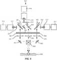
- An example of a scanned phosphor display disclosed in FIG. 2relies on the single ultraviolet or blue laser diode, the single scanning mirror and single phosphor plate.
- the light source for the displayis the blue or ultraviolet laser diode 210 that is driven by high frequency driver amplifier 211.
- the electrical modulation signals that are converted into light modulation signalsare provided by the processor 212 which receives the display content from video or other digital data source 214.
- the processor 212converts the standard video or image content into the format that is compatible with requirements of the scanning device 230 and the addressing of the display media that is composed of un-patterned phosphor plate 240.
- the monochromatic displayneeds only a single un-patterned plate.
- the full color displayrequires the phosphor plate 240 that is subdivided into or composed of three un-patterned phosphor segments (or sub-plates), red one, 241, green one 242 and blue one 243. Additional phosphor sub-plates can be added, such as orange sub-phosphor plate to enhance the color gamut of the displayed images.
- the different phosphor sub-plates 241, 242can be arranged in any convenient pattern, such as the row or two by two pattern with transmissive or reflective configuration.
- the coherent light generated by the laser diode 210is collimated by optics 220 and directed onto the scanning mirror 230.
- the scanneris typically bidirectional, biaxial actuator that permits angular scanning of the light beam over two dimensional raster. Unidirectional scanner represents another viable option. Another scanning option uses two uniaxial actuators for the full two dimensional image.
- the optical engine composed of the unpackaged laser diode 210, the collimated optics 220, the unpackaged scanning mirror 230 and the phosphor plate 240is enclosed in the hermetic or non-hermetic package that protects the components against particulate contamination.
- the optional hermetic packagecan be filled with inert gas, gas containing oxygen or other desired gas dopant with lower pressure than atmospheric pressure, compressed dry air, or contain low level of vacuum if low friction operation of the scanner is desirable for higher deflection angle operation.
- Packaging the phosphor plate inside the modulehas certain benefits with respect to form factor, reliability, and cost.
- a laser diodeis formed in gallium and nitrogen containing epitaxial layers that have been transferred from the native gallium and nitrogen containing substrates that are described in U.S. Patent Application No. 14/312,427 and U.S. Patent Publication No. 2015/0140710 .
- this technology of GaN transfercan enable lower cost, higher performance, and a more highly manufacturable process flow.
- the typical scanning mirrorcan be two dimensional Micro-Electro-Mechanical Systems (MEMS) electrostatically or electromagnetically driven scanner.
- MEMSMicro-Electro-Mechanical Systems
- the electrostatic comb MEMS scanner 230offers large deflection angles, high resonant frequencies and relatively high mechanical stiffness for good shock and vibration tolerance. When even higher resonant frequencies, higher scanning angles and higher immunity to shock and vibration are required, two dimensional electromagnetic scanning MEMS mirror 230 is used.
- Another embodimentuses two uniaxial scanning mirrors instead of one biaxial scanner.
- the scanning mirrorsare typically operated in the resonant mode or quasi-static mode and synchronization of their displacement with the digital content modulating the lasers is required.
- the active sensing of the deflection angles(not shown in the figure) is included in the system.
- sensorscan be of piezoelectric, piezoresistive, capacitive, optical or other types. Their signal is amplified and used in the feedback loop to synchronize the motion of mirrors with the digital display or video signals.
- the light image generated by laser beam scanning of un-patterned phosphorcan be viewed directly by the observer 260 or it can be re-imaged by the optical system 250 onto the appropriate optical screen 270.
- the optical system 250does not require any color light combiners, but for the full color imaging system, the optical system 250 includes also combining optics that are not shown in Fig. 2 for simplicity, but are shown in FIG. 5 and 6 below.
- the details of one un-patterned phosphor plateare included in FIG. 3a .
- the back side illumination 390impinges on the substrate 310 that is transparent to monochromatic laser illumination and is coated with antireflective thin film structure 320 on the illumination side.
- the highly reflective layer 330composed of the single film or multiple stack of high and low refractive index layers is used. The reflection is optimized for emission wavelengths of the phosphors so that almost all emitted light intensity is used in the forward direction. This coating is transparent at the excitation wavelength of the laser diode.
- the phosphor layer 340composed of powder films, single crystal phosphors or quantum dots are selected so that efficient phosphorescence occurs for the particular excitation wavelength and emission of desirable red, green and blue wavelengths.
- the plate 301can contain one, two, three or more phosphor sub-plates that are not shown in FIG. 3a .
- the optimized color gamutis achieved with the single phosphor or mixture of phosphors. Some examples of the phosphors for red, green, orange and blue, among others, are listed below.
- Images produced on the phosphor layer 340are re-imaged with the optical system 392.
- the phosphor platemay contain the heat sink in particular for high brightness systems.
- the heat sink for transmissive configurationis formed by materials that are very good thermal conductors but are optically transparent to the illumination light.
- the second architecture with the phosphor plate 302is presented in FIG. 3b .
- the excitation light 390is brought in from the front side of the phosphor surface.
- the scanned excitation light 390passes through dichroic mirror 351 and collection optics 350 and is directed to the phosphor plate 302 having the substrate 310.
- the phosphor 340is placed on the highly reflected layer 370 which in turn resides on the substrate 310.
- the light 391 emitted by the phosphors 340is collimated and imaged by the optical assembly 350 and directed to the screen or the observer by reflection from dichroic mirror 351 and by optional optical components 352.
- FIG. 3cshows the details of the full color phosphor plate 303 that comprises of the substrate 310 and phosphor films 341, 342 and 343 that are referred to here as sub-plates.
- the single layer or multilayer film stacks 371, 372 and 373 that reflect efficiently the phosphorescent light generated by three phosphors and also illumination light 390reside between the substrate 310 and phosphorescent films 341, 342 and 343.
- the single film stackcan be substituted for three different stacks with some loss of reflection efficiency for the emission spectra that cover three spectral regions.
- the reflective phosphor platesmay contain heat sink film that is placed below phosphors 341, 342, 343 or below reflective layers 371, 372, 373. In some cases, heat sink film functionality can be combined with reflection films.
- the full color display architecture 400 with three color sub-platesis shown in FIG. 4 .
- the modulated lightis generated by the laser diode 410 that is driven by the laser driver, video processing electronics according to input data represented by the unit 415 which has equivalent functionality to the unit 215 in FIG. 2 .
- the scanning mirror 430provides the scanning pattern over the phosphors 441, 442 and 443.
- the two state (on-off) mirror 473allows the excitation light to be guided onto the first phosphor 443 when it is in the on-state. When the mirror 473 is in the off-state and mirror 472 is switched into on-state, the excitation light is directed onto the second phosphor 442.
- the excitation lightfalls onto the fixed mirror 480 that brings the light onto the third phosphor 441.
- the light emitted by the phosphors 441, 442 and 443is imaged by the optical systems 451, 452, 453 and directed for recombination into one beam by using mirrors 461 and 462 and combining cube 460.
- the imagesare formed on the eye of the observer or on the screen 495.
- Additional design and performance flexibilitycan be achieved by adding additional light sources and the scanning mirrors to the basic architectures described above.
- the option with additional optical elementsis of particular interest when the displays or smart lighting are intended for high brightness applications that cannot be satisfied by the single light source with the highest available power.
- the architecture of such a designis shown in FIG. 5 .
- the display mediumis the same as disclosed in FIG. 3c with three phosphor segments 541, 542 and 543.
- the transmission, back side illuminationis selected here for illustration of one typical architecture, even though other illumination options can be used such as reflection, front side illumination in FIG. 3b .
- additional laser diodescan be added.
- Three laser diodes 511, 512 and 513 with ultraviolet or blue wavelengthmay serve as light sources.
- the laser diodesare driven with electronic circuits 515, 516 and 517. The elements of these circuits have been disclosed earlier, with description of FIG. 2 .
- the laser light from the laser diodes 511, 512 and 513is collimated with optical elements 521, 522 and 523 respectively.
- the collimated, modulated light trainsare directed to three scanning mirrors 531, 532 and 533 that address the phosphors 541, 542 and 543. This type of addressing is referred to herein as simultaneous color addressing.
- the data rates to modulate the laser diodescan be at least three times slower than color sequential addressing data rates disclosed in FIG. 4 .
- the scanning mirror resonant frequencies for the fast axiscan be three times lower than the frequencies required for sequential color addressing of FIG. 4 .
- Light emitted by phosphors 541, 542 and 543is collected by optical subsystems 551, 552 and 553 described earlier.
- the superposition of these three color beamsis accomplished by right angle static mirrors 561 and 563 and cube color combiner 560.
- the color images or videoare then directed to the screen 595 or directly to the observer.
- optical architecture of FIG. 5is very suitable for high brightness applications.
- the laser diodes 511, 512 and 513can be nominally the same lasers with the same emission wavelength.
- the power rating of the laser diodescan be selected so that desired brightness and color gamut are achieved on the screen.
- the laser diodes 511, 512 and 513can have different emission wavelengths that provide higher conversion efficiency of phosphor emission.
- the cooling of phosphors or their motion on color wheelis typically not required, as the energy input from the laser diodes is naturally distributed over the whole area of phosphors by scanning of these laser beams.
- Another embodimentplaces phosphor(s) directly on the scanning mirror surface.
- the separate phosphor plates 541, 542 and 543are not required in FIG. 5 .
- the blue laser diodecan be polar, semipolar, and non-polar.
- green laser diodecan be polar, semipolar, and non-polar.
- blue and/or green diodesare manufactured from bulk substrate containing gallium nitride material.
- the light sourcecomprises a single laser diode.
- the light sourcecomprises a blue laser diode that outputs blue laser beams.
- the light sourcealso includes one or more optical members that change the blue color of the laser beam.
- the one or more optical membersinclude phosphor material.
- the light sourcemay include laser diodes and/or Light Emitting Diodes (LEDs).
- the light sourceincludes laser diodes in different colors.
- the light sourceincludes one or more colored LEDs.
- light sourceincludes both laser diodes and LEDs.
- laser diodesare utilized in 3D display applications.
- 3D display systemsrely on the stereoscopic principle, where stereoscopic technology uses a separate device for person viewing the scene which provides a different image to the person's left and right eyes.
- Example of this technologyis shown in Fig. 6 .
- the architecturewhich is the simplest optically but more complex electrically is shown in FIG. 6 with the single 2D scanning mirror 630 and the single phosphor plate 641.
- the other architecturescomprise two 2D scanning mirrors and two phosphor plates that generate two images for two eyes independently but in synchronization.
- More complex optical architecturecan comprise six 2D scanning mirrors, six phosphor plate and three image combiners, where each two phosphor plates provide one color for the image. This architecture has the easiest requirements on data rates, scanning rates of the mirrors and bandwidth of the driving electronics.
- the architecture 600 of 3D displayfurther includes the light source 610 with the power modulating electronics 615.
- the light from the light source 610is collimated by optical components 620 and directed onto 2D biaxial mirror scanner 630.
- the light rastered by the scannerpasses through the dichroic mirror 660 and the optical assembly 651 that focuses the incident light on the phosphor plate 641 which is implemented here in the reflection configuration.
- One color displayrequires only a single color phosphor while the full color display requires at least three phosphor sub-plates that form the complete phosphor plate, as disclosed above in FIG. 3c .
- the mirror 672When the image is supposed to be directed to the left eye 695 of the observer, then the mirror 672 is in the on position.
- the mirror 672When the image is intended for the right eye 696 of the observer, the mirror 672 is in the off position and light is directed through the optical element 690. In that case, the light falls onto the fixed mirror 680 which reflects it through the lens 691 to the right eye 696 of the observer.
- the scanning mirrors 630 and 672are controlled by the electronic circuits 616 that receive the feedback signals from the sensors on the mirrors 630 and 680 about their positions.
- the servo circuits that are not shown in FIG. 6then adjust the electrical signals to the mirrors so that the video data that is streamed into the laser source 610 is synchronized with the mirror positions.
- the present inventionincludes a device and method configured on other gallium and nitrogen containing substrate orientations.
- the gallium and nitrogen containing substrateis configured on a family of planes including a ⁇ 20-21 ⁇ crystal orientation.
- ⁇ 20-21 ⁇is 14.9 degrees off of the m-plane towards the c-plane (0001).
- the miscut or off-cut angleis +/-17 degrees from the m-plane towards c-plane or alternatively at about the ⁇ 20-21 ⁇ crystal orientation plane.
- the present deviceincludes a laser stripe oriented in a projection of the c-direction, which is perpendicular to the a-direction (or alternatively on the m-plane, it is configured in the c-direction).
- the cleaved facetwould be the gallium and nitrogen containing face (e.g., GaN face) that is 1-5 degrees from a direction orthogonal to the projection of the c-direction (or alternatively, for the m-plane laser, it is the c-face).
- GaN substrateis associated with Group III-nitride based materials including GaN, InGaN, AlGaN, or other Group III containing alloys or compositions that are used as starting materials.
- the laser diodecan be enclosed in a suitable package.
- a suitable packagecan include those such as in TO-38 and TO-56 headers.
- Other suitable package designs and methodscan also exist, such as TO-9 and even non-standard packaging.
- the present devicecan be implemented in a co-packaging configuration such as those described in U.S. Provisional Application No. 61/347,800 .
- the present laser devicecan be configured in a variety of applications. Such applications include laser displays, metrology, communications, health care and surgery, information technology, and others.
- the present laser devicecan be provided in a laser display such as those described in U.S. Ser. No. 12/789,303 filed May 27, 2010 , which claims priority to U.S. Provisional Nos. 61/182,105 filed May 29, 2009 and 61/182,106 filed May 29, 2009 .
- U.S. Ser. No. 12/789,303 filed May 27, 2010which claims priority to U.S. Provisional Nos. 61/182,105 filed May 29, 2009 and 61/182,106 filed May 29, 2009 .
- a method and deviceare provided for emitting electromagnetic radiation using non-polar or semipolar gallium containing substrates such as GaN, AlN, InN, InGaN, AlGaN, and AlInGaN, and others.
- the inventioncan be applied to optical devices, lasers, light emitting diodes, solar cells, photoelectrochemical water splitting and hydrogen generation, photodetectors, integrated circuits, and transistors, among other devices.
- a phosphor, or phosphor blend or phosphor single crystalcan be selected from one or more of (Y, Gd, Tb, Sc, Lu, La).sub.3(Al, Ga, In).sub.5O.sub.12:Ce.sup.3+, SrGa.sub.2S.sub.4:Eu.sup.2+, SrS:Eu.sup.2+, and colloidal quantum dot thin films comprising CdTe, ZnS, ZnSe, ZnTe, CdSe, or CdTe.
- a phosphoris capable of emitting substantially red light, wherein the phosphor is selected from one or more of the group consisting of (Gd,Y,Lu,La).sub.2O.sub.3:Eu.sup.3+, Bi.sup.3+; (Gd,Y,Lu,La).sub.2O.sub.2S:Eu.sup.3+, Bi.sup.3+; (Gd,Y,Lu,La)VO.sub.4:Eu.sup.3+, Bi.sup.3+; Y.sub.2(O,S).sub.3: Eu.sup.3+; Ca.sub.1-xMo.sub.1-ySi.sub.yO.sub.4: where 0.05.ltoreq.x.ltoreq.0.5, 0.ltoreq.y.ltoreq.0.1; (Li,Na,K).sub.5Eu(W,Mo)O.sub.4; (Li,
- the laser or LED devicecan be configured in a variety of packages such as cylindrical, surface mount, power, lamp, flip-chip, star, array, strip, or geometries that rely on lenses (silicone, glass) or sub-mounts (ceramic, silicon, metal, composite).
- the packagecan be any variations of these packages.
- the packaged devicecan include other types of optical and/or electronic devices.
- the optical devicescan be OLED, a laser, a nanoparticle optical device, and others.
- the electronic devicecan include an integrated circuit, a sensor, a micro-machined electronic mechanical system, or any combination of these, and the like.
- the packaged devicecan be coupled to a rectifier to convert alternating current power to direct current, which is suitable for the packaged device.
- the rectifiercan be coupled to a suitable base, such as an Edison screw such as E27 or E14, bipin base such as MR16 or GU5.3, or a bayonet mount such as GU10, or others.
- the rectifiercan be spatially separated from the packaged device.
- the present packaged devicecan be provided in a variety of applications. In a preferred embodiment, the application is general lighting, which includes buildings for offices, housing, outdoor lighting, stadium lighting, and others.
- the applicationscan be for display, such as those used for computing applications, televisions, flat panels, micro-displays, and others. Still further, the applications can include automotive, gaming, and others.
- the present devicesare configured to achieve spatial uniformity. That is, diffusers can be added to the encapsulant to achieve spatial uniformity.
- the diffuserscan include TiO.sub.2, CaF.sub.2, SiO.sub.2, CaCO.sub.3, BaSO.sub.4, and others, which are optically transparent and have a different index than the encapsulant causing the light to reflect, refract, and scatter to make the far field pattern more uniform.
- the diffuserscan include TiO.sub.2, CaF.sub.2, SiO.sub.2, CaCO.sub.3, BaSO.sub.4, and others, which are optically transparent and have a different index than the encapsulant causing the light to reflect, refract, and scatter to make the far field pattern more uniform.
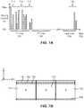
- the addressing of the phosphor platescan be performed in multiple ways, as outlined in FIG. 7 .
- the first addressing optionis color sequential, line by line alternative, with fast scanning in one direction (e.g., fast x direction) and slower scanning in the second direction (e.g., slow y direction) .
- the scanning mirror 230undergoes the line by line raster over the full width of the phosphor plate 240 in back and forth manner. If the phosphor plate 240 has three distinct RGB phosphors 241, 242 and 243, then the driving waveform will be as schematically shown in FIG.
- the first set of driving currents 711generates the corresponding desired laser intensities on the first line 761 of the red sub-plate 741
- the second set of driving currents 712that generates the desired laser intensities on the first line 761 of the green sub-plate 742
- the third set of driving currents 713 for the blue sub-plate 743When the second line 762 of the display image is being formed using the small displacement of the scanner along the slow y axis and another scan of the mirror in the opposite x direction, the second set of driving current waveforms is supplied to the laser diode to form the second line 762 of the image in the reverse sequence with blue, green and red.
- This addressing processis continued until the full image frame has been generated with the last line 769 having the last set of current pulses 723 for blue phosphor plate.
- the addressingis line by line, color sequential addressing. Multiple lasers can be combined in such configurations, for applications requiring higher optical output.
- the addressing schemecan be altered to accommodate frame by frame, color sequential addressing.
- the first color framesuch as red frame is fully defined, followed by the green and blue frames.
- the scanning mirror 230scans over the first phosphor (e.g., red) 741 completely and then continues scanning over the second phosphor (e.g., green) 742 fully and it completes the first color image frame by scanning over the full third phosphor (e.g., blue) 743 plate.
- the sequencing of the phosphor illuminationcan be optimized for thermal performance of the phosphor, to avoid overheating and to maximize the efficiency and reliability of the system.
- the smart dynamic illumination system 800based on disclosed illumination technology and the display or sensor technologies is presented in FIG. 8 , which shows the key architectural blocks of the system.
- the illumination subsystem 810can be white, one color or multicolor, as described in FIG. 2 to 5 .
- the illumination beam 820 or 821is directed toward the specific target 830 or background 870 that might contain the intended target to be followed with illumination beam.
- the detection subsystem 840can be a simple multi-element array of photosensors that respond in the visible part of the spectrum (0.4 to 0.7 um), such as the small CMOS or CCD array, or infrared spectrum, such as infrared sensor array or microbolometer array sensitive at spectral wavelengths from 0.3 to 15 um.
- the subsystem 840can be the full imaging array, sensitive in visible or infrared part of the spectrum.
- Other motion sensorsthat are based on non-imaging principles can also be used.
- the motion related signals or full visible or infrared imagesare analyzed with the processing electronics 850 and the data are directed to the servo control electronics 860.
- the servo subsystem 860generates the feedback signals and controls the scanning mirror(s) and lasers of illumination system 810. In this manner, the target can be followed with dynamic illumination, including the control of the intensity, color and time duration of the illumination as shown in FIG. 8 .
- the light 822 reflected and scattered by the targetchanges to the light beams 823.
- the change in the light beams or the images that they represent,are detected by the detection subsystem and fed into the processing electronics 850 and servo control 860 which controls the illumination beams by moving them from the position 830 to the position 831, effectively keeping the illumination beam directed on the target at all times.
- the illuminationis outside of the visible spectrum, the target may not be aware that it is monitored and followed which may be advantageous in some security applications.
- the complete dynamic illumination systemcan be mounted on the stationary platforms in offices, homes, galleries, etc. or can be employed in the movable systems such as automobiles, planes and drones.
Landscapes
- Physics & Mathematics (AREA)
- Engineering & Computer Science (AREA)
- Optics & Photonics (AREA)
- Multimedia (AREA)
- Signal Processing (AREA)
- General Physics & Mathematics (AREA)
- Microelectronics & Electronic Packaging (AREA)
- General Engineering & Computer Science (AREA)
- Mechanical Optical Scanning Systems (AREA)
- Semiconductor Lasers (AREA)
- Mechanical Light Control Or Optical Switches (AREA)
- Optical Filters (AREA)
- Projection Apparatus (AREA)
- Transforming Electric Information Into Light Information (AREA)
- Video Image Reproduction Devices For Color Tv Systems (AREA)
- Control Of Indicators Other Than Cathode Ray Tubes (AREA)
Description
- Large displays are becoming increasingly popular and are expected to gain further traction in the coming years as Liquid Crystal Displays (LCD) get cheaper for television (TV) and digital advertising becomes more popular at gas stations, malls, and coffee shops. Substantial growth (e.g., over 40%) has been seen in the past several years for large format displays (e.g., >40 inch TVs), and consumers have grown accustomed to larger displays for laptops and Personal Computers (PC) as well. As more viewing content is available via mobile devices such as TV, internet and video, displays in handheld consumer electronics remain small (<6 inch) with the keyboard, camera, and other features competing for space and power.
- Additionally, smart lighting is emerging as a large opportunity within the current $80B lighting market, where sensors and connectivity are introduced into the light source, as well as dynamic features related to the illumination.
- Existing illumination sources have substantial shortcomings in meeting the needs of these important applications. Specifically, the delivered lumens per electrical watt of power consumption is typically quite low, due to the low efficiency of the source, the low spatial brightness of the source and very low optical efficiency of optical engines. Another key drawback is in the cost per delivered lumen, which, for existing sources, is typically high because of the poor optical efficiency. Another key shortcoming of the existing sources relates to the lack of dynamic functionality, specifically in their limited ability to generate dynamic spatial and color patterns in a compact form factor with high efficiency and low cost.
- Therefore, improved systems for displaying images and video, and smart lighting are desired.
US 2006/0221022 describes fluorescent screens and display systems and devices based on such screens using at least one excitation optical beam to excite one or more fluorescent materials on a screen which emit light to form images. The fluorescent materials may include phosphor materials and non-phospor materials such as quantum dots. A screen may include a multi-layer dichroic layer. Vector scanner systems may be constructed using screens with one or more fluorescent materials.- The present invention is set out in the appended claims, Described herein are techniques for laser lighting. Merely by way of example, the disclosure can be applied to applications such as white lighting, white spot lighting, flash lights, automobile headlights, all-terrain vehicle lighting, light sources used in recreational sports such as biking, surfing, running, racing, boating, light sources used for safety, drones, robots, counter measures in defense applications, multi-colored lighting, lighting for flat panels, medical, metrology, beam projectors and other displays, high intensity lamps, spectroscopy, entertainment, theater, music, and concerts, analysis fraud detection and/or authenticating, tools, water treatment, laser dazzlers, targeting, communications, transformations, transportations, leveling, curing and other chemical treatments, heating, cutting and/or ablating, pumping other optical devices, other optoelectronic devices and related applications, and source lighting and the monochromatic, black and white or full color projection displays and the like.
- Optical engines with single laser light source, scanning mirror and un-patterned phosphor as well as engines with multiple lasers, scanning mirrors and un-patterned phosphors are disclosed. Multiple re-imaged phosphor architectures with transmission and reflection configurations, and color line and frame sequential addressing and parallel simultaneous addressing are described. These high power efficiency and small engines do not require any de-speckling for high image quality and offer adjustable, on demand resolution and color gamut for projection displays and smart lighting applications.
- In an example, the present disclosure provides an optical engine apparatus. The apparatus has a laser diode device, the laser diode device characterized by a wavelength ranging from 300 to 2000 nm or any variations thereof. In an example, the apparatus has a lens coupled to an output of the laser diode device and a scanning mirror device operably coupled to the laser diode device. In an example, the apparatus has an un-patterned phosphor plate coupled to the scanning mirror and configured with the laser device; and a spatial image formed on the un-patterned phosphor plate configured by a modulation of the laser and movement of the scanning mirror device.
- In an alternative example, the device has an optical engine apparatus. The apparatus has a laser diode device. In an example, the laser diode device is characterized by a wavelength. In an example, the apparatus has a lens coupled to an output of the laser diode device. The apparatus has a scanning mirror device operably coupled to the laser diode device and an un-patterned phosphor plate coupled to the scanning mirror and configured with the laser device. The apparatus has a spatial image formed on a portion of the un-patterned phosphor plate configured by a modulation of the laser and movement of the scanning mirror device. In a preferred embodiment, the apparatus has a resolution associated with the spatial image, the resolution being selected from one of a plurality of pre-determined resolutions. In an example, the resolution is provided by control parameter associated with the spatial image.
- In an example, the apparatus has a color or colors associated with the spatial image, the color or colors being associated with the modulation of the laser device and movement of the scanning mirror device. In an example, the apparatus has another spatial image formed on the second color un-patterned phosphor plate. In an example, the other spatial image having another or same resolution and different color. In an example, the other spatial image is output concurrently or simultaneously with the spatial image on the first color un-patterned phosphor plate. In an example, the spatial image is characterized by a time constant. In an example, the control parameter is provided by a controller coupled to the laser diode device and the scanning mirror device. In an example, the spatial image is speckle free.
- In an example, the apparatus has an efficiency of greater than 10% to 80% based upon an input power to the laser diode device and an output of the spatial image. In an example, the apparatus has a direct view of the spatial image by a user.
- In an example, the present disclosure has an optical engine apparatus. The apparatus has a laser diode device. In an example, the laser diode device characterized by a wavelength ranging from 300 to 2000 nm, although there can be variations. In an example, the apparatus has a lens coupled to an output of the laser diode device. The apparatus has a scanning mirror device operably coupled to the laser diode device. The apparatus has a beam path provided from the scanning mirror. The apparatus has a first color un-patterned phosphor plate coupled to the scanning mirror via the beam path and configured with the laser device, a second color un-patterned phosphor plate coupled to the scanning mirror via the beam path and configured with the laser device, and a third color un-patterned phosphor plate coupled to the scanning mirror via the beam path and configured with the laser device. In an example, the apparatus has a spatial image formed on a portion of either the first color un-patterned phosphor plate, the second color un-patterned phosphor plate, or the third color un-patterned phosphor plate, or over all three un-patterned phosphor plates configured by a modulation of the laser and movement of the scanning mirror device.
- In an example, the apparatus has a first blocking mirror configured in a first portion of the beam path to configure the beam path to the first un-patterned phosphor plate; a second blocking mirror configured to a second portion of the beam path to configure the beam path to the second un-patterned phosphor plate.
- In an example, the apparatus has a controller coupled to the laser diode device and the scanning mirror device, and configured to generate the spatial image on the portion of the un-patterned phosphor.
- In an example, the un-patterned phosphor plate comprises a multi-element phosphor species. In an example, the multi-element phosphor species comprises a red phosphor, a green phosphor, and a blue phosphor.
- In an example, the un-patterned phosphor plate comprises a plurality of color phosphor sub-plates.
- In an example, the scanning mirror device comprises a plurality of scanning mirrors. In an example, the un-patterned phosphor is included on the scanning mirror. In an example, an three dimensional (3D) display apparatus comprises one or more laser diodes, one or more scanning mirrors and one or more un-patterned phosphors to generate two stereoscopic images for the left and right eyes.
- In an example, the apparatus is configured with a display system. In an example, the un-patterned phosphor plate comprises a red phosphor, a green phosphor, or a blue phosphor within a spatial region of the un-patterned phosphor plate.
- In an example, the apparatus has a heat sink device coupled to the un-patterned phosphor plate such that thermal energy is transferred and removed using the heat sink device; and wherein the un-patterned phosphor plate includes at least one of a transmissive phosphor species or a reflective phosphor species.
- Various benefits are achieved over pre-existing techniques using the present invention. In particular, the present invention enables a cost-effective projection systems that utilize efficient light sources and result in high overall optical efficiency of the lighting or display system. In a specific embodiment, the light source can be manufactured in a relatively simple and cost effective manner. Depending upon the embodiment, the present apparatus and method can be manufactured using conventional materials and/or methods according to one of ordinary skill in the art. In one or more embodiments, the laser device is capable of multiple wavelengths. Of course, there can be other variations, modifications, and alternatives. Depending upon the embodiment, one or more of these benefits may be achieved. These and other benefits may be described throughout the present specification and more particularly below.
- The present invention achieves these benefits and others in the context of known process technology. However, a further understanding of the nature and advantages of the present invention may be realized by reference to the latter portions of the specification and attached drawings.
FIG. 1 is a simplified schematic diagram of the prior art, conventional scanning mirror display.FIG. 2 is a simplified schematic diagram of novel architecture of the optical engine and addressing electronics of the display with scanning mirror and un-patterned phosphor plate according to an example.FIG. 3a illustrates the optical configuration with backside, transmission illumination and details of phosphor plate;FIG. 3b illustrates the optical configuration with front side, perpendicular reflective illumination and details of the corresponding phosphor plate according to examples; andFIG. 3c illustrates a full color phosphor plate.FIG. 4 illustrates an optical architecture with one laser diode, one scanning mirror and two uniaxial on-off mirrors according to an example.FIG. 5 illustrates an optical architecture with three laser diodes and three scanning mirrors according to an example.FIG. 6 illustrates a three dimensional (3D) optical architecture with a laser diode and phosphor plate configured to a scanning mirror according to an example.FIG. 7a illustrates the driving waveforms for addressing of un-patterned phosphor display; andFIG. 7b illustrates the scanning line pattern over three un-patterned phosphor plates according to examples.FIG. 8 illustrates a system for dynamic lighting with the feedback mechanism to follow the moving target according to an example.- Techniques for laser lighting are provided.
- This description relates to optical and electrical designs, architecture and implementation of smart lighting and displays. The optical architecture is based on the single or multiple laser diodes, single or multiple scanning mirrors and single or multiple un-patterned phosphor plates.
- As background, conventional displays use white light illumination and array of color filters and addressable Liquid Crystal Display (LCD) pixels on the panels, with pixels being turned on or off with or without light intensity control by addressing electronics. Another type of displays is formed by array of addressable pixels that generate light emission by electroluminescence (Organic Light Emitting Diode - OLED array). Yet another type of display is created by addressable array of deflectable micromirrors that reflect the color sequential, time division multiplexed light selectively to projection optics and a screen. Additionally, another type of color display that does not require the matrix of addressable elements is based on three color light sources and the biaxial scanning mirror that allows formation of images by scanning in two directions while three lasers or other light sources are directly modulated by driving currents. In addition, patterned phosphor plate with red, green and blue array of phosphor pixels can be addressed by laser light incident on scanning mirrors while the light intensities are controlled by laser drivers. Illumination patterns can be viewed directly, or re-imaged with an optical system to a desired surface.
- The commonality of the matrix array display products is the fixed resolution of the displayed content, fixed color gamut, low power efficiency and optical and electrical complexity. The direct and re-imaged scanning mirror displays that do not use matrices of colored phosphor pixels offer adjustable resolution, higher power efficiency, and a compact footprint, but suffer from image speckle that is the result of coherent nature of laser light sources required for these displays, and also from safety issues, regulatory complexity, and high cost since 3 types of lasers with different wavelengths are required.
- This disclosure describes novel displays and smart lighting that have resolution and color gamut on demand, very high power efficiency, no speckle and optical and electrical simplicity, miniature packaging, minimum number of active elements, and minimal safety and regulatory concerns. The multiple optical engine embodiments and several addressing schemes are disclosed.
- A prior art scanning mirror display architecture is outlined in
FIG. 1 . An example can be found in United States Patent No.9,100,590, in the name of Raring , et al. issued August 4, 2015 - According to an example, a projection apparatus is provided. The projection apparatus includes a housing having an aperture. The apparatus also includes an
input interface 110 for receiving one or more frames of images. The apparatus includes avideo processing module 120. Additionally, the apparatus includes a laser source. The laser source includes ablue laser diode 131, agreen laser diode 132, and ared laser diode 133. The blue laser diode is fabricated on a nonpolar or semipolar oriented Ga-containing substrate and has a peak operation wavelength of about 430 to 480 nm, although other wavelengths can be used. The green laser diode is fabricated on a nonpolar or semipolar oriented Ga-containing substrate and has a peak operation wavelength of about 490 nm to 540 nm. The red laser could be fabricated from AlInGaP withwavelengths 610 to 700 nm. The laser source is configured to produce a laser beam by combining outputs from the blue, green, and red laser diodes usingdichroic mirrors laser driver module 150 coupled to the laser source. The laser driver module generates three drive currents based on a pixel from the one or more frames of images. Each of the three drive currents is adapted to drive a laser diode. The apparatus also includes a Micro-Electro-Mechanical System (MEMS)scanning mirror 160, or "flying mirror", configured to project the laser beam to a specific location through the aperture resulting in asingle picture 170. By rastering the pixel in two dimensions, a complete image is formed. The apparatus includes an optical member provided within proximity of the laser source, the optical member being adapted to direct the laser beam to the MEMS scanning mirror. The apparatus includes a power source electrically coupled to the laser source and the MEMS scanning mirror. - An example of a scanned phosphor display disclosed in
FIG. 2 relies on the single ultraviolet or blue laser diode, the single scanning mirror and single phosphor plate. The light source for the display is the blue orultraviolet laser diode 210 that is driven by highfrequency driver amplifier 211. The electrical modulation signals that are converted into light modulation signals are provided by theprocessor 212 which receives the display content from video or otherdigital data source 214. Theprocessor 212 converts the standard video or image content into the format that is compatible with requirements of thescanning device 230 and the addressing of the display media that is composed ofun-patterned phosphor plate 240. The monochromatic display needs only a single un-patterned plate. The full color display requires thephosphor plate 240 that is subdivided into or composed of three un-patterned phosphor segments (or sub-plates), red one, 241, green one 242 and blue one 243. Additional phosphor sub-plates can be added, such as orange sub-phosphor plate to enhance the color gamut of the displayed images. Thedifferent phosphor sub-plates - The coherent light generated by the
laser diode 210 is collimated byoptics 220 and directed onto thescanning mirror 230. The scanner is typically bidirectional, biaxial actuator that permits angular scanning of the light beam over two dimensional raster. Unidirectional scanner represents another viable option. Another scanning option uses two uniaxial actuators for the full two dimensional image. - The optical engine composed of the
unpackaged laser diode 210, the collimatedoptics 220, theunpackaged scanning mirror 230 and thephosphor plate 240 is enclosed in the hermetic or non-hermetic package that protects the components against particulate contamination. The optional hermetic package can be filled with inert gas, gas containing oxygen or other desired gas dopant with lower pressure than atmospheric pressure, compressed dry air, or contain low level of vacuum if low friction operation of the scanner is desirable for higher deflection angle operation. Packaging the phosphor plate inside the module has certain benefits with respect to form factor, reliability, and cost. - A laser diode is formed in gallium and nitrogen containing epitaxial layers that have been transferred from the native gallium and nitrogen containing substrates that are described in
U.S. Patent Application No. 14/312,427 andU.S. Patent Publication No. 2015/0140710 . As an example, this technology of GaN transfer can enable lower cost, higher performance, and a more highly manufacturable process flow. - The typical scanning mirror can be two dimensional Micro-Electro-Mechanical Systems (MEMS) electrostatically or electromagnetically driven scanner. The electrostatic
comb MEMS scanner 230 offers large deflection angles, high resonant frequencies and relatively high mechanical stiffness for good shock and vibration tolerance. When even higher resonant frequencies, higher scanning angles and higher immunity to shock and vibration are required, two dimensional electromagneticscanning MEMS mirror 230 is used. Another embodiment uses two uniaxial scanning mirrors instead of one biaxial scanner. The scanning mirrors are typically operated in the resonant mode or quasi-static mode and synchronization of their displacement with the digital content modulating the lasers is required. The active sensing of the deflection angles (not shown in the figure) is included in the system. It can be accomplished by incorporation of the sensors on the hinges of the scanning mirrors. These sensors can be of piezoelectric, piezoresistive, capacitive, optical or other types. Their signal is amplified and used in the feedback loop to synchronize the motion of mirrors with the digital display or video signals. - The light image generated by laser beam scanning of un-patterned phosphor can be viewed directly by the
observer 260 or it can be re-imaged by theoptical system 250 onto the appropriateoptical screen 270. For one color imaging system, theoptical system 250 does not require any color light combiners, but for the full color imaging system, theoptical system 250 includes also combining optics that are not shown inFig. 2 for simplicity, but are shown inFIG. 5 and6 below. - The details of one un-patterned phosphor plate are included in
FIG. 3a . Theback side illumination 390 impinges on thesubstrate 310 that is transparent to monochromatic laser illumination and is coated with antireflectivethin film structure 320 on the illumination side. On the phosphor side of the substrate, the highlyreflective layer 330 composed of the single film or multiple stack of high and low refractive index layers is used. The reflection is optimized for emission wavelengths of the phosphors so that almost all emitted light intensity is used in the forward direction. This coating is transparent at the excitation wavelength of the laser diode. Thephosphor layer 340 composed of powder films, single crystal phosphors or quantum dots are selected so that efficient phosphorescence occurs for the particular excitation wavelength and emission of desirable red, green and blue wavelengths. The plate 301 can contain one, two, three or more phosphor sub-plates that are not shown inFIG. 3a . The optimized color gamut is achieved with the single phosphor or mixture of phosphors. Some examples of the phosphors for red, green, orange and blue, among others, are listed below. Images produced on thephosphor layer 340 are re-imaged with theoptical system 392. The phosphor plate may contain the heat sink in particular for high brightness systems. The heat sink for transmissive configuration is formed by materials that are very good thermal conductors but are optically transparent to the illumination light. - The second architecture with the
phosphor plate 302 is presented inFIG. 3b . In this case, theexcitation light 390 is brought in from the front side of the phosphor surface. The scanned excitation light 390 passes throughdichroic mirror 351 andcollection optics 350 and is directed to thephosphor plate 302 having thesubstrate 310. Thephosphor 340 is placed on the highly reflectedlayer 370 which in turn resides on thesubstrate 310. The light 391 emitted by thephosphors 340 is collimated and imaged by theoptical assembly 350 and directed to the screen or the observer by reflection fromdichroic mirror 351 and by optionaloptical components 352. FIG. 3c shows the details of the fullcolor phosphor plate 303 that comprises of thesubstrate 310 andphosphor films illumination light 390 reside between thesubstrate 310 andphosphorescent films phosphors reflective layers - The full
color display architecture 400 with three color sub-plates is shown inFIG. 4 . The modulated light is generated by thelaser diode 410 that is driven by the laser driver, video processing electronics according to input data represented by theunit 415 which has equivalent functionality to theunit 215 inFIG. 2 . Thescanning mirror 430 provides the scanning pattern over thephosphors mirror 473 allows the excitation light to be guided onto thefirst phosphor 443 when it is in the on-state. When themirror 473 is in the off-state andmirror 472 is switched into on-state, the excitation light is directed onto thesecond phosphor 442. When both mirrors 473 and 472 are in the off-state, the excitation light falls onto the fixedmirror 480 that brings the light onto thethird phosphor 441. The light emitted by thephosphors optical systems mirrors cube 460. The images are formed on the eye of the observer or on thescreen 495. - Additional design and performance flexibility can be achieved by adding additional light sources and the scanning mirrors to the basic architectures described above. The option with additional optical elements is of particular interest when the displays or smart lighting are intended for high brightness applications that cannot be satisfied by the single light source with the highest available power. The architecture of such a design is shown in
FIG. 5 . The display medium is the same as disclosed inFIG. 3c with threephosphor segments FIG. 3b . When higher display brightness than brightness that can be provided with the highest single laser power output and phosphor combination is needed, additional laser diodes can be added. Threelaser diodes electronic circuits FIG. 2 . The laser light from thelaser diodes optical elements phosphors FIG. 4 . Moreover, the scanning mirror resonant frequencies for the fast axis can be three times lower than the frequencies required for sequential color addressing ofFIG. 4 . Light emitted byphosphors optical subsystems static mirrors cube color combiner 560. The color images or video are then directed to thescreen 595 or directly to the observer. - This embodiment has more optical components but less challenging requirements on laser modulation frequencies and scanning angles. In addition, optical architecture of
FIG. 5 is very suitable for high brightness applications. Thelaser diodes laser diodes FIG. 1 that form images with highly parallel beams and require significant laser safety measures to avoid accidental direct eye exposures. - Another embodiment places phosphor(s) directly on the scanning mirror surface. In this case, the
separate phosphor plates FIG. 5 . - Different elements and features from the described architectures can be combined in other ways to create other designs suitable for the specific applications. In various embodiment, the blue laser diode can be polar, semipolar, and non-polar. Similarly, green laser diode can be polar, semipolar, and non-polar. For example, blue and/or green diodes are manufactured from bulk substrate containing gallium nitride material. For example, following combinations of laser diodes are provided, but there could be others: Blue polar+Green nonpolar+Red* AlInGaP, Blue polar+Green semipolar+Red* AlInGaP, Blue polar+Green polar+Red* AlInGaP, Blue semipolar+Green nonpolar+Red* AlInGaP, Blue semipolar+Green semipolar+Red* AlInGaP, Blue semipolar+Green polar+Red* AlInGaP, Blue nonpolar+Green nonpolar+Red* AlInGaP, Blue nonpolar+Green semipolar+Red* AlInGaP, Blue nonpolar+Green polar+Red* AlInGaP. In an alternative embodiment, the light source comprises a single laser diode. For example, the light source comprises a blue laser diode that outputs blue laser beams. The light source also includes one or more optical members that change the blue color of the laser beam. For example, the one or more optical members include phosphor material. It is to be appreciated that the light source may include laser diodes and/or Light Emitting Diodes (LEDs). In one embodiment, the light source includes laser diodes in different colors. In another embodiment, the light source includes one or more colored LEDs. In yet another embodiment, light source includes both laser diodes and LEDs.
- In various embodiments, laser diodes are utilized in 3D display applications. Typically, 3D display systems rely on the stereoscopic principle, where stereoscopic technology uses a separate device for person viewing the scene which provides a different image to the person's left and right eyes. Example of this technology is shown in
Fig. 6 . Even though several different embodiments are useful. The architecture which is the simplest optically but more complex electrically is shown inFIG. 6 with the single2D scanning mirror 630 and thesingle phosphor plate 641. The other architectures comprise two 2D scanning mirrors and two phosphor plates that generate two images for two eyes independently but in synchronization. More complex optical architecture can comprise six 2D scanning mirrors, six phosphor plate and three image combiners, where each two phosphor plates provide one color for the image. This architecture has the easiest requirements on data rates, scanning rates of the mirrors and bandwidth of the driving electronics. - The
architecture 600 of 3D display further includes thelight source 610 with thepower modulating electronics 615. The light from thelight source 610 is collimated byoptical components 620 and directed onto 2Dbiaxial mirror scanner 630. The light rastered by the scanner passes through thedichroic mirror 660 and theoptical assembly 651 that focuses the incident light on thephosphor plate 641 which is implemented here in the reflection configuration. One color display requires only a single color phosphor while the full color display requires at least three phosphor sub-plates that form the complete phosphor plate, as disclosed above inFIG. 3c . The light emitted by thephosphor 641 in re-imaged with the optical assemble 651, reflected from thedichroic mirror 660 onto two state (on-off)MEMS mirror 672. When the image is supposed to be directed to theleft eye 695 of the observer, then themirror 672 is in the on position. When the image is intended for theright eye 696 of the observer, themirror 672 is in the off position and light is directed through theoptical element 690. In that case, the light falls onto the fixedmirror 680 which reflects it through thelens 691 to theright eye 696 of the observer. The scanning mirrors 630 and 672 are controlled by theelectronic circuits 616 that receive the feedback signals from the sensors on themirrors FIG. 6 then adjust the electrical signals to the mirrors so that the video data that is streamed into thelaser source 610 is synchronized with the mirror positions. - In other embodiments, the present invention includes a device and method configured on other gallium and nitrogen containing substrate orientations. In a specific embodiment, the gallium and nitrogen containing substrate is configured on a family of planes including a {20-21} crystal orientation. In a specific embodiment, {20-21} is 14.9 degrees off of the m-plane towards the c-plane (0001). As an example, the miscut or off-cut angle is +/-17 degrees from the m-plane towards c-plane or alternatively at about the {20-21} crystal orientation plane. As another example, the present device includes a laser stripe oriented in a projection of the c-direction, which is perpendicular to the a-direction (or alternatively on the m-plane, it is configured in the c-direction). In one or more embodiments, the cleaved facet would be the gallium and nitrogen containing face (e.g., GaN face) that is 1-5 degrees from a direction orthogonal to the projection of the c-direction (or alternatively, for the m-plane laser, it is the c-face).
- As used herein, the term GaN substrate is associated with Group III-nitride based materials including GaN, InGaN, AlGaN, or other Group III containing alloys or compositions that are used as starting materials. Such starting materials include polar GaN substrates (i.e., substrate where the largest area surface is nominally an (h k 1) plane wherein h=k=0, and 1 is non-zero), non-polar GaN substrates (i.e., substrate material where the largest area surface is oriented at an angle ranging from about 80-100 degrees from the polar orientation described above towards an (h k l) plane wherein 1=0, and at least one of h and k is non-zero) or semi-polar GaN substrates (i.e., substrate material where the largest area surface is oriented at an angle ranging from about 0.1 to 80 degrees or 110-179.9 degrees from the polar orientation described above towards an (h k l) plane wherein l=0, and at least one of h and k is non-zero). The laser diode can be enclosed in a suitable package. Such package can include those such as in TO-38 and TO-56 headers. Other suitable package designs and methods can also exist, such as TO-9 and even non-standard packaging. In a specific embodiment, the present device can be implemented in a co-packaging configuration such as those described in
U.S. Provisional Application No. 61/347,800 - In other embodiments, some or all components of these optical engines, including the bare (unpackaged) light sources and scanning mirrors can be packaged in the common package hermetically or non-hermetically, with or without specific atmosphere in the package. In other embodiments, the present laser device can be configured in a variety of applications. Such applications include laser displays, metrology, communications, health care and surgery, information technology, and others. As an example, the present laser device can be provided in a laser display such as those described in
U.S. Ser. No. 12/789,303 filed May 27, 2010 U.S. Provisional Nos. 61/182,105 filed May 29, 2009 61/182,106 filed May 29, 2009 - In an example, a method and device are provided for emitting electromagnetic radiation using non-polar or semipolar gallium containing substrates such as GaN, AlN, InN, InGaN, AlGaN, and AlInGaN, and others. The invention can be applied to optical devices, lasers, light emitting diodes, solar cells, photoelectrochemical water splitting and hydrogen generation, photodetectors, integrated circuits, and transistors, among other devices.
- In an example, a phosphor, or phosphor blend or phosphor single crystal can be selected from one or more of (Y, Gd, Tb, Sc, Lu, La).sub.3(Al, Ga,
In).sub.5O.sub.12:Ce.sup.3+, SrGa.sub.2S.sub.4:Eu.sup.2+, SrS:Eu.sup.2+, and colloidal quantum dot thin films comprising CdTe, ZnS, ZnSe, ZnTe, CdSe, or CdTe. In an example, a phosphor is capable of emitting substantially red light, wherein the phosphor is selected from one or more of the group consisting of (Gd,Y,Lu,La).sub.2O.sub.3:Eu.sup.3+, Bi.sup.3+; (Gd,Y,Lu,La).sub.2O.sub.2S:Eu.sup.3+, Bi.sup.3+; (Gd,Y,Lu,La)VO.sub.4:Eu.sup.3+, Bi.sup.3+; Y.sub.2(O,S).sub.3: Eu.sup.3+; Ca.sub.1-xMo.sub.1-ySi.sub.yO.sub.4: where 0.05.ltoreq.x.ltoreq.0.5, 0.ltoreq.y.ltoreq.0.1; (Li,Na,K).sub.5Eu(W,Mo)O.sub.4; (Ca,Sr)S:Eu.sup.2+; SrY.sub.2S.sub.4:Eu.sup.2+; CaLa.sub.2S.sub.4:Ce.sup.3+; (Ca,Sr)S:Eu.sup.2+; 3.5MgO*0.5MgF.sub.2*GeO.sub.2:Mn.sup.4+ (MFG); (Ba,Sr,Ca)Mg.sub.xP.sub.2O.sub.7:Eu.sup.2+, Mn.sup.2+; (Y,Lu).sub.2WO.sub.6:Eu.sup.3+, Mo.sup.6+; (Ba,Sr,Ca).sub.3Mg.sub.xSi.sub.2O.sub.8:Eu.sup.2+, Mn.sup.2+, wherein 1<x.ltoreq.2; (RE.sub.1-yCe.sub.y)Mg.sub.2-xLi.sub.xSi.sub.3-xPxO.sub.12, where RE is at least one of Sc, Lu, Gd, Y, and Tb, 0.0001<x<0.1 and 0.001<y<0.1; (Y, Gd, Lu, La).sub.2-xEu.sub.xW.sub.1-yMo.sub.yO.sub.6, where 0.5.ltoreq.x..ltoreq.1.0, 0.01.ltoreq.y.ltoreq.1.0; (SrCa).sub.1-xEu.sub.xSi.sub.5N.sub.8, where 0.01.ltoreq.x.ltoreq.0.3; SrZnO.sub.2:Sm.sup.+3; M.sub.mO.sub.nX, wherein M is selected from the group of Sc, Y, a lanthanide, an alkali earth metal and mixtures thereof; X is a halogen; 1.ltoreq.m.ltoreq.3; and 1.ltoreq.n.ltoreq.4, and wherein the lanthanide doping level can range from 0.1 to 40% spectral weight; and Eu.sup.3+ activated phosphate or borate phosphors; and mixtures thereof. Further details of other phosphor species and related techniques can be found in United States Patent No.8,956,894, in the names of Raring , et al. issued February 17, 2015 , and titled Light devices using non-polar or semipolar gallium containing materials and phosphors. - Although the above has been described in terms of an embodiment of a specific package, there can be many variations, alternatives, and modifications. As an example, the laser or LED device can be configured in a variety of packages such as cylindrical, surface mount, power, lamp, flip-chip, star, array, strip, or geometries that rely on lenses (silicone, glass) or sub-mounts (ceramic, silicon, metal, composite). Alternatively, the package can be any variations of these packages. In other embodiments, the packaged device can include other types of optical and/or electronic devices. As an example, the optical devices can be OLED, a laser, a nanoparticle optical device, and others. In other embodiments, the electronic device can include an integrated circuit, a sensor, a micro-machined electronic mechanical system, or any combination of these, and the like. In a specific embodiment, the packaged device can be coupled to a rectifier to convert alternating current power to direct current, which is suitable for the packaged device. The rectifier can be coupled to a suitable base, such as an Edison screw such as E27 or E14, bipin base such as MR16 or GU5.3, or a bayonet mount such as GU10, or others. In other embodiments, the rectifier can be spatially separated from the packaged device. Additionally, the present packaged device can be provided in a variety of applications. In a preferred embodiment, the application is general lighting, which includes buildings for offices, housing, outdoor lighting, stadium lighting, and others. Alternatively, the applications can be for display, such as those used for computing applications, televisions, flat panels, micro-displays, and others. Still further, the applications can include automotive, gaming, and others. In a specific embodiment, the present devices are configured to achieve spatial uniformity. That is, diffusers can be added to the encapsulant to achieve spatial uniformity. Depending upon the embodiment, the diffusers can include TiO.sub.2, CaF.sub.2, SiO.sub.2, CaCO.sub.3, BaSO.sub.4, and others, which are optically transparent and have a different index than the encapsulant causing the light to reflect, refract, and scatter to make the far field pattern more uniform. Of course, there can be other variations, modifications, and alternatives.
- The addressing of the phosphor plates can be performed in multiple ways, as outlined in
FIG. 7 . The first addressing option is color sequential, line by line alternative, with fast scanning in one direction (e.g., fast x direction) and slower scanning in the second direction (e.g., slow y direction) . In this case, thescanning mirror 230 undergoes the line by line raster over the full width of thephosphor plate 240 in back and forth manner. If thephosphor plate 240 has threedistinct RGB phosphors FIG. 7 , where the first set of drivingcurrents 711 generates the corresponding desired laser intensities on thefirst line 761 of thered sub-plate 741, followed by the second set of drivingcurrents 712 that generates the desired laser intensities on thefirst line 761 of thegreen sub-plate 742, followed by the third set of drivingcurrents 713 for theblue sub-plate 743. When thesecond line 762 of the display image is being formed using the small displacement of the scanner along the slow y axis and another scan of the mirror in the opposite x direction, the second set of driving current waveforms is supplied to the laser diode to form thesecond line 762 of the image in the reverse sequence with blue, green and red. This addressing process is continued until the full image frame has been generated with thelast line 769 having the last set ofcurrent pulses 723 for blue phosphor plate. The addressing is line by line, color sequential addressing. Multiple lasers can be combined in such configurations, for applications requiring higher optical output. - The addressing scheme can be altered to accommodate frame by frame, color sequential addressing. In this case, the first color frame, such as red frame is fully defined, followed by the green and blue frames. The
scanning mirror 230 scans over the first phosphor (e.g., red) 741 completely and then continues scanning over the second phosphor (e.g., green) 742 fully and it completes the first color image frame by scanning over the full third phosphor (e.g., blue) 743 plate. The sequencing of the phosphor illumination can be optimized for thermal performance of the phosphor, to avoid overheating and to maximize the efficiency and reliability of the system. The optical architecture ofFIG. 5 with the multiple scanners allows simultaneous color addressing where the addressing proceeds the same way as described above except that theprimary color waveforms FIG. 7b over the sub-plates 741, 742 and 743 occurs simultaneously. - The smart
dynamic illumination system 800 based on disclosed illumination technology and the display or sensor technologies is presented inFIG. 8 , which shows the key architectural blocks of the system. Theillumination subsystem 810 can be white, one color or multicolor, as described inFIG. 2 to 5 . Theillumination beam specific target 830 orbackground 870 that might contain the intended target to be followed with illumination beam. Thedetection subsystem 840 can be a simple multi-element array of photosensors that respond in the visible part of the spectrum (0.4 to 0.7 um), such as the small CMOS or CCD array, or infrared spectrum, such as infrared sensor array or microbolometer array sensitive at spectral wavelengths from 0.3 to 15 um. Alternatively, thesubsystem 840 can be the full imaging array, sensitive in visible or infrared part of the spectrum. Other motion sensors that are based on non-imaging principles can also be used. The motion related signals or full visible or infrared images are analyzed with theprocessing electronics 850 and the data are directed to theservo control electronics 860. In turn, theservo subsystem 860 generates the feedback signals and controls the scanning mirror(s) and lasers ofillumination system 810. In this manner, the target can be followed with dynamic illumination, including the control of the intensity, color and time duration of the illumination as shown inFIG. 8 . - When the target moves from the
position 830 to theposition 831, the light 822 reflected and scattered by the target changes to the light beams 823. The change in the light beams or the images that they represent, are detected by the detection subsystem and fed into theprocessing electronics 850 andservo control 860 which controls the illumination beams by moving them from theposition 830 to theposition 831, effectively keeping the illumination beam directed on the target at all times. When the illumination is outside of the visible spectrum, the target may not be aware that it is monitored and followed which may be advantageous in some security applications. - The complete dynamic illumination system can be mounted on the stationary platforms in offices, homes, galleries, etc. or can be employed in the movable systems such as automobiles, planes and drones.
- While the above is a full description of the specific embodiments, various modifications, alternative constructions and equivalents may be used. Therefore, the above description and illustrations should not be taken as limiting the scope of the present invention which is defined by the appended claims.
Claims (11)
- An optical engine apparatus for selective resolution comprising:a laser diode device,characterized by a wavelength;a lens coupled to an output of the laser diode device;a scanning mirror device operably coupled to the laser diode device;an un-patterned phosphor plate coupled to the scanning mirror device and coupled with the laser diode device; and
a controller coupled to the laser diode device and the scanning mirror device, the controller configured to:generate a first spatial image having a first resolution on a first portion of the un-patterned phosphor plate by a modulation of the laser diode device and movement of the scanning mirror device; generate a second spatial image having a second resolution on a second portion of the un-patterned phosphor plate, the second resolution being different from the first resolution,wherein the second spatial image is output concurrently with the first spatial image on the un-patterned phosphor plate. - The apparatus of claim 1, wherein the spatial image has a resolution being selected from one of a plurality of pre-determined resolutions, the resolution being provided by control parameter associated with the spatial image.
- The apparatus of any preceding claim, wherein:the un-patterned phosphor plate comprises a multi-element phosphor species, the multi-element phosphor species comprises a red phosphor, a green phosphor, and a blue phosphor; orwherein the un-patterned phosphor plate comprises a red phosphor, a green phosphor, or a blue phosphor within a spatial region of the un-patterned phosphor plate.
- The apparatus of any preceding claim, wherein the un-patterned phosphor plate comprises a plurality of plates, for example multi-element phosphor plates, and the scanning mirror device comprises a plurality of scanning mirrors.
- The apparatus of any preceding claim, wherein the apparatus comprises a display system.
- The apparatus of any preceding claim, further comprising a heat sink device coupled to the un-patterned phosphor plate such that thermal energy is transferred and removed using the heat sink device; and wherein the un-patterned phosphor plate includes at least one of a transmissive phosphor species or a reflective phosphor species.
- The apparatus of any preceding claim, further comprising:a sensor or imager, andfeedback and servo controls to track and dynamically illuminate an object of interest.
- The apparatus of claim 1, wherein the spatial image has a resolution being selected from one of a plurality of pre-determined resolutions, the resolution being provided by control parameter associated with the spatial image, the apparatus further comprising a color or colors associated with the spatial image, the color or colors being associated with the modulation of the laser diode device and movement of the scanning mirror device.
- The apparatus of claim 1, wherein the spatial image has a resolution being selected from one of a plurality of pre-determined resolutions, the resolution being provided by control parameter associated with the spatial image, the apparatus further comprising another spatial image formed on another portion of the un-patterned phosphor plate, the other spatial image having another resolution and different color;
wherein the other spatial image is output concurrently with the spatial image on the un-patterned phosphor plate;
wherein the spatial image ischaracterized by a time constant;
wherein the control parameter is provided by a controller coupled to the laser diode device and the scanning mirror device;
wherein the spatial image is speckle free. - The apparatus of claim 1, wherein the spatial image has a resolution being selected from one of a plurality of pre-determined resolutions, the resolution being provided by control parameter associated with the spatial image, the apparatus further comprising a beam path provided from the scanning mirror device, wherein the un-patterned phosphor plate comprises:a first un-patterned phosphor plate coupled to the scanning mirror device via the beam path and coupled with the laser diode device;a second un-patterned phosphor plate coupled to the scanning mirror device via the beam path and coupled with the laser diode device;a third un-patterned phosphor plate coupled to the scanning mirror device via the beam path and coupled with the laser diode device, wherein the spatial image is formed on a portion of either the first un-patterned phosphor plate, the second un-patterned phosphor plate, or the third un-patterned phosphor plate, and is configured by a modulation of the laser diode device and movement of the scanning mirror device.
- The apparatus of claim 10 further comprising a first blocking mirror configured in a first portion of the beam path to configure the beam path to the first un-patterned phosphor plate, and a second blocking mirror configured to a second portion of the beam path to configure the beam path to the second un-patterned phosphor plate.
Applications Claiming Priority (2)
| Application Number | Priority Date | Filing Date | Title |
|---|---|---|---|
| US14/878,676US9787963B2 (en) | 2015-10-08 | 2015-10-08 | Laser lighting having selective resolution |
| PCT/US2016/055920WO2017062725A1 (en) | 2015-10-08 | 2016-10-07 | Laser lighting having selective resolution |
Publications (3)
| Publication Number | Publication Date |
|---|---|
| EP3360323A1 EP3360323A1 (en) | 2018-08-15 |
| EP3360323A4 EP3360323A4 (en) | 2019-05-15 |
| EP3360323B1true EP3360323B1 (en) | 2020-11-25 |
Family
ID=58488498
Family Applications (1)
| Application Number | Title | Priority Date | Filing Date |
|---|---|---|---|
| EP16854393.2ANot-in-forceEP3360323B1 (en) | 2015-10-08 | 2016-10-07 | Laser lighting having selective resolution |
Country Status (6)
| Country | Link |
|---|---|
| US (5) | US9787963B2 (en) |
| EP (1) | EP3360323B1 (en) |
| JP (1) | JP6761856B2 (en) |
| KR (1) | KR20180063267A (en) |
| CN (1) | CN108370436B (en) |
| WO (1) | WO2017062725A1 (en) |
Families Citing this family (17)
| Publication number | Priority date | Publication date | Assignee | Title |
|---|---|---|---|---|
| US20110116520A1 (en)* | 2008-07-07 | 2011-05-19 | Koninklijke Philips Electronics N.V. | Eye-safe laser-based lighting |
| JP2015509669A (en)* | 2012-03-06 | 2015-03-30 | ソラア インコーポレーテッドSoraa Inc. | Light emitting diode with low refractive index material layer to reduce guided light effect |
| US9787963B2 (en) | 2015-10-08 | 2017-10-10 | Soraa Laser Diode, Inc. | Laser lighting having selective resolution |
| FR3046712B1 (en)* | 2016-01-11 | 2018-02-02 | Valeo Vision | LUMINOUS MODULE FOR A MOTOR VEHICLE INVOLVING A COHERENT LIGHT SOURCE WITH MODULATED INTENSITY |
| US10120111B2 (en)* | 2016-12-14 | 2018-11-06 | Google Llc | Thin ceramic imaging screen for camera systems |
| US10771155B2 (en) | 2017-09-28 | 2020-09-08 | Soraa Laser Diode, Inc. | Intelligent visible light with a gallium and nitrogen containing laser source |
| US10222474B1 (en) | 2017-12-13 | 2019-03-05 | Soraa Laser Diode, Inc. | Lidar systems including a gallium and nitrogen containing laser light source |
| US10364946B1 (en)* | 2018-02-13 | 2019-07-30 | Stmicroelectronics S.R.L. | Smart bulb system |
| US10551728B1 (en) | 2018-04-10 | 2020-02-04 | Soraa Laser Diode, Inc. | Structured phosphors for dynamic lighting |
| US10816939B1 (en) | 2018-05-07 | 2020-10-27 | Zane Coleman | Method of illuminating an environment using an angularly varying light emitting device and an imager |
| US11184967B2 (en) | 2018-05-07 | 2021-11-23 | Zane Coleman | Angularly varying light emitting device with an imager |
| US11389241B2 (en) | 2019-01-15 | 2022-07-19 | Boston Scientific Scimed, Inc. | Alignment method and tools |
| DE102020003038A1 (en)* | 2019-06-28 | 2020-12-31 | Marquardt Gmbh | Light module, in particular for a motor vehicle |
| JP2021089405A (en)* | 2019-12-06 | 2021-06-10 | セイコーエプソン株式会社 | Optical scanner, three-dimensional measuring device, and robot system |
| CZ310094B6 (en)* | 2019-12-12 | 2024-08-07 | PO LIGHTING CZECH s.r.o | A vehicle lighting equipment with laser source of radiation |
| US11757250B2 (en) | 2019-12-23 | 2023-09-12 | Kyocera Sld Laser, Inc. | Specialized mobile light device configured with a gallium and nitrogen containing laser source |
| KR102185019B1 (en)* | 2020-05-25 | 2020-12-01 | 국방과학연구소 | Multi laser dazzling effectiveness measuring apparatus |
Family Cites Families (282)
| Publication number | Priority date | Publication date | Assignee | Title |
|---|---|---|---|---|
| US4341592A (en) | 1975-08-04 | 1982-07-27 | Texas Instruments Incorporated | Method for removing photoresist layer from substrate by ozone treatment |
| US4318058A (en) | 1979-04-24 | 1982-03-02 | Nippon Electric Co., Ltd. | Semiconductor diode laser array |
| FR2596070A1 (en) | 1986-03-21 | 1987-09-25 | Labo Electronique Physique | DEVICE COMPRISING A PLANAR SUSCEPTOR ROTATING PARALLEL TO A REFERENCE PLANE AROUND A PERPENDICULAR AXIS AT THIS PLAN |
| US4911102A (en) | 1987-01-31 | 1990-03-27 | Toyoda Gosei Co., Ltd. | Process of vapor growth of gallium nitride and its apparatus |
| JPH03287770A (en) | 1990-04-05 | 1991-12-18 | Hitachi Electron Eng Co Ltd | Single wafer processing atmospheric cvd device |
| US5334277A (en) | 1990-10-25 | 1994-08-02 | Nichia Kagaky Kogyo K.K. | Method of vapor-growing semiconductor crystal and apparatus for vapor-growing the same |
| US5157466A (en) | 1991-03-19 | 1992-10-20 | Conductus, Inc. | Grain boundary junctions in high temperature superconductor films |
| JP3148004B2 (en) | 1992-07-06 | 2001-03-19 | 株式会社東芝 | Optical CVD apparatus and method for manufacturing semiconductor device using the same |
| US5578839A (en) | 1992-11-20 | 1996-11-26 | Nichia Chemical Industries, Ltd. | Light-emitting gallium nitride-based compound semiconductor device |
| US5331654A (en) | 1993-03-05 | 1994-07-19 | Photonics Research Incorporated | Polarized surface-emitting laser |
| JPH06267846A (en) | 1993-03-10 | 1994-09-22 | Canon Inc | Diamond electronic device and its manufacturing method |
| US5647945A (en) | 1993-08-25 | 1997-07-15 | Tokyo Electron Limited | Vacuum processing apparatus |
| JP2555962B2 (en) | 1993-12-08 | 1996-11-20 | 日本電気株式会社 | Optical element |
| JP3623001B2 (en) | 1994-02-25 | 2005-02-23 | 住友電気工業株式会社 | Method for forming single crystalline thin film |
| JPH07254732A (en) | 1994-03-15 | 1995-10-03 | Toshiba Corp | Semiconductor light emitting device |
| US6167169A (en)* | 1994-09-09 | 2000-12-26 | Gemfire Corporation | Scanning method and architecture for display |
| US5821555A (en) | 1995-03-27 | 1998-10-13 | Kabushiki Kaisha Toshiba | Semicoductor device having a hetero interface with a lowered barrier |
| US5691535A (en)* | 1996-02-08 | 1997-11-25 | Eastman Kodak Company | Ganged laser scanning system which corrects beam alignment along a bow-tie path |
| US6072197A (en) | 1996-02-23 | 2000-06-06 | Fujitsu Limited | Semiconductor light emitting device with an active layer made of semiconductor having uniaxial anisotropy |
| JP3360265B2 (en) | 1996-04-26 | 2002-12-24 | 東京エレクトロン株式会社 | Plasma processing method and plasma processing apparatus |
| EP0814177A3 (en) | 1996-05-23 | 2000-08-30 | Ebara Corporation | Vaporizer apparatus and film deposition apparatus therewith |
| US6183565B1 (en) | 1997-07-08 | 2001-02-06 | Asm International N.V | Method and apparatus for supporting a semiconductor wafer during processing |
| WO1998019375A1 (en) | 1996-10-30 | 1998-05-07 | Hitachi, Ltd. | Optical information processor and semiconductor light emitting device suitable for the same |
| EP0871228A3 (en) | 1997-04-09 | 2001-10-24 | Matsushita Electric Industrial Co., Ltd. | Semiconductor substrate, semiconductor device and method of manufacturing the same |
| EP2234142A1 (en) | 1997-04-11 | 2010-09-29 | Nichia Corporation | Nitride semiconductor substrate |
| US6283597B1 (en) | 1997-04-30 | 2001-09-04 | Daimlerchrysler Ag | Method and facility for light-beam projection of images on a screen |
| US5926493A (en) | 1997-05-20 | 1999-07-20 | Sdl, Inc. | Optical semiconductor device with diffraction grating structure |
| JPH10335750A (en) | 1997-06-03 | 1998-12-18 | Sony Corp | Semiconductor substrate and semiconductor device |
| JPH1138901A (en)* | 1997-07-23 | 1999-02-12 | Toshiba Corp | Display device |
| JP3653169B2 (en) | 1998-01-26 | 2005-05-25 | シャープ株式会社 | Gallium nitride semiconductor laser device |
| US6147953A (en) | 1998-03-25 | 2000-11-14 | Duncan Technologies, Inc. | Optical signal transmission apparatus |
| US6195381B1 (en) | 1998-04-27 | 2001-02-27 | Wisconsin Alumni Research Foundation | Narrow spectral width high-power distributed feedback semiconductor lasers |
| US7098871B1 (en)* | 1998-08-05 | 2006-08-29 | Microvision, Inc. | Optical scanning system with correction |
| US6108937A (en) | 1998-09-10 | 2000-08-29 | Asm America, Inc. | Method of cooling wafers |
| JP2000138168A (en) | 1998-10-29 | 2000-05-16 | Shin Etsu Handotai Co Ltd | Semiconductor wafer and vapor growth device |
| JP2000209705A (en) | 1999-01-13 | 2000-07-28 | Shinko Electric Co Ltd | Automatic guided vehicle system |
| ATE452445T1 (en) | 1999-03-04 | 2010-01-15 | Nichia Corp | NITRIDE SEMICONDUCTOR LASER ELEMENT |
| US6239454B1 (en) | 1999-05-10 | 2001-05-29 | Lucent Technologies Inc. | Net strain reduction in integrated laser-modulator |
| WO2001018872A1 (en) | 1999-09-07 | 2001-03-15 | Sixon Inc. | SiC WAFER, SiC SEMICONDUCTOR DEVICE, AND PRODUCTION METHOD OF SiC WAFER |
| US6451157B1 (en) | 1999-09-23 | 2002-09-17 | Lam Research Corporation | Gas distribution apparatus for semiconductor processing |
| AU1334200A (en)* | 1999-10-29 | 2001-05-14 | Microvision, Inc. | Scanning beam image display |
| TW580735B (en) | 2000-02-21 | 2004-03-21 | Hitachi Ltd | Plasma treatment apparatus and treating method of sample material |
| TW518767B (en) | 2000-03-31 | 2003-01-21 | Toyoda Gosei Kk | Production method of III nitride compound semiconductor and III nitride compound semiconductor element |
| US6554905B1 (en) | 2000-04-17 | 2003-04-29 | Asm America, Inc. | Rotating semiconductor processing apparatus |
| US6423565B1 (en) | 2000-05-30 | 2002-07-23 | Kurt L. Barth | Apparatus and processes for the massproduction of photovotaic modules |
| DE60129227T2 (en) | 2000-06-08 | 2008-03-13 | Nichia Corp., Anan | SEMICONDUCTOR LASER ELEMENT AND METHOD FOR THE PRODUCTION THEREOF |
| US7043129B2 (en) | 2000-06-16 | 2006-05-09 | Wayne State University | Wide bandgap semiconductor waveguide structures |
| JP2002009402A (en) | 2000-06-20 | 2002-01-11 | Fuji Photo Film Co Ltd | Light emitting device |
| US6586762B2 (en) | 2000-07-07 | 2003-07-01 | Nichia Corporation | Nitride semiconductor device with improved lifetime and high output power |
| EP1303796B1 (en) | 2000-07-10 | 2005-04-27 | Corporation For Laser Optics Research | Systems and methods for speckle reduction through bandwidth enhancement |
| US6680959B2 (en) | 2000-07-18 | 2004-01-20 | Rohm Co., Ltd. | Semiconductor light emitting device and semiconductor laser |
| AU2001288225A1 (en) | 2000-07-24 | 2002-02-05 | The University Of Maryland College Park | Spatially programmable microelectronics process equipment using segmented gas injection showerhead with exhaust gas recirculation |
| WO2002021604A1 (en) | 2000-09-08 | 2002-03-14 | Sharp Kabushiki Kaisha | Nitride semiconductor light-emitting device and optical device including the same |
| US7053413B2 (en) | 2000-10-23 | 2006-05-30 | General Electric Company | Homoepitaxial gallium-nitride-based light emitting device and method for producing |
| JP4029565B2 (en) | 2000-12-15 | 2008-01-09 | 日亜化学工業株式会社 | Nitride semiconductor laser array |
| JP2002190635A (en) | 2000-12-20 | 2002-07-05 | Sharp Corp | Semiconductor laser device and method of manufacturing the same |
| US6635904B2 (en) | 2001-03-29 | 2003-10-21 | Lumileds Lighting U.S., Llc | Indium gallium nitride smoothing structures for III-nitride devices |
| US6489636B1 (en) | 2001-03-29 | 2002-12-03 | Lumileds Lighting U.S., Llc | Indium gallium nitride smoothing structures for III-nitride devices |
| US6939730B2 (en) | 2001-04-24 | 2005-09-06 | Sony Corporation | Nitride semiconductor, semiconductor device, and method of manufacturing the same |
| US6734530B2 (en) | 2001-06-06 | 2004-05-11 | Matsushita Electric Industries Co., Ltd. | GaN-based compound semiconductor EPI-wafer and semiconductor element using the same |
| WO2002103866A1 (en) | 2001-06-15 | 2002-12-27 | Nichia Corporation | Semiconductor laser element, and its manufacturing method |
| JP3639807B2 (en) | 2001-06-27 | 2005-04-20 | キヤノン株式会社 | Optical element and manufacturing method |
| US6379985B1 (en) | 2001-08-01 | 2002-04-30 | Xerox Corporation | Methods for cleaving facets in III-V nitrides grown on c-face sapphire substrates |
| JP3785970B2 (en) | 2001-09-03 | 2006-06-14 | 日本電気株式会社 | Method for manufacturing group III nitride semiconductor device |
| EP2017901A1 (en) | 2001-09-03 | 2009-01-21 | Panasonic Corporation | Semiconductor light emitting device, light emitting apparatus and production method for semiconductor light emitting DEV |
| JP3801125B2 (en) | 2001-10-09 | 2006-07-26 | 住友電気工業株式会社 | Single crystal gallium nitride substrate, method for crystal growth of single crystal gallium nitride, and method for manufacturing single crystal gallium nitride substrate |
| US7303630B2 (en) | 2003-11-05 | 2007-12-04 | Sumitomo Electric Industries, Ltd. | Method of growing GaN crystal, method of producing single crystal GaN substrate, and single crystal GaN substrate |
| MY148924A (en) | 2001-09-29 | 2013-06-14 | Cree Inc | Apparatus for inverted multi-wafer mocvd fabrication |
| US6833564B2 (en) | 2001-11-02 | 2004-12-21 | Lumileds Lighting U.S., Llc | Indium gallium nitride separate confinement heterostructure light emitting devices |
| US8545629B2 (en) | 2001-12-24 | 2013-10-01 | Crystal Is, Inc. | Method and apparatus for producing large, single-crystals of aluminum nitride |
| US6977780B2 (en) | 2001-12-27 | 2005-12-20 | Fuji Photo Film Co., Ltd. | Image exposure device and laser exposure device applied thereto |
| WO2003058726A1 (en) | 2001-12-28 | 2003-07-17 | Sanken Electric Co., Ltd. | Semiconductor light-emitting device, light-emitting display, method for manufacturing semiconductor light-emitting device, and method for manufacturing light-emitting display |
| JP2003218034A (en) | 2002-01-17 | 2003-07-31 | Sony Corp | Selective growth method, semiconductor light emitting device and method of manufacturing the same |
| JP3898537B2 (en) | 2002-03-19 | 2007-03-28 | 日本電信電話株式会社 | Nitride semiconductor thin film forming method and nitride semiconductor light emitting device |
| US6891227B2 (en) | 2002-03-20 | 2005-05-10 | International Business Machines Corporation | Self-aligned nanotube field effect transistor and method of fabricating same |
| US7063741B2 (en) | 2002-03-27 | 2006-06-20 | General Electric Company | High pressure high temperature growth of crystalline group III metal nitrides |
| US6720570B2 (en) | 2002-04-17 | 2004-04-13 | Tekcore Co., Ltd. | Gallium nitride-based semiconductor light emitting device |
| AU2003224977A1 (en) | 2002-04-19 | 2003-11-03 | Mattson Technology, Inc. | System for depositing a film onto a substrate using a low vapor pressure gas precursor |
| US7008484B2 (en) | 2002-05-06 | 2006-03-07 | Applied Materials Inc. | Method and apparatus for deposition of low dielectric constant materials |
| US6927382B2 (en) | 2002-05-22 | 2005-08-09 | Agilent Technologies | Optical excitation/detection device and method for making same using fluidic self-assembly techniques |
| CA2489237A1 (en) | 2002-06-13 | 2003-12-24 | Cree, Inc. | Semiconductor emitter comprising a saturated phosphor |
| US7419265B2 (en) | 2002-07-12 | 2008-09-02 | X3D Technologies Gmbh | Autostereoscopic projection system |
| US6995032B2 (en) | 2002-07-19 | 2006-02-07 | Cree, Inc. | Trench cut light emitting diodes and methods of fabricating same |
| JP3861036B2 (en) | 2002-08-09 | 2006-12-20 | 三菱重工業株式会社 | Plasma CVD equipment |
| US6809781B2 (en) | 2002-09-24 | 2004-10-26 | General Electric Company | Phosphor blends and backlight sources for liquid crystal displays |
| US7009199B2 (en) | 2002-10-22 | 2006-03-07 | Cree, Inc. | Electronic devices having a header and antiparallel connected light emitting diodes for producing light from AC current |
| JP2004152841A (en) | 2002-10-29 | 2004-05-27 | Matsushita Electric Ind Co Ltd | Nitride semiconductor laser device |
| JP2004186527A (en) | 2002-12-05 | 2004-07-02 | Tecnisco Ltd | Laser diode cooling apparatus |
| US7186302B2 (en) | 2002-12-16 | 2007-03-06 | The Regents Of The University Of California | Fabrication of nonpolar indium gallium nitride thin films, heterostructures and devices by metalorganic chemical vapor deposition |
| JP2004241570A (en) | 2003-02-05 | 2004-08-26 | Fujitsu Ltd | Semiconductor laser |
| US7068905B2 (en) | 2003-03-12 | 2006-06-27 | Daryoosh Vakhshoori | Extended optical bandwidth semiconductor source |
| WO2004084275A2 (en) | 2003-03-18 | 2004-09-30 | Crystal Photonics, Incorporated | Method for making group iii nitride devices and devices produced thereby |
| JP2004304111A (en) | 2003-04-01 | 2004-10-28 | Sharp Corp | Multi-wavelength laser device |
| US7187185B2 (en) | 2004-09-29 | 2007-03-06 | Loadstar Sensors Inc | Area-change sensing through capacitive techniques |
| US7118781B1 (en) | 2003-04-16 | 2006-10-10 | Cree, Inc. | Methods for controlling formation of deposits in a deposition system and deposition methods including the same |
| WO2004111297A1 (en) | 2003-06-10 | 2004-12-23 | Tokyo Electron Limited | Treatment gas supply mechanism, film-forming device, and film-forming method |
| JP4229005B2 (en) | 2003-06-26 | 2009-02-25 | 住友電気工業株式会社 | GaN substrate, method of manufacturing the same, and nitride semiconductor device |
| JP4011569B2 (en) | 2003-08-20 | 2007-11-21 | 株式会社東芝 | Semiconductor light emitting device |
| US7009215B2 (en) | 2003-10-24 | 2006-03-07 | General Electric Company | Group III-nitride based resonant cavity light emitting devices fabricated on single crystal gallium nitride substrates |
| US7128849B2 (en) | 2003-10-31 | 2006-10-31 | General Electric Company | Phosphors containing boron and metals of Group IIIA and IIIB |
| US7384481B2 (en) | 2003-12-29 | 2008-06-10 | Translucent Photonics, Inc. | Method of forming a rare-earth dielectric layer |
| JP4279698B2 (en) | 2004-01-30 | 2009-06-17 | シャープ株式会社 | LED element driving method and driving device, lighting device and display device |
| WO2005089521A2 (en) | 2004-03-19 | 2005-09-29 | Arizona Board Of Regents | High power vcsels with transverse mode control |
| US7408201B2 (en) | 2004-03-19 | 2008-08-05 | Philips Lumileds Lighting Company, Llc | Polarized semiconductor light emitting device |
| US8035113B2 (en) | 2004-04-15 | 2011-10-11 | The Trustees Of Boston University | Optical devices featuring textured semiconductor layers |
| US7061026B2 (en) | 2004-04-16 | 2006-06-13 | Arima Optoelectronics Corp. | High brightness gallium nitride-based light emitting diode with transparent conducting oxide spreading layer |
| DE102004021233A1 (en) | 2004-04-30 | 2005-12-01 | Osram Opto Semiconductors Gmbh | LED array |
| EP1598681A3 (en) | 2004-05-17 | 2006-03-01 | Carl Zeiss SMT AG | Optical component with curved surface and multi-layer coating |
| US20080149949A1 (en) | 2006-12-11 | 2008-06-26 | The Regents Of The University Of California | Lead frame for transparent and mirrorless light emitting diodes |
| US7956360B2 (en) | 2004-06-03 | 2011-06-07 | The Regents Of The University Of California | Growth of planar reduced dislocation density M-plane gallium nitride by hydride vapor phase epitaxy |
| US8227820B2 (en) | 2005-02-09 | 2012-07-24 | The Regents Of The University Of California | Semiconductor light-emitting device |
| WO2005124859A2 (en) | 2004-06-10 | 2005-12-29 | Avansys, Inc. | Methods and apparatuses for depositing uniform layers |
| US7019325B2 (en) | 2004-06-16 | 2006-03-28 | Exalos Ag | Broadband light emitting device |
| KR100541110B1 (en) | 2004-06-25 | 2006-01-11 | 삼성전기주식회사 | Multi-wavelength semiconductor laser manufacturing method |
| US7288679B2 (en) | 2004-08-06 | 2007-10-30 | Agfa-Gevaert | Device provided with a dedicated dye compound |
| JP4290095B2 (en) | 2004-08-16 | 2009-07-01 | キヤノン株式会社 | Display optical system and image display system |
| TWI241036B (en) | 2004-08-18 | 2005-10-01 | Formosa Epitaxy Inc | GaN LED structure with enhanced light emitting luminance |
| JP2006073076A (en) | 2004-09-01 | 2006-03-16 | Fujinon Corp | Object optical system for optical recording medium, and optical pickup device using the same |
| JP2006091285A (en) | 2004-09-22 | 2006-04-06 | Sumitomo Electric Ind Ltd | Light emitting device |
| JP2006108435A (en) | 2004-10-06 | 2006-04-20 | Sumitomo Electric Ind Ltd | Nitride semiconductor wafer |
| JP2006120923A (en) | 2004-10-22 | 2006-05-11 | Fuji Photo Film Co Ltd | Semiconductor laser device |
| US7858408B2 (en) | 2004-11-15 | 2010-12-28 | Koninklijke Philips Electronics N.V. | LED with phosphor tile and overmolded phosphor in lens |
| US7751455B2 (en) | 2004-12-14 | 2010-07-06 | Palo Alto Research Center Incorporated | Blue and green laser diodes with gallium nitride or indium gallium nitride cladding laser structure |
| US7358542B2 (en) | 2005-02-02 | 2008-04-15 | Lumination Llc | Red emitting phosphor materials for use in LED and LCD applications |
| US7532656B2 (en) | 2005-02-16 | 2009-05-12 | The Trustees Of Columbia University In The City Of New York | All-silicon raman amplifiers and lasers based on micro ring resonators |
| CN100379042C (en) | 2005-02-18 | 2008-04-02 | 乐清市亿昊科技发展有限公司 | Substrate structure for light-emitting diode tube core and method for making same |
| US7932111B2 (en) | 2005-02-23 | 2011-04-26 | Cree, Inc. | Substrate removal process for high light extraction LEDs |
| JP2006270028A (en) | 2005-02-25 | 2006-10-05 | Mitsubishi Electric Corp | Semiconductor light emitting device |
| JPWO2006093134A1 (en) | 2005-03-01 | 2008-08-07 | 松下電器産業株式会社 | Light source device for display device, display device, and image adjustment method for display device |
| TWI453813B (en) | 2005-03-10 | 2014-09-21 | Univ California | Technology for growing flat semipolar gallium nitride |
| US20090159869A1 (en) | 2005-03-11 | 2009-06-25 | Ponce Fernando A | Solid State Light Emitting Device |
| WO2006105258A2 (en) | 2005-03-30 | 2006-10-05 | Novalux, Inc. | Manufacturable vertical extended cavity surface emitting laser arrays |
| US20060221022A1 (en)* | 2005-04-01 | 2006-10-05 | Roger Hajjar | Laser vector scanner systems with display screens having optical fluorescent materials |
| KR101196509B1 (en)* | 2005-04-01 | 2012-11-02 | 프리즘, 인코포레이티드 | Display systems and devices having screens with optical fluorescent materials |
| US7483466B2 (en) | 2005-04-28 | 2009-01-27 | Canon Kabushiki Kaisha | Vertical cavity surface emitting laser device |
| US7574791B2 (en) | 2005-05-10 | 2009-08-18 | Hitachi Global Storage Technologies Netherlands B.V. | Method to fabricate side shields for a magnetic sensor |
| US7358543B2 (en) | 2005-05-27 | 2008-04-15 | Avago Technologies Ecbu Ip (Singapore) Pte. Ltd. | Light emitting device having a layer of photonic crystals and a region of diffusing material and method for fabricating the device |
| TWI377602B (en) | 2005-05-31 | 2012-11-21 | Japan Science & Tech Agency | Growth of planar non-polar {1-100} m-plane gallium nitride with metalorganic chemical vapor deposition (mocvd) |
| TWI455181B (en) | 2005-06-01 | 2014-10-01 | Univ California | Growth and manufacturing techniques for semi-polar (Ga, Al, In, B) N films, heterostructures and devices |
| US20060288928A1 (en) | 2005-06-10 | 2006-12-28 | Chang-Beom Eom | Perovskite-based thin film structures on miscut semiconductor substrates |
| US20100220262A1 (en) | 2008-08-05 | 2010-09-02 | The Regents Of The University Of California | Linearly polarized backlight source in conjunction with polarized phosphor emission screens for use in liquid crystal displays |
| US8148713B2 (en) | 2008-04-04 | 2012-04-03 | The Regents Of The University Of California | Method for fabrication of semipolar (Al, In, Ga, B)N based light emitting diodes |
| US20070081857A1 (en) | 2005-10-07 | 2007-04-12 | Yoon Jung H | Four parts manhole enabling an easy install and height adjustment |
| US20070086916A1 (en) | 2005-10-14 | 2007-04-19 | General Electric Company | Faceted structure, article, sensor device, and method |
| CN100485979C (en) | 2005-10-17 | 2009-05-06 | 鸿富锦精密工业(深圳)有限公司 | Luminous element, plane illuminant and direct-light-type backlight module |
| JP4879563B2 (en) | 2005-11-16 | 2012-02-22 | パナソニック株式会社 | Group III nitride semiconductor light emitting device |
| DE102005055252A1 (en) | 2005-11-19 | 2007-05-24 | Aixtron Ag | CVD reactor with slide-mounted susceptor holder |
| JP2009519202A (en) | 2005-12-12 | 2009-05-14 | キーマ テクノロジーズ, インク. | Group III nitride product and method for producing the same |
| JP5191650B2 (en) | 2005-12-16 | 2013-05-08 | シャープ株式会社 | Nitride semiconductor light emitting device and method for manufacturing nitride semiconductor light emitting device |
| JP4534978B2 (en) | 2005-12-21 | 2010-09-01 | トヨタ自動車株式会社 | Semiconductor thin film manufacturing equipment |
| EP1801855B1 (en) | 2005-12-22 | 2009-01-14 | Freiberger Compound Materials GmbH | Processes for selective masking of III-N layers and for the preparation of free-standing III-N layers or of devices |
| TWI490918B (en) | 2006-01-20 | 2015-07-01 | Univ California | Improved growth method for semi-polar nitriding (aluminum, indium, gallium, boron) |
| US8044412B2 (en) | 2006-01-20 | 2011-10-25 | Taiwan Semiconductor Manufacturing Company, Ltd | Package for a light emitting element |
| JP4711838B2 (en) | 2006-01-27 | 2011-06-29 | 株式会社東芝 | Multi-wavelength semiconductor laser device |
| US8193079B2 (en) | 2006-02-10 | 2012-06-05 | The Regents Of The University Of California | Method for conductivity control of (Al,In,Ga,B)N |
| EP1984545A4 (en) | 2006-02-17 | 2013-05-15 | Univ California | PROCESS FOR THE PRODUCTION OF N-TYPE SEMIPOLAR OPTOELECTRONIC DEVICES (AL, IN, GA, B) |
| JP4660400B2 (en) | 2006-03-14 | 2011-03-30 | シャープ株式会社 | Manufacturing method of nitride semiconductor laser device |
| US7459380B2 (en) | 2006-05-05 | 2008-12-02 | Applied Materials, Inc. | Dislocation-specific dielectric mask deposition and lateral epitaxial overgrowth to reduce dislocation density of nitride films |
| WO2007133766A2 (en) | 2006-05-15 | 2007-11-22 | The Regents Of The University Of California | Electrically-pumped (ga,in, ai) n vertical-cavity surface-emitting laser |
| JP4819577B2 (en) | 2006-05-31 | 2011-11-24 | キヤノン株式会社 | Pattern transfer method and pattern transfer apparatus |
| US7952109B2 (en) | 2006-07-10 | 2011-05-31 | Alcatel-Lucent Usa Inc. | Light-emitting crystal structures |
| US20090273005A1 (en) | 2006-07-24 | 2009-11-05 | Hung-Yi Lin | Opto-electronic package structure having silicon-substrate and method of forming the same |
| US20080029152A1 (en) | 2006-08-04 | 2008-02-07 | Erel Milshtein | Laser scribing apparatus, systems, and methods |
| WO2008021403A2 (en) | 2006-08-16 | 2008-02-21 | The Regents Of The University Of California | Method for deposition of magnesium doped (al, in, ga, b)n layers |
| US7374960B1 (en) | 2006-08-23 | 2008-05-20 | Applied Materials, Inc. | Stress measurement and stress balance in films |
| US7973469B2 (en) | 2006-09-12 | 2011-07-05 | Konica Minolta Holdings, Inc. | Organic electroluminescence element, and illuminating device and display device therewith |
| JP2008109066A (en) | 2006-09-29 | 2008-05-08 | Rohm Co Ltd | Light emitting element |
| US7642122B2 (en) | 2006-10-08 | 2010-01-05 | Momentive Performance Materials Inc. | Method for forming nitride crystals |
| US20100104495A1 (en) | 2006-10-16 | 2010-04-29 | Mitsubishi Chemical Corporation | Method for producing nitride semiconductor, crystal growth rate increasing agent, single crystal nitride, wafer and device |
| KR100837404B1 (en) | 2006-10-18 | 2008-06-12 | 삼성전자주식회사 | Semiconductor photoelectric device |
| US7598104B2 (en) | 2006-11-24 | 2009-10-06 | Agency For Science, Technology And Research | Method of forming a metal contact and passivation of a semiconductor feature |
| JP2008141118A (en) | 2006-12-05 | 2008-06-19 | Rohm Co Ltd | Semiconductor white light emitting device |
| JP2010512662A (en) | 2006-12-11 | 2010-04-22 | ザ リージェンツ オブ ザ ユニバーシティ オブ カリフォルニア | Transparent light emitting diode |
| US7766490B2 (en) | 2006-12-13 | 2010-08-03 | Philips Lumileds Lighting Company, Llc | Multi-color primary light generation in a projection system using LEDs |
| US8338273B2 (en) | 2006-12-15 | 2012-12-25 | University Of South Carolina | Pulsed selective area lateral epitaxy for growth of III-nitride materials over non-polar and semi-polar substrates |
| US20080217745A1 (en) | 2006-12-19 | 2008-09-11 | Sumitomo Electric Industries, Ltd. | Nitride Semiconductor Wafer |
| WO2008083073A1 (en) | 2006-12-28 | 2008-07-10 | Saint-Gobain Ceramics & Plastics, Inc. | Sapphire substrates and methods of making same |
| JP2008193057A (en) | 2007-01-09 | 2008-08-21 | Matsushita Electric Ind Co Ltd | Wavelength conversion device and two-dimensional image display device |
| KR101464228B1 (en) | 2007-01-12 | 2014-11-21 | 비코 인스트루먼츠 인코포레이티드 | Gas treatment systems |
| JP2010518626A (en) | 2007-02-12 | 2010-05-27 | ザ リージェンツ オブ ザ ユニバーシティ オブ カリフォルニア | Optimization of laser rod orientation for nonpolar and semipolar (Ga, Al, In, B) N diode lasers |
| EP2111634A4 (en) | 2007-02-12 | 2014-01-08 | Univ California | NON-POLAR NITRIDE III LIGHT-EMITTING DIODES AND LIGHT-EMITTING DIODES, FREE OF AL (X) GA (1-X) N SHEATH |
| JP2010518625A (en) | 2007-02-12 | 2010-05-27 | ザ リージェンツ オブ ザ ユニバーシティ オブ カリフォルニア | Cleaved facet (Ga, Al, In) N edge emitting laser diode grown on semipolar {11-2n} bulk gallium nitride substrate |
| JP2008198952A (en) | 2007-02-15 | 2008-08-28 | Rohm Co Ltd | Group iii nitride semiconductor light emitting device |
| JP5162926B2 (en) | 2007-03-07 | 2013-03-13 | 三菱電機株式会社 | Manufacturing method of semiconductor laser device |
| JP2008235802A (en) | 2007-03-23 | 2008-10-02 | Rohm Co Ltd | Light-emitting device |
| US7843980B2 (en) | 2007-05-16 | 2010-11-30 | Rohm Co., Ltd. | Semiconductor laser diode |
| JP2008285364A (en) | 2007-05-17 | 2008-11-27 | Sumitomo Electric Ind Ltd | GaN substrate, epitaxial substrate and semiconductor light emitting device using the same |
| JP4614988B2 (en) | 2007-05-31 | 2011-01-19 | シャープ株式会社 | Nitride-based semiconductor laser device and manufacturing method thereof |
| US20080303033A1 (en) | 2007-06-05 | 2008-12-11 | Cree, Inc. | Formation of nitride-based optoelectronic and electronic device structures on lattice-matched substrates |
| JP5118392B2 (en) | 2007-06-08 | 2013-01-16 | ローム株式会社 | Semiconductor light emitting device and manufacturing method thereof |
| EP2003230A2 (en) | 2007-06-14 | 2008-12-17 | Sumitomo Electric Industries, Ltd. | GaN substrate, substrate with an epitaxial layer, semiconductor device, and GaN substrate manufacturing method |
| KR101459752B1 (en) | 2007-06-22 | 2014-11-13 | 엘지이노텍 주식회사 | Semiconductor light emitting device and manufacturing method thereof |
| JP2009021506A (en) | 2007-07-13 | 2009-01-29 | Sharp Corp | Semiconductor laser array, light emitting device, method for manufacturing semiconductor laser array, and method for manufacturing light emitting device |
| US7619746B2 (en) | 2007-07-19 | 2009-11-17 | Zygo Corporation | Generating model signals for interferometry |
| US7733571B1 (en) | 2007-07-24 | 2010-06-08 | Rockwell Collins, Inc. | Phosphor screen and displays systems |
| JP4584293B2 (en) | 2007-08-31 | 2010-11-17 | 富士通株式会社 | Nitride semiconductor device, Doherty amplifier, drain voltage control amplifier |
| JP2009065048A (en) | 2007-09-07 | 2009-03-26 | Rohm Co Ltd | Semiconductor light-emitting element and method of manufacturing the same |
| WO2009035648A1 (en) | 2007-09-14 | 2009-03-19 | Kyma Technologies, Inc. | Non-polar and semi-polar gan substrates, devices, and methods for making them |
| US8750688B2 (en) | 2007-09-21 | 2014-06-10 | Echostar Technologies L.L.C. | Systems and methods for selectively recording at least part of a program based on an occurrence of a video or audio characteristic in the program |
| JP4809308B2 (en) | 2007-09-21 | 2011-11-09 | 新光電気工業株式会社 | Substrate manufacturing method |
| US7792171B2 (en) | 2007-11-12 | 2010-09-07 | Rohm Co., Ltd. | Nitride semiconductor laser device |
| US20090153752A1 (en) | 2007-12-14 | 2009-06-18 | Silverstein Barry D | Projector using independent multiple wavelength light sources |
| DE102008012859B4 (en) | 2007-12-21 | 2023-10-05 | OSRAM Opto Semiconductors Gesellschaft mit beschränkter Haftung | Laser light source with a filter structure |
| JP2009158893A (en) | 2007-12-28 | 2009-07-16 | Nec Corp | Semiconductor light-emitting element and manufacturing method therefor |
| JP5003527B2 (en) | 2008-02-22 | 2012-08-15 | 住友電気工業株式会社 | Group III nitride light emitting device and method for fabricating group III nitride semiconductor light emitting device |
| US8545626B2 (en) | 2008-03-03 | 2013-10-01 | Mitsubishi Chemical Corporation | Nitride semiconductor crystal and its production method |
| JP5053893B2 (en) | 2008-03-07 | 2012-10-24 | 住友電気工業株式会社 | Method for fabricating a nitride semiconductor laser |
| JP2009283912A (en) | 2008-04-25 | 2009-12-03 | Sanyo Electric Co Ltd | Nitride-based semiconductor device and method of manufacturing the same |
| US8757812B2 (en) | 2008-05-19 | 2014-06-24 | University of Washington UW TechTransfer—Invention Licensing | Scanning laser projection display devices and methods for projecting one or more images onto a surface with a light-scanning optical fiber |
| KR100998011B1 (en) | 2008-05-22 | 2010-12-03 | 삼성엘이디 주식회사 | Chemical Vapor Deposition Equipment |
| US20090301388A1 (en) | 2008-06-05 | 2009-12-10 | Soraa Inc. | Capsule for high pressure processing and method of use for supercritical fluids |
| US8097081B2 (en) | 2008-06-05 | 2012-01-17 | Soraa, Inc. | High pressure apparatus and method for nitride crystal growth |
| US20090309127A1 (en) | 2008-06-13 | 2009-12-17 | Soraa, Inc. | Selective area epitaxy growth method and structure |
| US8847249B2 (en) | 2008-06-16 | 2014-09-30 | Soraa, Inc. | Solid-state optical device having enhanced indium content in active regions |
| US8303710B2 (en) | 2008-06-18 | 2012-11-06 | Soraa, Inc. | High pressure apparatus and method for nitride crystal growth |
| US20100006873A1 (en) | 2008-06-25 | 2010-01-14 | Soraa, Inc. | HIGHLY POLARIZED WHITE LIGHT SOURCE BY COMBINING BLUE LED ON SEMIPOLAR OR NONPOLAR GaN WITH YELLOW LED ON SEMIPOLAR OR NONPOLAR GaN |
| CN101621101A (en) | 2008-06-30 | 2010-01-06 | 展晶科技(深圳)有限公司 | LED and production method thereof |
| WO2010005914A1 (en) | 2008-07-07 | 2010-01-14 | Soraa, Inc. | High quality large area bulk non-polar or semipolar gallium based substrates and methods |
| US8232502B2 (en) | 2008-07-08 | 2012-07-31 | Acme Services Company, Llp | Laser engraving of ceramic articles |
| US8259769B1 (en) | 2008-07-14 | 2012-09-04 | Soraa, Inc. | Integrated total internal reflectors for high-gain laser diodes with high quality cleaved facets on nonpolar/semipolar GaN substrates |
| US8143148B1 (en) | 2008-07-14 | 2012-03-27 | Soraa, Inc. | Self-aligned multi-dielectric-layer lift off process for laser diode stripes |
| JP4475358B1 (en) | 2008-08-04 | 2010-06-09 | 住友電気工業株式会社 | GaN-based semiconductor optical device, method for manufacturing GaN-based semiconductor optical device, and epitaxial wafer |
| US8284810B1 (en) | 2008-08-04 | 2012-10-09 | Soraa, Inc. | Solid state laser device using a selected crystal orientation in non-polar or semi-polar GaN containing materials and methods |
| CN105762249A (en) | 2008-08-04 | 2016-07-13 | Soraa有限公司 | White Light Devices Using Non-polar Or Semipolar Gallium Containing Materials And Phosphors |
| US8979999B2 (en) | 2008-08-07 | 2015-03-17 | Soraa, Inc. | Process for large-scale ammonothermal manufacturing of gallium nitride boules |
| US8148801B2 (en) | 2008-08-25 | 2012-04-03 | Soraa, Inc. | Nitride crystal with removable surface layer and methods of manufacture |
| JP2012502473A (en) | 2008-09-04 | 2012-01-26 | スリーエム イノベイティブ プロパティズ カンパニー | II-VI multiple quantum well vertical cavity surface emitting laser on a heat sink optically pumped by a gallium nitride laser diode |
| CN101874309B (en) | 2008-09-11 | 2013-01-30 | 住友电气工业株式会社 | Nitride-based semiconductor optical element, epitaxial wafer for nitride-based semiconductor optical element, and method for manufacturing semiconductor light-emitting element |
| US8134770B2 (en)* | 2008-09-12 | 2012-03-13 | Spatial Photonics, Inc. | Reducing speckle pattern in display images |
| US8461071B2 (en) | 2008-12-12 | 2013-06-11 | Soraa, Inc. | Polycrystalline group III metal nitride with getter and method of making |
| US7923741B1 (en) | 2009-01-05 | 2011-04-12 | Lednovation, Inc. | Semiconductor lighting device with reflective remote wavelength conversion |
| JP2010177651A (en) | 2009-02-02 | 2010-08-12 | Rohm Co Ltd | Semiconductor laser device |
| US8422525B1 (en) | 2009-03-28 | 2013-04-16 | Soraa, Inc. | Optical device structure using miscut GaN substrates for laser applications |
| US8252662B1 (en) | 2009-03-28 | 2012-08-28 | Soraa, Inc. | Method and structure for manufacture of light emitting diode devices using bulk GaN |
| CN102396083B (en) | 2009-04-13 | 2015-12-16 | 天空激光二极管有限公司 | For the structure of optical means of the use GAN substrate of laser application |
| US8254425B1 (en) | 2009-04-17 | 2012-08-28 | Soraa, Inc. | Optical device structure using GaN substrates and growth structures for laser applications |
| US8242522B1 (en) | 2009-05-12 | 2012-08-14 | Soraa, Inc. | Optical device structure using non-polar GaN substrates and growth structures for laser applications in 481 nm |
| US8294179B1 (en) | 2009-04-17 | 2012-10-23 | Soraa, Inc. | Optical device structure using GaN substrates and growth structures for laser applications |
| US8126024B1 (en) | 2009-04-17 | 2012-02-28 | Soraa, Inc. | Optical device structure using GaN substrates and growth structures for laser applications of emissions of 500 nm and greater |
| US8416825B1 (en) | 2009-04-17 | 2013-04-09 | Soraa, Inc. | Optical device structure using GaN substrates and growth structure for laser applications |
| US8455332B2 (en) | 2009-05-01 | 2013-06-04 | Bridgelux, Inc. | Method and apparatus for manufacturing LED devices using laser scribing |
| US8247887B1 (en) | 2009-05-29 | 2012-08-21 | Soraa, Inc. | Method and surface morphology of non-polar gallium nitride containing substrates |
| US8509275B1 (en) | 2009-05-29 | 2013-08-13 | Soraa, Inc. | Gallium nitride based laser dazzling device and method |
| US8427590B2 (en) | 2009-05-29 | 2013-04-23 | Soraa, Inc. | Laser based display method and system |
| US9800017B1 (en)* | 2009-05-29 | 2017-10-24 | Soraa Laser Diode, Inc. | Laser device and method for a vehicle |
| US20100309943A1 (en) | 2009-06-05 | 2010-12-09 | The Regents Of The University Of California | LONG WAVELENGTH NONPOLAR AND SEMIPOLAR (Al,Ga,In)N BASED LASER DIODES |
| US8314429B1 (en) | 2009-09-14 | 2012-11-20 | Soraa, Inc. | Multi color active regions for white light emitting diode |
| US8355418B2 (en) | 2009-09-17 | 2013-01-15 | Soraa, Inc. | Growth structures and method for forming laser diodes on {20-21} or off cut gallium and nitrogen containing substrates |
| US20110186887A1 (en) | 2009-09-21 | 2011-08-04 | Soraa, Inc. | Reflection Mode Wavelength Conversion Material for Optical Devices Using Non-Polar or Semipolar Gallium Containing Materials |
| JP5515575B2 (en) | 2009-09-30 | 2014-06-11 | 住友電気工業株式会社 | Group III nitride semiconductor optical device, epitaxial substrate, and method of manufacturing group III nitride semiconductor optical device |
| JP5387302B2 (en) | 2009-09-30 | 2014-01-15 | 住友電気工業株式会社 | Group III nitride semiconductor laser device and method of manufacturing group III nitride semiconductor laser device |
| CN102598314A (en) | 2009-11-03 | 2012-07-18 | 加利福尼亚大学董事会 | Superluminescent diodes obtained by crystallographic etching |
| US8485669B2 (en)* | 2010-01-29 | 2013-07-16 | Nec Display Solutions, Ltd. | Projector and illumination apparatus for same |
| US20110186874A1 (en) | 2010-02-03 | 2011-08-04 | Soraa, Inc. | White Light Apparatus and Method |
| WO2011109754A1 (en) | 2010-03-04 | 2011-09-09 | The Regents Of The University Of California | Semi-polar iii-nitride optoelectronic devices on m-plane substrates with miscuts less than +/-15 degrees in the c-direction |
| US9927611B2 (en)* | 2010-03-29 | 2018-03-27 | Soraa Laser Diode, Inc. | Wearable laser based display method and system |
| US20110247556A1 (en) | 2010-03-31 | 2011-10-13 | Soraa, Inc. | Tapered Horizontal Growth Chamber |
| US9028123B2 (en)* | 2010-04-16 | 2015-05-12 | Flex Lighting Ii, Llc | Display illumination device with a film-based lightguide having stacked incident surfaces |
| US8451876B1 (en) | 2010-05-17 | 2013-05-28 | Soraa, Inc. | Method and system for providing bidirectional light sources with broad spectrum |
| US20110286484A1 (en) | 2010-05-24 | 2011-11-24 | Sorra, Inc. | System and Method of Multi-Wavelength Laser Apparatus |
| US9052521B2 (en)* | 2010-06-07 | 2015-06-09 | Prysm, Inc. | Optical component calibration system for laser-based display device |
| US10145021B2 (en) | 2010-07-28 | 2018-12-04 | Slt Technologies, Inc. | Apparatus for processing materials at high temperatures and pressures |
| US8975615B2 (en) | 2010-11-09 | 2015-03-10 | Soraa Laser Diode, Inc. | Method of fabricating optical devices using laser treatment of contact regions of gallium and nitrogen containing material |
| US9595813B2 (en) | 2011-01-24 | 2017-03-14 | Soraa Laser Diode, Inc. | Laser package having multiple emitters configured on a substrate member |
| US9287684B2 (en) | 2011-04-04 | 2016-03-15 | Soraa Laser Diode, Inc. | Laser package having multiple emitters with color wheel |
| JP2013037252A (en)* | 2011-08-10 | 2013-02-21 | Iwasaki Electric Co Ltd | Projector device |
| JP5864177B2 (en) | 2011-09-15 | 2016-02-17 | 船井電機株式会社 | Projector and projector system |
| US9041762B2 (en)* | 2011-09-26 | 2015-05-26 | Prysm, Inc. | 2-D straight-scan on imaging surface with a raster polygon |
| US8754829B2 (en)* | 2012-08-04 | 2014-06-17 | Paul Lapstun | Scanning light field camera and display |
| JP5645894B2 (en)* | 2012-08-28 | 2014-12-24 | 京セラドキュメントソリューションズ株式会社 | Optical scanning device and image forming apparatus |
| JP2014130257A (en)* | 2012-12-28 | 2014-07-10 | Jvc Kenwood Corp | Image display device, image display method, and program |
| WO2014155288A2 (en)* | 2013-03-25 | 2014-10-02 | Ecole Polytechnique Federale De Lausanne (Epfl) | Method and apparatus for head worn display with multiple exit pupils |
| CN204496106U (en)* | 2013-10-11 | 2015-07-22 | 天空激光二极管有限公司 | Wearable device |
| US9368939B2 (en) | 2013-10-18 | 2016-06-14 | Soraa Laser Diode, Inc. | Manufacturable laser diode formed on C-plane gallium and nitrogen material |
| JP6264709B2 (en)* | 2013-12-25 | 2018-01-24 | スタンレー電気株式会社 | Vehicle lighting |
| PL3094519T3 (en)* | 2014-01-13 | 2017-12-29 | Philips Lighting Holding B.V. | A lamp as well as a method for using such a lamp |
| JP6270033B2 (en)* | 2014-02-17 | 2018-01-31 | スタンレー電気株式会社 | Vehicle lighting |
| JP6236745B2 (en)* | 2014-02-17 | 2017-11-29 | スタンレー電気株式会社 | Vehicle lighting |
| JP6270674B2 (en)* | 2014-02-27 | 2018-01-31 | シチズン時計株式会社 | Projection device |
| WO2016011043A1 (en)* | 2014-07-14 | 2016-01-21 | University Of Rochester | Real-time laser modulation and delivery in opthalmic devices for scanning, imaging, and laser treatment of the eye |
| US10938182B2 (en)* | 2015-08-19 | 2021-03-02 | Soraa Laser Diode, Inc. | Specialized integrated light source using a laser diode |
| US9787963B2 (en) | 2015-10-08 | 2017-10-10 | Soraa Laser Diode, Inc. | Laser lighting having selective resolution |
- 2015
- 2015-10-08USUS14/878,676patent/US9787963B2/enactiveActive
- 2016
- 2016-10-07JPJP2018517848Apatent/JP6761856B2/ennot_activeExpired - Fee Related
- 2016-10-07EPEP16854393.2Apatent/EP3360323B1/ennot_activeNot-in-force
- 2016-10-07WOPCT/US2016/055920patent/WO2017062725A1/ennot_activeCeased
- 2016-10-07KRKR1020187012767Apatent/KR20180063267A/ennot_activeAbandoned
- 2016-10-07CNCN201680071783.XApatent/CN108370436B/ennot_activeExpired - Fee Related
- 2017
- 2017-10-09USUS15/728,411patent/US10075688B2/enactiveActive
- 2018
- 2018-08-10USUS16/100,951patent/US10506210B2/enactiveActive
- 2019
- 2019-12-06USUS16/706,508patent/US11172182B2/enactiveActive
- 2021
- 2021-10-20USUS17/506,412patent/US11800077B2/enactiveActive
Non-Patent Citations (1)
| Title |
|---|
| None* |
Also Published As
| Publication number | Publication date |
|---|---|
| CN108370436A (en) | 2018-08-03 |
| US10506210B2 (en) | 2019-12-10 |
| US11800077B2 (en) | 2023-10-24 |
| US20200228771A1 (en) | 2020-07-16 |
| US9787963B2 (en) | 2017-10-10 |
| EP3360323A4 (en) | 2019-05-15 |
| EP3360323A1 (en) | 2018-08-15 |
| US20180035092A1 (en) | 2018-02-01 |
| JP2018533760A (en) | 2018-11-15 |
| JP6761856B2 (en) | 2020-09-30 |
| US10075688B2 (en) | 2018-09-11 |
| WO2017062725A1 (en) | 2017-04-13 |
| CN108370436B (en) | 2021-03-30 |
| US20190007668A1 (en) | 2019-01-03 |
| KR20180063267A (en) | 2018-06-11 |
| US11172182B2 (en) | 2021-11-09 |
| US20220116573A1 (en) | 2022-04-14 |
| US20170104972A1 (en) | 2017-04-13 |
Similar Documents
| Publication | Publication Date | Title |
|---|---|---|
| US11800077B2 (en) | Laser lighting having selective resolution | |
| EP1024399B1 (en) | Projector light source utilizing a solid state green light source | |
| KR100817786B1 (en) | Display system incorporating light emitting diode light sources | |
| KR101411179B1 (en) | Display system having coherent and incoherent light sources | |
| US8057046B2 (en) | Projector device having assembly of reflection type light emitting diodes | |
| US8905554B2 (en) | Illumination unit having a plurality of light sources including a light source emitting two or more different wavelengths | |
| US20150286120A1 (en) | Image display device and light conversion panel used in same | |
| US20120188519A1 (en) | Projection and display system | |
| US20230050177A1 (en) | Laser based white light system configured for communication | |
| JP5839587B2 (en) | Scanning beam display system | |
| CN101641801B (en) | Device and method for producing mixed light | |
| US9366950B2 (en) | Method and projector for projecting an image onto a projection surface | |
| US20060098451A1 (en) | Illuminator for video display apparatus | |
| JP2013037252A (en) | Projector device | |
| JP2017003882A (en) | Light source device and image display device | |
| CN118696422A (en) | Phosphor-based temporally saturated color-tunable pcLED |
Legal Events
| Date | Code | Title | Description |
|---|---|---|---|
| STAA | Information on the status of an ep patent application or granted ep patent | Free format text:STATUS: THE INTERNATIONAL PUBLICATION HAS BEEN MADE | |
| PUAI | Public reference made under article 153(3) epc to a published international application that has entered the european phase | Free format text:ORIGINAL CODE: 0009012 | |
| STAA | Information on the status of an ep patent application or granted ep patent | Free format text:STATUS: REQUEST FOR EXAMINATION WAS MADE | |
| 17P | Request for examination filed | Effective date:20180508 | |
| AK | Designated contracting states | Kind code of ref document:A1 Designated state(s):AL AT BE BG CH CY CZ DE DK EE ES FI FR GB GR HR HU IE IS IT LI LT LU LV MC MK MT NL NO PL PT RO RS SE SI SK SM TR | |
| AX | Request for extension of the european patent | Extension state:BA ME | |
| DAV | Request for validation of the european patent (deleted) | ||
| DAX | Request for extension of the european patent (deleted) | ||
| A4 | Supplementary search report drawn up and despatched | Effective date:20190415 | |
| RIC1 | Information provided on ipc code assigned before grant | Ipc:F21K 99/00 20160101ALI20190409BHEP Ipc:H04N 9/31 20060101ALI20190409BHEP Ipc:G02B 26/10 20060101ALI20190409BHEP Ipc:H04N 9/77 20060101AFI20190409BHEP Ipc:G02B 27/01 20060101ALI20190409BHEP | |
| GRAP | Despatch of communication of intention to grant a patent | Free format text:ORIGINAL CODE: EPIDOSNIGR1 | |
| STAA | Information on the status of an ep patent application or granted ep patent | Free format text:STATUS: GRANT OF PATENT IS INTENDED | |
| INTG | Intention to grant announced | Effective date:20200515 | |
| GRAS | Grant fee paid | Free format text:ORIGINAL CODE: EPIDOSNIGR3 | |
| GRAA | (expected) grant | Free format text:ORIGINAL CODE: 0009210 | |
| STAA | Information on the status of an ep patent application or granted ep patent | Free format text:STATUS: THE PATENT HAS BEEN GRANTED | |
| RAP1 | Party data changed (applicant data changed or rights of an application transferred) | Owner name:SORAA LASER DIODE, INC. | |
| AK | Designated contracting states | Kind code of ref document:B1 Designated state(s):AL AT BE BG CH CY CZ DE DK EE ES FI FR GB GR HR HU IE IS IT LI LT LU LV MC MK MT NL NO PL PT RO RS SE SI SK SM TR | |
| REG | Reference to a national code | Ref country code:GB Ref legal event code:FG4D | |
| REG | Reference to a national code | Ref country code:CH Ref legal event code:EP | |
| REG | Reference to a national code | Ref country code:AT Ref legal event code:REF Ref document number:1339646 Country of ref document:AT Kind code of ref document:T Effective date:20201215 | |
| REG | Reference to a national code | Ref country code:DE Ref legal event code:R096 Ref document number:602016048781 Country of ref document:DE | |
| REG | Reference to a national code | Ref country code:IE Ref legal event code:FG4D | |
| REG | Reference to a national code | Ref country code:AT Ref legal event code:MK05 Ref document number:1339646 Country of ref document:AT Kind code of ref document:T Effective date:20201125 | |
| REG | Reference to a national code | Ref country code:NL Ref legal event code:MP Effective date:20201125 | |
| PG25 | Lapsed in a contracting state [announced via postgrant information from national office to epo] | Ref country code:GR Free format text:LAPSE BECAUSE OF FAILURE TO SUBMIT A TRANSLATION OF THE DESCRIPTION OR TO PAY THE FEE WITHIN THE PRESCRIBED TIME-LIMIT Effective date:20210226 Ref country code:FI Free format text:LAPSE BECAUSE OF FAILURE TO SUBMIT A TRANSLATION OF THE DESCRIPTION OR TO PAY THE FEE WITHIN THE PRESCRIBED TIME-LIMIT Effective date:20201125 Ref country code:NO Free format text:LAPSE BECAUSE OF FAILURE TO SUBMIT A TRANSLATION OF THE DESCRIPTION OR TO PAY THE FEE WITHIN THE PRESCRIBED TIME-LIMIT Effective date:20210225 Ref country code:RS Free format text:LAPSE BECAUSE OF FAILURE TO SUBMIT A TRANSLATION OF THE DESCRIPTION OR TO PAY THE FEE WITHIN THE PRESCRIBED TIME-LIMIT Effective date:20201125 Ref country code:PT Free format text:LAPSE BECAUSE OF FAILURE TO SUBMIT A TRANSLATION OF THE DESCRIPTION OR TO PAY THE FEE WITHIN THE PRESCRIBED TIME-LIMIT Effective date:20210325 | |
| PG25 | Lapsed in a contracting state [announced via postgrant information from national office to epo] | Ref country code:SE Free format text:LAPSE BECAUSE OF FAILURE TO SUBMIT A TRANSLATION OF THE DESCRIPTION OR TO PAY THE FEE WITHIN THE PRESCRIBED TIME-LIMIT Effective date:20201125 Ref country code:PL Free format text:LAPSE BECAUSE OF FAILURE TO SUBMIT A TRANSLATION OF THE DESCRIPTION OR TO PAY THE FEE WITHIN THE PRESCRIBED TIME-LIMIT Effective date:20201125 Ref country code:LV Free format text:LAPSE BECAUSE OF FAILURE TO SUBMIT A TRANSLATION OF THE DESCRIPTION OR TO PAY THE FEE WITHIN THE PRESCRIBED TIME-LIMIT Effective date:20201125 Ref country code:IS Free format text:LAPSE BECAUSE OF FAILURE TO SUBMIT A TRANSLATION OF THE DESCRIPTION OR TO PAY THE FEE WITHIN THE PRESCRIBED TIME-LIMIT Effective date:20210325 Ref country code:BG Free format text:LAPSE BECAUSE OF FAILURE TO SUBMIT A TRANSLATION OF THE DESCRIPTION OR TO PAY THE FEE WITHIN THE PRESCRIBED TIME-LIMIT Effective date:20210225 Ref country code:AT Free format text:LAPSE BECAUSE OF FAILURE TO SUBMIT A TRANSLATION OF THE DESCRIPTION OR TO PAY THE FEE WITHIN THE PRESCRIBED TIME-LIMIT Effective date:20201125 | |
| REG | Reference to a national code | Ref country code:LT Ref legal event code:MG9D | |
| PG25 | Lapsed in a contracting state [announced via postgrant information from national office to epo] | Ref country code:HR Free format text:LAPSE BECAUSE OF FAILURE TO SUBMIT A TRANSLATION OF THE DESCRIPTION OR TO PAY THE FEE WITHIN THE PRESCRIBED TIME-LIMIT Effective date:20201125 | |
| PG25 | Lapsed in a contracting state [announced via postgrant information from national office to epo] | Ref country code:SK Free format text:LAPSE BECAUSE OF FAILURE TO SUBMIT A TRANSLATION OF THE DESCRIPTION OR TO PAY THE FEE WITHIN THE PRESCRIBED TIME-LIMIT Effective date:20201125 Ref country code:RO Free format text:LAPSE BECAUSE OF FAILURE TO SUBMIT A TRANSLATION OF THE DESCRIPTION OR TO PAY THE FEE WITHIN THE PRESCRIBED TIME-LIMIT Effective date:20201125 Ref country code:SM Free format text:LAPSE BECAUSE OF FAILURE TO SUBMIT A TRANSLATION OF THE DESCRIPTION OR TO PAY THE FEE WITHIN THE PRESCRIBED TIME-LIMIT Effective date:20201125 Ref country code:LT Free format text:LAPSE BECAUSE OF FAILURE TO SUBMIT A TRANSLATION OF THE DESCRIPTION OR TO PAY THE FEE WITHIN THE PRESCRIBED TIME-LIMIT Effective date:20201125 Ref country code:CZ Free format text:LAPSE BECAUSE OF FAILURE TO SUBMIT A TRANSLATION OF THE DESCRIPTION OR TO PAY THE FEE WITHIN THE PRESCRIBED TIME-LIMIT Effective date:20201125 Ref country code:EE Free format text:LAPSE BECAUSE OF FAILURE TO SUBMIT A TRANSLATION OF THE DESCRIPTION OR TO PAY THE FEE WITHIN THE PRESCRIBED TIME-LIMIT Effective date:20201125 | |
| REG | Reference to a national code | Ref country code:DE Ref legal event code:R097 Ref document number:602016048781 Country of ref document:DE | |
| PG25 | Lapsed in a contracting state [announced via postgrant information from national office to epo] | Ref country code:DK Free format text:LAPSE BECAUSE OF FAILURE TO SUBMIT A TRANSLATION OF THE DESCRIPTION OR TO PAY THE FEE WITHIN THE PRESCRIBED TIME-LIMIT Effective date:20201125 | |
| PLBE | No opposition filed within time limit | Free format text:ORIGINAL CODE: 0009261 | |
| STAA | Information on the status of an ep patent application or granted ep patent | Free format text:STATUS: NO OPPOSITION FILED WITHIN TIME LIMIT | |
| PG25 | Lapsed in a contracting state [announced via postgrant information from national office to epo] | Ref country code:IT Free format text:LAPSE BECAUSE OF FAILURE TO SUBMIT A TRANSLATION OF THE DESCRIPTION OR TO PAY THE FEE WITHIN THE PRESCRIBED TIME-LIMIT Effective date:20201125 Ref country code:AL Free format text:LAPSE BECAUSE OF FAILURE TO SUBMIT A TRANSLATION OF THE DESCRIPTION OR TO PAY THE FEE WITHIN THE PRESCRIBED TIME-LIMIT Effective date:20201125 Ref country code:NL Free format text:LAPSE BECAUSE OF FAILURE TO SUBMIT A TRANSLATION OF THE DESCRIPTION OR TO PAY THE FEE WITHIN THE PRESCRIBED TIME-LIMIT Effective date:20201125 | |
| 26N | No opposition filed | Effective date:20210826 | |
| REG | Reference to a national code | Ref country code:DE Ref legal event code:R081 Ref document number:602016048781 Country of ref document:DE Owner name:KYOCERA SLD LASER, INC. (NACH DEN GESETZEN DES, US Free format text:FORMER OWNER: SORAA LASER DIODE, INC., GOLETA, CALIF., US | |
| PG25 | Lapsed in a contracting state [announced via postgrant information from national office to epo] | Ref country code:SI Free format text:LAPSE BECAUSE OF FAILURE TO SUBMIT A TRANSLATION OF THE DESCRIPTION OR TO PAY THE FEE WITHIN THE PRESCRIBED TIME-LIMIT Effective date:20201125 | |
| PG25 | Lapsed in a contracting state [announced via postgrant information from national office to epo] | Ref country code:ES Free format text:LAPSE BECAUSE OF FAILURE TO SUBMIT A TRANSLATION OF THE DESCRIPTION OR TO PAY THE FEE WITHIN THE PRESCRIBED TIME-LIMIT Effective date:20201125 | |
| REG | Reference to a national code | Ref country code:CH Ref legal event code:PL | |
| PG25 | Lapsed in a contracting state [announced via postgrant information from national office to epo] | Ref country code:IS Free format text:LAPSE BECAUSE OF FAILURE TO SUBMIT A TRANSLATION OF THE DESCRIPTION OR TO PAY THE FEE WITHIN THE PRESCRIBED TIME-LIMIT Effective date:20210325 | |
| REG | Reference to a national code | Ref country code:BE Ref legal event code:MM Effective date:20211031 | |
| PG25 | Lapsed in a contracting state [announced via postgrant information from national office to epo] | Ref country code:MC Free format text:LAPSE BECAUSE OF FAILURE TO SUBMIT A TRANSLATION OF THE DESCRIPTION OR TO PAY THE FEE WITHIN THE PRESCRIBED TIME-LIMIT Effective date:20201125 | |
| PG25 | Lapsed in a contracting state [announced via postgrant information from national office to epo] | Ref country code:LU Free format text:LAPSE BECAUSE OF NON-PAYMENT OF DUE FEES Effective date:20211007 Ref country code:BE Free format text:LAPSE BECAUSE OF NON-PAYMENT OF DUE FEES Effective date:20211031 | |
| PG25 | Lapsed in a contracting state [announced via postgrant information from national office to epo] | Ref country code:LI Free format text:LAPSE BECAUSE OF NON-PAYMENT OF DUE FEES Effective date:20211031 Ref country code:CH Free format text:LAPSE BECAUSE OF NON-PAYMENT OF DUE FEES Effective date:20211031 | |
| PG25 | Lapsed in a contracting state [announced via postgrant information from national office to epo] | Ref country code:IE Free format text:LAPSE BECAUSE OF NON-PAYMENT OF DUE FEES Effective date:20211007 | |
| PG25 | Lapsed in a contracting state [announced via postgrant information from national office to epo] | Ref country code:HU Free format text:LAPSE BECAUSE OF FAILURE TO SUBMIT A TRANSLATION OF THE DESCRIPTION OR TO PAY THE FEE WITHIN THE PRESCRIBED TIME-LIMIT; INVALID AB INITIO Effective date:20161007 | |
| PG25 | Lapsed in a contracting state [announced via postgrant information from national office to epo] | Ref country code:CY Free format text:LAPSE BECAUSE OF FAILURE TO SUBMIT A TRANSLATION OF THE DESCRIPTION OR TO PAY THE FEE WITHIN THE PRESCRIBED TIME-LIMIT Effective date:20201125 | |
| PGFP | Annual fee paid to national office [announced via postgrant information from national office to epo] | Ref country code:GB Payment date:20230831 Year of fee payment:8 | |
| PGFP | Annual fee paid to national office [announced via postgrant information from national office to epo] | Ref country code:FR Payment date:20230911 Year of fee payment:8 | |
| PGFP | Annual fee paid to national office [announced via postgrant information from national office to epo] | Ref country code:DE Payment date:20230830 Year of fee payment:8 | |
| PG25 | Lapsed in a contracting state [announced via postgrant information from national office to epo] | Ref country code:MK Free format text:LAPSE BECAUSE OF FAILURE TO SUBMIT A TRANSLATION OF THE DESCRIPTION OR TO PAY THE FEE WITHIN THE PRESCRIBED TIME-LIMIT Effective date:20201125 | |
| PG25 | Lapsed in a contracting state [announced via postgrant information from national office to epo] | Ref country code:TR Free format text:LAPSE BECAUSE OF FAILURE TO SUBMIT A TRANSLATION OF THE DESCRIPTION OR TO PAY THE FEE WITHIN THE PRESCRIBED TIME-LIMIT Effective date:20201125 | |
| PG25 | Lapsed in a contracting state [announced via postgrant information from national office to epo] | Ref country code:MT Free format text:LAPSE BECAUSE OF FAILURE TO SUBMIT A TRANSLATION OF THE DESCRIPTION OR TO PAY THE FEE WITHIN THE PRESCRIBED TIME-LIMIT Effective date:20201125 | |
| REG | Reference to a national code | Ref country code:DE Ref legal event code:R119 Ref document number:602016048781 Country of ref document:DE | |
| GBPC | Gb: european patent ceased through non-payment of renewal fee | Effective date:20241007 | |
| PG25 | Lapsed in a contracting state [announced via postgrant information from national office to epo] | Ref country code:DE Free format text:LAPSE BECAUSE OF NON-PAYMENT OF DUE FEES Effective date:20250501 | |
| PG25 | Lapsed in a contracting state [announced via postgrant information from national office to epo] | Ref country code:GB Free format text:LAPSE BECAUSE OF NON-PAYMENT OF DUE FEES Effective date:20241007 | |
| PG25 | Lapsed in a contracting state [announced via postgrant information from national office to epo] | Ref country code:FR Free format text:LAPSE BECAUSE OF NON-PAYMENT OF DUE FEES Effective date:20241031 |