EP3355081A1 - Direct conversion compound semiconductor tile structure - Google Patents
Direct conversion compound semiconductor tile structureDownload PDFInfo
- Publication number
- EP3355081A1 EP3355081A1EP17153478.7AEP17153478AEP3355081A1EP 3355081 A1EP3355081 A1EP 3355081A1EP 17153478 AEP17153478 AEP 17153478AEP 3355081 A1EP3355081 A1EP 3355081A1
- Authority
- EP
- European Patent Office
- Prior art keywords
- layer
- recesses
- tile
- substrate
- assembly frame
- Prior art date
- Legal status (The legal status is an assumption and is not a legal conclusion. Google has not performed a legal analysis and makes no representation as to the accuracy of the status listed.)
- Granted
Links
- 239000004065semiconductorSubstances0.000titleclaimsabstractdescription33
- 150000001875compoundsChemical class0.000titleclaimsabstractdescription29
- 238000006243chemical reactionMethods0.000titleclaimsabstractdescription23
- 239000000758substrateSubstances0.000claimsabstractdescription63
- 238000000034methodMethods0.000claimsabstractdescription18
- 230000008569processEffects0.000claimsabstractdescription14
- 230000005855radiationEffects0.000claimsabstractdescription14
- 238000003384imaging methodMethods0.000claimsabstractdescription12
- 239000000853adhesiveSubstances0.000claimsdescription18
- 230000001070adhesive effectEffects0.000claimsdescription18
- 239000000463materialSubstances0.000claimsdescription5
- MARUHZGHZWCEQU-UHFFFAOYSA-N5-phenyl-2h-tetrazoleChemical compoundC1=CC=CC=C1C1=NNN=N1MARUHZGHZWCEQU-UHFFFAOYSA-N0.000claimsdescription4
- QWUZMTJBRUASOW-UHFFFAOYSA-Ncadmium tellanylidenezincChemical compound[Zn].[Cd].[Te]QWUZMTJBRUASOW-UHFFFAOYSA-N0.000claimsdescription3
- 239000004020conductorSubstances0.000claimsdescription2
- RVCKCEDKBVEEHL-UHFFFAOYSA-N2,3,4,5,6-pentachlorobenzyl alcoholChemical compoundOCC1=C(Cl)C(Cl)=C(Cl)C(Cl)=C1ClRVCKCEDKBVEEHL-UHFFFAOYSA-N0.000description11
- 238000003491arrayMethods0.000description5
- 239000000919ceramicSubstances0.000description5
- 230000008901benefitEffects0.000description4
- 239000003292glueSubstances0.000description4
- 230000000694effectsEffects0.000description3
- 230000007257malfunctionEffects0.000description3
- 239000000126substanceSubstances0.000description3
- 229920000049Carbon (fiber)Polymers0.000description2
- 239000002390adhesive tapeSubstances0.000description2
- 239000004917carbon fiberSubstances0.000description2
- 239000013078crystalSubstances0.000description2
- 238000012423maintenanceMethods0.000description2
- VNWKTOKETHGBQD-UHFFFAOYSA-NmethaneChemical compoundCVNWKTOKETHGBQD-UHFFFAOYSA-N0.000description2
- 229910004611CdZnTeInorganic materials0.000description1
- RYGMFSIKBFXOCR-UHFFFAOYSA-NCopperChemical compound[Cu]RYGMFSIKBFXOCR-UHFFFAOYSA-N0.000description1
- 230000004075alterationEffects0.000description1
- 238000001816coolingMethods0.000description1
- 229910052802copperInorganic materials0.000description1
- 239000010949copperSubstances0.000description1
- 230000001419dependent effectEffects0.000description1
- 238000013461designMethods0.000description1
- 238000001514detection methodMethods0.000description1
- 238000002059diagnostic imagingMethods0.000description1
- 230000009977dual effectEffects0.000description1
- 238000010292electrical insulationMethods0.000description1
- 230000005611electricityEffects0.000description1
- 230000006870functionEffects0.000description1
- 230000005251gamma rayEffects0.000description1
- 238000003702image correctionMethods0.000description1
- 230000006872improvementEffects0.000description1
- 238000004519manufacturing processMethods0.000description1
- 239000011159matrix materialSubstances0.000description1
- 238000012986modificationMethods0.000description1
- 230000004048modificationEffects0.000description1
- 230000002093peripheral effectEffects0.000description1
- 239000007787solidSubstances0.000description1
- 239000002470thermal conductorSubstances0.000description1
Images


Classifications
- G—PHYSICS
- G01—MEASURING; TESTING
- G01T—MEASUREMENT OF NUCLEAR OR X-RADIATION
- G01T1/00—Measuring X-radiation, gamma radiation, corpuscular radiation, or cosmic radiation
- G01T1/16—Measuring radiation intensity
- G01T1/24—Measuring radiation intensity with semiconductor detectors
- G01T1/243—Modular detectors, e.g. arrays formed from self contained units
- H—ELECTRICITY
- H10—SEMICONDUCTOR DEVICES; ELECTRIC SOLID-STATE DEVICES NOT OTHERWISE PROVIDED FOR
- H10F—INORGANIC SEMICONDUCTOR DEVICES SENSITIVE TO INFRARED RADIATION, LIGHT, ELECTROMAGNETIC RADIATION OF SHORTER WAVELENGTH OR CORPUSCULAR RADIATION
- H10F39/00—Integrated devices, or assemblies of multiple devices, comprising at least one element covered by group H10F30/00, e.g. radiation detectors comprising photodiode arrays
- H10F39/10—Integrated devices
- H10F39/12—Image sensors
- H10F39/18—Complementary metal-oxide-semiconductor [CMOS] image sensors; Photodiode array image sensors
- H10F39/189—X-ray, gamma-ray or corpuscular radiation imagers
- H10F39/1895—X-ray, gamma-ray or corpuscular radiation imagers of the hybrid type
Definitions
- Direct conversion compound semiconductor based detectors and detector arraysare utilized in radiation imaging in order to convert high energy radiation for example x-ray photons directly into electric charges. They are typically comprised of an x-ray photoconductor layer grown directly on top of a charge collector and a readout layer (such as room temperature semiconductors). The detectors are commonly utilized in arrays of multiple tiles such that an increased image size with improved resolution may be generated. Another reason for using the array with tiles, each tile having a relatively small size, is high costs of the direct conversion compound semiconductors.
- the performance of the detectorscan be important to many imaging applications. Linearity, uniformity, stability, and consistency may be relevant for peripheral tiles. For many applications, the imaging requirements can be very stringent. Vertical stacking of the tiles having a direct conversion compound semiconductor layer, an integrated circuit, IC, layer and a substrate layer may present some problematic conditions. For example, the heat generated by the IC can couple to the detector and introduce unwanted noise and thermal variation. Further, an array of the tiles requires very accurate and precise positioning with respect to the tiles. A tile should be carefully positioned to a right position in the array, especially with respect to the neighboring tiles. Furthermore, the detector made of the array needs to be maintained, for example in case of malfunction.
- a devicecomprises: a direct conversion compound semiconductor layer configured to convert high energy radiation photons into an electric current; an integrated circuit, IC, layer situated next to the direct conversion compound semiconductor layer and configured to receive the electric current and process the electric current; and a substrate layer situated next to the IC layer configured to conduct heat emitted from the IC layer; wherein the substrate layer comprises recesses at corners of a cross section of the substrate; and wherein the substrate layer further comprises sliding electrical contacts between the corners, wherein the sliding electrical contacts are connected to the IC layer through the substrate layer to receive the processed electric current.
- detectorcomprising an array of tiles according to the device, and an imaging system comprising: an x-ray source and the detector.
- layers of a direct conversion compound semiconductor, an integrated circuit (IC) and a substrateestablish a tile.
- An x-ray detectorhas an array of tiles.
- the substrate of the tilehas recesses at the corners closest to an assembly frame, onto which the tile is attached. Consequently, a cross section side view of the tile forms a T-shape having shoulders as the recess. The shoulders allow a thermal path from the tile to the assembly frame onto which the tiles are assembled.
- the bottom surface of the substratecomprises sliding electric contact points.
- the ceramic substrate of the tilehas been configured to have contact with the assembly frame. It also allows electrical contact from the tile to read-out electronics of the assembly frame. From a side view, the ceramic substrate forms a T-shape. The shoulder of the T-shape allows the thermal path from the tile to the thermally controlled cooling plate below the assembly frame.
- a single tileis attached to the assembly frame by using glue with a low adhesion force.
- the used gluemay be thermally softened, for example if a tile needs to be replaced.
- a dual sided low adhesion tapemay also be used instead of the glue. The adhesive force is low so that a single tile can be detached from the array later, for example for maintenance purposes
- the embodimentenables maintainability and re-work of the detector array, for example in a case of a single or multiple tile malfunctions.
- An individual tile which malfunctionscan be replaced without compromising the complete array functionality.
- Typical automatically die bonded arrayscannot be reworked easily or at all, causing expensive scrap on the full detector array assembly.
- the sliding electrical contact at the assembly stageenables high accuracy for positioning each tile with respect to each other in the array. For example, a tolerance of +/- 5 micrometers (um) may be achieved for positioning the tile in the array.
- Tilesmay be assembled against a nominal distance of 20 um with respect to each other's edges. Furthermore, shoulders of the tile enable the tile to fit in the assembly frame. They are also configured as a thermal path transferring heat away from the tile to the assembly frame. Consequently, thermal management of the detector plane may be improved. Furthermore, a distance between electronics of the tile and read-out electronics of the printed circuit board assembly onto which the assembly frame is attached is short, thus minimizing electrical noise.
- An industrial scale assembly of detector arraysmay be manufactured, and the detector array may be designed and manufactured modularly.
- the assembly tolerance of a tile in the array and thermal management of the tilemay be improved.
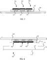
- FIG. 1illustrates a schematic representation of a cross section side view of a tile 100 in a z-axis (not shown in FIG. 1 ) direction showing a direct conversion compound semiconductor layer 101, an integrated circuit (IC) layer 102, and a substrate layer 103 having recesses 104 and sliding electrical contacts 117 according to an embodiment.
- ICintegrated circuit
- the direct conversion compound semiconductor layer 101may also be referred to as a detector semiconductor crystal or a compound semiconductor. It is configured to convert high energy radiation such as x-ray photons into corresponding electronic currents that may be detected.
- the compound semiconductor layer 101is the uppermost layer of the tile 100.
- the compound semiconductor layer 101receives x-ray radiation 118. It should be noted that instead of x-rays, gamma ray radiation may be received.
- the IC layer 102may be an application-specific integrated circuit (ASIC).
- the ASICmay include microprocessors, memory blocks including ROM, RAM, EEPROM, flash memory, analog to digital converters, ADC, and other large building blocks.
- SoCsystem-on-chip
- HDLhardware description language
- VHDLVerilog or VHDL
- FPGAField-programmable gate arrays
- the substrate layer 103The substrate (also referred to as a wafer) may be a solid (usually planar) substance onto which a layer of another substance is applied and to which that second substance adheres.
- the substrate 103may be a slice of material such as ceramics. These serve as the foundation upon which the IC electronic devices such as transistors, diodes, and especially integrated circuits (ICs) are deposited.
- the substrate 103comprises recesses 104 at the lowest corners which are closest to the assembly frame.
- the substrate layer 103may also be referred to as a ceramics substrate.
- a side view of the cross section of the tile 100forms a T-shape, wherein the recesses 104 appear as shoulders.
- the ceramics substrate 103has been tooled to form the T-shape with the shoulders on two opposite sides of the tile 100.
- the recesses 104enable the tile 100 to fit into an assembly frame, as illustrated for example in FIG. 3 .
- the recesses 104enable improvement in thermal conductivity, because material of the substrate layer 103 next to the recesses 104 is configured as a thermal path conducting heat from the tile 100 to the assembly frame.
- the substrate layer 103may comprise thermal conductors, for example copper wires, which may be configured to the shoulder.
- the thermal conductivity from the tile 100is mainly configured via the material next to the recesses 104 to the assembly frame. Heat may be conducted for example from the IC layer 102.
- the width of the recess 104may be 1.3 mm - 1.5 mm, while the total width and the total length of the tile 100 are 10 mm x 10 mm. It should be noted that these are only exemplary measures, and other measures may be used to carve the recesses 104.
- the substrate layer 103comprises sliding electrical contacts 117. They are configured at the bottom of the substrate 103. They contact the assembly frame having elastic forced electrical contacts. Consequently, the tile 100 may be slid when inserted into a recess of the assembly frame. The tile 100 may be slid with a tolerance of +/-100 um. This enables very accurate further positioning of the tile 100 in the array, even after initial placement of the tile in the array.
- the sliding electrical contacts 117may be conductive surfaces having a shape of rectangular, square, flat, semi-oval, semicircular, oval or circular. For example, they may be welded onto the bottom of the tile 100. They connect to a base panel that may be elastically forced into the sliding contacts 117.
- the electronics of the IC layer 102connect to the sliding electrical contacts 117 via the substrate layer 103.
- FIG. 2illustrates a schematic representation of the tile 100 according to an embodiment.
- FIG. 2illustrates a similar tile to the embodiment of FIG. 1 ; however, FIG. 2 illustrates a perspective view of the tile 100.
- the recesses 104are shown to extend along the length of the tile 100 in a y-axis direction (not shown in FIG. 2 ).
- the recesses 104are configured at two opposite sides of the tile 100 and at the lowest corners of these sides.
- the front side and the back sidedo not have the recesses but are substantially flat.
- FIG. 2illustrates the recesses 104 being configured at the two opposite sides, and front and back being flat, the recesses 104 may be configured to all four sides of the tile 100, also including the front side and the back side.
- the compound semiconductor 101, the IC 102 and the substrate 103establish a tile 100.
- One tilehas an array of pixels, and each pixel corresponds to a signal pad on the compound semiconductor in digital imaging in the detector.
- the detectorhas an array (alternatively referred to as a matrix) of tiles 100.
- FIG. 3illustrates a schematic representation of a portion of an array of tiles 100 on an assembly frame 105 according to an embodiment.
- the tile 100is assembled into a recess 106 of the assembly frame 105.
- the recess 106is elongated in the y-axis direction.
- the tile 100may be slid even when it is inserted into the recess 106. This may be possible for x-axis and/or y-axis directions.
- the tile 100may be slid by +/- 100 um in both x-axis and y-axis directions.
- the recess 106is configured to receive the bottom and the recesses 104 of the tile 100 so that the recesses 104 rest on the surface of the assembly frame 105 when the tile 100 is inserted into the recess 106.
- the tile 100may be slid by approximately 100 um within the recess in the x-axis and/or y-axis direction corresponding to the width of the recess 106.
- the recess 106is configured to accommodate the T shape of the tile 100.
- FIG. 4illustrates a schematic representation of an array of tiles 100 on an assembly frame 105 according to an embodiment.
- An embodiment of the array of the tiles 100is shown in FIG. 4 .
- the number of tiles 100 of the array and the shape of the arraymay vary. For example, there may be more or less than nine tiles 100. The shape may also be rectangular, oval or circular, even though a square is shown in FIG. 4 .
- Gaps 119 between the tiles 100are also shown. The gap 119, and consequently a distance between the neighboring tiles 100, may be assembled with a reasonable accuracy. A constant and certain level of distance may be achieved. This may improve the digital imaging and require less digital image correction.
- FIG. 5illustrates a schematic representation of a cross section side view of a detector assembly process illustrating an assembly frame 105 according to an embodiment.
- Recesses 106are manufactured in the assembly frame 105. For example, they may be carved in the frame 105 by a carving tool.
- the detector manufacturing processmay start by making the recesses 106 in the frame 105.
- FIG. 6illustrates a schematic representation of a cross section side view of a detector assembly process illustrating tiles 100 on an assembly frame 105 according to an embodiment.
- the tiles 100are assembled onto the frame 105.
- the base 103 of the tile 100is inserted into the recess 106 of the frame 105.
- the cross sectional T-shape of the tile 100fits into the recess so that the bottom of the tile 100 enters into the recess 106 and the shoulder (the recesses 104 of the tile 100) rests on the upper surface of the frame 105.
- the tile 100may be accurately positioned in x-axis and y-axis directions with respect to the tile array and any neighboring tile 100. Consequently, the gap 119 between the tiles 100 in the tile array may be accurately managed and controlled appropriately.
- the shoulders of the tileare thermally coupled to the frame assembly 105 so that they effectively conduct heat from the tile 100 towards the frame 105.
- FIG. 7illustrates a schematic representation of a cross section side view of a detector assembly process illustrating an interconnection printed circuit board assembly, PCBA, 108 having an assembly frame 105 and tiles 100 attached onto it according to an embodiment.
- the PCBA 108serves as a larger assembly plate assembling the frame 105 into the larger frame assembly.
- FIG. 7shows connectors 107.
- the connectors 107electrically connect the sliding electrical contacts 117 from the tile 100 to the assembly frame 105.
- the connectors 107may be forced to contact the electrical contacts 117, for example the connectors 107 are spring loaded SMD connectors. Consequently, the connectors 107 maintain the connection to the sliding contacts 117, even when there is small variance in the distance between the bottom of the tile 100 and the bottom of the recess 106.
- the connectors 107remain in contact with the sliding connectors 117 even if the tile is slid along the x-axis and the y-axis.
- the end of the connector 107slides on a surface of the sliding connector 117 when the tile 100 is repositioned in the recess 106.
- FIG. 8illustrates a schematic representation of a cross section side view of a detector assembly process illustrating an assembly cover 120 and the PCBA 108 according to an embodiment.
- One end of the assembly frame 105comprises a spring loaded pogo needle 109 which is surrounded by a thermal and electrical insulation frame 110. Another end has the frame 110 without the needle 109.
- the needle 109is attached to the PCBA 108.
- the frame 110is configured between the assembly frame 105 and the PCBA 108.
- the frame 110is configured to thermally and electrically insulate the end of the assembly frame 105 and the tiles 100.
- FIG. 8illustrates only one needle 109, it should be noted that there may be several needles, for example three.
- FIG. 8illustrates an assembly cover 120.
- the cover 120comprises a thermally conductive frame 111 at the ends of the cover 120.
- the thermally conductive frame 111is connected to the PCBA 108 and is attached onto it.
- the cover 120comprises a thermally conductive film 113.
- the film 113is configured under the frame 111 and is thermally connected to it.
- the film 113 and the frame 111effectively conduct heat that is emitted from the tiles 100 into the PCBA 108.
- An electrically conductive film 112is configured on the thermally conductive film 113.
- the electrically conductive film 112may be connected to the direct conversion compound semiconductor 101 and to the pogo needle 109.
- the cover 120comprises a carbon fiber plate 114 protecting the detector and covering the surface of the detector.
- the plate 114 and the films 113, 112may have a relatively small effect on x-ray radiation, and consequently for example the carbon fiber plate 114 may be minimized to a scale of 0.5-1.0 mm (maximum 2 mm). Consequently, the measures and configuration of the plate 114 and the films 113,112 are selected so that the radiation passes through them and enters into the semiconductor layer 101.
- FIG. 9illustrates a schematic representation of a cross section side view of a detector assembly process illustrating a complete assembly 200 according to an embodiment.
- the cover 120has been assembled to the PCBA 108.
- the electrically conductive film 112contacts the tiles 100 and the needle 109.
- the thermal frames 111contact the PCBA 108 and sides of the frames 110.
- FIG. 10illustrates a schematic representation of a top view of an assembly frame 105 showing recesses 106 for receiving tiles 100 according to an embodiment.
- the assembly frame 105comprises elongated recesses 106.
- the embodiment of FIG. 10illustrates three recesses 106, but it should be noted that the number of recesses may vary according to the tile array.
- the recesses 106are parallel.
- the recesses 106are positioned at a certain distance from each other.
- the bottom of the recesses 106contains the connections 107 (not shown in FIG. 10 ).
- the width of the recesses 106is slightly greater than the width of the bottom of the substrate layer 101.
- the length of the recess 106is such that several tiles 100 fit to be assembled in the same recess 106.
- the depth of the recess 106is such that the bottom of the the substrate layer 103, enters into the recess 106 and the shoulder of the recesses 104 contacts the surface of the assembly frame 105
- FIG. 11illustrates a schematic representation of a top view of an assembly frame 105 showing adhesive strips 115 for attaching tiles 100 to the frame 105 according to an embodiment.
- the adhesive strips 115are applied on a surface of the frame 105.
- the strips 115conform to the shape of the recess 106 so that they are elongated and are positioned right next to the recess 106 on the surface of the frame 105. Between the recesses 106 the strips 115 may fill the whole area of the surface. When there is no neighboring recess 106, the strip 115 may fill an area approximately of the size of the area of the strip 115 between two recesses 106.
- the strip 115may also extend beyond both ends of the recesses 106.
- the strip 115may be made of adhesive tape. According to another embodiment, glue may be used instead of the adhesive tape.
- the adhesive strip 115may conduct heat and/or conduct electricity.
- the force of adhesion of the strip 115 for a single tile 100is such that the tile 100 may be detached from the array and the assembly frame 105 without the tile 100 being broken or corrupted.
- the adhesionattaches the tile 100 firmly to the assembly frame 105, yet even a single tile 100 of the whole array may be detached without any of the tiles 100 being broken or corrupted. Consequently, maintenance of the array is easy and cost effective, because the whole array of tiles 100 need not be replaced if a single tile 100 or a few tiles 100 are malfunctioning.
- FIG. 12illustrates a schematic representation of a top view of an assembly frame 105 showing a tile 100 assembled on a recess 106 and attached by adhesive strips 115 according to an embodiment.
- the tiles 100may be assembled one-by-one to the assembly frame 105.
- FIG. 12illustrates the assembly of the first tile 100 that is, by way of demonstration purposes only, positioned at the top and rightmost corner. However, it could be placed in a different location of the array as well.
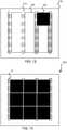
- FIG. 13illustrates a schematic representation of a top view of an assembly frame 105 showing an array of tiles 100 assembled on recesses 106 and attached by adhesive strips 115 according to an embodiment.
- the recesses 106are not illustrated in FIG. 13 , except between two tiles 100 in the y-axis direction.
- the arrayhas 3 * 3 tiles 100, another kind of design may be used as well.
- a rectangular, oval or circular array shapemay be made of the tiles 100, instead of a square as illustrated in FIG. 13 .
- FIG. 14illustrates a schematic representation of a cross section of a detector 200 having an array of tiles 100 according to an embodiment.
- X-ray radiation 118is emitted from a source (not shown in FIG. 14 ).
- An object 300 to be detected and inspected by the x-ray radiation 118is shown between the radiation source and the detector 200.
- the detector 200comprises an array having nine tiles 100 - 100_8 in the cross section of the detector 200, for example in the x-axis direction.
- FIG. 14illustrates the detection devices 200 comprising tiles 100 having a T-shape cross section.
- the tiles 100are slidingly assembled into the recesses 106 of the assembly frame 105.
- the assembly frame 105has adhesive strips 115 to attach the tiles 100 to the frame 105 according to the embodiments.
- the device 200may be a part of an imaging system for detecting the object 300, comprising the tiles 100 as described in any of these embodiments.
- the systemmay be applied for example in medical imaging, security imaging and/or industrial imaging.
- An embodimentrelates to a device, comprising: a direct conversion compound semiconductor layer configured to convert x-ray photons into an electric current; an integrated circuit, IC, layer situated next to the direct conversion compound semiconductor layer and configured to receive the electric current and process the electric current; and a substrate layer situated next to the IC layer configured to conduct heat emitted from the IC layer; wherein the substrate layer comprises recesses at corners of a cross section of the substrate; and wherein the substrate layer further comprises sliding electrical contacts between the corners, wherein the sliding electrical contacts are connected to the IC layer through the substrate layer to receive the processed electric current.
- the recessesare configured to the lowest corners of the cross section of the substrate.
- the recessesare configured to establish a T-shape for a cross section of the device having the direct conversion compound semiconductor layer, the IC layer and the substrate layer.
- material of the substrate layer next to the recessescomprises thermally conductive material.
- further including an assembly framewherein the assembly frame comprises recesses, each recess configured to receive a lowest part of the substrate layer being at a same level as the recesses, and an upper part of the substrate, which is above the recesses, rests on a surface of the assembly frame.
- the assembly framefurther includes elastic force loaded electrical connections at a bottom of the recesses, wherein the elastic force loaded electrical connections are configured to make contact with the sliding electrical contacts when the lowest part of the substrate enters the recess of the assembly frame and the upper part of the substrate rests on the surface of the assembly frame.
- the contact between the sliding electric contacts of the substrate layer and the elastic force loaded electrical connectionscan be maintained when the device is slid in x-axis and y-axis directions.
- the assembly framefurther includes elongated adhesive strips on a top surface of the frame next to the recesses.
- the direct conversion compound semiconductor layercomprises cadmium telluride or cadmium zinc telluride.
- the devicecomprises a tile.
- the tilecan be slid so as to position the tile with respect to at least one neighboring tile.
- a detectorcomprising an array of tiles according to above.
- an imaging systemcomprises: an x-ray source; the detector according to above.
Landscapes
- Physics & Mathematics (AREA)
- Health & Medical Sciences (AREA)
- Life Sciences & Earth Sciences (AREA)
- General Physics & Mathematics (AREA)
- High Energy & Nuclear Physics (AREA)
- Molecular Biology (AREA)
- Spectroscopy & Molecular Physics (AREA)
- Measurement Of Radiation (AREA)
- Solid State Image Pick-Up Elements (AREA)
- Light Receiving Elements (AREA)
- Apparatus For Radiation Diagnosis (AREA)
Abstract
Description
- Direct conversion compound semiconductor based detectors and detector arrays are utilized in radiation imaging in order to convert high energy radiation for example x-ray photons directly into electric charges. They are typically comprised of an x-ray photoconductor layer grown directly on top of a charge collector and a readout layer (such as room temperature semiconductors). The detectors are commonly utilized in arrays of multiple tiles such that an increased image size with improved resolution may be generated. Another reason for using the array with tiles, each tile having a relatively small size, is high costs of the direct conversion compound semiconductors.
- The performance of the detectors can be important to many imaging applications. Linearity, uniformity, stability, and consistency may be relevant for peripheral tiles. For many applications, the imaging requirements can be very stringent. Vertical stacking of the tiles having a direct conversion compound semiconductor layer, an integrated circuit, IC, layer and a substrate layer may present some problematic conditions. For example, the heat generated by the IC can couple to the detector and introduce unwanted noise and thermal variation. Further, an array of the tiles requires very accurate and precise positioning with respect to the tiles. A tile should be carefully positioned to a right position in the array, especially with respect to the neighboring tiles. Furthermore, the detector made of the array needs to be maintained, for example in case of malfunction.
- This summary is provided to introduce a selection of concepts in a simplified form that are further described below in the detailed description. This summary is not intended to identify key features or essential features of the claimed subject matter, nor is it intended to be used to limit the scope of the claimed subject matter.
- It is an object to provide a direct conversion compound semiconductor tile structure. The object is achieved by the features of the independent claims. Some embodiments are described in the dependent claims. According to an embodiment, a device comprises: a direct conversion compound semiconductor layer configured to convert high energy radiation photons into an electric current; an integrated circuit, IC, layer situated next to the direct conversion compound semiconductor layer and configured to receive the electric current and process the electric current; and a substrate layer situated next to the IC layer configured to conduct heat emitted from the IC layer; wherein the substrate layer comprises recesses at corners of a cross section of the substrate; and wherein the substrate layer further comprises sliding electrical contacts between the corners, wherein the sliding electrical contacts are connected to the IC layer through the substrate layer to receive the processed electric current.
- Other embodiments relate to a detector comprising an array of tiles according to the device, and an imaging system comprising: an x-ray source and the detector.
- Many of the attendant features will be more readily appreciated as they become better understood by reference to the following detailed description considered in connection with the accompanying drawings.
- The present description will be better understood from the following detailed description read in light of the accompanying drawings, wherein:
FIG. 1 illustrates a schematic representation of a cross section side view of a tile showing a direct conversion compound semiconductor layer, an integrated circuit layer, and a substrate layer having shoulders and sliding contacts according to an embodiment;FIG. 2 illustrates a schematic representation of the tile according to an embodiment;FIG. 3 illustrates a schematic representation of a portion of an array of tiles on an assembly frame according to an embodiment;FIG. 4 illustrates a schematic representation of an array of tiles on an assembly frame according to an embodiment;FIG. 5 illustrates a schematic representation of a cross section side view of a detector assembly process illustrating an assembly frame according to an embodiment;FIG. 6 illustrates a schematic representation of a cross section side view of a detector assembly process illustrating tiles on an assembly frame according to an embodiment;FIG. 7 illustrates a schematic representation of a cross section side view of a detector assembly process illustrating an interconnection printed circuit board assembly, PCBA, having an assembly frame and tiles attached to it according to an embodiment;FIG. 8 illustrates a schematic representation of a cross section side view of a detector assembly process illustrating a cover and the PCBA according to an embodiment;FIG. 9 illustrates a schematic representation of a cross section side view of a detector assembly process illustrating a complete detector assembly according to an embodiment;FIG. 10 illustrates a schematic representation of a top view of an assembly frame showing a recess for receiving tiles according to an embodiment;FIG. 11 illustrates a schematic representation of a top view of an assembly frame showing adhesive strips for attaching tiles to an assembly frame according to an embodiment;FIG. 12 illustrates a schematic representation of a top view of an assembly frame showing a tile assembled on a recess and attached by adhesive strips according to an embodiment;FIG. 13 illustrates a schematic representation of a top view of an assembly frame showing an array of tiles assembled on a recess and attached by adhesive strips according to an embodiment; andFIG. 14 illustrates a schematic representation of a cross section of a detector having the tiles according to an embodiment.- Like references are used to designate like parts in the accompanying drawings.
- The detailed description provided below in connection with the appended drawings is intended as a description of the embodiments and is not intended to represent the only forms in which the embodiment may be constructed or utilized. However, the same or equivalent functions and structures may be accomplished by different embodiments.
- According to an embodiment, layers of a direct conversion compound semiconductor, an integrated circuit (IC) and a substrate establish a tile. An x-ray detector has an array of tiles. The substrate of the tile has recesses at the corners closest to an assembly frame, onto which the tile is attached. Consequently, a cross section side view of the tile forms a T-shape having shoulders as the recess. The shoulders allow a thermal path from the tile to the assembly frame onto which the tiles are assembled. Furthermore, the bottom surface of the substrate comprises sliding electric contact points. When assembling the array, a tile may be accurately slid to an appropriate location on the assembly frame, and electrical contact between the tile and recesses of the assembly frame can be maintained during sliding. The recesses of the assembly frame accommodate the tile so that the bottom part of the tile enters into the recess of the assembly frame and shoulders of the tile rest on the upper surface of the assembly frame.
- The ceramic substrate of the tile has been configured to have contact with the assembly frame. It also allows electrical contact from the tile to read-out electronics of the assembly frame. From a side view, the ceramic substrate forms a T-shape. The shoulder of the T-shape allows the thermal path from the tile to the thermally controlled cooling plate below the assembly frame.
- A single tile is attached to the assembly frame by using glue with a low adhesion force. Alternatively, the used glue may be thermally softened, for example if a tile needs to be replaced. A dual sided low adhesion tape may also be used instead of the glue. The adhesive force is low so that a single tile can be detached from the array later, for example for maintenance purposes
- The embodiment enables maintainability and re-work of the detector array, for example in a case of a single or multiple tile malfunctions. An individual tile which malfunctions can be replaced without compromising the complete array functionality. Typical automatically die bonded arrays cannot be reworked easily or at all, causing expensive scrap on the full detector array assembly.
- The sliding electrical contact at the assembly stage enables high accuracy for positioning each tile with respect to each other in the array. For example, a tolerance of +/- 5 micrometers (um) may be achieved for positioning the tile in the array. Tiles may be assembled against a nominal distance of 20 um with respect to each other's edges. Furthermore, shoulders of the tile enable the tile to fit in the assembly frame. They are also configured as a thermal path transferring heat away from the tile to the assembly frame. Consequently, thermal management of the detector plane may be improved. Furthermore, a distance between electronics of the tile and read-out electronics of the printed circuit board assembly onto which the assembly frame is attached is short, thus minimizing electrical noise.
- An industrial scale assembly of detector arrays may be manufactured, and the detector array may be designed and manufactured modularly. The assembly tolerance of a tile in the array and thermal management of the tile may be improved.
- Although the embodiments may be described and illustrated herein as being implemented in a direct conversion compound semiconductor, this is only an example implementation and not a limitation. As those skilled in the art will appreciate, the present embodiments are suitable for application in a variety of different types of detector semiconductor crystals such as Cadmium Telluride (CdTe), Cadmium Zinc Telluride CdZnTe, etc.
FIG. 1 illustrates a schematic representation of a cross section side view of atile 100 in a z-axis (not shown inFIG. 1 ) direction showing a direct conversioncompound semiconductor layer 101, an integrated circuit (IC)layer 102, and asubstrate layer 103 havingrecesses 104 and sliding electrical contacts 117 according to an embodiment.- The direct conversion
compound semiconductor layer 101 may also be referred to as a detector semiconductor crystal or a compound semiconductor. It is configured to convert high energy radiation such as x-ray photons into corresponding electronic currents that may be detected. Thecompound semiconductor layer 101 is the uppermost layer of thetile 100. Thecompound semiconductor layer 101 receivesx-ray radiation 118. It should be noted that instead of x-rays, gamma ray radiation may be received. Under thecompound semiconductor layer 101 there is theIC layer 102. TheIC layer 102 may be an application-specific integrated circuit (ASIC). The ASIC may include microprocessors, memory blocks including ROM, RAM, EEPROM, flash memory, analog to digital converters, ADC, and other large building blocks. This kind of ASIC is often termed a SoC (system-on-chip). It may be configured using a hardware description language (HDL), such as Verilog or VHDL, to describe the functionality of ASICs. Instead of an ASIC, Field-programmable gate arrays (FPGA) may be used as programmable logic blocks and programmable interconnects allowing the same FPGA to be used in many different applications. The lowermost layer is thesubstrate layer 103. The substrate (also referred to as a wafer) may be a solid (usually planar) substance onto which a layer of another substance is applied and to which that second substance adheres. Thesubstrate 103 may be a slice of material such as ceramics. These serve as the foundation upon which the IC electronic devices such as transistors, diodes, and especially integrated circuits (ICs) are deposited. - The
substrate 103 comprisesrecesses 104 at the lowest corners which are closest to the assembly frame. Thesubstrate layer 103 may also be referred to as a ceramics substrate. A side view of the cross section of thetile 100 forms a T-shape, wherein therecesses 104 appear as shoulders. Theceramics substrate 103 has been tooled to form the T-shape with the shoulders on two opposite sides of thetile 100. Therecesses 104 enable thetile 100 to fit into an assembly frame, as illustrated for example inFIG. 3 . Therecesses 104 enable improvement in thermal conductivity, because material of thesubstrate layer 103 next to therecesses 104 is configured as a thermal path conducting heat from thetile 100 to the assembly frame. According to an embodiment, thesubstrate layer 103 may comprise thermal conductors, for example copper wires, which may be configured to the shoulder. The thermal conductivity from thetile 100 is mainly configured via the material next to therecesses 104 to the assembly frame. Heat may be conducted for example from theIC layer 102. The width of therecess 104 may be 1.3 mm - 1.5 mm, while the total width and the total length of thetile 100 are 10 mm x 10 mm. It should be noted that these are only exemplary measures, and other measures may be used to carve therecesses 104. - The
substrate layer 103 comprises sliding electrical contacts 117. They are configured at the bottom of thesubstrate 103. They contact the assembly frame having elastic forced electrical contacts. Consequently, thetile 100 may be slid when inserted into a recess of the assembly frame. Thetile 100 may be slid with a tolerance of +/-100 um. This enables very accurate further positioning of thetile 100 in the array, even after initial placement of the tile in the array. The sliding electrical contacts 117 may be conductive surfaces having a shape of rectangular, square, flat, semi-oval, semicircular, oval or circular. For example, they may be welded onto the bottom of thetile 100. They connect to a base panel that may be elastically forced into the sliding contacts 117. The electronics of theIC layer 102 connect to the sliding electrical contacts 117 via thesubstrate layer 103. FIG. 2 illustrates a schematic representation of thetile 100 according to an embodiment.FIG. 2 illustrates a similar tile to the embodiment ofFIG. 1 ; however,FIG. 2 illustrates a perspective view of thetile 100. Therecesses 104 are shown to extend along the length of thetile 100 in a y-axis direction (not shown inFIG. 2 ). Therecesses 104 are configured at two opposite sides of thetile 100 and at the lowest corners of these sides. The front side and the back side do not have the recesses but are substantially flat. Although,FIG. 2 illustrates therecesses 104 being configured at the two opposite sides, and front and back being flat, therecesses 104 may be configured to all four sides of thetile 100, also including the front side and the back side.- The
compound semiconductor 101, theIC 102 and thesubstrate 103 establish atile 100. One tile has an array of pixels, and each pixel corresponds to a signal pad on the compound semiconductor in digital imaging in the detector. The detector has an array (alternatively referred to as a matrix) oftiles 100. FIG. 3 illustrates a schematic representation of a portion of an array oftiles 100 on anassembly frame 105 according to an embodiment. Thetile 100 is assembled into arecess 106 of theassembly frame 105. Therecess 106 is elongated in the y-axis direction. Thetile 100 may be slid even when it is inserted into therecess 106. This may be possible for x-axis and/or y-axis directions. According to an embodiment, thetile 100 may be slid by +/- 100 um in both x-axis and y-axis directions. Therecess 106 is configured to receive the bottom and therecesses 104 of thetile 100 so that therecesses 104 rest on the surface of theassembly frame 105 when thetile 100 is inserted into therecess 106. Thetile 100 may be slid by approximately 100 um within the recess in the x-axis and/or y-axis direction corresponding to the width of therecess 106. Therecess 106 is configured to accommodate the T shape of thetile 100.FIG. 4 illustrates a schematic representation of an array oftiles 100 on anassembly frame 105 according to an embodiment. An embodiment of the array of thetiles 100 is shown inFIG. 4 . It should be noted that the number oftiles 100 of the array and the shape of the array may vary. For example, there may be more or less than ninetiles 100. The shape may also be rectangular, oval or circular, even though a square is shown inFIG. 4 .Gaps 119 between thetiles 100 are also shown. Thegap 119, and consequently a distance between the neighboringtiles 100, may be assembled with a reasonable accuracy. A constant and certain level of distance may be achieved. This may improve the digital imaging and require less digital image correction.FIG. 5 illustrates a schematic representation of a cross section side view of a detector assembly process illustrating anassembly frame 105 according to an embodiment.Recesses 106 are manufactured in theassembly frame 105. For example, they may be carved in theframe 105 by a carving tool. The detector manufacturing process may start by making therecesses 106 in theframe 105.FIG. 6 illustrates a schematic representation of a cross section side view of a detector assemblyprocess illustrating tiles 100 on anassembly frame 105 according to an embodiment. Thetiles 100 are assembled onto theframe 105. Thebase 103 of thetile 100 is inserted into therecess 106 of theframe 105. The cross sectional T-shape of thetile 100 fits into the recess so that the bottom of thetile 100 enters into therecess 106 and the shoulder (therecesses 104 of the tile 100) rests on the upper surface of theframe 105. When inserted, thetile 100 may be accurately positioned in x-axis and y-axis directions with respect to the tile array and any neighboringtile 100. Consequently, thegap 119 between thetiles 100 in the tile array may be accurately managed and controlled appropriately. Furthermore, the shoulders of the tile are thermally coupled to theframe assembly 105 so that they effectively conduct heat from thetile 100 towards theframe 105.FIG. 7 illustrates a schematic representation of a cross section side view of a detector assembly process illustrating an interconnection printed circuit board assembly, PCBA, 108 having anassembly frame 105 andtiles 100 attached onto it according to an embodiment. ThePCBA 108 serves as a larger assembly plate assembling theframe 105 into the larger frame assembly. Furthermore,FIG. 7 showsconnectors 107. Theconnectors 107 electrically connect the sliding electrical contacts 117 from thetile 100 to theassembly frame 105. Theconnectors 107 may be forced to contact the electrical contacts 117, for example theconnectors 107 are spring loaded SMD connectors. Consequently, theconnectors 107 maintain the connection to the sliding contacts 117, even when there is small variance in the distance between the bottom of thetile 100 and the bottom of therecess 106. Furthermore, theconnectors 107 remain in contact with the sliding connectors 117 even if the tile is slid along the x-axis and the y-axis. The end of theconnector 107 slides on a surface of the sliding connector 117 when thetile 100 is repositioned in therecess 106.FIG. 8 illustrates a schematic representation of a cross section side view of a detector assembly process illustrating anassembly cover 120 and thePCBA 108 according to an embodiment. One end of theassembly frame 105 comprises a spring loadedpogo needle 109 which is surrounded by a thermal andelectrical insulation frame 110. Another end has theframe 110 without theneedle 109. Theneedle 109 is attached to thePCBA 108. Theframe 110 is configured between theassembly frame 105 and thePCBA 108. Theframe 110 is configured to thermally and electrically insulate the end of theassembly frame 105 and thetiles 100. AlthoughFIG. 8 illustrates only oneneedle 109, it should be noted that there may be several needles, for example three.FIG. 8 illustrates anassembly cover 120. It comprises a thermallyconductive frame 111 at the ends of thecover 120. When thecover 120 is assembled, as shown inFIG. 9 , the thermallyconductive frame 111 is connected to thePCBA 108 and is attached onto it. Thecover 120 comprises a thermallyconductive film 113. Thefilm 113 is configured under theframe 111 and is thermally connected to it. Thefilm 113 and theframe 111 effectively conduct heat that is emitted from thetiles 100 into thePCBA 108. An electricallyconductive film 112 is configured on the thermallyconductive film 113. The electricallyconductive film 112 may be connected to the directconversion compound semiconductor 101 and to thepogo needle 109. Thecover 120 comprises acarbon fiber plate 114 protecting the detector and covering the surface of the detector. Theplate 114 and thefilms carbon fiber plate 114 may be minimized to a scale of 0.5-1.0 mm (maximum 2 mm). Consequently, the measures and configuration of theplate 114 and the films 113,112 are selected so that the radiation passes through them and enters into thesemiconductor layer 101.FIG. 9 illustrates a schematic representation of a cross section side view of a detector assembly process illustrating acomplete assembly 200 according to an embodiment. Thecover 120 has been assembled to thePCBA 108. The electricallyconductive film 112 contacts thetiles 100 and theneedle 109. Furthermore, thethermal frames 111 contact thePCBA 108 and sides of theframes 110.FIG. 10 illustrates a schematic representation of a top view of anassembly frame 105 showingrecesses 106 for receivingtiles 100 according to an embodiment. Theassembly frame 105 comprises elongated recesses 106. The embodiment ofFIG. 10 illustrates threerecesses 106, but it should be noted that the number of recesses may vary according to the tile array. Therecesses 106 are parallel. Therecesses 106 are positioned at a certain distance from each other. The bottom of therecesses 106 contains the connections 107 (not shown inFIG. 10 ). The width of therecesses 106 is slightly greater than the width of the bottom of thesubstrate layer 101. The length of therecess 106 is such thatseveral tiles 100 fit to be assembled in thesame recess 106. The depth of therecess 106 is such that the bottom of the thesubstrate layer 103, enters into therecess 106 and the shoulder of therecesses 104 contacts the surface of theassembly frame 105.FIG. 11 illustrates a schematic representation of a top view of anassembly frame 105 showingadhesive strips 115 for attachingtiles 100 to theframe 105 according to an embodiment. Theadhesive strips 115 are applied on a surface of theframe 105. Thestrips 115 conform to the shape of therecess 106 so that they are elongated and are positioned right next to therecess 106 on the surface of theframe 105. Between therecesses 106 thestrips 115 may fill the whole area of the surface. When there is no neighboringrecess 106, thestrip 115 may fill an area approximately of the size of the area of thestrip 115 between tworecesses 106. Thestrip 115 may also extend beyond both ends of therecesses 106. According to an embodiment, thestrip 115 may be made of adhesive tape. According to another embodiment, glue may be used instead of the adhesive tape. Theadhesive strip 115 may conduct heat and/or conduct electricity. The force of adhesion of thestrip 115 for asingle tile 100 is such that thetile 100 may be detached from the array and theassembly frame 105 without thetile 100 being broken or corrupted. The adhesion attaches thetile 100 firmly to theassembly frame 105, yet even asingle tile 100 of the whole array may be detached without any of thetiles 100 being broken or corrupted. Consequently, maintenance of the array is easy and cost effective, because the whole array oftiles 100 need not be replaced if asingle tile 100 or afew tiles 100 are malfunctioning.FIG. 12 illustrates a schematic representation of a top view of anassembly frame 105 showing atile 100 assembled on arecess 106 and attached byadhesive strips 115 according to an embodiment. Thetiles 100 may be assembled one-by-one to theassembly frame 105.FIG. 12 illustrates the assembly of thefirst tile 100 that is, by way of demonstration purposes only, positioned at the top and rightmost corner. However, it could be placed in a different location of the array as well.FIG. 13 illustrates a schematic representation of a top view of anassembly frame 105 showing an array oftiles 100 assembled onrecesses 106 and attached byadhesive strips 115 according to an embodiment. Therecesses 106 are not illustrated inFIG. 13 , except between twotiles 100 in the y-axis direction. Although the array has 3 * 3tiles 100, another kind of design may be used as well. For example, a rectangular, oval or circular array shape may be made of thetiles 100, instead of a square as illustrated inFIG. 13 .FIG. 14 illustrates a schematic representation of a cross section of adetector 200 having an array oftiles 100 according to an embodiment.X-ray radiation 118 is emitted from a source (not shown inFIG. 14 ). Anobject 300 to be detected and inspected by thex-ray radiation 118 is shown between the radiation source and thedetector 200. Thedetector 200 comprises an array having nine tiles 100 - 100_8 in the cross section of thedetector 200, for example in the x-axis direction.FIG. 14 illustrates thedetection devices 200 comprisingtiles 100 having a T-shape cross section. Thetiles 100 are slidingly assembled into therecesses 106 of theassembly frame 105. Theassembly frame 105 hasadhesive strips 115 to attach thetiles 100 to theframe 105 according to the embodiments. Thedevice 200 may be a part of an imaging system for detecting theobject 300, comprising thetiles 100 as described in any of these embodiments. The system may be applied for example in medical imaging, security imaging and/or industrial imaging.- Any range or device value given herein may be extended or altered without losing the effect sought. Also any embodiment may be combined with another embodiment unless explicitly disallowed.
- Although the subject matter has been described in language specific to structural features and/or acts, it is to be understood that the subject matter defined in the appended claims is not necessarily limited to the specific features or acts described above. Rather, the specific features and acts described above are disclosed as examples of implementing the claims and other equivalent features and acts are intended to be within the scope of the claims.
- An embodiment relates to a device, comprising: a direct conversion compound semiconductor layer configured to convert x-ray photons into an electric current; an integrated circuit, IC, layer situated next to the direct conversion compound semiconductor layer and configured to receive the electric current and process the electric current; and a substrate layer situated next to the IC layer configured to conduct heat emitted from the IC layer; wherein the substrate layer comprises recesses at corners of a cross section of the substrate; and wherein the substrate layer further comprises sliding electrical contacts between the corners, wherein the sliding electrical contacts are connected to the IC layer through the substrate layer to receive the processed electric current.
- Alternatively or in addition to the above, the recesses are configured to the lowest corners of the cross section of the substrate. Alternatively or in addition to the above, the recesses are configured to establish a T-shape for a cross section of the device having the direct conversion compound semiconductor layer, the IC layer and the substrate layer. Alternatively or in addition to the above, material of the substrate layer next to the recesses comprises thermally conductive material. Alternatively or in addition to the above, further including an assembly frame, wherein the assembly frame comprises recesses, each recess configured to receive a lowest part of the substrate layer being at a same level as the recesses, and an upper part of the substrate, which is above the recesses, rests on a surface of the assembly frame. Alternatively or in addition to the above, the assembly frame further includes elastic force loaded electrical connections at a bottom of the recesses, wherein the elastic force loaded electrical connections are configured to make contact with the sliding electrical contacts when the lowest part of the substrate enters the recess of the assembly frame and the upper part of the substrate rests on the surface of the assembly frame. Alternatively or in addition to the above, the contact between the sliding electric contacts of the substrate layer and the elastic force loaded electrical connections can be maintained when the device is slid in x-axis and y-axis directions. Alternatively or in addition to the above, the assembly frame further includes elongated adhesive strips on a top surface of the frame next to the recesses. Alternatively or in addition to the above, surfaces of the recesses of the substrate layer which rest on the adhesive strips adhere to the adhesive strips. Alternatively or in addition to the above, an adhesion force of the adhesive strip is low so that the substrate layer can be detached without any layers and the assembly frame being corrupted. Alternatively or in addition to the above, the direct conversion compound semiconductor layer comprises cadmium telluride or cadmium zinc telluride.
- According to an embodiment, the device comprises a tile. Alternatively or in addition to the above, the tile can be slid so as to position the tile with respect to at least one neighboring tile.
- According to an embodiment, a detector comprising an array of tiles according to above. According to another embodiment, an imaging system comprises: an x-ray source; the detector according to above.
- It will be understood that the benefits and advantages described above may relate to one embodiment or may relate to several embodiments. The embodiments are not limited to those that solve any or all of the stated problems or those that have any or all of the stated benefits and advantages. It will further be understood that reference to 'an' item refers to one or more of those items.
- The steps of the methods described herein may be carried out in any suitable order, or simultaneously where appropriate. Additionally, individual blocks may be deleted from any of the methods without departing from the spirit and scope of the subject matter described herein. Aspects of any of the examples described above may be combined with aspects of any of the other examples described to form further examples without losing the effect sought.
- The term 'comprising' is used herein to mean including the method, blocks or elements identified, but that such blocks or elements do not comprise an exclusive list and a method or apparatus may contain additional blocks or elements.
- It will be understood that the above description is given by way of example only and that various modifications may be made by those skilled in the art. The above specification, examples and data provide a complete description of the structure and use of exemplary embodiments. Although various embodiments have been described above with a certain degree of particularity, or with reference to one or more individual embodiments, those skilled in the art could make numerous alterations to the disclosed embodiments without departing from the spirit or scope of this specification.
Claims (15)
- A device, comprising:a direct conversion compound semiconductor layer configured to convert high energy radiation photons into an electric current;an integrated circuit, IC, layer situated next to the direct conversion compound semiconductor layer and configured to receive the electric current and process the electric current; anda substrate layer situated next to the IC layer configured to conduct heat emitted from the IC layer;wherein the substrate layer comprises recesses at corners of a cross section of the substrate; andwherein the substrate layer further comprises sliding electrical contacts between the corners, wherein the sliding electrical contacts are connected to the IC layer through the substrate layer to receive the processed electric current.
- The device of claim 1, wherein the recesses are configured to the lowest corners of the cross section of the substrate.
- The device of any preceding claim, wherein the recesses are configured to establish a T-shape for a cross section of the device having the direct conversion compound semiconductor layer, the IC layer and the substrate layer.
- The device of any preceding claim, wherein material of the substrate layer next to the recesses comprises thermally conductive material.
- The device of any preceding claim, further including an assembly frame, wherein the assembly frame comprises recesses, each recess configured to receive a lowest part of the substrate layer being at a same level as the recesses, and an upper part of the substrate, which is above the recesses, rests on a surface of the assembly frame.
- The device of any preceding claim, wherein the assembly frame further includes elastic force loaded electrical connections at a bottom of the recesses, wherein the elastic force loaded electrical connections are configured to make contact with the sliding electrical contacts when the lowest part of the substrate enters the recess of the assembly frame and the upper part of the substrate rests on the surface of the assembly frame.
- The device of any preceding claim, wherein the contact between the sliding electric contacts of the substrate layer and the elastic force loaded electrical connections can be maintained when the device is slid in x-axis and y-axis directions.
- The device of any preceding claim, wherein the assembly frame further includes elongated adhesive strips on a top surface of the frame next to the recesses.
- The device of any preceding claim, wherein surfaces of the recesses of the substrate layer which rest on the adhesive strips adhere to the adhesive strips.
- The device of any preceding claim, wherein an adhesion force of the adhesive strip is low so that the substrate layer can be detached without any layers and the assembly frame being corrupted.
- The device of any preceding claim, wherein the direct conversion compound semiconductor layer comprises cadmium telluride or cadmium zinc telluride.
- The device of any preceding claim, wherein the device comprises a tile.
- The device of any preceding claim, wherein the tile can be slid so as to position the tile with respect to at least one neighboring tile.
- A detector comprising an array of tiles according to any preceding claim.
- An imaging system, comprising:a high energy radiation source;the detector according to any preceding claim.
Priority Applications (5)
| Application Number | Priority Date | Filing Date | Title |
|---|---|---|---|
| EP17153478.7AEP3355081B1 (en) | 2017-01-27 | 2017-01-27 | Direct conversion compound semiconductor tile structure |
| US16/480,125US20190391281A1 (en) | 2017-01-27 | 2018-01-25 | Direct conversion compound semiconductor title structure |
| PCT/EP2018/051768WO2018138177A1 (en) | 2017-01-27 | 2018-01-25 | Direct conversion compound semiconductor tile structure |
| JP2019534961AJP7071983B2 (en) | 2017-01-27 | 2018-01-25 | Direct conversion compound semiconductor tile structure |
| CN201880008982.5ACN110291424B (en) | 2017-01-27 | 2018-01-25 | Direct conversion compound semiconductor slice structure |
Applications Claiming Priority (1)
| Application Number | Priority Date | Filing Date | Title |
|---|---|---|---|
| EP17153478.7AEP3355081B1 (en) | 2017-01-27 | 2017-01-27 | Direct conversion compound semiconductor tile structure |
Publications (2)
| Publication Number | Publication Date |
|---|---|
| EP3355081A1true EP3355081A1 (en) | 2018-08-01 |
| EP3355081B1 EP3355081B1 (en) | 2019-06-19 |
Family
ID=57963011
Family Applications (1)
| Application Number | Title | Priority Date | Filing Date |
|---|---|---|---|
| EP17153478.7AActiveEP3355081B1 (en) | 2017-01-27 | 2017-01-27 | Direct conversion compound semiconductor tile structure |
Country Status (5)
| Country | Link |
|---|---|
| US (1) | US20190391281A1 (en) |
| EP (1) | EP3355081B1 (en) |
| JP (1) | JP7071983B2 (en) |
| CN (1) | CN110291424B (en) |
| WO (1) | WO2018138177A1 (en) |
Citations (4)
| Publication number | Priority date | Publication date | Assignee | Title |
|---|---|---|---|---|
| US5635718A (en)* | 1996-01-16 | 1997-06-03 | Minnesota Mining And Manufacturing Company | Multi-module radiation detecting device and fabrication method |
| US20050139757A1 (en)* | 2003-12-30 | 2005-06-30 | Iwanczyk Jan S. | Pixelated cadmium zinc telluride based photon counting mode detector |
| US20070111567A1 (en)* | 2003-11-03 | 2007-05-17 | Commissariat A L'energie Atomique | Method and device for connecting chips |
| WO2015012866A1 (en)* | 2013-07-26 | 2015-01-29 | Analogic Corporation | Detector unit for detector array of radiation imaging modality |
Family Cites Families (13)
| Publication number | Priority date | Publication date | Assignee | Title |
|---|---|---|---|---|
| EP0784801B1 (en)* | 1994-09-29 | 2002-04-24 | DIRECT (Digital Imaging Readout) | A radiation detection system and processes for preparing the same |
| EP1381408A4 (en)* | 2001-02-22 | 2007-06-13 | Insulet Corp | Modular infusion device and method |
| US6510195B1 (en)* | 2001-07-18 | 2003-01-21 | Koninklijke Philips Electronics, N.V. | Solid state x-radiation detector modules and mosaics thereof, and an imaging method and apparatus employing the same |
| JP5098126B2 (en)* | 2001-08-07 | 2012-12-12 | 株式会社ニコン | X-ray generator, exposure apparatus, exposure method, and device manufacturing method |
| KR101975741B1 (en)* | 2009-11-13 | 2019-05-09 | 가부시키가이샤 한도오따이 에네루기 켄큐쇼 | Method for packaging target material and method for mounting target |
| WO2013012809A1 (en)* | 2011-07-15 | 2013-01-24 | Brookhaven Science Associates, Llc | Radiation detector modules based on multi-layer cross strip semiconductor detectors |
| JP6081697B2 (en)* | 2011-12-07 | 2017-02-15 | 浜松ホトニクス株式会社 | Sensor unit and solid-state imaging device |
| WO2013112435A1 (en)* | 2012-01-24 | 2013-08-01 | Cooledge Lighting Inc. | Light - emitting devices having discrete phosphor chips and fabrication methods |
| JP5600722B2 (en)* | 2012-11-02 | 2014-10-01 | 株式会社堀場製作所 | Radiation detector, radiation detection apparatus, and X-ray analysis apparatus |
| DE102014221829B4 (en)* | 2014-10-27 | 2018-02-22 | Siemens Healthcare Gmbh | Method for producing a sensor board for a detector module and detector module produced thereby |
| DE102014225396B3 (en)* | 2014-12-10 | 2016-04-28 | Siemens Aktiengesellschaft | Sensor board for a detector module and method for its production |
| US10217790B2 (en)* | 2015-01-15 | 2019-02-26 | Koninklijke Philips N.V. | Imaging detector module assembly |
| US20160291269A1 (en)* | 2015-04-01 | 2016-10-06 | Coriant Advanced Technology, LLC | Photonic integrated circuit chip packaging |
- 2017
- 2017-01-27EPEP17153478.7Apatent/EP3355081B1/enactiveActive
- 2018
- 2018-01-25WOPCT/EP2018/051768patent/WO2018138177A1/ennot_activeCeased
- 2018-01-25JPJP2019534961Apatent/JP7071983B2/enactiveActive
- 2018-01-25USUS16/480,125patent/US20190391281A1/ennot_activeAbandoned
- 2018-01-25CNCN201880008982.5Apatent/CN110291424B/enactiveActive
Patent Citations (4)
| Publication number | Priority date | Publication date | Assignee | Title |
|---|---|---|---|---|
| US5635718A (en)* | 1996-01-16 | 1997-06-03 | Minnesota Mining And Manufacturing Company | Multi-module radiation detecting device and fabrication method |
| US20070111567A1 (en)* | 2003-11-03 | 2007-05-17 | Commissariat A L'energie Atomique | Method and device for connecting chips |
| US20050139757A1 (en)* | 2003-12-30 | 2005-06-30 | Iwanczyk Jan S. | Pixelated cadmium zinc telluride based photon counting mode detector |
| WO2015012866A1 (en)* | 2013-07-26 | 2015-01-29 | Analogic Corporation | Detector unit for detector array of radiation imaging modality |
Also Published As
| Publication number | Publication date |
|---|---|
| JP7071983B2 (en) | 2022-05-19 |
| WO2018138177A1 (en) | 2018-08-02 |
| CN110291424B (en) | 2023-06-30 |
| US20190391281A1 (en) | 2019-12-26 |
| EP3355081B1 (en) | 2019-06-19 |
| CN110291424A (en) | 2019-09-27 |
| JP2020506375A (en) | 2020-02-27 |
Similar Documents
| Publication | Publication Date | Title |
|---|---|---|
| US7339176B2 (en) | Radiation detector head | |
| JP6209532B2 (en) | Attaching tiles for PET detectors | |
| US8850697B2 (en) | Method for manufacturing a radiation imaging panel comprising imaging tiles | |
| RU2013147397A (en) | SPECTRAL IMAGE DETECTOR | |
| US8222609B2 (en) | Image pickup apparatus, radiation image pickup apparatus, and method for manufacturing same | |
| EP3355082B1 (en) | Radiation detector panel assembly structure | |
| CN110058291A (en) | For producing the assemble method, x-ray detector and x-ray device of x-ray detector | |
| US20050098732A1 (en) | Flat-panel detector utilizing electrically interconnecting tiled photosensor arrays | |
| US20010035497A1 (en) | Detector support device for detecting ionizing radiations | |
| KR102778748B1 (en) | X-ray imaging device, method for manufacturing a x-ray imaging device, and method for repairing a x-ray imaging device | |
| Zwart et al. | The detector/readout-electronics assembly of the eXTP wide field monitor | |
| EP3355081B1 (en) | Direct conversion compound semiconductor tile structure | |
| EP3794380B1 (en) | Sensor unit, radiation detector and method of manufacturing a sensor unit | |
| KR102811950B1 (en) | Module assembly for X-ray radiation detection | |
| US20120056287A1 (en) | Dispositif de detection de rayonnement et procede de fabrication | |
| JP2007155563A (en) | Radiological image detection device | |
| US20250081655A1 (en) | Light-sensitive matrix-array detector and process for producing the lightsensitive detector | |
| US20240418874A1 (en) | X-ray detectors with non-permanent interconnects |
Legal Events
| Date | Code | Title | Description |
|---|---|---|---|
| PUAI | Public reference made under article 153(3) epc to a published international application that has entered the european phase | Free format text:ORIGINAL CODE: 0009012 | |
| STAA | Information on the status of an ep patent application or granted ep patent | Free format text:STATUS: REQUEST FOR EXAMINATION WAS MADE | |
| 17P | Request for examination filed | Effective date:20171003 | |
| AK | Designated contracting states | Kind code of ref document:A1 Designated state(s):AL AT BE BG CH CY CZ DE DK EE ES FI FR GB GR HR HU IE IS IT LI LT LU LV MC MK MT NL NO PL PT RO RS SE SI SK SM TR | |
| AX | Request for extension of the european patent | Extension state:BA ME | |
| STAA | Information on the status of an ep patent application or granted ep patent | Free format text:STATUS: EXAMINATION IS IN PROGRESS | |
| 17Q | First examination report despatched | Effective date:20180914 | |
| GRAP | Despatch of communication of intention to grant a patent | Free format text:ORIGINAL CODE: EPIDOSNIGR1 | |
| STAA | Information on the status of an ep patent application or granted ep patent | Free format text:STATUS: GRANT OF PATENT IS INTENDED | |
| INTG | Intention to grant announced | Effective date:20190208 | |
| GRAS | Grant fee paid | Free format text:ORIGINAL CODE: EPIDOSNIGR3 | |
| GRAA | (expected) grant | Free format text:ORIGINAL CODE: 0009210 | |
| STAA | Information on the status of an ep patent application or granted ep patent | Free format text:STATUS: THE PATENT HAS BEEN GRANTED | |
| AK | Designated contracting states | Kind code of ref document:B1 Designated state(s):AL AT BE BG CH CY CZ DE DK EE ES FI FR GB GR HR HU IE IS IT LI LT LU LV MC MK MT NL NO PL PT RO RS SE SI SK SM TR | |
| REG | Reference to a national code | Ref country code:GB Ref legal event code:FG4D | |
| REG | Reference to a national code | Ref country code:CH Ref legal event code:EP | |
| REG | Reference to a national code | Ref country code:IE Ref legal event code:FG4D | |
| REG | Reference to a national code | Ref country code:DE Ref legal event code:R096 Ref document number:602017004531 Country of ref document:DE | |
| REG | Reference to a national code | Ref country code:AT Ref legal event code:REF Ref document number:1146225 Country of ref document:AT Kind code of ref document:T Effective date:20190715 | |
| REG | Reference to a national code | Ref country code:NL Ref legal event code:MP Effective date:20190619 | |
| PG25 | Lapsed in a contracting state [announced via postgrant information from national office to epo] | Ref country code:HR Free format text:LAPSE BECAUSE OF FAILURE TO SUBMIT A TRANSLATION OF THE DESCRIPTION OR TO PAY THE FEE WITHIN THE PRESCRIBED TIME-LIMIT Effective date:20190619 Ref country code:SE Free format text:LAPSE BECAUSE OF FAILURE TO SUBMIT A TRANSLATION OF THE DESCRIPTION OR TO PAY THE FEE WITHIN THE PRESCRIBED TIME-LIMIT Effective date:20190619 Ref country code:LT Free format text:LAPSE BECAUSE OF FAILURE TO SUBMIT A TRANSLATION OF THE DESCRIPTION OR TO PAY THE FEE WITHIN THE PRESCRIBED TIME-LIMIT Effective date:20190619 Ref country code:FI Free format text:LAPSE BECAUSE OF FAILURE TO SUBMIT A TRANSLATION OF THE DESCRIPTION OR TO PAY THE FEE WITHIN THE PRESCRIBED TIME-LIMIT Effective date:20190619 Ref country code:AL Free format text:LAPSE BECAUSE OF FAILURE TO SUBMIT A TRANSLATION OF THE DESCRIPTION OR TO PAY THE FEE WITHIN THE PRESCRIBED TIME-LIMIT Effective date:20190619 Ref country code:NO Free format text:LAPSE BECAUSE OF FAILURE TO SUBMIT A TRANSLATION OF THE DESCRIPTION OR TO PAY THE FEE WITHIN THE PRESCRIBED TIME-LIMIT Effective date:20190919 | |
| REG | Reference to a national code | Ref country code:LT Ref legal event code:MG4D | |
| PG25 | Lapsed in a contracting state [announced via postgrant information from national office to epo] | Ref country code:BG Free format text:LAPSE BECAUSE OF FAILURE TO SUBMIT A TRANSLATION OF THE DESCRIPTION OR TO PAY THE FEE WITHIN THE PRESCRIBED TIME-LIMIT Effective date:20190919 Ref country code:LV Free format text:LAPSE BECAUSE OF FAILURE TO SUBMIT A TRANSLATION OF THE DESCRIPTION OR TO PAY THE FEE WITHIN THE PRESCRIBED TIME-LIMIT Effective date:20190619 Ref country code:GR Free format text:LAPSE BECAUSE OF FAILURE TO SUBMIT A TRANSLATION OF THE DESCRIPTION OR TO PAY THE FEE WITHIN THE PRESCRIBED TIME-LIMIT Effective date:20190920 Ref country code:RS Free format text:LAPSE BECAUSE OF FAILURE TO SUBMIT A TRANSLATION OF THE DESCRIPTION OR TO PAY THE FEE WITHIN THE PRESCRIBED TIME-LIMIT Effective date:20190619 | |
| REG | Reference to a national code | Ref country code:AT Ref legal event code:MK05 Ref document number:1146225 Country of ref document:AT Kind code of ref document:T Effective date:20190619 | |
| PG25 | Lapsed in a contracting state [announced via postgrant information from national office to epo] | Ref country code:PT Free format text:LAPSE BECAUSE OF FAILURE TO SUBMIT A TRANSLATION OF THE DESCRIPTION OR TO PAY THE FEE WITHIN THE PRESCRIBED TIME-LIMIT Effective date:20191021 Ref country code:EE Free format text:LAPSE BECAUSE OF FAILURE TO SUBMIT A TRANSLATION OF THE DESCRIPTION OR TO PAY THE FEE WITHIN THE PRESCRIBED TIME-LIMIT Effective date:20190619 Ref country code:AT Free format text:LAPSE BECAUSE OF FAILURE TO SUBMIT A TRANSLATION OF THE DESCRIPTION OR TO PAY THE FEE WITHIN THE PRESCRIBED TIME-LIMIT Effective date:20190619 Ref country code:CZ Free format text:LAPSE BECAUSE OF FAILURE TO SUBMIT A TRANSLATION OF THE DESCRIPTION OR TO PAY THE FEE WITHIN THE PRESCRIBED TIME-LIMIT Effective date:20190619 Ref country code:RO Free format text:LAPSE BECAUSE OF FAILURE TO SUBMIT A TRANSLATION OF THE DESCRIPTION OR TO PAY THE FEE WITHIN THE PRESCRIBED TIME-LIMIT Effective date:20190619 Ref country code:NL Free format text:LAPSE BECAUSE OF FAILURE TO SUBMIT A TRANSLATION OF THE DESCRIPTION OR TO PAY THE FEE WITHIN THE PRESCRIBED TIME-LIMIT Effective date:20190619 Ref country code:SK Free format text:LAPSE BECAUSE OF FAILURE TO SUBMIT A TRANSLATION OF THE DESCRIPTION OR TO PAY THE FEE WITHIN THE PRESCRIBED TIME-LIMIT Effective date:20190619 | |
| PG25 | Lapsed in a contracting state [announced via postgrant information from national office to epo] | Ref country code:IT Free format text:LAPSE BECAUSE OF FAILURE TO SUBMIT A TRANSLATION OF THE DESCRIPTION OR TO PAY THE FEE WITHIN THE PRESCRIBED TIME-LIMIT Effective date:20190619 Ref country code:IS Free format text:LAPSE BECAUSE OF FAILURE TO SUBMIT A TRANSLATION OF THE DESCRIPTION OR TO PAY THE FEE WITHIN THE PRESCRIBED TIME-LIMIT Effective date:20191019 Ref country code:SM Free format text:LAPSE BECAUSE OF FAILURE TO SUBMIT A TRANSLATION OF THE DESCRIPTION OR TO PAY THE FEE WITHIN THE PRESCRIBED TIME-LIMIT Effective date:20190619 Ref country code:ES Free format text:LAPSE BECAUSE OF FAILURE TO SUBMIT A TRANSLATION OF THE DESCRIPTION OR TO PAY THE FEE WITHIN THE PRESCRIBED TIME-LIMIT Effective date:20190619 | |
| PG25 | Lapsed in a contracting state [announced via postgrant information from national office to epo] | Ref country code:TR Free format text:LAPSE BECAUSE OF FAILURE TO SUBMIT A TRANSLATION OF THE DESCRIPTION OR TO PAY THE FEE WITHIN THE PRESCRIBED TIME-LIMIT Effective date:20190619 | |
| PG25 | Lapsed in a contracting state [announced via postgrant information from national office to epo] | Ref country code:DK Free format text:LAPSE BECAUSE OF FAILURE TO SUBMIT A TRANSLATION OF THE DESCRIPTION OR TO PAY THE FEE WITHIN THE PRESCRIBED TIME-LIMIT Effective date:20190619 Ref country code:PL Free format text:LAPSE BECAUSE OF FAILURE TO SUBMIT A TRANSLATION OF THE DESCRIPTION OR TO PAY THE FEE WITHIN THE PRESCRIBED TIME-LIMIT Effective date:20190619 | |
| PG25 | Lapsed in a contracting state [announced via postgrant information from national office to epo] | Ref country code:IS Free format text:LAPSE BECAUSE OF FAILURE TO SUBMIT A TRANSLATION OF THE DESCRIPTION OR TO PAY THE FEE WITHIN THE PRESCRIBED TIME-LIMIT Effective date:20200224 | |
| REG | Reference to a national code | Ref country code:DE Ref legal event code:R097 Ref document number:602017004531 Country of ref document:DE | |
| PLBE | No opposition filed within time limit | Free format text:ORIGINAL CODE: 0009261 | |
| STAA | Information on the status of an ep patent application or granted ep patent | Free format text:STATUS: NO OPPOSITION FILED WITHIN TIME LIMIT | |
| PG2D | Information on lapse in contracting state deleted | Ref country code:IS | |
| 26N | No opposition filed | Effective date:20200603 | |
| PG25 | Lapsed in a contracting state [announced via postgrant information from national office to epo] | Ref country code:SI Free format text:LAPSE BECAUSE OF FAILURE TO SUBMIT A TRANSLATION OF THE DESCRIPTION OR TO PAY THE FEE WITHIN THE PRESCRIBED TIME-LIMIT Effective date:20190619 Ref country code:MC Free format text:LAPSE BECAUSE OF FAILURE TO SUBMIT A TRANSLATION OF THE DESCRIPTION OR TO PAY THE FEE WITHIN THE PRESCRIBED TIME-LIMIT Effective date:20190619 | |
| REG | Reference to a national code | Ref country code:CH Ref legal event code:PL | |
| REG | Reference to a national code | Ref country code:BE Ref legal event code:MM Effective date:20200131 | |
| PG25 | Lapsed in a contracting state [announced via postgrant information from national office to epo] | Ref country code:LU Free format text:LAPSE BECAUSE OF NON-PAYMENT OF DUE FEES Effective date:20200127 | |
| PG25 | Lapsed in a contracting state [announced via postgrant information from national office to epo] | Ref country code:CH Free format text:LAPSE BECAUSE OF NON-PAYMENT OF DUE FEES Effective date:20200131 Ref country code:BE Free format text:LAPSE BECAUSE OF NON-PAYMENT OF DUE FEES Effective date:20200131 Ref country code:LI Free format text:LAPSE BECAUSE OF NON-PAYMENT OF DUE FEES Effective date:20200131 | |
| PG25 | Lapsed in a contracting state [announced via postgrant information from national office to epo] | Ref country code:IE Free format text:LAPSE BECAUSE OF NON-PAYMENT OF DUE FEES Effective date:20200127 | |
| PG25 | Lapsed in a contracting state [announced via postgrant information from national office to epo] | Ref country code:MT Free format text:LAPSE BECAUSE OF FAILURE TO SUBMIT A TRANSLATION OF THE DESCRIPTION OR TO PAY THE FEE WITHIN THE PRESCRIBED TIME-LIMIT Effective date:20190619 Ref country code:CY Free format text:LAPSE BECAUSE OF FAILURE TO SUBMIT A TRANSLATION OF THE DESCRIPTION OR TO PAY THE FEE WITHIN THE PRESCRIBED TIME-LIMIT Effective date:20190619 | |
| PG25 | Lapsed in a contracting state [announced via postgrant information from national office to epo] | Ref country code:MK Free format text:LAPSE BECAUSE OF FAILURE TO SUBMIT A TRANSLATION OF THE DESCRIPTION OR TO PAY THE FEE WITHIN THE PRESCRIBED TIME-LIMIT Effective date:20190619 | |
| PGFP | Annual fee paid to national office [announced via postgrant information from national office to epo] | Ref country code:FR Payment date:20230120 Year of fee payment:7 | |
| PGFP | Annual fee paid to national office [announced via postgrant information from national office to epo] | Ref country code:GB Payment date:20230118 Year of fee payment:7 | |
| GBPC | Gb: european patent ceased through non-payment of renewal fee | Effective date:20240127 | |
| PG25 | Lapsed in a contracting state [announced via postgrant information from national office to epo] | Ref country code:GB Free format text:LAPSE BECAUSE OF NON-PAYMENT OF DUE FEES Effective date:20240127 | |
| PG25 | Lapsed in a contracting state [announced via postgrant information from national office to epo] | Ref country code:FR Free format text:LAPSE BECAUSE OF NON-PAYMENT OF DUE FEES Effective date:20240131 | |
| PG25 | Lapsed in a contracting state [announced via postgrant information from national office to epo] | Ref country code:GB Free format text:LAPSE BECAUSE OF NON-PAYMENT OF DUE FEES Effective date:20240127 Ref country code:FR Free format text:LAPSE BECAUSE OF NON-PAYMENT OF DUE FEES Effective date:20240131 | |
| PGFP | Annual fee paid to national office [announced via postgrant information from national office to epo] | Ref country code:DE Payment date:20250121 Year of fee payment:9 |