EP3343640A1 - Method of surface texturing using a laser heating step that contributes to small-sized texture morphology - Google Patents
Method of surface texturing using a laser heating step that contributes to small-sized texture morphologyDownload PDFInfo
- Publication number
- EP3343640A1 EP3343640A1EP17203012.4AEP17203012AEP3343640A1EP 3343640 A1EP3343640 A1EP 3343640A1EP 17203012 AEP17203012 AEP 17203012AEP 3343640 A1EP3343640 A1EP 3343640A1
- Authority
- EP
- European Patent Office
- Prior art keywords
- silicon
- laser
- wafer
- texturing
- pyramids
- Prior art date
- Legal status (The legal status is an assumption and is not a legal conclusion. Google has not performed a legal analysis and makes no representation as to the accuracy of the status listed.)
- Granted
Links
- 238000000034methodMethods0.000titleclaimsabstractdescription48
- 238000004093laser heatingMethods0.000title1
- KWYUFKZDYYNOTN-UHFFFAOYSA-MPotassium hydroxideChemical compound[OH-].[K+]KWYUFKZDYYNOTN-UHFFFAOYSA-M0.000claimsdescription25
- KFZMGEQAYNKOFK-UHFFFAOYSA-NIsopropanolChemical compoundCC(C)OKFZMGEQAYNKOFK-UHFFFAOYSA-N0.000claimsdescription15
- 230000035876healingEffects0.000claimsdescription8
- 239000008367deionised waterSubstances0.000claimsdescription5
- 229910021419crystalline siliconInorganic materials0.000claimsdescription4
- 239000000203mixtureSubstances0.000claimsdescription2
- 238000000926separation methodMethods0.000claimsdescription2
- 239000002253acidSubstances0.000claims1
- XUIMIQQOPSSXEZ-UHFFFAOYSA-NSiliconChemical compound[Si]XUIMIQQOPSSXEZ-UHFFFAOYSA-N0.000abstractdescription52
- 229910052710siliconInorganic materials0.000abstractdescription52
- 239000010703siliconSubstances0.000abstractdescription52
- 238000002844meltingMethods0.000abstractdescription2
- 230000008018meltingEffects0.000abstractdescription2
- 235000012431wafersNutrition0.000description38
- 239000000243solutionSubstances0.000description10
- 238000005530etchingMethods0.000description5
- VYPSYNLAJGMNEJ-UHFFFAOYSA-NSilicium dioxideChemical compoundO=[Si]=OVYPSYNLAJGMNEJ-UHFFFAOYSA-N0.000description4
- HEMHJVSKTPXQMS-UHFFFAOYSA-MSodium hydroxideChemical compound[OH-].[Na+]HEMHJVSKTPXQMS-UHFFFAOYSA-M0.000description3
- 229910021421monocrystalline siliconInorganic materials0.000description3
- 230000003746surface roughnessEffects0.000description3
- 238000010521absorption reactionMethods0.000description2
- 238000013019agitationMethods0.000description2
- 239000012670alkaline solutionSubstances0.000description2
- QVGXLLKOCUKJST-UHFFFAOYSA-Natomic oxygenChemical compound[O]QVGXLLKOCUKJST-UHFFFAOYSA-N0.000description2
- 238000003486chemical etchingMethods0.000description2
- 238000011109contaminationMethods0.000description2
- 239000013078crystalSubstances0.000description2
- 238000005224laser annealingMethods0.000description2
- 229910052751metalInorganic materials0.000description2
- 239000002184metalSubstances0.000description2
- 230000003287optical effectEffects0.000description2
- 229910052760oxygenInorganic materials0.000description2
- 239000001301oxygenSubstances0.000description2
- 239000000377silicon dioxideSubstances0.000description2
- 235000012239silicon dioxideNutrition0.000description2
- 239000006096absorbing agentSubstances0.000description1
- 239000003929acidic solutionSubstances0.000description1
- 239000000654additiveSubstances0.000description1
- 230000000996additive effectEffects0.000description1
- 238000000137annealingMethods0.000description1
- 230000015572biosynthetic processEffects0.000description1
- 238000004140cleaningMethods0.000description1
- 230000002950deficientEffects0.000description1
- 238000007598dipping methodMethods0.000description1
- 230000008030eliminationEffects0.000description1
- 238000003379elimination reactionMethods0.000description1
- 239000007788liquidSubstances0.000description1
- 238000004519manufacturing processMethods0.000description1
- 239000000463materialSubstances0.000description1
- 238000005259measurementMethods0.000description1
- 239000000155meltSubstances0.000description1
- 238000000206photolithographyMethods0.000description1
- 229910021420polycrystalline siliconInorganic materials0.000description1
- 238000001953recrystallisationMethods0.000description1
- 238000007650screen-printingMethods0.000description1
- 239000004065semiconductorSubstances0.000description1
- 239000000126substanceSubstances0.000description1
- 238000003631wet chemical etchingMethods0.000description1
Images


Classifications
- H—ELECTRICITY
- H10—SEMICONDUCTOR DEVICES; ELECTRIC SOLID-STATE DEVICES NOT OTHERWISE PROVIDED FOR
- H10F—INORGANIC SEMICONDUCTOR DEVICES SENSITIVE TO INFRARED RADIATION, LIGHT, ELECTROMAGNETIC RADIATION OF SHORTER WAVELENGTH OR CORPUSCULAR RADIATION
- H10F77/00—Constructional details of devices covered by this subclass
- H10F77/70—Surface textures, e.g. pyramid structures
- H10F77/703—Surface textures, e.g. pyramid structures of the semiconductor bodies, e.g. textured active layers
Definitions
- the inventionis related to a method for surface texturing of a silicon wafer.
- Silicon wafersare typically obtained from a silicon ingot which is then sliced into thin silicon wafers by method of wire sawing.
- the slicing and wire sawing processescreate physical damage to the silicon such as high surface roughness and microcracks that penetrate up to 10 ⁇ m into the silicon. This top most layer of damage is called saw-damage region.
- Saw-damage removal processis typically carried out using a high concentrated alkaline solution, such as potassium hydroxide (KOH) for single crystal silicon wafers and acidic solution for multi-crystalline silicon wafers.
- KOHpotassium hydroxide
- At the end of the processgenerally more than 20 ⁇ m of silicon is consumed for complete removal of saw-damage region in the wafers.
- a process where laser beam is irradiated and focused onto the surfaceis performed.
- laser with wavelength of 1064 nmis scanned throughout the wafer.
- the heat generated due to absorption of the laser by the siliconmelts the surface.
- the molten siliconrecrystallizes and forms a smoother silicon surface.
- the underneath non-irradiated siliconacts as seed layer for the recrystallization of molten silicon.
- smooth surface with relatively much lower surface roughness siliconis obtained.
- small crack created in the sawing processhave also been removed within the process.
- saw damaged etching processcan be completely eliminated. This will save extra step in the texturing process of silicon as well as save cost of consumables of chemicals.
- the clear advantage of the present inventionis the elimination of material loss due to chemical etching in saw-damage removal process.
- a process of texturing of silicon surface with KOH solutionis also embedded in the present invention.
- Different size of pyramids structures on single crystal silicon wafersare possible to be fabricated. This is directly related to the fact that the surface morphology of laser healed region is different to that of non-treated region. Indeed, upright pyramids with size less than 3 ⁇ m have successfully been fabricated.
- the proposed processhas the advantage of shorter process time to achieve desired surface morphology.
- the present inventionproposes a process which involves the usage of laser beam to remove saw-damage region from saw-damaged silicon wafers. This process completely replaces the need of resource-consuming wet chemical etching saw-damage removal process.
- the present inventionproposes to utilized the laser healed silicon as a starting wafer for silicon texturing process which results in small pyramids size.
- the whole process of the inventionstarts with laser healing of saw-damaged silicon wafer.
- a laser beam(Nd-YAG) with wavelength of 1064 nm is focused onto the silicon wafer.
- the energy from the laseris absorbed by silicon, which in turn, produces heat that is enough to melt the irradiated silicon.
- the siliconmetls and recrystallizes.
- the underneath silicon which is still intactacts as seed layer for the liquid molten silicon as it recrystallizes.
- the crystal orientation of recrystallized siliconfollows the orientation of the starting wafer.
- the laseris then scanned throughout the wafer. As the result of this process, a smoother silicon with much less surface roughness is obtained.
- the silicon waferis dipped into dilute Hydroflouric (HF) solution as to remove thin silicon dioxide layer.
- HFHydroflouric
- a thin silicon dioxidemay have formed on the surface due to melting of silicon at high temperature.
- IPAisopropyl alcohol
- the solutionis heated up to a certain temperature for texturing process.
- the waferis rinsed in de-ionized water for further cleaning.
- the waferis immersed in the heated KOH solution to initiate texturing process.
- An addition of ultrasonic agitationis utilized to improve the result of texturing process.
Landscapes
- Weting (AREA)
- Silicon Compounds (AREA)
Abstract
Description
- The invention is related to a method for surface texturing of a silicon wafer.
- Currently, more than 85% of photovoltaics market is dominated by crystalline silicon solar cells. Silicon wafers are typically obtained from a silicon ingot which is then sliced into thin silicon wafers by method of wire sawing. The slicing and wire sawing processes create physical damage to the silicon such as high surface roughness and microcracks that penetrate up to 10 µm into the silicon. This top most layer of damage is called saw-damage region. To achieve high efficiency solar cells, a process of saw-damage removal is often required. Saw-damage removal process is typically carried out using a high concentrated alkaline solution, such as potassium hydroxide (KOH) for single crystal silicon wafers and acidic solution for multi-crystalline silicon wafers. At the end of the process, generally more than 20 µm of silicon is consumed for complete removal of saw-damage region in the wafers.
- In conventional state-of-the-art silicon based solar cells, to improve absorption within the silicon absorber layer, light trapping structures on the silicon wafer surface are utilized. For single crystalline silicon solar cells, this is usually achieved by etching of silicon at < 100> -crystal orientations with alkaline based solution, for instance KOH and NaOH. The result of the etching process is random upright pyramid structures with sizes in the range of 5 - 15 µm on the surface of the wafers. Smaller pyramids are often preferred to eliminate issues such as in the process of metal screen printing, photolithography, etc. While recent results show that there is no substantial advantage in the optical characteristic of various pyramids sizes, it was shown that cells with smaller pyramids allow for higher fill factor (FF) and hence efficiency [1]. It is mostly due to the fact that better coverage of metal fingers can be obtained on smaller pyramids which results in less resistive loss. Smaller pyramids are also advantageous for silicon wafer with thickness in the order of tens of microns since fabrication of larger pyramids are not feasible at these thicknesses.
- In the present invention, (1)damages created in the process of wire sawing are removed without the need of chemical etching process. Instead, laser beam is scanned throughout the wafers to eliminate saw-damage region. Upright pyramids with controlled sizes are fabricated in the same laser scanning process.
Figure 1 : Stages of method of invention- 1 (a) saw-damaged silicon wafer with pronounce damage such as micro cracks
- 1 (b) laser beam is focused and scanned throughout the saw-damage region
- 1 (c) laser smoothened silicon wafer is obtained
- 1(d) texturing process of silicon with alkaline solution which results in pyramids structure on the surface
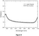
Figure 2 . Surface morphology of saw-damage wafer (a) and laser smoothened (b) wafer. Side view of saw-damaged wafer with apparent micro crack (c) and laser healed silicon wafer with no damage (d).Figure 3 . Pyramid structures on laser-healed silicon surface (a) and saw-damaged (non-treated) silicon surface (b) right after texturing process.Figure 4 . Reflection measurement of pyramid textures on laser healer healed and non-treated silicon wafers.- In present invention, in place of saw damaged healing process using KOH solution, a process where laser beam is irradiated and focused onto the surface is performed. In the process, laser with wavelength of 1064 nm is scanned throughout the wafer. When the laser is incident with the surface of silicon, the heat generated due to absorption of the laser by the silicon melts the surface. In a very short time, the molten silicon recrystallizes and forms a smoother silicon surface. The underneath non-irradiated silicon acts as seed layer for the recrystallization of molten silicon. As the result of the process, smooth surface with relatively much lower surface roughness silicon is obtained. In addition, small crack created in the sawing process have also been removed within the process. Within our developed process, saw damaged etching process can be completely eliminated. This will save extra step in the texturing process of silicon as well as save cost of consumables of chemicals. The clear advantage of the present invention is the elimination of material loss due to chemical etching in saw-damage removal process.
- In addition to laser healing, a process of texturing of silicon surface with KOH solution is also embedded in the present invention. Different size of pyramids structures on single crystal silicon wafers are possible to be fabricated. This is directly related to the fact that the surface morphology of laser healed region is different to that of non-treated region. Indeed, upright pyramids with size less than 3 µm have successfully been fabricated. The proposed process has the advantage of shorter process time to achieve desired surface morphology.
- The present invention proposes a process which involves the usage of laser beam to remove saw-damage region from saw-damaged silicon wafers. This process completely replaces the need of resource-consuming wet chemical etching saw-damage removal process. In addition, the present invention proposes to utilized the laser healed silicon as a starting wafer for silicon texturing process which results in small pyramids size.
- The whole process of the invention starts with laser healing of saw-damaged silicon wafer. A laser beam (Nd-YAG) with wavelength of 1064 nm is focused onto the silicon wafer. The energy from the laser is absorbed by silicon, which in turn, produces heat that is enough to melt the irradiated silicon. At a very short time, the silicon metls and recrystallizes. The underneath silicon which is still intact acts as seed layer for the liquid molten silicon as it recrystallizes. As consequence, the crystal orientation of recrystallized silicon follows the orientation of the starting wafer. To achieve laser healed silicon over the whole wafer, the laser is then scanned throughout the wafer. As the result of this process, a smoother silicon with much less surface roughness is obtained. Small cracks that are originally present in the starting wafer are removed. Similar usage of laser to remove defective region has been demonstrated by Robinson et. al. for the wafers to be used in integrated circuits [2]. In their invention, the requirement of partial vacuum was necessary to minimize oxygen contamination during the laser annealing process which might then become an issue for final semiconductor device. In the present invention, however, ambient environment is sufficient for the annealing process as any oxygen contamination within the top most layer of silicon will be etched away in the proceeding etching process.
- Following the step of laser healing, the silicon wafer is dipped into dilute Hydroflouric (HF) solution as to remove thin silicon dioxide layer. As consequence of performing the laser healing in ambient environment, a thin silicon dioxide may have formed on the surface due to melting of silicon at high temperature. In a separate place, a KOH solution with additive of isopropyl alcohol (IPA) is prepared. The solution is heated up to a certain temperature for texturing process. Right after dipping the wafer in HF solution, the wafer is rinsed in de-ionized water for further cleaning. Shortly afterward, the wafer is immersed in the heated KOH solution to initiate texturing process. An addition of ultrasonic agitation is utilized to improve the result of texturing process.
- Due to the difference in the surface morphology right after laser healing process, different size of pyramids has been obtained. From
Figure 3 , it is clear that the size of pyramids for laser healed surface is much smaller and uniform when compared to pyramids for non-treated surface. As mentioned earlier, different pyramids sizes do not necessarily result in substantial difference in the optical performance. This is clearly depicted inFigure 4 which shows the reflection from both surface with different size of pyramids. - Below steps of the method of invention is given as an example and are not limiting.
- Laser with properties given below (to be an example and are not limiting) is scanned throughout the wafer with separation of each consecutive line ranging from 10 to 30 µm (
figure 1.b ). The power used in the process range from 25% to 30% of the maximum power, to obtain laser healed silicon (figure 1.c )- Type: Nd-YAG laser
- Wavelength: 1064 nm
- Maximum power: 30 W
- Pulse width: < 25 ns
- Repetition rate: 30 kHz
- Beam diameter 50 µm
- The wafer is then immersed into dilute HF solution to remove oxide layer induced in the laser healing process.
- The wafer is put under flowing de-ionized water for rinsing.
- The cleaned wafer is put into mixture of potassium hydroxide and isopropyl alcohol to achieve random upright pyramids with desired size (
figure 1.d ). As an example texturing process, a solution with concentration 4% of KOH + 2% of IPA is used at 70 °C. The etching time for texturing step is 10 minutes. - Agitation using ultrasonic has shown huge improvement in the quality of surface texturing
- Finally, the wafer is rinsed in flowing de-ionized water.
- [1] Y. Han, X. Yu, D. Wang, and D. Yang, "Formation of various pyramidal structures on monocrystalline silicon surface and their influence on the solar cells," J. Nanomater., vol. 2013, 2013.
- [2] J. T. Robinson, O. B. Cecil, and R. R. Shah, "Method for removal of minute physical damage to silicon wafers by employing laser annealing."
US Patent 4,390,392 A, 1980
Claims (4)
- A method of texturing single crystalline silicon wafer comprising step of surface healing by laser irradiation.
- A method according to claim 1 where laser s scanned throughout the wafer with separation of each consecutive line ranging from 10 to 30 µm.
- Method according to claim 1, after laser irradiation, further comprising,a. Immersing the laser scanned wafer into dilute Hydroflouric acid solutionb. Putting under flowing de-ionized waterc. putting into mixture of potassium hydroxide and isopropyl alcohold. rinse in flowing de-ionized water
- Single crystalline silicon wafer obtainable according to claim 1 or 3, having upright pyramids with size smaller than 3 µm.
Applications Claiming Priority (1)
| Application Number | Priority Date | Filing Date | Title |
|---|---|---|---|
| TR2016/20039ATR201620039A1 (en) | 2016-12-29 | 2016-12-29 | A SURFACE TISSUE METHOD USED BY USING A LASER HEAT TREATMENT STEP THAT CONTRIBUTES TO SMALL DIMENSIONAL TISSUE MORPHOLOGY |
Publications (2)
| Publication Number | Publication Date |
|---|---|
| EP3343640A1true EP3343640A1 (en) | 2018-07-04 |
| EP3343640B1 EP3343640B1 (en) | 2020-01-01 |
Family
ID=60450472
Family Applications (1)
| Application Number | Title | Priority Date | Filing Date |
|---|---|---|---|
| EP17203012.4AActiveEP3343640B1 (en) | 2016-12-29 | 2017-11-22 | Method of surface texturing using a laser heating step that contributes to small-sized texture morphology |
Country Status (2)
| Country | Link |
|---|---|
| EP (1) | EP3343640B1 (en) |
| TR (1) | TR201620039A1 (en) |
Cited By (2)
| Publication number | Priority date | Publication date | Assignee | Title |
|---|---|---|---|---|
| DE102018111874A1 (en)* | 2018-05-17 | 2019-11-21 | Hanwha Q Cells Gmbh | A method of treating a sawn semiconductor wafer, semiconductor wafer, and semiconductor wafer solar cell |
| CN111554778A (en)* | 2020-05-13 | 2020-08-18 | 温州大学 | Method for texturing surface of crystalline silicon solar cell by utilizing laser rotary cutting |
Citations (5)
| Publication number | Priority date | Publication date | Assignee | Title |
|---|---|---|---|---|
| US4390392A (en) | 1980-09-16 | 1983-06-28 | Texas Instruments Incorporated | Method for removal of minute physical damage to silicon wafers by employing laser annealing |
| US6451218B1 (en)* | 1998-03-18 | 2002-09-17 | Siemens Solar Gmbh | Method for the wet chemical pyramidal texture etching of silicon surfaces |
| US20090325336A1 (en)* | 2008-04-24 | 2009-12-31 | Malcolm Abbott | Methods for printing an ink on a textured wafer surface |
| US8309389B1 (en)* | 2009-09-10 | 2012-11-13 | Sionyx, Inc. | Photovoltaic semiconductor devices and associated methods |
| US20120295447A1 (en)* | 2010-11-24 | 2012-11-22 | Air Products And Chemicals, Inc. | Compositions and Methods for Texturing of Silicon Wafers |
- 2016
- 2016-12-29TRTR2016/20039Apatent/TR201620039A1/enunknown
- 2017
- 2017-11-22EPEP17203012.4Apatent/EP3343640B1/enactiveActive
Patent Citations (5)
| Publication number | Priority date | Publication date | Assignee | Title |
|---|---|---|---|---|
| US4390392A (en) | 1980-09-16 | 1983-06-28 | Texas Instruments Incorporated | Method for removal of minute physical damage to silicon wafers by employing laser annealing |
| US6451218B1 (en)* | 1998-03-18 | 2002-09-17 | Siemens Solar Gmbh | Method for the wet chemical pyramidal texture etching of silicon surfaces |
| US20090325336A1 (en)* | 2008-04-24 | 2009-12-31 | Malcolm Abbott | Methods for printing an ink on a textured wafer surface |
| US8309389B1 (en)* | 2009-09-10 | 2012-11-13 | Sionyx, Inc. | Photovoltaic semiconductor devices and associated methods |
| US20120295447A1 (en)* | 2010-11-24 | 2012-11-22 | Air Products And Chemicals, Inc. | Compositions and Methods for Texturing of Silicon Wafers |
Non-Patent Citations (1)
| Title |
|---|
| Y. HAN; X. YU; D. WANG; D. YANG: "Formation of various pyramidal structures on monocrystalline silicon surface and their influence on the solar cells", J. NANOMATER., vol. 2013, 2013 |
Cited By (2)
| Publication number | Priority date | Publication date | Assignee | Title |
|---|---|---|---|---|
| DE102018111874A1 (en)* | 2018-05-17 | 2019-11-21 | Hanwha Q Cells Gmbh | A method of treating a sawn semiconductor wafer, semiconductor wafer, and semiconductor wafer solar cell |
| CN111554778A (en)* | 2020-05-13 | 2020-08-18 | 温州大学 | Method for texturing surface of crystalline silicon solar cell by utilizing laser rotary cutting |
Also Published As
| Publication number | Publication date |
|---|---|
| EP3343640B1 (en) | 2020-01-01 |
| TR201620039A1 (en) | 2018-07-23 |
Similar Documents
| Publication | Publication Date | Title |
|---|---|---|
| US6258698B1 (en) | Process for producing semiconductor substrate | |
| JP4416399B2 (en) | Semiconductor wafer processing method for increasing usable planar surface area | |
| US20100029034A1 (en) | Method of manufacturing solar cell | |
| US8084280B2 (en) | Method of manufacturing a solar cell using a pre-cleaning step that contributes to homogeneous texture morphology | |
| EP3139416B1 (en) | Texturing monocrystalline silicon substrates | |
| EP2466650A2 (en) | Method for fabricating silicon wafer solar cell | |
| KR20120011006A (en) | Method for Damage Etching and Texturing of Silicon Single Crystal Substrates | |
| EP2534698B1 (en) | Method for single side texturing | |
| JP4766880B2 (en) | Crystal silicon wafer, crystal silicon solar cell, method for manufacturing crystal silicon wafer, and method for manufacturing crystal silicon solar cell | |
| CN102986020A (en) | Method for finishing silicon on insulator substrate | |
| EP3343640B1 (en) | Method of surface texturing using a laser heating step that contributes to small-sized texture morphology | |
| CN103426736A (en) | Laser chemical order controllable preparation method of monocrystalline silicon inverted pyramid suede | |
| TW201135956A (en) | Surface processing method of silicon substrate for solar cell, and manufacturing method of solar cell | |
| WO2004023567A2 (en) | Method of manufacturing a solar cell | |
| US20130330871A1 (en) | Methods for texturing a semiconductor material | |
| JP2013232581A (en) | Method for manufacturing photovoltaic device and photovoltaic device | |
| Radfar et al. | Effect of laser parameters and post-texturing treatments on the optical and electrical properties of laser textured c-Si wafers | |
| US20020175143A1 (en) | Processes for polishing wafers | |
| CN114566556A (en) | Processing method of semiconductor substrate layer, solar cell and preparation method of solar cell | |
| CN114464571A (en) | Scribing method of gallium oxide polished wafer | |
| JP4412930B2 (en) | Method for manufacturing solar cell element | |
| JP3898599B2 (en) | Manufacturing method of solar cell | |
| CN109755098A (en) | Silicon wafer laser and acid liquor combined texturing process | |
| Grischke et al. | Laser surface texturing for reducing reflection losses in multicristalline silicon solar cells | |
| CN117754144A (en) | Method for splitting silicon carbide crystals using laser scribing assisted cyclic cooling |
Legal Events
| Date | Code | Title | Description |
|---|---|---|---|
| PUAI | Public reference made under article 153(3) epc to a published international application that has entered the european phase | Free format text:ORIGINAL CODE: 0009012 | |
| STAA | Information on the status of an ep patent application or granted ep patent | Free format text:STATUS: THE APPLICATION HAS BEEN PUBLISHED | |
| AK | Designated contracting states | Kind code of ref document:A1 Designated state(s):AL AT BE BG CH CY CZ DE DK EE ES FI FR GB GR HR HU IE IS IT LI LT LU LV MC MK MT NL NO PL PT RO RS SE SI SK SM TR | |
| AX | Request for extension of the european patent | Extension state:BA ME | |
| STAA | Information on the status of an ep patent application or granted ep patent | Free format text:STATUS: REQUEST FOR EXAMINATION WAS MADE | |
| 17P | Request for examination filed | Effective date:20181225 | |
| RBV | Designated contracting states (corrected) | Designated state(s):AL AT BE BG CH CY CZ DE DK EE ES FI FR GB GR HR HU IE IS IT LI LT LU LV MC MK MT NL NO PL PT RO RS SE SI SK SM TR | |
| STAA | Information on the status of an ep patent application or granted ep patent | Free format text:STATUS: EXAMINATION IS IN PROGRESS | |
| 17Q | First examination report despatched | Effective date:20190425 | |
| GRAP | Despatch of communication of intention to grant a patent | Free format text:ORIGINAL CODE: EPIDOSNIGR1 | |
| STAA | Information on the status of an ep patent application or granted ep patent | Free format text:STATUS: GRANT OF PATENT IS INTENDED | |
| INTG | Intention to grant announced | Effective date:20190801 | |
| GRAS | Grant fee paid | Free format text:ORIGINAL CODE: EPIDOSNIGR3 | |
| GRAA | (expected) grant | Free format text:ORIGINAL CODE: 0009210 | |
| STAA | Information on the status of an ep patent application or granted ep patent | Free format text:STATUS: THE PATENT HAS BEEN GRANTED | |
| AK | Designated contracting states | Kind code of ref document:B1 Designated state(s):AL AT BE BG CH CY CZ DE DK EE ES FI FR GB GR HR HU IE IS IT LI LT LU LV MC MK MT NL NO PL PT RO RS SE SI SK SM TR | |
| REG | Reference to a national code | Ref country code:GB Ref legal event code:FG4D | |
| REG | Reference to a national code | Ref country code:CH Ref legal event code:EP Ref country code:AT Ref legal event code:REF Ref document number:1220887 Country of ref document:AT Kind code of ref document:T Effective date:20200115 | |
| REG | Reference to a national code | Ref country code:IE Ref legal event code:FG4D | |
| REG | Reference to a national code | Ref country code:DE Ref legal event code:R096 Ref document number:602017010368 Country of ref document:DE | |
| REG | Reference to a national code | Ref country code:NL Ref legal event code:MP Effective date:20200101 | |
| REG | Reference to a national code | Ref country code:LT Ref legal event code:MG4D | |
| PG25 | Lapsed in a contracting state [announced via postgrant information from national office to epo] | Ref country code:PT Free format text:LAPSE BECAUSE OF FAILURE TO SUBMIT A TRANSLATION OF THE DESCRIPTION OR TO PAY THE FEE WITHIN THE PRESCRIBED TIME-LIMIT Effective date:20200527 Ref country code:FI Free format text:LAPSE BECAUSE OF FAILURE TO SUBMIT A TRANSLATION OF THE DESCRIPTION OR TO PAY THE FEE WITHIN THE PRESCRIBED TIME-LIMIT Effective date:20200101 Ref country code:LT Free format text:LAPSE BECAUSE OF FAILURE TO SUBMIT A TRANSLATION OF THE DESCRIPTION OR TO PAY THE FEE WITHIN THE PRESCRIBED TIME-LIMIT Effective date:20200101 Ref country code:NL Free format text:LAPSE BECAUSE OF FAILURE TO SUBMIT A TRANSLATION OF THE DESCRIPTION OR TO PAY THE FEE WITHIN THE PRESCRIBED TIME-LIMIT Effective date:20200101 Ref country code:CZ Free format text:LAPSE BECAUSE OF FAILURE TO SUBMIT A TRANSLATION OF THE DESCRIPTION OR TO PAY THE FEE WITHIN THE PRESCRIBED TIME-LIMIT Effective date:20200101 Ref country code:RS Free format text:LAPSE BECAUSE OF FAILURE TO SUBMIT A TRANSLATION OF THE DESCRIPTION OR TO PAY THE FEE WITHIN THE PRESCRIBED TIME-LIMIT Effective date:20200101 Ref country code:NO Free format text:LAPSE BECAUSE OF FAILURE TO SUBMIT A TRANSLATION OF THE DESCRIPTION OR TO PAY THE FEE WITHIN THE PRESCRIBED TIME-LIMIT Effective date:20200401 | |
| PG25 | Lapsed in a contracting state [announced via postgrant information from national office to epo] | Ref country code:GR Free format text:LAPSE BECAUSE OF FAILURE TO SUBMIT A TRANSLATION OF THE DESCRIPTION OR TO PAY THE FEE WITHIN THE PRESCRIBED TIME-LIMIT Effective date:20200402 Ref country code:BG Free format text:LAPSE BECAUSE OF FAILURE TO SUBMIT A TRANSLATION OF THE DESCRIPTION OR TO PAY THE FEE WITHIN THE PRESCRIBED TIME-LIMIT Effective date:20200401 Ref country code:HR Free format text:LAPSE BECAUSE OF FAILURE TO SUBMIT A TRANSLATION OF THE DESCRIPTION OR TO PAY THE FEE WITHIN THE PRESCRIBED TIME-LIMIT Effective date:20200101 Ref country code:SE Free format text:LAPSE BECAUSE OF FAILURE TO SUBMIT A TRANSLATION OF THE DESCRIPTION OR TO PAY THE FEE WITHIN THE PRESCRIBED TIME-LIMIT Effective date:20200101 Ref country code:LV Free format text:LAPSE BECAUSE OF FAILURE TO SUBMIT A TRANSLATION OF THE DESCRIPTION OR TO PAY THE FEE WITHIN THE PRESCRIBED TIME-LIMIT Effective date:20200101 Ref country code:IS Free format text:LAPSE BECAUSE OF FAILURE TO SUBMIT A TRANSLATION OF THE DESCRIPTION OR TO PAY THE FEE WITHIN THE PRESCRIBED TIME-LIMIT Effective date:20200501 | |
| REG | Reference to a national code | Ref country code:DE Ref legal event code:R097 Ref document number:602017010368 Country of ref document:DE | |
| PG25 | Lapsed in a contracting state [announced via postgrant information from national office to epo] | Ref country code:ES Free format text:LAPSE BECAUSE OF FAILURE TO SUBMIT A TRANSLATION OF THE DESCRIPTION OR TO PAY THE FEE WITHIN THE PRESCRIBED TIME-LIMIT Effective date:20200101 Ref country code:DK Free format text:LAPSE BECAUSE OF FAILURE TO SUBMIT A TRANSLATION OF THE DESCRIPTION OR TO PAY THE FEE WITHIN THE PRESCRIBED TIME-LIMIT Effective date:20200101 Ref country code:EE Free format text:LAPSE BECAUSE OF FAILURE TO SUBMIT A TRANSLATION OF THE DESCRIPTION OR TO PAY THE FEE WITHIN THE PRESCRIBED TIME-LIMIT Effective date:20200101 Ref country code:SM Free format text:LAPSE BECAUSE OF FAILURE TO SUBMIT A TRANSLATION OF THE DESCRIPTION OR TO PAY THE FEE WITHIN THE PRESCRIBED TIME-LIMIT Effective date:20200101 Ref country code:SK Free format text:LAPSE BECAUSE OF FAILURE TO SUBMIT A TRANSLATION OF THE DESCRIPTION OR TO PAY THE FEE WITHIN THE PRESCRIBED TIME-LIMIT Effective date:20200101 Ref country code:RO Free format text:LAPSE BECAUSE OF FAILURE TO SUBMIT A TRANSLATION OF THE DESCRIPTION OR TO PAY THE FEE WITHIN THE PRESCRIBED TIME-LIMIT Effective date:20200101 | |
| PLBE | No opposition filed within time limit | Free format text:ORIGINAL CODE: 0009261 | |
| STAA | Information on the status of an ep patent application or granted ep patent | Free format text:STATUS: NO OPPOSITION FILED WITHIN TIME LIMIT | |
| REG | Reference to a national code | Ref country code:AT Ref legal event code:MK05 Ref document number:1220887 Country of ref document:AT Kind code of ref document:T Effective date:20200101 | |
| 26N | No opposition filed | Effective date:20201002 | |
| PG25 | Lapsed in a contracting state [announced via postgrant information from national office to epo] | Ref country code:AT Free format text:LAPSE BECAUSE OF FAILURE TO SUBMIT A TRANSLATION OF THE DESCRIPTION OR TO PAY THE FEE WITHIN THE PRESCRIBED TIME-LIMIT Effective date:20200101 Ref country code:IT Free format text:LAPSE BECAUSE OF FAILURE TO SUBMIT A TRANSLATION OF THE DESCRIPTION OR TO PAY THE FEE WITHIN THE PRESCRIBED TIME-LIMIT Effective date:20200101 | |
| PG25 | Lapsed in a contracting state [announced via postgrant information from national office to epo] | Ref country code:PL Free format text:LAPSE BECAUSE OF FAILURE TO SUBMIT A TRANSLATION OF THE DESCRIPTION OR TO PAY THE FEE WITHIN THE PRESCRIBED TIME-LIMIT Effective date:20200101 Ref country code:SI Free format text:LAPSE BECAUSE OF FAILURE TO SUBMIT A TRANSLATION OF THE DESCRIPTION OR TO PAY THE FEE WITHIN THE PRESCRIBED TIME-LIMIT Effective date:20200101 | |
| PG25 | Lapsed in a contracting state [announced via postgrant information from national office to epo] | Ref country code:MC Free format text:LAPSE BECAUSE OF FAILURE TO SUBMIT A TRANSLATION OF THE DESCRIPTION OR TO PAY THE FEE WITHIN THE PRESCRIBED TIME-LIMIT Effective date:20200101 | |
| REG | Reference to a national code | Ref country code:CH Ref legal event code:PL | |
| PG25 | Lapsed in a contracting state [announced via postgrant information from national office to epo] | Ref country code:LU Free format text:LAPSE BECAUSE OF NON-PAYMENT OF DUE FEES Effective date:20201122 | |
| REG | Reference to a national code | Ref country code:BE Ref legal event code:MM Effective date:20201130 | |
| PG25 | Lapsed in a contracting state [announced via postgrant information from national office to epo] | Ref country code:LI Free format text:LAPSE BECAUSE OF NON-PAYMENT OF DUE FEES Effective date:20201130 Ref country code:CH Free format text:LAPSE BECAUSE OF NON-PAYMENT OF DUE FEES Effective date:20201130 | |
| PG25 | Lapsed in a contracting state [announced via postgrant information from national office to epo] | Ref country code:IE Free format text:LAPSE BECAUSE OF NON-PAYMENT OF DUE FEES Effective date:20201122 | |
| PGFP | Annual fee paid to national office [announced via postgrant information from national office to epo] | Ref country code:TR Payment date:20211005 Year of fee payment:5 Ref country code:DE Payment date:20211109 Year of fee payment:5 Ref country code:FR Payment date:20211109 Year of fee payment:5 | |
| PG25 | Lapsed in a contracting state [announced via postgrant information from national office to epo] | Ref country code:MT Free format text:LAPSE BECAUSE OF FAILURE TO SUBMIT A TRANSLATION OF THE DESCRIPTION OR TO PAY THE FEE WITHIN THE PRESCRIBED TIME-LIMIT Effective date:20200101 Ref country code:CY Free format text:LAPSE BECAUSE OF FAILURE TO SUBMIT A TRANSLATION OF THE DESCRIPTION OR TO PAY THE FEE WITHIN THE PRESCRIBED TIME-LIMIT Effective date:20200101 | |
| PG25 | Lapsed in a contracting state [announced via postgrant information from national office to epo] | Ref country code:MK Free format text:LAPSE BECAUSE OF FAILURE TO SUBMIT A TRANSLATION OF THE DESCRIPTION OR TO PAY THE FEE WITHIN THE PRESCRIBED TIME-LIMIT Effective date:20200101 Ref country code:AL Free format text:LAPSE BECAUSE OF FAILURE TO SUBMIT A TRANSLATION OF THE DESCRIPTION OR TO PAY THE FEE WITHIN THE PRESCRIBED TIME-LIMIT Effective date:20200101 | |
| GBPC | Gb: european patent ceased through non-payment of renewal fee | Effective date:20211122 | |
| PG25 | Lapsed in a contracting state [announced via postgrant information from national office to epo] | Ref country code:BE Free format text:LAPSE BECAUSE OF NON-PAYMENT OF DUE FEES Effective date:20201130 | |
| PG25 | Lapsed in a contracting state [announced via postgrant information from national office to epo] | Ref country code:GB Free format text:LAPSE BECAUSE OF NON-PAYMENT OF DUE FEES Effective date:20211122 | |
| REG | Reference to a national code | Ref country code:DE Ref legal event code:R119 Ref document number:602017010368 Country of ref document:DE | |
| PG25 | Lapsed in a contracting state [announced via postgrant information from national office to epo] | Ref country code:DE Free format text:LAPSE BECAUSE OF NON-PAYMENT OF DUE FEES Effective date:20230601 | |
| PG25 | Lapsed in a contracting state [announced via postgrant information from national office to epo] | Ref country code:FR Free format text:LAPSE BECAUSE OF NON-PAYMENT OF DUE FEES Effective date:20221130 | |
| PG25 | Lapsed in a contracting state [announced via postgrant information from national office to epo] | Ref country code:TR Free format text:LAPSE BECAUSE OF NON-PAYMENT OF DUE FEES Effective date:20221122 |