EP3326692A1 - Feedthrough for an implantable medical device having a composite conductive lead - Google Patents
Feedthrough for an implantable medical device having a composite conductive leadDownload PDFInfo
- Publication number
- EP3326692A1 EP3326692A1EP17197151.8AEP17197151AEP3326692A1EP 3326692 A1EP3326692 A1EP 3326692A1EP 17197151 AEP17197151 AEP 17197151AEP 3326692 A1EP3326692 A1EP 3326692A1
- Authority
- EP
- European Patent Office
- Prior art keywords
- feedthrough
- capacitor
- ferrule
- metallization
- disposed
- Prior art date
- Legal status (The legal status is an assumption and is not a legal conclusion. Google has not performed a legal analysis and makes no representation as to the accuracy of the status listed.)
- Granted
Links
Images


Classifications
- A—HUMAN NECESSITIES
- A61—MEDICAL OR VETERINARY SCIENCE; HYGIENE
- A61N—ELECTROTHERAPY; MAGNETOTHERAPY; RADIATION THERAPY; ULTRASOUND THERAPY
- A61N1/00—Electrotherapy; Circuits therefor
- A61N1/18—Applying electric currents by contact electrodes
- A61N1/32—Applying electric currents by contact electrodes alternating or intermittent currents
- A61N1/36—Applying electric currents by contact electrodes alternating or intermittent currents for stimulation
- A61N1/372—Arrangements in connection with the implantation of stimulators
- A61N1/375—Constructional arrangements, e.g. casings
- A61N1/3752—Details of casing-lead connections
- A61N1/3754—Feedthroughs
- H—ELECTRICITY
- H01—ELECTRIC ELEMENTS
- H01G—CAPACITORS; CAPACITORS, RECTIFIERS, DETECTORS, SWITCHING DEVICES, LIGHT-SENSITIVE OR TEMPERATURE-SENSITIVE DEVICES OF THE ELECTROLYTIC TYPE
- H01G4/00—Fixed capacitors; Processes of their manufacture
- H01G4/002—Details
- H01G4/018—Dielectrics
- H—ELECTRICITY
- H01—ELECTRIC ELEMENTS
- H01G—CAPACITORS; CAPACITORS, RECTIFIERS, DETECTORS, SWITCHING DEVICES, LIGHT-SENSITIVE OR TEMPERATURE-SENSITIVE DEVICES OF THE ELECTROLYTIC TYPE
- H01G4/00—Fixed capacitors; Processes of their manufacture
- H01G4/002—Details
- H01G4/224—Housing; Encapsulation
- H—ELECTRICITY
- H01—ELECTRIC ELEMENTS
- H01G—CAPACITORS; CAPACITORS, RECTIFIERS, DETECTORS, SWITCHING DEVICES, LIGHT-SENSITIVE OR TEMPERATURE-SENSITIVE DEVICES OF THE ELECTROLYTIC TYPE
- H01G4/00—Fixed capacitors; Processes of their manufacture
- H01G4/002—Details
- H01G4/228—Terminals
- H01G4/236—Terminals leading through the housing, i.e. lead-through
- H—ELECTRICITY
- H01—ELECTRIC ELEMENTS
- H01G—CAPACITORS; CAPACITORS, RECTIFIERS, DETECTORS, SWITCHING DEVICES, LIGHT-SENSITIVE OR TEMPERATURE-SENSITIVE DEVICES OF THE ELECTROLYTIC TYPE
- H01G4/00—Fixed capacitors; Processes of their manufacture
- H01G4/35—Feed-through capacitors or anti-noise capacitors
- H—ELECTRICITY
- H01—ELECTRIC ELEMENTS
- H01G—CAPACITORS; CAPACITORS, RECTIFIERS, DETECTORS, SWITCHING DEVICES, LIGHT-SENSITIVE OR TEMPERATURE-SENSITIVE DEVICES OF THE ELECTROLYTIC TYPE
- H01G4/00—Fixed capacitors; Processes of their manufacture
- H01G4/40—Structural combinations of fixed capacitors with other electric elements, the structure mainly consisting of a capacitor, e.g. RC combinations
- H—ELECTRICITY
- H05—ELECTRIC TECHNIQUES NOT OTHERWISE PROVIDED FOR
- H05K—PRINTED CIRCUITS; CASINGS OR CONSTRUCTIONAL DETAILS OF ELECTRIC APPARATUS; MANUFACTURE OF ASSEMBLAGES OF ELECTRICAL COMPONENTS
- H05K1/00—Printed circuits
- H05K1/18—Printed circuits structurally associated with non-printed electric components
- H05K1/181—Printed circuits structurally associated with non-printed electric components associated with surface mounted components
- H—ELECTRICITY
- H01—ELECTRIC ELEMENTS
- H01G—CAPACITORS; CAPACITORS, RECTIFIERS, DETECTORS, SWITCHING DEVICES, LIGHT-SENSITIVE OR TEMPERATURE-SENSITIVE DEVICES OF THE ELECTROLYTIC TYPE
- H01G4/00—Fixed capacitors; Processes of their manufacture
- H01G4/002—Details
- H01G4/005—Electrodes
- H01G4/012—Form of non-self-supporting electrodes
- H—ELECTRICITY
- H05—ELECTRIC TECHNIQUES NOT OTHERWISE PROVIDED FOR
- H05K—PRINTED CIRCUITS; CASINGS OR CONSTRUCTIONAL DETAILS OF ELECTRIC APPARATUS; MANUFACTURE OF ASSEMBLAGES OF ELECTRICAL COMPONENTS
- H05K2201/00—Indexing scheme relating to printed circuits covered by H05K1/00
- H05K2201/10—Details of components or other objects attached to or integrated in a printed circuit board
- H05K2201/10007—Types of components
- H05K2201/10015—Non-printed capacitor
Definitions
- the present inventiongenerally relates to implantable medical devices and hermetic terminal subassemblies. More particularly, the present invention relates a hermetic terminal having a composite conductive lead brazed into an insulator body.
- AIMDsactive implantable medical devices
- Such devicesinclude cardiac pacemakers, cardiac defibrillators, cardioverters, neurostimulators, and other devices for delivering and/or receiving electrical signals to/from a portion of the body.
- Sensing and/or stimulating leadsextend from the associated implantable medical device to a distal tip electrode or electrodes in contact with body tissue.
- Hermetic terminal or feedthrough of these implantable devicesis considered critical.
- Hermetic terminals or feedthroughsare generally well-known in the art for connecting electrical signals through the housing or case of an AIMD.
- a hermetic terminalcomprises one or more conductive pathways which may include conductive terminal pins, conductive filled vias, leadwires and the like supported by an insulative structure for feedthrough passage from the exterior to the interior of an AIMD electromagnetic shield housing.
- Hermetic terminals or feedthroughs for AIMDsmust be biocompatible as well as resistant to degradation under applied bias current or voltage (biostable).
- Hermeticity of the feedthroughis imparted by judicious material selection and carefully prescribed manufacturing processing. Sustainable hermeticity of the feedthrough over the lifetime of these implantable devices is critical because the hermetic terminal intentionally isolates the internal circuitry and components of the device (AIMD) from the external body fluid environment to which the component is exposed. In particular, the hermetic terminal isolates the internal circuitry, connections, power sources and other components in the device from ingress of body fluids. Ingress of body fluids into an implantable medical device is known to be a contributing factor to device malfunction and may contribute to the compromise or failure of electrical circuitry, connections, power sources and other components within an implantable medical device that are necessary for consistent and reliable device therapy delivery to a patient. Furthermore, ingress of body fluids may compromise an implantable medical device's functionality which may constitute electrical shorting, element or joint corrosion, metal migration or other such harmful consequences affecting consistent and reliable device therapy delivery.
- hermetic terminal or feedthrough pinsare typically connected to one or more lead conductors of implantable therapy delivery leads.
- implantable therapy delivery leadscan effectively act as antennas that receive electromagnetic interference (EMI) signals. Therefore, when these electromagnetic signals enter within the interior space of a hermetic implantable medical device, facilitated by the therapy delivery leads, they can negatively impact the intended function of the medical device and as a result, negatively impact therapy delivery intended for a patient by that device.
- EMI engineerscommonly refer to this as the "genie in the bottle” effect. In other words, once the genie (i.e., EMI) is inside the hermetic housing of the device, it can wreak havoc with electronic circuit functions by cross-coupling and re-radiating within the device.
- MRI RF electrical currents imposed on the implanted therapy delivery leadscan cause the leads to heat to the point where tissue damage is likely.
- MRI induced RF currentselectromagnetic interference-EMI
- implanted therapy delivery leadsresulting in undesirable electrical currents which can enter the AIMD and can disrupt or damage the sensitive electronics within the implantable medical device.
- materials selection and fabrication processing parametersare of utmost importance in creating a hermetic terminal (or feedthrough) or a structure embodying a hermetic terminal (or feedthrough), that can survive anticipated and possibly catastrophically damaging environmental conditions and that can be practically and cost effectively manufactured.
- hermetic terminal subassemblies for AIMDscomprise a titanium ferrule and a gold brazed alumina insulator.
- hermetic terminalsmay comprise a ferrule and a compression or fusion glass seal.
- Hermetic terminals or feedthrough assemblies utilizing ceramic dielectric materialsmay fail in a brittle manner. A brittle failure typically occurs when the ceramic structure is deformed elastically up to an intolerable stress, at which point the ceramic fails catastrophically. Most brittle failures occur by crack propagation in a tensile stress field. Even microcracking caused by sufficiently high tensile stress concentrations may result in a catastrophic failure including loss of hermeticity identified as critical in hermetic terminals for implantable medical devices.
- Loss of hermeticitymay be a result of design aspects such as a sharp comer which creates a stress riser, mating materials with a difference of coefficient of thermal expansions (CTE) that generate tensile stresses that ultimately result in loss of hermeticity of the feedthrough or interconnect structure.
- CTEcoefficient of thermal expansions
- a tensile stress limit for a given ceramic based hermetic design structurecannot be specified because failure stress in these structures is not a constant.
- variables affecting stress levelsinclude the design itself, the materials selection, symmetry of the feedthrough, and the bonding characteristics of mating surfaces within the feedthrough.
- length, width and height of the overall ceramic structurematters as do the number, spacing, length and diameter of the conductive pathways (vias, terminal pins, leadwires, etc.) in that structure.
- the selection of the mating materialsthat is, the material that fills the vias (or leadwire) and the material that forms the base ceramic, are important.
- the fabrication processing parametersparticularly at binder burnout, sintering and cool down, make a difference.
- high reliabilityis required in an application such as indicated with hermetic terminals or feedthroughs for AIMDs, to provide insurance for a very low probability of failure it is necessary to design a hermetic terminal assembly or feedthrough structure so that stresses imparted by design, materials and/or processing are limited to a smaller level of an average possible failure stress.
- hermetic terminals and structurescomprising hermetic terminals for AIMDs wherein the demand for biocompatibility exists, this task becomes even more difficult.
- a hermetic feedthroughcomprising a monolithic alumina insulator substrate within which a platinum, palladium or the like conductive pathway or via resides or wherein a metallic leadwire (terminal pin) resides. More specifically in the case of a filled via, the present invention provides a hermetic feedthrough in which the hermetic seal is created through the intimate bonding of a CERMET (ceramic metal) or a platinum metal residing within the alumina substrate.
- a traditional ceramic-to-metal hermetic terminalis an assembly of three components: electrical conductors (leadwires, pins, terminal pins, filled vias) that conduct electrical current, a ceramic insulator, and a metal housing, which is referred to as the flange or the ferrule (or even the AIMD housing itself).
- Brazed jointstypically hermetically seal the metal leadwires and the flange or ferrule to the ceramic insulator.
- the braze materialis generally intended to deform in a ductile manner in order to compensate for perturbations that stress the bond between the mating materials as the braze material may provide ductile strain relief when the thermal expansion mismatch between the ceramic and metal is large.
- mating materials with large mismatches in CTEcan be coupled through braze materials whose high creep rate and low yield strength reduce the stresses generated by the differential contraction existing between these mating materials.
- Glass sealsare also known in the art, which form a hermetic seal to the ferrule and one or more leadwires passing through the glass seal.
- a terminal or feedthrough capacitor EMI filtermay be disposed at, near or within a hermetic terminal or feedthrough resulting in a feedthrough filter capacitor which diverts high frequency electrical signals from lead conductors to the housing or case of an AIMD.
- feedthrough capacitor EMI filtersMany different insulator structures and related mounting methods are known in the art for use of feedthrough capacitor EMI filters in AIMDs, wherein the insulative structure also provides a hermetic terminal or feedthrough to prevent entry of body fluids into the housing of an AIMD.
- the hermetic terminal subassemblyhas been combined in various ways with a ceramic feedthrough filter EMI capacitor to decouple interference signals to the housing of the medical device.
- a round/discoidal (or rectangular) ceramic feedthrough EMI filter capacitoris combined with a hermetic terminal pin assembly to suppress and decouple undesired interference or noise transmission along a terminal pin.
- the feedthrough capacitoris coaxial having two sets of electrode plates embedded in spaced relation within an insulative dielectric substrate or base, formed typically as a ceramic monolithic structure. One set of the electrode plates are electrically connected at an inner diameter cylindrical surface of the coaxial capacitor structure to the conductive terminal pin utilized to pass the desired electrical signal or signals.
- the other or second set of electrode platesare coupled at an outer diameter surface of the round/discoidal capacitor to a cylindrical ferrule of conductive material, wherein the ferrule is electrically connected in turn to the conductive housing of the electronic device.
- the number and dielectric thickness spacing of the electrode plate setsvaries in accordance with the capacitance value and the voltage rating of the coaxial capacitor.
- the outer feedthrough capacitor electrode plate sets(or "ground” plates) are coupled in parallel together by a metalized layer which is fired, sputtered or plated onto the ceramic capacitor. This metalized band, in turn, is coupled to the ferrule by conductive adhesive, soldering, brazing, welding, or the like.
- the inner feedthrough capacitor electrode plate setsare coupled in parallel together by a metalized layer which is either glass frit fired or plated onto the ceramic capacitor.
- This metalized bandis mechanically and electrically coupled to the lead wire(s) by conductive adhesive, soldering, or the like.
- the coaxial capacitorpermits passage of relatively low frequency biologic signals along the terminal pin, while shielding and decoupling/attenuating undesired interference signals of typically high frequency to the AIMD conductive housing.
- Feedthrough capacitors of this general typeare available in unipolar (one), bipolar (two), tripolar (three), quadpolar (four), pentapolar (five), hexpolar (6) and additional lead configurations.
- the feedthrough capacitors(in both discoidal and rectangular configurations) of this general type are commonly employed in implantable cardiac pacemakers and defibrillators and the like, wherein the pacemaker housing is constructed from a biocompatible metal such as titanium alloy, which is electrically and mechanically coupled to the ferrule of the hermetic terminal pin assembly which is in turn electrically coupled to the coaxial feedthrough filter capacitor.
- the filter capacitor and terminal pin assemblyprevents entrance of interference signals to the interior of the pacemaker housing, wherein such interference signals could otherwise adversely affect the desired cardiac pacing or defibrillation function.
- the hermetic terminal subassemblyincludes conductive pathways (leadwires, pins, terminal pins, filled vias, etc.) to hermetically pass through the insulator in non-conductive relation with the ferrule or the AIMD housing.
- the conductive pathwaysalso pass through the feedthrough hole of the capacitor to electronic circuits disposed inside of the AIMD housing.
- these conductive pathwaysare constructed of platinum or platinum-iridium, palladium or palladium-iridium, niobium pins or filled vias with conductive powders, ceramics, gradient materials or the like.
- Platinum-iridiumis an ideal choice because it is biocompatible, non-toxic and is also mechanically very strong. The iridium is added to enhance material stiffness and to enable the hermetic terminal subassembly leadwire to sustain bending stresses.
- An issue with the use of platinum for leadwiresis that platinum has become extremely expensive and may be subject to premature fracture under rigorous processing such as ultrasonic cleaning or application use/misuse, possibly unintentional damaging forces resulting from Twiddler's Syndrome. Twiddler's Syndrome is a situation documented in the literature where a patient will unconsciously or knowingly twist the implantable device to the point where attached leads may even fracture.
- a hermetic seal subassemblywhich has a biocompatible and non-toxic lead or leadwire on the body fluid side, which is co-joined within the hermetic seal insulator to a lower cost device side lead, which may be routed to AIMD internal electronic circuits.
- the present inventiondoes not change the way the prior art leadwires are generally connected to a body fluid side header block or implantable lead.
- the present inventionalso does not change the way that leadwires may be routed inside the device and connected directly to an AIMD electronic circuit board or to an intermediate flex cable or the like.
- a hermetically sealed feedthrough subassemblyis attachable to an active implantable medical device (AIMD), the feedthrough subassembly comprising: (a) an insulator substrate assembly, comprising: i) an insulator body defined as having a first insulator side opposite a second insulator side, the first insulator side and second insulator side separated and connected by at least one outside surface; ii) at least one via hole disposed through the insulator body extending from the first insulator side to the second insulator side; iii) an internal metallization formed at least partially on an inside of the at least one via hole; iv) a first conductive leadwire having a first conductive leadwire first end at least partially disposed within the at least one via hole and having a first conductive leadwire second end disposed past the first insulator side; v) a second conductive leadwire having a second conductive leadwire first end at least partially disposed within the at least one via
- exemplary embodimentsmay include a feedthrough filter capacitor disposed on the second insulator side, the feedthrough filter capacitor comprising: i) at least one active electrode plate disposed parallel and spaced from at least one ground electrode plate, wherein the plates are disposed within a capacitor dielectric substrate; ii) a first passageway disposed through the capacitor dielectric substrate and disposed perpendicular to the plates; iii) a capacitor internal metallization disposed within the first passageway electrically connected to the at least one active electrode plate and in non-conductive relation with the at least one ground electrode plate; iv) a capacitor external metallization disposed on an outside surface of the capacitor dielectric substrate and electrically connected to the at least one ground electrode plate and in non-conductive relation with the at least one active electrode plate.
- Other exemplary embodimentsmay include a third conductive leadwire having a third conductive leadwire first end at least partially disposed within the first passageway of the feedthrough filter capacitor and having a third conductive leadwire second end disposed past the feedthrough filter capacitor configured to be connectable to electronics internal to the AIMD, wherein the second conductive leadwire second end is at least partially disposed within the first passageway of the feedthrough filter capacitor, wherein the second conductive leadwire second end is at, near or adjacent to the third conductive leadwire first end.
- exemplary embodimentsmay include a first electrically conductive material forming at least a three-way electrical connection electrically connecting the second conductive leadwire second end, the third conductive leadwire first end and the capacitor internal metallization.
- the first electrically conductive materialmay be selected from the group consisting of a solder, a solder BGA, a solder paste, an epoxy, and a polyimide.
- exemplary embodimentsmay include a second electrically conductive material electrically connecting the capacitor external metallization to the ferrule and/or to the second braze.
- exemplary embodimentsmay include at least one internal ground plate disposed within the insulator body electrically connecting the internal metallization formed at least partially on the inside of the at least one via hole to the external metallization disposed at least partially on the at least one outside surface of the insulator body.
- the first braze and second brazemay be formed at the same time and are connected by a braze channel.
- a conductive clipmay be electrically coupled between and to the second conductive leadwire and the ferrule.
- the ferrulemay include a conductive peninsula extending at least partially into the ferrule opening, wherein the second conductive leadwire is electrically coupled to the conductive peninsula with the first braze.
- exemplary embodimentsmay include a chip capacitor disposed on the second insulator side, the chip capacitor comprising: i) at least one active electrode plate disposed parallel and spaced from at least one ground electrode plate, wherein the plates are disposed within a capacitor dielectric substrate; ii) a first capacitor metallization disposed on one end of the chip capacitor and electrically connected to the at least one active electrode plate and in non-conductive relation with the at least one ground electrode plate; iii) a second capacitor metallization disposed on another end of the chip capacitor and electrically connected to the at least one ground electrode plate and in non-conductive relation with the at least one active electrode plate.
- exemplary embodimentsmay include a first electrically conductive material electrically coupling the first capacitor metallization to the second conductive leadwire.
- Other exemplary embodimentsmay include a second electrically conductive material electrically coupling the second capacitor metallization to the ferrule and/or the second gold braze.
- the chip capacitormay be attached to the insulator body.
- the chip capacitormay be attached to a circuit board, wherein the circuit board is attached to the insulator body.
- Other exemplary embodimentsmay include an oxide-resistant metal addition, wherein a second electrically conductive material electrically couples the second capacitor metallization to the oxide resistant metal addition, and wherein a third electrically conductive material electrically connects the oxide-resistant metal addition to the ferrule or wherein the oxide-resistant metal addition is welded to the ferrule.
- the second conductive leadwiremay comprise platinum or palladium.
- the first conductive leadwiremay comprise niobium or tantalum.
- the first braze and second brazemay each comprise a gold braze.
- the first brazemay be disposed at or near the second insulator side and does not extend to at or near the first insulator side.
- the first brazemay be disposed at or near the first insulator side and may not extend to at or near the second insulator side.
- the third conductive leadwire first endmay be pre-tinned.
- the first and second hermetic sealsmay have a leak rate no greater than 1 x 10 -7 std cc He/sec.
- the external metallizationmay be disposed at least partially on the at least one outside surface of the insulator body comprises an adhesion metallization and a wetting metallization, wherein the adhesion metallization may be disposed at least partially on the at least one outside surface of the insulator body and wherein the wetting metallization may be disposed on the adhesion metallization.
- exemplary embodimentsmay include an insulative washer which may be disposed between the insulator substrate assembly and the feedthrough filter capacitor.
- the ferrulemay be configured to be joined to an AIMD housing by a laser weld or braze.
- the ferrulemay be formed from and as a continuous part of an AIMD housing.
- the first insulator sidemay be a body fluid side and the second insulator side may be a device side.
- an insulative feedthrough attachable to an active implantable medical devicecomprises: a feedthrough body comprising a material which is both electrically insulative and biocompatible, wherein the feedthrough body is configured to be hermetically installed within the active implantable medical device separating a body fluid side from a device side; a passageway disposed through the feedthrough body extending from the body fluid side to the device side; a composite conductor disposed within the passageway, the composite conductor comprising a body fluid side metallic wire electrically conductive to a device side metallic wire; wherein the body fluid side metallic wire extends from a first end disposed inside the passageway to a second end on the body fluid side; wherein the device side metallic wire extends from a first end disposed inside the passageway to a second end on the device side; wherein the body fluid side metallic wire is hermetically sealed to the feedthrough body; wherein the body fluid side metallic wire is biocompatible; and wherein the body fluid side metallic wire is not the same material as the device side
- the ferrulemay be made from an electrically conductive material, the ferrule configured to be hermetically sealed to a housing of the implantable medical device, wherein the ferrule defines a ferrule opening and the feedthrough body is hermetically sealed to the ferrule closing the ferrule opening.
- the ferrulemay comprise titanium.
- An adhesion layermay be disposed on an outside surface of the feedthrough body, a wetting layer may be disposed on the adhesion layer, and a gold braze may be hermetically sealing the wetting layer to the ferrule.
- the ferrule openingmay define an inner ferrule surface, wherein the feedthrough body is at least partially disposed within ferrule opening and hermetically sealed by the gold braze to the ferrule inner surface.
- the device side metallic wiremay not biocompatible.
- the device side metallic wiremay be platinum.
- the device side metallic wire comprising platinummay not include iridium.
- the second end of the body fluid side metallic wiremay extend past the feedthrough body on the body fluid side.
- the second end of the device side metallic wiremay extend past the feedthrough body on the device side.
- the second end of the body fluid side metallic wiremay be aligned with a body fluid side surface of the feedthrough body.
- the second end of the device side metallic wiremay be aligned with a device side surface of the feedthrough body.
- the second end of the body fluid side metallic wiremay be recessed from a body fluid side surface of the feedthrough body.
- the second end of the device side metallic wiremay be recessed from a device side surface of the feedthrough body.
- the first end of the body fluid side metallic wiremay be soldered or welded to the first end of the device side metallic wire.
- An adhesion layermay be disposed on an inside surface of the passageway, a wetting layer may be disposed on the adhesion layer, and a gold braze may hermetically seal the wetting layer to the body fluid side metallic wire.
- the gold brazemay be connected to the device side metallic wire.
- a capacitormay be disposed on the device side of the feedthrough body, wherein the capacitor comprises at least one active electrode plate and at least one ground electrode plate disposed within a capacitor dielectric, wherein an active end metallization is electrically connected to the at least one active electrode plate and a ground end metallization is electrically connected to the at least one ground electrode plate.
- the active end metallizationmay be in electrical communication with the device side metallic wire, and wherein the ground end metallization may be in electrical communication with the ferrule.
- the capacitormay be a chip capacitor.
- the chip capacitormay be mounted to the feedthrough body.
- the chip capacitormay be mounted to a circuit board, wherein the circuit board is mounted to the feedthrough body.
- the capacitormay be a feedthrough capacitor.
- the capacitormay be mounted to an adhesive washer and the adhesive washer is mounted to the feedthrough body.
- the second end of the device side metallic wiremay extend past the feedthrough body on the device side and is disposed within a metallized via formed through the feedthrough capacitor, wherein the metallization of the metallized via comprises the active end metallization.
- a third wiremay be disposed on the device side and extending at least partially into the metallized via.
- a conductive materialmay be electrically connected to the second end of the device side metallic wire, to the third wire and to the active end metallization of the capacitor.
- An internally grounded capacitormay be disposed on the device side of the feedthrough body, wherein the capacitor comprises at least one active electrode plate and at least one ground electrode plate disposed within a capacitor dielectric, wherein an active end metallization is electrically connected to the at least one active electrode plate and a ground end metallization is electrically connected to the at least one ground electrode plate, wherein the active end metallization is formed within an active via disposed through the capacitor dielectric and the ground end metallization is formed within a ground via disposed through the capacitor, wherein the capacitor does not have an external metallization on an outside surface of the capacitor dielectric.
- the feedthrough bodymay comprise a conductive pathway in electrical communication with the ferrule on one end of the conductive pathway and in electrical communication with the ground end metallization on the other end of the electrical pathway.
- the conductive pathwaymay comprise a gold braze. The gold braze may also hermetically seals the feedthrough body to the ferrule.
- the conductive pathwaymay comprise at least one conductive grounding layer disposed with the feedthrough body.
- a conductive pinmay be in electrical communication to the ground end metallization on one end of the conductive pin and in electrical communication with the conductive pathway on the other end of the conductive pin.
- a ferrulemay be made from a conductive material, the ferrule configured to be hermetically sealed to a housing of the implantable medical device, wherein the ferrule defines a ferrule opening and the feedthrough body is hermetically sealed to the ferrule closing the ferrule opening; including a feedthrough capacitor disposed on the device side of the feedthrough body, wherein the capacitor comprises at least one active electrode plate and at least one ground electrode plate disposed within a capacitor dielectric, wherein an active end metallization is electrically connected to the at least one active electrode plate and a ground end metallization is electrically connected to the at least one ground electrode plate; including a gold braze attached to the ferrule on the device side; and including an electrically conductive fill connecting the ground end metallization to the gold braze.
- the feedthrough bodymay comprise a glass insulator, wherein the hermetic seal between the feedthrough body and the ferrule is formed at the same time as the hermetic seal between the composite conductor and the feedthrough body.
- An alumina washerdisposed over the feedthrough body on the body fluid side.
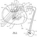
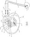
- FIG. 1illustrates various types of active implantable and external medical devices 100 that are currently in use.
- FIG. 1is a wire formed diagram of a generic human body showing a number of implanted medical devices.
- 100Ais a family of external and implantable hearing devices which can include the group of hearing aids, cochlear implants, piezoelectric sound bridge transducers and the like.
- 100Bincludes an entire variety of neurostimulators and brain stimulators.
- Neurostimulatorsare used to stimulate the Vagus nerve, for example, to treat epilepsy, obesity and depression.
- Brain stimulatorsare similar to a pacemaker-like device and include electrodes implanted deep into the brain for sensing the onset of a seizure and also providing electrical stimulation to brain tissue to prevent the seizure from actually happening.
- the lead wires that come from a deep brain stimulatorare often placed using real time imaging. Most commonly such lead wires are placed during real time MRI.
- 100Cshows a cardiac pacemaker, which is well-known in the art, may have endocardial or epicardial leads.
- 100Dincludes the family of left ventricular assist devices (LVAD's) and artificial hearts.
- 100Eincludes an entire family of drug pumps which can be used for dispensing of insulin, chemotherapy drugs, pain medications and the like. Insulin pumps are evolving from passive devices to ones that have sensors and closed loop systems. That is, real time monitoring of blood sugar levels will occur. These devices tend to be more sensitive to EMI than passive pumps that have no sense circuitry or externally implanted lead wires.
- 100Fincludes a variety of external or implantable bone growth stimulators for rapid healing of fractures.
- 100Gincludes urinary incontinence devices.
- 100Hincludes the family of pain relief spinal cord stimulators and anti-tremor stimulators.
- 100Halso includes an entire family of other types of neurostimulators used to block pain.
- 1001includes a family of implantable cardioverter defibrillators (ICD) devices and also includes the family of congestive heart failure devices (CHF). This is also known in the art as cardio resynchronization therapy devices, otherwise known as CRT devices.
- ICDimplantable cardioverter defibrillators
- CHFcongestive heart failure devices
- Thisis also known in the art as cardio resynchronization therapy devices, otherwise known as CRT devices.
- 100Jillustrates an externally worn pack. This pack could be an external insulin pump, an external drug pump, an external neurostimulator, a Holter monitor with skin electrodes or even a ventricular assist device power pack.
- the cardiac pacemakercould also be any type of biologic data recording device. This would include loop recorders or the like.
- 1001is described as an implantable defibrillator. It should be noted that these could be defibrillators with either endocardial or epicardial leads. This also includes a new family of subcutaneous defibrillators.
- AIMDincludes any device implanted in the human body that has at least one electronic component.
- FIGURE 2illustrates a prior art cardiac pacemaker 100C showing a side view.
- the pacemaker electronicsare housed in a hermetically sealed and conductive electromagnetic shield 102 (typically titanium).
- a header block assembly 104generally made of thermal-setting non-conductive plastic, such as Tecothane®.
- This header block assembly 104houses one or more connector assemblies generally in accordance with ISO Standards IS-1, IS-2, or more modern standards, such as IS4 or DF4. These header block connector port assemblies are shown as 106 and 106'.
- Implantable leadwires 110, 110'have proximal plugs 108, 108' and are designed to insert into and mate with these header block connector cavities 106 and 106', or, in devices that do not have header block assemblies built directly into the pulse generator itself.
- the term “lead”refers to an implantable lead containing a lead body and one or more internal lead conductors.
- a “lead conductor”refers to the conductor that is inside of an implanted lead body.
- the term “leadwire” or “lead wire”refers to wiring that is either inside of the active implantable medical device (AIMD) housing or inside of the AIMD header block assembly or both.
- the terms lead, leadwire and pinare all used interchangeably. Importantly, they are all electrical conductors. This is why, in the broad sense of the term, lead, leadwire or pin can all be used interchangeably since they are all conductors.
- AIMDincludes electronic circuits disposed within the human body that have a primary or secondary battery, or have an alternative energy source, such as energy induced by motion, thermal or chemical effects or through external induction.
- header blockis the biocompatible material that attaches between the AIMD housing and the lead.
- header block connector assemblyrefers to the header block including the connector ports for the leads and the wiring connecting the lead connector ports to the hermetic terminal subassemblies which allow electrical connections to hermetically pass inside the device housing. It is also understood by those skilled in the art that the present invention can be applicable to active implantable medical devices that do not have a header block or header block connector assemblies such as pulse generators.
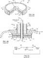
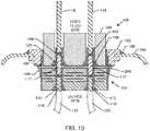
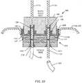
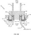
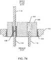
- FIGURE 3Aillustrates an isometric cut away view of a unipolar feedthrough capacitor. Shown, in cut away view, are active electrode plates 134 and ground electrode plates 136 both disposed within a capacitor dielectric 171. There is a feedthrough hole (passageway) 176, including metallization 130. There is also an outside diameter metallization 132.
- FIGURE 3Bshows the unipolar capacitor of FIG. 3A in section, mounted to the ferrule 122 of a hermetic seal subassembly 116 for an active implantable medical device.
- the ferrule 122is configured to be laser welded 128 into an opening of an AIMD housing previously illustrated in FIG. 2 as element 102.
- the AIMD housingis generally of titanium or other biocompatible conductive material and forms an overall electromagnetic shield to help protect AIMD electronics from electromagnetic interference emitters, such as cell phones and the like.
- the ground symbol 144representing that EMI signals that may be coupled onto the body side of the lead 118, can be decoupled or diverted through the feedthrough capacitor 124 to the equipotential shield.
- high frequency electromagnetic signalsare diverted from lead 118 to the AIMD housing 102, they circulate around the shield and are converted into meaningless heat (just a few milli or microwatts).
- FIGURE 3Cis the schematic diagram for the feedthrough capacitor of FIGS. 3A and 3B .
- thisis known as a three-terminal device and that there is significant high frequency attenuation along the length of the leadwire between 118 and 118'. Accordingly, the first terminal is on the body fluid side 118 and the second terminal is on the device side 118', the third terminal being the ground 102,144, where undesirable electromagnetic interference is diverted to the AIMD housing. It is known in the art that three-terminal feedthrough capacitors have very little to no parasitic series inductance and are therefore, very broadband low pass filters.
- FIGURE 3Dis an exploded view of the unipolar capacitor of FIG. 3A showing that it has ceramic cover plates 154, active electrode plates that are interleaved with ground electrode plates 136 and one or more cover sheets disposed on the other end 154.
- the ceramic dielectricswould typically be of BX or X7R having a dielectric constant of approximately 2000 or higher. It will also be appreciated that NP0, which is generally a low k dielectric with a dielectric constant below 200, could also be used, as taught in U.S. Patent 8,855,768 .
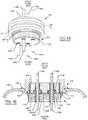
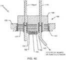
- FIGURE 4Aillustrates a quadpolar feedthrough capacitor and hermetic terminal subassembly 116 where it has four leadwires 118a - 118d and four feedthrough holes (quadpolar). It has a metallic ferrule 122 generally of titanium which is ready for laser welding 128 into the AIMD housing 102 (not shown).
- FIGURE 4Bis a prior art sectional view taken generally from section 4B-4B from FIG. 4A .
- hermetic terminal subassembly leadwires 118a-dpass all the way through the entire structure, namely, the hermetic terminal subassembly 116 and the feedthrough capacitor 124.
- these hermetic terminal subassembly leadwires 118a-dare electrically and mechanically continuous (single material) and pass through from the body fluid side to the inside of the device 100 housing 102.
- hermetic terminal subassembly leadwires 118a-dpass through from the body fluid side to the inside of the device housing by way of header block connector assembly 104 or the like, it is very important that these hermetic terminal subassembly leadwire 118 materials be both biocompatible, biostable and non-toxic.
- these hermetic terminal subassembly leadwiresare constructed of platinum or platinum-iridium, palladium or palladium-iridium, niobium or the like. Platinum-iridium is an ideal choice because it is biocompatible, non-toxic and is also mechanically very strong. The iridium is added to enhance material ductility and to enable the hermetic terminal subassembly leadwire to sustain bending stresses.
- FIGURE 4Cis an electrical schematic representation of the quadpolar filtered feedthrough assembly 116, 124, as previously illustrated in FIGS. 4A and 4B .
- feedthrough capacitor 116, 124has a first terminal 118a, a second active terminal 118'a and a ground terminal 102, 122.
- feedthrough capacitorsare known as broadband low pass filters. They have practically zero series inductance and are desirable in that, they work over a very wide range of frequencies. In general, feedthrough capacitors and their internal electrode geometries are well known in the prior art.
- the feedthrough capacitoris a diverter element, in that, it diverts RF signals on all four leads to the AIMD housing as previously described. This is important for the capacitance reactance formula.
- the capacitor impedanceis extremely high and the capacitor acts like it's not present.
- the capacitortends to look more like a short circuit and diverts those undesirable signals to the AIMD housing.
- U.S. Patents 4,424,551 ; 5,333,095 ; 5,978,204 ; 6,643,903 ; 6,765,779is referred to U.S. Patents 4,424,551 ; 5,333,095 ; 5,978,204 ; 6,643,903 ; 6,765,779 .
- FIGURE 4Dis an exploded view of the quad polar capacitor 132 of FIG. 4A .
- the effective capacitance areacomes from the overlap of the active electrode 134 with the ground electrode 136. The greater this overlap area is, the higher the capacitance of the feedthrough capacitor becomes.
- FIG. 4Dthere are two active and ground plates shown. This has the effect of increasing the capacitor's effective capacitance area. It will be appreciated that as many as 400 or more ground and active layers could be used.
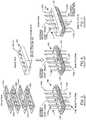
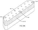
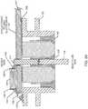
- FIGURES 5, 6 and 7illustrate an internally grounded prior art feedthrough capacitor.
- internally grounded feedthrough capacitorsare known in the prior art with reference to U.S. Patents 5,905,627 ; 6,529,103 ; 6,765,780 and the like.
- FIG. 5one can see an internally grounded feedthrough capacitor, which is octapolar (eight active leads).
- the eight active leadsare labeled 118a through 118h on the body fluid side and on the inside of the AIMD housing they are labeled 118'a through 118'h.
- the ferrule 122has a peninsula structure 139, which is connected to an internal ground pin 118gnd.
- the octapolar feedthrough capacitor active electrode plates 134are designed to overlay in a sandwich fashion the ground electrode plates 136.
- the internal ground lead 118gndis electrically connected to the ground electrode plate layers 136.
- the active electrodes 134a through 134hare each electrically connected through their respective leadwires 118'a through 118'h.
- the overlap between the active electrodes 134 and the ground electrodes 136create what is known as effective capacitance area (or ECA).
- ECAeffective capacitance area
- the active and ground electrode layersmay be interleaved with additional ceramic layers to build up the dielectric thickness (not shown).
- the monolithic ceramic feedthrough capacitor 124is a result of laminating the various electrode layers together and then sintering them at a high temperature to form a rigid monolithic ceramic block.
- Thisis known as a single feedthrough capacitor that is multipolar (in this case these are octapolar or eight active filtered circuits).
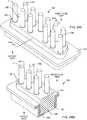
- a perimeter metallization 132on the outside of the round capacitor from FIGS. 3A and 4A whereas, in this case in FIG. 6 , there is no perimeter metallization 132 at all.
- the capacitor 124'is free to float and is therefore, much more resistant to such stresses.
- the internal ground lead 118'gndmakes a low impedance connection from the capacitor's internal electrode plates 136 to the ferrule 122. This is what eliminates the need for the electrical connection material 148, as previously illustrated in FIG. 4 . It will be appreciated that only one ground pin is shown in FIG. 6 , but some designs may require a multiplicity of ground pins spaced apart such that, there is a very low impedance connection effectively grounding the capacitor internal electrodes 136 at multiple points.
- the feedthrough capacitor 124'can also be described as a three-terminal feedthrough capacitor with multiple via holes or feedthrough holes.
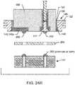
- the hermetic terminal subassembly 189is often referred to in the art as a hermetic feedthrough. Therefore, we have the term feedthrough applying both to the feedthrough capacitor and to the hermetic terminal assembly. As used herein, these are two separate and distinct subassemblies, which are joined together in FIG. 7 to become a feedthrough filter hermetic terminal assembly 116 ready for installation into an opening of an AIMD housing. Referring once again to FIGS.
- leadwires or lead conductors 118', 118are continuous leadwire.
- the leadwireis of the same material as on the device side. This is typical in the prior art.
- the internal ground lead 118'gnddoes not extend through to the body fluid side of the hermetic terminal feedthrough subassembly 189. It will be appreciated that it could be easily and readily extended to the body fluid side, but in most embodiments, it is not necessary.
- hermetic terminal subassembly leadwires 118a-dAn issue with the use of platinum for hermetic terminal subassembly leadwires 118a-d is that platinum has become extremely expensive and may be subject to premature fracture under rigorous processing such as ultrasonic cleaning or application use/misuse, possibly unintentional damaging forces resulting from Twiddler's Syndrome. Accordingly, what is needed is a filtered structure like a feedthrough capacitor assembly 116 which eliminates these high-priced, platinum, platinum-iridium or equivalent noble metal hermetic terminal subassembly leadwires 118. For additional examples of hermetic terminal subassemblies with feedthrough capacitors that employ leadwires 118, one is referred to U.S.
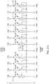
- FIGURE 7Ais the electrical schematic for the feedthrough filtered hermetic terminal 116 previously described in FIGS. 5, 6 and 7 .
- the telemetry pin Twhich passes through the filtered hermetic terminal assembly 116 without any appreciable capacitance to ground. In other words, it would be undesirable to have any high frequency filtering of the telemetry terminal since this would preclude the ability to recover stored information or program the AIMD device remotely.
- Leadwires 118a through 118hall have feedthrough capacitor hermetic terminal assemblies 116, 124 as shown.
- the internal ground pin 118gndis shown only on the device side of the hermetic terminal subassembly 189. Referring once again to FIGS.
- FIGURE 8illustrates the present invention where leadwires 118 on the body fluid side could be directed to a connector block cavity 104, 106 or directly to lead conductors (see FIG. 2 ).
- body fluid side leadwires 118must be of biocompatible, non-toxic and biostable materials. This limits the materials to platinum, palladium, niobium, tantalum, titanium and equivalents or combinations thereof.
- Leadwires 118are co-brazed 138, co-welded 424 or both to short platinum (palladium or the like) pins (leadwires) 117, as illustrated.
- the gold braze 138When the gold braze 138 flows, it forms a strong mechanical and hermetic seal both to the high cost leadwire 118, to the short platinum pin 117 and to the sputtering 150, 152 of the insulator 188.
- the gold braze 138Referring to the left-hand hermetic braze 138, one can see that it is disposed towards the device side of the hermetic seal insulator 188.
- the gold braze 138'extends all the way to the right side of the body fluid side.
- the left-hand side of hermetic seal 138could be moved and disposed on the body fluid side. In this case, the platinum or equivalent solderable pin 117 would have to be extended in length.
- platinum-iridium leads or palladium-iridium leadsis the iridium, at the surface, tends to oxidize making properly wetting these leads with solder (or a thermal-setting conductive adhesive) a problem.
- solderor a thermal-setting conductive adhesive
- the short pin 117not only be very noble (in other words, not oxidize), but also have a very high melting point. This is so it will maintain its structural integrity while the gold braze preform 138 is reflowed in a gold brazing furnace operation.
- the melting point of pure goldis 1064°C.
- the melting point of platinumis 1768°C.
- the melting point of palladiumis 1555°C.
- adhesion layer 152 and a wetting layer 150that have been applied to the inside diameter and outside diameter (or perimeter) of the alumina ceramic insulator 188. These are required because gold preforms generally will not wet or adhere to bare alumina insulators.
- the alumina insulator shown in FIG. 8has been manufactured in a separate manufacturing operation and sintered and fired (as hard as a rock). Through sputtering processes, an adhesion layer 152 is first laid down and then over that, a wetting layer 150 is laid down. This can also be done by some manufacturers in a single process, which combines wetting and adhesion properties into one (such as niobium).
- the embodiment shown throughout this inventionwould be one of applying a silver or palladium-silver bearing glass frit, which is fired on as a single layer 130.
- the metallization 130 or capacitor 124 outside diameter or perimeter metallization 132be shown throughout this invention as a single layer (but as previously mentioned, it could consist of several different layers).
- ceramic feedthrough capacitor metallizations 130, 132can be a metal bearing glass frit or be plated on when the plating operation may consist of selectively plating on one or more under-layers and then a final layer, which would be solderable or receptive through a thermal-setting conductive adhesive 148.
- the machined ferrule 122illustrated in FIG. 8 , could also be replaced by a stamped ferrule or even a two-piece ferrule, as taught in U.S. Patents 8,927,862 ; 9,431,814 ; and 8,604,341 ; and U.S. Patent Publications 2015/0245468 and 2016/0287883 .
- the machined ferrule 122is relatively expensive, not just because of the machining process, but because the machining starts with a solid block of titanium and there is a great deal of scrap produced.
- a stamped metal ferrule or a two-piece stamped ferrulethereby, significantly reduces the machining costs and also results in a material savings, as shown later in FIG. 22 . It will be understood that any of the machined ferrule in this teaching could be replaced with stamped ferrules in accordance with the referenced patents and publications.
- the device side leadwire 118'can now be of very low cost materials, including copper, tin, or the like.
- This leadwire 118'could be a solid wire, can be a stranded wire, can be a braided wire and the like.
- a high cost platinum-iridium or palladium wirewould be in a single piece all the way to the device side to the body fluid side.
- the novel two part co-welded or co-brazed leadwires of the present inventionallow one to then use very low cost leadwires 118' on the inside of the device or the device side, which route a filter feedthrough assembly 116 to device electronics circuits, including a circuit board 126, as previously illustrated in FIG. 2 .
- the advantage of stranded wires or braided wiresis they are generally more resistant to shock and vibration load. Stranded or braided wires are also more flexible and more easily routed to internal circuit boards (not shown).
- the short pins 117could also comprise nickel, in that, nickel has a very high melting point and could accept gold braze 138.
- FIG. 8shows a leadwire/lead conductor 30, which would be routed to an implantable lead conductive in distal electrodes (not shown). This lead is co-brazed 65 to a hermetic seal insulator 90 as shown. There is a feedthrough capacitor 50 illustrated and a nail head structure 60 that also forms a wire bond pad.
- an electrical conductive material 75which could comprise, for example, a solder or a thermal-setting conductive adhesive that connects between the nail head pin structure 60 and the gold braze 65, which is also gold brazed to the body fluid side pin 30.
- an electrical conductive material 75could comprise, for example, a solder or a thermal-setting conductive adhesive that connects between the nail head pin structure 60 and the gold braze 65, which is also gold brazed to the body fluid side pin 30.
- Such a series connectioncan readily compromise the reliability of the overall system if there is shrinkage of the electrical conductive material 65, vibration fractures, micro-cracks or separation of these series elements.
- the present inventionis very different from the Wolf patent, in that, the body fluid side lead 118 is co-welded or co-joined to the device side pin 117. As described in FIG.
- the body fluid side leadwire 118 and the device side pin 118are co-joined by extremely reliable welding or brazing processes. These form a very strong metallurgically reliable bond as well as a very low resistance low impedance electrical connection.
- the present inventionovercomes the difficulties as described in the Wolf patent.
- the electrical connection material 148that connects between the capacitor outside diameter metallization 132 to the gold braze 140 that makes the low impedance (very low resistance) RF diverting circuit to the ferrule 122.
- a non-conductive polymersuch as an epoxy or a polyimide covering 147 disposed over the feedthrough capacitor. This material 147 helps in binding to the low cost leadwires 118 and improves their pull strength.
- the non-conductive epoxy or fill 147provides a pleasing cosmetic appearance.
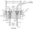
- FIGURE 8Ais very similar to FIG. 8 , except that in this case, the insulator 188 sits on top of the ferrule structure 122.
- the gold braze 140has been wetted between the alumina insulator 188 and the ferrule.
- a direct connection to titaniumis generally undesirable due to the build-up of titanium oxides, which can be resistive or even semi-conductive.
- FIGURE 8Bis very similar to FIG. 8 , except that in this case, there is no gold braze between the insulator 188 and the ferrule 122.
- there is a CERMET material 131which is co-sintered into the ferrule 122 and forms a strong mechanical and hermetic seal between insulator 188 and ferrule 122.
- a CERMET in the artis known as ceramic metal paste, which is then sintered at high temperature and is, after sintering, highly conductive.
- the capacitor electrical connection material 148connects between the capacitor outside diameter or perimeter metallization 132 to at least part of the CERMET 131 so that we do not have a problem with direct contact, only to the titanium ferrule surface 122.
- Conductive via fill materials of alumina/platinum or pure platinumare described, but other materials including Cermets may be used.
- other nonlimiting ceramics, glass ceramics, and/or glass oxidesmay be added to the metal-containing inks/pastes to customize TCE matching/transition pending core material and/or insulator material selections. Palladium may be used instead of platinum.
- Nonlimiting biocompatible metals and alloys that may be used in place of platinuminclude niobium, platinum/palladium, stainless steels, and titanium.
- any of the following list of materialsmay be used alone or combination with any of the materials already discussed or within this list: Gold (Au), silver (Ag), iridium (Ir), rhenium (Re), rhodium (Rh), titanium (Ti), tantalum (Ta), tungsten (W), zirconium (Zr), and vanadium (V), Cobalt Chromium Molybdenum Alloy, Cobalt Chromium Nickel Iron Molybdenum Manganese Alloy, Cobalt Chromium Tungsten Nickel Iron Manganese Foil, Cobalt Nickel Chromium Iron Molybdenum Titanium Alloy, Cobalt Nickel Chromium Iron Molybdenum Tungsten Titanium Alloy, Cobalt Nickel Chromium Molybdenum Alloy, Copper Aluminum Nickel Alloy, Copper Zinc Alloy,
- FIGURE 8Cis very similar to FIGS. 8 , 8A and 8B , except in this case, the ferrule 122 is round. It has a notch 121 for capturing the AIMD housing 102 where a convenient laser weld 128 may be formed.
- the cross-section shown in FIG. 8Ccould be round, as previously illustrated in FIGS. 3A and 4A ; however, it will also be appreciated that the ferrule of FIG. 8C could also be of more of a rectangular shape, as previously illustrated in FIGS. 5, 6 and 7 . Referring once again to FIG. 8C , this shows a round cross-section of the ferrule and if the feedthrough capacitor is also round, then generally the ferrule 122 would form a toroidal or donut shape.
- FIGURE 8Dis very similar to FIG, 8 through 8C , except that in this case, the alumina ceramic 188 has been replaced with a glass seal 191.
- Thismay be a compression glass or a fusion glass, which are well known in the art.
- the novel two-part pin of the present inventionhas been pre-welded 424 (it will also be appreciated that the leads could be pre-co-brazed 138' together before the glass sealing operation instead of welded) so it can be placed into the glass sealing fixture as the glass wets to both the leads and the inside of the ferrule at once forming a mechanical and hermetic seal.
- An optional alumina ceramic or equivalent insulator sheet 193is shown.
- This insulator 193would be placed on top of the glass pre-form prior to the glass sealing process.
- the advantage of having an alumina or equivalent ceramic sheet 193 disposed towards the body fluid sideis that very little of the glass 191 ends up being exposed to body fluids, which can act as solvents.
- the alumina sheet 193makes the assembly of FIG. 8D more stable over the long life of an active implantable medical device.
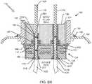
- FIGURE 8Eis similar to FIG. 8 , except that in this case, the diameter or perimeter of a feedthrough capacitor 124 is enlarged. This is often required for high voltage implantable cardiofibrillator devices where the dielectric thickness has to be quite high so the capacitor has a high voltage rating. Accordingly, in order to increase the feedthrough capacitor's effective capacitance area (ECA), it is required to make the capacitor larger in either its length, width or outside diameter. This creates a problem, in that, the capacitor outside diameter metallization 132 no longer aligns with gold braze 140. In this case, a small or separate round or square or other shape gold pad has been co-brazed, which is not part of the hermetic seal 140. This small area of gold braze 141 allows for the capacitor metallization 132 to be electrically connected 148 to a non-oxidized surface and therefore, provide a very low resistivity path to the ferrule 122 to the AIMD electromagnetic shield housing 102.
- ECAeffective capacitance area
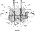
- FIGURE 8Fis similar to FIG. 8 , except that the ferrule structure 122 has been modified such that the capacitor 124 fits partially down into the ferrule.
- Electrical attachment material 148comprises a thermal-setting conductive adhesive, such as a conductive epoxy or a conductive polyimide or a solder or the like. It makes an electrical connection between the capacitor metallization 132 and gold braze 140 as illustrated. Having the capacitor sit down part way into the ferrule allows automatic assembly by dispensing of thermal-setting conductive epoxy or solders by robots.
- U.S. Patent 6,643,903One is referred to U.S. Patent 6,643,903 .
- the capacitor 124is subsequently added.
- the insulator assembly 189is inverted and an optional adhesive insulative washer 206 is placed against it as shown.
- the capacitor 124is disposed on top of the adhesive washer, which is then cured in an elevated temperature. This not only firmly and mechanically attaches the feedthrough capacitor 124 to the hermetic seal subassembly 189, but it also confines the area around the platinum, palladium or alloys thereof pins 117, such that a subsequent soldering operation 410 cannot flow between the capacitor and the insulator, thereby, shorting out from lead to lead or lead to ferrule (ground).
- the electrical connection material 410could also comprise a thermal-setting conductive adhesive, such as a conductive polyimide or conductive epoxy. It's extremely important in the case of use of thermal-setting conductive adhesives, that an insulating washer 206 be used, such that the conductive material, such as silver particles, in the thermal-setting conductive adhesives, do not migrate or short out from pin to pin or from pin to ferrule or from pin to ferrule gold braze 140.
- a low cost insulated (insulation 123 is optional) lead 118'is placed along with a solder preform 410. This is best illustrated in FIG.
- hermetic seal subassembly 189has been inverted and one can see the two platinum, palladium or alloys thereof pins 117 sticking up.
- the insulative washer 206is then disposed over the pins 117 and the feedthrough capacitor 124 is placed adjacent the insulating adhesive washer 206. This is then pre-cured so they are firmly adhered and mechanically bonded together.
- adhesive washer 206it is usually required that a weighting or a spring fixture (not shown) be placed on the top (device side) of the feedthrough capacitor 124. This pushes the feedthrough capacitor firmly against the adhesive washer 206 and the surface of the insulator 188 so that they all bond together.
- solder preform 410is placed into a counter-bore or counter-sink 127 in the device side surface of the feedthrough capacitor.
- a low cost leadwirewhich is typically a tinned-copper leadwire 118', is placed through the solder preform 410.
- the length of the conductive part of this leadwire 118'is chosen so that the low cost tin-copper leadwire will either touch or become very close to the platinum, palladium or alloys thereof pins 117 of the hermetic insulator.
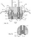
- FIGURE 10illustrates the completed assembly prior to reflowing the solder preform 410.
- FIG. 8increases the reliability of the wiring to the device side of the electronics through lead 118' with its optional insulation 123.
- the reflow solder connection 410not only forms a butt joint between the low cost leadwire 118' and pin 117, but also the solder 410 flows all about both leads 118' and 117, thereby making the electrical connection not only a butt connection, but also a shear connection. It will be known to reliability engineers that solder joints that embody shear stresses will be more resistant to shock vibration, reflow and the like. Shear forces are also set up between the solder 410 and the inside diameter of the capacitor feedthrough hole metallization 130. This double shear increases the mechanical strength of the attachment of the low cost leadwire 118' and also increases its pull strength force. It will also be appreciated that instead of a solder preform 410, one could use a thermal-setting conductive adhesive, such as a conductive epoxy or a conductive polyimide.
- solder (or equivalent material) 410has flowed all about the exposed end portion of the platinum/palladium pin 117 and the low cost leadwire (tin/copper) 118'.
- solderor equivalent material
- the choice of solders for making connection 410are somewhat limited in that, they need to have a relatively high melting temperature. This is because of the subsequent laser welding operation 128 wherein, the ferrule 122 is joined mechanically and hermetically to the AIMD housing 102.
- the laser welding operation 128elevates the entire structure to a fairly high temperature (approximately 260°C).
- solderscontain less than 20-25% Sn as the inventors have found that solders with a higher Sn content become brittle and can induce cracks in the ceramic capacitor body when thermally shocked. Such cracks can result in latent electrical field failures.
- Two example solderswould be AG1.5 or SN10.
- AG1.5is 97.5% Pb, 1% Sn, and 1.5% Ag with the balance being lead and it has a very high melting point, close to 300°C.
- SN10is a composition comprising tin and lead and also has a very high melting point.
- SN10is 88% Pb, 10% Sn and 2% Ag. Solders that contain silver are desirable to prevent leaching of the terminations from the ceramic capacitor.
- the chart shown as FIG. 78details various solder compositions that may be used by one skilled in the art when manufacturing the present invention. This list is not meant to be a full and complete list, but rather shows some of the solder compositions that could be used.
- the body fluid side, low cost leadwire 118can have a gap between it and the short platinum, palladium or alloys thereof pin 117. This gap is shown on the left-hand side of FIG. 8 .
- the body side leadwire 118has been pre-welded 424 to the pin 117. This pre-welding 424 guarantees that the mechanical and electrical connection be very robust, but it also facilitates manufacturing and assembly just prior to the gold brazing operation 138. It is much easier for an operator to drop in a single lead into a carbon boat before it goes into the gold brazing furnace, then two pieces shown as the left-hand side 117, 118 of this figure.
- solder preform 410picks up additional strength, not only because it is in sheer around the circumference of pin 117 and leadwire 118', but it is also wetted to the inside feedthrough capacitor diameter metallization 130. Accordingly, the solder preform 410 not only mates around pin 117 and 118', but it also wets completely to the ceramic capacitor 124 inside diameter of feedthrough hole metallization 130. This creates additional sheer strength.
- solderingcan be accomplished by either reducing or inert gases, thereby eliminating the need for fluxes and also a temperature profile could be created where the relatively fragile ceramic capacitor 124 can be slowly heated up and the solder 410 molten stage can be held to a relatively short amount of time and then the entire assembly is then slowly cooled down. It is desirable not to have the high temperature solder 410 be molten for too long as the capacitor termination material 130 can actually dissolve or leach undesirably into solder 410.
- the ceramic capacitorhas counter-sinks 127 to facilitate placement of the solder preform 410.
- This counter-sinkis best viewed in FIGURE 9 , as element 127. It will also be appreciated that the counter-sink could be replaced by a counter-bore or even a straight through hole as will be further described.
- the hermetic seal 191is now a glass-fused or compression glass seal.
- the hermetic seal 188is typically of alumina, which is gold brazed to the ferrule 122; thereby, forming a hermetic seal 140.
- gold brazes 138 and 138'as previously described in FIG. 8 , which also form a hermetic seal between the alumina or ceramic insulator 188 and both body fluid side leads 118 and device side leads, short lead pins 117.
- FIG. 8Dis a similar structure, except the hermetic seal to the ferrule 122 is accomplished by the sealing glass 191.
- the insulating washer 206could be replaced by a thin ceramic, such as an alumina washer.
- alumina washer 193disposed on top of the glass seal 191. The reason for the alumina washer 193 is that, the glass seal would bond very tightly to it; thereby, adding to the overall strength and hermeticity of the package.
- a fusion or a compression glass 191there could also be a number of ceramic glasses that could be used.
- FIG. 8Done will see that there is a gold braze area 141 that can be continuous or discontinuous or only in spots on top or on the device side of the ferrule 122.
- Thisprovides an oxide-free electrical connection surface to which electrical connection material 148 forms a low impedance connection between the ferrule and the outside diameter or perimeter metallization 132 of the feedthrough capacitor 124. Problems associated with this are described by U.S. Patent 6,765,779 ; 9,108,066 ; 9,427,596 (oxide-free metal addition).
- the oxide-free material 141would be a gold braze.
- the reference patentsalso show that a number of other oxide resistant materials could be used to perfect a low impedance electrical connection between the capacitor outside diameter perimeter metallization 132 and ferrule 122.
- the hermetic terminal subassemblyby focusing only on the bottom portion 189, which is the hermetic terminal subassembly, one can see that when the gold braze 138 is placed through gravitational and capillary action in the gold braze furnace, it will flow down and form the gold braze hermetic seal joint 138. It is important that this hermetic seal joint 138 encapsulate both the short pin 117 and the body fluid side leadwire 118.
- the hermetic seal subassembly 189has been inverted. Since the gold braze joints 138 and 140 have been formed at very high temperature, they will not be disturbed nor will they reflow during the subsequent capacitor 124 soldering operation 410.
- the hermetic terminal subassembly 189is manufactured in an entirely different manufacturing line with a different set of controls, including braze furnaces and the like. It is equally important to note that the feedthrough capacitor assembly 124 is generally performed in an entirely different manufacturing line (usually in Class 10,000 or better clean rooms). It is a monolithic device consisting of alternating layers of ground and active electrodes, which goes through a number of binder bake-out and then sintering operations. Subsequent to that, metallization layers 130 and outside diameter metallization layer 132 are applied, either by electroplating, by applying conductive glass frits (and firing) and the like. In the final operation shown in FIG. 9 , the capacitor subassembly 124 is adhered 206 to the hermetic terminal subassembly 189 and at the same time, device-side leadwires 118' are co-joined.
- the electrical attachment materialwould be a thermally-conductive polyimide, which is cured around 290 to 300°C, but can withstand short-term temperatures up to 500°C. So in this case, the capacitor diameter or perimeter electrical connection 148 would first be formed and then the solder preform 410 would subsequently be reflowed at around 300°C.
- the hermetic seal subassembly 189at the bottom is the hermetic seal subassembly 189. This also appears inverted in FIG. 8 with the capacitor 124 attached to it.
- the short pins 117could, of course, be of platinum or palladium as described, but also could be of a variety of other materials. It should be noted that these short pins 117 are never exposed directly to body fluid and therefore, they do not need to be biocompatible or non-toxic. For example, pins 117 could be of nickel. If the pins were of nickel, they could still be co-gold brazed 138 to the body fluid side leadwires 118.
- nickel leadwires or the likewere either tinned, solder, flowed or electro-plated etched and then tin-dipped or electroplated, for example, with gold or a gold flash to facilitate solderability. This could easily be achieved in a subsequent operation after building the hermetic seal subassembly as illustrated as 189.
- Another optionwould be to sputter a layer of gold, for example, or platinum onto the exposed ends of the pins 117 to facilitate solderability.
- the body fluid side leadwires 118'have a first end 341 that will at least be partially disposed within the passageway of the feedthrough filter capacitor while the second end 342 will be disposed past the feedthrough filter capacitor configured to be connectable to electronics internal to the AIMD.
- FIGURE 10illustrates the capacitor 124 co-joined to the hermetic seal subassembly 189 by adhesive washer 206.
- the device side leads 118'have been placed through their solder preforms 410.
- FIG. 10illustrates the entire assembly 116 just prior to reflow of the solder preform 410. After the solder preform 410 is reflowed at an elevated temperature, it will result in the structure 189, as illustrated in FIG. 8 (inverted). As can be seen, the solder preform 410 flows all around the two pins 117, 118'.
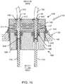
- FIGURE 11is very similar to FIG. 8 except on the capacitor device side, counter-bores 135 are shown instead of counter-sinks 127.
- the right side of the devicenow has a wire bond pad 131 which may be proud of the feedthrough capacitor 124.
- This nail head 131may be proud of the device side surface of the feedthrough capacitor 124 (as shown) or it may be flush with the surface (not shown), or it may be reduced below the surface (not shown).
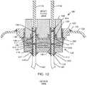
- FIGURE 12is very similar to FIG. 8 , except that the counter-sinks 127 have been eliminated on both the right and the left side of the device side of the feedthrough capacitor 124. This will make it more difficult to place a solder preform 410 and have it reflow properly.
- counter-bores, counter-sinks or combination and variations thereofcan be used, or alternatively, as shown in FIG. 12 no such structures are used to help locate and place the solder preform 410.
- the feedthrough capacitor inside diameter (or via hole) metallization 130has been extended 411 onto the device side of the feedthrough capacitor 124 such that it forms a circular portion, which is also known in the industry as a white-wall tire shape.
- this metallization 130, 411can be mechanically and electrically adhered to the capacitor electrode plates by firing a silver or palladium-silver glass frit, electroplating or the like. In all cases, the metallization 130, 411 firmly adheres to the body of the feedthrough capacitor 124.
- the presence of the white-wall tire metallization 411allows for the solder 410 to form a fillet 410' between the lead conductor 118' and metallization band 411.
- FIGURE 13is very similar to FIG. 8 , except that in this case, the counter-bores on the device side of the hermetic insulator 188 have been replaced by counter-sinks 133.
- FIGURE 14is very similar to FIG. 8 , except that the counter-bores 129 in the alumina ceramic insulator 188 have been removed. This will make it more difficult to place gold brazed preforms 138 (not shown before brazing). Again, it will be understood by one skilled in the art that counter-bores, counter-sinks or combination and variations thereof can be used, or alternatively, as shown in FIG. 14 no such structures are used in the insulator 188 to help locate and place the gold brazed preforms 138 (not shown before brazing).
- FIGURE 15is very similar to FIG. 8 , except that the body fluid side leadwires 118 have been replaced by biostable and biocompatible wire bond pads 133. In a preferred embodiment, these pads are drawn from a single piece of wire 118, which extends down into the gold braze 138.
- FIGURE 16illustrates an alternate method of manufacturing a nail-headed lead 118 as previously described in FIG. 15 .
- FIG. 16illustrates that the nail head 412 may be machined as a separate structure and then gold brazed 422 to the lead 118.
- Gold braze 422would typically be a co-brazing operation at the same time gold brazes 138 and 140 are formed.
- sputter layers 150,152are not shown for simplicity.
- FIGURE 17illustrates that the nail head 410 may be modified to have an elongated piece that engages the gold braze preform. This aids in centering and aligning the nail head 412 with the lead 118.
- FIGURE 18one can see that a counter-bore may be included within the machine nail head 412 into which the lead 118 protrudes. Again, this helps with alignment during the gold braze flowing operation 422.
- FIGURE 19is very similar to FIG. 18 , except that in this case, the counter-bore and nail head 412 is smaller and that a protrusion or extension is formed on the end of lead 118 to engage counter-bore 418. Again, this is to help with maintaining alignment during the gold braze reflow operation 422.
- FIGURE 20illustrates that the nail head 412 may have a semi-circular (or other) shape.
- the advantage of the semi-circular shapeis that this increases the wetting and sheer area to the gold braze 422 and also increases the gold braze contact area to the lead 118. This contact area can be further increased by using a larger gold preform 422, as illustrated in FIGURE 21 .
- a weighting fixture(not shown) may be applied to the top of any of the nail heads or even an alignment fixture so that they are properly held in place during the gold braze reflow 422.
- FIGURE 22is very similar to FIG. 8 , except that the ferrule structure 122 has been completely eliminated. By eliminating the ferrule, one eliminates a significant amount of cost. Typically, these titanium ferrules are machined out of a solid piece of titanium, which entails a substantial amount of machining time, labor and scrap. Referring to FIG. 22 , one can see that the AIMD housing 102 has been bent down to form an aperture 428 into which the hermetic seal insulator 188 is aligned. The insulator 188 is then gold brazed 140 directly to the AIMD housing 102. This is actually co-brazed along with gold braze 138 as previously described.
- the gold braze 140may be done to a lid or a shield assembly, which is subsequently laser welded into the AIMD housing 102 (not shown).
- a lid or a shield assemblywhich is subsequently laser welded into the AIMD housing 102 (not shown).
- the length of leadwire 118'can be of any suitable length to reach a circuit board or even provide for a stress-relieving or strain-relieving loop.
- the insulation 123 on the right side of FIG. 22can be an insulation sleeve, an insulation tubing or even a heat-shrink tubing, which is added later.
- a preferred materialwould be an insulative tubing consisting of KAPTON.
- FIGURE 23is the same as FIG. 8 , except that the low cost leadwires 118', instead of being stranded, are solid wire stubs.
- the lengths of these leadwire stubs 118'vary in length below the feedthrough capacitor 124 in accordance with the application. For example, if the customer was going to install a very thin flex cable to make the connection between leadwires 118' and a circuit board 126 (not shown), then the leadwires 118' need not stick out very far. However, if a circuit board was being placed adjacent the feedthrough capacitor 124 with via holes (not shown), then it might be necessary to make the leadwire stubs 118' a little longer.
- FIGURE 24seems similar to FIG. 8 , but it also incorporates all the important advantages previously described for internally grounded capacitors shown in FIGS. 5, 6, 7 and 7A .
- an internal ground pin 118gndwas provided by co-brazing it into a peninsula 139 of ferrule 122.
- a gold braze moat 138, 140, 408is provided, wherein the brazes 138 and 140 are connected by the braze moat 408.
- this gold braze moatcould have the very same appearance as a peninsula 139 as previously described in FIG. 6 .
- this peninsulacould have rounded or square edges or the like.
- a ground lead provided to the header blockcould be a very convenient way of dissipating energy from an abandoned lead or a defective lead.
- U.S. Patent Publication 2014/0243944entitled HEADER BLOCK FOR AN AIMD WITH AN ABANDONED LEAD CONNECTOR CAVITY.
- the feedthrough capacitor 124 of FIG. 24is internally grounded, as previously described in FIGS. 5, 6 and 7 . It also has all of the intended advantages previously described in FIGS. 5, 6 and 7 . Referring to FIG. 8 , one can see that the capacitor outside diameter metallization 132 has been completely eliminated.
- the capacitor outside diameter or perimeter electrical connection 148 to the ferrulehas also been completely eliminated. As previously described, not only does this reduce many expensive manufacturing operations and eliminate expensive materials, but it also allows the capacitor body 124 to mechanically float from the ferrule 122. This is important during subsequent customer laser welding 128 of the filtered feedthrough subassembly 189 into the AIMD housing 102 as illustrated in FIG. 8 .
- the capacitor 124will be much less sensitive to the heat pulse (thermal shock) created by this laser welding 128 since it is not thermally isolated and also mechanically isolated. In other words, there are mismatches in the thermal coefficient of expansion of the ferrule 122 and the ceramic dielectric 124 itself.
- the insulative washer 206is preferably a thin washer, which is somewhat flexible; thereby, mechanically isolating the capacitor even further.
- the insulative washer 206would comprise an adhesive washer of polyimide. Polyimides form ring molecules, which are very stress absorbing as opposed to epoxies, which form very long chain molecules. Accordingly, a polyimide washer 206 would be very stress absorbing.
- a low cost ground leadwire 118'gndwhich is routed to a circuit board (not shown). This ground wire 118'gnd is optional, but does provide a very convenient way of providing an AIMD housing ground 102 for the circuit board electronics.
- hermetic seal terminal subassembly 189 and the corresponding internally grounded feedthrough capacitorare long and rectangular (for example, a 12-pin device)
- multiple ground pins 117gndwould be required. This would result in multiple peninsulas 138, 140, 408 that accomplish a low impedance electrical grounding of pin 117gnd to ferrule 122.
- Each one of these multiple locationscould be associated with a device side low cost ground lead 118'gnd, however, typically, only one such wire 118'gnd is required to connect to a circuit board ground trace (not shown).
- a robotcan place the adhesive washer 206 over the short pins 117 and a robot can also place the feedthrough capacitor 124.
- the solder preforms 410could either be threaded by robot or by hand over leadwires 118' or then inserted into the feedthrough capacitor via holes as shown. Then either a conveyor belt or a batch process is used to reflow the solder preform without the need for repetitive processes. It has been found through experimentation that the manufacturing yield of the product, as illustrated in FIG. 24 , is in the high 99% range. This is an increase in manufacturing yield of greater than 5% compared to the prior art technology illustrated in FIGS. 4A and 4B . Another important advantage that is not really apparent from FIG. 24 is that it is completely and easily reworkable.
- the most expensive subcomponent in FIG. 24is the hermetic seal subassembly 189. It has gold brazes, which are expensive; sputtering, which is expensive: and an alumina insulator, which is expensive. In addition, the ferrule itself 122 tends to be very expensive. It is common practice after the subassembly 116 is formed to do extensive thermal, mechanical and electrical testing before this subassembly 116 is shipped to a customer for installation into an AIMD housing 102. This includes elevated temperature voltage application otherwise known as burn-in and the like. There is usually some infant mortality in the capacitor population 124', meaning that there is a yield associated with this high reliability electrical and mechanical pre-screening.
- the capacitor 124does fail electrically or fails one of its insulation resistance tests, it is easily removable by simply heating it up. In other words, all one has to do is reflow the solder preform 410 and then remove the capacitor from the insulative washer 206 and simply install a new feedthrough capacitor and reuse the hermetic seal subassembly. This is an enormous advantage of the present invention.
- FIGURE 24Ais one possible schematic diagram of the filtered feedthrough assembly 116 of FIG. 24 .
- the ground pin 118'gndextends from the body fluid side all the way to the device side.
- any number of active leadwires 118'are possible from monopolar to bipolar to tripolar ... all the way to "n" number of active leads.
- the telemetry pin Tis optional or may even embody a multiplicity of RF telemetry pins T. In general, the telemetry pin or telemetry pins are not associated with a feedthrough capacitor active electrode 116, 124.
- FIGURE 24Bis almost the same as FIG. 24 , except the body fluid side ground lead 118gnd has been eliminated. In most AIMD applications, it is not necessary to provide an implanted lead conductor that has the same potential as the AIMD housing 102. Referring once again to FIG. 24B , one can see that the gold braze preform 138, 140, 408 has covered the top on the body fluid side of the short lead pin 117gnd. Referring once again to FIG. 24B , one can see that the schematic previously described in FIG. 7A could apply. Referring to FIG. 7A , one notes that the device side ground pin 118gnd does not extend to the body fluid side. Again, any number of active pins are possible and the telemetry pin is optional.
- FIGURE 24Cillustrates a green ceramic bar 188 illustrating that four hermetic insulators are disposed on the bar. It will be appreciated that larger bars may include many more insulators, such as 10, 100 or "n" insulators. Referrring once again to FIG. 24C , one can see that in the green bar there are holes 402 that are formed by drilling, punching or equipment operations. There is also a mil-slot 403 as indicated. It should be stated that a green bar includes the alumina ceramic and binders and solvents. The green bar is easily handled, molded, machined, etc. If one were to grasp the bar of FIG. 24C , one could flex it back and forth somewhat. Prior to sintering, it's important to remove the four separate insulator structures, as will be further explained.
- FIGURE 24Dillustrates the top view of the device side of the bar of FIG. 24C .
- FIGURE 24Eillustrates the opposite side of the green bar of FIG. 24C .
- the shallow slots 403do not appear on the body fluid side.
- FIGURE 24Fis taken from section 24F-24F from FIG. 24D illustrating the slot 403 in cross-section.
- the slot 403becomes a very important and low cost way of providing for internal ground connection to an internally grounded feedthrough capacitor.
- FIGURE 24Gis taken from section 24G-24G from FIG. 24D illustrating the cross-section of one of the holes 402.
- FIGURE 24Hillustrates the green bar of FIG. 24C with a mil-punched or cut braceway 404. This shows each one of the four hermetic seal insulators about to be cut out of the overall green bar 400.
- FIG. 24Hwe now have four separate individual insulators that are ready for sintering.
- sintering of these alumina ceramic insulatorswould be accomplished by a binder bake-out in which the temperatures are fully raised until solvents and binders are released and then the sintering process causes the green alumina ceramic to become fired into a hard, monolithic structure.
- alumina ceramic insulators for human implant applicationshave to be of very high purity so that they can withstand exposure on the body fluid side. Purities of >99% alumina are typical in the industry. Referring back to FIG. 24H , the four insulators are shown for illustration purposes only. It will be appreciated that the bars 400 can be of any size and contain any number of insulators.
- FIGURE 24Iillustrates one of the four insulators of FIG. 24H after it's been sintered and sputtered.
- Sputter layers 150 and 152include a wetting and an adhesion layer such that the alumina insulator 188 will accept a gold braze.
- the inside of the twelve through-holes 186have also been metallized. Referring back to FIG. 24I , the body fluid side is directed upward.
- FIGURE 24Jillustrates the same insulator as FIG. 24I , except in this case, the device side is oriented upward. Importantly, one can see that the slot 403 has also been sputtered or metallized with wetting and adhesion layers 150,152.
- FIGURE 24Kis very similar to FIG. 24J , but illustrates that more than one slot can be used.
- FIG. 24Kthere are three novel sputter slots 403, 403' and 403".
- Filter design engineers familiar with internally grounded capacitorswill appreciate that it is important to have a ground location relatively close to the active pins or active via holes 186. If one of these holes gets too far from ground, the insertion loss with filter performance will be compromised. Accordingly, it will be appreciated that any number of ground points 403 or ground slots 403 can be provided up to "n" number of ground points.
- FIGURE 24Lillustrates the insulator structures illustrated in FIG. 24I and FIG. 24J , placed into, partially within or onto a ferrule 122.
- a gold braze pre-form 140, 140sis added around the perimeter of the insulator and gold braze pre-forms 148 are also placed around each of the body fluid side leadwires T and 118A through 118K. In this case, there is a telemetry pin T that will not be filtered and all of the active leadwires 118A through 118K will be filtered.
- FIGURE 24Mis a sectional view taken from section 24M-24M from FIG. 24L illustrating the grounding slot 140s in cross-section which comprises a gold braze.
- the rest of the insulator perimeter gold brazeis formed to ferrule 122.
- Sputter layers 150 and 152have been omitted for clarity, but will be appreciated that they would be present.
- This gold braze 140, 140sforms relatively mechanically robust and hermetic seal between the ferrule and the insulator 188.
- gold braze pre-form 138 around each of the leadsform a strong mechanical and hermetic seal between the insulator 188 and each of the leads T,118.
- FIGURE 24Nillustrates the hermetic seal subassembly 189 of FIG. 24 inverted and rotated.
- the telemetry pincan also optionally be a two-part pin in accordance with the present invention.
- FIG. 24None can see the top view of the gold braze pedestal slot 140s.
- FIG. 6one can see the prior art machined pedestal 139 for convenient attachment of an internally grounded capacitor 124.
- the gold brazed slot 140swill contact the internally grounded capacitor internal electrode plates.
- the novel gold braze slotprovides a much lower cost convenient alternative to providing a pedestal 139 as previously illustrated in FIG. 6 .
- a dashed line 401that separates the gold braze in the slot 140s from the perimeter gold braze 140.
- the inventorshave found that when one attempts to gold braze both the slot and the full perimeter of the hermetic seal at the same time that gold may flow out of the slot area to where it gets too thin.
- a two-step processmay be used wherein, a pure gold or a higher temperature gold braze is first formed 140 and then in a subsequent gold brazing operation, a lower temperature gold braze or even a lower temperature braze of other materials, like CuSil or TiCuSil, can be placed into the slot area 140f.
- These materialsneed not be biocompatible since they are on the device side not the body fluid side. The important thing is that they be highly conductive and resistant to oxides.
- FIGURE 24Ois a sectional view taken from section 240-240 from FIG. 24N illustrating the novel grounding slot 140s in cross-section.
- FIGURE 24Pillustrates an internally grounded capacitor 124' mounted to the hermetic seal subassembly previously illustrated in FIGS. 24N and 24O .
- the active electrode plates 124 of the internally grounded capacitor 124'are connected to the via hole metallization 130.
- the ground electrode plates 136are connected to the ground via hole metallization 130G which is electrically connected to the internally grounded capacitor's ground electrode plate set 136. It is important to note that the ground electrode plate set for internally grounded capacitor does not extend to the outside perimeter or diameter of the capacitor 124'. Instead, the internal grounding is by a BGA, solder or thermal-setting conductive adhesive connection 202 directly to the gold braze slot 140s as shown.
- the gold braze slot 140smakes a very mechanically robust, but more importantly, a very low resistance connection to the titanium ferrule 122. As previously mentioned, it is important to have connection to a non-oxidized surface. Titanium, such as the titanium of ferrule 122, can form oxides, which can be resistive or semi-conductive. The gold braze 140 burns through these oxides accomplishing a very low impedance electrical connection to the capacitor's ground electrode plates 136. As previously described, depending on the number of active pins and their spacing, a number of novel gold braze slots 140s could be provided, including 'n' number slots as provided as previously illustrated in FIG>24K elements 403. It should be noted that FIG. 24P is a cross-section taken generally through the insulator of FIG.
- a device side, very low cost leadwire 118'gndcan be co-connected or co-soldered at the same time that the electrical connection 202 is made.
- the active lead 118,118'there is a two-part pin consisting of 118 and 117.
- the novel co-brazed or co-welded short pin 117platinum, palladium or nickel or the like
- the novel co-brazed or co-welded short pin 117is shown flush with the insulator surface, such that an electrical connection 202 can be made, as previously described for the ground connection side including attachment of a device side ground leadwire 118'gnd.
- the active pins or active leadwires 118'which will be routed to AIMD electronic circuits or circuit boards, not illustrated.
- On the body fluid sidein general, there is not a need for a ground pin. So on the body fluid side, as previously described in FIG. 24N , there is a telemetry pin T along with active pins 117a through 117k. Each of these active pins are associated with its own active electrode plates, as previously described in FIG. 5 .
- the hermetic seal subassembly, including the internally grounded feedthrough capacitor 124'has been laser welded 128 into the housing 102 of an active implantable medical device.
- the feedthrough capacitor 124is disposed on the device side, which means that it is contained within the hermetically sealed and overall electromagnetically sealed AIMD housing 102.
- the conventional feedthrough capacitor 124has an external metallization or perimeter metallization 132 and a corresponding electrical connection 148. Both of these elements 132 and 148 have been eliminated in FIG. 24P . Elimination of these connections has many advantages, including protection of the relatively sensitive feedthrough capacitor 124' from thermal shocks imposed by laser welding 128 of the completed assembly of the housing of an AIMD.
- FIGURE 24Qis taken from section 24Q-24Q from FIG. 24P illustrating a blow-up of the internally grounded capacitor's ground connection to the gold braze grounding slot 140s.
- the BGA materialwhich can be, of course, of solder or of thermal-setting conductive material, has been reflowed such that it makes a strong mechanical and electrical connection both to the gold braze slot 140s and to the device side ground leadwire 118'gnd.
- the low cost leadwire on the device side 118'gndwill have a very high pull strength since much of the electrical connection material 202 is in shear both to the lead 118'gnd and to metallization surface 130. Also, in this section one can see that the ground leadwire 118'gnd has a tinned surface 115, which helps material 202 flow thereby increasing pull strength and reliability.
- FIGURE 24Ris an exploded view taken from FIG. 24P illustrating that the BGA connection 202 may be dispensed by a robot or by human hand on the hermetically sealed insulator 189 or alternatively to the internally grounded feedthrough capacitor 124' or in some embodiments, to both. Shown is an adhesive insulating washer 206. It will be appreciated that these elements will be brought together and co-attached in a high temperature process which bonds in the adhesive of washer 206 and either subsequently or at the same time, reflows solder BGA connection 202 or thermal-setting conductive adhesive or cures thermal-setting conductive adhesive 202.
- FIGURE 24S and FIGURE 24Tare very similar to FIGS. 24P and 24R , except in this case, instead of a gold braze slot 140s, a peninsula structure 139 is very similar to that described in FIG. 6 , is shown.
- This peninsula structure 139would generally be machined out of the same block of titanium that also forms the ferrule 122. As had been previously described, titanium can form oxides or even tri-oxides, which can be very resistive. Connecting to titanium could preclude the proper insertion loss (filter performance) of the feedthrough capacitor 124'. Referring once again to FIG. 24S , one can see that there is a novel counter-bore 139g into which a gold braze preform 180d is placed.
- gold brazed preform 140dwould comprise a small dot, a rectangle, a slot or any other shape.
- Gold braze preform 140dwould generally be reflowed in a gold braze furnace at the same time that the insulator 188 gold braze to ferrule 140 is formed and also gold braze 138, which hermetically seals and co-joins device side leadwire 186 to pin 117.
- bold braze 140dprovides a non-oxidized surface to which the ground electrical material 202 can be attached.
- the capacitor metallizationon the left side, has been extended onto a portion of the top of the device side of the feedthrough capacitor 119'. This is also known as a white-wall tire effect and when a leadwire (not shown) is added, this greatly increases the pull strength.
- the capacitor via holehas been completely filled with metallization, including a metallization area on the device side of the feedthrough capacitor 119". This provides a convenient location for soldering, for wire bonding of a ribbon or a round lead 118' that will be routed to AIMD electronics (not shown).
- FIGURE 24Uis the schematic diagram of the internally grounded capacitor which was developed all the way from FIG. 24C all the way inclusive to FIG. 24T .
- FIGURE 25illustrates an internally grounded feedthrough capacitor 124' as previously described in FIG. 24 , except that the gold braze moat 138, 140, 408 has been eliminated and instead replaced by internal ground plates 137 that are embedded within a multilayer and co-fired alumina ceramic insulator 188. Sputtering of the adhesion 152 and wetting layers 150 electrically connects these embedded ground plates 137 in parallel. Subsequent gold brazing operation 140 electrically connects the ferrule 122 by way of this sputtering 150, 152 to the ground plates 137. Embedded ground plates within a hermetic insulator are described by U.S. Patent 7,035,076 . Accordingly, the internally grounded structure illustrated in FIG. 25 has all of the advantages previously described for FIG. 24 .
- FIGURE 26illustrates the assembly steps for the structure of FIG. 25 in a manner very similar to that previously described in FIG. 24R .
- a major advantageis the elimination of the capacitor outside diameter or perimeter metallization 132 and electrical attachment 148 to the ferrule (reference FIG. 8 electrical attachment material 148). Accordingly, FIG. 26 is completely designed for automation.
- FIGURE 26is the assembly of FIG. 25 showing it exploded into its various subcomponents. Shown is the internally grounded hermetic insulator subassembly 189 and the internally grounded feedthrough capacitor 124' ready to be disposed on top of the adhesive washer 206 and on top of the hermetic seal insulator 188. As previously described, this assembly can be automated and can be reflowed in a conveyor belt, furnace process or in a bulk process, such as a DAP sealer.
- FIGURE 27illustrates the exploded components of FIG. 26 after the capacitor 124' has been adhesively bonded 206 to the hermetic seal insulator 189 and ferrule 122. Solder preform 410 is in place and ready to be reflowed. Attention should be drawn to another very important advantage of the present invention. This can be seen in FIG. 27 as the diameter or the dimension of a rectangle 125. By elimination of any electrical connection between the capacitor outside diameter or perimeter to the ferrule 122, the capacitor 124' can actually be made larger in diameter or in a rectangular dimension. This adds enormously to the capacitor's effective capacitance area (ECA). It should be noted that this ECA is a square law.
- FIGURE 28is another internally grounded capacitor 124 similar to those previously described in FIG. 24 and FIG. 25 .
- the advantage of FIG. 28is that the gold braze moat 138, 140s, 408 of FIG. 24 has been largely replaced with a metallic piece 141 illustrated isometrically in FIGURE 29 .
- This metallic piece 141would typically be of titanium so that it will readily accept gold brazes 138 and 140s.
- the advantage of using a titanium metallic piece 141is that less gold is required and of course, gold is very expensive. It will be noted in FIG. 28 that in the area where the metal piece 141 is located, sputter layers 150 and 152 cover this peninsula area of the hermetic insulator 188.
- the gold braze layer 138would merge with the gold braze layer 140 as a very thin line of gold above the metal piece 141. This is desirable since it enhances the mechanical, structural and hermetic stability of the entire package. It will be understood that this thin layer of gold will typically be present, but is not shown for simplicity. It is also likely or even probable that the thin layer of gold will partially or totally cover both the top and bottom of the metal piece 141.
- FIGURE 29is a perspective view of the metallic piece from FIG. 28 .
- thisappears to be a machined piece of material, which would typically be of titanium.
- the metallic piece 141could also be a very thin stamped titanium metal which would make it much less expensive to manufacture.
- the stamped or machined metal piece 141 of FIG. 29offers many advantages over the gold brazed slot 140s illustrated in FIG. 24P . It is very difficult to maintain gold braze is it will want to wet or flow to other areas, for example, around the outside diameter or perimeter of insulator 188.
- the metal piece 141prevents the gold from flowing to areas where it is not desired, achieving the result shown in FIG. 28 .
- FIGURE 30is another internally grounded capacitor version.
- the ferrule 122has been extended into a peninsula 139 as shown.
- the ferrule 122would be machined such that, the peninsula 139 is formed.
- peninsula 139could be very similar in shape.
- FIG. 30one can see that there is a short ground pin in accordance with the present invention 117gnd that has been gold brazed 138 into the peninsula 139. This provides a convenient grounding pin for contact to the internally grounded feedthrough capacitor 124 and to ground electrode plates 136.
- the device side of the internally grounded feedthrough capacitor 124'has been provided with convenient counter-sinks for placement of solder preform or thermal-setting conductive adhesives 410. It will be appreciated that one could machine, in one piece, the ferrule 122, the pedestal 139 and the ground pin 117gnd. This would eliminate the ground pin 117gnd and the gold braze 138g. However, now we'd be faced with a problem when the ground pin 117gnd would comprise titanium because it would oxidize. This would require a supplemental plating or sputtering operations, such that one could make a good electrical connection 410 to ground pin 117gnd.
- FIGURE 30Ais similar to FIG. 40 , except that the device side leads 117 and 117gnd have been extended below the surface of an internally grounded feedthrough capacitor 124', such that a flex cable 151 can be attached.
- the flex cable 151can have many different circuit traces. In this case, only two are illustrated for simplicity. These are circuit traces 155 and 157.
- flex cable 151circuit traces 155 and 157 is associated with a via hole for placement over pins 117 and 117gnd and subsequent soldering 153.
- flex cablescan be multilayer or quite wide and have many different circuit traces embedded within them. Flex cables are commonly used in AIMDs for connection to an AIMD circuit board (not shown). Flex cables are also advantageous since their installation can be automated and that they are inherently resistant to shock and vibration stresses.
- FIGURE 30Bis similar to FIG. 30A , except that in this case, leadwires 117gnd and 117 have been elongated such that they can be routed all the way to an AIMD circuit board (not shown).
- leadwires 117 of the present inventionare generally co-brazed 138 or co-welded 424to a device side lead 118, they must be capable of withstanding these high temperature operations.
- a low cost device side leadwire 117comprised of a low melting material, such as copper or the like.
- a suitable materialwould be nickel, which would probably require a supplemental tin dipping, solder coating or plating operation.
- FIGURE 31illustrates a prior art monolithic ceramic capacitor 194. These are otherwise known as MLCCs. Monolithic ceramic capacitors are very well known in the prior art and are produced daily in the hundreds of millions. It will be appreciated that MLCCs are also commonly referred to as multilayer ceramic capacitors. MLCCs are common components in every electronic device, including computers, modern smart phones and the like. It should be noted here that not all rectangular 2-terminal capacitors, as illustrated in FIG. 31 , must be ceramic. As used herein, MLCC or monolithic ceramic capacitors shall also include all kinds of stacked tantalum, stacked film and other dielectric type capacitors that form 2-terminal rectangular shapes. It will also be appreciated that any of the 2-terminal capacitors in the art, including ceramic, film and tantalum could also have other shapes other than rectangular, including cylindrical and the like.
- FIGURE 32taken from section 32-32 from FIG. 31 , illustrates a cross-section of an MLCC capacitor.
- the prior art MLCCis a two-terminal device having a metallization on the left 130 and a metallization on the right 132. It has overlapping electrodes as illustrated in FIGURES 33 and 34 . It has an effective capacitance area ECA created by the overlap of the left-hand electrodes 134 with the right-hand electrodes 136.
- FIGURES 35 , 35A and 35Billustrate prior applications of MLCC capacitors 194 to hermetic seal subassemblies of active implantable medical devices. These patents include: U.S. 5,650,759 ; 5,896,267 ; 5,959,829 and 5,973,906 .
- FIGURE 35Cillustrates a prior art flat-thru capacitor. This is better understood by referring to its internal electrode plates as illustrated in FIGURE 35D . This is also known as a three-terminal capacitor because there is a circuit current i 1 that passes through its electrode plate 175 from the first terminal 180. If there is a high frequency electromagnetic interference signal being conducted along this electrode plate, then it comes out the other side at a second terminal 182. Referring back to FIG. 35C , there is a general disadvantage to such capacitors in that, at very high frequency EMI 188 can cross-couple from the left side of the MLCC capacitor to the right side.
- FIGURE 35E, 35F and 35Gillustrate a three-terminal capacitor that is also known in the industry as X2Y attenuator. These are well known in the prior art. It will be appreciated by one skilled in the art, that any of these flat-thru or X2Y attenuators can be applied to the present invention.
- FIGURE 36illustrates the application of MLCC capacitors 194 and 194' to the present invention.
- the left-hand device side pin 117ais relatively short to accommodate placement of flex cable (not shown) or a circuit board adjacent the hermetic seal insulator 188 and ferrule 122 on the device side.
- the right-hand device-side leadwire 117bhas been elongated so that it can be directly connected to an AIMD circuit board 126 (not shown).
- An optional insulating sleevecould be placed over the right-hand leadwire 117b.
- a disadvantage of MLCC chip capacitorsis that they are two terminal devices and have substantial series inductance.
- MLCC capacitorsbecome increasingly less effective as a filtering element. Accordingly, it is preferable that MLCC chip capacitors be relatively small in size.
- Reverse geometryis a popular technique, where the terminations are placed along the long sides instead of the short sides. Reverse geometry reduces the internal inductance of the MLCC capacitors 194. The advantage of reverse geometry MLCCs for higher frequency filtering is further explained in U.S. Patent Publication 2014/0168917 (look at FIGS. 16 through 18 ).
- the capacitors 194, 194' of FIG. 36have been placed immediately adjacent leadwires 117a and 117b at the point of entry of the AIMD housing.
- MLCC capacitorsdo not have a polarity; therefore, they can be oriented in any direction.
- the capacitor termination 132will also be known as the ground termination. This is because there is an electrical connection 143 between the capacitor ground termination 132 and the ferrule 122 and its corresponding gold braze 140. Connection to the gold braze is important such that a very low impedance, non-oxidized connection is made.
- electrical connection material 130The active side of the MLCC chip capacitors is denoted by termination material 130.
- electrical connection 145is made between the active termination 130 and the corresponding leadwires 117a and 117b.
- electrical connection materials 143 and 145can include a wide range of thermal-setting conductive adhesives, including conductive epoxies and conductive polyimides. There is also a wide range of solders and low temperature brazes that also could function as these electrical connections.
- FIGURE 37illustrates a modified hermetic terminal.
- modifiedmeans that the gold braze 140 is disposed towards the body fluid side instead of towards the device side. This makes it difficult to perform an oxide-free electrical attachment 143 to the gold braze 138.
- an oxide-free metal addition 149has been added. Typically, this metal addition is laser welded 151 to the ferrule 122. It could also be brazed to the ferrule 122.
- the oxide-free metal addition 149is a high temperature non-oxidizing material that will readily accept the electrical connection material 143 that makes contact to the capacitor ground metallization 132. Oxide-free additions to AIMD ferrules have been described in U.S. Patents 9,108,066 and 9,427,596 and U.S. Patent Publication 2014/0168917 .
- FIGURE 38is one exemplary possible electrical schematic of the overall filtered feedthrough assembly 116 previously illustrated in FIG. 37.
- FIG. 37is a cross-sectional view showing only two leads 117. If this part was long and rectangular, it could have 8, 9, 10, 12 or any number of leads. If it was round, it could also have any number of leads.
- FIG. 38illustrates that the filtered feedthrough assembly 116 of FIG. 37 , could be quadpolar. In other words, having four MLCC chip capacitors 194 through 194"'.
- the electrical schematic for the MLCC capacitors 194is different indicating that they are two-terminal devices. In other words, the leadwire 118, 117 does not pass through the capacitor.
- a schematic for three-terminal or feedthrough capacitorsis shown in FIG. 24U where one can see that the active leadwires consist of segment 118, 117 and 118'a and these pass right through the feedthrough capacitor. The thing that really distinguishes feedthrough capacitors as three-terminal devices is that they generally have a through hole compared to MLCC capacitors which do not.
- FIGURE 39is a cross-sectional drawing of a filtered feedthrough hermetic assembly 116 wherein, a single MLCC chip capacitor 194 is used, connected between an internal ground pin 117gnd and an active pin 117 (both on the device side).
- the cross-section of FIG. 39is unipolar meaning that there is only one active lead 118a, 117.
- This lead 117gndis grounded through embedded ground plates 137 in the hermetic insulator, as previously described in FIG. 27 .
- the capacitor ground metallization 132is connected to the grounded leadwire 117gnd with electrical connection material 143.
- the MLCC capacitor active termination 130is also connected using electrical connection material 143 to active lead 117.
- FIGURE 39Ais the electrical schematic of the filter feedthrough assembly 116 of FIG. 39 . Illustrated on the device side is the ground lead 117gnd and also the single (unipolar), active leadwire labeled 118a on the body fluid side and 117 on the device side. Also shown is the unipolar or single MLCC capacitor 194. Referring once again to FIG. 39 , one can see that the MLCC capacitor 194 is first mounted to a circuit board 147.
- FIGURE 40is very similar to FIG. 39 , except that the circuit board 147 has been eliminated and the MLCC capacitor 194 has been directly mounted to the insulator 188 of the hermetic seal subassembly 189.
- FIGURE 41is very similar to FIG. 2 in that, it shows the interior of an active implantable medical device 100C. In this case, it would be typically a cardiac pacemaker. It will be known to those skilled in the art that this prior art figure could apply to any type of AIMD.
- a wire bond board 153is shown attached adjacent to a feedthrough capacitor 124 which is in turn, attached to the ferrule 122 of a hermetic seal feedthrough assembly.
- Oneis referred to U.S. Patent 7,038,900 , FIGS. 75 to 77 for a more complete description of the wire bond board 153.
- Oneis also referred to U.S. Patent Publication 2014/0168917 , known as the '917 Publication.
- FIGURES 42 through 46 hereinare similar with FIGS.
- FIGS. 21 to 25 of the '917 Patent Publicationdo differ from FIGS. 41 through 46 herein, in that, in the present invention, there are four (quadpolar) active wire bond pads 169a through 169d and a ground wire bond pad 169gnd.
- the ground wire bond pad 169gndis at the same electrical potential as the ferrule 122.
- the wire bond board 153is generally adjacent to the hermetic seal ferrule 122 and is disposed on the device side.
- FIGS. 44 through 46illustrate that the wire bond pad board 153 of FIGS. 42 and 43 may be multilayer.
- FIG. 44illustrates that there may be internal circuit traces 155 that are built up in sandwiched layers.
- an internal layermay contain embedded MLCC chip capacitors 194, which connect 130 from each of the active quadpolar leads to ground 132, 122 and thereby act as filters. It will be appreciated that these chip capacitors 194 have been previously described in FIG. 37 and generally connect from the active (quadpolar) leadwires or pins at MLCC capacitor termination surface 130. It will also be appreciated, in FIG. 45 , that the opposite termination or metallization 132 of the MLCC capacitor 194 is connected to ground 122 (through an internal circuit trace via that electrically connects to the ferrule potential that is not shown). Referring back to FIG.
- the leadwiresare labeled 118 and in accordance with the present invention inside of a hermetic insulator 122, leadwire 118 is co-joined by welding or co-brazing to the device side leadwire 117.
- the embedded MLCC capacitors 194could be discrete components, but could also be laid out in discrete layers with active and ground electrode plates as the multilayer board itself is filled up.
- FIG. 46illustrates that one or more cover sheets 156 may be added on top of the multilayer board of FIGS. 44 and 45 , thereby embedding the MLCC chip capacitors 194 entirely within the board. This embedded technology is generally known in the prior art.
- MLCC chip capacitors 194need not be embedded in the board, but could be surface mounted on its device side. It will be appreciated that any of the wire bond boards described in FIGS. 41 through 46 can be applied to any of the embodiments of the present invention.
- the leadwire 118 on the body fluid sideis labeled 117 on the device side.
- the leadwire in accordance with the present inventioncould be co-welded or co-brazed within the hermetic seal insulator (not shown). It could also be co-joined within the wire bond block 153.
- the body fluid side leadwire 118could be co-joined in the insulator to a short pin segment 117 as shown.
- the body fluid side leadwire 118would be of a different material than the device side leadwire 117.
- wireswould be attached to pads 169a through 169d either through wire bonding or the like and these wires would be routed to AIMD circuits (not shown).
- FIGURE 47includes a circuit board 147 which is adjacent the hermetic ferrule 122 and hermetic insulator 188.
- FIG. 47is taken from FIG. 35 of the '917 U.S. Patent Publication.
- FIG. 47does incorporate the present invention in that, the body fluid side lead 118 has been co-brazed 138 with the device side lead 117.
- the circuit board 147is co-bonded to the ferrule 122 and insulator 188 with an adhesive washer 206, which is considered optional. It will be appreciated that there are a wide variety of ferrules and hermetic insulators that are used in the AIMD industry.
- the circuit board 147includes one or more circuit traces 157 to AIMD electronics. Referring once again to FIG. 47 , it will be appreciated that board 147 may be single layer, as shown, with circuit traces 157 on its top (device side). It will be further appreciated that board 147 could be multilayer and the circuit traces 157 could be embedded within the board. In the case where there are a number of leadwires 118, for example, 10 or 12 leads, then it would be preferable that the board 147 be wide and multilayer thereby incorporating a number of circuit traces on its top surface and on multiple layers (not shown).
- FIGURE 48is taken from FIG. 55 of the '917 U.S. Patent Publication.
- the MLCC capacitor 194decouples undesirable electromagnetic interference (EMI) signals from lead 118, 117 and diverts it to the ferrule 122 and in turn, to the AIMD housing 102 (not shown).
- the sectional view shown in FIG. 48again, embodies the present invention, including body fluid side biocompatible leadwire 118, which is co-brazed 138 to the device side leadwire 117. Again, in this case, they are pre-joined (optionally) by welding 424 in accordance with the present invention.
- this hermetically sealed filter assemblyappears to be unipolar. However, it can be multipolar, such as bipolar, tripolar, quadpolar or the like (all the way to "n"-polar).
- Embedded circuit traces within the circuit boardmay be both routed to a unipolar pin or preferably multiple circuit traces that are embedded in the circuit board could be routed each to multipolar pins, such that the multipolar pins are each associated with an MLCC capacitor 194 ... 194 n and are associated with individual circuit traces 157 ... 157 n .
- Circuit board 147could be a rigid circuit board, such as FR4 board, alumina ceramic or the like. Circuit board 147 could also be a flex cable, which is well known in the art.
- FIGURE 49is taken from the '917 Patent Publication, FIG. 37 .
- the hermetic seal assembly 116is octapolar, meaning that it has 8 pins. Seven of these pins are active and one is a telemetry pin T, which as previously described, has to be unfiltered.
- Each one of the active pins 117a through 117gare each associated with an MLCC chip capacitor 194a through 194g, which act as EMI low pass filters, which can also be called RF diverter elements.
- Capacitorsare grounded to an oxide-free metal addition 159, which is in turn is laser welded 173 to the ferrule 122.
- FIG. 49is very similar to FIG. 48 of U.S. Patent Publication 2014/0168917 .
- the function of the metal addition 159 in performing an oxide-resistant low impedance ground connection from the ferrule 122 to the MLCC capacitor ground terminations 132,is more fully described in the '917 patent publication.
- this metal addition 159could be of platinum or palladium or the like. This facilitates easy welding to the ferrule 122 while at the same time, has excellent solderability.
- an electrical attachment material 143can comprise of solder, a thermal-setting conductive adhesive or the like. It will also be appreciated that the metal addition 159 can be eliminated if the capacitor ground terminations are electrically connected 143 directly to the gold braze area 140.
- the importance of grounding a feedthrough capacitor or MLCC chip capacitor to an oxide-free connectionis more thoroughly described in U.S. Patent 6,765,779 .
- the body fluid side pinsare labeled 118a through 118g and are generally biocompatible and non-toxic.
- the leadwire segmentsare drawn on the device side as 118'a through 118'g and in accordance with the present invention, embody a different material than the body fluid side leads.
- the ground side 132 of the MLCC capacitors 194could embody a circuit trace running all along the left side of the board with one or more attachments either directly to the gold braze 140 and ferrule 122 or through a metal addition 159, as previously described.
- FIGURE 50is taken from section 50-50 from FIG. 49 .
- the gold brazes 140 and 138are now disposed to the body fluid side instead of to the device side.
- the gold braze 138flows around both the body fluid side pin 118 and the device side pin 117, thereby effecting a mechanically strong hermetic seal connection.
- Having gold braze 138 surround both pins or leadwires 118 and 117is important such that a strong sheer connection is created. This makes for a relatively high pull strength for both the body side lead/pin 118 and the device side lead/pin 117.
- this pinin general, when referring to the pin in a hermetic seal or in a feedthrough capacitor that this pin can also be referred to as a lead or a leadwire. In accordance with the present invention, these terms can be used interchangeably.
- the term "conductive pathway"could also be applied; for example, to the conductive pathway created by body fluid side pin 118 to device side pin 117 of FIG. 50 .
- the circuit board 147could be rigid or flexible and incorporate at least one circuit trace 157 routed to AIMD electronics.
- the electrical pathwaycould also be applied; for example, to the conductive pathway created by body fluid side pin 118 to device side pin 117 of FIG. 50 .
- the circuit board 147could be rigid or flexible and incorporate at least one circuit trace 157 routed to AIMD electronics.
- FIGURE 51describes a hexapolar (6) hermetically sealed filtered terminal in accordance with the present invention. Shown are 6 MLCC capacitors 194a through 194f that are mounted onto circuit board 147. The circuit board is shown in cross-section in FIGURE 52 , which is taken from section 52-52 from FIG. 51 .
- FIGURE 53is a second sectional view taken from section 53-53 from FIG. 51 .
- One of these ground pins 118'gndis on the far left of circuit board 147 and the other is on the far right of the circuit board 147.
- ground pin 117gnddoes not go all the way from the body fluid side to the device side of the ferrule 122.
- An alternative ground pin 117gndis shown on the right side. This pin 117gnd goes all the way through the ferrule 122 as shown.
- This pinshows both an optional counter-sink 165 and a counter-bore 165' on the body fluid side.
- counter-sink 165could also be a counter-bore and counter-bore 165' could also be a counter-sink.
- the pincould be gold brazed in without a counter-bore or counter-sink on either side. Referring once again to the right hand side ground lead 117gnd, one appreciates that it can be gold brazed to the ferrule at location 165 or at location 165' on the body fluid side.
- ground circuit trace 161Embedded within circuit board 147 is a ground circuit trace 161. It will be appreciated that a plurality of internal ground circuit traces 161 can be incorporated, which would further reduce the impedance between the ground pins 117gnd across the ground plane 161. In one preferred embodiment, there would be two internal ground plates 161 and an external ground plate disposed at or near the bottom of the circuit board where it is adjacent to either the ferrule 122, the insulator 188 or both.
- the active hexapolar leadwires on the device sideare labeled 118'a through 118'f. Each one of these are associated with an MLCC capacitor which acts as an EMI low pass filter or diverter. Referring to MLCC capacitor 194a in FIG.
- MLCC capacitor 194a on its ground metallization side 132is connected through a short circuit trace or directly through soldering or thermal-setting conductive adhesives to ground via hole 163b.
- ground via hole 163bthere could be a direct connection to either the via holes or pins or elongated circuit traces could be used on one or both sides, as illustrated.
- these circuit tracescould embody a second via hole and the circuit trace itself could be internal to the circuit board, as is known in the art. Referring to FIG. 53 , one can see in cross-section, the grounded via hole 163b, which is electrically connected to the embedded ground plane or ground circuit trace 161 within the circuit board 147.
- the ground circuit trace 161could take on many different shapes or dimensions or even be multilayer. For simplicity, a single layer is shown.
- the circuit board 147could be of a flex board or what's known in the art as a flex cable. It could also be a rigid board as shown. Materials for a rigid board would include ceramic, such as an alumina ceramic circuit board or fiberglass, otherwise known as FR4 boards.
- FIGURE 53Ais taken generally from section 53A-53A from FIG. 52 . This shows the top view of the ground plane 161.
- the ground plane 151is connected to the left ground pin 117gnd and the right ground pin 117gnd, which is previously shown in FIG. 52 , are gold brazed or welded directly to the ferrule structure 122.
- the left-hand ground pin 117gndis quite short and only extends a little ways above the circuit board 137. It is typical in an AIMD applications that an internal circuit board be properly grounded. Accordingly, on the right-hand side of FIG. 52 , the ground pin 117gnd on the device side, has been elongated so that it can extend and connect to the ground trace of an AIMD circuit board (not shown). In accordance with the present invention, it would be desirable that these pins on the device side be of non-oxidizable material, such as palladium or platinum. Other materials or alloys, such as platinum-iridium or palladium-iridium, can also be used.
- these leadwires 117'are generally long so that they can be routed to a distant circuit board 126 having AIMD electronic circuits.
- the second MLCC capacitor labeled 194bis connected at its active termination 130 to via hole 117b, which is also illustrated in FIG. 52 .
- MLCC capacitor 194bits ground termination 132 is dielectrically connected to ground via hole 163a.
- the MLCC capacitors 194a, 194ball the way to 194f, alternate their active connections back and forth along with their ground connection, which also alternate as shown in FIG. 53A .
- the hexpolar (6) filter hermetic terminal of FIGS. 51 through 53can be of any number of terminals, including "n" active terminals, which would embody “n” MLCC capacitors. It will also be appreciated that non-filtered telemetry pins T (not shown) could be added.
- ground pins 117gndare also known as metal additions in accordance with U.S. Patent Publication 2014/0168917 .
- U.S. Patent Publication 2014/0168917For example, one is referred to FIG. 36 of the '917 U.S. Patent Publication as showing metal addition 220.
- FIGURE 54is a sectional view generally taken from section 54-54 from FIG. 52 . This shows an important low cost alternative to running the leadwires 118' all the way to AIMD electronic circuits. It needs to be remembered that as illustrated in FIGS. 51 through 53 , that these leadwires 118' are generally of platinum, palladium or various alloys involving iridium. Shown in FIG. 54 , one can have a short leadwire segment 117 of platinum or palladium and then co-join a low cost leadwire 118'a. In some cases, at least one of the ground pins 118'gnd would also be long in order to connect the AIMD housing ground to the AIMD electronic circuit board ground trace. As taught in FIG.
- these low cost leadwires 118'can be of extremely low cost materials, such as tin-copper wire. These low cost leadwires 118'gnd and 118'a may also embody an insulative material 123 as illustrated in FIG. 8 , or an insulation sleeve which can be subsequently added. Comparing FIG. 54 to FIG. 8 , one can see that the connection of low cost leadwire 118' to the short pin 117 can be accomplished either inside the feedthrough capacitor of FIG. 8 or within a circuit board 147, as illustrated in FIG. 54 . Referring back to FIG.
- solder 410would preferably be of a high temperature solder and it would create a shear connection around both leadwires, lead pin 117gnd and low cost leadwire extension 118'gnd and at the same time, also form a shear connection on the inside diameter metallization 175 of the circuit board 147 via holes.
- Ground plane 161"is disposed on the bottom surface of the circuit board 147 and is immediately adjacent the ferrule and the insulator 188.
- This external ground plate 161"is important as it acts to prevent the direct radiation of a closely held emitter into the interior of the AIMD housing. This is known as direct radiated interference as opposed to conductive interference. Conductive interference would be picked up on the body fluid side of the leads and it is the purpose of the diverter capacitors 194, to divert this unwanted high frequency conductive interference away from the active leadwires to the ferrule 122. Direct radiated interference could penetrate through the edges of the circuit board 147 and undesirably couple to sensitive electronic circuits. Accordingly, the ground plates, especially the external ground plate 161", has a dual purpose. That is, it acts as a shield to such direct radiated interference. It also desirably decreases the impedance along the ground planes such that the active pins are more effectively filtered.
- FIGURE 55is very similar to FIG. 8 , except that the short lead or pin of FIG. 8 has been eliminated.
- FIGURE 56is very similar to FIG. 55 , except that the insulation material 123 on the wire can be added as separate tubing or even a heat-shrink tubing.
- the structure of FIG. 56has no ferrule 122 as described in FIG. 55 .
- the AIMD housing 102has been bent down forming an aperture, which enables the hermetic seal insulator 188 to be co-brazed 140 to the AIMD housing 102.
- the advantageis that the relatively high cost ferrule 122 has been completely eliminated.
- FIGURE 57is very similar to FIG. 54 , except the short leadwire pin or stub 117 has been eliminated and the length of the leadwire 118' has been lengthened to effect a co-braze joint in accordance with the present invention in the hermetic insulator 188.
- An internally grounded feedthrough capacitor 124'is illustrated.
- there is no need for an external perimeter or diameter metallization 132 on the feedthrough capacitornor is there a need for a capacitor ground connection 148 from the capacitor outside diameter or perimeter to the ferrule 122.
- Optional leadwire insulation 123is shown, as has been previously described in FIG. 56 . As one can see in FIG.
- ground pin 118'gndthere is at least one ground pin 118'gnd that is connected to the capacitors internal ground electrode plate set.
- the ground pinis co-brazed into a gold brazed moat 138, 140, 108.
- the gold braze moatprovides a very low impedance and oxide-free electrical connection to both the ferrule and to ground pin 118'gnd.
- FIGURE 58is very similar to FIG. 25 in that, the left-hand ground pin 118gnd is grounded through a gold braze joint 138 to embedded ground electrode plates 137 within the hermetic seal insulator 188. Again, in FIG. 58 , the short pin or 117 has been eliminated, as previously described in FIGS. 56 and 57 . In this case, the ground pin 118'gnd extends all the way through the insulator 188 to the body fluid side. This is normally not the case in prior art applications, but could be important for MRI applications, especially where a grounded port or surrogate pacemaker was also incorporated.
- FIGURE 59is very similar to FIG. 30 in that, the ferrule 122 has one or more peninsulas 139 which facilitates the grounding of the left-hand pin 118'gnd. Again, as previously described in FIG. 57 , the short ground pin 117 of FIG. 30 has been eliminated.
- the peninsula 139could be replaced with a metal piece 141, as previously described in FIGS. 28 and 29 .
- FIGURE 60is taken from the bottom portion of the exploded view previously illustrated in FIG. 9 . It is noted that the feedthrough capacitor 124 has been removed.
- FIG. 60is known in the art as an unfiltered hermetic feedthrough terminal. These are also known as UFTs (unfiltered terminals). It can be seen that there is a joining by co-brazing 138 of two different materials for the pins 117 and 118 within the hermetic seal insulator body 188. The pins can be short, as shown on the left 117 or it can be elongated and directed to AIMD circuits, as shown on the right 117. Importantly, not all AIMDs require filtering. For example, there are neurostimulators that have no sense circuits and are inherently immune to EMI.
- a cardiac pacemaker or an implantable defibrillatorhave very sensitive circuits that monitor cardiac activity and other biologic signals. These sensing circuits make them relatively sensitive to emitters, such as cellular telephones that may embody modulation at biologic frequencies.
- a spinal cord stimulator that only produces a regular pulsewhich is adjustable by the patient, is relatively insensitive to EMI and may not require EMI filtering at the point of ingress to pins 117 into the AIMD housing. This is because, in general, spinal cord stimulators do not have any biological sensing circuits that would be sensitive.
- device sidewhen labeled "device side", this means that this is the side that is generally inside of the AIMD hermetically sealed housing.
- FIG. 60is to emphasize that the present invention can be sold as a hermetic seal without any filtering in the marketplace. It will be appreciated that the UFT of FIG. 60 may provide for grounding to the ferrule potential 122 by means of a braze moat 138, 140, 408, as shown in FIG. 24 , by ground plates 137 embedded in the insulator 188, as shown in FIG. 25 , by a grounding metal piece, as shown in FIGS. 28 and 29 or by a peninsula 139 of the ferrule 122, as taught in FIG. 30 . Referring back to FIG. 60 , we have a hermetic seal feedthrough assembly 189, which is attachable to an opening in the housing of an active implantable medical device.
- Assembly 189comprises an insulator body 188 defined as having a first insulator side 500 opposite a second insulator side 502.
- the first insulator side and second insulator sideare separated and connected by at least one outside surface 504, 526.
- the assembly 189 of FIG. 60including an internal metallization 508, which is sputtered, deposited or otherwise adhered to the insulator 188.
- the internal metallizationis characterized as comprising two sputter layers 150 and 152. However, this could be a single metallization layer, as previously described.
- the internal metallization 502is formed, at least partially, on the inside of the one via hole 506, 506'.
- Assembly 189includes a first conductive leadwire 118 having a first conductive leadwire first end 512, at least partially disposed within at least one via hole 506, 506' and having a first conductive leadwire second end 510 disposed past the first insulator side 500.
- Leadwires 118can be routed to an AIMD connector block, an implantable lead, including lead conductors or the like (not shown).
- second conductive leadwire 117having a second conductive leadwire first end 514, at least partially disposed within the at least one via hole 506, 506', and having a second conductive leadwire second end 516 disposed past the second insulator side 502.
- the second conductive leadwire second endwould be attached to a flex cable, circuit board, a feedthrough capacitor, other types of filtered capacitors and onto AIMD circuits (not shown).
- the first conductive leadwire first endis disposed near, at or adjacent to the second conductive leadwire first end.
- the first conductive leadwire first endmay be welded 424 to the second conductive leadwire first end.
- the first conductive leadwire 118is not of the same material as the second conductive leadwire 117.
- the outside surface 504 of the insulatormay be gold brazed 140 to a conductive ferrule 122 defined as having a first ferrule side 520 opposite a second ferrule side 522 and defining a ferrule opening 524 between and through the first ferrule side 520 and second ferrule side 522 wherein, the insulator body 188 is at least partially disposed within the ferrule opening 524.
- a second gold braze 140at least partially between the external metallization of the insulator body 518 and the conductive ferrule body 122.
- a second brazeforming a second hermetic seal hermetically sealing the ferrule opening.
- FIGURE 61is very similar to FIG. 60 , except that it incorporates internal ground plates 137 that are contained within the hermetic insulator 188. These internal ground plates 137 facilitate the grounding of at least one of the pins, in this case 118gnd, 117gnd on the right-hand side, which provides a convenient way for grounding of an AIMD circuit board ground trace.
- FIGURE 62shows an alternative method using a gold braze moat 138, 140, 408 for ground pin 117gnd.
- FIGURE 63illustrates that the right-hand ground pin 118gnd can also be grounded by a co-machined peninsula 139 of the hermetic seal insulator 122, as previously described in FIG. 6 .
- the pins or 117may be short or may be elongated and directed to AIMD circuits. When short, it would be convenient to make electrical attachment inside the AIMD with a circuit board (not shown), a flex cable (not shown), or individual wires (not shown).
- FIGURE 64is very similar to FIG. 8 , except that the pin 118' has been formed into a wire wrapped terminal 177. This wire wrapped terminal 177 is shown proud of the device side surface of the feedthrough capacitor 124.
- FIGURE 65is very similar to FIG. 64 , except that it shows the hermetic terminal subassembly 189 inverted and the feedthrough capacitor 124 has been eliminated. This means that FIG. 65 is very similar to FIG. 61 , except that the device side pin 117 has been replaced by a formed wire wrapped pin 117, 177, as illustrated in FIG. 65 .
- FIGS. 66A through 72Billustrate that the wire wrapped pins 118' of both FIG. 64 and FIG. 65 , may be replaced by any of these shapes to facilitate a connection to device side leadwires or circuit boards (not shown).
- FIGURE 73illustrates that the present invention, shown on the left side embodying body fluid side pin or leadwire 118 and device side 117 were co-joined or co-brazed 138, may comprise a hybrid structure wherein, one or more of the conductive pathways or conductive vias through the hermetic seal insulator, has been co-fired forming a conductive via 167.
- Conductive viasare well known in the prior art and may comprise substantially pure platinum, CERMET materials, various combinations of metal binders and metal paste and the like.
- Oneis referred to U.S. Patents 8,653,384 ; 8,938,309 ; 9,233,253 . Referring once again to FIG.
- the left side pin 117may be replaced by any of the wire wrapped terminals or shapes previously illustrated in FIGS. 65 and 66A through 72B .
- the co-firing of the conductive via 167 and the alumina insulatorwould be typically formed as a first step at a very high temperature.
- gold brazes 138 and 140would be performed in a gold braze furnace thereby, co-joining 118 and 117 while at the same time, creating a mechanical and hermetic seal 140 to the ferrule 122 and the insulator 188.
- the sintered paste 167could comprise any of the material combinations previously described for FIG. 8B .
- any of the embodiments of these referenced patentscan be combined with the present invention, including a co-fired or co-sintered pin 118 that is co-fired with via fill material 167.
- referenced patents 8,653,384 ; 8,938,309 and 9,233,253have many embodiments and any of the embodiments of these references can be combined in other conductive pathways; for example, as illustrated in FIG. 8 , FIG. 15 and FIG. 11 herein.
- FIGURE 75is very similar to FIG. 12 , except that an eyelet 426 is used in place of leadwire 118' and its insulation 123.
- This eyeletcan abut pin 117 as shown.
- the solder 410will flow down around both the inside and outside diameters of the eyelet and also around the outside diameter and end of pin 117 thereby, making a very mechanically strong connection.
- the eyelet 426can overlap pin 117, which would provide even more strength due to the solder that is in sheer between the inside diameter of the eyelet and the outside diameter of pin 117.
- the eyeletis designed to facilitate convenient wire bonding by a customer. Wire bonding is well known in the art and could involve a round or a flat ribbon wire that would be electrically and mechanically connected to the device side of the eyelet 426 and then connect to a circuit board or internal AIMD electronics (not shown).
- FIGURE 76is taken generally from section 76-76 of FIG. 75 and illustrates that the capacitor inside diameter or via hole metallization 130 may extend onto the device side of the feedthrough capacitor forming a white-wall tire configuration 411, as previously described in FIG. 12 .
- thisalso provides an even lower electrical resistivity between the eyelet and the capacitor metallization, and corresponding active electrode plates. It will be appreciated that the white-wall tire structure 411, as illustrated in FIG. 76 , could be applied to any of the feedthrough capacitors previously described herein.
- FIGURE 77is generally taken from FIG. 3 of U.S. Patent 6,008,980 .
- FIG. 77shows two and three part pins in accordance with the present invention.
- the body fluid side leadwire 118is co-brazed 138 to device side leadwire 117.
- the gold braze 140between the ferrule 122 and the hermetic seal insulator, would be formed.
- the right-hand sideillustrates another alternative of the present invention wherein, there is body fluid side leadwire 118 of a different material than short pin 117 and then on the device side, there is a relatively low cost leadwire 118'.
- pins 118 and 117are co-brazed within the hermetic seal insulator 188.
- these two lead segments 117 and 118could be pre-welded 424 as shown.
- the low cost leadwire 118is then inserted into the device side along with solder or thermal-setting conductive adhesive 410, which forms a mechanical and electrical connection between the lead segment 117 and leadwire 118'.
- leadwire 118could be of biocompatible low cost material on the body fluid side, such as tantalum, niobium or the like.
- the short pin 117would generally be of platinum or palladium.
- Leadwire 118'would generally be of a tinned copper or other low cost leadwire as previously described.
- the dielectric body 188is the same throughout.
- the inventorshave discovered through extensive research and development, that it is not possible to build the assembly illustrated in FIG. 77 with high k dielectric (ceramics having a dielectric constant of above approximately 2000). The reason for this is such dielectrics are mechanically weak and the gold brazing 140 always induced fractures within the insulator structure 188.
- the problem with thisis the resulting capacitance value, from the electrode plates, as shown, would be relatively low (too low for effective EMI filtering of pacemakers and implantable defibrillators).
Landscapes
- Engineering & Computer Science (AREA)
- Power Engineering (AREA)
- Microelectronics & Electronic Packaging (AREA)
- Manufacturing & Machinery (AREA)
- Health & Medical Sciences (AREA)
- Nuclear Medicine, Radiotherapy & Molecular Imaging (AREA)
- Biomedical Technology (AREA)
- Radiology & Medical Imaging (AREA)
- Life Sciences & Earth Sciences (AREA)
- Animal Behavior & Ethology (AREA)
- General Health & Medical Sciences (AREA)
- Public Health (AREA)
- Veterinary Medicine (AREA)
- Electrotherapy Devices (AREA)
Abstract
Description
- This patent application claims priority to provisional patent application
62/418,834 filed on November 8, 2016 - The present invention generally relates to implantable medical devices and hermetic terminal subassemblies. More particularly, the present invention relates a hermetic terminal having a composite conductive lead brazed into an insulator body.
- A wide assortment of active implantable medical devices (AIMDs) are presently known and in commercial use. Such devices include cardiac pacemakers, cardiac defibrillators, cardioverters, neurostimulators, and other devices for delivering and/or receiving electrical signals to/from a portion of the body. Sensing and/or stimulating leads extend from the associated implantable medical device to a distal tip electrode or electrodes in contact with body tissue.
- The hermetic terminal or feedthrough of these implantable devices is considered critical. Hermetic terminals or feedthroughs are generally well-known in the art for connecting electrical signals through the housing or case of an AIMD. For example, in implantable medical devices such as cardiac pacemakers, implantable cardioverter defibrillators, and the like, a hermetic terminal comprises one or more conductive pathways which may include conductive terminal pins, conductive filled vias, leadwires and the like supported by an insulative structure for feedthrough passage from the exterior to the interior of an AIMD electromagnetic shield housing. Hermetic terminals or feedthroughs for AIMDs must be biocompatible as well as resistant to degradation under applied bias current or voltage (biostable). Hermeticity of the feedthrough is imparted by judicious material selection and carefully prescribed manufacturing processing. Sustainable hermeticity of the feedthrough over the lifetime of these implantable devices is critical because the hermetic terminal intentionally isolates the internal circuitry and components of the device (AIMD) from the external body fluid environment to which the component is exposed. In particular, the hermetic terminal isolates the internal circuitry, connections, power sources and other components in the device from ingress of body fluids. Ingress of body fluids into an implantable medical device is known to be a contributing factor to device malfunction and may contribute to the compromise or failure of electrical circuitry, connections, power sources and other components within an implantable medical device that are necessary for consistent and reliable device therapy delivery to a patient. Furthermore, ingress of body fluids may compromise an implantable medical device's functionality which may constitute electrical shorting, element or joint corrosion, metal migration or other such harmful consequences affecting consistent and reliable device therapy delivery.
- In addition to concerns relative to sustained terminal or feedthrough hermeticity, other potentially compromising conditions must be addressed, particularly when a hermetic terminal or feedthrough is incorporated within an implantable medical device. For example, the hermetic terminal or feedthrough pins are typically connected to one or more lead conductors of implantable therapy delivery leads. These implantable therapy delivery leads can effectively act as antennas that receive electromagnetic interference (EMI) signals. Therefore, when these electromagnetic signals enter within the interior space of a hermetic implantable medical device, facilitated by the therapy delivery leads, they can negatively impact the intended function of the medical device and as a result, negatively impact therapy delivery intended for a patient by that device. EMI engineers commonly refer to this as the "genie in the bottle" effect. In other words, once the genie (i.e., EMI) is inside the hermetic housing of the device, it can wreak havoc with electronic circuit functions by cross-coupling and re-radiating within the device.
- Another particularly problematic condition associated with implanted therapy delivery leads occurs when a patient is in an MRI environment. In this case, the MRI RF electrical currents imposed on the implanted therapy delivery leads can cause the leads to heat to the point where tissue damage is likely. Moreover, MRI induced RF currents (electromagnetic interference- EMI) may be coupled to implanted therapy delivery leads resulting in undesirable electrical currents which can enter the AIMD and can disrupt or damage the sensitive electronics within the implantable medical device.
- Therefore, materials selection and fabrication processing parameters are of utmost importance in creating a hermetic terminal (or feedthrough) or a structure embodying a hermetic terminal (or feedthrough), that can survive anticipated and possibly catastrophically damaging environmental conditions and that can be practically and cost effectively manufactured.
- In general, hermetic terminal subassemblies for AIMDs comprise a titanium ferrule and a gold brazed alumina insulator. Alternatively, hermetic terminals may comprise a ferrule and a compression or fusion glass seal. Hermetic terminals or feedthrough assemblies utilizing ceramic dielectric materials may fail in a brittle manner. A brittle failure typically occurs when the ceramic structure is deformed elastically up to an intolerable stress, at which point the ceramic fails catastrophically. Most brittle failures occur by crack propagation in a tensile stress field. Even microcracking caused by sufficiently high tensile stress concentrations may result in a catastrophic failure including loss of hermeticity identified as critical in hermetic terminals for implantable medical devices. Loss of hermeticity may be a result of design aspects such as a sharp comer which creates a stress riser, mating materials with a difference of coefficient of thermal expansions (CTE) that generate tensile stresses that ultimately result in loss of hermeticity of the feedthrough or interconnect structure.
- In the specific case of hermetic terminal or feedthrough designs, a tensile stress limit for a given ceramic based hermetic design structure cannot be specified because failure stress in these structures is not a constant. As indicated above, variables affecting stress levels include the design itself, the materials selection, symmetry of the feedthrough, and the bonding characteristics of mating surfaces within the feedthrough. Hence, length, width and height of the overall ceramic structure matters as do the number, spacing, length and diameter of the conductive pathways (vias, terminal pins, leadwires, etc.) in that structure. The selection of the mating materials, that is, the material that fills the vias (or leadwire) and the material that forms the base ceramic, are important. Finally, the fabrication processing parameters, particularly at binder burnout, sintering and cool down, make a difference. When high reliability is required in an application such as indicated with hermetic terminals or feedthroughs for AIMDs, to provide insurance for a very low probability of failure it is necessary to design a hermetic terminal assembly or feedthrough structure so that stresses imparted by design, materials and/or processing are limited to a smaller level of an average possible failure stress. Further, to provide insurance for a very low probability of failure in a critical ceramic based assembly or subassembly having sustainable hermetic requirements, it is also necessary to design structures embodying a hermetic terminal or feedthrough such that stresses in the final assembly or subassembly are limited to a smaller level of an average possible failure stress for the entire assembly or subassembly. In hermetic terminals and structures comprising hermetic terminals for AIMDs wherein the demand for biocompatibility exists, this task becomes even more difficult.
- The most critical feature of a feedthrough design or any terminal subassembly is the metal/ceramic interface within the feedthrough that establishes the hermetic seal. One embodiment of the present invention therefore provides where a hermetic feedthrough comprising a monolithic alumina insulator substrate within which a platinum, palladium or the like conductive pathway or via resides or wherein a metallic leadwire (terminal pin) resides. More specifically in the case of a filled via, the present invention provides a hermetic feedthrough in which the hermetic seal is created through the intimate bonding of a CERMET (ceramic metal) or a platinum metal residing within the alumina substrate.
- A traditional ceramic-to-metal hermetic terminal is an assembly of three components: electrical conductors (leadwires, pins, terminal pins, filled vias) that conduct electrical current, a ceramic insulator, and a metal housing, which is referred to as the flange or the ferrule (or even the AIMD housing itself). Brazed joints typically hermetically seal the metal leadwires and the flange or ferrule to the ceramic insulator. For a braze-bonded joint, the braze material is generally intended to deform in a ductile manner in order to compensate for perturbations that stress the bond between the mating materials as the braze material may provide ductile strain relief when the thermal expansion mismatch between the ceramic and metal is large. Thus, mating materials with large mismatches in CTE can be coupled through braze materials whose high creep rate and low yield strength reduce the stresses generated by the differential contraction existing between these mating materials. Glass seals are also known in the art, which form a hermetic seal to the ferrule and one or more leadwires passing through the glass seal.
- Regarding EMI, a terminal or feedthrough capacitor EMI filter may be disposed at, near or within a hermetic terminal or feedthrough resulting in a feedthrough filter capacitor which diverts high frequency electrical signals from lead conductors to the housing or case of an AIMD. Many different insulator structures and related mounting methods are known in the art for use of feedthrough capacitor EMI filters in AIMDs, wherein the insulative structure also provides a hermetic terminal or feedthrough to prevent entry of body fluids into the housing of an AIMD. In the prior art devices, the hermetic terminal subassembly has been combined in various ways with a ceramic feedthrough filter EMI capacitor to decouple interference signals to the housing of the medical device.
- In a typical prior art unipolar construction (as described in
U.S. Patent Number 5,333,095 ), a round/discoidal (or rectangular) ceramic feedthrough EMI filter capacitor is combined with a hermetic terminal pin assembly to suppress and decouple undesired interference or noise transmission along a terminal pin. The feedthrough capacitor is coaxial having two sets of electrode plates embedded in spaced relation within an insulative dielectric substrate or base, formed typically as a ceramic monolithic structure. One set of the electrode plates are electrically connected at an inner diameter cylindrical surface of the coaxial capacitor structure to the conductive terminal pin utilized to pass the desired electrical signal or signals. The other or second set of electrode plates are coupled at an outer diameter surface of the round/discoidal capacitor to a cylindrical ferrule of conductive material, wherein the ferrule is electrically connected in turn to the conductive housing of the electronic device. The number and dielectric thickness spacing of the electrode plate sets varies in accordance with the capacitance value and the voltage rating of the coaxial capacitor. The outer feedthrough capacitor electrode plate sets (or "ground" plates) are coupled in parallel together by a metalized layer which is fired, sputtered or plated onto the ceramic capacitor. This metalized band, in turn, is coupled to the ferrule by conductive adhesive, soldering, brazing, welding, or the like. The inner feedthrough capacitor electrode plate sets (or "active" plates) are coupled in parallel together by a metalized layer which is either glass frit fired or plated onto the ceramic capacitor. This metalized band, in turn, is mechanically and electrically coupled to the lead wire(s) by conductive adhesive, soldering, or the like. In operation, the coaxial capacitor permits passage of relatively low frequency biologic signals along the terminal pin, while shielding and decoupling/attenuating undesired interference signals of typically high frequency to the AIMD conductive housing. Feedthrough capacitors of this general type are available in unipolar (one), bipolar (two), tripolar (three), quadpolar (four), pentapolar (five), hexpolar (6) and additional lead configurations. The feedthrough capacitors (in both discoidal and rectangular configurations) of this general type are commonly employed in implantable cardiac pacemakers and defibrillators and the like, wherein the pacemaker housing is constructed from a biocompatible metal such as titanium alloy, which is electrically and mechanically coupled to the ferrule of the hermetic terminal pin assembly which is in turn electrically coupled to the coaxial feedthrough filter capacitor. As a result, the filter capacitor and terminal pin assembly prevents entrance of interference signals to the interior of the pacemaker housing, wherein such interference signals could otherwise adversely affect the desired cardiac pacing or defibrillation function. - Therefore, it is very common in the prior art to construct a hermetic terminal subassembly with a feedthrough capacitor attached near the inside of the AIMD housing on the device side. The feedthrough capacitor does not have to be made from biocompatible materials because it is located on the device side inside the AIMD housing. The hermetic terminal subassembly includes conductive pathways (leadwires, pins, terminal pins, filled vias, etc.) to hermetically pass through the insulator in non-conductive relation with the ferrule or the AIMD housing. The conductive pathways also pass through the feedthrough hole of the capacitor to electronic circuits disposed inside of the AIMD housing. These leadwires are typically electrically continuous and, on the body fluid side, must be biocompatible and non-toxic. Generally, these conductive pathways are constructed of platinum or platinum-iridium, palladium or palladium-iridium, niobium pins or filled vias with conductive powders, ceramics, gradient materials or the like. Platinum-iridium is an ideal choice because it is biocompatible, non-toxic and is also mechanically very strong. The iridium is added to enhance material stiffness and to enable the hermetic terminal subassembly leadwire to sustain bending stresses. An issue with the use of platinum for leadwires is that platinum has become extremely expensive and may be subject to premature fracture under rigorous processing such as ultrasonic cleaning or application use/misuse, possibly unintentional damaging forces resulting from Twiddler's Syndrome. Twiddler's Syndrome is a situation documented in the literature where a patient will unconsciously or knowingly twist the implantable device to the point where attached leads may even fracture.
- Accordingly, what is needed is a is a hermetic seal subassembly which has a biocompatible and non-toxic lead or leadwire on the body fluid side, which is co-joined within the hermetic seal insulator to a lower cost device side lead, which may be routed to AIMD internal electronic circuits. The present invention does not change the way the prior art leadwires are generally connected to a body fluid side header block or implantable lead. The present invention also does not change the way that leadwires may be routed inside the device and connected directly to an AIMD electronic circuit board or to an intermediate flex cable or the like. Accordingly, what is needed is a way to provide a body fluid side biocompatible leadwire, which is joined within the hermetic seal insulator to a lower cost leadwire or pin. As will be seen, this not only saves a much lower cost hermetic seal subassembly, but also facilitates automation; for example, to add a feedthrough capacitor filter or a circuit board type of EMI filter.
- In an exemplary embodiment of the present invention a hermetically sealed feedthrough subassembly is attachable to an active implantable medical device (AIMD), the feedthrough subassembly comprising: (a) an insulator substrate assembly, comprising: i) an insulator body defined as having a first insulator side opposite a second insulator side, the first insulator side and second insulator side separated and connected by at least one outside surface; ii) at least one via hole disposed through the insulator body extending from the first insulator side to the second insulator side; iii) an internal metallization formed at least partially on an inside of the at least one via hole; iv) a first conductive leadwire having a first conductive leadwire first end at least partially disposed within the at least one via hole and having a first conductive leadwire second end disposed past the first insulator side; v) a second conductive leadwire having a second conductive leadwire first end at least partially disposed within the at least one via hole and having a second conductive leadwire second end disposed past the second insulator side; vi) wherein the first conductive leadwire first end is disposed near, at or adjacent to the second conductive leadwire first end; vii) wherein the first conductive leadwire is not the same material as the second conductive leadwire; viii) a first braze at least partially between the first conductive leadwire first end, the second conductive leadwire first end and the internal metallization, the first braze forming a first hermetic seal separating the first insulator side from the second insulator side; and ix) an external metallization disposed at least partially on the at least one outside surface of the insulator body; and (b) a ferrule, comprising: i) a conductive ferrule body defined as having a first ferrule side opposite a second ferrule side and defining a ferrule opening between and through the first and second ferrule sides, wherein the insulator body is at least partially disposed within the ferrule opening; ii) a second braze at least partially between the external metallization of the insulator body and the conductive ferrule body, the second braze forming a second hermetic seal hermetically sealing the ferrule opening.
- Other exemplary embodiments may include a feedthrough filter capacitor disposed on the second insulator side, the feedthrough filter capacitor comprising: i) at least one active electrode plate disposed parallel and spaced from at least one ground electrode plate, wherein the plates are disposed within a capacitor dielectric substrate; ii) a first passageway disposed through the capacitor dielectric substrate and disposed perpendicular to the plates; iii) a capacitor internal metallization disposed within the first passageway electrically connected to the at least one active electrode plate and in non-conductive relation with the at least one ground electrode plate; iv) a capacitor external metallization disposed on an outside surface of the capacitor dielectric substrate and electrically connected to the at least one ground electrode plate and in non-conductive relation with the at least one active electrode plate.
- Other exemplary embodiments may include a third conductive leadwire having a third conductive leadwire first end at least partially disposed within the first passageway of the feedthrough filter capacitor and having a third conductive leadwire second end disposed past the feedthrough filter capacitor configured to be connectable to electronics internal to the AIMD, wherein the second conductive leadwire second end is at least partially disposed within the first passageway of the feedthrough filter capacitor, wherein the second conductive leadwire second end is at, near or adjacent to the third conductive leadwire first end.
- Other exemplary embodiments may include a first electrically conductive material forming at least a three-way electrical connection electrically connecting the second conductive leadwire second end, the third conductive leadwire first end and the capacitor internal metallization.
- The first electrically conductive material may be selected from the group consisting of a solder, a solder BGA, a solder paste, an epoxy, and a polyimide.
- Other exemplary embodiments may include a second electrically conductive material electrically connecting the capacitor external metallization to the ferrule and/or to the second braze.
- Other exemplary embodiments may include at least one internal ground plate disposed within the insulator body electrically connecting the internal metallization formed at least partially on the inside of the at least one via hole to the external metallization disposed at least partially on the at least one outside surface of the insulator body.
- The first braze and second braze may be formed at the same time and are connected by a braze channel.
- A conductive clip may be electrically coupled between and to the second conductive leadwire and the ferrule.
- The ferrule may include a conductive peninsula extending at least partially into the ferrule opening, wherein the second conductive leadwire is electrically coupled to the conductive peninsula with the first braze.
- Other exemplary embodiments may include a chip capacitor disposed on the second insulator side, the chip capacitor comprising: i) at least one active electrode plate disposed parallel and spaced from at least one ground electrode plate, wherein the plates are disposed within a capacitor dielectric substrate; ii) a first capacitor metallization disposed on one end of the chip capacitor and electrically connected to the at least one active electrode plate and in non-conductive relation with the at least one ground electrode plate; iii) a second capacitor metallization disposed on another end of the chip capacitor and electrically connected to the at least one ground electrode plate and in non-conductive relation with the at least one active electrode plate.
- Other exemplary embodiments may include a first electrically conductive material electrically coupling the first capacitor metallization to the second conductive leadwire.
- Other exemplary embodiments may include a second electrically conductive material electrically coupling the second capacitor metallization to the ferrule and/or the second gold braze.
- The chip capacitor may be attached to the insulator body. Alternatively, the chip capacitor may be attached to a circuit board, wherein the circuit board is attached to the insulator body.
- Other exemplary embodiments may include an oxide-resistant metal addition, wherein a second electrically conductive material electrically couples the second capacitor metallization to the oxide resistant metal addition, and wherein a third electrically conductive material electrically connects the oxide-resistant metal addition to the ferrule or wherein the oxide-resistant metal addition is welded to the ferrule.
- The second conductive leadwire may comprise platinum or palladium.
- The first conductive leadwire may comprise niobium or tantalum.
- The first braze and second braze may each comprise a gold braze. The first braze may be disposed at or near the second insulator side and does not extend to at or near the first insulator side. The first braze may be disposed at or near the first insulator side and may not extend to at or near the second insulator side.
- The third conductive leadwire first end may be pre-tinned.
- The first and second hermetic seals may have a leak rate no greater than 1 x 10⁻⁷ std cc He/sec.
- The external metallization may be disposed at least partially on the at least one outside surface of the insulator body comprises an adhesion metallization and a wetting metallization, wherein the adhesion metallization may be disposed at least partially on the at least one outside surface of the insulator body and wherein the wetting metallization may be disposed on the adhesion metallization.
- Other exemplary embodiments may include an insulative washer which may be disposed between the insulator substrate assembly and the feedthrough filter capacitor.
- The ferrule may be configured to be joined to an AIMD housing by a laser weld or braze.
- The ferrule may be formed from and as a continuous part of an AIMD housing.
- The first insulator side may be a body fluid side and the second insulator side may be a device side.
- In another exemplary embodiment of the present invention, an insulative feedthrough attachable to an active implantable medical device, comprises: a feedthrough body comprising a material which is both electrically insulative and biocompatible, wherein the feedthrough body is configured to be hermetically installed within the active implantable medical device separating a body fluid side from a device side; a passageway disposed through the feedthrough body extending from the body fluid side to the device side; a composite conductor disposed within the passageway, the composite conductor comprising a body fluid side metallic wire electrically conductive to a device side metallic wire; wherein the body fluid side metallic wire extends from a first end disposed inside the passageway to a second end on the body fluid side; wherein the device side metallic wire extends from a first end disposed inside the passageway to a second end on the device side; wherein the body fluid side metallic wire is hermetically sealed to the feedthrough body; wherein the body fluid side metallic wire is biocompatible; and wherein the body fluid side metallic wire is not the same material as the device side metallic wire.
- The ferrule may be made from an electrically conductive material, the ferrule configured to be hermetically sealed to a housing of the implantable medical device, wherein the ferrule defines a ferrule opening and the feedthrough body is hermetically sealed to the ferrule closing the ferrule opening. The ferrule may comprise titanium.
- An adhesion layer may be disposed on an outside surface of the feedthrough body, a wetting layer may be disposed on the adhesion layer, and a gold braze may be hermetically sealing the wetting layer to the ferrule.
- The ferrule opening may define an inner ferrule surface, wherein the feedthrough body is at least partially disposed within ferrule opening and hermetically sealed by the gold braze to the ferrule inner surface.
- The device side metallic wire may not biocompatible. The device side metallic wire may be platinum. The device side metallic wire comprising platinum may not include iridium.
- The second end of the body fluid side metallic wire may extend past the feedthrough body on the body fluid side. The second end of the device side metallic wire may extend past the feedthrough body on the device side.
- The second end of the body fluid side metallic wire may be aligned with a body fluid side surface of the feedthrough body. The second end of the device side metallic wire may be aligned with a device side surface of the feedthrough body.
- The second end of the body fluid side metallic wire may be recessed from a body fluid side surface of the feedthrough body. The second end of the device side metallic wire may be recessed from a device side surface of the feedthrough body.
- The first end of the body fluid side metallic wire may be soldered or welded to the first end of the device side metallic wire.
- An adhesion layer may be disposed on an inside surface of the passageway, a wetting layer may be disposed on the adhesion layer, and a gold braze may hermetically seal the wetting layer to the body fluid side metallic wire.
- The gold braze may be connected to the device side metallic wire.
- A capacitor may be disposed on the device side of the feedthrough body, wherein the capacitor comprises at least one active electrode plate and at least one ground electrode plate disposed within a capacitor dielectric, wherein an active end metallization is electrically connected to the at least one active electrode plate and a ground end metallization is electrically connected to the at least one ground electrode plate. The active end metallization may be in electrical communication with the device side metallic wire, and wherein the ground end metallization may be in electrical communication with the ferrule.
- The capacitor may be a chip capacitor. The chip capacitor may be mounted to the feedthrough body. The chip capacitor may be mounted to a circuit board, wherein the circuit board is mounted to the feedthrough body.
- The capacitor may be a feedthrough capacitor. The capacitor may be mounted to an adhesive washer and the adhesive washer is mounted to the feedthrough body.
- The second end of the device side metallic wire may extend past the feedthrough body on the device side and is disposed within a metallized via formed through the feedthrough capacitor, wherein the metallization of the metallized via comprises the active end metallization.
- A third wire may be disposed on the device side and extending at least partially into the metallized via.
- A conductive material may be electrically connected to the second end of the device side metallic wire, to the third wire and to the active end metallization of the capacitor.
- An internally grounded capacitor may be disposed on the device side of the feedthrough body, wherein the capacitor comprises at least one active electrode plate and at least one ground electrode plate disposed within a capacitor dielectric, wherein an active end metallization is electrically connected to the at least one active electrode plate and a ground end metallization is electrically connected to the at least one ground electrode plate, wherein the active end metallization is formed within an active via disposed through the capacitor dielectric and the ground end metallization is formed within a ground via disposed through the capacitor, wherein the capacitor does not have an external metallization on an outside surface of the capacitor dielectric.
- The feedthrough body may comprise a conductive pathway in electrical communication with the ferrule on one end of the conductive pathway and in electrical communication with the ground end metallization on the other end of the electrical pathway. The conductive pathway may comprise a gold braze. The gold braze may also hermetically seals the feedthrough body to the ferrule.
- The conductive pathway may comprise at least one conductive grounding layer disposed with the feedthrough body.
- A conductive pin may be in electrical communication to the ground end metallization on one end of the conductive pin and in electrical communication with the conductive pathway on the other end of the conductive pin.
- A ferrule may be made from a conductive material, the ferrule configured to be hermetically sealed to a housing of the implantable medical device, wherein the ferrule defines a ferrule opening and the feedthrough body is hermetically sealed to the ferrule closing the ferrule opening; including a feedthrough capacitor disposed on the device side of the feedthrough body, wherein the capacitor comprises at least one active electrode plate and at least one ground electrode plate disposed within a capacitor dielectric, wherein an active end metallization is electrically connected to the at least one active electrode plate and a ground end metallization is electrically connected to the at least one ground electrode plate; including a gold braze attached to the ferrule on the device side; and including an electrically conductive fill connecting the ground end metallization to the gold braze.
- The feedthrough body may comprise a glass insulator, wherein the hermetic seal between the feedthrough body and the ferrule is formed at the same time as the hermetic seal between the composite conductor and the feedthrough body. An alumina washer disposed over the feedthrough body on the body fluid side.
- Other features and advantages of the present invention will become apparent from the following more detailed description, when taken in conjunction with the accompanying drawings, which illustrate, by way of example, the principles of the invention.
- The accompanying drawings illustrate the invention. In such drawings:
FIGURE 1 is a wire-formed diagram of a generic human body showing a number of exemplary implantable medical devices;FIGURE 2 is a side view of a prior art cardiac pacemaker;FIGURE 3A is a perspective partial cutaway view of a unipolar capacitor;FIGURE 3B is a side sectional view of a similar unipolar capacitor ofFIG. 3A now mounted to a hermetic feedthrough for an active implantable medical device;FIGURE 3C is an electrical schematic representation of the unipolar filtered feedthrough assembly previously illustrated inFIG: 3B ;FIGURE 3D is generally taken alonglines 3D-3D fromFIG. 3A and is an exploded perspective view of the electrode layer stack up;FIGURE 4A is a perspective view of a quadpolar feedthrough capacitor and hermetic terminal assembly;FIGURE 4B is a sectional view of the feedthrough and hermetic terminal assembly ofFIG. 4A taken alonglines 4B-4B;FIGURE 4C is an electrical schematic representation of the quadpolar filtered feedthrough assembly as previously illustrated inFIGS. 4A and 4B ;FIGURE 4D is an exploded perspective view of the electrode layer stack up of the structure ofFIGS. 4A and 4B ;FIGURE 5 illustrates an exploded perspective view of an internally grounded prior art feedthrough capacitor;FIGURE 6 illustrates the structure ofFIG. 5 where now the capacitor is formed as a monolithic structure;FIGURE 7 illustrates the structure ofFIG. 6 fully assembled into a feedthrough filtered hermetic terminal;FIGURE 7A is the electrical schematic for the feedthrough filtered hermetic terminal previously described inFIGS. 5, 6 and 7 ;FIGURE 8 is a sectional view of an exemplary filtered feedthrough of the present invention now showing an additional leadwire portion connected in shear between both the insulator of the hermetic feedthrough and the internal metallized hole of the capacitor;FIGURE 8A is similar toFIG. 8 now showing the capacitor captured with the ferrule and a polyimide covering disposed over the capacitor on the device side;FIGURE 8B is similar toFIG. 8 now showing the insulator captured within the ferrule by a cermet;FIGURE 8C is similar toFIG. 8 now showing a toroidal-shaped ferrule;FIGURE 8D is similar toFIG. 8 now showing the insulator as a glass which is hermetically sealed to the lead wires and ferrule at the same time;FIGURE 8E is similar toFIG. 8 now showing the capacitor outside metallization electrically coupled to the ferrule through a second gold braze separate from the gold braze hermetically sealing the insulator to the ferrule;FIGURE 8F is similar toFIG. 8 now showing both the insulator and the ferrule are centered by at least partially disposing them within the ferrule;FIGURE 9 is an exploded sectional view of the structure ofFIG. 8 now shown upside-down for better understanding of the manufacturing steps;FIGURE 10 illustrates the completed assembly ofFIG. 9 prior to reflowing the solder preform;FIGURE 11 is very similar toFIG. 8 except on the capacitor device side counter-bores are shown instead of counter-sinks;FIGURE 12 is very similar toFIG. 8 , except that the counter-sinks have been eliminated on both the right and the left side of the device side of the feedthrough capacitor;FIGURE 13 is very similar toFIG. 8 , except that in this case the counter-bores on the device side of the hermetic insulator have been replaced by counter-sinks;FIGURE 14 is very similar toFIG. 8 , except that the counter-bores in thealumina ceramic insulator 188 have been removed;FIGURE 15 is very similar toFIG. 8 , except that the body fluid side leadwires have been replaced by biostable and biocompatible wire bond pads;FIGURE 16 illustrates an alternate method of manufacturing a nail-headed lead as previously described inFIG. 15 ;FIGURE 17 illustrates that the nail head may be modified to have an elongated piece that engages the gold braze preform;FIGURE 18 illustrates that a counter-bore may be included within the machine nail head into which the lead protrudes;FIGURE 19 is very similar toFIG. 18 , except that in this case, the counter-bore and- nail head is smaller and that a protrusion or extension is formed on the end of lead to engage counter-bore;
FIGURE 20 illustrates that the nail head may have a semi-circular (or other) shape;FIGURE 21 illustrates that the contact area can be further increased by using a larger gold preform in comparison toFIG. 20 ;FIGURE 22 is very similar toFIG. 8 , except now the insulator is hermetically sealed to the active implantable medical device housing thereby eliminating the ferrule;FIGURE 23 is the same asFIG. 8 , except that the low cost leadwires, instead of being stranded, are solid wire stubs;FIGURE 24 is similar toFIG. 8 , but now shows a gold braze moat electrically coupling the internal ground pin and the ferrule;FIGURE 24A is one possible schematic diagram of the filtered feedthrough assembly ofFIG. 24 ;FIGURE 24B is almost the same asFIG. 24 , except the body fluid side ground lead has been eliminated;FIGURE 24C is a perspective view of a green ceramic bar illustrating that four hermetic insulators are disposed on the bar;FIGURE 24D is a top view of the device side of the green ceramic bar ofFIG. 24C ;FIGURE 24E is a top view of the body fluid side of the green ceramic bar ofFIG. 24C ;FIGURE 24F is a perspective sectional view taken alonglines 24F-24F ofFIG. 24D ;FIGURE 24G is a perspective sectional view taken alonglines 24G-24G ofFIG. 24D ;FIGURE 24H is a perspective similar toFIG. 24C now showing the four hermetic insulators being partially cut from the bar;FIGURE 24I is a perspective view of the body fluid side of an insulator of the present invention;FIGURE 24J is a perspective view of the device side of the insulator ofFIG. 24I ;FIGURE 24K is very similar toFIG. 24J , but illustrates that more than one slot can be used;FIGURE 24L illustrates the insulator structure ofFIG. 24I and FIG. 24J , partially placed into, within or onto a ferrule;FIGURE 24M is a sectional view taken fromsection 24M-24M fromFIG. 24L illustrating the grounding slot in cross-section which comprises a gold braze;FIGURE 24N illustrates the hermetic seal subassembly ofFIG. 24 inverted and- rotated;
FIGURE 24O is a sectional view taken from section 240-240 fromFIG. 24N illustrating the novel grounding slot in cross-section;FIGURE 24P illustrates an internally grounded capacitor mounted to the hermetic seal subassembly previously illustrated inFIGS. 24N and 24O ;FIGURE 24Q is taken fromsection 24Q-24Q fromFIG. 24P illustrating an enlarged view of the internally grounded capacitor's ground connection to the gold braze grounding slot;FIGURE 24R is an exploded view taken fromFIG. 24P illustrating that the BGA connection may be dispensed by a robot;FIGURE 24S is similar toFIGS. 24P and24R , except in this case, instead of a gold braze slot, a peninsula structure, which is very similar to that described inFIG. 6 , is shown;FIGURE 24T is similar toFIG. 24S , except now the ferrule is connected to the housing of the active implantable medical device and the capacitor is being mounted to the ferrule and insulator surfaces;FIGURE 24U is the schematic diagram of the internally grounded capacitor which was taught inFIGS. 24C to FIG. 24T ;FIGURE 25 illustrates an internally grounded feedthrough capacitor as previously described inFIG. 24 , except that the gold braze moat has been replaced by internal ground plates that are embedded within a multilayer and co-fired insulator;FIGURE 26 illustrates the assembly steps for the structure ofFIG. 25 in a manner very similar to that previously described inFIG. 9 ;FIGURE 27 illustrates the exploded components ofFIG. 26 after the capacitor has been adhesively bonded to the hermetic seal insulator and ferrule;FIGURE 28 is another internally grounded capacitor similar to those previously described inFIG. 24 andFIG. 25 where now the gold braze moat ofFIG. 24 has been largely replaced with a metallic piece;FIGURE 29 is a perspective view of the metallic piece fromFIG. 28 ;FIGURE 30 is another internally grounded capacitor version similar toFIGS. 25 and28 where now the ferrule has been extended into a peninsula and electrically coupled to the ground lead;FIGURE 30A is similar toFIG. 40 , except that the device side leads have been extended below the surface of an internally grounded feedthrough capacitor such that a flex cable can be attached;FIGURE 30B is similar toFIG. 30A , except that in this case the leadwires have been elongated such that they can be routed all the way to an AIMD circuit board;FIGURE 31 illustrates a prior art monolithic ceramic capacitor;FIGURE 32 illustrates a cross-section of an MLCC capacitor ofFIG. 31 taken along lines 32-32;FIGURE 33 illustrates a cross-section of the MLCC capacitor ofFIG. 32 taken along lines 33-33;FIGURE 34 illustrates a cross-section of the MLCC capacitor ofFIG. 32 taken along lines 34-34;FIGURE 35 illustrates a bipolar prior art applications of MLCC capacitors to active implantable medical device applications;FIGURE 35A illustrates a unipolar prior art applications of MLCC capacitors to active implantable medical device applications;FIGURE 35B illustrates a top view of the structure ofFIG. 35A ;FIGURE 35C illustrates a prior art flat-thru capacitor;FIGURE 35D illustrates the electrode plates of the flat-thru capacitor ofFIG: 35C ;FIGURE 35E illustrate a perspective view of a three-terminal capacitor that is also known in the industry as X2Y attenuator;FIGURE 35F is another perspective view of the structure ofFIG. 35E ;FIGURE 35G is the electrical schematic forFIGS. 35E and 35F ;FIGURE 36 is a sectional view and illustrates the application of MLCC capacitors to the present invention;FIGURE 37 illustrates a modified hermetic terminal similar toFIG. 36 where now the gold braze is disposed towards the body fluid side instead of towards the device side and therefore an oxide-resistant metal addition is used;FIGURE 38 is one exemplary possible electrical schematic of the overall filtered feedthrough assembly previously illustrated inFIG. 37 ;FIGURE 39 is a cross-sectional drawing of a filtered feedthrough hermetic assembly wherein a single MLCC chip capacitor is used, connected between an internal ground pin and an active pin;FIGURE 39A is the electrical schematic of the filter feedthrough assembly ofFIG. 39 ;FIGURE 40 is very similar toFIG. 39 , except that the circuit board has been eliminated and the MLCC capacitor has been directly mounted to the insulator of the hermetic seal subassembly;FIGURE 41 is very similar toFIG. 2 in that it shows the interior of an active implantable medical device;FIGURE 42 illustrates a perspective view quadpolar filtered feedthrough similar to a prior art design;FIGURE 43 illustrates another perspective view of the structure ofFIG. 42 ;FIGURE 44 illustrates the first layer of the multilayer board shown inFIGS. 42 and 43 ;FIGURE 45 illustrates the second layer of the multilayer board shown inFIGS. 42 and 43 ;FIGURE 46 illustrates the third layer of the multilayer board shown inFIGS. 42 and 43 ;FIGURE 47 illustrates a sectional view and includes a circuit board which is adjacent the hermetic ferrule and hermetic insulator;FIGURE 48 is similar toFIG. 47 but now illustrates two embedded circuit traces;FIGURE 49 illustrates a perspective view of an octapolar filtered feedthrough utilizing a circuit board with MLCCs;FIGURE 50 is a sectional view taken from section 50-50 fromFIG. 49 ;FIGURE 51 is a top view of a hexapolar filtered feedthrough of the present invention;FIGURE 52 is a sectional view taken along lines 52-52 fromFIG. 51 ;FIGURE 53 is a sectional view taken along lines 53-53 fromFIG. 51 ;FIGURE 53A is a sectional view taken alonglines 53A-53A fromFIG. 52 ;FIGURE 54 is an enlarged view taken along lines 54-54 fromFIG. 52 but is now showing a new embodiment;FIGURE 55 is very similar toFIG. 8 , except that the short lead or pin ofFIG. 8 has been eliminated;FIGURE 56 is very similar toFIG. 55 , except that the insulation material on the wire can be added as separate tubing or even a heat-shrink tubing and in addition the structure ofFIG. 56 has no ferrule;FIGURE 57 is very similar toFIG. 54 , except the short leadwire pin or stub has been eliminated and the length of the leadwire has been lengthened to effect a co-braze joint in accordance with the present invention in the hermetic insulator, furthermore the ground lead wire is electrically coupled to the ferrule through a gold braze moat;FIGURE 58 is very similar toFIG. 57 and nowFIG. 25 in that, the left-hand ground pin is grounded through a gold braze joint to embedded ground electrode plates within the hermetic seal insulator;FIGURE 59 is very similar toFIG. 58 and nowFIG. 30 in that, the ferrule has one or more peninsulas which facilitates the grounding of the left-hand pin;FIGURE 60 is taken from the bottom portion of the exploded view previously illustrated inFIG. 9 ;FIGURE 61 is very similar toFIG. 60 , except that it incorporates internal ground plates that are contained within the hermetic insulator;FIGURE 62 shows an alternative method ofFIG. 61 now using a gold braze moat;FIGURE 63 illustrates that the right-hand ground pin can also be grounded by a co-machined peninsula of the hermetic seal insulator;FIGURE 64 is very similar toFIG. 8 , except that the pin has been formed into a wire wrapped terminal;FIGURE 65 is very similar toFIG. 64 , except that it shows the hermetic terminal subassembly inverted and the feedthrough capacitor has been eliminated;FIGURE 66A is a perspective view of new embodiment of pin used in the present invention;FIGURE 66B is the side view of the structure ofFIG. 66A ;FIGURE 67A is a perspective view of new embodiment of pin used in the present invention;FIGURE 67B is the side view of the structure ofFIG. 67A ;FIGURE 68A is a perspective view of new embodiment of pin used in the present invention;FIGURE 68B is the side view of the structure ofFIG. 68A ;FIGURE 69A is a perspective view of new embodiment of pin used in the present invention;FIGURE 69B is the side view of the structure ofFIG. 69A ;FIGURE 70A is a perspective view of new embodiment of pin used in the present invention;FIGURE 70B is the side view of the structure ofFIG. 70A ;FIGURE 71A is a perspective view of new embodiment of pin used in the present invention;FIGURE 71B is the side view of the structure ofFIG. 71A ;FIGURE 72A is a perspective view of new embodiment of pin used in the present invention;FIGURE 72B is the side view of the structure ofFIG. 72A ;FIGURE 73 illustrates that the present invention, shown on the left side embodying body fluid side pin or leadwire and device side were co-joined or co-brazed, may comprise a hybrid structure wherein, one or more of the conductive pathways or conductive vias through the hermetic seal insulator, has been co-fired forming a conductive via;FIGURE 74 illustrates that a co-fired or co-sintered pin that is co-fired with via fill material can be combined with the present invention;FIGURE 75 is very similar toFIG. 12 , except that an eyelet is used in place of leadwire and its insulation;FIGURE 76 is taken generally from section 76-76 ofFIG. 75 and illustrates that the capacitor inside diameter or via hole metallization may extend onto the device side of the feedthrough capacitor forming a white-wall tire configuration, as previously described inFIG. 12 ;FIGURE 77 is a sectional view illustrating two and three part pins in accordance with the present invention now used within a hermetic structure that is both the insulator and the capacitor; andFIGURE 78 is a chart that details various solder compositions that may be used when manufacturing the present invention.FIGURE 1 illustrates various types of active implantable and externalmedical devices 100 that are currently in use.FIG. 1 is a wire formed diagram of a generic human body showing a number of implanted medical devices. 100A is a family of external and implantable hearing devices which can include the group of hearing aids, cochlear implants, piezoelectric sound bridge transducers and the like. 100B includes an entire variety of neurostimulators and brain stimulators. Neurostimulators are used to stimulate the Vagus nerve, for example, to treat epilepsy, obesity and depression. Brain stimulators are similar to a pacemaker-like device and include electrodes implanted deep into the brain for sensing the onset of a seizure and also providing electrical stimulation to brain tissue to prevent the seizure from actually happening. The lead wires that come from a deep brain stimulator are often placed using real time imaging. Most commonly such lead wires are placed during real time MRI. 100C shows a cardiac pacemaker, which is well-known in the art, may have endocardial or epicardial leads. 100D includes the family of left ventricular assist devices (LVAD's) and artificial hearts. 100E includes an entire family of drug pumps which can be used for dispensing of insulin, chemotherapy drugs, pain medications and the like. Insulin pumps are evolving from passive devices to ones that have sensors and closed loop systems. That is, real time monitoring of blood sugar levels will occur. These devices tend to be more sensitive to EMI than passive pumps that have no sense circuitry or externally implanted lead wires. 100F includes a variety of external or implantable bone growth stimulators for rapid healing of fractures. 100G includes urinary incontinence devices. 100H includes the family of pain relief spinal cord stimulators and anti-tremor stimulators. 100H also includes an entire family of other types of neurostimulators used to block pain. 1001 includes a family of implantable cardioverter defibrillators (ICD) devices and also includes the family of congestive heart failure devices (CHF). This is also known in the art as cardio resynchronization therapy devices, otherwise known as CRT devices. 100J illustrates an externally worn pack. This pack could be an external insulin pump, an external drug pump, an external neurostimulator, a Holter monitor with skin electrodes or even a ventricular assist device power pack. Referring once again toelement 100C, the cardiac pacemaker could also be any type of biologic data recording device. This would include loop recorders or the like. Referring once again toFIG. 1 , 1001 is described as an implantable defibrillator. It should be noted that these could be defibrillators with either endocardial or epicardial leads. This also includes a new family of subcutaneous defibrillators. In summary, as used herein, the term AIMD includes any device implanted in the human body that has at least one electronic component.FIGURE 2 illustrates a prior artcardiac pacemaker 100C showing a side view. The pacemaker electronics are housed in a hermetically sealed and conductive electromagnetic shield 102 (typically titanium). There is aheader block assembly 104 generally made of thermal-setting non-conductive plastic, such as Tecothane®. Thisheader block assembly 104 houses one or more connector assemblies generally in accordance with ISO Standards IS-1, IS-2, or more modern standards, such as IS4 or DF4. These header block connector port assemblies are shown as 106 and 106'.Implantable leadwires 110, 110' haveproximal plugs 108, 108' and are designed to insert into and mate with these headerblock connector cavities 106 and 106', or, in devices that do not have header block assemblies built directly into the pulse generator itself.- As used herein, the term "lead" refers to an implantable lead containing a lead body and one or more internal lead conductors. A "lead conductor" refers to the conductor that is inside of an implanted lead body. The term "leadwire" or "lead wire" refers to wiring that is either inside of the active implantable medical device (AIMD) housing or inside of the AIMD header block assembly or both. Furthermore, as used herein, in general, the terms lead, leadwire and pin are all used interchangeably. Importantly, they are all electrical conductors. This is why, in the broad sense of the term, lead, leadwire or pin can all be used interchangeably since they are all conductors. The term "conductive pathway" can also be used to be synonymous with lead conductor, lead, leadwire or pin o even circuit trace. Additionally, AIMD, as defined herein, includes electronic circuits disposed within the human body that have a primary or secondary battery, or have an alternative energy source, such as energy induced by motion, thermal or chemical effects or through external induction. As used herein, the term "header block" is the biocompatible material that attaches between the AIMD housing and the lead. The term "header block connector assembly" refers to the header block including the connector ports for the leads and the wiring connecting the lead connector ports to the hermetic terminal subassemblies which allow electrical connections to hermetically pass inside the device housing. It is also understood by those skilled in the art that the present invention can be applicable to active implantable medical devices that do not have a header block or header block connector assemblies such as pulse generators.
FIGURE 3A illustrates an isometric cut away view of a unipolar feedthrough capacitor. Shown, in cut away view, areactive electrode plates 134 andground electrode plates 136 both disposed within acapacitor dielectric 171. There is a feedthrough hole (passageway) 176, includingmetallization 130. There is also anoutside diameter metallization 132.FIGURE 3B shows the unipolar capacitor ofFIG. 3A in section, mounted to theferrule 122 of ahermetic seal subassembly 116 for an active implantable medical device. As shown, theferrule 122 is configured to be laser welded 128 into an opening of an AIMD housing previously illustrated inFIG. 2 aselement 102. The AIMD housing is generally of titanium or other biocompatible conductive material and forms an overall electromagnetic shield to help protect AIMD electronics from electromagnetic interference emitters, such as cell phones and the like. Accordingly, referring back toFIG. 3B , we see the ground symbol 144 representing that EMI signals that may be coupled onto the body side of thelead 118, can be decoupled or diverted through thefeedthrough capacitor 124 to the equipotential shield. When high frequency electromagnetic signals are diverted fromlead 118 to theAIMD housing 102, they circulate around the shield and are converted into meaningless heat (just a few milli or microwatts).FIGURE 3C is the schematic diagram for the feedthrough capacitor ofFIGS. 3A and 3B . One can see that this is known as a three-terminal device and that there is significant high frequency attenuation along the length of the leadwire between 118 and 118'. Accordingly, the first terminal is on thebody fluid side 118 and the second terminal is on thedevice side 118', the third terminal being the ground 102,144, where undesirable electromagnetic interference is diverted to the AIMD housing. It is known in the art that three-terminal feedthrough capacitors have very little to no parasitic series inductance and are therefore, very broadband low pass filters. This means that low frequency signals, such as therapeutic pacing pulses or biologic signals pass along from the body fluid side of thelead conductor 118 to thedevice side 118' without degradation or attenuation. However, at high frequencies, the capacitive reactance drops to a very low number and ideally, high frequency signals are selectively shorted out from thelead conductor ferrule 122 and in turn, to theconductive housing 102.FIGURE 3D is an exploded view of the unipolar capacitor ofFIG. 3A showing that it hasceramic cover plates 154, active electrode plates that are interleaved withground electrode plates 136 and one or more cover sheets disposed on theother end 154. In ceramic engineering, the ceramic dielectrics would typically be of BX or X7R having a dielectric constant of approximately 2000 or higher. It will also be appreciated that NP0, which is generally a low k dielectric with a dielectric constant below 200, could also be used, as taught inU.S. Patent 8,855,768 .FIGURE 4A illustrates a quadpolar feedthrough capacitor and hermeticterminal subassembly 116 where it has fourleadwires 118a - 118d and four feedthrough holes (quadpolar). It has ametallic ferrule 122 generally of titanium which is ready for laser welding 128 into the AIMD housing 102 (not shown).FIGURE 4B is a prior art sectional view taken generally fromsection 4B-4B fromFIG. 4A . This illustrates the hermetic terminal subassembly leadwires 118a-d passing through the hermeticterminal subassembly insulator 120 in non-conductive relationship and also through thefeedthrough capacitor 124 wherein theactive electrode plates 134 are electrically connected 146 to the hermeticterminal subassembly leadwire 118 and wherein the feedthrough capacitorground electrode plates 136 are electrically connected 148 to the hermeticterminal subassembly ferrule 122 andgold braze 140. Referring once again toFIGS. 4A and 4B , in each case it is seen that the hermetic terminal subassembly leadwires 118a-d pass all the way through the entire structure, namely, the hermeticterminal subassembly 116 and thefeedthrough capacitor 124. In general, these hermetic terminal subassembly leadwires 118a-d are electrically and mechanically continuous (single material) and pass through from the body fluid side to the inside of thedevice 100housing 102. Because the hermetic terminal subassembly leadwires 118a-d pass through from the body fluid side to the inside of the device housing by way of headerblock connector assembly 104 or the like, it is very important that these hermeticterminal subassembly leadwire 118 materials be both biocompatible, biostable and non-toxic. Generally, in the prior art, these hermetic terminal subassembly leadwires are constructed of platinum or platinum-iridium, palladium or palladium-iridium, niobium or the like. Platinum-iridium is an ideal choice because it is biocompatible, non-toxic and is also mechanically very strong. The iridium is added to enhance material ductility and to enable the hermetic terminal subassembly leadwire to sustain bending stresses.FIGURE 4C is an electrical schematic representation of the quadpolar filteredfeedthrough assembly FIGS. 4A and 4B . Referring once again toFIG. 4C , one can see that these are feedthrough capacitors and are three-terminal devices. For example,feedthrough capacitor first terminal 118a, a second active terminal 118'a and aground terminal U.S. Patents 4,424,551 ;5,333,095 ;5,978,204 ;6,643,903 ;6,765,779 .FIGURE 4D is an exploded view of the quadpolar capacitor 132 ofFIG. 4A . In the exploded view, you can see that there are fouractive electrode plates 134 and oneground plate 136. The effective capacitance area comes from the overlap of theactive electrode 134 with theground electrode 136. The greater this overlap area is, the higher the capacitance of the feedthrough capacitor becomes. One can also say that it is a multilayer structure. InFIG. 4D , there are two active and ground plates shown. This has the effect of increasing the capacitor's effective capacitance area. It will be appreciated that as many as 400 or more ground and active layers could be used.FIGURES 5, 6 and 7 illustrate an internally grounded prior art feedthrough capacitor. In general, internally grounded feedthrough capacitors are known in the prior art with reference toU.S. Patents 5,905,627 ;6,529,103 ;6,765,780 and the like. Referring once again toFIG. 5 , one can see an internally grounded feedthrough capacitor, which is octapolar (eight active leads). The eight active leads are labeled 118a through 118h on the body fluid side and on the inside of the AIMD housing they are labeled 118'a through 118'h. Theferrule 122 has apeninsula structure 139, which is connected to an internal ground pin 118gnd. Referring now to the octapolar feedthrough capacitoractive electrode plates 134, they are designed to overlay in a sandwich fashion theground electrode plates 136. One skilled in the art will realize that one can stack up as many of these interleaved layers as is required in order to achieve the required capacitance value and other design factors. The internal ground lead 118gnd is electrically connected to the ground electrode plate layers 136. Theactive electrodes 134a through 134h are each electrically connected through their respective leadwires 118'a through 118'h. The overlap between theactive electrodes 134 and theground electrodes 136 create what is known as effective capacitance area (or ECA). The active and ground electrode layers may be interleaved with additional ceramic layers to build up the dielectric thickness (not shown). In general, the monolithicceramic feedthrough capacitor 124, as shown inFIG. 6 aselement 124, is a result of laminating the various electrode layers together and then sintering them at a high temperature to form a rigid monolithic ceramic block. This is known as a single feedthrough capacitor that is multipolar (in this case these are octapolar or eight active filtered circuits). One can see that there is aperimeter metallization 132 on the outside of the round capacitor fromFIGS. 3A and4A whereas, in this case inFIG. 6 , there is noperimeter metallization 132 at all.- There are several major advantages to internal grounding and removal of the perimeter or
diameter metallization 132. This is best understood by referring back toFIGS. 3A through 4B . In contrast toFIG. 3B , with internal grounding there is no longer a need to apply adiameter metallization 132 as shown inFIGS. 5, 6 and 7 . In addition, theelectrical connection 148 has been entirely eliminated between thecapacitor diameter metallization 132 and thegold braze 140 andferrule 122. The elimination of thiselectrical connection 148 also makes the capacitor structure 124' much more resistant to mechanical damage caused by subsequent laser welding 128 of thehermetic seal assembly 116 into theAIMD housing 102. A significant amount of heat is produced by laser welding 128 and there is also a mismatch in thermal coefficient of expansion materials. By elimination of theelectrical connection material 148, the capacitor 124' is free to float and is therefore, much more resistant to such stresses. Referring once again toFIG. 6 , one can see that the internal ground lead 118'gnd makes a low impedance connection from the capacitor'sinternal electrode plates 136 to theferrule 122. This is what eliminates the need for theelectrical connection material 148, as previously illustrated inFIG. 4 . It will be appreciated that only one ground pin is shown inFIG. 6 , but some designs may require a multiplicity of ground pins spaced apart such that, there is a very low impedance connection effectively grounding the capacitorinternal electrodes 136 at multiple points. - Referring once again to
FIG. 6 , one can see the ceramic capacitor subassembly 124' ready to be installed onto the hermeticterminal subassembly 189. These are shown joined together inFIG. 7 resulting in a hermetically sealed feedthroughcapacitor filter assembly 116. - Referring back to
FIG. 6 , it is important to clarify some confusion as terms of art. The feedthrough capacitor 124' can also be described as a three-terminal feedthrough capacitor with multiple via holes or feedthrough holes. In a confusing manner, the hermeticterminal subassembly 189 is often referred to in the art as a hermetic feedthrough. Therefore, we have the term feedthrough applying both to the feedthrough capacitor and to the hermetic terminal assembly. As used herein, these are two separate and distinct subassemblies, which are joined together inFIG. 7 to become a feedthrough filter hermeticterminal assembly 116 ready for installation into an opening of an AIMD housing. Referring once again toFIGS. 5 and 6 , one will appreciate that leadwires or leadconductors FIG. 6 , one can see that the internal ground lead 118'gnd does not extend through to the body fluid side of the hermeticterminal feedthrough subassembly 189. It will be appreciated that it could be easily and readily extended to the body fluid side, but in most embodiments, it is not necessary. - An issue with the use of platinum for hermetic terminal subassembly leadwires 118a-d is that platinum has become extremely expensive and may be subject to premature fracture under rigorous processing such as ultrasonic cleaning or application use/misuse, possibly unintentional damaging forces resulting from Twiddler's Syndrome. Accordingly, what is needed is a filtered structure like a
feedthrough capacitor assembly 116 which eliminates these high-priced, platinum, platinum-iridium or equivalent noble metal hermeticterminal subassembly leadwires 118. For additional examples of hermetic terminal subassemblies with feedthrough capacitors that employleadwires 118, one is referred toU.S. Patents 5,333,095 ,5,896,267 ,5,751,539 ,5,905,627 ,5,959,829 ,5,973,906 ,6,008,980 ,6,159,560 ,6,275,379 ,6,456,481 ,6,529,103 ,6,566,978 ,6,567,259 ,6,643,903 ,6,765,779 ,6,765,780 ,6,888,715 ,6,985,347 ,6,987,660 ,6,999,818 ,7,012,192 ,7,035,076 ,7,038,900 ,7,113,387 ,7,136,273 ,7,199,995 .7,310,216 ,7,327,553 ,7,489,495 ,7,535,693 ,7,551,963, 7,623,335 7,797,048 ,7,957,806 ,8,095,224 ,8,179,658 . FIGURE 7A is the electrical schematic for the feedthrough filteredhermetic terminal 116 previously described inFIGS. 5, 6 and 7 . Referring once again toFIG. 7A , one can see the telemetry pin T, which passes through the filtered hermeticterminal assembly 116 without any appreciable capacitance to ground. In other words, it would be undesirable to have any high frequency filtering of the telemetry terminal since this would preclude the ability to recover stored information or program the AIMD device remotely.Leadwires 118a through 118h all have feedthrough capacitor hermeticterminal assemblies terminal subassembly 189. Referring once again toFIGS. 5, 6, 7 and7A , it will be noted that the feedthrough filter hermetic seal subassembly has been inverted with reference toFIGS. 2 ,3 and4 . It should also be noted that thecapacitor 124 is still on the device side; it's just drawn inverted.FIGURE 8 illustrates the present invention where leadwires 118 on the body fluid side could be directed to aconnector block cavity FIG. 2 ). In general, bodyfluid side leadwires 118 must be of biocompatible, non-toxic and biostable materials. This limits the materials to platinum, palladium, niobium, tantalum, titanium and equivalents or combinations thereof.Leadwires 118 are co-brazed 138, co-welded 424 or both to short platinum (palladium or the like) pins (leadwires) 117, as illustrated. When thegold braze 138 flows, it forms a strong mechanical and hermetic seal both to thehigh cost leadwire 118, to theshort platinum pin 117 and to the sputtering 150, 152 of theinsulator 188. Referring to the left-handhermetic braze 138, one can see that it is disposed towards the device side of thehermetic seal insulator 188. On the right side, the gold braze 138' extends all the way to the right side of the body fluid side. In another embodiment, not shown, it will be appreciated that the left-hand side ofhermetic seal 138 could be moved and disposed on the body fluid side. In this case, the platinum or equivalentsolderable pin 117 would have to be extended in length. Most AIMD manufacturers avoid using pure platinum or palladium leadwires because it has been shown that after repeated bending, they fracture. Accordingly, iridium is typically added to long leadwires in AIMDs because a low percentage of iridium makes the leadwire much more resistant to bending fractures. However, as illustrated inFIG. 8 , theseshort leadwire segments 117 will never be exposed to bending forces, therefore, pure platinum can be used. Using pure platinum for this segment of leadwires is an enormous advantage because pure platinum is very noble and does not form surface oxides readily. The problem with platinum-iridium leads or palladium-iridium leads is the iridium, at the surface, tends to oxidize making properly wetting these leads with solder (or a thermal-setting conductive adhesive) a problem. Referring back toFIG. 8 , it is desirable that theshort pin 117 not only be very noble (in other words, not oxidize), but also have a very high melting point. This is so it will maintain its structural integrity while thegold braze preform 138 is reflowed in a gold brazing furnace operation. The melting point of pure gold is 1064°C. The melting point of platinum is 1768°C. The melting point of palladium is 1555°C.- Referring once again to
FIG. 8 , one can see that there is anadhesion layer 152 and awetting layer 150 that have been applied to the inside diameter and outside diameter (or perimeter) of thealumina ceramic insulator 188. These are required because gold preforms generally will not wet or adhere to bare alumina insulators. The alumina insulator shown inFIG. 8 has been manufactured in a separate manufacturing operation and sintered and fired (as hard as a rock). Through sputtering processes, anadhesion layer 152 is first laid down and then over that, awetting layer 150 is laid down. This can also be done by some manufacturers in a single process, which combines wetting and adhesion properties into one (such as niobium). Other processes use a molybdenum adhesion layer and then a sputtered titanium layer to which gold braze will readily wet to. In summary, in order for the gold braze preforms 138 and 140 to properly flow and wet to theinsulator 188, there must first be layers sputtered onto the ceramic insulator, which will perform both adhesion and wetting characteristics. This will not be further described throughout this invention, but it will be appreciated that every time a gold braze is shown, that the adhesion/wetting layer is present. It will also be noted that on the outside diameter (when necessary) and inside diameter holes of thefeedthrough capacitor 124, that there is ametallization 130. This can be a multilayer process, such as a copper and tin or copper and silver during an electroplating. The embodiment shown throughout this invention would be one of applying a silver or palladium-silver bearing glass frit, which is fired on as asingle layer 130. It will be appreciated that themetallization 130 orcapacitor 124 outside diameter orperimeter metallization 132 be shown throughout this invention as a single layer (but as previously mentioned, it could consist of several different layers). It will also be appreciated that ceramicfeedthrough capacitor metallizations conductive adhesive 148. - It will be appreciated that the machined
ferrule 122, illustrated inFIG. 8 , could also be replaced by a stamped ferrule or even a two-piece ferrule, as taught inU.S. Patents 8,927,862 ;9,431,814 8,604,341 ; andU.S. Patent Publications 2015/0245468 and2016/0287883 . Referring once again toFIG. 8 , the machinedferrule 122 is relatively expensive, not just because of the machining process, but because the machining starts with a solid block of titanium and there is a great deal of scrap produced. A stamped metal ferrule or a two-piece stamped ferrule thereby, significantly reduces the machining costs and also results in a material savings, as shown later inFIG. 22 . It will be understood that any of the machined ferrule in this teaching could be replaced with stamped ferrules in accordance with the referenced patents and publications. - Referring once again to
FIG. 8 , it will be appreciated that the device side leadwire 118' can now be of very low cost materials, including copper, tin, or the like. Thisleadwire 118' could be a solid wire, can be a stranded wire, can be a braided wire and the like. It will be appreciated that, in the prior art, a high cost platinum-iridium or palladium wire would be in a single piece all the way to the device side to the body fluid side. These one piece leadwires were previously described as 118, 118' inFIG. 3B , also inFIGS. 4A and 4B , andFIGS. 5, 6 and 7 . The novel two part co-welded or co-brazed leadwires of the present invention, allow one to then use verylow cost leadwires 118' on the inside of the device or the device side, which route afilter feedthrough assembly 116 to device electronics circuits, including acircuit board 126, as previously illustrated inFIG. 2 . The advantage of stranded wires or braided wires is they are generally more resistant to shock and vibration load. Stranded or braided wires are also more flexible and more easily routed to internal circuit boards (not shown). Referring once again toFIG. 8 , it will be appreciated that theshort pins 117 could also comprise nickel, in that, nickel has a very high melting point and could acceptgold braze 138. - In general, two-part pins as described in
FIG. 8 have never been described in any prior art that the inventors are aware of. The closest prior art isU.S. Patent 5,867,361 to Wolf, et al. , herein referred to as the Wolf patent. WolfFIG. 1 , on the bottom, shows a leadwire/lead conductor 30, which would be routed to an implantable lead conductive in distal electrodes (not shown). This lead is co-brazed 65 to ahermetic seal insulator 90 as shown. There is afeedthrough capacitor 50 illustrated and anail head structure 60 that also forms a wire bond pad. There is an electricalconductive material 75, which could comprise, for example, a solder or a thermal-setting conductive adhesive that connects between the nailhead pin structure 60 and the gold braze 65, which is also gold brazed to the bodyfluid side pin 30. To high reliability engineers, such as in the military and space business, this puts a series typeelectrical connection 75 in the system. Such a series connection can readily compromise the reliability of the overall system if there is shrinkage of the electrical conductive material 65, vibration fractures, micro-cracks or separation of these series elements. The present invention is very different from the Wolf patent, in that, the bodyfluid side lead 118 is co-welded or co-joined to thedevice side pin 117. As described inFIG. 8 , the body fluid side leadwire 118 and thedevice side pin 118 are co-joined by extremely reliable welding or brazing processes. These form a very strong metallurgically reliable bond as well as a very low resistance low impedance electrical connection. In summary, the present invention overcomes the difficulties as described in the Wolf patent. - Accordingly, it is the
electrical connection material 148 that connects between the capacitor outsidediameter metallization 132 to thegold braze 140 that makes the low impedance (very low resistance) RF diverting circuit to theferrule 122. One can also see that there is a non-conductive polymer, such as an epoxy or a polyimide covering 147 disposed over the feedthrough capacitor. Thismaterial 147 helps in binding to thelow cost leadwires 118 and improves their pull strength. In addition, the non-conductive epoxy or fill 147 provides a pleasing cosmetic appearance. FIGURE 8A is very similar toFIG. 8 , except that in this case, theinsulator 188 sits on top of theferrule structure 122. Thegold braze 140 has been wetted between thealumina insulator 188 and the ferrule. As previously taught, there is anelectrical connection material 148 that connects the feedthrough capacitor outside diameter orperimeter metallization 132 to thegold braze 140, which in turns makes a non-oxidized electrical connection to theferrule 122. As previously taught, a direct connection to titanium is generally undesirable due to the build-up of titanium oxides, which can be resistive or even semi-conductive.FIGURE 8B is very similar toFIG. 8 , except that in this case, there is no gold braze between theinsulator 188 and theferrule 122. In this case, there is aCERMET material 131, which is co-sintered into theferrule 122 and forms a strong mechanical and hermetic seal betweeninsulator 188 andferrule 122. A CERMET in the art, is known as ceramic metal paste, which is then sintered at high temperature and is, after sintering, highly conductive. Accordingly, as one can see, the capacitorelectrical connection material 148 connects between the capacitor outside diameter orperimeter metallization 132 to at least part of theCERMET 131 so that we do not have a problem with direct contact, only to thetitanium ferrule surface 122. Conductive via fill materials of alumina/platinum or pure platinum are described, but other materials including Cermets may be used. For example, it will be known to those skilled in the art from this teaching that other nonlimiting ceramics, glass ceramics, and/or glass oxides may be added to the metal-containing inks/pastes to customize TCE matching/transition pending core material and/or insulator material selections. Palladium may be used instead of platinum. Other nonlimiting biocompatible metals and alloys that may be used in place of platinum include niobium, platinum/palladium, stainless steels, and titanium. Furthermore any of the following list of materials may be used alone or combination with any of the materials already discussed or within this list: Gold (Au), silver (Ag), iridium (Ir), rhenium (Re), rhodium (Rh), titanium (Ti), tantalum (Ta), tungsten (W), zirconium (Zr), and vanadium (V), Cobalt Chromium Molybdenum Alloy, Cobalt Chromium Nickel Iron Molybdenum Manganese Alloy, Cobalt Chromium Tungsten Nickel Iron Manganese Foil, Cobalt Nickel Chromium Iron Molybdenum Titanium Alloy, Cobalt Nickel Chromium Iron Molybdenum Tungsten Titanium Alloy, Cobalt Nickel Chromium Molybdenum Alloy, Copper Aluminum Nickel Alloy, Copper Zinc Alloy, Copper Zinc Aluminum Nickel Alloy, Copper Zinc Silver Alloy, Gold Platinum Palladium Silver Indium Alloy, Iron Chromium Alloy, Iron Chromium Nickel Alloy, Iron Chromium Nickel Aluminum Alloy, Iron Chromium Nickel Copper Alloy, Iron Chromium Nickel Copper Molybdenum Niobium Alloy, Iron Chromium Nickel Copper Niobium Alloy, Iron Chromium Nickel Copper Titanium Niobium Alloy, Iron Chromium Nickel Manganese Molybdenum Alloy, Iron Chromium Nickel Molybdenum Alloy, Iron Chromium Nickel Molybdenum Aluminum Alloy, Iron Chromium Nickel Titanium Molybdenum Alloy, Iron Manganese Chromium Molybdenum Nitrogen Alloy, Nickel Platinum Alloy, Nitinol, Nickel Titanium Alloy, Nickel Titanium Aluminum Alloy, Niobium-Titanium Alloy, Platinum Iridium Alloy, Platinum Palladium Gold Alloy, Titanium Aluminum Vanadium Alloy, Titanium Based Aluminum Iron Alloy, Titanium Based Aluminum Molybdenum Zirconium Alloy, Titanium Based Molybdenum Niobium Alloy, Titanium Based Molybdenum Zirconium Iron Alloy, Titanium based Niobium Zirconium Alloy, Titanium based Niobium Zirconium Tantalum Alloy, Titanium Molybdenum Alloy, Titanium Niobium Alloy, Titanium Platinum Alloy, Titanium-based Molybdenum Zirconium Tin Alloy. Examples of some PAC, Cermet, CRMC ceramic/metal pairings include, but are not limited to:- 1. Alumina (Al2O3) or zirconia (ZrO2) including various stabilized or partially stabilized zirconia like zirconia toughened alumina (ZTA) and alumina toughened zirconia (ATZ) with platinum (Pt) or palladium (Pd)
- 2. Alumina (Al2O3) or zirconia (ZrO2) with iridium, rhenium, rhodium, various Pt alloys (e.g., Pt-Ir, Pt-Pd, Pt-Rh, Pt-Re, Pt-Au, Pt-Ag etc.), Pd alloys (e.g., Pd-Ir, Pd-Re, Pd-Rh, Pd-Ag, Pd-Au, Pd-Pt, Pd-Nb, etc.), Au alloys (e.g., Au-Nb, Au-Ti, etc.), Au alloys (e.g., Au-Nb, Au-Ti, etc.), and Ti alloys (e.g., Ti-AI-V, Ti-Pt, Ti-Nb, etc.)
FIGURE 8C is very similar toFIGS. 8 ,8A and8B , except in this case, theferrule 122 is round. It has anotch 121 for capturing theAIMD housing 102 where aconvenient laser weld 128 may be formed. When using the word "round" we are referring to the cross-sectional area of the ferrule, which, of course, can be of many other shapes, including oval, elliptical and the like. The cross-section shown inFIG. 8C could be round, as previously illustrated inFIGS. 3A and4A ; however, it will also be appreciated that the ferrule ofFIG. 8C could also be of more of a rectangular shape, as previously illustrated inFIGS. 5, 6 and 7 . Referring once again toFIG. 8C , this shows a round cross-section of the ferrule and if the feedthrough capacitor is also round, then generally theferrule 122 would form a toroidal or donut shape.FIGURE 8D is very similar toFIG, 8 through 8C , except that in this case, thealumina ceramic 188 has been replaced with aglass seal 191. This may be a compression glass or a fusion glass, which are well known in the art. In this case, the novel two-part pin of the present invention has been pre-welded 424 (it will also be appreciated that the leads could be pre-co-brazed 138' together before the glass sealing operation instead of welded) so it can be placed into the glass sealing fixture as the glass wets to both the leads and the inside of the ferrule at once forming a mechanical and hermetic seal. An optional alumina ceramic orequivalent insulator sheet 193 is shown. Thisinsulator 193 would be placed on top of the glass pre-form prior to the glass sealing process. When theglass 191 becomes molten, the advantage of having an alumina or equivalentceramic sheet 193 disposed towards the body fluid side, is that very little of theglass 191 ends up being exposed to body fluids, which can act as solvents. In other words, thealumina sheet 193 makes the assembly ofFIG. 8D more stable over the long life of an active implantable medical device.- Referring once again to
FIG. 8D , since there are no gold brazes, there are no required metallization layers 150,152. FIGURE 8E is similar toFIG. 8 , except that in this case, the diameter or perimeter of afeedthrough capacitor 124 is enlarged. This is often required for high voltage implantable cardiofibrillator devices where the dielectric thickness has to be quite high so the capacitor has a high voltage rating. Accordingly, in order to increase the feedthrough capacitor's effective capacitance area (ECA), it is required to make the capacitor larger in either its length, width or outside diameter. This creates a problem, in that, the capacitor outsidediameter metallization 132 no longer aligns withgold braze 140. In this case, a small or separate round or square or other shape gold pad has been co-brazed, which is not part of thehermetic seal 140. This small area ofgold braze 141 allows for thecapacitor metallization 132 to be electrically connected 148 to a non-oxidized surface and therefore, provide a very low resistivity path to theferrule 122 to the AIMDelectromagnetic shield housing 102.FIGURE 8F is similar toFIG. 8 , except that theferrule structure 122 has been modified such that thecapacitor 124 fits partially down into the ferrule.Electrical attachment material 148 comprises a thermal-setting conductive adhesive, such as a conductive epoxy or a conductive polyimide or a solder or the like. It makes an electrical connection between thecapacitor metallization 132 andgold braze 140 as illustrated. Having the capacitor sit down part way into the ferrule allows automatic assembly by dispensing of thermal-setting conductive epoxy or solders by robots. One is referred toU.S. Patent 6,643,903 .- Referring now to
FIG. 9 , after thehermetic seal subassembly 189 is formed fromFIG. 8 , thecapacitor 124 is subsequently added. First, theinsulator assembly 189 is inverted and an optional adhesiveinsulative washer 206 is placed against it as shown. Thecapacitor 124 is disposed on top of the adhesive washer, which is then cured in an elevated temperature. This not only firmly and mechanically attaches thefeedthrough capacitor 124 to thehermetic seal subassembly 189, but it also confines the area around the platinum, palladium or alloys thereof pins 117, such that asubsequent soldering operation 410 cannot flow between the capacitor and the insulator, thereby, shorting out from lead to lead or lead to ferrule (ground). Referring back toFIG. 9 , it will also be appreciated that theelectrical connection material 410 could also comprise a thermal-setting conductive adhesive, such as a conductive polyimide or conductive epoxy. It's extremely important in the case of use of thermal-setting conductive adhesives, that an insulatingwasher 206 be used, such that the conductive material, such as silver particles, in the thermal-setting conductive adhesives, do not migrate or short out from pin to pin or from pin to ferrule or from pin toferrule gold braze 140. A low cost insulated (insulation 123 is optional) lead 118' is placed along with asolder preform 410. This is best illustrated inFIG. 9 where thehermetic seal subassembly 189 has been inverted and one can see the two platinum, palladium or alloys thereof pins 117 sticking up. Theinsulative washer 206 is then disposed over thepins 117 and thefeedthrough capacitor 124 is placed adjacent the insulatingadhesive washer 206. This is then pre-cured so they are firmly adhered and mechanically bonded together. During the curing ofadhesive washer 206, it is usually required that a weighting or a spring fixture (not shown) be placed on the top (device side) of thefeedthrough capacitor 124. This pushes the feedthrough capacitor firmly against theadhesive washer 206 and the surface of theinsulator 188 so that they all bond together. Then, asolder preform 410 is placed into a counter-bore or counter-sink 127 in the device side surface of the feedthrough capacitor. Next, a low cost leadwire, which is typically a tinned-copper leadwire 118', is placed through thesolder preform 410. The length of the conductive part of thisleadwire 118' is chosen so that the low cost tin-copper leadwire will either touch or become very close to the platinum, palladium or alloys thereof pins 117 of the hermetic insulator. FIGURE 10 illustrates the completed assembly prior to reflowing thesolder preform 410.- Referring now back to
FIG. 8 , one can see that theassembly 116 has been inverted in comparison toFIG. 10 , but thesolder preform 410 has reflowed and is fully flowed around the tin-copper portion 118' of the low cost device side leadwire and also around the short platinum, palladium or alloys thereof pins 117 from thehermetic seal subassembly 189.FIG. 8 increases the reliability of the wiring to the device side of the electronics throughlead 118' with itsoptional insulation 123. As one can see, thereflow solder connection 410 not only forms a butt joint between thelow cost leadwire 118' andpin 117, but also thesolder 410 flows all about bothleads solder 410 and the inside diameter of the capacitorfeedthrough hole metallization 130. This double shear increases the mechanical strength of the attachment of thelow cost leadwire 118' and also increases its pull strength force. It will also be appreciated that instead of asolder preform 410, one could use a thermal-setting conductive adhesive, such as a conductive epoxy or a conductive polyimide. - Referring back to
FIG. 8 , one can see that the solder (or equivalent material) 410 has flowed all about the exposed end portion of the platinum/palladium pin 117 and the low cost leadwire (tin/copper) 118'. As one can see, there is both a butt joint and a sheer joint formed by solder flowing all around the outside diameters of bothpin 117 and leadwire 118'. The choice of solders for makingconnection 410 are somewhat limited in that, they need to have a relatively high melting temperature. This is because of the subsequentlaser welding operation 128 wherein, theferrule 122 is joined mechanically and hermetically to theAIMD housing 102. Thelaser welding operation 128 elevates the entire structure to a fairly high temperature (approximately 260°C). This rules out the use of low temperature solders 410, which would have melting points below 260°C. There is another property of theoverall assembly 116 that is imposed by the medical implant industry. This property is known as leadwire pull strength. During qualification, customers require leadwire pull strengths ranging anywhere from two to four, or even five pounds in range. This generally is done in a pull strength tester where the leads are put in tension. The inventors tested the assembly ofFIG. 8 with two differenthigh temperature solders 410. One, embodying SN10 and the other was using AG1.5. Both of these solders have reflow temperatures in the range of 290°C. The inventors performed various pull strengths and found that the pull strengths always exceeded two pounds and in many cases, depending on process control, exceeded seven pounds. Worse case experiments were run with thepins 117 andleadwires 118' not inside of a feedthrough capacitor. In other words, the two ends were joined just with solder and a certain amount of solder spread over the side walls. It was encouraging to note that in no case did the pull strength of these worse case assemblies, fall below two pounds. Subsequent testing in the inside diameter feedthrough capacitors generally showed pull strengths in the range of six to seven pounds. Accordingly, the inventors are satisfied that the novel arrangement as shown inFIG. 8 , will meet both the high temperature, pull strength, the shock and vibration, and the high temperature resistance requirements of the active implantable medical implant industry. Generally, the pull testing conducted by the experimenters placed a tensile load onleadwires 118' until the point of failure. - It is also desired that the solders contain less than 20-25% Sn as the inventors have found that solders with a higher Sn content become brittle and can induce cracks in the ceramic capacitor body when thermally shocked. Such cracks can result in latent electrical field failures. Two example solders would be AG1.5 or SN10. AG1.5 is 97.5% Pb, 1% Sn, and 1.5% Ag with the balance being lead and it has a very high melting point, close to 300°C. SN10 is a composition comprising tin and lead and also has a very high melting point. SN10 is 88% Pb, 10% Sn and 2% Ag. Solders that contain silver are desirable to prevent leaching of the terminations from the ceramic capacitor. The chart shown as
FIG. 78 details various solder compositions that may be used by one skilled in the art when manufacturing the present invention. This list is not meant to be a full and complete list, but rather shows some of the solder compositions that could be used. - Referring once again to
FIG. 8 , one can see that the body fluid side,low cost leadwire 118 can have a gap between it and the short platinum, palladium or alloys thereof pin 117. This gap is shown on the left-hand side ofFIG. 8 . Referring again toFIG. 8 , on the right-hand side, one can see that the body side leadwire 118 has been pre-welded 424 to thepin 117. This pre-welding 424 guarantees that the mechanical and electrical connection be very robust, but it also facilitates manufacturing and assembly just prior to thegold brazing operation 138. It is much easier for an operator to drop in a single lead into a carbon boat before it goes into the gold brazing furnace, then two pieces shown as the left-hand side short pin 117, as shown on the left, or the two may be butted directly against each other, as shown on the right. It should also be noted that the meltedsolder preform 410 picks up additional strength, not only because it is in sheer around the circumference ofpin 117 and leadwire 118', but it is also wetted to the inside feedthroughcapacitor diameter metallization 130. Accordingly, thesolder preform 410 not only mates aroundpin ceramic capacitor 124 inside diameter offeedthrough hole metallization 130. This creates additional sheer strength. This goes to facilitate the requirement in the industry that the device side leadwire have a very high pull strength. In general, pull strengths are specified generally between the range of 2 lbs. to 5 lbs. This is equally applicable to the body fluid side leads 118 and the device side leadwires 118'. Accordingly, it is very important that process controls ensure that thesolder preform 410 flows very evenly around bothpins 117 and leadwire 118' and also properly wets the metallization 130 (without having it dissolve into the solder, a situation known in the industry as leaching). Ideally, it would preferable to be able to flow thesolder preform 410 without the use of fluxes. If one uses a flux, then one must perform cleaning steps to remove the flux. Accordingly, the assembly as illustrated inFIG. 8 , is best accomplished either in a conveyor-type curtain soldering furnace or as a bulk process in a device called a DAP sealer. In both cases, the soldering can be accomplished by either reducing or inert gases, thereby eliminating the need for fluxes and also a temperature profile could be created where the relatively fragileceramic capacitor 124 can be slowly heated up and thesolder 410 molten stage can be held to a relatively short amount of time and then the entire assembly is then slowly cooled down. It is desirable not to have thehigh temperature solder 410 be molten for too long as thecapacitor termination material 130 can actually dissolve or leach undesirably intosolder 410. - Referring once again to
FIG. 8 , one can see that on the device side, the ceramic capacitor has counter-sinks 127 to facilitate placement of thesolder preform 410. This counter-sink is best viewed inFIGURE 9 , aselement 127. It will also be appreciated that the counter-sink could be replaced by a counter-bore or even a straight through hole as will be further described. Referring once again toFIG. 8 , one can see that there are counter-bores 129 placed in theinsulator 188 of the hermeticterminal subassembly 189. These allow for convenient placement of gold braze preforms (not shown). - Referring back to
FIG. 8D , it is very similar toFIG. 8 , except that thehermetic seal 191 is now a glass-fused or compression glass seal. Referring once again toFIG. 8 , thehermetic seal 188 is typically of alumina, which is gold brazed to theferrule 122; thereby, forming ahermetic seal 140. There are alsogold brazes 138 and 138', as previously described inFIG. 8 , which also form a hermetic seal between the alumina orceramic insulator 188 and both body fluid side leads 118 and device side leads, short lead pins 117.FIG. 8D is a similar structure, except the hermetic seal to theferrule 122 is accomplished by the sealingglass 191. There is also a hermetic seal formed to the two-part leads 118 and 117, again, either by a fusion or a compression sealing of the glass. InFIG. 8D , it is not possible to have the bodyfluid side lead 118 have a gap between it and theshort lead pin 117. Accordingly, as previously described inFIG. 8 , there is a welding or joiningoperation 424, which is first performed before the glass seal can be accomplished. It will be understood by those skilled in the art, that any of the embodiments shown throughout this invention that show a brazed ceramic type seal, could be replaced by the glass seal, as shown inFIG. 8D . Referring once again toFIG. 8B , it will be appreciated that the insulatingwasher 206 could be replaced by a thin ceramic, such as an alumina washer. There could also be analumina washer 193 disposed on top of theglass seal 191. The reason for thealumina washer 193 is that, the glass seal would bond very tightly to it; thereby, adding to the overall strength and hermeticity of the package. It will also be appreciated that instead of a fusion or acompression glass 191, there could also be a number of ceramic glasses that could be used. Referring once again toFIG. 8D , one will see that there is agold braze area 141 that can be continuous or discontinuous or only in spots on top or on the device side of theferrule 122. This provides an oxide-free electrical connection surface to whichelectrical connection material 148 forms a low impedance connection between the ferrule and the outside diameter orperimeter metallization 132 of thefeedthrough capacitor 124. Problems associated with this are described byU.S. Patent 6,765,779 ;9,108,066 9,427,596 free material 141 would be a gold braze. However, the reference patents also show that a number of other oxide resistant materials could be used to perfect a low impedance electrical connection between the capacitor outsidediameter perimeter metallization 132 andferrule 122. - Now referring to
FIG. 9 , by focusing only on thebottom portion 189, which is the hermetic terminal subassembly, one can see that when thegold braze 138 is placed through gravitational and capillary action in the gold braze furnace, it will flow down and form the gold braze hermetic seal joint 138. It is important that this hermetic seal joint 138 encapsulate both theshort pin 117 and the bodyfluid side leadwire 118. Referring now toFIG. 8 , thehermetic seal subassembly 189 has been inverted. Since the gold braze joints 138 and 140 have been formed at very high temperature, they will not be disturbed nor will they reflow during thesubsequent capacitor 124soldering operation 410. It is important to realize that in a typical manufacturing operation, the hermeticterminal subassembly 189 is manufactured in an entirely different manufacturing line with a different set of controls, including braze furnaces and the like. It is equally important to note that thefeedthrough capacitor assembly 124 is generally performed in an entirely different manufacturing line (usually in Class 10,000 or better clean rooms). It is a monolithic device consisting of alternating layers of ground and active electrodes, which goes through a number of binder bake-out and then sintering operations. Subsequent to that, metallization layers 130 and outsidediameter metallization layer 132 are applied, either by electroplating, by applying conductive glass frits (and firing) and the like. In the final operation shown inFIG. 9 , thecapacitor subassembly 124 is adhered 206 to the hermeticterminal subassembly 189 and at the same time, device-side leadwires 118' are co-joined. - Referring once again to
FIG. 9 , one can see that after thesolder preform 410 is reflowed, one still needs to make the electrical connection from the capacitor outsidediameter perimeter metallization 132 to thegold braze 140 of theferrule 122 usingelectrical attachment material 148 as shown inFIG. 8 . Thisattachment 148 could be performed prior to thesolder reflow 410 or after. In one embodiment, the electrical attachment material would be a thermally-conductive polyimide, which is cured around 290 to 300°C, but can withstand short-term temperatures up to 500°C. So in this case, the capacitor diameter or perimeterelectrical connection 148 would first be formed and then thesolder preform 410 would subsequently be reflowed at around 300°C. - Referring once again to
FIG. 9 , at the bottom is thehermetic seal subassembly 189. This also appears inverted inFIG. 8 with thecapacitor 124 attached to it. Theshort pins 117 could, of course, be of platinum or palladium as described, but also could be of a variety of other materials. It should be noted that theseshort pins 117 are never exposed directly to body fluid and therefore, they do not need to be biocompatible or non-toxic. For example, pins 117 could be of nickel. If the pins were of nickel, they could still be co-gold brazed 138 to the bodyfluid side leadwires 118. In order to facilitate ready soldering to the capacitor insidediameter metallization 130 and thelow cost leadwire 118', it would be preferred if nickel leadwires or the like were either tinned, solder, flowed or electro-plated etched and then tin-dipped or electroplated, for example, with gold or a gold flash to facilitate solderability. This could easily be achieved in a subsequent operation after building the hermetic seal subassembly as illustrated as 189. Another option would be to sputter a layer of gold, for example, or platinum onto the exposed ends of thepins 117 to facilitate solderability. - It is noted that the body
fluid side leadwires 118' have afirst end 341 that will at least be partially disposed within the passageway of the feedthrough filter capacitor while thesecond end 342 will be disposed past the feedthrough filter capacitor configured to be connectable to electronics internal to the AIMD. FIGURE 10 illustrates thecapacitor 124 co-joined to thehermetic seal subassembly 189 byadhesive washer 206. The device side leads 118' have been placed through theirsolder preforms 410.FIG. 10 illustrates theentire assembly 116 just prior to reflow of thesolder preform 410. After thesolder preform 410 is reflowed at an elevated temperature, it will result in thestructure 189, as illustrated inFIG. 8 (inverted). As can be seen, thesolder preform 410 flows all around the twopins FIGURE 11 is very similar toFIG. 8 except on the capacitor device side, counter-bores 135 are shown instead ofcounter-sinks 127. The right side of the device now has awire bond pad 131 which may be proud of thefeedthrough capacitor 124. Thisnail head 131 may be proud of the device side surface of the feedthrough capacitor 124 (as shown) or it may be flush with the surface (not shown), or it may be reduced below the surface (not shown).FIGURE 12 is very similar toFIG. 8 , except that the counter-sinks 127 have been eliminated on both the right and the left side of the device side of thefeedthrough capacitor 124. This will make it more difficult to place asolder preform 410 and have it reflow properly. However, it will be understood by one skilled in the art that counter-bores, counter-sinks or combination and variations thereof can be used, or alternatively, as shown inFIG. 12 no such structures are used to help locate and place thesolder preform 410.- Referring back to
FIG. 12 , one can see that the feedthrough capacitor inside diameter (or via hole)metallization 130 has been extended 411 onto the device side of thefeedthrough capacitor 124 such that it forms a circular portion, which is also known in the industry as a white-wall tire shape. As previously described, thismetallization metallization feedthrough capacitor 124. The presence of the white-wall tire metallization 411 allows for thesolder 410 to form afillet 410' between thelead conductor 118' andmetallization band 411. This forms a solid fillet, which is known in the industry to have very high pull and bending strength. In other words, the white-wall tire metallization 411 and corresponding solder (or thermal-setting conductive adhesive)fillet 410' adds greatly to the pull strength of thelead FIGURE 13 is very similar toFIG. 8 , except that in this case, the counter-bores on the device side of thehermetic insulator 188 have been replaced bycounter-sinks 133.FIGURE 14 is very similar toFIG. 8 , except that the counter-bores 129 in thealumina ceramic insulator 188 have been removed. This will make it more difficult to place gold brazed preforms 138 (not shown before brazing). Again, it will be understood by one skilled in the art that counter-bores, counter-sinks or combination and variations thereof can be used, or alternatively, as shown inFIG. 14 no such structures are used in theinsulator 188 to help locate and place the gold brazed preforms 138 (not shown before brazing).FIGURE 15 is very similar toFIG. 8 , except that the bodyfluid side leadwires 118 have been replaced by biostable and biocompatiblewire bond pads 133. In a preferred embodiment, these pads are drawn from a single piece ofwire 118, which extends down into thegold braze 138.FIGURE 16 illustrates an alternate method of manufacturing a nail-headedlead 118 as previously described inFIG. 15 . Instead of continuously drawing thenail head 133 as a continuous piece of theleadwire 118,FIG. 16 illustrates that thenail head 412 may be machined as a separate structure and then gold brazed 422 to thelead 118.Gold braze 422 would typically be a co-brazing operation at the same time gold brazes 138 and 140 are formed. As previously described, sputter layers 150,152 are not shown for simplicity.FIGURE 17 illustrates that thenail head 410 may be modified to have an elongated piece that engages the gold braze preform. This aids in centering and aligning thenail head 412 with thelead 118.- In
FIGURE 18 , one can see that a counter-bore may be included within themachine nail head 412 into which thelead 118 protrudes. Again, this helps with alignment during the goldbraze flowing operation 422. FIGURE 19 is very similar toFIG. 18 , except that in this case, the counter-bore andnail head 412 is smaller and that a protrusion or extension is formed on the end oflead 118 to engage counter-bore 418. Again, this is to help with maintaining alignment during the goldbraze reflow operation 422.FIGURE 20 illustrates that thenail head 412 may have a semi-circular (or other) shape. The advantage of the semi-circular shape is that this increases the wetting and sheer area to thegold braze 422 and also increases the gold braze contact area to thelead 118. This contact area can be further increased by using alarger gold preform 422, as illustrated inFIGURE 21 . Referring back toFIGS. 16 through 21 , it will be appreciated that a weighting fixture (not shown) may be applied to the top of any of the nail heads or even an alignment fixture so that they are properly held in place during thegold braze reflow 422.FIGURE 22 is very similar toFIG. 8 , except that theferrule structure 122 has been completely eliminated. By eliminating the ferrule, one eliminates a significant amount of cost. Typically, these titanium ferrules are machined out of a solid piece of titanium, which entails a substantial amount of machining time, labor and scrap. Referring toFIG. 22 , one can see that theAIMD housing 102 has been bent down to form anaperture 428 into which thehermetic seal insulator 188 is aligned. Theinsulator 188 is then gold brazed 140 directly to theAIMD housing 102. This is actually co-brazed along withgold braze 138 as previously described. It will be appreciated that instead of gold brazing directly to theentire AIMD housing 102, thegold braze 140 may be done to a lid or a shield assembly, which is subsequently laser welded into the AIMD housing 102 (not shown). Referring once again toFIG. 22 , one can see that on the left side, a low costinsulated leadwire 118' has been co-soldered 410 on the inside diameter of the feedthrough capacitor to pin 117. On the right-hand side ofFIG. 22 , towards the device side, one can see an alternativelow cost leadwire 118' wherein, theinsulation 123 can be added later. It will be appreciated that the length ofleadwire 118' can be of any suitable length to reach a circuit board or even provide for a stress-relieving or strain-relieving loop. Theinsulation 123 on the right side ofFIG. 22 can be an insulation sleeve, an insulation tubing or even a heat-shrink tubing, which is added later. A preferred material would be an insulative tubing consisting of KAPTON.FIGURE 23 is the same asFIG. 8 , except that thelow cost leadwires 118', instead of being stranded, are solid wire stubs. The lengths of theseleadwire stubs 118' vary in length below thefeedthrough capacitor 124 in accordance with the application. For example, if the customer was going to install a very thin flex cable to make the connection betweenleadwires 118' and a circuit board 126 (not shown), then theleadwires 118' need not stick out very far. However, if a circuit board was being placed adjacent thefeedthrough capacitor 124 with via holes (not shown), then it might be necessary to make theleadwire stubs 118' a little longer.FIGURE 24 seems similar toFIG. 8 , but it also incorporates all the important advantages previously described for internally grounded capacitors shown inFIGS. 5, 6, 7 and7A . Referring back toFIG. 6 , one can see that an internal ground pin 118gnd was provided by co-brazing it into apeninsula 139 offerrule 122. Instead of machining apeninsula 139 out of the titanium ferrule, agold braze moat brazes peninsula 139 as previously described inFIG. 6 . One will appreciate that this peninsula could have rounded or square edges or the like. (In other words, it need not look identical to that previously illustrated inFIG. 6 ). Also, there could be a number of these peninsulas, particularly for a long, rectangular part in order to provide a low impedance connection to the feedthrough capacitor internal ground electrode plates. It will also be appreciated that these peninsulas could alternate along the left and right sides of a long rectangular internally grounded feedthrough capacitor. Again, this is in order to make sure that the impedance of the internal ground electrode plate are kept low, such that a high level of filter performance known as insertion loss can be achieved for each active pin. Referring back toFIG. 24 , one will see that leadwire 118gnd has been extended into the body fluid side. As previously noted, typically it is not necessary to provide a grounded lead on the body fluid side. However, for certain AIMD abandoned lead port applications, for magnetic resonance imaging, a ground lead provided to the header block could be a very convenient way of dissipating energy from an abandoned lead or a defective lead. For a more thorough explanation, one is referred toU.S. Patent Publication 2014/0243944 , entitled HEADER BLOCK FOR AN AIMD WITH AN ABANDONED LEAD CONNECTOR CAVITY. Thefeedthrough capacitor 124 ofFIG. 24 is internally grounded, as previously described inFIGS. 5, 6 and 7 . It also has all of the intended advantages previously described inFIGS. 5, 6 and 7 . Referring toFIG. 8 , one can see that the capacitor outsidediameter metallization 132 has been completely eliminated. The capacitor outside diameter or perimeterelectrical connection 148 to the ferrule has also been completely eliminated. As previously described, not only does this reduce many expensive manufacturing operations and eliminate expensive materials, but it also allows thecapacitor body 124 to mechanically float from theferrule 122. This is important during subsequentcustomer laser welding 128 of the filteredfeedthrough subassembly 189 into theAIMD housing 102 as illustrated inFIG. 8 . Thecapacitor 124 will be much less sensitive to the heat pulse (thermal shock) created by this laser welding 128 since it is not thermally isolated and also mechanically isolated. In other words, there are mismatches in the thermal coefficient of expansion of theferrule 122 and theceramic dielectric 124 itself. Theinsulative washer 206 is preferably a thin washer, which is somewhat flexible; thereby, mechanically isolating the capacitor even further. In an embodiment, theinsulative washer 206 would comprise an adhesive washer of polyimide. Polyimides form ring molecules, which are very stress absorbing as opposed to epoxies, which form very long chain molecules. Accordingly, apolyimide washer 206 would be very stress absorbing. On the device side, as shown inFIG. 24 , one can see a low cost ground leadwire 118'gnd, which is routed to a circuit board (not shown). This ground wire 118'gnd is optional, but does provide a very convenient way of providing anAIMD housing ground 102 for the circuit board electronics. This is important where the can is to be used as an electrode, perhaps an implantable defibrillator application. In the case where the hermeticseal terminal subassembly 189 and the corresponding internally grounded feedthrough capacitor are long and rectangular (for example, a 12-pin device), then multiple ground pins 117gnd would be required. This would result inmultiple peninsulas ferrule 122. Each one of these multiple locations could be associated with a device side low cost ground lead 118'gnd, however, typically, only one such wire 118'gnd is required to connect to a circuit board ground trace (not shown). In other words, if there were multiple ground pins 117gnd, typically, in only one location would there be a ground leadwire 118'gnd connected to the circuit board and the other feedthrough capacitor grounded via holes would simply be filled with solder without any leadwire directed to the device side at all.- Referring once again to
FIG. 24 , in comparing it to the prior art, as illustrated inFIG. 2 , one can see that there are many advantages. Some of these advantages include: 1) elimination of the expensive platinum orpalladium leadwires 118' that extend from thecircuit board 126 to the device side of thefeedthrough capacitor 124 with replacement low cost leadwires, such as tin-copper or insulated tin-copper; 2) elimination of the relatively expensiveelectrical connection material 148 shown inFIG. 4B , which in the prior art generally is a thermal-setting conductive polyimide; 3) elimination of theoutside capacitor metallization 132. By replacing the ratherlengthy leadwires 118 with theshort pins 117, one has also designed the device ofFIG. 24 for robotic assembly (automation). A robot can place theadhesive washer 206 over theshort pins 117 and a robot can also place thefeedthrough capacitor 124. The solder preforms 410 could either be threaded by robot or by hand overleadwires 118' or then inserted into the feedthrough capacitor via holes as shown. Then either a conveyor belt or a batch process is used to reflow the solder preform without the need for repetitive processes. It has been found through experimentation that the manufacturing yield of the product, as illustrated inFIG. 24 , is in the high 99% range. This is an increase in manufacturing yield of greater than 5% compared to the prior art technology illustrated inFIGS. 4A and 4B . Another important advantage that is not really apparent fromFIG. 24 is that it is completely and easily reworkable. The most expensive subcomponent inFIG. 24 is thehermetic seal subassembly 189. It has gold brazes, which are expensive; sputtering, which is expensive: and an alumina insulator, which is expensive. In addition, the ferrule itself 122 tends to be very expensive. It is common practice after thesubassembly 116 is formed to do extensive thermal, mechanical and electrical testing before thissubassembly 116 is shipped to a customer for installation into anAIMD housing 102. This includes elevated temperature voltage application otherwise known as burn-in and the like. There is usually some infant mortality in the capacitor population 124', meaning that there is a yield associated with this high reliability electrical and mechanical pre-screening. If thecapacitor 124 does fail electrically or fails one of its insulation resistance tests, it is easily removable by simply heating it up. In other words, all one has to do is reflow thesolder preform 410 and then remove the capacitor from theinsulative washer 206 and simply install a new feedthrough capacitor and reuse the hermetic seal subassembly. This is an enormous advantage of the present invention. - Referring once again to
FIG. 2 and the length of device side leadwires 118', one can appreciate why it has never been possible to automate the placement onto thehermetic seal subassembly 189, the feedthroughcapacitor insulation washer 206 and thefeedthrough capacitor 124 itself. It is because the device side leadwires are so long that they are not rigid and it is literally impossible to keep the tolerance such that they will point perfectly straight. On the other hand, referring toFIG. 24 , one can see that the relativelyshort pins 117 are also pointing straight and rigid. Accordingly, one can appreciate that the assembly ofFIG. 24 is readily built by robots and is completely designed for automation. It is only the last step, which involves placement oflow cost leadwires 118' that a human hand may be required FIGURE 24A is one possible schematic diagram of the filteredfeedthrough assembly 116 ofFIG. 24 . Referring toFIGURE 24A , one can see that the ground pin 118'gnd extends from the body fluid side all the way to the device side. One will also appreciate that any number ofactive leadwires 118' are possible from monopolar to bipolar to tripolar ... all the way to "n" number of active leads. One will also appreciate that the telemetry pin T is optional or may even embody a multiplicity of RF telemetry pins T. In general, the telemetry pin or telemetry pins are not associated with a feedthrough capacitoractive electrode FIGURE 24B is almost the same asFIG. 24 , except the body fluid side ground lead 118gnd has been eliminated. In most AIMD applications, it is not necessary to provide an implanted lead conductor that has the same potential as theAIMD housing 102. Referring once again toFIG. 24B , one can see that thegold braze preform FIG. 24B , one can see that the schematic previously described inFIG. 7A could apply. Referring toFIG. 7A , one notes that the device side ground pin 118gnd does not extend to the body fluid side. Again, any number of active pins are possible and the telemetry pin is optional.FIGURE 24C illustrates a greenceramic bar 188 illustrating that four hermetic insulators are disposed on the bar. It will be appreciated that larger bars may include many more insulators, such as 10, 100 or "n" insulators. Referrring once again toFIG. 24C , one can see that in the green bar there areholes 402 that are formed by drilling, punching or equipment operations. There is also a mil-slot 403 as indicated. It should be stated that a green bar includes the alumina ceramic and binders and solvents. The green bar is easily handled, molded, machined, etc. If one were to grasp the bar ofFIG. 24C , one could flex it back and forth somewhat. Prior to sintering, it's important to remove the four separate insulator structures, as will be further explained.FIGURE 24D illustrates the top view of the device side of the bar ofFIG. 24C .FIGURE 24E illustrates the opposite side of the green bar ofFIG. 24C . Theshallow slots 403 do not appear on the body fluid side.FIGURE 24F is taken fromsection 24F-24F fromFIG. 24D illustrating theslot 403 in cross-section. As will be further explained, theslot 403 becomes a very important and low cost way of providing for internal ground connection to an internally grounded feedthrough capacitor.FIGURE 24G is taken fromsection 24G-24G fromFIG. 24D illustrating the cross-section of one of theholes 402.FIGURE 24H illustrates the green bar ofFIG. 24C with a mil-punched or cutbraceway 404. This shows each one of the four hermetic seal insulators about to be cut out of the overallgreen bar 400. After the operation ofFIG. 24H is completed, we now have four separate individual insulators that are ready for sintering. In general, sintering of these alumina ceramic insulators would be accomplished by a binder bake-out in which the temperatures are fully raised until solvents and binders are released and then the sintering process causes the green alumina ceramic to become fired into a hard, monolithic structure. In general, alumina ceramic insulators for human implant applications have to be of very high purity so that they can withstand exposure on the body fluid side. Purities of >99% alumina are typical in the industry. Referring back toFIG. 24H , the four insulators are shown for illustration purposes only. It will be appreciated that thebars 400 can be of any size and contain any number of insulators.FIGURE 24I illustrates one of the four insulators ofFIG. 24H after it's been sintered and sputtered. Sputter layers 150 and 152 include a wetting and an adhesion layer such that thealumina insulator 188 will accept a gold braze. The inside of the twelve through-holes 186 have also been metallized. Referring back toFIG. 24I , the body fluid side is directed upward.FIGURE 24J illustrates the same insulator asFIG. 24I , except in this case, the device side is oriented upward. Importantly, one can see that theslot 403 has also been sputtered or metallized with wetting and adhesion layers 150,152.FIGURE 24K is very similar toFIG. 24J , but illustrates that more than one slot can be used. In the example shown inFIG. 24K , there are threenovel sputter slots holes 186. If one of these holes gets too far from ground, the insertion loss with filter performance will be compromised. Accordingly, it will be appreciated that any number of ground points 403 orground slots 403 can be provided up to "n" number of ground points.FIGURE 24L illustrates the insulator structures illustrated inFIG. 24I and FIG. 24J , placed into, partially within or onto aferrule 122. Agold braze pre-form gold braze pre-forms 148 are also placed around each of the body fluid side leadwires T and 118A through 118K. In this case, there is a telemetry pin T that will not be filtered and all of the active leadwires 118A through 118K will be filtered.FIGURE 24M is a sectional view taken fromsection 24M-24M fromFIG. 24L illustrating thegrounding slot 140s in cross-section which comprises a gold braze. As can also be seen, the rest of the insulator perimeter gold braze is formed toferrule 122. Sputter layers 150 and 152 have been omitted for clarity, but will be appreciated that they would be present. Thisgold braze insulator 188. At the same time,gold braze pre-form 138 around each of the leads form a strong mechanical and hermetic seal between theinsulator 188 and each of the leads T,118.FIGURE 24N illustrates thehermetic seal subassembly 189 ofFIG. 24 inverted and rotated. In this case, one can see that there are two-part pins in accordance with the present invention, illustrated as 117a through 117k. The telemetry pin can also optionally be a two-part pin in accordance with the present invention. Referring once again toFIG. 24N , one can see the top view of the goldbraze pedestal slot 140s. Referring back toFIG. 6 , one can see the prior art machinedpedestal 139 for convenient attachment of an internally groundedcapacitor 124. As will be further described, the gold brazedslot 140s will contact the internally grounded capacitor internal electrode plates. The novel gold braze slot provides a much lower cost convenient alternative to providing apedestal 139 as previously illustrated inFIG. 6 . Referring once again toFIG. 24N , one can see a dashedline 401 that separates the gold braze in theslot 140s from theperimeter gold braze 140. The inventors have found that when one attempts to gold braze both the slot and the full perimeter of the hermetic seal at the same time that gold may flow out of the slot area to where it gets too thin. Accordingly, a two-step process may be used wherein, a pure gold or a higher temperature gold braze is first formed 140 and then in a subsequent gold brazing operation, a lower temperature gold braze or even a lower temperature braze of other materials, like CuSil or TiCuSil, can be placed into the slot area 140f. These materials need not be biocompatible since they are on the device side not the body fluid side. The important thing is that they be highly conductive and resistant to oxides.FIGURE 24O is a sectional view taken from section 240-240 fromFIG. 24N illustrating thenovel grounding slot 140s in cross-section.FIGURE 24P illustrates an internally grounded capacitor 124' mounted to the hermetic seal subassembly previously illustrated inFIGS. 24N and 24O . Theactive electrode plates 124 of the internally grounded capacitor 124' are connected to the viahole metallization 130. Theground electrode plates 136 are connected to the ground via hole metallization 130G which is electrically connected to the internally grounded capacitor's ground electrode plate set 136. It is important to note that the ground electrode plate set for internally grounded capacitor does not extend to the outside perimeter or diameter of the capacitor 124'. Instead, the internal grounding is by a BGA, solder or thermal-settingconductive adhesive connection 202 directly to thegold braze slot 140s as shown. Thegold braze slot 140s makes a very mechanically robust, but more importantly, a very low resistance connection to thetitanium ferrule 122. As previously mentioned, it is important to have connection to a non-oxidized surface. Titanium, such as the titanium offerrule 122, can form oxides, which can be resistive or semi-conductive. Thegold braze 140 burns through these oxides accomplishing a very low impedance electrical connection to the capacitor'sground electrode plates 136. As previously described, depending on the number of active pins and their spacing, a number of novelgold braze slots 140s could be provided, including 'n' number slots as provided as previously illustrated in FIG>24Kelements 403. It should be noted thatFIG. 24P is a cross-section taken generally through the insulator ofFIG. 24N cutting generally along the line 240-240, except that in this case, the section has been altered such that, both theslot 140s and one of the active pins has been picked up. It will be noted that the internally grounded feedthrough capacitor 124' was not illustrated inFIG. 24N , but has been added in cross-section toFIG. 24P .- Referring once again to
FIG. 24P , one can see that a device side, very low cost leadwire 118'gnd can be co-connected or co-soldered at the same time that theelectrical connection 202 is made. The same is true on the active lead 118,118'. In accordance with the present invention, there is a two-part pin consisting of 118 and 117. In this case, the novel co-brazed or co-welded short pin 117 (platinum, palladium or nickel or the like) is shown flush with the insulator surface, such that anelectrical connection 202 can be made, as previously described for the ground connection side including attachment of a device side ground leadwire 118'gnd. In the case of the active pins oractive leadwires 118', which will be routed to AIMD electronic circuits or circuit boards, not illustrated. On the body fluid side, in general, there is not a need for a ground pin. So on the body fluid side, as previously described inFIG. 24N , there is a telemetry pin T along withactive pins 117a through 117k. Each of these active pins are associated with its own active electrode plates, as previously described inFIG. 5 . Referring once again toFIG. 24P , one can see that the hermetic seal subassembly, including the internally grounded feedthrough capacitor 124' has been laser welded 128 into thehousing 102 of an active implantable medical device. One can see from the curvature of thehousing 102, that in general, thefeedthrough capacitor 124 is disposed on the device side, which means that it is contained within the hermetically sealed and overall electromagnetically sealedAIMD housing 102. - Referring now back to
FIG. 8 and comparing it toFIG. 24P , one can see some very important advantages of the internally grounded capacitor 124'. InFIG. 8 , theconventional feedthrough capacitor 124 has an external metallization orperimeter metallization 132 and a correspondingelectrical connection 148. Both of theseelements FIG. 24P . Elimination of these connections has many advantages, including protection of the relatively sensitive feedthrough capacitor 124' from thermal shocks imposed by laser welding 128 of the completed assembly of the housing of an AIMD. FIGURE 24Q is taken fromsection 24Q-24Q fromFIG. 24P illustrating a blow-up of the internally grounded capacitor's ground connection to the goldbraze grounding slot 140s. One can see that the BGA material, which can be, of course, of solder or of thermal-setting conductive material, has been reflowed such that it makes a strong mechanical and electrical connection both to thegold braze slot 140s and to the device side ground leadwire 118'gnd. Importantly, there is also an electrical connection made at the same time to the capacitor's throughhole metallization 130 as shown. As previously described, the low cost leadwire on the device side 118'gnd, will have a very high pull strength since much of theelectrical connection material 202 is in shear both to the lead 118'gnd and tometallization surface 130. Also, in this section one can see that the ground leadwire 118'gnd has atinned surface 115, which helpsmaterial 202 flow thereby increasing pull strength and reliability.FIGURE 24R is an exploded view taken fromFIG. 24P illustrating that theBGA connection 202 may be dispensed by a robot or by human hand on the hermetically sealedinsulator 189 or alternatively to the internally grounded feedthrough capacitor 124' or in some embodiments, to both. Shown is an adhesive insulatingwasher 206. It will be appreciated that these elements will be brought together and co-attached in a high temperature process which bonds in the adhesive ofwasher 206 and either subsequently or at the same time, reflowssolder BGA connection 202 or thermal-setting conductive adhesive or cures thermal-settingconductive adhesive 202.FIGURE 24S and FIGURE 24T are very similar toFIGS. 24P and24R , except in this case, instead of agold braze slot 140s, apeninsula structure 139 is very similar to that described inFIG. 6 , is shown. Thispeninsula structure 139 would generally be machined out of the same block of titanium that also forms theferrule 122. As had been previously described, titanium can form oxides or even tri-oxides, which can be very resistive. Connecting to titanium could preclude the proper insertion loss (filter performance) of the feedthrough capacitor 124'. Referring once again toFIG. 24S , one can see that there is a novel counter-bore 139g into which a gold braze preform 180d is placed. In general, gold brazedpreform 140d would comprise a small dot, a rectangle, a slot or any other shape.Gold braze preform 140d would generally be reflowed in a gold braze furnace at the same time that theinsulator 188 gold braze to ferrule 140 is formed and alsogold braze 138, which hermetically seals and co-joins device side leadwire 186 to pin 117. Importantly,bold braze 140d provides a non-oxidized surface to which the groundelectrical material 202 can be attached.- Referring to
FIG. 24T , one can see on the device side of the internally grounded feedthrough capacitor 124', that the capacitor metallization, on the left side, has been extended onto a portion of the top of the device side of the feedthrough capacitor 119'. This is also known as a white-wall tire effect and when a leadwire (not shown) is added, this greatly increases the pull strength. On the right side of the feedthrough capacitor 124' ofFIG. 24T , one can see that the capacitor via hole has been completely filled with metallization, including a metallization area on the device side of thefeedthrough capacitor 119". This provides a convenient location for soldering, for wire bonding of a ribbon or around lead 118' that will be routed to AIMD electronics (not shown). FIGURE 24U is the schematic diagram of the internally grounded capacitor which was developed all the way fromFIG. 24C all the way inclusive toFIG. 24T .FIGURE 25 illustrates an internally grounded feedthrough capacitor 124' as previously described inFIG. 24 , except that thegold braze moat internal ground plates 137 that are embedded within a multilayer and co-fired aluminaceramic insulator 188. Sputtering of theadhesion 152 and wettinglayers 150 electrically connects these embeddedground plates 137 in parallel. Subsequentgold brazing operation 140 electrically connects theferrule 122 by way of this sputtering 150, 152 to theground plates 137. Embedded ground plates within a hermetic insulator are described byU.S. Patent 7,035,076 . Accordingly, the internally grounded structure illustrated inFIG. 25 has all of the advantages previously described forFIG. 24 .FIGURE 26 illustrates the assembly steps for the structure ofFIG. 25 in a manner very similar to that previously described inFIG. 24R . A major advantage is the elimination of the capacitor outside diameter orperimeter metallization 132 andelectrical attachment 148 to the ferrule (referenceFIG. 8 electrical attachment material 148). Accordingly,FIG. 26 is completely designed for automation.FIGURE 26 is the assembly ofFIG. 25 showing it exploded into its various subcomponents. Shown is the internally groundedhermetic insulator subassembly 189 and the internally grounded feedthrough capacitor 124' ready to be disposed on top of theadhesive washer 206 and on top of thehermetic seal insulator 188. As previously described, this assembly can be automated and can be reflowed in a conveyor belt, furnace process or in a bulk process, such as a DAP sealer.FIGURE 27 illustrates the exploded components ofFIG. 26 after the capacitor 124' has been adhesively bonded 206 to thehermetic seal insulator 189 andferrule 122.Solder preform 410 is in place and ready to be reflowed. Attention should be drawn to another very important advantage of the present invention. This can be seen inFIG. 27 as the diameter or the dimension of arectangle 125. By elimination of any electrical connection between the capacitor outside diameter or perimeter to theferrule 122, the capacitor 124' can actually be made larger in diameter or in a rectangular dimension. This adds enormously to the capacitor's effective capacitance area (ECA). It should be noted that this ECA is a square law. For example, if one were to double the outside diameter or double the length and width, one would multiply the effective capacitance area by a factor of four. So even a 10% addition, or 20% addition to the capacitor diameter, greatly increases its volumetric efficiency. It will be appreciated that instead of asolder preform 410, one could also use a robotic or hand dispenser of a thermal-setting conductive adhesive, which would be flowed down and make a similar connection.FIGURE 28 is another internally groundedcapacitor 124 similar to those previously described inFIG. 24 andFIG. 25 . The advantage ofFIG. 28 is that thegold braze moat FIG. 24 has been largely replaced with ametallic piece 141 illustrated isometrically inFIGURE 29 . Thismetallic piece 141 would typically be of titanium so that it will readily acceptgold brazes metallic piece 141 is that less gold is required and of course, gold is very expensive. It will be noted inFIG. 28 that in the area where themetal piece 141 is located, sputterlayers hermetic insulator 188. This means that in actual production that thegold braze layer 138 would merge with thegold braze layer 140 as a very thin line of gold above themetal piece 141. This is desirable since it enhances the mechanical, structural and hermetic stability of the entire package. It will be understood that this thin layer of gold will typically be present, but is not shown for simplicity. It is also likely or even probable that the thin layer of gold will partially or totally cover both the top and bottom of themetal piece 141.FIGURE 29 is a perspective view of the metallic piece fromFIG. 28 . Referring once again toFIG. 29 , one can see that this appears to be a machined piece of material, which would typically be of titanium. It will be appreciated that themetallic piece 141 could also be a very thin stamped titanium metal which would make it much less expensive to manufacture. The stamped or machinedmetal piece 141 ofFIG. 29 offers many advantages over the gold brazedslot 140s illustrated inFIG. 24P . It is very difficult to maintain gold braze is it will want to wet or flow to other areas, for example, around the outside diameter or perimeter ofinsulator 188. Themetal piece 141 prevents the gold from flowing to areas where it is not desired, achieving the result shown inFIG. 28 .FIGURE 30 is another internally grounded capacitor version. In this case, theferrule 122 has been extended into apeninsula 139 as shown. Theferrule 122 would be machined such that, thepeninsula 139 is formed. This is best understood by referring back to prior artFIG. 6 where one can seepeninsula 139. Thepeninsula 139 could be very similar in shape. As previously noted, there could even be multiple peninsulas and multiple ground leads. Referring once again toFIG. 30 , one can see that there is a short ground pin in accordance with the present invention 117gnd that has been gold brazed 138 into thepeninsula 139. This provides a convenient grounding pin for contact to the internally groundedfeedthrough capacitor 124 and to groundelectrode plates 136. The device side of the internally grounded feedthrough capacitor 124' has been provided with convenient counter-sinks for placement of solder preform or thermal-settingconductive adhesives 410. It will be appreciated that one could machine, in one piece, theferrule 122, thepedestal 139 and the ground pin 117gnd. This would eliminate the ground pin 117gnd and thegold braze 138g. However, now we'd be faced with a problem when the ground pin 117gnd would comprise titanium because it would oxidize. This would require a supplemental plating or sputtering operations, such that one could make a goodelectrical connection 410 to ground pin 117gnd.FIGURE 30A is similar toFIG. 40 , except that the device side leads 117 and 117gnd have been extended below the surface of an internally grounded feedthrough capacitor 124', such that aflex cable 151 can be attached. This would normally be done in two steps where ahigher temperature solder 410 makes the electrical connection between the feedthrough capacitor metallization and the relativelyshort pins 117 and 117gnd of the present invention,Flex cable 151 is attached, usually by asecondary soldering operation 153 at a lower temperature. Theflex cable 151 can have many different circuit traces. In this case, only two are illustrated for simplicity. These are circuit traces 155 and 157. Each of theflex cable 151, circuit traces 155 and 157 is associated with a via hole for placement overpins 117 and 117gnd andsubsequent soldering 153. Of course, flex cables, as is known in the art, can be multilayer or quite wide and have many different circuit traces embedded within them. Flex cables are commonly used in AIMDs for connection to an AIMD circuit board (not shown). Flex cables are also advantageous since their installation can be automated and that they are inherently resistant to shock and vibration stresses.FIGURE 30B is similar toFIG. 30A , except that in this case, leadwires 117gnd and 117 have been elongated such that they can be routed all the way to an AIMD circuit board (not shown). As previously described, since theleadwires 117 of the present invention are generally co-brazed 138 or co-welded 424to adevice side lead 118, they must be capable of withstanding these high temperature operations. In other words, referring once again toFIG. 30B , it would not be possible to use a low cost device side leadwire 117 comprised of a low melting material, such as copper or the like. In this case, a suitable material would be nickel, which would probably require a supplemental tin dipping, solder coating or plating operation.FIGURE 31 illustrates a prior art monolithicceramic capacitor 194. These are otherwise known as MLCCs. Monolithic ceramic capacitors are very well known in the prior art and are produced daily in the hundreds of millions. It will be appreciated that MLCCs are also commonly referred to as multilayer ceramic capacitors. MLCCs are common components in every electronic device, including computers, modern smart phones and the like. It should be noted here that not all rectangular 2-terminal capacitors, as illustrated inFIG. 31 , must be ceramic. As used herein, MLCC or monolithic ceramic capacitors shall also include all kinds of stacked tantalum, stacked film and other dielectric type capacitors that form 2-terminal rectangular shapes. It will also be appreciated that any of the 2-terminal capacitors in the art, including ceramic, film and tantalum could also have other shapes other than rectangular, including cylindrical and the like.FIGURE 32 taken from section 32-32 fromFIG. 31 , illustrates a cross-section of an MLCC capacitor. As can be seen, the prior art MLCC is a two-terminal device having a metallization on the left 130 and a metallization on the right 132. It has overlapping electrodes as illustrated inFIGURES 33 and 34 . It has an effective capacitance area ECA created by the overlap of the left-hand electrodes 134 with the right-hand electrodes 136.FIGURES 35 ,35A and 35B illustrate prior applications ofMLCC capacitors 194 to hermetic seal subassemblies of active implantable medical devices. These patents include:U.S. 5,650,759 ;5,896,267 ;5,959,829 and5,973,906 .FIGURE 35C illustrates a prior art flat-thru capacitor. This is better understood by referring to its internal electrode plates as illustrated inFIGURE 35D . This is also known as a three-terminal capacitor because there is a circuit current i1 that passes through itselectrode plate 175 from thefirst terminal 180. If there is a high frequency electromagnetic interference signal being conducted along this electrode plate, then it comes out the other side at asecond terminal 182. Referring back toFIG. 35C , there is a general disadvantage to such capacitors in that, at veryhigh frequency EMI 188 can cross-couple from the left side of the MLCC capacitor to the right side.FIGURE 35E, 35F and 35G illustrate a three-terminal capacitor that is also known in the industry as X2Y attenuator. These are well known in the prior art. It will be appreciated by one skilled in the art, that any of these flat-thru or X2Y attenuators can be applied to the present invention.FIGURE 36 illustrates the application ofMLCC capacitors device side pin 117a is relatively short to accommodate placement of flex cable (not shown) or a circuit board adjacent thehermetic seal insulator 188 andferrule 122 on the device side. Referring once again toFIG. 36 , one can see that the right-hand device-side leadwire 117b has been elongated so that it can be directly connected to an AIMD circuit board 126 (not shown). An optional insulating sleeve (not shown) could be placed over the right-hand leadwire 117b. A disadvantage of MLCC chip capacitors is that they are two terminal devices and have substantial series inductance. This causes them to self-resonate at lower frequencies than a feedthrough capacitor. Above resonance, MLCC capacitors become increasingly less effective as a filtering element. Accordingly, it is preferable that MLCC chip capacitors be relatively small in size. Reverse geometry is a popular technique, where the terminations are placed along the long sides instead of the short sides. Reverse geometry reduces the internal inductance of theMLCC capacitors 194. The advantage of reverse geometry MLCCs for higher frequency filtering is further explained inU.S. Patent Publication 2014/0168917 (look atFIGS. 16 through 18 ).- It is also very important that in an AIMD application that the MLCCs be placed in such a way that the electrical connections do not substantially increase this undesirable series inductance. Accordingly, the
capacitors FIG. 36 , have been placed immediately adjacent leadwires 117a and 117b at the point of entry of the AIMD housing. MLCC capacitors do not have a polarity; therefore, they can be oriented in any direction. For the purposes of the present invention, thecapacitor termination 132 will also be known as the ground termination. This is because there is anelectrical connection 143 between thecapacitor ground termination 132 and theferrule 122 and itscorresponding gold braze 140. Connection to the gold braze is important such that a very low impedance, non-oxidized connection is made. The active side of the MLCC chip capacitors is denoted bytermination material 130. There is anelectrical connection 145 that is made between theactive termination 130 and the corresponding leadwires 117a and 117b. Referring once again back toFIG. 36 ,electrical connection materials FIGURE 37 illustrates a modified hermetic terminal. In this context, modified means that thegold braze 140 is disposed towards the body fluid side instead of towards the device side. This makes it difficult to perform an oxide-freeelectrical attachment 143 to thegold braze 138. Accordingly, an oxide-free metal addition 149 has been added. Typically, this metal addition is laser welded 151 to theferrule 122. It could also be brazed to theferrule 122. Importantly, the oxide-free metal addition 149 is a high temperature non-oxidizing material that will readily accept theelectrical connection material 143 that makes contact to thecapacitor ground metallization 132. Oxide-free additions to AIMD ferrules have been described inU.S. Patents 9,108,066 9,427,596 U.S. Patent Publication 2014/0168917 .FIGURE 38 is one exemplary possible electrical schematic of the overallfiltered feedthrough assembly 116 previously illustrated inFIG. 37. FIG. 37 is a cross-sectional view showing only two leads 117. If this part was long and rectangular, it could have 8, 9, 10, 12 or any number of leads. If it was round, it could also have any number of leads.FIG. 38 illustrates that the filteredfeedthrough assembly 116 ofFIG. 37 , could be quadpolar. In other words, having fourMLCC chip capacitors 194 through 194"'.- Referring once again to
FIG. 38 , one will see that the electrical schematic for theMLCC capacitors 194 is different indicating that they are two-terminal devices. In other words, theleadwire FIG. 24U where one can see that the active leadwires consist ofsegment FIGURE 39 is a cross-sectional drawing of a filtered feedthroughhermetic assembly 116 wherein, a singleMLCC chip capacitor 194 is used, connected between an internal ground pin 117gnd and an active pin 117 (both on the device side). The cross-section ofFIG. 39 is unipolar meaning that there is only oneactive lead ground plates 137 in the hermetic insulator, as previously described inFIG. 27 . As can be seen, thecapacitor ground metallization 132 is connected to the grounded leadwire 117gnd withelectrical connection material 143. The MLCC capacitoractive termination 130 is also connected usingelectrical connection material 143 toactive lead 117.FIGURE 39A is the electrical schematic of thefilter feedthrough assembly 116 ofFIG. 39 . Illustrated on the device side is the ground lead 117gnd and also the single (unipolar), active leadwire labeled 118a on the body fluid side and 117 on the device side. Also shown is the unipolar orsingle MLCC capacitor 194. Referring once again toFIG. 39 , one can see that theMLCC capacitor 194 is first mounted to acircuit board 147.FIGURE 40 is very similar toFIG. 39 , except that thecircuit board 147 has been eliminated and theMLCC capacitor 194 has been directly mounted to theinsulator 188 of thehermetic seal subassembly 189.FIGURE 41 is very similar toFIG. 2 in that, it shows the interior of an active implantablemedical device 100C. In this case, it would be typically a cardiac pacemaker. It will be known to those skilled in the art that this prior art figure could apply to any type of AIMD. Awire bond board 153 is shown attached adjacent to afeedthrough capacitor 124 which is in turn, attached to theferrule 122 of a hermetic seal feedthrough assembly. One is referred toU.S. Patent 7,038,900 ,FIGS. 75 to 77 for a more complete description of thewire bond board 153. One is also referred toU.S. Patent Publication 2014/0168917 , known as the '917 Publication.FIGURES 42 through 46 herein are similar withFIGS. 21 to 25 of the '917 Patent Publication.FIGS. 21 to 25 of the '917 Patent Publication do differ fromFIGS. 41 through 46 herein, in that, in the present invention, there are four (quadpolar) activewire bond pads 169a through 169d and a ground wire bond pad 169gnd. The ground wire bond pad 169gnd is at the same electrical potential as theferrule 122. One can see that thewire bond board 153 is generally adjacent to thehermetic seal ferrule 122 and is disposed on the device side.FIGS. 44 through 46 illustrate that the wirebond pad board 153 ofFIGS. 42 and 43 may be multilayer.FIG. 44 illustrates that there may be internal circuit traces 155 that are built up in sandwiched layers.FIG. 45 illustrates that an internal layer may contain embeddedMLCC chip capacitors 194, which connect 130 from each of the active quadpolar leads toground chip capacitors 194 have been previously described inFIG. 37 and generally connect from the active (quadpolar) leadwires or pins at MLCCcapacitor termination surface 130. It will also be appreciated, inFIG. 45 , that the opposite termination ormetallization 132 of theMLCC capacitor 194 is connected to ground 122 (through an internal circuit trace via that electrically connects to the ferrule potential that is not shown). Referring back toFIG. 43 , one will appreciate that on the body fluid side, the leadwires are labeled 118 and in accordance with the present invention inside of ahermetic insulator 122, leadwire 118 is co-joined by welding or co-brazing to thedevice side leadwire 117. Once again, referring toFIG. 45 , one will see that the embeddedMLCC capacitors 194 could be discrete components, but could also be laid out in discrete layers with active and ground electrode plates as the multilayer board itself is filled up.FIG. 46 illustrates that one ormore cover sheets 156 may be added on top of the multilayer board ofFIGS. 44 and 45 , thereby embedding theMLCC chip capacitors 194 entirely within the board. This embedded technology is generally known in the prior art. It will also be appreciated and shown in subsequent drawings that theMLCC chip capacitors 194 need not be embedded in the board, but could be surface mounted on its device side. It will be appreciated that any of the wire bond boards described inFIGS. 41 through 46 can be applied to any of the embodiments of the present invention.- Referring once again to
FIG. 43 , one can see that theleadwire 118 on the body fluid side, is labeled 117 on the device side. This is in accordance with the present invention. It will be appreciated that the leadwire in accordance with the present invention, could be co-welded or co-brazed within the hermetic seal insulator (not shown). It could also be co-joined within thewire bond block 153. In another embodiment, the body fluid side leadwire 118 could be co-joined in the insulator to ashort pin segment 117 as shown. In general, the body fluid side leadwire 118 would be of a different material than thedevice side leadwire 117. It will also be appreciated that wires would be attached topads 169a through 169d either through wire bonding or the like and these wires would be routed to AIMD circuits (not shown). FIGURE 47 includes acircuit board 147 which is adjacent thehermetic ferrule 122 andhermetic insulator 188.FIG. 47 is taken fromFIG. 35 of the '917 U.S. Patent Publication.FIG. 47 does incorporate the present invention in that, the bodyfluid side lead 118 has been co-brazed 138 with thedevice side lead 117. One will note that these two have been welded 424 together prior to the brazing operation in accordance with the present invention. As can be seen, thecircuit board 147 is co-bonded to theferrule 122 andinsulator 188 with anadhesive washer 206, which is considered optional. It will be appreciated that there are a wide variety of ferrules and hermetic insulators that are used in the AIMD industry. It is not in all cases that theinsulator 188 is adjacent or is aligned at the top of the ferrule. In this case, it is appreciated that the circuit board may be bonded to the ferrule, the insulator or both. Thecircuit board 147 includes one or more circuit traces 157 to AIMD electronics. Referring once again toFIG. 47 , it will be appreciated thatboard 147 may be single layer, as shown, with circuit traces 157 on its top (device side). It will be further appreciated thatboard 147 could be multilayer and the circuit traces 157 could be embedded within the board. In the case where there are a number ofleadwires 118, for example, 10 or 12 leads, then it would be preferable that theboard 147 be wide and multilayer thereby incorporating a number of circuit traces on its top surface and on multiple layers (not shown).FIGURE 48 is taken fromFIG. 55 of the '917 U.S. Patent Publication. In this case, there are two embedded circuit traces 157 and 157'. There is also a surface mountedMLCC chip capacitor 194, as was previously shown inFIG. 47 . TheMLCC capacitor 194 decouples undesirable electromagnetic interference (EMI) signals fromlead ferrule 122 and in turn, to the AIMD housing 102 (not shown). The sectional view shown inFIG. 48 again, embodies the present invention, including body fluid side biocompatible leadwire 118, which is co-brazed 138 to thedevice side leadwire 117. Again, in this case, they are pre-joined (optionally) by welding 424 in accordance with the present invention. Referring once again toFIG. 48 , one can see that this hermetically sealed filter assembly appears to be unipolar. However, it can be multipolar, such as bipolar, tripolar, quadpolar or the like (all the way to "n"-polar). Embedded circuit traces within the circuit board may be both routed to a unipolar pin or preferably multiple circuit traces that are embedded in the circuit board could be routed each to multipolar pins, such that the multipolar pins are each associated with anMLCC capacitor 194 ... 194n and are associated with individual circuit traces 157 ... 157n.Circuit board 147 could be a rigid circuit board, such as FR4 board, alumina ceramic or the like.Circuit board 147 could also be a flex cable, which is well known in the art.FIGURE 49 is taken from the '917 Patent Publication,FIG. 37 . Thehermetic seal assembly 116 is octapolar, meaning that it has 8 pins. Seven of these pins are active and one is a telemetry pin T, which as previously described, has to be unfiltered. Each one of theactive pins 117a through 117g are each associated with anMLCC chip capacitor 194a through 194g, which act as EMI low pass filters, which can also be called RF diverter elements. Capacitors are grounded to an oxide-free metal addition 159, which is in turn is laser welded 173 to theferrule 122.FIG. 49 is very similar toFIG. 48 ofU.S. Patent Publication 2014/0168917 . The function of themetal addition 159 in performing an oxide-resistant low impedance ground connection from theferrule 122 to the MLCCcapacitor ground terminations 132, is more fully described in the '917 patent publication. Typically, thismetal addition 159 could be of platinum or palladium or the like. This facilitates easy welding to theferrule 122 while at the same time, has excellent solderability. Accordingly, anelectrical attachment material 143 can comprise of solder, a thermal-setting conductive adhesive or the like. It will also be appreciated that themetal addition 159 can be eliminated if the capacitor ground terminations are electrically connected 143 directly to thegold braze area 140. The importance of grounding a feedthrough capacitor or MLCC chip capacitor to an oxide-free connection is more thoroughly described inU.S. Patent 6,765,779 .- Referring once again to
FIG. 49 , one can see that the body fluid side pins are labeled 118a through 118g and are generally biocompatible and non-toxic. The leadwire segments are drawn on the device side as 118'a through 118'g and in accordance with the present invention, embody a different material than the body fluid side leads. Referring once again toFIG. 49 , it will be appreciated that theground side 132 of theMLCC capacitors 194 could embody a circuit trace running all along the left side of the board with one or more attachments either directly to thegold braze 140 andferrule 122 or through ametal addition 159, as previously described. FIGURE 50 is taken from section 50-50 fromFIG. 49 . Another difference betweenFIG. 50 andFIGS. 47 and49 are that the gold brazes 140 and 138 are now disposed to the body fluid side instead of to the device side. Importantly, thegold braze 138 flows around both the bodyfluid side pin 118 and thedevice side pin 117, thereby effecting a mechanically strong hermetic seal connection. Havinggold braze 138 surround both pins orleadwires pin 118 and the device side lead/pin 117. It should be noted throughout this patent, in general, when referring to the pin in a hermetic seal or in a feedthrough capacitor that this pin can also be referred to as a lead or a leadwire. In accordance with the present invention, these terms can be used interchangeably. The term "conductive pathway" could also be applied; for example, to the conductive pathway created by bodyfluid side pin 118 todevice side pin 117 ofFIG. 50 . Again, thecircuit board 147 could be rigid or flexible and incorporate at least onecircuit trace 157 routed to AIMD electronics. Furthermore, the electricalFIGURE 51 describes a hexapolar (6) hermetically sealed filtered terminal in accordance with the present invention. Shown are 6MLCC capacitors 194a through 194f that are mounted ontocircuit board 147. The circuit board is shown in cross-section inFIGURE 52 , which is taken from section 52-52 fromFIG. 51 .FIGURE 53 is a second sectional view taken from section 53-53 fromFIG. 51 . As best shown inFIG. 52 , there are two ground pins (or ground leadwires) 117gnd that are directly co-brazed 165 into theferrule 122 as shown. One of these ground pins 118'gnd is on the far left ofcircuit board 147 and the other is on the far right of thecircuit board 147.- Referring once again to
FIG. 52 , one can see that the left side ground pin 117gnd does not go all the way from the body fluid side to the device side of theferrule 122. An alternative ground pin 117gnd is shown on the right side. This pin 117gnd goes all the way through theferrule 122 as shown. This pin shows both anoptional counter-sink 165 and a counter-bore 165' on the body fluid side. It will be appreciated thatcounter-sink 165 could also be a counter-bore and counter-bore 165' could also be a counter-sink. It will be further appreciated that the pin could be gold brazed in without a counter-bore or counter-sink on either side. Referring once again to the right hand side ground lead 117gnd, one appreciates that it can be gold brazed to the ferrule atlocation 165 or at location 165' on the body fluid side. - Embedded within
circuit board 147 is aground circuit trace 161. It will be appreciated that a plurality of internal ground circuit traces 161 can be incorporated, which would further reduce the impedance between the ground pins 117gnd across theground plane 161. In one preferred embodiment, there would be twointernal ground plates 161 and an external ground plate disposed at or near the bottom of the circuit board where it is adjacent to either theferrule 122, theinsulator 188 or both. The active hexapolar leadwires on the device side are labeled 118'a through 118'f. Each one of these are associated with an MLCC capacitor which acts as an EMI low pass filter or diverter. Referring toMLCC capacitor 194a inFIG. 51 , one can see that on itsground metallization side 132, it is electrically connected to ground viahole 163b. On theactive termination side 130 ofMLCC capacitor 194a, you can see a circuit trace (CT) and an electrical connection to via hole about leadwire pin 117'a. Referring toFIGURE 52 , one can see the active device side pin 117'a running through the via hole of thecircuit board 147 and being co-gold brazed 138 with thehermetic insulator 188 to the bodyfluid side leadwire 117a. This is in accordance with the present invention. Referring once again toFIG. 51 ,MLCC capacitor 194a on itsground metallization side 132 is connected through a short circuit trace or directly through soldering or thermal-setting conductive adhesives to ground viahole 163b. It will be appreciated that on either the active or ground side of theMLCC capacitors 194, there could be a direct connection to either the via holes or pins or elongated circuit traces could be used on one or both sides, as illustrated. It will also be appreciated that these circuit traces could embody a second via hole and the circuit trace itself could be internal to the circuit board, as is known in the art. Referring toFIG. 53 , one can see in cross-section, the grounded viahole 163b, which is electrically connected to the embedded ground plane orground circuit trace 161 within thecircuit board 147. It will be appreciated by those in the art that theground circuit trace 161 could take on many different shapes or dimensions or even be multilayer. For simplicity, a single layer is shown. Thecircuit board 147 could be of a flex board or what's known in the art as a flex cable. It could also be a rigid board as shown. Materials for a rigid board would include ceramic, such as an alumina ceramic circuit board or fiberglass, otherwise known as FR4 boards. FIGURE 53A is taken generally fromsection 53A-53A fromFIG. 52 . This shows the top view of theground plane 161. Referring toFIG. 53A , one can see that theground plane 151 is connected to the left ground pin 117gnd and the right ground pin 117gnd, which is previously shown inFIG. 52 , are gold brazed or welded directly to theferrule structure 122. One ground pin, instead of two, could be used; however, this would increase the impedance across the ground plane and would lead to reduced filtering effectiveness, also known as insertion loss of the most distant pins. It will be appreciated that any number of ground planes 117gnd as required for proper ground plane performance can be used. Referring once again toFIG. 52 , one can see that the left-hand ground pin 117gnd is quite short and only extends a little ways above thecircuit board 137. It is typical in an AIMD applications that an internal circuit board be properly grounded. Accordingly, on the right-hand side ofFIG. 52 , the ground pin 117gnd on the device side, has been elongated so that it can extend and connect to the ground trace of an AIMD circuit board (not shown). In accordance with the present invention, it would be desirable that these pins on the device side be of non-oxidizable material, such as palladium or platinum. Other materials or alloys, such as platinum-iridium or palladium-iridium, can also be used. On the device side, these leadwires 117' are generally long so that they can be routed to adistant circuit board 126 having AIMD electronic circuits. Referring once again toFIG. 51 , one can see the second MLCC capacitor labeled 194b. It is connected at itsactive termination 130 to viahole 117b, which is also illustrated inFIG. 52 . Referring once again toMLCC capacitor 194b, itsground termination 132 is dielectrically connected to ground viahole 163a. Referring back toFIG. 51 , one can see that theMLCC capacitors FIG. 53A . It will be appreciated that the hexpolar (6) filter hermetic terminal ofFIGS. 51 through 53 can be of any number of terminals, including "n" active terminals, which would embody "n" MLCC capacitors. It will also be appreciated that non-filtered telemetry pins T (not shown) could be added.- The ground pins 117gnd are also known as metal additions in accordance with
U.S. Patent Publication 2014/0168917 . For example, one is referred toFIG. 36 of the '917 U.S. Patent Publication as showing metal addition 220. FIGURE 54 is a sectional view generally taken from section 54-54 fromFIG. 52 . This shows an important low cost alternative to running theleadwires 118' all the way to AIMD electronic circuits. It needs to be remembered that as illustrated inFIGS. 51 through 53 , that theseleadwires 118' are generally of platinum, palladium or various alloys involving iridium. Shown inFIG. 54 , one can have ashort leadwire segment 117 of platinum or palladium and then co-join a low cost leadwire 118'a. In some cases, at least one of the ground pins 118'gnd would also be long in order to connect the AIMD housing ground to the AIMD electronic circuit board ground trace. As taught inFIG. 8 , theselow cost leadwires 118' can be of extremely low cost materials, such as tin-copper wire. These low cost leadwires 118'gnd and 118'a may also embody aninsulative material 123 as illustrated inFIG. 8 , or an insulation sleeve which can be subsequently added. ComparingFIG. 54 to FIG. 8 , one can see that the connection oflow cost leadwire 118' to theshort pin 117 can be accomplished either inside the feedthrough capacitor ofFIG. 8 or within acircuit board 147, as illustrated inFIG. 54 . Referring back toFIG. 54 , one can see that one ideal way to co-connect the short lead pin 117gnd to the low cost leadwire extension 118'gnd, would be the use of a solder or a thermal-settingconductive adhesive 410. As taught inFIG. 8 , thesolder 410 would preferably be of a high temperature solder and it would create a shear connection around both leadwires, lead pin 117gnd and low cost leadwire extension 118'gnd and at the same time, also form a shear connection on theinside diameter metallization 175 of thecircuit board 147 via holes. Referring once again toFIG. 54 , one can see that there are threeground plates ground plates 161 and 161' are embedded withincircuit board 147.Ground plane 161" is disposed on the bottom surface of thecircuit board 147 and is immediately adjacent the ferrule and theinsulator 188. Thisexternal ground plate 161" is important as it acts to prevent the direct radiation of a closely held emitter into the interior of the AIMD housing. This is known as direct radiated interference as opposed to conductive interference. Conductive interference would be picked up on the body fluid side of the leads and it is the purpose of thediverter capacitors 194, to divert this unwanted high frequency conductive interference away from the active leadwires to theferrule 122. Direct radiated interference could penetrate through the edges of thecircuit board 147 and undesirably couple to sensitive electronic circuits. Accordingly, the ground plates, especially theexternal ground plate 161", has a dual purpose. That is, it acts as a shield to such direct radiated interference. It also desirably decreases the impedance along the ground planes such that the active pins are more effectively filtered.FIGURE 55 is very similar toFIG. 8 , except that the short lead or pin ofFIG. 8 has been eliminated. In this case, there is still a co-brazed joint 138, which may also embody aweld 424, as shown in bothFIGS. 55 and8 . In this case, there is acontinuous leadwire 118', which runs to AIMD electronics generally mounted on a circuit board (not shown).FIGURE 56 is very similar toFIG. 55 , except that theinsulation material 123 on the wire can be added as separate tubing or even a heat-shrink tubing. In addition the structure ofFIG. 56 has noferrule 122 as described inFIG. 55 . InFIG. 56 , theAIMD housing 102 has been bent down forming an aperture, which enables thehermetic seal insulator 188 to be co-brazed 140 to theAIMD housing 102. The advantage is that the relativelyhigh cost ferrule 122 has been completely eliminated.FIGURE 57 is very similar toFIG. 54 , except the short leadwire pin orstub 117 has been eliminated and the length of theleadwire 118' has been lengthened to effect a co-braze joint in accordance with the present invention in thehermetic insulator 188. There is a gold braze moat 138,140,408, which grounds the left-hand pin 118'gnd. An internally grounded feedthrough capacitor 124' is illustrated. Importantly, there is no need for an external perimeter ordiameter metallization 132 on the feedthrough capacitor nor is there a need for acapacitor ground connection 148 from the capacitor outside diameter or perimeter to theferrule 122.Optional leadwire insulation 123 is shown, as has been previously described inFIG. 56 . As one can see inFIG. 57 , there is at least one ground pin 118'gnd that is connected to the capacitors internal ground electrode plate set. In this case, the ground pin is co-brazed into a gold brazedmoat FIGURE 58 is very similar toFIG. 25 in that, the left-hand ground pin 118gnd is grounded through a gold braze joint 138 to embeddedground electrode plates 137 within thehermetic seal insulator 188. Again, inFIG. 58 , the short pin or 117 has been eliminated, as previously described inFIGS. 56 and57 . In this case, the ground pin 118'gnd extends all the way through theinsulator 188 to the body fluid side. This is normally not the case in prior art applications, but could be important for MRI applications, especially where a grounded port or surrogate pacemaker was also incorporated.FIGURE 59 is very similar toFIG. 30 in that, theferrule 122 has one ormore peninsulas 139 which facilitates the grounding of the left-hand pin 118'gnd. Again, as previously described inFIG. 57 , theshort ground pin 117 ofFIG. 30 has been eliminated. One will appreciate, referring toFIG. 59 , that thepeninsula 139 could be replaced with ametal piece 141, as previously described inFIGS. 28 and 29 .FIGURE 60 is taken from the bottom portion of the exploded view previously illustrated inFIG. 9 . It is noted that thefeedthrough capacitor 124 has been removed.FIG. 60 is known in the art as an unfiltered hermetic feedthrough terminal. These are also known as UFTs (unfiltered terminals). It can be seen that there is a joining by co-brazing 138 of two different materials for thepins seal insulator body 188. The pins can be short, as shown on the left 117 or it can be elongated and directed to AIMD circuits, as shown on the right 117. Importantly, not all AIMDs require filtering. For example, there are neurostimulators that have no sense circuits and are inherently immune to EMI. For example, a cardiac pacemaker or an implantable defibrillator have very sensitive circuits that monitor cardiac activity and other biologic signals. These sensing circuits make them relatively sensitive to emitters, such as cellular telephones that may embody modulation at biologic frequencies. On the other hand, a spinal cord stimulator that only produces a regular pulse, which is adjustable by the patient, is relatively insensitive to EMI and may not require EMI filtering at the point of ingress topins 117 into the AIMD housing. This is because, in general, spinal cord stimulators do not have any biological sensing circuits that would be sensitive. Throughout this patent, when labeled "device side", this means that this is the side that is generally inside of the AIMD hermetically sealed housing. In summary,FIG. 60 is to emphasize that the present invention can be sold as a hermetic seal without any filtering in the marketplace. It will be appreciated that the UFT ofFIG. 60 may provide for grounding to theferrule potential 122 by means of abraze moat FIG. 24 , byground plates 137 embedded in theinsulator 188, as shown inFIG. 25 , by a grounding metal piece, as shown inFIGS. 28 and 29 or by apeninsula 139 of theferrule 122, as taught inFIG. 30 . Referring back toFIG. 60 , we have a hermeticseal feedthrough assembly 189, which is attachable to an opening in the housing of an active implantable medical device.Assembly 189 comprises aninsulator body 188 defined as having afirst insulator side 500 opposite asecond insulator side 502. The first insulator side and second insulator side are separated and connected by at least oneoutside surface hole 506, 506' disposed through the insulator body extending from thefirst insulator side 500 to thesecond insulator side 502. It will be appreciated that any number of via holes are possible. For example, in a retinal implant, there may be several hundred via holes. Theassembly 189 ofFIG. 60 , including an internal metallization 508, which is sputtered, deposited or otherwise adhered to theinsulator 188. In the present invention, the internal metallization is characterized as comprising two sputterlayers internal metallization 502 is formed, at least partially, on the inside of the one viahole 506, 506'.Assembly 189 includes a firstconductive leadwire 118 having a first conductive leadwirefirst end 512, at least partially disposed within at least one viahole 506, 506' and having a first conductive leadwire second end 510 disposed past thefirst insulator side 500.Leadwires 118 can be routed to an AIMD connector block, an implantable lead, including lead conductors or the like (not shown). In addition, there is a secondconductive leadwire 117 having a second conductive leadwirefirst end 514, at least partially disposed within the at least one viahole 506, 506', and having a second conductive leadwiresecond end 516 disposed past thesecond insulator side 502. Typically, the second conductive leadwire second end would be attached to a flex cable, circuit board, a feedthrough capacitor, other types of filtered capacitors and onto AIMD circuits (not shown). The first conductive leadwire first end is disposed near, at or adjacent to the second conductive leadwire first end. Optionally, the first conductive leadwire first end may be welded 424 to the second conductive leadwire first end. In accordance with the present invention, the firstconductive leadwire 118 is not of the same material as the secondconductive leadwire 117. As shown, there is afirst braze 138 at least partially between the firstconductive leadwire 118first end 512 and the secondconductive leadwire 117 first end 517 and the internal metallization 508 wherein, thefirst braze 138 forms a first hermetic seal separating thefirst insulator 500 from thesecond insulator side 502 and a second external metallization 518 is disposed at least partially on the at least oneoutside surface 504 andinsulator body 188. As shown, theoutside surface 504 of the insulator may be gold brazed 140 to aconductive ferrule 122 defined as having afirst ferrule side 520 opposite asecond ferrule side 522 and defining aferrule opening 524 between and through thefirst ferrule side 520 andsecond ferrule side 522 wherein, theinsulator body 188 is at least partially disposed within theferrule opening 524. As shown, there is asecond gold braze 140 at least partially between the external metallization of the insulator body 518 and theconductive ferrule body 122. A second braze forming a second hermetic seal hermetically sealing the ferrule opening.FIGURE 61 is very similar toFIG. 60 , except that it incorporatesinternal ground plates 137 that are contained within thehermetic insulator 188. Theseinternal ground plates 137 facilitate the grounding of at least one of the pins, in this case 118gnd, 117gnd on the right-hand side, which provides a convenient way for grounding of an AIMD circuit board ground trace.FIGURE 62 shows an alternative method using agold braze moat FIGURE 63 illustrates that the right-hand ground pin 118gnd can also be grounded by aco-machined peninsula 139 of thehermetic seal insulator 122, as previously described inFIG. 6 . Referring once again toFIGS. 60 ,61 ,62 and63 , it shall be noted that on the device side, the pins or 117 may be short or may be elongated and directed to AIMD circuits. When short, it would be convenient to make electrical attachment inside the AIMD with a circuit board (not shown), a flex cable (not shown), or individual wires (not shown).FIGURE 64 is very similar toFIG. 8 , except that thepin 118' has been formed into a wire wrappedterminal 177. This wire wrappedterminal 177 is shown proud of the device side surface of thefeedthrough capacitor 124.FIGURE 65 is very similar toFIG. 64 , except that it shows the hermeticterminal subassembly 189 inverted and thefeedthrough capacitor 124 has been eliminated. This means thatFIG. 65 is very similar toFIG. 61 , except that thedevice side pin 117 has been replaced by a formed wire wrappedpin FIG. 65 .- One is now directed to
FIGS. 66A through 72B , which illustrate that the wire wrappedpins 118' of bothFIG. 64 andFIG. 65 , may be replaced by any of these shapes to facilitate a connection to device side leadwires or circuit boards (not shown). FIGURE 73 illustrates that the present invention, shown on the left side embodying body fluid side pin orleadwire 118 anddevice side 117 were co-joined or co-brazed 138, may comprise a hybrid structure wherein, one or more of the conductive pathways or conductive vias through the hermetic seal insulator, has been co-fired forming a conductive via 167. Conductive vias are well known in the prior art and may comprise substantially pure platinum, CERMET materials, various combinations of metal binders and metal paste and the like. One is referred toU.S. Patents 8,653,384 ;8,938,309 ;9,233,253 FIG. 73 , it will be appreciated that theleft side pin 117, shown on the device side, may be replaced by any of the wire wrapped terminals or shapes previously illustrated inFIGS. 65 and66A through 72B . Referring once again toFIG. 73 , it will be appreciated that the co-firing of the conductive via 167 and the alumina insulator would be typically formed as a first step at a very high temperature. In a secondary manufacturing operation, gold brazes 138 and 140 would be performed in a gold braze furnace thereby, co-joining 118 and 117 while at the same time, creating a mechanical andhermetic seal 140 to theferrule 122 and theinsulator 188. Referring back to the drawing description forFIG. 8B , it will be appreciated that inFIG. 73 , that thesintered paste 167 could comprise any of the material combinations previously described forFIG. 8B .- As illustrated in
FIGURE 74 any of the embodiments of these referenced patents can be combined with the present invention, including a co-fired orco-sintered pin 118 that is co-fired with viafill material 167. Again, it will be appreciated that referenced patents8,653,384 8,938,309 9,233,253 FIG. 8 ,FIG. 15 andFIG. 11 herein. FIGURE 75 is very similar toFIG. 12 , except that aneyelet 426 is used in place ofleadwire 118' and itsinsulation 123. This eyelet can abut pin 117 as shown. In both cases, thesolder 410 will flow down around both the inside and outside diameters of the eyelet and also around the outside diameter and end ofpin 117 thereby, making a very mechanically strong connection. As shown on the right-hand side ofFIG. 75 , theeyelet 426 can overlappin 117, which would provide even more strength due to the solder that is in sheer between the inside diameter of the eyelet and the outside diameter ofpin 117. The eyelet is designed to facilitate convenient wire bonding by a customer. Wire bonding is well known in the art and could involve a round or a flat ribbon wire that would be electrically and mechanically connected to the device side of theeyelet 426 and then connect to a circuit board or internal AIMD electronics (not shown).FIGURE 76 is taken generally from section 76-76 ofFIG. 75 and illustrates that the capacitor inside diameter or viahole metallization 130 may extend onto the device side of the feedthrough capacitor forming a white-wall tire configuration 411, as previously described inFIG. 12 . This would allow solder 410 (or a thermal-setting conductive adhesive) to not only flow down around the inside diameter (or via hole) of the feedthrough capacitor, but it would also flow all around the eyelet and also form a solder joint between the bottom surface of the top of the eyelet and the white-wall tire metallization 411. As mentioned inFIG. 12 , this would greatly increase the mechanical strength of a connection between theeyelet 426 and thefeedthrough capacitor 124. Importantly, this also provides an even lower electrical resistivity between the eyelet and the capacitor metallization, and corresponding active electrode plates. It will be appreciated that the white-wall tire structure 411, as illustrated inFIG. 76 , could be applied to any of the feedthrough capacitors previously described herein.FIGURE 77 is generally taken fromFIG. 3 ofU.S. Patent 6,008,980 .FIG. 77 shows two and three part pins in accordance with the present invention. As previously taught in the present invention, on the left side, the body fluid side leadwire 118 is co-brazed 138 todevice side leadwire 117. At the same time, thegold braze 140, between theferrule 122 and the hermetic seal insulator, would be formed. Referring once again toFIG. 77 , the right-hand side illustrates another alternative of the present invention wherein, there is body fluid side leadwire 118 of a different material thanshort pin 117 and then on the device side, there is a relativelylow cost leadwire 118'. On the right-hand side, in a gold brazing operation, pins 118 and 117 are co-brazed within thehermetic seal insulator 188. In accordance with the present invention, these twolead segments low cost leadwire 118 is then inserted into the device side along with solder or thermal-settingconductive adhesive 410, which forms a mechanical and electrical connection between thelead segment 117 and leadwire 118'. In general, in accordance with the present invention, leadwire 118 could be of biocompatible low cost material on the body fluid side, such as tantalum, niobium or the like. Theshort pin 117 would generally be of platinum or palladium.Leadwire 118' would generally be of a tinned copper or other low cost leadwire as previously described.- Referring once again to
FIG. 77 , it will be appreciated that thedielectric body 188 is the same throughout. The inventors have discovered through extensive research and development, that it is not possible to build the assembly illustrated inFIG. 77 with high k dielectric (ceramics having a dielectric constant of above approximately 2000). The reason for this is such dielectrics are mechanically weak and thegold brazing 140 always induced fractures within theinsulator structure 188. One could easily build this structure, as shown inFIG. 77 , with an alumina ceramic, which has a very low k. The problem with this is the resulting capacitance value, from the electrode plates, as shown, would be relatively low (too low for effective EMI filtering of pacemakers and implantable defibrillators). The inventors contemplate that a medium k dielectric could be developed with a k between 200 and 1000 that would allow for the co-brazing 140 and still provide a high enough dielectric constant to achieve the required capacitance value. Accordingly, the teachings ofU.S. Patent 6,008,980 may be realizable in accordance with the present invention. The use of primary ceramic capacitor EMI filters having a k less than 1000, is more thoroughly described inU.S. Patent Publication 2015/0217111 . - Although several embodiments have been described in detail for purposes of illustration, various modifications may be made to each without departing from the scope of the invention. Additionally, it is to be understood that any of the features taught herein could be applied to any of the embodiments taught herein. Accordingly, the invention is not to be limited, except as by the appended claims.
It will also be obvious to one skilled in the art that more than one metal/ceramic, metal/glass oxide, or metal/ceramic/glass oxide formulation may be used to surround the core conductive material of ink/paste, wire, or combinations of both, to create a layering effect about the core material(s) along the longitudinal axis of the via to achieve optimal transition for CTE matching at the respective mating material interface(s).
Claims (15)
- An insulative feedthrough that is configured to attachable to an active implantable medical device, the insulative feedthrough comprising:a) an insulative feedthrough body comprising a material which is both electrically insulative and biocompatible, wherein the feedthrough body has a body fluid side from a device side;b) a passageway or via hole disposed through the feedthrough body extending from the body fluid side to the device side;c) a composite conductor at least partially disposed within the passageway, the composite conductor comprising a body fluid side metallic wire electrically connected to a device side metallic wire,i) wherein the body fluid side metallic wire extends from a first end disposed inside the passageway to a second end on the body fluid side;ii) wherein the device side metallic wire extends from a first end disposed inside the passageway to a second end on the device side;iii) wherein the body fluid side metallic wire is hermetically sealed to the feedthrough body;iv) wherein the or only the body fluid side metallic wire is biocompatible; andv) wherein the body fluid side metallic wire is not the same material as the device side metallic wire.
- The insulative feedthrough of claim 1, including a ferrule made from an electrically conductive material which is preferably titanium, the ferrule configured to be hermetically sealed to a housing of an implantable medical device, wherein the ferrule defines a ferrule opening and the feedthrough body is hermetically sealed to the ferrule closing the ferrule opening.
- The insulative feedthrough of claim 2, wherein the hermetic seal between the ferrule and the feedthrough body comprises an adhesion layer disposed on an outside surface of the feedthrough body, a wetting layer disposed on the adhesion layer, and a gold braze hermetically sealing the wetting layer to the ferrule, preferably wherein the ferrule opening defines an inner ferrule surface, and wherein the feedthrough body is at least partially disposed within ferrule opening and hermetically sealed by the gold braze to the ferrule inner surface and/or the hermetic seal between the body fluid side metallic wire and the feedthrough body comprises an adhesion layer disposed on an inside surface of the passageway, a wetting layer disposed on the adhesion layer, and a gold braze hermetically sealing the wetting layer to the body fluid side metallic wire, preferably wherein the gold braze is connected to the device side metallic wire.
- The insulative feedthrough of any preceding claim, wherein the body fluid side metallic wire comprises platinum; pure platinum; platinum that does not include iridium; palladium; niobium or tantalum or combinations thereof, preferably where the device side metallic wire does not include platinum, palladium; niobium or tantalum and preferably comprise copper, tin or the like.
- The insulative feedthrough of any preceding claim, wherein the second end of the body fluid side metallic wire extends outwardly beyond the feedthrough body on the body fluid side, is aligned with a body fluid side surface of the feedthrough body or is recessed inwardly from a body fluid side surface of the feedthrough body, preferably wherein the second end of the device side metallic wire extends outwardly beyond the feedthrough body on the device side, is aligned with a device side surface of the feedthrough body or is recessed inwardly from a device side surface of the feedthrough body.
- The insulative feedthrough of any preceding claim, wherein the first end of the body fluid side metallic wire is brazed or soldered or welded to the first end of the device side metallic wire.
- The insulative feedthrough of any preceding claim, further including a feedthrough or other capacitor disposed on the device side of the feedthrough body, wherein the capacitor comprises at least one active electrode plate and at least one ground electrode plate disposed within a capacitor dielectric, and wherein an active metallization is electrically connected to the at least one active electrode plate and a ground metallization is electrically connected to the at least one ground electrode plate, preferably wherein the active metallization is in electrical communication with the device side metallic wire, and wherein the ground metallization is in electrical communication through an electrically conductive fill or otherwise with the ferrule, preferably wherein the capacitor is a chip capacitor mounted to the feedthrough body or mounted to a circuit board, and wherein the circuit board is mounted to the feedthrough body.
- The insulative feedthrough of claim 7, wherein the capacitor is a feedthrough capacitor, preferably mounted to an adhesive washer and the adhesive washer is mounted to the feedthrough body.
- The insulative feedthrough of claim 8, wherein the second end of the device side metallic wire extends outwardly beyond the feedthrough body on the device side and is disposed within a metallized via formed through the feedthrough capacitor, and wherein the metallization of the metallized via comprises the active end metallization, preferably including a third wire disposed on the device side and extending at least partially into the metallized via of the capacitor, preferably including a conductive material electrically connected to the second end of the device side metallic wire, to the third wire, and to the active metallization of the capacitor preferably selected from the group consisting of a solder, a solder BGA, a solder paste, an epoxy, and a polyimide.
- The insulative feedthrough of any one of claim 2 to claim 6, further including an internally grounded capacitor disposed on the device side of the feedthrough body, wherein the capacitor comprises at least one active electrode plate and at least one ground electrode plate disposed within a capacitor dielectric, and wherein an active end metallization is electrically connected to the at least one active electrode plate and a ground end metallization is electrically connected to the at least one ground electrode plate, wherein the active end metallization is formed within an active via disposed through the capacitor dielectric and the ground end metallization is formed within a ground via disposed through the capacitor, wherein the capacitor does not have an external metallization on an outside surface of the capacitor dielectric and the ground electrode plate does not extend to the outside surface of the capacitor, preferably wherein the feedthrough body comprises a gold braze or other conductive pathway in electrical communication with the ferrule on one end of the conductive pathway and in electrical communication with the ground metallization on the other end of the electrical pathway, preferably the conductive pathway also hermetically seals the feedthrough body to the ferrule, preferably further including a conductive pin in electrical communication with the ground metallization on one end of the conductive pin and in electrical communication with the gold braze on the other end of the conductive pin, preferably wherein the conductive pathway comprises at least one conductive grounding layer disposed within the feedthrough body, and preferably wherein the ferrule includes an extension extending into the ferrule opening, and wherein a conductive wire is electrically connected to the ferrule extension and also electrically connected to the ground metallization of the internally grounded capacitor.
- The insulative feedthrough of claim 2 or any preceding claim when dependent on claim 2, wherein the feedthrough body comprises a glass insulator, wherein the hermetic seal between the feedthrough body and the ferrule is characterized as having been formed at the same time as the hermetic seal between the composite conductor and the feedthrough body.
- A feedthrough subassembly attachable to an active implantable medical device, the feedthrough subassembly comprising:a) a ferrule, comprising a conductive ferrule body defined as having a first ferrule side opposite a second ferrule side and defining a ferrule opening between and through the first and second ferrule sides;b) an insulative feedthrough according to claim 1 or any preceding claim when dependent on claim 1, further comprising:i) an internal metallization formed at least partially on an inside of the at least one via hole;ii) wherein the body fluid side metallic wire first end is disposed at or adjacent to the device side metallic wire first end;iii) a first gold or other braze contacting the body fluid side metallic wire first end, the device side metallic wire first end and the internal metallization, the first braze forming a first hermetic seal separating the insulator body side from the insulator device side, preferably wherein the ferrule includes a conductive peninsula extending at least partially into the ferrule opening, and wherein the first braze electrically couples the device side metallic wire to the conductive peninsula; andiv) an external metallization disposed at least partially on at least one outside surface of the insulator body,v) wherein the insulator body is at least partially disposed within the ferrule opening;c) a second gold or other braze at least partially contacting the external metallization of the insulator body and the conductive ferrule body to thereby form a second hermetic seal at the ferrule opening, preferably wherein the first braze and second braze are connected by a braze channel.
- The feedthrough subassembly of claim 12, further including a feedthrough filter capacitor disposed on the second insulator side, the feedthrough filter capacitor comprising:a) at least one active electrode plate disposed parallel and spaced from at least one ground electrode plate, wherein the plates are disposed within a capacitor dielectric;b) a first passageway disposed through the capacitor dielectric;c) a capacitor internal metallization disposed within the first passageway electrically connected to the at least one active electrode plate and in non-conductive relation with the at least one ground electrode plate; andd) a capacitor external metallization disposed on an outside surface of the capacitor dielectric and electrically connected to the at least one ground electrode plate and in non-conductive relation with the at least one active electrode plate;further including a third conductive leadwire having a preferably pre-tinned third leadwire first end at least partially disposed within the first passageway of the feedthrough filter capacitor and having a third leadwire second end outwardly beyond the feedthrough filter capacitor, wherein the device side metallic wire second end is at least partially disposed within the first passageway of the feedthrough filter capacitor, and wherein the device side metallic wire second end is at or adjacent to the third leadwire first end, preferably including a second electrically conductive material electrically connecting the capacitor external metallization to the ferrule and/or to the second braze.
- The feedthrough subassembly of claim 12 or claim 13, including at least one internal ground plate disposed within the insulator body, the internal ground plate electrically connecting the internal metallization on the inside of the at least one via hole to the external metallization on the at least one outside surface of the insulator body, or wherein the first braze is disposed at or adjacent to one insulator side, but does not extend to the other insulator side.
- The feedthrough subassembly of any one of claim 12 to claim 13, wherein the external metallization disposed on the at least one outside surface of the insulator body comprises an adhesion metallization and a wetting metallization, and wherein the adhesion metallization is disposed at least partially on the at least one outside surface of the insulator body and wherein the wetting metallization is disposed on the adhesion metallization.
Priority Applications (2)
| Application Number | Priority Date | Filing Date | Title |
|---|---|---|---|
| EP19164185.1AEP3520857B1 (en) | 2016-11-08 | 2017-10-18 | Circuit board mounted filtered feedthrough assembly having a composite conductive lead for an aimd |
| EP21154869.8AEP3838337B1 (en) | 2016-11-08 | 2017-10-18 | Insulative feedthrough for an active implantable medical device (aimd) |
Applications Claiming Priority (2)
| Application Number | Priority Date | Filing Date | Title |
|---|---|---|---|
| US201662418834P | 2016-11-08 | 2016-11-08 | |
| US15/603,521US10272252B2 (en) | 2016-11-08 | 2017-05-24 | Hermetic terminal for an AIMD having a composite brazed conductive lead |
Related Child Applications (3)
| Application Number | Title | Priority Date | Filing Date |
|---|---|---|---|
| EP21154869.8ADivisionEP3838337B1 (en) | 2016-11-08 | 2017-10-18 | Insulative feedthrough for an active implantable medical device (aimd) |
| EP19164185.1ADivision-IntoEP3520857B1 (en) | 2016-11-08 | 2017-10-18 | Circuit board mounted filtered feedthrough assembly having a composite conductive lead for an aimd |
| EP19164185.1ADivisionEP3520857B1 (en) | 2016-11-08 | 2017-10-18 | Circuit board mounted filtered feedthrough assembly having a composite conductive lead for an aimd |
Publications (2)
| Publication Number | Publication Date |
|---|---|
| EP3326692A1true EP3326692A1 (en) | 2018-05-30 |
| EP3326692B1 EP3326692B1 (en) | 2019-09-11 |
Family
ID=60143562
Family Applications (3)
| Application Number | Title | Priority Date | Filing Date |
|---|---|---|---|
| EP17197151.8ANot-in-forceEP3326692B1 (en) | 2016-11-08 | 2017-10-18 | Feedthrough for an implantable medical device having a composite conductive lead |
| EP19164185.1ANot-in-forceEP3520857B1 (en) | 2016-11-08 | 2017-10-18 | Circuit board mounted filtered feedthrough assembly having a composite conductive lead for an aimd |
| EP21154869.8ANot-in-forceEP3838337B1 (en) | 2016-11-08 | 2017-10-18 | Insulative feedthrough for an active implantable medical device (aimd) |
Family Applications After (2)
| Application Number | Title | Priority Date | Filing Date |
|---|---|---|---|
| EP19164185.1ANot-in-forceEP3520857B1 (en) | 2016-11-08 | 2017-10-18 | Circuit board mounted filtered feedthrough assembly having a composite conductive lead for an aimd |
| EP21154869.8ANot-in-forceEP3838337B1 (en) | 2016-11-08 | 2017-10-18 | Insulative feedthrough for an active implantable medical device (aimd) |
Country Status (2)
| Country | Link |
|---|---|
| US (2) | US10272252B2 (en) |
| EP (3) | EP3326692B1 (en) |
Families Citing this family (34)
| Publication number | Priority date | Publication date | Assignee | Title |
|---|---|---|---|---|
| US10272252B2 (en) | 2016-11-08 | 2019-04-30 | Greatbatch Ltd. | Hermetic terminal for an AIMD having a composite brazed conductive lead |
| US10272253B2 (en) | 2016-11-10 | 2019-04-30 | Greatbatch Ltd. | Hermetic terminal for an active implantable medical device with composite co-fired filled via and body fluid side brazed leadwire |
| US11198014B2 (en) | 2011-03-01 | 2021-12-14 | Greatbatch Ltd. | Hermetically sealed filtered feedthrough assembly having a capacitor with an oxide resistant electrical connection to an active implantable medical device housing |
| US10596369B2 (en) | 2011-03-01 | 2020-03-24 | Greatbatch Ltd. | Low equivalent series resistance RF filter for an active implantable medical device |
| US11211741B2 (en) | 2011-06-03 | 2021-12-28 | Greatbatch Ltd. | Removable terminal pin connector for an active electronics circuit board for use in an implantable medical device |
| US10164358B2 (en)* | 2016-09-30 | 2018-12-25 | Western Digital Technologies, Inc. | Electrical feed-through and connector configuration |
| US10249415B2 (en)* | 2017-01-06 | 2019-04-02 | Greatbatch Ltd. | Process for manufacturing a leadless feedthrough for an active implantable medical device |
| JP7006024B2 (en)* | 2017-08-30 | 2022-01-24 | 富士電機株式会社 | Semiconductor devices and their manufacturing methods |
| US11083383B1 (en)* | 2017-09-25 | 2021-08-10 | Apple Inc. | Portable electrocardiogram device |
| US10905888B2 (en) | 2018-03-22 | 2021-02-02 | Greatbatch Ltd. | Electrical connection for an AIMD EMI filter utilizing an anisotropic conductive layer |
| US10912945B2 (en) | 2018-03-22 | 2021-02-09 | Greatbatch Ltd. | Hermetic terminal for an active implantable medical device having a feedthrough capacitor partially overhanging a ferrule for high effective capacitance area |
| US11052259B2 (en) | 2018-05-11 | 2021-07-06 | Boston Scientific Neuromodulation Corporation | Connector assembly for an electrical stimulation system and methods of making and using |
| WO2020112271A1 (en)* | 2018-11-29 | 2020-06-04 | Verily Life Sciences Llc | Biocompatible electromechanical connection for ceramic substrate electronics for biomedical implant |
| KR102640159B1 (en)* | 2018-12-12 | 2024-02-22 | 타츠타 전선 주식회사 | Shielded printed wiring board and manufacturing method of shielded printed wiring board |
| US11357992B2 (en) | 2019-05-03 | 2022-06-14 | Boston Scientific Neuromodulation Corporation | Connector assembly for an electrical stimulation system and methods of making and using |
| US11509011B2 (en) | 2019-10-15 | 2022-11-22 | Greatbatch Ltd. | Miniature electrochemical cell having a casing of a conductive plate closing an open-ended ceramic container having a via hole supporting a platinum-containing conductive pathway |
| US11251480B2 (en) | 2019-10-17 | 2022-02-15 | Greatbatch Ltd. | Miniature electrochemical cell having a casing of a conductive plate closing an open-ended ceramic container having two via holes supporting opposite polarity platinum-containing conductive pathways |
| EP4226968B1 (en)* | 2020-02-21 | 2025-04-30 | Heraeus Medical Components, LLC | Ferrule for non-planar medical device housing |
| US12218458B2 (en) | 2020-03-05 | 2025-02-04 | Greatbatch Ltd. | High-voltage electrical insulation for use in active implantable medical devices circuit board connectors |
| EP3900780B1 (en) | 2020-04-21 | 2023-02-22 | Greatbatch Ltd. | Aimd rf switch to connect an icd defibrillator electrode conductor either to a filter capacitor or to an rf source configured to detect a defective implanted lead |
| KR102806846B1 (en)* | 2020-12-14 | 2025-05-13 | 삼성전기주식회사 | Multilayered capacitor and board for mounting the same |
| CN113036335B (en)* | 2021-04-14 | 2023-03-14 | 福建欧中电子有限公司 | Glass-packaged ceramic feed-through filter and preparation method thereof |
| US12343547B2 (en) | 2021-08-19 | 2025-07-01 | Boston Scientific Neuromodulation Corporation | Connectors for an electrical stimulation system and methods of making and using |
| KR102348901B1 (en) | 2021-08-26 | 2022-01-07 | 충북대학교 산학협력단 | Composition for preventing or treating chronic obstructive pulmonary disease comprising regorafenib as an active ingredient |
| US12344566B2 (en) | 2021-09-10 | 2025-07-01 | Greatbatch Ltd. | Methods for making a ceramic reinforced metal composite for hermetic bodies for implantable devices |
| US20250240879A1 (en)* | 2021-10-27 | 2025-07-24 | Liquid Wire Inc. | Devices, systems, and methods for making and using a fluid-fillable circuit |
| US20230143753A1 (en)* | 2021-11-05 | 2023-05-11 | Greatbatch Ltd. | Leadless Active Implantable Medical Device Having Electrodes Co-Fired Onto Its Ceramic Housing |
| US12177969B2 (en)* | 2022-05-27 | 2024-12-24 | Microsoft Technology Licensing, Llc | Modular electronic prototyping platforms |
| US12308586B2 (en) | 2022-06-29 | 2025-05-20 | Microsoft Technology Licensing, Llc | Electronic prototyping interoperability |
| US12376228B2 (en) | 2022-06-29 | 2025-07-29 | Microsoft Technology Licensing, Llc | Electronic prototyping |
| JP2024029939A (en)* | 2022-08-23 | 2024-03-07 | Tdk株式会社 | High voltage feedthrough capacitor |
| US11980766B2 (en) | 2022-10-07 | 2024-05-14 | Greatbatch Ltd. | Shaped insulating washer that prevents misalignment when positioned between a filter capacitor and a feedthrough |
| EP4349397A1 (en) | 2022-10-07 | 2024-04-10 | Greatbatch Ltd. | High-voltage electrical insulation for use in active implantable medical devices circuit board connectors |
| US12246183B1 (en) | 2023-10-06 | 2025-03-11 | Greatbatch Ltd. | Self-centering polymeric washer that prevents misalignment when positioned between a feedthrough and a circuit board supporting EMI filter capacitors for a medical device |
Citations (45)
| Publication number | Priority date | Publication date | Assignee | Title |
|---|---|---|---|---|
| US4424551A (en) | 1982-01-25 | 1984-01-03 | U.S. Capacitor Corporation | Highly-reliable feed through/filter capacitor and method for making same |
| US5333095A (en) | 1993-05-03 | 1994-07-26 | Maxwell Laboratories, Inc., Sierra Capacitor Filter Division | Feedthrough filter capacitor assembly for human implant |
| US5650759A (en) | 1995-11-09 | 1997-07-22 | Hittman Materials & Medical Components, Inc. | Filtered feedthrough assembly having a mounted chip capacitor for medical implantable devices and method of manufacture therefor |
| US5751539A (en) | 1996-04-30 | 1998-05-12 | Maxwell Laboratories, Inc. | EMI filter for human implantable heart defibrillators and pacemakers |
| US5867361A (en) | 1997-05-06 | 1999-02-02 | Medtronic Inc. | Adhesively-bonded capacitive filter feedthrough for implantable medical device |
| US5896267A (en) | 1997-07-10 | 1999-04-20 | Greatbatch-Hittman, Inc. | Substrate mounted filter for feedthrough devices |
| US5905627A (en) | 1997-09-10 | 1999-05-18 | Maxwell Energy Products, Inc. | Internally grounded feedthrough filter capacitor |
| US5959829A (en) | 1998-02-18 | 1999-09-28 | Maxwell Energy Products, Inc. | Chip capacitor electromagnetic interference filter |
| US5973906A (en) | 1998-03-17 | 1999-10-26 | Maxwell Energy Products, Inc. | Chip capacitors and chip capacitor electromagnetic interference filters |
| US5978204A (en) | 1995-11-27 | 1999-11-02 | Maxwell Energy Products, Inc. | Capacitor with dual element electrode plates |
| US6008980A (en) | 1997-11-13 | 1999-12-28 | Maxwell Energy Products, Inc. | Hermetically sealed EMI feedthrough filter capacitor for human implant and other applications |
| US6159560A (en) | 1998-11-25 | 2000-12-12 | Stevenson; Robert A. | Process for depositing a metal coating on a metallic component of an electrical structure |
| US6275379B1 (en) | 1999-03-10 | 2001-08-14 | Lear Corporation | Visor docking arrangement for removable transmitter |
| US6456481B1 (en) | 2001-05-31 | 2002-09-24 | Greatbatch-Sierra, Inc. | Integrated EMI filter-DC blocking capacitor |
| US6529103B1 (en) | 2000-09-07 | 2003-03-04 | Greatbatch-Sierra, Inc. | Internally grounded feedthrough filter capacitor with improved ground plane design for human implant and other applications |
| US6567259B2 (en) | 2001-05-31 | 2003-05-20 | Greatbatch-Sierra, Inc. | Monolithic ceramic capacitor with barium titinate dielectric curie point optimized for active implantable medical devices operating at 37° C. |
| US6643903B2 (en) | 1997-11-13 | 2003-11-11 | Greatbatch-Sierra, Inc. | Process for manufacturing an EMI filter feedthrough terminal assembly |
| US6765779B2 (en) | 2002-02-28 | 2004-07-20 | Greatbatch-Sierra, Inc. | EMI feedthrough filter terminal assembly for human implant applications utilizing oxide resistant biostable conductive pads for reliable electrical attachments |
| US6985347B2 (en) | 2002-02-28 | 2006-01-10 | Greatbatch-Sierra, Inc. | EMI filter capacitors designed for direct body fluid exposure |
| US6987660B2 (en) | 2003-02-27 | 2006-01-17 | Greatbatch-Sierra, Inc. | Spring contact system for EMI filtered hermetic seals for active implantable medical devices |
| US6999818B2 (en) | 2003-05-23 | 2006-02-14 | Greatbatch-Sierra, Inc. | Inductor capacitor EMI filter for human implant applications |
| US7012192B2 (en) | 2004-05-10 | 2006-03-14 | Stevenson Robert A | Feedthrough terminal assembly with lead wire bonding pad for human implant applications |
| US7035076B1 (en) | 2005-08-15 | 2006-04-25 | Greatbatch-Sierra, Inc. | Feedthrough filter capacitor assembly with internally grounded hermetic insulator |
| US7136273B2 (en) | 2005-03-30 | 2006-11-14 | Greatbatch-Sierra, Inc. | Hybrid spring contact system for EMI filtered hermetic seals for active implantable medical devices |
| US7327553B2 (en) | 2004-07-27 | 2008-02-05 | Brendel Richard L | Feedthrough capacitor filter assemblies with laminar flow delaminations for helium leak detection |
| US7489495B2 (en) | 2004-04-15 | 2009-02-10 | Greatbatch-Sierra, Inc. | Apparatus and process for reducing the susceptibility of active implantable medical devices to medical procedures such as magnetic resonance imaging |
| US7551963B2 (en) | 2005-02-01 | 2009-06-23 | Greatbatch Ltd. | Apparatus to improve the high voltage flashover characteristics of EMI feedthrough filters used in active implantable medical devices |
| US7623335B2 (en) | 2003-02-27 | 2009-11-24 | Greatbatch-Sierra, Inc | Hermetic feedthrough terminal assembly with wire bond pads for human implant applications |
| US7797048B2 (en) | 2006-04-03 | 2010-09-14 | Greatbatch Ltd. | Feedthrough filter terminal assemblies with breathable components to facilitate leak testing |
| US7957806B2 (en) | 2008-03-20 | 2011-06-07 | Greatbatch Ltd. | Shielded three-terminal flat-through EMI/energy dissipating filter |
| US8095224B2 (en) | 2009-03-19 | 2012-01-10 | Greatbatch Ltd. | EMI shielded conduit assembly for an active implantable medical device |
| US8179658B2 (en) | 2008-11-12 | 2012-05-15 | Greatbatch Ltd. | Electromagnetic interference filter and method for attaching a lead and/or a ferrule to capacitor electrodes |
| EP2617461A1 (en)* | 2012-01-16 | 2013-07-24 | Greatbatch Ltd. | Co-fired hermetically sealed feedthrough with alumina substrate and platinum filled via for an active implantable medical device |
| US8604341B2 (en) | 2010-07-08 | 2013-12-10 | Cardiac Pacemakers, Inc. | Feedthrough assembly for an implantable device |
| US20140168917A1 (en) | 2009-03-19 | 2014-06-19 | Greatbatch Ltd. | Low inductance and low resistance hermetically sealed filtered feedthrough for an aimd |
| US20140243944A1 (en) | 2013-02-27 | 2014-08-28 | Greatbatch Ltd. | Header block for an aimd with an abandoned lead connector cavity |
| US8855768B1 (en) | 2011-03-01 | 2014-10-07 | Greatbatch Ltd. | Capacitor for an active implantable medical device (AIMD) for handling high RF power induced in an implanted lead from an external RF field |
| US20150217111A1 (en) | 2011-03-01 | 2015-08-06 | Greatbatch Ltd. | Rf filter for an active medical device (amd) for handling high rf power induced in an associated implanted lead from an external rf field |
| US9108066B2 (en) | 2008-03-20 | 2015-08-18 | Greatbatch Ltd. | Low impedance oxide resistant grounded capacitor for an AIMD |
| US20150245468A1 (en) | 2014-02-21 | 2015-08-27 | Cardiac Pacemakers, Inc. | Filtered feedthrough assembly for implantable medical electronic devices |
| US20150314131A1 (en)* | 2012-01-16 | 2015-11-05 | Greatbatch Ltd. | Hermetically sealed feedthrough with co-fired filled via and conductive insert for an active implantable medical device |
| US20150343224A1 (en)* | 2013-01-16 | 2015-12-03 | Greatbatch Ltd. | Low impedance oxide resistant grounded capacitor for an aimd |
| US9431814B2 (en) | 2012-02-15 | 2016-08-30 | Cardiac Pacemakers, Inc. | Ferrule for implantable medical device |
| US20160263384A1 (en)* | 2012-01-16 | 2016-09-15 | Greatbatch Ltd. | Emi filtered co-connected hermetic feedthrough, feedthrough capacitor and leadwire assembly for an active implantable medical device |
| US20160287883A1 (en) | 2015-03-31 | 2016-10-06 | Cardiac Pacemakers, Inc. | Encapsulated filtered feedthrough for implantable medical devices |
Family Cites Families (466)
| Publication number | Priority date | Publication date | Assignee | Title |
|---|---|---|---|---|
| DE2030360C3 (en) | 1970-06-19 | 1982-10-28 | Siemens AG, 1000 Berlin und 8000 München | Device for interference suppression of multiphase power lines from high-frequency generating devices |
| US3745430A (en) | 1971-12-21 | 1973-07-10 | Motorola Inc | Thick film feed-through capacitor |
| US3871382A (en) | 1973-02-15 | 1975-03-18 | Pacesetter Syst | Heart stimulator system for rapid implantation and removal with improved integrity |
| US3968802A (en) | 1975-01-24 | 1976-07-13 | Medtronic, Inc. | Cautery protection circuit for a heart pacemaker |
| US3961294A (en) | 1975-04-21 | 1976-06-01 | Amp Incorporated | Connector having filter adaptor |
| US3980975A (en) | 1975-09-08 | 1976-09-14 | Varian Associates | Broadband microwave bias network |
| US4236127A (en) | 1977-04-13 | 1980-11-25 | Pyrohm, Inc. | Electrical frequency responsive structure |
| US4188598A (en) | 1977-11-07 | 1980-02-12 | Hunt Morris C | Electrical filter |
| US4295516A (en) | 1978-11-08 | 1981-10-20 | Timex Corporation | Symmetrical horizontal continuous casting |
| US4295467A (en) | 1979-05-24 | 1981-10-20 | Inverness International Corp. | Electrolysis apparatus with retractable probe |
| US4320763A (en) | 1979-10-10 | 1982-03-23 | Telectronics Pty. Limited | Protection device for pacemaker implantees |
| US4431005A (en) | 1981-05-07 | 1984-02-14 | Mccormick Laboratories, Inc. | Method of and apparatus for determining very accurately the position of a device inside biological tissue |
| US4445501A (en) | 1981-05-07 | 1984-05-01 | Mccormick Laboratories, Inc. | Circuits for determining very accurately the position of a device inside biological tissue |
| US4437474A (en) | 1982-07-16 | 1984-03-20 | Cordis Corporation | Method for making multiconductor coil and the coil made thereby |
| US4585001A (en) | 1982-09-28 | 1986-04-29 | Norland Corporation | Cardiac pacer signal detector |
| US4633181A (en) | 1983-08-11 | 1986-12-30 | Regents Of The University Of Calif. | Apparatus and method for increasing the sensitivity of a nuclear magnetic resonance probe |
| CA1226624A (en) | 1983-12-09 | 1987-09-08 | Minnesota Mining And Manufacturing Company | Signal transmission system |
| US4654880A (en) | 1983-12-09 | 1987-03-31 | Minnesota Mining And Manufacturing Company | Signal transmission system |
| US4572198A (en) | 1984-06-18 | 1986-02-25 | Varian Associates, Inc. | Catheter for use with NMR imaging systems |
| DE3429386A1 (en) | 1984-08-09 | 1986-02-27 | Siemens AG, 1000 Berlin und 8000 München | MAIN SPIN TOMOGRAPHY UNIT |
| US4672972A (en) | 1984-08-13 | 1987-06-16 | Berke Howard R | Solid state NMR probe |
| JPS6176962A (en) | 1984-09-21 | 1986-04-19 | Hitachi Ltd | current detector |
| US4686988A (en) | 1984-10-19 | 1987-08-18 | Sholder Jason A | Pacemaker system and method for measuring and monitoring cardiac activity and for determining and maintaining capture |
| US5019075A (en) | 1984-10-24 | 1991-05-28 | The Beth Israel Hospital | Method and apparatus for angioplasty |
| JPS61181925A (en) | 1985-02-06 | 1986-08-14 | Toyo Commun Equip Co Ltd | Temperature sensor |
| JPS61209643A (en) | 1985-03-15 | 1986-09-17 | 株式会社東芝 | Ultrasound diagnostic treatment device |
| US5209233A (en) | 1985-08-09 | 1993-05-11 | Picker International, Inc. | Temperature sensing and control system for cardiac monitoring electrodes |
| DE3529578A1 (en) | 1985-08-17 | 1987-02-19 | Bisping Hans Juergen | IMPLANTABLE ELECTRODE |
| US4643186A (en) | 1985-10-30 | 1987-02-17 | Rca Corporation | Percutaneous transluminal microwave catheter angioplasty |
| GB8600665D0 (en) | 1986-01-13 | 1986-02-19 | Longmore D B | Surgical catheters |
| US4689621A (en) | 1986-03-31 | 1987-08-25 | The United States Of America As Represented By The Administrator Of The National Aeronautics And Space Administration | Temperature responsive transmitter |
| JPH0763455B2 (en) | 1986-03-31 | 1995-07-12 | 株式会社東芝 | Magnetic resonance imager |
| IL78756A0 (en) | 1986-05-12 | 1986-08-31 | Biodan Medical Systems Ltd | Catheter and probe |
| IL78755A0 (en) | 1986-05-12 | 1986-08-31 | Biodan Medical Systems Ltd | Applicator for insertion into a body opening for medical purposes |
| US4788980A (en) | 1986-07-18 | 1988-12-06 | Siemens-Pacesetter, Inc. | Pacemaker having PVC response and PMT terminating features |
| US5251120A (en) | 1986-07-23 | 1993-10-05 | Steve Smith | Harmonic noise isolation and power factor correction network |
| US4754752A (en) | 1986-07-28 | 1988-07-05 | Robert Ginsburg | Vascular catheter |
| US4960106A (en) | 1987-04-28 | 1990-10-02 | Olympus Optical Co., Ltd. | Endoscope apparatus |
| IL82658A (en) | 1987-05-26 | 1990-12-23 | Elscint Ltd | Balun circuit for radio frequency coils in mr systems |
| US4832023A (en) | 1987-06-03 | 1989-05-23 | Mcm Laboratories, Inc. | Method and apparatus for reducing blockage in body channels |
| US4989608A (en) | 1987-07-02 | 1991-02-05 | Ratner Adam V | Device construction and method facilitating magnetic resonance imaging of foreign objects in a body |
| US4858623A (en) | 1987-07-13 | 1989-08-22 | Intermedics, Inc. | Active fixation mechanism for lead assembly of an implantable cardiac stimulator |
| US4766381A (en) | 1987-08-12 | 1988-08-23 | Vanderbilt University | Driven inversion spin echo magnetic resonance imaging |
| KR910004957B1 (en) | 1987-10-29 | 1991-07-18 | 가부시끼가이샤 도시바 | Thick-film high frequency signal circuit apparatus with fee through capacitor |
| US5372138A (en) | 1988-03-21 | 1994-12-13 | Boston Scientific Corporation | Acousting imaging catheters and the like |
| US5588432A (en) | 1988-03-21 | 1996-12-31 | Boston Scientific Corporation | Catheters for imaging, sensing electrical potentials, and ablating tissue |
| US5178159A (en) | 1988-11-02 | 1993-01-12 | Cardiometrics, Inc. | Torqueable guide wire assembly with electrical functions, male and female connectors rotatable with respect to one another |
| US4945912A (en) | 1988-11-25 | 1990-08-07 | Sensor Electronics, Inc. | Catheter with radiofrequency heating applicator |
| US4940052A (en) | 1989-01-25 | 1990-07-10 | Siemens-Pacesetter, Inc. | Microprocessor controlled rate-responsive pacemaker having automatic rate response threshold adjustment |
| DE69033071T2 (en) | 1989-02-23 | 1999-09-23 | Kabushiki Kaisha Toshiba, Kawasaki | Nuclear spin imaging process |
| US5348010A (en) | 1989-02-24 | 1994-09-20 | Medrea, Inc., Pennsylvania Corp., Pa. | Intracavity probe and interface device for MRI imaging and spectroscopy |
| US5052404A (en) | 1989-03-02 | 1991-10-01 | The Microspring Company, Inc. | Torque transmitter |
| US4991580A (en) | 1989-03-30 | 1991-02-12 | Invivo Research, Inc. | Method of improving the quality of an electrocardiogram obtained from a patient undergoing magnetic resonance imaging |
| US4944298A (en) | 1989-05-23 | 1990-07-31 | Siemens-Pacesetter, Inc. | Atrial rate based programmable pacemaker with automatic mode switching means |
| DE3926934A1 (en) | 1989-08-16 | 1991-02-21 | Deutsches Krebsforsch | HYPERTHERMIC MICROWAVE APPLICATOR FOR WARMING A LIMITED ENVIRONMENT IN A DISSIPATIVE MEDIUM |
| US5099208A (en) | 1989-10-05 | 1992-03-24 | Vanderbilt University | Method for magnetic resonance imaging and related apparatus |
| US5044375A (en) | 1989-12-08 | 1991-09-03 | Cardiac Pacemakers, Inc. | Unitary intravascular defibrillating catheter with separate bipolar sensing |
| US5197468A (en) | 1990-02-13 | 1993-03-30 | Proctor Paul W | Device for protecting an electronic prosthesis from adverse effects of RF and/or electrostatic energy |
| US5095911A (en) | 1990-05-18 | 1992-03-17 | Cardiovascular Imaging Systems, Inc. | Guidewire with imaging capability |
| US5558093A (en) | 1990-05-18 | 1996-09-24 | Cardiovascular Imaging Systems, Inc. | Guidewire with imaging capability |
| JPH0471536A (en) | 1990-07-12 | 1992-03-06 | Toshiba Corp | Ecg signal cable for mri device |
| US5039965A (en) | 1990-08-24 | 1991-08-13 | Motorola, Inc. | Radio frequency filter feedthrough structure for multilayer circuit boards |
| US5122363A (en) | 1990-12-07 | 1992-06-16 | Board Of Regents, The University Of Texas System | Zeolite-enclosed transistion and rare earth metal ions as contrast agents for the gastrointestinal tract |
| US5167233A (en) | 1991-01-07 | 1992-12-01 | Endosonics Corporation | Dilating and imaging apparatus |
| US5178618A (en) | 1991-01-16 | 1993-01-12 | Brigham And Womens Hospital | Method and device for recanalization of a body passageway |
| US5353798A (en) | 1991-03-13 | 1994-10-11 | Scimed Life Systems, Incorporated | Intravascular imaging apparatus and methods for use and manufacture |
| WO1992021285A1 (en) | 1991-05-24 | 1992-12-10 | Ep Technologies, Inc. | Combination monophasic action potential/ablation catheter and high-performance filter system |
| US5217010A (en) | 1991-05-28 | 1993-06-08 | The Johns Hopkins University | Ecg amplifier and cardiac pacemaker for use during magnetic resonance imaging |
| US5222506A (en) | 1991-07-29 | 1993-06-29 | Medtronic, Inc. | Implantable medical lead with electrical cross-over adaptor |
| US5211165A (en) | 1991-09-03 | 1993-05-18 | General Electric Company | Tracking system to follow the position and orientation of a device with radiofrequency field gradients |
| US5307814A (en) | 1991-09-17 | 1994-05-03 | Medrad, Inc. | Externally moveable intracavity probe for MRI imaging and spectroscopy |
| NL9201724A (en) | 1991-10-07 | 1993-05-03 | Medrad Inc En The Trustees Of | PROBE FOR MRI IMAGING AND SPECTROSCOPY, ESPECIALLY IN THE CERVICAL AREA. |
| US5323778A (en) | 1991-11-05 | 1994-06-28 | Brigham & Women's Hospital | Method and apparatus for magnetic resonance imaging and heating tissues |
| US5437277A (en) | 1991-11-18 | 1995-08-01 | General Electric Company | Inductively coupled RF tracking system for use in invasive imaging of a living body |
| US5445150A (en) | 1991-11-18 | 1995-08-29 | General Electric Company | Invasive system employing a radiofrequency tracking system |
| US5498261A (en) | 1991-12-20 | 1996-03-12 | Advanced Cardiovascular Systems, Inc. | Thermal angioplasty system |
| US5428337A (en) | 1992-02-21 | 1995-06-27 | Vlt Corporation | Conductive winding |
| US5306291A (en) | 1992-02-26 | 1994-04-26 | Angeion Corporation | Optimal energy steering for an implantable defibrillator |
| US5271400A (en) | 1992-04-01 | 1993-12-21 | General Electric Company | Tracking system to monitor the position and orientation of a device using magnetic resonance detection of a sample contained within the device |
| US5307808A (en) | 1992-04-01 | 1994-05-03 | General Electric Company | Tracking system and pulse sequences to monitor the position of a device using magnetic resonance |
| US5318025A (en) | 1992-04-01 | 1994-06-07 | General Electric Company | Tracking system to monitor the position and orientation of a device using multiplexed magnetic resonance detection |
| US5578008A (en) | 1992-04-22 | 1996-11-26 | Japan Crescent, Inc. | Heated balloon catheter |
| US5190046A (en) | 1992-05-01 | 1993-03-02 | Shturman Cardiology Systems, Inc. | Ultrasound imaging balloon catheter |
| US5352979A (en) | 1992-08-07 | 1994-10-04 | Conturo Thomas E | Magnetic resonance imaging with contrast enhanced phase angle reconstruction |
| JP3341309B2 (en) | 1992-08-28 | 2002-11-05 | 株式会社日立製作所 | Endoscope probe for MRI |
| IL106779A0 (en) | 1992-09-11 | 1993-12-08 | Magna Lab Inc | Permanent magnetic structure |
| US5662108A (en) | 1992-09-23 | 1997-09-02 | Endocardial Solutions, Inc. | Electrophysiology mapping system |
| WO1994007446A1 (en) | 1992-10-05 | 1994-04-14 | Boston Scientific Corporation | Device and method for heating tissue |
| US5493259A (en) | 1992-10-13 | 1996-02-20 | The Whitaker Corporation | High voltage, low pass filtering connector with multiple ground planes |
| US5323776A (en) | 1992-10-15 | 1994-06-28 | Picker International, Inc. | MRI compatible pulse oximetry system |
| NL9201965A (en) | 1992-11-10 | 1994-06-01 | Draeger Med Electronics Bv | Invasive MRI transducer. |
| US5334193A (en) | 1992-11-13 | 1994-08-02 | American Cardiac Ablation Co., Inc. | Fluid cooled ablation catheter |
| US5334045A (en) | 1992-11-20 | 1994-08-02 | Siemens Pacesetter, Inc. | Universal cable connector for temporarily connecting implantable leads and implantable medical devices with a non-implantable system analyzer |
| US5365928A (en) | 1992-11-25 | 1994-11-22 | Medrad, Inc. | Endorectal probe with planar moveable MRI coil |
| US5300108A (en) | 1993-01-05 | 1994-04-05 | Telectronics Pacing Systems, Inc. | Active fixation lead with a dual-pitch, free spinning compound screw |
| US5331505A (en) | 1993-01-08 | 1994-07-19 | Honeywell Inc. | Multi-coplanar capacitor for electrical connector |
| US5268810A (en) | 1993-01-08 | 1993-12-07 | Honeywell Inc. | Electrical connector incorporating EMI filter |
| US5433717A (en) | 1993-03-23 | 1995-07-18 | The Regents Of The University Of California | Magnetic resonance imaging assisted cryosurgery |
| ATE195258T1 (en) | 1993-04-14 | 2000-08-15 | Pharmacyclics Inc | MEDICAL DEVICES AND MATERIALS WITH INCREASED VISIBILITY DURING MAGNETIC IMAGING |
| US5840031A (en) | 1993-07-01 | 1998-11-24 | Boston Scientific Corporation | Catheters for imaging, sensing electrical potentials and ablating tissue |
| EP0706345B1 (en) | 1993-07-01 | 2003-02-19 | Boston Scientific Limited | Imaging, electrical potential sensing, and ablation catheters |
| US5391199A (en) | 1993-07-20 | 1995-02-21 | Biosense, Inc. | Apparatus and method for treating cardiac arrhythmias |
| FR2708860B1 (en) | 1993-08-11 | 1995-10-13 | Ela Medical Sa | Protection circuit for implantable electronic device. |
| US5363845A (en) | 1993-08-13 | 1994-11-15 | Medical Advances, Inc. | Breast coil for magnetic resonance imaging |
| US5466254A (en) | 1993-09-22 | 1995-11-14 | Pacesetter, Inc. | Coronary sinus lead with atrial sensing capability |
| US5404880A (en) | 1993-10-05 | 1995-04-11 | Board Of Regents Of University Of Nebraska | Scatter diagram analysis system and method for discriminating ventricular tachyarrhythmias |
| DE4334059A1 (en) | 1993-10-06 | 1995-04-13 | Philips Patentverwaltung | Laminated film, multi-color screen printing process for their production and their use |
| US5558091A (en) | 1993-10-06 | 1996-09-24 | Biosense, Inc. | Magnetic determination of position and orientation |
| US5507743A (en) | 1993-11-08 | 1996-04-16 | Zomed International | Coiled RF electrode treatment apparatus |
| US5400787A (en) | 1993-11-24 | 1995-03-28 | Magna-Lab, Inc. | Inflatable magnetic resonance imaging sensing coil assembly positioning and retaining device and method for using the same |
| US6099524A (en) | 1994-01-28 | 2000-08-08 | Cardiac Pacemakers, Inc. | Electrophysiological mapping and ablation catheter and method |
| EP0673621B1 (en) | 1994-03-18 | 1998-03-04 | Schneider (Europe) Ag | A magnetic resonance imaging system for tracking a medical appliance |
| JPH07272975A (en) | 1994-03-29 | 1995-10-20 | Tdk Corp | Composite capacitor |
| US5447156A (en) | 1994-04-04 | 1995-09-05 | General Electric Company | Magnetic resonance (MR) active invasive devices for the generation of selective MR angiograms |
| US5824029A (en) | 1994-04-28 | 1998-10-20 | Medtronic, Inc. | Implantable medical system for performing transthoracic impedance measurements associated with cardiac function |
| US5491300A (en) | 1994-04-28 | 1996-02-13 | Cray Computer Corporation | Penetrator and flexible circuit assembly for sealed environment |
| US5476483A (en) | 1994-06-10 | 1995-12-19 | Pacesetter, Inc. | System and method for modulating the base rate during sleep for a rate-responsive cardiac pacemaker |
| US5782891A (en) | 1994-06-16 | 1998-07-21 | Medtronic, Inc. | Implantable ceramic enclosure for pacing, neurological, and other medical applications in the human body |
| US5419325A (en) | 1994-06-23 | 1995-05-30 | General Electric Company | Magnetic resonance (MR) angiography using a faraday catheter |
| US5450090A (en) | 1994-07-20 | 1995-09-12 | The Charles Stark Draper Laboratory, Inc. | Multilayer miniaturized microstrip antenna |
| US5623724A (en) | 1994-08-09 | 1997-04-22 | Northrop Grumman Corporation | High power capacitor |
| US5462055A (en) | 1994-08-23 | 1995-10-31 | Northrop Grumman Corporation | MRI/hyperthermia dual function antenna system |
| US5735884A (en) | 1994-10-04 | 1998-04-07 | Medtronic, Inc. | Filtered feedthrough assembly for implantable medical device |
| US5512825A (en) | 1994-11-25 | 1996-04-30 | The Johns Hopkins University | Method of minimizing dead-periods in magnetic resonance imaging pulse sequences and associated apparatus |
| US6690963B2 (en) | 1995-01-24 | 2004-02-10 | Biosense, Inc. | System for determining the location and orientation of an invasive medical instrument |
| GB9502905D0 (en) | 1995-02-15 | 1995-04-05 | Dunlop Ltd | Ice protection device |
| US5630426A (en) | 1995-03-03 | 1997-05-20 | Neovision Corporation | Apparatus and method for characterization and treatment of tumors |
| US5769800A (en) | 1995-03-15 | 1998-06-23 | The Johns Hopkins University Inc. | Vest design for a cardiopulmonary resuscitation system |
| US5545201A (en) | 1995-03-29 | 1996-08-13 | Pacesetter, Inc. | Bipolar active fixation lead for sensing and pacing the heart |
| US5699801A (en) | 1995-06-01 | 1997-12-23 | The Johns Hopkins University | Method of internal magnetic resonance imaging and spectroscopic analysis and associated apparatus |
| US5697958A (en) | 1995-06-07 | 1997-12-16 | Intermedics, Inc. | Electromagnetic noise detector for implantable medical devices |
| US5722998A (en) | 1995-06-07 | 1998-03-03 | Intermedics, Inc. | Apparatus and method for the control of an implantable medical device |
| US5629622A (en) | 1995-07-11 | 1997-05-13 | Hewlett-Packard Company | Magnetic field sense system for the protection of connected electronic devices |
| JPH0935998A (en) | 1995-07-21 | 1997-02-07 | Matsushita Electric Ind Co Ltd | Multilayer feedthrough capacitor |
| US5757252A (en) | 1995-08-31 | 1998-05-26 | Itt Industries, Inc. | Wide frequency band transition between via RF transmission lines and planar transmission lines |
| JPH0994238A (en) | 1995-09-29 | 1997-04-08 | Olympus Optical Co Ltd | High-frequency treating apparatus |
| US5590657A (en) | 1995-11-06 | 1997-01-07 | The Regents Of The University Of Michigan | Phased array ultrasound system and method for cardiac ablation |
| US5685878A (en) | 1995-11-13 | 1997-11-11 | C.R. Bard, Inc. | Snap fit distal assembly for an ablation catheter |
| US5620476A (en) | 1995-11-13 | 1997-04-15 | Pacesetter, Inc. | Implantable medical device having shielded and filtered feedthrough assembly and methods for making such assembly |
| DE69634035T2 (en) | 1995-11-24 | 2005-12-08 | Koninklijke Philips Electronics N.V. | SYSTEM FOR IMAGING BY MAGNETIC RESONANCE AND CATHETER FOR PROCEDURE PROCEDURE |
| US5800467A (en) | 1995-12-15 | 1998-09-01 | Pacesetter, Inc. | Cardio-synchronous impedance measurement system for an implantable stimulation device |
| US5741321A (en) | 1996-01-11 | 1998-04-21 | Medtronic, Inc. | Active fixation medical electrical lead having improved turning tool |
| US5772693A (en) | 1996-02-09 | 1998-06-30 | Cardiac Control Systems, Inc. | Single preformed catheter configuration for a dual-chamber pacemaker system |
| AU709081B2 (en) | 1996-02-15 | 1999-08-19 | Biosense, Inc. | Medical procedures and apparatus using intrabody probes |
| US5938692A (en) | 1996-03-26 | 1999-08-17 | Urologix, Inc. | Voltage controlled variable tuning antenna |
| EP0803738B1 (en) | 1996-04-24 | 2003-04-02 | Philips Corporate Intellectual Property GmbH | Method of synthesizing an image for producing a combination image from input images |
| US7236816B2 (en) | 1996-04-25 | 2007-06-26 | Johns Hopkins University | Biopsy and sampling needle antennas for magnetic resonance imaging-guided biopsies |
| US6898454B2 (en) | 1996-04-25 | 2005-05-24 | The Johns Hopkins University | Systems and methods for evaluating the urethra and the periurethral tissues |
| US6675033B1 (en) | 1999-04-15 | 2004-01-06 | Johns Hopkins University School Of Medicine | Magnetic resonance imaging guidewire probe |
| US5928145A (en) | 1996-04-25 | 1999-07-27 | The Johns Hopkins University | Method of magnetic resonance imaging and spectroscopic analysis and associated apparatus employing a loopless antenna |
| US6263229B1 (en) | 1998-11-13 | 2001-07-17 | Johns Hopkins University School Of Medicine | Miniature magnetic resonance catheter coils and related methods |
| US5824026A (en) | 1996-06-12 | 1998-10-20 | The Spectranetics Corporation | Catheter for delivery of electric energy and a process for manufacturing same |
| US5716390A (en) | 1996-08-09 | 1998-02-10 | Pacesetter, Inc. | Reduced diameter active fixation pacing lead using concentric interleaved coils |
| US5959336A (en) | 1996-08-26 | 1999-09-28 | Advanced Micro Devices, Inc. | Decoder circuit with short channel depletion transistors |
| DE69734233T2 (en) | 1996-09-02 | 2006-07-13 | Koninklijke Philips Electronics N.V. | INVASIVE DEVICE FOR USE IN A DEVICE FOR IMAGING BY MAGNETIC RESONANCE |
| US5891134A (en) | 1996-09-24 | 1999-04-06 | Goble; Colin | System and method for applying thermal energy to tissue |
| US5851226A (en) | 1996-10-22 | 1998-12-22 | Medtronic, Inc. | Temporary transvenous endocardial lead |
| US5779669A (en) | 1996-10-28 | 1998-07-14 | C. R. Bard, Inc. | Steerable catheter with fixed curve |
| DE69736826T2 (en) | 1996-12-05 | 2007-05-16 | Philips Medical Systems (Cleveland), Inc., Cleveland | Radio frequency coils for nuclear resonance |
| US5735887A (en) | 1996-12-10 | 1998-04-07 | Exonix Corporation | Closed-loop, RF-coupled implanted medical device |
| US5775338A (en) | 1997-01-10 | 1998-07-07 | Scimed Life Systems, Inc. | Heated perfusion balloon for reduction of restenosis |
| US6146743A (en) | 1997-02-21 | 2000-11-14 | Medtronic, Inc. | Barrier metallization in ceramic substrate for implantable medical devices |
| US5855995A (en) | 1997-02-21 | 1999-01-05 | Medtronic, Inc. | Ceramic substrate for implantable medical devices |
| US7110227B2 (en) | 1997-04-08 | 2006-09-19 | X2Y Attenuators, Llc | Universial energy conditioning interposer with circuit architecture |
| US6373673B1 (en) | 1997-04-08 | 2002-04-16 | X2Y Attenuators, Llc | Multi-functional energy conditioner |
| US7301748B2 (en) | 1997-04-08 | 2007-11-27 | Anthony Anthony A | Universal energy conditioning interposer with circuit architecture |
| US7321485B2 (en) | 1997-04-08 | 2008-01-22 | X2Y Attenuators, Llc | Arrangement for energy conditioning |
| US6603646B2 (en) | 1997-04-08 | 2003-08-05 | X2Y Attenuators, Llc | Multi-functional energy conditioner |
| US20020079116A1 (en) | 2000-10-17 | 2002-06-27 | X2Y Attenuators, Llc | Amalgam of shielding and shielded energy pathways and other elements for single or multiple circuitries with common reference node |
| US7274549B2 (en) | 2000-12-15 | 2007-09-25 | X2Y Attenuators, Llc | Energy pathway arrangements for energy conditioning |
| US5879347A (en) | 1997-04-25 | 1999-03-09 | Gynecare, Inc. | Apparatus for controlled thermal treatment of tissue |
| US5759202A (en) | 1997-04-28 | 1998-06-02 | Sulzer Intermedics Inc. | Endocardial lead with lateral active fixation |
| US6198972B1 (en) | 1997-04-30 | 2001-03-06 | Medtronic, Inc. | Control of externally induced current in implantable medical devices |
| US6026316A (en) | 1997-05-15 | 2000-02-15 | Regents Of The University Of Minnesota | Method and apparatus for use with MR imaging |
| US6272370B1 (en) | 1998-08-07 | 2001-08-07 | The Regents Of University Of Minnesota | MR-visible medical device for neurological interventions using nonlinear magnetic stereotaxis and a method imaging |
| AU7594798A (en) | 1997-05-21 | 1998-12-11 | Cardiac M.R.I. Inc. | Cardiac mri with an internal receiving coil and an external receiving coil |
| WO1998052465A1 (en) | 1997-05-23 | 1998-11-26 | Transurgical, Inc. | Mri-guided therapeutic unit and methods |
| US6171241B1 (en) | 1997-06-12 | 2001-01-09 | The Johns Hopkins University School Of Medicine | Method for measuring myocardial motion and the like |
| EP0884024B1 (en) | 1997-06-13 | 2003-08-13 | Sulzer Osypka GmbH | Multipolar ablation catheter |
| US5964705A (en) | 1997-08-22 | 1999-10-12 | Image-Guided Drug Delivery System, Inc. | MR-compatible medical devices |
| US5973907A (en) | 1997-09-05 | 1999-10-26 | Kemet Electronics Corp. | Multiple element capacitor |
| US6052614A (en) | 1997-09-12 | 2000-04-18 | Magnetic Resonance Equipment Corp. | Electrocardiograph sensor and sensor control system for use with magnetic resonance imaging machines |
| GB2330202A (en) | 1997-10-07 | 1999-04-14 | Marconi Gec Ltd | Flexible MRI antenna for intra-cavity use |
| DE19746735C2 (en) | 1997-10-13 | 2003-11-06 | Simag Gmbh Systeme Und Instr F | NMR imaging method for the display, position determination or functional control of a device inserted into an examination object and device for use in such a method |
| US5929729A (en) | 1997-10-24 | 1999-07-27 | Com Dev Limited | Printed lumped element stripline circuit ground-signal-ground structure |
| US6275369B1 (en) | 1997-11-13 | 2001-08-14 | Robert A. Stevenson | EMI filter feedthough terminal assembly having a capture flange to facilitate automated assembly |
| US6129670A (en) | 1997-11-24 | 2000-10-10 | Burdette Medical Systems | Real time brachytherapy spatial registration and visualization system |
| US6031375A (en) | 1997-11-26 | 2000-02-29 | The Johns Hopkins University | Method of magnetic resonance analysis employing cylindrical coordinates and an associated apparatus |
| KR100279753B1 (en) | 1997-12-03 | 2001-03-02 | 정선종 | Inductor manufacturing method using semiconductor integrated circuit manufacturing process |
| DE19755782A1 (en) | 1997-12-16 | 1999-06-17 | Philips Patentverwaltung | Magnetic resonance device |
| US6141594A (en) | 1998-07-22 | 2000-10-31 | Cardiac Pacemakers, Inc. | Single pass lead and system with active and passive fixation elements |
| US6011995A (en) | 1997-12-29 | 2000-01-04 | The Regents Of The University Of California | Endovascular device for hyperthermia and angioplasty and method for using the same |
| US6045532A (en) | 1998-02-20 | 2000-04-04 | Arthrocare Corporation | Systems and methods for electrosurgical treatment of tissue in the brain and spinal cord |
| US6055457A (en) | 1998-03-13 | 2000-04-25 | Medtronic, Inc. | Single pass A-V lead with active fixation device |
| US6759388B1 (en) | 1999-04-29 | 2004-07-06 | Nanomimetics, Inc. | Surfactants that mimic the glycocalyx |
| US6027500A (en) | 1998-05-05 | 2000-02-22 | Buckles; David S. | Cardiac ablation system |
| US6101417A (en) | 1998-05-12 | 2000-08-08 | Pacesetter, Inc. | Implantable electrical device incorporating a magnetoresistive magnetic field sensor |
| US6428537B1 (en) | 1998-05-22 | 2002-08-06 | Scimed Life Systems, Inc. | Electrophysiological treatment methods and apparatus employing high voltage pulse to render tissue temporarily unresponsive |
| US6238390B1 (en) | 1998-05-27 | 2001-05-29 | Irvine Biomedical, Inc. | Ablation catheter system having linear lesion capabilities |
| US8489200B2 (en) | 1998-07-06 | 2013-07-16 | Abiomed, Inc. | Transcutaneous energy transfer module with integrated conversion circuitry |
| US6370427B1 (en) | 1998-07-23 | 2002-04-09 | Intermedics, Inc. | Method and apparatus for dual chamber bi-ventricular pacing and defibrillation |
| WO2000010456A1 (en) | 1998-08-02 | 2000-03-02 | Super Dimension Ltd. | Intrabody navigation system for medical applications |
| SE9802928D0 (en) | 1998-08-31 | 1998-08-31 | Pacesetter Ab | Device in connection with pacers I |
| US6424234B1 (en) | 1998-09-18 | 2002-07-23 | Greatbatch-Sierra, Inc. | Electromagnetic interference (emi) filter and process for providing electromagnetic compatibility of an electronic device while in the presence of an electromagnetic emitter operating at the same frequency |
| US6408202B1 (en) | 1998-11-03 | 2002-06-18 | The Johns Hopkins University | Transesophageal magnetic resonance analysis method and apparatus |
| US7844319B2 (en) | 1998-11-04 | 2010-11-30 | Susil Robert C | Systems and methods for magnetic-resonance-guided interventional procedures |
| US9061139B2 (en) | 1998-11-04 | 2015-06-23 | Greatbatch Ltd. | Implantable lead with a band stop filter having a capacitor in parallel with an inductor embedded in a dielectric body |
| US8244370B2 (en) | 2001-04-13 | 2012-08-14 | Greatbatch Ltd. | Band stop filter employing a capacitor and an inductor tank circuit to enhance MRI compatibility of active medical devices |
| US6701176B1 (en) | 1998-11-04 | 2004-03-02 | Johns Hopkins University School Of Medicine | Magnetic-resonance-guided imaging, electrophysiology, and ablation |
| US6390996B1 (en) | 1998-11-09 | 2002-05-21 | The Johns Hopkins University | CPR chest compression monitor |
| US6284971B1 (en) | 1998-11-25 | 2001-09-04 | Johns Hopkins University School Of Medicine | Enhanced safety coaxial cables |
| US6188219B1 (en) | 1999-01-22 | 2001-02-13 | The Johns Hopkins University | Magnetic resonance imaging method and apparatus and method of calibrating the same |
| US6157528A (en) | 1999-01-28 | 2000-12-05 | X2Y Attenuators, L.L.C. | Polymer fuse and filter apparatus |
| SE9900682D0 (en) | 1999-02-25 | 1999-02-25 | Pacesetter Ab | Implantable tissue stimulating device |
| AU1198700A (en) | 1999-03-16 | 2000-10-04 | Maxwell Energy Products | Low inductance four terminal capacitor lead frame |
| SE9901032D0 (en) | 1999-03-22 | 1999-03-22 | Pacesetter Ab | Medical electrode lead |
| US7848788B2 (en) | 1999-04-15 | 2010-12-07 | The Johns Hopkins University | Magnetic resonance imaging probe |
| EP1171032A4 (en) | 1999-04-15 | 2008-10-29 | Surgi Vision | METHODS FOR IN VIVO MAGNETIC RESONANCE IMAGING |
| WO2000074769A2 (en) | 1999-06-07 | 2000-12-14 | Johns Hopkins University | Cardiac shock electrode system and corresponding implantable defibrillator system |
| US20040015079A1 (en) | 1999-06-22 | 2004-01-22 | Teratech Corporation | Ultrasound probe with integrated electronics |
| US7149773B2 (en) | 1999-07-07 | 2006-12-12 | Medtronic, Inc. | System and method of automated invoicing for communications between an implantable medical device and a remote computer system or health care provider |
| JP3480384B2 (en) | 1999-09-10 | 2003-12-15 | 株式会社村田製作所 | Laminated LC resonator and laminated LC filter |
| US6137161A (en) | 1999-09-14 | 2000-10-24 | International Business Machines Corporation | Interposer array module for capacitive decoupling and filtering |
| US6252761B1 (en) | 1999-09-15 | 2001-06-26 | National Semiconductor Corporation | Embedded multi-layer ceramic capacitor in a low-temperature con-fired ceramic (LTCC) substrate |
| US6470545B1 (en) | 1999-09-15 | 2002-10-29 | National Semiconductor Corporation | Method of making an embedded green multi-layer ceramic chip capacitor in a low-temperature co-fired ceramic (LTCC) substrate |
| AU2001238012A1 (en) | 2000-02-01 | 2001-08-14 | Surgi-Vision, Inc. | Magnetic resonance imaging transseptal needle antenna |
| SE0000548D0 (en) | 2000-02-18 | 2000-02-18 | Pacesetter Ab | Electrode |
| US6414835B1 (en) | 2000-03-01 | 2002-07-02 | Medtronic, Inc. | Capacitive filtered feedthrough array for an implantable medical device |
| FR2805998B1 (en) | 2000-03-07 | 2002-10-18 | Ela Medical Sa | ACTIVE IMPLANTABLE MEDICAL DEVICE, IN PARTICULAR A CARDIAC STIMULATOR, A DEFIBRILLATOR AND / OR A MULTI-SITE CARDIOVERVER PROVIDED WITH MEANS OF MEASUREMENT OF INTRACARDIAC IMPEDANCE |
| AU2001247806A1 (en) | 2000-03-24 | 2001-10-08 | Surgi-Vision | Endoluminal mri probe |
| SE0001112D0 (en) | 2000-03-29 | 2000-03-29 | Pacesetter Ab | Implantable heart stimulator |
| US6925328B2 (en) | 2000-04-20 | 2005-08-02 | Biophan Technologies, Inc. | MRI-compatible implantable device |
| US6795730B2 (en) | 2000-04-20 | 2004-09-21 | Biophan Technologies, Inc. | MRI-resistant implantable device |
| US20020095197A1 (en) | 2000-07-11 | 2002-07-18 | Lardo Albert C. | Application of photochemotherapy for the treatment of cardiac arrhythmias |
| US6459935B1 (en) | 2000-07-13 | 2002-10-01 | Avx Corporation | Integrated filter feed-thru |
| US20020055678A1 (en) | 2000-07-13 | 2002-05-09 | Scott Greig C. | Electrode probe coil for MRI |
| US6493591B1 (en) | 2000-07-19 | 2002-12-10 | Medtronic, Inc. | Implantable active fixation lead with guidewire tip |
| FR2811900B1 (en) | 2000-07-19 | 2003-02-07 | Eurofarad | FILTER ASSEMBLY FOR AN IMPLANTABLE ELECTRICAL STIMULATOR HAVING A ROBUST THERMAL VARIATION CAPACITOR |
| US6473314B1 (en) | 2000-08-03 | 2002-10-29 | Powerwave Technologies, Inc. | RF power amplifier assembly employing multi-layer RF blocking filter |
| US6535766B1 (en) | 2000-08-26 | 2003-03-18 | Medtronic, Inc. | Implanted medical device telemetry using integrated microelectromechanical filtering |
| US6868288B2 (en) | 2000-08-26 | 2005-03-15 | Medtronic, Inc. | Implanted medical device telemetry using integrated thin film bulk acoustic resonator filtering |
| US6539253B2 (en) | 2000-08-26 | 2003-03-25 | Medtronic, Inc. | Implantable medical device incorporating integrated circuit notch filters |
| US6882248B2 (en) | 2000-09-07 | 2005-04-19 | Greatbatch-Sierra, Inc. | EMI filtered connectors using internally grounded feedthrough capacitors |
| SE0003341D0 (en) | 2000-09-18 | 2000-09-18 | St Jude Medical | A coating method |
| US6654628B1 (en) | 2000-11-03 | 2003-11-25 | The Johns Hopkins University | Methods to assess vascular endothelial function |
| US6567703B1 (en) | 2000-11-08 | 2003-05-20 | Medtronic, Inc. | Implantable medical device incorporating miniaturized circuit module |
| SE0004240D0 (en) | 2000-11-17 | 2000-11-17 | St Jude Medical | A cardiac stimulating device |
| WO2002040088A2 (en) | 2000-11-20 | 2002-05-23 | Surgi-Vision, Inc. | Connector and guidewire connectable thereto |
| US6556009B2 (en) | 2000-12-11 | 2003-04-29 | The United States Of America As Represented By The Department Of Health And Human Services | Accelerated magnetic resonance imaging using a parallel spatial filter |
| JP2002205966A (en) | 2001-01-11 | 2002-07-23 | Idemitsu Petrochem Co Ltd | Method for producing bisphenol a |
| US6952613B2 (en) | 2001-01-31 | 2005-10-04 | Medtronic, Inc. | Implantable gastrointestinal lead with active fixation |
| US6876885B2 (en) | 2001-01-31 | 2005-04-05 | Medtronic, Inc. | Implantable bifurcated gastrointestinal lead with active fixation |
| US8068893B2 (en) | 2001-02-16 | 2011-11-29 | The United States Of America, As Represented By The Secretary, Department Of Health And Human Services | Real-time, interactive volumetric magnetic resonance imaging |
| US20070168005A1 (en) | 2001-02-20 | 2007-07-19 | Biophan Technologies, Inc. | Medical device with an electrically conductive anti-antenna member |
| US20070168006A1 (en) | 2001-02-20 | 2007-07-19 | Biophan Technologies, Inc. | Medical device with an electrically conductive anti-antenna member |
| US6949929B2 (en) | 2003-06-24 | 2005-09-27 | Biophan Technologies, Inc. | Magnetic resonance imaging interference immune device |
| US6829509B1 (en) | 2001-02-20 | 2004-12-07 | Biophan Technologies, Inc. | Electromagnetic interference immune tissue invasive system |
| US6362012B1 (en) | 2001-03-05 | 2002-03-26 | Taiwan Semiconductor Manufacturing Company | Structure of merged vertical capacitor inside spiral conductor for RF and mixed-signal applications |
| US6901292B2 (en) | 2001-03-19 | 2005-05-31 | Medtronic, Inc. | Control of externally induced current in an implantable pulse generator |
| US7480988B2 (en) | 2001-03-30 | 2009-01-27 | Second Sight Medical Products, Inc. | Method and apparatus for providing hermetic electrical feedthrough |
| US6771067B2 (en) | 2001-04-03 | 2004-08-03 | The United States Of America As Represented By The Department Of Health And Human Services | Ghost artifact cancellation using phased array processing |
| AU2002303243A1 (en) | 2001-04-05 | 2002-10-21 | The Johns Hopkins University | Imaging nucleic acid delivery |
| US20070088416A1 (en) | 2001-04-13 | 2007-04-19 | Surgi-Vision, Inc. | Mri compatible medical leads |
| US8977355B2 (en) | 2001-04-13 | 2015-03-10 | Greatbatch Ltd. | EMI filter employing a capacitor and an inductor tank circuit having optimum component values |
| US8000801B2 (en) | 2001-04-13 | 2011-08-16 | Greatbatch Ltd. | System for terminating abandoned implanted leads to minimize heating in high power electromagnetic field environments |
| US7916013B2 (en) | 2005-03-21 | 2011-03-29 | Greatbatch Ltd. | RFID detection and identification system for implantable medical devices |
| US7853325B2 (en) | 2001-04-13 | 2010-12-14 | Greatbatch Ltd. | Cylindrical bandstop filters for medical lead systems |
| US8219208B2 (en) | 2001-04-13 | 2012-07-10 | Greatbatch Ltd. | Frequency selective passive component networks for active implantable medical devices utilizing an energy dissipating surface |
| WO2002083016A1 (en) | 2001-04-13 | 2002-10-24 | Surgi-Vision, Inc. | Systems and methods for magnetic-resonance-guided interventional procedures |
| US8600519B2 (en) | 2001-04-13 | 2013-12-03 | Greatbatch Ltd. | Transient voltage/current protection system for electronic circuits associated with implanted leads |
| US20090163980A1 (en) | 2007-12-21 | 2009-06-25 | Greatbatch Ltd. | Switch for turning off therapy delivery of an active implantable medical device during mri scans |
| US7899551B2 (en) | 2001-04-13 | 2011-03-01 | Greatbatch Ltd. | Medical lead system utilizing electromagnetic bandstop filters |
| US20030208252A1 (en) | 2001-05-14 | 2003-11-06 | O' Boyle Gary S. | Mri ablation catheter |
| US6687550B1 (en) | 2001-06-01 | 2004-02-03 | Pacesetter, Inc. | Active fixation electrode lead having an electrical coupling mechanism |
| US6697675B1 (en) | 2001-06-14 | 2004-02-24 | Pacesetter, Inc. | Laser welded joint for implantable lead |
| US6892086B2 (en) | 2001-07-11 | 2005-05-10 | Michael J. Russell | Medical electrode for preventing the passage of harmful current to a patient |
| US6675036B2 (en) | 2001-07-18 | 2004-01-06 | Ge Medical Systems, Inc. | Diagnostic device including a method and apparatus for bio-potential noise cancellation utilizing the patient's respiratory signal |
| US6512666B1 (en) | 2001-08-21 | 2003-01-28 | Delware Capital Formation, Inc. | High current filter feed-through capacitor |
| US7439449B1 (en) | 2002-02-14 | 2008-10-21 | Finisar Corporation | Flexible circuit for establishing electrical connectivity with optical subassembly |
| US7039455B1 (en) | 2001-10-09 | 2006-05-02 | Medrad, Inc. | Apparatus and method for removing magnetic resonance imaging-induced noise from ECG signals |
| US6871091B2 (en) | 2001-10-31 | 2005-03-22 | Medtronic, Inc. | Apparatus and method for shunting induced currents in an electrical lead |
| US6944489B2 (en) | 2001-10-31 | 2005-09-13 | Medtronic, Inc. | Method and apparatus for shunting induced currents in an electrical lead |
| US7076283B2 (en) | 2001-10-31 | 2006-07-11 | Medtronic, Inc. | Device for sensing cardiac activity in an implantable medical device in the presence of magnetic resonance imaging interference |
| US6950696B2 (en) | 2001-11-27 | 2005-09-27 | St. Jude Medical Ab | Method and circuit for detecting cardiac rhythm abnormalities by analyzing time differences between unipolar signals from a lead with a multi-electrode tip |
| US6728575B2 (en) | 2001-11-30 | 2004-04-27 | St. Jude Medical Ab | Method and circuit for detecting cardiac rhythm abnormalities using a differential signal from a lead with a multi-electrode tip |
| US6506972B1 (en) | 2002-01-22 | 2003-01-14 | Nanoset, Llc | Magnetically shielded conductor |
| US7091412B2 (en) | 2002-03-04 | 2006-08-15 | Nanoset, Llc | Magnetically shielded assembly |
| US20040210289A1 (en) | 2002-03-04 | 2004-10-21 | Xingwu Wang | Novel nanomagnetic particles |
| US7162302B2 (en) | 2002-03-04 | 2007-01-09 | Nanoset Llc | Magnetically shielded assembly |
| US6864418B2 (en) | 2002-12-18 | 2005-03-08 | Nanoset, Llc | Nanomagnetically shielded substrate |
| US20050247472A1 (en) | 2002-01-22 | 2005-11-10 | Helfer Jeffrey L | Magnetically shielded conductor |
| US6937906B2 (en) | 2002-01-29 | 2005-08-30 | Medtronic, Inc. | Method and apparatus for detecting static magnetic fields |
| US6985775B2 (en) | 2002-01-29 | 2006-01-10 | Medtronic, Inc. | Method and apparatus for shunting induced currents in an electrical lead |
| US20030144719A1 (en) | 2002-01-29 | 2003-07-31 | Zeijlemaker Volkert A. | Method and apparatus for shielding wire for MRI resistant electrode systems |
| US20030144720A1 (en) | 2002-01-29 | 2003-07-31 | Villaseca Eduardo H. | Electromagnetic trap for a lead |
| US7082328B2 (en) | 2002-01-29 | 2006-07-25 | Medtronic, Inc. | Methods and apparatus for controlling a pacing system in the presence of EMI |
| US20030144718A1 (en) | 2002-01-29 | 2003-07-31 | Zeijlemaker Volkert A. | Method and apparatus for shielding coating for MRI resistant electrode systems |
| US20030144706A1 (en) | 2002-01-29 | 2003-07-31 | Funke Hermann D. | Method and apparatus for controlling an implantable medical device in response to the presence of a magnetic field and/or high frequency radiation interference signals |
| US7050855B2 (en) | 2002-01-29 | 2006-05-23 | Medtronic, Inc. | Medical implantable system for reducing magnetic resonance effects |
| EP1469910B1 (en) | 2002-01-29 | 2006-12-06 | Medtronic, Inc. | Conditioning of coupled electromagnetic signals on a lead |
| US7917219B2 (en) | 2002-02-28 | 2011-03-29 | Greatbatch Ltd. | Passive electronic network components designed for direct body fluid exposure |
| US7127294B1 (en) | 2002-12-18 | 2006-10-24 | Nanoset Llc | Magnetically shielded assembly |
| US20090259279A1 (en) | 2002-03-22 | 2009-10-15 | Dobak Iii John D | Splanchnic nerve stimulation for treatment of obesity |
| WO2003084390A2 (en) | 2002-04-01 | 2003-10-16 | The Johns Hopkins University School Of Medicine | Device, systems and methods for heating of a vessel in combination with mr/nmr imaging |
| US7211103B2 (en) | 2002-04-11 | 2007-05-01 | Second Sight Medical Products, Inc. | Biocompatible bonding method and electronics package suitable for implantation |
| US8396568B2 (en) | 2002-04-11 | 2013-03-12 | Medtronic, Inc. | Medical electrical lead body designs incorporating energy dissipating shunt |
| US20030204217A1 (en) | 2002-04-25 | 2003-10-30 | Wilson Greatbatch | MRI-safe cardiac stimulation device |
| US6939327B2 (en) | 2002-05-07 | 2005-09-06 | Cardiac Pacemakers, Inc. | Peel-away sheath |
| JP4071536B2 (en) | 2002-05-07 | 2008-04-02 | 富士通株式会社 | Test apparatus for file apparatus and test method in test apparatus for file apparatus |
| US6904307B2 (en) | 2002-05-29 | 2005-06-07 | Surgi-Vision, Inc. | Magnetic resonance probes |
| JP3833145B2 (en) | 2002-06-11 | 2006-10-11 | Tdk株式会社 | Multilayer feedthrough capacitor |
| US6675779B2 (en) | 2002-06-13 | 2004-01-13 | Stant Manufacturing Inc. | Dual float valve for fuel tank vent with liquid carryover filter |
| US20040034338A1 (en) | 2002-08-07 | 2004-02-19 | Ams Research Corporation | Drug delivery devices and methods |
| US6675780B1 (en) | 2002-09-24 | 2004-01-13 | Antonius G. Wendels | Fuel saving and pollution emission reduction system for internal combustion engines |
| US7103418B2 (en) | 2002-10-02 | 2006-09-05 | Medtronic, Inc. | Active fluid delivery catheter |
| US7164950B2 (en) | 2002-10-30 | 2007-01-16 | Pacesetter, Inc. | Implantable stimulation device with isolating system for minimizing magnetic induction |
| JP4000072B2 (en) | 2002-12-26 | 2007-10-31 | 京セラ株式会社 | Low-pass filter built-in wiring board |
| JP4400853B2 (en) | 2003-01-29 | 2010-01-20 | 京セラ株式会社 | Low-pass filter built-in wiring board |
| AU2003901146A0 (en) | 2003-03-12 | 2003-03-27 | Cochlear Limited | Feedthrough assembly |
| US20040199069A1 (en) | 2003-04-02 | 2004-10-07 | Connelly Patrick R. | Device and method for preventing magnetic resonance imaging induced damage |
| US7388378B2 (en) | 2003-06-24 | 2008-06-17 | Medtronic, Inc. | Magnetic resonance imaging interference immune device |
| US7839146B2 (en) | 2003-06-24 | 2010-11-23 | Medtronic, Inc. | Magnetic resonance imaging interference immune device |
| SE0301980D0 (en) | 2003-07-03 | 2003-07-03 | St Jude Medical | Implantable medical device |
| US7719854B2 (en) | 2003-07-31 | 2010-05-18 | Cardiac Pacemakers, Inc. | Integrated electromagnetic interference filters and feedthroughs |
| US7966070B2 (en) | 2003-09-12 | 2011-06-21 | Medtronic, Inc. | Feedthrough apparatus with noble metal-coated leads |
| US20050070972A1 (en) | 2003-09-26 | 2005-03-31 | Wahlstrand Carl D. | Energy shunt for producing an MRI-safe implantable medical device |
| KR100541089B1 (en) | 2003-10-08 | 2006-01-11 | 삼성전기주식회사 | Stacked Low Pass Filter |
| US7092766B1 (en) | 2003-11-19 | 2006-08-15 | Pacesetter, Inc. | Active fixation lead with multiple density |
| US7236834B2 (en) | 2003-12-19 | 2007-06-26 | Medtronic, Inc. | Electrical lead body including an in-line hermetic electronic package and implantable medical device using the same |
| CN1890854A (en) | 2003-12-22 | 2007-01-03 | X2Y艾泰钮埃特有限责任公司 | Internally shielded energy conditioner |
| US7765005B2 (en) | 2004-02-12 | 2010-07-27 | Greatbatch Ltd. | Apparatus and process for reducing the susceptability of active implantable medical devices to medical procedures such as magnetic resonance imaging |
| US8057401B2 (en) | 2005-02-24 | 2011-11-15 | Erich Wolf | System for transcutaneous monitoring of intracranial pressure |
| US7505814B2 (en) | 2004-03-26 | 2009-03-17 | Pacesetter, Inc. | System and method for evaluating heart failure based on ventricular end-diastolic volume using an implantable medical device |
| US8989840B2 (en) | 2004-03-30 | 2015-03-24 | Medtronic, Inc. | Lead electrode for use in an MRI-safe implantable medical device |
| US7844344B2 (en) | 2004-03-30 | 2010-11-30 | Medtronic, Inc. | MRI-safe implantable lead |
| US7174219B2 (en) | 2004-03-30 | 2007-02-06 | Medtronic, Inc. | Lead electrode for use in an MRI-safe implantable medical device |
| WO2005102447A1 (en) | 2004-03-30 | 2005-11-03 | Medtronic, Inc. | Mri-safe implantable lead |
| US7844343B2 (en) | 2004-03-30 | 2010-11-30 | Medtronic, Inc. | MRI-safe implantable medical device |
| US7877150B2 (en) | 2004-03-30 | 2011-01-25 | Medtronic, Inc. | Lead electrode for use in an MRI-safe implantable medical device |
| US9155877B2 (en) | 2004-03-30 | 2015-10-13 | Medtronic, Inc. | Lead electrode for use in an MRI-safe implantable medical device |
| US7253615B2 (en) | 2004-05-05 | 2007-08-07 | General Electric Company | Microelectromechanical system sensor and method for using |
| US7035077B2 (en) | 2004-05-10 | 2006-04-25 | Greatbatch-Sierra, Inc. | Device to protect an active implantable medical device feedthrough capacitor from stray laser weld strikes, and related manufacturing process |
| US7629537B2 (en) | 2004-07-09 | 2009-12-08 | Finisar Corporation | Single layer flex circuit |
| US7912552B2 (en) | 2004-07-12 | 2011-03-22 | Medtronic, Inc. | Medical electrical device including novel means for reducing high frequency electromagnetic field-induced tissue heating |
| EP1793728B1 (en) | 2004-07-27 | 2015-04-15 | The Cleveland Clinic Foundation | Integrated system for mri-safe implantable devices |
| EP1776040A4 (en) | 2004-08-09 | 2012-02-15 | Univ Johns Hopkins | IMPLANTABLE MRI-COMPATIBLE PACING AND ANTENNAS AND ASSOCIATED SYSTEMS AND METHODS |
| WO2006023700A2 (en) | 2004-08-20 | 2006-03-02 | Biophan Technologies, Inc. | Magnetic resonance imaging interference immune device |
| US7305760B2 (en) | 2004-08-24 | 2007-12-11 | Dell Products L.P. | System and method for capacitive coupled via structures in information handling system circuit boards |
| US7771411B2 (en) | 2004-09-24 | 2010-08-10 | Syntheon, Llc | Methods for operating a selective stiffening catheter |
| US7262951B2 (en) | 2004-09-27 | 2007-08-28 | Taiwan Semiconductor Manufacturing Co., Ltd. | De-coupling capacitors produced by utilizing dummy conductive structures integrated circuits |
| JP4583122B2 (en) | 2004-09-28 | 2010-11-17 | 三菱電機株式会社 | Semiconductor device and manufacturing method thereof |
| US7046499B1 (en) | 2004-10-04 | 2006-05-16 | Pacesetter, Inc. | Internally grounded filtering feedthrough |
| US7322832B2 (en) | 2004-10-26 | 2008-01-29 | Medtronic, Inc. | Radio frequency antenna flexible circuit interconnect with unique micro connectors |
| US7148783B2 (en) | 2004-11-05 | 2006-12-12 | Harris Corporation | Microwave tunable inductor and associated methods |
| US7433739B1 (en) | 2004-11-30 | 2008-10-07 | Pacesetter, Inc. | Passive fixation mechanism for epicardial sensing and stimulation lead placed through pericardial access |
| US7369898B1 (en) | 2004-12-22 | 2008-05-06 | Pacesetter, Inc. | System and method for responding to pulsed gradient magnetic fields using an implantable medical device |
| US8280526B2 (en) | 2005-02-01 | 2012-10-02 | Medtronic, Inc. | Extensible implantable medical lead |
| US8160705B2 (en) | 2005-02-23 | 2012-04-17 | Greatbatch Ltd | Shielded RF distance telemetry pin wiring for active implantable medical devices |
| WO2006099297A2 (en) | 2005-03-14 | 2006-09-21 | X2Y Attenuators, Llc | Conditioner with coplanar conductors |
| US8825180B2 (en) | 2005-03-31 | 2014-09-02 | Medtronic, Inc. | Medical electrical lead with co-radial multi-conductor coil |
| US8027736B2 (en) | 2005-04-29 | 2011-09-27 | Medtronic, Inc. | Lead electrode for use in an MRI-safe implantable medical device |
| US7853332B2 (en) | 2005-04-29 | 2010-12-14 | Medtronic, Inc. | Lead electrode for use in an MRI-safe implantable medical device |
| CA2606824C (en) | 2005-05-04 | 2015-11-24 | Surgi-Vision, Inc. | Improved electrical lead for an electronic device such as an implantable device |
| US7555350B2 (en) | 2005-05-27 | 2009-06-30 | Medtronic, Inc. | Electromagnetic interference immune pacing/defibrillation lead |
| US7529590B2 (en) | 2005-05-27 | 2009-05-05 | Medtronic, Inc. | Electromagnetic interference immune pacing/defibrillation lead |
| US7428136B2 (en) | 2005-08-06 | 2008-09-23 | Geomat Insights, Llc | Integral charge storage basement and wideband embedded decoupling structure for integrated circuit |
| US7068491B1 (en) | 2005-09-15 | 2006-06-27 | Medtronic, Inc. | Implantable co-fired electrical interconnect systems and devices and methods of fabrication therefor |
| US7164572B1 (en) | 2005-09-15 | 2007-01-16 | Medtronic, Inc. | Multi-path, mono-polar co-fired hermetic electrical feedthroughs and methods of fabrication therfor |
| US20070083244A1 (en) | 2005-10-06 | 2007-04-12 | Greatbatch-Sierra, Inc. | Process for tuning an emi filter to reduce the amount of heat generated in implanted lead wires during medical procedures such as magnetic resonance imaging |
| CA2623453C (en) | 2005-10-21 | 2016-02-09 | Surgi-Vision, Inc. | Mri-safe high impedance lead systems and related methods |
| JP2007129565A (en) | 2005-11-04 | 2007-05-24 | Alps Electric Co Ltd | Low-pass filter |
| US8233985B2 (en) | 2005-11-04 | 2012-07-31 | Kenergy, Inc. | MRI compatible implanted electronic medical device with power and data communication capability |
| US8255054B2 (en) | 2005-11-04 | 2012-08-28 | Kenergy, Inc. | MRI compatible implanted electronic medical device |
| US7917213B2 (en) | 2005-11-04 | 2011-03-29 | Kenergy, Inc. | MRI compatible implanted electronic medical lead |
| EP1945297B1 (en) | 2005-11-11 | 2016-08-10 | Greatbatch Ltd. | Tank filters placed in series with the lead wires or circuits of active medical devices to enhance mri compatibility |
| US7853324B2 (en) | 2005-11-11 | 2010-12-14 | Greatbatch Ltd. | Tank filters utilizing very low K materials, in series with lead wires or circuits of active medical devices to enhance MRI compatibility |
| US20070123949A1 (en) | 2005-11-11 | 2007-05-31 | Greatbatch Ltd. | Low loss band pass filter for rf distance telemetry pin antennas of active implantable medical devices |
| US7517769B2 (en) | 2005-12-28 | 2009-04-14 | Palo Alto Research Center Incorporated | Integrateable capacitors and microcoils and methods of making thereof |
| US8160707B2 (en) | 2006-01-30 | 2012-04-17 | Medtronic, Inc. | Method and apparatus for minimizing EMI coupling in a feedthrough array having at least one unfiltered feedthrough |
| US9901731B2 (en) | 2006-01-31 | 2018-02-27 | Medtronic, Inc. | Medical electrical lead having improved inductance |
| US20070203529A1 (en) | 2006-02-28 | 2007-08-30 | Iyer Rajesh V | Filtered feedthrough assembly |
| US8131376B1 (en) | 2007-09-11 | 2012-03-06 | Second Sight Medical Products, Inc. | Method of inspection of materials for defects |
| US9037257B2 (en) | 2006-04-07 | 2015-05-19 | Medtronic, Inc. | Resonance tuning module for implantable devices and leads |
| US7901761B1 (en) | 2006-04-17 | 2011-03-08 | Alfred E. Mann Foundation For Scientific Research | Hermetic vias utilizing metal-metal oxides |
| US20070250143A1 (en) | 2006-04-19 | 2007-10-25 | Sommer John L | Multi-conductor ribbon coiled medical device lead |
| US7729770B2 (en) | 2006-04-26 | 2010-06-01 | Medtronic, Inc. | Isolation circuitry and method for gradient field safety in an implantable medical device |
| US7933662B2 (en) | 2006-04-26 | 2011-04-26 | Marshall Mark T | Medical electrical lead including an inductance augmenter |
| US7387928B2 (en) | 2006-06-06 | 2008-06-17 | Cheung William S H | Device and method for making air, gas or vacuum capacitors and other microwave components |
| US7702387B2 (en) | 2006-06-08 | 2010-04-20 | Greatbatch Ltd. | Tank filters adaptable for placement with a guide wire, in series with the lead wires or circuits of active medical devices to enhance MRI compatibility |
| US9042999B2 (en) | 2006-06-08 | 2015-05-26 | Greatbatch Ltd. | Low loss band pass filter for RF distance telemetry pin antennas of active implantable medical devices |
| US20070299490A1 (en) | 2006-06-23 | 2007-12-27 | Zhongping Yang | Radiofrequency (rf)-shunted sleeve head and use in electrical stimulation leads |
| US7801623B2 (en) | 2006-06-29 | 2010-09-21 | Medtronic, Inc. | Implantable medical device having a conformal coating |
| US8763245B1 (en) | 2006-06-30 | 2014-07-01 | Glysens, Inc., a California Corporation | Hermetic feedthrough assembly for ceramic body |
| US8134084B2 (en) | 2006-06-30 | 2012-03-13 | Shin-Etsu Polymer Co., Ltd. | Noise-suppressing wiring-member and printed wiring board |
| US7731717B2 (en) | 2006-08-08 | 2010-06-08 | Covidien Ag | System and method for controlling RF output during tissue sealing |
| JP4283834B2 (en) | 2006-09-06 | 2009-06-24 | Tdk株式会社 | Multilayer capacitor |
| US7450396B2 (en) | 2006-09-28 | 2008-11-11 | Intel Corporation | Skew compensation by changing ground parasitic for traces |
| WO2008044376A1 (en) | 2006-10-06 | 2008-04-17 | Sanyo Electric Co., Ltd. | Electrical device |
| US8000804B1 (en) | 2006-10-27 | 2011-08-16 | Sandia Corporation | Electrode array for neural stimulation |
| US7610101B2 (en) | 2006-11-30 | 2009-10-27 | Cardiac Pacemakers, Inc. | RF rejecting lead |
| US7747318B2 (en) | 2006-12-07 | 2010-06-29 | Neuropace, Inc. | Functional ferrule |
| JP4404089B2 (en) | 2006-12-13 | 2010-01-27 | Tdk株式会社 | Feedthrough capacitor array |
| US20080154348A1 (en) | 2006-12-18 | 2008-06-26 | Ergin Atalar | Mri compatible implantable devices |
| US10537730B2 (en) | 2007-02-14 | 2020-01-21 | Medtronic, Inc. | Continuous conductive materials for electromagnetic shielding |
| US9044593B2 (en) | 2007-02-14 | 2015-06-02 | Medtronic, Inc. | Discontinuous conductive filler polymer-matrix composites for electromagnetic shielding |
| US7711436B2 (en) | 2007-03-09 | 2010-05-04 | Medtronic, Inc. | Medical device electrical lead design for preventing transmittance of unsafe currents to a patient |
| US9345888B2 (en) | 2007-03-09 | 2016-05-24 | Cardiac Pacemakers, Inc. | MRI compatible implantable medical devices and methods |
| ES2605170T3 (en) | 2007-03-19 | 2017-03-13 | Boston Scientific Neuromodulation Corporation | Cable manufacturing procedures and apparatus with conductors and related flexible cable configurations |
| WO2008115426A1 (en) | 2007-03-19 | 2008-09-25 | Boston Scientific Neuromodulation Corporation | Mri and rf compatible leads and related methods of operating and fabricating leads |
| US7742276B2 (en) | 2007-03-30 | 2010-06-22 | Industrial Technology Research Institute | Wiring structure of laminated capacitors |
| EP1977786B1 (en) | 2007-04-03 | 2012-11-28 | Biotronik CRM Patent AG | A filtering assembly and a feedthrough assembly |
| US7911802B2 (en) | 2007-04-06 | 2011-03-22 | Ibiden Co., Ltd. | Interposer, a method for manufacturing the same and an electronic circuit package |
| US7693576B1 (en) | 2007-04-11 | 2010-04-06 | Pacesetter, Inc. | Capacitor-integrated feedthrough assembly for an implantable medical device |
| US8160708B2 (en) | 2007-04-11 | 2012-04-17 | Pacesetter, Inc. | Capacitor-integrated feedthrough assembly with improved grounding for an implantable medical device |
| US8187284B2 (en) | 2007-04-23 | 2012-05-29 | Boston Scientific Scimed, Inc. | Intraluminary stent relocating apparatus |
| KR100851065B1 (en) | 2007-04-30 | 2008-08-12 | 삼성전기주식회사 | Electromagnetic Bandgap Structures and Printed Circuit Boards |
| US7769457B2 (en) | 2007-08-04 | 2010-08-03 | Cameron Health, Inc. | Electromagnetic interference shielding in an implantable medical device |
| US7679926B2 (en) | 2007-08-22 | 2010-03-16 | Taiwan Semiconductor Manfacturing Company, Ltd. | Capacitors with insulating layer having embedded dielectric rods |
| WO2009048652A1 (en) | 2007-10-11 | 2009-04-16 | Rentendo Corporation | Reduction of rf induced tissue heating using discrete winding patterns |
| US20090099555A1 (en) | 2007-10-11 | 2009-04-16 | Ingmar Viohl | Reduction of rf induced tissue heating using conductive surface pattern |
| KR100920026B1 (en) | 2007-10-16 | 2009-10-05 | 주식회사 쎄라텍 | Ferromagnetic and Dielectric Composite Electronic Components |
| TWI341152B (en) | 2007-10-26 | 2011-04-21 | Ind Tech Res Inst | Conductive connection structure of printed circuit board (pcb) |
| US7812691B1 (en) | 2007-11-08 | 2010-10-12 | Greatbatch Ltd. | Functionally graded coatings for lead wires in medical implantable hermetic feedthrough assemblies |
| US8115113B2 (en) | 2007-11-30 | 2012-02-14 | Ibiden Co., Ltd. | Multilayer printed wiring board with a built-in capacitor |
| JP5343853B2 (en) | 2008-03-13 | 2013-11-13 | 株式会社村田製作所 | Glass ceramic composition, glass ceramic sintered body and multilayer ceramic electronic component |
| US8164006B2 (en) | 2008-03-19 | 2012-04-24 | Samsung Electro-Mechanics Co., Ltd. | Electromagnetic bandgap structure and printed circuit board |
| US9463329B2 (en) | 2008-03-20 | 2016-10-11 | Greatbatch Ltd. | Shielded three-terminal flat-through EMI/energy dissipating filter with co-fired hermetically sealed feedthrough |
| US8483840B2 (en) | 2008-03-20 | 2013-07-09 | Greatbatch Ltd. | Dual function tuned L-C input trap passive EMI filter component network for an active implantable medical device |
| US7917226B2 (en) | 2008-04-23 | 2011-03-29 | Enteromedics Inc. | Antenna arrangements for implantable therapy device |
| US20090281592A1 (en) | 2008-05-08 | 2009-11-12 | Pacesetter, Inc. | Shaft-mounted rf filtering elements for implantable medical device lead to reduce lead heating during mri |
| US20090312835A1 (en) | 2008-06-17 | 2009-12-17 | Greatbatch Ltd. | Dielectric fluid filled active implantable medical devices |
| EP2291219B1 (en) | 2008-06-23 | 2017-10-25 | Greatbatch Ltd. | Frequency selective passive component networks for implantable leads of active implantable medical devices utilizing an energy dissipating surface |
| EP2344238B1 (en) | 2008-09-22 | 2017-08-23 | Cardiac Pacemakers, Inc. | Implantable and insertable medical device comprising styrene-isobutylene copolymer-based insulating layers |
| US8301249B2 (en) | 2008-10-23 | 2012-10-30 | Pacesetter, Inc. | Systems and methods for exploiting the tip or ring conductor of an implantable medical device lead during an MRI to reduce lead heating and the risks of MRI-induced stimulation |
| US8634931B2 (en) | 2008-10-30 | 2014-01-21 | Pacesetter, Inc. | MRI compatible implantable medical lead and method of making same |
| US9399129B2 (en) | 2008-10-30 | 2016-07-26 | Pacesetter, Inc. | MRI compatible implantable medical lead and method of making same |
| US8983618B2 (en) | 2008-10-31 | 2015-03-17 | Medtronic, Inc. | Co-fired multi-layer antenna for implantable medical devices and method for forming the same |
| US20100109966A1 (en) | 2008-10-31 | 2010-05-06 | Mateychuk Duane N | Multi-Layer Miniature Antenna For Implantable Medical Devices and Method for Forming the Same |
| US8497804B2 (en) | 2008-10-31 | 2013-07-30 | Medtronic, Inc. | High dielectric substrate antenna for implantable miniaturized wireless communications and method for forming the same |
| US20100138192A1 (en) | 2008-12-01 | 2010-06-03 | Pacesetter, Inc. | Systems and Methods for Selecting Components for Use in RF Filters Within Implantable Medical Device Leads Based on Inductance, Parasitic Capacitance and Parasitic Resistance |
| US20100151113A1 (en) | 2008-12-12 | 2010-06-17 | Microchips, Inc. | Manufacture of a radiating structure for a medical implant |
| US8285387B2 (en) | 2008-12-12 | 2012-10-09 | Microchips, Inc. | Wireless communication with a medical implant |
| EP2198917B1 (en) | 2008-12-19 | 2016-03-30 | Ela Medical | Generator for an implantable pacemaker, comprising means for commuting in safety mode during MRI tests |
| US8285396B2 (en) | 2009-01-05 | 2012-10-09 | Kenergy, Inc. | MRI compatible electrical lead for an implanted electronic medical device |
| DE102009035971B4 (en) | 2009-08-04 | 2013-01-17 | Heraeus Precious Metals Gmbh & Co. Kg | Electrical leadthrough for a medically implantable device |
| DE102009035972B4 (en) | 2009-08-04 | 2011-11-17 | W.C. Heraeus Gmbh | Cermet-containing lead-through for a medically implantable device |
| DE102010006689B4 (en) | 2010-02-02 | 2013-04-18 | Heraeus Precious Metals Gmbh & Co. Kg | Method for producing an electrical feedthrough, electrical feedthrough and implantable device |
| DE102010006690B4 (en) | 2010-02-02 | 2013-03-28 | Heraeus Precious Metals Gmbh & Co. Kg | Method for producing an electrical feedthrough, electrical feedthrough and implantable device |
| US8795595B2 (en) | 2010-04-07 | 2014-08-05 | Medtronic Minimed, Inc. | Sensor substrate systems and methods |
| US8659870B2 (en) | 2010-11-22 | 2014-02-25 | Greatbatch Ltd. | Modular EMI filtered terminal assembly for an active implantable medical device |
| DE102011009862B4 (en) | 2011-01-31 | 2012-11-08 | Heraeus Precious Metals Gmbh & Co. Kg | Cermet-containing bushing with holding element for a medically implantable device |
| DE102011009855B8 (en) | 2011-01-31 | 2013-01-03 | Heraeus Precious Metals Gmbh & Co. Kg | Ceramic bushing with inductive filter |
| DE102011009867B4 (en) | 2011-01-31 | 2013-09-05 | Heraeus Precious Metals Gmbh & Co. Kg | Ceramic bushing for a medically implantable device |
| US10272252B2 (en) | 2016-11-08 | 2019-04-30 | Greatbatch Ltd. | Hermetic terminal for an AIMD having a composite brazed conductive lead |
| US9008779B2 (en) | 2011-08-02 | 2015-04-14 | Medtronic, Inc. | Insulator for a feedthrough |
| US8670829B2 (en) | 2011-08-02 | 2014-03-11 | Medtronic, Inc. | Insulator for a feedthrough |
| US8841558B2 (en) | 2011-08-02 | 2014-09-23 | Medtronic Inc. | Hermetic feedthrough |
| US8872035B2 (en) | 2011-08-02 | 2014-10-28 | Medtronic, Inc. | Hermetic feedthrough |
| US8588916B2 (en) | 2011-08-02 | 2013-11-19 | Medtronic, Inc. | Feedthrough configured for interconnect |
| US8844103B2 (en) | 2011-09-01 | 2014-09-30 | Medtronic, Inc. | Methods for making feedthrough assemblies including a capacitive filter array |
| US20130138186A1 (en) | 2011-11-30 | 2013-05-30 | Medtronic, Inc. | Feedthrough assembly including capacitor array on printed board |
| DE102012102661B4 (en) | 2012-03-28 | 2024-01-18 | Aixtron Se | Method for cleaning the walls of a process chamber of a CVD reactor |
| US8874206B2 (en) | 2012-04-16 | 2014-10-28 | Boston Scientific Neuromodulation Corporation | Systems and methods for making and using electrical stimulation systems with improved RF compatibility |
| US9892816B2 (en) | 2013-06-27 | 2018-02-13 | Heraeus Precious Metals North America Conshohocken Llc | Platinum containing conductive paste |
| JP6054823B2 (en) | 2013-07-22 | 2016-12-27 | トヨタ自動車株式会社 | Exhaust gas purification device for internal combustion engine |
| US20150283374A1 (en) | 2014-04-02 | 2015-10-08 | Biotronik Se & Co. Kg | Electric Feedthrough For Electromedical Implants, Electric Contact Element Comprising Such A Feedthrough, And Electromedical Implant |
- 2017
- 2017-05-24USUS15/603,521patent/US10272252B2/enactiveActive
- 2017-10-18EPEP17197151.8Apatent/EP3326692B1/ennot_activeNot-in-force
- 2017-10-18EPEP19164185.1Apatent/EP3520857B1/ennot_activeNot-in-force
- 2017-10-18EPEP21154869.8Apatent/EP3838337B1/ennot_activeNot-in-force
- 2019
- 2019-03-04USUS16/291,356patent/US10589107B2/enactiveActive
Patent Citations (59)
| Publication number | Priority date | Publication date | Assignee | Title |
|---|---|---|---|---|
| US4424551B1 (en) | 1982-01-25 | 1991-06-11 | Highly-reliable feed through/filter capacitor and method for making same | |
| US4424551A (en) | 1982-01-25 | 1984-01-03 | U.S. Capacitor Corporation | Highly-reliable feed through/filter capacitor and method for making same |
| US5333095A (en) | 1993-05-03 | 1994-07-26 | Maxwell Laboratories, Inc., Sierra Capacitor Filter Division | Feedthrough filter capacitor assembly for human implant |
| US5650759A (en) | 1995-11-09 | 1997-07-22 | Hittman Materials & Medical Components, Inc. | Filtered feedthrough assembly having a mounted chip capacitor for medical implantable devices and method of manufacture therefor |
| US5978204A (en) | 1995-11-27 | 1999-11-02 | Maxwell Energy Products, Inc. | Capacitor with dual element electrode plates |
| US5751539A (en) | 1996-04-30 | 1998-05-12 | Maxwell Laboratories, Inc. | EMI filter for human implantable heart defibrillators and pacemakers |
| US5867361A (en) | 1997-05-06 | 1999-02-02 | Medtronic Inc. | Adhesively-bonded capacitive filter feedthrough for implantable medical device |
| US5896267A (en) | 1997-07-10 | 1999-04-20 | Greatbatch-Hittman, Inc. | Substrate mounted filter for feedthrough devices |
| US5905627A (en) | 1997-09-10 | 1999-05-18 | Maxwell Energy Products, Inc. | Internally grounded feedthrough filter capacitor |
| US6643903B2 (en) | 1997-11-13 | 2003-11-11 | Greatbatch-Sierra, Inc. | Process for manufacturing an EMI filter feedthrough terminal assembly |
| US6008980A (en) | 1997-11-13 | 1999-12-28 | Maxwell Energy Products, Inc. | Hermetically sealed EMI feedthrough filter capacitor for human implant and other applications |
| US5959829A (en) | 1998-02-18 | 1999-09-28 | Maxwell Energy Products, Inc. | Chip capacitor electromagnetic interference filter |
| US5973906A (en) | 1998-03-17 | 1999-10-26 | Maxwell Energy Products, Inc. | Chip capacitors and chip capacitor electromagnetic interference filters |
| US6159560A (en) | 1998-11-25 | 2000-12-12 | Stevenson; Robert A. | Process for depositing a metal coating on a metallic component of an electrical structure |
| US6275379B1 (en) | 1999-03-10 | 2001-08-14 | Lear Corporation | Visor docking arrangement for removable transmitter |
| US6566978B2 (en) | 2000-09-07 | 2003-05-20 | Greatbatch-Sierra, Inc. | Feedthrough capacitor filter assemblies with leak detection vents |
| US6529103B1 (en) | 2000-09-07 | 2003-03-04 | Greatbatch-Sierra, Inc. | Internally grounded feedthrough filter capacitor with improved ground plane design for human implant and other applications |
| US6567259B2 (en) | 2001-05-31 | 2003-05-20 | Greatbatch-Sierra, Inc. | Monolithic ceramic capacitor with barium titinate dielectric curie point optimized for active implantable medical devices operating at 37° C. |
| US6456481B1 (en) | 2001-05-31 | 2002-09-24 | Greatbatch-Sierra, Inc. | Integrated EMI filter-DC blocking capacitor |
| US6765779B2 (en) | 2002-02-28 | 2004-07-20 | Greatbatch-Sierra, Inc. | EMI feedthrough filter terminal assembly for human implant applications utilizing oxide resistant biostable conductive pads for reliable electrical attachments |
| US6765780B2 (en) | 2002-02-28 | 2004-07-20 | Greatbatch-Sierra, Inc. | EMI feedthrough filter terminal assembly having surface mounted, internally grounded hybrid capacitor |
| US6888715B2 (en) | 2002-02-28 | 2005-05-03 | Greatbatch-Sierra, Inc. | EMI feedthrough filter terminal assembly utilizing hermetic seal for electrical attachment between lead wires and capacitor |
| US6985347B2 (en) | 2002-02-28 | 2006-01-10 | Greatbatch-Sierra, Inc. | EMI filter capacitors designed for direct body fluid exposure |
| US7535693B2 (en) | 2002-02-28 | 2009-05-19 | Greatbatch-Sierra, Inc. | EMI filters designed for direct body fluid exposure |
| US7113387B2 (en) | 2002-02-28 | 2006-09-26 | Greatbatch-Sierra, Inc. | EMI filter capacitors designed for direct body fluid exposure |
| US7038900B2 (en) | 2003-02-27 | 2006-05-02 | Greatbatch-Sierra, Inc. | EMI filter terminal assembly with wire bond pads for human implant applications |
| US7310216B2 (en) | 2003-02-27 | 2007-12-18 | Greatbatch-Sierra, Inc. | EMI filter terminal assembly with wire bond pads for human implant applications |
| US6987660B2 (en) | 2003-02-27 | 2006-01-17 | Greatbatch-Sierra, Inc. | Spring contact system for EMI filtered hermetic seals for active implantable medical devices |
| US7623335B2 (en) | 2003-02-27 | 2009-11-24 | Greatbatch-Sierra, Inc | Hermetic feedthrough terminal assembly with wire bond pads for human implant applications |
| US6999818B2 (en) | 2003-05-23 | 2006-02-14 | Greatbatch-Sierra, Inc. | Inductor capacitor EMI filter for human implant applications |
| US7489495B2 (en) | 2004-04-15 | 2009-02-10 | Greatbatch-Sierra, Inc. | Apparatus and process for reducing the susceptibility of active implantable medical devices to medical procedures such as magnetic resonance imaging |
| US7012192B2 (en) | 2004-05-10 | 2006-03-14 | Stevenson Robert A | Feedthrough terminal assembly with lead wire bonding pad for human implant applications |
| US7327553B2 (en) | 2004-07-27 | 2008-02-05 | Brendel Richard L | Feedthrough capacitor filter assemblies with laminar flow delaminations for helium leak detection |
| US7551963B2 (en) | 2005-02-01 | 2009-06-23 | Greatbatch Ltd. | Apparatus to improve the high voltage flashover characteristics of EMI feedthrough filters used in active implantable medical devices |
| US7136273B2 (en) | 2005-03-30 | 2006-11-14 | Greatbatch-Sierra, Inc. | Hybrid spring contact system for EMI filtered hermetic seals for active implantable medical devices |
| US7035076B1 (en) | 2005-08-15 | 2006-04-25 | Greatbatch-Sierra, Inc. | Feedthrough filter capacitor assembly with internally grounded hermetic insulator |
| US7199995B2 (en) | 2005-08-15 | 2007-04-03 | Greatbatch-Sierra, Inc. | Feedthrough filter capacitor assembly with internally grounded hermetic insulator |
| US7797048B2 (en) | 2006-04-03 | 2010-09-14 | Greatbatch Ltd. | Feedthrough filter terminal assemblies with breathable components to facilitate leak testing |
| US9108066B2 (en) | 2008-03-20 | 2015-08-18 | Greatbatch Ltd. | Low impedance oxide resistant grounded capacitor for an AIMD |
| US7957806B2 (en) | 2008-03-20 | 2011-06-07 | Greatbatch Ltd. | Shielded three-terminal flat-through EMI/energy dissipating filter |
| US8179658B2 (en) | 2008-11-12 | 2012-05-15 | Greatbatch Ltd. | Electromagnetic interference filter and method for attaching a lead and/or a ferrule to capacitor electrodes |
| US8095224B2 (en) | 2009-03-19 | 2012-01-10 | Greatbatch Ltd. | EMI shielded conduit assembly for an active implantable medical device |
| US20140168917A1 (en) | 2009-03-19 | 2014-06-19 | Greatbatch Ltd. | Low inductance and low resistance hermetically sealed filtered feedthrough for an aimd |
| US8927862B2 (en) | 2010-07-08 | 2015-01-06 | Cardiac Pacemakers, Inc. | Feedthrough assembly for an implantable device |
| US8604341B2 (en) | 2010-07-08 | 2013-12-10 | Cardiac Pacemakers, Inc. | Feedthrough assembly for an implantable device |
| US20150217111A1 (en) | 2011-03-01 | 2015-08-06 | Greatbatch Ltd. | Rf filter for an active medical device (amd) for handling high rf power induced in an associated implanted lead from an external rf field |
| US8855768B1 (en) | 2011-03-01 | 2014-10-07 | Greatbatch Ltd. | Capacitor for an active implantable medical device (AIMD) for handling high RF power induced in an implanted lead from an external RF field |
| US20150314131A1 (en)* | 2012-01-16 | 2015-11-05 | Greatbatch Ltd. | Hermetically sealed feedthrough with co-fired filled via and conductive insert for an active implantable medical device |
| US8938309B2 (en) | 2012-01-16 | 2015-01-20 | Greatbatch Ltd. | Elevated hermetic feedthrough insulator adapted for side attachment of electrical conductors on the body fluid side of an active implantable medical device |
| US8653384B2 (en) | 2012-01-16 | 2014-02-18 | Greatbatch Ltd. | Co-fired hermetically sealed feedthrough with alumina substrate and platinum filled via for an active implantable medical device |
| EP2617461A1 (en)* | 2012-01-16 | 2013-07-24 | Greatbatch Ltd. | Co-fired hermetically sealed feedthrough with alumina substrate and platinum filled via for an active implantable medical device |
| US9233253B2 (en) | 2012-01-16 | 2016-01-12 | Greatbatch Ltd. | EMI filtered co-connected hermetic feedthrough, feedthrough capacitor and leadwire assembly for an active implantable medical device |
| US20160263384A1 (en)* | 2012-01-16 | 2016-09-15 | Greatbatch Ltd. | Emi filtered co-connected hermetic feedthrough, feedthrough capacitor and leadwire assembly for an active implantable medical device |
| US9431814B2 (en) | 2012-02-15 | 2016-08-30 | Cardiac Pacemakers, Inc. | Ferrule for implantable medical device |
| US20150343224A1 (en)* | 2013-01-16 | 2015-12-03 | Greatbatch Ltd. | Low impedance oxide resistant grounded capacitor for an aimd |
| US9427596B2 (en) | 2013-01-16 | 2016-08-30 | Greatbatch Ltd. | Low impedance oxide resistant grounded capacitor for an AIMD |
| US20140243944A1 (en) | 2013-02-27 | 2014-08-28 | Greatbatch Ltd. | Header block for an aimd with an abandoned lead connector cavity |
| US20150245468A1 (en) | 2014-02-21 | 2015-08-27 | Cardiac Pacemakers, Inc. | Filtered feedthrough assembly for implantable medical electronic devices |
| US20160287883A1 (en) | 2015-03-31 | 2016-10-06 | Cardiac Pacemakers, Inc. | Encapsulated filtered feedthrough for implantable medical devices |
Also Published As
| Publication number | Publication date |
|---|---|
| EP3326692B1 (en) | 2019-09-11 |
| EP3520857A1 (en) | 2019-08-07 |
| US10272252B2 (en) | 2019-04-30 |
| US20180126175A1 (en) | 2018-05-10 |
| US20190192862A1 (en) | 2019-06-27 |
| EP3838337B1 (en) | 2022-08-24 |
| EP3838337A1 (en) | 2021-06-23 |
| EP3520857B1 (en) | 2021-03-17 |
| US10589107B2 (en) | 2020-03-17 |
Similar Documents
| Publication | Publication Date | Title |
|---|---|---|
| US10589107B2 (en) | Circuit board mounted filtered feedthrough assembly having a composite conductive lead for an AIMD | |
| US11202916B2 (en) | Hermetic terminal for an AIMD having a pin joint in a feedthrough capacitor or circuit board | |
| US10559409B2 (en) | Process for manufacturing a leadless feedthrough for an active implantable medical device | |
| US11344734B2 (en) | Filtered feedthrough assembly having a capacitor ground metallization electrically connected to the gold braze portion sealing a ferrule peninsula to a matching insulator cutout | |
| US9993650B2 (en) | Hermetic filter feedthrough including MLCC-type capacitors for use with an active implantable medical device | |
| US10272253B2 (en) | Hermetic terminal for an active implantable medical device with composite co-fired filled via and body fluid side brazed leadwire | |
| US10046166B2 (en) | EMI filtered co-connected hermetic feedthrough, feedthrough capacitor and leadwire assembly for an active implantable medical device | |
| EP3449973B1 (en) | Hermetically sealed filtered feedthrough assembly |
Legal Events
| Date | Code | Title | Description |
|---|---|---|---|
| PUAI | Public reference made under article 153(3) epc to a published international application that has entered the european phase | Free format text:ORIGINAL CODE: 0009012 | |
| STAA | Information on the status of an ep patent application or granted ep patent | Free format text:STATUS: THE APPLICATION HAS BEEN PUBLISHED | |
| AK | Designated contracting states | Kind code of ref document:A1 Designated state(s):AL AT BE BG CH CY CZ DE DK EE ES FI FR GB GR HR HU IE IS IT LI LT LU LV MC MK MT NL NO PL PT RO RS SE SI SK SM TR | |
| AX | Request for extension of the european patent | Extension state:BA ME | |
| STAA | Information on the status of an ep patent application or granted ep patent | Free format text:STATUS: REQUEST FOR EXAMINATION WAS MADE | |
| 17P | Request for examination filed | Effective date:20181129 | |
| RBV | Designated contracting states (corrected) | Designated state(s):AL AT BE BG CH CY CZ DE DK EE ES FI FR GB GR HR HU IE IS IT LI LT LU LV MC MK MT NL NO PL PT RO RS SE SI SK SM TR | |
| RIC1 | Information provided on ipc code assigned before grant | Ipc:H01G 4/35 20060101ALI20181217BHEP Ipc:H01G 4/224 20060101ALI20181217BHEP Ipc:H01G 4/012 20060101ALI20181217BHEP Ipc:A61N 1/375 20060101AFI20181217BHEP Ipc:H01G 4/236 20060101ALI20181217BHEP Ipc:H05K 1/18 20060101ALI20181217BHEP Ipc:H01G 4/018 20060101ALI20181217BHEP | |
| GRAP | Despatch of communication of intention to grant a patent | Free format text:ORIGINAL CODE: EPIDOSNIGR1 | |
| STAA | Information on the status of an ep patent application or granted ep patent | Free format text:STATUS: GRANT OF PATENT IS INTENDED | |
| RIC1 | Information provided on ipc code assigned before grant | Ipc:H01G 4/236 20060101ALI20190110BHEP Ipc:H01G 4/224 20060101ALI20190110BHEP Ipc:H01G 4/018 20060101ALI20190110BHEP Ipc:H01G 4/35 20060101ALI20190110BHEP Ipc:H05K 1/18 20060101ALI20190110BHEP Ipc:A61N 1/375 20060101AFI20190110BHEP Ipc:H01G 4/012 20060101ALI20190110BHEP | |
| INTG | Intention to grant announced | Effective date:20190125 | |
| GRAJ | Information related to disapproval of communication of intention to grant by the applicant or resumption of examination proceedings by the epo deleted | Free format text:ORIGINAL CODE: EPIDOSDIGR1 | |
| STAA | Information on the status of an ep patent application or granted ep patent | Free format text:STATUS: REQUEST FOR EXAMINATION WAS MADE | |
| GRAP | Despatch of communication of intention to grant a patent | Free format text:ORIGINAL CODE: EPIDOSNIGR1 | |
| STAA | Information on the status of an ep patent application or granted ep patent | Free format text:STATUS: GRANT OF PATENT IS INTENDED | |
| INTC | Intention to grant announced (deleted) | ||
| INTG | Intention to grant announced | Effective date:20190410 | |
| GRAS | Grant fee paid | Free format text:ORIGINAL CODE: EPIDOSNIGR3 | |
| GRAA | (expected) grant | Free format text:ORIGINAL CODE: 0009210 | |
| STAA | Information on the status of an ep patent application or granted ep patent | Free format text:STATUS: THE PATENT HAS BEEN GRANTED | |
| AK | Designated contracting states | Kind code of ref document:B1 Designated state(s):AL AT BE BG CH CY CZ DE DK EE ES FI FR GB GR HR HU IE IS IT LI LT LU LV MC MK MT NL NO PL PT RO RS SE SI SK SM TR | |
| REG | Reference to a national code | Ref country code:GB Ref legal event code:FG4D | |
| REG | Reference to a national code | Ref country code:CH Ref legal event code:EP | |
| REG | Reference to a national code | Ref country code:AT Ref legal event code:REF Ref document number:1177686 Country of ref document:AT Kind code of ref document:T Effective date:20190915 | |
| REG | Reference to a national code | Ref country code:DE Ref legal event code:R096 Ref document number:602017006932 Country of ref document:DE Ref country code:IE Ref legal event code:FG4D | |
| REG | Reference to a national code | Ref country code:NL Ref legal event code:MP Effective date:20190911 | |
| REG | Reference to a national code | Ref country code:LT Ref legal event code:MG4D | |
| PG25 | Lapsed in a contracting state [announced via postgrant information from national office to epo] | Ref country code:SE Free format text:LAPSE BECAUSE OF FAILURE TO SUBMIT A TRANSLATION OF THE DESCRIPTION OR TO PAY THE FEE WITHIN THE PRESCRIBED TIME-LIMIT Effective date:20190911 Ref country code:BG Free format text:LAPSE BECAUSE OF FAILURE TO SUBMIT A TRANSLATION OF THE DESCRIPTION OR TO PAY THE FEE WITHIN THE PRESCRIBED TIME-LIMIT Effective date:20191211 Ref country code:LT Free format text:LAPSE BECAUSE OF FAILURE TO SUBMIT A TRANSLATION OF THE DESCRIPTION OR TO PAY THE FEE WITHIN THE PRESCRIBED TIME-LIMIT Effective date:20190911 Ref country code:NO Free format text:LAPSE BECAUSE OF FAILURE TO SUBMIT A TRANSLATION OF THE DESCRIPTION OR TO PAY THE FEE WITHIN THE PRESCRIBED TIME-LIMIT Effective date:20191211 Ref country code:FI Free format text:LAPSE BECAUSE OF FAILURE TO SUBMIT A TRANSLATION OF THE DESCRIPTION OR TO PAY THE FEE WITHIN THE PRESCRIBED TIME-LIMIT Effective date:20190911 Ref country code:HR Free format text:LAPSE BECAUSE OF FAILURE TO SUBMIT A TRANSLATION OF THE DESCRIPTION OR TO PAY THE FEE WITHIN THE PRESCRIBED TIME-LIMIT Effective date:20190911 | |
| PG25 | Lapsed in a contracting state [announced via postgrant information from national office to epo] | Ref country code:LV Free format text:LAPSE BECAUSE OF FAILURE TO SUBMIT A TRANSLATION OF THE DESCRIPTION OR TO PAY THE FEE WITHIN THE PRESCRIBED TIME-LIMIT Effective date:20190911 Ref country code:GR Free format text:LAPSE BECAUSE OF FAILURE TO SUBMIT A TRANSLATION OF THE DESCRIPTION OR TO PAY THE FEE WITHIN THE PRESCRIBED TIME-LIMIT Effective date:20191212 Ref country code:ES Free format text:LAPSE BECAUSE OF FAILURE TO SUBMIT A TRANSLATION OF THE DESCRIPTION OR TO PAY THE FEE WITHIN THE PRESCRIBED TIME-LIMIT Effective date:20190911 Ref country code:AL Free format text:LAPSE BECAUSE OF FAILURE TO SUBMIT A TRANSLATION OF THE DESCRIPTION OR TO PAY THE FEE WITHIN THE PRESCRIBED TIME-LIMIT Effective date:20190911 Ref country code:RS Free format text:LAPSE BECAUSE OF FAILURE TO SUBMIT A TRANSLATION OF THE DESCRIPTION OR TO PAY THE FEE WITHIN THE PRESCRIBED TIME-LIMIT Effective date:20190911 | |
| REG | Reference to a national code | Ref country code:AT Ref legal event code:MK05 Ref document number:1177686 Country of ref document:AT Kind code of ref document:T Effective date:20190911 | |
| PG25 | Lapsed in a contracting state [announced via postgrant information from national office to epo] | Ref country code:AT Free format text:LAPSE BECAUSE OF FAILURE TO SUBMIT A TRANSLATION OF THE DESCRIPTION OR TO PAY THE FEE WITHIN THE PRESCRIBED TIME-LIMIT Effective date:20190911 Ref country code:IT Free format text:LAPSE BECAUSE OF FAILURE TO SUBMIT A TRANSLATION OF THE DESCRIPTION OR TO PAY THE FEE WITHIN THE PRESCRIBED TIME-LIMIT Effective date:20190911 Ref country code:EE Free format text:LAPSE BECAUSE OF FAILURE TO SUBMIT A TRANSLATION OF THE DESCRIPTION OR TO PAY THE FEE WITHIN THE PRESCRIBED TIME-LIMIT Effective date:20190911 Ref country code:PL Free format text:LAPSE BECAUSE OF FAILURE TO SUBMIT A TRANSLATION OF THE DESCRIPTION OR TO PAY THE FEE WITHIN THE PRESCRIBED TIME-LIMIT Effective date:20190911 Ref country code:NL Free format text:LAPSE BECAUSE OF FAILURE TO SUBMIT A TRANSLATION OF THE DESCRIPTION OR TO PAY THE FEE WITHIN THE PRESCRIBED TIME-LIMIT Effective date:20190911 Ref country code:RO Free format text:LAPSE BECAUSE OF FAILURE TO SUBMIT A TRANSLATION OF THE DESCRIPTION OR TO PAY THE FEE WITHIN THE PRESCRIBED TIME-LIMIT Effective date:20190911 Ref country code:PT Free format text:LAPSE BECAUSE OF FAILURE TO SUBMIT A TRANSLATION OF THE DESCRIPTION OR TO PAY THE FEE WITHIN THE PRESCRIBED TIME-LIMIT Effective date:20200113 | |
| PG25 | Lapsed in a contracting state [announced via postgrant information from national office to epo] | Ref country code:IS Free format text:LAPSE BECAUSE OF FAILURE TO SUBMIT A TRANSLATION OF THE DESCRIPTION OR TO PAY THE FEE WITHIN THE PRESCRIBED TIME-LIMIT Effective date:20200224 Ref country code:CZ Free format text:LAPSE BECAUSE OF FAILURE TO SUBMIT A TRANSLATION OF THE DESCRIPTION OR TO PAY THE FEE WITHIN THE PRESCRIBED TIME-LIMIT Effective date:20190911 Ref country code:SK Free format text:LAPSE BECAUSE OF FAILURE TO SUBMIT A TRANSLATION OF THE DESCRIPTION OR TO PAY THE FEE WITHIN THE PRESCRIBED TIME-LIMIT Effective date:20190911 Ref country code:SM Free format text:LAPSE BECAUSE OF FAILURE TO SUBMIT A TRANSLATION OF THE DESCRIPTION OR TO PAY THE FEE WITHIN THE PRESCRIBED TIME-LIMIT Effective date:20190911 | |
| REG | Reference to a national code | Ref country code:DE Ref legal event code:R097 Ref document number:602017006932 Country of ref document:DE | |
| PLBE | No opposition filed within time limit | Free format text:ORIGINAL CODE: 0009261 | |
| STAA | Information on the status of an ep patent application or granted ep patent | Free format text:STATUS: NO OPPOSITION FILED WITHIN TIME LIMIT | |
| PG2D | Information on lapse in contracting state deleted | Ref country code:IS | |
| PG25 | Lapsed in a contracting state [announced via postgrant information from national office to epo] | Ref country code:DK Free format text:LAPSE BECAUSE OF FAILURE TO SUBMIT A TRANSLATION OF THE DESCRIPTION OR TO PAY THE FEE WITHIN THE PRESCRIBED TIME-LIMIT Effective date:20190911 Ref country code:LU Free format text:LAPSE BECAUSE OF NON-PAYMENT OF DUE FEES Effective date:20191018 Ref country code:IS Free format text:LAPSE BECAUSE OF FAILURE TO SUBMIT A TRANSLATION OF THE DESCRIPTION OR TO PAY THE FEE WITHIN THE PRESCRIBED TIME-LIMIT Effective date:20200112 | |
| REG | Reference to a national code | Ref country code:BE Ref legal event code:MM Effective date:20191031 | |
| 26N | No opposition filed | Effective date:20200615 | |
| PG25 | Lapsed in a contracting state [announced via postgrant information from national office to epo] | Ref country code:BE Free format text:LAPSE BECAUSE OF NON-PAYMENT OF DUE FEES Effective date:20191031 Ref country code:SI Free format text:LAPSE BECAUSE OF FAILURE TO SUBMIT A TRANSLATION OF THE DESCRIPTION OR TO PAY THE FEE WITHIN THE PRESCRIBED TIME-LIMIT Effective date:20190911 Ref country code:MC Free format text:LAPSE BECAUSE OF FAILURE TO SUBMIT A TRANSLATION OF THE DESCRIPTION OR TO PAY THE FEE WITHIN THE PRESCRIBED TIME-LIMIT Effective date:20190911 | |
| PG25 | Lapsed in a contracting state [announced via postgrant information from national office to epo] | Ref country code:IE Free format text:LAPSE BECAUSE OF NON-PAYMENT OF DUE FEES Effective date:20191018 | |
| PG25 | Lapsed in a contracting state [announced via postgrant information from national office to epo] | Ref country code:CY Free format text:LAPSE BECAUSE OF FAILURE TO SUBMIT A TRANSLATION OF THE DESCRIPTION OR TO PAY THE FEE WITHIN THE PRESCRIBED TIME-LIMIT Effective date:20190911 | |
| REG | Reference to a national code | Ref country code:CH Ref legal event code:PL | |
| PG25 | Lapsed in a contracting state [announced via postgrant information from national office to epo] | Ref country code:LI Free format text:LAPSE BECAUSE OF FAILURE TO SUBMIT A TRANSLATION OF THE DESCRIPTION OR TO PAY THE FEE WITHIN THE PRESCRIBED TIME-LIMIT Effective date:20201031 Ref country code:CH Free format text:LAPSE BECAUSE OF FAILURE TO SUBMIT A TRANSLATION OF THE DESCRIPTION OR TO PAY THE FEE WITHIN THE PRESCRIBED TIME-LIMIT Effective date:20201031 | |
| PG25 | Lapsed in a contracting state [announced via postgrant information from national office to epo] | Ref country code:HU Free format text:LAPSE BECAUSE OF FAILURE TO SUBMIT A TRANSLATION OF THE DESCRIPTION OR TO PAY THE FEE WITHIN THE PRESCRIBED TIME-LIMIT; INVALID AB INITIO Effective date:20171018 Ref country code:MT Free format text:LAPSE BECAUSE OF FAILURE TO SUBMIT A TRANSLATION OF THE DESCRIPTION OR TO PAY THE FEE WITHIN THE PRESCRIBED TIME-LIMIT Effective date:20190911 | |
| PG25 | Lapsed in a contracting state [announced via postgrant information from national office to epo] | Ref country code:TR Free format text:LAPSE BECAUSE OF FAILURE TO SUBMIT A TRANSLATION OF THE DESCRIPTION OR TO PAY THE FEE WITHIN THE PRESCRIBED TIME-LIMIT Effective date:20190911 | |
| GBPC | Gb: european patent ceased through non-payment of renewal fee | Effective date:20211018 | |
| PG25 | Lapsed in a contracting state [announced via postgrant information from national office to epo] | Ref country code:MK Free format text:LAPSE BECAUSE OF FAILURE TO SUBMIT A TRANSLATION OF THE DESCRIPTION OR TO PAY THE FEE WITHIN THE PRESCRIBED TIME-LIMIT Effective date:20190911 | |
| PG25 | Lapsed in a contracting state [announced via postgrant information from national office to epo] | Ref country code:GB Free format text:LAPSE BECAUSE OF NON-PAYMENT OF DUE FEES Effective date:20211018 | |
| PGFP | Annual fee paid to national office [announced via postgrant information from national office to epo] | Ref country code:FR Payment date:20230911 Year of fee payment:7 | |
| PGFP | Annual fee paid to national office [announced via postgrant information from national office to epo] | Ref country code:DE Payment date:20230830 Year of fee payment:7 | |
| REG | Reference to a national code | Ref country code:DE Ref legal event code:R119 Ref document number:602017006932 Country of ref document:DE | |
| PG25 | Lapsed in a contracting state [announced via postgrant information from national office to epo] | Ref country code:DE Free format text:LAPSE BECAUSE OF NON-PAYMENT OF DUE FEES Effective date:20250501 | |
| PG25 | Lapsed in a contracting state [announced via postgrant information from national office to epo] | Ref country code:FR Free format text:LAPSE BECAUSE OF NON-PAYMENT OF DUE FEES Effective date:20241031 |