EP3317701B1 - Fingerprint sensing device comprising three-dimensional pattern - Google Patents
Fingerprint sensing device comprising three-dimensional patternDownload PDFInfo
- Publication number
- EP3317701B1 EP3317701B1EP16821733.9AEP16821733AEP3317701B1EP 3317701 B1EP3317701 B1EP 3317701B1EP 16821733 AEP16821733 AEP 16821733AEP 3317701 B1EP3317701 B1EP 3317701B1
- Authority
- EP
- European Patent Office
- Prior art keywords
- sensing
- sensing device
- dimensional pattern
- cover layer
- range
- Prior art date
- Legal status (The legal status is an assumption and is not a legal conclusion. Google has not performed a legal analysis and makes no representation as to the accuracy of the status listed.)
- Active
Links
Images


Classifications
- G—PHYSICS
- G06—COMPUTING OR CALCULATING; COUNTING
- G06V—IMAGE OR VIDEO RECOGNITION OR UNDERSTANDING
- G06V40/00—Recognition of biometric, human-related or animal-related patterns in image or video data
- G06V40/10—Human or animal bodies, e.g. vehicle occupants or pedestrians; Body parts, e.g. hands
- G06V40/12—Fingerprints or palmprints
- G06V40/13—Sensors therefor
- G06V40/1306—Sensors therefor non-optical, e.g. ultrasonic or capacitive sensing
- G—PHYSICS
- G06—COMPUTING OR CALCULATING; COUNTING
- G06V—IMAGE OR VIDEO RECOGNITION OR UNDERSTANDING
- G06V40/00—Recognition of biometric, human-related or animal-related patterns in image or video data
- G06V40/10—Human or animal bodies, e.g. vehicle occupants or pedestrians; Body parts, e.g. hands
- G06V40/12—Fingerprints or palmprints
- G06V40/13—Sensors therefor
- G06V40/1329—Protecting the fingerprint sensor against damage caused by the finger
- G—PHYSICS
- G06—COMPUTING OR CALCULATING; COUNTING
- G06V—IMAGE OR VIDEO RECOGNITION OR UNDERSTANDING
- G06V40/00—Recognition of biometric, human-related or animal-related patterns in image or video data
- G06V40/10—Human or animal bodies, e.g. vehicle occupants or pedestrians; Body parts, e.g. hands
- G06V40/12—Fingerprints or palmprints
- G06V40/1365—Matching; Classification
Definitions
- the present inventionrelates to a fingerprint sensing device.
- the present inventionrelates to a surface pattern in a fingerprint sensing device.
- fingerprint sensinghas been adopted more and more in, for example, consumer electronic devices, due to small form factor, relatively beneficial cost/performance factor and high user acceptance.
- Capacitive fingerprint sensing devicesbuilt based on CMOS technology for providing the fingerprint sensing elements and auxiliary logic circuitry, are increasingly popular as such sensing devices can be made both small and energy efficient while being able to identify a fingerprint with high accuracy.
- capacitive fingerprint sensorsare advantageously used for consumer electronics, such as portable computers, tablet computers and mobile phones, e.g. smartphones.
- the fingerprint sensormay for example be arranged on the front surface of a handheld device, such as a smartphone or tablet computer, in which case the sensor is often arranged having the sensing surface in the same plane as a cover glass for the display of the device. To make the sensor blend in with, or to distinguish the fingerprint senor from the cover glass, it may be desirable to select a particular color or pattern of the fingerprint sensor.
- color pigmentsare molecules which only partially reflect the incident light and the color is defined by light absorption of molecules in the paint. Depending on the desired color, a molecule has to be found that has the required properties and fine tuning of colors is rather difficult. Moreover, as the color is depending on material properties, it may change as the pigment ages.
- US2015/0036065describes a fingerprint sensor incorporated in a display stack in an electronic device. It is further described that a color masking layer may be included over the remote sensing electronics to reduce the visibility of the fingerprint sensor to the user.
- the color masking layercan be disposed around the peripheral edges of the display layer (above the display layer) so that other components and circuitry can be located in the areas around the display layer and not be visible to the user.
- a fingerprint sensing devicecomprising: a sensing chip comprising an array of sensing elements, the sensing elements being configured to be connected to readout circuitry for detecting a capacitive coupling between each of the sensing elements and a finger placed on a sensing surface of the sensing device; a cover layer arranged vertically above the sensing elements to cover at least a portions of the sensing elements, wherein an outer surface of the cover layer form the sensing surface of the sensing device; wherein the cover layer comprises a three-dimensional (3D) pattern configured to reduce the amount of reflected light within a predetermined sub-range of the visible range, the three-dimensional pattern being a plasmonic array comprising a plurality of electrically conductive nanostructures, wherein said nanostructures are galvanically isolated from each other.
- 3Dthree-dimensional
- That the cover layer is arranged vertically above the sensing elementsdoes not exclude that there may be additional layers arranged between the cover layer and the sensing elements.
- That the cover layer comprises a three dimensional patternmeans that the pattern comprises individual features which have an extension in three dimensions.
- the present inventionis based on the realization that a fingerprint sensor can be made which can be tailored to have a desired visual appearance of the surface by using a cover layer comprising a three-dimensional pattern configured to reduce the amount of reflected light within a predetermined sub-range of the visible range, thereby achieving a particular color of the sensing device.
- fingerprint sensorsin general comprise some type of cover layer to physically protect the sensing elements.
- cover layerBy achieving the desired effects with respect to visual appearance of the fingerprint sensor using a three dimensional pattern comprised in the cover layer, no additional materials are required which is the case e.g. when using pigments.
- different colorscan be achieved by tailoring the three-dimensional pattern with respect to size, shape of pattern and material composition.
- a higher resolutioncan be achieved compared to what is known for currently used methods using pigments.
- the plasmonic arrayfurther comprises an array of plasmonic nanostructures where the nanostructures are galvanically isolated from each other.
- nanostructuresgenerally refers to structures having at least one dimension, and typically all three dimensions, in the nanometer range. The nanometer range is considered to reach up to and including 1000 nm.
- a size, shape and distribution of the nanostructuresis selected to form a plasmonic array configured to reduce the amount of reflected light within a predetermined sub-range of the visible range.
- Plasmonic nanostructurescan be pillars, cubes, holes, discs, or particles with any shape.
- the incident lightexcites localized surface electron plasma oscillations in the nano-scale structures.
- the structureshave a size basically in the range of the wavelength of visible light. By exciting the localized surface plasmons the incident light is partly absorbed. Since white light consists of a spectrum of different wavelengths the light changes the color if some of the wavelengths are absorbed. Which part of the light is absorbed depends on the size and periodicity of the nanostructures.
- nanostructuresare galvanically isolated from each other so as to not form a conductive path between adjacent nanostructures.
- the cover layercomprises a plurality of sub-layers. Accordingly, the cover layer must not be a homogeneous layer and the cover layer may thus comprise two or more sublayers to form a stack of sublayers. Furthermore, one or more additional layers or structures may be arranged on top of or below the cover layer. In applications where sublayers or structures are arranged on top of the three-dimensional pattern, such layers must be at least partially transparent for the three-dimensional pattern to have any effect with respect to the visual appearance of the sensor.
- the three-dimensional patternis arranged in a first sub-layer which is covered by a second sub-layer.
- the three-dimensional patternmay require a protection layer to provide mechanical protection for the small structures constituting the array.
- the second sub-layermay preferably be transparent to allow light to pass through the second sublayer without absorption.
- Such a transparent layermay for example be a transparent material coated onto the three-dimensional pattern, or it may be a glass cover plate.
- the three-dimensional patternis arranged at the sensing surface, and the pattern may advantageously be configured to provide hydrophobic surface properties.
- theymay further be configured to provide a surface which repels water, which improves the performance of the fingerprint sensing device by reducing the amount of water adhering to the sensing surface.
- the structuresmay either cause a roughness that increases the actual contact line between droplet and substrate surface (Wenzel model) or cause air pockets between the surface and the water droplets that prevents the droplet from touching the surface (Cassie-Baxter model). In both cases the hydrophobicity of a material is increased. To enhance the hydrophobic effect, the structures can be as large as 10 ⁇ m.
- the three-dimensional patternis configured to reduce the amount of reflected light within different predetermined sub-ranges of the visible range for different area portions of the sensing device such that an image is formed on the sensing surface.
- the three-dimensional patternis configured such that the predetermined sub-range is different for different viewing angles.
- angle dependencies of the colorcan be achieved. Thereby holographic effects can be achieved which have a very small feature size and which are difficult to replicate, thereby providing an efficient method of ensuring the authenticity of the fingerprint sensing device.
- At least a portion of the cover layeris coated by an optically reflecting material.
- at least protruding portions of the three-dimensional patternmay be coated by an optically reflecting material.
- a metalcan be applied on top of the structure or the structure itself can consist of metal.
- Such a reflecting metal layercannot be a conductive sheet, which means it has to consist of isolated metal islands.
- a reflective layermay also be arranged as a background layer such that light which is not reflected by the three-dimensional pattern can be reflected by the reflecting layer.
- a method for manufacturing a fingerprint sensing devicecomprising: providing a sensing chip comprising an array of sensing elements, the sensing elements being configured to be connected to readout circuitry for detecting a capacitive coupling between each of the sensing elements and a finger placed on a sensing surface of the sensing device; forming a cover layer arranged vertically above the sensing elements to cover at least a portions of the sensing elements, wherein an outer surface of the cover layer form the sensing surface of the sensing device; and in the cover layer, forming a three-dimensional pattern configured to reduce the amount of reflected light within a predetermined sub-range of the visible range, the three-dimensional pattern being a plasmonic array comprising a plurality of electrically conductive nanostructures, wherein said nanostructures are galvanically isolated from each other.
- the step of forming a three-dimensional patternadvantageously comprises nanoimprint lithography or photolithography.
- NILnanoimprint lithography
- Both photolithography and nanoimprint lithography (NIL)are methods which may be used for large scale production. NIL can be used at a low cost and with a high throughput. NIL is based on replicating a master that has the inverse of the desired nano- or micro-patterns. The master is pressed on a substrate to deform a thermoplastic or UV-curable layer. For large scale applications roll to roll NIL or mold inserts are available. Furthermore, pattern created by NIL can more easily have a high resolution compared to patterns formed by photolithography.
- the methodfurther comprises depositing a reflective coating on protruding portions of the three-dimensional pattern.
- Fig. 1is a schematic illustration of a handheld device 100 comprising a fingerprint sensing device 102 comprising a touchscreen display 104.
- a fingerprint sensing device 102can be used in for example a mobile phone, a tablet computer, a portable computer or any other electronic device requiring a way to identify and/or authenticate a user.
- Figs. 2a-bare schematic illustrations of a fingerprint sensing device 200 according to an embodiment of the invention. It should be noted that the drawings are not made to scale and that they serve to illustrate general concepts of various embodiments of the invention.
- the exterior surface of the sensing device 200is referred to as the sensing surface, since that is the surface where a finger will be placed for capturing a fingerprint image.
- the fingerprint sensing deviceis based on a sensing chip 202 comprising an array of sensing elements 204.
- the sensing elements 204are here shown as square elements arranged in a square array. Typically, the sensing elements have a size of about 50x50 ⁇ m and a distance between adjacent elements is about 5 ⁇ m.
- the sensing elements 204are electrically conductive, typically metallic, and can as a general approximation be considered to act as one plate in a parallel plate capacitor, where a finger placed on a sensing surface of the fingerprint sensing device 200 represents the other plate.
- Each sensing element 204is connected to readout circuitry (not shown) for detecting a capacitive coupling between each of said sensing elements 204 and a finger placed on the sensing surface 201 in order to capture a fingerprint image.
- the sensing devicefurther comprises a cover layer 206 arranged on top of the sensing elements 204, and the cover layer 206 is typically arranged to cover the entire area of the sensing chip 202.
- the cover layercomprises a three-dimensional pattern configured to reduce the amount of reflected light within a predetermined sub-range of the visible range, such that the visual appearance of the sensing device 200 can be tailored to exhibit a selected color.
- the three-dimensional patterncomprises a plurality of nanostructures 208 arranged in an array.
- the three-dimensional patternis a plasmonic array.
- the nanostructuresare electrically conductive, typically metallic.
- the nanostructuresare galvanically isolated from each other, in order to not disturb the capacitive sensing mechanism of the fingerprint sensing device.
- parts of the overall ensemble of nanostructuresmay be electrically connected, as long as the resulting connected portions do not disturb the operation of the sensing elements.
- such connected portionscannot be larger than the sensing elements or be arranged to overlap multiple sensing elements.
- the nanostructuresare provided in the form of an array of holes in a conductive layer, the conductive layer is interrupted on a larger scale, for example in alignment with the sensing elements.
- Fig. 2coutline some of the parameters determining the properties of the three-dimensional pattern, and of the nanostructures 208, determining the reflection properties of the pattern, where d represents the width or diameter of a nanostructure 208, s is the distance (spacing) between adjacent nanostructures 208, p is the pitch, and h is the height of the nanostructure 208.
- the patternis here illustrated as a regular square array comprising square nanostructures, different configurations of the pattern are possible and the nanostructure may have different shapes, such as cylindrical, pyramid-shaped, conical, or a truncated cone or pyramid.
- the nanostructuresmay also be pillars, cubes, holes, discs, or particles with an arbitrary shape.
- the nanostructuresmay be elongated as will be illustrated below.
- the nanostructures 208 for a plasmonic arraymay have a height of about 150 nm, a diameter of about 200 nm, a spacing of about 300 nm with a periodicity of about 500 nm. It should be noted that various embodiments of the present invention are by no means limited to structures according to the above, and that the given example merely describe the order of magnitude of the size of the nanostructures. Specific example on how to form nanostructure arrays for reflecting different wavelengths can for example be found in Gu et al, Nanoscale, 2015, 7, 6409 .
- the sizesare about the same as above, but other shapes are possible.
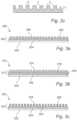
- Fig. 3ais a schematic illustration of a fingerprint sensing device 300 where the cover layer 302 comprises two separate sublayers.
- a first sublayer 304is arranged to cover the sensing elements 204.
- the first sublayer 304may for example be a mold layer used to protect the sensing elements 204 and to form an even surface on which the three-dimensional pattern can be formed.
- the second sublayercomprises a plurality of nanostructures 306 forming the three-dimensional pattern.
- Fig. 3bis a schematic illustration of a fingerprint sensing device 310 where the cover layer 312 comprises two separate sublayers, similar to as shown in Fig. 3a . However, in Fig. 3b , the nanostructures 314 are only formed in a portion of the second sublayer 316.
- Fig. 3cis a schematic illustration of a fingerprint sensing device 320 where the cover layer 322 can be said to comprise three sublayers, 304, 306 and 324, where the top surface of the nanostructures 306 are coated by a reflective material 324 to enhance the reflecting properties of the pattern in order to as efficiently as possible reflect the wavelengths which are not absorbed by the three-dimensional pattern.
- the reflective material 324can for example be a metal.
- Fig. 3dis a schematic illustration of a fingerprint sensing device 330 where the cover layer 332 comprises a first sublayer 304 protecting the sensing elements, a second sublayer 334 comprising a reflective material, and a third sublayer comprising nanostructures 306 forming a three-dimensional pattern.
- the cover layer 332comprises a first sublayer 304 protecting the sensing elements, a second sublayer 334 comprising a reflective material, and a third sublayer comprising nanostructures 306 forming a three-dimensional pattern.
- the reflective materialcannot be electrically conductive as discussed above.
- the patternmay advantageously be configured to also provide hydrophobic or super-hydrophobic surface properties.
- Fig. 3eschematically illustrates a fingerprint sensing device 340 where the cover layer 342 comprises an additional sublayer 344 arranged to cover nanostructures 208 forming the three dimensional pattern.
- the additional layer 344may for example be a mold layer arranged to protect the nanostructures 208.
- Fig. 3fschematically illustrates a fingerprint sensing device 350 where the cover layer 352 comprises a sublayer in the form of a protective plate 354 arranged to cover the three-dimensional pattern and to form an exterior surface 358, i.e. a sensing surface, of the fingerprint sensing device 350.
- the protective platetypically comprises a dielectric material in order to provide a good capacitive coupling between a finger placed on the plate and the sensing elements of the sensing chip.
- the protective platemay advantageously comprise a glass or ceramic material, such as a chemically strengthened glass, ZrO2 or sapphire.
- the aforementioned materialsall provide advantageous properties in that they are hard and thereby resistant to wear and tear, and in that they are dielectric thereby providing a good capacitive coupling between a finger placed on the surface of the protective plate and the sensing element of the sensing device.
- the protective plate 354can be attached to the sensing device using an adhesive 356 arranged between the pattern and the plate 354. The adhesive 356 can thus fill the spaces between the nanostructures so that no air is trapped in the device.
- the material covering the three-dimensional patternis at least partially transparent to visible light so that light can reach the pattern.
- Fig. 4ais a schematic illustration of a fingerprint sensing device 400 according to an embodiment of the invention where different area portions 402a-c of the device 400 have different configurations of the three-dimensional pattern.
- Each area portionmay be referred to as a sub-array or a color pixel 402a-c, which is not to be confused with the sensing element.
- Each color pixelcan have a three-dimensional pattern configured to reduce the amount of reflected light within a specific predetermined sub-range of visible light.
- the pattern and/or the nanostructuresmay be varied in any of the ways discussed above so that each color pixel displays the desired color.
- the color pixels of the three dimensional patterncan have a size which is considerably smaller than the sensing element, thereby providing the possibility to form high resolution images on the surface of the sensing device 400.
- the color pixelmay have a size in the range of 500 nm x 500 nm.
- Fig. 4bschematically illustrates a sensing device where different area portions of the device 408 comprises different types of diffraction gratings as illustrated by the saw-tooth patterns 410a-b and by the elongated ridges 412a-b, where the dimensions of the respective patterns are different to illustrate that each area portion can be tailored to reflect a desired wavelength spectrum. Accordingly, for a diffraction grating different shapes of the nanostructures can be used further to a plasmonic array.
- the illustrated color pixelsalso provides the possibility to combine plasmonic arrays with diffractive gratings in the same plane, where the technique used to achieve the desired color for each particular color pixel can be selected based on which technique provides the better result for the specific color.
- Fig. 5is a flow chart outlining the general steps of a method according to an embodiment of the invention
- Figs. 6a-care schematic illustrations outlining manufacturing steps according to an embodiment of the invention. The method will be described with reference to Figs. 6a-c illustrating a nanoimprint lithography method for forming a three-dimensional pattern in a fingerprint sensing device.
- a sensing chip 602comprising sensing elements (not shown) is provided and the sensing chip is subsequently coated 504 with a cover layer 604 in which the pattern is to be formed.
- the cover layercan for example be a thermoplastic polymer resist.
- An imprint mold 606is provided comprising a reversed/mirrored version of the pattern to be formed in the cover layer 604.
- the imprint mold 606is being pressed onto the cover layer 604 while the cover layer 604 is being heated above the glass transition temperature so that the cover layer 604 becomes soft and deformable. Thereby, the pattern 608 is formed 506 in the cover layer 604.
- the sensing chip 602 and the imprint mold 606is cooled so that the cover layer solidifies, leaving the sensing device with a three-dimensional pattern covering the sensing elements.
- the cover layermay also comprise a UV-curable material in which case the layer is illuminated by UV light to harden after the imprint mold has been pressed into the cover layer.
- Any additional layers described above with reference to Figs. 3a-f ⁇can be formed using conventional and known manufacturing methods.
Landscapes
- Engineering & Computer Science (AREA)
- Human Computer Interaction (AREA)
- Physics & Mathematics (AREA)
- General Physics & Mathematics (AREA)
- Multimedia (AREA)
- Theoretical Computer Science (AREA)
- Measurement Of The Respiration, Hearing Ability, Form, And Blood Characteristics Of Living Organisms (AREA)
- Image Input (AREA)
- Measurement Of Length, Angles, Or The Like Using Electric Or Magnetic Means (AREA)
- Optical Modulation, Optical Deflection, Nonlinear Optics, Optical Demodulation, Optical Logic Elements (AREA)
Description
- The present invention relates to a fingerprint sensing device. In particular, the present invention relates to a surface pattern in a fingerprint sensing device.
- As the development of biometric devices for identity verification, and in particular of fingerprint sensing devices, has lead to devices which are made smaller, cheaper and more energy efficient, the possible applications for such devices are increasing.
- In particular fingerprint sensing has been adopted more and more in, for example, consumer electronic devices, due to small form factor, relatively beneficial cost/performance factor and high user acceptance.
- Capacitive fingerprint sensing devices, built based on CMOS technology for providing the fingerprint sensing elements and auxiliary logic circuitry, are increasingly popular as such sensing devices can be made both small and energy efficient while being able to identify a fingerprint with high accuracy. Thereby, capacitive fingerprint sensors are advantageously used for consumer electronics, such as portable computers, tablet computers and mobile phones, e.g. smartphones.
- The fingerprint sensor may for example be arranged on the front surface of a handheld device, such as a smartphone or tablet computer, in which case the sensor is often arranged having the sensing surface in the same plane as a cover glass for the display of the device. To make the sensor blend in with, or to distinguish the fingerprint senor from the cover glass, it may be desirable to select a particular color or pattern of the fingerprint sensor.
- However, conventional color layers comprising a pigment are rather thick, sometimes more than 40µm for achieving the desired color and glossiness. The thickness influences the sensor performance, since it increases the distance between the finger and the sensing chip. Currently known coating solutions using a pigment are also limited when it comes to the possibility of creating patterns comprising different colors since each color requires a separate processing step, and the resolution of the resulting pattern is limited to about 100µm, depending on the application technology.
- Furthermore, color pigments are molecules which only partially reflect the incident light and the color is defined by light absorption of molecules in the paint. Depending on the desired color, a molecule has to be found that has the required properties and fine tuning of colors is rather difficult. Moreover, as the color is depending on material properties, it may change as the pigment ages.
US2015/0036065 describes a fingerprint sensor incorporated in a display stack in an electronic device. It is further described that a color masking layer may be included over the remote sensing electronics to reduce the visibility of the fingerprint sensor to the user. The color masking layer can be disposed around the peripheral edges of the display layer (above the display layer) so that other components and circuitry can be located in the areas around the display layer and not be visible to the user.- In view of above-mentioned desirable properties of a fingerprint sensing device, and drawbacks of prior art, it is an object of the present invention to provide a fingerprint sensing device and a method for manufacturing a fingerprint sensing device having a colored surface without the use of pigments.
- According to a first aspect of the invention, there is provided a fingerprint sensing device comprising: a sensing chip comprising an array of sensing elements, the sensing elements being configured to be connected to readout circuitry for detecting a capacitive coupling between each of the sensing elements and a finger placed on a sensing surface of the sensing device; a cover layer arranged vertically above the sensing elements to cover at least a portions of the sensing elements, wherein an outer surface of the cover layer form the sensing surface of the sensing device; wherein the cover layer comprises a three-dimensional (3D) pattern configured to reduce the amount of reflected light within a predetermined sub-range of the visible range, the three-dimensional pattern being a plasmonic array comprising a plurality of electrically conductive nanostructures, wherein said nanostructures are galvanically isolated from each other.
- That the cover layer is arranged vertically above the sensing elements does not exclude that there may be additional layers arranged between the cover layer and the sensing elements. That the cover layer comprises a three dimensional pattern means that the pattern comprises individual features which have an extension in three dimensions.
- The present invention is based on the realization that a fingerprint sensor can be made which can be tailored to have a desired visual appearance of the surface by using a cover layer comprising a three-dimensional pattern configured to reduce the amount of reflected light within a predetermined sub-range of the visible range, thereby achieving a particular color of the sensing device.
- Since fingerprint sensors in general comprise some type of cover layer to physically protect the sensing elements. By achieving the desired effects with respect to visual appearance of the fingerprint sensor using a three dimensional pattern comprised in the cover layer, no additional materials are required which is the case e.g. when using pigments. Furthermore, different colors can be achieved by tailoring the three-dimensional pattern with respect to size, shape of pattern and material composition. Furthermore, a higher resolution can be achieved compared to what is known for currently used methods using pigments.
- The plasmonic array further comprises an array of plasmonic nanostructures where the nanostructures are galvanically isolated from each other. In the present context, nanostructures generally refers to structures having at least one dimension, and typically all three dimensions, in the nanometer range. The nanometer range is considered to reach up to and including 1000 nm.
- According to one embodiment of the invention, a size, shape and distribution of the nanostructures is selected to form a plasmonic array configured to reduce the amount of reflected light within a predetermined sub-range of the visible range. Plasmonic nanostructures can be pillars, cubes, holes, discs, or particles with any shape. The incident light excites localized surface electron plasma oscillations in the nano-scale structures. The structures have a size basically in the range of the wavelength of visible light. By exciting the localized surface plasmons the incident light is partly absorbed. Since white light consists of a spectrum of different wavelengths the light changes the color if some of the wavelengths are absorbed. Which part of the light is absorbed depends on the size and periodicity of the nanostructures. This enables the possibility to change the color appearance of a sample with nanostructures by changing the size and periodicity of the pattern. Since the plasmonic action depends in individual electrically conductive nanostructures, the nanostructures are galvanically isolated from each other so as to not form a conductive path between adjacent nanostructures.
- According to one embodiment of the invention, the cover layer comprises a plurality of sub-layers. Accordingly, the cover layer must not be a homogeneous layer and the cover layer may thus comprise two or more sublayers to form a stack of sublayers. Furthermore, one or more additional layers or structures may be arranged on top of or below the cover layer. In applications where sublayers or structures are arranged on top of the three-dimensional pattern, such layers must be at least partially transparent for the three-dimensional pattern to have any effect with respect to the visual appearance of the sensor.
- In one embodiment of the invention, the three-dimensional pattern is arranged in a first sub-layer which is covered by a second sub-layer. The three-dimensional pattern may require a protection layer to provide mechanical protection for the small structures constituting the array. The second sub-layer may preferably be transparent to allow light to pass through the second sublayer without absorption. Such a transparent layer may for example be a transparent material coated onto the three-dimensional pattern, or it may be a glass cover plate.
- According to one embodiment of the invention, the three-dimensional pattern is arranged at the sensing surface, and the pattern may advantageously be configured to provide hydrophobic surface properties. In addition to the wavelength reflection properties of the pattern, they may further be configured to provide a surface which repels water, which improves the performance of the fingerprint sensing device by reducing the amount of water adhering to the sensing surface. The structures may either cause a roughness that increases the actual contact line between droplet and substrate surface (Wenzel model) or cause air pockets between the surface and the water droplets that prevents the droplet from touching the surface (Cassie-Baxter model). In both cases the hydrophobicity of a material is increased. To enhance the hydrophobic effect, the structures can be as large as 10 µm.
- According to one embodiment of the invention, the three-dimensional pattern is configured to reduce the amount of reflected light within different predetermined sub-ranges of the visible range for different area portions of the sensing device such that an image is formed on the sensing surface. By changing the size and periodicity of the structure locally, pixels with different individually designed colors can be designed allowing colored patterns or even full color photo-like images with high resolution. Since the structures allow a very high resolution and are difficult to copy, this technology can also be used to create watermarks or other anti-counterfeiting features.
- In one embodiment of the invention, the three-dimensional pattern is configured such that the predetermined sub-range is different for different viewing angles. Depending on the configuration of the three-dimensional pattern, also angle dependencies of the color can be achieved. Thereby holographic effects can be achieved which have a very small feature size and which are difficult to replicate, thereby providing an efficient method of ensuring the authenticity of the fingerprint sensing device.
- According to one embodiment of the invention, at least a portion of the cover layer is coated by an optically reflecting material. For example, at least protruding portions of the three-dimensional pattern may be coated by an optically reflecting material. To achieve brighter or more reflective colors a metal can be applied on top of the structure or the structure itself can consist of metal. Such a reflecting metal layer cannot be a conductive sheet, which means it has to consist of isolated metal islands. A reflective layer may also be arranged as a background layer such that light which is not reflected by the three-dimensional pattern can be reflected by the reflecting layer.
- According to a second aspect of the invention, there is provided a method for manufacturing a fingerprint sensing device, the method comprising: providing a sensing chip comprising an array of sensing elements, the sensing elements being configured to be connected to readout circuitry for detecting a capacitive coupling between each of the sensing elements and a finger placed on a sensing surface of the sensing device; forming a cover layer arranged vertically above the sensing elements to cover at least a portions of the sensing elements, wherein an outer surface of the cover layer form the sensing surface of the sensing device; and in the cover layer, forming a three-dimensional pattern configured to reduce the amount of reflected light within a predetermined sub-range of the visible range, the three-dimensional pattern being a plasmonic array comprising a plurality of electrically conductive nanostructures, wherein said nanostructures are galvanically isolated from each other.
- In one embodiment of the invention, the step of forming a three-dimensional pattern advantageously comprises nanoimprint lithography or photolithography. Both photolithography and nanoimprint lithography (NIL) are methods which may be used for large scale production. NIL can be used at a low cost and with a high throughput. NIL is based on replicating a master that has the inverse of the desired nano- or micro-patterns. The master is pressed on a substrate to deform a thermoplastic or UV-curable layer. For large scale applications roll to roll NIL or mold inserts are available. Furthermore, pattern created by NIL can more easily have a high resolution compared to patterns formed by photolithography.
- According to one embodiment of the invention, the method further comprises depositing a reflective coating on protruding portions of the three-dimensional pattern.
- Additional advantages, effects and features of the second aspect of the invention are largely analogous to those described above in connection with the first aspect of the invention.
- Further features of, and advantages with, the present invention will become apparent when studying the appended claims and the following description. The skilled person realize that different features of the present invention may be combined to create embodiments other than those described in the following, without departing from the scope of the appended claims.
- These and other aspects of the present invention will now be described in more detail, with reference to the appended drawings showing an example embodiment of the invention, wherein:
Fig. 1 schematically illustrates a handheld electronic device comprising a fingerprint sensing device according to an embodiment of the invention;Figs. 2a-c schematically illustrate a fingerprint sensing device according to an embodiment of the invention;Figs. 3a-f schematically illustrate fingerprint sensing devices according to embodiments of the invention;Figs. 4a-b schematically illustrate fingerprint sensing devices according to an embodiment of the invention;Fig. 5 is a flow chart outlining the general steps of a method according to an embodiment of the invention; andFigs. 6a-c schematically illustrates a method of manufacturing a fingerprint sensing device according to an embodiment of the invention.- In the present detailed description, various embodiments of a fingerprint sensing device according to the present invention are mainly discussed with reference to a capacitive fingerprint sensing device. A method for manufacturing a fingerprint sensing device is also discussed.
Fig. 1 is a schematic illustration of ahandheld device 100 comprising afingerprint sensing device 102 comprising atouchscreen display 104. Afingerprint sensing device 102 can be used in for example a mobile phone, a tablet computer, a portable computer or any other electronic device requiring a way to identify and/or authenticate a user.Figs. 2a-b are schematic illustrations of afingerprint sensing device 200 according to an embodiment of the invention. It should be noted that the drawings are not made to scale and that they serve to illustrate general concepts of various embodiments of the invention. The exterior surface of thesensing device 200 is referred to as the sensing surface, since that is the surface where a finger will be placed for capturing a fingerprint image. The fingerprint sensing device is based on asensing chip 202 comprising an array of sensingelements 204. Thesensing elements 204 are here shown as square elements arranged in a square array. Typically, the sensing elements have a size of about 50x50 µm and a distance between adjacent elements is about 5 µm. Thesensing elements 204 are electrically conductive, typically metallic, and can as a general approximation be considered to act as one plate in a parallel plate capacitor, where a finger placed on a sensing surface of thefingerprint sensing device 200 represents the other plate. Eachsensing element 204 is connected to readout circuitry (not shown) for detecting a capacitive coupling between each of saidsensing elements 204 and a finger placed on the sensing surface 201 in order to capture a fingerprint image.- The sensing device further comprises a
cover layer 206 arranged on top of thesensing elements 204, and thecover layer 206 is typically arranged to cover the entire area of thesensing chip 202. Furthermore, the cover layer comprises a three-dimensional pattern configured to reduce the amount of reflected light within a predetermined sub-range of the visible range, such that the visual appearance of thesensing device 200 can be tailored to exhibit a selected color. The three-dimensional pattern comprises a plurality ofnanostructures 208 arranged in an array. The three-dimensional pattern is a plasmonic array. The nanostructures are electrically conductive, typically metallic. - The nanostructures are galvanically isolated from each other, in order to not disturb the capacitive sensing mechanism of the fingerprint sensing device. However, parts of the overall ensemble of nanostructures may be electrically connected, as long as the resulting connected portions do not disturb the operation of the sensing elements. Typically, such connected portions cannot be larger than the sensing elements or be arranged to overlap multiple sensing elements. For example, when the nanostructures are provided in the form of an array of holes in a conductive layer, the conductive layer is interrupted on a larger scale, for example in alignment with the sensing elements.
Fig. 2c outline some of the parameters determining the properties of the three-dimensional pattern, and of thenanostructures 208, determining the reflection properties of the pattern, where d represents the width or diameter of ananostructure 208, s is the distance (spacing) betweenadjacent nanostructures 208, p is the pitch, and h is the height of thenanostructure 208. Even though the pattern is here illustrated as a regular square array comprising square nanostructures, different configurations of the pattern are possible and the nanostructure may have different shapes, such as cylindrical, pyramid-shaped, conical, or a truncated cone or pyramid. The nanostructures may also be pillars, cubes, holes, discs, or particles with an arbitrary shape. For a three-dimensional pattern in the form of a reflecting diffraction grating, the nanostructures may be elongated as will be illustrated below.- As an example the
nanostructures 208 for a plasmonic array may have a height of about 150 nm, a diameter of about 200 nm, a spacing of about 300 nm with a periodicity of about 500 nm. It should be noted that various embodiments of the present invention are by no means limited to structures according to the above, and that the given example merely describe the order of magnitude of the size of the nanostructures. Specific example on how to form nanostructure arrays for reflecting different wavelengths can for example be found inGu et al, Nanoscale, 2015, 7, 6409. - For a diffraction grating, the sizes are about the same as above, but other shapes are possible.
Fig. 3a is a schematic illustration of afingerprint sensing device 300 where the cover layer 302 comprises two separate sublayers. Afirst sublayer 304 is arranged to cover thesensing elements 204. Thefirst sublayer 304 may for example be a mold layer used to protect thesensing elements 204 and to form an even surface on which the three-dimensional pattern can be formed. The second sublayer comprises a plurality ofnanostructures 306 forming the three-dimensional pattern.Fig. 3b is a schematic illustration of afingerprint sensing device 310 where the cover layer 312 comprises two separate sublayers, similar to as shown inFig. 3a . However, inFig. 3b , thenanostructures 314 are only formed in a portion of thesecond sublayer 316.Fig. 3c is a schematic illustration of afingerprint sensing device 320 where thecover layer 322 can be said to comprise three sublayers, 304, 306 and 324, where the top surface of thenanostructures 306 are coated by areflective material 324 to enhance the reflecting properties of the pattern in order to as efficiently as possible reflect the wavelengths which are not absorbed by the three-dimensional pattern. Thereflective material 324 can for example be a metal.Fig. 3d is a schematic illustration of afingerprint sensing device 330 where thecover layer 332 comprises afirst sublayer 304 protecting the sensing elements, asecond sublayer 334 comprising a reflective material, and a thirdsublayer comprising nanostructures 306 forming a three-dimensional pattern. In the case of areflective material layer 334 covering substantially the entire surface of thesensing chip 202, the reflective material cannot be electrically conductive as discussed above.- In the embodiments described above where the three dimensional pattern forms the outer surface of the fingerprint sensing device, the pattern may advantageously be configured to also provide hydrophobic or super-hydrophobic surface properties.
Fig. 3e schematically illustrates afingerprint sensing device 340 where the cover layer 342 comprises anadditional sublayer 344 arranged to covernanostructures 208 forming the three dimensional pattern. Theadditional layer 344 may for example be a mold layer arranged to protect thenanostructures 208.Fig. 3f schematically illustrates afingerprint sensing device 350 where the cover layer 352 comprises a sublayer in the form of aprotective plate 354 arranged to cover the three-dimensional pattern and to form anexterior surface 358, i.e. a sensing surface, of thefingerprint sensing device 350. The protective plate typically comprises a dielectric material in order to provide a good capacitive coupling between a finger placed on the plate and the sensing elements of the sensing chip. In particular, the protective plate may advantageously comprise a glass or ceramic material, such as a chemically strengthened glass, ZrO2 or sapphire. The aforementioned materials all provide advantageous properties in that they are hard and thereby resistant to wear and tear, and in that they are dielectric thereby providing a good capacitive coupling between a finger placed on the surface of the protective plate and the sensing element of the sensing device. Theprotective plate 354 can be attached to the sensing device using an adhesive 356 arranged between the pattern and theplate 354. The adhesive 356 can thus fill the spaces between the nanostructures so that no air is trapped in the device.- In the embodiments described with reference to
figs. 3e-f , the material covering the three-dimensional pattern is at least partially transparent to visible light so that light can reach the pattern. - Based on the embodiments described in
Fig. 3a-f , the skilled person readily realizes that the embodiments may be combined in many different ways leading to configurations of sensing devices not explicitly described herein. It should thus be understood that the present inventive concept is equally applicable to a large number of possible configurations of a fingerprint sensing device. Fig. 4a is a schematic illustration of afingerprint sensing device 400 according to an embodiment of the invention wheredifferent area portions 402a-c of thedevice 400 have different configurations of the three-dimensional pattern. Each area portion may be referred to as a sub-array or acolor pixel 402a-c, which is not to be confused with the sensing element. Each color pixel can have a three-dimensional pattern configured to reduce the amount of reflected light within a specific predetermined sub-range of visible light. The pattern and/or the nanostructures may be varied in any of the ways discussed above so that each color pixel displays the desired color. Furthermore, the color pixels of the three dimensional pattern can have a size which is considerably smaller than the sensing element, thereby providing the possibility to form high resolution images on the surface of thesensing device 400. For example, the color pixel may have a size in the range of 500 nm x 500 nm.Fig. 4b schematically illustrates a sensing device where different area portions of thedevice 408 comprises different types of diffraction gratings as illustrated by the saw-tooth patterns 410a-b and by the elongatedridges 412a-b, where the dimensions of the respective patterns are different to illustrate that each area portion can be tailored to reflect a desired wavelength spectrum. Accordingly, for a diffraction grating different shapes of the nanostructures can be used further to a plasmonic array.- The illustrated color pixels also provides the possibility to combine plasmonic arrays with diffractive gratings in the same plane, where the technique used to achieve the desired color for each particular color pixel can be selected based on which technique provides the better result for the specific color. As an alternative configuration, it would also be possible to provide to stacked layers where a first layer comprises a plasmonic array and where a second layer comprises a diffractive grating.
- A detailed example on how to form plasmonic arrays having different wavelength reflecting properties can for example be found in"Reflective plasmonic color filters based on lithographically patterned silver nanorod arrays", Si et. al, Nanoscale, 2013, 5, 6243.
Fig. 5 is a flow chart outlining the general steps of a method according to an embodiment of the invention, andFigs. 6a-c are schematic illustrations outlining manufacturing steps according to an embodiment of the invention. The method will be described with reference toFigs. 6a-c illustrating a nanoimprint lithography method for forming a three-dimensional pattern in a fingerprint sensing device.- First 502, a sensing chip 602 comprising sensing elements (not shown) is provided and the sensing chip is subsequently coated 504 with a cover layer 604 in which the pattern is to be formed. The cover layer can for example be a thermoplastic polymer resist. An
imprint mold 606 is provided comprising a reversed/mirrored version of the pattern to be formed in the cover layer 604. - Next, the
imprint mold 606 is being pressed onto the cover layer 604 while the cover layer 604 is being heated above the glass transition temperature so that the cover layer 604 becomes soft and deformable. Thereby, the pattern 608 is formed 506 in the cover layer 604. - Finally, the sensing chip 602 and the
imprint mold 606 is cooled so that the cover layer solidifies, leaving the sensing device with a three-dimensional pattern covering the sensing elements. - The cover layer may also comprise a UV-curable material in which case the layer is illuminated by UV light to harden after the imprint mold has been pressed into the cover layer.
- Any additional layers described above with reference to
Figs. 3a-f \ can be formed using conventional and known manufacturing methods. - Additionally, variations to the disclosed embodiments, without departing from the scope of the appended claims, can be understood and effected by the skilled person in practicing the claimed invention, from a study of the drawings, the disclosure, and the appended claims. In the claims, the word "comprising" does not exclude other elements or steps, and the indefinite article "a" or "an" does not exclude a plurality. The mere fact that certain measures are recited in mutually different dependent claims does not indicate that a combination of these measured cannot be used to advantage.
Claims (13)
- A fingerprint sensing device (200) comprising:a sensing chip (202) comprising an array of sensing elements (204), said sensing elements being configured to be connected to readout circuitry for detecting a capacitive coupling between each of said sensing elements and a finger placed on a sensing surface of said sensing device;a cover layer (206) arranged vertically above said sensing elements to cover at least a portion of said sensing elements, wherein an outer surface of said cover layer forms said sensing surface of said sensing device;characterized in that said cover layer comprises a three-dimensional pattern (208, 410a-b, 412a-b) configured to reduce the amount of reflected light within a predetermined sub-range of the visible range, the three-dimensional pattern being a plasmonic array comprising a plurality of electrically conductive nanostructures (208), wherein said nanostructures are galvanically isolated from each other.
- The sensing device according to claim 1, wherein a size, shape and distribution of said nanostructures is selected to form a plasmonic array configured to reduce the amount of reflected light within a predetermined sub-range of the visible range.
- The sensing device according to any one of the preceding claims, wherein said cover layer comprises a plurality of sub-layers.
- The sensing device according to claim 1, wherein said three-dimensional pattern is arranged in a first sub-layer which is covered by a second sub-layer.
- The sensing device according to any one of the preceding claims, wherein said cover layer comprises a first area portion where said three-dimensional pattern is configured to reduce the amount of reflected light within a first predetermined sub-range, and a second area portion where said three-dimensional pattern is configured to reduce the amount of reflected light within a second predetermined sub-range, wherein said first sub-range is different from said second sub-range.
- The sensing device according to any one of the preceding claims, wherein said three-dimensional pattern is arranged at said sensing surface, and wherein said pattern is configured to provide hydrophobic surface properties.
- The sensing device according to any one of the preceding claims, wherein said three-dimensional pattern is configured to reduce the amount of reflected light within different predetermined sub-ranges of the visible range for different area portions of the sensing device such that an image is formed on said sensing surface.
- The sensing device according to any one of the preceding claims, wherein said three-dimensional pattern is configured such that the predetermined sub-range is different for different viewing angles.
- The sensing device according to any one of the preceding claims, wherein at least a portion of said cover layer is coated by an optically reflecting material.
- The sensing device according to any one of the preceding claims, wherein at least protruding portions of said three-dimensional pattern are coated by an optically reflecting material.
- A method for manufacturing a fingerprint sensing device (200), said method comprising:providing (502) a sensing chip (202) comprising an array of sensing elements (204), said sensing elements being configured to be connected to readout circuitry for detecting a capacitive coupling between each of said sensing elements and a finger placed on a sensing surface of said sensing device;forming (504) a cover layer (206) arranged vertically above said sensing elements to cover at least a portion of said sensing elements, wherein an outer surface of said cover layer forms said sensing surface of said sensing device; andthe method beingcharacterized by, in said cover layer, forming (506) a three-dimensional pattern (208, 410a-b, 412a-b) configured to reduce the amount of reflected light within a predetermined sub-range of the visible range, the three-dimensional pattern being a plasmonic array comprising a plurality of electrically conductive nanostructures (208), wherein said nanostructures are galvanically isolated from each other.
- The method according to claim 11, wherein said step of forming a three-dimensional pattern comprises nanoimprint lithography or photolithography.
- The method according to claim 11 or 12, further comprising depositing a reflective coating on protruding portions of said three-dimensional pattern.
Applications Claiming Priority (2)
| Application Number | Priority Date | Filing Date | Title |
|---|---|---|---|
| SE1550957 | 2015-07-03 | ||
| PCT/SE2016/050637WO2017007400A1 (en) | 2015-07-03 | 2016-06-27 | Fingerprint sensing device comprising three-dimensional pattern |
Publications (3)
| Publication Number | Publication Date |
|---|---|
| EP3317701A1 EP3317701A1 (en) | 2018-05-09 |
| EP3317701A4 EP3317701A4 (en) | 2018-12-26 |
| EP3317701B1true EP3317701B1 (en) | 2023-07-19 |
Family
ID=57685363
Family Applications (1)
| Application Number | Title | Priority Date | Filing Date |
|---|---|---|---|
| EP16821733.9AActiveEP3317701B1 (en) | 2015-07-03 | 2016-06-27 | Fingerprint sensing device comprising three-dimensional pattern |
Country Status (6)
| Country | Link |
|---|---|
| US (1) | US9524416B1 (en) |
| EP (1) | EP3317701B1 (en) |
| JP (1) | JP6759253B2 (en) |
| KR (1) | KR20180025862A (en) |
| CN (1) | CN106662682B (en) |
| WO (1) | WO2017007400A1 (en) |
Families Citing this family (15)
| Publication number | Priority date | Publication date | Assignee | Title |
|---|---|---|---|---|
| US8485442B2 (en) | 2009-07-02 | 2013-07-16 | Biometric Payment Solutions | Electronic transaction verification system with biometric authentication |
| ES2979111T3 (en) | 2015-07-06 | 2024-09-24 | Turning Point Therapeutics Inc | Diaryl macrocycle polymorph |
| KR20180098124A (en) | 2017-01-19 | 2018-09-03 | 선전 구딕스 테크놀로지 컴퍼니, 리미티드 | Fingerprint recognition device and method of making the same |
| CN107808853B (en)* | 2017-11-14 | 2019-09-24 | 苏州科阳光电科技有限公司 | A kind of fingerprint chip-packaging structure and production method, terminal device |
| KR102808360B1 (en)* | 2019-01-04 | 2025-05-19 | 삼성디스플레이 주식회사 | Fingerprint sensor and display device including the same |
| CN111208651A (en)* | 2019-07-22 | 2020-05-29 | 神亚科技股份有限公司 | imaging system |
| CN111145071B (en)* | 2019-12-23 | 2021-10-22 | 武汉大学 | A three-channel metasurface multiplexing method for superimposing watermarks in continuous grayscale images |
| TWI785408B (en)* | 2020-03-02 | 2022-12-01 | 神盾股份有限公司 | Integrated spectrum sensing device for real-finger judgement and sensing method |
| WO2021197677A1 (en)* | 2020-04-02 | 2021-10-07 | Nil Technology Aps | Metasurface coatings |
| CN111461040B (en)* | 2020-04-07 | 2024-11-19 | 武汉华星光电技术有限公司 | Electronic device and optical fingerprint recognition module thereof |
| GB2621408A (en)* | 2022-08-12 | 2024-02-14 | Touch Biometrix Ltd | Sensors and methods |
| EP4568569A1 (en)* | 2022-08-12 | 2025-06-18 | Touch Biometrix Limited | Sensors and methods |
| GB2621409A (en)* | 2022-08-12 | 2024-02-14 | Touch Biometrix Ltd | Sensors and methods |
| WO2024092243A1 (en)* | 2022-10-28 | 2024-05-02 | Arizona Board Of Regents On Behalf Of The University Of Arizona | Glass mirror substrates for non-specular reflection |
| US20240322056A1 (en)* | 2023-03-21 | 2024-09-26 | Visera Technologies Company Ltd. | Optical device |
Citations (5)
| Publication number | Priority date | Publication date | Assignee | Title |
|---|---|---|---|---|
| US3968476A (en)* | 1974-07-17 | 1976-07-06 | Sperry Rand Corporation | Spurious signal removal in optical processor fingerprint identification apparatus |
| CA2529147A1 (en)* | 2003-06-21 | 2005-01-06 | Aprilis, Inc. | Acquisition of high resolution biometric images |
| KR20080050460A (en)* | 2005-09-01 | 2008-06-05 | 루미다임 인크. | Biometric sensors |
| US20120249797A1 (en)* | 2010-02-28 | 2012-10-04 | Osterhout Group, Inc. | Head-worn adaptive display |
| US8284019B2 (en)* | 2007-05-08 | 2012-10-09 | Davar Pishva | Spectroscopic method and system for multi-factor biometric authentication |
Family Cites Families (25)
| Publication number | Priority date | Publication date | Assignee | Title |
|---|---|---|---|---|
| US4353056A (en)* | 1980-06-05 | 1982-10-05 | Siemens Corporation | Capacitive fingerprint sensor |
| US6411726B1 (en)* | 1998-10-08 | 2002-06-25 | Durel Corporation | Fingerprint detector using an EL lamp |
| JP2005055327A (en)* | 2003-08-05 | 2005-03-03 | Sony Corp | Fingerprint collation device |
| JP4604087B2 (en)* | 2004-06-18 | 2010-12-22 | フィンガープリント カーズ アーベー | Fingerprint sensor element |
| TW200737486A (en)* | 2006-03-24 | 2007-10-01 | Lightuning Tech Inc | Semiconductor integrated circuit chip with nano-structure-surface resin passivation and method of fabricating the same |
| JP4621270B2 (en)* | 2007-07-13 | 2011-01-26 | キヤノン株式会社 | Optical filter |
| JP5300495B2 (en)* | 2009-01-06 | 2013-09-25 | 株式会社東芝 | Metal thin film composite having selective light transmission characteristics and method for producing the same |
| KR101649700B1 (en)* | 2009-12-28 | 2016-08-19 | 엘지디스플레이 주식회사 | Method of fabricating master mold and method of fabricating surface plasmon color filter using the same |
| EP2558978B1 (en)* | 2010-04-15 | 2016-06-29 | Apple Inc. | Finger sensor including capacitive lens and associated methods |
| WO2011139785A2 (en)* | 2010-04-27 | 2011-11-10 | The Regents Of The University Of Michigan | Display device having plasmonic color filters and photovoltaic capabilities |
| US20120090757A1 (en)* | 2010-10-18 | 2012-04-19 | Qualcomm Mems Technologies, Inc. | Fabrication of touch, handwriting and fingerprint sensor |
| JP5080660B2 (en)* | 2011-01-05 | 2012-11-21 | エイエスディ株式会社 | Fingerprint reader |
| WO2012169656A1 (en)* | 2011-06-09 | 2012-12-13 | Sharp Kabushiki Kaisha | Touch-enabled plasmonic reflective display and method for changing the reflected colors |
| DE102012108170B4 (en)* | 2012-09-03 | 2015-01-22 | Bundesdruckerei Gmbh | Security element and method for producing a security element |
| KR101974581B1 (en)* | 2012-09-24 | 2019-05-02 | 삼성전자주식회사 | 3-dimensional nanoplasmonic structure and method of manufacturing the same |
| SG2013073085A (en)* | 2012-09-28 | 2014-04-28 | Agency Science Tech & Res | Method of writing to an optical data storage medium, method of reading from an optical data storage medium, and optical data storage medium |
| US9547107B2 (en)* | 2013-03-15 | 2017-01-17 | The Regents Of The University Of Michigan | Dye and pigment-free structural colors and angle-insensitive spectrum filters |
| US9984270B2 (en) | 2013-08-05 | 2018-05-29 | Apple Inc. | Fingerprint sensor in an electronic device |
| US9311545B2 (en)* | 2013-09-18 | 2016-04-12 | Blackberry Limited | Multicolor biometric scanning user interface |
| US9418273B2 (en)* | 2013-09-18 | 2016-08-16 | Blackberry Limited | Structure for multicolor biometric scanning user interface |
| US20150124306A1 (en)* | 2013-11-06 | 2015-05-07 | Lehigh University | Ultrathin nanostructured metals for highly transmissive plasmonic subtractive color filters |
| KR101700998B1 (en)* | 2014-01-02 | 2017-01-31 | 삼성전기주식회사 | Sensor for detecting fingerprint and electronic device including the same |
| CN103955679B (en)* | 2014-05-19 | 2017-12-15 | 上海天马微电子有限公司 | Color film substrate, array substrate and display device |
| US9489604B2 (en)* | 2014-06-03 | 2016-11-08 | IE-9 Technology Corp. | Optically variable data storage device |
| US20160086044A1 (en)* | 2014-09-24 | 2016-03-24 | Au Optronics Corporation | Optical Device and Optical Scanning Method Thereof |
- 2016
- 2016-02-17USUS15/045,379patent/US9524416B1/enactiveActive
- 2016-06-27CNCN201680002230.9Apatent/CN106662682B/enactiveActive
- 2016-06-27KRKR1020177036257Apatent/KR20180025862A/ennot_activeCeased
- 2016-06-27JPJP2017565962Apatent/JP6759253B2/enactiveActive
- 2016-06-27WOPCT/SE2016/050637patent/WO2017007400A1/ennot_activeCeased
- 2016-06-27EPEP16821733.9Apatent/EP3317701B1/enactiveActive
Patent Citations (5)
| Publication number | Priority date | Publication date | Assignee | Title |
|---|---|---|---|---|
| US3968476A (en)* | 1974-07-17 | 1976-07-06 | Sperry Rand Corporation | Spurious signal removal in optical processor fingerprint identification apparatus |
| CA2529147A1 (en)* | 2003-06-21 | 2005-01-06 | Aprilis, Inc. | Acquisition of high resolution biometric images |
| KR20080050460A (en)* | 2005-09-01 | 2008-06-05 | 루미다임 인크. | Biometric sensors |
| US8284019B2 (en)* | 2007-05-08 | 2012-10-09 | Davar Pishva | Spectroscopic method and system for multi-factor biometric authentication |
| US20120249797A1 (en)* | 2010-02-28 | 2012-10-04 | Osterhout Group, Inc. | Head-worn adaptive display |
Also Published As
| Publication number | Publication date |
|---|---|
| EP3317701A1 (en) | 2018-05-09 |
| US20170004342A1 (en) | 2017-01-05 |
| JP6759253B2 (en) | 2020-09-23 |
| EP3317701A4 (en) | 2018-12-26 |
| US9524416B1 (en) | 2016-12-20 |
| WO2017007400A1 (en) | 2017-01-12 |
| CN106662682B (en) | 2018-01-09 |
| KR20180025862A (en) | 2018-03-09 |
| JP2018533030A (en) | 2018-11-08 |
| CN106662682A (en) | 2017-05-10 |
Similar Documents
| Publication | Publication Date | Title |
|---|---|---|
| EP3317701B1 (en) | Fingerprint sensing device comprising three-dimensional pattern | |
| AU2022263490B2 (en) | An improved polymeric sheet material for use in making polymeric security documents such as banknotes | |
| CN108027521B (en) | Optical product, master for making optical product, and method for making master and optical product | |
| TWI765870B (en) | Thin film and method for producing the same, electrically acting member including the thin film, and method for producing the same | |
| JP5186378B2 (en) | Multilayer body and method for producing the same | |
| US12253691B2 (en) | Optical products, masters for fabricating optical products, and methods for manufacturing masters and optical products | |
| CN106199799B (en) | Colour anti-counterfeit structure body and coloring anti-counterfeiting medium | |
| US10409331B2 (en) | Cover glass for electronic device | |
| US7864424B2 (en) | Zero order pigments (ZOP) | |
| CN108454264B (en) | Optical anti-counterfeiting element and optical anti-counterfeiting product using same | |
| KR102414589B1 (en) | Multi-layer body and method for producing same | |
| CN106574997A (en) | Counterfeit preventing structure and counterfeit preventing article | |
| CN102236462A (en) | Transparent conducting element, information input device and display device | |
| CN108454266B (en) | Optical anti-counterfeiting element and optical anti-counterfeiting product | |
| CA3195166A1 (en) | Optical products, masters for fabricating optical products, and methods for manufacturing masters and optical products | |
| CN105378514A (en) | Solar light management | |
| KR101534327B1 (en) | Dual color-shifting security element and security product comprising the same | |
| JP7691538B2 (en) | Complete Micro Optical Security Document | |
| JP6186837B2 (en) | Display body, article with display body, and method for determining authenticity thereof | |
| Ji et al. | Lenticular‐Lens‐Based Colored Antiglare Dashboard Surfaces | |
| US20240337854A1 (en) | Optical film for controlling optical path, and manufacturing method therefor | |
| CN116118382A (en) | Security element and security product | |
| JP6277712B2 (en) | Indicator | |
| WO2017164403A1 (en) | Electromagnetic-wave-responsive laminate |
Legal Events
| Date | Code | Title | Description |
|---|---|---|---|
| STAA | Information on the status of an ep patent application or granted ep patent | Free format text:STATUS: THE INTERNATIONAL PUBLICATION HAS BEEN MADE | |
| PUAI | Public reference made under article 153(3) epc to a published international application that has entered the european phase | Free format text:ORIGINAL CODE: 0009012 | |
| STAA | Information on the status of an ep patent application or granted ep patent | Free format text:STATUS: REQUEST FOR EXAMINATION WAS MADE | |
| 17P | Request for examination filed | Effective date:20171204 | |
| AK | Designated contracting states | Kind code of ref document:A1 Designated state(s):AL AT BE BG CH CY CZ DE DK EE ES FI FR GB GR HR HU IE IS IT LI LT LU LV MC MK MT NL NO PL PT RO RS SE SI SK SM TR | |
| AX | Request for extension of the european patent | Extension state:BA ME | |
| DAV | Request for validation of the european patent (deleted) | ||
| DAX | Request for extension of the european patent (deleted) | ||
| A4 | Supplementary search report drawn up and despatched | Effective date:20181126 | |
| RIC1 | Information provided on ipc code assigned before grant | Ipc:B82Y 20/00 20110101ALI20181120BHEP Ipc:G06K 9/00 20060101ALI20181120BHEP Ipc:G01N 21/552 20140101ALI20181120BHEP Ipc:A61B 5/117 20160101ALI20181120BHEP Ipc:G02B 5/00 20060101AFI20181120BHEP Ipc:G02B 5/18 20060101ALI20181120BHEP | |
| STAA | Information on the status of an ep patent application or granted ep patent | Free format text:STATUS: EXAMINATION IS IN PROGRESS | |
| 17Q | First examination report despatched | Effective date:20200423 | |
| RAP1 | Party data changed (applicant data changed or rights of an application transferred) | Owner name:FINGERPRINT CARDS ANACATUM IP AB | |
| REG | Reference to a national code | Ref country code:DE Ref legal event code:R079 Free format text:PREVIOUS MAIN CLASS: G02B0005000000 Ipc:G06V0040130000 Ref country code:DE Ref legal event code:R079 Ref document number:602016081201 Country of ref document:DE Free format text:PREVIOUS MAIN CLASS: G02B0005000000 Ipc:G06V0040130000 | |
| GRAP | Despatch of communication of intention to grant a patent | Free format text:ORIGINAL CODE: EPIDOSNIGR1 | |
| STAA | Information on the status of an ep patent application or granted ep patent | Free format text:STATUS: GRANT OF PATENT IS INTENDED | |
| RIC1 | Information provided on ipc code assigned before grant | Ipc:G06V 40/13 20220101AFI20230206BHEP | |
| INTG | Intention to grant announced | Effective date:20230220 | |
| GRAS | Grant fee paid | Free format text:ORIGINAL CODE: EPIDOSNIGR3 | |
| GRAA | (expected) grant | Free format text:ORIGINAL CODE: 0009210 | |
| STAA | Information on the status of an ep patent application or granted ep patent | Free format text:STATUS: THE PATENT HAS BEEN GRANTED | |
| AK | Designated contracting states | Kind code of ref document:B1 Designated state(s):AL AT BE BG CH CY CZ DE DK EE ES FI FR GB GR HR HU IE IS IT LI LT LU LV MC MK MT NL NO PL PT RO RS SE SI SK SM TR | |
| REG | Reference to a national code | Ref country code:GB Ref legal event code:FG4D | |
| REG | Reference to a national code | Ref country code:CH Ref legal event code:EP | |
| REG | Reference to a national code | Ref country code:DE Ref legal event code:R096 Ref document number:602016081201 Country of ref document:DE | |
| REG | Reference to a national code | Ref country code:IE Ref legal event code:FG4D | |
| REG | Reference to a national code | Ref country code:LT Ref legal event code:MG9D | |
| REG | Reference to a national code | Ref country code:NL Ref legal event code:MP Effective date:20230719 | |
| REG | Reference to a national code | Ref country code:AT Ref legal event code:MK05 Ref document number:1590264 Country of ref document:AT Kind code of ref document:T Effective date:20230719 | |
| PG25 | Lapsed in a contracting state [announced via postgrant information from national office to epo] | Ref country code:NL Free format text:LAPSE BECAUSE OF FAILURE TO SUBMIT A TRANSLATION OF THE DESCRIPTION OR TO PAY THE FEE WITHIN THE PRESCRIBED TIME-LIMIT Effective date:20230719 | |
| PG25 | Lapsed in a contracting state [announced via postgrant information from national office to epo] | Ref country code:GR Free format text:LAPSE BECAUSE OF FAILURE TO SUBMIT A TRANSLATION OF THE DESCRIPTION OR TO PAY THE FEE WITHIN THE PRESCRIBED TIME-LIMIT Effective date:20231020 | |
| PG25 | Lapsed in a contracting state [announced via postgrant information from national office to epo] | Ref country code:IS Free format text:LAPSE BECAUSE OF FAILURE TO SUBMIT A TRANSLATION OF THE DESCRIPTION OR TO PAY THE FEE WITHIN THE PRESCRIBED TIME-LIMIT Effective date:20231119 | |
| PG25 | Lapsed in a contracting state [announced via postgrant information from national office to epo] | Ref country code:SE Free format text:LAPSE BECAUSE OF FAILURE TO SUBMIT A TRANSLATION OF THE DESCRIPTION OR TO PAY THE FEE WITHIN THE PRESCRIBED TIME-LIMIT Effective date:20230719 Ref country code:RS Free format text:LAPSE BECAUSE OF FAILURE TO SUBMIT A TRANSLATION OF THE DESCRIPTION OR TO PAY THE FEE WITHIN THE PRESCRIBED TIME-LIMIT Effective date:20230719 Ref country code:PT Free format text:LAPSE BECAUSE OF FAILURE TO SUBMIT A TRANSLATION OF THE DESCRIPTION OR TO PAY THE FEE WITHIN THE PRESCRIBED TIME-LIMIT Effective date:20231120 Ref country code:NO Free format text:LAPSE BECAUSE OF FAILURE TO SUBMIT A TRANSLATION OF THE DESCRIPTION OR TO PAY THE FEE WITHIN THE PRESCRIBED TIME-LIMIT Effective date:20231019 Ref country code:LV Free format text:LAPSE BECAUSE OF FAILURE TO SUBMIT A TRANSLATION OF THE DESCRIPTION OR TO PAY THE FEE WITHIN THE PRESCRIBED TIME-LIMIT Effective date:20230719 Ref country code:LT Free format text:LAPSE BECAUSE OF FAILURE TO SUBMIT A TRANSLATION OF THE DESCRIPTION OR TO PAY THE FEE WITHIN THE PRESCRIBED TIME-LIMIT Effective date:20230719 Ref country code:IS Free format text:LAPSE BECAUSE OF FAILURE TO SUBMIT A TRANSLATION OF THE DESCRIPTION OR TO PAY THE FEE WITHIN THE PRESCRIBED TIME-LIMIT Effective date:20231119 Ref country code:HR Free format text:LAPSE BECAUSE OF FAILURE TO SUBMIT A TRANSLATION OF THE DESCRIPTION OR TO PAY THE FEE WITHIN THE PRESCRIBED TIME-LIMIT Effective date:20230719 Ref country code:GR Free format text:LAPSE BECAUSE OF FAILURE TO SUBMIT A TRANSLATION OF THE DESCRIPTION OR TO PAY THE FEE WITHIN THE PRESCRIBED TIME-LIMIT Effective date:20231020 Ref country code:FI Free format text:LAPSE BECAUSE OF FAILURE TO SUBMIT A TRANSLATION OF THE DESCRIPTION OR TO PAY THE FEE WITHIN THE PRESCRIBED TIME-LIMIT Effective date:20230719 Ref country code:AT Free format text:LAPSE BECAUSE OF FAILURE TO SUBMIT A TRANSLATION OF THE DESCRIPTION OR TO PAY THE FEE WITHIN THE PRESCRIBED TIME-LIMIT Effective date:20230719 | |
| PG25 | Lapsed in a contracting state [announced via postgrant information from national office to epo] | Ref country code:PL Free format text:LAPSE BECAUSE OF FAILURE TO SUBMIT A TRANSLATION OF THE DESCRIPTION OR TO PAY THE FEE WITHIN THE PRESCRIBED TIME-LIMIT Effective date:20230719 | |
| REG | Reference to a national code | Ref country code:DE Ref legal event code:R097 Ref document number:602016081201 Country of ref document:DE | |
| PG25 | Lapsed in a contracting state [announced via postgrant information from national office to epo] | Ref country code:ES Free format text:LAPSE BECAUSE OF FAILURE TO SUBMIT A TRANSLATION OF THE DESCRIPTION OR TO PAY THE FEE WITHIN THE PRESCRIBED TIME-LIMIT Effective date:20230719 | |
| PG25 | Lapsed in a contracting state [announced via postgrant information from national office to epo] | Ref country code:SM Free format text:LAPSE BECAUSE OF FAILURE TO SUBMIT A TRANSLATION OF THE DESCRIPTION OR TO PAY THE FEE WITHIN THE PRESCRIBED TIME-LIMIT Effective date:20230719 Ref country code:RO Free format text:LAPSE BECAUSE OF FAILURE TO SUBMIT A TRANSLATION OF THE DESCRIPTION OR TO PAY THE FEE WITHIN THE PRESCRIBED TIME-LIMIT Effective date:20230719 Ref country code:ES Free format text:LAPSE BECAUSE OF FAILURE TO SUBMIT A TRANSLATION OF THE DESCRIPTION OR TO PAY THE FEE WITHIN THE PRESCRIBED TIME-LIMIT Effective date:20230719 Ref country code:EE Free format text:LAPSE BECAUSE OF FAILURE TO SUBMIT A TRANSLATION OF THE DESCRIPTION OR TO PAY THE FEE WITHIN THE PRESCRIBED TIME-LIMIT Effective date:20230719 Ref country code:DK Free format text:LAPSE BECAUSE OF FAILURE TO SUBMIT A TRANSLATION OF THE DESCRIPTION OR TO PAY THE FEE WITHIN THE PRESCRIBED TIME-LIMIT Effective date:20230719 Ref country code:CZ Free format text:LAPSE BECAUSE OF FAILURE TO SUBMIT A TRANSLATION OF THE DESCRIPTION OR TO PAY THE FEE WITHIN THE PRESCRIBED TIME-LIMIT Effective date:20230719 Ref country code:SK Free format text:LAPSE BECAUSE OF FAILURE TO SUBMIT A TRANSLATION OF THE DESCRIPTION OR TO PAY THE FEE WITHIN THE PRESCRIBED TIME-LIMIT Effective date:20230719 | |
| PLBE | No opposition filed within time limit | Free format text:ORIGINAL CODE: 0009261 | |
| STAA | Information on the status of an ep patent application or granted ep patent | Free format text:STATUS: NO OPPOSITION FILED WITHIN TIME LIMIT | |
| PG25 | Lapsed in a contracting state [announced via postgrant information from national office to epo] | Ref country code:IT Free format text:LAPSE BECAUSE OF FAILURE TO SUBMIT A TRANSLATION OF THE DESCRIPTION OR TO PAY THE FEE WITHIN THE PRESCRIBED TIME-LIMIT Effective date:20230719 | |
| 26N | No opposition filed | Effective date:20240422 | |
| PGFP | Annual fee paid to national office [announced via postgrant information from national office to epo] | Ref country code:GB Payment date:20240627 Year of fee payment:9 | |
| PGFP | Annual fee paid to national office [announced via postgrant information from national office to epo] | Ref country code:DE Payment date:20240627 Year of fee payment:9 | |
| PG25 | Lapsed in a contracting state [announced via postgrant information from national office to epo] | Ref country code:SI Free format text:LAPSE BECAUSE OF FAILURE TO SUBMIT A TRANSLATION OF THE DESCRIPTION OR TO PAY THE FEE WITHIN THE PRESCRIBED TIME-LIMIT Effective date:20230719 | |
| PGFP | Annual fee paid to national office [announced via postgrant information from national office to epo] | Ref country code:FR Payment date:20240625 Year of fee payment:9 | |
| PG25 | Lapsed in a contracting state [announced via postgrant information from national office to epo] | Ref country code:BG Free format text:LAPSE BECAUSE OF FAILURE TO SUBMIT A TRANSLATION OF THE DESCRIPTION OR TO PAY THE FEE WITHIN THE PRESCRIBED TIME-LIMIT Effective date:20230719 | |
| PG25 | Lapsed in a contracting state [announced via postgrant information from national office to epo] | Ref country code:BG Free format text:LAPSE BECAUSE OF FAILURE TO SUBMIT A TRANSLATION OF THE DESCRIPTION OR TO PAY THE FEE WITHIN THE PRESCRIBED TIME-LIMIT Effective date:20230719 | |
| PG25 | Lapsed in a contracting state [announced via postgrant information from national office to epo] | Ref country code:MC Free format text:LAPSE BECAUSE OF FAILURE TO SUBMIT A TRANSLATION OF THE DESCRIPTION OR TO PAY THE FEE WITHIN THE PRESCRIBED TIME-LIMIT Effective date:20230719 | |
| REG | Reference to a national code | Ref country code:CH Ref legal event code:PL | |
| PG25 | Lapsed in a contracting state [announced via postgrant information from national office to epo] | Ref country code:LU Free format text:LAPSE BECAUSE OF NON-PAYMENT OF DUE FEES Effective date:20240627 | |
| PG25 | Lapsed in a contracting state [announced via postgrant information from national office to epo] | Ref country code:IE Free format text:LAPSE BECAUSE OF NON-PAYMENT OF DUE FEES Effective date:20240627 | |
| PG25 | Lapsed in a contracting state [announced via postgrant information from national office to epo] | Ref country code:CH Free format text:LAPSE BECAUSE OF NON-PAYMENT OF DUE FEES Effective date:20240630 Ref country code:BE Free format text:LAPSE BECAUSE OF NON-PAYMENT OF DUE FEES Effective date:20240630 | |
| REG | Reference to a national code | Ref country code:BE Ref legal event code:MM Effective date:20240630 |