EP3313605B1 - Method of laser blackening of a surface, wherein the laser has a specific power density and a specific pulse duration - Google Patents
Method of laser blackening of a surface, wherein the laser has a specific power density and a specific pulse durationDownload PDFInfo
- Publication number
- EP3313605B1 EP3313605B1EP16738849.5AEP16738849AEP3313605B1EP 3313605 B1EP3313605 B1EP 3313605B1EP 16738849 AEP16738849 AEP 16738849AEP 3313605 B1EP3313605 B1EP 3313605B1
- Authority
- EP
- European Patent Office
- Prior art keywords
- laser
- structures
- range
- periodic
- radiation
- Prior art date
- Legal status (The legal status is an assumption and is not a legal conclusion. Google has not performed a legal analysis and makes no representation as to the accuracy of the status listed.)
- Active
Links
- 238000000034methodMethods0.000titleclaimsdescription39
- 230000000737periodic effectEffects0.000claimsdescription90
- 230000005855radiationEffects0.000claimsdescription50
- 239000000463materialSubstances0.000claimsdescription29
- 239000010935stainless steelSubstances0.000claimsdescription27
- 229910001220stainless steelInorganic materials0.000claimsdescription27
- RYGMFSIKBFXOCR-UHFFFAOYSA-NCopperChemical compound[Cu]RYGMFSIKBFXOCR-UHFFFAOYSA-N0.000claimsdescription25
- 229910052802copperInorganic materials0.000claimsdescription25
- 239000010949copperSubstances0.000claimsdescription25
- 239000004411aluminiumSubstances0.000claimsdescription19
- XAGFODPZIPBFFR-UHFFFAOYSA-NaluminiumChemical compound[Al]XAGFODPZIPBFFR-UHFFFAOYSA-N0.000claimsdescription19
- 229910052782aluminiumInorganic materials0.000claimsdescription19
- 239000003550markerSubstances0.000claimsdescription17
- 229910052751metalInorganic materials0.000claimsdescription13
- 239000002184metalSubstances0.000claimsdescription13
- RTAQQCXQSZGOHL-UHFFFAOYSA-NTitaniumChemical compound[Ti]RTAQQCXQSZGOHL-UHFFFAOYSA-N0.000claimsdescription10
- 239000010936titaniumSubstances0.000claimsdescription10
- 229910052719titaniumInorganic materials0.000claimsdescription10
- 239000000835fiberSubstances0.000claimsdescription6
- 230000003287optical effectEffects0.000claimsdescription6
- 238000004891communicationMethods0.000claimsdescription5
- 238000003860storageMethods0.000claimsdescription5
- 229910017502Nd:YVO4Inorganic materials0.000claimsdescription3
- 229910052779NeodymiumInorganic materials0.000claimsdescription3
- 229910052775ThuliumInorganic materials0.000claimsdescription3
- 229910052769YtterbiumInorganic materials0.000claimsdescription3
- 239000007787solidSubstances0.000claimsdescription3
- 238000013532laser treatmentMethods0.000description37
- 238000001878scanning electron micrographMethods0.000description17
- 238000005259measurementMethods0.000description12
- 238000012545processingMethods0.000description8
- 230000007246mechanismEffects0.000description6
- 230000008569processEffects0.000description6
- 230000002457bidirectional effectEffects0.000description5
- 230000003993interactionEffects0.000description5
- 238000002310reflectometryMethods0.000description5
- 238000002679ablationMethods0.000description4
- 229910000831SteelInorganic materials0.000description3
- 230000015572biosynthetic processEffects0.000description3
- 150000002739metalsChemical class0.000description3
- 210000002381plasmaAnatomy0.000description3
- 239000010959steelSubstances0.000description3
- 238000010521absorption reactionMethods0.000description2
- 238000004146energy storageMethods0.000description2
- 239000011888foilSubstances0.000description2
- 238000010438heat treatmentMethods0.000description2
- 238000002844meltingMethods0.000description2
- 230000008018meltingEffects0.000description2
- 238000001000micrographMethods0.000description2
- 238000000926separation methodMethods0.000description2
- 239000013077target materialSubstances0.000description2
- 229910052721tungstenInorganic materials0.000description2
- 239000011358absorbing materialSubstances0.000description1
- 238000013459approachMethods0.000description1
- 238000003491arrayMethods0.000description1
- 230000008901benefitEffects0.000description1
- 230000008859changeEffects0.000description1
- 239000003086colorantSubstances0.000description1
- 230000006835compressionEffects0.000description1
- 238000007906compressionMethods0.000description1
- 238000001816coolingMethods0.000description1
- 238000005520cutting processMethods0.000description1
- 238000013461designMethods0.000description1
- 238000010586diagramMethods0.000description1
- 230000000694effectsEffects0.000description1
- 230000005670electromagnetic radiationEffects0.000description1
- 230000005284excitationEffects0.000description1
- 239000003574free electronSubstances0.000description1
- 239000011521glassSubstances0.000description1
- 230000006698inductionEffects0.000description1
- 239000012212insulatorSubstances0.000description1
- 238000010330laser markingMethods0.000description1
- 230000031700light absorptionEffects0.000description1
- 238000004519manufacturing processMethods0.000description1
- 238000007734materials engineeringMethods0.000description1
- 238000012986modificationMethods0.000description1
- 230000004048modificationEffects0.000description1
- 239000002086nanomaterialSubstances0.000description1
- 230000007935neutral effectEffects0.000description1
- 208000025275nodular sclerosis classical Hodgkin lymphomaDiseases0.000description1
- 230000002093peripheral effectEffects0.000description1
- 238000005498polishingMethods0.000description1
- 238000012805post-processingMethods0.000description1
- 230000009467reductionEffects0.000description1
- 239000004065semiconductorSubstances0.000description1
- 239000000758substrateSubstances0.000description1
- 238000004381surface treatmentMethods0.000description1
Images


Classifications
- B—PERFORMING OPERATIONS; TRANSPORTING
- B23—MACHINE TOOLS; METAL-WORKING NOT OTHERWISE PROVIDED FOR
- B23K—SOLDERING OR UNSOLDERING; WELDING; CLADDING OR PLATING BY SOLDERING OR WELDING; CUTTING BY APPLYING HEAT LOCALLY, e.g. FLAME CUTTING; WORKING BY LASER BEAM
- B23K26/00—Working by laser beam, e.g. welding, cutting or boring
- B23K26/0006—Working by laser beam, e.g. welding, cutting or boring taking account of the properties of the material involved
- B—PERFORMING OPERATIONS; TRANSPORTING
- B23—MACHINE TOOLS; METAL-WORKING NOT OTHERWISE PROVIDED FOR
- B23K—SOLDERING OR UNSOLDERING; WELDING; CLADDING OR PLATING BY SOLDERING OR WELDING; CUTTING BY APPLYING HEAT LOCALLY, e.g. FLAME CUTTING; WORKING BY LASER BEAM
- B23K26/00—Working by laser beam, e.g. welding, cutting or boring
- B23K26/02—Positioning or observing the workpiece, e.g. with respect to the point of impact; Aligning, aiming or focusing the laser beam
- B23K26/06—Shaping the laser beam, e.g. by masks or multi-focusing
- B23K26/062—Shaping the laser beam, e.g. by masks or multi-focusing by direct control of the laser beam
- B23K26/0622—Shaping the laser beam, e.g. by masks or multi-focusing by direct control of the laser beam by shaping pulses
- B23K26/0624—Shaping the laser beam, e.g. by masks or multi-focusing by direct control of the laser beam by shaping pulses using ultrashort pulses, i.e. pulses of 1ns or less
- B—PERFORMING OPERATIONS; TRANSPORTING
- B23—MACHINE TOOLS; METAL-WORKING NOT OTHERWISE PROVIDED FOR
- B23K—SOLDERING OR UNSOLDERING; WELDING; CLADDING OR PLATING BY SOLDERING OR WELDING; CUTTING BY APPLYING HEAT LOCALLY, e.g. FLAME CUTTING; WORKING BY LASER BEAM
- B23K26/00—Working by laser beam, e.g. welding, cutting or boring
- B23K26/08—Devices involving relative movement between laser beam and workpiece
- B23K26/082—Scanning systems, i.e. devices involving movement of the laser beam relative to the laser head
- B—PERFORMING OPERATIONS; TRANSPORTING
- B23—MACHINE TOOLS; METAL-WORKING NOT OTHERWISE PROVIDED FOR
- B23K—SOLDERING OR UNSOLDERING; WELDING; CLADDING OR PLATING BY SOLDERING OR WELDING; CUTTING BY APPLYING HEAT LOCALLY, e.g. FLAME CUTTING; WORKING BY LASER BEAM
- B23K26/00—Working by laser beam, e.g. welding, cutting or boring
- B23K26/352—Working by laser beam, e.g. welding, cutting or boring for surface treatment
- B23K26/3568—Modifying rugosity
- B23K26/3584—Increasing rugosity, e.g. roughening
- B—PERFORMING OPERATIONS; TRANSPORTING
- B23—MACHINE TOOLS; METAL-WORKING NOT OTHERWISE PROVIDED FOR
- B23K—SOLDERING OR UNSOLDERING; WELDING; CLADDING OR PLATING BY SOLDERING OR WELDING; CUTTING BY APPLYING HEAT LOCALLY, e.g. FLAME CUTTING; WORKING BY LASER BEAM
- B23K2103/00—Materials to be soldered, welded or cut
- B23K2103/02—Iron or ferrous alloys
- B23K2103/04—Steel or steel alloys
- B23K2103/05—Stainless steel
- B—PERFORMING OPERATIONS; TRANSPORTING
- B23—MACHINE TOOLS; METAL-WORKING NOT OTHERWISE PROVIDED FOR
- B23K—SOLDERING OR UNSOLDERING; WELDING; CLADDING OR PLATING BY SOLDERING OR WELDING; CUTTING BY APPLYING HEAT LOCALLY, e.g. FLAME CUTTING; WORKING BY LASER BEAM
- B23K2103/00—Materials to be soldered, welded or cut
- B23K2103/02—Iron or ferrous alloys
- B23K2103/06—Cast-iron alloys
- B—PERFORMING OPERATIONS; TRANSPORTING
- B23—MACHINE TOOLS; METAL-WORKING NOT OTHERWISE PROVIDED FOR
- B23K—SOLDERING OR UNSOLDERING; WELDING; CLADDING OR PLATING BY SOLDERING OR WELDING; CUTTING BY APPLYING HEAT LOCALLY, e.g. FLAME CUTTING; WORKING BY LASER BEAM
- B23K2103/00—Materials to be soldered, welded or cut
- B23K2103/08—Non-ferrous metals or alloys
- B23K2103/10—Aluminium or alloys thereof
- B—PERFORMING OPERATIONS; TRANSPORTING
- B23—MACHINE TOOLS; METAL-WORKING NOT OTHERWISE PROVIDED FOR
- B23K—SOLDERING OR UNSOLDERING; WELDING; CLADDING OR PLATING BY SOLDERING OR WELDING; CUTTING BY APPLYING HEAT LOCALLY, e.g. FLAME CUTTING; WORKING BY LASER BEAM
- B23K2103/00—Materials to be soldered, welded or cut
- B23K2103/08—Non-ferrous metals or alloys
- B23K2103/12—Copper or alloys thereof
- B—PERFORMING OPERATIONS; TRANSPORTING
- B23—MACHINE TOOLS; METAL-WORKING NOT OTHERWISE PROVIDED FOR
- B23K—SOLDERING OR UNSOLDERING; WELDING; CLADDING OR PLATING BY SOLDERING OR WELDING; CUTTING BY APPLYING HEAT LOCALLY, e.g. FLAME CUTTING; WORKING BY LASER BEAM
- B23K2103/00—Materials to be soldered, welded or cut
- B23K2103/08—Non-ferrous metals or alloys
- B23K2103/14—Titanium or alloys thereof
Definitions
- the present inventionrelates to a method of blackening a surface.
- Laser blackening of a surfacemay refer to the application of laser radiation to a surface to modify the surface so as to reduce the reflectivity of the surface, for example to reduce the reflectivity of the surface for visible light.
- Laser markingis used widely in the manufacture of automotive steels, medical glasses, smartphone materials etc to create either a black or white mark.
- US 2011/089039describes techniques or processes for providing markings on products. Vorebyev A et al, "Colorizing Metals with Femtosecond Laser Pulses", Applied Physics Letters, vol. 92, no. 4, 31 January 2008 , basis for the preamble of claim 1, describes femtosecond laser processing techniques for creating a variety of colors on a metal. US 2015/049593 describes a method of engraving a component involving application to the component of a laser beam the pulses of which each last less than one picosecond. US 2007/199927 describes laser-based methods and systems for removing one or more target link structures of a circuit fabricated on a substrate.
- a method of blackening a surface according to the present inventionis defined in claim 1, the method comprising:
- the use of such power densitiesmay change the reflectivity or emissivity of the surface at visible or infrared wavelengths.
- the blackeningmay be at visible or infrared wavelengths, or at other suitable wavelengths of electro-magnetic radiation.
- at least some of the pulsesmay be interleaved with lower power laser pulses.
- the power densitymay be in a range 1 GW/cm 2 to 45 GW/cm 2 , optionally in a range 2 GW/cm 2 to 30 GW/cm 2 , optionally in a range 4 GW/cm 2 to 10 GW/cm 2 .
- a periodic arrangement of structures that provides a surface with desired propertiesmay be obtained. For example a surface having a desired value or range of values of emissivity or reflectivity, or a desired blackening, at a wavelength or range of wavelengths of interest may be obtained.
- the laser pulsesmay have a duration less than a thermal relaxation time of the material of the surface. Alternatively the laser pulses may have a duration larger than the thermal relaxation time.
- the laser pulsesmay have a duration such that the electrons and the atomic lattice of the material of the surface have a substantially different temperature substantially throughout application of the laser pulses.
- the laser pulsesmay have a duration such that material of the surface is at least one of evaporated or vaporised or removed without substantial melting and/or flowing of the surface.
- the laser pulsesmay have a duration such that some material of the surface is at least one of evaporated or vaporised or removed without substantial melting and/or flowing of the remaining material of the surface.
- the peaksmay be substantially flat on top and/or may be rounded on top and/or may have substantially no pointed and/or or sharp regions on top.
- the peaksmay substantially have a top hat shape and/or a truncated pyramidal shape, for example a top hat shape and/or a truncated pyramidal shape in cross-sectional profile.
- a desired value of electron work function and/or desired electron or photon trapping propertiesmay be obtained.
- the peaksmay extend in a longitudinal direction and may be referred to as ridges.
- the peak to trough distance for at least some of the peaks, and/or an average or median peak to trough distancemay be in a range 500 nm to 500 ⁇ m, optionally in a range 500 nm to 100 ⁇ m, optionally in a range 100 ⁇ m to 500 ⁇ m, optionally in a range 5 ⁇ m to 100 ⁇ m, optionally in a range 20 ⁇ m to 80 ⁇ m, optionally in a range 1 ⁇ m to 60 ⁇ m, optionally in a range 30 ⁇ m to 60 ⁇ m.
- the periodic arrangement of structuresmay comprise a cross-hatched arrangement or an arrangement of substantially parallel lines of peaks and troughs (for example, ridges and valleys) substantially without cross-hatching.
- the periodic arrangement of structuresmay, for example, be produced by a single pass of a laser source that provided the laser radiation.
- the surfacemay be on an at least one underlying layer (for example, at least one of steel, stainless steel) and the laser radiation may be such as to substantially not remove or move material of the surface in such a way as to expose the underlying layer.
- an at least one underlying layerfor example, at least one of steel, stainless steel
- the methodmay be used to provide a laser treated surface comprising a laser-formed periodic arrangement of structures on the surface, wherein at least one of:
- the methodmay be performed using an apparatus that comprises:
- the surfacemay be the surface of a target.
- the pulse durationmay be in a range 1 ps to 100 ps or 1 ns to 100 ns.
- the pulse durationmay be in a range 1 ps to 50 ps or 1 ns to 100 ns.
- the pulse durationmay be in a range 5ps to 500 ps or 5 ns to 200 ns.
- the laser radiationmay comprise a pulsed laser beam that has a focal spot diameter on the surface in a range 1 ⁇ m to 50 ⁇ m.
- An average power of the laser radiationmay be in a range 0.3 W to 20 W, or in a range 1 W to 5 W, or in a range 0.3W to 5W.
- a scan speed for the scanningmay be in a range 1 mm/s to 200 mm/s, optionally in a range 1 mm/s to 100 mm/s.
- the scanning of the pulsed laser beam over the surfacemay be repeated between 2 and 20 times, or between 2 and 10 times, or may be performed once.
- An angle of incidence of the laser radiation to the surfacemay be in a range from 0 to 30 degrees.
- the angle of incidence of the laser radiation to the surfacemay be in a range from 90 degree to 60 degrees.
- a wavelength of the radiationmay be in a range 100 nm to 2,000 nm, optionally 532 nm or 528 nm or 1030 nm or 1064 nm or 1070 nm.
- the periodic arrangement of structuresmay comprise a first series of peaks and troughs arranged in a first direction, and a second series of peaks and troughs arranged in a second, different direction.
- the first and second directionsmay be substantially orthogonal.
- the first series of peaks and troughs and the second series of peaks and troughsmay intersect such that the periodic arrangement of structures comprises a cross-hatched arrangement.
- a period of the periodic arrangementmay be in a range 0.5 ⁇ m to 100 ⁇ m.
- the separation of adjacent peaks (or troughs) of the periodic structuremay be in a range 0.5 ⁇ m to 100 ⁇ m.
- a hatch distance of the cross-hatched arrangementmay be in a range 0.5 ⁇ m to 100 ⁇ m.
- the surfacemay comprise or form part of a surface of, or a surface of a component of, for example, one or more of a computing device, an energy storage device, a communications device, a security device, a medical device, an identification device, a financial transaction device, an optical device, a storage device.
- the methodmay comprise applying the laser radiation to the surface to produce a periodic arrangement of structures on the surface over a selected area.
- the selected areamay comprise or represent one or more of an image, an identifier, a marker.
- the markermay comprise a security marker.
- the methodmay comprise applying the laser radiation such as to produce the periodic arrangement of structures on the surface to form at least one of an image, an identifier, a marker, a security marker.
- the laser radiationmay be such that the applying of the laser radiation to the surface comprises producing further structures.
- the further structuresmay be smaller than the structures of the periodic arrangement of structures.
- the further structuresmay comprise further periodic structures.
- the further structuresmay comprise ripples.
- the further structuresmay comprise nano-ripples.
- the further structuresmay be further periodic structures.
- the further structuresmay comprise laser induced periodic surface structures (LIPPS).
- the further structuresmay have a periodicity in a range 10 nm to 1 ⁇ m, optionally in a range 100 nm to 1 ⁇ m.
- the further structuresmay cover at least part of the periodic array of structures.
- the further structuresmay be formed in the troughs and/or on the peaks of the periodic arrangement of structures.
- the surfacemay be a metal surface.
- the surface and/or targetmay comprise copper, aluminium, stainless steel or titanium.
- the metal of the metal surfacemay be a metal selected from copper, aluminium, stainless steel, or titanium.
- the surfacemay form part of a laminated structure, for example a laminated target, for instance comprising one of copper, aluminium, stainless steel, titanium and at least one other material, and/or a laminated structure comprising at least two of copper, aluminium, stainless steel, titanium.
- the surfacemay be the surface of a foil.
- the targetmay be a foil.
- An average or peak fluence or other property of the laser radiationmay be above an ablation threshold of the surface and within 100% to 300%, optionally 105%, optionally 102%, optionally 101% of the ablation threshold.
- the radiationmay be such as to at least partially melt the surface and/or to provide flow of material at the surface.
- the pulsesmay be such that, for each pulse, a plasma is formed at the surface.
- the plasmamay, for example, have substantially the same density as underlying material of the surface.
- the methodmay comprise applying the radiation using a solid-state laser, optionally the solid state laser comprises a Nd:YVO 4 or Nd:YAG or Yb:YAG or Nd:KGW or Nd:KYW or Yb:KGW or Yb:KYW laser, or a pulsed fibre laser, optionally a Yb, Tm or Nd pulsed fibre laser.
- the applied radiationmay comprise the fundamental wavelengths of operation such lasers or their second or third harmonics.
- the further structuresmay comprise further periodic structures.
- the further structuresmay comprise ripples.
- the further structuresmay comprise nano-ripples.
- the further structuresmay be further periodic structures.
- the further structuresmay comprise laser induced periodic surface structures (LIPPS).
- the further structuresmay have a periodicity in a range 10 nm to 1 ⁇ m, optionally in a range 100 nm to 1 ⁇ m.
- the structuresmay comprise peaks and troughs.
- the periodic arrangement of structuresmay comprise a periodic series of peaks and troughs.
- the peaks and troughsmay be substantially parallel to each other.
- the periodic arrangement of structuresmay comprise a first series of peaks and troughs arranged in a first direction, and a second series of peaks and troughs arranged in a second, different direction.
- the first and second directionsmay be substantially orthogonal.
- the first series of peaks and troughs and the second series of peaks and troughsmay intersect such that the periodic arrangement of structures comprises a cross-hatched arrangement.
- a period of the periodic arrangementmay be in a range 0.5 ⁇ m to 100 ⁇ m or may be in a range 100 ⁇ m to 500 ⁇ m.
- the separation of adjacent peaks (or troughs) of the periodic structuremay be in a range 0.5 ⁇ m to 100 ⁇ m.
- a hatch distance of the cross-hatched arrangementmay be in a range 0.5 ⁇ m to 100 ⁇ m.
- the further structuresmay comprise further periodic structures.
- the further structuresmay comprise ripples.
- the further structuresmay comprise nano-ripples.
- the further structuresmay be further periodic structures.
- the further structuresmay comprise laser induced periodic surface structures (LIPPS).
- the further structuresmay have a periodicity in a range 10 nm to 1 ⁇ m, optionally in a range 100 nm to 1 ⁇ m.
- the further structuresmay cover at least part of the periodic array of structures.
- the further structuresmay be formed in the troughs of the periodic arrangement of structures.
- the surfacemay comprise or form part of a surface of, or a surface of a component of, for example, one or more of a computing device, a communications device, a security device, a medical device, an identification device, a financial transaction device, an optical device, a storage device.
- the periodic arrangement of structuresmay be arranged on the surface over a selected area.
- the selected areamay comprise or represent one or more of an image, an identifier, a marker.
- the markermay comprise a security marker.
- the surfacemay be a metal surface.
- the surfacemay comprise copper, aluminium, stainless steel or titanium.
- the metal of the metal surfacemay be selected from copper, aluminium, stainless steel, titanium.
- the surfacemay form part of a laminated structure, for example a laminated target, for instance comprising one of copper, aluminium, stainless steel, titanium and at least one other material, and/or a laminated structure comprising at least two of copper, aluminium, stainless steel, titanium.
- the methodmay be used to form a surface of a computing device, an energy storage device, a communications device, a security device, a medical device, an identification device, a financial transaction device, an optical device, or a storage device.
- the methodmay be use to form an image, an identifier, a marker, or a security marker on a surface of a computing device, a communications device, a security device, a medical device, an identification device, a financial transaction device, an optical device, or a storage device
- Figure 1shows a system used to perform a method of laser treatment of a surface to laser blacken the surface.
- the system 2 of Figure 1comprises a laser 6 connected to a laser controller 4 which is used to control operation of the laser 6 to emit a pulsed laser radiation beam of desired characteristics.
- the laser 6is aligned with a target 10 such that operation of the laser 6 under control of the laser controller 4 forms periodic structures on the surface of the target.
- the lasermay be one of a Nd:YVO 4 or Nd:YAG or Yb:YAG or Nd:KGW or Nd:KYW or Yb:KGW or Yb:KYW laser and the main operating wavelength or one of the second or third harmonics may be used.
- the lasermay be a pulsed fibre laser, for example a Yb, Tm or Nd pulsed fibre laser, and the main operating wavelength or one of the second or third harmonics may be used. Any other suitable laser may be used.
- the wavelength of the pulsed laser radiationis 532 nm, but any other suitable wavelength can be used in other embodiments, for example 528 nm or 1030 m or 1064 nm or 1070 nm.
- the controllermay comprise a dedicated controller, or a suitably programmed computer.
- the controllermay be implemented in software, hardware or any suitable combination of hardware and software.
- the controllermay comprise more ASICs (application specific integrated circuits) or FPGAs (field programmable gate arrays) or other suitable circuitry.
- the target 10 and laser 6are located in air and the laser treatment of the surface is performed in air.
- the target 10 and laser 6may be positioned in a sealable and/or pumpable chamber 8 that has an associated pump and/or gas supply, and the laser processing of the surface may be performed in vacuum or in desired gaseous conditions, for example in the presence of a selected reactive gas.
- the chamber 8is omitted in some cases.
- the targetis a metal target comprising copper.
- Other targetsfor example aluminium, stainless steel or titanium can be used.
- pulsed laser radiation of desired characteristicsis scanned across the surface of the target 10 by the laser 6 under control of the laser controller 4 to produce a periodic arrangement of structures on the surface.
- the laser beammay be scanned along parallel, spaced-apart paths across the surface to form parallel troughs separated by peaks.
- Any other suitable arrangements of structurescan be formed by suitable scanning of the laser beam over the surface.
- the lasercan be controlled to form the structures over a desired area.
- the desired areamay comprise or represent, for example, one or more of an image, an identifier, a marker.
- the markermay, for instance, comprise a security marker.
- Wavelength ( ⁇ ) [m] Repetition rate of the laser ( ⁇ ) [Hz] Pulse length of the laser ( ⁇ ) [s] Average power of the laser (P avg ) [W] - represents the energy flow over one period t Energy per pulse (Ep) [J] Fluence of the laser (F) [J/cm 2 ] Beam spot radius on the target (r) [m] Beam spot area on the target (A⁇ r 2 )[m 2 ] Number of times surface of the target was scanned by the laser beam (N) dimensionless Speed at which surface of the target was scanned by the laser beam (V) [m/s] Number of pulses fired per each spot on the surface of the target (n) [dimensionless] Time interval between the pulses - one period (t) [s] Peak Power (P peak ) [W] - defines the energy flow within a single pulse Power density or Intensity (I) [W/cm 2
- Suitable operating parameterscan be selected, for example based on the equations and representations above, to obtain pulsed laser radiation of desired properties, for example a desired power density of the pulses.
- Table 1provides operating parameters of the laser to produce a desired periodic arrangement of structures on the surface, where the surface is copper. Three sets of operating parameters are provided in table 1.
- the laser processing of the surfaceis performed in air in this case.
- Table 1Copper Wavelength, nm Pulse Width Range Focal Spot Diameter on the target, ⁇ m Rep. Rate of the laser, kHz Average Power, W Scan Speed, mm/s Repetition Number of the scans Hatch Distance, ⁇ m Fluence, J/cm 2 (Number of pulses per spot) 532 ⁇ 10ps 12 200 0.94 (range between 0.77 to 1.00) 10 1 24 4.16 (240) 532 ⁇ 10ps 40 200 0.75 10 1 30 0.3 (800) 1064 ⁇ 10ps 73 200 3.27 30 1 55 0.39 (487)
- operating parametersare selected as follows:
- Table 2provides operating parameters of the laser to produce a desired periodic arrangement of structures on the surface, where the surface is aluminium.
- operating parametersare selected as follows:
- Table 3provides operating parameters of the laser to produce a desired periodic arrangement of structures on the surface, where the surface is stainless steel.
- Table 3Stainless steel Wavelength, nm Pulse Width Range Focal Spot Diameter on the target, ⁇ m Rep. Rate of the laser, kHz Average Power, W Scan Speed, mm/s Repetition Number of the scans Hatch Distance, ⁇ m Fluence, J/cm 2 (Number of pulses per spot) 532 ⁇ 10ps 12 200 0.44 10 1 24 1.95 (240)
- the power density (intensity) used for stainless steelmay be selected to be in a range from 0.01 TW/cm 2 to 1 TW/cm 2 , for example by suitable choice of wavelength and of other operating parameters such as those recited in paragraphs a) or b) above.
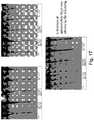
- Figure 2shows images of copper samples following laser treatment to form periodic structures on the surfaces of the samples as described in relation to Figure 1 .
- the operating parameters used in the laser treatment of the copper samplesare provided in the following table, Table 4. Three samples were treated, copper samples a), b) and c). Images of the samples a), b) and c), and four scanning electron microscope (SEM) images of the processed surfaces of samples, labelled 1 to 4, are shown in Figure 2 and described in Table 4 below.
- Figure 3shows images of aluminium samples following laser treatment to form periodic structures on the surface as described in relation to Figure 1 .
- the operating parameters used in the laser treatment of the aluminium samplesare provided in the following table, Table 5.
- Two sampleswere treated, aluminium samples a) and b). Images of the samples a) and b) and three scanning electron microscope (SEM) images of the processed surface of a sample at different levels of magnification, labelled 1 to 3, are shown in the figure and described in Table 5 below.
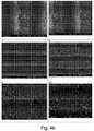
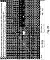
- Figures 4a and 4bshows images of stainless steel samples following laser treatment to form periodic structures on the surface as described in relation to Figure 1 .
- the operating parameters used in the laser treatment of the samplesare provided in the following tables, Tables 6a and 6b.
- Four sampleswere treated, stainless steel samples a), b), c) and d). Images of the samples a), b), c) and d) and scanning electron microscope (SEM) images of the processed surfaces of the samples, labelled 1 to 10, are shown in Figures 4a and 4b and described in Tables 6a and 6b below.
- the sampleswere referred to by the references PS10HDS (picosecond pulsed laser treatment), PS15HDS (picosecond pulsed laser treatment), PS15HD+ (picosecond pulsed laser treatment), NSHS (nanosecond pulsed laser treatment providing fluence of 4.8 GW/cm 2 ), and NSPS (nanosecond pulsed laser treatment providing fluence of 5.5 GW/cm 2 ).
- PS10HDSpicosecond pulsed laser treatment
- PS15HDSpicosecond pulsed laser treatment
- PS15HD+picosecond pulsed laser treatment
- NSHSnanosecond pulsed laser treatment providing fluence of 4.8 GW/cm 2
- NSPSnanosecond pulsed laser treatment providing fluence of 5.5 GW/cm 2
- the sampleswere samples of 316LN steel that were laser-processed using the parameters as set out in the table.
- NSHSDstainless steel sample referred to as NSHSD was also processed.
- the same processing parameterswere used for the NSHSD sample as for the NSHS sample, as provided in Tables 7 and 8, except that the laser writing was unidirectional rather than bidirectional. In an example of bidirectional writing the laser writes a line from (say) left to right and then the next line is from right to left. In an example of unidirectional writing the laser writes a line from, say, left to right and then the next line is also from left to right. Further parameters for the NSPS, NSHS and NSHSD samples are provided in Table 8 below.
- Each of the PS10HDS, PS15HDS, PS15HD+, NSHS, NSPS, and NSHD sampleswere of diameter 20 mm, and emissivity measurements were performed on the samples. The samples were stored in silk paper in a plastic box prior to the measurements being performed. Emissivity measurements were also performed on two stainless steel samples (of stainless steel type 304LN and 316LN) referred to as the 304LN and 316LN samples, that were not subject to laser processing and were used as reference samples.
- Figure 5presents emissivity measurement data for the NSHSD, NSHS and NSPS samples.
- the non-laser-processed 316LN and 304L reference samplesare also shown for comparison.
- the bottom two lines plotted on the graph of Figure 5represents the results of the emissivity measurements performed on the two untreated reference samples (the 304L and 316LN samples).
- the other linesrepresent measured emissivity as a function of wavelength for the laser treated NSHSD, NSHS and NSPS samples. More than one line is plotted for each of the NSHSD, NSHS and NSPS samples, representing measurements with different incident angles between incoming light and laser structures.
- the measured emissivities for the NSHSD and NSHS samplesare slightly lower compared to the measured emissivity for the NSPS sample at wavelengths shorter than 16 ⁇ m.
- the measured emissivitiesdo not depend on the angle of the incoming light with respect to the periodic structures formed by the laser processing.
- the NSPS samplehas the highest emissivity for wavelengths shorter than 16 ⁇ m.
- Results of emissivity measurements for the PS10HDS and PSA5HD+ samplesare shown in Figure 6 , together with the results for the NSPS sample and for the two non-laser-processed reference samples (316LN and 304L).
- the bottom two lines plotted on the graph of Figure 6represents the results of the emissivity measurements performed on the two untreated reference samples (the 304L and 316LN samples).
- the top group of linesrepresent results (also plotted in Figure 5 ) for the NSPS sample, representing measurements with different incident angles between incoming light and laser structures.
- the other two groups of linesrepresent measurements for the PS10HDS and PS15HD+ samples, the different lines in the groups representing measurements with different incident angles.
- the three different surface treatmentsare well distinguishable based on the emissivity measurements as a function of wavelength. All three laser-processed samples that are the subject of Figure 6 (the PS10HDS, PSA5HD+ and NSPS samples) show higher emissivities for all measured wavelengths than the non-laser-processed reference samples (304L and 316LN). Sample NSPS has the highest emissivity over the whole range.
- Figure 7shows SEM images of different positions on the surfaces of the laser-processed NSPS and NSHS samples.
- the processing parameters for the NSPS and NSHS sampleswere substantially the same except that the laser beam was scanned over the surface in a unidirectional fashion for the NSPS sample and in a bidirectional fashion for the NSHS sample.
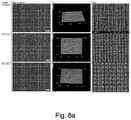
- Figures 8a and 8bshow 2d microscope images, 3d images and SEM images of the surfaces of the PS10HDS, PS15HDS, PS15HD+, NSHS and NSPS samples.
- Figure 9shows images of laser-processed aluminium samples labelled a) and b).
- Samples a) of Figure 9have a size 25 mm x 25 mm, thickness 1 mm.
- the laser-processed areaswere of area around 20 mm x 20 mm.
- the various samples a) of Figure 9were laser processed to form periodic structures using the following parameters: wavelength 532 nm; pulse duration 10 ps; repetition rate 200 kHZ; pulse energy range from 0.75 x10 -6 J to 29.8 x 10 -6 J; beam spot diameter approx.12 ⁇ m; scan speed from 5 mm/s to 15 mm/s; hatch distance range from 8 to 24 ⁇ m.
- Sample b) of Figure 9has a thickness of 1 mm and a laser-processed area of about 5 mm x 5 mm.
- Sample b) of Figure 9was laser processed to form periodic structures using the following parameters: wavelength 1064 nm; pulse duration 10 ps; repetition rate 200 kHZ; pulse energy 1.05 x 10 -6 J; beam spot diameter 16 ⁇ m; scan speed 10 mm/s; hatch distance 20 ⁇ m.
- Appendix 1provides further operating parameters of the laser to produce a desired periodic arrangement of structures on the surface according to further embodiments.
- Figure 10shows an image of a copper sample following laser treatment to form periodic structures (in this case cross-hatched structures) on the surface of the sample as described.
- periodic structuresin this case cross-hatched structures
- Five SEM images at five points (labelled 1, 3, 6, 9, 12) on the surfaceare also included in Figure 5 and show top-hat pyramid structures.
- Figure 11shows SEM images of further surfaces, labelled (a) to (e), following laser treatment to form periodic structures (in this case cross-hatched structures) on the surface of the sample as described.
- periodic structuresin this case cross-hatched structures
- Each different samplewas subject to pulses of a respective different power density as indicated in Figure 11 .
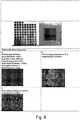
- Figure 12shows an image of a sample following laser treatment to form periodic structures (in this case parallel lines) on the surface of the sample. Five SEM images at five regions of the sample surface are also shown. The sample was subject to laser pulses of power density equal to 0.4 TW/cm 2 .
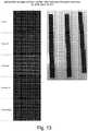
- Figure 13shows images of three samples following laser treatment to form periodic structures (in this case parallel lines) on the surface of the samples as described. Five SEM images at five regions of the surface of one of the samples are also shown. The sample was subject to laser pulses of power density equal to 0.2 TW/cm 2 .
- Figure 14shows an image of a copper sample, following laser treatment to form periodic structures on the surface as described.
- Figure 14also shows SEM images of regions of the surface at different magnifications.
- Figure 15shows SEM images, at various magnifications, of different regions of the surface of a copper sample, following laser treatment to form periodic structures on the surface as described.
- Figure 16shows SEM images at various magnifications of a cross-section of a copper sample following laser treatment to form periodic structures on the surface as described, and following cutting and polishing, together with a further image of the sample in face-on view.
- Figure 17shows SEM images of a cross-section of a copper sample at different regions of the sample, following laser treatment to form periodic structures on the surface,
- Figure 18shows images of a co-laminated sample comprising a copper layer on a stainless steel layer, following laser treatment to form periodic structures on the surface as described, and SEM images of cross-sections of the sample.
- Figure 19shows a further SEM image of a cross-section of a sample, following laser treatment to form periodic structures on the surface as described.
- Figure 20shows an SEM image of a sample in face-on view, following laser treatment to form periodic structures on the surface as described.
- An inset imageis included in the figure, and is an SEM cross-sectional image of a cross-section running along a line indicated in the face-on image. Corresponding positions on the face-on image and the cross-sectional image are marked with dots. There are three red dots (showing darker in black and white version of the figure) and one green dot (showing lighter in black and white version of the figure). The red dots indicate regions where the laser passed twice and the green dot indicates a region where the laser passed once. It can be seen in the cross-sectional image that two passes of the laser produced deeper valleys/troughs than one pass of the laser.
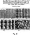
- Figure 21shows SEM images of a surface of a copper sample following laser treatment to form periodic structures on the surface as described.
- the laser treatmentused laser pulses of wavelength 532 nm and laser pulse power density of 29.6 GW/cm 2 .
- the laser pulseswere ps laser pulses and the power density was selected by selecting an appropriate laser spot size.
- Figure 22is an image of sample surfaces, including for the copper sample of Figure 21 .
- Figure 23shows an image of a surface of a sample following laser treatment to form periodic structures (in this case cross-hatching) on the surface as described.
- Figure 24shows an image of a surface of a sample following laser treatment to form periodic structures (in this case grooves) on the surface as described.
- Figure 25shows an image of a surface of a sample following laser treatment to form periodic structures (in this case cross-hatching) on the surface as described.
- Figure 26shows an image of a surface of a sample following laser treatment to form periodic structures (in this case grooves) on the surface as described.
- Figure 27shows further images of surfaces of samples following laser treatment to form periodic structures on the surface of the samples as described.
- Laser engineeringprovides an overarching methodology that provides for the formation of periodic structures according to embodiments, Precision laser engineering is expected to excite free electrons within metals, vibrations within insulators, and indeed both types of excitations within semiconductors.
- the mechanisms by which lasers can engineer materialsinclude the following:
- the focused laser beamacts as a spatially confined, intense heat source.
- Targeted materialis heated up rapidly, eventually causing it to be vaporized.
- the targeted materialcould be referred to as being boiled away.
- An advantage of this approachis that it may enable rapid removal of relatively large amount of target material.
- the peripheral heat affected zone (HAZ) damage and the presence of some recast material after processingpresent limitations in terms of heat confinement for precision laser materials engineering.
- the laserdrives multi-photon absorption of light inside the material. This strips electrons from the material, which then explode away due to Coulomb repulsion.
- PAIinvolves directly breaking the molecular or atomic bonds that hold the material together, rather than simply heating it, it is intrinsically not a 'hot' process. Since the material is removed in a very short timeframe, the ablated material carries away most of the energy before heat can spread into the surrounding material. These effects may result in a significantly reduced HAZ. Furthermore, this is a clean process and may leave minimal recast material, thereby eliminating the need for elaborate post-processing.
- the PAI mechanismis compatible with a very broad range of materials, including high band-gap materials that have low linear optical absorption and therefore are difficult to engineer with existing techniques.
- the PAI mechanismcan be considered 'wavelength neutral'; that is, nonlinear absorption can be reduced even if the material is normally transmissive at the laser wavelength.
- the PAI mechanismshould allow for custom design of electron work function of surfaces.
- the PTI and PAI mechanismare illustrated schematically in Figures 28a and 28b respectively.
- the characteristics of the pulsed radiation that is applied to the surfaceare such that the periodic structures that are formed are of shallower depth and/or more gently sloped than features formed using pulsed radiation of higher energy and/or longer duration for example pulse durations in the nano-second range.
- Using picosecond duration pulsed radiationcan in some cases also cause formation of nano-ripples or other small scale structures on the surface in addition to the larger scale peaks and troughs obtained by scanning the laser beam in an appropriate pattern over the surface. It is possible that such nano-ripples or other small scale structures may in some cases decrease the reflectivity of the surface further, in addition to the reduction obtained by larger periodic peak and trough structures. Furthermore, in some cases the nano-ripples or other small scale structures and/or the shallower peaks and troughs associate with picosecond rather than nanosecond pulses may also provide other improved or alternative properties of the surface, for example reduced induction, and/or can provide the surface with an increased area at the nano- or micro-scale.
Landscapes
- Physics & Mathematics (AREA)
- Optics & Photonics (AREA)
- Engineering & Computer Science (AREA)
- Plasma & Fusion (AREA)
- Mechanical Engineering (AREA)
- Laser Beam Processing (AREA)
- Radiation-Therapy Devices (AREA)
- Treatment Of Fiber Materials (AREA)
Description
- The present invention relates to a method of blackening a surface.
- Laser blackening of a surface may refer to the application of laser radiation to a surface to modify the surface so as to reduce the reflectivity of the surface, for example to reduce the reflectivity of the surface for visible light.
- There is a growing interest in marking of metals, for example in the creative industries or for security/identification applications. Laser marking is used widely in the manufacture of automotive steels, medical glasses, smartphone materials etc to create either a black or white mark.
US 2011/089039 describes techniques or processes for providing markings on products.Vorebyev A et al, "Colorizing Metals with Femtosecond Laser Pulses", Applied Physics Letters, vol. 92, no. 4, 31 January 2008, basis for the preamble ofclaim 1, describes femtosecond laser processing techniques for creating a variety of colors on a metal.US 2015/049593 describes a method of engraving a component involving application to the component of a laser beam the pulses of which each last less than one picosecond.US 2007/199927 describes laser-based methods and systems for removing one or more target link structures of a circuit fabricated on a substrate.- It is desired to provide improved or at least alternative methods for laser blackening of surfaces.
- A method of blackening a surface according to the present invention is defined in
claim 1, the method comprising: - applying laser radiation to the surface to produce a periodic arrangement of structures on the surface, wherein
- the laser radiation comprises pulsed laser radiation comprising a series of laser pulses and the power density of the pulses is in a range of 1 GW/cm2 to 50 GW/cm2;
- the laser radiation comprises a pulsed laser beam that has a focal spot diameter on the surface in a
range 1 µm to 100 µm and the pulsed radiation has a pulse repetition rate in arange 10 kHz to 1 MHz and an average power of the laser radiation is in a range 0.3 W to 20 W; - a pulse duration of the laser pulses is in a
range 200 femtoseconds (fs) to 1000 picoseconds (ps) or in a range 1000 ps to 200 ns;
and - the applying of the laser radiation to the surface comprises scanning the pulsed laser beam over the surface (10) such that the periodic arrangement of structures on the surface (10) comprises a periodic series of peaks and troughs substantially parallel to each other
- The use of such power densities may change the reflectivity or emissivity of the surface at visible or infrared wavelengths. The blackening may be at visible or infrared wavelengths, or at other suitable wavelengths of electro-magnetic radiation. Optionally at least some of the pulses may be interleaved with lower power laser pulses.
- Optionally the power density may be in a
range 1 GW/cm2 to 45 GW/cm2, optionally in arange 2 GW/cm2 to 30 GW/cm2, optionally in arange 4 GW/cm2 to 10 GW/cm2. - By using laser pulses having such power densities, a periodic arrangement of structures that provides a surface with desired properties may be obtained. For example a surface having a desired value or range of values of emissivity or reflectivity, or a desired blackening, at a wavelength or range of wavelengths of interest may be obtained.
- The laser pulses may have a duration less than a thermal relaxation time of the material of the surface. Alternatively the laser pulses may have a duration larger than the thermal relaxation time. The laser pulses may have a duration such that the electrons and the atomic lattice of the material of the surface have a substantially different temperature substantially throughout application of the laser pulses. The laser pulses may have a duration such that material of the surface is at least one of evaporated or vaporised or removed without substantial melting and/or flowing of the surface. The laser pulses may have a duration such that some material of the surface is at least one of evaporated or vaporised or removed without substantial melting and/or flowing of the remaining material of the surface.
- The peaks may be substantially flat on top and/or may be rounded on top and/or may have substantially no pointed and/or or sharp regions on top. The peaks may substantially have a top hat shape and/or a truncated pyramidal shape, for example a top hat shape and/or a truncated pyramidal shape in cross-sectional profile. Thus, for example, a desired value of electron work function and/or desired electron or photon trapping properties may be obtained. The peaks may extend in a longitudinal direction and may be referred to as ridges.
- The peak to trough distance for at least some of the peaks, and/or an average or median peak to trough distance, may be in a range 500 nm to 500 µm, optionally in a range 500 nm to 100 µm, optionally in a
range 100 µm to 500 µm, optionally in a range 5 µm to 100 µm, optionally in arange 20 µm to 80 µm, optionally in arange 1 µm to 60 µm, optionally in arange 30 µm to 60 µm. - The periodic arrangement of structures may comprise a cross-hatched arrangement or an arrangement of substantially parallel lines of peaks and troughs (for example, ridges and valleys) substantially without cross-hatching. The periodic arrangement of structures may, for example, be produced by a single pass of a laser source that provided the laser radiation.
- The surface may be on an at least one underlying layer (for example, at least one of steel, stainless steel) and the laser radiation may be such as to substantially not remove or move material of the surface in such a way as to expose the underlying layer.
- The method may be used to provide a laser treated surface comprising a laser-formed periodic arrangement of structures on the surface, wherein at least one of:
- the periodic arrangement of structures comprises a periodic series of peaks and troughs substantially parallel to each other;
- the periodic arrangement of structures comprises a cross-hatched, periodic series of peaks and troughs; and optionally
- the peaks may be substantially flat on top and/or may be rounded on top and/or may have substantially no pointed and/or or sharp regions on top and/or the peaks may substantially have a top hat shape and/or a truncated pyramidal shape, for example a top hat shape and/or a truncated pyramidal shape in cross-sectional profile; and/or
- the peak to trough distance for at least some of the peaks, and/or an average or median peak to trough distance, may be in a range 500 nm to 500 µm, optionally in a range 500 nm to 100 µm, optionally in a
range 100 µm to 500 µm, optionally in a range 5 µm to 100 µm, optionally in arange 20 µm to 80 µm, optionally in arange 1 µm to 60 µm, optionally in arange 30 µm to 60 µm. - The method may be performed using an apparatus that comprises:
- a laser source for applying pulsed laser radiation to a surface; and
- a laser controller configured to control the laser source to apply the laser radiation as a series of laser pulses thereby to form a periodic arrangement of structures on the surface, wherein the power density of the pulses is in a range of 1 GW/cm2 to 50 GW/cm2;
- wherein the laser radiation comprises a pulsed laser beam that has a focal spot diameter on the surface (10) in a
range 1 µm to 100 µm and the pulsed radiation has a pulse repetition rate in arange 10 kHz to 1 MHz and an average power of the laser radiation is in a range 0.3 W to 20 W; - a pulse duration of the laser pulses is in a
range 200 femtoseconds (fs) to 1000 picoseconds (ps) or in a range 1000 ps to 200 ns; and - the applying of the laser radiation to the surface comprises scanning the pulsed laser beam over the surface (10) such that the periodic arrangement of structures on the surface (10) comprises a periodic series of peaks and troughs substantially parallel to each other
- The surface may be the surface of a target.
- The pulse duration may be in a
range 1 ps to 100 ps or 1 ns to 100 ns. The pulse duration may be in arange 1 ps to 50 ps or 1 ns to 100 ns. The pulse duration may be in a range 5ps to 500 ps or 5 ns to 200 ns. - The laser radiation may comprise a pulsed laser beam that has a focal spot diameter on the surface in a
range 1 µm to 50 µm. - An average power of the laser radiation may be in a range 0.3 W to 20 W, or in a range 1 W to 5 W, or in a range 0.3W to 5W.
- A scan speed for the scanning may be in a
range 1 mm/s to 200 mm/s, optionally in arange 1 mm/s to 100 mm/s. - The scanning of the pulsed laser beam over the surface may be repeated between 2 and 20 times, or between 2 and 10 times, or may be performed once.
- An angle of incidence of the laser radiation to the surface may be in a range from 0 to 30 degrees. The angle of incidence of the laser radiation to the surface may be in a range from 90 degree to 60 degrees.
- A wavelength of the radiation may be in a
range 100 nm to 2,000 nm, optionally 532 nm or 528 nm or 1030 nm or 1064 nm or 1070 nm. - The periodic arrangement of structures may comprise a first series of peaks and troughs arranged in a first direction, and a second series of peaks and troughs arranged in a second, different direction. The first and second directions may be substantially orthogonal. The first series of peaks and troughs and the second series of peaks and troughs may intersect such that the periodic arrangement of structures comprises a cross-hatched arrangement.
- A period of the periodic arrangement may be in a range 0.5 µm to 100 µm. The separation of adjacent peaks (or troughs) of the periodic structure may be in a range 0.5 µm to 100 µm. A hatch distance of the cross-hatched arrangement may be in a range 0.5 µm to 100 µm.
- The surface may comprise or form part of a surface of, or a surface of a component of, for example, one or more of a computing device, an energy storage device, a communications device, a security device, a medical device, an identification device, a financial transaction device, an optical device, a storage device.
- The method may comprise applying the laser radiation to the surface to produce a periodic arrangement of structures on the surface over a selected area. The selected area may comprise or represent one or more of an image, an identifier, a marker. The marker may comprise a security marker.
- The method may comprise applying the laser radiation such as to produce the periodic arrangement of structures on the surface to form at least one of an image, an identifier, a marker, a security marker.
- The laser radiation may be such that the applying of the laser radiation to the surface comprises producing further structures. The further structures may be smaller than the structures of the periodic arrangement of structures.
- The further structures may comprise further periodic structures. The further structures may comprise ripples. The further structures may comprise nano-ripples. The further structures may be further periodic structures. The further structures may comprise laser induced periodic surface structures (LIPPS). The further structures may have a periodicity in a
range 10 nm to 1 µm, optionally in arange 100 nm to 1 µm. - The further structures may cover at least part of the periodic array of structures. The further structures may be formed in the troughs and/or on the peaks of the periodic arrangement of structures.
- The surface may be a metal surface. The surface and/or target may comprise copper, aluminium, stainless steel or titanium. The metal of the metal surface may be a metal selected from copper, aluminium, stainless steel, or titanium. The surface may form part of a laminated structure, for example a laminated target, for instance comprising one of copper, aluminium, stainless steel, titanium and at least one other material, and/or a laminated structure comprising at least two of copper, aluminium, stainless steel, titanium.
- The surface may be the surface of a foil. The target may be a foil.
- An average or peak fluence or other property of the laser radiation may be above an ablation threshold of the surface and within 100% to 300%, optionally 105%, optionally 102%, optionally 101% of the ablation threshold.
- The radiation may be such as to at least partially melt the surface and/or to provide flow of material at the surface.
- The pulses may be such that, for each pulse, a plasma is formed at the surface. The plasma may, for example, have substantially the same density as underlying material of the surface.
- The method may comprise applying the radiation using a solid-state laser, optionally the solid state laser comprises a Nd:YVO4 or Nd:YAG or Yb:YAG or Nd:KGW or Nd:KYW or Yb:KGW or Yb:KYW laser, or a pulsed fibre laser, optionally a Yb, Tm or Nd pulsed fibre laser. The applied radiation may comprise the fundamental wavelengths of operation such lasers or their second or third harmonics.
- The further structures may comprise further periodic structures. The further structures may comprise ripples. The further structures may comprise nano-ripples. The further structures may be further periodic structures. The further structures may comprise laser induced periodic surface structures (LIPPS). The further structures may have a periodicity in a
range 10 nm to 1 µm, optionally in arange 100 nm to 1 µm. - The structures may comprise peaks and troughs. The periodic arrangement of structures may comprise a periodic series of peaks and troughs. The peaks and troughs may be substantially parallel to each other.
- The periodic arrangement of structures may comprise a first series of peaks and troughs arranged in a first direction, and a second series of peaks and troughs arranged in a second, different direction. The first and second directions may be substantially orthogonal. The first series of peaks and troughs and the second series of peaks and troughs may intersect such that the periodic arrangement of structures comprises a cross-hatched arrangement.
- A period of the periodic arrangement may be in a range 0.5 µm to 100 µm or may be in a
range 100 µm to 500 µm. The separation of adjacent peaks (or troughs) of the periodic structure may be in a range 0.5 µm to 100 µm. A hatch distance of the cross-hatched arrangement may be in a range 0.5 µm to 100 µm. - The further structures may comprise further periodic structures. The further structures may comprise ripples. The further structures may comprise nano-ripples. The further structures may be further periodic structures. The further structures may comprise laser induced periodic surface structures (LIPPS). The further structures may have a periodicity in a
range 10 nm to 1 µm, optionally in arange 100 nm to 1 µm. - The further structures may cover at least part of the periodic array of structures. The further structures may be formed in the troughs of the periodic arrangement of structures.
- The surface may comprise or form part of a surface of, or a surface of a component of, for example, one or more of a computing device, a communications device, a security device, a medical device, an identification device, a financial transaction device, an optical device, a storage device.
- The periodic arrangement of structures may be arranged on the surface over a selected area. The selected area may comprise or represent one or more of an image, an identifier, a marker. The marker may comprise a security marker.
- The surface may be a metal surface. The surface may comprise copper, aluminium, stainless steel or titanium. The metal of the metal surface may be selected from copper, aluminium, stainless steel, titanium. The surface may form part of a laminated structure, for example a laminated target, for instance comprising one of copper, aluminium, stainless steel, titanium and at least one other material, and/or a laminated structure comprising at least two of copper, aluminium, stainless steel, titanium.
- The method may be used to form a surface of a computing device, an energy storage device, a communications device, a security device, a medical device, an identification device, a financial transaction device, an optical device, or a storage device.
- The method may be use to form an image, an identifier, a marker, or a security marker on a surface of a computing device, a communications device, a security device, a medical device, an identification device, a financial transaction device, an optical device, or a storage device
- Any feature in any one aspect of the invention may be applied to any other one or more of the aspects of the invention in any appropriate combination.
- Embodiments of the invention are further described hereinafter with reference to the accompanying drawings, in which:
Figure 1 is a schematic diagram of a system used for laser treatment of a surface to laser blacken the surface;Figure 2 shows images of copper samples following laser treatment to form periodic structures on the surfaces of the samples;Figure 3 shows images of aluminium samples following laser treatment to form periodic structures on the surfaces of the samples;Figures 4a and4b show images of stainless steel samples following laser treatment to form periodic structures on the surfaces of the samples;Figures 5 and6 are plots of emissivity as a function of wavelength for stainless steel samples following laser treatment to form periodic structures on the surfaces of the samples (demonstrating emissivity > 0.9 for wavelengths up to 30 µm, and for stainless steel reference samples (emissivity less than 0.4);Figure 7 shows SEM images of different positions on the surfaces of laser-processed stainless steel samples;Figures 8a and8b show 2d microscope images, 3d images and SEM images of the surfaces of laser-processed stainless steel samples;Figure 9 shows images of laser-processed aluminium samples; andFigures 10 to 27 show images of further samples, following laser treatment to form periodic structures on the surfaces of the further samples; andFigures 28a and 28b are schematic illustrations of laser interaction mechanisms.Figure 1 shows a system used to perform a method of laser treatment of a surface to laser blacken the surface.- The
system 2 ofFigure 1 comprises alaser 6 connected to alaser controller 4 which is used to control operation of thelaser 6 to emit a pulsed laser radiation beam of desired characteristics. Thelaser 6 is aligned with atarget 10 such that operation of thelaser 6 under control of thelaser controller 4 forms periodic structures on the surface of the target. - The laser may be one of a Nd:YVO4 or Nd:YAG or Yb:YAG or Nd:KGW or Nd:KYW or Yb:KGW or Yb:KYW laser and the main operating wavelength or one of the second or third harmonics may be used. Alternatively the laser may be a pulsed fibre laser, for example a Yb, Tm or Nd pulsed fibre laser, and the main operating wavelength or one of the second or third harmonics may be used. Any other suitable laser may be used. In
Figure 1 , the wavelength of the pulsed laser radiation is 532 nm, but any other suitable wavelength can be used in other embodiments, for example 528 nm or 1030 m or 1064 nm or 1070 nm. - The controller may comprise a dedicated controller, or a suitably programmed computer. The controller may be implemented in software, hardware or any suitable combination of hardware and software. In some embodiments, the controller may comprise more ASICs (application specific integrated circuits) or FPGAs (field programmable gate arrays) or other suitable circuitry.
- In
Figure 1 , thetarget 10 andlaser 6 are located in air and the laser treatment of the surface is performed in air. Thetarget 10 andlaser 6 may be positioned in a sealable and/orpumpable chamber 8 that has an associated pump and/or gas supply, and the laser processing of the surface may be performed in vacuum or in desired gaseous conditions, for example in the presence of a selected reactive gas. Thechamber 8 is omitted in some cases. - In
Figure 1 , the target is a metal target comprising copper. Other targets, for example aluminium, stainless steel or titanium can be used. - In operation pulsed laser radiation of desired characteristics is scanned across the surface of the
target 10 by thelaser 6 under control of thelaser controller 4 to produce a periodic arrangement of structures on the surface. For example, in order to form peaks and troughs arranged in parallel rows, the laser beam may be scanned along parallel, spaced-apart paths across the surface to form parallel troughs separated by peaks. Any other suitable arrangements of structures can be formed by suitable scanning of the laser beam over the surface. The laser can be controlled to form the structures over a desired area. The desired area may comprise or represent, for example, one or more of an image, an identifier, a marker. The marker may, for instance, comprise a security marker. - Operating parameters of the laser, and certain equations linking such parameters, can be represented as follows,
Wavelength (λ) [m]
Repetition rate of the laser (γ) [Hz]
Pulse length of the laser (τ) [s]
Average power of the laser (Pavg) [W] -represents the energy flow over one period t
Energy per pulse (Ep) [J]
Fluence of the laser (F) [J/cm2]
Beam spot radius on the target (r) [m]
Beam spot area on the target (A=πr2)[m2]
Number of times surface of the target was scanned by the laser beam (N) dimensionless
Speed at which surface of the target was scanned by the laser beam (V) [m/s]
Number of pulses fired per each spot on the surface of the target (n) [dimensionless]
Time interval between the pulses -one period (t) [s]
Peak Power (Ppeak) [W] -defines the energy flow within asingle pulse
Power density or Intensity (I) [W/cm2]
Equations


- Suitable operating parameters can be selected, for example based on the equations and representations above, to obtain pulsed laser radiation of desired properties, for example a desired power density of the pulses.
- Table 1 provides operating parameters of the laser to produce a desired periodic arrangement of structures on the surface, where the surface is copper. Three sets of operating parameters are provided in table 1.
- The laser processing of the surface is performed in air in this case.
Table 1 Copper Wavelength, nm Pulse Width Range Focal Spot Diameter on the target, µm Rep. Rate of the laser, kHz Average Power, W Scan Speed, mm/s Repetition Number of the scans Hatch Distance, µm Fluence, J/cm2 (Number of pulses per spot) 532 ∼ 10ps 12 200 0.94 (range between 0.77 to 1.00) 10 1 24 4.16 (240) 532 ∼10ps 40 200 0.75 10 1 30 0.3 (800) 1064 ∼10ps 73 200 3.27 30 1 55 0.39 (487) - In some other cases where the target is copper, operating parameters are selected as follows:
- a) Wavelength of 532 nm; Pulse width of the laser: from 200 femtosecond to 200 picosecond; Focal spot diameter on the target: from 1 µm to 50 µm; Repetition rate of the laser from 10 kHz to 1 MHz; Average power from 0.3 W to 2W; Scan speeds of 1 mm/s to 100 mm/s; Repetition number of scans from 1 to 10; Hatch Distance from 0.5 µm to 100 µm; angle of incidence of the laser beam from 0 to 30 degrees.
- b) Wavelength of 1064 nm; Pulse width of the laser: from 200 femtosecond to 200 picosecond; Focal spot diameter on the target: from 1 µm to 50 µm; Repetition rate of the laser from 10 kHz to 1 MHz; Average power from 1 W to 5 W; Scan speeds of 1 mm/s to 100 mm/s; Repetition number of scans from 1 to 10; Hatch Distance from 0.5 µm to 100 µm; angle of incidence of the laser beam from 0 to 30 degrees.
- Table 2 provides operating parameters of the laser to produce a desired periodic arrangement of structures on the surface, where the surface is aluminium.
Table 2 Aluminium Wavelength, nm Pulse Width Range Focal Spot Diameter on the target, µm Rep. Rate of the laser, kHz Average Power, W Scan Speed, mm/s Repetition Number of the scans Hatch Distance, µm Fluence, J/cm2 (Number of pulses per spot) 1064 ∼ 10ps 12 200 0.21 10 1 20 0.93 (240) - When the target is aluminium, operating parameters are selected as follows:
- a) Wavelength of 1064 nm; Pulse width of the laser: from 200 femtosecond to 200 picosecond; Focal spot diameter on the target: from 1 µm to 50 µm; Repetition rate of the laser from 10 kHz to 1 MHz; Average power from 0.1 W to 1 W; Scan speeds of 1 mm/s to 100 mm/s; Repetition number of scans from 1 to 10; Hatch Distance from 0.5 µm to 100 µm; angle of incidence of the laser beam from 0 to 30 degrees.
- Table 3 provides operating parameters of the laser to produce a desired periodic arrangement of structures on the surface, where the surface is stainless steel.
Table 3 Stainless steel Wavelength, nm Pulse Width Range Focal Spot Diameter on the target, µm Rep. Rate of the laser, kHz Average Power, W Scan Speed, mm/s Repetition Number of the scans Hatch Distance, µm Fluence, J/cm2 (Number of pulses per spot) 532 ∼ 10ps 12 200 0.44 10 1 24 1.95 (240) - When target is stainless steel, operating parameters are selected as follows:
- a) Wavelength of 532 nm; Pulse width of the laser: from 200 femtosecond to 200 picosecond; Focal spot diameter on the target: from 1 µm to 50 µm; Repetition rate of the laser from 10 kHz to 1 MHz; Average power from 0.1 W to 2 W; Scan speeds of 1 mm/s to 100 mm/s; Repetition number of scans from 1 to 10; Hatch Distance from 0.5 µm to 100 µm.
- b) Wavelength of 1064 nm; Pulse width of the laser: from 200 femtosecond to 200 picosecond; Focal spot diameter on the target: from 1 µm to 50 µm; Repetition rate of the laser from 10 kHz to 1 MHz; Average power from 1 W to 5 W; Scan speeds of 1 mm/s to 100 mm/s; Repetition number of scans from 1 to 10; Hatch Distance from 0.5 µm to 100 µm; angle of incidence of the laser beam from 0 to 30 degrees.
- The power density (intensity) used for stainless steel may be selected to be in a range from 0.01 TW/cm2 to 1 TW/cm2, for example by suitable choice of wavelength and of other operating parameters such as those recited in paragraphs a) or b) above.
Figure 2 shows images of copper samples following laser treatment to form periodic structures on the surfaces of the samples as described in relation toFigure 1 . The operating parameters used in the laser treatment of the copper samples are provided in the following table, Table 4. Three samples were treated, copper samples a), b) and c). Images of the samples a), b) and c), and four scanning electron microscope (SEM) images of the processed surfaces of samples, labelled 1 to 4, are shown inFigure 2 and described in Table 4 below.Figure 3 shows images of aluminium samples following laser treatment to form periodic structures on the surface as described in relation toFigure 1 . The operating parameters used in the laser treatment of the aluminium samples are provided in the following table, Table 5. Two samples were treated, aluminium samples a) and b). Images of the samples a) and b) and three scanning electron microscope (SEM) images of the processed surface of a sample at different levels of magnification, labelled 1 to 3, are shown in the figure and described in Table 5 below.

Figures 4a and4b shows images of stainless steel samples following laser treatment to form periodic structures on the surface as described in relation toFigure 1 . The operating parameters used in the laser treatment of the samples are provided in the following tables, Tables 6a and 6b. Four samples were treated, stainless steel samples a), b), c) and d). Images of the samples a), b), c) and d) and scanning electron microscope (SEM) images of the processed surfaces of the samples, labelled 1 to 10, are shown inFigures 4a and4b and described in Tables 6a and 6b below.

- Further, stainless steel samples were laser processed by the apparatus of
Figure 1 in accordance with the operating parameters provided in Table 7 below.Table 7 Name SE2c SE3c SE4c SE5c SE6c PS10HDS PS15HDS PS15HD+ NSHS NSPS λ [nm] 532 532 532 1064 1064 τ [s] 10p 10p 10p 10n 10n Rep rate [kHz] 200 200 200 20 20 Power setting 93% att 93% att 93% att 40% 38% Power [W] 0.2 0.2 0.2 2.7 3.1 Spot Ø [µm] 12 12 12 60 60 Pulse energy [µJ] 1.00 1.00 1.00 135.00 155.00 Fluence [J/cm2] 0.88 0.88 0.88 4.77 5.48 Structure [cross, line] cross cross cross cross cross Hatch Distance [µm] 10 15 20 50 75 Scan speed [mm/s] 10 10 10 10 10 Passes 1 1 1 1 10 Pulses/spot/pass 240 240 240 120 120 - The samples were referred to by the references PS10HDS (picosecond pulsed laser treatment), PS15HDS (picosecond pulsed laser treatment), PS15HD+ (picosecond pulsed laser treatment), NSHS (nanosecond pulsed laser treatment providing fluence of 4.8 GW/cm2), and NSPS (nanosecond pulsed laser treatment providing fluence of 5.5 GW/cm2). The samples were samples of 316LN steel that were laser-processed using the parameters as set out in the table.
- A further stainless steel sample referred to as NSHSD was also processed. The same processing parameters were used for the NSHSD sample as for the NSHS sample, as provided in Tables 7 and 8, except that the laser writing was unidirectional rather than bidirectional. In an example of bidirectional writing the laser writes a line from (say) left to right and then the next line is from right to left. In an example of unidirectional writing the laser writes a line from, say, left to right and then the next line is also from left to right. Further parameters for the NSPS, NSHS and NSHSD samples are provided in Table 8 below.
Table 8 Name NSPS NSHS NSHSD λ [nm] 1064 1064 τ [s] 10n 10n Rep rate [kHz] 20 20 Power setting 38% 40% Power [W] 2.7 3.1 Spot Ø [µm] 60 60 Pulse energy [µJ] 135.00 155.00 Fluence [J/cm2] 4.77 5.48 Structure [cross, line] cross cross Writing direction bidirectional bidirectional unidirectional Hatch Distance [µm] 75 50 Scan speed [mm/s] 10 10 Passes 10 1 Pulses/spot/pass 120 120 area width [mm] 12000 12000 area height [mm] 1000 1000 Process time [min] 5333333.33 800000.00 [d] 3703.703704 555.555556 - Each of the PS10HDS, PS15HDS, PS15HD+, NSHS, NSPS, and NSHD samples were of
diameter 20 mm, and emissivity measurements were performed on the samples. The samples were stored in silk paper in a plastic box prior to the measurements being performed. Emissivity measurements were also performed on two stainless steel samples (of stainless steel type 304LN and 316LN) referred to as the 304LN and 316LN samples, that were not subject to laser processing and were used as reference samples. - The emissivity of the samples was measured using infra-red light with wavelength from 2.5 µm to 25 µm. Each sample was measured several times turning it randomly to measure at different incidence angles (incident light in respect to the laser structure).
Figure 5 presents emissivity measurement data for the NSHSD, NSHS and NSPS samples. The non-laser-processed 316LN and 304L reference samples are also shown for comparison. - The bottom two lines plotted on the graph of
Figure 5 represents the results of the emissivity measurements performed on the two untreated reference samples (the 304L and 316LN samples). The other lines represent measured emissivity as a function of wavelength for the laser treated NSHSD, NSHS and NSPS samples. More than one line is plotted for each of the NSHSD, NSHS and NSPS samples, representing measurements with different incident angles between incoming light and laser structures. - As can be seen from
Figure 5 , the measured emissivities for the NSHSD and NSHS samples are slightly lower compared to the measured emissivity for the NSPS sample at wavelengths shorter than 16 µm. The measured emissivities do not depend on the angle of the incoming light with respect to the periodic structures formed by the laser processing. The NSPS sample has the highest emissivity for wavelengths shorter than 16 µm. - Results of emissivity measurements for the PS10HDS and PSA5HD+ samples are shown in
Figure 6 , together with the results for the NSPS sample and for the two non-laser-processed reference samples (316LN and 304L). The bottom two lines plotted on the graph ofFigure 6 represents the results of the emissivity measurements performed on the two untreated reference samples (the 304L and 316LN samples). The top group of lines represent results (also plotted inFigure 5 ) for the NSPS sample, representing measurements with different incident angles between incoming light and laser structures. The other two groups of lines represent measurements for the PS10HDS and PS15HD+ samples, the different lines in the groups representing measurements with different incident angles. - As can be seen from
Figure 6 , the three different surface treatments (for the PS10HDS, PSA5HD+ and NSPS samples) are well distinguishable based on the emissivity measurements as a function of wavelength. All three laser-processed samples that are the subject ofFigure 6 (the PS10HDS, PSA5HD+ and NSPS samples) show higher emissivities for all measured wavelengths than the non-laser-processed reference samples (304L and 316LN). Sample NSPS has the highest emissivity over the whole range. Figure 7 shows SEM images of different positions on the surfaces of the laser-processed NSPS and NSHS samples. The processing parameters for the NSPS and NSHS samples were substantially the same except that the laser beam was scanned over the surface in a unidirectional fashion for the NSPS sample and in a bidirectional fashion for the NSHS sample.Figures 8a and8b show 2d microscope images, 3d images and SEM images of the surfaces of the PS10HDS, PS15HDS, PS15HD+, NSHS and NSPS samples.Figure 9 shows images of laser-processed aluminium samples labelled a) and b).- Samples a) of
Figure 9 have a size 25 mm x 25 mm,thickness 1 mm. The laser-processed areas were of area around 20 mm x 20 mm. The various samples a) ofFigure 9 were laser processed to form periodic structures using the following parameters:wavelength 532 nm;pulse duration 10 ps;repetition rate 200 kHZ; pulse energy range from 0.75 x10⁻⁶ J to 29.8 x 10⁻⁶ J; beam spot diameter approx.12 µm; scan speed from 5 mm/s to 15 mm/s; hatch distance range from 8 to 24 µm. - Sample b) of
Figure 9 has a thickness of 1 mm and a laser-processed area of about 5 mm x 5 mm. Sample b) ofFigure 9 was laser processed to form periodic structures using the following parameters:wavelength 1064 nm;pulse duration 10 ps;repetition rate 200 kHZ; pulse energy 1.05 x 10⁻⁶ J;beam spot diameter 16 µm;scan speed 10 mm/s;hatch distance 20 µm. - SEM images of regions of the surface of sample b) are also shown in
Figure 9 , for different magnifications. Appendix 1 provides further operating parameters of the laser to produce a desired periodic arrangement of structures on the surface according to further embodiments.Figure 10 shows an image of a copper sample following laser treatment to form periodic structures (in this case cross-hatched structures) on the surface of the sample as described. Five SEM images at five points (labelled 1, 3, 6, 9, 12) on the surface are also included inFigure 5 and show top-hat pyramid structures.Figure 11 shows SEM images of further surfaces, labelled (a) to (e), following laser treatment to form periodic structures (in this case cross-hatched structures) on the surface of the sample as described. Each different sample was subject to pulses of a respective different power density as indicated inFigure 11 .Figure 12 shows an image of a sample following laser treatment to form periodic structures (in this case parallel lines) on the surface of the sample. Five SEM images at five regions of the sample surface are also shown. The sample was subject to laser pulses of power density equal to 0.4 TW/cm2.Figure 13 shows images of three samples following laser treatment to form periodic structures (in this case parallel lines) on the surface of the samples as described. Five SEM images at five regions of the surface of one of the samples are also shown. The sample was subject to laser pulses of power density equal to 0.2 TW/cm2.Figure 14 shows an image of a copper sample, following laser treatment to form periodic structures on the surface as described.Figure 14 also shows SEM images of regions of the surface at different magnifications.Figure 15 shows SEM images, at various magnifications, of different regions of the surface of a copper sample, following laser treatment to form periodic structures on the surface as described.Figure 16 shows SEM images at various magnifications of a cross-section of a copper sample following laser treatment to form periodic structures on the surface as described, and following cutting and polishing, together with a further image of the sample in face-on view.Figure 17 shows SEM images of a cross-section of a copper sample at different regions of the sample, following laser treatment to form periodic structures on the surface,Figure 18 shows images of a co-laminated sample comprising a copper layer on a stainless steel layer, following laser treatment to form periodic structures on the surface as described, and SEM images of cross-sections of the sample.Figure 19 shows a further SEM image of a cross-section of a sample, following laser treatment to form periodic structures on the surface as described.Figure 20 shows an SEM image of a sample in face-on view, following laser treatment to form periodic structures on the surface as described. An inset image is included in the figure, and is an SEM cross-sectional image of a cross-section running along a line indicated in the face-on image. Corresponding positions on the face-on image and the cross-sectional image are marked with dots. There are three red dots (showing darker in black and white version of the figure) and one green dot (showing lighter in black and white version of the figure). The red dots indicate regions where the laser passed twice and the green dot indicates a region where the laser passed once. It can be seen in the cross-sectional image that two passes of the laser produced deeper valleys/troughs than one pass of the laser.Figure 21 shows SEM images of a surface of a copper sample following laser treatment to form periodic structures on the surface as described. The laser treatment used laser pulses ofwavelength 532 nm and laser pulse power density of 29.6 GW/cm2. The laser pulses were ps laser pulses and the power density was selected by selecting an appropriate laser spot size.Figure 22 is an image of sample surfaces, including for the copper sample ofFigure 21 .Figure 23 shows an image of a surface of a sample following laser treatment to form periodic structures (in this case cross-hatching) on the surface as described.Figure 24 shows an image of a surface of a sample following laser treatment to form periodic structures (in this case grooves) on the surface as described.Figure 25 shows an image of a surface of a sample following laser treatment to form periodic structures (in this case cross-hatching) on the surface as described.Figure 26 shows an image of a surface of a sample following laser treatment to form periodic structures (in this case grooves) on the surface as described.Figure 27 shows further images of surfaces of samples following laser treatment to form periodic structures on the surface of the samples as described.- Without wishing to be bound by theory, and without limitation to the scope of protection, the following comments are provided which relate to processes which may occur in relation to some cases.
- Laser engineering provides an overarching methodology that provides for the formation of periodic structures according to embodiments, Precision laser engineering is expected to excite free electrons within metals, vibrations within insulators, and indeed both types of excitations within semiconductors. The mechanisms by which lasers can engineer materials include the following:
- (i) Photo-thermal interaction (PTI) - commonly achieved using laser beams providing short dwell time (e.g. lasers with nanosecond pulsewidth);
- (ii) Photo-ablation interaction (PAI) - envisaged using laser beams providing ultra-short dwell time (e.g. lasers with picosecond or femtosecond pulsewidth).
- In the PTI regime the focused laser beam acts as a spatially confined, intense heat source. Targeted material is heated up rapidly, eventually causing it to be vaporized. Without wishing to imply any limitation to the scope of protection, the targeted material could be referred to as being boiled away. An advantage of this approach is that it may enable rapid removal of relatively large amount of target material. However, the peripheral heat affected zone (HAZ) damage and the presence of some recast material after processing present limitations in terms of heat confinement for precision laser materials engineering.
- In the PAI regime, the laser drives multi-photon absorption of light inside the material. This strips electrons from the material, which then explode away due to Coulomb repulsion. Because PAI involves directly breaking the molecular or atomic bonds that hold the material together, rather than simply heating it, it is intrinsically not a 'hot' process. Since the material is removed in a very short timeframe, the ablated material carries away most of the energy before heat can spread into the surrounding material. These effects may result in a significantly reduced HAZ. Furthermore, this is a clean process and may leave minimal recast material, thereby eliminating the need for elaborate post-processing. The PAI mechanism is compatible with a very broad range of materials, including high band-gap materials that have low linear optical absorption and therefore are difficult to engineer with existing techniques. The PAI mechanism can be considered 'wavelength neutral'; that is, nonlinear absorption can be reduced even if the material is normally transmissive at the laser wavelength.
- The PAI mechanism should allow for custom design of electron work function of surfaces.
- The PTI and PAI mechanism are illustrated schematically in
Figures 28a and 28b respectively. - It is a further feature that the characteristics of the pulsed radiation that is applied to the surface, for example the use of pulse durations in the picosecond range or less, are such that the periodic structures that are formed are of shallower depth and/or more gently sloped than features formed using pulsed radiation of higher energy and/or longer duration for example pulse durations in the nano-second range.
- Again, without wishing to be bound by theory, and without limitation to the scope of protection, the following comments are provided which relate to processes which may occur in relation to some cases.
- In irradiation at very high intensities (or high irradiance) one is confronted with the issue of a dense, strongly absorbing material, in the first few tens of nm of which energy at a rate of some 1020 W/cm3 is liberated. Part of this energy, once randomised, is conducted into the bulk of the material, while part is converted into directed kinetic energy by thermal expansion of the heated layer. Two regimes are distinguished in this respect.
- 1. Nanosecond pulsed laser interaction which is dominated by the expansion and ablation of material. Here the thermal pressure of the heated layer is sufficient to cause significant compression of the underlying target material.
- 2. Picosecond pulsed laser interaction which is heat conduction dominated since hydrodynamic motion during the pulse duration is negligible (laser pulses here may be 1000 times or more shorter than nanosecond ones). An important point here is that in the picosecond regime the strong heating of the dense material occurs before hydrodynamic expansion of the processed layer has even started. The plasmas produced in this regime have essentially the same density as the solid target itself. This - upon cooling - leads to the formation of fine structures - in the range from 1 micrometres to 50 micrometres depending on the irradiation parameters - covered with nano-structures.
- Using picosecond duration pulsed radiation can in some cases also cause formation of nano-ripples or other small scale structures on the surface in addition to the larger scale peaks and troughs obtained by scanning the laser beam in an appropriate pattern over the surface. It is possible that such nano-ripples or other small scale structures may in some cases decrease the reflectivity of the surface further, in addition to the reduction obtained by larger periodic peak and trough structures. Furthermore, in some cases the nano-ripples or other small scale structures and/or the shallower peaks and troughs associate with picosecond rather than nanosecond pulses may also provide other improved or alternative properties of the surface, for example reduced induction, and/or can provide the surface with an increased area at the nano- or micro-scale.
- It will be understood that the present invention has been described above purely by way of example, and modifications of detail can be made within the scope of the present invention as defined in the appended claims.


Claims (10)
- A method of blackening a surface (10), comprising:applying laser radiation to the surface to produce a periodic arrangement of structures on the surface,the method beingcharacterised in that:the laser radiation comprises pulsed laser radiation comprising a series of laser pulses and the power density of the pulses is in a range 1 GW/cm2 to 50 GW/cm2;the laser radiation comprises a pulsed laser beam that has a focal spot diameter on the surface in a range 1 µm to 100 µm and the pulsed radiation has a pulse repetition rate in a range 10 kHz to 1 MHz and an average power of the laser radiation is in a range 0.3 W to 20 W;a pulse duration of the laser pulses is in a range 200 femtoseconds (fs) to 1000 picoseconds (ps) or in a range 1000 ps to 200 ns;
andthe applying of the laser radiation to the surface comprises scanning the pulsed laser beam over the surface (10) such that the periodic arrangement of structures on the surface (10) comprises a periodic series of peaks and troughs substantially parallel to each other. - The method according to claim 1, wherein at least some of the laser pulses have a duration less than a thermal relaxation time of the material of the surface (10).
- The method according to claim 1 or 2, wherein the peaks are substantially flat on top and/or are rounded on top and/or have substantially no pointed and/or or sharp regions on top.
- The method according to any preceding claim, wherein the peak to trough distance for at least some of the peaks, and/or an average or median peak to trough distance, is in a range 5 µm to 100 µm, optionally in a range 20 µm to 80 µm, optionally in a range 30 µm to 60 µm.
- The method according to any preceding claim, wherein at least one of a) or b):a) the periodic arrangement of structures comprises a cross-hatched arrangement or an arrangement of substantially parallel lines of peaks and troughs substantially without cross-hatching;b) the method comprises performing a single pass of the laser source across the surface (10) to produce the periodic arrangement of structures.
- The method according to any preceding claim, wherein at least one of c) to f):c) a scan speed for the scanning is in a range 1 mm/s to 200 mm/s;d) the scanning of the pulsed laser beam over the surface (10) is repeated between 2 and 10 times, or is performed once;e) an angle of incidence of the laser radiation to the surface (10) is in a range from 0 to 30 degrees or from 90 degree to 60 degrees;f) a wavelength of the radiation is in a range 100 nm to 2,000 nm, optionally 532 nm or 528 nm or 1030 nm or 1064 nm or 1070 nm.
- The method according to any preceding claim, wherein the applying of the laser radiation to the surface (10) is such as to produce further structures, and the further structures are smaller than the structures of said periodic arrangement of structures.
- The method according to Claim 7, wherein at least one of j) to m):j) the further structures comprise further periodic structures, optionally ripples or nano-ripples;k) the further structures comprise laser induced periodic surface structures (LIPPS);l) the further structures have a periodicity in a range 10 nm to 1 µm, optionally in a range 100 nm to 1 µm;m) the further structures cover at least part of the periodic array of structures and/or are formed in the troughs and/or on the peaks of the periodic arrangement of structures.
- The method according to any preceding claim, wherein at least one of n) to q):n) the surface (10) comprises a metal surface, optionally a copper, aluminium, stainless steel or titanium surface;o) the surface comprises or forms part of one or more of a computing device, a communications device, a security device, a medical device, an identification device, a financial transaction device, an optical device, a storage device;p) the method comprises applying the laser radiation such as to produce the periodic arrangement of structures on the surface over a selected area, wherein the selected area comprises or represents one or more of an image, an identifier, a marker, a security marker;q) the method comprises applying the laser radiation such as to produce the periodic arrangement of structures on the surface to form at least one of an image, an identifier, a marker, a security marker.
- The method according to any preceding claim, comprising applying the radiation using a solid-state laser (6), optionally the solid state laser comprises a Nd:YVO4 or Nd:YAG or Yb:YAG or Nd:KGW or Nd:KYW or Yb:KGW or Yb:KYW laser, or a pulsed fibre laser, optionally a Yb, Tm or Nd pulsed fibre laser, optionally wherein applying the radiation comprises using the fundamental wavelength of operation of the laser or its second or third harmonic.
Applications Claiming Priority (6)
| Application Number | Priority Date | Filing Date | Title |
|---|---|---|---|
| GBGB1511154.5AGB201511154D0 (en) | 2015-06-24 | 2015-06-24 | Method of, and apparatus for, reducing photoelectron yield and/or secondary elecctron yield |
| GBGB1511153.7AGB201511153D0 (en) | 2015-06-24 | 2015-06-24 | Method of, an apparatus for laser blackening of a surface |
| GBGB1517235.6AGB201517235D0 (en) | 2015-09-30 | 2015-09-30 | Method of, and apparatus for, reducing photoelectron yield and/or secondary electron yield |
| GBGB1517232.3AGB201517232D0 (en) | 2015-09-30 | 2015-09-30 | Method of, and apparatus for, reducing photoelectron yield and/or secondary electron yield |
| GBGB1603991.9AGB201603991D0 (en) | 2016-03-08 | 2016-03-08 | Processing method and apparatus |
| PCT/GB2016/051908WO2016207659A1 (en) | 2015-06-24 | 2016-06-24 | Method of, and apparatus for, laser blackening of a surface, wherein the laser has a specific power density and/or a specific pulse duration |
Publications (2)
| Publication Number | Publication Date |
|---|---|
| EP3313605A1 EP3313605A1 (en) | 2018-05-02 |
| EP3313605B1true EP3313605B1 (en) | 2021-01-27 |
Family
ID=56411814
Family Applications (2)
| Application Number | Title | Priority Date | Filing Date |
|---|---|---|---|
| EP16738849.5AActiveEP3313605B1 (en) | 2015-06-24 | 2016-06-24 | Method of laser blackening of a surface, wherein the laser has a specific power density and a specific pulse duration |
| EP16741107.3AActiveEP3313606B1 (en) | 2015-06-24 | 2016-06-24 | Method of reducing photoelectron yield and/or secondary electron yield using laser beam radiation |
Family Applications After (1)
| Application Number | Title | Priority Date | Filing Date |
|---|---|---|---|
| EP16741107.3AActiveEP3313606B1 (en) | 2015-06-24 | 2016-06-24 | Method of reducing photoelectron yield and/or secondary electron yield using laser beam radiation |
Country Status (10)
| Country | Link |
|---|---|
| US (2) | US11033985B2 (en) |
| EP (2) | EP3313605B1 (en) |
| JP (2) | JP2018519165A (en) |
| KR (2) | KR20180055798A (en) |
| CN (2) | CN108260349B (en) |
| AU (1) | AU2016283066A1 (en) |
| BR (2) | BR112017027953A2 (en) |
| CA (2) | CA3002318A1 (en) |
| RU (2) | RU2018102525A (en) |
| WO (2) | WO2016207660A1 (en) |
Families Citing this family (19)
| Publication number | Priority date | Publication date | Assignee | Title |
|---|---|---|---|---|
| RU2018102525A (en)* | 2015-06-24 | 2019-07-24 | Юниверсити Оф Данди | METHOD AND DEVICE FOR LASER SURFACE BLACKING |
| GB201603991D0 (en)* | 2016-03-08 | 2016-04-20 | Univ Dundee | Processing method and apparatus |
| JP6781092B2 (en)* | 2017-03-29 | 2020-11-04 | 日本ピラー工業株式会社 | Coating base material |
| DE102017112613B4 (en)* | 2017-06-08 | 2020-10-01 | Olympus Winter & Ibe Gmbh | Process for blackening a diaphragm, blackened diaphragm, optical system and endoscope with such a diaphragm |
| WO2019166836A1 (en) | 2018-02-28 | 2019-09-06 | Foundation For Research And Technology Hellas | Using lasers to reduce reflection of transparent solids, coatings and devices employing transparent solids |
| DE102018105845A1 (en)* | 2018-03-14 | 2019-09-19 | Olympus Winter & Ibe Gmbh | Holder for an optical system of an endoscope and method for producing a holder for an optical system of an endoscope |
| KR102186568B1 (en)* | 2018-11-08 | 2020-12-03 | 한국생산기술연구원 | Color implementing method of metal surface and surface color implemented metal panel |
| DE102018128843A1 (en) | 2018-11-16 | 2020-05-20 | Dr. Ing. H.C. F. Porsche Aktiengesellschaft | Process for creating an ornament in a clear lacquer layer |
| FR3092588B1 (en)* | 2019-02-11 | 2022-01-21 | Radiall Sa | Anti-multipactor coating deposited on an RF or MW metal component, Process for producing such a coating by laser texturing. |
| JP7328835B2 (en)* | 2019-03-04 | 2023-08-17 | 株式会社東芝 | Welding method |
| EP4023590A4 (en)* | 2019-08-29 | 2023-09-13 | University Public Corporation Osaka | Photothermal conversion element, production method for same, photothermal power generation device, and micro-object aggregation system |
| CN112705862B (en)* | 2019-10-25 | 2023-05-26 | 大族激光科技产业集团股份有限公司 | Blackening treatment method and system for transparent PC (polycarbonate) piece based on ultrafast laser |
| CN111076818A (en)* | 2019-12-02 | 2020-04-28 | 中国航空工业集团公司北京长城计量测试技术研究所 | Preparation method of high-temperature surface source radiation source |
| US12057608B2 (en)* | 2020-03-10 | 2024-08-06 | Reinz-Dichtungs-Gmbh | Separator plate with periodic surface structures in the nanometer to micrometer range |
| JP7749942B2 (en)* | 2020-08-20 | 2025-10-07 | 株式会社リコー | Pattern Forming Device |
| CN112091419B (en)* | 2020-09-17 | 2022-03-29 | 吉林大学 | Based on hundred TW/cm2Method for efficiently preparing flexible pressure sensor template by using magnitude high-intensity laser |
| US20220143748A1 (en)* | 2020-11-12 | 2022-05-12 | Nutech Ventures | Laser surface processing systems and methods for producing near perfect hemispherical emissivity in metallic surfaces |
| CN114473212B (en)* | 2022-03-11 | 2023-02-03 | 北京理工大学 | Pyrolytic carbon surface self-organizing three-level micro-nano composite structure |
| KR20250036595A (en) | 2023-09-07 | 2025-03-14 | 한국생산기술연구원 | Method for controlling metal surface blackening through beam shaping of ultrashort pulse laser |
Family Cites Families (53)
| Publication number | Priority date | Publication date | Assignee | Title |
|---|---|---|---|---|
| JPS4834667A (en)* | 1971-09-08 | 1973-05-21 | ||
| JPH0640797A (en) | 1992-04-23 | 1994-02-15 | Sumitomo Electric Ind Ltd | Diamond processing method |
| JPH05325780A (en)* | 1992-05-14 | 1993-12-10 | Nec Corp | Manufacture of collector electrode for microwave tube |
| US6518540B1 (en) | 1998-06-16 | 2003-02-11 | Data Storage Institute | Method and apparatus for providing ablation-free laser marking on hard disk media |
| JP4115051B2 (en)* | 1998-10-07 | 2008-07-09 | キヤノン株式会社 | Electron beam equipment |
| US7838794B2 (en) | 1999-12-28 | 2010-11-23 | Gsi Group Corporation | Laser-based method and system for removing one or more target link structures |
| US6407363B2 (en)* | 2000-03-30 | 2002-06-18 | Electro Scientific Industries, Inc. | Laser system and method for single press micromachining of multilayer workpieces |
| JP4578710B2 (en)* | 2001-03-28 | 2010-11-10 | 独立行政法人科学技術振興機構 | Method of creating domain-inverted structure by femtosecond laser irradiation |
| GB0112234D0 (en) | 2001-05-18 | 2001-07-11 | Welding Inst | Surface modification |
| JP2003303561A (en)* | 2002-04-10 | 2003-10-24 | Canon Inc | Spacer, method of manufacturing spacer, and electron beam device |
| US9409254B2 (en) | 2005-09-30 | 2016-08-09 | Lawrence Livermore National Security, Llc | Ablation layers to prevent pitting in laser peening |
| US8846551B2 (en) | 2005-12-21 | 2014-09-30 | University Of Virginia Patent Foundation | Systems and methods of laser texturing of material surfaces and their applications |
| US7628865B2 (en)* | 2006-04-28 | 2009-12-08 | Asml Netherlands B.V. | Methods to clean a surface, a device manufacturing method, a cleaning assembly, cleaning apparatus, and lithographic apparatus |
| US20080299408A1 (en) | 2006-09-29 | 2008-12-04 | University Of Rochester | Femtosecond Laser Pulse Surface Structuring Methods and Materials Resulting Therefrom |
| US20080216926A1 (en) | 2006-09-29 | 2008-09-11 | Chunlei Guo | Ultra-short duration laser methods for the nanostructuring of materials |
| WO2008091898A1 (en)* | 2007-01-23 | 2008-07-31 | Imra America, Inc. | Ultrashort laser micro-texture printing |
| MX2009013616A (en) | 2007-06-12 | 2010-06-01 | Technolines Llc | High speed and high power laser scribing methods and systems. |
| US20100040836A1 (en)* | 2008-08-12 | 2010-02-18 | Shenping Li | Method for providing sub-surface marks in polymeric materials |
| JP2010050138A (en)* | 2008-08-19 | 2010-03-04 | Canon Machinery Inc | Method of forming minute cyclic structure |
| CN101368256A (en)* | 2008-10-17 | 2009-02-18 | 北京工业大学 | A Method of Using Ultrashort Pulse Laser to Change the Color of Metal Surface |
| US20110183111A1 (en) | 2008-10-22 | 2011-07-28 | Toyo Seikan Kaisha, Ltd. | Laminated structural body having a fine periodic structure |
| US8663754B2 (en)* | 2009-03-09 | 2014-03-04 | Imra America, Inc. | Pulsed laser micro-deposition pattern formation |
| US9993895B2 (en) | 2009-03-30 | 2018-06-12 | Boegli-Gravures Sa | Method and device for structuring the surface of a hard material coated solid body by means of a laser |
| US20110089039A1 (en)* | 2009-10-16 | 2011-04-21 | Michael Nashner | Sub-Surface Marking of Product Housings |
| EP2336810A1 (en) | 2009-12-18 | 2011-06-22 | Boegli-Gravures S.A. | Method and device for generating colour patterns using a diffraction grating |
| US8451873B2 (en) | 2010-02-11 | 2013-05-28 | Electro Scientific Industries, Inc. | Method and apparatus for reliably laser marking articles |
| US8379678B2 (en) | 2010-02-11 | 2013-02-19 | Electro Scientific Industries, Inc. | Method and apparatus for reliably laser marking articles |
| US8743165B2 (en) | 2010-03-05 | 2014-06-03 | Micronic Laser Systems Ab | Methods and device for laser processing |
| EP2553403B1 (en) | 2010-03-30 | 2019-02-20 | Sun Chemical Corporation | Reversible piezochromic system and method of making a reversible piezochromic system |
| US8389895B2 (en) | 2010-06-25 | 2013-03-05 | Electro Scientifix Industries, Inc. | Method and apparatus for reliably laser marking articles |
| JP6121901B2 (en) | 2010-07-12 | 2017-04-26 | ロフィン−シナー テクノロジーズ インコーポレーテッド | Material processing by laser filament formation |
| GB201011720D0 (en) | 2010-07-13 | 2010-08-25 | Univ Southampton | Controlling the colours of metals: bas-relief and intaglio metamaterials |
| RU2447012C1 (en) | 2010-10-28 | 2012-04-10 | Российская Федерация, от имени которой выступает Министерство промышленности и торговли Российской Федерации (Минпромторг России) | Method of producing steel nanostructured surface by laser-induced plasma processing |
| KR20140044299A (en)* | 2011-03-10 | 2014-04-14 | 일렉트로 싸이언티픽 인더스트리이즈 인코포레이티드 | Method and apparatus for reliably laser marking articles |
| US20130083500A1 (en)* | 2011-09-30 | 2013-04-04 | Christopher D. Prest | Interferometric color marking |
| JP2013111595A (en)* | 2011-11-28 | 2013-06-10 | Shin Etsu Polymer Co Ltd | Method of processing metal mold and method of forming emblem |
| JP6254540B2 (en) | 2012-03-12 | 2017-12-27 | ロレックス・ソシエテ・アノニムRolex Sa | Clock element engraving method and clock element obtained by the method |
| PL222531B1 (en) | 2012-04-05 | 2016-08-31 | Wrocławskie Centrum Badań Eit + Spółka Z Ograniczoną | Method and system for color marking of metals |
| US20140083984A1 (en) | 2012-09-23 | 2014-03-27 | Timothy Gerke | Formation Of Laser Induced Periodic Surface Structures (LIPSS) With Picosecond Pulses |
| FR2996487B1 (en) | 2012-10-08 | 2014-11-28 | Snecma | SURFACE MARKING METHOD OF A GAS TURBINE ENGINE PART BY A PREFINED GRAPHICAL REPRESENTATION |
| GB201221184D0 (en) | 2012-11-24 | 2013-01-09 | Spi Lasers Uk Ltd | Method for laser marking a metal surface with a desired colour |
| CN104884205A (en)* | 2012-12-20 | 2015-09-02 | 伊雷克托科学工业股份有限公司 | Methods of forming images by laser micromachining |
| US9413137B2 (en) | 2013-03-15 | 2016-08-09 | Nlight, Inc. | Pulsed line beam device processing systems using laser diodes |
| JP6079505B2 (en) | 2013-08-26 | 2017-02-15 | 三菱マテリアル株式会社 | Bonded body and power module substrate |
| CN103586578B (en) | 2013-11-14 | 2016-08-31 | 苏州图森激光有限公司 | A kind of material surface laser melanism or color method |
| FR3019074B1 (en) | 2014-04-01 | 2016-04-15 | Snecma | METHOD FOR SURFACE MARKING A MECHANICAL PIECE BY PREDEFINED GRAPHICAL REPRESENTATION WITH HOLOGRAPHIC TYPE EFFECT |
| GB2527291B (en) | 2014-06-13 | 2021-01-13 | Res & Innovation Uk | Apparatus and methods relating to reduced photoelectron yield and/or secondary electron yield |
| ES2564054B1 (en) | 2014-09-16 | 2016-12-27 | Consejo Superior De Investigaciones Científicas (Csic) | Anti-multipactor coating |
| WO2016159933A1 (en) | 2015-03-27 | 2016-10-06 | Siemens Aktiengesellschaft | Hybrid ceramic matrix composite components for gas turbines |
| EP3031785B1 (en) | 2014-12-12 | 2018-10-17 | Schott AG | Method for producing a glass ceramic element having a structured coating |
| CN104741852B (en) | 2015-03-19 | 2016-05-25 | 江苏大学 | A kind of deck of ship soldering test adjustable clamp |
| CN107532272B (en) | 2015-04-21 | 2020-04-17 | 东华隆株式会社 | Method for roughening surface of substrate, method for treating surface of substrate, spray-coated member, and method for producing same |
| RU2018102525A (en) | 2015-06-24 | 2019-07-24 | Юниверсити Оф Данди | METHOD AND DEVICE FOR LASER SURFACE BLACKING |
- 2016
- 2016-06-24RURU2018102525Apatent/RU2018102525A/ennot_activeApplication Discontinuation
- 2016-06-24AUAU2016283066Apatent/AU2016283066A1/ennot_activeAbandoned
- 2016-06-24JPJP2017566325Apatent/JP2018519165A/enactivePending
- 2016-06-24BRBR112017027953Apatent/BR112017027953A2/ennot_activeIP Right Cessation
- 2016-06-24CACA3002318Apatent/CA3002318A1/ennot_activeAbandoned
- 2016-06-24JPJP2017566333Apatent/JP2018524182A/enactivePending
- 2016-06-24USUS15/739,062patent/US11033985B2/ennot_activeExpired - Fee Related
- 2016-06-24EPEP16738849.5Apatent/EP3313605B1/enactiveActive
- 2016-06-24CNCN201680046529.4Apatent/CN108260349B/ennot_activeExpired - Fee Related
- 2016-06-24BRBR112017027975Apatent/BR112017027975A2/ennot_activeApplication Discontinuation
- 2016-06-24CACA3002315Apatent/CA3002315A1/ennot_activeAbandoned
- 2016-06-24KRKR1020187002213Apatent/KR20180055798A/ennot_activeWithdrawn
- 2016-06-24EPEP16741107.3Apatent/EP3313606B1/enactiveActive
- 2016-06-24WOPCT/GB2016/051909patent/WO2016207660A1/ennot_activeCeased
- 2016-06-24CNCN201680046220.5Apatent/CN108235694B/ennot_activeExpired - Fee Related
- 2016-06-24USUS15/739,074patent/US10807197B2/ennot_activeExpired - Fee Related
- 2016-06-24KRKR1020187002203Apatent/KR20180055797A/ennot_activeWithdrawn
- 2016-06-24RURU2018102523Apatent/RU2018102523A/ennot_activeApplication Discontinuation
- 2016-06-24WOPCT/GB2016/051908patent/WO2016207659A1/ennot_activeCeased
Non-Patent Citations (1)
| Title |
|---|
| None* |
Also Published As
| Publication number | Publication date |
|---|---|
| CA3002318A1 (en) | 2016-12-29 |
| CN108235694A (en) | 2018-06-29 |
| BR112017027975A2 (en) | 2018-08-28 |
| CN108260349A (en) | 2018-07-06 |
| EP3313606B1 (en) | 2020-03-25 |
| US11033985B2 (en) | 2021-06-15 |
| KR20180055798A (en) | 2018-05-25 |
| CN108235694B (en) | 2020-08-21 |
| US10807197B2 (en) | 2020-10-20 |
| JP2018519165A (en) | 2018-07-19 |
| US20180185958A1 (en) | 2018-07-05 |
| WO2016207660A1 (en) | 2016-12-29 |
| CA3002315A1 (en) | 2016-12-29 |
| JP2018524182A (en) | 2018-08-30 |
| AU2016283066A1 (en) | 2018-02-08 |
| RU2018102525A3 (en) | 2019-12-24 |
| KR20180055797A (en) | 2018-05-25 |
| RU2018102525A (en) | 2019-07-24 |
| US20180178319A1 (en) | 2018-06-28 |
| EP3313605A1 (en) | 2018-05-02 |
| BR112017027953A2 (en) | 2018-08-28 |
| RU2018102523A (en) | 2019-07-25 |
| RU2018102523A3 (en) | 2019-12-24 |
| EP3313606A1 (en) | 2018-05-02 |
| WO2016207659A1 (en) | 2016-12-29 |
| CN108260349B (en) | 2020-07-03 |
Similar Documents
| Publication | Publication Date | Title |
|---|---|---|
| EP3313605B1 (en) | Method of laser blackening of a surface, wherein the laser has a specific power density and a specific pulse duration | |
| Domke et al. | Surface ablation efficiency and quality of fs lasers in single-pulse mode, fs lasers in burst mode, and ns lasers | |
| EP3169475B1 (en) | Method and device for the laser-based working of two-dimensional, crystalline substrates, in particular semiconductor substrates | |
| US20210053160A1 (en) | Method and System for Ultrafast Laser-based Material Removal, Figuring and Polishing | |
| Knowles et al. | Micro-machining of metals, ceramics and polymers using nanosecond lasers | |
| Neuenschwander et al. | Processing of metals and dielectric materials with ps-laserpulses: results, strategies, limitations and needs | |
| KR20130059337A (en) | Laser-based material processing apparatus and methods | |
| EP3335826A1 (en) | Laser based hole formation and etching of transparent materials | |
| Lopez et al. | Comparison of picosecond and femtosecond laser ablation for surface engraving of metals and semiconductors | |
| WO2005115678A1 (en) | Method and device for cutting through semiconductor materials | |
| EP3511106A1 (en) | Laser based machining of glass material | |
| EP3789157A1 (en) | Method for treating the surface of a solid object | |
| CN109070266B (en) | Method for reducing the photoelectron yield and/or secondary electron yield of a ceramic surface; corresponding apparatus and products | |
| Karkantonis et al. | Femtosecond Laser Drilling of High-Density Micro-Holes on Metals Using MHz Burst Mode | |
| DE102005055174B3 (en) | Removing material by laser beam involves using a fluid containing metal or metal alloy to contact side of transparent material which is opposite incoming laser beam | |
| Ulmeanu et al. | Selective removal and patterning of a Co/Cu/Co trilayer created by femtosecond laser processing | |
| Baskevicius et al. | Optimization of Laser-Ablation Micromachining by Choice of Scanning Algorithms and Use of Laser-Induced-Breakdown Spectroscopy | |
| JP2024093854A (en) | Laser processing equipment and laser processing method | |
| DE102022122965A1 (en) | Creating dimples on the surface of a transparent material | |
| WO2021151789A2 (en) | Method and device for machining a metal workpiece | |
| Nogueira et al. | Study of ablation on surfaces of nuclear-use metals irradiated with Femtosecond laser | |
| Bauer et al. | Influence of Pulse Duration on the Glass Cutting Process | |
| EP2690073A1 (en) | Method for manufacturing a domestic appliance and domestic appliance | |
| Hendow | Effects of peak power and multipulsing on drilling and marking with ns pulses |
Legal Events
| Date | Code | Title | Description |
|---|---|---|---|
| STAA | Information on the status of an ep patent application or granted ep patent | Free format text:STATUS: THE INTERNATIONAL PUBLICATION HAS BEEN MADE | |
| PUAI | Public reference made under article 153(3) epc to a published international application that has entered the european phase | Free format text:ORIGINAL CODE: 0009012 | |
| STAA | Information on the status of an ep patent application or granted ep patent | Free format text:STATUS: REQUEST FOR EXAMINATION WAS MADE | |
| 17P | Request for examination filed | Effective date:20180124 | |
| AK | Designated contracting states | Kind code of ref document:A1 Designated state(s):AL AT BE BG CH CY CZ DE DK EE ES FI FR GB GR HR HU IE IS IT LI LT LU LV MC MK MT NL NO PL PT RO RS SE SI SK SM TR | |
| AX | Request for extension of the european patent | Extension state:BA ME | |
| DAV | Request for validation of the european patent (deleted) | ||
| DAX | Request for extension of the european patent (deleted) | ||
| STAA | Information on the status of an ep patent application or granted ep patent | Free format text:STATUS: EXAMINATION IS IN PROGRESS | |
| 17Q | First examination report despatched | Effective date:20190221 | |
| GRAP | Despatch of communication of intention to grant a patent | Free format text:ORIGINAL CODE: EPIDOSNIGR1 | |
| STAA | Information on the status of an ep patent application or granted ep patent | Free format text:STATUS: GRANT OF PATENT IS INTENDED | |
| INTG | Intention to grant announced | Effective date:20200819 | |
| GRAS | Grant fee paid | Free format text:ORIGINAL CODE: EPIDOSNIGR3 | |
| GRAA | (expected) grant | Free format text:ORIGINAL CODE: 0009210 | |
| STAA | Information on the status of an ep patent application or granted ep patent | Free format text:STATUS: THE PATENT HAS BEEN GRANTED | |
| AK | Designated contracting states | Kind code of ref document:B1 Designated state(s):AL AT BE BG CH CY CZ DE DK EE ES FI FR GB GR HR HU IE IS IT LI LT LU LV MC MK MT NL NO PL PT RO RS SE SI SK SM TR | |
| REG | Reference to a national code | Ref country code:GB Ref legal event code:FG4D | |
| REG | Reference to a national code | Ref country code:CH Ref legal event code:EP | |
| REG | Reference to a national code | Ref country code:AT Ref legal event code:REF Ref document number:1357894 Country of ref document:AT Kind code of ref document:T Effective date:20210215 | |
| REG | Reference to a national code | Ref country code:IE Ref legal event code:FG4D | |
| REG | Reference to a national code | Ref country code:DE Ref legal event code:R096 Ref document number:602016052065 Country of ref document:DE | |
| REG | Reference to a national code | Ref country code:NL Ref legal event code:MP Effective date:20210127 | |
| REG | Reference to a national code | Ref country code:LT Ref legal event code:MG9D | |
| REG | Reference to a national code | Ref country code:AT Ref legal event code:MK05 Ref document number:1357894 Country of ref document:AT Kind code of ref document:T Effective date:20210127 | |
| PG25 | Lapsed in a contracting state [announced via postgrant information from national office to epo] | Ref country code:LT Free format text:LAPSE BECAUSE OF FAILURE TO SUBMIT A TRANSLATION OF THE DESCRIPTION OR TO PAY THE FEE WITHIN THE PRESCRIBED TIME-LIMIT Effective date:20210127 Ref country code:BG Free format text:LAPSE BECAUSE OF FAILURE TO SUBMIT A TRANSLATION OF THE DESCRIPTION OR TO PAY THE FEE WITHIN THE PRESCRIBED TIME-LIMIT Effective date:20210427 Ref country code:PT Free format text:LAPSE BECAUSE OF FAILURE TO SUBMIT A TRANSLATION OF THE DESCRIPTION OR TO PAY THE FEE WITHIN THE PRESCRIBED TIME-LIMIT Effective date:20210527 Ref country code:NO Free format text:LAPSE BECAUSE OF FAILURE TO SUBMIT A TRANSLATION OF THE DESCRIPTION OR TO PAY THE FEE WITHIN THE PRESCRIBED TIME-LIMIT Effective date:20210427 Ref country code:FI Free format text:LAPSE BECAUSE OF FAILURE TO SUBMIT A TRANSLATION OF THE DESCRIPTION OR TO PAY THE FEE WITHIN THE PRESCRIBED TIME-LIMIT Effective date:20210127 Ref country code:HR Free format text:LAPSE BECAUSE OF FAILURE TO SUBMIT A TRANSLATION OF THE DESCRIPTION OR TO PAY THE FEE WITHIN THE PRESCRIBED TIME-LIMIT Effective date:20210127 Ref country code:GR Free format text:LAPSE BECAUSE OF FAILURE TO SUBMIT A TRANSLATION OF THE DESCRIPTION OR TO PAY THE FEE WITHIN THE PRESCRIBED TIME-LIMIT Effective date:20210428 | |
| PG25 | Lapsed in a contracting state [announced via postgrant information from national office to epo] | Ref country code:SE Free format text:LAPSE BECAUSE OF FAILURE TO SUBMIT A TRANSLATION OF THE DESCRIPTION OR TO PAY THE FEE WITHIN THE PRESCRIBED TIME-LIMIT Effective date:20210127 Ref country code:AT Free format text:LAPSE BECAUSE OF FAILURE TO SUBMIT A TRANSLATION OF THE DESCRIPTION OR TO PAY THE FEE WITHIN THE PRESCRIBED TIME-LIMIT Effective date:20210127 Ref country code:LV Free format text:LAPSE BECAUSE OF FAILURE TO SUBMIT A TRANSLATION OF THE DESCRIPTION OR TO PAY THE FEE WITHIN THE PRESCRIBED TIME-LIMIT Effective date:20210127 Ref country code:RS Free format text:LAPSE BECAUSE OF FAILURE TO SUBMIT A TRANSLATION OF THE DESCRIPTION OR TO PAY THE FEE WITHIN THE PRESCRIBED TIME-LIMIT Effective date:20210127 Ref country code:PL Free format text:LAPSE BECAUSE OF FAILURE TO SUBMIT A TRANSLATION OF THE DESCRIPTION OR TO PAY THE FEE WITHIN THE PRESCRIBED TIME-LIMIT Effective date:20210127 | |
| PG25 | Lapsed in a contracting state [announced via postgrant information from national office to epo] | Ref country code:IS Free format text:LAPSE BECAUSE OF FAILURE TO SUBMIT A TRANSLATION OF THE DESCRIPTION OR TO PAY THE FEE WITHIN THE PRESCRIBED TIME-LIMIT Effective date:20210527 | |
| REG | Reference to a national code | Ref country code:DE Ref legal event code:R097 Ref document number:602016052065 Country of ref document:DE | |
| PG25 | Lapsed in a contracting state [announced via postgrant information from national office to epo] | Ref country code:EE Free format text:LAPSE BECAUSE OF FAILURE TO SUBMIT A TRANSLATION OF THE DESCRIPTION OR TO PAY THE FEE WITHIN THE PRESCRIBED TIME-LIMIT Effective date:20210127 Ref country code:CZ Free format text:LAPSE BECAUSE OF FAILURE TO SUBMIT A TRANSLATION OF THE DESCRIPTION OR TO PAY THE FEE WITHIN THE PRESCRIBED TIME-LIMIT Effective date:20210127 Ref country code:SM Free format text:LAPSE BECAUSE OF FAILURE TO SUBMIT A TRANSLATION OF THE DESCRIPTION OR TO PAY THE FEE WITHIN THE PRESCRIBED TIME-LIMIT Effective date:20210127 | |
| PG25 | Lapsed in a contracting state [announced via postgrant information from national office to epo] | Ref country code:DK Free format text:LAPSE BECAUSE OF FAILURE TO SUBMIT A TRANSLATION OF THE DESCRIPTION OR TO PAY THE FEE WITHIN THE PRESCRIBED TIME-LIMIT Effective date:20210127 Ref country code:SK Free format text:LAPSE BECAUSE OF FAILURE TO SUBMIT A TRANSLATION OF THE DESCRIPTION OR TO PAY THE FEE WITHIN THE PRESCRIBED TIME-LIMIT Effective date:20210127 Ref country code:RO Free format text:LAPSE BECAUSE OF FAILURE TO SUBMIT A TRANSLATION OF THE DESCRIPTION OR TO PAY THE FEE WITHIN THE PRESCRIBED TIME-LIMIT Effective date:20210127 | |
| PLBE | No opposition filed within time limit | Free format text:ORIGINAL CODE: 0009261 | |
| STAA | Information on the status of an ep patent application or granted ep patent | Free format text:STATUS: NO OPPOSITION FILED WITHIN TIME LIMIT | |
| REG | Reference to a national code | Ref country code:DE Ref legal event code:R119 Ref document number:602016052065 Country of ref document:DE | |
| 26N | No opposition filed | Effective date:20211028 | |
| PG25 | Lapsed in a contracting state [announced via postgrant information from national office to epo] | Ref country code:AL Free format text:LAPSE BECAUSE OF FAILURE TO SUBMIT A TRANSLATION OF THE DESCRIPTION OR TO PAY THE FEE WITHIN THE PRESCRIBED TIME-LIMIT Effective date:20210127 Ref country code:MC Free format text:LAPSE BECAUSE OF FAILURE TO SUBMIT A TRANSLATION OF THE DESCRIPTION OR TO PAY THE FEE WITHIN THE PRESCRIBED TIME-LIMIT Effective date:20210127 Ref country code:ES Free format text:LAPSE BECAUSE OF FAILURE TO SUBMIT A TRANSLATION OF THE DESCRIPTION OR TO PAY THE FEE WITHIN THE PRESCRIBED TIME-LIMIT Effective date:20210127 | |
| REG | Reference to a national code | Ref country code:CH Ref legal event code:PL | |
| GBPC | Gb: european patent ceased through non-payment of renewal fee | Effective date:20210624 | |
| PG25 | Lapsed in a contracting state [announced via postgrant information from national office to epo] | Ref country code:SI Free format text:LAPSE BECAUSE OF FAILURE TO SUBMIT A TRANSLATION OF THE DESCRIPTION OR TO PAY THE FEE WITHIN THE PRESCRIBED TIME-LIMIT Effective date:20210127 | |
| REG | Reference to a national code | Ref country code:BE Ref legal event code:MM Effective date:20210630 | |
| PG25 | Lapsed in a contracting state [announced via postgrant information from national office to epo] | Ref country code:LU Free format text:LAPSE BECAUSE OF NON-PAYMENT OF DUE FEES Effective date:20210624 | |
| PG25 | Lapsed in a contracting state [announced via postgrant information from national office to epo] | Ref country code:LI Free format text:LAPSE BECAUSE OF NON-PAYMENT OF DUE FEES Effective date:20210630 Ref country code:IT Free format text:LAPSE BECAUSE OF FAILURE TO SUBMIT A TRANSLATION OF THE DESCRIPTION OR TO PAY THE FEE WITHIN THE PRESCRIBED TIME-LIMIT Effective date:20210127 Ref country code:IE Free format text:LAPSE BECAUSE OF NON-PAYMENT OF DUE FEES Effective date:20210624 Ref country code:GB Free format text:LAPSE BECAUSE OF NON-PAYMENT OF DUE FEES Effective date:20210624 Ref country code:DE Free format text:LAPSE BECAUSE OF NON-PAYMENT OF DUE FEES Effective date:20220101 Ref country code:CH Free format text:LAPSE BECAUSE OF NON-PAYMENT OF DUE FEES Effective date:20210630 | |
| PG25 | Lapsed in a contracting state [announced via postgrant information from national office to epo] | Ref country code:IS Free format text:LAPSE BECAUSE OF FAILURE TO SUBMIT A TRANSLATION OF THE DESCRIPTION OR TO PAY THE FEE WITHIN THE PRESCRIBED TIME-LIMIT Effective date:20210527 Ref country code:FR Free format text:LAPSE BECAUSE OF NON-PAYMENT OF DUE FEES Effective date:20210630 | |
| PG25 | Lapsed in a contracting state [announced via postgrant information from national office to epo] | Ref country code:BE Free format text:LAPSE BECAUSE OF NON-PAYMENT OF DUE FEES Effective date:20210630 | |
| PG25 | Lapsed in a contracting state [announced via postgrant information from national office to epo] | Ref country code:NL Free format text:LAPSE BECAUSE OF NON-PAYMENT OF DUE FEES Effective date:20210127 Ref country code:CY Free format text:LAPSE BECAUSE OF FAILURE TO SUBMIT A TRANSLATION OF THE DESCRIPTION OR TO PAY THE FEE WITHIN THE PRESCRIBED TIME-LIMIT Effective date:20210127 | |
| PG25 | Lapsed in a contracting state [announced via postgrant information from national office to epo] | Ref country code:HU Free format text:LAPSE BECAUSE OF FAILURE TO SUBMIT A TRANSLATION OF THE DESCRIPTION OR TO PAY THE FEE WITHIN THE PRESCRIBED TIME-LIMIT; INVALID AB INITIO Effective date:20160624 | |
| PG25 | Lapsed in a contracting state [announced via postgrant information from national office to epo] | Ref country code:MK Free format text:LAPSE BECAUSE OF FAILURE TO SUBMIT A TRANSLATION OF THE DESCRIPTION OR TO PAY THE FEE WITHIN THE PRESCRIBED TIME-LIMIT Effective date:20210127 | |
| PG25 | Lapsed in a contracting state [announced via postgrant information from national office to epo] | Ref country code:MT Free format text:LAPSE BECAUSE OF FAILURE TO SUBMIT A TRANSLATION OF THE DESCRIPTION OR TO PAY THE FEE WITHIN THE PRESCRIBED TIME-LIMIT Effective date:20210127 |