EP3293880A1 - Adaptation circuit for low noise amplifier and low noise amplifier including such a circuit - Google Patents
Adaptation circuit for low noise amplifier and low noise amplifier including such a circuitDownload PDFInfo
- Publication number
- EP3293880A1 EP3293880A1EP17189319.1AEP17189319AEP3293880A1EP 3293880 A1EP3293880 A1EP 3293880A1EP 17189319 AEP17189319 AEP 17189319AEP 3293880 A1EP3293880 A1EP 3293880A1
- Authority
- EP
- European Patent Office
- Prior art keywords
- frequency
- impedance
- terminal
- connection port
- circuit
- Prior art date
- Legal status (The legal status is an assumption and is not a legal conclusion. Google has not performed a legal analysis and makes no representation as to the accuracy of the status listed.)
- Granted
Links
- 230000006978adaptationEffects0.000titleclaimsdescription29
- 239000002887superconductorSubstances0.000claimsabstractdescription15
- 239000003990capacitorSubstances0.000claimsdescription13
- 239000000463materialSubstances0.000claimsdescription8
- 230000010287polarizationEffects0.000claimsdescription4
- 239000012212insulatorSubstances0.000claimsdescription2
- 241000238366CephalopodaSpecies0.000claims1
- 230000003321amplificationEffects0.000description19
- 238000003199nucleic acid amplification methodMethods0.000description19
- 238000000034methodMethods0.000description11
- 230000008569processEffects0.000description11
- 230000008901benefitEffects0.000description5
- 238000006243chemical reactionMethods0.000description4
- 230000008878couplingEffects0.000description4
- 238000010168coupling processMethods0.000description4
- 238000005859coupling reactionMethods0.000description4
- 230000000694effectsEffects0.000description4
- XAGFODPZIPBFFR-UHFFFAOYSA-NaluminiumChemical compound[Al]XAGFODPZIPBFFR-UHFFFAOYSA-N0.000description3
- 229910052782aluminiumInorganic materials0.000description3
- CFJRGWXELQQLSA-UHFFFAOYSA-NazanylidyneniobiumChemical compound[Nb]#NCFJRGWXELQQLSA-UHFFFAOYSA-N0.000description3
- 235000021183entréeNutrition0.000description3
- 241000135309ProcessusSpecies0.000description2
- 238000010521absorption reactionMethods0.000description2
- 230000007423decreaseEffects0.000description2
- 238000004519manufacturing processMethods0.000description2
- RYGMFSIKBFXOCR-UHFFFAOYSA-NCopperChemical compound[Cu]RYGMFSIKBFXOCR-UHFFFAOYSA-N0.000description1
- 241000893313Helochara deltaSpecies0.000description1
- 230000003044adaptive effectEffects0.000description1
- 238000013459approachMethods0.000description1
- 230000005540biological transmissionEffects0.000description1
- 230000006835compressionEffects0.000description1
- 238000007906compressionMethods0.000description1
- 238000001816coolingMethods0.000description1
- 229910052802copperInorganic materials0.000description1
- 239000010949copperSubstances0.000description1
- 230000001419dependent effectEffects0.000description1
- 238000010790dilutionMethods0.000description1
- 239000012895dilutionSubstances0.000description1
- 238000009826distributionMethods0.000description1
- 238000004134energy conservationMethods0.000description1
- 230000004907fluxEffects0.000description1
- 229910052734heliumInorganic materials0.000description1
- 239000001307heliumSubstances0.000description1
- SWQJXJOGLNCZEY-UHFFFAOYSA-Nhelium atomChemical compound[He]SWQJXJOGLNCZEY-UHFFFAOYSA-N0.000description1
- 238000011065in-situ storageMethods0.000description1
- 230000001939inductive effectEffects0.000description1
- 239000007788liquidSubstances0.000description1
- 230000007246mechanismEffects0.000description1
- 238000005457optimizationMethods0.000description1
- 239000002245particleSubstances0.000description1
- 230000010363phase shiftEffects0.000description1
- 230000005610quantum mechanicsEffects0.000description1
- 230000002040relaxant effectEffects0.000description1
- 239000004065semiconductorSubstances0.000description1
- 239000000243solutionSubstances0.000description1
- 230000002269spontaneous effectEffects0.000description1
- 238000010626work up procedureMethods0.000description1
Images


Classifications
- H—ELECTRICITY
- H03—ELECTRONIC CIRCUITRY
- H03F—AMPLIFIERS
- H03F1/00—Details of amplifiers with only discharge tubes, only semiconductor devices or only unspecified devices as amplifying elements
- H03F1/56—Modifications of input or output impedances, not otherwise provided for
- H—ELECTRICITY
- H03—ELECTRONIC CIRCUITRY
- H03F—AMPLIFIERS
- H03F1/00—Details of amplifiers with only discharge tubes, only semiconductor devices or only unspecified devices as amplifying elements
- H03F1/56—Modifications of input or output impedances, not otherwise provided for
- H03F1/565—Modifications of input or output impedances, not otherwise provided for using inductive elements
- H—ELECTRICITY
- H03—ELECTRONIC CIRCUITRY
- H03F—AMPLIFIERS
- H03F19/00—Amplifiers using superconductivity effects
- H—ELECTRICITY
- H03—ELECTRONIC CIRCUITRY
- H03F—AMPLIFIERS
- H03F3/00—Amplifiers with only discharge tubes or only semiconductor devices as amplifying elements
- H03F3/189—High-frequency amplifiers, e.g. radio frequency amplifiers
- H03F3/19—High-frequency amplifiers, e.g. radio frequency amplifiers with semiconductor devices only
- H—ELECTRICITY
- H03—ELECTRONIC CIRCUITRY
- H03F—AMPLIFIERS
- H03F3/00—Amplifiers with only discharge tubes or only semiconductor devices as amplifying elements
- H03F3/60—Amplifiers in which coupling networks have distributed constants, e.g. with waveguide resonators
- H03F3/608—Reflection amplifiers, i.e. amplifiers using a one-port amplifying element and a multiport coupler
- H—ELECTRICITY
- H03—ELECTRONIC CIRCUITRY
- H03F—AMPLIFIERS
- H03F7/00—Parametric amplifiers
- H—ELECTRICITY
- H03—ELECTRONIC CIRCUITRY
- H03F—AMPLIFIERS
- H03F2200/00—Indexing scheme relating to amplifiers
- H03F2200/294—Indexing scheme relating to amplifiers the amplifier being a low noise amplifier [LNA]
- H—ELECTRICITY
- H03—ELECTRONIC CIRCUITRY
- H03F—AMPLIFIERS
- H03F2200/00—Indexing scheme relating to amplifiers
- H03F2200/387—A circuit being added at the output of an amplifier to adapt the output impedance of the amplifier
Definitions
- the technical field of the inventionis that of high frequency amplifiers.
- the present inventionrelates to an adaptation circuit for a low noise amplifier.
- the inventionalso relates to a low-noise amplifier comprising such a matching circuit and in particular a low-noise Josephson junction amplifier.
- phase-preserving amplifiersare not subject to theoretical limitation but they are difficult to use because the phase of the signal to be amplified must perfectly correspond to the amplified quadrature.
- Phase-preserving amplifiersare subject to the quantum limit but do not impose any condition on the phase of the signal to be amplified.
- reflection amplificationIn the field of high frequency and very high frequency amplification, it is known to use reflection amplification.
- the latteris obtained for example by means of an impedance transmission line Z 0 terminated by an impedance Z L (f) where f is the frequency of the signal.
- the frequency f 1is called the pump frequency f p
- the frequency f 2is called the signal frequency f s
- the frequency f 3is called the frequency idler f i . It is possible to obtain an amplification of a signal of frequency f s by the generation of other photons of frequency signal f s from the pump photons of frequency f p , this generation also causing the generation of photons idler of frequency f i . So that this process of amplification takes place, it is also necessary, in addition to the condition of energy conservation, that the different frequencies are coupled together. Such coupling is achieved using a non-linear impedance.
- the amplificationcan be achieved, in the simplest embodiment, with a single Josephson junction.
- a deviceis illustrated in figure 1 and consists of an adaptation circuit comprising a first connection port J1 and a second connection port J2, both of these ports being connected to a Josephson JJ junction.
- a voltage source Vis connected by means of a T-connection constituted by the inductance L 3 and the capacitance C 2 .
- the matching circuitalso comprises a resistor R 1 in series with a capacitance C 1 and an inductance L 1 in parallel with each other.
- This matching circuitallows a bias of the Josephson JJ junction so that the latter has a negative differential impedance over a wide voltage range while maintaining a global impedance, i.e., the impedance of the Josephson junction. JJ and adaptive circuit, positive.
- the Josephson junctionis short-circuited by the circuit adaptation.
- R 1being of the order of a few ohms against several tens of ohms for Z 0 , the real part of the reflection coefficient becomes Re (G (f)) ⁇ -1 and there is therefore no amplification of the signal but only a phase shift of ⁇ .
- the impedance of the matching circuitis high and the impedance of the Josephson junction JJ thus becomes "visible" so that the impedance measured at the input port / output is such that Z L ⁇ 0 and
- more Z L -Z approaches 0the more the amplification is large.
- the circuit L 2 C 2makes it possible to carry out an impedance matching between the impedance of the Josephson junction JJ at the frequency f s and the input port of the circuit.
- Inductance L 3makes it possible for it to isolate the high frequency part of the circuit of the DC part.
- this deviceimproves the noise compared to an amplifier using transistors, the noise level remains higher than the noise level obtained with a parametric amplifier.
- the inventionoffers a solution to the problems mentioned above by proposing an adaptation circuit making it possible to reduce the noise generated by a voltage-polarized Josephson junction amplifier. It also offers an amplifier using such a circuit.
- a first aspect of the inventionrelates to an impedance matching circuit intended to be connected to a non-linear impedance comprising a superconductor, said circuit comprising a first terminal said first connection port intended to be connected to a first terminal of the non-linear impedance, a second terminal said second connection port intended to be connected to a second terminal of the nonlinear impedance, a third terminal called input / output terminal for receiving the signal to be amplified with a power gain G and a bandwidth BW and a fourth terminal said power terminal to be connected to a bias source and configured so that a voltage V can be applied between the first connection port and the second connection port.
- Z (f x )is the value of the impedance for a frequency belonging to a frequency range of defined width and centered on the frequency f x .
- a frequency f xthe latter must be understood as a frequency f belonging to an interval [f x - ⁇ f, f x + ⁇ f] with ⁇ f ⁇ 0.5f s or even ⁇ f ⁇ 0.1 f s .
- the polarization sourcemay in particular be chosen from a voltage source, a current source or even a finite impedance.
- the probability that a Cooper pair will relax by generating a photon at the frequency fis approximately proportional to the impedance seen by the superconducting element at said frequency f.
- a pair of Cooperhas a greater probability of relaxing by emitting a photon at the frequency f when a resonance mode of the impedance Z (f) seen by the nonlinear impedance is present at this frequency.
- the inventors, taking advantage of this property,have identified the conditions concerning this impedance which limit the noise generated.
- Re Z f iavoids that photons at the signal frequency f s are converted, during the relaxation of the Cooper pairs, into photons at the pump frequency plus the signal frequency f p + f s , which would lead to the decrease of the signal ratio on noise, a part of the photons of the signal being lost during this conversion.
- photons of the signal signal signal f sto associate with photons of the pump frequency pump f p to create photons of pump frequency plus frequency signal f p + f s .
- the condition f i > k B T hmakes it possible to ensure that the frequency idler f i is not peopled with thermal photons.
- the temperature in question hereis the temperature of the element in which the photons of the frequency idler f i dissipate, in general the electronic temperature of said element. Indeed, of the same so that the amplifier amplifies the signal f s frequency signal producing idler photons, the symmetrical process is also possible. The signal associated with the thermal photons could therefore be amplified causing the generation of signal photons and thus the generation of noise at the signal frequency f s .
- the condition mentioned abovemakes it possible to limit the noise originating from thermal photons at the frequency idler f i .
- the unnecessary noiseis not brought back from the high frequencies to the amplification frequency.
- the useful signalis not lost to other frequencies.
- the impedance matching circuit according to a first aspect of the inventionmay have one or more additional characteristics among the following, considered individually or in any technically possible combination. .
- the input / output terminalis intended to be connected to an impedance of value Z 0 and Re Z f s ⁇ 2 Z trans f s 2 Z 0 with Z trans (f s ) the voltage measured at the input / output terminal when a unitary current of frequency f s is applied between the first connection port and the second connection port (that is, when a unitary current alternating frequency f s flows between the first connection port and the second connection port).
- Re Z f s ⁇ 2 Z trans f s 2 Z 0This condition ensures that the amplified and amplified photons are not dissipated in the circuit but sent to the input / output terminal.
- Re Z f p + f i ⁇ Re Z f s 10This condition makes it possible to ensure that photons at the frequency idler f i are not converted, in association with photons at the pump frequency f p , into more frequency pump frequency photons idler f p + f i , which would have the effect of reducing the amplification, pump photons involved in this process can no longer be used for amplification of the signal.
- f i4 k B T h . Since photons obey the Bose-Einstein distribution, this condition makes it possible to ensure that almost no thermal photon is at the frequency idler f i in the element dissipating the photons at the frequency idler f i .
- the impedance Z (f)has a local maximum in f s and / or f i .
- the matching circuithas resonant modes to the frequency signal f s and / or the idler frequency f i which ensures that at these frequencies a photon has a high probability of being generated during the Cooper pairs relaxation.
- This conditionmakes it possible to ensure that the amplification amplifies only in the bandwidth, that is to say that the amplifier using an adaptation circuit according to the invention can have a high gain at f s without becoming unstable at other frequencies f.
- the impedance Z (f)has a local minimum in f p and / or f p + f i and / or f p + f s .
- the circuithas anti-resonances at the pump frequency f p , at the pump frequency plus the frequency idler f p + f i and at the pump frequency plus the signal frequency f p + f s , which makes it possible to guarantee that at these frequencies a photon has a low probability of being generated during the relaxation of the Cooper pairs.
- the second connection portis connected to ground.
- the electrical propertiesare obtained using waveguides.
- the impedance and resonance frequency of the latterbeing easy to control through their dimensions, their use is very advantageous.
- the second connection portis grounded, the second waveguide segment is further capacitively coupled to the fourth waveguide segment, and the third waveguide segment is coupled to the second waveguide segment. capacitively way to the fifth waveguide segment so as to form a coupler.
- the first waveguide segmentis capacitively coupled to the fourth waveguide.
- At least one waveguide segmentis made of a superconductive material in order to reduce the dissipation, and therefore the thermal noise, within the adaptation circuit.
- a second aspect of the inventionrelates to a reflection amplifier having an impedance matching circuit according to a first aspect of the invention, a bias source connected to the power supply terminal, a nonlinear impedance comprising a superconductor, said non-linear impedance having a first terminal and a second terminal, the first terminal of the impedance being connected to the first connection port of the matching circuit, the second terminal of the impedance being connected to the second connection port of the matching circuit.
- the superconducting material of the nonlinear impedanceis chosen so that f s ⁇ 2 ⁇ h with ⁇ the superconducting gap of the superconductor. So, by imposing f s ⁇ 2 ⁇ h , it is ensured that the dissipation of the superconductor is low at f s .
- f p ⁇ 4 ⁇ hthis is to ensure that the voltage applied to the nonlinear impedance in order to circulate the Cooper pairs through the nonlinear impedance does not exceed the superconducting gap 2 ⁇ and that therefore the transport does not involve quasi particles at the level of the superconductor.
- this second aspect of the inventionmakes it possible to obtain performances close to or equivalent to that of a parametric amplifier, but with a DC supply instead of a supply by a microwave signal.
- Thismakes the use of such an amplifier much simpler and less expensive, especially in a cryogenic environment. Such an advantage becomes particularly important above 10 GHz.
- the junctionin the superconducting state where it has an inductive behavior.
- This inductancetogether with the capacitance of the junction, determines the plasma frequency of the junction to a value approximately equal to ⁇ 2 h , of the order of 30 GHz for Aluminum (Al), 300 GHz for niobium nitride (NbN) and the frequency of the microwave signal used (and therefore the working frequency of the amplifier) is limited by this plasma frequency.
- the voltage-biased junctionhas no inductance and this amplifier can therefore work up to ⁇ 2 h , about 100 GHz for Aluminum and 1 THz for niobium nitride.
- ⁇ 2 habout 100 GHz for Aluminum and 1 THz for niobium nitride.
- a frequency idler f isuch that f i > k B T h even f i > 4 k B T h to minimize the thermal noise of the amplifier.
- the facility to increase the supply voltagemakes it easy to increase the frequency f i idler making them less stringent cooling requirements.
- An amplifier according to the invention operating at 4K (that is to say close to the temperature of liquid helium) with a frequency idler f i at 1 THzcan thus be very close to the quantum limit even if the signal frequency f s is much lower.
- a typical parametric amplifiermust be cooled to temperatures below 100 mK which require a dilution refrigerator.
- the gain of the amplifier according to the inventionincreases with the critical current of the junction (or SQUID), while in the case of parametric amplifiers it decreases. This can facilitate the optimization of the amplifier to have both a high gain for a wide bandwidth and a large dynamic range (high compression point) that requires high critical currents.
- the reflection amplifier according to a second aspect of the inventionmay have one or more additional characteristics among the following, considered individually or in any technically possible combination.
- the nonlinear impedancecomprises a Josephson junction.
- the Josephson junctionhas the advantage of being a non-linear element with physical characteristics and behavior well understood and easier to implement.
- the Josephson junctionis of SIS type (superconductor / insulator / superconductor).
- a SIS type junctionhas the advantage of being a non-dissipative non-linear element, which avoids creating spurious conversion processes.
- the superconducting non-linear impedancecomprises a SQUID.
- the passing band BW of the amplifieris chosen so that BW > 2 e h .DELTA.V with ⁇ V the integrated voltage noise from 0 to the lower limit of the bandwidth. This allows in particular to reduce the impact of polarization fluctuations on the noise of the amplifier.
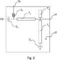
- FIG. figure 2An adaptation circuit intended to be connected to a non-linear impedance L comprising a superconductor according to a first embodiment of a first aspect of the invention is illustrated in FIG. figure 2 .
- the adaptation circuitincludes a first terminal said first connection port J1 intended to be connected to a first terminal B1 of the nonlinear impedance L, a second terminal said second connection port J2 intended to be connected to a second terminal B2 of the non-linear impedance linear L, a third terminal said input / output terminal ES for receiving the signal to be amplified, the amplification being done with a power gain G and a bandwidth BW, and a fourth terminal said TA power terminal intended to be connected to an ST bias source and configured so that a voltage V is applied between the first connection port J1 and the second connection port J2.
- the process associated with the frequency f p + f slost half of the incident signal and only the other half can be amplified which is equivalent to reducing the power gain by a factor .
- the noiseis increased by a factor of two to go from half a photon h f 2 to a photon hf.
- the band f p + f scan be greatly reduced by minimizing the impedance at the frequency f p + f s as proposed by the invention, it is possible to tend towards the optimal noise.
- part of the passive electrical elementsis realized using waveguide segments (or CPW for CoPlanar Waveguide in English). These can be made of a superconducting material to minimize losses by joule effect and therefore the thermal noise at the circuit.
- the impedance of the waveguide segmentsis therefore easy to control through their dimensions which makes their use very advantageous.
- passive electrical elementssuch as capacitors or inductors, for example when the dimensional requirements are not compatible with the use of waveguide segments.
- the adaptation circuit illustrated in FIG. figure 2comprises a first waveguide segment T 1 whose first end is connected to the power supply terminal TA via an inductance L 1 and to the input / output terminal ES via a first capacity C 1 and a second end is connected to the first connection port J1.
- this first waveguide segment T 1makes it possible to transform the impedance so as to favor a broad frequency band or an optimal noise depending on the applications envisaged.
- the circuitalso comprises a second waveguide segment T 2 , a first end of which is connected to ground via a second capacitance C 2 and a second end is connected to the first connection port J 1.
- the second capacitanceis chosen to behave in short circuit at frequencies f i , f s and f p .
- the circuitincludes a third waveguide segment T 3 , a first end of which is connected to an infinite impedance (i.e. an open circuit) and a second end of which is connected to the first connection port. J1. Finally, the second connection port J2 is connected to ground.
- This CPWthus makes it possible to produce antiresonances of the impedance between the first connection port J1 and the second connection port J2 at the frequencies k ⁇ f p with k ⁇ [1, + ⁇ ] and has a frequency close to the zero frequency , but allows to apply a DC voltage at the connection port J1.
- the real part of the impedance Re (Z (f))is zero at said frequencies.
- the real part of the impedance as a function of the frequency of this particular embodimentis illustrated in FIG. figure 3 .
- the impedanceis zero for the pump frequencies f p , plus pump signal f s + f p , idler plus pump f p + f i and the first harmonic of the pump frequency 2f p .
- the impedancehas a high impedance (and therefore not zero) at frequencies f s and f i .
- the measured impedancehas a local maximum at frequencies f s and f i .
- the structure of the figure 2therefore fulfills all the conditions mentioned above.
- the impedance Z 1 of the first waveguide T 1is chosen to be equal to 150 ⁇ .
- the real part of the impedance as a function of the frequency of this embodimentis illustrated in FIG. figure 4 . It can be noted that if the resonances appear at the same frequencies as before, the peaks associated with these resonances are higher and narrower. In other words, it is possible to modify the gain and the bandwidth of an amplifier comprising such a circuit by modifying the value of the impedance Z 1 of the first waveguide T 1 .
- the value of this impedancemakes it possible to obtain a wide bandwidth around the signal frequency f s, with however a minimum at the frequency f p + f s narrow and therefore a frequency range where the noise is optimal narrower.
- the bandwidth around the signal frequency f sis reduced but makes it possible to obtain a minimum at the frequency f p + f s which is wider and therefore a frequency range where the noise is optimal. wider.
- f s6 GHz
- f i16.8 GHz
- f p22.8 GHz
- the real part of the impedance as a function of the frequency of this particular embodimentis illustrated in FIG. figure 5 .
- the frequency of the signal to be amplified f smay be different from the frequency idler f i and advantageously lower than the latter.
- FIG. figure 6To optimize both the bandwidth BW at the signal frequency f s and the width of the frequency range where the noise is optimal, a second embodiment of a first aspect of the invention is illustrated in FIG. figure 6 .
- the matching circuitcomprises a first waveguide segment T 1 whose first end is connected to the terminal at the input / output terminal ES and a second end is connected to a first end of the waveguide.
- the second ends of the second waveguide T ' 2 and third waveguide T' 3are each connected to an infinite impedance (that is to say an open circuit).
- the second waveguide segment T ' 2is further capacitively coupled to a fourth waveguide T " 2 and the third waveguide segment T' 3 is further capacitively coupled to a fifth waveguide. T waveguide 3 so as to form a coupler.
- a first end of the fourth waveguide T " 2is connected to ground via a capacitor C 2 and to the power supply terminal TA.
- a second end of the fourth waveguide T" 2is connected to the first connection port J1.
- a first end of the fifth waveguide T " 3is connected to an infinite impedance (i.e. an open circuit)
- a second end of the fifth waveguide T" 3is connected to the first connection port J1.
- the second connection port J2is connected to the mass.
- the first waveguide segment T 1makes it possible to transform the impedance so as to favor a broad frequency band without compromising on the optimal noise.
- the amplitude of the real part of the impedance as a function of the frequency obtained with this embodimentis illustrated in FIG. figure 7 .
- the impedancehas a high impedance (thus non-zero) at frequencies f s and f i . More particularly, the impedance has a high impedance plateau wide of several GHz around the signal frequencies f s and idler f i . In other words, an amplifier comprising such a circuit will present a wide frequency band around the frequency signal f s wherein the signal will be amplified.
- the impedanceis substantially equal to zero for the frequencies f p and f p + f s as well as at low frequencies.
- the impedance obtained with this structurethus fulfills the previously established criteria of a noise of less than 1 photon and also makes it possible to separate the DC portion of the circuit of the AC portion.
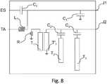
- FIG. figure 8A third embodiment of an adaptation circuit according to a first aspect of the invention is illustrated in FIG. figure 8 .
- the first connection port J1is connected to the input / output terminal ES via a fourth capacitor C 4 .
- the first connection port J1is also connected to ground via a first capacitor C 1 and to the supply terminal TA via an inductor L 1 .
- the circuitalso includes a first waveguide segment T 1 whose first end is connected to an infinite impedance (i.e., an open circuit) and a second end of which is connected to ground via
- the circuitalso includes a second waveguide segment T 2 , a first end of which has an infinite impedance (i.e. an open circuit) and a second end of which is connected to the second end.
- the circuitfurther includes a third waveguide segment T 3 , one end of which is connected to an infinite impedance (i.e., an open circuit) and a second end of which is connected to the second connection port J2. via a third capacitor C 3 .
- the circuitalso comprises a fourth waveguide segment T ' 1 whose first end is connected to ground and a second end of which is connected to the second connection port J2.
- the first waveguide segment T 1is capacitively coupled to the fourth waveguide T ' 1 .
- the second capacitance C 2has an impedance of 1 fF.
- the third capacitor C 3has an impedance of 0.5 fF.
- the first capacitor C 1has an impedance of 100 fF
- the fourth capacitor C 4has an impedance of 100 pF
- the inductance L 1has an impedance of 100nH
- the resistor Rhas an impedance of 5 ⁇ .
- the fourth capacitance C 4 and the inductance L 1make it possible to control the low cut-off frequency (approximately 80 MHz). It is also possible to choose impedance values for these elements a hundred times smaller to center the bandwidth around 10 GHz.
- the amplitude of the real part of the impedance as a function of the frequency obtained with this embodimentis illustrated in FIG. figure 9 .
- the three preceding embodimentsdemonstrate through four examples how to obtain a matching circuit having the characteristics necessary for obtaining a low noise amplifier. It is therefore possible, from an adaptation circuit according to a first aspect of the invention, to provide a low noise amplifier. Such an amplifier is illustrated in figure 10 .
- This amplifierhas a non-linear impedance in the form of a Josephson J junction.
- the superconducting material of the junctionis chosen so that f s ⁇ 2 ⁇ h with ⁇ the superconducting gap of the superconducting material.
- the amplifieralso has a bias source, here in the form of a voltage source ST.
- the latteris connected via the T-connection so as to apply a voltage V across the Josephson junction. The presence of this T-connection ensures that the high-frequency signals originate or are sent to the terminal. ES input / output port while the low frequency signals are coming from or being sent to the TA power terminal.
- the materialcan be chosen from all superconductors such as aluminum.
- the nonlinear impedanceis constituted by a Josephson junction.
- the use of a Josephson junctionprovides an advantage in terms of manufacturing, such a junction being easy to obtain.
- the gainis directly dependent on the critical current. In other words, when using a Josephson junction as a non-linear impedance, the gain of amplification can vary from one amplifier to another.
- a SQUID(English Superconducting Quantum Interference Device).
- a SQUIDis in the form of a superconducting loop comprising two Josephson junctions.
- the critical current of such a structurecan be modulated by varying the magnetic flux passing through the loop by means of a magnetic field. It is therefore possible to adjust in situ the critical current of the SQUID and thus the gain of the amplifier using such a SQUID.
- a magnetic fieldmay be applied by means of a power line close to the SQUID and in which a current flows.
Landscapes
- Engineering & Computer Science (AREA)
- Power Engineering (AREA)
- Amplifiers (AREA)
- Microwave Amplifiers (AREA)
Abstract
Translated fromFrenchDescription
Translated fromFrenchLe domaine technique de l'invention est celui des amplificateurs hautes fréquences. La présente invention concerne un circuit d'adaptation pour un amplificateur bas bruit. L'invention concerne également un amplificateur bas bruit comprenant un tel circuit d'adaptation et en particulier un amplificateur bas bruit à jonction Josephson.The technical field of the invention is that of high frequency amplifiers. The present invention relates to an adaptation circuit for a low noise amplifier. The invention also relates to a low-noise amplifier comprising such a matching circuit and in particular a low-noise Josephson junction amplifier.
Dans le cadre de la recherche fondamentale ou de la radioastronomie, il est souvent nécessaire d'avoir recours à des amplificateurs dit très faible bruit, c'est-à-dire des amplificateurs dont le bruit est aussi proche que possible de la limite théorique imposée par la mécanique quantique, et ce, pour des fréquences allant du MHz au THz. Il est possible de distinguer deux types d'amplificateurs : les amplificateurs préservant la phase et les amplificateurs sensibles à la phase. Les amplificateurs sensibles à la phase ne sont pas soumis à la limitation théorique mais ils sont difficiles à utiliser car la phase du signal à amplifier doit parfaitement correspondre à la quadrature amplifiée. Les amplificateurs préservant la phase sont soumis à la limite quantique mais n'imposent en revanche aucune condition quant à la phase du signal à amplifier.In the context of basic research or radio astronomy, it is often necessary to use so-called very low-noise amplifiers, ie amplifiers whose noise is as close as possible to the theoretical limit imposed. by quantum mechanics for frequencies from MHz to THz. Two types of amplifiers can be distinguished: phase-preserving amplifiers and phase-sensitive amplifiers. Phase-sensitive amplifiers are not subject to theoretical limitation but they are difficult to use because the phase of the signal to be amplified must perfectly correspond to the amplified quadrature. Phase-preserving amplifiers are subject to the quantum limit but do not impose any condition on the phase of the signal to be amplified.
Dans le domaine de l'amplification haute fréquence et très haute fréquence il est connu d'utiliser une amplification par réflexion. Cette dernière est obtenue par exemple à l'aide d'une ligne de transmission d'impédance Z0 terminée par une impédance ZL(f) où f est la fréquence du signal. Le coefficient de réflexion en tension d'une telle structure est donnée par
Dans le domaine de l'amplification, il est aussi connu d'utiliser des transistors semiconducteurs travaillant à des températures cryogéniques. Les transistors sont polarisés en tension ce qui rend l'utilisation de ce type d'amplificateurs très facile à mettre en oeuvre. En revanche leur niveau de bruit, même à température cryogénique, reste encore élevé : de l'ordre de 10 photons dans le meilleur des cas, soit 20 fois la limite quantique. Pour limiter le bruit au maximum, il a été proposé d'utiliser un amplificateur paramétrique dans lequel l'impédance négative est obtenue par exemple par l'intermédiaire de quatre jonctions Josephson. Le circuit de l'amplificateur possède un premier mode à la fréquence signal fs et un deuxième mode à la fréquence idler fi. Les paramètres du circuit sont modifiés à l'aide de la pompe de fréquence fp. Cet amplificateur permet d'obtenir une bande passante de quelques MHz avec un bruit proche de la limite quantique mais nécessite la génération d'une pompe, ce qui le rend complexe à mettre en oeuvre.In the field of amplification, it is also known to use semiconductor transistors operating at cryogenic temperatures. The transistors are biased in voltage which makes the use of this type of amplifiers very easy to implement. On the other hand, their noise level, even at cryogenic temperature, remains high: in the order of 10 photons in the best case, ie 20 times the quantum limit. To limit the noise to the maximum, it has been proposed to use a parametric amplifier in which the negative impedance is obtained for example via four Josephson junctions. The circuit of the amplifier has a first mode at the signal frequency fs and a second mode at the frequency idler fi . The circuit parameters are modified using the frequency pump fp . This amplifier makes it possible to obtain a bandwidth of a few MHz with a noise close to the quantum limit but requires the generation of a pump, which makes it complex to implement.
Une autre manière de comprendre cette amplification paramétrique est d'envisager cette dernière en termes de photons, chaque photon étant associé à une énergie. Par exemple, un premier photon d'énergie E1 peut être converti en un deuxième photon d'énergie E2 et un troisième photon d'énergie E3 si la relation entre ces trois énergies est telle que E1 = E2 + E3 (il s'agit d'une condition nécessaire mais pas suffisante). Sachant qu'il est possible d'associer à chaque énergie une fréquence, cette égalité devient f1 = f2 + f3. Si l'on cherche à amplifier un signal de fréquence f2, il est donc possible d'avoir recours à un signal de fréquence f1 sous réserve qu'un mode, c'est-à-dire une résonnance du système, à une fréquence f3 soit également présent. Dans la suite, la fréquence f1 est appelée fréquence pompe fp, la fréquence f2 est appelée fréquence signal fs et la fréquence f3 est appelée fréquence idler fi. Il est possible d'obtenir une amplification d'un signal de fréquence fs par la génération d'autres photons de signal de fréquence fs à partir des photons de pompe de fréquence fp, cette génération entrainant également la génération de photons idler de fréquence fi. Afin que ce processus d'amplification ait lieu, il est en outre nécessaire, en plus de la condition de conservation de l'énergie, que les différentes fréquences soient couplées entre elles. Un tel couplage est réalisé à l'aide d'une impédance non linéaire.Another way to understand this parametric amplification is to consider the latter in terms of photons, each photon being associated with an energy. For example, a first energy photon E1 can be converted into a second energy photon E2 and a third energy photon E3 if the relationship between these three energies is such that E1 = E2 + E3 (This is a necessary but not sufficient condition). Knowing that it is possible to associate with each energy a frequency, this equality becomes f1 = f2 + f3 . If it is desired to amplify a signal of frequency f2 , it is therefore possible to use a signal of frequency f1 provided that a mode, ie a resonance of the system, at a frequency of frequency f3 is also present. In the following, the frequency f1 is called the pump frequency fp , the frequency f2 is called the signal frequency fs and the frequency f3 is called the frequency idler fi . It is possible to obtain an amplification of a signal of frequency fs by the generation of other photons of frequency signal fs from the pump photons of frequency fp , this generation also causing the generation of photons idler of frequency fi . So that this process of amplification takes place, it is also necessary, in addition to the condition of energy conservation, that the different frequencies are coupled together. Such coupling is achieved using a non-linear impedance.
Alternativement, il a été proposé d'utiliser un amplificateur dans lequel l'impédance négative est obtenue à l'aide d'une jonction Josephson polarisée en tension. Cette polarisation en tension permet de s'affranchir de la pompe et contribue à la simplification du dispositif. En effet, une fois la jonction polarisée, les paires de Cooper responsables du courant supraconducteur dotées d'une énergie proportionnelle à la tension appliquée à la jonction vont devoir relaxer, c'est-à-dire revenir à leur état énergétique fondamental. Or, le seul mécanisme permettant cette relaxation conduit à l'émission d'un ou plusieurs photons dont l'énergie est liée à la tension de polarisation appliquée. Autrement dit, la tension appliquée permet de générer des photons de la même manière que la fréquence pompe de l'amplificateur paramétrique, la fréquence de ces photons étant ici fonction de la tension appliquée à la jonction.Alternatively, it has been proposed to use an amplifier in which the negative impedance is obtained using a voltage-biased Josephson junction. This voltage bias eliminates the pump and contributes to the simplification of the device. In fact, once the junction is polarized, the Cooper pairs responsible for the superconducting current provided with an energy proportional to the voltage applied to the junction will have to relax, that is to say return to their fundamental energetic state. However, the only mechanism allowing this relaxation leads to the emission of one or more photons whose energy is related to the applied bias voltage. In other words, the applied voltage makes it possible to generate photons in the same manner as the pump frequency of the parametric amplifier, the frequency of these photons being here a function of the voltage applied to the junction.
De plus, l'amplification peut être obtenue, dans le mode de réalisation le plus simple, avec une seule jonction Josephson. Un tel dispositif est illustré à la
Dans ce dispositif, il est possible de distinguer deux situations. Pour les hautes et basses fréquences, la jonction Josephson est court-circuitée par le circuit d'adaptation. La partie réelle du coefficient de réflexion est alors égale à Re(G(f)) =
Il existe donc un besoin de fabriquer un amplificateur permettant de maintenir le niveau de bruit similaire à celui d'un amplificateur paramétrique tout en présentant la simplicité d'un amplificateur à jonction Josephson polarisée en tension.There is therefore a need to manufacture an amplifier to maintain the noise level similar to that of a parametric amplifier while having the simplicity of a voltage-biased Josephson junction amplifier.
L'invention offre une solution aux problèmes évoqués précédemment en proposant un circuit d'adaptation permettant de diminuer le bruit généré par un amplificateur à jonction Josephson polarisée en tension. Elle propose également un amplificateur utilisant un tel circuit.The invention offers a solution to the problems mentioned above by proposing an adaptation circuit making it possible to reduce the noise generated by a voltage-polarized Josephson junction amplifier. It also offers an amplifier using such a circuit.
Un premier aspect de l'invention concerne un circuit d'adaptation d'impédance destiné à être connecté à une impédance non-linéaire comprenant un supraconducteur, ledit circuit comportant un premier terminal dit premier port de connexion destiné à être connecté à une première borne de l'impédance non-linéaire, un deuxième terminal dit deuxième port de connexion destiné à être connecté à une deuxième borne de l'impédance non-linéaire, un troisième terminal dit terminal d'entrée/sortie destiné à recevoir le signal à amplifier avec un gain en puissance G et une bande passante BW et un quatrième terminal dit terminal d'alimentation destiné à être connecté à une source de polarisation et configuré pour qu'une tension V puissent être appliquée entre le premier port de connexion et le deuxième port de connexion.A first aspect of the invention relates to an impedance matching circuit intended to be connected to a non-linear impedance comprising a superconductor, said circuit comprising a first terminal said first connection port intended to be connected to a first terminal of the non-linear impedance, a second terminal said second connection port intended to be connected to a second terminal of the nonlinear impedance, a third terminal called input / output terminal for receiving the signal to be amplified with a power gain G and a bandwidth BW and a fourth terminal said power terminal to be connected to a bias source and configured so that a voltage V can be applied between the first connection port and the second connection port.
Le circuit d'adaptation selon l'invention comporte une pluralité de composants électriques passifs configurés de sorte que l'impédance Z(f) entre le premier port de connexion et le deuxième port de connexion pour un signal de fréquence f a une partie réelle Re(Z(f)) telle que :
- Re(Z(fs)) > 0 avec fs une première fréquence dite fréquence signal ;
- Re(Z(fi)) > 0 avec fi une deuxième fréquence dite fréquence idler ;


- Re (Z (fs ))> 0 with fs a first frequency called the signal frequency;
- Re (Z (fi ))> 0 with fi a second frequency called idler frequency;
On entend par Z(fx) la valeur de l'impédance pour une fréquence appartenant à une plage de fréquences de largeur définie et centrée sur la fréquence fx. Sauf précision contraire, lorsqu'il est fait mention d'une fréquence fx cette dernière doit être comprise comme une fréquence f appartenant à un intervalle [fx - Δf,fx + Δf] avec Δf < 0.5fs voire Δf < 0.1fs. La source de polarisation peut notamment être choisie parmi une source de tension, une source de courant ou bien encore une impédance finie.Z (fx ) is the value of the impedance for a frequency belonging to a frequency range of defined width and centered on the frequency fx . Unless otherwise specified, when reference is made to a frequency fx, the latter must be understood as a frequency f belonging to an interval [fx - Δf, fx + Δf] with Δf <0.5fs or even Δf <0.1 fs . The polarization source may in particular be chosen from a voltage source, a current source or even a finite impedance.
De manière générale, la probabilité qu'a une paire de Cooper de relaxer en générant un photon à la fréquence f, est approximativement proportionnelle à l'impédance vue par l'élément supraconducteur à ladite fréquence f. En particulier, une paire de Cooper a une plus grande probabilité de relaxer en émettant un photon à la fréquence f lorsqu'un mode de résonnance de l'impédance Z(f) vu par l'impédance non linéaire est présent à cette fréquence. Les inventeurs, tirant parti de cette propriété, ont identifié les conditions concernant cette impédance qui limitent le bruit généré.In general, the probability that a Cooper pair will relax by generating a photon at the frequency f, is approximately proportional to the impedance seen by the superconducting element at said frequency f. In particular, a pair of Cooper has a greater probability of relaxing by emitting a photon at the frequency f when a resonance mode of the impedance Z (f) seen by the nonlinear impedance is present at this frequency. The inventors, taking advantage of this property, have identified the conditions concerning this impedance which limit the noise generated.
Les conditions Re(Z(fs)) > 0 et Re(Z(fi)) > 0 permettent de s'assurer de l'amplification du signal à la fréquence de signal fs. En effet l'impédance étant non nulle à ces fréquences, des photons peuvent être générés auxdites fréquences.The conditions Re (Z (fs ))> 0 and Re (Z (fi ))> 0 make it possible to ensure the amplification of the signal at the signal frequency fs . Indeed the impedance being non-zero at these frequencies, photons can be generated at said frequencies.
La condition
De plus, la condition
En outre, la condition
Enfin, la condition nfp = fs + fi permet de s'assurer que la condition concernant la conservation de l'énergie évoquée précédemment est remplie.Finally, the condition nfp = fs + fi makes it possible to ensure that the condition relating to the conservation of the energy mentioned above is fulfilled.
Autrement dit, grâce au circuit d'adaptation selon l'invention, le bruit inutile n'est pas ramené depuis les fréquences élevées vers la fréquence d'amplification. De plus, le signal utile n'est pas perdu vers d'autres fréquences.In other words, thanks to the matching circuit according to the invention, the unnecessary noise is not brought back from the high frequencies to the amplification frequency. In addition, the useful signal is not lost to other frequencies.
Outre les caractéristiques qui viennent d'être évoquées dans le paragraphe précédent, le circuit d'adaptation d'impédance selon un premier aspect de l'invention peut présenter une ou plusieurs caractéristiques complémentaires parmi les suivantes, considérées individuellement ou selon toutes les combinaisons techniquement possibles.In addition to the characteristics that have just been mentioned in the preceding paragraph, the impedance matching circuit according to a first aspect of the invention may have one or more additional characteristics among the following, considered individually or in any technically possible combination. .
Avantageusement,
Avantageusement,
Avantageusement,
Avantageusement, le terminal d'entrée/sortie est destiné à être connecté à une impédance de valeur Z0 et

Avantageusement,

Avantageusement,
Avantageusement, n = 1 ou, autrement dit,
Avantageusement,
Avantageusement, l'impédance Z(f) présente un maximum local en fs et/ou fi. Ainsi, le circuit d'adaptation présente des modes de résonnance à la fréquence signal fs et/ou à la fréquence idler fi ce qui permet de garantir qu'à ces fréquences un photon a une forte probabilité d'être généré lors de la relaxation des paires de Cooper.Advantageously, the impedance Z (f) has a local maximum in fs and / or fi . Thus, the matching circuit has resonant modes to the frequency signal fs and / or the idler frequency fi which ensures that at these frequencies a photon has a high probability of being generated during the Cooper pairs relaxation.
Avantageusement,
Avantageusement, l'impédance Z(f) présente un minimum local en fp et/ou fp + fi et/ou fp + fs. Ainsi, le circuit présente des anti-résonnances à la fréquence pompe fp, à la fréquence pompe plus la fréquence idler fp + fi et à la fréquence pompe plus la fréquence signal fp + fs ce qui permet de garantir qu'à ces fréquences un photon a une faible probabilité d'être généré lors de la relaxation des paires de Cooper.Advantageously, the impedance Z (f) has a local minimum in fp and / or fp + fi and / or fp + fs . Thus, the circuit has anti-resonances at the pump frequency fp , at the pump frequency plus the frequency idler fp + fi and at the pump frequency plus the signal frequency fp + fs , which makes it possible to guarantee that at these frequencies a photon has a low probability of being generated during the relaxation of the Cooper pairs.
Avantageusement, la pluralité de composants électriques passifs comporte :
- un premier segment de guide d'onde dont une première extrémité est connectée au terminal d'alimentation par l'intermédiaire d'une inductance et au terminal d'entrée/sortie par l'intermédiaire d'une première capacité et une deuxième extrémité est connectée au premier port de connexion ;
- un deuxième segment de guide d'onde dont une première extrémité est connectée à la masse par l'intermédiaire d'une deuxième capacité et une deuxième extrémité est connectée au premier port de connexion ;
- un troisième segment de guide d'onde dont une première extrémité est connectée à une impédance infinie et une deuxième extrémité est connectée au premier port de connexion ;
- a first waveguide segment whose first end is connected to the power supply terminal via an inductor and at the input / output terminal via a first capacitance and a second end is connected to the first connection port;
- a second waveguide segment having a first end connected to the ground via a second capacitor and a second end connected to the first connection port;
- a third waveguide segment having a first end connected to an infinite impedance and a second end connected to the first connection port;
En outre, le deuxième port de connexion est connecté à la masse. Ainsi, les propriétés électriques sont obtenues à l'aide de guides d'onde. L'impédance et la fréquence de résonance de ces derniers étant facile à contrôler par l'intermédiaire de leurs dimensions, leur utilisation est très avantageuse.In addition, the second connection port is connected to ground. Thus, the electrical properties are obtained using waveguides. The impedance and resonance frequency of the latter being easy to control through their dimensions, their use is very advantageous.
Avantageusement, la pluralité de composants électriques passifs comporte :
- un premier segment de guide d'onde dont une première extrémité est connectée au terminal d'entrée/sortie ;
- un deuxième segment de guide d'onde dont une première extrémité est connectée à une deuxième extrémité du premier segment de guide d'onde et dont une deuxième extrémité est connectée à une impédance infinie ;
- un troisième segment de guide d'onde dont une première extrémité est connectée à la deuxième extrémité du premier segment de guide d'onde et dont une deuxième extrémité est connectée à une impédance infinie ;
- un quatrième segment de guide d'onde dont une première extrémité est connectée à la masse par l'intermédiaire d'une capacité et au terminal d'alimentation et dont une deuxième extrémité est connectée au premier port de connexion ;
- un cinquième segment de guide d'onde dont une première extrémité est connectée à une impédance infinie et dont une deuxième extrémité est connecté au premier port de connexion.
- a first waveguide segment having a first end connected to the input / output terminal;
- a second waveguide segment having a first end connected to a second end of the first waveguide segment and having a second end connected to an infinite impedance;
- a third waveguide segment having a first end connected to the second end of the first waveguide segment and having a second end connected to an infinite impedance;
- a fourth waveguide segment whose first end is connected to ground via a capacitor and to the power supply terminal and a second end of which is connected to the first connection port;
- a fifth waveguide segment whose first end is connected to an infinite impedance and whose second end is connected to the first connection port.
En outre, le deuxième port de connexion est connecté à la masse, le deuxième segment de guide d'onde est en outre couplé de manière capacitive au quatrième segment de guide d'onde et le troisième segment de guide d'onde est couplé de manière capacitive au cinquième segment de guide d'onde de sorte à former un coupleur.In addition, the second connection port is grounded, the second waveguide segment is further capacitively coupled to the fourth waveguide segment, and the third waveguide segment is coupled to the second waveguide segment. capacitively way to the fifth waveguide segment so as to form a coupler.
Avantageusement, la pluralité de composants électriques passifs comporte :
- une inductance L1 dont une première borne est connectée au terminal d'alimentation et dont une deuxième borne est connectée à la masse par l'intermédiaire d'une première capacité, au terminal d'entrée/sortie par l'intermédiaire d'une quatrième capacité et au premier port de connexion ;
- un premier segment de guide d'onde dont une première extrémité est connectée à une impédance infinie et dont une deuxième extrémité est connectée à la masse par l'intermédiaire d'une résistance ;
- un deuxième segment de guide d'onde dont une première extrémité est à une impédance infinie et dont une deuxième extrémité est connectée au deuxième port de connexion par l'intermédiaire d'une deuxième capacité ;
- un troisième segment de guide d'onde dont une extrémité est connectée à une impédance infinie et dont une deuxième extrémité est connectée au deuxième port de connexion par l'intermédiaire d'une troisième capacité ;
- un quatrième segment de guide d'onde dont une première extrémité est connectée à la masse et dont une deuxième extrémité est connectée au deuxième port de connexion.
- an inductance L1 , a first terminal of which is connected to the supply terminal and a second terminal of which is connected to ground via a first capacitor, to the input / output terminal via a fourth terminal; capacity and the first connection port;
- a first waveguide segment whose first end is connected to an infinite impedance and whose second end is connected to ground via a resistor;
- a second waveguide segment whose first end is at infinite impedance and a second end of which is connected to the second connection port through a second capacitance;
- a third waveguide segment whose one end is connected to an infinite impedance and a second end of which is connected to the second connection port through a third capacitance;
- a fourth waveguide segment having a first end connected to the ground and a second end connected to the second connection port.
En outre, le premier segment de guide d'onde est couplé de manière capacitive au quatrième guide d'onde.In addition, the first waveguide segment is capacitively coupled to the fourth waveguide.
Avantageusement, au moins un segment de guide d'onde est réalisé dans un matériau supraconducteur afin de diminuer la dissipation, et donc le bruit thermique, au sein du circuit d'adaptation.Advantageously, at least one waveguide segment is made of a superconductive material in order to reduce the dissipation, and therefore the thermal noise, within the adaptation circuit.
Un deuxième aspect de l'invention concerne un amplificateur à réflexion comportant un circuit d'adaptation d'impédance selon un premier aspect de l'invention, une source de polarisation connectée au terminal d'alimentation, une impédance non linéaire comprenant un supraconducteur, ladite impédance non-linéaire comportant une premier borne et une deuxième borne, la première borne de l'impédance étant connectée au premier port de connexion du circuit d'adaptation, la deuxième borne de l'impédance étant connectée au deuxième port de connexion du circuit d'adaptation. De plus, la tension V appliquée entre le premier terminal de connexion et le deuxième terminal de connexion au moyen de la source de polarisation est choisie de sorte que
Avantageusement, dans l'amplificateur selon un deuxième aspect de l'invention, le matériau supraconducteur de l'impédance non-linéaire est choisi de sorte que


Avantageusement,
En outre, ce deuxième aspect de l'invention permet d'obtenir des performances proches ou équivalentes à celle d'un amplificateur paramétrique, mais avec une alimentation DC au lieu d'une alimentation par un signal micro-ondes. Cela rend l'utilisation d'un tel amplificateur bien plus simple et moins onéreuse, surtout dans un environnement cryogénique. Un tel avantage devient notamment important au-dessus de 10 GHz.In addition, this second aspect of the invention makes it possible to obtain performances close to or equivalent to that of a parametric amplifier, but with a DC supply instead of a supply by a microwave signal. This makes the use of such an amplifier much simpler and less expensive, especially in a cryogenic environment. Such an advantage becomes particularly important above 10 GHz.
De plus, le fait de travailler avec une jonction polarisée en tension permet de travailler à plus haute fréquence. En effet, dans le cas d'un amplificateur paramétrique, la jonction est dans l'état supraconducteur où elle a un comportement inductif. Cette inductance, ensemble avec la capacité de la jonction, détermine la fréquence plasma de la jonction a une valeur environ égale à

Par ailleurs, comme cela a été présenté précédemment, il est préférable d'avoir une fréquence idler fi telle que
Enfin, le gain de l'amplificateur selon l'invention augmente avec le courant critique de la jonction (ou du SQUID), tandis que dans le cas des amplificateurs paramétriques il diminue. Ceci peut faciliter l'optimisation de l'amplificateur pour avoir à la fois un fort gain pour une large bande passante et une large étendue dynamique (point de compression élevé) qui nécessite des courants critiques élevés.Finally, the gain of the amplifier according to the invention increases with the critical current of the junction (or SQUID), while in the case of parametric amplifiers it decreases. This can facilitate the optimization of the amplifier to have both a high gain for a wide bandwidth and a large dynamic range (high compression point) that requires high critical currents.
Outre les caractéristiques qui viennent d'être évoquées dans le paragraphe précédent, l'amplificateur à réflexion selon un deuxième aspect de l'invention peut présenter une ou plusieurs caractéristiques complémentaires parmi les suivantes, considérées individuellement ou selon toutes les combinaisons techniquement possibles.In addition to the characteristics that have just been mentioned in the preceding paragraph, the reflection amplifier according to a second aspect of the invention may have one or more additional characteristics among the following, considered individually or in any technically possible combination.
Avantageusement, l'impédance non-linéaire comprend une jonction Josephson. La jonction Josephson présente notamment l'avantage d'être un élément non linéaire avec des caractéristiques physiques et un comportement bien compris donc plus facile à mettre en oeuvre.Advantageously, the nonlinear impedance comprises a Josephson junction. The Josephson junction has the advantage of being a non-linear element with physical characteristics and behavior well understood and easier to implement.
Avantageusement, la jonction Josephson est de type SIS (Supraconducteur/Isolant/Supraconducteur). Une jonction de type SIS présente l'avantage d'être un élément non linéaire non dissipatif ce qui évite de créer des processus de conversion parasites.Advantageously, the Josephson junction is of SIS type (superconductor / insulator / superconductor). A SIS type junction has the advantage of being a non-dissipative non-linear element, which avoids creating spurious conversion processes.
Avantageusement, l'impédance non-linéaire supraconductrice comprend un SQUID. Ainsi, il est possible de moduler le gain de l'amplificateur à l'aide d'un champ magnétique.Advantageously, the superconducting non-linear impedance comprises a SQUID. Thus, it is possible to modulate the gain of the amplifier using a magnetic field.
Avantageusement, la bande passant BW de l'amplificateur est choisie de sorte que
L'invention et ses différentes applications seront mieux comprises à la lecture de la description qui suit et à l'examen des figures qui l'accompagnent.The invention and its various applications will be better understood by reading the following description and examining the figures that accompany it.
Les figures sont présentées à titre indicatif et nullement limitatif de l'invention.
- La
figure 1 montre un amplificateur à jonction Josephson selon l'état de l'art antérieur. - La
figure 2 montre un circuit d'adaptation selon un premier mode de réalisation d'un premier aspect de l'invention. - La
figure 3 montre un graphique présentant la partie réelle de l'impédance en fonction de la fréquence d'un circuit d'adaptation selon un premier mode de réalisation d'un premier aspect de l'invention. - La
figure 4 montre un graphique présentant la partie réelle de l'impédance en fonction de la fréquence d'un circuit d'adaptation selon une première variante d'un premier mode de réalisation d'un premier aspect de l'invention. - La
figure 5 montre un graphique présentant la partie réelle de l'impédance en fonction de la fréquence d'un circuit d'adaptation selon une deuxième variante d'un premier mode de réalisation d'un premier aspect de l'invention. - La
figure 6 montre un circuit d'adaptation selon un deuxième mode de réalisation d'un premier aspect de l'invention. - La
figure 7 montre un graphique présentant la partie réelle de l'impédance en fonction de la fréquence d'un circuit d'adaptation selon un deuxième mode de réalisation d'un premier aspect de l'invention. - La
figure 8 montre un circuit d'adaptation selon un troisième mode de réalisation d'un premier aspect de l'invention. - La
figure 9 montre un graphique présentant la partie réelle de l'impédance en fonction de la fréquence d'un circuit d'adaptation selon un troisième mode de réalisation d'un premier aspect de l'invention. - La
figure 10 montre un amplificateur à jonction Josephson selon un mode de réalisation d'un deuxième aspect de l'invention.
- The
figure 1 shows a Josephson junction amplifier according to the state of the prior art. - The
figure 2 shows an adaptation circuit according to a first embodiment of a first aspect of the invention. - The
figure 3 shows a graph showing the real part of the impedance as a function of the frequency of an adaptation circuit according to a first embodiment of a first aspect of the invention. - The
figure 4 shows a graph showing the real part of the impedance as a function of the frequency of an adaptation circuit according to a first variant of a first embodiment of a first aspect of the invention. - The
figure 5 shows a graph showing the real part of the impedance as a function of the frequency of an adaptation circuit according to a second variant of a first embodiment of a first aspect of the invention. - The
figure 6 shows an adaptation circuit according to a second embodiment of a first aspect of the invention. - The
figure 7 shows a graph showing the real part of the impedance as a function of the frequency of an adaptation circuit according to a second embodiment of a first aspect of the invention. - The
figure 8 shows an adaptation circuit according to a third embodiment of a first aspect of the invention. - The
figure 9 shows a graph showing the real part of the impedance as a function of the frequency of an adaptation circuit according to a third embodiment of a first aspect of the invention. - The
figure 10 shows a Josephson junction amplifier according to an embodiment of a second aspect of the invention.
Sauf précision contraire, un même élément apparaissant sur des figures différentes présente une référence unique. Tous les modes de réalisation suivants ont été conçus dans le cas où le terminal d'entrée/sortie ES est destiné à être connecté ou est connecté à une ligne d'impédance Z0 égale à 50 Ω.Unless otherwise specified, the same element appearing in different figures has a unique reference. All the following embodiments have been designed in the case where the input / output terminal ES is intended to be connected or is connected to an impedance line Z0 equal to 50 Ω.
Un circuit d'adaptation destiné à être connecté à une impédance non-linéaire L comprenant un supraconducteur selon un premier mode de réalisation d'un premier aspect de l'invention est illustré à la
Le circuit d'adaptation comporte également une pluralité de composants électriques passifs (T1, T2, T3, C1, C2, L1) configurés de sorte que l'impédance Z(f) entre le premier port de connexion J1 et le deuxième port de connexion J2 pour un signal de fréquence f a une partie réelle Re(Z(f)) telle que :
- Re(Z(fs)) > 0 avec fs une première fréquence dite fréquence signal ;
- Re(Z(fi)) > 0 avec fi une deuxième fréquence dite fréquence idler ;


- Re (Z (fs ))> 0 with fs a first frequency called the signal frequency;
- Re (Z (fi ))> 0 with fi a second frequency called idler frequency;
En outre, la fréquence pompe est choisie de sorte que nfp = fs + fi avec n un entier appartenant à [1, +∞] et la fréquence idler est choisie de sorte que
- la bande fp - fs est due à un processus où chaque paire de Cooper qui tunnel à travers la jonction donne un photon à la fréquence fs et un photon à la fréquence fp - fs ce qui amplifie le signal à la fréquence fs (effet d'émission stimulée) et donne lieu à un bruit ajouté d'un demi-photon hfs (effet d'émission spontanée) ;
- la bande fp + fs est due à un processus où chaque paire de Cooper est décalée en fréquence de la fréquence fs à la fréquence fp + fs en absorbant l'énergie d'une paire de Cooper qui tunnel ce qui conduit à l'absorption du signal à la fréquence fs sans ajouter de bruit.
- the band fp - fs is due to a process where each Cooper pair which tunnel through the junction gives a photon at the frequency fs and a photon at the frequency fp - fs which amplifies the signal at the frequency fs (stimulated emission effect) and gives rise to an added noise of half a photon hfs (effect spontaneous emission);
- the band fp + fs is due to a process where each pair of Cooper is shifted in frequency from the frequency fs to the frequency fp + fs by absorbing the energy of a pair of Cooper which tunnel which leads at the absorption of the signal at the frequency fs without adding noise.
Si les deux processus ont la même intensité, le processus associé à la fréquence fp + fs fait perdre la moitié du signal incident et seulement l'autre moitié peut être amplifiée ce qui équivaut à réduire le gain en puissance d'un facteur deux. De plus, le bruit se trouve augmenté d'un facteur deux pour passer d'un demi-photon
Dans le mode de réalisation illustré à la
Plus particulièrement, le circuit d'adaptation illustré à la
Le circuit comporte également un deuxième segment de guide d'onde T2 dont une première extrémité est connectée à la masse par l'intermédiaire d'une deuxième capacitance C2 et une deuxième extrémité est connectée au premier port de connexion J1. La deuxième capacité est choisie de sorte à se comporter en court-circuit aux fréquences fi, fs et fp.The circuit also comprises a second waveguide segment T2 , a first end of which is connected to ground via a second capacitance C2 and a second end is connected to the first
De plus, le circuit comporte un troisième segment de guide d'onde T3 dont une première extrémité est connectée à une impédance infinie (c'est-à-dire un circuit ouvert) et dont une deuxième extrémité est connectée au premier port de connexion J1. Enfin, le deuxième port de connexion J2 est connecté à la masse.In addition, the circuit includes a third waveguide segment T3 , a first end of which is connected to an infinite impedance (i.e. an open circuit) and a second end of which is connected to the first connection port. J1. Finally, the second connection port J2 is connected to ground.
Dans un premier exemple de réalisation, on choisit fp = 12GHz et fs = fi = 6GHz. Le premier segment de guide d'onde T1 a une longueur


La partie réelle de l'impédance en fonction de la fréquence de ce mode particulier de réalisation est illustrée à la
Dans une variante de ce premier exemple de réalisation, l'impédance Z1 du premier guide d'onde T1 est choisie égale à 150 Ω. La partie réelle de l'impédance en fonction de la fréquence de cet exemple de réalisation est illustrée à la
Dans un troisième exemple de réalisation, on choisit fs = 6GHz, fi = 16.8GHz et fp = 22.8GHz. Dans ce troisième exemple de réalisation, le premier segment de guide d'onde T1 a une longueur


Pour optimiser à la fois la bande passante BW à la fréquence signal fs et la largeur de la plage de fréquences où le bruit est optimal, un deuxième mode de réalisation d'un premier aspect de l'invention est illustré à la
Dans ce mode de réalisation, le circuit d'adaptation comporte un premier segment de guide d'onde T1 dont une première extrémité est connectée au terminal au terminal d'entrée/sortie ES et une deuxième extrémité est connectée à une première extrémité d'un deuxième guide d'onde T'2 et à une première extrémité d'un troisième guide d'onde T'3. Les deuxièmes extrémités du deuxième guide d'onde T'2 et troisième guide d'onde T'3 sont quant à elles chacune connectée à une impédance infinie (c'est-à-dire un circuit ouvert). Le deuxième segment de guide d'onde T'2 est en outre couplé de manière capacitive à un quatrième guide d'onde T"2 et le troisième segment de guide d'onde T'3 est en outre couplé de manière capacitive à un cinquième guide d'onde T"3 de sorte à former un coupleur. Une première extrémité du quatrième guide d'onde T"2 est connectée à la masse par l'intermédiaire d'une capacité C2 et au terminal d'alimentation TA. Une deuxième extrémité du quatrième guide d'onde T"2 est connectée au premier port de connexion J1. Une première extrémité du cinquième guide d'onde T"3 est connectée à une impédance infinie (c'est-à-dire un circuit ouvert). Une deuxième extrémité du cinquième guide d'onde T"3 est connectée au premier port de connexion J1. Le deuxième port de connexion J2 est quant à lui connecté à la masse.In this embodiment, the matching circuit comprises a first waveguide segment T1 whose first end is connected to the terminal at the input / output terminal ES and a second end is connected to a first end of the waveguide. a second waveguide T '2 and at a first end of a third waveguide T'3 . The second ends of the second waveguide T '2 and third waveguide T'3 are each connected to an infinite impedance (that is to say an open circuit). The second waveguide segment T '2 is further capacitively coupled to a fourth waveguide T "2 and the third waveguide segment T'3 is further capacitively coupled to a fifth waveguide. T waveguide3 so as to form a coupler. A first end of the fourth waveguide T "2 is connected to ground via a capacitor C2 and to the power supply terminal TA.A second end of the fourth waveguide T"2 is connected to the first connection port J1. A first end of the fifth waveguide T "3 is connected to an infinite impedance (i.e. an open circuit) A second end of the fifth waveguide T"3 is connected to the first connection port J1. The second connection port J2 is connected to the mass.
Contrairement au premier mode de réalisation évoqué précédemment, le premier segment de guide d'onde T1 permet de transformer l'impédance de sorte à favoriser une large bande de fréquence sans compromis sur le bruit optimal.Unlike the first embodiment mentioned above, the first waveguide segment T1 makes it possible to transform the impedance so as to favor a broad frequency band without compromising on the optimal noise.
Dans un exemple de réalisation, on choisit fp = 12GHz et fs = fi = 6 GHz. Dans cet exemple de réalisation, le premier segment de guide d'onde T1 a une longueur 1 =


L'amplitude de la partie réelle de l'impédance en fonction de la fréquence obtenue avec cet exemple de réalisation est illustrée à la
Un troisième mode de réalisation d'un circuit d'adaptation selon un premier aspect de l'invention est illustré à la
Dans un exemple de réalisation, on choisit fp = 300GHz, fi = 290GHz et fs = 10GHz. Dans cet exemple de réalisation, le premier segment de guide d'onde T1 et le quatrième segment de guide d'onde T'1 ont une longueur
Le deuxième segment de guide d'onde T2 a une longueur
Le troisième segment de guide d'onde T3 a une longueur
En outre, la première capacité C1 a une impédance de 100 fF, la quatrième capacité C4 a une impédance de 100 pF, l'inductance L1 a une impédance de 100nH et la résistance R a une impédance de 5 Ω. Dans cet exemple de réalisation, la quatrième capacité C4 et l'inductance L1 permettent de contrôler la fréquence de coupure basse (environ 80MHz). Il est également possible de choisie des valeurs d'impédance pour ces éléments cent fois plus petites pour centrer la bande passante autour de 10 GHz. L'amplitude de la partie réelle de l'impédance en fonction de la fréquence obtenue avec cet exemple de réalisation est illustrée à la
Les trois modes de réalisation précédents démontrent à travers quatre exemples comment obtenir un circuit d'adaptation présentant les caractéristiques nécessaires à l'obtention d'un amplificateur à bas bruit. Il est donc possible, à partir d'un circuit d'adaptation selon un premier aspect de l'invention, de réaliser un amplificateur bas bruit. Un tel amplificateur est illustré à la
Cet amplificateur comporte une impédance non-linéaire sous la forme d'une jonction Josephson L. Le matériau supraconducteur de la jonction est choisi de sorte que
Dans un exemple de réalisation, on choisit un circuit d'adaptation selon le premier exemple de réalisation, autrement dit, on choisit fp = 12GHz et fs = fi = 6GHz. La source de polarisation est configurée pour appliquer une tension
Dans cet exemple de réalisation, l'impédance non-linéaire est constituée par une jonction Josephson. L'utilisation d'une jonction Josephson apporte un avantage en termes de fabrication, une telle jonction étant facile à obtenir. En revanche, lorsque l'on fabrique un grand nombre de dispositifs, il peut être difficile d'avoir une bonne homogénéité dans les propriétés des différentes jonctions Josephson notamment en termes de courant critique. Or, dans l'amplificateur selon l'invention, le gain est directement dépendant du courant critique. Autrement dit, lorsque l'on utilise une jonction Josephson comme impédance non-linéaire, le gain d'amplification peut varier d'un amplificateur à un autre.In this embodiment, the nonlinear impedance is constituted by a Josephson junction. The use of a Josephson junction provides an advantage in terms of manufacturing, such a junction being easy to obtain. On the other hand, when a large number of devices are manufactured, it may be difficult to have good homogeneity in the properties of the various Josephson junctions, particularly in terms of critical current. However, in the amplifier according to the invention, the gain is directly dependent on the critical current. In other words, when using a Josephson junction as a non-linear impedance, the gain of amplification can vary from one amplifier to another.
Afin de palier à cet inconvénient, dans un deuxième mode de réalisation d'un deuxième aspect de l'invention, il est donc fait avantageusement usage d'un SQUID (de l'anglais Superconducting Quantum Interference Device). Pour mémoire, un SQUID se présente sous la forme d'une boucle supraconductrice comprenant deux jonctions Josephson. Le courant critique d'une telle structure peut être modulé en faisant varier le flux magnétique traversant la boucle au moyen d'un champ magnétique. Il est donc possible d'ajuster in-situ le courant critique du SQUID et donc le gain de l'amplificateur utilisant un tel SQUID. Un champ magnétique peut par exemple être appliqué au moyen d'une ligne électrique proche du SQUID et dans laquelle circule un courant.To overcome this drawback, in a second embodiment of a second aspect of the invention, it is therefore advantageously used a SQUID (English Superconducting Quantum Interference Device). For the record, a SQUID is in the form of a superconducting loop comprising two Josephson junctions. The critical current of such a structure can be modulated by varying the magnetic flux passing through the loop by means of a magnetic field. It is therefore possible to adjust in situ the critical current of the SQUID and thus the gain of the amplifier using such a SQUID. For example, a magnetic field may be applied by means of a power line close to the SQUID and in which a current flows.
Claims (15)
Translated fromFrench


Applications Claiming Priority (1)
| Application Number | Priority Date | Filing Date | Title |
|---|---|---|---|
| FR1658429AFR3056041B1 (en) | 2016-09-09 | 2016-09-09 | ADAPTATION CIRCUIT FOR LOW NOISE AMPLIFIER AND LOW NOISE AMPLIFIER INCLUDING SUCH A CIRCUIT |
Publications (2)
| Publication Number | Publication Date |
|---|---|
| EP3293880A1true EP3293880A1 (en) | 2018-03-14 |
| EP3293880B1 EP3293880B1 (en) | 2021-02-24 |
Family
ID=57796437
Family Applications (1)
| Application Number | Title | Priority Date | Filing Date |
|---|---|---|---|
| EP17189319.1AActiveEP3293880B1 (en) | 2016-09-09 | 2017-09-05 | Adaptation circuit for low noise amplifier and low noise amplifier including such a circuit |
Country Status (3)
| Country | Link |
|---|---|
| US (1) | US10122329B2 (en) |
| EP (1) | EP3293880B1 (en) |
| FR (1) | FR3056041B1 (en) |
Cited By (1)
| Publication number | Priority date | Publication date | Assignee | Title |
|---|---|---|---|---|
| CN110212872A (en)* | 2019-07-05 | 2019-09-06 | 电子科技大学 | Microwave amplifier and its implementation |
Families Citing this family (3)
| Publication number | Priority date | Publication date | Assignee | Title |
|---|---|---|---|---|
| US10491178B2 (en)* | 2017-10-31 | 2019-11-26 | Northrop Grumman Systems Corporation | Parametric amplifier system |
| CN118339566A (en) | 2021-06-11 | 2024-07-12 | 西克公司 | System and method for flux biasing of superconducting quantum circuits |
| US11888471B2 (en) | 2021-12-27 | 2024-01-30 | International Business Machines Corporation | Josephson parametric converter having impedance-matching networks |
Citations (2)
| Publication number | Priority date | Publication date | Assignee | Title |
|---|---|---|---|---|
| WO2012123642A1 (en)* | 2011-03-15 | 2012-09-20 | Teknologian Tutkimuskeskus Vtt | Low noise amplifier |
| US20140218105A1 (en)* | 2013-02-01 | 2014-08-07 | Fujitsu Limited | Amplifier and amplifying method |
Family Cites Families (3)
| Publication number | Priority date | Publication date | Assignee | Title |
|---|---|---|---|---|
| US8744384B2 (en)* | 2000-07-20 | 2014-06-03 | Blackberry Limited | Tunable microwave devices with auto-adjusting matching circuit |
| JP3663397B2 (en)* | 2002-08-30 | 2005-06-22 | 株式会社東芝 | High frequency power amplifier |
| JP2007150419A (en)* | 2005-11-24 | 2007-06-14 | Mitsubishi Electric Corp | Power amplifier |
- 2016
- 2016-09-09FRFR1658429Apatent/FR3056041B1/ennot_activeExpired - Fee Related
- 2017
- 2017-09-05EPEP17189319.1Apatent/EP3293880B1/enactiveActive
- 2017-09-08USUS15/699,376patent/US10122329B2/enactiveActive
Patent Citations (2)
| Publication number | Priority date | Publication date | Assignee | Title |
|---|---|---|---|---|
| WO2012123642A1 (en)* | 2011-03-15 | 2012-09-20 | Teknologian Tutkimuskeskus Vtt | Low noise amplifier |
| US20140218105A1 (en)* | 2013-02-01 | 2014-08-07 | Fujitsu Limited | Amplifier and amplifying method |
Non-Patent Citations (4)
| Title |
|---|
| PASI LÄHTEENMÄKI ET AL: "Josephson junction microwave amplifier in self-organized noise compression mode", SCIENTIFIC REPORTS, vol. 2, 20 February 2012 (2012-02-20), XP055371182, DOI: 10.1038/srep00276* |
| VESTERINEN V ET AL: "Tunable Impedance Matching for Josephson Junction Reflection Amplifier", IEEE TRANSACTIONS ON APPLIED SUPERCONDUCTIVITY, IEEE SERVICE CENTER, LOS ALAMITOS, CA, US, vol. 23, no. 3, 1 June 2013 (2013-06-01), pages 1500104, XP011513773, ISSN: 1051-8223, DOI: 10.1109/TASC.2012.2227653* |
| VIJAY R ET AL: "Invited Review Article: The Josephson bifurcation amplifier", REVIEW OF SCIENTIFIC INSTRUMENTS, AIP, MELVILLE, NY, US, vol. 80, no. 11, 17 November 2009 (2009-11-17), pages 111101 - 111101, XP012127956, ISSN: 0034-6748, DOI: 10.1063/1.3224703* |
| Y. TAUR ET AL: "Parametric amplification and oscillation at 36 GHz using a point-contact Josephson junction", JOURNAL OF APPLIED PHYSICS, vol. 48, no. 3, 1 March 1977 (1977-03-01), US, pages 1321 - 1326, XP055371156, ISSN: 0021-8979, DOI: 10.1063/1.323777* |
Cited By (2)
| Publication number | Priority date | Publication date | Assignee | Title |
|---|---|---|---|---|
| CN110212872A (en)* | 2019-07-05 | 2019-09-06 | 电子科技大学 | Microwave amplifier and its implementation |
| CN110212872B (en)* | 2019-07-05 | 2023-08-08 | 电子科技大学 | Microwave Amplifier and Its Realization Method |
Also Published As
| Publication number | Publication date |
|---|---|
| US10122329B2 (en) | 2018-11-06 |
| EP3293880B1 (en) | 2021-02-24 |
| US20180076777A1 (en) | 2018-03-15 |
| FR3056041A1 (en) | 2018-03-16 |
| FR3056041B1 (en) | 2019-08-16 |
Similar Documents
| Publication | Publication Date | Title |
|---|---|---|
| EP3293880B1 (en) | Adaptation circuit for low noise amplifier and low noise amplifier including such a circuit | |
| EP0078187B1 (en) | High-frequency subharmonic mixing device, and its use in a h.f. frequency-converter | |
| FR2652197A1 (en) | IMPROVED SYMMETRIC-DISSYMMETRIC TRANSFORMERS. | |
| Zhu et al. | Superconducting nanowire single-photon detector with integrated impedance-matching taper | |
| FR2482384A1 (en) | POWER COMBINATION DEVICE FOR AN INTEGRATED HYPERFREQUENCY CIRCUIT | |
| FR2467488A1 (en) | THREE-WAY MICROWAVE COMBINATOR / DIVIDER DEVICE ADAPTED FOR EXTERNAL ISOLATION RESISTORS | |
| EP3265790B1 (en) | Method and device for very high sensitivity electron spin resonance spectroscopy | |
| EP3928428B1 (en) | Progressive wave, low characteristic impedance parametric amplifier and manufacturing method thereof | |
| FR3067890A1 (en) | ARCHITECTURE OF VOLTAGE SHARING BETWEEN TWO OSCILLATORS | |
| EP3136499B1 (en) | Divider/combiner system for a hyperfrequency wave | |
| Bosman et al. | Broadband architecture for galvanically accessible superconducting microwave resonators | |
| EP0133080B1 (en) | Two-port impedance network functioning independently of the working frequency, and travelling wave amplifier using the same | |
| EP0078188B1 (en) | Wide-band, high-frequency device for generating even order harmonics of an input signal, and its use in a hyperfrequency system | |
| EP0318379A1 (en) | Ultra-high frequency amplifier with a very wide pass band | |
| EP1801968B1 (en) | Broadband balun structure | |
| WO2022195437A1 (en) | Baseband and rf bias circuit, and rf power amplifier circuit comprising same | |
| EP3143419B1 (en) | Superconducting component and associated amplifier | |
| EP0420106B1 (en) | Attenuator using a dual gate field effect transistor | |
| FR3071933B1 (en) | RADIOFREQUENCY OSCILLATOR AND ASSOCIATED SOURCE AND APPARATUS | |
| EP3262707A1 (en) | Three-dimensional lc electrical resonator device | |
| WO1991012659A1 (en) | Drain biasing circuit for high power field effect transistors (fet), with hyperfrequencies and internally adapted | |
| EP3143692B1 (en) | Mixer circuit with compensable harmonic content | |
| FR3160065A1 (en) | bimodal microwave system | |
| FR2638897A1 (en) | AVALANCHE DIODE MONOLITHIC SEMICONDUCTOR MODULE HAVING MICROFREQUENCY APPLICATION ADAPTATION CIRCUITS, AND METHOD OF MANUFACTURING THE SAME | |
| FR3160079A1 (en) | Microwave signal amplifier with isolation |
Legal Events
| Date | Code | Title | Description |
|---|---|---|---|
| PUAI | Public reference made under article 153(3) epc to a published international application that has entered the european phase | Free format text:ORIGINAL CODE: 0009012 | |
| STAA | Information on the status of an ep patent application or granted ep patent | Free format text:STATUS: REQUEST FOR EXAMINATION WAS MADE | |
| 17P | Request for examination filed | Effective date:20170905 | |
| AK | Designated contracting states | Kind code of ref document:A1 Designated state(s):AL AT BE BG CH CY CZ DE DK EE ES FI FR GB GR HR HU IE IS IT LI LT LU LV MC MK MT NL NO PL PT RO RS SE SI SK SM TR | |
| AX | Request for extension of the european patent | Extension state:BA ME | |
| RBV | Designated contracting states (corrected) | Designated state(s):AL AT BE BG CH CY CZ DE DK EE ES FI FR GB GR HR HU IE IS IT LI LT LU LV MC MK MT NL NO PL PT RO RS SE SI SK SM TR | |
| GRAP | Despatch of communication of intention to grant a patent | Free format text:ORIGINAL CODE: EPIDOSNIGR1 | |
| STAA | Information on the status of an ep patent application or granted ep patent | Free format text:STATUS: GRANT OF PATENT IS INTENDED | |
| INTG | Intention to grant announced | Effective date:20200519 | |
| GRAJ | Information related to disapproval of communication of intention to grant by the applicant or resumption of examination proceedings by the epo deleted | Free format text:ORIGINAL CODE: EPIDOSDIGR1 | |
| STAA | Information on the status of an ep patent application or granted ep patent | Free format text:STATUS: REQUEST FOR EXAMINATION WAS MADE | |
| GRAP | Despatch of communication of intention to grant a patent | Free format text:ORIGINAL CODE: EPIDOSNIGR1 | |
| STAA | Information on the status of an ep patent application or granted ep patent | Free format text:STATUS: GRANT OF PATENT IS INTENDED | |
| INTG | Intention to grant announced | Effective date:20201002 | |
| GRAS | Grant fee paid | Free format text:ORIGINAL CODE: EPIDOSNIGR3 | |
| GRAA | (expected) grant | Free format text:ORIGINAL CODE: 0009210 | |
| STAA | Information on the status of an ep patent application or granted ep patent | Free format text:STATUS: THE PATENT HAS BEEN GRANTED | |
| AK | Designated contracting states | Kind code of ref document:B1 Designated state(s):AL AT BE BG CH CY CZ DE DK EE ES FI FR GB GR HR HU IE IS IT LI LT LU LV MC MK MT NL NO PL PT RO RS SE SI SK SM TR | |
| REG | Reference to a national code | Ref country code:CH Ref legal event code:EP | |
| REG | Reference to a national code | Ref country code:AT Ref legal event code:REF Ref document number:1365763 Country of ref document:AT Kind code of ref document:T Effective date:20210315 | |
| REG | Reference to a national code | Ref country code:IE Ref legal event code:FG4D Free format text:LANGUAGE OF EP DOCUMENT: FRENCH | |
| REG | Reference to a national code | Ref country code:DE Ref legal event code:R096 Ref document number:602017033111 Country of ref document:DE | |
| REG | Reference to a national code | Ref country code:LT Ref legal event code:MG9D | |
| REG | Reference to a national code | Ref country code:NL Ref legal event code:MP Effective date:20210224 | |
| PG25 | Lapsed in a contracting state [announced via postgrant information from national office to epo] | Ref country code:HR Free format text:LAPSE BECAUSE OF FAILURE TO SUBMIT A TRANSLATION OF THE DESCRIPTION OR TO PAY THE FEE WITHIN THE PRESCRIBED TIME-LIMIT Effective date:20210224 Ref country code:FI Free format text:LAPSE BECAUSE OF FAILURE TO SUBMIT A TRANSLATION OF THE DESCRIPTION OR TO PAY THE FEE WITHIN THE PRESCRIBED TIME-LIMIT Effective date:20210224 Ref country code:GR Free format text:LAPSE BECAUSE OF FAILURE TO SUBMIT A TRANSLATION OF THE DESCRIPTION OR TO PAY THE FEE WITHIN THE PRESCRIBED TIME-LIMIT Effective date:20210525 Ref country code:NO Free format text:LAPSE BECAUSE OF FAILURE TO SUBMIT A TRANSLATION OF THE DESCRIPTION OR TO PAY THE FEE WITHIN THE PRESCRIBED TIME-LIMIT Effective date:20210524 Ref country code:PT Free format text:LAPSE BECAUSE OF FAILURE TO SUBMIT A TRANSLATION OF THE DESCRIPTION OR TO PAY THE FEE WITHIN THE PRESCRIBED TIME-LIMIT Effective date:20210624 Ref country code:BG Free format text:LAPSE BECAUSE OF FAILURE TO SUBMIT A TRANSLATION OF THE DESCRIPTION OR TO PAY THE FEE WITHIN THE PRESCRIBED TIME-LIMIT Effective date:20210524 Ref country code:LT Free format text:LAPSE BECAUSE OF FAILURE TO SUBMIT A TRANSLATION OF THE DESCRIPTION OR TO PAY THE FEE WITHIN THE PRESCRIBED TIME-LIMIT Effective date:20210224 | |
| REG | Reference to a national code | Ref country code:AT Ref legal event code:MK05 Ref document number:1365763 Country of ref document:AT Kind code of ref document:T Effective date:20210224 | |
| PG25 | Lapsed in a contracting state [announced via postgrant information from national office to epo] | Ref country code:PL Free format text:LAPSE BECAUSE OF FAILURE TO SUBMIT A TRANSLATION OF THE DESCRIPTION OR TO PAY THE FEE WITHIN THE PRESCRIBED TIME-LIMIT Effective date:20210224 Ref country code:LV Free format text:LAPSE BECAUSE OF FAILURE TO SUBMIT A TRANSLATION OF THE DESCRIPTION OR TO PAY THE FEE WITHIN THE PRESCRIBED TIME-LIMIT Effective date:20210224 Ref country code:NL Free format text:LAPSE BECAUSE OF FAILURE TO SUBMIT A TRANSLATION OF THE DESCRIPTION OR TO PAY THE FEE WITHIN THE PRESCRIBED TIME-LIMIT Effective date:20210224 Ref country code:RS Free format text:LAPSE BECAUSE OF FAILURE TO SUBMIT A TRANSLATION OF THE DESCRIPTION OR TO PAY THE FEE WITHIN THE PRESCRIBED TIME-LIMIT Effective date:20210224 Ref country code:SE Free format text:LAPSE BECAUSE OF FAILURE TO SUBMIT A TRANSLATION OF THE DESCRIPTION OR TO PAY THE FEE WITHIN THE PRESCRIBED TIME-LIMIT Effective date:20210224 | |
| PG25 | Lapsed in a contracting state [announced via postgrant information from national office to epo] | Ref country code:IS Free format text:LAPSE BECAUSE OF FAILURE TO SUBMIT A TRANSLATION OF THE DESCRIPTION OR TO PAY THE FEE WITHIN THE PRESCRIBED TIME-LIMIT Effective date:20210624 | |
| PG25 | Lapsed in a contracting state [announced via postgrant information from national office to epo] | Ref country code:CZ Free format text:LAPSE BECAUSE OF FAILURE TO SUBMIT A TRANSLATION OF THE DESCRIPTION OR TO PAY THE FEE WITHIN THE PRESCRIBED TIME-LIMIT Effective date:20210224 Ref country code:EE Free format text:LAPSE BECAUSE OF FAILURE TO SUBMIT A TRANSLATION OF THE DESCRIPTION OR TO PAY THE FEE WITHIN THE PRESCRIBED TIME-LIMIT Effective date:20210224 Ref country code:AT Free format text:LAPSE BECAUSE OF FAILURE TO SUBMIT A TRANSLATION OF THE DESCRIPTION OR TO PAY THE FEE WITHIN THE PRESCRIBED TIME-LIMIT Effective date:20210224 Ref country code:SM Free format text:LAPSE BECAUSE OF FAILURE TO SUBMIT A TRANSLATION OF THE DESCRIPTION OR TO PAY THE FEE WITHIN THE PRESCRIBED TIME-LIMIT Effective date:20210224 | |
| REG | Reference to a national code | Ref country code:DE Ref legal event code:R097 Ref document number:602017033111 Country of ref document:DE | |
| PG25 | Lapsed in a contracting state [announced via postgrant information from national office to epo] | Ref country code:DK Free format text:LAPSE BECAUSE OF FAILURE TO SUBMIT A TRANSLATION OF THE DESCRIPTION OR TO PAY THE FEE WITHIN THE PRESCRIBED TIME-LIMIT Effective date:20210224 Ref country code:RO Free format text:LAPSE BECAUSE OF FAILURE TO SUBMIT A TRANSLATION OF THE DESCRIPTION OR TO PAY THE FEE WITHIN THE PRESCRIBED TIME-LIMIT Effective date:20210224 Ref country code:SK Free format text:LAPSE BECAUSE OF FAILURE TO SUBMIT A TRANSLATION OF THE DESCRIPTION OR TO PAY THE FEE WITHIN THE PRESCRIBED TIME-LIMIT Effective date:20210224 | |
| PLBE | No opposition filed within time limit | Free format text:ORIGINAL CODE: 0009261 | |
| STAA | Information on the status of an ep patent application or granted ep patent | Free format text:STATUS: NO OPPOSITION FILED WITHIN TIME LIMIT | |
| PG25 | Lapsed in a contracting state [announced via postgrant information from national office to epo] | Ref country code:AL Free format text:LAPSE BECAUSE OF FAILURE TO SUBMIT A TRANSLATION OF THE DESCRIPTION OR TO PAY THE FEE WITHIN THE PRESCRIBED TIME-LIMIT Effective date:20210224 Ref country code:ES Free format text:LAPSE BECAUSE OF FAILURE TO SUBMIT A TRANSLATION OF THE DESCRIPTION OR TO PAY THE FEE WITHIN THE PRESCRIBED TIME-LIMIT Effective date:20210224 | |
| 26N | No opposition filed | Effective date:20211125 | |
| PG25 | Lapsed in a contracting state [announced via postgrant information from national office to epo] | Ref country code:SI Free format text:LAPSE BECAUSE OF FAILURE TO SUBMIT A TRANSLATION OF THE DESCRIPTION OR TO PAY THE FEE WITHIN THE PRESCRIBED TIME-LIMIT Effective date:20210224 | |
| PG25 | Lapsed in a contracting state [announced via postgrant information from national office to epo] | Ref country code:IT Free format text:LAPSE BECAUSE OF FAILURE TO SUBMIT A TRANSLATION OF THE DESCRIPTION OR TO PAY THE FEE WITHIN THE PRESCRIBED TIME-LIMIT Effective date:20210224 | |
| REG | Reference to a national code | Ref country code:CH Ref legal event code:PL | |
| REG | Reference to a national code | Ref country code:BE Ref legal event code:MM Effective date:20210930 | |
| PG25 | Lapsed in a contracting state [announced via postgrant information from national office to epo] | Ref country code:IS Free format text:LAPSE BECAUSE OF FAILURE TO SUBMIT A TRANSLATION OF THE DESCRIPTION OR TO PAY THE FEE WITHIN THE PRESCRIBED TIME-LIMIT Effective date:20210624 Ref country code:MC Free format text:LAPSE BECAUSE OF FAILURE TO SUBMIT A TRANSLATION OF THE DESCRIPTION OR TO PAY THE FEE WITHIN THE PRESCRIBED TIME-LIMIT Effective date:20210224 | |
| PG25 | Lapsed in a contracting state [announced via postgrant information from national office to epo] | Ref country code:LU Free format text:LAPSE BECAUSE OF NON-PAYMENT OF DUE FEES Effective date:20210905 Ref country code:IE Free format text:LAPSE BECAUSE OF NON-PAYMENT OF DUE FEES Effective date:20210905 Ref country code:BE Free format text:LAPSE BECAUSE OF NON-PAYMENT OF DUE FEES Effective date:20210930 | |
| PG25 | Lapsed in a contracting state [announced via postgrant information from national office to epo] | Ref country code:LI Free format text:LAPSE BECAUSE OF NON-PAYMENT OF DUE FEES Effective date:20210930 Ref country code:CH Free format text:LAPSE BECAUSE OF NON-PAYMENT OF DUE FEES Effective date:20210930 | |
| PG25 | Lapsed in a contracting state [announced via postgrant information from national office to epo] | Ref country code:HU Free format text:LAPSE BECAUSE OF FAILURE TO SUBMIT A TRANSLATION OF THE DESCRIPTION OR TO PAY THE FEE WITHIN THE PRESCRIBED TIME-LIMIT; INVALID AB INITIO Effective date:20170905 | |
| PG25 | Lapsed in a contracting state [announced via postgrant information from national office to epo] | Ref country code:CY Free format text:LAPSE BECAUSE OF FAILURE TO SUBMIT A TRANSLATION OF THE DESCRIPTION OR TO PAY THE FEE WITHIN THE PRESCRIBED TIME-LIMIT Effective date:20210224 | |
| PG25 | Lapsed in a contracting state [announced via postgrant information from national office to epo] | Ref country code:MK Free format text:LAPSE BECAUSE OF FAILURE TO SUBMIT A TRANSLATION OF THE DESCRIPTION OR TO PAY THE FEE WITHIN THE PRESCRIBED TIME-LIMIT Effective date:20210224 | |
| PG25 | Lapsed in a contracting state [announced via postgrant information from national office to epo] | Ref country code:TR Free format text:LAPSE BECAUSE OF FAILURE TO SUBMIT A TRANSLATION OF THE DESCRIPTION OR TO PAY THE FEE WITHIN THE PRESCRIBED TIME-LIMIT Effective date:20210224 | |
| PG25 | Lapsed in a contracting state [announced via postgrant information from national office to epo] | Ref country code:MT Free format text:LAPSE BECAUSE OF FAILURE TO SUBMIT A TRANSLATION OF THE DESCRIPTION OR TO PAY THE FEE WITHIN THE PRESCRIBED TIME-LIMIT Effective date:20210224 | |
| PGFP | Annual fee paid to national office [announced via postgrant information from national office to epo] | Ref country code:DE Payment date:20240919 Year of fee payment:8 | |
| PGFP | Annual fee paid to national office [announced via postgrant information from national office to epo] | Ref country code:GB Payment date:20240923 Year of fee payment:8 | |
| PGFP | Annual fee paid to national office [announced via postgrant information from national office to epo] | Ref country code:FR Payment date:20240917 Year of fee payment:8 |