EP3285364B1 - Adapter and charge control method - Google Patents
Adapter and charge control methodDownload PDFInfo
- Publication number
- EP3285364B1 EP3285364B1EP17746703.2AEP17746703AEP3285364B1EP 3285364 B1EP3285364 B1EP 3285364B1EP 17746703 AEP17746703 AEP 17746703AEP 3285364 B1EP3285364 B1EP 3285364B1
- Authority
- EP
- European Patent Office
- Prior art keywords
- current
- adapter
- voltage
- sampling
- unit
- Prior art date
- Legal status (The legal status is an assumption and is not a legal conclusion. Google has not performed a legal analysis and makes no representation as to the accuracy of the status listed.)
- Active
Links
Images


Classifications
- H—ELECTRICITY
- H02—GENERATION; CONVERSION OR DISTRIBUTION OF ELECTRIC POWER
- H02J—CIRCUIT ARRANGEMENTS OR SYSTEMS FOR SUPPLYING OR DISTRIBUTING ELECTRIC POWER; SYSTEMS FOR STORING ELECTRIC ENERGY
- H02J7/00—Circuit arrangements for charging or depolarising batteries or for supplying loads from batteries
- H02J7/02—Circuit arrangements for charging or depolarising batteries or for supplying loads from batteries for charging batteries from AC mains by converters
- G—PHYSICS
- G01—MEASURING; TESTING
- G01R—MEASURING ELECTRIC VARIABLES; MEASURING MAGNETIC VARIABLES
- G01R31/00—Arrangements for testing electric properties; Arrangements for locating electric faults; Arrangements for electrical testing characterised by what is being tested not provided for elsewhere
- G01R31/36—Arrangements for testing, measuring or monitoring the electrical condition of accumulators or electric batteries, e.g. capacity or state of charge [SoC]
- G01R31/382—Arrangements for monitoring battery or accumulator variables, e.g. SoC
- G01R31/3842—Arrangements for monitoring battery or accumulator variables, e.g. SoC combining voltage and current measurements
- H—ELECTRICITY
- H01—ELECTRIC ELEMENTS
- H01M—PROCESSES OR MEANS, e.g. BATTERIES, FOR THE DIRECT CONVERSION OF CHEMICAL ENERGY INTO ELECTRICAL ENERGY
- H01M10/00—Secondary cells; Manufacture thereof
- H01M10/05—Accumulators with non-aqueous electrolyte
- H01M10/052—Li-accumulators
- H01M10/0525—Rocking-chair batteries, i.e. batteries with lithium insertion or intercalation in both electrodes; Lithium-ion batteries
- H—ELECTRICITY
- H01—ELECTRIC ELEMENTS
- H01M—PROCESSES OR MEANS, e.g. BATTERIES, FOR THE DIRECT CONVERSION OF CHEMICAL ENERGY INTO ELECTRICAL ENERGY
- H01M10/00—Secondary cells; Manufacture thereof
- H01M10/42—Methods or arrangements for servicing or maintenance of secondary cells or secondary half-cells
- H01M10/425—Structural combination with electronic components, e.g. electronic circuits integrated to the outside of the casing
- H—ELECTRICITY
- H01—ELECTRIC ELEMENTS
- H01M—PROCESSES OR MEANS, e.g. BATTERIES, FOR THE DIRECT CONVERSION OF CHEMICAL ENERGY INTO ELECTRICAL ENERGY
- H01M10/00—Secondary cells; Manufacture thereof
- H01M10/42—Methods or arrangements for servicing or maintenance of secondary cells or secondary half-cells
- H01M10/44—Methods for charging or discharging
- H—ELECTRICITY
- H02—GENERATION; CONVERSION OR DISTRIBUTION OF ELECTRIC POWER
- H02J—CIRCUIT ARRANGEMENTS OR SYSTEMS FOR SUPPLYING OR DISTRIBUTING ELECTRIC POWER; SYSTEMS FOR STORING ELECTRIC ENERGY
- H02J7/00—Circuit arrangements for charging or depolarising batteries or for supplying loads from batteries
- H02J7/00032—Circuit arrangements for charging or depolarising batteries or for supplying loads from batteries characterised by data exchange
- H02J7/00036—Charger exchanging data with battery
- H—ELECTRICITY
- H02—GENERATION; CONVERSION OR DISTRIBUTION OF ELECTRIC POWER
- H02J—CIRCUIT ARRANGEMENTS OR SYSTEMS FOR SUPPLYING OR DISTRIBUTING ELECTRIC POWER; SYSTEMS FOR STORING ELECTRIC ENERGY
- H02J7/00—Circuit arrangements for charging or depolarising batteries or for supplying loads from batteries
- H02J7/00032—Circuit arrangements for charging or depolarising batteries or for supplying loads from batteries characterised by data exchange
- H02J7/00038—Circuit arrangements for charging or depolarising batteries or for supplying loads from batteries characterised by data exchange using passive battery identification means, e.g. resistors or capacitors
- H02J7/00043—Circuit arrangements for charging or depolarising batteries or for supplying loads from batteries characterised by data exchange using passive battery identification means, e.g. resistors or capacitors using switches, contacts or markings, e.g. optical, magnetic or barcode
- H—ELECTRICITY
- H02—GENERATION; CONVERSION OR DISTRIBUTION OF ELECTRIC POWER
- H02J—CIRCUIT ARRANGEMENTS OR SYSTEMS FOR SUPPLYING OR DISTRIBUTING ELECTRIC POWER; SYSTEMS FOR STORING ELECTRIC ENERGY
- H02J7/00—Circuit arrangements for charging or depolarising batteries or for supplying loads from batteries
- H02J7/0013—Circuit arrangements for charging or depolarising batteries or for supplying loads from batteries acting upon several batteries simultaneously or sequentially
- H02J7/0025—Sequential battery discharge in systems with a plurality of batteries
- H—ELECTRICITY
- H02—GENERATION; CONVERSION OR DISTRIBUTION OF ELECTRIC POWER
- H02J—CIRCUIT ARRANGEMENTS OR SYSTEMS FOR SUPPLYING OR DISTRIBUTING ELECTRIC POWER; SYSTEMS FOR STORING ELECTRIC ENERGY
- H02J7/00—Circuit arrangements for charging or depolarising batteries or for supplying loads from batteries
- H02J7/0029—Circuit arrangements for charging or depolarising batteries or for supplying loads from batteries with safety or protection devices or circuits
- H02J7/0031—Circuit arrangements for charging or depolarising batteries or for supplying loads from batteries with safety or protection devices or circuits using battery or load disconnect circuits
- H—ELECTRICITY
- H02—GENERATION; CONVERSION OR DISTRIBUTION OF ELECTRIC POWER
- H02J—CIRCUIT ARRANGEMENTS OR SYSTEMS FOR SUPPLYING OR DISTRIBUTING ELECTRIC POWER; SYSTEMS FOR STORING ELECTRIC ENERGY
- H02J7/00—Circuit arrangements for charging or depolarising batteries or for supplying loads from batteries
- H02J7/0042—Circuit arrangements for charging or depolarising batteries or for supplying loads from batteries characterised by the mechanical construction
- H—ELECTRICITY
- H02—GENERATION; CONVERSION OR DISTRIBUTION OF ELECTRIC POWER
- H02J—CIRCUIT ARRANGEMENTS OR SYSTEMS FOR SUPPLYING OR DISTRIBUTING ELECTRIC POWER; SYSTEMS FOR STORING ELECTRIC ENERGY
- H02J7/00—Circuit arrangements for charging or depolarising batteries or for supplying loads from batteries
- H02J7/0047—Circuit arrangements for charging or depolarising batteries or for supplying loads from batteries with monitoring or indicating devices or circuits
- H02J7/0048—Detection of remaining charge capacity or state of charge [SOC]
- H02J7/0049—Detection of fully charged condition
- H—ELECTRICITY
- H02—GENERATION; CONVERSION OR DISTRIBUTION OF ELECTRIC POWER
- H02J—CIRCUIT ARRANGEMENTS OR SYSTEMS FOR SUPPLYING OR DISTRIBUTING ELECTRIC POWER; SYSTEMS FOR STORING ELECTRIC ENERGY
- H02J7/00—Circuit arrangements for charging or depolarising batteries or for supplying loads from batteries
- H02J7/007—Regulation of charging or discharging current or voltage
- H02J7/0071—Regulation of charging or discharging current or voltage with a programmable schedule
- H—ELECTRICITY
- H02—GENERATION; CONVERSION OR DISTRIBUTION OF ELECTRIC POWER
- H02J—CIRCUIT ARRANGEMENTS OR SYSTEMS FOR SUPPLYING OR DISTRIBUTING ELECTRIC POWER; SYSTEMS FOR STORING ELECTRIC ENERGY
- H02J7/00—Circuit arrangements for charging or depolarising batteries or for supplying loads from batteries
- H02J7/007—Regulation of charging or discharging current or voltage
- H02J7/00711—Regulation of charging or discharging current or voltage with introduction of pulses during the charging process
- H—ELECTRICITY
- H02—GENERATION; CONVERSION OR DISTRIBUTION OF ELECTRIC POWER
- H02J—CIRCUIT ARRANGEMENTS OR SYSTEMS FOR SUPPLYING OR DISTRIBUTING ELECTRIC POWER; SYSTEMS FOR STORING ELECTRIC ENERGY
- H02J7/00—Circuit arrangements for charging or depolarising batteries or for supplying loads from batteries
- H02J7/007—Regulation of charging or discharging current or voltage
- H02J7/00712—Regulation of charging or discharging current or voltage the cycle being controlled or terminated in response to electric parameters
- H02J7/00714—Regulation of charging or discharging current or voltage the cycle being controlled or terminated in response to electric parameters in response to battery charging or discharging current
- H—ELECTRICITY
- H02—GENERATION; CONVERSION OR DISTRIBUTION OF ELECTRIC POWER
- H02J—CIRCUIT ARRANGEMENTS OR SYSTEMS FOR SUPPLYING OR DISTRIBUTING ELECTRIC POWER; SYSTEMS FOR STORING ELECTRIC ENERGY
- H02J7/00—Circuit arrangements for charging or depolarising batteries or for supplying loads from batteries
- H02J7/007—Regulation of charging or discharging current or voltage
- H02J7/00712—Regulation of charging or discharging current or voltage the cycle being controlled or terminated in response to electric parameters
- H02J7/007182—Regulation of charging or discharging current or voltage the cycle being controlled or terminated in response to electric parameters in response to battery voltage
- H—ELECTRICITY
- H02—GENERATION; CONVERSION OR DISTRIBUTION OF ELECTRIC POWER
- H02J—CIRCUIT ARRANGEMENTS OR SYSTEMS FOR SUPPLYING OR DISTRIBUTING ELECTRIC POWER; SYSTEMS FOR STORING ELECTRIC ENERGY
- H02J7/00—Circuit arrangements for charging or depolarising batteries or for supplying loads from batteries
- H02J7/007—Regulation of charging or discharging current or voltage
- H02J7/007188—Regulation of charging or discharging current or voltage the charge cycle being controlled or terminated in response to non-electric parameters
- H02J7/007192—Regulation of charging or discharging current or voltage the charge cycle being controlled or terminated in response to non-electric parameters in response to temperature
- H—ELECTRICITY
- H02—GENERATION; CONVERSION OR DISTRIBUTION OF ELECTRIC POWER
- H02J—CIRCUIT ARRANGEMENTS OR SYSTEMS FOR SUPPLYING OR DISTRIBUTING ELECTRIC POWER; SYSTEMS FOR STORING ELECTRIC ENERGY
- H02J7/00—Circuit arrangements for charging or depolarising batteries or for supplying loads from batteries
- H02J7/02—Circuit arrangements for charging or depolarising batteries or for supplying loads from batteries for charging batteries from AC mains by converters
- H02J7/04—Regulation of charging current or voltage
- H02J7/06—Regulation of charging current or voltage using discharge tubes or semiconductor devices
- H—ELECTRICITY
- H02—GENERATION; CONVERSION OR DISTRIBUTION OF ELECTRIC POWER
- H02J—CIRCUIT ARRANGEMENTS OR SYSTEMS FOR SUPPLYING OR DISTRIBUTING ELECTRIC POWER; SYSTEMS FOR STORING ELECTRIC ENERGY
- H02J7/00—Circuit arrangements for charging or depolarising batteries or for supplying loads from batteries
- H02J7/14—Circuit arrangements for charging or depolarising batteries or for supplying loads from batteries for charging batteries from dynamo-electric generators driven at varying speed, e.g. on vehicle
- H02J7/16—Regulation of the charging current or voltage by variation of field
- H02J7/24—Regulation of the charging current or voltage by variation of field using discharge tubes or semiconductor devices
- H02J7/2434—Regulation of the charging current or voltage by variation of field using discharge tubes or semiconductor devices with pulse modulation
- H—ELECTRICITY
- H02—GENERATION; CONVERSION OR DISTRIBUTION OF ELECTRIC POWER
- H02M—APPARATUS FOR CONVERSION BETWEEN AC AND AC, BETWEEN AC AND DC, OR BETWEEN DC AND DC, AND FOR USE WITH MAINS OR SIMILAR POWER SUPPLY SYSTEMS; CONVERSION OF DC OR AC INPUT POWER INTO SURGE OUTPUT POWER; CONTROL OR REGULATION THEREOF
- H02M1/00—Details of apparatus for conversion
- H02M1/0003—Details of control, feedback or regulation circuits
- H02M1/0009—Devices or circuits for detecting current in a converter
- H—ELECTRICITY
- H02—GENERATION; CONVERSION OR DISTRIBUTION OF ELECTRIC POWER
- H02M—APPARATUS FOR CONVERSION BETWEEN AC AND AC, BETWEEN AC AND DC, OR BETWEEN DC AND DC, AND FOR USE WITH MAINS OR SIMILAR POWER SUPPLY SYSTEMS; CONVERSION OF DC OR AC INPUT POWER INTO SURGE OUTPUT POWER; CONTROL OR REGULATION THEREOF
- H02M1/00—Details of apparatus for conversion
- H02M1/08—Circuits specially adapted for the generation of control voltages for semiconductor devices incorporated in static converters
- H—ELECTRICITY
- H02—GENERATION; CONVERSION OR DISTRIBUTION OF ELECTRIC POWER
- H02M—APPARATUS FOR CONVERSION BETWEEN AC AND AC, BETWEEN AC AND DC, OR BETWEEN DC AND DC, AND FOR USE WITH MAINS OR SIMILAR POWER SUPPLY SYSTEMS; CONVERSION OF DC OR AC INPUT POWER INTO SURGE OUTPUT POWER; CONTROL OR REGULATION THEREOF
- H02M1/00—Details of apparatus for conversion
- H02M1/44—Circuits or arrangements for compensating for electromagnetic interference in converters or inverters
- H—ELECTRICITY
- H02—GENERATION; CONVERSION OR DISTRIBUTION OF ELECTRIC POWER
- H02M—APPARATUS FOR CONVERSION BETWEEN AC AND AC, BETWEEN AC AND DC, OR BETWEEN DC AND DC, AND FOR USE WITH MAINS OR SIMILAR POWER SUPPLY SYSTEMS; CONVERSION OF DC OR AC INPUT POWER INTO SURGE OUTPUT POWER; CONTROL OR REGULATION THEREOF
- H02M3/00—Conversion of DC power input into DC power output
- H02M3/22—Conversion of DC power input into DC power output with intermediate conversion into AC
- H02M3/24—Conversion of DC power input into DC power output with intermediate conversion into AC by static converters
- H02M3/28—Conversion of DC power input into DC power output with intermediate conversion into AC by static converters using discharge tubes with control electrode or semiconductor devices with control electrode to produce the intermediate AC
- H02M3/325—Conversion of DC power input into DC power output with intermediate conversion into AC by static converters using discharge tubes with control electrode or semiconductor devices with control electrode to produce the intermediate AC using devices of a triode or a transistor type requiring continuous application of a control signal
- H02M3/335—Conversion of DC power input into DC power output with intermediate conversion into AC by static converters using discharge tubes with control electrode or semiconductor devices with control electrode to produce the intermediate AC using devices of a triode or a transistor type requiring continuous application of a control signal using semiconductor devices only
- H02M3/33507—Conversion of DC power input into DC power output with intermediate conversion into AC by static converters using discharge tubes with control electrode or semiconductor devices with control electrode to produce the intermediate AC using devices of a triode or a transistor type requiring continuous application of a control signal using semiconductor devices only with automatic control of the output voltage or current, e.g. flyback converters
- H02M3/33523—Conversion of DC power input into DC power output with intermediate conversion into AC by static converters using discharge tubes with control electrode or semiconductor devices with control electrode to produce the intermediate AC using devices of a triode or a transistor type requiring continuous application of a control signal using semiconductor devices only with automatic control of the output voltage or current, e.g. flyback converters with galvanic isolation between input and output of both the power stage and the feedback loop
- H—ELECTRICITY
- H02—GENERATION; CONVERSION OR DISTRIBUTION OF ELECTRIC POWER
- H02M—APPARATUS FOR CONVERSION BETWEEN AC AND AC, BETWEEN AC AND DC, OR BETWEEN DC AND DC, AND FOR USE WITH MAINS OR SIMILAR POWER SUPPLY SYSTEMS; CONVERSION OF DC OR AC INPUT POWER INTO SURGE OUTPUT POWER; CONTROL OR REGULATION THEREOF
- H02M3/00—Conversion of DC power input into DC power output
- H02M3/22—Conversion of DC power input into DC power output with intermediate conversion into AC
- H02M3/24—Conversion of DC power input into DC power output with intermediate conversion into AC by static converters
- H02M3/28—Conversion of DC power input into DC power output with intermediate conversion into AC by static converters using discharge tubes with control electrode or semiconductor devices with control electrode to produce the intermediate AC
- H02M3/325—Conversion of DC power input into DC power output with intermediate conversion into AC by static converters using discharge tubes with control electrode or semiconductor devices with control electrode to produce the intermediate AC using devices of a triode or a transistor type requiring continuous application of a control signal
- H02M3/335—Conversion of DC power input into DC power output with intermediate conversion into AC by static converters using discharge tubes with control electrode or semiconductor devices with control electrode to produce the intermediate AC using devices of a triode or a transistor type requiring continuous application of a control signal using semiconductor devices only
- H02M3/33569—Conversion of DC power input into DC power output with intermediate conversion into AC by static converters using discharge tubes with control electrode or semiconductor devices with control electrode to produce the intermediate AC using devices of a triode or a transistor type requiring continuous application of a control signal using semiconductor devices only having several active switching elements
- H02M3/33576—Conversion of DC power input into DC power output with intermediate conversion into AC by static converters using discharge tubes with control electrode or semiconductor devices with control electrode to produce the intermediate AC using devices of a triode or a transistor type requiring continuous application of a control signal using semiconductor devices only having several active switching elements having at least one active switching element at the secondary side of an isolation transformer
- H02M3/33592—Conversion of DC power input into DC power output with intermediate conversion into AC by static converters using discharge tubes with control electrode or semiconductor devices with control electrode to produce the intermediate AC using devices of a triode or a transistor type requiring continuous application of a control signal using semiconductor devices only having several active switching elements having at least one active switching element at the secondary side of an isolation transformer having a synchronous rectifier circuit or a synchronous freewheeling circuit at the secondary side of an isolation transformer
- H—ELECTRICITY
- H02—GENERATION; CONVERSION OR DISTRIBUTION OF ELECTRIC POWER
- H02M—APPARATUS FOR CONVERSION BETWEEN AC AND AC, BETWEEN AC AND DC, OR BETWEEN DC AND DC, AND FOR USE WITH MAINS OR SIMILAR POWER SUPPLY SYSTEMS; CONVERSION OF DC OR AC INPUT POWER INTO SURGE OUTPUT POWER; CONTROL OR REGULATION THEREOF
- H02M5/00—Conversion of AC power input into AC power output, e.g. for change of voltage, for change of frequency, for change of number of phases
- H02M5/02—Conversion of AC power input into AC power output, e.g. for change of voltage, for change of frequency, for change of number of phases without intermediate conversion into DC
- H02M5/04—Conversion of AC power input into AC power output, e.g. for change of voltage, for change of frequency, for change of number of phases without intermediate conversion into DC by static converters
- H—ELECTRICITY
- H02—GENERATION; CONVERSION OR DISTRIBUTION OF ELECTRIC POWER
- H02M—APPARATUS FOR CONVERSION BETWEEN AC AND AC, BETWEEN AC AND DC, OR BETWEEN DC AND DC, AND FOR USE WITH MAINS OR SIMILAR POWER SUPPLY SYSTEMS; CONVERSION OF DC OR AC INPUT POWER INTO SURGE OUTPUT POWER; CONTROL OR REGULATION THEREOF
- H02M7/00—Conversion of AC power input into DC power output; Conversion of DC power input into AC power output
- H02M7/02—Conversion of AC power input into DC power output without possibility of reversal
- H02M7/04—Conversion of AC power input into DC power output without possibility of reversal by static converters
- H02M7/06—Conversion of AC power input into DC power output without possibility of reversal by static converters using discharge tubes without control electrode or semiconductor devices without control electrode
- H—ELECTRICITY
- H02—GENERATION; CONVERSION OR DISTRIBUTION OF ELECTRIC POWER
- H02M—APPARATUS FOR CONVERSION BETWEEN AC AND AC, BETWEEN AC AND DC, OR BETWEEN DC AND DC, AND FOR USE WITH MAINS OR SIMILAR POWER SUPPLY SYSTEMS; CONVERSION OF DC OR AC INPUT POWER INTO SURGE OUTPUT POWER; CONTROL OR REGULATION THEREOF
- H02M7/00—Conversion of AC power input into DC power output; Conversion of DC power input into AC power output
- H02M7/02—Conversion of AC power input into DC power output without possibility of reversal
- H02M7/04—Conversion of AC power input into DC power output without possibility of reversal by static converters
- H02M7/12—Conversion of AC power input into DC power output without possibility of reversal by static converters using discharge tubes with control electrode or semiconductor devices with control electrode
- H02M7/21—Conversion of AC power input into DC power output without possibility of reversal by static converters using discharge tubes with control electrode or semiconductor devices with control electrode using devices of a triode or transistor type requiring continuous application of a control signal
- H02M7/217—Conversion of AC power input into DC power output without possibility of reversal by static converters using discharge tubes with control electrode or semiconductor devices with control electrode using devices of a triode or transistor type requiring continuous application of a control signal using semiconductor devices only
- H—ELECTRICITY
- H01—ELECTRIC ELEMENTS
- H01M—PROCESSES OR MEANS, e.g. BATTERIES, FOR THE DIRECT CONVERSION OF CHEMICAL ENERGY INTO ELECTRICAL ENERGY
- H01M10/00—Secondary cells; Manufacture thereof
- H01M10/42—Methods or arrangements for servicing or maintenance of secondary cells or secondary half-cells
- H01M10/425—Structural combination with electronic components, e.g. electronic circuits integrated to the outside of the casing
- H01M10/4257—Smart batteries, e.g. electronic circuits inside the housing of the cells or batteries
- H—ELECTRICITY
- H01—ELECTRIC ELEMENTS
- H01M—PROCESSES OR MEANS, e.g. BATTERIES, FOR THE DIRECT CONVERSION OF CHEMICAL ENERGY INTO ELECTRICAL ENERGY
- H01M10/00—Secondary cells; Manufacture thereof
- H01M10/42—Methods or arrangements for servicing or maintenance of secondary cells or secondary half-cells
- H01M10/425—Structural combination with electronic components, e.g. electronic circuits integrated to the outside of the casing
- H01M2010/4271—Battery management systems including electronic circuits, e.g. control of current or voltage to keep battery in healthy state, cell balancing
- H—ELECTRICITY
- H02—GENERATION; CONVERSION OR DISTRIBUTION OF ELECTRIC POWER
- H02J—CIRCUIT ARRANGEMENTS OR SYSTEMS FOR SUPPLYING OR DISTRIBUTING ELECTRIC POWER; SYSTEMS FOR STORING ELECTRIC ENERGY
- H02J2207/00—Indexing scheme relating to details of circuit arrangements for charging or depolarising batteries or for supplying loads from batteries
- H02J2207/10—Control circuit supply, e.g. means for supplying power to the control circuit
- H—ELECTRICITY
- H02—GENERATION; CONVERSION OR DISTRIBUTION OF ELECTRIC POWER
- H02J—CIRCUIT ARRANGEMENTS OR SYSTEMS FOR SUPPLYING OR DISTRIBUTING ELECTRIC POWER; SYSTEMS FOR STORING ELECTRIC ENERGY
- H02J2207/00—Indexing scheme relating to details of circuit arrangements for charging or depolarising batteries or for supplying loads from batteries
- H02J2207/20—Charging or discharging characterised by the power electronics converter
- H—ELECTRICITY
- H02—GENERATION; CONVERSION OR DISTRIBUTION OF ELECTRIC POWER
- H02J—CIRCUIT ARRANGEMENTS OR SYSTEMS FOR SUPPLYING OR DISTRIBUTING ELECTRIC POWER; SYSTEMS FOR STORING ELECTRIC ENERGY
- H02J7/00—Circuit arrangements for charging or depolarising batteries or for supplying loads from batteries
- H02J7/00032—Circuit arrangements for charging or depolarising batteries or for supplying loads from batteries characterised by data exchange
- H02J7/00034—Charger exchanging data with an electronic device, i.e. telephone, whose internal battery is under charge
- H—ELECTRICITY
- H02—GENERATION; CONVERSION OR DISTRIBUTION OF ELECTRIC POWER
- H02J—CIRCUIT ARRANGEMENTS OR SYSTEMS FOR SUPPLYING OR DISTRIBUTING ELECTRIC POWER; SYSTEMS FOR STORING ELECTRIC ENERGY
- H02J7/00—Circuit arrangements for charging or depolarising batteries or for supplying loads from batteries
- H02J7/0029—Circuit arrangements for charging or depolarising batteries or for supplying loads from batteries with safety or protection devices or circuits
- H02J7/00304—Overcurrent protection
- Y—GENERAL TAGGING OF NEW TECHNOLOGICAL DEVELOPMENTS; GENERAL TAGGING OF CROSS-SECTIONAL TECHNOLOGIES SPANNING OVER SEVERAL SECTIONS OF THE IPC; TECHNICAL SUBJECTS COVERED BY FORMER USPC CROSS-REFERENCE ART COLLECTIONS [XRACs] AND DIGESTS
- Y02—TECHNOLOGIES OR APPLICATIONS FOR MITIGATION OR ADAPTATION AGAINST CLIMATE CHANGE
- Y02E—REDUCTION OF GREENHOUSE GAS [GHG] EMISSIONS, RELATED TO ENERGY GENERATION, TRANSMISSION OR DISTRIBUTION
- Y02E60/00—Enabling technologies; Technologies with a potential or indirect contribution to GHG emissions mitigation
- Y02E60/10—Energy storage using batteries
Definitions
- the present disclosuregenerally relates to a charging field, and more particularly, to an adapter and a charging control method.
- An adapteris also known as a power adapter, and is configured to charge a device to be charged such as a terminal.
- the adapternow on the market generally charges the device to be charged such as the terminal in a constant voltage mode. Since a battery in the device to be charged is typically a lithium battery, it is easy to cause a lithium precipitation when the device to be charged is charged in the constant voltage mode, thus reducing a service life of the battery.
- the battery charging circuitcomprises an AC to DC converter, a charging control switch, and a charger controller.
- the AC to DC converterprovides a charging power to a battery pack.
- Document JP S61 244267 A, 30 October 1986relates to sampling a current signal corresponding to an output current supplied to a load synchronously with a control signal of a switching unit.
- Document EP 2 887 492 A2, 24 June 2015relates to a method for charging a battery comprising detecting a connection between an electronic device and a battery charger, transmitting to the battery charger a first request for at least one of a first voltage level and a first current level, receiving from the battery charger a signal and charging a battery of the electronic device with the signal.
- Document 2012/161717 A1relates to a circuit for charging a battery pack including a power converter and a charger controller.
- the power converteris operable for receiving an input power, and for providing a charging power for charging the battery pack.
- Embodiments of the present disclosureprovide an adapter and a charging control method, which reduces a lithium precipitation of a battery, and improves a service life of the battery.
- the output current of the adapteris the current with the pulsating waveform (or referred to as the pulsating direct current), which can reduce the lithium precipitation of the battery.
- the current with the pulsating waveformcan reduce a probability and intensity of arc of a contact of a charging interface, and can prolong a service life of the charging interface.
- a first adapter for charging a device to be charged such as a terminalis provided.
- the first adapterworks in a constant voltage mode.
- the voltage outputted by the first adapterkeeps substantially constant, for example, 5V, 9V, 12V or 20V.
- the voltage outputted by the first adapteris not suitable for being directly applied to both ends of a battery. Instead, the voltage outputted by the first adapter needs to be converted by a conversion circuit in the device to be charged such as the terminal, such that a charging voltage and/or a charging current expected by the battery in the device to be charged such as the terminal is obtained.
- the conversion circuitis configured to convert the voltage outputted by the first adapter, to meet a requirement of the charging voltage and/or charging current expected by the battery.
- the conversion circuitmay be a charging management module, such as a charging integrated circuit (IC).
- the conversion circuitmay be configured to manage the charging voltage and/or charging current of the battery.
- the conversion circuitmay have at least one of a voltage feedback function and a current feedback function, so as to manage the charging voltage and/or charging current of the battery.
- the charging process of the batterymay include at least one of a trickle charging stage, a constant current charging stage and a constant voltage charging stage.
- the conversion circuitmay utilize a current feedback loop to ensure that a current flowing into the battery in the trickle charging stage meets the charging current (such as a first charging current) expected by the battery.
- the conversion circuitmay utilize a current feedback loop to ensure that the current flowing into the battery in the constant current charging stage meets the charging current (such as a second charging current, which may be greater than the first charging current) expected by the battery.
- the conversion circuitmay utilize a voltage feedback loop to ensure that a voltage applied to both ends of the battery in the constant voltage charging stage meets the charging voltage expected by the battery.
- the conversion circuitwhen the voltage outputted by the first adapter is greater than the charging voltage expected by the battery, the conversion circuit may be configured to perform a buck conversion on the voltage outputted by the first adapter to enable a buck-converted charging voltage to meet the requirement of the charging voltage expected by the battery. As another example, when the voltage outputted by the first adapter is less than the charging voltage expected by the battery, the conversion circuit may be configured to perform a boost conversion on the voltage outputted by the first adapter to enable a boost-converted charging voltage to meet the requirement of the charging voltage expected by the battery.
- the first adapteroutputs a constant voltage of 5V.
- the conversion circuitfor example, a buck circuit
- the conversion circuitmay perform a buck conversion on the voltage outputted by the first adapter, such that the charging voltage obtained after the buck conversion meets a requirement of the charging voltage expected by the battery.
- the first adapteroutputs a constant voltage of 5V.
- the conversion circuitfor example, a boost circuit
- the conversion circuitmay perform a boost conversion on the voltage outputted by the first adapter, such that the charging voltage obtained after the boost conversion meets a requirement of the charging voltage expected by the battery.
- a design space and a space for heat dissipation of the device to be charged such as the terminalare small (for example, the physical size of a mobile terminal used by a user becomes thinner and thinner, while plenty of electronic elements are densely arranged in the mobile terminal to improve performance of the mobile terminal), which not only increases difficulty in designing the conversion circuit, but also results in that it is hard to dissipate the heat gathered in the device to be charged such as the terminal in time, thus further causing an abnormity of the device to be charged such as the terminal.
- the heat gathered on the conversion circuitmay cause a thermal interference on electronic elements neighboring the conversion circuit, thus causing abnormal operations of the electronic elements.
- the heat gathered on the conversion circuitmay shorten the service life of the conversion circuit and neighboring electronic elements.
- the heat gathered on the conversion circuitmay cause a thermal interference on the battery, thus causing abnormal charging and/or abnormal discharging of the battery.
- the heat gathered on the conversion circuitmay increase the temperature of the device to be charged such as the terminal, thus affecting user experience during the charging.
- the heat gathered on the conversion circuitmay short-circuit the conversion circuit, such that the voltage outputted by the first adapter is directly applied to both ends of the battery, thus causing abnormal charging of the battery, which brings safety hazard if the over-voltage charging lasts for a long time, for example, the battery may explode.
- Embodiments of the present disclosureprovide a second adapter, an output voltage of which is adjustable.
- the second adaptercan obtain status information of the battery.
- the status information of the batterymay include electric quantity information and/or voltage information of the battery.
- the second adapteradjusts the voltage outputted by itself according to the obtained status information of the battery, to meet the requirement of the charging voltage and/or charging current expected by the battery. Further, in the constant current charging stage of the charging process of the battery, the voltage outputted by the second adapter after the adjustment may be directly applied to both ends of the battery for charging the battery.
- the second adaptermay have a voltage feedback function and a current feedback function, so as to manage the charging voltage and/or charging current of the battery.
- the second adaptermay adjust the voltage outputted by itself according to the obtained status information of the battery as follows.
- the second adaptermay obtain the status information of the battery in real time, and adjust the voltage outputted by itself according to the status information of the battery obtained in real time, to meet the charging voltage and/or charging current expected by the battery.
- the second adaptermay adjust the voltage outputted by itself according to the status information of the battery obtained in real time as follows. During the charging process, with the increasing of the voltage of the battery, the second adapter may obtain status information of the battery at different time points in the charging process, and adjust the voltage outputted by itself in real time according to the status information of the battery at different time points in the charging process, to meet the requirement of the charging voltage and/or charging current expected by the battery.
- the charging process of the batterymay include at least one of a trickle charging stage, a constant current charging stage and a constant voltage charging stage.
- the second adaptermay utilize a current feedback loop to ensure that the current outputted by the second adapter and flowing into the battery in the trickle charging stage meets the requirement of the charging current expected by the battery (such as a first charging current).
- the second adaptermay utilize a current feedback loop to ensure that the current outputted by the second adapter and flowing into the battery in the constant current charging stage meets the requirement of the charging current expected by the battery (such as a second charging current, which may be greater than the first charging current) .
- the second adaptercan directly apply the charging voltage outputted by itself to both ends of the battery for charging the battery.
- the second adaptermay utilize a voltage feedback loop to ensure that a voltage outputted by the second adapter in the constant voltage charging stage meets the requirement of the charging voltage expected by the battery.
- the voltage outputted by the second adaptermay be processed in a way similar to that of the first adapter, i.e., is converted by the conversion circuit in the device to be charged such as the terminal, to obtain the charging voltage and/or charging current expected by the battery in the device to be charged such as the terminal.
- the second adapterin order to improve a reliability and safety of the charging process of the battery, is controlled to output a voltage/current with a pulsating waveform.
- the second adapteraccording to embodiments of the present disclosure will be described in detail with reference to Fig. 1 .
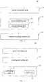
- Fig. 1is a block diagram of a second adapter according to an embodiment of the present disclosure.
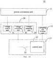
- the second adapter 10 in Fig. 1includes a power conversion unit 11, a sampling and holding unit 12 and a current sampling control unit 13.
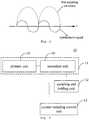
- the power conversion unit 11is configured to convert input alternating current to obtain an output voltage and an output current of the second adapter 10.
- the output current of the second adapter 10is a current with a first pulsating waveform.
- the sampling and holding unit 12is coupled with the power conversion unit 11. When the sampling and holding unit 12 is in a sampling state, the sampling and holding unit 12 is configured to sample the current with the first pulsating waveform. When the sampling and holding unit 12 is in a holding state, the sampling and holding unit 12 is configured to hold (or lock) a peak value of the current with the first pulsating waveform.
- the current sampling control unit 13is coupled with the sampling and holding unit 12.
- the current sampling control unit 13is configured to determine whether the sampling and holding unit 12 is in the holding state, and to sample the peak value of the current with the first pulsating waveform held by the sampling and holding unit 12 when determining that the sampling and holding unit 12 is in the holding state.
- the output current of the second adapteris the current with the pulsating waveform (or referred to as the pulsating direct current), which can reduce the lithium precipitation of the battery.
- the current with the pulsating waveformcan reduce a probability and intensity of arc of a contact of a charging interface, and can prolong a service life of the charging interface.
- the second adaptermay adjust the output current of itself according to actual situations. Taking the second adapter supporting the constant current mode as an example, the second adapter may typically continuously adjust the output current of itself based on the voltage of the battery in the device to be charged such as the terminal, to charge the battery in a multi-stage constant current mode. Thus, during the charging process, it requires to detect and control the output current of the second adapter in real time. When the current value of the output current of the second adapter is constant, it is easy to realize the detection and control of the output current of the second adapter.
- the output current of the second adapteris the current having the first pulsating waveform, a magnitude of which is varying, and thus it is required to design a special way for detecting and controlling the output current of the second adapter.
- the sampling and holding unit 12 and the current sampling control unit 13are introduced. Based on the sampling and holding unit 12 and the current sampling control unit 13, the peak value of the output current of the second adapter can be sampled, and thus the efficient control on the output current of the second adapter can be ensured.
- the output current of the second adapteris the current with the first pulsating waveform.
- the pulsating waveformmay refer to an entire pulsating waveform, or may refer to a pulsating waveform obtained after performing a peak clipping process on the entire pulsating waveform.
- the peak clipping processmay refer to filtering out a portion of the pulsating waveform which exceeds a certain threshold, thus realizing the control on the peak value of the pulsating waveform.
- the pulsating waveformis an entire pulsating waveform.
- the pulsating waveformis obtained after performing a peak clipping process.
- the method in which the power conversion unit 11 converts the alternating current into the current with the first pulsating waveformis not limited.
- a primary filtering unit and a secondary filtering unit in the power conversion unit 11may be omitted, such that the current with the first pulsating waveform is generated.
- the device to be charged used in embodiments of the present disclosuremay be a communication terminal (or short for a terminal), which includes, but is not limited to a device configured to receive/transmit communication signals via a wired connection (for example, public switched telephone network (PSTN), digital subscriber line (DSL) connection, digital cable connection, direct cable connection and/or another data connection/network) and/or via a wireless interface (for example, cellular network, wireless local area network (WLAN), digital TV network such as digital video broadcasting handheld (DVB-H) network, satellite network, an amplitude modulation-frequency modulation (AM-FM) broadcasting transmitter, and/or a wireless interface of another communication terminal).
- a wired connectionfor example, public switched telephone network (PSTN), digital subscriber line (DSL) connection, digital cable connection, direct cable connection and/or another data connection/network
- a wireless interfacefor example, cellular network, wireless local area network (WLAN), digital TV network such as digital video broadcasting handheld (DVB-H) network, satellite network, an
- the communication terminal configured to communicate via the wireless interfacemay be referred to as "wireless communication terminal", “wireless terminal” and/or “mobile terminal”.
- a mobile terminalinclude, but are not limited to a satellite phone or a cell phone, a terminal combining a cell radio phone and a personal communication system (PCS) having capability of data process, fax, and data communication, a personal digital assistant (PDA) including a radio phone, a pager, Internet/Intranet access, a web browser, a note pad & address book, a calendar and/or a global positioning system (GPS) receiver, and a common laptop and/or handheld receiver, or other electronic devices including a radio phone transceiver.
- PCSpersonal communication system
- PDApersonal digital assistant
- GPSglobal positioning system
- the second adapter 10may include a charging interface (refer to the charging interface 191 illustrated in Fig. 19A ) .
- a type of the charging interfaceis not limited.
- the charging interfacemay be a universal serial bus (USB) interface, which may be a common USB interface or a micro USB interface, or a Type-C interface.
- USBuniversal serial bus
- the implementation of the sampling and holding unit 12is not limited. Typically, the sampling and holding unit 12 can realize signal sampling and holding based on a capacitor. In the following, the implementation of the sampling and holding unit 12 will be described in detail with reference to Fig. 3 .
- the sampling and holding unit 12may include a current sampling unit 14 and a current holding unit 15.
- the current sampling unit 14is coupled with the power conversion unit 11, and is configured to detect the current with the first pulsating waveform to obtain a sampling current, and to convert the sampling current into a sampling voltage.
- the sampling voltageis configured to indicate a magnitude of the current with the first pulsating waveform.
- the current holding unit 15is coupled with the current sampling unit 14 and the current sampling control unit 13 respectively.
- the current holding unit 15receives the sampling voltage from the current sampling unit 14, and charges a capacitor (not illustrated in Fig. 3 ) in the current holding unit 15 based on the sampling voltage.
- the current sampling control unit 13obtains the peak value of the current with the first pulsating waveform by sampling the voltage across both ends of the capacitor in the current sampling control unit 13.
- the capacitor in the current holding unit 15increases with the current value of the current with the first pulsating waveform, and the sampling and holding unit 12 is in the sampling state.
- the voltage across both ends of the capacitor in the current holding unit 15keeps constant, and the sampling and holding unit 12 is in the holding state.
- the peak value of the current with the first pulsating waveform held by the sampling and holding unit 12is sampled by the current sampling control unit 13.
- the current sampling control unit 13may include an ADC (Analog-to-Digital Converter), and the current sampling control unit 13 may sample the peak value of the current with the first pulsating waveform based on the ADC.
- the current sampling control unit 13may further include a control unit.
- the control unitmay be, for example, a MCU (Microcontroller Unit).
- the control unitincludes an ADC port, and the control unit may be coupled to the capacitor in the sampling and holding unit 12 via the ADC port.
- the control unitmay sample the peak value of the current with the first pulsating waveform by sampling the voltage across both ends of the capacitor.
- the sampling and holding unit 12When the sampling and holding unit 12 is in the sampling state, the voltage across both ends of the capacitor increases with the current value of the current with the first pulsating waveform, which is equivalent to a charging process. When the sampling and holding unit 12 is in the holding state, the voltage across both ends of the capacitor reaches the maximum. A correspondence relationship between the voltage across both ends of the capacitor and the current value of the first pulsating waveform can be established in advance. In this way, the current sampling control unit 13 can obtain the peak value of the current with the first pulsating waveform by sampling the voltage value across both ends of the capacitor.
- the current sampling control unit 13is further configured to control the sampling and holding unit 12 to switch to the sampling state from the holding state, after the peak value of the current with the first pulsating waveform is sampled.
- the peak value of the current with the first pulsating waveformmay vary in real time, and thus it is required to continuously detect the peak value of the current with the first pulsating waveform, so as to ensure the real-time performance and accuracy of the current information, and further ensure smooth proceeding of the whole charging process.
- the current sampling control unit 13provided by embodiments of the present disclosure may control the sampling and holding unit 12 to enter into the sampling state, to re-sample the current with the first pulsating waveform, thus ensuring the real-time performance and accuracy of the sampled peak value of the current with the first pulsating waveform.
- the current sampling control unit 13may complete one sampling of the peak value in each cycle of the first pulsating waveform, and control the sampling and holding unit 12 to switch to the sampling state from the holding state immediately after sampling the peak value. In this way, the peak value of the current with the first pulsating waveform sampled by the current sampling control unit 13 is updated every cycle of the first pulsating waveform, thus ensuring the real-time performance and accuracy of the sampled peak value of the current with the first pulsating waveform.
- the output current of the second adapter 10, i.e., the charging currentis the current with the first pulsating waveform.
- the charging currentmay charge the battery intermittently, and a cycle of the charging current may vary with the gird frequency.
- the frequency corresponding to the cycle of the charging currentmay be an integral multiple of the grid frequency, or may be 1/N of the grid frequency, where N is an integer greater than 1.
- the charging currentmay charge the battery intermittently.
- the charging currentmay consist of one pulse or a set of pulses synchronous with the power grid.
- the current sampling control unit 13may control the sampling and holding unit 12 to switch to the sampling state from the holding state in many ways.
- the current sampling control unit 13may control the capacitor in the sampling and holding unit 12 to discharge, to empty charges in the capacitor, such that when a next sampling cycle comes, the capacitor in the sampling and holding unit 12 may be charged again.
- the sampling and holding unit 12may hold the peak value of the current with the first pulsating waveform based on the capacitor (not illustrated in Fig. 4 ) in the sampling and holding unit 12.
- the current sampling control unit 13may include a discharging unit 16 and a control unit 17.
- the discharging unit 16is coupled to the control unit 17 and the capacitor in the sampling and holding unit 12 respectively.
- the discharging unit 16is configured to release charges in the capacitor of the sampling and holding unit 12 under a control of the control unit 17, such that the sampling and holding unit 12 switches to the sampling state from the holding state.
- the peak value of the current with the first pulsating waveform held by the sampling and holding unit 12may be sampled by the control unit 17.
- the discharging unit 16may be implemented in many ways.
- the discharging unit 16may include a switch and a resistor coupled in series with the capacitor in the sampling and holding unit 12.
- the control unit 17controls the switch to switch on, such that the capacitor discharges to the resistor, thus releasing the charges in the capacitor.
- the way in which the current sampling control unit 13 determines whether the sampling and holding unit 12 is in the holding stateis not limited, which will be described in detail below with reference to specific embodiments.
- the current sampling control unit 13may detect the current value sampled by the sampling and holding unit 12 in real time, and when the current values detected twice in a row keep being unchanged, it indicates that the sampling and holding unit 12 is in the holding state.
- the current sampling control unit 13is configured to receive a synchronous signal, and to determine whether the sampling and holding unit 12 is in the holding state based on the synchronous signal.
- a cycle of the synchronous signalis 1/N of the cycle of the first pulsating waveform, where N is an integer greater than or equal to 1.
- the time interval between the sampling state and the holding state of the sampling and holding unit 12is related to the cycle of the current with the first pulsating waveform (this time interval may be 1/2 of the cycle of the current with the first pulsating waveform).
- the synchronous signal having a special relationship with the cycle of the first pulsating waveformis introduced (i.e., the cycle of the synchronous signal is 1/N of the cycle of the first pulsating waveform), and the working state of the sampling and holding unit 12 is determined based on the synchronous signal.
- the cycle relationship and/or phase relationship of the synchronous signal and the first pulsating waveformmay be used to determine whether the first pulsating waveform is at the peak value or in the falling edge.
- the first pulsating waveformis at the peak value or in the falling edge, it is determined that the sampling and holding unit 12 is in the holding state .
- determining whether the first pulsating waveform is at the peak value or in the falling edgerefers to determining whether the first pulsating waveform is at the peak value of the first pulsating waveform or in the falling edge of the first pulsating waveform.
- determining whether the first pulsating waveform is at the peak value or in the falling edgerefers to determining whether the present output current of the second adapter is at the peak value of the first pulsating waveform or in the falling edge of the first pulsating waveform, or determining whether the present output current of the second adapter is the current corresponding to the peak value or the falling edge of the first pulsating waveform.
- the cycle of the first pulsating waveformis the same as the cycle of the synchronous signal.
- the first pulsating waveformmay be in phase with the synchronous signal. In other words, when the synchronous signal is in the rising edge, the first pulsating waveform is in the rising edge, and when the synchronous signal is at the peak value or in the falling edge, the first pulsating waveform is at the peak value or in the falling edge.
- the sampling and holding unitSince the sampling and holding unit is in the holding state when the first pulsating waveform is at the peak value or in the falling edge, it is possible to determine the time when the sampling and the holding unit 12 is in the holding state as long as the time when the synchronous signal is at the peak value or in the falling edge is determined.
- the cycle of the synchronous signalis 1/2, 1/3, 1/4 and the like of the cycle of the first pulsating waveform
- the waveform of the synchronous signalis presented by solid line
- the first pulsating waveformis presented by dotted line.
- the cycle of the synchronous signalis 1/2 of the cycle of the first pulsating waveform, and thus when the synchronous signal is in the negative half-cycle, the first pulsating waveform is at the peak value or in the falling edge, and the sampling and holding unit 12 is in the holding state.
- it is possible to determine when the first pulsating waveform is at the peak value or in the falling edgeby only determining when the waveform of the synchronous signal is in the negative half-cycle. And similarly for the others, which will not be elaborated here.
- the synchronous signalmay be with the pulsating waveform, or with the triangular waveform, or may be of other types, which is not limited in embodiments of the present disclosure.
- the way for obtaining the synchronous signalis not limited, which will be described in detail below with reference to specific embodiments.
- the current sampling control unit 13is coupled to the power conversion unit 11, and configured to obtain the synchronous signal from the power conversion unit 11.
- the synchronous signal obtained from the power conversion unit 11may be the alternating current signal received by the power conversion unit 11, the voltage/current signal obtained by the power conversion unit 11 after primary rectification, or the voltage/current signal coupled to the secondary side from the primary side of the power conversion unit 11, or the voltage/current signal obtained after secondary rectification, or the like, which is not limited in embodiments of the present disclosure.
- the power conversion unit 11may include a primary unit 18 and a secondary unit 19.
- the current sampling control unit 13is coupled to the secondary unit 19, and configured to obtain the synchronous signal from the secondary unit 19.
- the synchronous signalmay be obtained directly from the bus (VBUS) of the secondary unit 19.
- the output current of the second adapter 10is the current with the first pulsating waveform, and the output end of the second adapter 10 is coupled with the bus of the secondary unit 19, it should have the current with the first pulsating waveform on the bus of the secondary unit 19, and the synchronous signal can be obtained directly from the bus of the secondary unit 19.
- the secondary unit 19may include a first rectifier unit 20.
- the first rectifier unit 20is coupled to the current sampling control unit 13.
- the first rectifier unit 20is configured to rectify the current coupled to the secondary unit 19 from the primary unit 18, to obtain a voltage with a second pulsating waveform, and to send the voltage with the second pulsating waveform to the current sampling control unit 13 as the synchronous signal.
- the secondary unit 19itself includes a secondary rectifier unit.
- the secondary rectifier unit and the first rectifier unit 20may be two separate rectifier units.
- the secondary rectifier unitis configured to rectify the current coupled to the secondary side from the primary side, to obtain the output current of the second adapter.
- the first rectifier unitis configured to rectify the current coupled to the secondary side from the primary side, to obtain the synchronous signal.
- the unit indicated by the reference number 39is the secondary rectifier unit. Both the secondary rectifier unit 39 and the first rectifier unit 20 may be located close to the secondary winding side of the transformer Tl, so as to rectify the current coupled to the secondary side from the primary side.
- the power conversion unit 11may include a primary unit 18 and a secondary unit 19.
- the current sampling control unit 13is coupled to the primary unit 18, and configured to obtain the synchronous signal from the primary unit 18.
- the synchronous signalthere may be many ways for obtaining the synchronous signal from the primary unit 18. For example, it is possible to obtain the alternating current signal directly from the primary unit 18 and send the alternating current signal to the current sampling control unit 13 as the synchronous signal. For another example, the pulsating direct current signal obtained after rectification of the rectifier circuit in the primary unit 18 may be sent to the current sampling control unit 13 as the synchronous signal.
- the primary unit 18rectifies the alternating current AC to obtain a voltage with the third pulsating waveform.
- the cycle of the third pulsating waveformis the same as the cycle of the first pulsating waveform.
- the primary unit 18may couple the voltage with the third pulsating waveform to the secondary side from the primary side of the second adapter 10 via an optical coupling unit 21 to obtain a voltage with a fourth pulsating waveform, and send the voltage with the fourth pulsating waveform to the current sampling control unit 13 as the synchronous signal.
- the optical coupling unit 21may play a function of isolating interference between the primary side and the secondary side.
- the primary unit 18may directly send the voltage with the third pulsating waveform to the current sampling control unit 13 without passing through the optical coupling unit 21, which is not limited in embodiments of the present disclosure.
- the way for obtaining the synchronous signal from the power conversion unit 11is described in detail with reference to specific embodiments .
- the way for obtaining the synchronous signalis not limited to this, and other ways for obtaining the synchronous signal are illustrated in the following.
- the current sampling control unit 13may obtain the synchronous signal from the sampling and holding unit 12.
- the sampling and holding unit 12may sample the output current of the second adapter, i.e. , the current with the first pulsating waveform, to obtain the sampling current.
- the sampling current obtained by the sampling and holding unit 12, or signals such as the sampling voltage corresponding to the sampling currenthave a same cycle and phase as the current with the first pulsating waveform.
- Using the sampling current or sampling voltage as the synchronous signalmay simplify the logic of determining the working state of the sampling and holding unit 12.
- the sampling and holding unit 12will sample the current with the first pulsating waveform to obtain the sampling current, and convert the sampling current into the sampling voltage.
- the sampling voltagemay be used to indicate the magnitude of the current with the first pulsating waveform.
- the sampling and holding unit 12may send the sampling voltage to the current sampling control unit 13 as the synchronous signal.
- the voltage signal outputted from the output port (OUTPUT) of the galvanometermay be used as the synchronous signal.
- the current sampling control unit 13determines whether the first pulsating waveform is at the peak value or in the falling edge based on the synchronous signal, and samples the peak value of the current with the first pulsating waveform held by the sampling and holding unit 12 when determining that the first pulsating waveform is at the peak value or in the falling edge.
- the sampling and holding unit 12may switch between the sampling state and the holding state based on charging and discharging of the capacitor.
- the first pulsating waveformWhen the first pulsating waveform is in the rising edge, the capacitor in the sampling and holding unit 12 is in the charging state, the voltage across both ends of the capacitor increases with the current with the first pulsating waveform, and at this time, the sampling and holding unit 12 is in the sampling state.
- the first pulsating waveformis at the peak value or in the falling edge, the voltage across both ends of the capacitor does not increase anymore, and at this time, the sampling and holding unit 12 is in the holding state.
- the phase and cycle of the synchronous signalcan be determined based on the phase and/or cycle of the synchronous signal. For example, the synchronous signal is in phase with the first pulsating waveform, and when the synchronous signal is at the peak value or in the falling edge, the first pulsating waveform is at the peak value or in the falling edge.
- the cycle of the synchronous signalis the same as the cycle of the first pulsating waveform, and the phase difference between the synchronous signal and the first pulsating waveform is a half cycle, and when the synchronous signal is in the rising edge, the first pulsating waveform is at the peak value or in the falling edge.
- the current or voltage of the synchronous signalmay be detected in real time by an amperemeter or a voltmeter, such that the phase of the synchronous signal is determined, and further whether the first pulsating waveform is at the peak value or in the falling edge is determined.
- this wayneeds an additional current and voltage detecting circuit, which is complicated to implement.
- two implementations based on a comparatorare described, which may compare the voltage of the synchronous signal with a reference voltage, so as to conveniently determine whether the first pulsating waveform is at the peak value or in the falling edge.
- the current sampling control unit 13may include a comparator 22 and a control unit 23.
- a first input end of the comparator 22is configured to receive the synchronous signal, and a second input end of the comparator 22 is configured to receive a reference voltage.
- the control unit 23is coupled to an output end of the comparator 22, and configured to determine whether the first pulsating waveform is at the peak value or in the falling edge based on a comparison result between the voltage of the synchronous signal and the reference voltage.
- the first input endis a non-inverting input end of the comparator, and the second input end is an inverting input end of the comparator.
- the first input endis the inverting input end of the comparator, and the second input end is the non-inverting input end of the comparator.
- the way for selecting the voltage value of the reference voltageis not limited. Taking the synchronous signal being a pulsating signal at zero crossing point as an example, the voltage value of the reference voltage may be selected as a certain value greater than zero and less than the peak value of the synchronous signal. Taking the synchronous signal being the alternating current signal as an example, the voltage value of the reference voltage may be selected as zero.
- the way for determining whether the first pulsating waveform is at the peak value or in the falling edge based on the comparison result between the voltage of the synchronous signal and the reference voltageis not limited. This determining is related to the cycle and phase of the synchronous signal and the cycle and phase of the first pulsating waveform.
- the way for determining the peak value or falling edge of the first pulsating waveformis illustrated. In embodiments of Fig. 11 and Fig.
- the current sampling control unit 13samples the peak value of the current with the first pulsating waveform held by the sampling and holding unit in each cycle of the first pulsating waveform. After the sampling is completed, the current sampling control unit 13 immediately provides the control voltage to a MOS transistor in the discharging unit, controls the MOS transistor in the discharging unit to switch on, and releases the charges in the capacitor of the sampling and holding unit 12.
- Fig. 11 and Fig. 12are merely examples, and the present disclosure is not limited thereto.
- the current sampling control unit 13may sample the peak value of the current with the first pulsating waveform once every multiple cycles.
- the discharging unitmay be implemented in ways other than using the MOS transistor, for example, the discharging unit may be controlled to switch on and off by using other types of switches.
- the synchronous signalis in phase with the first pulsating waveform (the pulsating waveform after the peak clipping process). It can be seen from Fig. 11 that, since the synchronous signal is in phase with the first pulsating waveform, the first pulsating waveform is at the peak value or in the falling edge when the synchronous signal is at the peak value or in the falling edge. Thus, as long as when the synchronous signal is at the peak value or in the falling edge is determined, when the first pulsating waveform is at the peak value or in the falling edge can be obtained.
- a comparatoris introduced in the embodiment of Fig. 11 .
- the comparatorobtains a changing curve of an output level of itself (i.e. , the rectangular wave as illustrated in Fig. 11 ) by comparing the voltage values of the synchronous signal and the reference voltage. It can be seen from the rectangular wave that, at the moment when the output level of the comparator switches to the low level from the high level (hereinafter, referred to as the target moment), the first pulsating waveform is in the falling edge. At this moment, the capacitor in the sampling and holding unit 12 is in the holding state.
- the target momentis used as the peak value sampling point
- the current sampling control unit 13is controlled to sample the voltage across both ends of the capacitor in the sampling and holding unit 12, and further the peak value of the current with the first pulsating waveform is obtained.
- the MOS transistor in the discharging unitis immediately controlled to switch on, such that the charge in the capacitor of the sampling and holding unit 12 is released, and the sampling in a next cycle is prepared.
- the phase difference between the synchronous signal and the first pulsating waveformis 180 degree, and the first pulsating waveform is subjected to the peak clipping process. It can be seen from Fig. 12 that, since the phase difference between the synchronous signal and the first pulsating waveform is 180 degree, the first pulsating waveform is at the peak value or in the falling edge when the synchronous signal is at the peak value or in the rising edge. Thus, as long as when the synchronous signal is at the peak value or in the rising edge is determined, when the first pulsating waveform is at the peak value or in the falling edge can be obtained.
- a comparatoris introduced into the embodiment of Fig. 12 .
- the comparatorobtains a changing curve of an output level of itself (i.e. , the rectangular wave as illustrated in Fig. 12 ) by comparing the voltage values of the synchronous signal and the reference voltage. It can be seen from the rectangular wave that, at the moment when the output level of the comparator switches to the high level from the low level (hereinafter, referred to as the target moment), the first pulsating waveform is in the falling edge. At this moment, the capacitor in the sampling and holding unit 12 is in the holding state.
- the target momentis used as the peak value sampling point
- the current sampling control unit 13is controlled to sample the voltage across both ends of the capacitor in the sampling and holding unit 12, and further the peak value of the current with the first pulsating waveform is obtained.
- the MOS transistor in the discharging unitis immediately controlled to switch on, such that the charge in the capacitor of the sampling and holding unit 12 is released, and the sampling in a next cycle is prepared.
- the current sampling control unit 13may include a comparing unit 24 and a control unit 25.
- the comparing unit 24may include a capacitor 26 and a comparator 27.
- the capacitor 26is configured to receive the synchronous signal, and to filter out a direct current signal in the synchronous signal to obtain an alternating current signal at zero crossing point.
- a first input end of the comparator 27is coupled to the capacitor 26, and is configured to receive the alternating current signal.
- a second input end of the comparator 27is configured to receive the reference voltage.
- the comparator 27is configured to compare the voltage of the alternating current signal with the reference voltage.
- the control unit 25is coupled to an output end of the comparator 27, and is configured to determine whether the first pulsating waveform is at the peak value or in the falling edge based on the comparison result between the voltage of the alternating current signal and the reference voltage. Further, in embodiments of the present disclosure, the voltage value of the reference voltage can be set to zero.
- the first input endis a non-inverting input end of the comparator, and the second input end is an inverting input end of the comparator. In other embodiments, the first input end is the inverting input end of the comparator, and the second input end is the non-inverting input end of the comparator.
- the signal with the pulsating waveformcan be regarded as being formed of a direct current signal (direct current component) and an alternating current signal at zero crossing point (alternating current component).
- the capacitor 26can filter out the direct current signal in the signal with the pulsating waveform, and the alternating current signal at zero crossing point remains.
- the reference voltage of the comparator 27to zero (for example, the second input end of the comparator is grounded), the phase of the synchronous signal can be determined easily.
- the second adapter 10may further include a voltage adjusting unit 28.
- the voltage adjusting unit 28is coupled to the power conversion unit 11, and is configured to detect and adjust the output voltage of the second adapter 10.
- the current sampling control unit 13is coupled to the voltage adjusting unit 28. The peak value of the current with the first pulsating waveform is adjusted by the voltage adjusting unit 28.
- the basic function of the voltage adjusting unit 28is to adjust the output voltage of the second adapter.
- the voltage adjusting unit 28may detect the output voltage of the second adapter 10 via the power conversion unit 11, and adjust the output voltage of the second adapter 10 via the power conversion unit 11.
- the voltage adjusting unit 28 and the power conversion unit 11form a feedback control system of the output voltage of the second adapter, in which the feedback control system may be referred to as a voltage feedback loop. It should be understood that, when the output power of the second adapter is fixed, adjusting the voltage will cause changing of the current.
- the current sampling control unit 13may utilize the above voltage feedback loop to realize adjusting the current. For example, after the current sampling control unit 13 samples the peak value of the current with the first pulsating waveform, if the current sampling control unit 13 wishes to adjust the sampled peak value of the current with the first pulsating waveform to a target peak value, the current sampling control unit 13 may calculate a target value of the output voltage of the second adapter 10 corresponding to the target peak value via software, and then adjust the output voltage of the second adapter 10 to the target value by using the voltage feedback loop.
- the current sampling control unit 13 and the voltage feedback loopform the feedback control system for the peak value of the output current of the second adapter 10.
- the feedback control systemis also referred to as the current feedback loop.
- itdoes not only include the voltage feedback loop (implemented by hardware), but also include the current feedback loop (based on the voltage feedback loop, and implemented by software calculation), such that the second adapter can realize not only controlling the output voltage of the second adapter, but can also realize controlling the output current of the second adapter, which riches the functions of the second adapter, and improves the intelligence degree of the second adapter.
- the voltage adjusting unit 28may include a voltage sampling unit 29, a voltage comparing unit 30 and a voltage control unit 31.
- the voltage sampling unit 29is coupled to the power conversion unit 11, and is configured to sample the output voltage of the second adapter 10 to obtain a first voltage.
- An input end of the voltage comparing unit 30is coupled to the voltage sampling unit 29, and the voltage comparing unit 30 is configured to compare the first voltage with a first reference voltage.
- An input end of the voltage control unit 31is coupled to an output end of the voltage comparing unit 30.
- An output end of the voltage control unit 31is coupled to the power conversion unit 11.
- the voltage control unit 31controls the output voltage of the second adapter 10 according to the comparison result of the first voltage and the first reference voltage.
- the current sampling control unit 13is coupled to the voltage comparing unit 30, and is configured to adjust the peak value of the current with the first pulsating waveform by adjusting the voltage value of the first reference voltage.
- the input end of the voltage sampling unit 29may be coupled to the bus (VBUS) of the second adapter, for sampling the output voltage of the second adapter.
- the voltage sampling unit 29may be a wire.
- the first voltage sampled by the voltage sampling unit 29is the output voltage of the second adapter.
- the voltage sampling unit 29may include two resistors configured for voltage division. In this way, the first voltage sampled by the voltage sampling unit 29 is the voltage obtained after voltage division by the two resistors .
- the voltage comparing unit 30is implemented by an operational amplifier. One input end of the operational amplifier is configured to receive the first voltage inputted by the voltage sampling unit 29, and the other input end of the operational amplifier is configured to receive the first reference voltage.
- An output end of the operational amplifieris configured to generate a voltage feedback signal, for indicating whether the first voltage is equal to the first reference voltage.
- the voltage control unit 31may be implemented based on elements such as an optical coupling element and a PWM controller, and may adjust the output voltage of the second adapter based on the voltage feedback signal provided by the voltage comparing unit 30.
- the current sampling control unit 13may calculate the expected value of the output voltage of the second adapter based on the expected peak value of the current with the first pulsating waveform.
- the output voltage of the second adapteris adjusted to the expected value of the output voltage of the second adapter, such that the peak value of the current with the first pulsating waveform is adjusted to the expected peak value.
- the current sampling control unit 13may include a control unit 32 and a DAC (Digital-to-Analog Converter) 33.
- An input end of the DAC 33is coupled to the control unit 32, and an output end of the DAC 33 is coupled to the voltage comparing unit 30.
- the control unit 32adjusts the voltage value of the first reference voltage via the DAC 33, so as to adjust the peak value of the current with the first pulsating waveform.
- the control unit 32may adjust the voltage value of the first reference voltage via circuits such as an RC unit and a digital potentiometer, which is not limited in embodiments of the present disclosure.
- the voltage adjusting unit 28may include a voltage dividing unit 34, a voltage comparing unit 30 and a voltage control unit 31.
- An input end of the voltage dividing unit 34is coupled to the power conversion unit 11.
- the voltage dividing unit 34is configured to perform voltage division on the output voltage of the second adapter 10 based on a preset voltage division ratio to obtain a second voltage.
- An input end of the voltage comparing unit 30is coupled to an output end of the voltage dividing unit 34 .
- the voltage comparing unit 30is configured to compare the second voltage with a second reference voltage.
- An input end of the voltage control unit 31is coupled to the input end of the voltage comparing unit 30.
- An output end of the voltage control unit 31is coupled to the power conversion unit 11.
- the voltage control unit 31controls the output voltage of the second adapter 10 according to the comparison result of the second voltage and the second reference voltage.
- the current sampling control unit 13is coupled to the voltage comparing unit 30, and is configured to adjust the peak value of the current with the first pulsating waveform by adjusting the voltage division ratio.
- This embodimentis similar to the embodiment of Fig. 15 , and the difference lies in that the voltage dividing unit is introduced in this embodiment.
- the voltage division ratio of the voltage dividing unitis adjustable.
- the current sampling control unit 13does not adjust the peak value of the current with the first pulsating waveform by adjusting the reference voltage of the voltage comparing unit 30. Instead, the current sampling control unit 13 adjusts the peak value of the current with the first pulsating waveform by adjusting the voltage division ratio of the voltage dividing unit 34.
- itbased on the voltage dividing unit, it does not only realize sampling the output voltage of the second adapter, but also realize adjusting the peak value of the current with the first pulsating waveform, which simplifies the circuit structure of the second adapter.
- the reference voltage of the voltage comparing uniti.e. , the second reference voltage
- the reference voltage of the voltage comparing unitmay be a fixed value.
- the above voltage division function and the function of adjusting the voltage division ratiocan be achieved by the digital potentiometer or by elements such as separate resistors and switches.
- the current sampling control unit 13includes a control unit 32, and the voltage dividing unit 34 includes a digital potentiometer 35.
- a high level end of the digital potentiometer 35is coupled to the power conversion unit 11.
- a low level end of the digital potentiometer 35is grounded.
- An output end of the digital potentiometer 35is coupled to the voltage comparing unit 30.
- the control unit 32is coupled to a control end of the digital potentiometer 35, and is configured to adjust the voltage division ratio of the digital potentiometer 35 via the control end of the digital potentiometer 35, so as to adjust the peak value of the current with the first pulsating waveform.
- the second adapter 10may support a first charging mode and a second charging mode.
- the charging speed of the second adapter 10 charging the device to be charged (such as the terminal) in the second charging modeis greater than the charging speed of the second adapter 10 charging the device to be charged (such as the terminal) in the first charging mode (the above current with the first pulsating waveform may be the output current of the second adapter in the second charging mode) .
- the second adapter 10 working in the second charging modecan fully charge the battery having the same capacity in the device to be charged (such as the terminal) in a shorter time.
- the second adapter 10includes a control unit. During the connection of the second adapter 10 and the device to be charged (such as the terminal), the control unit performs a bidirectional communication with the device to be charged (such as the terminal), thus controlling the charging process of the second charging mode.
- the control unitmay be as described in the above embodiments, for example, may be the control unit in the first adjusting unit, or the control unit in the second adjusting unit.
- the first charging modecan be a normal charging mode and the second charging mode can be a quick charging mode.
- the second adapterUnder the normal charging mode, the second adapter outputs a relatively small current (typically less than 2.5 A) or charges the battery in the device to be charged (such as the terminal) with a relatively small power (typically less than 15 W). In the normal charging mode, it may take several hours to fully charge a larger capacity battery (such as a battery with 3000 mAh).
- the second adaptercan output a relatively large current (typically greater than 2.5A, such as 4.5A, 5A or higher) or charges the battery in the device to be charged (such as the terminal) with a relatively large power (typically greater than or equal to 15W) .
- the charging speed of the second adapter in the quick charging modeis faster, and the charging time required for fully charging a battery with the same capacity in the quick charging mode may be significantly shortened.
- the content communicated between the control unit of the second adapter and the device to be chargedis not limited in embodiments of the present disclosure, and the control manner of the control unit on the output of the second adapter in the second charging mode is also not limited in embodiments of the present disclosure.
- the control unitmay communicate with the device to be charged (such as the terminal) to exchange the present voltage or the present electric quantity of the battery in the device to be charged (such as the terminal), and adjust the output voltage or output current of the second adapter based on the present voltage or the present electric quantity of the battery.
- the content communicated between the control unit and the device to be charged (such as the terminal) and the control manner of the control unit on the output of the second adapter in the second charging modewill be described in detail in combination with specific embodiments.
- control unitperforms the bidirectional communication with the device to be charged (such as the terminal) to control the output of the second adapter in the second charging mode as follows.
- the control unitperforms the bidirectional communication with the device to be charged (such as the terminal) to negotiate the charging mode between the second adapter and the device to be charged (such as the terminal).
- the second adapterdoes not quickly charge the device to be charged (such as the terminal) in the second charging mode blindly. Instead, the second adapter performs the bidirectional communication with the device to be charged (such as the terminal) to negotiate whether the second adapter can quickly charge the device to be charged (such as the terminal) in the second charging mode, thus improving the safety of the charging process.
- control unitperforms the bidirectional communication with the device to be charged (such as the terminal) to negotiate the charging mode between the second adapter and the device to be charged (such as the terminal) as follows.
- the control unitsends a first instruction to the device to be charged (such as the terminal), in which the first instruction is configured to query the device to be charged (such as the terminal) whether to operate in the second charging mode.
- the control unitreceives a reply instruction of the first instruction from the device to be charged (such as the terminal), in which the reply instruction of the first instruction is configured to indicate whether the device to be charged (such as the terminal) agrees to operate in the second charging mode.
- the control unitcharges the device to be charged (such as the terminal) in the second charging mode when the device to be charged (such as the terminal) agrees to operate in the second charging mode.
- the master-slave relation of the second adapter (or the control unit of the second adapter) and the device to be charged (such as the terminal)is not limited in embodiments of the present disclosure.
- any of the control unit and the device to be charged (such as the terminal)can be configured as the master device initiating the bidirectional communication session, accordingly, the other one can be configured as the slave device making a first response or a first reply to the communication initiated by the master device .
- the identifications of the master device and the slave devicecan be determined by comparing the electrical levels of the second adapter and the device to be charged (such as the terminal) relative to the ground.
- any of the second adapter (or the control unit of the second adapter) and the device to be charged (such as the terminal)can be configured as the master device initiating the communication session, accordingly, the other one can be configured as the slave device making a first response or a first reply to the communication session initiated by the master device, and the master device is able to make a second response to the first response or the first reply of the slave device, and thus a negotiation about a charging mode can be realized between the master device and the slave device.
- a charging operation between the master device and the slave deviceis performed after a plurality of negotiations about the charging mode are completed between the master device and the slave device, such that the charging process can be performed safely and reliably after the negotiation.
- the master deviceis able to make a second response to the first response or the first reply made by the slave device with regard to the communication session in a manner that, the master device is able to receive the first response or the first reply made by the slave device to the communication session and to make a targeted second response to the first response or the first reply.
- the master devicewhen the master device receives the first response or the first reply made by the slave device to the communication session in a predetermined time period, the master device makes the targeted second response to the first response or the first reply of the slave device in a manner that, the master device and the slave device complete one negotiation about the charging mode, and a charging process may be performed between the master device and the salve device in the first charging mode or the second charging mode according to a negotiation result, i.e. , the second adapter charges the device to be charged (such as the terminal) in the first charging mode or the second charging mode according to a negotiation result.
- a negotiation resulti.e. , the second adapter charges the device to be charged (such as the terminal) in the first charging mode or the second charging mode according to a negotiation result.
- the master deviceis able to make a second response to the first response or the first reply made by the slave device to the communication session in a manner that, when the master device does not receive the first response or the first reply made by the slave device to the communication session in the predetermined time period, the masterdevice also makes the targeted second response to the first response or the first reply of the slave device.
- the masterdevicewhen the master device does not receive the first response or the first reply made by the slave device to the communication session in the predetermined time period, the masterdevice makes the targeted second response to the first response or the first reply of the slave device in a manner that, the master device and the slave device complete one negotiation about the charging mode, the charging process is performed between the masterdevice and the slave device in the first charging mode, i.e., the second adapter charges the device to be charged (such as the terminal) in the first charging mode.
- the device to be charged(such as the terminal) is configured as the masterdevice initiating the communication session
- the second adapter (or the control unit of the second adapter) configured as the slave devicemakes the first response or the first reply to the communication session initiated by the master device
- one negotiation about the charging modeis regarded as completed between the second adapter (or the control unit of the second adapter) and the device to be charged (such as the terminal)
- the second adapteris able to charge the device to be charged (such as the terminal) in the first charging mode or the second charging mode according to the negotiation result.
- control unitperforms the bidirectional communication with the device to be charged (such as the terminal) to control the output of the second adapter in the second charging mode as follows.
- the control unitperforms the bidirectional communication with the device to be charged (such as the terminal) to determine a charging voltage outputted by the second adapter in the second charging mode for charging the device to be charged (such as the terminal) .
- the control unitadjusts the output voltage of the second adapter, such that the output voltage of the second adapter is equal to the charging voltage outputted by the second adapter in the second charging mode for charging the device to be charged (such as the terminal).
- control unitperforms the bidirectional communication with the device to be charged (such as the terminal) to determine the charging voltage outputted by the second adapter in the second charging mode for charging the device to be charged (such as the terminal) as follows.
- the control unitsends a second instruction to the device to be charged (such as the terminal), in which the second instruction is configured to query whether the output voltage of the second adapter matches with a present voltage of a battery of the device to be charged (such as the terminal) .
- the control unitreceives a reply instruction of the second instruction sent from the device to be charged (such as the terminal), in which the reply instruction of the second instruction is configured to indicate that the output voltage of the second adapter matches with the present voltage of the battery, or is lower or higher than the present voltage of the battery.
- the second instructioncan be configured to query whether the present output voltage of the second adapter is suitable for being used as the charging voltage outputted by the second adapter in the second charging mode for charging the device to be charged (such as the terminal), and the reply instruction of the second instruction can be configured to indicate the present output voltage of the second adapter is suitable, high or low.
- the present output voltage of the second adaptermatches with the present voltage of the battery or the present output voltage of the second adapter is suitable for being used as the charging voltage outputted by the second adapter in the second charging mode for charging the device to be charged (such as the terminal), it indicates that the present output voltage of the second adapter is slightly higher than the present voltage of the battery, and a difference between the output voltage of the second adapter and the present voltage of the battery is within a predetermined range (typically in an order of hundreds of millivolts).
- control unitmay perform the bidirectional communication with the device to be charged (such as the terminal) to control the output of the second adapter in the second charging mode as follows.
- the control unitperforms the bidirectional communication with the device to be charged (such as the terminal) to determine the charging current outputted by the second adapter in the second charging mode for charging the device to be charged (such as the terminal) .
- the control unitadjusts the peak value of the current with the first pulsating waveform, such that the peak value of the current with the first pulsating waveform is equal to the charging current outputted by the second adapter in the second charging mode for charging the device to be charged.
- control unitmay perform the bidirectional communication with the device to be charged (such as the terminal) to determine the charging current outputted by the second adapter in the second charging mode for charging the device to be charged (such as the terminal) as follows.
- the control unitsends a third instruction to the device to be charged (such as the terminal), in which the third instruction is configured to query a maximum charging current presently supported by the device to be charged (such as the terminal) .
- the control unitreceives a reply instruction of the third instruction sent from the device to be charged (such as the terminal), in which the reply instruction of the third instruction is configured to indicate the maximum charging current presently supported by the device to be charged (such as the terminal).
- the control unitdetermines the charging current outputted by the second adapter in the second charging mode for charging the device to be charged (such as the terminal) according to the maximum charging current presently supported by the device to be charged (such as the terminal). It should be understood that, the control unit can determine the charging current outputted by the second adapter in the second charging mode for charging the device to be charged (such as the terminal) based on the maximum charging current presently supported by the device to be charged (such as the terminal) in many ways.
- the second adaptercan determine the maximum charging current presently supported by the device to be charged (such as the terminal) as the charging current outputted by the second adapter in the second charging mode for charging the device to be charged (such as the terminal), or can determine the charging current outputted by the second adapter in the second charging mode for charging the device to be charged (such as the terminal) after comprehensively considering the maximum charging current presently supported by the device to be charged (such as the terminal) and its own current output capability.
- control unitcan perform the bidirectional communication with the device to be charged (such as the terminal) to control the output of the second adapter in the second charging mode as follows.
- the control unitperforms the bidirectional communication with the device to be charged (such as the terminal) to adjust the peak value of the current with the first pulsating waveform.
- control unitcan perform the bidirectional communication with the device to be charged (such as the terminal) to adjust the peak value of the current with the first pulsating waveform as follows.
- the control unitsends a fourth instruction to the device to be charged (such as the terminal), in which the fourth instruction is configured to query a present voltage of the battery in the device to be charged (such as the terminal) .
- the control unitreceives a reply instruction of the fourth instruction sent by the second adapter, in which the reply instruction of the fourth instruction is configured to indicate the present voltage of the battery.
- the control unitadjusts the peak value of the current with the first pulsating waveform according to the present voltage of the battery.
- the second adapter 10includes a charging interface 191. Further, in some embodiments, the control unit (MCU as illustrated in Fig. 21 ) in the second adapter 10 can perform the bidirectional communication with the device to be charged (such as the terminal) via the data wire 192 of the charging interface 191.
- the control unitMCU as illustrated in Fig. 21
- control unitmay perform the bidirectional communication with the device to be charged (such as the terminal) to control the output of the second adapter in the second charging mode as follows.
- the control unitperforms the bidirectional communication with the device to be charged (such as the terminal) to determine whether the charging interface is in poor contact.
- control unitcan perform the bidirectional communication with the device to be charged (such as the terminal) to determine whether the charging interface is in poor contact as follows.
- the control unitsends a fourth instruction to the device to be charged (such as the terminal), in which the fourth instruction is configured to query a present voltage of the battery in the device to be charged (such as the terminal) .
- the control unitreceives a reply instruction of the fourth instruction sent by the device to be charged (such as the terminal), in which the reply instruction of the fourth instruction is configured to indicate the present voltage of the battery in the device to be charged (such as the terminal) .
- the control unitdetermines whether the charging interface is in poor contact according to the output voltage of the second adapter and the present voltage of the battery in the device to be charged (such as the terminal) .
- control unitdetermines that a voltage difference between the output voltage of the second adapter and the present voltage of the device to be charged (such as the terminal) is greater than a preset voltage threshold, it indicates that an impedance obtained by dividing the voltage difference by the present current value outputted by the second adapter is greater than a preset impedance threshold, and thus it can be determined that the charging interface is in poor contact.
- whether the charging interface is in poor contactcan be determined by the device to be charged (such as the terminal).
- the device to be charged(such as the terminal) sends a sixth instruction to the control unit, in which the sixth instruction is configured to query the output voltage of the second adapter.
- the device to be chargedreceives a reply instruction of the sixth instruction (such as the terminal) sent by the control unit, in which the reply instruction of the sixth instruction is configured to indicate the output voltage of the second adapter.
- the device to be chargeddetermines whether the charging interface is in poor contact according to the present voltage of the battery in the device to be charged (such as the terminal) and the output voltage of the second adapter.
- the device to be chargeddetermines that the charging interface is in poor contact
- the device to be chargedsends a fifth instruction to the control unit
- the fifth instructionis configured to indicate that the charging interface is in poor contact.
- the control unitcan control the second adapter to quit the second charging mode.
- Fig. 19Bthe communication procedure between the control unit of the second adapter and the device to be charged (such as the terminal) will be described in detail. It should be noted that, examples in Fig. 19B are merely used to help those skilled in the related art understand the present disclosure. The embodiments shall not be limited to the specific numeric values or specific scenes. Consequently, various modifications and equivalents can be made by those skilled in the related art based on examples in Fig. 19B , and those modifications and equivalents shall fall within the protection scope of the present invention.
- the charging process in which the output of the second adapter charges the device to be charged (such as the terminal) in the second charging modemay include the following five stages.
- the device to be chargedmay detect a type of the power supply providing device via the data wires D+ and D- .
- the device to be chargedmay absorb a current greater than a predetermined current threshold 12, such as 1A.
- the control unit in the second adapterdetects that the output current of the second adapter is greater than or equal to 12 within a predetermined time period (such as a continuous time period T1), the control unit determines that the device to be charged (such as the terminal) has completed the recognition of the type of the power supply providing device.
- the control unitinitiates a negotiation between the second adapter and the device to be charged (such as the terminal), and sends an instruction 1 (corresponding to the above-mentioned first instruction) to the device to be charged (such as the terminal) to query whether the device to be charged (such as the terminal) agrees that the second adapter charges the device to be charged (such as the terminal) in the second charging mode.
- the control unitWhen the control unit receives a reply instruction of the instruction 1 sent from the device to be charged (such as the terminal) and the reply instruction of the instruction 1 indicates that the device to be charged (such as the terminal) disagrees that the second adapter charges the device to be charged (such as the terminal) in the second charging mode, the control unit detects the output current of the second adapter again. When the output current of the second adapter is still greater than or equal to 12 within a predetermined continuous time period (such as a continuous time period T1), the control unit sends the instruction 1 again to the device to be charged (such as the terminal) to query whether the device to be charged (such as the terminal) agrees that the second adapter charges the device to be charged (such as the terminal) in the second charging mode.
- a predetermined continuous time periodsuch as a continuous time period
- the control unitrepeats the above actions in stage 1, until the device to be charged (such as the terminal) agrees that the second adapter charges the device to be charged (such as the terminal) in the second charging mode or the output current of the second adapter is no longer greater than or equal to I2.
- the communication procedureproceeds to stage 2.
- the control unitsends an instruction 2 (corresponding to the above-mentioned second instruction) to the device to be charged (such as the terminal) to query whether the output voltage (the present output voltage) of the second adapter matches with the present voltage of the battery in the device to be charged (such as the terminal).
- the device to be chargedsends a reply instruction of the instruction 2 to the control unit, for indicating that the output voltage of the second adapter matches with, or is higher or lower than the present voltage of the battery in the device to be charged (such as the terminal).
- the control unitcan adjust the output voltage of the second adapter by one level, and sends the instruction 2 to the device to be charged (such as the terminal) again to query whether the output voltage of the second adapter matches with the present voltage of the battery in the device to be charged (such as the terminal) .
- the above actions in stage 2are repeated, until the device to be charged (such as the terminal) determines that the output voltage of the second adapter matches with the present voltage of the battery in the device to be charged (such as the terminal). Then, the communication procedure proceeds to stage 3.
- the control unitsends an instruction 3 (corresponding to the above-mentioned third instruction) to the device to be charged (such as the terminal) to query the maximum charging current presently supported by the device to be charged (such as the terminal) .
- the device to be charged(such as the terminal) sends a reply instruction of the instruction 3 to the control unit for indicating the maximum charging current presently supported by the device to be charged (such as the terminal), and then the communication procedure proceeds to stage 4.
- the control unitdetermines the charging current outputted by the second adapter in the second charging mode for charging the device to be charged (such as the terminal), according to the maximum charging current presently supported by the device to be charged (such as the terminal) . Then, the communication procedure proceeds to stage 5, i.e. , the constant current charging stage.
- the control unitsends an instruction 4 (corresponding to the above-mentioned fourth instruction) to the device to be charged (such as the terminal) at intervals to query the present voltage of the battery in the device to be charged (such as the terminal) .
- the device to be charged(such as the terminal) may send a reply instruction of the instruction 4 to the control unit, to feedback the present voltage of the battery in the device to be charged (such as the terminal).
- the control unitmay determine according to the present voltage of the battery in the device to be charged (such as the terminal) whether the charging interface is in poor contact and whether it is necessary to step down the peak value of the current with the first pulsating waveform.
- the second adapterdetermines that the charging interface is in poor contact, the second adapter sends an instruction 5 (corresponding to the above-mentioned fifth instruction) to the device to be charged (such as the terminal), and the second adapter quits the second charging mode and then the communication procedure is reset and proceeds to stage 1 again.
- an instruction 5corresponding to the above-mentioned fifth instruction
- the reply instruction of the instruction 1may carry data (or information) of the path impedance of the device to be charged (such as the terminal).
- the data of the path impedance of the device to be chargedmay be used in stage 5 to determine whether the charging interface is in poor contact.
- the time period from when the device to be charged (such as the terminal) agrees that the second adapter charges the device to be charged (such as the terminal) in the second charging mode to when the control unit adjusts the output voltage of the second adapter to a suitable valuemay be controlled in a certain range. If the time period exceeds a predetermined range, the second adapter or the device to be charged (such as the terminal) may determine that the communication procedure is abnormal, and is reset and proceeds to stage 1.
- stage 2when the output voltage of the second adapter is higher than the present voltage of the battery in the device to be charged (such as the terminal) by ⁇ V ( ⁇ V may be set to 200-500mV), the device to be charged (such as the terminal) may send a reply instruction of the instruction 2 to the control unit, for indicating that the output voltage of the second adapter matches with the voltage of the battery in the device to be charged (such as the terminal).
- ⁇ Vmay be set to 200-500mV
- the adjusting speed of the output current of the second adaptermay be controlled to be in a certain range, thus in the charging process that the second adapter charges the device to be charged (such as the terminal) in the second charging mode, avoiding an abnormity occurring due to a too fast adjusting speed.
- the variation degree of the output current of the second adaptermay be controlled to be less than 5%.
- the control unitin stage 5, can monitor the path impedance of a charging circuit in real time.
- the control unitcan monitor the path impedance of the charging circuit according to the output voltage of the second adapter, the output current of the second adapter and the present voltage of the battery fed back by the device to be charged (such as the terminal).
- the path impedance of the charging circuitis greater than a sum of the path impedance of the device to be charged (such as the terminal) and the impedance of a charging wire, it may be considered that the charging interface is in poor contact, and thus the second adapter stops charging the device to be charged (such as the terminal) in the second charging mode.
- time intervals of communication between the control unit and the device to be chargedmay be controlled to be in a certain range, thus avoiding abnormity in the communication procedure due to a too short time interval of communication.
- the stop of the charging process(or the stop of the charging process that the second adapter charges the device to be charged (such as the terminal) in the second charging mode) may be a recoverable stop or an unrecoverable stop.
- the charging processis stopped and the charging communication procedure is reset, and the charging process proceeds to stage 1 again.
- the device to be chargedsuch as the terminal
- the second adaptercharges the device to be charged (such as the terminal) in the second charging mode
- the communication procedurewould not proceed to stage 2.
- the stop of the charging processin this case may be regarded as an unrecoverable stop.
- the charging processis stopped and the charging communication procedure is reset, and the charging process proceeds to stage 1 again.
- the device to be charged(such as the terminal) agrees that the second adapter charges the device to be charged (such as the terminal) in the second charging mode to recover the charging process.
- the stop of the charging processmay be considered as a recoverable stop.
- the charging processis stopped and reset, and the charging process proceeds to stage 1 again.
- the device to be chargeddisagrees that the second adapter charges the device to be charged (such as the terminal) in the second charging mode.
- the device to be chargedagrees that the second adapter charges the device to be charged (such as the terminal) in the second charging mode.
- the stop of quick charging processmay be considered as a recoverable stop.
- Fig. 19BCommunication actions or operations illustrated in Fig. 19B are merely exemplary.
- the handshake communication between the device to be charged (such as the terminal) and the control unitmay be initiated by the device to be charged (such as the terminal) .
- the device to be charged(such as the terminal) sends an instruction 1 to query the control unit whether to operate in the second charging mode.
- the second adapterWhen the device to be charged (such as the terminal) receives a reply instruction indicating that the control unit agrees that the second adapter charges the device to be charged (such as the terminal) in the second charging mode from the control unit, the second adapter starts to charge the battery in the device to be charged (such as the terminal) in the second charging mode.
- stage 5there may be a constant voltage charging stage.
- the device to be charged(such as the terminal) may feedback the present voltage of the battery to the control unit.
- the charging processproceeds to the constant voltage charging stage from the constant current charging stage when the present voltage of the battery reaches a voltage threshold for constant voltage charging.
- the charging currentsteps down gradually. When the current reduces to a certain threshold, it indicates that the battery in the device to be charged (such as the terminal) is fully charged, and thus the charging process is stopped.
- the second adapter 10can support the first charging mode and the second charging mode, in which the charging speed of the second adapter charging the device to be charged (such as the terminal) in the second charging mode is greater than the charging speed of the second adapter charging the device to be charged (such as the terminal) in the first charging mode.
- the power conversion unit 11may include a secondary filtering unit 37
- the second adapter 10may include a control unit 36
- the control unit 36is coupled to the secondary filtering unit 37.
- the control unit 36controls the secondary filtering unit 37 to work, such that the voltage value of the output voltage of the second adapter 10 keeps constant.
- the control unit 36controls the secondary filtering unit 37 to stop working, such that the output current of the second adapter 10 is the current with the first pulsating waveform.
- control unitcan control the secondary filtering unit to work or not, such that the second adapter can not only output the normal direct current with a constant current value, but can also output the pulsating direct current with varying current values, thus being compatible with the existing charging mode.
- the second adapterdirectly applies the current with the first pulsating waveform to both ends of the battery of the device to be charged (such as the terminal), for direct charging of the battery.
- the output voltage and the output current of the second adapterare directly applied (or directly introduced) to both ends of the battery in the device to be charged (such as the terminal) for charging the battery in the device to be charged (such as the terminal), and there is no need to convert the output current or output voltage of the second adapter by the conversion unit in the intermediate process, thus avoiding energy loss due to the conversion process .
- the second adaptercan be designed as an intelligent adapter, which completes the conversion of the charging voltage or charging current, thus reducing the burden on the device to be charged (such as the terminal) and reducing the heat generated by the device to be charged.
- the second adapter 10can work in the constant current mode.
- the constant current mode in the present disclosurerefers to the charging mode in which the output current of the second adapter is controlled, rather than requiring the output current of the second adapter to be constant.
- the second adaptergenerally charges in a multi-stage constant current charging mode.
- the multi-stage constant current charginghas N charging stages, where N is an integer no less than 2.
- the multi-stage constant current chargingcan start the first-stage charging with a predetermined charging current.
- the N charging stages of the multi-stage constant current chargingare executed in sequence from the first stage to the (N-1)th stage.
- the charging current valuereduces.
- the charging stop voltage thresholdthe charging proceeds to a next charging stage from a previous charging stage.
- the constant current modemay refer to the charging mode in which the peak value or mean value of the pulsating direct current is controlled, i.e., the peak value of the output current of the second adapter is controlled to not exceed the current corresponding to the constant current mode.
- the second adapterincludes the power conversion unit (corresponding to the above-mentioned power conversion unit 11).
- the power conversion unitmay include an input end of the alternating current AC, a primary rectifier unit 38, a transformer T1, a secondary rectifier unit 39 and a first rectifier unit 20.
- the mains supply(which is generally 220V alternating current) is introduced via the input end of the alternating current AC, and then transmitted to the primary rectifier unit 38.
- the primary rectifier unit 38is configured to convert the mains supply into a current with a second pulsating waveform, and then transmit the current with the second pulsating waveform to the transformer T1.
- the primary rectifier unit 38may be a bridge rectifier unit, for example, may be a full-bridge rectifier unit as illustrated in Fig. 21 , or may be a half-bridge rectifier unit, which is not limited in embodiments of the present disclosure.
- the transformer T1is configured to couple the first pulsating direct current to the secondary side from the primary side.
- the transformer T1may be a common transformer, or may be a high-frequency transformer having a working frequency of 50KHz-2MHz.
- the number and connection way of primary windings of the transformer T1are related to the type of the switch power supply adopted in the second adapter, which is not limited in embodiments of the present disclosure.
- the second adaptercan adopt a flyback switch power supply, one end of the primary winding of the transformer is coupled to the primary rectifier unit 38, and the other end of the primary winding is coupled to the switch controlled by the PWM controller.
- the second adaptercan also adopt a forward switch power supply, or a push-pull switch power supply.
- the primary rectifier unit and the transformerare coupled to each other in different ways, and for simplicity, elaboration is omitted here.
- the secondary rectifier unit 39is configured to rectify the current coupled to the secondary side from the primary side, to obtain the current with the first pulsating waveform.
- the secondary rectifier unit 39may be implemented in many ways.
- Fig. 21illustrates a typical secondary synchronous rectifier circuit.
- the synchronous rectifier circuitincludes a SR (synchronous rectifier) chip, a MOS transistor controlled by the SR chip, and a diode coupled between a source and a drain of the MOS transistor.
- the SR chipsends a PWM control signal to a gate of the MOS transistor and controls the MOS transistor to switch on or off, thus realizing the synchronous rectifying of the secondary side.
- the first rectifier unit 20is configured to rectify the current coupled to the secondary side from the primary side, to obtain the synchronous signal. As illustrated in Fig. 21 , the first rectifier unit 20 may be a forward rectifier circuit. The synchronous signal is the forward voltage outputted by the forward rectifier circuit.
- the second adaptermay include a sampling and holding unit (corresponding to the above-mentioned sampling and holding unit 12).
- the sampling and holding unitincludes a current sampling unit (corresponding to the above-mentioned current sampling unit 14) and a current holding unit (corresponding to the above-mentioned current holding unit 15).
- the current sampling unitspecifically includes a current detecting resistor R3 and a galvanometer.
- the galvanometerdetects the current with the first pulsating waveform via the current detecting resistor R3 to obtain the sampling current, and converts the sampling current to a corresponding sampling voltage (the sampling voltage is configured to indicate a magnitude of the current with the first pulsating waveform).
- the current holding unitincludes voltage dividing resistors R4 and R5 and a capacitor C1.
- the current holding unitfirstly performs voltage division on the sampling voltage outputted from the output port of the galvanometer by the voltage dividing resistors R4 and R5, and then charges the capacitor C1 using the voltage obtained after the voltage division, such that the voltage across both ends of the capacitor C1 varies with the current with the first pulsating waveform.
- the first pulsating waveformreaches the peak value or the falling edge
- the voltage across both ends of the capacitor C1reaches the maximum (corresponding to the peak value of the current with the first pulsating waveform), and the sampling and holding unit enters the holding state.
- the second adapterincludes a current sampling control unit (corresponding to the above-mentioned current sampling control unit 13).
- the current sampling control unitmay include a MCU (corresponding to the above-mentioned control unit), a comparing unit 24 and a discharging unit 26.
- the comparing unit 24may include a comparator.
- a first input end of the comparatoris configured to receive the synchronous signal.
- a second input end of the comparatoris configured to receive the reference voltage.
- the first input endis the non-inverting input end, and the second input end is the inverting input end.
- the first input endis the inverting input end, and the second input end is the non-inverting input end.
- the comparatorsends the comparison result to the MCU.
- the MCUdetermines when the first pulsating waveform is at the peak value or in the falling edge based on the comparison result of the comparator. When the first pulsating waveform is at the peak value or in the falling edge, it indicates that the sampling and holding circuit is in the holding state.
- the MCUsamples the voltage across both ends of the capacitor C1 via an ADC, and thus determines the peak value of the current with the first pulsating waveform.
- the discharging unit 16may include a switch transistor Q3 and a resistor R6. After the MCU samples the peak value of the current with the first pulsating waveform, the MCU controls the switch transistor Q3 to switch on, and the capacitor C1 discharges to the resistor R6, such that charges in the capacitor C1 are released. In this way, the voltage across both ends of the capacitor C1 can vary with the current with first pulsating waveform again, which indicates that the sampling and holding unit switches to the sampling state from the holding state.
- the second adaptermay include a voltage adjusting unit (corresponding to the above-mentioned voltage adjusting unit 28) .
- the voltage adjusting unitmay include a voltage sampling unit (corresponding to the above mentioned voltage sampling unit 29), a voltage comparing unit (corresponding to the above-mentioned voltage comparing unit 30) and a voltage control unit (corresponding to the above-mentioned voltage control unit 31).
- the voltage sampling unitincludes a resistor R1 and a resistor R2, which are configured to perform voltage division on the output voltage of the second adapter, to obtain a first voltage.
- the voltage comparing unitincludes an operational amplifier OPA.
- An inverting input end of the OPAis configured to receive the first voltage.
- a non-inverting input end of the OPAis coupled to the DAC, and is configured to receive a first reference voltage provided by the DAC.
- the DACis coupled to the MCU. The MCU can adjust the first reference voltage via the DAC, and thus adjust the output current and/or output voltage of the second adapter.
- the voltage control unitincludes an optical coupling unit 40 and a PWM controller.
- An input end of the optical coupling unit 40is coupled to an output end of the OPA.
- the optical coupling unit 40starts to work, and provides the feedback voltage to the FB terminal of the PWM controller.
- the PWM controllercontrols the duty ratio of the PWM signal outputted from the PWM terminal by comparing the voltages of the CS terminal and the FB terminal. When the output voltage of the OPA is zero, the voltage of the FB terminal is stable, and the duty ratio of the PWM control signal outputted from the PWM terminal of the PWM controller keeps constant.
- the PWM terminal of the PWM controlleris coupled to the primary winding of the transformer T1 via the switch transistor Q2, and is configured to control the output voltage and output current of the second adapter.
- the duty ratio of the control signal sent from the PWM terminalis constant, the output voltage and output current of the second adapter keep stable.
- the MCUmay further include a communication interface.
- the MCUcan perform the bidirectional communication with the device to be charged (such as the terminal) via the communication interface, so as to control the charging process of the second adapter.
- the charging interfacebeing an USB interface as an example
- the communication interfacemay also be the USB interface.
- the second adaptercan charge the device to be charged (such as the terminal) via the power wire of the USB interface, and communicate with the device to be charged (such as the terminal) via the data wire (D+ and/or D-) of the USB interface.
- the optical coupling unit 40can also be coupled to a voltage stabilizing unit, such that the working voltage of the optical coupler keeps stable.
- the voltage stabilizing unit in embodiments of the present disclosuremay be configured as an LDO (Low Dropout Regulator).
- Fig. 22is similar to the embodiment of Fig. 21 , and differences lie in that, the voltage sampling unit consisting of the resistor R1 and the resistor R2 in Fig. 21 is replaced by a digital potentiometer (corresponding to the above-mentioned voltage dividing unit 34), the inverting input end of the OPA is coupled to a fixed second reference voltage, and the MCU adjusts the output voltage and output current of the second adapter by adjusting the voltage division ratio of the digital potentiometer.
- a digital potentiometercorresponding to the above-mentioned voltage dividing unit 34
- the voltage division ratio of the digital potentiometercan be adjusted, such that the voltage at the output end of the digital potentiometer is equal to the second reference voltage when the output voltage of the second adapter is 5V.
- the voltage division ratio of the digital potentiometercan be adjusted, such that the voltage at the output end of the digital potentiometer is equal to the second reference voltage when the output voltage of the second adapter is 3V.
- the synchronous signalis obtained by rectification of the first rectifier unit 20.
- the present disclosureis not limited to this, and the synchronous signal can be obtained from the primary side of the second adapter, as illustrated in Fig. 9 .
- the synchronous signalcan be obtained from the sampling and holding unit, for example, from the output port (OUTPUT) of the galvanometer as illustrated in Fig. 21 and Fig. 22 .
- the comparing unit 24directly compares the synchronous signal with the reference voltage to determine whether the sampling and holding unit is in the holding state.
- the present disclosureis not limited to this.
- the implementation illustrated in Fig. 13may also be adopted, which filters out the direct current signal in the synchronous signal by the capacitor to obtain the alternating current signal at zero crossing point, and then compares the alternating current signal at zero crossing point with the reference voltage to determine whether the sampling and holding unit is in the holding state.
- control units identified with different reference numbersmay be control units separated from each other, or may be a same control unit.
- the second adapterincludes a MCU, and each control unit mentioned in the present disclosure refers to the MCU.
- Fig. 23is a flow chart illustrating a charging control method according to an embodiment of the present disclosure.
- the method of Fig. 23can be applied to a second adapter, for example, the second adapter as illustrated in Figs. 1-22 .
- the second adaptermay include a power conversion unit and a sampling and holding unit.
- the power conversion unitcan be configured to convert the input alternating current to obtain an output voltage and an output current of the second adapter.
- the output current of the second adapteris the current with the first pulsating waveform.
- the sampling and holding unitis coupled to the power conversion unit. When the sampling and holding unit is in the sampling state, the sampling and holding unit is configured to sample the current with the first pulsating waveform. When the sampling and holding unit is in the holding state, the sampling and holding unit is configured to hold the peak value of the current with the first pulsating waveform.
- the method of Fig. 23includes following actions. At block 2310, determining whether the sampling and holding unit is in the holding state. At block 2320, when the sampling and holding unit is in the holding state, sampling the peak value of the current with the first pulsating waveform held by the sampling and holding unit.
- determining whether the sampling and holding unit is in the holding statemay include: receiving a synchronous signal, in which a cycle of the synchronous signal is 1/N of a cycle of the first pulsating waveform, N is an integer greater than or equal to 1; and determining whether the sampling and holding unit is in the holding state based on the synchronous signal.
- receiving the synchronous signalincludes: receiving the synchronous signal from the power conversion unit.
- the power conversion unitincludes a primary unit and a secondary unit.
- Receiving the synchronous signal from the power conversion unitmay include: receiving the synchronous signal from the secondary unit.
- the secondary unitincludes a first rectifier unit.
- the first rectifier unitis coupled to the current sampling control unit.
- the first rectifier unitis configured to rectify the current coupled to the secondary unit from the primary unit to obtain a voltage with a second pulsating waveform, and send the voltage with the second pulsating waveform to the current sampling control unit as the synchronous signal.
- the power conversion unitmay include a primary unit and a secondary unit.
- Receiving the synchronous signal from the power conversion unitmay include: receiving the synchronous signal from the primary unit.
- the primary unitis configured to rectify the alternating current to obtain a voltage with a third pulsating waveform.
- a cycle of the third pulsating waveformis the same as a cycle of the first pulsating waveform.
- the primary unitcouples the voltage with the third pulsating waveform to the secondary side of the second adapter from the primary side of the second adapter via the optical coupling unit to obtain a voltage with a fourth pulsating waveform, and sends the voltage with the fourth pulsating waveform to the current sampling control unit as the synchronous signal.
- receiving the synchronous signalmay include : obtaining the synchronous signal from the sampling and holding unit.
- the sampling and holding unitis configured to sample the current with the first pulsating waveform to obtain a sampling current, convert the sampling current to a sampling voltage, and send the sampling voltage to the current sampling control unit as the synchronous signal.
- the sampling voltageis configured to indicate a magnitude of the current with the first pulsating waveform.
- determining whether the sampling and holding unit is in the holding state based on the synchronous signalmay include: determining whether the first pulsating waveform is at the peak value or in a falling edge based on the synchronous signal; and determining that the sampling and holding unit is in the holding state when determining that the first pulsating waveform is at the peak value or in the falling edge.
- determining whether the first pulsating waveform is at the peak value or in the falling edge based on the synchronous signalmay include: determining whether the first pulsating waveform is at the peak value or in the falling edge based on a comparison result between a voltage of the synchronous signal and a reference voltage.
- determining whether the first pulsating waveform is at the peak value or in the falling edge based on the synchronous signalmay include: filtering out a direct current signal in the synchronous signal to obtain an alternating current signal at zero crossing point; comparing a voltage of the alternating current signal and a reference voltage; and determining whether the first pulsating waveform is at the peak value or in the falling edge based on a comparison result between the voltage of the alternating current signal and the reference voltage, in which a voltage value of the reference voltage is zero.
- the cycle of the first pulsating waveformis the same as the cycle of the synchronous signal.
- the method of Fig. 23may further include: controlling the sampling and holding unit to switch to the sampling state from the holding state, after sampling the peak value of the current with the first pulsating waveform.
- the sampling and holding unitincludes a capacitor, and the sampling and holding unit holds the peak value of the current with the first pulsating waveform based on the capacitor in the sampling and holding unit.
- Controlling the sampling and holding unit to switch to the sampling state from the holding statemay include: releasing charges in the capacitor of the sampling and holding unit, such that the sampling and holding unit switches to the sampling state from the holding state.
- the second adapterfurther includes a voltage adjusting unit.
- the voltage adjusting unitis coupled to the power conversion unit, and configured to detect and adjust the output voltage of the second adapter.
- the method of Fig. 23may further include : adjusting the peak value of the current with the first pulsating waveform by the voltage adjusting unit.
- the voltage adjusting unitincludes a voltage sampling unit, a voltage comparing unit and a voltage control unit.
- the voltage sampling unitis coupled to the power conversion unit, and configured to sample the output voltage of the second adapter to obtain a first voltage.
- An input end of the voltage comparing unitis coupled to the voltage sampling unit.
- the voltage comparing unitis configured to compare the first voltage with a first reference voltage.
- An input end of the voltage control unitis coupled to an output end of the voltage comparing unit.
- An output end of the voltage control unitis coupled to the power conversion unit.
- adjusting the peak value of the current with the first pulsating waveform by adjusting a voltage value of the first reference voltagemay include: adjusting the peak value of the current with the first pulsating waveform by adjusting the voltage value of the first reference voltage via a digital DAC.
- the voltage adjusting unitincludes a voltage dividing unit, a voltage comparing unit and a voltage control unit.
- An input end of the voltage dividing unitis coupled to the power conversion unit.
- the voltage dividing unitis configured to perform voltage division on the output voltage of the second adapter based on a preset voltage division ratio, to generate a second voltage.
- An input end of the voltage comparing unitis coupled to an output end of the voltage dividing unit.
- the voltage comparing unitis configured to compare the second voltage with a second reference voltage.
- An input of the voltage control unitis coupled to the input end of the voltage comparing unit.
- An output end of the voltage control unitis coupled to the power conversion unit.
- the voltage dividing unitincludes a digital potentiometer.
- a high level terminal of the digital potentiometeris coupled to the power conversion unit.
- a low level terminal of the digital potentiometeris grounded.
- the sampling and holding unitmay include a current sampling unit and a current holding unit.
- the current sampling unitis coupled to the power conversion unit, and configured to detect the current with the first pulsating waveform to obtain a sampling current, and to convert the sampling current to a sampling voltage.
- the sampling voltageis configured to indicate a magnitude of the current with the first pulsating waveform.
- the current holding unitis coupled to the current sampling unit and the current sampling control unit respectively.
- the current holding unitreceives the sampling voltage from the current sampling unit, and charges a capacitor in the current holding unit based on the sampling voltage.
- Sampling the peak value of the current with the first pulsating waveform held by sampling and holding unitmay include: obtaining the peak value of the current with the first pulsating waveform by sampling the voltage across both ends of the capacitor in the sampling and holding unit.
- sampling the peak value of the current with the first pulsating waveform held by sampling and holding unitmay include: sampling the peak value of the current with the first pulsating waveform based on an ADC.
- the second adaptersupports a first charging mode and a second charging mode.
- a charging speed of the second adapter charging a device to be charged in the second charging modeis greater than a charging speed of the second adapter charging the device to be charged in the first charging mode.
- the current with the first pulsating waveformis the output current of the second adapter in the second charging mode.
- the method of Fig. 23may further include: performing a bidirectional communication with the device to be charged during the second adapter is coupled with the device to be charged, so as to control an output of the second adapter in the second charging mode.
- performing the bidirectional communication with the device to be charged to control the output of the second adapter in the second charging modemay include: performing the bidirectional communication with the device to be charged to negotiate the charging mode between the second adapter and the device to be charged.
- performing the bidirectional communication with the device to be charged to negotiate the charging mode between the second adapter and the device to be chargedmay include: sending a first instruction to the device to be charged, in which the first instruction is configured to query the device to be charged whether to operate in the second charging mode; receiving a reply instruction of the first instruction from the device to be charged, in which the reply instruction of the first instruction is configured to indicate whether the device to be charged agrees to operate in the second charging mode; and charging the device to be charged in the second charging mode when the device to be charged agrees to operate in the second charging mode.
- performing the bidirectional communication with the device to be charged to control the output of the second adapter in the second charging modemay include: performing the bidirectional communication with the device to be charged to determine a charging voltage outputted by the second adapter in the second charging mode for charging the device to be charged; and adjusting the output voltage of the second adapter, such that the output voltage of the second adapter is equal to the charging voltage outputted by the second adapter in the second charging mode for charging the device to be charged.
- performing the bidirectional communication with the device to be charged to determine the charging voltage outputted by the second adapter in the second charging mode for charging the device to be chargedmay include: sending a second instruction to the device to be charged, in which the second instruction is configured to query whether the output voltage of the second adapter matches with a present voltage of a battery of the device to be charged; and receiving a reply instruction of the second instruction sent from the device to be charged, in which the reply instruction of the second instruction is configured to indicate that the output voltage of the adapter matches with the present voltage of the battery, or is lower or higher than the present voltage of the battery.
- performing the bidirectional communication with the device to be charged to control the output of the second adapter in the second charging modemay include: performing the bidirectional communication with the device to be charged to determine a charging current outputted by the second adapter in the second charging mode for charging the device to be charged; and adjusting the peak value of the current with the first pulsating waveform, such that the peak value of the current with the first pulsating waveform is equal to the charging current outputted by the second adapter in the second charging mode for charging the device to be charged.
- performing the bidirectional communication with the device to be charged to determine the charging current outputted by the second adapter in the second charging mode for charging the device to be chargedmay include: sending a third instruction to the device to be charged, in which the third instruction is configured to query a maximum charging current presently supported by the device to be charged; receiving a reply instruction of the third instruction sent from the device to be charged, in which the reply instruction of the third instruction is configured to indicate the maximum charging current presently supported by the device to be charged; and determining the charging current outputted by the second adapter in the second charging mode for charging the device to be charged according to the maximum charging current presently supported by the device to be charged.
- performing the bidirectional communication with the device to be charged to control the output of the second adapter in the second charging modemay include: during charging in the second charging mode, performing the bidirectional communication with the device to be charged to adjust the peak value of the current with the first pulsating waveform.
- performing the bidirectional communication with the device to be charged to adjust the peak value of the current with the first pulsating waveformmay include: sending a fourth instruction to the device to be charged, in which the fourth instruction is configured to query a present voltage of the battery in the device to be charged; receiving a reply instruction replying the fourth instruction sent by the second adapter, in which the reply instruction of the fourth instruction is configured to indicate the present voltage of the battery in the device to be charged; and adjusting the peak value of the current with the first pulsating waveform according to the present voltage of the battery.
- the second adapterincludes a charging interface, and the second adapter performs the bidirectional communication with the device to be charged via a data wire of the charging interface.
- the second adaptersupports a first charging mode and a second charging mode, in which the first charging mode is a constant voltage mode, and the second charging mode is a constant current mode.
- the current with the first pulsating waveformis the output current of the second adapter in the second charging mode.
- the second adapterincludes a control unit.
- the power conversion unitincludes a secondary filtering unit.
- the control unitis coupled to the secondary filtering unit.
- the method of Fig. 23may further include: in the first charging mode, controlling the secondary filtering unit to work, such that the voltage value of the output voltage of the second adapter is constant; and in the second charging mode, controlling the secondary filtering unit to stop working, such that the output current of the second adapter is the current with the first pulsating waveform.
- the second adapterdirectly applies the current with the first pulsating waveform to both ends of the battery in the device to be charged, for direct charging of the battery.
- the second adapteris configured to charge a mobile terminal.
- the second adapterincludes a control unit configured to control a charging process, in which the control unit is a MCU.
- the second adapterincludes a charging interface
- the charging interfaceis a USB interface
- first adapter and second adapterin the present disclosure are merely for convenient description, and are not intended to limit specific types of the adapter according to embodiments of the present disclosure.
- the disclosed system, device and methodmay be implemented in other way.
- embodiments of the described deviceare merely exemplary.
- the partition of unitsis merely a logical function partitioning. There may be other partitioning ways in practice. For example, several units or components may be integrated into another system, or some features may be ignored or not implemented.
- the coupling between each other or directly coupling or communication connectionmay be implemented via some interfaces.
- the indirect coupling or communication connectionmay be implemented in an electrical, mechanical or other manner.
- the units illustrated as separate componentscan be or not be separated physically, and components described as units can be or not be physical units, i.e., can be located at one place, or can be distributed onto multiple network units. It is possible to select some or all of the units according to actual needs, for realizing the objective of embodiments of the present disclosure.
- each functional unit in the present disclosuremay be integrated in one progressing module, or each functional unit exists as an independent unit, or two or more functional units may be integrated in one module.
- the integrated moduleis embodied in software and sold or used as an independent product, it can be stored in the computer readable storage medium. Based on this, the technical solution of the present disclosure or a part making a contribution to the related art or a part of the technical solution may be embodied in a manner of software product.
- the computer software produceis stored in a storage medium, including some instructions for causing one computer device (such as a personal PC, a server, or a network device etc.) to execute all or some of steps of the method according to embodiments of the present disclosure.
- the above-mentioned storage mediummay be a medium able to store program codes, such as, USB flash disk, mobile hard disk drive (mobile HDD), read-only memory (ROM), random-access memory (RAM), a magnetic tape, a floppy disc, an optical data storage device, and the like.
- program codessuch as, USB flash disk, mobile hard disk drive (mobile HDD), read-only memory (ROM), random-access memory (RAM), a magnetic tape, a floppy disc, an optical data storage device, and the like.
Landscapes
- Engineering & Computer Science (AREA)
- Power Engineering (AREA)
- Chemical & Material Sciences (AREA)
- Manufacturing & Machinery (AREA)
- Chemical Kinetics & Catalysis (AREA)
- Electrochemistry (AREA)
- General Chemical & Material Sciences (AREA)
- Physics & Mathematics (AREA)
- Microelectronics & Electronic Packaging (AREA)
- General Physics & Mathematics (AREA)
- Materials Engineering (AREA)
- Electromagnetism (AREA)
- Charge And Discharge Circuits For Batteries Or The Like (AREA)
- Secondary Cells (AREA)
- Dc-Dc Converters (AREA)
- Direct Current Feeding And Distribution (AREA)
- Theoretical Computer Science (AREA)
- Emergency Protection Circuit Devices (AREA)
- Protection Of Static Devices (AREA)
- Rectifiers (AREA)
Description
- The present disclosure generally relates to a charging field, and more particularly, to an adapter and a charging control method.
- An adapter is also known as a power adapter, and is configured to charge a device to be charged such as a terminal. The adapter now on the market generally charges the device to be charged such as the terminal in a constant voltage mode. Since a battery in the device to be charged is typically a lithium battery, it is easy to cause a lithium precipitation when the device to be charged is charged in the constant voltage mode, thus reducing a service life of the battery.
- Document
US 2008/197811 A1, 21 August 2008 , relates to circuit and methods for battery charging. The battery charging circuit comprises an AC to DC converter, a charging control switch, and a charger controller. The AC to DC converter provides a charging power to a battery pack. - Document
JP S61 244267 A, 30 October 1986 - Document
US 2014/159641 A1, 12 June 2014 , relates to a battery charger including a single conversion switched mode power supply having a bias winding on the primary side of the power transformer. The bias winding produces an output that is proportional to the voltage produced on the secondary winding and is sensed by a programmable voltage sensing circuit. - Document
EP 2 887 492 A2, 24 June 2015 , relates to a method for charging a battery comprising detecting a connection between an electronic device and a battery charger, transmitting to the battery charger a first request for at least one of a first voltage level and a first current level, receiving from the battery charger a signal and charging a battery of the electronic device with the signal. - Document
US 6 075 340 A, 13 June 2000 , relates to a battery conditioning system for battery means of portable computerized devices. - Document
2012/161717 A1 relates to a circuit for charging a battery pack including a power converter and a charger controller. The power converter is operable for receiving an input power, and for providing a charging power for charging the battery pack. - Embodiments of the present disclosure provide an adapter and a charging control method, which reduces a lithium precipitation of a battery, and improves a service life of the battery.
- The appended independent claims define the invention, while preferred embodiments are defined by the dependent claims.
- (Deleted)
- According to embodiments of the present disclosure, the output current of the adapter is the current with the pulsating waveform (or referred to as the pulsating direct current), which can reduce the lithium precipitation of the battery. Moreover, the current with the pulsating waveform can reduce a probability and intensity of arc of a contact of a charging interface, and can prolong a service life of the charging interface.
- In order to make technique solutions according to embodiments of the present disclosure more apparent, drawings needed to be used in descriptions of the embodiments will be illustrated in the following. Obviously, the drawings to be illustrated in the following only represent some embodiments of the present disclosure, and other drawings can be obtained according these drawings by those having ordinary skills in the related art without making creative labors.
Fig. 1 is a block diagram of a second adapter according to an embodiment of the present disclosure.Fig. 2A and Fig. 2B are schematic diagrams illustrating a ripper waveform according to an embodiment of the present disclosure.Fig. 3 is a block diagram of a second adapter according to another embodiment of the present disclosure.Fig. 4 is a block diagram of a second adapter according to yet another embodiment of the present disclosure.Fig. 5 is a schematic diagram illustrating a phase relationship between a synchronous signal and a first pulsating waveform according to an embodiment of the present disclosure.Fig. 6 is a block diagram of a second adapter according to still yet another embodiment of the present disclosure.Fig. 7 is a block diagram of a second adapter according to still yet another embodiment of the present disclosure.Fig. 8 is a block diagram of a second adapter according to still yet another embodiment of the present disclosure.Fig. 9 is a schematic diagram illustrating a method of obtaining a synchronous signal according to an embodiment of the present disclosure.Fig. 10 is a schematic diagram illustrating a current sampling control unit according to an embodiment of the present disclosure.Fig. 11 is a schematic diagram illustrating waveforms of a reference voltage, an output level of a comparator, and an output current of a second adapter according to an embodiment of the present disclosure.Fig. 12 is a schematic diagram illustrating waveforms of a reference voltage, an output level of a comparator, and an output current of a second adapter according to another embodiment of the present disclosure.Fig. 13 is a schematic diagram illustrating a current sampling control unit according to another embodiment of the present disclosure.Fig. 14 is a block diagram of a second adapter according to still yet another embodiment of the present disclosure.Fig. 15 is a block diagram of a second adapter according to still yet another embodiment of the present disclosure.Fig. 16 is a block diagram of a second adapter according to still yet another embodiment of the present disclosure.Fig. 17 is a block diagram of a second adapter according to still yet another embodiment of the present disclosure.Fig. 18 a block diagram of a second adapter according to still yet another embodiment of the present disclosure.Fig. 19A is a schematic diagram illustrating a connection between a device to be charged and a second adapter according to an embodiment of the present disclosure.Fig. 19B is a schematic diagram illustrating a fast charging communication process according to an embodiment of the present disclosure.Fig. 20 is a block diagram of a second adapter according to yet another embodiment of the present disclosure.Fig. 21 is a schematic diagram illustrating a circuit of a second adapter according to an embodiment of the present disclosure.Fig. 22 is a schematic diagram illustrating a circuit of a second adapter according to another embodiment of the present disclosure.Fig. 23 is a flow chart of a charging control method according to an embodiment of the present disclosure.- Descriptions will be made in detail to embodiments of the present disclosure, examples of which are illustrated in drawings, in which the same or similar elements and the elements having same or similar functions are denoted by like reference numerals throughout the descriptions. The embodiments described herein with reference to drawings are explanatory, are intended to understand the present disclosure, and are not construed to limit the present disclosure.
- In the related art, a first adapter for charging a device to be charged such as a terminal is provided. The first adapter works in a constant voltage mode. In the constant voltage mode, the voltage outputted by the first adapter keeps substantially constant, for example, 5V, 9V, 12V or 20V.
- The voltage outputted by the first adapter is not suitable for being directly applied to both ends of a battery. Instead, the voltage outputted by the first adapter needs to be converted by a conversion circuit in the device to be charged such as the terminal, such that a charging voltage and/or a charging current expected by the battery in the device to be charged such as the terminal is obtained.
- The conversion circuit is configured to convert the voltage outputted by the first adapter, to meet a requirement of the charging voltage and/or charging current expected by the battery.
- As an example, the conversion circuit may be a charging management module, such as a charging integrated circuit (IC). During a charging process of the battery, the conversion circuit may be configured to manage the charging voltage and/or charging current of the battery. The conversion circuit may have at least one of a voltage feedback function and a current feedback function, so as to manage the charging voltage and/or charging current of the battery.
- For example, the charging process of the battery may include at least one of a trickle charging stage, a constant current charging stage and a constant voltage charging stage. In the trickle charging stage, the conversion circuit may utilize a current feedback loop to ensure that a current flowing into the battery in the trickle charging stage meets the charging current (such as a first charging current) expected by the battery. In the constant current charging stage, the conversion circuit may utilize a current feedback loop to ensure that the current flowing into the battery in the constant current charging stage meets the charging current (such as a second charging current, which may be greater than the first charging current) expected by the battery. In the constant voltage charging stage, the conversion circuit may utilize a voltage feedback loop to ensure that a voltage applied to both ends of the battery in the constant voltage charging stage meets the charging voltage expected by the battery.
- As an example, when the voltage outputted by the first adapter is greater than the charging voltage expected by the battery, the conversion circuit may be configured to perform a buck conversion on the voltage outputted by the first adapter to enable a buck-converted charging voltage to meet the requirement of the charging voltage expected by the battery. As another example, when the voltage outputted by the first adapter is less than the charging voltage expected by the battery, the conversion circuit may be configured to perform a boost conversion on the voltage outputted by the first adapter to enable a boost-converted charging voltage to meet the requirement of the charging voltage expected by the battery.
- As another example, assume that the first adapter outputs a constant voltage of 5V. When the battery includes a single battery cell (such as a lithium battery cell, a charging cut-off voltage of a single battery cell is typically 4.2V), the conversion circuit (for example, a buck circuit) may perform a buck conversion on the voltage outputted by the first adapter, such that the charging voltage obtained after the buck conversion meets a requirement of the charging voltage expected by the battery.
- As yet another example, assume that the first adapter outputs a constant voltage of 5V. When the first adapter charges a plurality of (two or more) battery cells (such as lithium battery cell, a charging cut-off voltage of a single battery cell is typically 4.2V) coupled in series, the conversion circuit (for example, a boost circuit) may perform a boost conversion on the voltage outputted by the first adapter, such that the charging voltage obtained after the boost conversion meets a requirement of the charging voltage expected by the battery.
- Limited by a poor conversion efficiency of the conversion circuit, a part of electric energy is lost in a form of heat, and the heat may gather inside the device to be charged such as the terminal. A design space and a space for heat dissipation of the device to be charged such as the terminal are small (for example, the physical size of a mobile terminal used by a user becomes thinner and thinner, while plenty of electronic elements are densely arranged in the mobile terminal to improve performance of the mobile terminal), which not only increases difficulty in designing the conversion circuit, but also results in that it is hard to dissipate the heat gathered in the device to be charged such as the terminal in time, thus further causing an abnormity of the device to be charged such as the terminal.
- For example, the heat gathered on the conversion circuit may cause a thermal interference on electronic elements neighboring the conversion circuit, thus causing abnormal operations of the electronic elements. For another example, the heat gathered on the conversion circuit may shorten the service life of the conversion circuit and neighboring electronic elements. For yet another example, the heat gathered on the conversion circuit may cause a thermal interference on the battery, thus causing abnormal charging and/or abnormal discharging of the battery. For still another example, the heat gathered on the conversion circuit may increase the temperature of the device to be charged such as the terminal, thus affecting user experience during the charging. For still yet another example, the heat gathered on the conversion circuit may short-circuit the conversion circuit, such that the voltage outputted by the first adapter is directly applied to both ends of the battery, thus causing abnormal charging of the battery, which brings safety hazard if the over-voltage charging lasts for a long time, for example, the battery may explode.
- Embodiments of the present disclosure provide a second adapter, an output voltage of which is adjustable. The second adapter can obtain status information of the battery. The status information of the battery may include electric quantity information and/or voltage information of the battery. The second adapter adjusts the voltage outputted by itself according to the obtained status information of the battery, to meet the requirement of the charging voltage and/or charging current expected by the battery. Further, in the constant current charging stage of the charging process of the battery, the voltage outputted by the second adapter after the adjustment may be directly applied to both ends of the battery for charging the battery.
- The second adapter may have a voltage feedback function and a current feedback function, so as to manage the charging voltage and/or charging current of the battery.
- The second adapter may adjust the voltage outputted by itself according to the obtained status information of the battery as follows. The second adapter may obtain the status information of the battery in real time, and adjust the voltage outputted by itself according to the status information of the battery obtained in real time, to meet the charging voltage and/or charging current expected by the battery.
- The second adapter may adjust the voltage outputted by itself according to the status information of the battery obtained in real time as follows. During the charging process, with the increasing of the voltage of the battery, the second adapter may obtain status information of the battery at different time points in the charging process, and adjust the voltage outputted by itself in real time according to the status information of the battery at different time points in the charging process, to meet the requirement of the charging voltage and/or charging current expected by the battery.
- For example, the charging process of the battery may include at least one of a trickle charging stage, a constant current charging stage and a constant voltage charging stage. In the trickle charging stage, the second adapter may utilize a current feedback loop to ensure that the current outputted by the second adapter and flowing into the battery in the trickle charging stage meets the requirement of the charging current expected by the battery (such as a first charging current). In the constant current charging stage, the second adapter may utilize a current feedback loop to ensure that the current outputted by the second adapter and flowing into the battery in the constant current charging stage meets the requirement of the charging current expected by the battery (such as a second charging current, which may be greater than the first charging current) . Moreover, in the constant current charging stage, the second adapter can directly apply the charging voltage outputted by itself to both ends of the battery for charging the battery. In the constant voltage charging stage, the second adapter may utilize a voltage feedback loop to ensure that a voltage outputted by the second adapter in the constant voltage charging stage meets the requirement of the charging voltage expected by the battery.
- For the trickle charging stage and the constant voltage charging stage, the voltage outputted by the second adapter may be processed in a way similar to that of the first adapter, i.e., is converted by the conversion circuit in the device to be charged such as the terminal, to obtain the charging voltage and/or charging current expected by the battery in the device to be charged such as the terminal.
- In embodiments of the present disclosure, in order to improve a reliability and safety of the charging process of the battery, the second adapter is controlled to output a voltage/current with a pulsating waveform. In the following, the second adapter according to embodiments of the present disclosure will be described in detail with reference to
Fig. 1 . Fig. 1 is a block diagram of a second adapter according to an embodiment of the present disclosure. Thesecond adapter 10 inFig. 1 includes apower conversion unit 11, a sampling and holdingunit 12 and a currentsampling control unit 13.- The
power conversion unit 11 is configured to convert input alternating current to obtain an output voltage and an output current of thesecond adapter 10. The output current of thesecond adapter 10 is a current with a first pulsating waveform. - The sampling and holding
unit 12 is coupled with thepower conversion unit 11. When the sampling and holdingunit 12 is in a sampling state, the sampling and holdingunit 12 is configured to sample the current with the first pulsating waveform. When the sampling and holdingunit 12 is in a holding state, the sampling and holdingunit 12 is configured to hold (or lock) a peak value of the current with the first pulsating waveform. - The current
sampling control unit 13 is coupled with the sampling and holdingunit 12. The currentsampling control unit 13 is configured to determine whether the sampling and holdingunit 12 is in the holding state, and to sample the peak value of the current with the first pulsating waveform held by the sampling and holdingunit 12 when determining that the sampling and holdingunit 12 is in the holding state. - According to embodiments of the present disclosure, the output current of the second adapter is the current with the pulsating waveform (or referred to as the pulsating direct current), which can reduce the lithium precipitation of the battery. Moreover, the current with the pulsating waveform can reduce a probability and intensity of arc of a contact of a charging interface, and can prolong a service life of the charging interface.
- Typically, the second adapter may adjust the output current of itself according to actual situations. Taking the second adapter supporting the constant current mode as an example, the second adapter may typically continuously adjust the output current of itself based on the voltage of the battery in the device to be charged such as the terminal, to charge the battery in a multi-stage constant current mode. Thus, during the charging process, it requires to detect and control the output current of the second adapter in real time. When the current value of the output current of the second adapter is constant, it is easy to realize the detection and control of the output current of the second adapter. However, in embodiments of the present disclosure, the output current of the second adapter is the current having the first pulsating waveform, a magnitude of which is varying, and thus it is required to design a special way for detecting and controlling the output current of the second adapter.
- For this, in embodiments of the present disclosure, the sampling and holding
unit 12 and the currentsampling control unit 13 are introduced. Based on the sampling and holdingunit 12 and the currentsampling control unit 13, the peak value of the output current of the second adapter can be sampled, and thus the efficient control on the output current of the second adapter can be ensured. - From the above, the output current of the second adapter is the current with the first pulsating waveform. In the present disclosure, the pulsating waveform may refer to an entire pulsating waveform, or may refer to a pulsating waveform obtained after performing a peak clipping process on the entire pulsating waveform. The peak clipping process may refer to filtering out a portion of the pulsating waveform which exceeds a certain threshold, thus realizing the control on the peak value of the pulsating waveform. In the embodiment illustrated in
Fig. 2A , the pulsating waveform is an entire pulsating waveform. In the embodiment illustrated inFig. 2B , the pulsating waveform is obtained after performing a peak clipping process. - It should be understood that, in embodiments of the present disclosure, the method in which the
power conversion unit 11 converts the alternating current into the current with the first pulsating waveform is not limited. For example, a primary filtering unit and a secondary filtering unit in thepower conversion unit 11 may be omitted, such that the current with the first pulsating waveform is generated. In this way, it cannot only enable thesecond adapter 10 to output the current with the first pulsating waveform, but can also significantly reduce the size of thesecond adapter 10, which is advantageous for the minimization of thesecond adapter 10. - The device to be charged used in embodiments of the present disclosure may be a communication terminal (or short for a terminal), which includes, but is not limited to a device configured to receive/transmit communication signals via a wired connection (for example, public switched telephone network (PSTN), digital subscriber line (DSL) connection, digital cable connection, direct cable connection and/or another data connection/network) and/or via a wireless interface (for example, cellular network, wireless local area network (WLAN), digital TV network such as digital video broadcasting handheld (DVB-H) network, satellite network, an amplitude modulation-frequency modulation (AM-FM) broadcasting transmitter, and/or a wireless interface of another communication terminal). The communication terminal configured to communicate via the wireless interface may be referred to as "wireless communication terminal", "wireless terminal" and/or "mobile terminal". Examples of a mobile terminal include, but are not limited to a satellite phone or a cell phone, a terminal combining a cell radio phone and a personal communication system (PCS) having capability of data process, fax, and data communication, a personal digital assistant (PDA) including a radio phone, a pager, Internet/Intranet access, a web browser, a note pad & address book, a calendar and/or a global positioning system (GPS) receiver, and a common laptop and/or handheld receiver, or other electronic devices including a radio phone transceiver.
- In some embodiments, the
second adapter 10 may include a charging interface (refer to the charginginterface 191 illustrated inFig. 19A ) . In embodiments of the present disclosure, a type of the charging interface is not limited. For example, the charging interface may be a universal serial bus (USB) interface, which may be a common USB interface or a micro USB interface, or a Type-C interface. - In embodiments of the present disclosure, the implementation of the sampling and holding
unit 12 is not limited. Typically, the sampling and holdingunit 12 can realize signal sampling and holding based on a capacitor. In the following, the implementation of the sampling and holdingunit 12 will be described in detail with reference toFig. 3 . - Alternatively, in some embodiments, as illustrated in
Fig. 3 , the sampling and holdingunit 12 may include acurrent sampling unit 14 and acurrent holding unit 15. Thecurrent sampling unit 14 is coupled with thepower conversion unit 11, and is configured to detect the current with the first pulsating waveform to obtain a sampling current, and to convert the sampling current into a sampling voltage. The sampling voltage is configured to indicate a magnitude of the current with the first pulsating waveform. Thecurrent holding unit 15 is coupled with thecurrent sampling unit 14 and the currentsampling control unit 13 respectively. Thecurrent holding unit 15 receives the sampling voltage from thecurrent sampling unit 14, and charges a capacitor (not illustrated inFig. 3 ) in thecurrent holding unit 15 based on the sampling voltage. The currentsampling control unit 13 obtains the peak value of the current with the first pulsating waveform by sampling the voltage across both ends of the capacitor in the currentsampling control unit 13. - When the first pulsating waveform is in a rising edge, the capacitor in the
current holding unit 15 increases with the current value of the current with the first pulsating waveform, and the sampling and holdingunit 12 is in the sampling state. When the first pulsating waveform is at the peak value or in a falling edge, the voltage across both ends of the capacitor in thecurrent holding unit 15 keeps constant, and the sampling and holdingunit 12 is in the holding state. - In embodiments of the present disclosure, the peak value of the current with the first pulsating waveform held by the sampling and holding
unit 12 is sampled by the currentsampling control unit 13. In some embodiments, the currentsampling control unit 13 may include an ADC (Analog-to-Digital Converter), and the currentsampling control unit 13 may sample the peak value of the current with the first pulsating waveform based on the ADC. In some embodiments, the currentsampling control unit 13 may further include a control unit. The control unit may be, for example, a MCU (Microcontroller Unit). The control unit includes an ADC port, and the control unit may be coupled to the capacitor in the sampling and holdingunit 12 via the ADC port. The control unit may sample the peak value of the current with the first pulsating waveform by sampling the voltage across both ends of the capacitor. - When the sampling and holding
unit 12 is in the sampling state, the voltage across both ends of the capacitor increases with the current value of the current with the first pulsating waveform, which is equivalent to a charging process. When the sampling and holdingunit 12 is in the holding state, the voltage across both ends of the capacitor reaches the maximum. A correspondence relationship between the voltage across both ends of the capacitor and the current value of the first pulsating waveform can be established in advance. In this way, the currentsampling control unit 13 can obtain the peak value of the current with the first pulsating waveform by sampling the voltage value across both ends of the capacitor. - Alternatively, in some embodiments, the current
sampling control unit 13 is further configured to control the sampling and holdingunit 12 to switch to the sampling state from the holding state, after the peak value of the current with the first pulsating waveform is sampled. - In detail, the peak value of the current with the first pulsating waveform may vary in real time, and thus it is required to continuously detect the peak value of the current with the first pulsating waveform, so as to ensure the real-time performance and accuracy of the current information, and further ensure smooth proceeding of the whole charging process. Based on this, after sampling the peak value of the current with the first pulsating waveform, the current
sampling control unit 13 provided by embodiments of the present disclosure may control the sampling and holdingunit 12 to enter into the sampling state, to re-sample the current with the first pulsating waveform, thus ensuring the real-time performance and accuracy of the sampled peak value of the current with the first pulsating waveform. - Further, in some embodiments, the current
sampling control unit 13 may complete one sampling of the peak value in each cycle of the first pulsating waveform, and control the sampling and holdingunit 12 to switch to the sampling state from the holding state immediately after sampling the peak value. In this way, the peak value of the current with the first pulsating waveform sampled by the currentsampling control unit 13 is updated every cycle of the first pulsating waveform, thus ensuring the real-time performance and accuracy of the sampled peak value of the current with the first pulsating waveform. - From the above, it can be understood that, the output current of the
second adapter 10, i.e., the charging current, is the current with the first pulsating waveform. The charging current may charge the battery intermittently, and a cycle of the charging current may vary with the gird frequency. In some embodiments, the frequency corresponding to the cycle of the charging current may be an integral multiple of the grid frequency, or may be 1/N of the grid frequency, where N is an integer greater than 1. In other words, the charging current may charge the battery intermittently. In some embodiments, the charging current may consist of one pulse or a set of pulses synchronous with the power grid. - It should be understood that, the current
sampling control unit 13 may control the sampling and holdingunit 12 to switch to the sampling state from the holding state in many ways. For example, the currentsampling control unit 13 may control the capacitor in the sampling and holdingunit 12 to discharge, to empty charges in the capacitor, such that when a next sampling cycle comes, the capacitor in the sampling and holdingunit 12 may be charged again. - Alternatively, in some embodiments, as illustrated in
Fig. 4 , the sampling and holdingunit 12 may hold the peak value of the current with the first pulsating waveform based on the capacitor (not illustrated inFig. 4 ) in the sampling and holdingunit 12. The currentsampling control unit 13 may include a dischargingunit 16 and acontrol unit 17. The dischargingunit 16 is coupled to thecontrol unit 17 and the capacitor in the sampling and holdingunit 12 respectively. The dischargingunit 16 is configured to release charges in the capacitor of the sampling and holdingunit 12 under a control of thecontrol unit 17, such that the sampling and holdingunit 12 switches to the sampling state from the holding state. Further, the peak value of the current with the first pulsating waveform held by the sampling and holdingunit 12 may be sampled by thecontrol unit 17. - The discharging
unit 16 may be implemented in many ways. For example, the dischargingunit 16 may include a switch and a resistor coupled in series with the capacitor in the sampling and holdingunit 12. When it needs to discharge, thecontrol unit 17 controls the switch to switch on, such that the capacitor discharges to the resistor, thus releasing the charges in the capacitor. - In embodiments of the present disclosure, the way in which the current
sampling control unit 13 determines whether the sampling and holdingunit 12 is in the holding state is not limited, which will be described in detail below with reference to specific embodiments. - Alternatively, in some embodiments, the current
sampling control unit 13 may detect the current value sampled by the sampling and holdingunit 12 in real time, and when the current values detected twice in a row keep being unchanged, it indicates that the sampling and holdingunit 12 is in the holding state. - Alternatively, in some embodiments, the current
sampling control unit 13 is configured to receive a synchronous signal, and to determine whether the sampling and holdingunit 12 is in the holding state based on the synchronous signal. A cycle of the synchronous signal is 1/N of the cycle of the first pulsating waveform, where N is an integer greater than or equal to 1. - Since the current with the first pulsating waveform varies periodically, the time interval between the sampling state and the holding state of the sampling and holding
unit 12 is related to the cycle of the current with the first pulsating waveform (this time interval may be 1/2 of the cycle of the current with the first pulsating waveform). Based on this, in embodiments of the present disclosure, the synchronous signal having a special relationship with the cycle of the first pulsating waveform is introduced (i.e., the cycle of the synchronous signal is 1/N of the cycle of the first pulsating waveform), and the working state of the sampling and holdingunit 12 is determined based on the synchronous signal. For example, the cycle relationship and/or phase relationship of the synchronous signal and the first pulsating waveform may be used to determine whether the first pulsating waveform is at the peak value or in the falling edge. When the first pulsating waveform is at the peak value or in the falling edge, it is determined that the sampling and holdingunit 12 is in the holding state . In the present disclosure, determining whether the first pulsating waveform is at the peak value or in the falling edge refers to determining whether the first pulsating waveform is at the peak value of the first pulsating waveform or in the falling edge of the first pulsating waveform. Alternatively, determining whether the first pulsating waveform is at the peak value or in the falling edge refers to determining whether the present output current of the second adapter is at the peak value of the first pulsating waveform or in the falling edge of the first pulsating waveform, or determining whether the present output current of the second adapter is the current corresponding to the peak value or the falling edge of the first pulsating waveform. - Alternatively, as an implementation, the cycle of the first pulsating waveform is the same as the cycle of the synchronous signal. Further, in some embodiments, the first pulsating waveform may be in phase with the synchronous signal. In other words, when the synchronous signal is in the rising edge, the first pulsating waveform is in the rising edge, and when the synchronous signal is at the peak value or in the falling edge, the first pulsating waveform is at the peak value or in the falling edge. Since the sampling and holding unit is in the holding state when the first pulsating waveform is at the peak value or in the falling edge, it is possible to determine the time when the sampling and the holding
unit 12 is in the holding state as long as the time when the synchronous signal is at the peak value or in the falling edge is determined. In other embodiments, there may be a fixed difference between the phase of the first pulsating waveform and the phase of the synchronous signal, for example, the phase difference may be 90 degree, or 180 degree. In this case, it is also possible to determine when the first pulsating waveform is at the peak value or in the falling edge and to further determine when the sampling and holdingunit 12 is in the holding state, based on the cycle relationship and phase relationship between the first pulsating waveform and the synchronous signal. - When the cycle of the synchronous signal is 1/2, 1/3, 1/4 and the like of the cycle of the first pulsating waveform, it is also possible to determine the working state of the sampling and holding
unit 12 based on the phase relationship and cycle relationship of the synchronous signal and the first pulsating waveform. As illustrated inFig. 5 , the waveform of the synchronous signal is presented by solid line, and the first pulsating waveform is presented by dotted line. The cycle of the synchronous signal is 1/2 of the cycle of the first pulsating waveform, and thus when the synchronous signal is in the negative half-cycle, the first pulsating waveform is at the peak value or in the falling edge, and the sampling and holdingunit 12 is in the holding state. Thus, it is possible to determine when the first pulsating waveform is at the peak value or in the falling edge by only determining when the waveform of the synchronous signal is in the negative half-cycle. And similarly for the others, which will not be elaborated here. - Furthermore, the synchronous signal may be with the pulsating waveform, or with the triangular waveform, or may be of other types, which is not limited in embodiments of the present disclosure.
- In embodiments of the present disclosure, the way for obtaining the synchronous signal is not limited, which will be described in detail below with reference to specific embodiments.
- Alternatively, in some embodiments, the current
sampling control unit 13 is coupled to thepower conversion unit 11, and configured to obtain the synchronous signal from thepower conversion unit 11. - It should be understood that, the synchronous signal obtained from the
power conversion unit 11 may be the alternating current signal received by thepower conversion unit 11, the voltage/current signal obtained by thepower conversion unit 11 after primary rectification, or the voltage/current signal coupled to the secondary side from the primary side of thepower conversion unit 11, or the voltage/current signal obtained after secondary rectification, or the like, which is not limited in embodiments of the present disclosure. - Alternatively, in some embodiments, as illustrated in
Fig. 6 , thepower conversion unit 11 may include aprimary unit 18 and asecondary unit 19. The currentsampling control unit 13 is coupled to thesecondary unit 19, and configured to obtain the synchronous signal from thesecondary unit 19. - It should be understood that, there may be many ways for obtaining the synchronous signal from the
secondary unit 19. For example, the synchronous signal may be obtained directly from the bus (VBUS) of thesecondary unit 19. In detail, since the output current of thesecond adapter 10 is the current with the first pulsating waveform, and the output end of thesecond adapter 10 is coupled with the bus of thesecondary unit 19, it should have the current with the first pulsating waveform on the bus of thesecondary unit 19, and the synchronous signal can be obtained directly from the bus of thesecondary unit 19. For another example, as illustrated inFig. 7 , thesecondary unit 19 may include afirst rectifier unit 20. Thefirst rectifier unit 20 is coupled to the currentsampling control unit 13. Thefirst rectifier unit 20 is configured to rectify the current coupled to thesecondary unit 19 from theprimary unit 18, to obtain a voltage with a second pulsating waveform, and to send the voltage with the second pulsating waveform to the currentsampling control unit 13 as the synchronous signal. - The
secondary unit 19 itself includes a secondary rectifier unit. The secondary rectifier unit and thefirst rectifier unit 20 may be two separate rectifier units. The secondary rectifier unit is configured to rectify the current coupled to the secondary side from the primary side, to obtain the output current of the second adapter. The first rectifier unit is configured to rectify the current coupled to the secondary side from the primary side, to obtain the synchronous signal. As illustrated inFig. 21 , the unit indicated by thereference number 39 is the secondary rectifier unit. Both thesecondary rectifier unit 39 and thefirst rectifier unit 20 may be located close to the secondary winding side of the transformer Tl, so as to rectify the current coupled to the secondary side from the primary side. - Alternatively, in some embodiments, as illustrated in
Fig. 8 , thepower conversion unit 11 may include aprimary unit 18 and asecondary unit 19. The currentsampling control unit 13 is coupled to theprimary unit 18, and configured to obtain the synchronous signal from theprimary unit 18. - It should be understood that, there may be many ways for obtaining the synchronous signal from the
primary unit 18. For example, it is possible to obtain the alternating current signal directly from theprimary unit 18 and send the alternating current signal to the currentsampling control unit 13 as the synchronous signal. For another example, the pulsating direct current signal obtained after rectification of the rectifier circuit in theprimary unit 18 may be sent to the currentsampling control unit 13 as the synchronous signal. - In detail, as illustrated in
Fig. 9 , theprimary unit 18 rectifies the alternating current AC to obtain a voltage with the third pulsating waveform. The cycle of the third pulsating waveform is the same as the cycle of the first pulsating waveform. Theprimary unit 18 may couple the voltage with the third pulsating waveform to the secondary side from the primary side of thesecond adapter 10 via anoptical coupling unit 21 to obtain a voltage with a fourth pulsating waveform, and send the voltage with the fourth pulsating waveform to the currentsampling control unit 13 as the synchronous signal. Theoptical coupling unit 21 may play a function of isolating interference between the primary side and the secondary side. As an alternative way, theprimary unit 18 may directly send the voltage with the third pulsating waveform to the currentsampling control unit 13 without passing through theoptical coupling unit 21, which is not limited in embodiments of the present disclosure. - In the above, the way for obtaining the synchronous signal from the
power conversion unit 11 is described in detail with reference to specific embodiments . However, the way for obtaining the synchronous signal is not limited to this, and other ways for obtaining the synchronous signal are illustrated in the following. - Alternatively, in some embodiments, the current
sampling control unit 13 may obtain the synchronous signal from the sampling and holdingunit 12. - In detail, the sampling and holding
unit 12 may sample the output current of the second adapter, i.e. , the current with the first pulsating waveform, to obtain the sampling current. The sampling current obtained by the sampling and holdingunit 12, or signals such as the sampling voltage corresponding to the sampling current have a same cycle and phase as the current with the first pulsating waveform. Using the sampling current or sampling voltage as the synchronous signal may simplify the logic of determining the working state of the sampling and holdingunit 12. - In general, the sampling and holding
unit 12 will sample the current with the first pulsating waveform to obtain the sampling current, and convert the sampling current into the sampling voltage. The sampling voltage may be used to indicate the magnitude of the current with the first pulsating waveform. The sampling and holdingunit 12 may send the sampling voltage to the currentsampling control unit 13 as the synchronous signal. For example, as illustrated inFig. 21 , the voltage signal outputted from the output port (OUTPUT) of the galvanometer may be used as the synchronous signal. - In the above, the way for obtaining the synchronous signal has been described in detail. In the following, the way for determining whether the first pulsating waveform is at the peak value or in the falling edge based on the synchronous signal will be described in detail with reference to specific embodiments.
- Alternatively, in some embodiments, the current
sampling control unit 13 determines whether the first pulsating waveform is at the peak value or in the falling edge based on the synchronous signal, and samples the peak value of the current with the first pulsating waveform held by the sampling and holdingunit 12 when determining that the first pulsating waveform is at the peak value or in the falling edge. - In detail, the sampling and holding
unit 12 may switch between the sampling state and the holding state based on charging and discharging of the capacitor. When the first pulsating waveform is in the rising edge, the capacitor in the sampling and holdingunit 12 is in the charging state, the voltage across both ends of the capacitor increases with the current with the first pulsating waveform, and at this time, the sampling and holdingunit 12 is in the sampling state. When the first pulsating waveform is at the peak value or in the falling edge, the voltage across both ends of the capacitor does not increase anymore, and at this time, the sampling and holdingunit 12 is in the holding state. Thus, by determining when the first pulsating waveform is at the peak value or in the falling edge, when the sampling and holdingunit 12 is in the holding state can be determined. Since there is a fixed relationship between the phase and cycle of the synchronous signal and the phase and cycle of the first pulsating waveform, whether the first pulsating waveform is at the peak value or in the falling edge can be determined based on the phase and/or cycle of the synchronous signal. For example, the synchronous signal is in phase with the first pulsating waveform, and when the synchronous signal is at the peak value or in the falling edge, the first pulsating waveform is at the peak value or in the falling edge. For another example, the cycle of the synchronous signal is the same as the cycle of the first pulsating waveform, and the phase difference between the synchronous signal and the first pulsating waveform is a half cycle, and when the synchronous signal is in the rising edge, the first pulsating waveform is at the peak value or in the falling edge. - There may be many ways for detecting the phase of the synchronous signal. For example, the current or voltage of the synchronous signal may be detected in real time by an amperemeter or a voltmeter, such that the phase of the synchronous signal is determined, and further whether the first pulsating waveform is at the peak value or in the falling edge is determined. However, this way needs an additional current and voltage detecting circuit, which is complicated to implement. In the following, two implementations based on a comparator are described, which may compare the voltage of the synchronous signal with a reference voltage, so as to conveniently determine whether the first pulsating waveform is at the peak value or in the falling edge.
- Alternatively, in some embodiments, as illustrated in
Fig. 10 , the currentsampling control unit 13 may include acomparator 22 and acontrol unit 23. A first input end of thecomparator 22 is configured to receive the synchronous signal, and a second input end of thecomparator 22 is configured to receive a reference voltage. Thecontrol unit 23 is coupled to an output end of thecomparator 22, and configured to determine whether the first pulsating waveform is at the peak value or in the falling edge based on a comparison result between the voltage of the synchronous signal and the reference voltage. In some embodiments, the first input end is a non-inverting input end of the comparator, and the second input end is an inverting input end of the comparator. In other embodiments, the first input end is the inverting input end of the comparator, and the second input end is the non-inverting input end of the comparator. - It should be understood that, in embodiments of the present disclosure, the way for selecting the voltage value of the reference voltage is not limited. Taking the synchronous signal being a pulsating signal at zero crossing point as an example, the voltage value of the reference voltage may be selected as a certain value greater than zero and less than the peak value of the synchronous signal. Taking the synchronous signal being the alternating current signal as an example, the voltage value of the reference voltage may be selected as zero.
- Moreover, in embodiments of the present disclosure, the way for determining whether the first pulsating waveform is at the peak value or in the falling edge based on the comparison result between the voltage of the synchronous signal and the reference voltage is not limited. This determining is related to the cycle and phase of the synchronous signal and the cycle and phase of the first pulsating waveform. In the following, with reference to
Fig. 11 andFig. 12 , and taking the cycle of the synchronous signal being the same as the cycle of the first pulsating waveform as an example, the way for determining the peak value or falling edge of the first pulsating waveform is illustrated. In embodiments ofFig. 11 andFig. 12 , the currentsampling control unit 13 samples the peak value of the current with the first pulsating waveform held by the sampling and holding unit in each cycle of the first pulsating waveform. After the sampling is completed, the currentsampling control unit 13 immediately provides the control voltage to a MOS transistor in the discharging unit, controls the MOS transistor in the discharging unit to switch on, and releases the charges in the capacitor of the sampling and holdingunit 12. However,Fig. 11 andFig. 12 are merely examples, and the present disclosure is not limited thereto. For example, the currentsampling control unit 13 may sample the peak value of the current with the first pulsating waveform once every multiple cycles. In addition, the discharging unit may be implemented in ways other than using the MOS transistor, for example, the discharging unit may be controlled to switch on and off by using other types of switches. - In the embodiment of
Fig. 11 , the synchronous signal is in phase with the first pulsating waveform (the pulsating waveform after the peak clipping process). It can be seen fromFig. 11 that, since the synchronous signal is in phase with the first pulsating waveform, the first pulsating waveform is at the peak value or in the falling edge when the synchronous signal is at the peak value or in the falling edge. Thus, as long as when the synchronous signal is at the peak value or in the falling edge is determined, when the first pulsating waveform is at the peak value or in the falling edge can be obtained. - Further, in order to determine when the synchronous signal is at the peak value or in the falling edge, a comparator is introduced in the embodiment of
Fig. 11 . The comparator obtains a changing curve of an output level of itself (i.e. , the rectangular wave as illustrated inFig. 11 ) by comparing the voltage values of the synchronous signal and the reference voltage. It can be seen from the rectangular wave that, at the moment when the output level of the comparator switches to the low level from the high level (hereinafter, referred to as the target moment), the first pulsating waveform is in the falling edge. At this moment, the capacitor in the sampling and holdingunit 12 is in the holding state. Thus, in embodiments of the present disclosure, the target moment is used as the peak value sampling point, the currentsampling control unit 13 is controlled to sample the voltage across both ends of the capacitor in the sampling and holdingunit 12, and further the peak value of the current with the first pulsating waveform is obtained. After the peak value of the current with the first pulsating waveform is sampled, the MOS transistor in the discharging unit is immediately controlled to switch on, such that the charge in the capacitor of the sampling and holdingunit 12 is released, and the sampling in a next cycle is prepared. - In the embodiment of
Fig. 12 , the phase difference between the synchronous signal and the first pulsating waveform is 180 degree, and the first pulsating waveform is subjected to the peak clipping process. It can be seen fromFig. 12 that, since the phase difference between the synchronous signal and the first pulsating waveform is 180 degree, the first pulsating waveform is at the peak value or in the falling edge when the synchronous signal is at the peak value or in the rising edge. Thus, as long as when the synchronous signal is at the peak value or in the rising edge is determined, when the first pulsating waveform is at the peak value or in the falling edge can be obtained. - Further, in order to determine when the synchronous signal is at the peak value or in the rising edge, a comparator is introduced into the embodiment of
Fig. 12 . The comparator obtains a changing curve of an output level of itself (i.e. , the rectangular wave as illustrated inFig. 12 ) by comparing the voltage values of the synchronous signal and the reference voltage. It can be seen from the rectangular wave that, at the moment when the output level of the comparator switches to the high level from the low level (hereinafter, referred to as the target moment), the first pulsating waveform is in the falling edge. At this moment, the capacitor in the sampling and holdingunit 12 is in the holding state. Thus, in embodiments of the present disclosure, the target moment is used as the peak value sampling point, the currentsampling control unit 13 is controlled to sample the voltage across both ends of the capacitor in the sampling and holdingunit 12, and further the peak value of the current with the first pulsating waveform is obtained. After the peak value of the current with the first pulsating waveform is sampled, the MOS transistor in the discharging unit is immediately controlled to switch on, such that the charge in the capacitor of the sampling and holdingunit 12 is released, and the sampling in a next cycle is prepared. - Alternatively, in other embodiments, as illustrated in
Fig. 13 , the currentsampling control unit 13 may include a comparingunit 24 and acontrol unit 25. The comparingunit 24 may include a capacitor 26 and acomparator 27. The capacitor 26 is configured to receive the synchronous signal, and to filter out a direct current signal in the synchronous signal to obtain an alternating current signal at zero crossing point. A first input end of thecomparator 27 is coupled to the capacitor 26, and is configured to receive the alternating current signal. A second input end of thecomparator 27 is configured to receive the reference voltage. Thecomparator 27 is configured to compare the voltage of the alternating current signal with the reference voltage. Thecontrol unit 25 is coupled to an output end of thecomparator 27, and is configured to determine whether the first pulsating waveform is at the peak value or in the falling edge based on the comparison result between the voltage of the alternating current signal and the reference voltage. Further, in embodiments of the present disclosure, the voltage value of the reference voltage can be set to zero. In some embodiments, the first input end is a non-inverting input end of the comparator, and the second input end is an inverting input end of the comparator. In other embodiments, the first input end is the inverting input end of the comparator, and the second input end is the non-inverting input end of the comparator. - Taking the synchronous signal being a signal with a pulsating waveform as an example, the signal with the pulsating waveform can be regarded as being formed of a direct current signal (direct current component) and an alternating current signal at zero crossing point (alternating current component). The capacitor 26 can filter out the direct current signal in the signal with the pulsating waveform, and the alternating current signal at zero crossing point remains. In this implementation, by setting the reference voltage of the
comparator 27 to zero (for example, the second input end of the comparator is grounded), the phase of the synchronous signal can be determined easily. - Further, in embodiments of the present disclosure, there are many ways for determining whether the first pulsating waveform is at the peak value or in the falling edge based on the alternating current signal and the reference voltage, which are related to the cycle and phase of the alternating current signal and the cycle and phase of the first pulsating waveform. Detailed determining is similar to that described with reference to
Fig. 11 andFig. 12 , and will not be elaborated here. - In the above, the way for obtaining the peak value of the current with the first pulsating waveform has been described in detail. In the following, the way for controlling the charging process based on the obtained peak value of the current with the first pulsating waveform will be described in detail with reference to specific embodiments.
- Alternatively, in some embodiments, as illustrated in
Fig. 14 , thesecond adapter 10 may further include avoltage adjusting unit 28. Thevoltage adjusting unit 28 is coupled to thepower conversion unit 11, and is configured to detect and adjust the output voltage of thesecond adapter 10. The currentsampling control unit 13 is coupled to thevoltage adjusting unit 28. The peak value of the current with the first pulsating waveform is adjusted by thevoltage adjusting unit 28. - It should be understood that, the basic function of the
voltage adjusting unit 28 is to adjust the output voltage of the second adapter. In detail, thevoltage adjusting unit 28 may detect the output voltage of thesecond adapter 10 via thepower conversion unit 11, and adjust the output voltage of thesecond adapter 10 via thepower conversion unit 11. In other words, thevoltage adjusting unit 28 and thepower conversion unit 11 form a feedback control system of the output voltage of the second adapter, in which the feedback control system may be referred to as a voltage feedback loop. It should be understood that, when the output power of the second adapter is fixed, adjusting the voltage will cause changing of the current. Thus, in embodiments of the present disclosure, after sampling the peak value of the current with the first pulsating waveform, the currentsampling control unit 13 may utilize the above voltage feedback loop to realize adjusting the current. For example, after the currentsampling control unit 13 samples the peak value of the current with the first pulsating waveform, if the currentsampling control unit 13 wishes to adjust the sampled peak value of the current with the first pulsating waveform to a target peak value, the currentsampling control unit 13 may calculate a target value of the output voltage of thesecond adapter 10 corresponding to the target peak value via software, and then adjust the output voltage of thesecond adapter 10 to the target value by using the voltage feedback loop. - In embodiments of the present disclosure, the current
sampling control unit 13 and the voltage feedback loop form the feedback control system for the peak value of the output current of thesecond adapter 10. The feedback control system is also referred to as the current feedback loop. In other words, in embodiments of the present disclosure, it does not only include the voltage feedback loop (implemented by hardware), but also include the current feedback loop (based on the voltage feedback loop, and implemented by software calculation), such that the second adapter can realize not only controlling the output voltage of the second adapter, but can also realize controlling the output current of the second adapter, which riches the functions of the second adapter, and improves the intelligence degree of the second adapter. - There may be many ways for the current
sampling control unit 13 to adjust the peak value of the current with the first pulsating waveform via thevoltage adjusting unit 28. In the following, examples are illustrated with reference toFig. 15 andFig. 17 . - Alternatively, in some embodiments, as illustrated in
Fig. 15 , thevoltage adjusting unit 28 may include avoltage sampling unit 29, avoltage comparing unit 30 and avoltage control unit 31. Thevoltage sampling unit 29 is coupled to thepower conversion unit 11, and is configured to sample the output voltage of thesecond adapter 10 to obtain a first voltage. An input end of thevoltage comparing unit 30 is coupled to thevoltage sampling unit 29, and thevoltage comparing unit 30 is configured to compare the first voltage with a first reference voltage. An input end of thevoltage control unit 31 is coupled to an output end of thevoltage comparing unit 30. An output end of thevoltage control unit 31 is coupled to thepower conversion unit 11. Thevoltage control unit 31 controls the output voltage of thesecond adapter 10 according to the comparison result of the first voltage and the first reference voltage. The currentsampling control unit 13 is coupled to thevoltage comparing unit 30, and is configured to adjust the peak value of the current with the first pulsating waveform by adjusting the voltage value of the first reference voltage. - In detail, the input end of the
voltage sampling unit 29 may be coupled to the bus (VBUS) of the second adapter, for sampling the output voltage of the second adapter. In some embodiments, thevoltage sampling unit 29 may be a wire. In this way, the first voltage sampled by thevoltage sampling unit 29 is the output voltage of the second adapter. In other embodiments, thevoltage sampling unit 29 may include two resistors configured for voltage division. In this way, the first voltage sampled by thevoltage sampling unit 29 is the voltage obtained after voltage division by the two resistors . Thevoltage comparing unit 30 is implemented by an operational amplifier. One input end of the operational amplifier is configured to receive the first voltage inputted by thevoltage sampling unit 29, and the other input end of the operational amplifier is configured to receive the first reference voltage. An output end of the operational amplifier is configured to generate a voltage feedback signal, for indicating whether the first voltage is equal to the first reference voltage. Thevoltage control unit 31 may be implemented based on elements such as an optical coupling element and a PWM controller, and may adjust the output voltage of the second adapter based on the voltage feedback signal provided by thevoltage comparing unit 30. When the output power of the second adapter is fixed, the currentsampling control unit 13 may calculate the expected value of the output voltage of the second adapter based on the expected peak value of the current with the first pulsating waveform. Then, by adjusting the voltage value of the first reference voltage, the output voltage of the second adapter is adjusted to the expected value of the output voltage of the second adapter, such that the peak value of the current with the first pulsating waveform is adjusted to the expected peak value. - There may be many ways for the current
sampling control unit 13 to adjust the voltage value of the first reference voltage. Alternatively, in an embodiment, as illustrated inFig. 16 , the currentsampling control unit 13 may include acontrol unit 32 and a DAC (Digital-to-Analog Converter) 33. An input end of theDAC 33 is coupled to thecontrol unit 32, and an output end of theDAC 33 is coupled to thevoltage comparing unit 30. Thecontrol unit 32 adjusts the voltage value of the first reference voltage via theDAC 33, so as to adjust the peak value of the current with the first pulsating waveform. Alternatively, in another embodiment, thecontrol unit 32 may adjust the voltage value of the first reference voltage via circuits such as an RC unit and a digital potentiometer, which is not limited in embodiments of the present disclosure. - Alternatively, in some embodiments, as illustrated in
Fig. 17 , thevoltage adjusting unit 28 may include avoltage dividing unit 34, avoltage comparing unit 30 and avoltage control unit 31. An input end of thevoltage dividing unit 34 is coupled to thepower conversion unit 11. Thevoltage dividing unit 34 is configured to perform voltage division on the output voltage of thesecond adapter 10 based on a preset voltage division ratio to obtain a second voltage. An input end of thevoltage comparing unit 30 is coupled to an output end of thevoltage dividing unit 34 . Thevoltage comparing unit 30 is configured to compare the second voltage with a second reference voltage. An input end of thevoltage control unit 31 is coupled to the input end of thevoltage comparing unit 30. An output end of thevoltage control unit 31 is coupled to thepower conversion unit 11. Thevoltage control unit 31 controls the output voltage of thesecond adapter 10 according to the comparison result of the second voltage and the second reference voltage. The currentsampling control unit 13 is coupled to thevoltage comparing unit 30, and is configured to adjust the peak value of the current with the first pulsating waveform by adjusting the voltage division ratio. - This embodiment is similar to the embodiment of
Fig. 15 , and the difference lies in that the voltage dividing unit is introduced in this embodiment. The voltage division ratio of the voltage dividing unit is adjustable. Further, in this embodiment, the currentsampling control unit 13 does not adjust the peak value of the current with the first pulsating waveform by adjusting the reference voltage of thevoltage comparing unit 30. Instead, the currentsampling control unit 13 adjusts the peak value of the current with the first pulsating waveform by adjusting the voltage division ratio of thevoltage dividing unit 34. In this embodiment, based on the voltage dividing unit, it does not only realize sampling the output voltage of the second adapter, but also realize adjusting the peak value of the current with the first pulsating waveform, which simplifies the circuit structure of the second adapter. - It should be understood that, in this embodiment, since the peak value of the current with the first pulsating waveform is adjusted by adjusting the voltage division ratio of the voltage dividing unit, the reference voltage of the voltage comparing unit (i.e. , the second reference voltage) may be a fixed value.
- There are many ways for implementing the
voltage dividing unit 34 in embodiments of the present disclosure. For example, the above voltage division function and the function of adjusting the voltage division ratio can be achieved by the digital potentiometer or by elements such as separate resistors and switches. - Taking the digital potentiometer as an example, as illustrated in
Fig. 18 , the currentsampling control unit 13 includes acontrol unit 32, and thevoltage dividing unit 34 includes adigital potentiometer 35. A high level end of thedigital potentiometer 35 is coupled to thepower conversion unit 11. A low level end of thedigital potentiometer 35 is grounded. An output end of thedigital potentiometer 35 is coupled to thevoltage comparing unit 30. Thecontrol unit 32 is coupled to a control end of thedigital potentiometer 35, and is configured to adjust the voltage division ratio of thedigital potentiometer 35 via the control end of thedigital potentiometer 35, so as to adjust the peak value of the current with the first pulsating waveform. - Alternatively, in some embodiments, the
second adapter 10 may support a first charging mode and a second charging mode. The charging speed of thesecond adapter 10 charging the device to be charged (such as the terminal) in the second charging mode is greater than the charging speed of thesecond adapter 10 charging the device to be charged (such as the terminal) in the first charging mode (the above current with the first pulsating waveform may be the output current of the second adapter in the second charging mode) . In other words, compared to thesecond adapter 10 working in the first charging mode, thesecond adapter 10 working in the second charging mode can fully charge the battery having the same capacity in the device to be charged (such as the terminal) in a shorter time. - The
second adapter 10 includes a control unit. During the connection of thesecond adapter 10 and the device to be charged (such as the terminal), the control unit performs a bidirectional communication with the device to be charged (such as the terminal), thus controlling the charging process of the second charging mode. The control unit may be as described in the above embodiments, for example, may be the control unit in the first adjusting unit, or the control unit in the second adjusting unit. - The first charging mode can be a normal charging mode and the second charging mode can be a quick charging mode. Under the normal charging mode, the second adapter outputs a relatively small current (typically less than 2.5 A) or charges the battery in the device to be charged (such as the terminal) with a relatively small power (typically less than 15 W). In the normal charging mode, it may take several hours to fully charge a larger capacity battery (such as a battery with 3000 mAh). In contrast, under the quick charging mode, the second adapter can output a relatively large current (typically greater than 2.5A, such as 4.5A, 5A or higher) or charges the battery in the device to be charged (such as the terminal) with a relatively large power (typically greater than or equal to 15W) . Compared to the normal charging mode, the charging speed of the second adapter in the quick charging mode is faster, and the charging time required for fully charging a battery with the same capacity in the quick charging mode may be significantly shortened.
- The content communicated between the control unit of the second adapter and the device to be charged (such as the terminal) is not limited in embodiments of the present disclosure, and the control manner of the control unit on the output of the second adapter in the second charging mode is also not limited in embodiments of the present disclosure. For example, the control unit may communicate with the device to be charged (such as the terminal) to exchange the present voltage or the present electric quantity of the battery in the device to be charged (such as the terminal), and adjust the output voltage or output current of the second adapter based on the present voltage or the present electric quantity of the battery. In the following, the content communicated between the control unit and the device to be charged (such as the terminal) and the control manner of the control unit on the output of the second adapter in the second charging mode will be described in detail in combination with specific embodiments.
- Alternatively, in some embodiments, the control unit performs the bidirectional communication with the device to be charged (such as the terminal) to control the output of the second adapter in the second charging mode as follows. The control unit performs the bidirectional communication with the device to be charged (such as the terminal) to negotiate the charging mode between the second adapter and the device to be charged (such as the terminal).
- In embodiments of the present disclosure, the second adapter does not quickly charge the device to be charged (such as the terminal) in the second charging mode blindly. Instead, the second adapter performs the bidirectional communication with the device to be charged (such as the terminal) to negotiate whether the second adapter can quickly charge the device to be charged (such as the terminal) in the second charging mode, thus improving the safety of the charging process.
- In detail, the control unit performs the bidirectional communication with the device to be charged (such as the terminal) to negotiate the charging mode between the second adapter and the device to be charged (such as the terminal) as follows. The control unit sends a first instruction to the device to be charged (such as the terminal), in which the first instruction is configured to query the device to be charged (such as the terminal) whether to operate in the second charging mode. The control unit receives a reply instruction of the first instruction from the device to be charged (such as the terminal), in which the reply instruction of the first instruction is configured to indicate whether the device to be charged (such as the terminal) agrees to operate in the second charging mode. The control unit charges the device to be charged (such as the terminal) in the second charging mode when the device to be charged (such as the terminal) agrees to operate in the second charging mode.
- The master-slave relation of the second adapter (or the control unit of the second adapter) and the device to be charged (such as the terminal) is not limited in embodiments of the present disclosure. In other words, any of the control unit and the device to be charged (such as the terminal) can be configured as the master device initiating the bidirectional communication session, accordingly, the other one can be configured as the slave device making a first response or a first reply to the communication initiated by the master device . As a feasible implementation, during the communication, the identifications of the master device and the slave device can be determined by comparing the electrical levels of the second adapter and the device to be charged (such as the terminal) relative to the ground.
- The specific implementation of the bidirectional communication between the second adapter (or the control unit of the second adapter) and the device to be charged (such as the terminal) is not limited in embodiments of the present disclosure . In other words, any of the second adapter (or the control unit of the second adapter) and the device to be charged (such as the terminal) can be configured as the master device initiating the communication session, accordingly, the other one can be configured as the slave device making a first response or a first reply to the communication session initiated by the master device, and the master device is able to make a second response to the first response or the first reply of the slave device, and thus a negotiation about a charging mode can be realized between the master device and the slave device. As a feasible implementation, a charging operation between the master device and the slave device is performed after a plurality of negotiations about the charging mode are completed between the master device and the slave device, such that the charging process can be performed safely and reliably after the negotiation.
- As an implementation, the master device is able to make a second response to the first response or the first reply made by the slave device with regard to the communication session in a manner that, the master device is able to receive the first response or the first reply made by the slave device to the communication session and to make a targeted second response to the first response or the first reply. As an example, when the master device receives the first response or the first reply made by the slave device to the communication session in a predetermined time period, the master device makes the targeted second response to the first response or the first reply of the slave device in a manner that, the master device and the slave device complete one negotiation about the charging mode, and a charging process may be performed between the master device and the salve device in the first charging mode or the second charging mode according to a negotiation result, i.e. , the second adapter charges the device to be charged (such as the terminal) in the first charging mode or the second charging mode according to a negotiation result.
- As another implementation, the master device is able to make a second response to the first response or the first reply made by the slave device to the communication session in a manner that, when the master device does not receive the first response or the first reply made by the slave device to the communication session in the predetermined time period, the masterdevice also makes the targeted second response to the first response or the first reply of the slave device. As an example, when the master device does not receive the first response or the first reply made by the slave device to the communication session in the predetermined time period, the masterdevice makes the targeted second response to the first response or the first reply of the slave device in a manner that, the master device and the slave device complete one negotiation about the charging mode, the charging process is performed between the masterdevice and the slave device in the first charging mode, i.e., the second adapter charges the device to be charged (such as the terminal) in the first charging mode.
- In some embodiments, when the device to be charged (such as the terminal) is configured as the masterdevice initiating the communication session, after the second adapter (or the control unit of the second adapter) configured as the slave device makes the first response or the first reply to the communication session initiated by the master device, it is unnecessary for the device to be charged (such as the terminal) to make the targeted second response to the first response or the first reply of the second adapter, one negotiation about the charging mode is regarded as completed between the second adapter (or the control unit of the second adapter) and the device to be charged (such as the terminal), and the second adapter is able to charge the device to be charged (such as the terminal) in the first charging mode or the second charging mode according to the negotiation result.
- In some embodiments, the control unit performs the bidirectional communication with the device to be charged (such as the terminal) to control the output of the second adapter in the second charging mode as follows. The control unit performs the bidirectional communication with the device to be charged (such as the terminal) to determine a charging voltage outputted by the second adapter in the second charging mode for charging the device to be charged (such as the terminal) . The control unit adjusts the output voltage of the second adapter, such that the output voltage of the second adapter is equal to the charging voltage outputted by the second adapter in the second charging mode for charging the device to be charged (such as the terminal).
- In detail, the control unit performs the bidirectional communication with the device to be charged (such as the terminal) to determine the charging voltage outputted by the second adapter in the second charging mode for charging the device to be charged (such as the terminal) as follows. The control unit sends a second instruction to the device to be charged (such as the terminal), in which the second instruction is configured to query whether the output voltage of the second adapter matches with a present voltage of a battery of the device to be charged (such as the terminal) . The control unit receives a reply instruction of the second instruction sent from the device to be charged (such as the terminal), in which the reply instruction of the second instruction is configured to indicate that the output voltage of the second adapter matches with the present voltage of the battery, or is lower or higher than the present voltage of the battery. In another embodiment, the second instruction can be configured to query whether the present output voltage of the second adapter is suitable for being used as the charging voltage outputted by the second adapter in the second charging mode for charging the device to be charged (such as the terminal), and the reply instruction of the second instruction can be configured to indicate the present output voltage of the second adapter is suitable, high or low. When the present output voltage of the second adapter matches with the present voltage of the battery or the present output voltage of the second adapter is suitable for being used as the charging voltage outputted by the second adapter in the second charging mode for charging the device to be charged (such as the terminal), it indicates that the present output voltage of the second adapter is slightly higher than the present voltage of the battery, and a difference between the output voltage of the second adapter and the present voltage of the battery is within a predetermined range (typically in an order of hundreds of millivolts).
- In some embodiments, the control unit may perform the bidirectional communication with the device to be charged (such as the terminal) to control the output of the second adapter in the second charging mode as follows. The control unit performs the bidirectional communication with the device to be charged (such as the terminal) to determine the charging current outputted by the second adapter in the second charging mode for charging the device to be charged (such as the terminal) . The control unit adjusts the peak value of the current with the first pulsating waveform, such that the peak value of the current with the first pulsating waveform is equal to the charging current outputted by the second adapter in the second charging mode for charging the device to be charged.
- In detail, the control unit may perform the bidirectional communication with the device to be charged (such as the terminal) to determine the charging current outputted by the second adapter in the second charging mode for charging the device to be charged (such as the terminal) as follows. The control unit sends a third instruction to the device to be charged (such as the terminal), in which the third instruction is configured to query a maximum charging current presently supported by the device to be charged (such as the terminal) . The control unit receives a reply instruction of the third instruction sent from the device to be charged (such as the terminal), in which the reply instruction of the third instruction is configured to indicate the maximum charging current presently supported by the device to be charged (such as the terminal). The control unit determines the charging current outputted by the second adapter in the second charging mode for charging the device to be charged (such as the terminal) according to the maximum charging current presently supported by the device to be charged (such as the terminal). It should be understood that, the control unit can determine the charging current outputted by the second adapter in the second charging mode for charging the device to be charged (such as the terminal) based on the maximum charging current presently supported by the device to be charged (such as the terminal) in many ways. For example, the second adapter can determine the maximum charging current presently supported by the device to be charged (such as the terminal) as the charging current outputted by the second adapter in the second charging mode for charging the device to be charged (such as the terminal), or can determine the charging current outputted by the second adapter in the second charging mode for charging the device to be charged (such as the terminal) after comprehensively considering the maximum charging current presently supported by the device to be charged (such as the terminal) and its own current output capability.
- In some embodiments, the control unit can perform the bidirectional communication with the device to be charged (such as the terminal) to control the output of the second adapter in the second charging mode as follows. During the second adapter charges the device to be charged (such as the terminal) in the second charging mode, the control unit performs the bidirectional communication with the device to be charged (such as the terminal) to adjust the peak value of the current with the first pulsating waveform.
- In detail, the control unit can perform the bidirectional communication with the device to be charged (such as the terminal) to adjust the peak value of the current with the first pulsating waveform as follows. The control unit sends a fourth instruction to the device to be charged (such as the terminal), in which the fourth instruction is configured to query a present voltage of the battery in the device to be charged (such as the terminal) . The control unit receives a reply instruction of the fourth instruction sent by the second adapter, in which the reply instruction of the fourth instruction is configured to indicate the present voltage of the battery. The control unit adjusts the peak value of the current with the first pulsating waveform according to the present voltage of the battery.
- In some embodiments, as illustrated in
Fig. 19A , thesecond adapter 10 includes a charginginterface 191. Further, in some embodiments, the control unit (MCU as illustrated inFig. 21 ) in thesecond adapter 10 can perform the bidirectional communication with the device to be charged (such as the terminal) via thedata wire 192 of the charginginterface 191. - In some embodiments, the control unit may perform the bidirectional communication with the device to be charged (such as the terminal) to control the output of the second adapter in the second charging mode as follows. The control unit performs the bidirectional communication with the device to be charged (such as the terminal) to determine whether the charging interface is in poor contact.
- In detail, the control unit can perform the bidirectional communication with the device to be charged (such as the terminal) to determine whether the charging interface is in poor contact as follows. The control unit sends a fourth instruction to the device to be charged (such as the terminal), in which the fourth instruction is configured to query a present voltage of the battery in the device to be charged (such as the terminal) . The control unit receives a reply instruction of the fourth instruction sent by the device to be charged (such as the terminal), in which the reply instruction of the fourth instruction is configured to indicate the present voltage of the battery in the device to be charged (such as the terminal) . The control unit determines whether the charging interface is in poor contact according to the output voltage of the second adapter and the present voltage of the battery in the device to be charged (such as the terminal) . For example, when the control unit determines that a voltage difference between the output voltage of the second adapter and the present voltage of the device to be charged (such as the terminal) is greater than a preset voltage threshold, it indicates that an impedance obtained by dividing the voltage difference by the present current value outputted by the second adapter is greater than a preset impedance threshold, and thus it can be determined that the charging interface is in poor contact.
- In some embodiments, whether the charging interface is in poor contact can be determined by the device to be charged (such as the terminal). The device to be charged (such as the terminal) sends a sixth instruction to the control unit, in which the sixth instruction is configured to query the output voltage of the second adapter. The device to be charged (such as the terminal) receives a reply instruction of the sixth instruction (such as the terminal) sent by the control unit, in which the reply instruction of the sixth instruction is configured to indicate the output voltage of the second adapter. The device to be charged (such as the terminal) determines whether the charging interface is in poor contact according to the present voltage of the battery in the device to be charged (such as the terminal) and the output voltage of the second adapter. After the device to be charged (such as the terminal) determines that the charging interface is in poor contact, the device to be charged (such as the terminal) sends a fifth instruction to the control unit, the fifth instruction is configured to indicate that the charging interface is in poor contact. After receiving the fifth instruction, the control unit can control the second adapter to quit the second charging mode.
- Referring to
Fig. 19B , the communication procedure between the control unit of the second adapter and the device to be charged (such as the terminal) will be described in detail. It should be noted that, examples inFig. 19B are merely used to help those skilled in the related art understand the present disclosure. The embodiments shall not be limited to the specific numeric values or specific scenes. Apparently, various modifications and equivalents can be made by those skilled in the related art based on examples inFig. 19B , and those modifications and equivalents shall fall within the protection scope of the present invention. - As illustrated in
Fig. 19B , the charging process in which the output of the second adapter charges the device to be charged (such as the terminal) in the second charging mode may include the following five stages. - After the device to be charged (such as the terminal) is coupled with a power supply providing device, the device to be charged (such as the terminal) may detect a type of the power supply providing device via the data wires D+ and D- . When detecting that the power supply providing device is the second adapter, the device to be charged (such as the terminal) may absorb a current greater than a predetermined
current threshold 12, such as 1A. When the control unit in the second adapter detects that the output current of the second adapter is greater than or equal to 12 within a predetermined time period (such as a continuous time period T1), the control unit determines that the device to be charged (such as the terminal) has completed the recognition of the type of the power supply providing device. The control unit initiates a negotiation between the second adapter and the device to be charged (such as the terminal), and sends an instruction 1 (corresponding to the above-mentioned first instruction) to the device to be charged (such as the terminal) to query whether the device to be charged (such as the terminal) agrees that the second adapter charges the device to be charged (such as the terminal) in the second charging mode. - When the control unit receives a reply instruction of the
instruction 1 sent from the device to be charged (such as the terminal) and the reply instruction of theinstruction 1 indicates that the device to be charged (such as the terminal) disagrees that the second adapter charges the device to be charged (such as the terminal) in the second charging mode, the control unit detects the output current of the second adapter again. When the output current of the second adapter is still greater than or equal to 12 within a predetermined continuous time period (such as a continuous time period T1), the control unit sends theinstruction 1 again to the device to be charged (such as the terminal) to query whether the device to be charged (such as the terminal) agrees that the second adapter charges the device to be charged (such as the terminal) in the second charging mode. The control unit repeats the above actions instage 1, until the device to be charged (such as the terminal) agrees that the second adapter charges the device to be charged (such as the terminal) in the second charging mode or the output current of the second adapter is no longer greater than or equal to I2. - After the device to be charged (such as the terminal) agrees the second adapter to charge the device to be charged (such as the terminal) in the second charging mode, the communication procedure proceeds to stage 2.
- For the output voltage of the second adapter, there may be several levels. The control unit sends an instruction 2 (corresponding to the above-mentioned second instruction) to the device to be charged (such as the terminal) to query whether the output voltage (the present output voltage) of the second adapter matches with the present voltage of the battery in the device to be charged (such as the terminal).
- The device to be charged (such as the terminal) sends a reply instruction of the instruction 2 to the control unit, for indicating that the output voltage of the second adapter matches with, or is higher or lower than the present voltage of the battery in the device to be charged (such as the terminal). When the reply instruction of the instruction 2 indicates that the output voltage of the adapter is higher, or lower, the control unit can adjust the output voltage of the second adapter by one level, and sends the instruction 2 to the device to be charged (such as the terminal) again to query whether the output voltage of the second adapter matches with the present voltage of the battery in the device to be charged (such as the terminal) . The above actions in stage 2 are repeated, until the device to be charged (such as the terminal) determines that the output voltage of the second adapter matches with the present voltage of the battery in the device to be charged (such as the terminal). Then, the communication procedure proceeds to stage 3.
- The control unit sends an instruction 3 (corresponding to the above-mentioned third instruction) to the device to be charged (such as the terminal) to query the maximum charging current presently supported by the device to be charged (such as the terminal) . The device to be charged (such as the terminal) sends a reply instruction of the instruction 3 to the control unit for indicating the maximum charging current presently supported by the device to be charged (such as the terminal), and then the communication procedure proceeds to stage 4.
- The control unit determines the charging current outputted by the second adapter in the second charging mode for charging the device to be charged (such as the terminal), according to the maximum charging current presently supported by the device to be charged (such as the terminal) . Then, the communication procedure proceeds to stage 5, i.e. , the constant current charging stage.
- When the communication procedure proceeds to the constant current charging stage, the control unit sends an instruction 4 (corresponding to the above-mentioned fourth instruction) to the device to be charged (such as the terminal) at intervals to query the present voltage of the battery in the device to be charged (such as the terminal) . The device to be charged (such as the terminal) may send a reply instruction of the instruction 4 to the control unit, to feedback the present voltage of the battery in the device to be charged (such as the terminal). The control unit may determine according to the present voltage of the battery in the device to be charged (such as the terminal) whether the charging interface is in poor contact and whether it is necessary to step down the peak value of the current with the first pulsating waveform. When the second adapter determines that the charging interface is in poor contact, the second adapter sends an instruction 5 (corresponding to the above-mentioned fifth instruction) to the device to be charged (such as the terminal), and the second adapter quits the second charging mode and then the communication procedure is reset and proceeds to stage 1 again.
- In some embodiments of the present disclosure, in
stage 1, when the device to be charged (such as the terminal) sends the reply instruction of theinstruction 1, the reply instruction of theinstruction 1 may carry data (or information) of the path impedance of the device to be charged (such as the terminal). The data of the path impedance of the device to be charged (such as the terminal) may be used instage 5 to determine whether the charging interface is in poor contact. - In some embodiments of the present disclosure, in stage 2, the time period from when the device to be charged (such as the terminal) agrees that the second adapter charges the device to be charged (such as the terminal) in the second charging mode to when the control unit adjusts the output voltage of the second adapter to a suitable value may be controlled in a certain range. If the time period exceeds a predetermined range, the second adapter or the device to be charged (such as the terminal) may determine that the communication procedure is abnormal, and is reset and proceeds to
stage 1. - In some embodiments, in stage 2, when the output voltage of the second adapter is higher than the present voltage of the battery in the device to be charged (such as the terminal) by ΔV (ΔV may be set to 200-500mV), the device to be charged (such as the terminal) may send a reply instruction of the instruction 2 to the control unit, for indicating that the output voltage of the second adapter matches with the voltage of the battery in the device to be charged (such as the terminal).
- In some embodiments of the present disclosure, in stage 4, the adjusting speed of the output current of the second adapter may be controlled to be in a certain range, thus in the charging process that the second adapter charges the device to be charged (such as the terminal) in the second charging mode, avoiding an abnormity occurring due to a too fast adjusting speed.
- In some embodiments of the present disclosure, in
stage 5, the variation degree of the output current of the second adapter may be controlled to be less than 5%. - In some embodiments of the present disclosure, in
stage 5, the control unit can monitor the path impedance of a charging circuit in real time. In detail, the control unit can monitor the path impedance of the charging circuit according to the output voltage of the second adapter, the output current of the second adapter and the present voltage of the battery fed back by the device to be charged (such as the terminal). When the path impedance of the charging circuit is greater than a sum of the path impedance of the device to be charged (such as the terminal) and the impedance of a charging wire, it may be considered that the charging interface is in poor contact, and thus the second adapter stops charging the device to be charged (such as the terminal) in the second charging mode. - In some embodiments of the present disclosure, after the second adapter starts to charge the device to be charged (such as the terminal) in the second charging mode, time intervals of communication between the control unit and the device to be charged (such as the terminal) may be controlled to be in a certain range, thus avoiding abnormity in the communication procedure due to a too short time interval of communication.
- In some embodiments of the present disclosure, the stop of the charging process (or the stop of the charging process that the second adapter charges the device to be charged (such as the terminal) in the second charging mode) may be a recoverable stop or an unrecoverable stop.
- For example, when it is detected that the battery in the device to be charged (such as the terminal) is fully charged or the charging interface is in poor contact, the charging process is stopped and the charging communication procedure is reset, and the charging process proceeds to stage 1 again. When the device to be charged (such as the terminal) disagrees that the second adapter charges the device to be charged (such as the terminal) in the second charging mode, the communication procedure would not proceed to stage 2. The stop of the charging process in this case may be regarded as an unrecoverable stop.
- For another example, when an abnormity occurs in the communication between the control unit and the device to be charged (such as the terminal), the charging process is stopped and the charging communication procedure is reset, and the charging process proceeds to stage 1 again. After requirements for
stage 1 are met, the device to be charged (such as the terminal) agrees that the second adapter charges the device to be charged (such as the terminal) in the second charging mode to recover the charging process. In this case, the stop of the charging process may be considered as a recoverable stop. - For another example, when the device to be charged (such as the terminal) detects that an abnormity occurs in the battery, the charging process is stopped and reset, and the charging process proceeds to stage 1 again. The device to be charged (such as the terminal) disagrees that the second adapter charges the device to be charged (such as the terminal) in the second charging mode. When the battery returns to normal and the requirements for
stage 1 are met, the device to be charged (such as the terminal) agrees that the second adapter charges the device to be charged (such as the terminal) in the second charging mode. In this case, the stop of quick charging process may be considered as a recoverable stop. - Communication actions or operations illustrated in
Fig. 19B are merely exemplary. For example, instage 1, after the device to be charged (such as the terminal) is coupled with the second adapter, the handshake communication between the device to be charged (such as the terminal) and the control unit may be initiated by the device to be charged (such as the terminal) . In other words, the device to be charged (such as the terminal) sends aninstruction 1 to query the control unit whether to operate in the second charging mode. When the device to be charged (such as the terminal) receives a reply instruction indicating that the control unit agrees that the second adapter charges the device to be charged (such as the terminal) in the second charging mode from the control unit, the second adapter starts to charge the battery in the device to be charged (such as the terminal) in the second charging mode. - For another example, after
stage 5, there may be a constant voltage charging stage. In detail, instage 5, the device to be charged (such as the terminal) may feedback the present voltage of the battery to the control unit. The charging process proceeds to the constant voltage charging stage from the constant current charging stage when the present voltage of the battery reaches a voltage threshold for constant voltage charging. During the constant voltage charging stage, the charging current steps down gradually. When the current reduces to a certain threshold, it indicates that the battery in the device to be charged (such as the terminal) is fully charged, and thus the charging process is stopped. - Further, as illustrated in
Fig. 20 , based on any of the above embodiments, thesecond adapter 10 can support the first charging mode and the second charging mode, in which the charging speed of the second adapter charging the device to be charged (such as the terminal) in the second charging mode is greater than the charging speed of the second adapter charging the device to be charged (such as the terminal) in the first charging mode. Thepower conversion unit 11 may include asecondary filtering unit 37, thesecond adapter 10 may include acontrol unit 36, and thecontrol unit 36 is coupled to thesecondary filtering unit 37. In the first charging mode, thecontrol unit 36 controls thesecondary filtering unit 37 to work, such that the voltage value of the output voltage of thesecond adapter 10 keeps constant. In the second charging mode, thecontrol unit 36 controls thesecondary filtering unit 37 to stop working, such that the output current of thesecond adapter 10 is the current with the first pulsating waveform. - In embodiments of the present disclosure, the control unit can control the secondary filtering unit to work or not, such that the second adapter can not only output the normal direct current with a constant current value, but can also output the pulsating direct current with varying current values, thus being compatible with the existing charging mode.
- In some embodiments, the second adapter directly applies the current with the first pulsating waveform to both ends of the battery of the device to be charged (such as the terminal), for direct charging of the battery.
- In detail, in the direct charging, the output voltage and the output current of the second adapter are directly applied (or directly introduced) to both ends of the battery in the device to be charged (such as the terminal) for charging the battery in the device to be charged (such as the terminal), and there is no need to convert the output current or output voltage of the second adapter by the conversion unit in the intermediate process, thus avoiding energy loss due to the conversion process . During the charging process in the second charging mode, in order to adjust the charging voltage or charging current on the charging circuit, the second adapter can be designed as an intelligent adapter, which completes the conversion of the charging voltage or charging current, thus reducing the burden on the device to be charged (such as the terminal) and reducing the heat generated by the device to be charged.
- The
second adapter 10 according to embodiments of the present disclosure can work in the constant current mode. The constant current mode in the present disclosure refers to the charging mode in which the output current of the second adapter is controlled, rather than requiring the output current of the second adapter to be constant. In practice, the second adapter generally charges in a multi-stage constant current charging mode. - The multi-stage constant current charging has N charging stages, where N is an integer no less than 2. The multi-stage constant current charging can start the first-stage charging with a predetermined charging current. The N charging stages of the multi-stage constant current charging are executed in sequence from the first stage to the (N-1)th stage. When the charging proceeds to a next charging stage from a previous charging stage, the charging current value reduces. When the voltage of the battery reaches a charging stop voltage threshold, the charging proceeds to a next charging stage from a previous charging stage.
- Further, in a case that the output current of the second adapter is the pulsating direct current, the constant current mode may refer to the charging mode in which the peak value or mean value of the pulsating direct current is controlled, i.e., the peak value of the output current of the second adapter is controlled to not exceed the current corresponding to the constant current mode.
- Embodiments of the present disclosure will be described in detail below with specific examples. It should be noted that, the examples of
Fig. 21 andFig. 22 are merely used to help those skilled in the art understand embodiments of the present disclosure, but are not intended to limit embodiments of the present disclosure to specific values or specific scenes in the examples. Those skilled in the art can make various equivalent modification or change according to the examples given inFig. 21 andFig. 22 , and such modification or change also falls within the scope of embodiments of the present disclosure. - The second adapter includes the power conversion unit (corresponding to the above-mentioned power conversion unit 11). As illustrated in
Fig. 21 , the power conversion unit may include an input end of the alternating current AC, aprimary rectifier unit 38, a transformer T1, asecondary rectifier unit 39 and afirst rectifier unit 20. - In detail, the mains supply (which is generally 220V alternating current) is introduced via the input end of the alternating current AC, and then transmitted to the
primary rectifier unit 38. - The
primary rectifier unit 38 is configured to convert the mains supply into a current with a second pulsating waveform, and then transmit the current with the second pulsating waveform to the transformer T1. Theprimary rectifier unit 38 may be a bridge rectifier unit, for example, may be a full-bridge rectifier unit as illustrated inFig. 21 , or may be a half-bridge rectifier unit, which is not limited in embodiments of the present disclosure. - The transformer T1 is configured to couple the first pulsating direct current to the secondary side from the primary side. The transformer T1 may be a common transformer, or may be a high-frequency transformer having a working frequency of 50KHz-2MHz. The number and connection way of primary windings of the transformer T1 are related to the type of the switch power supply adopted in the second adapter, which is not limited in embodiments of the present disclosure. As illustrated in
Fig. 21 , the second adapter can adopt a flyback switch power supply, one end of the primary winding of the transformer is coupled to theprimary rectifier unit 38, and the other end of the primary winding is coupled to the switch controlled by the PWM controller. Certainly, the second adapter can also adopt a forward switch power supply, or a push-pull switch power supply. For different types of switch power supplies, the primary rectifier unit and the transformer are coupled to each other in different ways, and for simplicity, elaboration is omitted here. - The
secondary rectifier unit 39 is configured to rectify the current coupled to the secondary side from the primary side, to obtain the current with the first pulsating waveform. Thesecondary rectifier unit 39 may be implemented in many ways.Fig. 21 illustrates a typical secondary synchronous rectifier circuit. The synchronous rectifier circuit includes a SR (synchronous rectifier) chip, a MOS transistor controlled by the SR chip, and a diode coupled between a source and a drain of the MOS transistor. The SR chip sends a PWM control signal to a gate of the MOS transistor and controls the MOS transistor to switch on or off, thus realizing the synchronous rectifying of the secondary side. - The
first rectifier unit 20 is configured to rectify the current coupled to the secondary side from the primary side, to obtain the synchronous signal. As illustrated inFig. 21 , thefirst rectifier unit 20 may be a forward rectifier circuit. The synchronous signal is the forward voltage outputted by the forward rectifier circuit. - Further, the second adapter may include a sampling and holding unit (corresponding to the above-mentioned sampling and holding unit 12). The sampling and holding unit includes a current sampling unit (corresponding to the above-mentioned current sampling unit 14) and a current holding unit (corresponding to the above-mentioned current holding unit 15).
- In detail, as illustrated in
Fig. 21 , the current sampling unit specifically includes a current detecting resistor R3 and a galvanometer. The galvanometer detects the current with the first pulsating waveform via the current detecting resistor R3 to obtain the sampling current, and converts the sampling current to a corresponding sampling voltage (the sampling voltage is configured to indicate a magnitude of the current with the first pulsating waveform). - The current holding unit includes voltage dividing resistors R4 and R5 and a capacitor C1. The current holding unit firstly performs voltage division on the sampling voltage outputted from the output port of the galvanometer by the voltage dividing resistors R4 and R5, and then charges the capacitor C1 using the voltage obtained after the voltage division, such that the voltage across both ends of the capacitor C1 varies with the current with the first pulsating waveform. When the first pulsating waveform reaches the peak value or the falling edge, the voltage across both ends of the capacitor C1 reaches the maximum (corresponding to the peak value of the current with the first pulsating waveform), and the sampling and holding unit enters the holding state.
- Further, the second adapter includes a current sampling control unit (corresponding to the above-mentioned current sampling control unit 13). The current sampling control unit may include a MCU (corresponding to the above-mentioned control unit), a comparing
unit 24 and a discharging unit 26. - In detail, the comparing
unit 24 may include a comparator. A first input end of the comparator is configured to receive the synchronous signal. A second input end of the comparator is configured to receive the reference voltage. In some embodiments, the first input end is the non-inverting input end, and the second input end is the inverting input end. In other embodiments, the first input end is the inverting input end, and the second input end is the non-inverting input end. The comparator sends the comparison result to the MCU. - The MCU determines when the first pulsating waveform is at the peak value or in the falling edge based on the comparison result of the comparator. When the first pulsating waveform is at the peak value or in the falling edge, it indicates that the sampling and holding circuit is in the holding state. The MCU samples the voltage across both ends of the capacitor C1 via an ADC, and thus determines the peak value of the current with the first pulsating waveform.
- The discharging
unit 16 may include a switch transistor Q3 and a resistor R6. After the MCU samples the peak value of the current with the first pulsating waveform, the MCU controls the switch transistor Q3 to switch on, and the capacitor C1 discharges to the resistor R6, such that charges in the capacitor C1 are released. In this way, the voltage across both ends of the capacitor C1 can vary with the current with first pulsating waveform again, which indicates that the sampling and holding unit switches to the sampling state from the holding state. - Further, the second adapter may include a voltage adjusting unit (corresponding to the above-mentioned voltage adjusting unit 28) . The voltage adjusting unit may include a voltage sampling unit (corresponding to the above mentioned voltage sampling unit 29), a voltage comparing unit (corresponding to the above-mentioned voltage comparing unit 30) and a voltage control unit (corresponding to the above-mentioned voltage control unit 31).
- In detail, as illustrated in
Fig. 21 , the voltage sampling unit includes a resistor R1 and a resistor R2, which are configured to perform voltage division on the output voltage of the second adapter, to obtain a first voltage. - The voltage comparing unit includes an operational amplifier OPA. An inverting input end of the OPA is configured to receive the first voltage. A non-inverting input end of the OPA is coupled to the DAC, and is configured to receive a first reference voltage provided by the DAC. The DAC is coupled to the MCU. The MCU can adjust the first reference voltage via the DAC, and thus adjust the output current and/or output voltage of the second adapter.
- The voltage control unit includes an
optical coupling unit 40 and a PWM controller. An input end of theoptical coupling unit 40 is coupled to an output end of the OPA. When the output voltage of the OPA is less than the working voltage VDD of theoptical coupling unit 40, theoptical coupling unit 40 starts to work, and provides the feedback voltage to the FB terminal of the PWM controller. The PWM controller controls the duty ratio of the PWM signal outputted from the PWM terminal by comparing the voltages of the CS terminal and the FB terminal. When the output voltage of the OPA is zero, the voltage of the FB terminal is stable, and the duty ratio of the PWM control signal outputted from the PWM terminal of the PWM controller keeps constant. The PWM terminal of the PWM controller is coupled to the primary winding of the transformer T1 via the switch transistor Q2, and is configured to control the output voltage and output current of the second adapter. When the duty ratio of the control signal sent from the PWM terminal is constant, the output voltage and output current of the second adapter keep stable. - Furthermore, the MCU may further include a communication interface. The MCU can perform the bidirectional communication with the device to be charged (such as the terminal) via the communication interface, so as to control the charging process of the second adapter. Taking the charging interface being an USB interface as an example, the communication interface may also be the USB interface. In detail, the second adapter can charge the device to be charged (such as the terminal) via the power wire of the USB interface, and communicate with the device to be charged (such as the terminal) via the data wire (D+ and/or D-) of the USB interface.
- Furthermore, the
optical coupling unit 40 can also be coupled to a voltage stabilizing unit, such that the working voltage of the optical coupler keeps stable. As illustrated inFig. 21 , the voltage stabilizing unit in embodiments of the present disclosure may be configured as an LDO (Low Dropout Regulator). - The embodiment of
Fig. 22 is similar to the embodiment ofFig. 21 , and differences lie in that, the voltage sampling unit consisting of the resistor R1 and the resistor R2 inFig. 21 is replaced by a digital potentiometer (corresponding to the above-mentioned voltage dividing unit 34), the inverting input end of the OPA is coupled to a fixed second reference voltage, and the MCU adjusts the output voltage and output current of the second adapter by adjusting the voltage division ratio of the digital potentiometer. For example, if it is intended that the output voltage of the second adapter is 5V, the voltage division ratio of the digital potentiometer can be adjusted, such that the voltage at the output end of the digital potentiometer is equal to the second reference voltage when the output voltage of the second adapter is 5V. Similarly, if it is intended that the output voltage of the second adapter is 3V, the voltage division ratio of the digital potentiometer can be adjusted, such that the voltage at the output end of the digital potentiometer is equal to the second reference voltage when the output voltage of the second adapter is 3V. - In embodiments of
Fig. 21 andFig. 22 , the synchronous signal is obtained by rectification of thefirst rectifier unit 20. However, the present disclosure is not limited to this, and the synchronous signal can be obtained from the primary side of the second adapter, as illustrated inFig. 9 . Or, the synchronous signal can be obtained from the sampling and holding unit, for example, from the output port (OUTPUT) of the galvanometer as illustrated inFig. 21 andFig. 22 . - In embodiments of
Fig. 21 andFig. 22 , the comparingunit 24 directly compares the synchronous signal with the reference voltage to determine whether the sampling and holding unit is in the holding state. However, the present disclosure is not limited to this. The implementation illustrated inFig. 13 may also be adopted, which filters out the direct current signal in the synchronous signal by the capacitor to obtain the alternating current signal at zero crossing point, and then compares the alternating current signal at zero crossing point with the reference voltage to determine whether the sampling and holding unit is in the holding state. - In the present disclosure, the control units identified with different reference numbers may be control units separated from each other, or may be a same control unit. In some embodiments, the second adapter includes a MCU, and each control unit mentioned in the present disclosure refers to the MCU.
- In the above, device embodiments of the present disclosure have been described in detail with reference to
Figs. 1-22 . In the following, method embodiments of the present disclosure will be described in detail with reference toFig. 23 . It should be understood that, the description from the method side is corresponding to the description from the device side, and for simplicity, repeated description is omitted. Fig. 23 is a flow chart illustrating a charging control method according to an embodiment of the present disclosure. The method ofFig. 23 can be applied to a second adapter, for example, the second adapter as illustrated inFigs. 1-22 . The second adapter may include a power conversion unit and a sampling and holding unit. The power conversion unit can be configured to convert the input alternating current to obtain an output voltage and an output current of the second adapter. The output current of the second adapter is the current with the first pulsating waveform. The sampling and holding unit is coupled to the power conversion unit. When the sampling and holding unit is in the sampling state, the sampling and holding unit is configured to sample the current with the first pulsating waveform. When the sampling and holding unit is in the holding state, the sampling and holding unit is configured to hold the peak value of the current with the first pulsating waveform.- The method of
Fig. 23 includes following actions.
Atblock 2310, determining whether the sampling and holding unit is in the holding state.
Atblock 2320, when the sampling and holding unit is in the holding state, sampling the peak value of the current with the first pulsating waveform held by the sampling and holding unit. - In some embodiments, determining whether the sampling and holding unit is in the holding state may include: receiving a synchronous signal, in which a cycle of the synchronous signal is 1/N of a cycle of the first pulsating waveform, N is an integer greater than or equal to 1; and determining whether the sampling and holding unit is in the holding state based on the synchronous signal.
- In some embodiments, receiving the synchronous signal includes: receiving the synchronous signal from the power conversion unit.
- In some embodiments, the power conversion unit includes a primary unit and a secondary unit. Receiving the synchronous signal from the power conversion unit may include: receiving the synchronous signal from the secondary unit.
- In some embodiments, the secondary unit includes a first rectifier unit. The first rectifier unit is coupled to the current sampling control unit. The first rectifier unit is configured to rectify the current coupled to the secondary unit from the primary unit to obtain a voltage with a second pulsating waveform, and send the voltage with the second pulsating waveform to the current sampling control unit as the synchronous signal.
- In some embodiments, the power conversion unit may include a primary unit and a secondary unit. Receiving the synchronous signal from the power conversion unit may include: receiving the synchronous signal from the primary unit.
- In some embodiments, the primary unit is configured to rectify the alternating current to obtain a voltage with a third pulsating waveform. A cycle of the third pulsating waveform is the same as a cycle of the first pulsating waveform. The primary unit couples the voltage with the third pulsating waveform to the secondary side of the second adapter from the primary side of the second adapter via the optical coupling unit to obtain a voltage with a fourth pulsating waveform, and sends the voltage with the fourth pulsating waveform to the current sampling control unit as the synchronous signal.
- In some embodiments, receiving the synchronous signal may include : obtaining the synchronous signal from the sampling and holding unit.
- In some embodiments, the sampling and holding unit is configured to sample the current with the first pulsating waveform to obtain a sampling current, convert the sampling current to a sampling voltage, and send the sampling voltage to the current sampling control unit as the synchronous signal. The sampling voltage is configured to indicate a magnitude of the current with the first pulsating waveform.
- In some embodiments, determining whether the sampling and holding unit is in the holding state based on the synchronous signal may include: determining whether the first pulsating waveform is at the peak value or in a falling edge based on the synchronous signal; and determining that the sampling and holding unit is in the holding state when determining that the first pulsating waveform is at the peak value or in the falling edge.
- In some embodiments, determining whether the first pulsating waveform is at the peak value or in the falling edge based on the synchronous signal may include: determining whether the first pulsating waveform is at the peak value or in the falling edge based on a comparison result between a voltage of the synchronous signal and a reference voltage.
- In some embodiments, determining whether the first pulsating waveform is at the peak value or in the falling edge based on the synchronous signal may include: filtering out a direct current signal in the synchronous signal to obtain an alternating current signal at zero crossing point; comparing a voltage of the alternating current signal and a reference voltage; and determining whether the first pulsating waveform is at the peak value or in the falling edge based on a comparison result between the voltage of the alternating current signal and the reference voltage, in which a voltage value of the reference voltage is zero.
- In some embodiments, the cycle of the first pulsating waveform is the same as the cycle of the synchronous signal.
- In some embodiments, the method of
Fig. 23 may further include: controlling the sampling and holding unit to switch to the sampling state from the holding state, after sampling the peak value of the current with the first pulsating waveform. - In some embodiments, the sampling and holding unit includes a capacitor, and the sampling and holding unit holds the peak value of the current with the first pulsating waveform based on the capacitor in the sampling and holding unit. Controlling the sampling and holding unit to switch to the sampling state from the holding state may include: releasing charges in the capacitor of the sampling and holding unit, such that the sampling and holding unit switches to the sampling state from the holding state.
- In some embodiments, the second adapter further includes a voltage adjusting unit. The voltage adjusting unit is coupled to the power conversion unit, and configured to detect and adjust the output voltage of the second adapter. The method of
Fig. 23 may further include : adjusting the peak value of the current with the first pulsating waveform by the voltage adjusting unit. - In some embodiments, the voltage adjusting unit includes a voltage sampling unit, a voltage comparing unit and a voltage control unit. The voltage sampling unit is coupled to the power conversion unit, and configured to sample the output voltage of the second adapter to obtain a first voltage. An input end of the voltage comparing unit is coupled to the voltage sampling unit. The voltage comparing unit is configured to compare the first voltage with a first reference voltage. An input end of the voltage control unit is coupled to an output end of the voltage comparing unit. An output end of the voltage control unit is coupled to the power conversion unit. The voltage control unit controls the output voltage of the second adapter according to a comparison result of the first voltage and the first reference voltage. Adjusting the peak value of the current with the first pulsating waveform by the voltage adjusting unit may include: adjusting the peak value of the current with the first pulsating waveform by adjusting a voltage value of the first reference voltage.
- In some embodiments, adjusting the peak value of the current with the first pulsating waveform by adjusting a voltage value of the first reference voltage may include: adjusting the peak value of the current with the first pulsating waveform by adjusting the voltage value of the first reference voltage via a digital DAC.
- In some embodiments, the voltage adjusting unit includes a voltage dividing unit, a voltage comparing unit and a voltage control unit. An input end of the voltage dividing unit is coupled to the power conversion unit. The voltage dividing unit is configured to perform voltage division on the output voltage of the second adapter based on a preset voltage division ratio, to generate a second voltage. An input end of the voltage comparing unit is coupled to an output end of the voltage dividing unit. The voltage comparing unit is configured to compare the second voltage with a second reference voltage. An input of the voltage control unit is coupled to the input end of the voltage comparing unit. An output end of the voltage control unit is coupled to the power conversion unit. The voltage control unit controls the output voltage of the second adapter according to a comparison result of the second voltage and the second reference voltage. Adjusting the peak value of the current with the first pulsating waveform by the voltage adjusting unit may include: adjusting the peak value of the current with the first pulsating waveform by adjusting the voltage division ratio.
- In some embodiments, the voltage dividing unit includes a digital potentiometer. A high level terminal of the digital potentiometer is coupled to the power conversion unit. A low level terminal of the digital potentiometer is grounded. An output terminal of the digital potentiometer is coupled to the voltage comparing unit. Adjusting the peak value of the current with the first pulsating waveform by adjusting the voltage division ratio may include : adjusting the peak value of the current with the first pulsating waveform by adjusting the voltage division ratio of the digital potentiometer.
- In some embodiments, the sampling and holding unit may include a current sampling unit and a current holding unit. The current sampling unit is coupled to the power conversion unit, and configured to detect the current with the first pulsating waveform to obtain a sampling current, and to convert the sampling current to a sampling voltage. The sampling voltage is configured to indicate a magnitude of the current with the first pulsating waveform. The current holding unit is coupled to the current sampling unit and the current sampling control unit respectively. The current holding unit receives the sampling voltage from the current sampling unit, and charges a capacitor in the current holding unit based on the sampling voltage. Sampling the peak value of the current with the first pulsating waveform held by sampling and holding unit may include: obtaining the peak value of the current with the first pulsating waveform by sampling the voltage across both ends of the capacitor in the sampling and holding unit.
- In some embodiments, sampling the peak value of the current with the first pulsating waveform held by sampling and holding unit may include: sampling the peak value of the current with the first pulsating waveform based on an ADC.
- In some embodiments, the second adapter supports a first charging mode and a second charging mode. A charging speed of the second adapter charging a device to be charged in the second charging mode is greater than a charging speed of the second adapter charging the device to be charged in the first charging mode. The current with the first pulsating waveform is the output current of the second adapter in the second charging mode. The method of
Fig. 23 may further include: performing a bidirectional communication with the device to be charged during the second adapter is coupled with the device to be charged, so as to control an output of the second adapter in the second charging mode. - In some embodiments, performing the bidirectional communication with the device to be charged to control the output of the second adapter in the second charging mode may include: performing the bidirectional communication with the device to be charged to negotiate the charging mode between the second adapter and the device to be charged.
- In some embodiments, performing the bidirectional communication with the device to be charged to negotiate the charging mode between the second adapter and the device to be charged may include: sending a first instruction to the device to be charged, in which the first instruction is configured to query the device to be charged whether to operate in the second charging mode; receiving a reply instruction of the first instruction from the device to be charged, in which the reply instruction of the first instruction is configured to indicate whether the device to be charged agrees to operate in the second charging mode; and charging the device to be charged in the second charging mode when the device to be charged agrees to operate in the second charging mode.
- In some embodiments, performing the bidirectional communication with the device to be charged to control the output of the second adapter in the second charging mode may include: performing the bidirectional communication with the device to be charged to determine a charging voltage outputted by the second adapter in the second charging mode for charging the device to be charged; and adjusting the output voltage of the second adapter, such that the output voltage of the second adapter is equal to the charging voltage outputted by the second adapter in the second charging mode for charging the device to be charged.
- In some embodiments, performing the bidirectional communication with the device to be charged to determine the charging voltage outputted by the second adapter in the second charging mode for charging the device to be charged may include: sending a second instruction to the device to be charged, in which the second instruction is configured to query whether the output voltage of the second adapter matches with a present voltage of a battery of the device to be charged; and receiving a reply instruction of the second instruction sent from the device to be charged, in which the reply instruction of the second instruction is configured to indicate that the output voltage of the adapter matches with the present voltage of the battery, or is lower or higher than the present voltage of the battery.
- In some embodiments, performing the bidirectional communication with the device to be charged to control the output of the second adapter in the second charging mode may include: performing the bidirectional communication with the device to be charged to determine a charging current outputted by the second adapter in the second charging mode for charging the device to be charged; and adjusting the peak value of the current with the first pulsating waveform, such that the peak value of the current with the first pulsating waveform is equal to the charging current outputted by the second adapter in the second charging mode for charging the device to be charged.
- In some embodiments, performing the bidirectional communication with the device to be charged to determine the charging current outputted by the second adapter in the second charging mode for charging the device to be charged may include: sending a third instruction to the device to be charged, in which the third instruction is configured to query a maximum charging current presently supported by the device to be charged; receiving a reply instruction of the third instruction sent from the device to be charged, in which the reply instruction of the third instruction is configured to indicate the maximum charging current presently supported by the device to be charged; and determining the charging current outputted by the second adapter in the second charging mode for charging the device to be charged according to the maximum charging current presently supported by the device to be charged.
- In some embodiments, performing the bidirectional communication with the device to be charged to control the output of the second adapter in the second charging mode may include: during charging in the second charging mode, performing the bidirectional communication with the device to be charged to adjust the peak value of the current with the first pulsating waveform.
- In some embodiments, performing the bidirectional communication with the device to be charged to adjust the peak value of the current with the first pulsating waveform may include: sending a fourth instruction to the device to be charged, in which the fourth instruction is configured to query a present voltage of the battery in the device to be charged; receiving a reply instruction replying the fourth instruction sent by the second adapter, in which the reply instruction of the fourth instruction is configured to indicate the present voltage of the battery in the device to be charged; and adjusting the peak value of the current with the first pulsating waveform according to the present voltage of the battery.
- In some embodiments, the second adapter includes a charging interface, and the second adapter performs the bidirectional communication with the device to be charged via a data wire of the charging interface.
- In some embodiments, the second adapter supports a first charging mode and a second charging mode, in which the first charging mode is a constant voltage mode, and the second charging mode is a constant current mode. The current with the first pulsating waveform is the output current of the second adapter in the second charging mode. The second adapter includes a control unit. The power conversion unit includes a secondary filtering unit. The control unit is coupled to the secondary filtering unit. The method of
Fig. 23 may further include: in the first charging mode, controlling the secondary filtering unit to work, such that the voltage value of the output voltage of the second adapter is constant; and in the second charging mode, controlling the secondary filtering unit to stop working, such that the output current of the second adapter is the current with the first pulsating waveform. - In some embodiments, the second adapter directly applies the current with the first pulsating waveform to both ends of the battery in the device to be charged, for direct charging of the battery.
- In some embodiments, the second adapter is configured to charge a mobile terminal.
- In some embodiments, the second adapter includes a control unit configured to control a charging process, in which the control unit is a MCU.
- In some embodiments, the second adapter includes a charging interface, and the charging interface is a USB interface.
- It should be understood that, "first adapter" and "second adapter" in the present disclosure are merely for convenient description, and are not intended to limit specific types of the adapter according to embodiments of the present disclosure.
- Those skilled in the art may be aware that, in combination with the examples described in the embodiments disclosed in this specification, units and algorithm steps can be implemented by electronic hardware, or a combination of computer software and electronic hardware. In order to clearly illustrate interchangeability of the hardware and software, components and steps of each example are already described in the description according to the function commonalities. Whether the functions are executed by hardware or software depends on particular applications and design constraint conditions of the technical solutions. Persons skilled in the art may use different methods to implement the described functions for each particular application, but it should not be considered that the implementation goes beyond the scope of the present disclosure.
- Those skilled in the art may be aware that, with respect to the working process of the system, the device and the unit, reference is made to the part of description of the method embodiment for simple and convenience, which are described herein.
- In embodiments of the present disclosure, it should be understood that, the disclosed system, device and method may be implemented in other way. For example, embodiments of the described device are merely exemplary. The partition of units is merely a logical function partitioning. There may be other partitioning ways in practice. For example, several units or components may be integrated into another system, or some features may be ignored or not implemented. Further, the coupling between each other or directly coupling or communication connection may be implemented via some interfaces. The indirect coupling or communication connection may be implemented in an electrical, mechanical or other manner.
- In embodiments of the present disclosure, it should be understood that, the units illustrated as separate components can be or not be separated physically, and components described as units can be or not be physical units, i.e., can be located at one place, or can be distributed onto multiple network units. It is possible to select some or all of the units according to actual needs, for realizing the objective of embodiments of the present disclosure.
- In addition, each functional unit in the present disclosure may be integrated in one progressing module, or each functional unit exists as an independent unit, or two or more functional units may be integrated in one module.
- If the integrated module is embodied in software and sold or used as an independent product, it can be stored in the computer readable storage medium. Based on this, the technical solution of the present disclosure or a part making a contribution to the related art or a part of the technical solution may be embodied in a manner of software product. The computer software produce is stored in a storage medium, including some instructions for causing one computer device (such as a personal PC, a server, or a network device etc.) to execute all or some of steps of the method according to embodiments of the present disclosure. The above-mentioned storage medium may be a medium able to store program codes, such as, USB flash disk, mobile hard disk drive (mobile HDD), read-only memory (ROM), random-access memory (RAM), a magnetic tape, a floppy disc, an optical data storage device, and the like.
- Although explanatory embodiments have been illustrated and described, it would be appreciated by those skilled in the art that the above embodiments cannot be construed to limit the present disclosure, and changes, alternatives, and modifications can be made in the embodiments without departing from principles and scope of the present disclosure as defined with the appended claims.
Claims (15)
- An adapter (10), supporting a first charging mode and a second charging mode, the first charging mode being a constant voltage mode, the second charging mode being a constant current mode, in which a peak value or a mean value is controlled, and the adapter (10) comprising:a power conversion unit (11), configured to convert input alternating current to obtain an output voltage and an output current of the adapter (10), wherein the output current of the adapter (10) is a current with a first pulsating waveform;a sampling and holding unit (12), coupled to the power conversion unit (11), and configured to sample the current with the first pulsating waveform in a sampling state, and to hold a peak value of the current with the first pulsating waveform in a holding state;a current sampling control unit (13), coupled to the sampling and holding unit (12), and configured to determine whether the sampling and holding unit (12) is in the holding state, and to sample the peak value of the current with the first pulsating waveform held by the sampling and holding unit (12) when the sampling and holding unit (12) is in the holding state,the adapter (10) further comprising:a voltage adjusting unit (28), coupled to the power conversion unit (11), and configured to detect and adjust the output voltage of the adapter (10),wherein the current sampling control unit (13) is coupled to the voltage adjusting unit (28), and configured to adjust the peak value of the current with the first pulsating waveform by the voltage adjusting unit (28),and wherein further the voltage adjusting unit (28) is configured to control the peak value of the output current of the adapter to not exceed the current corresponding to the constant current mode.
- The adapter (10) according to claim 1, wherein the current sampling control unit (13) is configured to receive a synchronous signal, and to determine whether the sampling and holding unit (12) is in the holding state based on the synchronous signal, in which a cycle of the synchronous signal is 1/N of a cycle of the first pulsating waveform, N is an integer greater than or equal to 1.
- The adapter (10) according to claim 2, wherein the current sampling control unit (13) is coupled with the power conversion unit (11), and configured to obtain the synchronous signal from the power conversion unit (11).
- The adapter (10) according to claim 3, wherein the power conversion unit (11) comprises a primary unit (18) and a secondary unit (19), the current sampling control unit (13) is coupled with the primary unit (18) and configured to obtain the synchronous signal from the primary unit (18), wherein the primary unit (18) is configured to rectify the alternating current to obtain a voltage with a third pulsating waveform, a cycle of the third pulsating waveform being same with the cycle of the first pulsating waveform, and the primary unit (18) is further configured to couple the voltage with the third pulsating waveform from a primary side of the adapter (10) to a secondary side of the adapter (10) via an optical coupling unit to obtain a voltage with a fourth pulsating waveform, and to send the voltage with the fourth pulsating waveform to the current sampling control unit (13) as the synchronous signal.
- The adapter (10) according to any of claims 2-4, wherein the current sampling control unit (13) is configured to determine whether the first pulsating waveform is at the peak value or in a falling edge based on the synchronous signal, and to sample the peak value of the current with the first pulsating waveform held by the sampling and holding unit (12) when determining that the first pulsating waveform is at the peak value or in the falling edge.
- The adapter (10) according to claim 5, wherein the current sampling control unit (13) comprises:a comparator (22), wherein a first input end of the comparator (22) is configured to receive the synchronous signal, and a second input end of the comparator (22) is configured to receive a reference voltage; anda control unit (23), coupled to an output end of the comparator (22), and configured to determine whether the first pulsating waveform is at the peak value or in the falling edge based on a comparison result between a voltage of the synchronous signal and the reference voltage.
- The adapter (10) according to claim 5, wherein the current sampling control unit (13) comprises:a comparing unit (24), comprising a capacitor (26) and a comparator (27), in which the capacitor (26) is configured to receive the synchronous signal and to filter out a direct current signal in the synchronous signal to obtain an alternating current signal at zero crossing point, a first input end of the comparator (27) is coupled to the capacitor (26) and configured to receive the alternating current signal, a second input end of the comparator (27) is configured to receive a reference voltage, and the comparator (27) is configured to compare a voltage of the alternating current signal with the reference voltage; anda control unit (25), coupled to an output end of the comparator (27), and configured to determine whether the first pulsating waveform is at the peak value or in the falling edge based on a comparison result between the voltage of the synchronous signal and the reference voltage, in which a voltage value of the reference voltage is zero.
- The adapter (10) according to any of claims 1-7, wherein the current sampling control unit (13) is further configured to control the sampling and holding unit (12) to switch to the sampling state from the holding state after the peak value of the current with the first pulsating waveform is sampled by the current sampling control unit (13),
wherein the sampling and holding unit (12) comprises a capacitor, and the sampling and holding unit (12) is configured to hold the peak value of the current with the first pulsating waveform based on the capacitor in the sampling and holding unit (12);
the current sampling control unit (13) comprises a discharging unit (16) and a control unit (17), the discharging unit (16) is coupled to the control unit (17) and the capacitor in the sampling and holding unit (12) respectively, and configured to the release charges in the capacitor of the sampling and holding unit (12) under a control of the control unit (17), such that the sampling and holding unit (12) switches to the sampling state from the holding state. - The adapter (10) according to any of claims 1-8, wherein the sampling and holding unit (12) comprises:a current sampling unit (14), coupled to the power conversion unit (11), and configured to detect the current with the first pulsating waveform to obtain a sampling current, and to convert the sampling current to a sampling voltage, the sampling voltage indicating a magnitude of the current with the first pulsating waveform;a current holding unit (15), coupled to the current sampling unit (14) and the current sampling control unit (13) respectively, and configured to receive the sampling voltage from the current sampling unit (14), and to charge a capacitor in the current holding unit (15) based on the sampling voltage,wherein the current sampling control unit (13) is configured to sample the peak value of the current with the first pulsating waveform based on a voltage across both ends of the capacitor in the sampling and holding unit (12) .
- The adapter (10) according to any of claims 1-9, wherein a charging speed of the adapter (10) charging a device to be charged in the second charging mode is greater than a charging speed of the adapter (10) charging the device to be charged in the first charging mode, the current with the first pulsating waveform is the output current of the adapter (10) in the second charging mode, the adapter (10) comprises a control unit, and the control unit is configured to perform a bidirectional communication with the device to be charged during the adapter (10) is coupled with the device to be charged, so as to control an output of the adapter (10) in the second charging mode.
- The adapter (10) according to claim 10, wherein when the control unit performs the bidirectional communication with the device to be charged to control the output of the adapter (10) in the second charging mode,
the control unit is configured to perform the bidirectional communication with the device to be charged to negotiate a charging mode between the adapter (10) and the device to be charged,
wherein when the control unit performs the bidirectional communication with the device to be charged to negotiate the charging mode between the adapter (10) and the device to be charged,
the control unit is configured to send a first instruction to the device to be charged, in which the first instruction is configured to query the device to be charged whether to operate in the second charging mode;
the control unit is configured to receive a reply instruction of the first instruction from the device to be charged, in which the reply instruction of the first instruction is configured to indicate whether the device to be charged agrees to operate in the second charging mode; and
the control unit is configured to charge the device to be charged in the second charging mode when the device to be charged agrees to operate in the second charging mode. - The adapter (10) according to any of claims 10-11, wherein when the control unit performs the bidirectional communication with the device to be charged to control the output of the adapter (10) in the second charging mode,
the control unit is configured to perform the bidirectional communication with the device to be charged to determine a charging voltage outputted by the adapter (10) in the second charging mode for charging the device to be charged; and
the control unit is configured to adjust the output voltage of the adapter (10), such that the output voltage of the adapter (10) is equal to the charging voltage outputted by the adapter (10) in the second charging mode for charging the device to be charged,
wherein when the control unit performs the bidirectional communication with the device to be charged to determine the charging voltage outputted by the adapter (10) in the second charging mode for charging the device to be charged, the control unit is configured to send a second instruction to the device to be charged, in which the second instruction is configured to query whether the output voltage of the adapter (10) matches with a present voltage of a battery of the device to be charged; and
the control unit is configured to receive a reply instruction of the second instruction sent from the device to be charged, in which the reply instruction of the second instruction is configured to indicate that the output voltage of the adapter (10) matches with the present voltage of the battery, or is lower or higher than the present voltage of the battery. - The adapter (10) according to any of claims 10-12, wherein when the control unit performs the bidirectional communication with the device to be charged to control the output of the adapter (10) in the second charging mode,
the control unit is configured to perform the bidirectional communication with the device to be charged to determine a charging current outputted by the adapter (10) in the second charging mode for charging the device to be charged; and
the control unit is configured to adjust the peak value of the current with the first pulsating waveform, such that the peak value of the current with the first pulsating waveform is equal to the charging current outputted by the adapter (10) in the second charging mode for charging the device to be charged,
wherein when the control unit performs the bidirectional communication with the device to be charged to determine the charging current outputted by the adapter (10) in the second charging mode for charging the device to be charged, the control unit is configured to send a third instruction to the device to be charged, in which the third instruction is configured to query a maximum charging current presently supported by the device to be charged;
the control unit is configured to receive a reply instruction of the third instruction sent from the device to be charged, in which the reply instruction of the third instruction is configured to indicate the maximum charging current presently supported by the device to be charged; and
the control unit is configured to determine the charging current outputted by the adapter (10) in the second charging mode for charging the device to be charged according to the maximum charging current presently supported by the device to be charged. - The adapter (10) according to any of claims 10-13, wherein when the control unit performs the bidirectional communication with the device to be charged to control the output of the adapter (10) in the second charging mode,
the control unit is configured to perform the bidirectional communication with the device to be charged during charging in the second charging mode, to adjust the peak value of the current with the first pulsating waveform,
wherein when the control unit performs the bidirectional communication with the device to be charged to adjust the peak value of the current with the first pulsating waveform,
the control unit is configured to send a fourth instruction to the device to be charged, in which the fourth instruction is configured to query a present voltage of the battery in the device to be charged;
the control unit is configured to receive a reply instruction replying the fourth instruction sent by the adapter (10), in which the reply instruction of the fourth instruction is configured to indicate the present voltage of the battery in the device to be charged; and
the control unit is configured to adjust the peak value of the current with the first pulsating waveform according to the present voltage of the battery. - A charging control method, wherein the method is applied by an adapter (10); the adapter (10) supporting a first charging mode and a second charging mode, the first charging mode being a constant voltage mode, and the second charging mode being a constant current mode, in which a peak value or a mean value is controlled; the adapter (10) comprises a power conversion unit (11), a sampling and holding unit (12), and a voltage adjusting unit (28) coupled to the power conversion unit (11); the power conversion unit (11) is converting input alternating current to obtain an output voltage and an output current of the adapter (10), the output current of the adapter (10) being a current with a first pulsating waveform; the sampling and holding unit (12) being coupled to the power conversion unit (11), and sampling the current with the first pulsating waveform in a sampling state, and holding a peak value of the current with the first pulsating waveform in a holding state; the current sampling control unit (13) being coupled to the voltage adjusting unit (28), and adjusting the peak value of the current with the first pulsating waveform by the voltage adjusting unit (28) and wherein further the voltage adjusting unit (28) is controlling the peak value of the output current of the adapter to not exceed the current corresponding to the constant current mode; the method comprises:determining whether the sampling and holding unit (12) is in the holding state;sampling the peak value of the current with the first pulsating waveform held by the sampling and holding unit (12) when determining that the sampling and holding unit (12) is in the holding state; anddetecting and adjusting the output voltage of the adapter (10) .
Applications Claiming Priority (3)
| Application Number | Priority Date | Filing Date | Title |
|---|---|---|---|
| PCT/CN2016/073679WO2017133001A1 (en) | 2016-02-05 | 2016-02-05 | Charging method, adapter, and mobile terminal |
| CN201610600612 | 2016-07-26 | ||
| PCT/CN2017/070521WO2017133383A1 (en) | 2016-02-05 | 2017-01-07 | Adapter and charge control method |
Publications (3)
| Publication Number | Publication Date |
|---|---|
| EP3285364A1 EP3285364A1 (en) | 2018-02-21 |
| EP3285364A4 EP3285364A4 (en) | 2018-05-30 |
| EP3285364B1true EP3285364B1 (en) | 2020-02-26 |
Family
ID=59499282
Family Applications (20)
| Application Number | Title | Priority Date | Filing Date |
|---|---|---|---|
| EP17746700.8AActiveEP3282550B1 (en) | 2016-02-05 | 2017-01-07 | Adapter and charging control method |
| EP17746706.5AActiveEP3285360B1 (en) | 2016-02-05 | 2017-01-07 | Adapter and charging control method |
| EP17746703.2AActiveEP3285364B1 (en) | 2016-02-05 | 2017-01-07 | Adapter and charge control method |
| EP17746723.0AActiveEP3282549B1 (en) | 2016-02-05 | 2017-01-07 | Adapter and charging control method |
| EP17746707.3AActiveEP3249779B1 (en) | 2016-02-05 | 2017-01-07 | Adaptor and charge control method |
| EP17755705.5ANot-in-forceEP3285362B1 (en) | 2016-02-05 | 2017-01-07 | Charging system and charging method for terminal, and power adapter and switch power source |
| EP17746704.0AActiveEP3282551B1 (en) | 2016-02-05 | 2017-01-07 | Adapter and charging control method |
| EP17746716.4AActiveEP3285361B1 (en) | 2016-02-05 | 2017-01-07 | Terminal charging system, charging method, and power adapter |
| EP17746712.3AActiveEP3282547B1 (en) | 2016-02-05 | 2017-01-07 | Terminal charging system, charging method, and power adapter |
| EP17746702.4AActiveEP3285363B1 (en) | 2016-02-05 | 2017-01-07 | Adapter and charging control method |
| EP17746708.1AActiveEP3273571B1 (en) | 2016-02-05 | 2017-01-07 | Adaptor and charging control method |
| EP17746722.2AActiveEP3291410B1 (en) | 2016-02-05 | 2017-01-07 | Adapter and charging control method |
| EP17746714.9ANot-in-forceEP3282548B1 (en) | 2016-02-05 | 2017-01-07 | Terminal charging system, charging method, and terminal |
| EP17746701.6AActiveEP3249777B1 (en) | 2016-02-05 | 2017-01-07 | Adapter and charging control method |
| EP17746711.5AActiveEP3282569B1 (en) | 2016-02-05 | 2017-01-07 | Charging system, protection method during charging, and power adapter |
| EP17746699.2AActiveEP3413429B1 (en) | 2016-02-05 | 2017-01-07 | Adapter and charging control method |
| EP17746705.7ANot-in-forceEP3319202B1 (en) | 2016-02-05 | 2017-01-07 | Adapter and charging control method |
| EP17746709.9ANot-in-forceEP3407460B1 (en) | 2016-02-05 | 2017-01-07 | Terminal charging system, charging method, and power adapter |
| EP17746730.5ANot-in-forceEP3273570B1 (en) | 2016-02-05 | 2017-01-10 | Charging system, charging method, and power adapter for terminal |
| EP17746729.7ANot-in-forceEP3249778B1 (en) | 2016-02-05 | 2017-01-10 | Charging system, charging method, and power adapter for terminal |
Family Applications Before (2)
| Application Number | Title | Priority Date | Filing Date |
|---|---|---|---|
| EP17746700.8AActiveEP3282550B1 (en) | 2016-02-05 | 2017-01-07 | Adapter and charging control method |
| EP17746706.5AActiveEP3285360B1 (en) | 2016-02-05 | 2017-01-07 | Adapter and charging control method |
Family Applications After (17)
| Application Number | Title | Priority Date | Filing Date |
|---|---|---|---|
| EP17746723.0AActiveEP3282549B1 (en) | 2016-02-05 | 2017-01-07 | Adapter and charging control method |
| EP17746707.3AActiveEP3249779B1 (en) | 2016-02-05 | 2017-01-07 | Adaptor and charge control method |
| EP17755705.5ANot-in-forceEP3285362B1 (en) | 2016-02-05 | 2017-01-07 | Charging system and charging method for terminal, and power adapter and switch power source |
| EP17746704.0AActiveEP3282551B1 (en) | 2016-02-05 | 2017-01-07 | Adapter and charging control method |
| EP17746716.4AActiveEP3285361B1 (en) | 2016-02-05 | 2017-01-07 | Terminal charging system, charging method, and power adapter |
| EP17746712.3AActiveEP3282547B1 (en) | 2016-02-05 | 2017-01-07 | Terminal charging system, charging method, and power adapter |
| EP17746702.4AActiveEP3285363B1 (en) | 2016-02-05 | 2017-01-07 | Adapter and charging control method |
| EP17746708.1AActiveEP3273571B1 (en) | 2016-02-05 | 2017-01-07 | Adaptor and charging control method |
| EP17746722.2AActiveEP3291410B1 (en) | 2016-02-05 | 2017-01-07 | Adapter and charging control method |
| EP17746714.9ANot-in-forceEP3282548B1 (en) | 2016-02-05 | 2017-01-07 | Terminal charging system, charging method, and terminal |
| EP17746701.6AActiveEP3249777B1 (en) | 2016-02-05 | 2017-01-07 | Adapter and charging control method |
| EP17746711.5AActiveEP3282569B1 (en) | 2016-02-05 | 2017-01-07 | Charging system, protection method during charging, and power adapter |
| EP17746699.2AActiveEP3413429B1 (en) | 2016-02-05 | 2017-01-07 | Adapter and charging control method |
| EP17746705.7ANot-in-forceEP3319202B1 (en) | 2016-02-05 | 2017-01-07 | Adapter and charging control method |
| EP17746709.9ANot-in-forceEP3407460B1 (en) | 2016-02-05 | 2017-01-07 | Terminal charging system, charging method, and power adapter |
| EP17746730.5ANot-in-forceEP3273570B1 (en) | 2016-02-05 | 2017-01-10 | Charging system, charging method, and power adapter for terminal |
| EP17746729.7ANot-in-forceEP3249778B1 (en) | 2016-02-05 | 2017-01-10 | Charging system, charging method, and power adapter for terminal |
Country Status (16)
| Country | Link |
|---|---|
| US (23) | US10985595B2 (en) |
| EP (20) | EP3282550B1 (en) |
| JP (26) | JP6670852B2 (en) |
| KR (21) | KR102204603B1 (en) |
| CN (5) | CN206490598U (en) |
| AU (7) | AU2017215242B2 (en) |
| DK (1) | DK3249777T3 (en) |
| ES (4) | ES2744852T3 (en) |
| IL (2) | IL258469B (en) |
| MY (3) | MY190877A (en) |
| PH (1) | PH12018501667A1 (en) |
| PT (1) | PT3249777T (en) |
| SG (4) | SG11201806219QA (en) |
| TW (13) | TWI655821B (en) |
| WO (30) | WO2017133381A1 (en) |
| ZA (5) | ZA201707146B (en) |
Families Citing this family (131)
| Publication number | Priority date | Publication date | Assignee | Title |
|---|---|---|---|---|
| EP3101768B1 (en)* | 2014-01-28 | 2021-05-26 | Guangdong Oppo Mobile Telecommunications Corp., Ltd. | Power adapter and terminal |
| WO2017000216A1 (en)* | 2015-06-30 | 2017-01-05 | 深圳市大疆创新科技有限公司 | Charging control circuit, charging device, charging system and charging control method |
| WO2017049459A1 (en)* | 2015-09-22 | 2017-03-30 | 广东欧珀移动通信有限公司 | Method and device for controlling charging and electronic device |
| US10565657B2 (en) | 2015-10-02 | 2020-02-18 | Engie Storage Services Na Llc | Methods and apparatuses for risk assessment and insuring intermittent electrical systems |
| US10248146B2 (en) | 2015-10-14 | 2019-04-02 | Honeywell International Inc. | System for dynamic control with interactive visualization to optimize energy consumption |
| HUE042719T2 (en)* | 2016-01-05 | 2019-07-29 | Guangdong Oppo Mobile Telecommunications Corp Ltd | Rapid charging method, mobile terminal and adapter |
| EP3282550B1 (en) | 2016-02-05 | 2020-04-15 | Guangdong Oppo Mobile Telecommunications Corp., Ltd. | Adapter and charging control method |
| MY181704A (en)* | 2016-02-05 | 2021-01-04 | Guangdong Oppo Mobile Telecommunications Corp Ltd | Charge method, adapter and mobile terminal |
| KR102023617B1 (en)* | 2016-03-22 | 2019-09-20 | 삼성전자주식회사 | Method for supplying power to implantable medical device and power supply system thereof |
| CN105655985B (en) | 2016-03-29 | 2018-10-16 | 昂宝电子(上海)有限公司 | Systems and methods for overvoltage protection of LED lighting |
| CN107231013B (en)* | 2016-05-24 | 2019-01-15 | 华为技术有限公司 | A kind of method of charging, terminal, charger and system |
| JP6540896B2 (en)* | 2016-06-02 | 2019-07-10 | 株式会社村田製作所 | Battery module voltage control device, battery module and power supply system |
| JP6358304B2 (en)* | 2016-09-30 | 2018-07-18 | 株式会社オートネットワーク技術研究所 | Vehicle power supply |
| JP2018087879A (en)* | 2016-11-28 | 2018-06-07 | キヤノン株式会社 | Image forming apparatus |
| TWI612750B (en)* | 2017-03-22 | 2018-01-21 | 華碩電腦股份有限公司 | Electronic device and charging method thereof |
| EP3462564A4 (en)* | 2017-04-07 | 2019-05-08 | Guangdong Oppo Mobile Telecommunications Corp., Ltd. | SYSTEM, APPARATUS AND METHOD FOR WIRELESS LOADING, AND DEVICE FOR CHARGING |
| KR102268987B1 (en) | 2017-04-07 | 2021-06-24 | 광동 오포 모바일 텔레커뮤니케이션즈 코포레이션 리미티드 | Wireless charging device, wireless charging method and charging standby equipment |
| WO2018195776A1 (en) | 2017-04-25 | 2018-11-01 | Oppo广东移动通信有限公司 | Power supply device and charging control method |
| US10978882B2 (en)* | 2017-05-16 | 2021-04-13 | Dong Guan Juxing Power Co., Ltd. | Constant-current charging circuit, energy storage power source and constant-current charging method |
| US10999652B2 (en)* | 2017-05-24 | 2021-05-04 | Engie Storage Services Na Llc | Energy-based curtailment systems and methods |
| EP3610552B1 (en)* | 2017-06-12 | 2023-11-29 | Gbatteries Energy Canada Inc. | Battery charging through multi-stage voltage conversion |
| JP6853884B2 (en)* | 2017-06-14 | 2021-03-31 | 日立Astemo株式会社 | Battery monitoring device |
| CN109148985A (en)* | 2017-06-15 | 2019-01-04 | 苏州宝时得电动工具有限公司 | A kind of battery pack charging method and device |
| US10658841B2 (en) | 2017-07-14 | 2020-05-19 | Engie Storage Services Na Llc | Clustered power generator architecture |
| CN119419387A (en)* | 2017-07-24 | 2025-02-11 | 工机控股株式会社 | Battery pack, electrical device body, and electrical device |
| CN109819686B (en)* | 2017-09-22 | 2024-02-23 | Oppo广东移动通信有限公司 | Power supply circuit, power supply apparatus, and control method |
| EP3557747A4 (en) | 2017-09-22 | 2020-03-18 | Guangdong Oppo Mobile Telecommunications Corp., Ltd. | Power supply circuit, power supply device, and control method |
| WO2019056320A1 (en)* | 2017-09-22 | 2019-03-28 | Oppo广东移动通信有限公司 | Power supply circuit, power supply device, and control method |
| JP6812550B2 (en)* | 2017-09-22 | 2021-01-13 | オッポ広東移動通信有限公司Guangdong Oppo Mobile Telecommunications Corp., Ltd. | Power supply circuit, power supply equipment and control method |
| WO2019056303A1 (en)* | 2017-09-22 | 2019-03-28 | Oppo广东移动通信有限公司 | Power supply circuit, power supply device, and control method |
| CN109599905B (en)* | 2017-09-30 | 2020-11-06 | 比亚迪股份有限公司 | Charging current adjustment method and device |
| US10379921B1 (en)* | 2017-11-14 | 2019-08-13 | Juniper Networks, Inc. | Fault detection and power recovery and redundancy in a power over ethernet system |
| US11476697B2 (en)* | 2017-11-29 | 2022-10-18 | Mahle Electric Drives Japan Corporation | Battery-charging device |
| CN110119177B (en)* | 2018-02-07 | 2020-08-28 | 珠海市一微半导体有限公司 | Integrated circuit of low-voltage manufacturing process and power supply circuit thereof |
| TWI663514B (en)* | 2018-04-27 | 2019-06-21 | 宏碁股份有限公司 | Electronic apparatus and temperature controlling method thereof |
| WO2019218162A1 (en)* | 2018-05-15 | 2019-11-21 | Oppo广东移动通信有限公司 | Device to be charged and wireless charging method and system |
| BR112019026187B1 (en)* | 2018-05-31 | 2024-01-16 | Guangdong Oppo Mobile Telecommunications Corp., Ltd | CHARGING METHOD AND CHARGING APPARATUS |
| CN111433619B (en)* | 2018-06-15 | 2023-02-28 | Oppo广东移动通信有限公司 | Adapter aging detection method and device for equipment to be charged |
| CN111433615B (en)* | 2018-06-15 | 2022-12-30 | Oppo广东移动通信有限公司 | Adapter aging detection method and device for equipment to be charged |
| CN110838739B (en)* | 2018-08-17 | 2023-03-14 | 群光电能科技(苏州)有限公司 | Charging device and operation method thereof |
| CN110879316B (en)* | 2018-09-05 | 2022-03-22 | Oppo(重庆)智能科技有限公司 | Terminal charging current detection method, system and storage medium |
| CN110383665A (en)* | 2018-09-11 | 2019-10-25 | Oppo广东移动通信有限公司 | power supply device and charging control method |
| US11482874B2 (en) | 2018-10-12 | 2022-10-25 | Guangdong Oppo Mobile Telecommunications Corp., Ltd. | Method for charging battery, terminal and computer storage medium |
| KR102403478B1 (en)* | 2018-10-12 | 2022-05-30 | 광동 오포 모바일 텔레커뮤니케이션즈 코포레이션 리미티드 | Charging method, terminal and computer storage medium |
| KR102316486B1 (en)* | 2018-11-27 | 2021-10-22 | 주식회사 엘지화학 | Driving system of starting battery and method of recognizing off-state of external system using it |
| DE102018220674A1 (en)* | 2018-11-30 | 2020-06-04 | Robert Bosch Gmbh | Power supply device |
| KR102219370B1 (en)* | 2018-12-20 | 2021-02-23 | 현대트랜시스 주식회사 | Commuication system in vehicle and the method using the same |
| CN109888864B (en)* | 2019-02-25 | 2021-03-23 | 宁德时代新能源科技股份有限公司 | Battery management system |
| TWI703330B (en)* | 2019-03-15 | 2020-09-01 | 德禮實業有限公司 | Zero point detection circuit capable of controlling switch |
| CN109831262B (en)* | 2019-03-28 | 2021-04-16 | 黄小花 | Intelligent low temperature stores up grain system signal calibration circuit |
| TWI704744B (en)* | 2019-03-29 | 2020-09-11 | 威達高科股份有限公司 | Power bridge device using mobile robot battery |
| NO345214B1 (en)* | 2019-04-04 | 2020-11-09 | Hark Tech As | POWER ADJUSTMENT CIRCUIT AND METHOD FOR ADJUSTING THE POWER SOCKET FROM A CURRENT METER |
| TWI691158B (en)* | 2019-04-24 | 2020-04-11 | 奇源科技有限公司 | AC charging and power supply circuit |
| TWI688197B (en)* | 2019-04-30 | 2020-03-11 | 宏碁股份有限公司 | Power conversion apparatus |
| TWI692192B (en)* | 2019-05-29 | 2020-04-21 | 宏碁股份有限公司 | Power supply circuit capable of setting turn-off point |
| WO2020237863A1 (en)* | 2019-05-31 | 2020-12-03 | 广东美的制冷设备有限公司 | Operation control method and apparatus, and circuit, household appliance and computer storage medium |
| JP7482354B2 (en)* | 2019-06-07 | 2024-05-14 | パナソニックIpマネジメント株式会社 | In-vehicle power supply system |
| CN113169547B (en)* | 2019-06-21 | 2025-07-08 | 富士电机株式会社 | Integrated circuit and power supply circuit |
| CN110308322B (en)* | 2019-06-29 | 2021-07-23 | 杭州涂鸦信息技术有限公司 | Method for calculating electric quantity of power adapter |
| TWI704753B (en)* | 2019-07-05 | 2020-09-11 | 宏碁股份有限公司 | Power conversion apparatus |
| CN112311024A (en)* | 2019-07-25 | 2021-02-02 | Oppo广东移动通信有限公司 | To-be-charged equipment, wireless charging method and system |
| TWI695564B (en)* | 2019-09-03 | 2020-06-01 | 飛宏科技股份有限公司 | Temperature dependent current and pulse controlled charging method for a battery charger |
| CN110635544A (en)* | 2019-09-16 | 2019-12-31 | 深圳第三代半导体研究院 | Vehicle-mounted charging system for automobile |
| CN110635546B (en)* | 2019-09-18 | 2021-11-30 | 华为数字能源技术有限公司 | Wireless charging electronic equipment, method and system |
| CN110488086A (en)* | 2019-09-20 | 2019-11-22 | 成都沃特塞恩电子技术有限公司 | The power measurement method and system of burst pulse |
| CN110729790B (en)* | 2019-10-28 | 2023-03-21 | Oppo广东移动通信有限公司 | Charging method and device, computer equipment and storage medium |
| CN110690751B (en)* | 2019-11-17 | 2021-10-01 | 鲨湾科技(上海)有限公司 | A charging base and charging system |
| CN114616738B (en) | 2019-12-13 | 2025-08-05 | Oppo广东移动通信有限公司 | Adapter and Charging Method |
| US11498446B2 (en)* | 2020-01-06 | 2022-11-15 | Ford Global Technologies, Llc | Plug-in charge current management for battery model-based online learning |
| US11145257B2 (en)* | 2020-02-02 | 2021-10-12 | Novatek Microelectronics Corp. | Display device driving method and related driver circuit |
| CN113364072A (en)* | 2020-03-06 | 2021-09-07 | 华为技术有限公司 | Charging method, device and system |
| CN111327020B (en)* | 2020-03-10 | 2020-12-25 | 珠海格力电器股份有限公司 | Power supply protection circuit and power supply |
| CN113394989B (en)* | 2020-03-12 | 2023-08-08 | Oppo广东移动通信有限公司 | Power conversion device and charging control method |
| CN113394979B (en)* | 2020-03-12 | 2023-11-17 | Oppo广东移动通信有限公司 | Power supply device and charging control method |
| CN113495195A (en)* | 2020-03-20 | 2021-10-12 | 富泰华工业(深圳)有限公司 | Electronic device and diagnostic method thereof |
| CN111293757A (en)* | 2020-03-24 | 2020-06-16 | 上海广为美线电源电器有限公司 | Fully-automatic control charging equipment |
| JP7682163B2 (en)* | 2020-03-30 | 2025-05-23 | パナソニックエナジー株式会社 | power supply |
| CN111413624B (en)* | 2020-04-13 | 2021-04-09 | 清华大学 | Fuel cell service life and residual life reciprocal prediction method and device |
| KR102397594B1 (en)* | 2020-05-08 | 2022-05-16 | 주식회사 마루온 | Current Control Type Battery Discharge Apparatus |
| DE112021002840T5 (en)* | 2020-05-18 | 2023-03-23 | Omron Corporation | Safety system for a charging station of a mobile robot |
| JP2023527316A (en)* | 2020-05-21 | 2023-06-28 | イオントラ リミテッド ライアビリティ カンパニー | System and method for battery impedance measurement |
| TWI730802B (en)* | 2020-06-05 | 2021-06-11 | 安沛科技股份有限公司 | Control system and method of charging device |
| CN111682629A (en)* | 2020-06-22 | 2020-09-18 | 深圳市富兰瓦时技术有限公司 | Power supplementing system and method for energy storage device |
| CN111917152B (en)* | 2020-07-07 | 2021-03-23 | 珠海智融科技有限公司 | Method for improving power efficiency, terminal, storage medium and charging device |
| TWI767280B (en)* | 2020-07-24 | 2022-06-11 | 台達電子工業股份有限公司 | Method for reducing line loss of power supply system and power supply system with reduced line loss |
| CN113991762B (en)* | 2020-07-27 | 2025-09-23 | 华为技术有限公司 | Charging device, electronic device, charging system and charging method |
| KR20220017260A (en) | 2020-08-04 | 2022-02-11 | 삼성전자주식회사 | Electronic device charging battery based on direct charging and operating method thereof |
| EP4191816B1 (en)* | 2020-08-17 | 2025-10-08 | Huawei Digital Power Technologies Co., Ltd. | Charging circuit, terminal device, charging system and charging method |
| TWI740615B (en)* | 2020-08-19 | 2021-09-21 | 僑威科技股份有限公司 | Fast charging device for mobile electronic device |
| CN112019060A (en)* | 2020-08-28 | 2020-12-01 | 东莞市大忠电子有限公司 | Vehicle-mounted AC/DC quick-charging power adapter circuit |
| CN114274792A (en)* | 2020-10-01 | 2022-04-05 | 郑州创狼信息技术有限公司 | Direct current power supply system and battery module charging system thereof |
| CN112319296B (en)* | 2020-10-13 | 2022-08-30 | 武汉蔚来能源有限公司 | Charging protection method and system and rechargeable battery |
| TWI741850B (en)* | 2020-10-22 | 2021-10-01 | 僑威科技股份有限公司 | Power conversion system |
| TWI729966B (en) | 2020-12-11 | 2021-06-01 | 四零四科技股份有限公司 | Power management system |
| TWI767452B (en)* | 2020-12-16 | 2022-06-11 | 廣達電腦股份有限公司 | Electronic device |
| TWI741920B (en) | 2020-12-23 | 2021-10-01 | 大陸商艾科微電子(深圳)有限公司 | Voltage supply circuit and power supply unit |
| CN112731984B (en)* | 2020-12-23 | 2022-02-22 | 恒大新能源汽车投资控股集团有限公司 | Power battery temperature adjusting method, storage medium and system |
| KR102858145B1 (en)* | 2021-02-03 | 2025-09-11 | 삼성전자주식회사 | Electric power supply method and electronic device supporting the same |
| CN115145349B (en) | 2021-03-30 | 2024-06-04 | 台达电子工业股份有限公司 | Power supply system and method |
| US12255481B2 (en)* | 2021-04-26 | 2025-03-18 | Cirrus Logic Inc. | Pulsed current battery management system |
| CN113193770B (en)* | 2021-05-08 | 2022-12-13 | Oppo广东移动通信有限公司 | Power supply device, power adapter and power supply device control method |
| CN113252949B (en)* | 2021-05-13 | 2021-11-05 | 北京芯格诺微电子有限公司 | High-precision current sampling circuit with on-chip real-time calibration |
| US11791648B2 (en) | 2021-05-28 | 2023-10-17 | Deltran Operations Usa, Inc. | Automated battery charging |
| JP7201264B2 (en)* | 2021-06-04 | 2023-01-10 | 東洋システム株式会社 | BATTERY TESTING DEVICE AND BATTERY CHARGE TESTING METHOD |
| KR102434036B1 (en)* | 2021-06-17 | 2022-08-19 | 삼성전자주식회사 | Method of controlling charging voltage for lifetime of secondary power source and storage device performing the same |
| US12199582B2 (en)* | 2021-06-19 | 2025-01-14 | Maxim Integrated Products, Inc. | Digital communication systems and associated methods |
| CN113671251B (en)* | 2021-06-30 | 2024-07-19 | 北京航天发射技术研究所 | Input electric form identification method and device and electronic equipment |
| US12244160B2 (en)* | 2021-07-11 | 2025-03-04 | Harman International Industries, Incorporated | System and method for delivering power to a portable device |
| CN113640565B (en)* | 2021-07-26 | 2025-03-25 | 台达电子企业管理(上海)有限公司 | Current detection circuit, current detection method and converter |
| KR20230036900A (en)* | 2021-09-08 | 2023-03-15 | 삼성전자주식회사 | Electronic apparatus and operating method thereof |
| US12300944B2 (en) | 2021-09-24 | 2025-05-13 | Apple Inc. | Protection circuits for untethered cables |
| TWI784788B (en)* | 2021-11-10 | 2022-11-21 | 技嘉科技股份有限公司 | Power supply regulating circuit, charging device and power supply mode adjustment method thereof |
| JP2023098367A (en)* | 2021-12-28 | 2023-07-10 | 株式会社マキタ | charger |
| TWI792917B (en)* | 2022-02-11 | 2023-02-11 | 全漢企業股份有限公司 | Charging device and its safety function control circuit and method |
| TWI817432B (en)* | 2022-04-07 | 2023-10-01 | 宏碁股份有限公司 | Power delivery system with electric arc suppression |
| KR102530292B1 (en)* | 2022-05-04 | 2023-05-10 | (주)케이엔씨 | Charging device |
| CN115051573A (en)* | 2022-06-09 | 2022-09-13 | 昂宝电子(上海)有限公司 | Switching power supply and method for use in a switching power supply |
| KR102598301B1 (en)* | 2022-08-19 | 2023-11-03 | (주)케이엔씨 | Charging device |
| CN115220387B (en)* | 2022-09-15 | 2022-11-29 | 成都市易冲半导体有限公司 | Wide-range high-precision linear charging current control method |
| CN115655015B (en)* | 2022-09-30 | 2025-08-01 | 四川航天川南火工技术有限公司 | Low-power-consumption integrated wireless exploder and exploding method |
| TWI853338B (en)* | 2022-11-08 | 2024-08-21 | 台達電子工業股份有限公司 | Charging circuitry, charging method and power system for supercapacitor |
| EP4369586A1 (en)* | 2022-11-14 | 2024-05-15 | Delta Electronics Inc. | Power supply unit and dc conversion module |
| JP7718395B2 (en)* | 2022-11-24 | 2025-08-05 | トヨタ自動車株式会社 | Solar Charging System |
| CN115776160A (en)* | 2022-12-09 | 2023-03-10 | 昂宝电子(上海)有限公司 | Method and apparatus for calibrating output current for fast charger |
| CN115986880B (en)* | 2023-01-06 | 2024-05-10 | 铁塔能源有限公司 | Charging method and charging circuit |
| US20240291308A1 (en)* | 2023-02-23 | 2024-08-29 | The Noco Company | Systems and Methods for Adaptive USB Charging |
| CN116826892B (en)* | 2023-05-26 | 2024-06-21 | 荣耀终端有限公司 | Charging method, charging device, electronic apparatus, and readable storage medium |
| CN116742762B (en)* | 2023-08-14 | 2024-04-26 | 陕西拓普索尔电子科技有限责任公司 | Charging method, device and equipment |
| TWI877757B (en)* | 2023-08-31 | 2025-03-21 | 大陸商美律電子(深圳)有限公司 | Audio device and control method thereof |
| TWI873879B (en)* | 2023-09-27 | 2025-02-21 | 力林科技股份有限公司 | Synchronous rectifier device for power converter |
| TWI880526B (en)* | 2023-12-15 | 2025-04-11 | 技嘉科技股份有限公司 | Power supply |
Citations (1)
| Publication number | Priority date | Publication date | Assignee | Title |
|---|---|---|---|---|
| EP2228884A2 (en)* | 2009-03-12 | 2010-09-15 | O2 Micro, Inc. | Circuits and methods for battery charging |
Family Cites Families (439)
| Publication number | Priority date | Publication date | Assignee | Title |
|---|---|---|---|---|
| US1897394A (en)* | 1930-11-17 | 1933-02-14 | United States Gypsum Co | Gypsum calciner |
| JPS502047B1 (en)* | 1970-03-18 | 1975-01-23 | ||
| JPS502047A (en) | 1973-05-08 | 1975-01-10 | ||
| US3974660A (en) | 1974-07-01 | 1976-08-17 | Tecumseh Products Company | Power supply for refrigeration units |
| CA1025940A (en) | 1975-07-25 | 1978-02-07 | Serge Casagrande | Battery charger |
| JPS5441434A (en)* | 1977-09-06 | 1979-04-02 | Matsushita Electric Works Ltd | Method of charging battery |
| US4354148A (en) | 1979-04-18 | 1982-10-12 | Sanyo Electric Co., Ltd. | Apparatus for charging rechargeable battery |
| JPS5822304B2 (en) | 1979-12-06 | 1983-05-07 | 東芝機械株式会社 | Workpiece feed device for double-head surface grinder |
| JPS58105743U (en)* | 1982-01-14 | 1983-07-19 | 三洋電機株式会社 | battery charging device |
| DE3303223A1 (en) | 1983-02-01 | 1984-08-09 | Silcon Elektronik As | POWER SUPPLY DEVICE |
| US6075340A (en) | 1985-11-12 | 2000-06-13 | Intermec Ip Corp. | Battery pack having memory |
| JPS61244267A (en) | 1985-04-18 | 1986-10-30 | Nec Corp | Power source circuit |
| JPS6289431A (en) | 1985-10-15 | 1987-04-23 | 株式会社マキタ | Charging circuit of quick charging battery |
| JPS63184073A (en) | 1986-07-23 | 1988-07-29 | Shimadzu Corp | Peak value detection circuit |
| JPS63187321A (en)* | 1987-01-30 | 1988-08-02 | Hitachi Ltd | coordinate reading device |
| US5614802A (en) | 1987-02-13 | 1997-03-25 | Nilssen; Ole K. | Frequency, voltage and waveshape converter for a three phase induction motor |
| US4763045A (en) | 1987-05-04 | 1988-08-09 | Bang H. Mo | Spark ignitor generated by capacitor discharge synchronized with alternate current power frequency |
| JPH0191626A (en)* | 1987-10-02 | 1989-04-11 | Sony Corp | Battery charging equipment |
| JPH0186475U (en)* | 1987-11-25 | 1989-06-08 | ||
| JPH01170330A (en) | 1987-12-25 | 1989-07-05 | Nec Corp | Charger |
| JPH01197998A (en)* | 1988-02-03 | 1989-08-09 | Hitachi Medical Corp | Inverter type x-ray device |
| US5270635A (en)* | 1989-04-11 | 1993-12-14 | Solid State Chargers, Inc. | Universal battery charger |
| JPH0326194A (en) | 1989-06-23 | 1991-02-04 | Matsushita Electric Ind Co Ltd | ISDN switching equipment |
| JPH03189569A (en) | 1989-12-20 | 1991-08-19 | Toshiba Corp | voltage measuring device |
| JP3019353B2 (en) | 1990-02-27 | 2000-03-13 | ソニー株式会社 | Charging device |
| JP2646824B2 (en) | 1990-09-28 | 1997-08-27 | 富士通株式会社 | Power supply |
| JPH0476133U (en)* | 1990-11-09 | 1992-07-02 | ||
| JPH0739341Y2 (en)* | 1991-03-26 | 1995-09-06 | 太陽誘電株式会社 | Constant current circuit |
| US5382893A (en)* | 1991-05-16 | 1995-01-17 | Compaq Computer Corporation | Maximum power regulated battery charger |
| JPH0513108A (en) | 1991-07-01 | 1993-01-22 | Yoshimura Denki Kk | Secondary battery |
| JP3187454B2 (en) | 1991-07-05 | 2001-07-11 | 松下電工株式会社 | Charging circuit |
| JPH0549182A (en)* | 1991-08-08 | 1993-02-26 | Sharp Corp | Charger for battery set |
| JPH05103430A (en) | 1991-10-07 | 1993-04-23 | Murata Mfg Co Ltd | Battery charging circuit |
| JPH05137271A (en)* | 1991-11-08 | 1993-06-01 | Nec Corp | Charging method of battery |
| US5214369A (en) | 1991-12-30 | 1993-05-25 | The Charles Machine Works, Inc. | Universal battery charger |
| JPH0646535A (en) | 1992-05-22 | 1994-02-18 | Tamura Seisakusho Co Ltd | Charger |
| US5442274A (en)* | 1992-08-27 | 1995-08-15 | Sanyo Electric Company, Ltd. | Rechargeable battery charging method |
| JP2601974B2 (en) | 1992-09-16 | 1997-04-23 | インターナショナル・ビジネス・マシーンズ・コーポレイション | Power supply for electronic equipment and electronic equipment system |
| US5614805A (en) | 1992-11-19 | 1997-03-25 | Tokin Corporation | Method and apparatus for charging a secondary battery by supplying pulsed current as charging current |
| JPH06165407A (en) | 1992-11-24 | 1994-06-10 | Toyonori Akiba | Switching converter type charger |
| JPH06351170A (en)* | 1993-06-02 | 1994-12-22 | Fujitsu Ltd | Charge current detecting circuit |
| JP3226396B2 (en) | 1993-09-24 | 2001-11-05 | オリジン電気株式会社 | DC power supply |
| US5463304A (en) | 1993-11-22 | 1995-10-31 | Winters; Thomas L. | Life extending circuit for storage batteries |
| JPH07177672A (en) | 1993-12-20 | 1995-07-14 | Sony Corp | Charger for secondary battery |
| JP3605733B2 (en) | 1994-01-25 | 2004-12-22 | 株式会社エイ・ティーバッテリー | Charging method |
| US5561596A (en)* | 1994-02-22 | 1996-10-01 | International Business Machines Corporation | AC line stabilization circuitry for high power factor loads |
| GB9408056D0 (en) | 1994-04-22 | 1994-06-15 | Switched Reluctance Drives Ltd | A control circuit for an inductive load |
| JPH0865904A (en) | 1994-06-06 | 1996-03-08 | Nippondenso Co Ltd | Charger for electric automobile |
| JP3291402B2 (en)* | 1994-10-20 | 2002-06-10 | 三洋電機株式会社 | Rechargeable battery charging method |
| JPH08182215A (en) | 1994-12-26 | 1996-07-12 | Shin Kobe Electric Mach Co Ltd | Rechargeable battery charging method and charging device |
| JP3208270B2 (en) | 1995-01-30 | 2001-09-10 | 三洋電機株式会社 | Rechargeable battery charging method |
| JPH08223907A (en)* | 1995-02-06 | 1996-08-30 | Internatl Business Mach Corp <Ibm> | Power unit and power supply supplying method |
| DE19504320C1 (en) | 1995-02-10 | 1996-07-25 | Starck H C Gmbh Co Kg | Process for the preparation of cobalt metal-containing cobalt (II) oxide and its use |
| JP3660398B2 (en)* | 1995-06-28 | 2005-06-15 | ヤマハ発動機株式会社 | Rechargeable battery charging method |
| JP3469681B2 (en) | 1995-08-22 | 2003-11-25 | 三洋電機株式会社 | Battery pack with built-in condenser |
| FR2738416B1 (en)* | 1995-08-31 | 1997-09-26 | Lacme | ELECTRIC CHARGING AND / OR STARTING ASSISTANCE DEVICE FOR A MOTOR VEHICLE |
| JP3620118B2 (en)* | 1995-10-24 | 2005-02-16 | 松下電器産業株式会社 | Constant current / constant voltage charger |
| KR0151495B1 (en)* | 1995-12-02 | 1998-12-15 | 김광호 | Battery charge mode control circuit |
| US5648895A (en)* | 1995-12-19 | 1997-07-15 | Sysgration Ltd. | Flyback and charging circuitry for an uninterruptible power supply system |
| JPH09233725A (en) | 1996-02-20 | 1997-09-05 | Brother Ind Ltd | Quick charge circuit |
| JP3508384B2 (en)* | 1996-04-05 | 2004-03-22 | ソニー株式会社 | Battery charging apparatus and method, and battery pack |
| JP3580828B2 (en) | 1996-05-21 | 2004-10-27 | 松下電器産業株式会社 | Pulse charging method and charging device |
| JPH10136573A (en)* | 1996-10-28 | 1998-05-22 | Sanyo Electric Co Ltd | Charge system of electric vehicle |
| DE69805378T2 (en) | 1997-03-12 | 2002-11-28 | Koninklijke Philips Electronics N.V., Eindhoven | CONVERTER, POWER SUPPLY AND BATTERY CHARGER |
| JP3038652B2 (en) | 1997-05-28 | 2000-05-08 | 日本電気株式会社 | Uninterruptible power system |
| US6025695A (en) | 1997-07-09 | 2000-02-15 | Friel; Daniel D. | Battery operating system |
| JPH11143591A (en)* | 1997-11-11 | 1999-05-28 | Matsushita Electric Ind Co Ltd | Power supply |
| JP3216595B2 (en) | 1997-11-13 | 2001-10-09 | ソニー株式会社 | Rechargeable battery charger |
| WO1999026330A2 (en)* | 1997-11-17 | 1999-05-27 | Lifestyle Technologies | Universal power supply |
| US6184660B1 (en)* | 1998-03-26 | 2001-02-06 | Micro International, Ltd. | High-side current-sensing smart battery charger |
| JPH11332238A (en)* | 1998-05-19 | 1999-11-30 | Sanyo Electric Co Ltd | Power supply device |
| US6198645B1 (en)* | 1998-07-02 | 2001-03-06 | National Semiconductor Corporation | Buck and boost switched capacitor gain stage with optional shared rest state |
| CN1079603C (en) | 1998-08-20 | 2002-02-20 | 苏永贵 | Combined pulse charging method |
| US6137265A (en) | 1999-01-11 | 2000-10-24 | Dell Usa, L.P. | Adaptive fast charging of lithium-ion batteries |
| EP1020973A3 (en) | 1999-01-18 | 2001-05-02 | Hitachi, Ltd. | A charge and discharge system for electric power storage equipment |
| JP2000275282A (en)* | 1999-03-26 | 2000-10-06 | Mitsubishi Electric Corp | One-chip extreme value detector |
| US6100664A (en) | 1999-03-31 | 2000-08-08 | Motorola Inc. | Sub-miniature high efficiency battery charger exploiting leakage inductance of wall transformer power supply, and method therefor |
| US6127804A (en)* | 1999-09-10 | 2000-10-03 | Oglesbee; John Wendell | Lithium ion charging means and method using ionic relaxation control |
| KR100520721B1 (en)* | 1999-12-14 | 2005-10-11 | 가부시키가이샤 다키온 | Power supply and led lamp device |
| JP2001178013A (en)* | 1999-12-20 | 2001-06-29 | Casio Comput Co Ltd | Charge circuit and charge control method thereof |
| US6229287B1 (en) | 2000-01-24 | 2001-05-08 | Michael T. Ferris | Battery charger |
| US6456511B1 (en) | 2000-02-17 | 2002-09-24 | Tyco Electronics Corporation | Start-up circuit for flyback converter having secondary pulse width modulation |
| JP2001286070A (en)* | 2000-03-31 | 2001-10-12 | Sony Corp | Charging apparatus and charge control method |
| US6459237B1 (en)* | 2000-06-13 | 2002-10-01 | Hewlett-Packard Company | Battery charger apparatus and method |
| CN1168210C (en) | 2000-06-27 | 2004-09-22 | 百利通电子(上海)有限公司 | Infrared-induction electronic switch for lighting lamp |
| JP3486603B2 (en) | 2000-07-06 | 2004-01-13 | Tdk株式会社 | Power supply |
| JP3428955B2 (en)* | 2000-08-25 | 2003-07-22 | オーツー・マイクロ・インターナショナル・リミテッド | Buffer battery power supply system |
| JP3574394B2 (en) | 2000-10-02 | 2004-10-06 | シャープ株式会社 | Switching power supply |
| US6563235B1 (en)* | 2000-10-03 | 2003-05-13 | National Semiconductor Corporation | Switched capacitor array circuit for use in DC-DC converter and method |
| CN1305145C (en) | 2000-10-20 | 2007-03-14 | 瑞约伐克股份有限公司 | Method and apparatus for regulating charging of electrochemical cells |
| JP2002218749A (en)* | 2001-01-19 | 2002-08-02 | Sony Corp | Switching power supply unit |
| JP4167811B2 (en) | 2001-03-05 | 2008-10-22 | Tdk株式会社 | Switching power supply |
| JP3714882B2 (en)* | 2001-03-16 | 2005-11-09 | シャープ株式会社 | Portable communication terminal charging system |
| US6414465B1 (en) | 2001-06-22 | 2002-07-02 | France/Scott Fetzer Company | Method and apparatus for charging a lead acid battery |
| JP2003028901A (en)* | 2001-07-11 | 2003-01-29 | Fujitsu Ten Ltd | Current-detecting circuit using multi-source mos |
| US7012405B2 (en) | 2001-09-14 | 2006-03-14 | Ricoh Company, Ltd. | Charging circuit for secondary battery |
| JP2003111386A (en)* | 2001-09-26 | 2003-04-11 | Sanyo Electric Co Ltd | Method of controlling dc-dc converter |
| JP2003116232A (en)* | 2001-10-04 | 2003-04-18 | Matsushita Electric Ind Co Ltd | Power supply |
| EP1451921A4 (en)* | 2001-11-02 | 2006-01-11 | Aker Wade Power Technologies L | Fast charger for high capacity batteries |
| US6664765B2 (en)* | 2002-01-30 | 2003-12-16 | Denso Corporation | Lithium-ion battery charger power limitation method |
| EP1516405A2 (en) | 2002-06-14 | 2005-03-23 | Koninklijke Philips Electronics N.V. | Charger for rechargeable batteries |
| JP3557198B2 (en) | 2002-06-17 | 2004-08-25 | 株式会社東芝 | Switching power supply circuit and electronic equipment |
| SI21248B (en) | 2002-06-20 | 2008-12-31 | Mikro + Polo Druĺ˝Ba Za Inĺ˝Eniring, Proizvodnjo In Trgovino D.O.O. | Method and device for fast recharging of batteries |
| JP3753112B2 (en) | 2002-08-20 | 2006-03-08 | 株式会社村田製作所 | Switching power supply device and electronic device using the same |
| JP3905005B2 (en)* | 2002-09-18 | 2007-04-18 | 富士通株式会社 | Portable device and semiconductor integrated circuit device |
| WO2004038900A2 (en)* | 2002-10-21 | 2004-05-06 | Advanced Power Technology, Inc. | Ac-dc power converter having high input power factor and low harmonic distortion |
| US6841983B2 (en) | 2002-11-14 | 2005-01-11 | Fyre Storm, Inc. | Digital signal to pulse converter and method of digital signal to pulse conversion |
| JP2004172963A (en) | 2002-11-20 | 2004-06-17 | Uniden Corp | Cordless telephone set |
| US7176654B2 (en) | 2002-11-22 | 2007-02-13 | Milwaukee Electric Tool Corporation | Method and system of charging multi-cell lithium-based batteries |
| US6844705B2 (en) | 2002-12-09 | 2005-01-18 | Intersil Americas Inc. | Li-ion/Li-polymer battery charger configured to be DC-powered from multiple types of wall adapters |
| US6914415B2 (en)* | 2003-02-14 | 2005-07-05 | Motorola, Inc. | Battery adaptor to facilitate reconditioning in a smart charger |
| JP2004260911A (en)* | 2003-02-25 | 2004-09-16 | Canon Inc | AC adapter |
| US7135836B2 (en) | 2003-03-28 | 2006-11-14 | Power Designers, Llc | Modular and reconfigurable rapid battery charger |
| US6862194B2 (en)* | 2003-06-18 | 2005-03-01 | System General Corp. | Flyback power converter having a constant voltage and a constant current output under primary-side PWM control |
| GB2403609A (en) | 2003-07-01 | 2005-01-05 | Univ Leicester | Pulse charging an electrochemical device |
| JP3905867B2 (en) | 2003-07-17 | 2007-04-18 | 東芝テック株式会社 | Rechargeable vacuum cleaner |
| JP4124041B2 (en)* | 2003-07-18 | 2008-07-23 | 日立工機株式会社 | DC power supply with charging function |
| US7528579B2 (en) | 2003-10-23 | 2009-05-05 | Schumacher Electric Corporation | System and method for charging batteries |
| JP2005151740A (en) | 2003-11-18 | 2005-06-09 | Sanyo Electric Co Ltd | Charger |
| US6909617B1 (en) | 2004-01-22 | 2005-06-21 | La Marche Manufacturing Co. | Zero-voltage-switched, full-bridge, phase-shifted DC-DC converter with improved light/no-load operation |
| CN1564421A (en)* | 2004-03-17 | 2005-01-12 | 毛锦铭 | Charger for lithium cell |
| US7755330B2 (en) | 2004-03-31 | 2010-07-13 | Texas Instruments Incorporated | Methods and systems for controlling an AC adapter and battery charger in a closed loop configuration |
| US20050253557A1 (en) | 2004-05-14 | 2005-11-17 | Grand Power Sources Inc. | Electric charging system |
| TWI298970B (en)* | 2004-07-29 | 2008-07-11 | Sanyo Electric Co | Voltage reduction type dc-dc converter |
| JP2006121797A (en) | 2004-10-20 | 2006-05-11 | Matsushita Electric Ind Co Ltd | Charger |
| TWI251395B (en) | 2004-11-12 | 2006-03-11 | Niko Semiconductor Co Ltd | Pulse width modulation apparatus by using output voltage feedback delay circuit to automatically change the output frequency |
| JP2006158073A (en)* | 2004-11-29 | 2006-06-15 | Fuji Electric Holdings Co Ltd | Capacitor charge / discharge method and power converter |
| US7723964B2 (en) | 2004-12-15 | 2010-05-25 | Fujitsu General Limited | Power supply device |
| US20060164044A1 (en)* | 2005-01-25 | 2006-07-27 | Keat Cheong S | Digital pulse controlled capacitor charging circuit |
| SG124315A1 (en)* | 2005-01-31 | 2006-08-30 | Stl Corp | Battery pack |
| CN1828467A (en) | 2005-03-03 | 2006-09-06 | 华邦电子股份有限公司 | Adjustable regulated power supply unit |
| TWI278162B (en) | 2005-05-24 | 2007-04-01 | Compal Electronics Inc | Power management device and method for an electronic device |
| CN1881738B (en) | 2005-06-17 | 2011-06-22 | 鸿富锦精密工业(深圳)有限公司 | Charging mode control circuit and method |
| CN100438261C (en) | 2005-07-14 | 2008-11-26 | 栢怡国际股份有限公司 | Alternative looping recharger |
| JP4544092B2 (en) | 2005-08-12 | 2010-09-15 | パナソニック電工株式会社 | Electric razor system |
| US20070138971A1 (en)* | 2005-08-15 | 2007-06-21 | Liang Chen | AC-to-DC voltage converter as power supply for lamp |
| US20070040516A1 (en)* | 2005-08-15 | 2007-02-22 | Liang Chen | AC to DC power supply with PFC for lamp |
| US7595619B2 (en)* | 2005-08-23 | 2009-09-29 | Texas Instruments Incorporated | Feed-forward circuit for adjustable output voltage controller circuits |
| TW200723660A (en) | 2005-09-30 | 2007-06-16 | Sony Corp | Switching power supply circuit |
| KR20070079783A (en) | 2006-02-03 | 2007-08-08 | 엘지전자 주식회사 | Battery charging control device and method |
| US10099308B2 (en) | 2006-02-09 | 2018-10-16 | Illinois Tool Works Inc. | Method and apparatus for welding with battery power |
| JP2007252116A (en) | 2006-03-16 | 2007-09-27 | Matsushita Electric Ind Co Ltd | Pulse charger |
| TWI312603B (en) | 2006-03-17 | 2009-07-21 | Innolux Display Corp | Battery charging circuit |
| JP4193857B2 (en) | 2006-03-23 | 2008-12-10 | ソニー株式会社 | Lithium ion secondary battery charging device and charging method |
| JP4495105B2 (en) | 2006-03-28 | 2010-06-30 | 富士通株式会社 | Uninterruptible power system |
| JP4431119B2 (en) | 2006-03-28 | 2010-03-10 | パナソニック株式会社 | Charger |
| US20100201308A1 (en)* | 2006-06-29 | 2010-08-12 | Nokia Corporation | Device and method for battery charging |
| KR101259642B1 (en)* | 2006-08-01 | 2013-04-30 | 엘지전자 주식회사 | charging device, portable apparatus having charging device and charging method using the same |
| US20080149320A1 (en) | 2006-10-19 | 2008-06-26 | Sony Ericsson Mobile Communications Ab | Electronic device with dual function outer surface |
| JP2008136278A (en) | 2006-11-27 | 2008-06-12 | Matsushita Electric Works Ltd | Charger |
| DE102006057523B4 (en)* | 2006-12-06 | 2008-08-07 | Siemens Ag | Control method for a volume flow control |
| US7750604B2 (en)* | 2007-02-16 | 2010-07-06 | O2Micro, Inc. | Circuits and methods for battery charging |
| CN101051701B (en) | 2007-03-01 | 2010-08-11 | 华为技术有限公司 | Pulse quick charging method and system for accumulator |
| CN201017967Y (en) | 2007-03-05 | 2008-02-06 | 南京德朔实业有限公司 | Lithium cell system with self-charging function |
| US20080218127A1 (en) | 2007-03-07 | 2008-09-11 | O2Micro Inc. | Battery management systems with controllable adapter output |
| US7973515B2 (en) | 2007-03-07 | 2011-07-05 | O2Micro, Inc | Power management systems with controllable adapter output |
| JP4379480B2 (en) | 2007-03-09 | 2009-12-09 | ソニー株式会社 | Charger and charging method |
| CN101022179A (en) | 2007-03-15 | 2007-08-22 | 淮阴工学院 | Storage battery fast charging method |
| JP2008236878A (en) | 2007-03-19 | 2008-10-02 | Hitachi Koki Co Ltd | Charger |
| FR2914123B1 (en) | 2007-03-20 | 2009-12-04 | Advanced Electromagnetic Syste | UNIVERSAL FAST CHARGER FOR ALL ELECTROLYTIC ELEMENT, ALKALINE BATTERIES AND RECHARGEABLE BATTERIES |
| US8018204B2 (en)* | 2007-03-26 | 2011-09-13 | The Gillette Company | Compact ultra fast battery charger |
| CN101291079B (en)* | 2007-04-18 | 2010-10-13 | 深圳市盈基实业有限公司 | Adaptive battery charging circuit |
| JP2009017648A (en)* | 2007-07-03 | 2009-01-22 | Canon Inc | Charger |
| US8040699B2 (en)* | 2007-07-09 | 2011-10-18 | Active-Semi, Inc. | Secondary side constant voltage and constant current controller |
| US8193778B2 (en)* | 2007-07-13 | 2012-06-05 | Sanyo Electric Co., Ltd. | Method of charging a battery array |
| JP4380747B2 (en)* | 2007-07-25 | 2009-12-09 | ソニー株式会社 | Charger |
| JP4479760B2 (en)* | 2007-07-25 | 2010-06-09 | ソニー株式会社 | Charging apparatus and charging method |
| US7663352B2 (en) | 2007-08-27 | 2010-02-16 | System General Corp. | Control circuit for measuring and regulating output current of CCM power converter |
| JP5162187B2 (en) | 2007-08-31 | 2013-03-13 | 京セラ株式会社 | Mobile terminal and activation method |
| US9071073B2 (en) | 2007-10-04 | 2015-06-30 | The Gillette Company | Household device continuous battery charger utilizing a constant voltage regulator |
| US7755916B2 (en) | 2007-10-11 | 2010-07-13 | Solarbridge Technologies, Inc. | Methods for minimizing double-frequency ripple power in single-phase power conditioners |
| CN101202462A (en) | 2007-11-02 | 2008-06-18 | 南开大学 | Multifunctional Portable Power Supply |
| US7969043B2 (en)* | 2007-11-05 | 2011-06-28 | O2 Micro, Inc. | Power management systems with multiple power sources |
| CN101431250A (en) | 2007-11-06 | 2009-05-13 | 上海辰蕊微电子科技有限公司 | Charging management control circuit used for battery charger and its control method |
| US20110280047A1 (en)* | 2007-11-29 | 2011-11-17 | Eng Electronic Co., Ltd. | Switching power adaptor circuit |
| KR100998304B1 (en) | 2008-01-23 | 2010-12-03 | 삼성에스디아이 주식회사 | Battery pack and its charging method |
| US7855520B2 (en)* | 2008-03-19 | 2010-12-21 | Niko Semiconductor Co., Ltd. | Light-emitting diode driving circuit and secondary side controller for controlling the same |
| JP5551342B2 (en)* | 2008-03-26 | 2014-07-16 | 富士重工業株式会社 | Charger |
| JP2009247101A (en)* | 2008-03-31 | 2009-10-22 | Tdk Corp | Charger device |
| US8320143B2 (en) | 2008-04-15 | 2012-11-27 | Powermat Technologies, Ltd. | Bridge synchronous rectifier |
| CN101312297B (en)* | 2008-05-16 | 2010-12-08 | 浙江华源电气有限公司 | Power supply apparatus for pulse charging of accumulator |
| JP2010011563A (en) | 2008-06-25 | 2010-01-14 | Mitsumi Electric Co Ltd | Dc power supply device |
| JP2010010499A (en)* | 2008-06-30 | 2010-01-14 | New Japan Radio Co Ltd | Method of manufacturing semiconductor device |
| CN101621209A (en)* | 2008-07-03 | 2010-01-06 | 深圳富泰宏精密工业有限公司 | Charging device and charging method thereof |
| JP5301897B2 (en) | 2008-07-03 | 2013-09-25 | セミコンダクター・コンポーネンツ・インダストリーズ・リミテッド・ライアビリティ・カンパニー | Charger |
| JP5098912B2 (en)* | 2008-07-11 | 2012-12-12 | ソニー株式会社 | Battery pack and charge control system |
| JP5138490B2 (en)* | 2008-07-17 | 2013-02-06 | ルネサスエレクトロニクス株式会社 | Sample and hold circuit and digital / analog converter |
| CN101651356A (en) | 2008-08-11 | 2010-02-17 | 鸿富锦精密工业(深圳)有限公司 | Power adapter and charging method thereof |
| WO2010028303A2 (en) | 2008-09-04 | 2010-03-11 | Allsop, Inc. | System and method for providing power to portable electronic devices |
| JP5313635B2 (en)* | 2008-11-10 | 2013-10-09 | 株式会社マキタ | Electric tool charging system, electric tool battery pack, and electric tool charger |
| CN101714647B (en)* | 2008-10-08 | 2012-11-28 | 株式会社牧田 | Battery pack for power tool, and power tool |
| JP4766095B2 (en)* | 2008-10-09 | 2011-09-07 | ソニー株式会社 | Charger |
| US8488342B2 (en) | 2008-10-21 | 2013-07-16 | On-Bright Electronics (Shanghai) Co., Ltd. | Systems and methods for constant voltage mode and constant current mode in flyback power converters with primary-side sensing and regulation |
| JP5431842B2 (en)* | 2008-10-21 | 2014-03-05 | セイコーインスツル株式会社 | Battery state monitoring circuit and battery device |
| TWI414126B (en) | 2009-01-23 | 2013-11-01 | Asustek Comp Inc | Charge device |
| JP5451094B2 (en) | 2009-02-02 | 2014-03-26 | スパンション エルエルシー | Charging circuit, charging device, electronic device, and charging method |
| US8169806B2 (en)* | 2009-02-12 | 2012-05-01 | Apple Inc. | Power converter system with pulsed power transfer |
| JP5600881B2 (en)* | 2009-03-06 | 2014-10-08 | セイコーエプソン株式会社 | DC-DC converter circuit, electro-optical device, and electronic apparatus |
| US8159091B2 (en)* | 2009-04-01 | 2012-04-17 | Chimei Innolux Corporation | Switch circuit of DC/DC converter configured to conduct various modes for charging/discharging |
| JP2010251104A (en)* | 2009-04-15 | 2010-11-04 | Sanyo Electric Co Ltd | Battery pack |
| JP2010263734A (en)* | 2009-05-11 | 2010-11-18 | Funai Electric Co Ltd | Safety protection circuit, as well as power supply device with the same and electric apparatus |
| JP2010263735A (en) | 2009-05-11 | 2010-11-18 | Toshiba Corp | Information processing apparatus and battery charging control method |
| JP2010288360A (en)* | 2009-06-11 | 2010-12-24 | Mitsubishi Electric Corp | Power converter |
| JP5593849B2 (en)* | 2009-06-12 | 2014-09-24 | 日産自動車株式会社 | Battery monitoring device |
| JP2010288403A (en)* | 2009-06-12 | 2010-12-24 | Nissan Motor Co Ltd | Battery charge control device |
| CN101572496B (en) | 2009-06-15 | 2012-07-11 | 哈尔滨工程大学 | Program-controlled switching power supply based on single-chip computer control |
| CN101706558B (en)* | 2009-07-20 | 2013-07-03 | 深圳市普禄科智能检测设备有限公司 | On-line monitoring system for direct-current power supply and storage battery |
| CN101986502A (en)* | 2009-07-28 | 2011-03-16 | 深圳富泰宏精密工业有限公司 | Mobile phone battery charging circuit |
| TWI401555B (en) | 2009-07-29 | 2013-07-11 | Delta Electronics Inc | Voltage-regulating circuit with input voltage detecting circuit and parallel voltage-regulating circuit system using the same |
| CN102013705A (en) | 2009-09-08 | 2011-04-13 | 和硕联合科技股份有限公司 | Power supply system with power saving function and power supply method |
| US8148942B2 (en) | 2009-11-05 | 2012-04-03 | O2Micro International Limited | Charging systems with cell balancing functions |
| JP5731398B2 (en)* | 2009-11-25 | 2015-06-10 | ローム株式会社 | Control circuit for power adapter and DC / DC converter |
| US20110140673A1 (en) | 2009-12-10 | 2011-06-16 | Texas Insturments Incorporated | Pulse width modulated battery charging |
| JP5454781B2 (en) | 2010-01-15 | 2014-03-26 | 株式会社ダイフク | Lead-acid battery charger |
| JP2011151891A (en) | 2010-01-19 | 2011-08-04 | Sony Corp | Method and apparatus for charging secondary battery |
| US9087656B1 (en)* | 2010-02-08 | 2015-07-21 | VI Chip, Inc. | Power supply system with power factor correction and efficient low power operation |
| US8553439B2 (en) | 2010-02-09 | 2013-10-08 | Power Integrations, Inc. | Method and apparatus for determining zero-crossing of an AC input voltage to a power supply |
| US8310845B2 (en)* | 2010-02-10 | 2012-11-13 | Power Integrations, Inc. | Power supply circuit with a control terminal for different functional modes of operation |
| JP4848038B2 (en) | 2010-02-26 | 2011-12-28 | 幸男 高橋 | Charger and charger |
| CN101867295B (en)* | 2010-03-16 | 2014-07-16 | 成都芯源系统有限公司 | Circuit and control method |
| CN101944853B (en)* | 2010-03-19 | 2013-06-19 | 郁百超 | Green power inverter |
| JP2011205839A (en)* | 2010-03-26 | 2011-10-13 | Hitachi Koki Co Ltd | Charger and battery pack |
| JP5486986B2 (en) | 2010-03-31 | 2014-05-07 | 新電元工業株式会社 | Battery charging device, battery charging circuit, and semiconductor integrated circuit device |
| JP5412355B2 (en) | 2010-03-31 | 2014-02-12 | 株式会社日立製作所 | Battery charging device, battery charging circuit, and semiconductor integrated circuit device |
| JP5693870B2 (en) | 2010-04-13 | 2015-04-01 | ミネベア株式会社 | Switching power supply circuit |
| TWM391795U (en) | 2010-06-18 | 2010-11-01 | Digilion Inc | Power supply adapter |
| CN101924471B (en)* | 2010-08-31 | 2013-05-01 | 深圳市明微电子股份有限公司 | Method for constantly outputting current and device thereof |
| CN201904769U (en)* | 2010-09-01 | 2011-07-20 | 文祚明 | Sampling circuit gear fast switching device |
| CN101938154B (en) | 2010-09-09 | 2013-11-06 | 中兴通讯股份有限公司 | Terminal charging method, device and system |
| JP5817096B2 (en)* | 2010-09-22 | 2015-11-18 | 日産自動車株式会社 | Power supply apparatus and power supply method |
| JP5226753B2 (en)* | 2010-10-04 | 2013-07-03 | レノボ・シンガポール・プライベート・リミテッド | Charging system and charging method |
| TW201236309A (en) | 2010-10-08 | 2012-09-01 | Richard Landry Gray | Device and method for an intermittent load |
| GB2484773B (en) | 2010-10-21 | 2013-09-11 | Chervon Hk Ltd | Battery charging system having multiple charging modes |
| JP5685885B2 (en) | 2010-10-21 | 2015-03-18 | 株式会社デンソー | Battery pack for vehicles |
| US9153999B2 (en)* | 2010-10-22 | 2015-10-06 | Qualcomm, Incorporated | Circuits and methods for automatic power source detection |
| JP5369082B2 (en) | 2010-12-06 | 2013-12-18 | パナソニック株式会社 | Charger, adapter and charging system |
| CN102055344B (en)* | 2010-12-22 | 2013-03-06 | 上海明石光电科技有限公司 | Switch power supply |
| JP5664223B2 (en) | 2010-12-27 | 2015-02-04 | ソニー株式会社 | Charger |
| US8971074B2 (en) | 2011-01-05 | 2015-03-03 | General Electric Company | Bias supply, a power supply and a method of using bias supply voltage levels to signal information across an isolation barrier |
| CN102364990B (en)* | 2011-02-01 | 2012-10-10 | 杭州士兰微电子股份有限公司 | Switching power supply controller for constant current driving of LED by primary side control and method therefor |
| CN102364848B (en) | 2011-02-01 | 2013-04-03 | 杭州士兰微电子股份有限公司 | Primary side-controlled constant current switch power supply controller and primary side-controlled constant current switch power supply control method |
| JP2012165546A (en)* | 2011-02-07 | 2012-08-30 | Konica Minolta Medical & Graphic Inc | Charging system, electronic apparatus and charging apparatus |
| US8351302B2 (en)* | 2011-02-09 | 2013-01-08 | Jeremy Laurence Fischer | Power supply for clock |
| JP2012200781A (en)* | 2011-03-28 | 2012-10-22 | Nippon Avionics Co Ltd | Charge control method for electrostatic energy storage welding power source and electrostatic energy storage welding power source |
| US20120249054A1 (en)* | 2011-03-29 | 2012-10-04 | Paul King | Universal charging board assembly and method for providing power to devices connected thereof |
| JP5403288B2 (en) | 2011-03-30 | 2014-01-29 | 株式会社エクォス・リサーチ | Power transmission system |
| JP2012217276A (en) | 2011-03-31 | 2012-11-08 | Sanyo Electric Co Ltd | Power supply and vehicle having the same |
| JP5617748B2 (en)* | 2011-04-08 | 2014-11-05 | 株式会社デンソー | Charger |
| JP2012223077A (en)* | 2011-04-14 | 2012-11-12 | Kyocera Corp | Charging system |
| CN202019221U (en) | 2011-04-18 | 2011-10-26 | 成都秦川科技发展有限公司 | PWM (Pulse-Width Modulation) rectifying and variable-voltage variable-current pulse charging system for electric vehicle |
| US8836287B2 (en)* | 2011-05-03 | 2014-09-16 | Apple Inc. | Time-domain multiplexing of power and data |
| CN102769383B (en)* | 2011-05-05 | 2015-02-04 | 广州昂宝电子有限公司 | System and method for constant-current control via primary side sensing and regulating |
| CN202059194U (en) | 2011-05-17 | 2011-11-30 | 杭州电子科技大学 | Intelligent general type liquid crystal display charger |
| CN202026118U (en) | 2011-05-17 | 2011-11-02 | 李秉哲 | Charging device for preventing storage battery from being overcharged |
| JP5097289B1 (en) | 2011-05-27 | 2012-12-12 | シャープ株式会社 | Battery charger and charging device for electric vehicle charging |
| KR101813011B1 (en)* | 2011-05-27 | 2017-12-28 | 삼성전자주식회사 | Wireless power and data transmission system |
| JP2012249410A (en) | 2011-05-27 | 2012-12-13 | Sharp Corp | Battery charger and charging device for electric vehicle charging |
| CN102820682B (en) | 2011-06-09 | 2016-01-20 | 中兴通讯股份有限公司 | A kind of communicated by USB interface and be external equipment charging device and method |
| DE102011077716A1 (en)* | 2011-06-17 | 2012-12-20 | Robert Bosch Gmbh | Charging device and method for charging an electrical energy store |
| US9263968B2 (en) | 2011-06-22 | 2016-02-16 | Eetrex, Inc. | Bidirectional inverter-charger |
| CN102364856B (en) | 2011-06-30 | 2013-10-16 | 成都芯源系统有限公司 | Switching power supply and its no-load control circuit and control method |
| US8788852B2 (en)* | 2011-07-01 | 2014-07-22 | Intel Corporation | System and method for providing power through a reverse local data transfer connection |
| EP2735078B1 (en)* | 2011-07-24 | 2017-10-04 | Makita Corporation | Power tool system and adapter therefor |
| JP5887081B2 (en) | 2011-07-26 | 2016-03-16 | ローム株式会社 | AC / DC converter, AC power adapter using the same, and electronic device |
| JP2013031303A (en) | 2011-07-28 | 2013-02-07 | Sanyo Electric Co Ltd | Battery pack non-contact charge method and battery pack |
| JP5683710B2 (en)* | 2011-09-08 | 2015-03-11 | 日立オートモティブシステムズ株式会社 | Battery system monitoring device |
| JP5780894B2 (en)* | 2011-09-16 | 2015-09-16 | 株式会社半導体エネルギー研究所 | Contactless power supply system |
| JP5773435B2 (en)* | 2011-10-25 | 2015-09-02 | ニチコン株式会社 | Charger |
| US8699243B2 (en) | 2011-10-28 | 2014-04-15 | Apple Inc. | Power converter system with synchronous rectifier output stage and reduced no-load power consumption |
| US9805890B2 (en)* | 2011-11-07 | 2017-10-31 | Cooper Technologies Company | Electronic device state detection for zero power charger control, systems and methods |
| CN102427260A (en) | 2011-12-02 | 2012-04-25 | 苏州冠硕新能源有限公司 | Charging management system and charger adopting same |
| CN103167663A (en)* | 2011-12-09 | 2013-06-19 | 鸿富锦精密工业(深圳)有限公司 | LED control circuit |
| US20130147543A1 (en)* | 2011-12-12 | 2013-06-13 | Futurewei Technologies, Inc. | Apparatus and Method for Fractional Charge Pumps |
| JP2013135510A (en) | 2011-12-26 | 2013-07-08 | Sanyo Electric Co Ltd | Determination method of charging current and battery pack |
| CN102570546B (en)* | 2011-12-28 | 2016-07-27 | 中兴通讯股份有限公司 | A mobile terminal and its charging device and method |
| WO2013108155A2 (en)* | 2012-01-19 | 2013-07-25 | Koninklijke Philips N.V. | Power supply device |
| KR101629997B1 (en)* | 2012-01-30 | 2016-06-13 | 엘에스산전 주식회사 | An apparatus for discharhing dc-link capacitor for electric vehicle charger |
| WO2013114497A1 (en) | 2012-02-01 | 2013-08-08 | パナソニック株式会社 | Control device for power supply control system |
| JP5800919B2 (en) | 2012-02-08 | 2015-10-28 | 三菱電機株式会社 | Power converter |
| CN102545360A (en) | 2012-02-09 | 2012-07-04 | 刘德军 | Intelligent charger for storage battery of electric vehicle |
| CN103001272A (en)* | 2012-02-15 | 2013-03-27 | 西安胜唐电源有限公司 | Charging station with electric energy metering and battery management functions |
| IL218213A0 (en)* | 2012-02-20 | 2012-07-31 | Better Place GmbH | Charging management method and system |
| KR20130098521A (en)* | 2012-02-28 | 2013-09-05 | 삼성전자주식회사 | Wireless power providing device and method for controlling thereof |
| US9287731B2 (en)* | 2012-02-29 | 2016-03-15 | Fairchild Semiconductor Corporation | Battery charging system including current observer circuitry to avoid battery voltage overshoot based on battery current draw |
| FR2987946B1 (en) | 2012-03-09 | 2014-03-07 | Valeo Sys Controle Moteur Sas | METHOD FOR DISCHARGING AT LEAST ONE CAPACITOR OF AN ELECTRIC CIRCUIT |
| JP5773920B2 (en) | 2012-03-19 | 2015-09-02 | ルネサスエレクトロニクス株式会社 | Charger |
| JP5822304B2 (en) | 2012-03-26 | 2015-11-24 | ニチコン株式会社 | Charger |
| US9450452B2 (en) | 2012-04-03 | 2016-09-20 | Micorsoft Technology Licensing, LLC | Transformer coupled current capping power supply topology |
| CN102629773B (en) | 2012-04-12 | 2014-04-30 | 杭州创美实业有限公司 | Intelligent pulse temperature-control charger |
| CN103376346B (en)* | 2012-04-26 | 2015-12-02 | 比亚迪股份有限公司 | A kind of low limit current detecting system |
| AT512887B1 (en) | 2012-04-27 | 2014-03-15 | Siemens Ag | Output stage of a charger |
| US9118185B2 (en)* | 2012-05-14 | 2015-08-25 | Qualcomm Incorporated | Systems and methods for high power factor charging |
| EP4468291A1 (en) | 2012-05-18 | 2024-11-27 | Dolby Laboratories Licensing Corporation | System and method for dynamic range control of an audio signal |
| CN202616850U (en) | 2012-06-01 | 2012-12-19 | 宋新林 | Storage battery charger |
| CN102723880A (en) | 2012-06-13 | 2012-10-10 | 广州金升阳科技有限公司 | Alternating current-to-direct current circuit |
| CN202651863U (en) | 2012-06-28 | 2013-01-02 | 华为终端有限公司 | Chargers and Charging Systems |
| JP6122257B2 (en) | 2012-07-04 | 2017-04-26 | ローム株式会社 | DC / DC converter and control circuit thereof, power supply using the same, power adapter, and electronic device |
| CN103580506B (en)* | 2012-07-19 | 2016-09-07 | 比亚迪股份有限公司 | Switching Power Supply and power supply control chip |
| US8933662B2 (en)* | 2012-07-26 | 2015-01-13 | Daifuku Co., Ltd. | Charging apparatus for lead storage battery |
| CN102801340B (en) | 2012-08-20 | 2014-07-02 | 浙江大学 | Control method and controller for AC-DC converter |
| JP6008365B2 (en)* | 2012-09-05 | 2016-10-19 | 新電元工業株式会社 | Charger |
| CN102916595B (en) | 2012-10-25 | 2015-02-18 | 深圳市明微电子股份有限公司 | Switching power supply and multi-threshold switching circuit thereof |
| TWI498704B (en)* | 2012-11-06 | 2015-09-01 | 泰達電子公司 | Power converter capable of dynamically adjusting output voltage and power supply system using the same |
| WO2014077978A1 (en)* | 2012-11-14 | 2014-05-22 | Apple Inc. | High voltage charging for a portable device |
| CN102957193B (en) | 2012-11-19 | 2015-12-23 | 中兴通讯股份有限公司 | A kind of charging management method, device and system |
| US9209676B2 (en) | 2012-12-07 | 2015-12-08 | Motorola Solutions, Inc. | Method and apparatus for charging batteries having different voltage ranges with a single conversion charger |
| JP6092604B2 (en) | 2012-12-10 | 2017-03-08 | ローム株式会社 | DC / DC converter and control circuit thereof, power supply using the same, power adapter, and electronic device |
| CN103036437B (en) | 2012-12-11 | 2015-03-11 | 航天科工深圳(集团)有限公司 | Distribution network terminal power supply device |
| KR101489226B1 (en)* | 2012-12-21 | 2015-02-06 | 주식회사 만도 | An all in one onboard battery charger for electric vehicle, electric vehicle having the function of the charge, and the system and method for controlling a battery charger for electric vehicle including the on board battery charger |
| CN203104000U (en) | 2012-12-24 | 2013-07-31 | 华联电电子(深圳)有限公司 | portable charger |
| US20140184189A1 (en)* | 2013-01-02 | 2014-07-03 | Loai Galal Bahgat Salem | Inductively assisted switched capacitor dc-dc converter |
| US9921627B2 (en)* | 2013-01-08 | 2018-03-20 | Semiconductor Components Industries, Llc | Control circuit for programmable power supply |
| JP6101493B2 (en)* | 2013-01-15 | 2017-03-22 | ローム株式会社 | Power supply device, AC adapter, electronic device, and power supply system |
| US9425634B2 (en) | 2013-01-17 | 2016-08-23 | Tamura Corporation | Charging apparatus for secondary battery |
| JP5997063B2 (en) | 2013-01-17 | 2016-09-21 | 株式会社タムラ製作所 | Secondary battery charger |
| CN103066666B (en)* | 2013-01-22 | 2015-08-26 | 矽力杰半导体技术(杭州)有限公司 | A kind of booster type battery charging management system and control method thereof |
| JP6081207B2 (en)* | 2013-01-29 | 2017-02-15 | 三洋電機株式会社 | Contactless power supply system, power receiving device, power supply stand, contactless power supply method |
| JP2014161146A (en)* | 2013-02-19 | 2014-09-04 | Denso Corp | Switching power supply device |
| US20140239882A1 (en)* | 2013-02-26 | 2014-08-28 | System General Corporation | Apparatus for charging battery through programmable power adapter |
| US20140253051A1 (en)* | 2013-03-07 | 2014-09-11 | Apple Inc. | Charging a battery in a portable electronic device |
| US9318963B2 (en) | 2013-03-13 | 2016-04-19 | Dialog Semiconductor Inc. | Switching power converter with secondary to primary messaging |
| CN103178595B (en) | 2013-03-14 | 2015-06-24 | 广东欧珀移动通信有限公司 | Mobile phone adapter |
| CN203135543U (en) | 2013-03-14 | 2013-08-14 | 广东欧珀移动通信有限公司 | Cell phone adapter |
| US9559538B1 (en) | 2013-03-15 | 2017-01-31 | Maxim Integrated Products, Inc. | Switch mode battery charger with improved battery charging time |
| KR20140120699A (en)* | 2013-04-04 | 2014-10-14 | 삼성전자주식회사 | Control Method for Charging and Electronic Device, and Charging Device supporting the same |
| JP6030018B2 (en)* | 2013-04-16 | 2016-11-24 | 株式会社マキタ | Charging system |
| TWI479294B (en)* | 2013-04-18 | 2015-04-01 | Asustek Comp Inc | Power adaptor apparatus |
| US9231481B2 (en) | 2013-04-26 | 2016-01-05 | Motorola Solutions, Inc. | Power converter apparatus |
| CN203368317U (en) | 2013-04-28 | 2013-12-25 | 矽恩微电子(厦门)有限公司 | High PFC constant current control device without loop compensation and voltage converter |
| JP2014220876A (en) | 2013-05-02 | 2014-11-20 | 株式会社ブリッジ・マーケット | Electronic transformer |
| JP6279229B2 (en)* | 2013-05-07 | 2018-02-14 | 東芝Itコントロールシステム株式会社 | Charge / discharge control device |
| DE102013105119B4 (en) | 2013-05-17 | 2016-03-03 | H-Tech Ag | Method and device for charging rechargeable cells |
| CN104335446B (en)* | 2013-06-03 | 2017-05-03 | 联发科技股份有限公司 | Portable device capable of controlling output characteristics of adapter and corresponding method |
| US9553519B2 (en) | 2013-06-04 | 2017-01-24 | Intel Corporation | Small form factor voltage adapters and devices, platforms, and techniques for managing power boosts |
| JP2015006068A (en) | 2013-06-21 | 2015-01-08 | 三洋電機株式会社 | Noncontact power supply method |
| US9419455B2 (en)* | 2013-09-06 | 2016-08-16 | Broadcom Corporation | Multimode battery charger |
| JP5895912B2 (en) | 2013-09-11 | 2016-03-30 | トヨタ自動車株式会社 | In-vehicle battery charging system and in-vehicle battery charging method |
| KR101502230B1 (en)* | 2013-09-17 | 2015-03-12 | 삼성에스디아이 주식회사 | Charging method of battery and battery charging system |
| CN203537225U (en)* | 2013-09-18 | 2014-04-09 | 江门市三通科技实业有限公司 | Novel antisurge constant-current switching power supply |
| JP2015065736A (en) | 2013-09-24 | 2015-04-09 | 日立工機株式会社 | Charger |
| KR101854218B1 (en)* | 2013-10-22 | 2018-05-03 | 삼성에스디아이 주식회사 | Battery pack, energy storage system, and method of charging the battery pack |
| JP5519853B1 (en)* | 2013-11-11 | 2014-06-11 | パナソニック株式会社 | Electronic equipment and electronic equipment system |
| KR20150054464A (en) | 2013-11-12 | 2015-05-20 | 삼성에스디아이 주식회사 | Charging method of battery and battery charging system |
| TWI506937B (en) | 2013-12-03 | 2015-11-01 | Grenergy Opto Inc | Power controllers and relevant control methods capable of providing load compensation |
| JP6225679B2 (en) | 2013-12-09 | 2017-11-08 | 横浜ゴム株式会社 | Rubber composition for tire bead filler and pneumatic tire using the same |
| CN203645386U (en) | 2013-12-10 | 2014-06-11 | 中兴通讯股份有限公司 | Charging adapter and mobile terminal |
| KR102215085B1 (en)* | 2013-12-23 | 2021-02-15 | 삼성전자주식회사 | Charging apparatus and operating method thereof |
| JP2015144554A (en)* | 2013-12-24 | 2015-08-06 | パナソニックIpマネジメント株式会社 | Power converter |
| CN103698594A (en)* | 2013-12-31 | 2014-04-02 | 广东易事特电源股份有限公司 | A current detection circuit and method with adjustable detection range |
| KR101938220B1 (en)* | 2014-01-27 | 2019-01-14 | 엘에스산전 주식회사 | Analog current output module |
| CN103762691B (en) | 2014-01-28 | 2015-12-23 | 广东欧珀移动通信有限公司 | Battery charger and cell charge protection control method |
| EP3101768B1 (en) | 2014-01-28 | 2021-05-26 | Guangdong Oppo Mobile Telecommunications Corp., Ltd. | Power adapter and terminal |
| CN106329688B (en)* | 2014-01-28 | 2019-09-27 | Oppo广东移动通信有限公司 | Electronic equipment and its power adapter |
| CN203747451U (en)* | 2014-01-28 | 2014-07-30 | 广东欧珀移动通信有限公司 | battery charging device |
| CN104810877B (en)* | 2014-01-28 | 2016-12-14 | 广东欧珀移动通信有限公司 | Battery charging device and method |
| DK3101770T3 (en) | 2014-01-28 | 2019-07-22 | Guangdong Oppo Mobile Telecommunications Corp Ltd | POWER ADAPTERS AND TERMINAL |
| CN108134432B (en) | 2014-01-28 | 2021-01-15 | Oppo广东移动通信有限公司 | Electronic equipment charging control device and method |
| CN203747485U (en) | 2014-01-28 | 2014-07-30 | 广东欧珀移动通信有限公司 | Electronic equipment charging device and its power adapter |
| CN106487065B (en) | 2014-01-28 | 2019-02-05 | Oppo广东移动通信有限公司 | Fast charging method and system |
| CN103746434B (en) | 2014-01-28 | 2016-04-06 | 广东欧珀移动通信有限公司 | Charging method and system |
| CN203747452U (en)* | 2014-01-28 | 2014-07-30 | 广东欧珀移动通信有限公司 | battery charging device |
| CN103762702B (en) | 2014-01-28 | 2015-12-16 | 广东欧珀移动通信有限公司 | Charging device of electronic appliances and power supply adaptor thereof |
| US9641014B2 (en) | 2014-02-12 | 2017-05-02 | Qualcomm Incorporated | Circuits and methods for controlling skin temperature of an electronic device |
| CN103856060A (en) | 2014-02-13 | 2014-06-11 | 苏州市职业大学 | Flyback switching power supply with adjustable maximum output current |
| US20150244187A1 (en)* | 2014-02-26 | 2015-08-27 | Kabushiki Kaisha Toshiba | Electronic device |
| JP2015162967A (en) | 2014-02-27 | 2015-09-07 | 日立マクセル株式会社 | Energy management system and program |
| US9562951B2 (en) | 2014-03-11 | 2017-02-07 | Venable Corporation | Digital Frequency response analysis system and method useful for power supplies |
| TWI536706B (en) | 2014-03-11 | 2016-06-01 | 登騰電子股份有限公司 | Smart power adaptor and control method of power supplay thereof |
| WO2015138880A1 (en) | 2014-03-14 | 2015-09-17 | Avogy, Inc. | Adaptive synchronous switching in a resonant converter |
| TWM481439U (en) | 2014-03-14 | 2014-07-01 | San-Shan Hong | Switching power supply and protection device |
| US20150280576A1 (en) | 2014-03-26 | 2015-10-01 | Infineon Technologies Austria Ag | System and Method for a Switched Mode Power Supply |
| EP2928038A1 (en)* | 2014-03-31 | 2015-10-07 | ABB Technology AG | Inductive power transfer system and method for operating an inductive power transfer system |
| US9711983B2 (en)* | 2014-04-09 | 2017-07-18 | Blackberry Limited | Device, system and method for charging a battery |
| DE112015001844B4 (en)* | 2014-04-16 | 2024-09-19 | Mitsubishi Electric Corporation | Charging device for electric vehicles |
| US9158325B1 (en) | 2014-04-22 | 2015-10-13 | Infineon Technologies Ag | Cable quality detection and power consumer devices |
| CN203827185U (en) | 2014-05-07 | 2014-09-10 | 昂宝电子(上海)有限公司 | Switching power supply circuit being compatible with various communication command and supporting multistage buck-boost |
| CN203981764U (en) | 2014-05-09 | 2014-12-03 | 中节能六合天融环保科技有限公司 | High-speed pulse peak value is screened sample circuit |
| CN203872379U (en) | 2014-05-28 | 2014-10-08 | 佛山市顺德区美的电热电器制造有限公司 | Electromagnetic heating circuit and electromagnetic heating device |
| TW201547175A (en) | 2014-06-06 | 2015-12-16 | Wei-Chih Huang | AC to DC converter with reduced standby power |
| EP3157131B1 (en)* | 2014-06-13 | 2019-04-17 | Nissan Motor Co., Ltd | Charge control device and charge control method |
| TWI539731B (en) | 2014-06-19 | 2016-06-21 | 立錡科技股份有限公司 | Voltage converter controller, voltage converter circuit, and control method for voltage converting |
| CN104022634B (en) | 2014-06-30 | 2016-06-29 | 中国电子科技集团公司第四十三研究所 | A kind of storage capacitor formula high and low pressure surge restraint circuit and suppressing method thereof |
| CN204190621U (en) | 2014-07-09 | 2015-03-04 | 昂宝电子(上海)有限公司 | A kind of switching power circuit |
| CN106537725A (en) | 2014-07-22 | 2017-03-22 | 罗姆股份有限公司 | Charging circuit, electronic device using same, and charger |
| KR102271730B1 (en) | 2014-07-31 | 2021-07-02 | 삼성전자주식회사 | Charging control Method and Device |
| KR101592751B1 (en) | 2014-08-13 | 2016-02-05 | 현대자동차주식회사 | Apparatus and Method for preventing over-shoot in early charging stand |
| US9634502B2 (en) | 2014-08-20 | 2017-04-25 | Qualcomm Incorporated | Fast battery charging through digital feedback |
| CN105472827B (en) | 2014-08-22 | 2018-11-09 | 比亚迪股份有限公司 | LED drive control circuits and its control chip |
| CN104393628B (en)* | 2014-08-29 | 2017-02-01 | 展讯通信(上海)有限公司 | USB charger, mobile terminal and charging control method |
| DE102015011718A1 (en) | 2014-09-10 | 2016-03-10 | Infineon Technologies Ag | Rectifier device and arrangement of rectifiers |
| JP6400407B2 (en) | 2014-09-18 | 2018-10-03 | Ntn株式会社 | Charger |
| US9784777B2 (en)* | 2014-09-24 | 2017-10-10 | Qualcomm Incorporated | Methods and systems for measuring power in wireless power systems |
| US9929568B2 (en) | 2014-09-26 | 2018-03-27 | Integrated Device Technology, Inc. | Methods and apparatuses for power control during backscatter modulation in wireless power receivers |
| TWI640145B (en)* | 2014-10-13 | 2018-11-01 | 力智電子股份有限公司 | Adapter, portable electronic device and charge control method thereof |
| CN105576306A (en) | 2014-10-17 | 2016-05-11 | 东莞新能源科技有限公司 | battery fast charging method |
| CN104362842A (en) | 2014-10-20 | 2015-02-18 | 矽力杰半导体技术(杭州)有限公司 | Switching power supply and surge protection circuit and method adaptive to same |
| CN204118838U (en)* | 2014-10-20 | 2015-01-21 | 广州市江科电子有限公司 | A kind of syllogic adds pulse intelligent electric motor car charger |
| WO2016074159A1 (en) | 2014-11-11 | 2016-05-19 | 广东欧珀移动通信有限公司 | Communication method, power adaptor and terminal |
| US9577452B2 (en) | 2014-12-05 | 2017-02-21 | Htc Corporation | Portable electronic device and charging method therefor |
| US10250053B2 (en) | 2014-12-16 | 2019-04-02 | Virginia Tech Intellectual Properties, Inc. | Optimal battery current waveform for bidirectional PHEV battery charger |
| CN104506055B (en) | 2014-12-26 | 2018-07-06 | 东莞市时瑞电池有限公司 | Adaptive voltage output power supply circuit and supply unit |
| CN104467139B (en) | 2014-12-31 | 2017-10-24 | 展讯通信(上海)有限公司 | charging method, device and charger |
| CN104917222B (en) | 2015-01-05 | 2018-08-10 | 惠州市英盟科技有限公司 | Electric-vehicle-mounted digital charger |
| US10193380B2 (en) | 2015-01-13 | 2019-01-29 | Inertech Ip Llc | Power sources and systems utilizing a common ultra-capacitor and battery hybrid energy storage system for both uninterruptible power supply and generator start-up functions |
| CN105991018B (en) | 2015-01-27 | 2018-08-21 | 意瑞半导体(上海)有限公司 | Circuit of power factor correction, multiplier and electric voltage feed forward circuit |
| TWI573365B (en)* | 2015-02-04 | 2017-03-01 | 通嘉科技股份有限公司 | Protection circuit applied to an alternating current power source and related protection method thereof |
| CN106104964A (en) | 2015-02-10 | 2016-11-09 | 存点有限公司 | For the high power charging device that energy storing device is charged |
| CN104600813B (en) | 2015-02-11 | 2017-12-19 | 南京矽力杰半导体技术有限公司 | The charger and its control method of adaptive input current limit |
| CN104767260B (en)* | 2015-03-30 | 2017-04-05 | 华为技术有限公司 | Charger, terminal unit and charging system |
| US9525333B1 (en) | 2015-06-05 | 2016-12-20 | Power Integrations Limited | BJT driver with dynamic adjustment of storage time versus input line voltage variations |
| CN104917267B (en) | 2015-06-05 | 2017-09-05 | 凤冠电机(深圳)有限公司 | Two-in-one charging circuit compatible with MTK and QC2.0 charging solutions |
| CN104917271A (en)* | 2015-06-19 | 2015-09-16 | 李�昊 | Adapter |
| DE102015212403B4 (en) | 2015-07-02 | 2021-03-25 | Dialog Semiconductor (Uk) Limited | BATTERY CHARGING SYSTEM WITH CONTROL LOOP |
| CN105098900B (en)* | 2015-08-05 | 2018-05-29 | 青岛海信移动通信技术股份有限公司 | Mobile terminal, can directly charge source adapter and charging method |
| CN104967201B (en) | 2015-08-05 | 2018-10-02 | 青岛海信移动通信技术股份有限公司 | Fast charge method, mobile terminal and the source adapter that can directly charge |
| CN104993182B (en)* | 2015-08-05 | 2018-01-09 | 青岛海信移动通信技术股份有限公司 | A kind of mobile terminal, can directly charge source adapter and charging method |
| CN104967199B (en) | 2015-08-05 | 2018-07-10 | 青岛海信移动通信技术股份有限公司 | Fast charge method and mobile terminal |
| CN104993562B (en)* | 2015-08-05 | 2017-12-05 | 青岛海信移动通信技术股份有限公司 | Can directly be charged source adapter |
| CN105098945B (en)* | 2015-08-05 | 2018-01-09 | 青岛海信移动通信技术股份有限公司 | One kind can directly charge source adapter |
| TWI579678B (en)* | 2015-08-13 | 2017-04-21 | 華碩電腦股份有限公司 | Power adapter and control method thereof |
| CN204858705U (en)* | 2015-08-13 | 2015-12-09 | 深圳市龙威盛电子科技有限公司 | mobile phone charger |
| CN105048613B (en)* | 2015-09-02 | 2018-10-16 | 泉州市海通电子设备有限公司 | A kind of intelligent charger for electric bicycle |
| TWI536409B (en)* | 2015-09-11 | 2016-06-01 | 萬國半導體(開曼)股份有限公司 | Novel pulse transformer |
| CN105226759A (en)* | 2015-10-28 | 2016-01-06 | 北京新能源汽车股份有限公司 | Synchronous sampling method and sampling system of battery management system |
| CN105305551B (en)* | 2015-11-11 | 2018-11-30 | 南京矽力杰半导体技术有限公司 | Charge power supply and its control method |
| US9559521B1 (en) | 2015-12-09 | 2017-01-31 | King Electric Vehicles Inc. | Renewable energy system with integrated home power |
| US20170187200A1 (en) | 2015-12-28 | 2017-06-29 | Dialog Semiconductor (Uk) Limited | Charger Communication by Load Modulation |
| TWM523138U (en)* | 2015-12-29 | 2016-06-01 | 律源興業股份有限公司 | Switching power supply and a power supply apparatus that incorporates the same |
| US10536024B2 (en) | 2016-01-19 | 2020-01-14 | Texas Instruments Incorporated | Battery charging system |
| MY181704A (en) | 2016-02-05 | 2021-01-04 | Guangdong Oppo Mobile Telecommunications Corp Ltd | Charge method, adapter and mobile terminal |
| EP3282550B1 (en) | 2016-02-05 | 2020-04-15 | Guangdong Oppo Mobile Telecommunications Corp., Ltd. | Adapter and charging control method |
| JP2017163779A (en) | 2016-03-11 | 2017-09-14 | ローム株式会社 | Power supply device, primary side controller, ac adapter, electronic equipment, and short-circuit detection method |
| US20170293335A1 (en)* | 2016-04-08 | 2017-10-12 | Robert A. Dunstan | Adjustable power delivery apparatus for universal serial bus (usb) type-c |
| CN106028327A (en) | 2016-05-19 | 2016-10-12 | 徐美琴 | Method for realizing hotspot security through authentication server |
| EP3723231B1 (en) | 2016-07-26 | 2021-10-06 | Guangdong Oppo Mobile Telecommunications Corp., Ltd. | Charging system, charging method, and power adapter |
| EP3276811B1 (en) | 2016-07-26 | 2019-03-06 | Guangdong Oppo Mobile Telecommunications Corp., Ltd. | Charging system, charging method, and power adapter |
| CN106297726B (en)* | 2016-09-08 | 2018-10-23 | 京东方科技集团股份有限公司 | Sampling hold circuit, discharge control method and display device |
| US10476394B2 (en)* | 2016-12-28 | 2019-11-12 | Texas Instruments Incorporated | Dynamic learning of voltage source capabilities |
| US20180214971A1 (en) | 2017-02-02 | 2018-08-02 | Illinois Tool Works Inc. | Methods and apparatus for a multi-mode welding-type power supply |
- 2017
- 2017-01-07EPEP17746700.8Apatent/EP3282550B1/enactiveActive
- 2017-01-07WOPCT/CN2017/070519patent/WO2017133381A1/ennot_activeCeased
- 2017-01-07WOPCT/CN2017/070547patent/WO2017133401A1/ennot_activeCeased
- 2017-01-07JPJP2017560302Apatent/JP6670852B2/ennot_activeExpired - Fee Related
- 2017-01-07USUS15/562,011patent/US10985595B2/enactiveActive
- 2017-01-07WOPCT/CN2017/070516patent/WO2017133379A1/ennot_activeCeased
- 2017-01-07WOPCT/CN2017/070543patent/WO2017133397A2/ennot_activeCeased
- 2017-01-07WOPCT/CN2017/070545patent/WO2017133399A1/ennot_activeCeased
- 2017-01-07KRKR1020187007677Apatent/KR102204603B1/ennot_activeExpired - Fee Related
- 2017-01-07AUAU2017215242Apatent/AU2017215242B2/ennot_activeCeased
- 2017-01-07EPEP17746706.5Apatent/EP3285360B1/enactiveActive
- 2017-01-07KRKR1020187021404Apatent/KR102193332B1/ennot_activeExpired - Fee Related
- 2017-01-07JPJP2018512567Apatent/JP6503138B2/ennot_activeExpired - Fee Related
- 2017-01-07USUS15/573,445patent/US10389164B2/enactiveActive
- 2017-01-07JPJP2018500630Apatent/JP6495535B2/ennot_activeExpired - Fee Related
- 2017-01-07WOPCT/CN2017/070528patent/WO2017133388A1/ennot_activeCeased
- 2017-01-07DKDK17746701.6Tpatent/DK3249777T3/enactive
- 2017-01-07EPEP17746703.2Apatent/EP3285364B1/enactiveActive
- 2017-01-07JPJP2018504669Apatent/JP6589046B6/ennot_activeExpired - Fee Related
- 2017-01-07EPEP17746723.0Apatent/EP3282549B1/enactiveActive
- 2017-01-07AUAU2017215241Apatent/AU2017215241B2/ennot_activeCeased
- 2017-01-07SGSG11201806219QApatent/SG11201806219QA/enunknown
- 2017-01-07USUS15/575,788patent/US10566829B2/ennot_activeExpired - Fee Related
- 2017-01-07AUAU2017215235Apatent/AU2017215235B2/ennot_activeCeased
- 2017-01-07EPEP17746707.3Apatent/EP3249779B1/enactiveActive
- 2017-01-07ESES17746704Tpatent/ES2744852T3/enactiveActive
- 2017-01-07KRKR1020187004498Apatent/KR102227157B1/ennot_activeExpired - Fee Related
- 2017-01-07CNCN201720022432.1Upatent/CN206490598U/ennot_activeExpired - Fee Related
- 2017-01-07EPEP17755705.5Apatent/EP3285362B1/ennot_activeNot-in-force
- 2017-01-07JPJP2018508703Apatent/JP6810738B2/ennot_activeExpired - Fee Related
- 2017-01-07WOPCT/CN2017/070542patent/WO2017143876A1/ennot_activeCeased
- 2017-01-07WOPCT/CN2017/070526patent/WO2017133386A2/ennot_activeCeased
- 2017-01-07JPJP2017557134Apatent/JP6378454B2/ennot_activeExpired - Fee Related
- 2017-01-07PTPT17746701Tpatent/PT3249777T/enunknown
- 2017-01-07WOPCT/CN2017/070551patent/WO2017133404A1/ennot_activeCeased
- 2017-01-07WOPCT/CN2017/070552patent/WO2017133405A1/ennot_activeCeased
- 2017-01-07JPJP2017564896Apatent/JP6546295B2/ennot_activeExpired - Fee Related
- 2017-01-07WOPCT/CN2017/070530patent/WO2017133389A1/ennot_activeCeased
- 2017-01-07USUS15/576,236patent/US10651677B2/enactiveActive
- 2017-01-07EPEP17746704.0Apatent/EP3282551B1/enactiveActive
- 2017-01-07KRKR1020177031582Apatent/KR102178666B1/ennot_activeExpired - Fee Related
- 2017-01-07WOPCT/CN2017/070537patent/WO2017133392A1/ennot_activeCeased
- 2017-01-07WOPCT/CN2017/070520patent/WO2017133382A1/ennot_activeCeased
- 2017-01-07JPJP2018539393Apatent/JP6728372B2/ennot_activeExpired - Fee Related
- 2017-01-07USUS15/573,913patent/US10381860B2/enactiveActive
- 2017-01-07JPJP2017568136Apatent/JP6495485B2/ennot_activeExpired - Fee Related
- 2017-01-07ESES17746708Tpatent/ES2788707T3/enactiveActive
- 2017-01-07CNCN201780001158.2Apatent/CN107836066B/enactiveActive
- 2017-01-07USUS15/570,519patent/US10566828B2/enactiveActive
- 2017-01-07USUS15/561,297patent/US10541553B2/enactiveActive
- 2017-01-07KRKR1020187006346Apatent/KR102301104B1/ennot_activeExpired - Fee Related
- 2017-01-07WOPCT/CN2017/070521patent/WO2017133383A1/ennot_activeCeased
- 2017-01-07USUS15/564,026patent/US10291060B2/enactiveActive
- 2017-01-07AUAU2017215247Apatent/AU2017215247B2/ennot_activeCeased
- 2017-01-07KRKR1020177036990Apatent/KR102157329B1/ennot_activeExpired - Fee Related
- 2017-01-07JPJP2017557434Apatent/JP6420498B2/ennot_activeExpired - Fee Related
- 2017-01-07EPEP17746716.4Apatent/EP3285361B1/enactiveActive
- 2017-01-07AUAU2017215236Apatent/AU2017215236B2/ennot_activeCeased
- 2017-01-07SGSG11201708528PApatent/SG11201708528PA/enunknown
- 2017-01-07JPJP2018508173Apatent/JP6458200B2/ennot_activeExpired - Fee Related
- 2017-01-07KRKR1020177031773Apatent/KR102189990B1/ennot_activeExpired - Fee Related
- 2017-01-07ESES17746699Tpatent/ES2857570T3/enactiveActive
- 2017-01-07EPEP17746712.3Apatent/EP3282547B1/enactiveActive
- 2017-01-07JPJP2017557133Apatent/JP6421253B2/ennot_activeExpired - Fee Related
- 2017-01-07ESES17746701Tpatent/ES2746231T3/enactiveActive
- 2017-01-07KRKR1020187006356Apatent/KR102301103B1/ennot_activeExpired - Fee Related
- 2017-01-07KRKR1020177031772Apatent/KR102191090B1/ennot_activeExpired - Fee Related
- 2017-01-07KRKR1020187003186Apatent/KR102183635B1/ennot_activeExpired - Fee Related
- 2017-01-07EPEP17746702.4Apatent/EP3285363B1/enactiveActive
- 2017-01-07USUS15/573,035patent/US10320225B2/enactiveActive
- 2017-01-07KRKR1020187001286Apatent/KR102196455B1/ennot_activeExpired - Fee Related
- 2017-01-07WOPCT/CN2017/070548patent/WO2017133402A2/ennot_activeCeased
- 2017-01-07WOPCT/CN2017/070523patent/WO2017133384A2/ennot_activeCeased
- 2017-01-07KRKR1020177035929Apatent/KR102138109B1/ennot_activeExpired - Fee Related
- 2017-01-07EPEP17746708.1Apatent/EP3273571B1/enactiveActive
- 2017-01-07USUS15/570,802patent/US10491030B2/enactiveActive
- 2017-01-07WOPCT/CN2017/070544patent/WO2017133398A1/ennot_activeCeased
- 2017-01-07CNCN201780002632.3Apatent/CN108141058B/enactiveActive
- 2017-01-07CNCN201780001264.0Apatent/CN107735922B/enactiveActive
- 2017-01-07JPJP2017564836Apatent/JP6623237B2/ennot_activeExpired - Fee Related
- 2017-01-07WOPCT/CN2017/070549patent/WO2017133403A2/ennot_activeCeased
- 2017-01-07WOPCT/CN2017/070524patent/WO2017133385A2/ennot_activeCeased
- 2017-01-07EPEP17746722.2Apatent/EP3291410B1/enactiveActive
- 2017-01-07EPEP17746714.9Apatent/EP3282548B1/ennot_activeNot-in-force
- 2017-01-07JPJP2017557443Apatent/JP6420499B2/ennot_activeExpired - Fee Related
- 2017-01-07WOPCT/CN2017/070540patent/WO2017133395A1/ennot_activeCeased
- 2017-01-07WOPCT/CN2017/070546patent/WO2017133400A2/ennot_activeCeased
- 2017-01-07WOPCT/CN2017/070527patent/WO2017133387A1/ennot_activeCeased
- 2017-01-07WOPCT/CN2017/070538patent/WO2017133393A1/ennot_activeCeased
- 2017-01-07KRKR1020177037879Apatent/KR102157342B1/ennot_activeExpired - Fee Related
- 2017-01-07MYMYPI2018702449Apatent/MY190877A/enunknown
- 2017-01-07KRKR1020177032891Apatent/KR102183491B1/ennot_activeExpired - Fee Related
- 2017-01-07WOPCT/CN2017/070517patent/WO2017133380A1/ennot_activeCeased
- 2017-01-07KRKR1020177037882Apatent/KR102157343B1/ennot_activeExpired - Fee Related
- 2017-01-07KRKR1020177031620Apatent/KR102157331B1/ennot_activeExpired - Fee Related
- 2017-01-07WOPCT/CN2017/070539patent/WO2017133394A1/ennot_activeCeased
- 2017-01-07JPJP2018508172Apatent/JP6483325B2/ennot_activeExpired - Fee Related
- 2017-01-07JPJP2017568217Apatent/JP6393001B2/ennot_activeExpired - Fee Related
- 2017-01-07WOPCT/CN2017/070541patent/WO2017133396A1/ennot_activeCeased
- 2017-01-07EPEP17746701.6Apatent/EP3249777B1/enactiveActive
- 2017-01-07USUS15/739,618patent/US10644529B2/enactiveActive
- 2017-01-07USUS16/063,268patent/US10644530B2/enactiveActive
- 2017-01-07WOPCT/CN2017/070536patent/WO2017133391A1/ennot_activeCeased
- 2017-01-07WOPCT/CN2017/070535patent/WO2017133390A1/ennot_activeCeased
- 2017-01-07USUS15/561,713patent/US10581264B2/ennot_activeExpired - Fee Related
- 2017-01-07EPEP17746711.5Apatent/EP3282569B1/enactiveActive
- 2017-01-07USUS15/561,880patent/US10566827B2/ennot_activeExpired - Fee Related
- 2017-01-07SGSG11201806170UApatent/SG11201806170UA/enunknown
- 2017-01-07USUS15/560,911patent/US10411494B2/enactiveActive
- 2017-01-07CNCN201780003822.7Apatent/CN108450037B/ennot_activeExpired - Fee Related
- 2017-01-07EPEP17746699.2Apatent/EP3413429B1/enactiveActive
- 2017-01-07EPEP17746705.7Apatent/EP3319202B1/ennot_activeNot-in-force
- 2017-01-07KRKR1020177037496Apatent/KR102134066B1/ennot_activeExpired - Fee Related
- 2017-01-07USUS15/573,853patent/US10348119B2/enactiveActive
- 2017-01-07EPEP17746709.9Apatent/EP3407460B1/ennot_activeNot-in-force
- 2017-01-07MYMYPI2017001495Apatent/MY183550A/enunknown
- 2017-01-07JPJP2017568074Apatent/JP6386199B2/ennot_activeExpired - Fee Related
- 2017-01-07KRKR1020177031705Apatent/KR102138091B1/ennot_activeExpired - Fee Related
- 2017-01-10KRKR1020187006369Apatent/KR102204865B1/ennot_activeExpired - Fee Related
- 2017-01-10KRKR1020177033644Apatent/KR102183637B1/ennot_activeExpired - Fee Related
- 2017-01-10JPJP2017560298Apatent/JP6738834B2/ennot_activeExpired - Fee Related
- 2017-01-10AUAU2017215263Apatent/AU2017215263B2/ennot_activeCeased
- 2017-01-10USUS15/563,594patent/US10910866B2/enactiveActive
- 2017-01-10SGSG11201801422UApatent/SG11201801422UA/enunknown
- 2017-01-10ILIL258469Apatent/IL258469B/enunknown
- 2017-01-10AUAU2017215264Apatent/AU2017215264B2/ennot_activeCeased
- 2017-01-10EPEP17746730.5Apatent/EP3273570B1/ennot_activeNot-in-force
- 2017-01-10MYMYPI2018700316Apatent/MY188691A/enunknown
- 2017-01-10WOPCT/CN2017/070724patent/WO2017133409A1/ennot_activeCeased
- 2017-01-10WOPCT/CN2017/070728patent/WO2017133410A1/ennot_activeCeased
- 2017-01-10JPJP2018513611Apatent/JP6559888B2/ennot_activeExpired - Fee Related
- 2017-01-10EPEP17746729.7Apatent/EP3249778B1/ennot_activeNot-in-force
- 2017-01-26TWTW106103369Apatent/TWI655821B/ennot_activeIP Right Cessation
- 2017-01-26TWTW106103241Apatent/TWI625916B/ennot_activeIP Right Cessation
- 2017-01-26TWTW106103243Apatent/TWI610509B/enactive
- 2017-01-26TWTW106103242Apatent/TWI625917B/ennot_activeIP Right Cessation
- 2017-01-26TWTW106137238Apatent/TWI666849B/ennot_activeIP Right Cessation
- 2017-01-26TWTW106103370Apatent/TWI663805B/ennot_activeIP Right Cessation
- 2017-01-26TWTW106103384Apatent/TWI656709B/ennot_activeIP Right Cessation
- 2017-01-26TWTW106103385Apatent/TWI656710B/ennot_activeIP Right Cessation
- 2017-01-26TWTW106103252Apatent/TWI651915B/ennot_activeIP Right Cessation
- 2017-01-26TWTW106103251Apatent/TWI651914B/ennot_activeIP Right Cessation
- 2017-01-26TWTW106103390Apatent/TWI617113B/ennot_activeIP Right Cessation
- 2017-01-26TWTW106103373Apatent/TWI661640B/ennot_activeIP Right Cessation
- 2017-01-26TWTW106103382Apatent/TWI663810B/ennot_activeIP Right Cessation
- 2017-07-18KRKR1020187034034Apatent/KR102176549B1/ennot_activeExpired - Fee Related
- 2017-07-18JPJP2018549330Apatent/JP6705010B2/ennot_activeExpired - Fee Related
- 2017-09-20USUS15/710,612patent/US10461568B2/enactiveActive
- 2017-10-20ZAZA2017/07146Apatent/ZA201707146B/enunknown
- 2017-10-30ZAZA2017/07368Apatent/ZA201707368B/enunknown
- 2017-11-08USUS15/807,511patent/US11539230B2/enactiveActive
- 2017-11-11ILIL255584Apatent/IL255584B2/enunknown
- 2017-11-14USUS15/811,770patent/US10819134B2/enactiveActive
- 2017-11-22ZAZA2017/07933Apatent/ZA201707933B/enunknown
- 2018
- 2018-02-12ZAZA2018/00935Apatent/ZA201800935B/enunknown
- 2018-02-19ZAZA2018/01132Apatent/ZA201801132B/enunknown
- 2018-07-26JPJP2018140376Apatent/JP6692390B2/enactiveActive
- 2018-08-06PHPH12018501667Apatent/PH12018501667A1/enunknown
- 2018-08-23JPJP2018156093Apatent/JP6712294B2/ennot_activeExpired - Fee Related
- 2019
- 2019-01-31JPJP2019015865Apatent/JP6761061B2/ennot_activeExpired - Fee Related
- 2019-02-26JPJP2019032208Apatent/JP6948356B2/ennot_activeExpired - Fee Related
- 2019-05-24JPJP2019097976Apatent/JP6918862B2/ennot_activeExpired - Fee Related
- 2019-06-10JPJP2019108071Apatent/JP6976993B2/enactiveActive
- 2019-06-24USUS16/450,785patent/US10637276B2/enactiveActive
- 2019-07-03USUS16/502,177patent/US10608462B2/ennot_activeExpired - Fee Related
- 2019-09-06USUS16/562,690patent/US10714963B2/ennot_activeExpired - Fee Related
Patent Citations (1)
| Publication number | Priority date | Publication date | Assignee | Title |
|---|---|---|---|---|
| EP2228884A2 (en)* | 2009-03-12 | 2010-09-15 | O2 Micro, Inc. | Circuits and methods for battery charging |
Also Published As
Similar Documents
| Publication | Publication Date | Title |
|---|---|---|
| EP3285364B1 (en) | Adapter and charge control method | |
| CN107836067B (en) | Adapter and charging control method | |
| TWI661639B (en) | Adapter and charging control method | |
| EP3484011B1 (en) | Power supply device and charging control method | |
| HK1245516B (en) | Adapter and charging control method | |
| HK1246011B (en) | Adaptor and charge control method |
Legal Events
| Date | Code | Title | Description |
|---|---|---|---|
| STAA | Information on the status of an ep patent application or granted ep patent | Free format text:STATUS: THE INTERNATIONAL PUBLICATION HAS BEEN MADE | |
| PUAI | Public reference made under article 153(3) epc to a published international application that has entered the european phase | Free format text:ORIGINAL CODE: 0009012 | |
| STAA | Information on the status of an ep patent application or granted ep patent | Free format text:STATUS: REQUEST FOR EXAMINATION WAS MADE | |
| 17P | Request for examination filed | Effective date:20171113 | |
| AK | Designated contracting states | Kind code of ref document:A1 Designated state(s):AL AT BE BG CH CY CZ DE DK EE ES FI FR GB GR HR HU IE IS IT LI LT LU LV MC MK MT NL NO PL PT RO RS SE SI SK SM TR | |
| AX | Request for extension of the european patent | Extension state:BA ME | |
| RIC1 | Information provided on ipc code assigned before grant | Ipc:H02J 7/04 20060101AFI20180419BHEP Ipc:H02M 3/335 20060101ALI20180419BHEP Ipc:H02J 7/00 20060101ALI20180419BHEP | |
| A4 | Supplementary search report drawn up and despatched | Effective date:20180502 | |
| STAA | Information on the status of an ep patent application or granted ep patent | Free format text:STATUS: EXAMINATION IS IN PROGRESS | |
| 17Q | First examination report despatched | Effective date:20181220 | |
| DAV | Request for validation of the european patent (deleted) | ||
| DAX | Request for extension of the european patent (deleted) | ||
| RIC1 | Information provided on ipc code assigned before grant | Ipc:H02J 7/02 20160101ALI20190918BHEP Ipc:H02M 3/335 20060101ALI20190918BHEP Ipc:H02J 7/00 20060101ALI20190918BHEP Ipc:H02J 7/04 20060101AFI20190918BHEP | |
| GRAP | Despatch of communication of intention to grant a patent | Free format text:ORIGINAL CODE: EPIDOSNIGR1 | |
| STAA | Information on the status of an ep patent application or granted ep patent | Free format text:STATUS: GRANT OF PATENT IS INTENDED | |
| INTG | Intention to grant announced | Effective date:20191104 | |
| GRAS | Grant fee paid | Free format text:ORIGINAL CODE: EPIDOSNIGR3 | |
| RAP1 | Party data changed (applicant data changed or rights of an application transferred) | Owner name:GUANGDONG OPPO MOBILE TELECOMMUNICATIONS CORP., LT | |
| GRAA | (expected) grant | Free format text:ORIGINAL CODE: 0009210 | |
| STAA | Information on the status of an ep patent application or granted ep patent | Free format text:STATUS: THE PATENT HAS BEEN GRANTED | |
| AK | Designated contracting states | Kind code of ref document:B1 Designated state(s):AL AT BE BG CH CY CZ DE DK EE ES FI FR GB GR HR HU IE IS IT LI LT LU LV MC MK MT NL NO PL PT RO RS SE SI SK SM TR | |
| REG | Reference to a national code | Ref country code:GB Ref legal event code:FG4D | |
| REG | Reference to a national code | Ref country code:CH Ref legal event code:EP | |
| REG | Reference to a national code | Ref country code:AT Ref legal event code:REF Ref document number:1238830 Country of ref document:AT Kind code of ref document:T Effective date:20200315 | |
| REG | Reference to a national code | Ref country code:IE Ref legal event code:FG4D | |
| REG | Reference to a national code | Ref country code:DE Ref legal event code:R096 Ref document number:602017012356 Country of ref document:DE | |
| PG25 | Lapsed in a contracting state [announced via postgrant information from national office to epo] | Ref country code:NO Free format text:LAPSE BECAUSE OF FAILURE TO SUBMIT A TRANSLATION OF THE DESCRIPTION OR TO PAY THE FEE WITHIN THE PRESCRIBED TIME-LIMIT Effective date:20200526 Ref country code:FI Free format text:LAPSE BECAUSE OF FAILURE TO SUBMIT A TRANSLATION OF THE DESCRIPTION OR TO PAY THE FEE WITHIN THE PRESCRIBED TIME-LIMIT Effective date:20200226 Ref country code:RS Free format text:LAPSE BECAUSE OF FAILURE TO SUBMIT A TRANSLATION OF THE DESCRIPTION OR TO PAY THE FEE WITHIN THE PRESCRIBED TIME-LIMIT Effective date:20200226 | |
| REG | Reference to a national code | Ref country code:NL Ref legal event code:MP Effective date:20200226 | |
| REG | Reference to a national code | Ref country code:LT Ref legal event code:MG4D | |
| PG25 | Lapsed in a contracting state [announced via postgrant information from national office to epo] | Ref country code:HR Free format text:LAPSE BECAUSE OF FAILURE TO SUBMIT A TRANSLATION OF THE DESCRIPTION OR TO PAY THE FEE WITHIN THE PRESCRIBED TIME-LIMIT Effective date:20200226 Ref country code:LV Free format text:LAPSE BECAUSE OF FAILURE TO SUBMIT A TRANSLATION OF THE DESCRIPTION OR TO PAY THE FEE WITHIN THE PRESCRIBED TIME-LIMIT Effective date:20200226 Ref country code:SE Free format text:LAPSE BECAUSE OF FAILURE TO SUBMIT A TRANSLATION OF THE DESCRIPTION OR TO PAY THE FEE WITHIN THE PRESCRIBED TIME-LIMIT Effective date:20200226 Ref country code:GR Free format text:LAPSE BECAUSE OF FAILURE TO SUBMIT A TRANSLATION OF THE DESCRIPTION OR TO PAY THE FEE WITHIN THE PRESCRIBED TIME-LIMIT Effective date:20200527 Ref country code:BG Free format text:LAPSE BECAUSE OF FAILURE TO SUBMIT A TRANSLATION OF THE DESCRIPTION OR TO PAY THE FEE WITHIN THE PRESCRIBED TIME-LIMIT Effective date:20200526 Ref country code:IS Free format text:LAPSE BECAUSE OF FAILURE TO SUBMIT A TRANSLATION OF THE DESCRIPTION OR TO PAY THE FEE WITHIN THE PRESCRIBED TIME-LIMIT Effective date:20200626 | |
| PG25 | Lapsed in a contracting state [announced via postgrant information from national office to epo] | Ref country code:NL Free format text:LAPSE BECAUSE OF FAILURE TO SUBMIT A TRANSLATION OF THE DESCRIPTION OR TO PAY THE FEE WITHIN THE PRESCRIBED TIME-LIMIT Effective date:20200226 | |
| PG25 | Lapsed in a contracting state [announced via postgrant information from national office to epo] | Ref country code:CZ Free format text:LAPSE BECAUSE OF FAILURE TO SUBMIT A TRANSLATION OF THE DESCRIPTION OR TO PAY THE FEE WITHIN THE PRESCRIBED TIME-LIMIT Effective date:20200226 Ref country code:RO Free format text:LAPSE BECAUSE OF FAILURE TO SUBMIT A TRANSLATION OF THE DESCRIPTION OR TO PAY THE FEE WITHIN THE PRESCRIBED TIME-LIMIT Effective date:20200226 Ref country code:SK Free format text:LAPSE BECAUSE OF FAILURE TO SUBMIT A TRANSLATION OF THE DESCRIPTION OR TO PAY THE FEE WITHIN THE PRESCRIBED TIME-LIMIT Effective date:20200226 Ref country code:SM Free format text:LAPSE BECAUSE OF FAILURE TO SUBMIT A TRANSLATION OF THE DESCRIPTION OR TO PAY THE FEE WITHIN THE PRESCRIBED TIME-LIMIT Effective date:20200226 Ref country code:EE Free format text:LAPSE BECAUSE OF FAILURE TO SUBMIT A TRANSLATION OF THE DESCRIPTION OR TO PAY THE FEE WITHIN THE PRESCRIBED TIME-LIMIT Effective date:20200226 Ref country code:ES Free format text:LAPSE BECAUSE OF FAILURE TO SUBMIT A TRANSLATION OF THE DESCRIPTION OR TO PAY THE FEE WITHIN THE PRESCRIBED TIME-LIMIT Effective date:20200226 Ref country code:LT Free format text:LAPSE BECAUSE OF FAILURE TO SUBMIT A TRANSLATION OF THE DESCRIPTION OR TO PAY THE FEE WITHIN THE PRESCRIBED TIME-LIMIT Effective date:20200226 Ref country code:DK Free format text:LAPSE BECAUSE OF FAILURE TO SUBMIT A TRANSLATION OF THE DESCRIPTION OR TO PAY THE FEE WITHIN THE PRESCRIBED TIME-LIMIT Effective date:20200226 Ref country code:PT Free format text:LAPSE BECAUSE OF FAILURE TO SUBMIT A TRANSLATION OF THE DESCRIPTION OR TO PAY THE FEE WITHIN THE PRESCRIBED TIME-LIMIT Effective date:20200719 | |
| REG | Reference to a national code | Ref country code:AT Ref legal event code:MK05 Ref document number:1238830 Country of ref document:AT Kind code of ref document:T Effective date:20200226 | |
| REG | Reference to a national code | Ref country code:DE Ref legal event code:R097 Ref document number:602017012356 Country of ref document:DE | |
| PLBE | No opposition filed within time limit | Free format text:ORIGINAL CODE: 0009261 | |
| STAA | Information on the status of an ep patent application or granted ep patent | Free format text:STATUS: NO OPPOSITION FILED WITHIN TIME LIMIT | |
| PG25 | Lapsed in a contracting state [announced via postgrant information from national office to epo] | Ref country code:AT Free format text:LAPSE BECAUSE OF FAILURE TO SUBMIT A TRANSLATION OF THE DESCRIPTION OR TO PAY THE FEE WITHIN THE PRESCRIBED TIME-LIMIT Effective date:20200226 Ref country code:IT Free format text:LAPSE BECAUSE OF FAILURE TO SUBMIT A TRANSLATION OF THE DESCRIPTION OR TO PAY THE FEE WITHIN THE PRESCRIBED TIME-LIMIT Effective date:20200226 | |
| 26N | No opposition filed | Effective date:20201127 | |
| PG25 | Lapsed in a contracting state [announced via postgrant information from national office to epo] | Ref country code:SI Free format text:LAPSE BECAUSE OF FAILURE TO SUBMIT A TRANSLATION OF THE DESCRIPTION OR TO PAY THE FEE WITHIN THE PRESCRIBED TIME-LIMIT Effective date:20200226 Ref country code:PL Free format text:LAPSE BECAUSE OF FAILURE TO SUBMIT A TRANSLATION OF THE DESCRIPTION OR TO PAY THE FEE WITHIN THE PRESCRIBED TIME-LIMIT Effective date:20200226 | |
| PG25 | Lapsed in a contracting state [announced via postgrant information from national office to epo] | Ref country code:MC Free format text:LAPSE BECAUSE OF FAILURE TO SUBMIT A TRANSLATION OF THE DESCRIPTION OR TO PAY THE FEE WITHIN THE PRESCRIBED TIME-LIMIT Effective date:20200226 | |
| REG | Reference to a national code | Ref country code:CH Ref legal event code:PL | |
| PG25 | Lapsed in a contracting state [announced via postgrant information from national office to epo] | Ref country code:LU Free format text:LAPSE BECAUSE OF NON-PAYMENT OF DUE FEES Effective date:20210107 | |
| REG | Reference to a national code | Ref country code:BE Ref legal event code:MM Effective date:20210131 | |
| PG25 | Lapsed in a contracting state [announced via postgrant information from national office to epo] | Ref country code:LI Free format text:LAPSE BECAUSE OF NON-PAYMENT OF DUE FEES Effective date:20210131 Ref country code:CH Free format text:LAPSE BECAUSE OF NON-PAYMENT OF DUE FEES Effective date:20210131 | |
| PG25 | Lapsed in a contracting state [announced via postgrant information from national office to epo] | Ref country code:IE Free format text:LAPSE BECAUSE OF NON-PAYMENT OF DUE FEES Effective date:20210107 | |
| PG25 | Lapsed in a contracting state [announced via postgrant information from national office to epo] | Ref country code:BE Free format text:LAPSE BECAUSE OF NON-PAYMENT OF DUE FEES Effective date:20210131 | |
| PGFP | Annual fee paid to national office [announced via postgrant information from national office to epo] | Ref country code:GB Payment date:20221222 Year of fee payment:7 Ref country code:FR Payment date:20221223 Year of fee payment:7 | |
| PGFP | Annual fee paid to national office [announced via postgrant information from national office to epo] | Ref country code:DE Payment date:20221222 Year of fee payment:7 | |
| P01 | Opt-out of the competence of the unified patent court (upc) registered | Effective date:20230412 | |
| PG25 | Lapsed in a contracting state [announced via postgrant information from national office to epo] | Ref country code:CY Free format text:LAPSE BECAUSE OF FAILURE TO SUBMIT A TRANSLATION OF THE DESCRIPTION OR TO PAY THE FEE WITHIN THE PRESCRIBED TIME-LIMIT Effective date:20200226 | |
| PG25 | Lapsed in a contracting state [announced via postgrant information from national office to epo] | Ref country code:HU Free format text:LAPSE BECAUSE OF FAILURE TO SUBMIT A TRANSLATION OF THE DESCRIPTION OR TO PAY THE FEE WITHIN THE PRESCRIBED TIME-LIMIT; INVALID AB INITIO Effective date:20170107 | |
| PG25 | Lapsed in a contracting state [announced via postgrant information from national office to epo] | Ref country code:MK Free format text:LAPSE BECAUSE OF FAILURE TO SUBMIT A TRANSLATION OF THE DESCRIPTION OR TO PAY THE FEE WITHIN THE PRESCRIBED TIME-LIMIT Effective date:20200226 | |
| PG25 | Lapsed in a contracting state [announced via postgrant information from national office to epo] | Ref country code:TR Free format text:LAPSE BECAUSE OF FAILURE TO SUBMIT A TRANSLATION OF THE DESCRIPTION OR TO PAY THE FEE WITHIN THE PRESCRIBED TIME-LIMIT Effective date:20200226 | |
| REG | Reference to a national code | Ref country code:DE Ref legal event code:R119 Ref document number:602017012356 Country of ref document:DE | |
| GBPC | Gb: european patent ceased through non-payment of renewal fee | Effective date:20240107 | |
| PG25 | Lapsed in a contracting state [announced via postgrant information from national office to epo] | Ref country code:MT Free format text:LAPSE BECAUSE OF FAILURE TO SUBMIT A TRANSLATION OF THE DESCRIPTION OR TO PAY THE FEE WITHIN THE PRESCRIBED TIME-LIMIT Effective date:20200226 | |
| PG25 | Lapsed in a contracting state [announced via postgrant information from national office to epo] | Ref country code:DE Free format text:LAPSE BECAUSE OF NON-PAYMENT OF DUE FEES Effective date:20240801 | |
| PG25 | Lapsed in a contracting state [announced via postgrant information from national office to epo] | Ref country code:GB Free format text:LAPSE BECAUSE OF NON-PAYMENT OF DUE FEES Effective date:20240107 | |
| PG25 | Lapsed in a contracting state [announced via postgrant information from national office to epo] | Ref country code:FR Free format text:LAPSE BECAUSE OF NON-PAYMENT OF DUE FEES Effective date:20240131 | |
| PG25 | Lapsed in a contracting state [announced via postgrant information from national office to epo] | Ref country code:GB Free format text:LAPSE BECAUSE OF NON-PAYMENT OF DUE FEES Effective date:20240107 Ref country code:FR Free format text:LAPSE BECAUSE OF NON-PAYMENT OF DUE FEES Effective date:20240131 Ref country code:DE Free format text:LAPSE BECAUSE OF NON-PAYMENT OF DUE FEES Effective date:20240801 |