EP3280030B1 - System and method for charging receiver devices - Google Patents
System and method for charging receiver devicesDownload PDFInfo
- Publication number
- EP3280030B1 EP3280030B1EP17181476.7AEP17181476AEP3280030B1EP 3280030 B1EP3280030 B1EP 3280030B1EP 17181476 AEP17181476 AEP 17181476AEP 3280030 B1EP3280030 B1EP 3280030B1
- Authority
- EP
- European Patent Office
- Prior art keywords
- frequency
- voltage
- coil
- control signal
- resonator
- Prior art date
- Legal status (The legal status is an assumption and is not a legal conclusion. Google has not performed a legal analysis and makes no representation as to the accuracy of the status listed.)
- Active
Links
Images


Classifications
- H—ELECTRICITY
- H02—GENERATION; CONVERSION OR DISTRIBUTION OF ELECTRIC POWER
- H02J—CIRCUIT ARRANGEMENTS OR SYSTEMS FOR SUPPLYING OR DISTRIBUTING ELECTRIC POWER; SYSTEMS FOR STORING ELECTRIC ENERGY
- H02J50/00—Circuit arrangements or systems for wireless supply or distribution of electric power
- H02J50/40—Circuit arrangements or systems for wireless supply or distribution of electric power using two or more transmitting or receiving devices
- H02J50/402—Circuit arrangements or systems for wireless supply or distribution of electric power using two or more transmitting or receiving devices the two or more transmitting or the two or more receiving devices being integrated in the same unit, e.g. power mats with several coils or antennas with several sub-antennas
- H—ELECTRICITY
- H02—GENERATION; CONVERSION OR DISTRIBUTION OF ELECTRIC POWER
- H02J—CIRCUIT ARRANGEMENTS OR SYSTEMS FOR SUPPLYING OR DISTRIBUTING ELECTRIC POWER; SYSTEMS FOR STORING ELECTRIC ENERGY
- H02J50/00—Circuit arrangements or systems for wireless supply or distribution of electric power
- H02J50/10—Circuit arrangements or systems for wireless supply or distribution of electric power using inductive coupling
- H02J50/12—Circuit arrangements or systems for wireless supply or distribution of electric power using inductive coupling of the resonant type
- H—ELECTRICITY
- H01—ELECTRIC ELEMENTS
- H01F—MAGNETS; INDUCTANCES; TRANSFORMERS; SELECTION OF MATERIALS FOR THEIR MAGNETIC PROPERTIES
- H01F27/00—Details of transformers or inductances, in general
- H01F27/28—Coils; Windings; Conductive connections
- H—ELECTRICITY
- H01—ELECTRIC ELEMENTS
- H01F—MAGNETS; INDUCTANCES; TRANSFORMERS; SELECTION OF MATERIALS FOR THEIR MAGNETIC PROPERTIES
- H01F38/00—Adaptations of transformers or inductances for specific applications or functions
- H01F38/14—Inductive couplings
- H—ELECTRICITY
- H02—GENERATION; CONVERSION OR DISTRIBUTION OF ELECTRIC POWER
- H02J—CIRCUIT ARRANGEMENTS OR SYSTEMS FOR SUPPLYING OR DISTRIBUTING ELECTRIC POWER; SYSTEMS FOR STORING ELECTRIC ENERGY
- H02J50/00—Circuit arrangements or systems for wireless supply or distribution of electric power
- H02J50/40—Circuit arrangements or systems for wireless supply or distribution of electric power using two or more transmitting or receiving devices
- H—ELECTRICITY
- H02—GENERATION; CONVERSION OR DISTRIBUTION OF ELECTRIC POWER
- H02J—CIRCUIT ARRANGEMENTS OR SYSTEMS FOR SUPPLYING OR DISTRIBUTING ELECTRIC POWER; SYSTEMS FOR STORING ELECTRIC ENERGY
- H02J7/00—Circuit arrangements for charging or depolarising batteries or for supplying loads from batteries
- H02J7/0013—Circuit arrangements for charging or depolarising batteries or for supplying loads from batteries acting upon several batteries simultaneously or sequentially
- H—ELECTRICITY
- H02—GENERATION; CONVERSION OR DISTRIBUTION OF ELECTRIC POWER
- H02J—CIRCUIT ARRANGEMENTS OR SYSTEMS FOR SUPPLYING OR DISTRIBUTING ELECTRIC POWER; SYSTEMS FOR STORING ELECTRIC ENERGY
- H02J7/00—Circuit arrangements for charging or depolarising batteries or for supplying loads from batteries
- H02J7/007—Regulation of charging or discharging current or voltage
- H02J7/00712—Regulation of charging or discharging current or voltage the cycle being controlled or terminated in response to electric parameters
Definitions
- Embodiments of the present inventionrelate generally to wireless power transfer systems and more particularly to a system and method for charging receiver devices.
- power transfer systemsare widely used to transfer power from a power source to one or more receiver devices, such as for example, mobile devices, biomedical devices, and portable consumer devices.
- the power transfer systemsmay be contact based power transfer systems or wireless power transfer systems.
- the wireless power transfer systemsare desirable.
- a charging deviceIn the wireless power transfer systems, a charging device is used to convert an input power to a transferrable power which is further transmitted to charge one or batteries in the receiver devices.
- these receiver devicesare compatible with one of the wireless frequency standards.
- the WPC standard (Qi)is defined in a frequency range of 100 kHz to 200 kHz.
- the PMA standardis defined in a frequency range of 200 kHz to 400 kHz.
- the A4WP standardis defined at a frequency of about 7 MHz.
- a conventional charging devicecannot be used to charge the receiver devices operating at different frequency standards.
- Document US 2016/211702 A1discloses a charging apparatus having an exciter coil which is magnetically coupled to two resonant coils.
- a charging deviceaccording to claim 1, and a method according to claim 10 are provided.
- system and method for charging one or more wireless receiver devicesemploy an excitation unit that is capable of driving first resonator and second resonator coils enabling charging of the wireless receiver devices designed based on different frequency standards.
- connection and “coupled”are not restricted to physical or mechanical connections or couplings, and can include electrical connections or couplings, whether direct or indirect.
- circuitand “circuitry” and “controlling unit” may include either a single component or a plurality of components, which are either active and/or passive and are connected or otherwise coupled together to provide the described function.
- operationally coupledincludes wired coupling, wireless coupling, electrical coupling, magnetic coupling, radio communication, software based communication, or combinations thereof.
- FIG. 1is a diagrammatical representation of a wireless power transfer system 100 in accordance with an embodiment not forming part of the present invention.
- the wireless power transfer system 100is used to transmit an electrical power from a power source 102 to one or more receiver devices such as mobile devices, biomedical devices, and portable consumer devices.
- a vehicleincludes one or more charging pads that are used for supplying electrical power from the power source 102 to the mobile devices like cell phones, laptops, heating ventilation and airconditioning (HVAC) units etc.
- the wireless power transfer system 100may also be referred to as a contactless power transfer system.
- the wireless power transfer system 100includes a wireless charging device 104 that is wirelessly coupled to a first receiver device 106 and a second receiver device 108. It may be noted that the wireless power transfer system 100 is not limited to the first receiver device 106 and the second receiver device 108 and may include any number of receiver devices.
- the first and second receiver devices 106, 108may be compatible with one of the wireless frequency standards.
- one of the receiver devicesmay be compatible with Alliance for Wireless Power (A4WP) standard that is defined at a frequency of about 7 MHz.
- another receiver devicemay be compatible with Wireless Power Consortium (WPC) standard (Qi) that is defined in a frequency range of 100 kHz to 200 kHz.
- WPCWireless Power Consortium
- QiWireless Power Consortium
- One of the receiver devicesmay be compatible with Power Matters Alliance (PMA) standard that is defined in a frequency range of 200 kHz to 400 kHz.
- PMAPower Matters Alliance
- One of the other receiver devicesmay be compatible with Air Fuel Alliance standard that is defined at a frequency of about 6.7 MHz.
- the first receiver device 106is considered to be compatible with a first frequency standard such as Air Fuel Alliance standard defined at a frequency of about 6.7 MHz.
- the first frequency standardmay also be referred to as a high frequency standard.
- the second receiver device 108is considered to be compatible with a second frequency standard such as WPC standard defined in a frequency range of 100 kHz to 200 kHz.
- the second frequency standardmay also be referred to as a low frequency standard.
- the receiver devices 106, 108may be of any frequency standard and are not limited to the frequency standards discussed herein. Also, any number of receiver devices that are compatible with any number of frequency standards may be considered for charging.
- a charging devicemay not supply power to each of the receiver devices at their corresponding frequency standards.
- separate charging deviceshaving a dedicated converter and dedicated frequency coils for each frequency standard, are employed to supply power to the corresponding receiver device.
- using separate charging devices for each frequency standardmay substantially increase setup cost and maintenance cost of the conventional power transfer systems.
- the exemplary power transfer system 100includes the wireless charging device 104 that is configured to charge the first and second receiver devices 106, 108 of any frequency standard.
- the wireless charging device 104includes a charging pad 130 and a control unit 112 that are used for supplying electrical power from the power source 102 to the first and second receiver devices 106, 108.
- the charging pad 130may be referred to as an electrical enclosure upon which the one or more receiver devices 106, 108 may be placed for charging one or more batteries in the corresponding receiver devices 106, 108.
- the control unit 112may be positioned within the charging pad 130. In another embodiment, the control unit 112 may be positioned external to the charging pad 130.
- the charging pad 130includes an excitation unit and a transmitting unit 114.
- the excitation unit 110may include one or more converters (not shown) that are used for providing electrical power at a desired frequency to the first and second receiver devices 106, 108.
- the excitation unit 110is electrically coupled to the power source 102 and the control unit 112.
- the power source 102is configured to supply an input power 120 having a DC voltage to the excitation unit 110.
- the input power 120may be in a range from about 1W to 200W.
- the power source 102may be a part of the wireless charging device 104. In another embodiment, the power source 102 may be positioned external to the wireless charging device 104.
- the excitation unit 110is configured to receive the input power 120 having the DC voltage from the power source 102. Further, the excitation unit 110 is configured to convert the DC voltage of the input power 120 to a first AC voltage having a frequency in a first frequency band and/or a second AC voltage having a frequency in a second frequency band.
- the first frequency bandmay be referred to as a range of frequencies from about 4 MHz to about 9 MHz.
- the second frequency bandmay be referred to as a range of frequencies from about 100 kHz to about 1 MHz.
- the terms “frequency in a first frequency band” and “first frequency”may be used interchangeably in the below specification.
- the terms “frequency in a second frequency band” and “second frequency”may be used interchangeably in the below specification.
- the excitation unit 110is configured to receive a first frequency control signal 122 and/or a second frequency control signal 124 from the control unit 112. If the first frequency control signal 122 is received from the control unit 112, the excitation unit 110 is configured to convert the DC voltage of the input power 120 to the first AC voltage having the first frequency. In a similar manner, if the second frequency control signal 124 is received from the control unit 112, the excitation unit 110 is configured to convert the DC voltage of the input power 120 to the second AC voltage having the second frequency. In one example, the first and second AC voltages may be in a range from about 5 volts to 50 volts. The details pertaining to converting the DC voltage to the first AC voltage or the second AC voltage are explained in greater detail below with reference to FIGS. 2 and 3 .
- control unit 112is configured to alternately send the first frequency control signal 122 and the second frequency control signal 124 at regular time intervals to the excitation unit 110. In one specific embodiment, the control unit 112 is configured to send a modulation signal including the first frequency control signal 122 and the second frequency control signal 124. In another embodiment, the control unit 112 is configured to concurrently send the first frequency control signal 122 and the second frequency control signal 124 to different sets of switches in the excitation unit 110.
- the excitation unit 110is further configured to transmit the input power having the first AC voltage or the second AC voltage to the transmitting unit 114.
- the transmitting unit 114includes one or more exciter coils 132, 134 that are electrically coupled to the excitation unit 110.
- the transmitting unit 114includes one or more first resonator coils 136 and one or more second resonator coils 138.
- the one or more first resonator coils 136are magnetically coupled to the exciter coil 132 and a first receiver coil 140 in the first receiver device 106.
- the one or more second resonator coils 138are magnetically coupled to the exciter coil 134 and a second receiver coil 142 in the second receiver device 108.
- the one or more first resonator coils 136 and the one or more second resonator coils 138may be stacked one above the other. Further, a single exciter coil may be used to drive the one or more first resonator coils 136 and/or the one or more second resonator coils 138.
- the one or more first resonator coils 136 and the one or more second resonator coils 138may be positioned side-by-side on a same plane or on a different plane.
- the exciter coils 132, 134 and the one or more first and second resonator coils 136, 138are used to wirelessly transmit the input power having the first AC voltage or the second AC voltage to the receiver devices 106, 108. Particularly, if the excitation unit 110 converts the DC voltage to the first AC voltage having the first frequency, the exciter coil 132 and the one or more first resonator coils 136 are excited simultaneously to transmit the input power having the first AC voltage to the first receiver coil 140 of the first receiver device 106.
- the excitation unit 110converts the DC voltage to the second AC voltage having the second frequency
- the exciter coil 134 and the one or more second resonator coils 138are excited simultaneously to transmit the input power having the second AC voltage to the second receiver coil 142 of the second receiver device 108.
- the resonator coils 136, 138 in the charging device 104facilitates in transmitting the power to a longer distance between the receiver devices 106, 108 and the wireless charging device 104.
- a distance between the receiver devices 106, 108 and the wireless charging device 104may be in a range from about 10 mm to about 100 mm.
- the first and second receiver devices 106, 108are configured to use the first AC voltage having the first frequency or the second AC voltage having the second frequency for charging one or more batteries 126, 128 included in the first and second receiver devices 106, 108.
- the first and second receiver devices 106, 108such as mobile phones and laptops may be magnetically coupled to the first resonator coils 136 and/or the second resonator coils 138 based on the frequency standards for which the first and second receiver devices 106, 108 are designed. For example, if the first receiver device 106 is designed to the first frequency standard such as Air Fuel Alliance standard, the first receiver device 106 receives the first AC voltage having the first frequency from the first resonator coils 136.
- the second receiver device 108receives the second AC voltage having the second frequency from the second resonator coils 138.
- the first and second receiver devices 106, 108may be placed on the charging pad 130 for charging the batteries 126, 128 in the first and second receiver devices 106, 108.
- the single charging device 104is configured to magnetically transfer power to the first and second receiver devices 106, 108 that are compatible with one or more frequency standards.
- FIG. 2a schematic representation of the wireless power transfer system 100 in accordance with another embodiment of the present invention is depicted.
- the wireless power transfer system 100is used to transmit the input power 120 from the power source 102 to the first and second receiver devices 106, 108.
- the wireless power transfer system 100includes the wireless charging device 104, the first receiver device 106, and the second receiver device 108.
- the wireless charging device 104is wirelessly coupled to the first receiver device 106 and the second receiver device 108.
- the first receiver device 106 and the second receiver device 108may be compatible with one of the wireless frequency standards.
- the wireless charging device 104includes the charging pad 130 and the control unit 112 that are used for supplying electrical power from the power source 102 to the first and second receiver devices 106, 108.
- the charging pad 130includes the excitation unit 110 and the transmitting unit 114. It may be noted that the wireless power transfer system 100 may include other components and is not be limited to the components shown in FIG. 2 .
- the excitation unit 110includes only a single converter 216 that is electrically coupled to the power source 102 and configured to receive the input power 120 having the DC voltage from the power source 102.
- the single converter 216is defined as an electrically connected device that has single DC or line frequency input. It may be noted that the excitation unit 110 may include any number of converters, and is not limited to a single converter as depicted in FIG. 2 . Further, the single converter 216 includes a first switch 208, a second switch 210, a plurality of diodes 212, and a plurality of capacitors 214 that are arranged to form a half bridge inverter circuit.
- the first and second switches 208, 210, the diodes 212, and the capacitors 214are electrically coupled between input terminals 217 and output terminals 218 of the excitation unit 110.
- the switches 208, 210may include electronic switches such as MOSFETs or IGBTs. It may be noted that the switches 208, 210 may include other semiconductor switches, and is not limited to MOSFETs and IGBTs.
- the first switch 208 and the second switch 210are operated complimentary to each other. For example, if the first switch 208 is activated for a time duration T on , the second switch 210 is deactivated for this time duration T on . Similarly, if the second switch 210 is activated for the time duration T off , the first switch 208 is deactivated for this time duration T off .
- control unit 112is configured to alternately and repeatedly send a first frequency control signal 122 and a second frequency control signal 124 to the first switch 208 and the second switch 210.
- the control unit 112may generate the first and second frequency control signals 122, 124 based on change in characteristics of an exciter coil 202. For example, if the first receiver device 106 and/or the second receiver device 108 are placed on the charging pad 130, the characteristics such as electrical current in the exciter coil 202 may change. Further, the change in the characteristics of the exciter coil 202 may be used by the control unit 112 to generate the first and second frequency control signals 122, 124.
- the control unit 112sends the first frequency control signal 122 to the first switch 208 for a first time period. Concurrently, the control unit 112 sends a signal that is complimentary to the first frequency control signal 122 to the second switch 210 for the first time period.
- the first frequency control signal 122may have a high switching pulse frequency of about 7 MHz.
- the first switch 208 and the second switch 210are operated complimentary to each other to convert the DC voltage of the input power 120 to the first AC voltage having a first frequency.
- the first frequencymay be in a range from about 4 MHz to about 9 MHz.
- the first switch 208 and the second switch 210are configured to modulate the DC voltage of the input power 120 based on the first frequency control signal 122 to generate the first AC voltage having the first frequency at the output terminals 218 of the excitation unit 110.
- the control unit 112sends the second frequency control signal 124 to the first switch 208 for a second time period. Concurrently, the control unit 112 sends a signal that is complimentary to the second frequency control signal to the second switch 210 for the second time period.
- the second frequency control signal 124may have a low switching pulse frequency of about 200 kHz.
- the first switch 208 and the second switch 210are operated complimentary to each other to convert the DC voltage of the input power 120 to the second AC voltage having a second frequency.
- the second frequencymay be in a range from about 100 kHz to about 1 MHz.
- the first switch 208 and the second switch 210are configured to modulate the DC voltage of the input power 120 based on the second frequency control signal 124 to provide the second AC voltage having the second frequency at the output terminals 218 of the excitation unit 110.
- the transmitting unit 114includes an exciter coil 202 that is electrically coupled to the output terminals 218 of the excitation unit 110. It may be noted that the exciter coil 202 may be similar to one of the exciter coils 132, 134 shown in FIG. 1 . Further, the transmitting unit 114 includes the one or more first resonator coils 136 and one or more second resonator coils 138. For ease of illustration, only one first resonator coil 136 and one second resonator coil 138 are shown.
- the first resonator coil 136is magnetically coupled to the exciter coil 202 and the first receiver coil 140 in the first receiver device 106.
- the first resonator coil 136 and the exciter coil 202are used to transfer the power having the first AC voltage to the first receiver coil 140 in the first receiver device 106. Further, the power having the first AC voltage is then transmitted from the first receiver coil 140 to an electric load 228 such as a battery in the first receiver device 106 via a power conditioner 232.
- the second resonator coil 138is magnetically coupled to the exciter coil 202 and the second receiver coil 142 in the second receiver device 108.
- the second resonator coil 138 and the exciter coil 202are used to transfer the power having the second AC voltage to the second receiver coil 142 in the second receiver device 108.
- the power having the second AC voltageis then transmitted from the second receiver coil 142 to an electric load 230 such as a battery in the second receiver device 108 via a power conditioner 234.
- the transmitting unit 112may include two exciter coils, where one exciter coil is magnetically coupled to the first resonator coils 136, while the other exciter coil is magnetically coupled to the second resonator coils 138.
- the control unit 112is configured to periodically and/or alternately send the first frequency control signal 122 and the second frequency control signal 124 to the excitation unit 110. Particularly, the control unit 112 sends the first frequency control signal 122 to the first switch 208 and a signal that is complimentary to the first frequency control signal 122 to the second switch 210 for the first time period. Further, during the first time period, the first switch 208 and the second switch 210 toggles between ON state and OFF state based on switching pulse of the first frequency control signal 122 to convert the DC voltage of the input power to the corresponding first AC voltage having the first frequency. It may be noted that the ON state may be referred to as a state where the switches 208, 210 are activated. The OFF state maybe referred to as a state where the switches 208, 210 are deactivated.
- the input power having the first AC voltagemay be used to excite the exciter coil 202 and the first resonator coil 136 simultaneously.
- the exciter coil 202may generate a magnetic field that is corresponding to the first AC voltage.
- the generated magnetic fieldmay be focused towards the first receiver coil 140 via the first resonator coil 136.
- the first resonator coil 136 and one or more capacitorsmay be used to enhance the magnetic field generated by the exciter coil 202.
- the first receiver coil 140is configured to receive the enhanced magnetic field and convert the enhanced magnetic field to the input power having the first AC voltage.
- the first resonator coil 136is used to enhance the magnetic coupling between the exciter coil 202 and the first receiver coil 140.
- the first receiver coil 140transmits the first AC voltage having the first frequency to the electric load 228 via the power conditioner 232.
- the control unit 112sends the second frequency control signal 122 to the first switch 208 and a signal that is complimentary to the first frequency control signal 122 to the second switch 210 for the second time period. Further, during the second time period, the first switch 208 and the second switch 210 toggles between ON state and OFF state based on switching pulse of the second frequency control signal 124 to convert the DC voltage of the input power to the corresponding second AC voltage having the second frequency.
- the input power having the second AC voltage 110may be used to excite the exciter coil 202 and the second resonator coil 138 simultaneously.
- the exciter coil 202may generate a magnetic field that is corresponding to the second AC voltage.
- the generated magnetic fieldmay be focused towards the second receiver coil 142 via the second resonator coil 138.
- the second resonator coil 138 and one or more capacitorsmay be used to enhance the magnetic field generated by the exciter coil 202.
- the second receiver coil 142is configured to receive the enhanced magnetic field and convert the enhanced magnetic field to the input power having the second AC voltage.
- the second resonator coil 138is used to enhance the magnetic coupling between the exciter coil 202 and the second receiver coil 142. Thereafter, the second receiver coil 142 transmits the second AC voltage having the second frequency to the electric load 230 via the power conditioner 234.
- the control unit 112alternately sends the first frequency control signal 122 and the second frequency control signal 124 to the excitation unit 110 to transmit the first AC voltage having the first frequency and the second AC voltage having the second frequency to the corresponding receiver devices 106, 108.
- the excitation unit 110drives both the first resonator coil 136 and the second resonator coil 138 to transfer the power from the power source 102 to the receiver devices 106, 108 of different frequency standards.
- FIG. 3a schematic representation of a wireless power transfer system 300 in accordance with another embodiment not forming part of the present invention is depicted.
- the wireless power transfer system 300 of FIG. 3is similar to the wireless power transfer system 100 of FIG. 2 except that the excitation unit 302 includes a single converter 304 having a full bridge inverter circuit and the transmitting unit 114 includes a first exciter coil 310 and a second exciter 312.
- the single converter 304includes a first leg of switches 306 and a second leg of switches 308.
- the first leg of switches 306is configured to receive a first frequency control signal 122 from the control unit 112 and the second leg of switches 308 is configured to receive a second frequency control signal 124 from the control unit 112.
- the first frequency control signal 122is a continuous signal having a high switching pulse frequency of about 6.7 MHz and the second frequency control signal 124 is a continuous signal having a low switching pulse frequency of about 200 kHz.
- the first leg of switches 306is activated if the first frequency control signal 122 is received. Further, the first leg of switches 306 is configured to convert a DC voltage of the input power 120 to a first AC voltage having a first frequency. In one embodiment, this first frequency may be in a range from about 4 MHz to about 9 MHz.
- the first AC voltage having the first frequencyis transmitted to the first exciter coil 310, which in turn magnetically transfers the power having the first AC voltage to the first receiver device 106 via the first resonator coil 136. In one embodiment, the first resonator coil 136 enhances the power having the first AC voltage so that the first receiver device 106 may receive the power without or negligible power loss.
- the second leg of switches 308is activated if the second frequency control signal 124 is received. Further, the second leg of switches 308 is configured to convert the DC voltage of the input power 120 to a second AC voltage having a second frequency. In one embodiment, the second frequency may be in a range from about 100 kHz to about 1 MHz.
- the second AC voltage having the second frequencyis transmitted to the second exciter coil 312, which in turn magnetically transfers the power having the second AC voltage to the second receiver device 108 via the second resonator coil 138.
- the second resonator coil 138enhances the power having the second AC voltage so that the second receiver device 108 may receive this power without or negligible power loss.
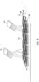
- the charging pad 402may be similar to the charging pad 130 of FIG. 1 . Further, the charging pad 402 includes the one or more first resonator coils 136 and the one or more second resonator coils 138. Particularly, the charging pad 402 includes a first layer 404 having the one or more first resonator coils 136 and a second layer 406 having the one or more second resonator coils 138. The first and second layers 404, 406 may be referred to as electrical carrier having one or more frequency coils. The first layer 404 and the second layer 406 are positioned proximate to each other in the charging pad 402.
- the first layer 404may include a plurality of first resonator coils 136 that are arranged in parallel configuration and/or serial configuration.
- the second layer 406may include a plurality of second resonator coils 138 that are arranged in parallel configuration and/or serial configuration.
- the charging pad 402may also include the excitation unit 110 that is capable of independently driving the one or more first resonator coils 136 and/or the one or more second resonator coils 138 via the corresponding exciter coils 132, 134.
- the one or more first frequency coils 116 and the one or more second frequency coils 118are stacked one above the other within the charging pad 402.
- the receiver devicesare placed at a predefined location on a top surface of the charging pad 402 in such a way that the one or more first frequency coils 116 and the one or more second frequency coils 118 are disposed below the predefined location, within the charging pad 402.
- the excitation unit 110drives the one or more first frequency coils 116 and/or the one or more second frequency coils 118 based on the frequency standard of the receiver devices.
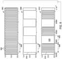
- the charging pad 502includes a single layer 504 having the one or more first resonator coils 136 and the one or more second resonator coils 138. Particularly, the first resonator coils 136 and the second resonator coils 138 are alternately positioned in the single layer 504 of the charging pad 502. In one embodiment, the one or more first resonator coils 136 and the one or more second resonator coils 138 are embedded within the charging pad 502. In one another embodiment, the first resonator coils 136 and/or the second resonator coils 138 maybe an array of coils arranged in one or more desired patterns.
- the single layer 504may be referred to as an electrical carrier having different frequency coils.
- the charging pad 402includes a first layer 404 having the one or more first resonator coils 136 and a second layer 406 having the one or more second resonator coils 138. Further, the first resonator coils 136 are magnetically coupled to the first receiver device 106 and the second resonator coils 138 are magnetically coupled to the second receiver device 108. In one embodiment, the charging pad 402 includes a surface upon which the first and second receiver devices are positioned. In another embodiment, the one of more first resonator coils 136 and the one or more second resonator coils 138 maybe positioned side-by-side on a same plane or on a different plane
- an excitation unit110receives at least one of the first frequency control signal 122 and the second frequency control signal 124 from the control unit 112. Particularly, the control unit 112 sends the first frequency control signal 122 and the second frequency control signal 124 alternately and repeatedly to the excitation unit 110.
- the power source 102supplies the input power 120 having the DC voltage to the excitation unit 110.
- the excitation unit 110converts the DC voltage of the input power 120 to the first AC voltage having a first frequency if the first frequency control signal 122 is received.
- the control unit 112sends the first frequency control signal 122 to the first switch 208 and a signal that is complimentary to the first frequency control signal 122 to the second switch 210 for the first time period.
- the first switch 208 and the second switch 210 in the excitation unit 110toggles between ON state and OFF state based on switching pulse of the first frequency control signal 122 to convert the DC voltage of the input power to the corresponding first AC voltage having the first frequency.
- the first frequencymay be in a range from about 4 MHz to about 9 MHz.
- the excitation unit 110converts the DC voltage of the input power to the second AC voltage having a second frequency if the second frequency control signal 124 is received.
- the control unit 112may send the second frequency control signal 122 to the first switch 208 and a signal that is complimentary to the first frequency control signal 122 to the second switch 210 for the second time period.
- the first switch 208 and the second switch 210 in the excitation unit 110toggles between ON state and OFF state based on switching pulse of the second frequency control signal 124 to convert the DC voltage of the input power to the corresponding second AC voltage having the second frequency.
- the second frequencymay be in a range from about 100 kHz to about 1 MHz.
- the single converter 110drives the at least one first resonator coil 136 via the at least one exciter coil 132 to transmit the first AC voltage having the frequency from the first frequency band to a first receiver device 106.
- the at least one first resonator coil 136enhances the power having the first AC voltage so that the first receiver coil 140 may receiver this power without any power loss.
- the first AC voltageis conditioned by the power conditioner 232 and supplied to the load 230 such as a battery in the first receiver device 106.
- the excitation unit 110drives the at least one second resonator coil 138 via the at least one exciter coil 134 to transmit the second AC voltage having the frequency from the second frequency band to a second receiver device 108.
- the at least one second resonator coil 138enhances the power having the second AC voltage so that the second receiver coil 142 may receiver this power without any power loss.
- the second AC voltageis conditioned by the power conditioner 234 and supplied to the load 230 such as a battery in the second receiver device 108.
- the exemplary system and methodfacilitate to charge the receiver devices of any frequency standard, using the excitation unit 110.
- Reference numeral 802is representative of a first frequency control signal transmitted from the control unit to the excitation unit for converting the DC voltage of the input power to the first AC voltage.
- the first frequency control signal 802includes a plurality of switching pulses 804 during a first time period represented by 806.
- reference numeral 808is representative of a second frequency control signal transmitted from the control unit to the excitation unit for converting the DC voltage of the input power to the second AC voltage.
- the second frequency control signal 808includes a single switching pulse 810 during a second time period represented by 820.
- the second frequency control signal 808includes more number of switching pulses within the second time period 820. However, the number of switching pulses of the second frequency control signal 808 within the second time period 820 is less than the number of switching pulses for the first frequency control signal 802 within the first time period 806.
- Reference numeral 812is representative of a modulation signal which includes the first frequency control signal 814 and the second frequency control signal 816. Particularly, the first frequency control signal 814 is generated during the first time period 806 and the second frequency control signal 816 is generated during the second time period 820.
Landscapes
- Engineering & Computer Science (AREA)
- Power Engineering (AREA)
- Computer Networks & Wireless Communication (AREA)
- Charge And Discharge Circuits For Batteries Or The Like (AREA)
Description
- Embodiments of the present invention relate generally to wireless power transfer systems and more particularly to a system and method for charging receiver devices. In general, power transfer systems are widely used to transfer power from a power source to one or more receiver devices, such as for example, mobile devices, biomedical devices, and portable consumer devices. Typically, the power transfer systems may be contact based power transfer systems or wireless power transfer systems. In certain applications, where instantaneous or continuous power transfer is required but interconnecting wires are inconvenient, the wireless power transfer systems are desirable.
- In the wireless power transfer systems, a charging device is used to convert an input power to a transferrable power which is further transmitted to charge one or batteries in the receiver devices. However, these receiver devices are compatible with one of the wireless frequency standards. For example, there are currently three competing frequency standards: the Alliance for Wireless Power (A4WP), the Wireless Power Consortium (WPC), and the Power Matters Alliance (PMA). The WPC standard (Qi) is defined in a frequency range of 100 kHz to 200 kHz. The PMA standard is defined in a frequency range of 200 kHz to 400 kHz. Further, the A4WP standard is defined at a frequency of about 7 MHz. A conventional charging device cannot be used to charge the receiver devices operating at different frequency standards. Document
US 2016/211702 A1 discloses a charging apparatus having an exciter coil which is magnetically coupled to two resonant coils. - Thus, there is a need for an improved system and method for charging receiver devices operating at different frequency standards.
- Hence the present invention, as defined by the appended claims, is provided.
- According to the present invention, a charging device according to
claim 1, and a method according to claim 10 are provided. - Various features, aspects, and advantages of the present disclosure will become better understood when the following detailed description is read with reference to the accompanying drawings in which like characters represent like parts throughout the drawings, wherein:
FIG. 1 is a block diagram representation of a wireless power transfer system in accordance with an embodiment not forming part of the present invention;FIG. 2 is a schematic representation of a wireless power transfer system in accordance with an embodiment of the present invention;FIG. 3 is a schematic representation of a wireless power transfer system in accordance with another embodiment not forming part of the present invention;FIG. 4 is a diagrammatic representation of a charging pad having first resonator and second resonator coils in accordance with an embodiment of the present invention;FIG. 5 is a diagrammatic representation of a charging pad having first resonator and second resonator coils in accordance with another embodiment of the present invention;FIG. 6 is a diagrammatic representation of a charging pad having first resonator and second resonator coils magnetically coupled to receiver devices in accordance with an embodiment of the present invention; andFIG. 7 is a flow chart illustrating a method for charging a plurality of receiver devices in accordance with an embodiment of the present invention; andFIG. 8 is a graphical representation of different control signals in accordance with an embodiment of the present invention.- As will be described in detail hereinafter, various embodiments of a system and method for charging one or more wireless receiver devices are disclosed. In particular, the system and method disclosed herein employ an excitation unit that is capable of driving first resonator and second resonator coils enabling charging of the wireless receiver devices designed based on different frequency standards.
- Unless defined otherwise, technical and scientific terms used herein have the same meaning as is commonly understood by one of ordinary skill in the art to which this specification belongs. The terms "first", "second", and the like, as used herein do not denote any order, quantity, or importance, but rather are used to distinguish one element from another. Also, the terms "a" and "an" do not denote a limitation of quantity, but rather denote the presence of at least one of the referenced items. The term "or" is meant to be inclusive and mean one, some, or all of the listed items. The use of "including," "comprising" or "having" and variations thereof herein are meant to encompass the items listed thereafter and equivalents thereof as well as additional items. The terms "connected" and "coupled" are not restricted to physical or mechanical connections or couplings, and can include electrical connections or couplings, whether direct or indirect. Furthermore, terms "circuit" and "circuitry" and "controlling unit" may include either a single component or a plurality of components, which are either active and/or passive and are connected or otherwise coupled together to provide the described function. In addition, the term operationally coupled as used herein includes wired coupling, wireless coupling, electrical coupling, magnetic coupling, radio communication, software based communication, or combinations thereof.
FIG. 1 is a diagrammatical representation of a wirelesspower transfer system 100 in accordance with an embodiment not forming part of the present invention. The wirelesspower transfer system 100 is used to transmit an electrical power from apower source 102 to one or more receiver devices such as mobile devices, biomedical devices, and portable consumer devices. Particularly, in an automobile industry, a vehicle includes one or more charging pads that are used for supplying electrical power from thepower source 102 to the mobile devices like cell phones, laptops, heating ventilation and airconditioning (HVAC) unitsetc. In one embodiment, the wirelesspower transfer system 100 may also be referred to as a contactless power transfer system.- In the illustrated embodiment, the wireless
power transfer system 100 includes awireless charging device 104 that is wirelessly coupled to afirst receiver device 106 and asecond receiver device 108. It may be noted that the wirelesspower transfer system 100 is not limited to thefirst receiver device 106 and thesecond receiver device 108 and may include any number of receiver devices. - The first and
second receiver devices first receiver device 106 is considered to be compatible with a first frequency standard such as Air Fuel Alliance standard defined at a frequency of about 6.7 MHz. The first frequency standard may also be referred to as a high frequency standard. Similarly, thesecond receiver device 108 is considered to be compatible with a second frequency standard such as WPC standard defined in a frequency range of 100 kHz to 200 kHz. The second frequency standard may also be referred to as a low frequency standard. It may be noted that thereceiver devices - In conventional power transfer systems that are compatible with different frequency standards for each of the receiver devices/gadgets, a charging device may not supply power to each of the receiver devices at their corresponding frequency standards. In one of the conventional power transfer systems, separate charging devices having a dedicated converter and dedicated frequency coils for each frequency standard, are employed to supply power to the corresponding receiver device. However, using separate charging devices for each frequency standard may substantially increase setup cost and maintenance cost of the conventional power transfer systems.
- To overcome the above problems/drawbacks associated with conventional systems, the exemplary
power transfer system 100 includes thewireless charging device 104 that is configured to charge the first andsecond receiver devices wireless charging device 104 includes acharging pad 130 and acontrol unit 112 that are used for supplying electrical power from thepower source 102 to the first andsecond receiver devices charging pad 130 may be referred to as an electrical enclosure upon which the one ormore receiver devices corresponding receiver devices control unit 112 may be positioned within thecharging pad 130. In another embodiment, thecontrol unit 112 may be positioned external to thecharging pad 130. Further, thecharging pad 130 includes an excitation unit and a transmittingunit 114. In one embodiment, theexcitation unit 110 may include one or more converters (not shown) that are used for providing electrical power at a desired frequency to the first andsecond receiver devices - The
excitation unit 110 is electrically coupled to thepower source 102 and thecontrol unit 112. Thepower source 102 is configured to supply aninput power 120 having a DC voltage to theexcitation unit 110. In some embodiments, theinput power 120 may be in a range from about 1W to 200W. In one embodiment, thepower source 102 may be a part of thewireless charging device 104. In another embodiment, thepower source 102 may be positioned external to thewireless charging device 104. - Furthermore, the
excitation unit 110 is configured to receive theinput power 120 having the DC voltage from thepower source 102. Further, theexcitation unit 110 is configured to convert the DC voltage of theinput power 120 to a first AC voltage having a frequency in a first frequency band and/or a second AC voltage having a frequency in a second frequency band. It may be noted that the first frequency band may be referred to as a range of frequencies from about 4 MHz to about 9 MHz. In a similar manner, the second frequency band may be referred to as a range of frequencies from about 100 kHz to about 1 MHz. Also, it may be noted that the terms "frequency in a first frequency band" and "first frequency" may be used interchangeably in the below specification. Similarly, the terms "frequency in a second frequency band" and "second frequency" may be used interchangeably in the below specification. - Additionally, the
excitation unit 110 is configured to receive a firstfrequency control signal 122 and/or a second frequency control signal 124 from thecontrol unit 112. If the firstfrequency control signal 122 is received from thecontrol unit 112, theexcitation unit 110 is configured to convert the DC voltage of theinput power 120 to the first AC voltage having the first frequency. In a similar manner, if the secondfrequency control signal 124 is received from thecontrol unit 112, theexcitation unit 110 is configured to convert the DC voltage of theinput power 120 to the second AC voltage having the second frequency. In one example, the first and second AC voltages may be in a range from about 5 volts to 50 volts. The details pertaining to converting the DC voltage to the first AC voltage or the second AC voltage are explained in greater detail below with reference toFIGS. 2 and3 . - In one embodiment, the
control unit 112 is configured to alternately send the firstfrequency control signal 122 and the secondfrequency control signal 124 at regular time intervals to theexcitation unit 110. In one specific embodiment, thecontrol unit 112 is configured to send a modulation signal including the firstfrequency control signal 122 and the secondfrequency control signal 124. In another embodiment, thecontrol unit 112 is configured to concurrently send the firstfrequency control signal 122 and the secondfrequency control signal 124 to different sets of switches in theexcitation unit 110. - The
excitation unit 110 is further configured to transmit the input power having the first AC voltage or the second AC voltage to the transmittingunit 114. The transmittingunit 114 includes one or more exciter coils 132, 134 that are electrically coupled to theexcitation unit 110. In addition to the exciter coils 132, 134, the transmittingunit 114 includes one or more first resonator coils 136 and one or more second resonator coils 138. The one or more first resonator coils 136 are magnetically coupled to theexciter coil 132 and afirst receiver coil 140 in thefirst receiver device 106. Similarly, the one or more second resonator coils 138 are magnetically coupled to theexciter coil 134 and asecond receiver coil 142 in thesecond receiver device 108. In one embodiment, the one or more first resonator coils 136 and the one or more second resonator coils 138 may be stacked one above the other. Further, a single exciter coil may be used to drive the one or more first resonator coils 136 and/or the one or more second resonator coils 138. In another embodiment, the one or more first resonator coils 136 and the one or more second resonator coils 138 may be positioned side-by-side on a same plane or on a different plane. - Further, the exciter coils 132, 134 and the one or more first and second resonator coils 136, 138 are used to wirelessly transmit the input power having the first AC voltage or the second AC voltage to the
receiver devices excitation unit 110 converts the DC voltage to the first AC voltage having the first frequency, theexciter coil 132 and the one or more first resonator coils 136 are excited simultaneously to transmit the input power having the first AC voltage to thefirst receiver coil 140 of thefirst receiver device 106. In a similar manner, if theexcitation unit 110 converts the DC voltage to the second AC voltage having the second frequency, theexciter coil 134 and the one or more second resonator coils 138 are excited simultaneously to transmit the input power having the second AC voltage to thesecond receiver coil 142 of thesecond receiver device 108. Advantageously, the resonator coils 136, 138 in thecharging device 104 facilitates in transmitting the power to a longer distance between thereceiver devices wireless charging device 104. In one embodiment, a distance between thereceiver devices wireless charging device 104 may be in a range from about 10 mm to about 100 mm. - Further, the first and
second receiver devices more batteries second receiver devices second receiver devices second receiver devices first receiver device 106 is designed to the first frequency standard such as Air Fuel Alliance standard, thefirst receiver device 106 receives the first AC voltage having the first frequency from the first resonator coils 136. Similarly, if thesecond receiver device 108 is designed to a second frequency standard such as WPC standard, thesecond receiver device 108 receives the second AC voltage having the second frequency from the second resonator coils 138. In one example, the first andsecond receiver devices charging pad 130 for charging thebatteries second receiver devices - Thus, by employing the exemplary wireless
power transfer system 100, thesingle charging device 104 is configured to magnetically transfer power to the first andsecond receiver devices - Referring to
FIG. 2 , a schematic representation of the wirelesspower transfer system 100 in accordance with another embodiment of the present invention is depicted. The wirelesspower transfer system 100 is used to transmit theinput power 120 from thepower source 102 to the first andsecond receiver devices - The wireless
power transfer system 100 includes thewireless charging device 104, thefirst receiver device 106, and thesecond receiver device 108. Thewireless charging device 104 is wirelessly coupled to thefirst receiver device 106 and thesecond receiver device 108. Thefirst receiver device 106 and thesecond receiver device 108 may be compatible with one of the wireless frequency standards. - Further, the
wireless charging device 104 includes thecharging pad 130 and thecontrol unit 112 that are used for supplying electrical power from thepower source 102 to the first andsecond receiver devices charging pad 130 includes theexcitation unit 110 and the transmittingunit 114. It may be noted that the wirelesspower transfer system 100 may include other components and is not be limited to the components shown inFIG. 2 . - In the illustrated embodiment, the
excitation unit 110 includes only asingle converter 216 that is electrically coupled to thepower source 102 and configured to receive theinput power 120 having the DC voltage from thepower source 102. Thesingle converter 216 is defined as an electrically connected device that has single DC or line frequency input. It may be noted that theexcitation unit 110 may include any number of converters, and is not limited to a single converter as depicted inFIG. 2 . Further, thesingle converter 216 includes afirst switch 208, asecond switch 210, a plurality ofdiodes 212, and a plurality ofcapacitors 214 that are arranged to form a half bridge inverter circuit. The first andsecond switches diodes 212, and thecapacitors 214 are electrically coupled betweeninput terminals 217 andoutput terminals 218 of theexcitation unit 110. In one embodiment, theswitches switches first switch 208 and thesecond switch 210 are operated complimentary to each other. For example, if thefirst switch 208 is activated for a time duration Ton, thesecond switch 210 is deactivated for this time duration Ton. Similarly, if thesecond switch 210 is activated for the time duration Toff, thefirst switch 208 is deactivated for this time duration Toff. - Furthermore, the
control unit 112 is configured to alternately and repeatedly send a firstfrequency control signal 122 and a secondfrequency control signal 124 to thefirst switch 208 and thesecond switch 210. In one embodiment, thecontrol unit 112 may generate the first and second frequency control signals 122, 124 based on change in characteristics of anexciter coil 202. For example, if thefirst receiver device 106 and/or thesecond receiver device 108 are placed on thecharging pad 130, the characteristics such as electrical current in theexciter coil 202 may change. Further, the change in the characteristics of theexciter coil 202 may be used by thecontrol unit 112 to generate the first and second frequency control signals 122, 124. - Furthermore, the
control unit 112 sends the firstfrequency control signal 122 to thefirst switch 208 for a first time period. Concurrently, thecontrol unit 112 sends a signal that is complimentary to the firstfrequency control signal 122 to thesecond switch 210 for the first time period. In one example, the firstfrequency control signal 122 may have a high switching pulse frequency of about 7 MHz. During the first time period, thefirst switch 208 and thesecond switch 210 are operated complimentary to each other to convert the DC voltage of theinput power 120 to the first AC voltage having a first frequency. In one embodiment, the first frequency may be in a range from about 4 MHz to about 9 MHz. In one specific embodiment, thefirst switch 208 and thesecond switch 210 are configured to modulate the DC voltage of theinput power 120 based on the firstfrequency control signal 122 to generate the first AC voltage having the first frequency at theoutput terminals 218 of theexcitation unit 110. - In a similar manner, the
control unit 112 sends the secondfrequency control signal 124 to thefirst switch 208 for a second time period. Concurrently, thecontrol unit 112 sends a signal that is complimentary to the second frequency control signal to thesecond switch 210 for the second time period. In one embodiment, the secondfrequency control signal 124 may have a low switching pulse frequency of about 200 kHz. During the second time period, thefirst switch 208 and thesecond switch 210 are operated complimentary to each other to convert the DC voltage of theinput power 120 to the second AC voltage having a second frequency. In one embodiment, the second frequency may be in a range from about 100 kHz to about 1 MHz. In one embodiment, thefirst switch 208 and thesecond switch 210 are configured to modulate the DC voltage of theinput power 120 based on the secondfrequency control signal 124 to provide the second AC voltage having the second frequency at theoutput terminals 218 of theexcitation unit 110. - Further, the input power having the first AC voltage or the second AC voltage is transmitted from the
excitation unit 110 to the transmittingunit 114. The transmittingunit 114 includes anexciter coil 202 that is electrically coupled to theoutput terminals 218 of theexcitation unit 110. It may be noted that theexciter coil 202 may be similar to one of the exciter coils 132, 134 shown inFIG. 1 . Further, the transmittingunit 114 includes the one or more first resonator coils 136 and one or more second resonator coils 138. For ease of illustration, only onefirst resonator coil 136 and onesecond resonator coil 138 are shown. Thefirst resonator coil 136 is magnetically coupled to theexciter coil 202 and thefirst receiver coil 140 in thefirst receiver device 106. Thefirst resonator coil 136 and theexciter coil 202 are used to transfer the power having the first AC voltage to thefirst receiver coil 140 in thefirst receiver device 106. Further, the power having the first AC voltage is then transmitted from thefirst receiver coil 140 to anelectric load 228 such as a battery in thefirst receiver device 106 via apower conditioner 232. - In a similar manner, the
second resonator coil 138 is magnetically coupled to theexciter coil 202 and thesecond receiver coil 142 in thesecond receiver device 108. Thesecond resonator coil 138 and theexciter coil 202 are used to transfer the power having the second AC voltage to thesecond receiver coil 142 in thesecond receiver device 108. Further, the power having the second AC voltage is then transmitted from thesecond receiver coil 142 to anelectric load 230 such as a battery in thesecond receiver device 108 via apower conditioner 234. In another embodiment, the transmittingunit 112 may include two exciter coils, where one exciter coil is magnetically coupled to the first resonator coils 136, while the other exciter coil is magnetically coupled to the second resonator coils 138. - During normal operation of the wireless
power transfer system 100, thecontrol unit 112 is configured to periodically and/or alternately send the firstfrequency control signal 122 and the secondfrequency control signal 124 to theexcitation unit 110. Particularly, thecontrol unit 112 sends the firstfrequency control signal 122 to thefirst switch 208 and a signal that is complimentary to the firstfrequency control signal 122 to thesecond switch 210 for the first time period. Further, during the first time period, thefirst switch 208 and thesecond switch 210 toggles between ON state and OFF state based on switching pulse of the firstfrequency control signal 122 to convert the DC voltage of the input power to the corresponding first AC voltage having the first frequency. It may be noted that the ON state may be referred to as a state where theswitches switches - Further, the input power having the first AC voltage may be used to excite the
exciter coil 202 and thefirst resonator coil 136 simultaneously. Particularly, theexciter coil 202 may generate a magnetic field that is corresponding to the first AC voltage. Further, the generated magnetic field may be focused towards thefirst receiver coil 140 via thefirst resonator coil 136. In one embodiment, thefirst resonator coil 136 and one or more capacitors may be used to enhance the magnetic field generated by theexciter coil 202. Subsequently, thefirst receiver coil 140 is configured to receive the enhanced magnetic field and convert the enhanced magnetic field to the input power having the first AC voltage. In one embodiment, thefirst resonator coil 136 is used to enhance the magnetic coupling between theexciter coil 202 and thefirst receiver coil 140. Thefirst receiver coil 140 transmits the first AC voltage having the first frequency to theelectric load 228 via thepower conditioner 232. - Furthermore, at the end of the first time period, the
control unit 112 sends the secondfrequency control signal 122 to thefirst switch 208 and a signal that is complimentary to the firstfrequency control signal 122 to thesecond switch 210 for the second time period. Further, during the second time period, thefirst switch 208 and thesecond switch 210 toggles between ON state and OFF state based on switching pulse of the secondfrequency control signal 124 to convert the DC voltage of the input power to the corresponding second AC voltage having the second frequency. - Further, the input power having the
second AC voltage 110 may be used to excite theexciter coil 202 and thesecond resonator coil 138 simultaneously. Particularly, theexciter coil 202 may generate a magnetic field that is corresponding to the second AC voltage. Further, the generated magnetic field may be focused towards thesecond receiver coil 142 via thesecond resonator coil 138. In one embodiment, thesecond resonator coil 138 and one or more capacitors may be used to enhance the magnetic field generated by theexciter coil 202. Subsequently, thesecond receiver coil 142 is configured to receive the enhanced magnetic field and convert the enhanced magnetic field to the input power having the second AC voltage. In one embodiment, thesecond resonator coil 138 is used to enhance the magnetic coupling between theexciter coil 202 and thesecond receiver coil 142. Thereafter, thesecond receiver coil 142 transmits the second AC voltage having the second frequency to theelectric load 230 via thepower conditioner 234. In one embodiment, thecontrol unit 112 alternately sends the firstfrequency control signal 122 and the secondfrequency control signal 124 to theexcitation unit 110 to transmit the first AC voltage having the first frequency and the second AC voltage having the second frequency to the correspondingreceiver devices - In the exemplary
power transfer system 100, theexcitation unit 110 drives both thefirst resonator coil 136 and thesecond resonator coil 138 to transfer the power from thepower source 102 to thereceiver devices FIG. 3 , a schematic representation of a wirelesspower transfer system 300 in accordance with another embodiment not forming part of the present invention is depicted. The wirelesspower transfer system 300 ofFIG. 3 is similar to the wirelesspower transfer system 100 ofFIG. 2 except that theexcitation unit 302 includes a single converter 304 having a full bridge inverter circuit and the transmittingunit 114 includes afirst exciter coil 310 and asecond exciter 312. Particularly, the single converter 304 includes a first leg ofswitches 306 and a second leg ofswitches 308. The first leg ofswitches 306 is configured to receive a first frequency control signal 122 from thecontrol unit 112 and the second leg ofswitches 308 is configured to receive a second frequency control signal 124 from thecontrol unit 112. In this embodiment, the firstfrequency control signal 122 is a continuous signal having a high switching pulse frequency of about 6.7 MHz and the secondfrequency control signal 124 is a continuous signal having a low switching pulse frequency of about 200 kHz. - The first leg of
switches 306 is activated if the firstfrequency control signal 122 is received. Further, the first leg ofswitches 306 is configured to convert a DC voltage of theinput power 120 to a first AC voltage having a first frequency. In one embodiment, this first frequency may be in a range from about 4 MHz to about 9 MHz. The first AC voltage having the first frequency is transmitted to thefirst exciter coil 310, which in turn magnetically transfers the power having the first AC voltage to thefirst receiver device 106 via thefirst resonator coil 136. In one embodiment, thefirst resonator coil 136 enhances the power having the first AC voltage so that thefirst receiver device 106 may receive the power without or negligible power loss. - In a similar manner, the second leg of
switches 308 is activated if the secondfrequency control signal 124 is received. Further, the second leg ofswitches 308 is configured to convert the DC voltage of theinput power 120 to a second AC voltage having a second frequency. In one embodiment, the second frequency may be in a range from about 100 kHz to about 1 MHz. The second AC voltage having the second frequency is transmitted to thesecond exciter coil 312, which in turn magnetically transfers the power having the second AC voltage to thesecond receiver device 108 via thesecond resonator coil 138. In one embodiment, thesecond resonator coil 138 enhances the power having the second AC voltage so that thesecond receiver device 108 may receive this power without or negligible power loss. - Referring to
FIG. 4 , a schematic representation of acharging pad 402 in accordance with an exemplary embodiment is depicted. Thecharging pad 402 may be similar to thecharging pad 130 ofFIG. 1 . Further, thecharging pad 402 includes the one or more first resonator coils 136 and the one or more second resonator coils 138. Particularly, thecharging pad 402 includes afirst layer 404 having the one or more first resonator coils 136 and asecond layer 406 having the one or more second resonator coils 138. The first andsecond layers first layer 404 and thesecond layer 406 are positioned proximate to each other in thecharging pad 402. In one embodiment, thefirst layer 404 may include a plurality of first resonator coils 136 that are arranged in parallel configuration and/or serial configuration. Similarly, thesecond layer 406 may include a plurality of second resonator coils 138 that are arranged in parallel configuration and/or serial configuration. In one another embodiment, thecharging pad 402 may also include theexcitation unit 110 that is capable of independently driving the one or more first resonator coils 136 and/or the one or more second resonator coils 138 via the corresponding exciter coils 132, 134. - The one or more first frequency coils 116 and the one or more second frequency coils 118 are stacked one above the other within the
charging pad 402. The receiver devices are placed at a predefined location on a top surface of thecharging pad 402 in such a way that the one or more first frequency coils 116 and the one or more second frequency coils 118 are disposed below the predefined location, within thecharging pad 402. Theexcitation unit 110 drives the one or more first frequency coils 116 and/or the one or more second frequency coils 118 based on the frequency standard of the receiver devices. - Referring to
FIG. 5 , a schematic representation of acharging pad 502 in accordance with another embodiment is depicted. Thecharging pad 502 includes asingle layer 504 having the one or more first resonator coils 136 and the one or more second resonator coils 138. Particularly, the first resonator coils 136 and the second resonator coils 138 are alternately positioned in thesingle layer 504 of thecharging pad 502. In one embodiment, the one or more first resonator coils 136 and the one or more second resonator coils 138 are embedded within thecharging pad 502. In one another embodiment, the first resonator coils 136 and/or the second resonator coils 138 maybe an array of coils arranged in one or more desired patterns. Thesingle layer 504 may be referred to as an electrical carrier having different frequency coils. - Referring to
FIG. 6 , a schematic representation of thecharging pad 402 in accordance with an exemplary embodiment is depicted. Thecharging pad 402 includes afirst layer 404 having the one or more first resonator coils 136 and asecond layer 406 having the one or more second resonator coils 138. Further, the first resonator coils 136 are magnetically coupled to thefirst receiver device 106 and the second resonator coils 138 are magnetically coupled to thesecond receiver device 108. In one embodiment, thecharging pad 402 includes a surface upon which the first and second receiver devices are positioned. In another embodiment, the one of more first resonator coils 136 and the one or more second resonator coils 138 maybe positioned side-by-side on a same plane or on a different plane - Referring to
FIG. 7 , a flow chart illustrating a method for charging a plurality of receiver devices in accordance with an embodiment of the present invention is depicted. Themethod 700 is described with reference toFIGs. 1 and2 . Atstep 702, an excitation unit110 receives at least one of the firstfrequency control signal 122 and the second frequency control signal 124 from thecontrol unit 112. Particularly, thecontrol unit 112 sends the firstfrequency control signal 122 and the secondfrequency control signal 124 alternately and repeatedly to theexcitation unit 110. Thepower source 102 supplies theinput power 120 having the DC voltage to theexcitation unit 110. - Subsequently, at
step 704, theexcitation unit 110 converts the DC voltage of theinput power 120 to the first AC voltage having a first frequency if the firstfrequency control signal 122 is received. Particularly, thecontrol unit 112 sends the firstfrequency control signal 122 to thefirst switch 208 and a signal that is complimentary to the firstfrequency control signal 122 to thesecond switch 210 for the first time period. Further, during this first time period, thefirst switch 208 and thesecond switch 210 in theexcitation unit 110 toggles between ON state and OFF state based on switching pulse of the firstfrequency control signal 122 to convert the DC voltage of the input power to the corresponding first AC voltage having the first frequency. In one embodiment, the first frequency may be in a range from about 4 MHz to about 9 MHz. - Furthermore, at
step 706, theexcitation unit 110 converts the DC voltage of the input power to the second AC voltage having a second frequency if the secondfrequency control signal 124 is received. Particularly, thecontrol unit 112 may send the secondfrequency control signal 122 to thefirst switch 208 and a signal that is complimentary to the firstfrequency control signal 122 to thesecond switch 210 for the second time period. Further, during this second time period, thefirst switch 208 and thesecond switch 210 in theexcitation unit 110 toggles between ON state and OFF state based on switching pulse of the secondfrequency control signal 124 to convert the DC voltage of the input power to the corresponding second AC voltage having the second frequency. In one embodiment, the second frequency may be in a range from about 100 kHz to about 1 MHz. - At
step 708, thesingle converter 110 drives the at least onefirst resonator coil 136 via the at least oneexciter coil 132 to transmit the first AC voltage having the frequency from the first frequency band to afirst receiver device 106. Particularly, the at least onefirst resonator coil 136 enhances the power having the first AC voltage so that thefirst receiver coil 140 may receiver this power without any power loss. Further, the first AC voltage is conditioned by thepower conditioner 232 and supplied to theload 230 such as a battery in thefirst receiver device 106. - Furthermore, at
step 710, theexcitation unit 110 drives the at least onesecond resonator coil 138 via the at least oneexciter coil 134 to transmit the second AC voltage having the frequency from the second frequency band to asecond receiver device 108. Particularly, the at least onesecond resonator coil 138 enhances the power having the second AC voltage so that thesecond receiver coil 142 may receiver this power without any power loss. Further, the second AC voltage is conditioned by thepower conditioner 234 and supplied to theload 230 such as a battery in thesecond receiver device 108. - In accordance with the exemplary embodiments discussed herein, the exemplary system and method facilitate to charge the receiver devices of any frequency standard, using the
excitation unit 110. - Referring to
FIG. 8 , a graphical representation of different control signals in accordance with aspects of the present invention is shown.Reference numeral 802 is representative of a first frequency control signal transmitted from the control unit to the excitation unit for converting the DC voltage of the input power to the first AC voltage. The firstfrequency control signal 802 includes a plurality of switchingpulses 804 during a first time period represented by 806. Further,reference numeral 808 is representative of a second frequency control signal transmitted from the control unit to the excitation unit for converting the DC voltage of the input power to the second AC voltage. The secondfrequency control signal 808 includes asingle switching pulse 810 during a second time period represented by 820. It should be noted herein that the secondfrequency control signal 808 includes more number of switching pulses within thesecond time period 820. However, the number of switching pulses of the secondfrequency control signal 808 within thesecond time period 820 is less than the number of switching pulses for the firstfrequency control signal 802 within thefirst time period 806.Reference numeral 812 is representative of a modulation signal which includes the firstfrequency control signal 814 and the secondfrequency control signal 816. Particularly, the firstfrequency control signal 814 is generated during thefirst time period 806 and the secondfrequency control signal 816 is generated during thesecond time period 820. - While only certain features of the present disclosure have been illustrated and described herein, many modifications and changes will occur to those skilled in the art. It io,
Claims (14)
- A wireless charging device (104), comprising:a charging pad (130, 402, 502) that comprises:a first resonator coil (136) operable at a first frequency band;a second resonator coil (138) operable at a second frequency band;an exciter coil (202) magnetically coupled to both the first resonator coil (136) and the second resonator coil (138), wherein the exciter coil (202) is operable to provide a first AC voltage to the first resonator coil (136) at a first frequency within the first frequency band, and to provide a second AC voltage to the second resonator coil (138) at a second frequency within the second frequency band; andan excitation unit (110) that comprises output terminals electrically coupled to the exciter coil (202) and configured to drive the first resonator coil (136) with the first AC voltage at the first frequency and the second resonator coil (138) with the second AC voltage at the second frequency via the exciter coil (202); anda control unit (112) that is configured to generate a first frequency control signal (122) and a second frequency control signal (124) to feed at least one of the first frequency control signal (122) and the second frequency control signal (124) to the excitation unit (110) so as to selectively cause the first resonator coil (136) to be driven with the first AC voltage or the second resonator coil (138) to be driven with the second AC voltage by the excitation unit (110).
- The wireless charging device (104) of claim 1, wherein the excitation unit (110) is further configured to:receive at least one of the first frequency control signal (122) and the second frequency control signal (124) from the control unit (112);convert a DC voltage of an input power (120) to the first AC voltage having a frequency from the first frequency band if the first frequency control signal (122) is received; andconvert the DC voltage of the input power (120) to the second AC voltage having a frequency from the second frequency band if the second frequency control signal (124) is received.
- The wireless charging device (104) of any preceding claim, wherein the excitation unit (110, 302) is configured to drive the first resonator coil (136) via the exciter coil ( 202) to transfer the first AC voltage having the frequency from the first frequency band to a first receiver device (106).
- The wireless charging device (104) of any preceding claim, wherein the excitation unit (110, 302) is configured to drive the second resonator coil (138) via the exciter coil ( 202) to transfer the second AC voltage having the frequency from the second frequency band to a second receiver device (108).
- The wireless charging device (104) of any preceding claim, further comprising:a first layer (404) comprising the first resonator coil (136); anda second layer (406) comprising the second resonator coil (138).
- The wireless charging device (104) of any preceding claim, further comprising a single layer (504) comprising the first resonator coil (136) and the second resonator coil (138).
- The wireless charging device (104) of any preceding claim, wherein the excitation unit (110, 302) comprises only a single converter (216, 304) that is configured to drive the first resonator coil (136) and the second resonator coil (138) via the exciter coil (132, 134, 202, 310, 312).
- The wireless charging device (104) of any preceding claim, wherein the first resonator coil (136) and the second resonator coil (138) are stacked one above the other.
- The wireless charging device (104) of any preceding claim, wherein the control unit (112) is configured to feed a modulation signal (812) comprising at least one of the first frequency control signal (122, 814) and the second frequency control signal (124, 816).
- A wireless charging method comprisingreceiving, by an excitation unit (110), at least one of a first frequency control signal (122) and a second frequency control signal (124) from a control unit (112);converting, by the excitation unit (110), a DC voltage of an input power (120) to a first AC voltage at a first frequency within a first frequency band if the first frequency control signal (122) is received;converting, by the excitation unit (110, 302), the DC voltage of the input power (120) to a second AC voltage at a second frequency from a second frequency band if the second frequency control signal (124) is received;outputting, via output terminals of the excitation unit (110), the first AC voltage at the first frequency or the second AC voltage at the second frequency to an exciter coil (202) of a transmitting unit (114) that comprises a first resonator coil (136) and a second resonator coil (138), wherein the exciter coil (202) is magnetically coupled to both the first and second resonator coils;thereby selectively driving the first resonator coil (136) via the exciter coil (202) to transmit the first AC voltage at the first frequency within the first frequency band to a first receiver device (106); orselectively driving the second resonator coil (138) via the exciter coil (202) to transmit the second AC voltage at the second frequency within the second frequency band to a second receiver device (108).
- The method of claim 10, further comprising:sending, by the control unit (112), at least one of the first frequency control signal (122) and the second frequency control signal (124) to the excitation unit (110); andsupplying, by a power source (102), the input power (120) having the DC voltage to the excitation unit (110).
- The method of claim 10 or claim 11, further comprising:driving, by the excitation unit (110), the first resonator coil (136) via the exciter coil (202) if the first frequency control signal (122) is received from the control unit (112); anddriving, by the excitation unit (110), the second resonator coil (138) via the exciter coil (202) if the second frequency control signal (124) is received from the control unit (112).
- The method of any of claims 10 to 12, further comprising receiving, by the first receiver device (106), the first AC voltage at the first frequency within the first frequency band, to charge at least one battery (126) in the first receiver device (106).
- The method of any of claims 10 to 13, further comprising receiving, by the second receiver device (108), the second AC voltage at the second frequency within the second frequency band, to charge at least one battery (128) in the second receiver device(108).
Applications Claiming Priority (1)
| Application Number | Priority Date | Filing Date | Title |
|---|---|---|---|
| IN201641026650 | 2016-08-04 |
Publications (2)
| Publication Number | Publication Date |
|---|---|
| EP3280030A1 EP3280030A1 (en) | 2018-02-07 |
| EP3280030B1true EP3280030B1 (en) | 2023-08-30 |
Family
ID=59362983
Family Applications (1)
| Application Number | Title | Priority Date | Filing Date |
|---|---|---|---|
| EP17181476.7AActiveEP3280030B1 (en) | 2016-08-04 | 2017-07-14 | System and method for charging receiver devices |
Country Status (4)
| Country | Link |
|---|---|
| US (1) | US10897153B2 (en) |
| EP (1) | EP3280030B1 (en) |
| JP (2) | JP7330662B2 (en) |
| CN (2) | CN107689649B (en) |
Families Citing this family (14)
| Publication number | Priority date | Publication date | Assignee | Title |
|---|---|---|---|---|
| SG10201705912TA (en)* | 2016-08-04 | 2018-03-28 | Gen Electric | System and method for charging receiver devices |
| WO2018190985A1 (en)* | 2017-04-14 | 2018-10-18 | General Electric Company | A wireless power transceiver device and an associated method thereof |
| WO2019177357A1 (en)* | 2018-03-14 | 2019-09-19 | 주식회사 아모센스 | Wireless power receiving module and portable electronic device comprising same |
| KR102574119B1 (en) | 2018-07-03 | 2023-09-05 | 삼성전자주식회사 | Electronic device and method for controlling multi wireless transmitting power based on states of a plurality of external electronic devices |
| CN109104000B (en)* | 2018-10-10 | 2021-07-30 | 上海交通大学 | Single-input multiple-output control system and method based on magnetic coupling resonance |
| US11303145B2 (en)* | 2018-12-11 | 2022-04-12 | Denso Corporation | Charging system |
| KR102241145B1 (en)* | 2019-10-24 | 2021-04-19 | 서울시립대학교 산학협력단 | On-line wireless power transfer system and wireless power transmission coil thereof |
| CN111342567A (en)* | 2020-03-28 | 2020-06-26 | 华中科技大学 | A dual-frequency omnidirectional wireless power transmission system |
| US11764617B2 (en) | 2021-02-10 | 2023-09-19 | Nucurrent, Inc. | Wireless power receivers for virtual AC power signals |
| US11923695B2 (en)* | 2021-02-10 | 2024-03-05 | Nucurrent, Inc. | Wireless power transmitters for virtual AC power signals |
| US11289952B1 (en) | 2021-02-10 | 2022-03-29 | Nucurrent, Inc. | Slotted communications in virtual AC power signal transfer with variable slot width |
| US11942797B2 (en) | 2021-02-10 | 2024-03-26 | Nucurrent, Inc. | Virtual AC power signal transfer using wireless power transfer system |
| US11444492B2 (en) | 2021-02-10 | 2022-09-13 | Nucurrent, Inc. | Wireless power transfer systems for kitchen appliances |
| US11791663B2 (en)* | 2021-02-10 | 2023-10-17 | Nucurrent, Inc. | Slotted communications in virtual AC power signal transfer |
Citations (1)
| Publication number | Priority date | Publication date | Assignee | Title |
|---|---|---|---|---|
| US20100187913A1 (en)* | 2008-08-20 | 2010-07-29 | Smith Joshua R | Wireless power transfer apparatus and method thereof |
Family Cites Families (54)
| Publication number | Priority date | Publication date | Assignee | Title |
|---|---|---|---|---|
| US3950691A (en)* | 1973-09-28 | 1976-04-13 | Shunjiro Ohba | High-output solid state dc-ac inverter with improved overload protection and control logic circuitry |
| GB0124887D0 (en)* | 2001-10-17 | 2001-12-05 | Qinetiq Ltd | Metal detection apparatus |
| CA2360652C (en)* | 2001-10-31 | 2005-08-02 | Global Thermoelectric Inc. | Transformerless two phase inverter |
| KR100564256B1 (en) | 2004-06-25 | 2006-03-29 | 주식회사 한림포스텍 | Wireless charging pads and battery packs with radio frequency identification technology |
| US7221107B2 (en)* | 2005-04-13 | 2007-05-22 | Ballastronic, Inc. | Low frequency electronic ballast for gas discharge lamps |
| US7952322B2 (en) | 2006-01-31 | 2011-05-31 | Mojo Mobility, Inc. | Inductive power source and charging system |
| US8169185B2 (en) | 2006-01-31 | 2012-05-01 | Mojo Mobility, Inc. | System and method for inductive charging of portable devices |
| EP2082468A2 (en)* | 2006-10-26 | 2009-07-29 | Koninklijke Philips Electronics N.V. | Floor covering and inductive power system |
| WO2009069844A1 (en) | 2007-11-30 | 2009-06-04 | Chun-Kil Jung | Multiple non-contact charging system of wireless power transmision and control method thereof |
| US9124113B2 (en) | 2008-07-07 | 2015-09-01 | Powerbyproxi Limited | Inductively coupled power receiver and method of operation |
| US20110074346A1 (en)* | 2009-09-25 | 2011-03-31 | Hall Katherine L | Vehicle charger safety system and method |
| AU2010234396A1 (en)* | 2009-04-08 | 2011-10-27 | Access Business Group International Llc | Selectable coil array |
| US8138688B2 (en) | 2010-01-22 | 2012-03-20 | Averd Labs Co., Ltd. | Half-bridge power converter for driving LED by series-resonant connection of inductor, inductor and capacitor |
| JP5691458B2 (en)* | 2010-03-31 | 2015-04-01 | 日産自動車株式会社 | Non-contact power feeding apparatus and non-contact power feeding method |
| JP5605153B2 (en)* | 2010-10-15 | 2014-10-15 | ソニー株式会社 | Power supply device, power supply method, and power supply system |
| CN103262660A (en)* | 2010-12-02 | 2013-08-21 | 株式会社日立医疗器械 | Anode rotational drive device and X-ay imaging device |
| KR101171937B1 (en) | 2010-12-30 | 2012-08-07 | 전자부품연구원 | Multi-node wireless power transmission system and wirelss chargeable device using magnetic resonance induction |
| JP5058350B1 (en)* | 2011-03-30 | 2012-10-24 | 株式会社東芝 | Power transmission device and power transmission system |
| JP5781392B2 (en) | 2011-07-28 | 2015-09-24 | 三洋電機株式会社 | Battery pack, battery driving device, and contactless charging method of battery pack |
| CA2788895C (en)* | 2011-09-07 | 2020-08-18 | Solace Power Inc. | Wireless electric field power transmission system and method |
| US9079043B2 (en)* | 2011-11-21 | 2015-07-14 | Thoratec Corporation | Transcutaneous power transmission utilizing non-planar resonators |
| RU2596613C2 (en)* | 2012-02-22 | 2016-09-10 | Тойота Дзидося Кабусики Кайся | Contactless power transmission, power receiving device and system for contactless power transmission |
| JP5868490B2 (en)* | 2012-03-30 | 2016-02-24 | 株式会社日立製作所 | Insulated transmission medium and insulated transmission device |
| US9343922B2 (en)* | 2012-06-27 | 2016-05-17 | Witricity Corporation | Wireless energy transfer for rechargeable batteries |
| US9143000B2 (en) | 2012-07-06 | 2015-09-22 | Energous Corporation | Portable wireless charging pad |
| FR2993418B1 (en)* | 2012-07-13 | 2014-07-18 | Continental Automotive France | DEVICE FOR CHARGING A PORTABLE MEMBER AND ASSOCIATED METHOD |
| US10658869B2 (en)* | 2012-08-03 | 2020-05-19 | Mediatek Inc. | Multi-mode, multi-standard wireless power transmitter coil assembly |
| KR102096560B1 (en)* | 2012-09-11 | 2020-04-03 | 필립스 아이피 벤쳐스 비.브이. | Wireless power control |
| CN104052161B (en)* | 2013-03-12 | 2018-10-19 | 海尔集团公司 | Adapt to the radio energy transmission system of multi-load switching at runtime |
| US9643505B2 (en)* | 2013-04-26 | 2017-05-09 | Toyota Jidosha Kabushiki Kaisha | Power receiving device, power transmitting device, power transfer system, and parking assisting device |
| JP6092017B2 (en)* | 2013-06-25 | 2017-03-08 | ルネサスエレクトロニクス株式会社 | Power transmission device, non-contact power feeding system, and control method |
| EP3032699B1 (en)* | 2013-07-31 | 2018-10-10 | Panasonic Corporation | Wireless electricity transmission device and wireless power transmission system |
| US10122212B2 (en)* | 2013-08-30 | 2018-11-06 | Samsung Electro-Mechanics Co., Ltd. | Power supply device |
| US10186912B2 (en) | 2013-09-13 | 2019-01-22 | Qualcomm Incorporated | Pickup coil design for tight spaces and asymmetrical coupling |
| JP6165009B2 (en)* | 2013-09-27 | 2017-07-19 | エスアイアイ・セミコンダクタ株式会社 | Power supply system, power supply apparatus, and power supply method |
| JP6258816B2 (en)* | 2013-10-29 | 2018-01-10 | パナソニック株式会社 | Wireless power transmission apparatus and wireless power transmission system |
| JP5904250B2 (en) | 2013-11-28 | 2016-04-13 | Tdk株式会社 | Coil unit and non-contact power transmission device |
| KR20160067217A (en) | 2013-12-02 | 2016-06-13 | 후지쯔 가부시끼가이샤 | Power reception apparatus, power transmission apparatus, and wireless power supply system |
| US9153998B2 (en) | 2013-12-02 | 2015-10-06 | Qualcomm Incorporated | Wireless power orthogonal polarization antenna array |
| JP6315382B2 (en)* | 2013-12-19 | 2018-04-25 | パナソニックIpマネジメント株式会社 | Power transmission device, power reception device, and wireless power transmission system for wireless power transmission |
| TW201531831A (en)* | 2014-02-11 | 2015-08-16 | Hon Hai Prec Ind Co Ltd | On-vehicle wireless charger |
| CN105594098B (en)* | 2014-02-28 | 2020-01-21 | 松下知识产权经营株式会社 | Foreign object detection device, power transmission device and power reception device for wireless power transmission, and wireless power transmission system |
| EP2928038A1 (en)* | 2014-03-31 | 2015-10-07 | ABB Technology AG | Inductive power transfer system and method for operating an inductive power transfer system |
| US9837830B2 (en)* | 2014-04-25 | 2017-12-05 | Electronics And Telecommunications Research Institute | Wireless power transmitting method and apparatus using dual-loop in-phase feeding |
| US10135303B2 (en) | 2014-05-19 | 2018-11-20 | Apple Inc. | Operating a wireless power transfer system at multiple frequencies |
| CN105226843B (en)* | 2014-05-27 | 2017-09-15 | 松下知识产权经营株式会社 | Wireless power transmission system and power transmission device of wireless power transmission system |
| JP6269375B2 (en)* | 2014-07-30 | 2018-01-31 | 船井電機株式会社 | Non-contact power supply device and non-contact power supply system |
| EP3204999A4 (en)* | 2014-10-06 | 2018-06-13 | Robert Bosch GmbH | Wireless charging system for devices in a vehicle |
| CN204167945U (en)* | 2014-10-14 | 2015-02-18 | 深圳市友利来电源科技有限公司 | One prevents self discharge wireless charging device |
| US10128663B2 (en)* | 2014-10-30 | 2018-11-13 | Qualcomm Incorporated | Wireless power transfer using stacked resonators |
| KR101776991B1 (en) | 2014-12-03 | 2017-09-08 | 현대자동차주식회사 | Wireless power transfer apparatus and method and a method for detecting resonant frequency used in wireless power transfer |
| US10291036B2 (en) | 2015-07-17 | 2019-05-14 | Mediatek Inc. | Multi-mode resonant wireless power transmitter |
| TW201725828A (en)* | 2015-08-13 | 2017-07-16 | 維電股份有限公司 | Wireless power enabled enclosures for mobile devices |
| SG10201705912TA (en)* | 2016-08-04 | 2018-03-28 | Gen Electric | System and method for charging receiver devices |
- 2017
- 2017-07-14EPEP17181476.7Apatent/EP3280030B1/enactiveActive
- 2017-07-21JPJP2017141402Apatent/JP7330662B2/enactiveActive
- 2017-08-03CNCN201710658838.3Apatent/CN107689649B/enactiveActive
- 2017-08-03USUS15/668,067patent/US10897153B2/enactiveActive
- 2017-08-03CNCN202410005180.6Apatent/CN117977827A/enactivePending
- 2022
- 2022-02-10JPJP2022019975Apatent/JP7550807B2/enactiveActive
Patent Citations (1)
| Publication number | Priority date | Publication date | Assignee | Title |
|---|---|---|---|---|
| US20100187913A1 (en)* | 2008-08-20 | 2010-07-29 | Smith Joshua R | Wireless power transfer apparatus and method thereof |
Also Published As
| Publication number | Publication date |
|---|---|
| EP3280030A1 (en) | 2018-02-07 |
| CN107689649A (en) | 2018-02-13 |
| JP2018023275A (en) | 2018-02-08 |
| US20180041066A1 (en) | 2018-02-08 |
| JP7550807B2 (en) | 2024-09-13 |
| JP7330662B2 (en) | 2023-08-22 |
| CN117977827A (en) | 2024-05-03 |
| CN107689649B (en) | 2024-01-23 |
| JP2022062233A (en) | 2022-04-19 |
| US10897153B2 (en) | 2021-01-19 |
Similar Documents
| Publication | Publication Date | Title |
|---|---|---|
| EP3280030B1 (en) | System and method for charging receiver devices | |
| JP6835802B2 (en) | Vehicle wireless power transmitters and receivers | |
| US11081900B2 (en) | Charging pads and methods for charging receiver devices having different frequency standards | |
| US11356145B2 (en) | Wireless charging apparatus and method | |
| US20180041065A1 (en) | System and method for charging receiver devices | |
| US9923417B2 (en) | Wireless power feeding system | |
| US11616399B2 (en) | Wireless charging device, a receiver device, and a method of operating the same | |
| US10340739B2 (en) | Power receiving device, power transmission device, and power feeding system | |
| KR20150073275A (en) | Apparatus for transmitting and receiving wireless power | |
| US9509169B2 (en) | Wireless charging device and control method thereof | |
| CN103609035A (en) | Method of performing bidirectional communication between transmitter and receiver in wireless power transmission/reception system, the transmitter, and the receiver | |
| CN104937811A (en) | Method for controlling wireless power transmission in resonant wireless power transmission system, wireless power transmitting apparatus using same, and wireless power receiving apparatus using same | |
| CN117977825A (en) | Power transmission device | |
| CN106208399A (en) | Wireless power receptor and the electronic installation including this wireless power receptor | |
| US20190356171A1 (en) | System and method for actively controlling output voltage of a wireless power transfer system | |
| JP5963007B2 (en) | Charging system, electronic device, charging control method and program | |
| CN117748763A (en) | Wireless charging device and receiver device | |
| US20200274390A1 (en) | A wireless power transceiver device and an associates method thereof | |
| WO2018111820A1 (en) | A charging pad and a method for detecting at least one receiver device | |
| JP2011250615A (en) | Non-contact power transmission and communication system | |
| KR20160051931A (en) | System for wireless charging using magnetic resonance type | |
| JP2012135169A (en) | Non-contact power transmission device |
Legal Events
| Date | Code | Title | Description |
|---|---|---|---|
| PUAI | Public reference made under article 153(3) epc to a published international application that has entered the european phase | Free format text:ORIGINAL CODE: 0009012 | |
| STAA | Information on the status of an ep patent application or granted ep patent | Free format text:STATUS: THE APPLICATION HAS BEEN PUBLISHED | |
| AK | Designated contracting states | Kind code of ref document:A1 Designated state(s):AL AT BE BG CH CY CZ DE DK EE ES FI FR GB GR HR HU IE IS IT LI LT LU LV MC MK MT NL NO PL PT RO RS SE SI SK SM TR | |
| AX | Request for extension of the european patent | Extension state:BA ME | |
| STAA | Information on the status of an ep patent application or granted ep patent | Free format text:STATUS: REQUEST FOR EXAMINATION WAS MADE | |
| 17P | Request for examination filed | Effective date:20180807 | |
| RBV | Designated contracting states (corrected) | Designated state(s):AL AT BE BG CH CY CZ DE DK EE ES FI FR GB GR HR HU IE IS IT LI LT LU LV MC MK MT NL NO PL PT RO RS SE SI SK SM TR | |
| STAA | Information on the status of an ep patent application or granted ep patent | Free format text:STATUS: EXAMINATION IS IN PROGRESS | |
| 17Q | First examination report despatched | Effective date:20190221 | |
| GRAP | Despatch of communication of intention to grant a patent | Free format text:ORIGINAL CODE: EPIDOSNIGR1 | |
| STAA | Information on the status of an ep patent application or granted ep patent | Free format text:STATUS: GRANT OF PATENT IS INTENDED | |
| INTG | Intention to grant announced | Effective date:20230301 | |
| GRAS | Grant fee paid | Free format text:ORIGINAL CODE: EPIDOSNIGR3 | |
| GRAA | (expected) grant | Free format text:ORIGINAL CODE: 0009210 | |
| STAA | Information on the status of an ep patent application or granted ep patent | Free format text:STATUS: THE PATENT HAS BEEN GRANTED | |
| AK | Designated contracting states | Kind code of ref document:B1 Designated state(s):AL AT BE BG CH CY CZ DE DK EE ES FI FR GB GR HR HU IE IS IT LI LT LU LV MC MK MT NL NO PL PT RO RS SE SI SK SM TR | |
| REG | Reference to a national code | Ref country code:GB Ref legal event code:FG4D | |
| REG | Reference to a national code | Ref country code:CH Ref legal event code:EP | |
| REG | Reference to a national code | Ref country code:DE Ref legal event code:R096 Ref document number:602017073321 Country of ref document:DE | |
| REG | Reference to a national code | Ref country code:IE Ref legal event code:FG4D | |
| P01 | Opt-out of the competence of the unified patent court (upc) registered | Effective date:20230918 | |
| REG | Reference to a national code | Ref country code:LT Ref legal event code:MG9D | |
| REG | Reference to a national code | Ref country code:NL Ref legal event code:MP Effective date:20230830 | |
| REG | Reference to a national code | Ref country code:AT Ref legal event code:MK05 Ref document number:1606692 Country of ref document:AT Kind code of ref document:T Effective date:20230830 | |
| PG25 | Lapsed in a contracting state [announced via postgrant information from national office to epo] | Ref country code:GR Free format text:LAPSE BECAUSE OF FAILURE TO SUBMIT A TRANSLATION OF THE DESCRIPTION OR TO PAY THE FEE WITHIN THE PRESCRIBED TIME-LIMIT Effective date:20231201 | |
| PG25 | Lapsed in a contracting state [announced via postgrant information from national office to epo] | Ref country code:IS Free format text:LAPSE BECAUSE OF FAILURE TO SUBMIT A TRANSLATION OF THE DESCRIPTION OR TO PAY THE FEE WITHIN THE PRESCRIBED TIME-LIMIT Effective date:20231230 | |
| PG25 | Lapsed in a contracting state [announced via postgrant information from national office to epo] | Ref country code:SE Free format text:LAPSE BECAUSE OF FAILURE TO SUBMIT A TRANSLATION OF THE DESCRIPTION OR TO PAY THE FEE WITHIN THE PRESCRIBED TIME-LIMIT Effective date:20230830 Ref country code:RS Free format text:LAPSE BECAUSE OF FAILURE TO SUBMIT A TRANSLATION OF THE DESCRIPTION OR TO PAY THE FEE WITHIN THE PRESCRIBED TIME-LIMIT Effective date:20230830 Ref country code:NO Free format text:LAPSE BECAUSE OF FAILURE TO SUBMIT A TRANSLATION OF THE DESCRIPTION OR TO PAY THE FEE WITHIN THE PRESCRIBED TIME-LIMIT Effective date:20231130 Ref country code:LV Free format text:LAPSE BECAUSE OF FAILURE TO SUBMIT A TRANSLATION OF THE DESCRIPTION OR TO PAY THE FEE WITHIN THE PRESCRIBED TIME-LIMIT Effective date:20230830 Ref country code:LT Free format text:LAPSE BECAUSE OF FAILURE TO SUBMIT A TRANSLATION OF THE DESCRIPTION OR TO PAY THE FEE WITHIN THE PRESCRIBED TIME-LIMIT Effective date:20230830 Ref country code:IS Free format text:LAPSE BECAUSE OF FAILURE TO SUBMIT A TRANSLATION OF THE DESCRIPTION OR TO PAY THE FEE WITHIN THE PRESCRIBED TIME-LIMIT Effective date:20231230 Ref country code:HR Free format text:LAPSE BECAUSE OF FAILURE TO SUBMIT A TRANSLATION OF THE DESCRIPTION OR TO PAY THE FEE WITHIN THE PRESCRIBED TIME-LIMIT Effective date:20230830 Ref country code:GR Free format text:LAPSE BECAUSE OF FAILURE TO SUBMIT A TRANSLATION OF THE DESCRIPTION OR TO PAY THE FEE WITHIN THE PRESCRIBED TIME-LIMIT Effective date:20231201 Ref country code:FI Free format text:LAPSE BECAUSE OF FAILURE TO SUBMIT A TRANSLATION OF THE DESCRIPTION OR TO PAY THE FEE WITHIN THE PRESCRIBED TIME-LIMIT Effective date:20230830 Ref country code:AT Free format text:LAPSE BECAUSE OF FAILURE TO SUBMIT A TRANSLATION OF THE DESCRIPTION OR TO PAY THE FEE WITHIN THE PRESCRIBED TIME-LIMIT Effective date:20230830 | |
| PG25 | Lapsed in a contracting state [announced via postgrant information from national office to epo] | Ref country code:PL Free format text:LAPSE BECAUSE OF FAILURE TO SUBMIT A TRANSLATION OF THE DESCRIPTION OR TO PAY THE FEE WITHIN THE PRESCRIBED TIME-LIMIT Effective date:20230830 Ref country code:NL Free format text:LAPSE BECAUSE OF FAILURE TO SUBMIT A TRANSLATION OF THE DESCRIPTION OR TO PAY THE FEE WITHIN THE PRESCRIBED TIME-LIMIT Effective date:20230830 | |
| PG25 | Lapsed in a contracting state [announced via postgrant information from national office to epo] | Ref country code:ES Free format text:LAPSE BECAUSE OF FAILURE TO SUBMIT A TRANSLATION OF THE DESCRIPTION OR TO PAY THE FEE WITHIN THE PRESCRIBED TIME-LIMIT Effective date:20230830 | |
| PG25 | Lapsed in a contracting state [announced via postgrant information from national office to epo] | Ref country code:SM Free format text:LAPSE BECAUSE OF FAILURE TO SUBMIT A TRANSLATION OF THE DESCRIPTION OR TO PAY THE FEE WITHIN THE PRESCRIBED TIME-LIMIT Effective date:20230830 Ref country code:RO Free format text:LAPSE BECAUSE OF FAILURE TO SUBMIT A TRANSLATION OF THE DESCRIPTION OR TO PAY THE FEE WITHIN THE PRESCRIBED TIME-LIMIT Effective date:20230830 Ref country code:ES Free format text:LAPSE BECAUSE OF FAILURE TO SUBMIT A TRANSLATION OF THE DESCRIPTION OR TO PAY THE FEE WITHIN THE PRESCRIBED TIME-LIMIT Effective date:20230830 Ref country code:EE Free format text:LAPSE BECAUSE OF FAILURE TO SUBMIT A TRANSLATION OF THE DESCRIPTION OR TO PAY THE FEE WITHIN THE PRESCRIBED TIME-LIMIT Effective date:20230830 Ref country code:DK Free format text:LAPSE BECAUSE OF FAILURE TO SUBMIT A TRANSLATION OF THE DESCRIPTION OR TO PAY THE FEE WITHIN THE PRESCRIBED TIME-LIMIT Effective date:20230830 Ref country code:CZ Free format text:LAPSE BECAUSE OF FAILURE TO SUBMIT A TRANSLATION OF THE DESCRIPTION OR TO PAY THE FEE WITHIN THE PRESCRIBED TIME-LIMIT Effective date:20230830 Ref country code:PT Free format text:LAPSE BECAUSE OF FAILURE TO SUBMIT A TRANSLATION OF THE DESCRIPTION OR TO PAY THE FEE WITHIN THE PRESCRIBED TIME-LIMIT Effective date:20240102 Ref country code:SK Free format text:LAPSE BECAUSE OF FAILURE TO SUBMIT A TRANSLATION OF THE DESCRIPTION OR TO PAY THE FEE WITHIN THE PRESCRIBED TIME-LIMIT Effective date:20230830 | |
| REG | Reference to a national code | Ref country code:DE Ref legal event code:R097 Ref document number:602017073321 Country of ref document:DE | |
| PLBE | No opposition filed within time limit | Free format text:ORIGINAL CODE: 0009261 | |
| STAA | Information on the status of an ep patent application or granted ep patent | Free format text:STATUS: NO OPPOSITION FILED WITHIN TIME LIMIT | |
| PG25 | Lapsed in a contracting state [announced via postgrant information from national office to epo] | Ref country code:SI Free format text:LAPSE BECAUSE OF FAILURE TO SUBMIT A TRANSLATION OF THE DESCRIPTION OR TO PAY THE FEE WITHIN THE PRESCRIBED TIME-LIMIT Effective date:20230830 | |
| 26N | No opposition filed | Effective date:20240603 | |
| PGFP | Annual fee paid to national office [announced via postgrant information from national office to epo] | Ref country code:IT Payment date:20240619 Year of fee payment:8 | |
| PGFP | Annual fee paid to national office [announced via postgrant information from national office to epo] | Ref country code:DE Payment date:20240619 Year of fee payment:8 | |
| PG25 | Lapsed in a contracting state [announced via postgrant information from national office to epo] | Ref country code:BG Free format text:LAPSE BECAUSE OF FAILURE TO SUBMIT A TRANSLATION OF THE DESCRIPTION OR TO PAY THE FEE WITHIN THE PRESCRIBED TIME-LIMIT Effective date:20230830 | |
| PG25 | Lapsed in a contracting state [announced via postgrant information from national office to epo] | Ref country code:BG Free format text:LAPSE BECAUSE OF FAILURE TO SUBMIT A TRANSLATION OF THE DESCRIPTION OR TO PAY THE FEE WITHIN THE PRESCRIBED TIME-LIMIT Effective date:20230830 | |
| PG25 | Lapsed in a contracting state [announced via postgrant information from national office to epo] | Ref country code:MC Free format text:LAPSE BECAUSE OF FAILURE TO SUBMIT A TRANSLATION OF THE DESCRIPTION OR TO PAY THE FEE WITHIN THE PRESCRIBED TIME-LIMIT Effective date:20230830 | |
| REG | Reference to a national code | Ref country code:CH Ref legal event code:PL | |
| PG25 | Lapsed in a contracting state [announced via postgrant information from national office to epo] | Ref country code:LU Free format text:LAPSE BECAUSE OF NON-PAYMENT OF DUE FEES Effective date:20240714 | |
| PG25 | Lapsed in a contracting state [announced via postgrant information from national office to epo] | Ref country code:LU Free format text:LAPSE BECAUSE OF NON-PAYMENT OF DUE FEES Effective date:20240714 | |
| PG25 | Lapsed in a contracting state [announced via postgrant information from national office to epo] | Ref country code:CH Free format text:LAPSE BECAUSE OF NON-PAYMENT OF DUE FEES Effective date:20240731 Ref country code:BE Free format text:LAPSE BECAUSE OF NON-PAYMENT OF DUE FEES Effective date:20240731 | |
| REG | Reference to a national code | Ref country code:BE Ref legal event code:MM Effective date:20240731 | |
| PGFP | Annual fee paid to national office [announced via postgrant information from national office to epo] | Ref country code:GB Payment date:20250619 Year of fee payment:9 | |
| PGFP | Annual fee paid to national office [announced via postgrant information from national office to epo] | Ref country code:FR Payment date:20250619 Year of fee payment:9 | |
| PG25 | Lapsed in a contracting state [announced via postgrant information from national office to epo] | Ref country code:IE Free format text:LAPSE BECAUSE OF NON-PAYMENT OF DUE FEES Effective date:20240714 |