EP3260907A1 - Light guide optical device - Google Patents
Light guide optical deviceDownload PDFInfo
- Publication number
- EP3260907A1 EP3260907A1EP17183778.4AEP17183778AEP3260907A1EP 3260907 A1EP3260907 A1EP 3260907A1EP 17183778 AEP17183778 AEP 17183778AEP 3260907 A1EP3260907 A1EP 3260907A1
- Authority
- EP
- European Patent Office
- Prior art keywords
- substrate
- display
- light
- reflectance
- eye
- Prior art date
- Legal status (The legal status is an assumption and is not a legal conclusion. Google has not performed a legal analysis and makes no representation as to the accuracy of the status listed.)
- Granted
Links
- 230000003287optical effectEffects0.000titleclaimsabstractdescription77
- 239000000758substrateSubstances0.000claimsabstractdescription110
- 230000008878couplingEffects0.000claimsabstractdescription7
- 238000010168coupling processMethods0.000claimsabstractdescription7
- 238000005859coupling reactionMethods0.000claimsabstractdescription7
- 238000000576coating methodMethods0.000description29
- 238000001228spectrumMethods0.000description25
- 238000000034methodMethods0.000description23
- 239000011248coating agentSubstances0.000description22
- 238000013461designMethods0.000description18
- 238000010586diagramMethods0.000description16
- 230000010287polarizationEffects0.000description14
- 101100402341Caenorhabditis elegans mpk-1 geneProteins0.000description9
- 230000000694effectsEffects0.000description9
- 230000001413cellular effectEffects0.000description8
- 238000005286illuminationMethods0.000description8
- 238000003384imaging methodMethods0.000description8
- 230000000670limiting effectEffects0.000description8
- 230000005540biological transmissionEffects0.000description7
- 230000006870functionEffects0.000description7
- 238000004519manufacturing processMethods0.000description7
- 238000002310reflectometryMethods0.000description7
- 238000013459approachMethods0.000description6
- 230000008901benefitEffects0.000description6
- 210000003128headAnatomy0.000description6
- 230000006872improvementEffects0.000description6
- 101150036453sur-2 geneProteins0.000description6
- 230000007423decreaseEffects0.000description5
- 238000009434installationMethods0.000description5
- 210000001747pupilAnatomy0.000description5
- 239000011521glassSubstances0.000description4
- 239000004973liquid crystal related substanceSubstances0.000description4
- 230000033001locomotionEffects0.000description4
- 230000002829reductive effectEffects0.000description4
- 101100378809Schizosaccharomyces pombe (strain 972 / ATCC 24843) alf1 geneProteins0.000description3
- 238000005516engineering processMethods0.000description3
- 238000005259measurementMethods0.000description3
- 230000009467reductionEffects0.000description3
- 230000003595spectral effectEffects0.000description3
- 238000002834transmittanceMethods0.000description3
- 230000006978adaptationEffects0.000description2
- 230000004075alterationEffects0.000description2
- 239000003086colorantSubstances0.000description2
- 238000010276constructionMethods0.000description2
- 230000003247decreasing effectEffects0.000description2
- 238000011161developmentMethods0.000description2
- 230000018109developmental processEffects0.000description2
- 239000006185dispersionSubstances0.000description2
- 230000004438eyesightEffects0.000description2
- 239000000463materialSubstances0.000description2
- 230000007246mechanismEffects0.000description2
- 230000004379myopiaEffects0.000description2
- 208000001491myopiaDiseases0.000description2
- 238000009304pastoral farmingMethods0.000description2
- 230000005043peripheral visionEffects0.000description2
- 230000004044responseEffects0.000description2
- 230000035807sensationEffects0.000description2
- 238000012360testing methodMethods0.000description2
- 206010019233HeadachesDiseases0.000description1
- 206010020675HypermetropiaDiseases0.000description1
- 239000004988Nematic liquid crystalSubstances0.000description1
- 238000004458analytical methodMethods0.000description1
- 230000000712assemblyEffects0.000description1
- 238000000429assemblyMethods0.000description1
- 230000000903blocking effectEffects0.000description1
- 238000004364calculation methodMethods0.000description1
- 230000008859changeEffects0.000description1
- 230000003920cognitive functionEffects0.000description1
- 238000004891communicationMethods0.000description1
- 230000000295complement effectEffects0.000description1
- 238000005094computer simulationMethods0.000description1
- 230000008094contradictory effectEffects0.000description1
- 239000005331crown glasses (windows)Substances0.000description1
- 238000005520cutting processMethods0.000description1
- 230000001419dependent effectEffects0.000description1
- 238000009826distributionMethods0.000description1
- 238000005315distribution functionMethods0.000description1
- 230000009977dual effectEffects0.000description1
- 230000002349favourable effectEffects0.000description1
- 239000000835fiberSubstances0.000description1
- 230000005484gravityEffects0.000description1
- 238000000227grindingMethods0.000description1
- 231100000869headacheToxicity0.000description1
- 230000004305hyperopiaEffects0.000description1
- 201000006318hyperopiaDiseases0.000description1
- 238000003780insertionMethods0.000description1
- 230000037431insertionEffects0.000description1
- 238000010295mobile communicationMethods0.000description1
- 239000013307optical fiberSubstances0.000description1
- 230000002093peripheral effectEffects0.000description1
- 238000005498polishingMethods0.000description1
- 230000008569processEffects0.000description1
- 230000001902propagating effectEffects0.000description1
- 230000001681protective effectEffects0.000description1
- 238000009877renderingMethods0.000description1
- 230000003362replicative effectEffects0.000description1
- 210000001525retinaAnatomy0.000description1
- 238000004088simulationMethods0.000description1
- 230000009897systematic effectEffects0.000description1
- 238000012956testing procedureMethods0.000description1
- 238000012549trainingMethods0.000description1
- 230000000007visual effectEffects0.000description1
Images


Classifications
- G—PHYSICS
- G02—OPTICS
- G02B—OPTICAL ELEMENTS, SYSTEMS OR APPARATUS
- G02B6/00—Light guides; Structural details of arrangements comprising light guides and other optical elements, e.g. couplings
- G02B6/0001—Light guides; Structural details of arrangements comprising light guides and other optical elements, e.g. couplings specially adapted for lighting devices or systems
- G02B6/0011—Light guides; Structural details of arrangements comprising light guides and other optical elements, e.g. couplings specially adapted for lighting devices or systems the light guides being planar or of plate-like form
- G02B6/0013—Means for improving the coupling-in of light from the light source into the light guide
- G02B6/0015—Means for improving the coupling-in of light from the light source into the light guide provided on the surface of the light guide or in the bulk of it
- G02B6/0018—Redirecting means on the surface of the light guide
- G—PHYSICS
- G02—OPTICS
- G02B—OPTICAL ELEMENTS, SYSTEMS OR APPARATUS
- G02B27/00—Optical systems or apparatus not provided for by any of the groups G02B1/00 - G02B26/00, G02B30/00
- G02B27/0081—Optical systems or apparatus not provided for by any of the groups G02B1/00 - G02B26/00, G02B30/00 with means for altering, e.g. enlarging, the entrance or exit pupil
- G—PHYSICS
- G02—OPTICS
- G02B—OPTICAL ELEMENTS, SYSTEMS OR APPARATUS
- G02B27/00—Optical systems or apparatus not provided for by any of the groups G02B1/00 - G02B26/00, G02B30/00
- G02B27/01—Head-up displays
- G02B27/0101—Head-up displays characterised by optical features
- G—PHYSICS
- G02—OPTICS
- G02B—OPTICAL ELEMENTS, SYSTEMS OR APPARATUS
- G02B27/00—Optical systems or apparatus not provided for by any of the groups G02B1/00 - G02B26/00, G02B30/00
- G02B27/01—Head-up displays
- G02B27/017—Head mounted
- G02B27/0172—Head mounted characterised by optical features
- G—PHYSICS
- G02—OPTICS
- G02B—OPTICAL ELEMENTS, SYSTEMS OR APPARATUS
- G02B27/00—Optical systems or apparatus not provided for by any of the groups G02B1/00 - G02B26/00, G02B30/00
- G02B27/02—Viewing or reading apparatus
- G02B27/022—Viewing apparatus
- G—PHYSICS
- G02—OPTICS
- G02B—OPTICAL ELEMENTS, SYSTEMS OR APPARATUS
- G02B27/00—Optical systems or apparatus not provided for by any of the groups G02B1/00 - G02B26/00, G02B30/00
- G02B27/10—Beam splitting or combining systems
- G02B27/1073—Beam splitting or combining systems characterized by manufacturing or alignment methods
- G—PHYSICS
- G02—OPTICS
- G02B—OPTICAL ELEMENTS, SYSTEMS OR APPARATUS
- G02B27/00—Optical systems or apparatus not provided for by any of the groups G02B1/00 - G02B26/00, G02B30/00
- G02B27/10—Beam splitting or combining systems
- G02B27/108—Beam splitting or combining systems for sampling a portion of a beam or combining a small beam in a larger one, e.g. wherein the area ratio or power ratio of the divided beams significantly differs from unity, without spectral selectivity
- G—PHYSICS
- G02—OPTICS
- G02B—OPTICAL ELEMENTS, SYSTEMS OR APPARATUS
- G02B27/00—Optical systems or apparatus not provided for by any of the groups G02B1/00 - G02B26/00, G02B30/00
- G02B27/10—Beam splitting or combining systems
- G02B27/14—Beam splitting or combining systems operating by reflection only
- G02B27/145—Beam splitting or combining systems operating by reflection only having sequential partially reflecting surfaces
- G—PHYSICS
- G02—OPTICS
- G02B—OPTICAL ELEMENTS, SYSTEMS OR APPARATUS
- G02B27/00—Optical systems or apparatus not provided for by any of the groups G02B1/00 - G02B26/00, G02B30/00
- G02B27/10—Beam splitting or combining systems
- G02B27/14—Beam splitting or combining systems operating by reflection only
- G02B27/148—Beam splitting or combining systems operating by reflection only including stacked surfaces having at least one double-pass partially reflecting surface
- G—PHYSICS
- G02—OPTICS
- G02B—OPTICAL ELEMENTS, SYSTEMS OR APPARATUS
- G02B27/00—Optical systems or apparatus not provided for by any of the groups G02B1/00 - G02B26/00, G02B30/00
- G02B27/28—Optical systems or apparatus not provided for by any of the groups G02B1/00 - G02B26/00, G02B30/00 for polarising
- G02B27/286—Optical systems or apparatus not provided for by any of the groups G02B1/00 - G02B26/00, G02B30/00 for polarising for controlling or changing the state of polarisation, e.g. transforming one polarisation state into another
- G—PHYSICS
- G02—OPTICS
- G02B—OPTICAL ELEMENTS, SYSTEMS OR APPARATUS
- G02B30/00—Optical systems or apparatus for producing three-dimensional [3D] effects, e.g. stereoscopic images
- G02B30/20—Optical systems or apparatus for producing three-dimensional [3D] effects, e.g. stereoscopic images by providing first and second parallax images to an observer's left and right eyes
- G02B30/26—Optical systems or apparatus for producing three-dimensional [3D] effects, e.g. stereoscopic images by providing first and second parallax images to an observer's left and right eyes of the autostereoscopic type
- G—PHYSICS
- G02—OPTICS
- G02B—OPTICAL ELEMENTS, SYSTEMS OR APPARATUS
- G02B6/00—Light guides; Structural details of arrangements comprising light guides and other optical elements, e.g. couplings
- G02B6/0001—Light guides; Structural details of arrangements comprising light guides and other optical elements, e.g. couplings specially adapted for lighting devices or systems
- G02B6/0011—Light guides; Structural details of arrangements comprising light guides and other optical elements, e.g. couplings specially adapted for lighting devices or systems the light guides being planar or of plate-like form
- G02B6/0013—Means for improving the coupling-in of light from the light source into the light guide
- G02B6/0023—Means for improving the coupling-in of light from the light source into the light guide provided by one optical element, or plurality thereof, placed between the light guide and the light source, or around the light source
- G02B6/003—Lens or lenticular sheet or layer
- G—PHYSICS
- G02—OPTICS
- G02B—OPTICAL ELEMENTS, SYSTEMS OR APPARATUS
- G02B6/00—Light guides; Structural details of arrangements comprising light guides and other optical elements, e.g. couplings
- G02B6/0001—Light guides; Structural details of arrangements comprising light guides and other optical elements, e.g. couplings specially adapted for lighting devices or systems
- G02B6/0011—Light guides; Structural details of arrangements comprising light guides and other optical elements, e.g. couplings specially adapted for lighting devices or systems the light guides being planar or of plate-like form
- G02B6/0033—Means for improving the coupling-out of light from the light guide
- G02B6/005—Means for improving the coupling-out of light from the light guide provided by one optical element, or plurality thereof, placed on the light output side of the light guide
- G02B6/0055—Reflecting element, sheet or layer
- G—PHYSICS
- G02—OPTICS
- G02B—OPTICAL ELEMENTS, SYSTEMS OR APPARATUS
- G02B6/00—Light guides; Structural details of arrangements comprising light guides and other optical elements, e.g. couplings
- G02B2006/0098—Light guides; Structural details of arrangements comprising light guides and other optical elements, e.g. couplings for scanning
- G—PHYSICS
- G02—OPTICS
- G02B—OPTICAL ELEMENTS, SYSTEMS OR APPARATUS
- G02B27/00—Optical systems or apparatus not provided for by any of the groups G02B1/00 - G02B26/00, G02B30/00
- G02B27/01—Head-up displays
- G02B27/0101—Head-up displays characterised by optical features
- G02B2027/0112—Head-up displays characterised by optical features comprising device for genereting colour display
- G02B2027/0114—Head-up displays characterised by optical features comprising device for genereting colour display comprising dichroic elements
- G—PHYSICS
- G02—OPTICS
- G02B—OPTICAL ELEMENTS, SYSTEMS OR APPARATUS
- G02B27/00—Optical systems or apparatus not provided for by any of the groups G02B1/00 - G02B26/00, G02B30/00
- G02B27/01—Head-up displays
- G02B27/0101—Head-up displays characterised by optical features
- G02B2027/0118—Head-up displays characterised by optical features comprising devices for improving the contrast of the display / brillance control visibility
- G02B2027/012—Head-up displays characterised by optical features comprising devices for improving the contrast of the display / brillance control visibility comprising devices for attenuating parasitic image effects
- G—PHYSICS
- G02—OPTICS
- G02B—OPTICAL ELEMENTS, SYSTEMS OR APPARATUS
- G02B27/00—Optical systems or apparatus not provided for by any of the groups G02B1/00 - G02B26/00, G02B30/00
- G02B27/01—Head-up displays
- G02B27/0101—Head-up displays characterised by optical features
- G02B2027/0123—Head-up displays characterised by optical features comprising devices increasing the field of view
- G02B2027/0125—Field-of-view increase by wavefront division
- G—PHYSICS
- G02—OPTICS
- G02B—OPTICAL ELEMENTS, SYSTEMS OR APPARATUS
- G02B27/00—Optical systems or apparatus not provided for by any of the groups G02B1/00 - G02B26/00, G02B30/00
- G02B27/01—Head-up displays
- G02B27/0101—Head-up displays characterised by optical features
- G02B2027/0132—Head-up displays characterised by optical features comprising binocular systems
- G02B2027/0136—Head-up displays characterised by optical features comprising binocular systems with a single image source for both eyes
- G—PHYSICS
- G02—OPTICS
- G02B—OPTICAL ELEMENTS, SYSTEMS OR APPARATUS
- G02B27/00—Optical systems or apparatus not provided for by any of the groups G02B1/00 - G02B26/00, G02B30/00
- G02B27/01—Head-up displays
- G02B27/017—Head mounted
- G02B2027/0178—Eyeglass type
- G—PHYSICS
- G02—OPTICS
- G02B—OPTICAL ELEMENTS, SYSTEMS OR APPARATUS
- G02B5/00—Optical elements other than lenses
- G02B5/30—Polarising elements
- G—PHYSICS
- G02—OPTICS
- G02B—OPTICAL ELEMENTS, SYSTEMS OR APPARATUS
- G02B6/00—Light guides; Structural details of arrangements comprising light guides and other optical elements, e.g. couplings
- G—PHYSICS
- G02—OPTICS
- G02B—OPTICAL ELEMENTS, SYSTEMS OR APPARATUS
- G02B6/00—Light guides; Structural details of arrangements comprising light guides and other optical elements, e.g. couplings
- G02B6/0001—Light guides; Structural details of arrangements comprising light guides and other optical elements, e.g. couplings specially adapted for lighting devices or systems
- G02B6/0011—Light guides; Structural details of arrangements comprising light guides and other optical elements, e.g. couplings specially adapted for lighting devices or systems the light guides being planar or of plate-like form
- G02B6/0013—Means for improving the coupling-in of light from the light source into the light guide
- G02B6/0023—Means for improving the coupling-in of light from the light source into the light guide provided by one optical element, or plurality thereof, placed between the light guide and the light source, or around the light source
- G02B6/0028—Light guide, e.g. taper
- G—PHYSICS
- G02—OPTICS
- G02B—OPTICAL ELEMENTS, SYSTEMS OR APPARATUS
- G02B6/00—Light guides; Structural details of arrangements comprising light guides and other optical elements, e.g. couplings
- G02B6/0001—Light guides; Structural details of arrangements comprising light guides and other optical elements, e.g. couplings specially adapted for lighting devices or systems
- G02B6/0011—Light guides; Structural details of arrangements comprising light guides and other optical elements, e.g. couplings specially adapted for lighting devices or systems the light guides being planar or of plate-like form
- G02B6/0033—Means for improving the coupling-out of light from the light guide
- G02B6/0056—Means for improving the coupling-out of light from the light guide for producing polarisation effects, e.g. by a surface with polarizing properties or by an additional polarizing elements
Definitions
- the present inventionrelates to substrate-guided optical devices, and, particularly to devices which include a plurality of reflecting surfaces carried by a common light-transmissive substrate, also referred to as a light-guide.
- the inventioncan be implemented to advantage in a large number of imaging applications, such as, for example, head-mounted and head-up displays, cellular phones, compact displays, 3-D displays, compact beam expanders as well as non-imaging applications such as flat-panel indicators, compact illuminators and scanners.
- imaging applicationssuch as, for example, head-mounted and head-up displays, cellular phones, compact displays, 3-D displays, compact beam expanders as well as non-imaging applications such as flat-panel indicators, compact illuminators and scanners.
- an optical moduleserves both as an imaging lens and a combiner, in which a two-dimensional display is imaged to infinity and reflected into the eye of an observer.
- the displaycan be obtained directly from either a spatial light modulator (SLM) such as a cathode ray tube (CRT), a liquid crystal display (LCD), an organic light emitting diode array (OLED), or a scanning source and similar devices, or indirectly, by means of a relay lens or an optical fiber bundle.
- SLMspatial light modulator
- CTRcathode ray tube
- LCDliquid crystal display
- OLEDorganic light emitting diode array
- the displaycomprises an array of elements (pixels) imaged to infinity by a collimating lens and transmitted into the eye of the viewer by means of a reflecting or partially reflecting surface acting as a combiner for non-see-through and see-through applications, respectively.
- a conventional, free-space optical moduleis used for these purposes.
- FOVfield-of-view
- the present inventionfacilitates the design and fabrication of very compact light-guide optical elements (LOE) for, amongst other applications, head-mounted displays.
- LOEvery compact light-guide optical elements
- the inventionallows relatively wide FOV's together with relatively large eye-motion-box values.
- the resulting optical systemoffers a large, high-quality image which also accommodates large movements of the eye.
- the optical system offered by the present inventionis particularly advantageous because it is substantially more compact than state-of-the-art implementations and yet it can be readily incorporated, even into optical systems having specialized configurations.
- the inventionalso enables the construction of improved head-up displays (HUDs). Since the inception of such displays more than three decades ago, there has been significant progress in the field. Indeed, HUDs have become popular and they now play an important role, not only in most modern combat aircraft, but also in civilian aircraft, in which HUD systems have become a key component for low-visibility landing operation. Furthermore, there have recently been numerous proposals and designs for HUDs in automotive applications where they can potentially assist the driver in driving and navigation duties. Nevertheless, state-of-the-art HUDs suffer several significant drawbacks. All HUD's of the current designs require a display source that must be offset a significant distance from the combiner to ensure that the source illuminates the entire combiner surface.
- the combiner-projector HUD systemis necessarily bulky, and large, and requires a considerable installation space, which makes it inconvenient for installation and at times even unsafe to use.
- the large optical aperture of conventional HUDsalso pose a significant optical design challenge, rendering the HUD's with either a compromising performance, or leading to high cost wherever high-performance is required.
- the chromatic dispersion of high-quality holographic HUD'sis of particular concern.
- the combineris illuminated with a compact display source that can be attached to the substrate.
- the overall systemis very compact and can be readily installed in a variety of configurations for a wide range of applications.
- the chromatic dispersion of the displayis negligible and, as such, can operate with wide spectral sources, including a conventional white-light source.
- the present inventionexpands the image so that the active area of the combiner can be much larger than the area that is actually illuminated by the light source.
- Another important application of the present inventionis in providing for a large screen with a true three-dimensional (3-D) view.
- 3-D displaysOngoing developments in information technology have led to an increasing demand for 3-D displays. Indeed, a broad range of 3-D equipment is already on the market. The available systems, however, require users to wear special devices to separate the images intended for left eye and the right eye. Such "aided viewing” systems have been firmly established in many professional applications. Yet further expansion to other fields will require “free viewing” systems with improved viewing comfort and closer adaptation to the mechanisms of binocular vision. State-of-the-art solutions to this problem suffer from various disadvantages and they fall short familiar 2-D displays in terms of image quality arid viewing comfort. However, using the present invention it is possible to implement a real high-quality 3-D autostereoscopic display that requires no viewing aids and that can readily be fabricated with standard optical manufacturing processes.
- a further application of the present inventionis to provide a compact display with a wide FOV for mobile, hand-held application such as cellular phones.
- a compact display with a wide FOVfor mobile, hand-held application such as cellular phones.
- the limiting factorremains the quality of the display within the end-user's device.
- the mobility requirementrestricts the physical size of the displays, and the result is a direct-display with a poor image viewing quality.
- the present inventionenables, physically very compact display with a very large virtual image. This is a key feature in mobile communications, and especially for mobile Internet access, solving one of the main limitations for its practical implementation. Thereby the present invention enables the viewing of the digital content of a full format Internet page within a small, hand-held device, such as a cellular phone.
- the broad object of the present inventionis to alleviate the drawbacks of state-of-the-art compact optical display devices and to provide other optical components and systems having improved performance, according to specific requirements.
- the inventiontherefore provides an optical device an optical device, comprising a light-transmitting substrate having at least two major surfaces and edges; optical means for coupling light into said substrate by total internal reflection, and at least one partially reflecting surface located in said substrate.
- Fig. 1illustrates a conventional folding optics arrangement, wherein the substrate 2 is illuminated by a display source 4.
- the displayis collimated by a collimating lens 6.
- the light from the display source 4is coupled into substrate 2 by a first reflecting surface 8, in such a way that the main ray 10 is parallel to the substrate plane.
- a second reflecting surface 12couples the light out of the substrate and into the eye of a viewer 14.
- ⁇ maxarctan T ⁇ d eye 2 l ,
- FOV max ⁇ 2 v ⁇ maxthe maximum achievable FOV with this configuration is: FOV max ⁇ 2 v ⁇ max , wherein v is the refractive index of the substrate.
- the refractive index valueslie in the range of 1.5-1.6.
- the diameter of the eye pupilis 2-6 mm.
- a larger exit-pupil diameteris necessary.
- the distance between the optical axis of the eye and the side of the head, lis, typically, between 40 and 80 mm. Consequently, even for a small FOV of 8° the desired substrate thickness would be of the order of 12 mm.
- the present inventionutilizes an array of selectively reflecting surfaces, fabricated within a light-guide optical element (LOE).
- Fig. 2illustrates a sectional view of an LOE according to the present invention.
- the first reflecting surface 16is illuminated by a collimated display 18 emanating from a light source (not shown) located behind the device.
- the reflecting surface 16reflects the incident light from the source such that the light is trapped inside a planar substrate 20 by total internal reflection. After several reflections from the surfaces of the substrate, the trapped waves reach an array of selectively reflecting surfaces 22, which couple the light out of the substrate into the eye of a viewer 24.
- the trapped raysarrive at the reflecting surfaces from two distinct directions 28, 30.
- the reflection characteristics as a function of incident angle of S- and P-polarized lightare different.
- the Fresnel reflectance of S-polarized light incident on the boundaryrises monotonically to reach 100% at grazing incidence
- the Fresnel reflectance of P-polarized lightfirst decreases to 0% at the Brewster's angle and only then rises to 100% at grazing incident. Consequently, one can design a coating with high reflectance for S-polarized light at an oblique incident angle and near-zero reflectance for a normal incidence.
- Fig: 3A and 3Billustrate the desired reflectance behavior of selectively reflecting surfaces. While the ray 32 ( Fig. 3A ), having an off-axis angle of ⁇ ref ⁇ 25°, is partially reflected and is coupled out of the substrate 34, the ray 36 ( Fig. 3B ), which arrives at an off-axis angle of ⁇ ' ref ⁇ 75° to the reflecting surface (which is equivalent to ⁇ ' ref ⁇ 105°), is transmitted through the reflecting surface 34 without any notable reflection.
- Fig. 4shows the reflectance curves of a dichroic coating designed to achieve the above reflectance characteristics, for four different incident angles: 20°, 25°, 30° and 75°, all of them for P-polarized light. While the reflectance of the high-angle ray is negligible over the entire relevant spectrum, the rays at off-axis angles of 20°, 25° and 30° obtain almost constant reflectance of 26%, 29% and 32% respectively, over the same spectrum. Evidently, reflectance decreases with the obliquity of the incident rays.
- Figs. 6 and 7illustrate the reflectance curves of .the same dichroic coating described above with reference to Figs 4 and 5 , but now for S-polarized light.
- the region of high angles where the reflectance is very lowis much narrower for the S-polarization; it is much more difficult to achieve a constant reflectance for a given angle over the entire spectral bandwidth for the S-polarized light than for the P-polarized light; and finally, the monotonic behavior of the S-polarized light at the angular spectrum of ⁇ ref , where higher reflections are required, is opposite to that of the P-polarized light, that is, the reflectance for the S-polarized light increases with the obliquity of the incident rays.
- this contradicting behavior of the two polarizations at the angular spectrum of ⁇ refcould be utilized during the optical design of the system to achieve the desired reflectance of the overall light according to the specific requirements of each system.
- the reflectance of the first reflecting surface 16( Fig. 2 ) should be as high as possible, so as to couple as much light as possible from the display source onto the substrate.
- Fig. 8presents a sectional view of the reflective surface 16 which couples light 38 from a display source (not shown) and traps it inside the substrate 20 by total internal reflection.
- Fig. 8is an example of a method for coupling the input waves into the substrate.
- Input wavescould, however, also be coupled into the substrate by other optical means, including (but not limited to) folding prisms, fiber optic bundles, diffraction gratings, and other solutions.
- the input waves and the image wavesare located on the same side of the substrate.
- Other configurationsare envisioned in which the input and the image waves could be located on opposite sides of the substrate. It is also possible, in certain applications, to couple the input waves into the substrate through one of the substrate's peripheral sides.
- Fig. 9Ais a detailed sectional view of an array of selectively reflective surfaces which couple light trapped inside the substrate out and into the eye of a viewer.
- the maximal FOVis: FOV max ⁇ 2 T tan ⁇ sur 1 ⁇ d eye R eye .
- the limiting substrate thickness for an FOV of 8°is in the order of 2.8 mm; for FOVs of 15° and 30°, the limiting substrate thickness is 3.7 mm and 5.6 mm, respectively.
- FOVs of 15° and 30°are more favorable values than the limiting thickness of the state-of-the-art solutions discussed above.
- more than two selectively reflecting surfacescan be used.
- the limiting substrate thickness for FOVs of 15° and 30°is approximately 2.4 mm and 3.9 mm, respectively.
- additional reflecting surfacesmay be introduces to, amongst other advantages, reduce the limiting optical thickness further.
- a single partially reflecting surfacecan be sufficient.
- R eye25 mm
- ⁇ sur72°
- T5 mm
- a moderate FOV of 17°can be achieved even with a single reflecting surface 22.
- Part of the rayswill cross the surface 22 several times before being coupled out into the desired direction.
- ⁇ in (min)42°
- each selectively reflecting surfaceis illuminated by optical rays of different intensities. While the right surface 46 is illuminated by rays immediately after they are reflected from the lower face 48 of the substrate 20, the left surface 50 is illuminated by rays that have already passed through the partially refiecting surface 46 and therefore have lower intensity. To achieve images of uniform brightness, compensation is required for the differences in intensities between the different portions of the image. Indeed, coating the reflecting surfaces with different coatings, whereby the reflectance of surface 46 is lower than the reflectance of surface 50 compensates for the uneven illumination.
- FIG. 9AA ray intersects the first selectively reflecting surface 22 at the point 52.
- the incident angle of the rayis 25° and a portion of the ray's energy is coupled out of the substrate.
- the raythen intersects the same selectively reflecting surface at point 42 at an incident angle of 75° without noticeable reflection, and then intersects again at point 54 at an incident angle of 25° where another portion of the ray's energy is coupled out of the substrate.
- Figure 10illustrate one possible approach.
- a thin transparent layer 55 with a thickness T addis cemented at the bottom of the LOE.
- the exemplary ray incident at 25°which according to Fig. 9A intersected the first selectively reflecting surface 22 at three points, intersects this surface only twice and is reflected only once: at the point 52. In this manner, the double-reflection effect does not occur.
- the thickness T addcan be calculated to minimize the double-reflection effect for the entire FOV of the optical system.
- a layer with a thickness of T add2.1 mm should be added to totally eliminate the undesired double-pass effect.
- the total thickness of the LOEis now 6.1 mm instead of 4 mm, but for HUD systems where the combiner is relatively large and a mechanical strength is required for the LOE, the increased thickness is not necessarily a drawback. It is possible to add the transparent layer at the top of the LOE or even on both sides of the substrate, wherein the exact configuration will be set according to the specific requirements of the optical system.
- the raysintersect the same selectively reflecting surface twice. For instance, in Fig. 10 , the ray passes once through the first reflecting surface 22 at the point 52 having an incident angle of 25° where part of the ray's energy is coupled out of the substrate, and once at an incident angle of 75° without noticeable reflection. Naturally, only the first intersection contributes to the image which is formed by the LOE.
- FIG. 11illustrates this effect: a sectional view of a compact LOE display system based on the proposed configuration.
- a single plane wave 56representing a particular viewing angle 58, illuminates only part of the overall array of partially reflecting surfaces 22.
- a nominal viewing angleis defined, and the reflectance is designed according to this angle.
- the design of the coatings of the various partially reflective surfaces of the LOEis performed as follows: For each particular angle, a ray is plotted (taking into account the refraction due to Snell's Law) from the center of the designated eye pupil 60 to the partially reflecting surface.
- the calculated directionis set as the nominal incident direction and the particular coating is designed according to that direction, by also taking into account prior reflectance related to this particular viewing angle.
- the average reflectance from the relevant surfaceswill be very close to the desired reflectance.
- a layer with a thickness T addwill be added to the LOE.
- the substrateis opaque and the transmittance of the system has no importance.
- the reflectancemay be rather higher than before, and care must be taken in order to ensure that enough intensity passes through the first reflecting surface in order to achieve a uniform brightness across the entire FOV.
- Another issue that should be taken into accountis the polarization of the light.
- P-polarized lightis preferred.
- some of the compact display sourcese.g., nematic liquid crystal displays
- the display sourceis oriented such that the incoming light is S-polarized in relation to the reflective surfaces.
- a computer simulationhas been performed, calculating the brightness of both the projected display and the external scene.
- Fig. 13shows the simulation results, normalized to the requested nominal values. There are some small fluctuations in both graphs, but these changes would no be noticeable in near-to-eye applications.
- the FOV along the ⁇ axisis not dependent upon the size or number of the selectively reflecting surfaces, but rather, on the lateral dimension along the ⁇ axis of the input waves coupled into the substrate.
- the maximum achievable FOV along the ⁇ axisis: FOV max ⁇ D ⁇ ⁇ d eye R eye + l / v sin ⁇ in , wherein D ⁇ is the lateral dimension along ⁇ axis of the input waves coupled into the substrate.
- the limiting lateral dimensionis 42 mm.
- S 1T tan( ⁇ in ) .
- the lateral extent of the LOEis fivefold larger than the longitudinal dimension.
- the required lateral dimensionis approximately 34 mm, still four-fold larger than the longitudinal dimension. This asymmetry is problematic:- a collimating lens with a high numerical aperture, or a very large display source are required. In any case, with such numerical values dimensions, it is impossible to achieve the desired compact system.
- FIG. 14An alternative method for solving this problem is presented in Fig. 14 .
- another array of reflecting surfaces 22a, 22b, 22c, 22dis positioned along the ⁇ axis. These reflecting surfaces are located normal to the plane of substrate 20 along the bisector of the ⁇ and ⁇ axes. The reflectance of these surfaces is determined so as to achieve uniform output waves. For example, for four reflecting surfaces, the reflectance of the surfaces should be 75%, 33%, 50% and 100% for the first surface 22a, the second surface 22b and the third surface 22c, and the fourth surface 22d, respectively. This arrangement yields a sequence of wavefronts, each at 25% of the incoming intensity.
- such an array of reflecting surfacescan be readily designed for S-polarized light. Fortunately, the light which is S-polarized compared to the partially reflecting surfaces 22a-22d, will be P-polarized compared to the partially reflecting surfaces 22. Therefore, if the vertical expansion of the image in the ⁇ axis is affected with S-polarized light, there is no need for a half-wavelength plate to rotate the polarization of the light onto the horizontal expanders in the ⁇ axis.
- the arrangements shown in the array assemblies 22 and 22a-22dare only examples. Other arrangements for increasing the lateral dimensions of the optical waves in both axes, in accordance with the optical system and the desired parameters, are possible, some of which are described below.
- Figure 15illustrates an alternative method to expand the beam along the ⁇ axis.
- the reflectance of surfaces 22a, 22b and 22cis 50% for S-polarized light where 22d is a simple 100% mirror.
- the lateral dimension of the vertical expansion for this solutionis larger than the previous configuration, it requires only one simple selectively reflecting coating and the overall configuration is easier to fabricate.
- the exact method to expand the beam along the ⁇ axiscan be chosen according to the particular requirements of the system.
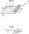
- Figure 16illustrates another method to expand the beam along both axes utilizing a double LOE configuration.
- the input waveis coupled into the first LOE 20a by the first reflecting surface 16a and then propagating along the ⁇ axis.
- the partially reflecting surfaces 22acouple the light out of 20a and then the light is coupled into the second LOE 20b by the reflecting surface 16b.
- the lightis then propagates along the ⁇ axis, and then coupled out by the selectively reflecting surfaces 22b.
- the original beamis expanded along both axes where the overall expansion is determined by the ratio between the lateral dimensions of the elements 16a and 22b respectively.
- the configuration given in Fig. 16is just an example of a double-LOE setup.
- Another issue to be addressedis the brightness of the system. This issue is important for see-through applications, where it is desired that the brightness of the display will be comparable to that of the external scene, to allow acceptable contrast ratio and convenient observation through the combiner. It is not possible to ensure that the insertion loss of most of the systems is small. For example, as described above for the four-surface combiner of Fig. 14 , because of the requested beam expansion along the ⁇ axis, the brightness of the optical waves is reduced four-fold. In general for N -reflecting surfaces the brightness reduces by a factor of N . In principle high-brightness display sources can offset this difficulty, but this approach necessarily has a practical limitation.
- each reflecting surface of the overall array of selectively reflecting surfaces 22is illuminated by only the part of the overall FOV.
- the reflectance of each surfacecan be set to optimize the brightness of the entire FOV.
- the reflectance of the right surface 22a in Fig. 11could be designed to have higher reflectance for the right part of the FOV and the lowest possible reflectance for the left part of the FOV, while the left surface 22b have higher reflectance for the left part of the FOV.
- a similar design methodcan be applied to a two-dimensional expansion system.
- the reflectance of the reflecting surfaces 22acould be designed such that the lower surfaces will have higher reflectance for the lower part of the FOV and the lowest possible reflectance for the higher part of the FOV, while the upper surfaces have higher reflectance for the upper part of the FOV. Therefore, the factor in which the brightness is reduced because of the lateral expansion can be much smaller than R, where R is the ratio between the area of the coupling-in surface 16a and the coupling-out surfaces 22b.
- Another method to improve the overall brightness of the systemis by controlling the display source brightness without changing the input power. As shown in Fig. 11 above, a large portion of the energy coupled onto the substrate 20 by the reflecting mirror 16 is reflected into the vicinity of the eye pupil 60. To maximize the achievable brightness, however, it is also desirable that most of the light that emerges from the display source couples into the substrate.
- Figure 17illustrates an example of a substrate-mode display where the display source is a transmission LCD.
- the lightwhich emerges from the light source 64 and collimated by a lens 66, illuminates an LCD 68.
- the image from the LCDis collimated and reflected by the optical components 70 onto the substrate 20.
- Figure 18illustrates an optical layout of the collimating/folding lens 70
- Fig. 19illustrates the foot-print of the light, which is coupled into the substrate 20, on the front surface 72 of the lens 70.
- there is a Lambertian distribution of the lightwhich emerges from the display. That is, the energy is distributed uniformly over the entire angular spectrum of 2 ⁇ steradians. As can be seen in Figs.
- a conventional diffuserscatters the light uniformly in all directions.
- a selective diffusercan spread the light in such a way that the light from each point source diverges into a required angular cone. In this case the power that the LCD surface illuminates remains the same. For a 20-30° cone, the diverging angle of the light for each point source is reduced by a factor of more than 50 as compared to the ⁇ steradians of the Lambertian source, the brightness of the light increases by the same factor. Hence, a significant improvement in the brightness of the system can be achieved with a minimal design and manufacturing effort and without increasing the power consumption of the system.
- An alternative solutionwhich is appropriate not only to LCDs but also to other display sources, is to use an array of micro-lenses that is aligned with the pixels of the display source. For each pixel a micro-lens narrows the diverging beam that emerges from that pixel into the desired angular cone. In fact, this solution is efficient only if the fill-factor of the pixels is a small number.
- An improved version of this solutionis to design the emitting distribution function of the pixels in the pixel-array to make each pixel diverge into the required angle. For example, in OLED displays, efforts are usually made to increase the divergence angle of the single LEDs in order to allow viewing from a wide angle. For our specific LOE display application, however, it is advantageous to keep this divergence angle small, in the order of 20-30°, to optimize the brightness of the system.
- EMBeye-motion-box
- Figure 21illustrates a possible solution to this problem.
- the two horizontal edges of the platesare replaced with two pairs of parallel reflecting surfaces, 88a, 88b and 90a, 90b respectively.
- the central part of the FOVprojects directly through to the aperture 84 as before, the rays from the lower part of the FOV are reflected from surfaces 88a and 88b, while the rays from the upper part of the FOV are reflected from surfaces 90a and 90b.
- the angles between the rays trapped inside the substrate and the reflecting surfaces 88 and 90are sufficiently large to affect total internal reflections, so no special reflecting coating is required for these surfaces. Since all rays are either traveling directly from the input aperture or reflected twice from a pair of parallel surfaces, the original direction of each ray is maintained, and the original image is not affected.
- the present exampleprovides for an FOV of 42° with a significantly reduced input aperture 84: 40 mm.
- a cascade of two or more pairs of reflecting surfacescan be used to achieve the desired FOV while maintaining an acceptable input aperture.
- Fig. 21is just an example illustrating a simple implementation of this method.
- the use of pairs of parallel reflecting surfaces in order to decrease the aperture of the system for a given FOV, or alternatively to increase the useable FOV for a given aperture,is not limited to substrate-mode optics and it can be utilized in other optical systems including, but not limited to, free-space systems like head-up displays, episcops or periscopes.
- the lateral dimension of the input aperture of the substrateis 40 mm along the ⁇ axis and 8.5 mm along the ⁇ axis.
- Figures 22A and 22Billustrate an alternative embodiment to that described above with reference to Figs. 14-15 .
- This approachinvolves an adjustment between a symmetrical collimating lens 6 and an asymmetrical input aperture.
- the lateral dimensions of the input apertureare assumed to be D and 4D along the two axes respectively.
- a lens 6 with an aperture of 2Dcollimates the image onto the substrate.
- the front half of the collimated lightis coupled into the substrate by the mirror 16a.
- Two pairs of parallel reflecting surfaces, 22a; 22b and 22c; 22dsplit the coupled light outward and then reflects it back to its original direction.
- the rear part of the collimated lightpasses through the substrate 20 and then folded by the prism 99 back into the substrate.
- a second mirror 16bcouples the folded light onto the substrate 20.
- the lateral dimensions of the input apertureare D and 4D along the two axes respectively, as required.
- FIG. 23illustrates an embodiment of the present invention in which the LOE 20 is embedded in an eye-glasses frame 100.
- the display source 4, the collimating lens 6, and the folding lens 70are assembled inside the arm portions 102 of the eye-glasses frame, just next to the edge of the LOE 20.
- the display sourceis an electronic element such as a small CRT, LCD, or OLED
- the driving electronics 104 for the display sourcemight be assembled inside the back portion of the arm 102.
- a power supply and data interface 106is connectable to arm 102 by a lead 108 or other communication means including radio or optical transmission.
- a battery and miniature data link electronicscan be integrated in the eye-glasses frame.
- the embodiment described abovecan serve in both see-through and non-see-through systems. In the latter case opaque layers are located in front of the LOE. It is not necessary to occlude the entire LOE, typically only the active area, where the display is visible needs to be blocked. As such, the device can ensure that the peripheral vision of the user is maintained, replicating the viewing experience of a computer or a television screen, in which such peripheral vision serves an important cognitive function.
- a variable filtercan be placed in front of the system in such a way that the viewer can control the level of brightness of the light emerging from the external scene.
- This variable filtercould be either a mechanically controlled device such as a folding filter, or two rotating polarizers, an electronically controlled device, or even an automatic device, whereby the transmittance of the filter is determined by the brightness of the external background.
- an LOEcan be utilized in this embodiment.
- the simplest optionis to use a single element for one eye.
- Another optionis to use an element and a display source for each eye, but with the same image.
- Yet another possibilityis to project two different scenes, one to each eye, in order to create a stereoscopic image.
- attractive implementationsare possible, including 3-dimensional movies, advanced virtual reality, training systems and others.
- Fig. 23is just an example illustrating the simple implementation of the present invention. Since the substrate-guided optical element, constituting the core of the system, is very compact and lightweight, it could be installed in a vast variety of arrangements. Hence, many other embodiments are also possible including a visor, a folding display, a monocle, and many more. This embodiment is designated for applications where the display should be near-to-eye: head-mounted, head-worn or head-carried. There are, however, applications where the display is located differently.
- An example of such an applicationis a hand-held device for mobile application, such as for example a cellular phone.
- Figure 24illustrates an alternative method, based on the present invention, which eliminate the current compromise between the small size of mobile devices and the desire to view digital content on a full format display, by projecting high quality images directly into the eye of the user.
- An optical module including the display source 6, the folding and collimating optics 70 and the substrate 20is integrated into the body of a cellular phone 110, where the substrate 20 replaces the existing protective cover-window of the phone.
- the volume of the support components including source 6 and optics 70is sufficiently small to fit inside the acceptable volume for modern cellular devices.
- the userpositions the window in front of his eye 24, to conveniently view the image with high FOV, a large eye-motion-box and a comfortable eye-relief.
- the optical modulecan operate in see-through configuration, a dual operation of the device is possible; namely it is optionally possible to maintain the conventional cellular display 112 intact. In this manner the standard, low-resolution display can be viewed through the LOE when the display source 6 is shut-off.
- a second modedesignated for e-mail reading. Internet surfing, or video operation, the conventional display 112 is shut-off while the display source 6 projects the required wide FOV image into the viewer's eye through the LOE.
- the embodiment described in Fig. 24is only an example, illustrating that applications other than head-mounted displays can be materialized.
- Other possible hand-carried arrangementsinclude palm computers, small displays embedded into wristwatches, a pocket-carried display having the size and weight reminiscent of a credit card, and many more.
- HUDhead-up displays
- LOE-based HUDpotentially provide the possibilities for a very compact, self-contained HUD, that can be readily installed in confined spaces. It also simplifies the construction and manufacturing of the optical systems related to the HUD and therefore is a potentially suitable for both improving on aerospace HUD's, as well as introducing a compact, inexpensive, consumer version for the automotive industry.
- Fig. 25illustrates a method of materializing an HUD system based on the present invention.
- the light from a display source 4is collimated by a lens 6 to infinity and coupled by the first reflecting surface 16 into substrate 20. After reflection at a second reflecting array (not shown), the optical waves impinge on a third reflecting surfaces 22, which couples the light out into the eyes 24 of the viewer.
- the overall systemcan be very compact and lightweight, of the size of a large postcard having a thickness of a few millimeters.
- the display sourcehaving a volume of a few cubic centimeters, can be attached to one of the corners of the substrate, where an electric wire can transmit the power and data to the system. It is expected that the installation of the presented HUD system will not be more complicated than the installation of a simple commercial audio system. Moreover, since there is no need for an external display source for image projection, the necessity to install components in unsafe places is avoided.
- FIG. 25can be implemented for other applications, in addition to HUD systems for vehicles.
- One possible utilization of these embodimentsis as a flat display for a computer or television.
- the main unique characteristic of such a displayis that the image is not located at the screen plane, but is focused at infinity or to a similarly convenient distance.
- One of the main drawbacks of existing computer displaysis that the user has to focus his eyes at a very close distance of between 40 and 60 cm, while the natural focus of a healthy eye is to infinity.
- Many peoplesuffer from headaches after working for a long duration of time at a computer. Many others who work frequently with computers tend to develop myopia.
- some people, who suffer from both myopia and hyperopianeed special spectacle for work with a computer.
- a flat display, based on the present inventioncould be an appropriate solution for people who suffer from the above-described problems and do not wish to work with a head-mounted display.
- the present inventionallows for a significant reduction in the physical size of the screen.
- the image formed by the LOEis larger than the device, it would be possible to implement large screens on smaller frames. This is particularly important for mobile applications such as lap and palm-top computers.
- LOErelates to its brightness. Ideally, for compactness it is advantageous to use a miniature display source, but this necessarily reduces the display brightness due to the large increase in the actively illuminated area of the LOE as compared to the actively illuminated area of the source. Therefore, even after the special measures described in the foregoing are deployed, one expects a reduction in the brightness, even for non- see through applications. This reduction in the brightness can be offset either by increasing the brightness of the source, or deploying more than one source. That is, the LOE can be illuminated with an array of display sources and their associated collimating lenses. Fig. 26 illustrates an example of this method.
- Another advantage of the LOE display of the present inventionis its very flat shape, even compared to the existing flat-panel displays. Another difference is a significantly more directional viewing angle: the LOE display can be viewed from a significantly limited angular range as compared to common flat-panel display. Such limited head-motion-box is sufficient for convenient operation by a single user, and offers the additional advantages of privacy in many situations.
- the image of the LOE-based screenis located in a distant plane behind the display surface and not on its physical surface.
- the sensation of the imageis similar to viewing it through a window.
- This configurationis particularly suitable for implementing three-dimensional displays.
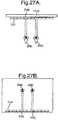
- Figures 27A and 27Billustrate a front view and a top view, respectively, of a possible configuration, based on the present invention to materialize a real 3-D display.
- an array 114 of n different display sources 114, 114 nis located at the lower portion of the substrate 20, where each display source projects images obtained at different perspectives of the same scene.
- the image from each display sourceis coupled into the substrate in the same manner as described above with reference to Fig. 26 .
- his right 24a and left 24b eyesview the images projected from the display sources 114i and 114j, respectively. Consequently the viewer sees with each eye the same scene from a different perspective.
- the experienceclosely resembles the viewing experience when observing a real 3-D object through a window.
- Figs. 28a- 28bwhen the viewer moves his gaze horizontally his eyes see the images which are projected from different display sources 114k and 114 l ; the effect is similar to moving the head across a window while looking at an external scene.
- Figs. 29A-29BWhen the viewer moves his gaze vertically, as illustrated in Figs. 29A-29B , the eyes see points on the screen which are located lower then before. Since these points are located closer to the display sources 114, the viewer sees images which emerge from different display sources 114g and 114h, which are located closer to the center of the array 114 than before. As a result, the sensation of the viewer is similar to viewing a scene, which is closer to the window. That is, the scene through the substrate is seen as a three-dimensional panorama where the lower part of the scene is closer to the viewer.
- Another possible embodiment of the inventionis its implementation as a teleprompter, such as used as to project text to a speaker or TV broadcaster; as the teleprompter is transparent, the audience feel that the speaker is making eye-contact with them while he is actually reading text.
- the telepromptercan be implemented with a small source, attached to the optical assembly, alleviating the need to locate large screen in the vicinity of the device.
- Yet another possible implementation of this embodimentis as a screen for a personal digital assistance (PDA).
- PDApersonal digital assistance
- the size of the existing conventional screens which are presently used,is under 10 cm. Since the minimal distance where these displays can be read is on the order of 40 cm, the obtainable FOV is under 15°; hence, the information content, especially as far as text is concerned, on these displays is limited.
- a significant improvement in the projected FOVcan be made with the embodiment illustrated in Fig. 24 .
- the imageis focused at infinity, and the screen can be located much closer to the eyes of the viewer.
- TFOVtotal filed-of-view
- another increase in the TFOVmay be achieved. Therefore, a display with an FOV of 40° or larger is feasible.
- the image which was transmitted by the substrate 20originated from an electronic display source such as a CRT or LCD.
- an electronic display sourcesuch as a CRT or LCD.
- the transmitted imagecan be a part of a living scene, for example, when it is required to couple a living scene onto an optical system.
- Fig. 30illustrates an application of star-light amplifier (SLA) 116 where this implementation is required.
- SLAstar-light amplifier
- the image from the external sceneis focused by the collimator 118 into the SLA where the electronic signal of the image is amplified to create a synthetic image which is projected through an eye-piece 120 onto the viewer eye.
- the illustrated configurationis fairly popular for military, para-military and civilian applications. This commonly used configuration necessarily protrudes forward in front of the user and makes it inconvenient for protracted use in a head-mounted configuration.
- the deviceis relatively heavy and in addition to its physically interference with objects in the vicinity of the user, and it exerts a strenuous moment on the user's head and neck.
- FIG. 31A more convenient configuration is illustrated in Fig. 31 .
- the deviceis not located in front of the user but to the side of the head, where the center of the gravity of the SLA is aligned along the main axis of the head.
- the direction of the deviceis reversed, that is, the collimator 118 is located at the rear and the eye-piece 120 is located at the front.
- the image from the frontal external sceneis coupled into the collimator 118 by using an LOE 20a, where the image from the eye-piece 120 is coupled into the user's eye by using another LOE 20b.
- additional two optical elements, 20a and 20bare added to the original device, the weight of these elements is negligible compared to the weight of the SLA and the overall configuration is much more convenient than before.
- these two elementsbe configures as modular so that they can be either shifted away from their position or even removed by the user.
- the SLA viewercan he reconfigured for convenient location for head-mounted operation with the LOE mounted, or for mounting on standard gun-sites or other aiming devices for use without the LOE modules. It is also possible to shift the LOE's so as to accommodate the use of the device with either eye.
- the LOEis utilized to transmit light waves for imaging purposes:
- the present inventioncan be applied not only for imaging, but also for non-imaging applications, mainly illumination systems, in which the optical quality of the output wave is not crucial and the important parameters are intensity and uniform brightness.
- the inventionmay be applied, for example, in back illumination of flat-panel displays, mostly LCD systems, in which, in order to construct an image, it is necessary to illuminate the plate with a light as bright and uniform as possible.
- Other such possible applicationsinclude, but are not limited to, flat and non-expensive substitutes for room illumination or for floodlights, illuminators for fingerprint scanners, and readout waves for 3-dimensional display holograms.
- FIG.32illustrates an example of a substrate-mode display where the display source is a reflection LCD.
- the light generated by an illuminator 122passes through a polarizer 124, collimated by a lens 126, reflected by a polarizing beamsplitter 128 and illuminates an LCD 130.
- the polarisation of the light which is reflected from the LCDis rotated in 90° by a 1 ⁇ 4 wavelengths plate, or alternatively by the LCD material itself.
- the image from the LCDnow passes through the beamsplitter to be collimated and reflected by the lens 132 onto the substrate 20.
- the entire illuminating systemis large and cumbersome, and certainly not compact enough for head-mounted systems.
- the collimating lens 132is located further away from the display source, while for the sake of minimizing the aberrations it is required that the field-lens will be located as close as possible to the display surface.
- Fig. 33An improved version of the illuminating setup is illustrated in Fig. 33 .
- the light from the light source 122coupled into another LOE 134, which illuminates the surface of the LCD 130, where the partially reflective surfaces are polarizing sensitive.
- the entire system hereis much more compact than that illustrated in Fig. 32 , and the lens 132 is located much closer to the LCD surface.
- the input aperture of the LOE 134is much smaller than that of the beamsplitter 128, the collimating lens 126 can be now much smaller than before, and therefore have a larger f-number.
- the illuminating arrangement shown in Fig. 32is only an example. Other arrangements for illuminating a reflective or transmission LCD, or for using for any other illuminating purposes in accordance with the optical system and the desired parameters, are also permissible.
- Fig. 34illustrates a possible method of fabricating an array of partially reflecting surfaces.
- the surfaces of a plurality of transparent flat plates 138are coated with the required coatings 140 and then the plates are cemented together so as to create a stack form 142.
- a segment 144is then sliced off the stack form by cutting, grinding and polishing, to create the desired array of reflecting surfaces 146, which can be assembled with other elements to materialize the entire LOE. More than one array 146 can be fabricate of each segment 144, according to the actual size of the coated plates 138 and the required size of the LOE. As described in Figs.
- the required coatings of the selectively reflecting surfacesshould have a specific angular and spectral response in order to assure a proper operation of the LOE. Hence, it is essential to accurately measure the actual performance of the coatings before the final fabrication of the LOE. As explained above, there are two angular regions that should be measured - the high incident angles (usually between 60° and 85°) where the reflectance is very low and the low incident angles (usually between 15° and 40°), where the reflectance of the surfaces is utilized to couple part of the trapped waves out of the LOE. Naturally, the coating should be measured at these two regions.
- the main problem of the testing procedureis that it is very difficult to measure with the existing testing equipment the reflectance (or alternatively the transmission) for very high angles of incidence, usually above 60°, for coatings that are located, as in our case, between two transparent plates.
- the other part of the beamis reflected from the coated surface, reflected again by total internal reflection from the external surface of the lower prism, impinges at the coated surface again at an angle 3 ⁇ , reflected again from the external surface of the upper prism by total internal reflection, and then reflected by the coated surface at an angle ⁇ and coupled out from the prism.
- the intensity of the output beam 158can be measured. Taking into account the Fresnel reflections, the intensity of the output beam is ( R ⁇ ) 2 * T' 3 ⁇ . Hence, knowing the reflectance R ⁇ from the previous step, the reflectance at an angle 3 ⁇ can be calculated accordingly.
- Figure 36illustrates a folding prism 160 used to translate the beam into that of the original beam. The residue of the original ray 154 can be blocked using a suitable mask or blocking layer 162.
- each pair of prismscan measure the reflectance at two angles - ⁇ and 3 ⁇ .
- the head angleis 25° then the reflectance at 25° and 75° can be measured simultaneously. Therefore, a small number of prism pairs (2 or 3) is usually requested for a proper measurements of the coated plates.
- the setup shown herecan be utilized to measure the reflectance of these two angles at different wavelengths as well as for the two polarizations, if required.
- an optical devicefor partially reflecting a first set of light waves having a given polarization state and located within a given optical spectrum and within a first angular spectrum, and transmitting a second set of light waves having the same given polarization state and located within the same given optical spectrum and within a second angular spectrum, comprising a first light-transmitting substrate having a surface (22), wherein a dichroic coating is disposed on said surface (22) and in that angles located within said first angular spectrum are smaller than angles located within said second angular spectrum and that the reflectivity by the coated surface (22) of said first set of light waves is higher than the reflectivity by the coated surface (22) of said second set of light waves.
- the optical device of the other aspect of the inventionfurther comprises a second light-transmitting substrate (20) optically coupled to the first light-transmitting substrate at the coated surface (22).
- the polarization stateis the P polarization
- the polarization stateis a combination of the S and the P polarizations.
- the reflectance of the first set of light wavespreferably changes monotonically with increasing incident angles at the surface (22).
- the reflectance of the first set of light wavesdecreases monotonically with increasing incident angles at the surface (22), while in a second preferred variation, the reflectance of the first set of light waves increases monotonically with increasing incident angles at the surface (22).
- the optical spectrumis advantageously located within the visual spectrum.
- the optical spectrumis located within the region between 460 nm and 640 nm.
- the first angular spectrumis preferably located within the region between 15° and 40°.
- the second angular spectrumis preferably located within the region between 50° and 80°.
- a specific minimal reflectanceis set for the first angular spectrum.
- the reflectivity by the coated surface (22) of the first set of light wavesis advantageously higher than the specific minimal reflectance and/or the reflectivity of the specific minimal reflectance is preferably higher than 20%.
- a specific maximal reflectanceis set for the second angular spectrum.
- the reflectivity by the coated surface (22) of the second set of light wavesis advantageously lower than the specific maximal reflectance and/or the reflectivity of the specific maximal reflectance is advantageously lower than 10%.
Landscapes
- Physics & Mathematics (AREA)
- General Physics & Mathematics (AREA)
- Optics & Photonics (AREA)
- Spectroscopy & Molecular Physics (AREA)
- Engineering & Computer Science (AREA)
- Manufacturing & Machinery (AREA)
- Laser Surgery Devices (AREA)
- Optical Couplings Of Light Guides (AREA)
- Light Guides In General And Applications Therefor (AREA)
- Devices For Indicating Variable Information By Combining Individual Elements (AREA)
- Liquid Crystal (AREA)
- Surface Treatment Of Glass Fibres Or Filaments (AREA)
- Mechanical Optical Scanning Systems (AREA)
- Optical Head (AREA)
- Non-Portable Lighting Devices Or Systems Thereof (AREA)
- Planar Illumination Modules (AREA)
- Optical Elements Other Than Lenses (AREA)
Abstract
Description
- The present invention relates to substrate-guided optical devices, and, particularly to devices which include a plurality of reflecting surfaces carried by a common light-transmissive substrate, also referred to as a light-guide.
- The invention can be implemented to advantage in a large number of imaging applications, such as, for example, head-mounted and head-up displays, cellular phones, compact displays, 3-D displays, compact beam expanders as well as non-imaging applications such as flat-panel indicators, compact illuminators and scanners.
- One of the important applications for compact optical elements is in head-mounted displays wherein an optical module serves both as an imaging lens and a combiner, in which a two-dimensional display is imaged to infinity and reflected into the eye of an observer. The display can be obtained directly from either a spatial light modulator (SLM) such as a cathode ray tube (CRT), a liquid crystal display (LCD), an organic light emitting diode array (OLED), or a scanning source and similar devices, or indirectly, by means of a relay lens or an optical fiber bundle. The display comprises an array of elements (pixels) imaged to infinity by a collimating lens and transmitted into the eye of the viewer by means of a reflecting or partially reflecting surface acting as a combiner for non-see-through and see-through applications, respectively. Typically, a conventional, free-space optical module is used for these purposes. Unfortunately, as the desired field-of-view (FOV) of the system increases, such a conventional optical module becomes larger, heavier, bulkier and therefore, even for moderate performance device, impractical. This is a major drawback for all kinds of displays but especially in head-mounted applications, wherein the system must necessarily be as light and as compact as possible.
- The strive for compactness has led to several different complex optical solutions, all of which, on the one hand, are still not sufficiently compact for most practical applications, and, on the other hand, suffer major drawbacks in terms of manufacturability. Furthermore, the eye-motion-box of the optical viewing angles resulting from these designs is usually very small - typically less than 8 mm. Hence, the performance of the optical system is very sensitive, even to small movements of the optical system relative to the eye of the viewer, and do not allow sufficient pupil motion for conveniently reading text from such displays.
- The present invention facilitates the design and fabrication of very compact light-guide optical elements (LOE) for, amongst other applications, head-mounted displays. The invention allows relatively wide FOV's together with relatively large eye-motion-box values.
- The resulting optical system offers a large, high-quality image which also accommodates large movements of the eye. The optical system offered by the present invention is particularly advantageous because it is substantially more compact than state-of-the-art implementations and yet it can be readily incorporated, even into optical systems having specialized configurations.
- The invention also enables the construction of improved head-up displays (HUDs). Since the inception of such displays more than three decades ago, there has been significant progress in the field. Indeed, HUDs have become popular and they now play an important role, not only in most modern combat aircraft, but also in civilian aircraft, in which HUD systems have become a key component for low-visibility landing operation. Furthermore, there have recently been numerous proposals and designs for HUDs in automotive applications where they can potentially assist the driver in driving and navigation duties. Nevertheless, state-of-the-art HUDs suffer several significant drawbacks. All HUD's of the current designs require a display source that must be offset a significant distance from the combiner to ensure that the source illuminates the entire combiner surface. As a result, the combiner-projector HUD system is necessarily bulky, and large, and requires a considerable installation space, which makes it inconvenient for installation and at times even unsafe to use. The large optical aperture of conventional HUDs also pose a significant optical design challenge, rendering the HUD's with either a compromising performance, or leading to high cost wherever high-performance is required. The chromatic dispersion of high-quality holographic HUD's is of particular concern.
- An important application of the present invention relates to its implementation in a compact HUD, which alleviates the aforementioned drawbacks. In the HUD design of the current invention, the combiner is illuminated with a compact display source that can be attached to the substrate. Hence, the overall system is very compact and can be readily installed in a variety of configurations for a wide range of applications. In addition, the chromatic dispersion of the display is negligible and, as such, can operate with wide spectral sources, including a conventional white-light source. In addition, the present invention expands the image so that the active area of the combiner can be much larger than the area that is actually illuminated by the light source.
- Another important application of the present invention is in providing for a large screen with a true three-dimensional (3-D) view. Ongoing developments in information technology have led to an increasing demand for 3-D displays. Indeed, a broad range of 3-D equipment is already on the market. The available systems, however, require users to wear special devices to separate the images intended for left eye and the right eye. Such "aided viewing" systems have been firmly established in many professional applications. Yet further expansion to other fields will require "free viewing" systems with improved viewing comfort and closer adaptation to the mechanisms of binocular vision. State-of-the-art solutions to this problem suffer from various disadvantages and they fall short familiar 2-D displays in terms of image quality arid viewing comfort. However, using the present invention it is possible to implement a real high-quality 3-D autostereoscopic display that requires no viewing aids and that can readily be fabricated with standard optical manufacturing processes.
- A further application of the present invention is to provide a compact display with a wide FOV for mobile, hand-held application such as cellular phones. In today's wireless internet-access market, sufficient bandwidth is available for full video transmission. The limiting factor remains the quality of the display within the end-user's device. The mobility requirement restricts the physical size of the displays, and the result is a direct-display with a poor image viewing quality. The present invention enables, physically very compact display with a very large virtual image. This is a key feature in mobile communications, and especially for mobile Internet access, solving one of the main limitations for its practical implementation. Thereby the present invention enables the viewing of the digital content of a full format Internet page within a small, hand-held device, such as a cellular phone.
- The broad object of the present invention, therefore, is to alleviate the drawbacks of state-of-the-art compact optical display devices and to provide other optical components and systems having improved performance, according to specific requirements.
- The invention therefore provides an optical device an optical device, comprising a light-transmitting substrate having at least two major surfaces and edges; optical means for coupling light into said substrate by total internal reflection, and at least one partially reflecting surface located in said substrate.
- The invention is described in connection with certain preferred embodiments, with reference to the following illustrative figures so that it may be more fully understood.
- With specific reference to the figures in detail, it is stressed that the particulars shown are by way of example and for purposes of illustrative discussion of the preferred embodiments of the present invention only, and are presented in the cause of providing what is believed to be the most useful and readily understood description of the principles and conceptual aspects of the invention. In this regard, no attempt is made to show structural details of the invention in more detail than is necessary for a fundamental understanding of the invention. The description taken with the drawings are to serve as direction to those skilled in the art as to how the several forms of the invention may be embodied in practice.
- In the drawings:
Fig. 1 is a side view of a generic form of prior art folding optical device;Fig. 2 is a side view of an exemplary light-guide optical element in accordance with the present invention;Figs. 3A and 3B illustrate the desired reflectance and transmittance characteristics of selectively reflecting surfaces used in the present invention for two ranges of incident angles;Fig. 4 illustrates the reflectance curves as a function of wavelength for an exemplary dichroic coating;Fig. 5 illustrates a reflectance curve as a function of incident angle for an exemplary dichroic coating;Fig. 6 illustrates the reflectance curves as a function of wavelength for another dichroic coating;Fig. 7 illustrates a reflectance curve as a function of incident angle for another dichroic coating;Fig. 8 is a schematic sectional-view of a reflective surface according to the present invention;Figs. 9A and 9B are diagrams illustrating detailed sectional views of an exemplary array of selectively reflective surfaces;Fig. 10 is a diagram illustrating a detailed sectional view of an exemplary array of selectively reflective surfaces wherein a thin transparent layer is cemented at the bottom of the light-guide optical element;Fig. 11 illustrates detailed sectional views of the reflectance from an exemplary array of selectively reflective surfaces, for three different viewing angles;Fig. 12 is a sectional view of an exemplary device according to the present invention, utilizing a half-wavelength plate for rotating the polarization of incoming light;Fig. 13 shows two graphs representing simulated calculations for the brightness as a function of FOV across the image of the projected display, and the external (see-through) scene;Fig. 14 is a diagram illustrating a light-guide optical element (LOE) configuration having an array of four partially reflecting surfaces, according to the present invention;Fig. 15 is a diagram illustrating a light-guide optical element configuration having an array of four partially reflecting surfaces, according another embodiment of the present invention;Fig. 16 is a diagram illustrating a method to expand a beam along both axes utilizing a double LOE configuration;Fig. 17 is a side view of a device according to the present invention, utilizing a liquid-crystal display (LCD) light source;Fig. 18 is a diagram illustrating an optical layout of a collimating and folding optical element according to the present invention;Fig. 19 is a diagram illustrating the footprint of the light, which is coupled into the substrate, on the front surface of the collimating lens according to the present invention;Fig. 20 is a diagram illustrating an equivalent, unfolded diagram of an optical layout according to the present invention;Fig. 21 is a diagram illustrating a diagram of an optical layout according to the present invention utilizing two pairs of parallel reflecting mirrors to achieve a wide field of view;Fig. 22A is a top view and 22B is a side view of an alternative configuration for expanding light according to the present invention;Fig. 23 illustrates an exemplary embodiment of the present invention embedded in a standard eye-glasses frame;Fig. 24 is a diagram illustrating an exemplary method for embedding an embodiment of the present invention within a mobile hand-held device such as a cellular telephone;Fig. 25 illustrates an exemplary HUD system in accordance with the present invention;Fig. 26 illustrates an exemplary embodiment of the present invention where the light-guide optical element is illuminated with an array of display sources;Figs. 27- 29 are diagrams illustrating exemplary embodiment of an imaging system which projects a three-dimensional image to the eyes of a viewer, according to the present invention;Fig. 30 illustrates an embodiment for conventional implementation of a star's-light amplifier (SLA) device;Fig. 31 illustrates an exemplary embodiment for an improved implementation of star's-light amplifier (SLA) using devices according to the present invention;Fig. 32 is a side view of a device according to the present invention, utilizing a reflective liquid-crystal display (LCD) display source with a, conventional illuminating device;Fig. 33 is a side view of a device according to the present invention, utilizing a reflective liquid-crystal display (LCD) display source in which a light-guide element is used for illuminating the source;Fig. 35 is a diagram illustrating a method for fabricating an array of selectively reflecting surfaces according to the present invention;Fig. 35 is a diagram illustrating a measurement arrangement utilizing two prisms to measure the reflectance of a coated plate at two different angles, andFig. 36 is a diagram illustrating a measurement system utilizing two prisms to measure the reflectance of a coated plate at two different angles further employing a folding prism to align the second output beam with the incident input beam.Fig. 1 illustrates a conventional folding optics arrangement, wherein thesubstrate 2 is illuminated by adisplay source 4. The display is collimated by acollimating lens 6. The light from thedisplay source 4 is coupled intosubstrate 2 by a first reflectingsurface 8, in such a way that themain ray 10 is parallel to the substrate plane. A second reflectingsurface 12 couples the light out of the substrate and into the eye of aviewer 14. Despite the compactness of this configuration, it suffers significant drawbacks; in particular only a very limited FOV can be affected. As shown inFig. 1 , the maximum allowed off-axis angle inside the substrate is:
- whereinT is the substrate thickness;
- deye is the desired exit-pupil diameter, and
- l is the distance between reflecting
surfaces - With angles higher than αmax the rays are reflected from the substrate surface before arriving at the reflecting
surface 12. Hence, the reflectingsurface 12 will be illuminated at an undesired direction and ghost images appear. - Therefore, the maximum achievable FOV with this configuration is:

- Typically the refractive index values lie in the range of 1.5-1.6.
- Commonly, the diameter of the eye pupil is 2-6 mm. To accommodate movement or misalignment of the display, a larger exit-pupil diameter is necessary. Taking the minimum desirable value at approximately 8-10 mm, the distance between the optical axis of the eye and the side of the head,l, is, typically, between 40 and 80 mm. Consequently, even for a small FOV of 8° the desired substrate thickness would be of the order of 12 mm.
- Methods have been proposed to overcome the above problem. These include, utilizing a magnifying telescope inside the substrate and non-parallel coupling directions. Even with these solutions, however, and even if only one reflecting surface is considered, the system thickness remains limited by a similar value. The FOV is limited by the diameter of the projection of the
reflective surface 12 on the substrate plane. Mathematically, the maximum achievable FOV, due to this limitation, is expressed as:
- whereinαsur is the angle between the reflecting surface and the normal to the substrate plane, and
- Reye is the distance between the eye of the viewer and the substrate (typically, about 30-40 mm).
- Practically tanαsur cannot be much larger than 1; hence, for the same parameters described above for a FOV of 8° the required substrate thickness here is on the order of 7 mm, which is an improvement on the previous limit. Nevertheless, as the desired FOV is increased, the substrate thickness increases rapidly. For instance, for desired FOVs of 15° and 30° the substrate limiting thickness is 18 mm or 25 mm, respectively.
- To alleviate the above limitations, the present invention utilizes an array of selectively reflecting surfaces, fabricated within a light-guide optical element (LOE).
Fig. 2 illustrates a sectional view of an LOE according to the present invention. The first reflectingsurface 16 is illuminated by a collimateddisplay 18 emanating from a light source (not shown) located behind the device. The reflectingsurface 16 reflects the incident light from the source such that the light is trapped inside aplanar substrate 20 by total internal reflection. After several reflections from the surfaces of the substrate, the trapped waves reach an array of selectively reflectingsurfaces 22, which couple the light out of the substrate into the eye of aviewer 24. Assuming that the central wave of the source is coupled out of thesubstrate 20 in a direction normal to thesubstrate surface 26, and the off-axis angle of the coupled wave inside thesubstrate 20 isαin, then the angleαsur2 between the reflecting surfaces and the substrate plane is:
- As can be seen in
Fig. 2 , the trapped rays arrive at the reflecting surfaces from twodistinct directions directions 28 after an even number of reflections from the substrate surfaces 26, wherein the incident angleβref between the trapped ray and the normal to the reflecting surface is:
- The trapped rays arrive at the reflecting surface from the
second direction 30 after an odd number of reflections from the substrate surfaces 26, where the off-axis angle isα'in = 180° -αin and the incident angle between the trapped ray and the normal to the reflecting surface is:
- In order to prevent undesired reflections and ghost images, it is important that the reflectance be negligible for one of these two directions. The desired discrimination between the two incident directions can be achieved if one angle is significantly smaller then the other one. Two solutions to this requirement, both exploiting the reflection properties of S-polarized light were previously proposed, however, both of these solutions suffer drawbacks. The main disadvantage of the first solution is the relatively large number of reflecting surfaces required to achieve an acceptable FOV. The main drawback of the second configuration is the undesired reflectance of the rays having an internal angle ofαin. An alternative solution is presently described, exploiting the reflection properties of P-polarized light and in some cases also the S-polarized light, and providing for a shallower reflecting surface inclination so that fewer reflecting surfaces are required for a given application.
- The reflection characteristics as a function of incident angle of S- and P-polarized light are different.. Consider for example an air/crown glass interface; while both polarizations reflect 4% at zero incidence, the Fresnel reflectance of S-polarized light incident on the boundary rises monotonically to reach 100% at grazing incidence, the Fresnel reflectance of P-polarized light first decreases to 0% at the Brewster's angle and only then rises to 100% at grazing incident. Consequently, one can design a coating with high reflectance for S-polarized light at an oblique incident angle and near-zero reflectance for a normal incidence. Furthermore one can also readily design a coating for a P-polarized light with very low reflectance at high incident angles and a high reflectance for low incident angles. This property can be exploited to prevent undesired reflections and ghost images as described above, by eliminating the reflectance in one of the two directions. For example choosingβref∼25° from Equations (5) and (6) it can be calculated that:

- If now a reflecting surface is determined for whichβ'ref is not reflected butβref is, the desired condition is achieved.
Fig: 3A and 3B illustrate the desired reflectance behavior of selectively reflecting surfaces. While the ray 32 (Fig. 3A ), having an off-axis angle ofβref∼25°, is partially reflected and is coupled out of thesubstrate 34, the ray 36 (Fig. 3B ), which arrives at an off-axis angle ofβ'ref∼75° to the reflecting surface (which is equivalent toβ'ref ∼105°), is transmitted through the reflectingsurface 34 without any notable reflection. Fig. 4 shows the reflectance curves of a dichroic coating designed to achieve the above reflectance characteristics, for four different incident angles: 20°, 25°, 30° and 75°, all of them for P-polarized light. While the reflectance of the high-angle ray is negligible over the entire relevant spectrum, the rays at off-axis angles of 20°, 25° and 30° obtain almost constant reflectance of 26%, 29% and 32% respectively, over the same spectrum. Evidently, reflectance decreases with the obliquity of the incident rays.Fig. 5 illustrates the reflectance curves of the same dichroic coating, as a function of the incident angle for P-polarized light with the wavelength λ=550 nm. Evidently, there are two significant regions in this graph: between 50° and 80° where the reflectance is very low and between 15° and 40° where the reflectance increases monotonically with decreasing incident angles. Hence, as long as, for a given FOV, one can ensure that the entire angular spectrum ofβ'ref, where very low reflections are desired, will be located inside the first region while the entire angular spectrum ofβref, where higher reflections are required, will be located inside the second region one can ensure the reflection of only one substrate modes into the viewer's eye and ensure a ghost-free image.- Up to now, only P-polarized light was analyzed. This treatment is sufficient for a system using a polarized display source, such as a liquid-crystal-display (LCD) or for a system where the output brightness is not crucial and the S-polarized light can be filtered out. However, for an unpolarized display source, like a CRT or an OLED, and where the brightness is critical, S-polarized light cannot be neglected and it must be taken into account during the design procedure. Fortunately, although it is more challenging than the P-polarized light, it is also possible to design a coating with the same behavior for an S-polarized light as discussed above. That is, a coating having a very low reflectance for an entire angular spectrum ofβ'ref and higher, pre-defined reflections for the respective angular spectrum ofβref.
Figs. 6 and 7 illustrate the reflectance curves of .the same dichroic coating described above with reference toFigs 4 and 5 , but now for S-polarized light. Apparently there are some differences between the behavior of the two poiarizations: the region of high angles where the reflectance is very low is much narrower for the S-polarization; it is much more difficult to achieve a constant reflectance for a given angle over the entire spectral bandwidth for the S-polarized light than for the P-polarized light; and finally, the monotonic behavior of the S-polarized light at the angular spectrum ofβref, where higher reflections are required, is opposite to that of the P-polarized light, that is, the reflectance for the S-polarized light increases with the obliquity of the incident rays. Apparently, this contradicting behavior of the two polarizations at the angular spectrum ofβref could be utilized during the optical design of the system to achieve the desired reflectance of the overall light according to the specific requirements of each system.- It is clear that the reflectance of the first reflecting surface 16 (
Fig. 2 ) should be as high as possible, so as to couple as much light as possible from the display source onto the substrate. Assuming that the central wave of the source is normally incident onto the substrate, i.e.,α0 =180°, then the angleαsur1 between the first reflecting surface and the normal to the substrate plane is:
- The solutions forαsur1 andα'sur1 in the above example are 155° and 1 15°, respectively.
Fig. 8 presents a sectional view of thereflective surface 16 which couples light 38 from a display source (not shown) and traps it inside thesubstrate 20 by total internal reflection. As plotted here, the projectionS1 of the reflecting surface on thesubstrate surface 40 is:
- The solution ofα =α'sur1 is preferred, since the coupling area on the substrate surface for the above example is more than 4.5 times larger than it is for the previous solutions. A similar improvement ratio holds for other systems. Assuming that the coupled wave illuminates the entire area of the reflecting surface, after reflection from the
surface 16, it illuminates an area of 2S1 = 2T tan(α) on the substrate surface. On the other hand, the projection of areflection surface 22 on the substrate plane, isS2S2 =T tan(αsur2). To avoid either overlapping or gaps between the reflecting surfaces, the projection of each surface is adjacent to its neighbor. Hence, the numberN of reflectingsurfaces 22 through which each coupled ray passes during one cycle (i.e., between two reflections from the same surface of the substrate) is:
- In this example, whereαsur2 = 65° andαsur1 = 115°, the solution isN = 2; that is, each ray passes through two different surfaces during one cycle. This is a conceptual change and a significant improvement over our previous disclosures, where each ray passes through six different surfaces during one cycle. The ability to reduce the number of reflecting surfaces for a given FOV requirement relates to the projection of the reflecting surface on the viewing plane - as the angles in the present disclosure are larger, fewer reflection surfaces are needed to span the image dimensions. Allowing fewer reflection surfaces simplifies the implementation of the LOE and insures a significant cost saving in its manufacture.
- The embodiment described above with regard to
Fig. 8 is an example of a method for coupling the input waves into the substrate. Input waves could, however, also be coupled into the substrate by other optical means, including (but not limited to) folding prisms, fiber optic bundles, diffraction gratings, and other solutions. - Also, in the example illustrated in
Fig. 2 , the input waves and the image waves are located on the same side of the substrate. Other configurations are envisioned in which the input and the image waves could be located on opposite sides of the substrate. It is also possible, in certain applications, to couple the input waves into the substrate through one of the substrate's peripheral sides. Fig. 9A is a detailed sectional view of an array of selectively reflective surfaces which couple light trapped inside the substrate out and into the eye of a viewer. As can be seen, in each cycle the coupled ray passes through reflectingsurfaces 42, having a direction ofα'in = 130°, whereby the angle between the ray and the normal to the reflecting surfaces is ∼75° and the reflections from these surfaces are negligible. In addition, the ray passes in each cycle twice through the reflectingsurface 44 having a direction ofαin = 50°, where the incident angle is 25° and part of the ray's energy is coupled out of the substrate. Assuming that one array of two selectively reflectingsurfaces 22 is used to couple the light onto the yiewer's eye, the maximal FOV is:
- Hence, for the same parameters of the examples above, the limiting substrate thickness for an FOV of 8° is in the order of 2.8 mm; for FOVs of 15° and 30°, the limiting substrate thickness is 3.7 mm and 5.6 mm, respectively. These are more favorable values than the limiting thickness of the state-of-the-art solutions discussed above. Moreover, more than two selectively reflecting surfaces can be used. For example, for three selectively reflecting
surfaces 22, the limiting substrate thickness for FOVs of 15° and 30° is approximately 2.4 mm and 3.9 mm, respectively. Similarly additional reflecting surfaces may be introduces to, amongst other advantages, reduce the limiting optical thickness further. - For configuration where a relatively small FOV is required, a single partially reflecting surface can be sufficient. For example, for a system with the following parameters:Reye = 25 mm;αsur = 72° and T = 5 mm, a moderate FOV of 17° can be achieved even with a
single reflecting surface 22. Part of the rays will cross thesurface 22 several times before being coupled out into the desired direction. Since the minimal propagation angle inside the substrate to achieve the total-internal reflection condition for BK7 material or similar isαin(min) = 42°, the propagation direction of the central angle of the FOV isαin(cen) = 48°. Consequently, the projected image is not normal to the surface but is rather inclined to 12° off-axis. Nevertheless, for many applications this is acceptable. - As illustrated in
Fig. 9B , each selectively reflecting surface is illuminated by optical rays of different intensities. While the right surface 46 is illuminated by rays immediately after they are reflected from the lower face 48 of thesubstrate 20, theleft surface 50 is illuminated by rays that have already passed through the partially refiecting surface 46 and therefore have lower intensity. To achieve images of uniform brightness, compensation is required for the differences in intensities between the different portions of the image. Indeed, coating the reflecting surfaces with different coatings, whereby the reflectance of surface 46 is lower than the reflectance ofsurface 50 compensates for the uneven illumination. - Another potential non-uniformity in the resulting image might occur due to the different reflection sequences of different rays that reach each selectively reflecting surface:-some rays arrive directly without a reflection from a selectively reflecting surface; other rays arrive after one or more such reflections. This effect is illustrated in
Fig. 9A . A ray intersects the first selectively reflectingsurface 22 at thepoint 52. The incident angle of the ray is 25° and a portion of the ray's energy is coupled out of the substrate. The ray then intersects the same selectively reflecting surface atpoint 42 at an incident angle of 75° without noticeable reflection, and then intersects again atpoint 54 at an incident angle of 25° where another portion of the ray's energy is coupled out of the substrate. In contrast the ray shown inFig. 9B , experiences only one reflection from the same surface. We note that more multiple reflections occur at smaller incident angles. Therefore, one method to compensate for non-uniformity that results from such multiple-intersections is to design a coating where the reflectance increases monotonically with decreasing incident angle, as shown in the reflectivity for the range 10-40° ofFig. 5 . It is difficult to fully compensate for such differences in multiple-intersection effects. Nevertheless, in practice, the human eye tolerates significant variations in brightness which remain unnoticed. For near-to-eye displays, the eye integrates all the light which emerges from a single viewing angle and focuses it onto one point on the retina, and since the response curve of the eye is logarithmic, small variations, if any, in the display's brightness will not be noticeable. Therefore, even for moderate levels of illumination uniformity within the display, a human eye experiences a high-quality image. The required moderate uniformity can readily be achieved with an LOE. - For displays located at a distance from the eye, however, like head-up displays, the non-uniformity due to the multiple intersection effects cannot be tolerated. For these cases, a more systematic method to overcome the non-uniformity is required.
Figure 10 illustrate one possible approach. A thintransparent layer 55 with a thicknessTadd is cemented at the bottom of the LOE. In this arrangement, the exemplary ray incident at 25°, which according toFig. 9A intersected the first selectively reflectingsurface 22 at three points, intersects this surface only twice and is reflected only once: at thepoint 52. In this manner, the double-reflection effect does not occur. The thicknessTadd can be calculated to minimize the double-reflection effect for the entire FOV of the optical system. For example, for optical system having the following parameters:FOV= 24° ;αsur= 64° ;αin = 52°;v = 1.51 andT = 4 mm, a layer with a thickness ofTadd = 2.1 mm should be added to totally eliminate the undesired double-pass effect. Evidently, the total thickness of the LOE is now 6.1 mm instead of 4 mm, but for HUD systems where the combiner is relatively large and a mechanical strength is required for the LOE, the increased thickness is not necessarily a drawback. It is possible to add the transparent layer at the top of the LOE or even on both sides of the substrate, wherein the exact configuration will be set according to the specific requirements of the optical system. F or the proposed configuration, no matter what the thickness ofTadd is, at least some of the rays intersect the same selectively reflecting surface twice. For instance, inFig. 10 , the ray passes once through the first reflectingsurface 22 at thepoint 52 having an incident angle of 25° where part of the ray's energy is coupled out of the substrate, and once at an incident angle of 75° without noticeable reflection. Naturally, only the first intersection contributes to the image which is formed by the LOE. - In considering the viewing angles different portions of the resulting image originate at different portions of the partially reflecting surfaces,
Fig. 11 illustrates this effect: a sectional view of a compact LOE display system based on the proposed configuration. Here asingle plane wave 56, representing aparticular viewing angle 58, illuminates only part of the overall array of partially reflecting surfaces 22. Thus, for each point on the partially reflecting surface, a nominal viewing angle is defined, and the reflectance is designed according to this angle. - The design of the coatings of the various partially reflective surfaces of the LOE is performed as follows: For each particular angle, a ray is plotted (taking into account the refraction due to Snell's Law) from the center of the designated
eye pupil 60 to the partially reflecting surface. The calculated direction is set as the nominal incident direction and the particular coating is designed according to that direction, by also taking into account prior reflectance related to this particular viewing angle. Hence, for each viewing angle, the average reflectance from the relevant surfaces will be very close to the desired reflectance. In addition, if required, a layer with a thicknessTadd will be added to the LOE. - An LOE with non-identical selectively reflecting surfaces has two consequences. In see-through systems, such as head-mounted displays for pilots, wherein the viewer should see the external scene through the LOE so the reflectance of the selectively reflecting surfaces should be relatively high. Since here the reflectance coefficient is not the same for all the selectively reflecting surfaces, there is a danger that this would also entail a non-uniform image of the external scene viewed through the substrate. Fortunately, this non-uniformity is rather small, and can be neglected in many cases. In other situations, where such potential non uniformity is crucial, a complementary non-uniform coating could be added on the external surface of the substrate, to compensate for the non-uniformity of the substrate and to achieve a view of uniform brightness over the entire FOV.
- In non-see-through systems, such as virtual-reality displays, the substrate is opaque and the transmittance of the system has no importance. However, in such a case, the reflectance may be rather higher than before, and care must be taken in order to ensure that enough intensity passes through the first reflecting surface in order to achieve a uniform brightness across the entire FOV. Another issue that should be taken into account is the polarization of the light. As discussed above, for the selectively reflecting surface coating, P-polarized light is preferred. Fortunately, some of the compact display sources (e.g., nematic liquid crystal displays) are linearly polarized. This would also apply to situations where the display source is oriented such that the incoming light is S-polarized in relation to the reflective surfaces. In such cases it is possible to either design a coatings for the S-polarized light, or, alternatively rotate the source's polarization with a half-wave plate. As illustrated in
Fig. 12 , the light emerging from thedisplay source 4 is linearly S-polarized. By using a half-wave plate 62, the ·polarization is rotated so that the desired P-polarized light is incident onto the couplingreflective surface 22. - To illustrate the expected performance of a typical see-through system, a computer simulation has been performed, calculating the brightness of both the projected display and the external scene. The system has the following parameters:T = 4.3 mm ;Tadd = 0 ;αin = 50° ; FOV = 24° ;Reye = 25 mm; v=1.51; the display source is S-polarized, there are two selectively reflecting surfaces, and the nominal reflectance is 22%.
Fig. 13 shows the simulation results, normalized to the requested nominal values. There are some small fluctuations in both graphs, but these changes would no be noticeable in near-to-eye applications. - Thus far, only the FOV along theξ axis has been discussed. The FOV along the orthogonalη axis should also be considered. The FOV along theη axis is not dependent upon the size or number of the selectively reflecting surfaces, but rather, on the lateral dimension along theη axis of the input waves coupled into the substrate. The maximum achievable FOV along theη axis is:

- That is, if the desired FOV is 30°, then by using the same parameters described above, the limiting lateral dimension is 42 mm. It was previously demonstrated that the longitudinal dimension along the ξ axis of the input waves coupled into the substrate is given byS1 =T tan(αin). A substrate thickness ofT = 4 mm yieldsS1 = 8.6 mm. Seemingly, the lateral extent of the LOE is fivefold larger than the longitudinal dimension. Even for an image aspect ratio of 4:3 (as with a standard video display) and the FOV in theη axis is 22°, the required lateral dimension is approximately 34 mm, still four-fold larger than the longitudinal dimension. This asymmetry is problematic:- a collimating lens with a high numerical aperture, or a very large display source are required. In any case, with such numerical values dimensions, it is impossible to achieve the desired compact system.
- An alternative method for solving this problem is presented in
Fig. 14 . Instead of using an array of reflectingsurfaces 22 only along theξ axis, another array of reflectingsurfaces substrate 20 along the bisector of theξ andη axes. The reflectance of these surfaces is determined so as to achieve uniform output waves. For example, for four reflecting surfaces, the reflectance of the surfaces should be 75%, 33%, 50% and 100% for thefirst surface 22a, thesecond surface 22b and thethird surface 22c, and thefourth surface 22d, respectively. This arrangement yields a sequence of wavefronts, each at 25% of the incoming intensity. Typically, such an array of reflecting surfaces can be readily designed for S-polarized light. Fortunately, the light which is S-polarized compared to the partially reflectingsurfaces 22a-22d, will be P-polarized compared to the partially reflecting surfaces 22. Therefore, if the vertical expansion of the image in theη axis is affected with S-polarized light, there is no need for a half-wavelength plate to rotate the polarization of the light onto the horizontal expanders in theξ axis. The arrangements shown in thearray assemblies Figure 15 illustrates an alternative method to expand the beam along theη axis. In this configuration the reflectance ofsurfaces - Assuming a
symmetrical collimating lens 6, the lateral dimension along theη axis after the reflection from thereflective surfaces 22a-22d, is given bySη =NT tan(αin), whereinN is the number of the reflecting surfaces. The maximum achievable FOV along theη axis is now:
- Since the reflecting
array 22a-22d can be located closer to the eye, it is expected that the distancel between the reflecting surfaces will be smaller than in previous examples. Assuming thatl = 40 mm, and choosing the parameters:T = 4 mm;N = 4;αin = 65°;Reye = 25 mm andv = 1.5, the resultant FOV will be:
- This is an improvement with respect to the previous values obtained above.
Figure 16 illustrates another method to expand the beam along both axes utilizing a double LOE configuration. The input wave is coupled into thefirst LOE 20a by the first reflectingsurface 16a and then propagating along the ξ axis. The partially reflectingsurfaces 22a couple the light out of 20a and then the light is coupled into thesecond LOE 20b by the reflectingsurface 16b. The light is then propagates along theη axis, and then coupled out by the selectively reflectingsurfaces 22b. As shown, the original beam is expanded along both axes where the overall expansion is determined by the ratio between the lateral dimensions of theelements Fig. 16 is just an example of a double-LOE setup. Other configurations where two or more LOEs are combined together to form complicated optical systems are also possible. For example, three different substrates, the coating of each being designed for one of the three basic colors, can be combined to produce a three-color display system. In that case, each substrate is transparent with respect to the other two colors. Such a system can be useful for applications in which a combination of three different monochromatic display-sources is required in order to create the final image. There are many other examples in which several substrates can be combined together to form a more complicated system.- Another issue to be addressed is the brightness of the system. This issue is important for see-through applications, where it is desired that the brightness of the display will be comparable to that of the external scene, to allow acceptable contrast ratio and convenient observation through the combiner. It is not possible to ensure that the insertion loss of most of the systems is small. For example, as described above for the four-surface combiner of
Fig. 14 , because of the requested beam expansion along theη axis, the brightness of the optical waves is reduced four-fold. In general forN-reflecting surfaces the brightness reduces by a factor ofN. In principle high-brightness display sources can offset this difficulty, but this approach necessarily has a practical limitation. Not only are high-brightness display sources very expensive, they also have high power consumption with the associated very high electrical currents. Furthermore, in most of the displays there is an inherent limitation to the maximal brightness that can be achieved. As an example, for transmission LCDs, which are presently the most abundant source for small displays, the back-illumination light power is limited; to avoid undesired effects like flaring which decrease the resolution and contrast ratio of the display. Therefore, other approaches are required to optimize the use of the available light from the source. - One possible method to improve the brightness of the display which reaches the viewer's eye is to control the reflectance of the reflecting
surfaces 22 of the LOE according to the eye-motion-box (EMB) of the viewer. As illustrated inFig. 11 , each reflecting surface of the overall array of selectively reflectingsurfaces 22, is illuminated by only the part of the overall FOV. Hence, the reflectance of each surface can be set to optimize the brightness of the entire FOV. For example, the reflectance of theright surface 22a inFig. 11 could be designed to have higher reflectance for the right part of the FOV and the lowest possible reflectance for the left part of the FOV, while theleft surface 22b have higher reflectance for the left part of the FOV. A similar design method can be applied to a two-dimensional expansion system. Assuming thatη is the vertical axis inFig. 16 , the reflectance of the reflectingsurfaces 22a could be designed such that the lower surfaces will have higher reflectance for the lower part of the FOV and the lowest possible reflectance for the higher part of the FOV, while the upper surfaces have higher reflectance for the upper part of the FOV. Therefore, the factor in which the brightness is reduced because of the lateral expansion can be much smaller than R, where R is the ratio between the area of the coupling-insurface 16a and the coupling-outsurfaces 22b. - Another method to improve the overall brightness of the system is by controlling the display source brightness without changing the input power. As shown in
Fig. 11 above, a large portion of the energy coupled onto thesubstrate 20 by the reflectingmirror 16 is reflected into the vicinity of theeye pupil 60. To maximize the achievable brightness, however, it is also desirable that most of the light that emerges from the display source couples into the substrate. Figure 17 illustrates an example of a substrate-mode display where the display source is a transmission LCD. The light which emerges from thelight source 64 and collimated by alens 66, illuminates anLCD 68. The image from the LCD is collimated and reflected by theoptical components 70 onto thesubstrate 20.Figure 18 illustrates an optical layout of the collimating/folding lens 70, whileFig. 19 illustrates the foot-print of the light, which is coupled into thesubstrate 20, on thefront surface 72 of thelens 70. Usually, for most of the display source, there is a Lambertian distribution of the light, which emerges from the display. That is, the energy is distributed uniformly over the entire angular spectrum of 2π steradians. As can be seen inFigs. 18 and19 , however, only a small portion of the light which emerges from the display source is actually coupled into thesubstrate 20. From each point source on the display surface, only a small cone of light of ∼20-30° actually illuminate the footprint on thefront surface 72 and couples into thesubstrate 20. Therefore, a significant increase in the brightness can be achieved if the light which emerges from the display is concentrated inside this cone.- One method to achieve such directionality in the source illumination is to use a special selective diffuser for the LCD. Usually, a conventional diffuser scatters the light uniformly in all directions. Alternatively, a selective diffuser can spread the light in such a way that the light from each point source diverges into a required angular cone. In this case the power that the LCD surface illuminates remains the same. For a 20-30° cone, the diverging angle of the light for each point source is reduced by a factor of more than 50 as compared to theπ steradians of the Lambertian source, the brightness of the light increases by the same factor. Hence, a significant improvement in the brightness of the system can be achieved with a minimal design and manufacturing effort and without increasing the power consumption of the system.
- An alternative solution, which is appropriate not only to LCDs but also to other display sources, is to use an array of micro-lenses that is aligned with the pixels of the display source. For each pixel a micro-lens narrows the diverging beam that emerges from that pixel into the desired angular cone. In fact, this solution is efficient only if the fill-factor of the pixels is a small number. An improved version of this solution is to design the emitting distribution function of the pixels in the pixel-array to make each pixel diverge into the required angle. For example, in OLED displays, efforts are usually made to increase the divergence angle of the single LEDs in order to allow viewing from a wide angle. For our specific LOE display application, however, it is advantageous to keep this divergence angle small, in the order of 20-30°, to optimize the brightness of the system.
- As described above with a reference to
Figs. 14 and 15 , it is possible to achieve a wide FOV also along the verticalη direction without increasing the volume of the system significantly. There are, however, situations where this solution is not sufficient. This is true especially for systems with a very wide FOV and a constraint on the distance,l,. between the couple-inreflective surface 16. and the couple-out selectively reflecting surfaces 22.Figure 20 illustrates an unfolded optical system with the following parameters:l = 70 mm ;T = 4 mm ;αin = 65°;Reye = 24 mm ; v = 1.51, the eye-motion-box (EMB) is 10 mm and the required vertical FOV is 42°. If we trace the rays from theEMB 74, we find that the light passes through the projection of the EMB on the couple-outoptics 22, where 76, 78 and 80 are the projections of the upper, central and lower angles, respectively of the FOV. This means that to achieve the desired FOV the required couple-inaperture 82 is 65 mm; this is a very large aperture that necessarily increases the size of the entire system, even if the substrate remains a thin plate. Alternatively, if only asmaller aperture 84 of 40 mm is allowed, the achievablevertical FOV 86 falls to 23° which is nearly half of the required FOV. Figure 21 illustrates a possible solution to this problem. Instead of using a simplerectangular plate 20, the two horizontal edges of the plates are replaced with two pairs of parallel reflecting surfaces, 88a, 88b and 90a, 90b respectively. While the central part of the FOV projects directly through to theaperture 84 as before, the rays from the lower part of the FOV are reflected fromsurfaces surfaces surfaces 88 and 90 are sufficiently large to affect total internal reflections, so no special reflecting coating is required for these surfaces. Since all rays are either traveling directly from the input aperture or reflected twice from a pair of parallel surfaces, the original direction of each ray is maintained, and the original image is not affected.- Indeed, it is important to ensure that each ray which is reflected by
surface 88a is also reflected bysurface 88b before it impinges onaperture 84. To confirm this, it is sufficient to check two rays paths:- the marginal ray of theextreme angle 92, incident onsurface 88a at thepoint 94, must impinge onsurface 88b to the right of its intersection withsurface 90a; in addition; themarginal ray 96, incident onsurface 88a next to itsintersection 98 withsurface 90b, must impinge onsurface 88b before it crosses theaperture 84. As both marginal rays meet the requirement, necessarily all rays from the FOV that are incident onsurface 88a will also impinge onsurface 88b. The present example provides for an FOV of 42° with a significantly reduced input aperture 84: 40 mm. Naturally, in cases wherel is extremely large, a cascade of two or more pairs of reflecting surfaces can be used to achieve the desired FOV while maintaining an acceptable input aperture. - The embodiment of
Fig. 21 is just an example illustrating a simple implementation of this method. The use of pairs of parallel reflecting surfaces in order to decrease the aperture of the system for a given FOV, or alternatively to increase the useable FOV for a given aperture, is not limited to substrate-mode optics and it can be utilized in other optical systems including, but not limited to, free-space systems like head-up displays, episcops or periscopes. - Apparently, as described above with reference to
Fig. 21 , the lateral dimension of the input aperture of the substrate is 40 mm along theη axis and 8.5 mm along the ξ axis.Figures 22A and 22B illustrate an alternative embodiment to that described above with reference toFigs. 14-15 . This approach involves an adjustment between asymmetrical collimating lens 6 and an asymmetrical input aperture. The lateral dimensions of the input aperture are assumed to beD and4D along the two axes respectively. Alens 6 with an aperture of2D collimates the image onto the substrate. The front half of the collimated light is coupled into the substrate by themirror 16a. Two pairs of parallel reflecting surfaces, 22a; 22b and 22c; 22d split the coupled light outward and then reflects it back to its original direction. The rear part of the collimated light passes through thesubstrate 20 and then folded by theprism 99 back into the substrate. Asecond mirror 16b couples the folded light onto thesubstrate 20. Evidently, the lateral dimensions of the input aperture areD and 4D along the two axes respectively, as required. - There are some advantages to the approach describe above with reference to
Fig. 22 . The system is symmetrical about theη axis and more important, there is no loss of light intensity. This approach is only an example and other similar methods to convert the symmetrical input beam into an asymmetrical coupled light beam are possible. A suitable configuration for expanding the image along theη axis requires careful analysis of the system specifications. - In general, all the different configurations of the light-guide optical elements considered above, offer several important advantages over alternative compact optics for display applications, which include:
- 1) The input display source can be located very close to the substrate, so that the overall optical system is very compact and lightweight, offering an unparalleled form-factor.
- 2) In contrast to other compact display configurations, the present invention offers flexibility as to location of the input display source relative to the eyepiece. This flexibility, combined with the ability to locate the source close to the expanding substrate, alleviates the need to use an off-axis optical configuration that is common to other display systems. In addition, since the input aperture of the LOE is much smaller than the active area of the output aperture, the numerical aperture of the
collimating lens 6 is much smaller than required for a comparable conventional imaging system. Consequently a significantly more convenient optical system can be implemented and the many difficulties associated with off-axis optics and high numerical-aperture lenses, such as field or chromatic aberrations can be compensated for relatively easily and efficiently. - 3) The reflectance coefficients of the selectively reflective surfaces in the present invention are essentially identical over the entire relevant spectrum. Hence, both monochromatic and polychromatic, light sources may be used as display sources. The LOE has a negligible wavelength-dependence ensuring high-quality color displays with high resolutions.
- 4) Since each point from the input display is transformed into a plane wave that is reflected into the eye of the viewer from a large part of the reflecting array, the tolerances on the exact location of the eye can be significantly relaxed. As such, the viewer can see the entire field-of-view, and the eye-motion-box can be significantly larger than in other compact display configurations.
- 5) Since a large part of the intensity from the display source is coupled into the substrate, and since a large portion of this coupled energy is "recycled" and coupled out into the eye of the viewer, a display of comparatively high brightness can be achieved even with display sources with low power consumption.
Figure. 23 illustrates an embodiment of the present invention in which theLOE 20 is embedded in an eye-glasses frame 100. Thedisplay source 4, thecollimating lens 6, and thefolding lens 70 are assembled inside thearm portions 102 of the eye-glasses frame, just next to the edge of theLOE 20. For a case in which the display source is an electronic element such as a small CRT, LCD, or OLED, the drivingelectronics 104 for the display source might be assembled inside the back portion of thearm 102. A power supply anddata interface 106 is connectable toarm 102 by a lead 108 or other communication means including radio or optical transmission. Alternatively, a battery and miniature data link electronics can be integrated in the eye-glasses frame.- The embodiment described above can serve in both see-through and non-see-through systems. In the latter case opaque layers are located in front of the LOE. It is not necessary to occlude the entire LOE, typically only the active area, where the display is visible needs to be blocked. As such, the device can ensure that the peripheral vision of the user is maintained, replicating the viewing experience of a computer or a television screen, in which such peripheral vision serves an important cognitive function. Alternatively, a variable filter can be placed in front of the system in such a way that the viewer can control the level of brightness of the light emerging from the external scene. This variable filter could be either a mechanically controlled device such as a folding filter, or two rotating polarizers, an electronically controlled device, or even an automatic device, whereby the transmittance of the filter is determined by the brightness of the external background.
- There are some alternatives as to the precise way in which an LOE can be utilized in this embodiment. The simplest option is to use a single element for one eye. Another option is to use an element and a display source for each eye, but with the same image. Alternatively it is possible to project two different parts of the same image, with some overlap between the two eyes, enabling a wider FOV. Yet another possibility is to project two different scenes, one to each eye, in order to create a stereoscopic image. With this alternative, attractive implementations are possible, including 3-dimensional movies, advanced virtual reality, training systems and others.
- The embodiment of
Fig. 23 is just an example illustrating the simple implementation of the present invention. Since the substrate-guided optical element, constituting the core of the system, is very compact and lightweight, it could be installed in a vast variety of arrangements. Hence, many other embodiments are also possible including a visor, a folding display, a monocle, and many more. This embodiment is designated for applications where the display should be near-to-eye: head-mounted, head-worn or head-carried. There are, however, applications where the display is located differently. An example of such an application is a hand-held device for mobile application, such as for example a cellular phone. These devices are expected in the near future to perform novel operations, which require the resolution of a large screen, including videophone, Internet connection, access to electronic mail, and even the transmission of high-quality television satellite broadcasting. With the existing technologies, a small display could be embedded inside the phone, however, at present, such a display can project either video data of poor quality only, or a few lines of Internet or e-mail data directly into the eye. Figure 24 illustrates an alternative method, based on the present invention, which eliminate the current compromise between the small size of mobile devices and the desire to view digital content on a full format display, by projecting high quality images directly into the eye of the user. An optical module including thedisplay source 6, the folding and collimatingoptics 70 and thesubstrate 20 is integrated into the body of acellular phone 110, where thesubstrate 20 replaces the existing protective cover-window of the phone. Specifically, the volume of the supportcomponents including source 6 andoptics 70 is sufficiently small to fit inside the acceptable volume for modern cellular devices. To view the full screen transmitted by the device the user positions the window in front of hiseye 24, to conveniently view the image with high FOV, a large eye-motion-box and a comfortable eye-relief. It is also possible to view the entire FOV at a larger eye-relief by tilting the device to display different portions of the image. Furthermore, since the optical module can operate in see-through configuration, a dual operation of the device is possible; namely it is optionally possible to maintain the conventionalcellular display 112 intact. In this manner the standard, low-resolution display can be viewed through the LOE when thedisplay source 6 is shut-off. In a second mode, designated for e-mail reading. Internet surfing, or video operation, theconventional display 112 is shut-off while thedisplay source 6 projects the required wide FOV image into the viewer's eye through the LOE. The embodiment described inFig. 24 is only an example, illustrating that applications other than head-mounted displays can be materialized. Other possible hand-carried arrangements include palm computers, small displays embedded into wristwatches, a pocket-carried display having the size and weight reminiscent of a credit card, and many more.- The embodiments described above are mono-ocular optical systems, that is, the image is projected onto a single eye. There are, however, applications, such as head-up displays (HUD), wherein it is desired to project an image onto both eyes. Until recently, HUD systems have been used mainly in advanced combat and civilian aircraft. There have been numerous proposals and designs, of late, to install a HUD in front of a car driver in order to assist in driving navigation or to project a thermal image into his eyes during low-visibility conditions. Current aerospace HUD systems are very expensive, the price of a single unit being in the order of hundreds of thousands of dollars. In addition, the existing systems are very large, heavy, and bulky, and are too cumbersome for installation in a small aircraft let alone a car. LOE-based HUD potentially provide the possibilities for a very compact, self-contained HUD, that can be readily installed in confined spaces. It also simplifies the construction and manufacturing of the optical systems related to the HUD and therefore is a potentially suitable for both improving on aerospace HUD's, as well as introducing a compact, inexpensive, consumer version for the automotive industry.
Fig. 25 illustrates a method of materializing an HUD system based on the present invention. The light from adisplay source 4 is collimated by alens 6 to infinity and coupled by the first reflectingsurface 16 intosubstrate 20. After reflection at a second reflecting array (not shown), the optical waves impinge on a third reflectingsurfaces 22, which couples the light out into theeyes 24 of the viewer. The overall system can be very compact and lightweight, of the size of a large postcard having a thickness of a few millimeters. The display source, having a volume of a few cubic centimeters, can be attached to one of the corners of the substrate, where an electric wire can transmit the power and data to the system. It is expected that the installation of the presented HUD system will not be more complicated than the installation of a simple commercial audio system. Moreover, since there is no need for an external display source for image projection, the necessity to install components in unsafe places is avoided.- Since the exit pupil of a typical HUD system is much larger than that of a head-mounted system, it is expected that a three-array configuration, as described above with reference to
Figs. 14-16 , will be needed to achieve the desired FOV There may be some special cases, however, including systems with small vertical FOVs, or with a vertical LED array as a display source, or by exploiting pairs of parallel reflecting mirrors (as described above with reference toFig. 21 ) in which a two-array configuration would suffice. - The embodiments illustrated in
Fig. 25 can be implemented for other applications, in addition to HUD systems for vehicles. One possible utilization of these embodiments is as a flat display for a computer or television. The main unique characteristic of such a display is that the image is not located at the screen plane, but is focused at infinity or to a similarly convenient distance. One of the main drawbacks of existing computer displays is that the user has to focus his eyes at a very close distance of between 40 and 60 cm, while the natural focus of a healthy eye is to infinity. Many people suffer from headaches after working for a long duration of time at a computer. Many others who work frequently with computers tend to develop myopia. In addition, some people, who suffer from both myopia and hyperopia, need special spectacle for work with a computer. A flat display, based on the present invention, could be an appropriate solution for people who suffer from the above-described problems and do not wish to work with a head-mounted display. - Furthermore, the present invention allows for a significant reduction in the physical size of the screen. As the image formed by the LOE is larger than the device, it would be possible to implement large screens on smaller frames. This is particularly important for mobile applications such as lap and palm-top computers.
- One potential problem that might arise with a large display. LOE relates to its brightness. Ideally, for compactness it is advantageous to use a miniature display source, but this necessarily reduces the display brightness due to the large increase in the actively illuminated area of the LOE as compared to the actively illuminated area of the source. Therefore, even after the special measures described in the foregoing are deployed, one expects a reduction in the brightness, even for non- see through applications. This reduction in the brightness can be offset either by increasing the brightness of the source, or deploying more than one source. That is, the LOE can be illuminated with an array of display sources and their associated collimating lenses.
Fig. 26 illustrates an example of this method. The same image is generated from an array of 4 display sources 4a through 4d, each collimated by a related array of lenses 6a through 6d to form a single collimated image, which is coupled into theLOE 20 by the reflectingsurface 16. At a first glance it looks like this solution can be quite expensive. Here any increased system cost through increase in its components and the need to coordinate the sources images with special electronics is offset by the inherently low cost of the micro-displays themselves and the ability to reduce the numerical aperture of the collimating lenses. There is also no need for a lateral expander in this arrangement; it is quite feasible to include only a one-dimensional image expander LOE and increase the brightness accordingly. It is important to note that the display sources should not necessarily be identical to each other and a more complicated system with a different display sources can be utilized as explained in what follows. - Another advantage of the LOE display of the present invention is its very flat shape, even compared to the existing flat-panel displays. Another difference is a significantly more directional viewing angle: the LOE display can be viewed from a significantly limited angular range as compared to common flat-panel display. Such limited head-motion-box is sufficient for convenient operation by a single user, and offers the additional advantages of privacy in many situations.
- Furthermore, the image of the LOE-based screen is located in a distant plane behind the display surface and not on its physical surface. The sensation of the image is similar to viewing it through a window. This configuration is particularly suitable for implementing three-dimensional displays.
- Ongoing developments in information technology. have led to an increasing demand for 3-D displays. Indeed, a broad range of 3-D equipment is already on the market. The available systems, however, suffer from the drawback that users are required to wear special devices to separate images intended for the left eyes and the right eye. Such "aided viewing" systems have been firmly established in many professional applications. Yet further expansion to other fields will require "free viewing" systems with improved viewing comfort and closer adaptation to the mechanisms of binocular vision. The present solutions to this problem suffer from various disadvantages and fall behind familiar 2-D displays in terms of image quality and viewing comfort.
Figures 27A and 27B illustrate a front view and a top view, respectively, of a possible configuration, based on the present invention to materialize a real 3-D display. Instead of a single display source, anarray 114 ofndifferent display sources substrate 20, where each display source projects images obtained at different perspectives of the same scene. The image from each display source is coupled into the substrate in the same manner as described above with reference toFig. 26 . When the viewer is observing the display, his right 24a and left 24b eyes view the images projected from thedisplay sources Figs. 28a- 28b , when the viewer moves his gaze horizontally his eyes see the images which are projected fromdifferent display sources 114k and 114l; the effect is similar to moving the head across a window while looking at an external scene.- When the viewer moves his gaze vertically, as illustrated in
Figs. 29A-29B , the eyes see points on the screen which are located lower then before. Since these points are located closer to thedisplay sources 114, the viewer sees images which emerge fromdifferent display sources array 114 than before. As a result, the sensation of the viewer is similar to viewing a scene, which is closer to the window. That is, the scene through the substrate is seen as a three-dimensional panorama where the lower part of the scene is closer to the viewer. - The embodiment described above with regard to
Figs. 27-29 is only an example. Other arrangements for realizing a real 3-D display, with different apertures, number of aspect points and more are also possible by utilizing the present invention. - Another possible embodiment of the invention is its implementation as a teleprompter, such as used as to project text to a speaker or TV broadcaster; as the teleprompter is transparent, the audience feel that the speaker is making eye-contact with them while he is actually reading text. Utilizing an LOE, the teleprompter can be implemented with a small source, attached to the optical assembly, alleviating the need to locate large screen in the vicinity of the device.
- Yet another possible implementation of this embodiment is as a screen for a personal digital assistance (PDA). The size of the existing conventional screens which are presently used, is under 10 cm. Since the minimal distance where these displays can be read is on the order of 40 cm, the obtainable FOV is under 15°; hence, the information content, especially as far as text is concerned, on these displays is limited. A significant improvement in the projected FOV can be made with the embodiment illustrated in
Fig. 24 . The image is focused at infinity, and the screen can be located much closer to the eyes of the viewer. In addition, since each eye sees a different part of the total filed-of-view (TFOV), with an overlap at its center, another increase in the TFOV may be achieved. Therefore, a display with an FOV of 40° or larger is feasible. - In all of the embodiments of the invention described above, the image which was transmitted by the
substrate 20, originated from an electronic display source such as a CRT or LCD. There are, however, applications where the transmitted image can be a part of a living scene, for example, when it is required to couple a living scene onto an optical system. Fig. 30 illustrates an application of star-light amplifier (SLA) 116 where this implementation is required. The image from the external scene is focused by thecollimator 118 into the SLA where the electronic signal of the image is amplified to create a synthetic image which is projected through an eye-piece 120 onto the viewer eye. The illustrated configuration is fairly popular for military, para-military and civilian applications. This commonly used configuration necessarily protrudes forward in front of the user and makes it inconvenient for protracted use in a head-mounted configuration. The device is relatively heavy and in addition to its physically interference with objects in the vicinity of the user, and it exerts a strenuous moment on the user's head and neck.- A more convenient configuration is illustrated in
Fig. 31 . Here, the device is not located in front of the user but to the side of the head, where the center of the gravity of the SLA is aligned along the main axis of the head. The direction of the device is reversed, that is, thecollimator 118 is located at the rear and the eye-piece 120 is located at the front. Now, the image from the frontal external scene is coupled into thecollimator 118 by using anLOE 20a, where the image from the eye-piece 120 is coupled into the user's eye by using anotherLOE 20b. Though additional two optical elements, 20a and 20b, are added to the original device, the weight of these elements is negligible compared to the weight of the SLA and the overall configuration is much more convenient than before. Furthermore, as the mounting tolerance of these devices is far from demanding, it is feasible that these two elements be configures as modular so that they can be either shifted away from their position or even removed by the user. In this manner the SLA viewer can he reconfigured for convenient location for head-mounted operation with the LOE mounted, or for mounting on standard gun-sites or other aiming devices for use without the LOE modules. It is also possible to shift the LOE's so as to accommodate the use of the device with either eye. - In all of the embodiments described above, the LOE is utilized to transmit light waves for imaging purposes: The present invention, however, can be applied not only for imaging, but also for non-imaging applications, mainly illumination systems, in which the optical quality of the output wave is not crucial and the important parameters are intensity and uniform brightness. The invention may be applied, for example, in back illumination of flat-panel displays, mostly LCD systems, in which, in order to construct an image, it is necessary to illuminate the plate with a light as bright and uniform as possible. Other such possible applications include, but are not limited to, flat and non-expensive substitutes for room illumination or for floodlights, illuminators for fingerprint scanners, and readout waves for 3-dimensional display holograms.
- One of the illumination utilizations that can be considerably improved by using an LOE device is for a reflective LCD.
Figure.32 illustrates an example of a substrate-mode display where the display source is a reflection LCD. The light generated by an illuminator 122 passes through apolarizer 124, collimated by alens 126, reflected by apolarizing beamsplitter 128 and illuminates anLCD 130. The polarisation of the light which is reflected from the LCD is rotated in 90° by a ¼ wavelengths plate, or alternatively by the LCD material itself. The image from the LCD now passes through the beamsplitter to be collimated and reflected by thelens 132 onto thesubstrate 20. As a result of the beamsplitter configuration, the entire illuminating system is large and cumbersome, and certainly not compact enough for head-mounted systems. Moreover, because of thebeamsplitter 128 thecollimating lens 132 is located further away from the display source, while for the sake of minimizing the aberrations it is required that the field-lens will be located as close as possible to the display surface. - An improved version of the illuminating setup is illustrated in
Fig. 33 . The light from thelight source 122 coupled into anotherLOE 134, which illuminates the surface of theLCD 130, where the partially reflective surfaces are polarizing sensitive. Apparently, the entire system here is much more compact than that illustrated inFig. 32 , and thelens 132 is located much closer to the LCD surface. In addition, since the input aperture of theLOE 134 is much smaller than that of thebeamsplitter 128, thecollimating lens 126 can be now much smaller than before, and therefore have a larger f-number. The illuminating arrangement shown inFig. 32 is only an example. Other arrangements for illuminating a reflective or transmission LCD, or for using for any other illuminating purposes in accordance with the optical system and the desired parameters, are also permissible. - An important issue that should be addressed is the fabricating process of the LOE, where the crucial component is the array of selectively reflecting surfaces 22.
Fig. 34 illustrates a possible method of fabricating an array of partially reflecting surfaces. The surfaces of a plurality of transparentflat plates 138 are coated with the requiredcoatings 140 and then the plates are cemented together so as to create astack form 142. Asegment 144 is then sliced off the stack form by cutting, grinding and polishing, to create the desired array of reflectingsurfaces 146, which can be assembled with other elements to materialize the entire LOE. More than onearray 146 can be fabricate of eachsegment 144, according to the actual size of thecoated plates 138 and the required size of the LOE. As described inFigs. 4-7 , the required coatings of the selectively reflecting surfaces should have a specific angular and spectral response in order to assure a proper operation of the LOE. Hence, it is essential to accurately measure the actual performance of the coatings before the final fabrication of the LOE. As explained above, there are two angular regions that should be measured - the high incident angles (usually between 60° and 85°) where the reflectance is very low and the low incident angles (usually between 15° and 40°), where the reflectance of the surfaces is utilized to couple part of the trapped waves out of the LOE. Naturally, the coating should be measured at these two regions. The main problem of the testing procedure is that it is very difficult to measure with the existing testing equipment the reflectance (or alternatively the transmission) for very high angles of incidence, usually above 60°, for coatings that are located, as in our case, between two transparent plates. Figure 35 illustrates a method proposed to measure the reflection of acoated surface 150 at very high incident angles. Initially twoprisms 152 with an angleα are attached to the coated plate. Theincoming beam 154 impinges on the coated plate at an incident angleα. Part of thebeam 156 continues at the original direction and its intensityTα can be measured. Hence, taking into account the Fresnel reflections from the external surface, the reflectance of the measured coating at the angleα can be calculated asRα = 1 -Tα. In addition, the other part of the beam is reflected from the coated surface, reflected again by total internal reflection from the external surface of the lower prism, impinges at the coated surface again at an angle 3α, reflected again from the external surface of the upper prism by total internal reflection, and then reflected by the coated surface at an angleα and coupled out from the prism. Here, the intensity of theoutput beam 158 can be measured. Taking into account the Fresnel reflections, the intensity of the output beam is (Rα)2 *T'3α. Hence, knowing the reflectanceRα from the previous step, the reflectance at an angle 3α can be calculated accordingly. There are testing equipments where the output beam must be located at the same axis of the incoming beam.Figure 36 illustrates afolding prism 160 used to translate the beam into that of the original beam. The residue of theoriginal ray 154 can be blocked using a suitable mask or blockinglayer 162.- Evidently, each pair of prisms can measure the reflectance at two angles -α and 3α. For instance, if the head angle is 25° then the reflectance at 25° and 75° can be measured simultaneously. Therefore, a small number of prism pairs (2 or 3) is usually requested for a proper measurements of the coated plates. Naturally, the setup shown here can be utilized to measure the reflectance of these two angles at different wavelengths as well as for the two polarizations, if required.
- In another aspect of the invention which can be employed independent of the previously disclosed features or combined with any of the previously disclosed features is an optical device for partially reflecting a first set of light waves having a given polarization state and located within a given optical spectrum and within a first angular spectrum, and transmitting a second set of light waves having the same given polarization state and located within the same given optical spectrum and within a second angular spectrum, comprising a first light-transmitting substrate having a surface (22), wherein a dichroic coating is disposed on said surface (22) and in that angles located within said first angular spectrum are smaller than angles located within said second angular spectrum and that the reflectivity by the coated surface (22) of said first set of light waves is higher than the reflectivity by the coated surface (22) of said second set of light waves.
- Advantageously, the optical device of the other aspect of the invention further comprises a second light-transmitting substrate (20) optically coupled to the first light-transmitting substrate at the coated surface (22).
- Independent of whether the device comprises such a second light-transmitting substrate (20) optically coupled to the first light-transmitting substrate at the coated surface (22) or not, in a first preferred variant, the polarization state is the P polarization, while in a second preferred variant, the polarization state is a combination of the S and the P polarizations.
- Independent of whether this first preferred variant, second preferred variant or neither of these two preferred variants applies, the reflectance of the first set of light waves preferably changes monotonically with increasing incident angles at the surface (22). In this case, in a first preferred variation, the reflectance of the first set of light waves decreases monotonically with increasing incident angles at the surface (22), while in a second preferred variation, the reflectance of the first set of light waves increases monotonically with increasing incident angles at the surface (22).
- Independent of these variants and variations, the optical spectrum is advantageously located within the visual spectrum. In a preferred variation thereof, the optical spectrum is located within the region between 460 nm and 640 nm.
- Independent of these variants and variations, the first angular spectrum is preferably located within the region between 15° and 40°.
- Independent of these variants and variations, the second angular spectrum is preferably located within the region between 50° and 80°.
- Independent of these variants and variations, advantageously, a specific minimal reflectance is set for the first angular spectrum. In case such a specific minimal reflectance is set of the first angular spectrum, the reflectivity by the coated surface (22) of the first set of light waves is advantageously higher than the specific minimal reflectance and/or the reflectivity of the specific minimal reflectance is preferably higher than 20%.
- Independent of these variants and variations, advantageously, a specific maximal reflectance is set for the second angular spectrum. In case such a specific maximal reflectance is set for the second angular spectrum, the reflectivity by the coated surface (22) of the second set of light waves is advantageously lower than the specific maximal reflectance and/or the reflectivity of the specific maximal reflectance is advantageously lower than 10%.
- It will be evident to those skilled in the art that the invention is not limited to the details of the foregoing illustrated embodiments and that the present invention may be embodied in other specific forms without departing from the spirit or essential attributes thereof. The present embodiments are therefore to be considered in all respects as illustrative and not restrictive, the scope of the invention being indicated by the appended claims rather than by the foregoing description, and all changes which come within the meaning and range of equivalency of the claims are therefore intended to be embraced therein.


Claims (2)
- Optical device, comprising:a light-transmitting substrate (20) having at least two major surfaces and edges;optical means for coupling light into said substrate (20) by total internal reflection; andat least one partially reflecting surface (22) located in said substrate (20).
- Optical device according to claim 1,characterised by a transparent layer optically attached to a first one of the at least to major surfaces of the substrate (20).
Applications Claiming Priority (4)
| Application Number | Priority Date | Filing Date | Title |
|---|---|---|---|
| IL148804AIL148804A (en) | 2002-03-21 | 2002-03-21 | Optical device |
| PCT/IL2003/000237WO2003081320A1 (en) | 2002-03-21 | 2003-03-19 | Light guide optical device |
| EP05009603.1AEP1562066B1 (en) | 2002-03-21 | 2003-03-19 | Light guide optical device |
| EP03710195AEP1485747B1 (en) | 2002-03-21 | 2003-03-19 | Light guide optical device |
Related Parent Applications (2)
| Application Number | Title | Priority Date | Filing Date |
|---|---|---|---|
| EP05009603.1ADivisionEP1562066B1 (en) | 2002-03-21 | 2003-03-19 | Light guide optical device |
| EP03710195ADivisionEP1485747B1 (en) | 2002-03-21 | 2003-03-19 | Light guide optical device |
Publications (2)
| Publication Number | Publication Date |
|---|---|
| EP3260907A1true EP3260907A1 (en) | 2017-12-27 |
| EP3260907B1 EP3260907B1 (en) | 2020-04-29 |
Family
ID=28053306
Family Applications (4)
| Application Number | Title | Priority Date | Filing Date |
|---|---|---|---|
| EP05009603.1AExpired - LifetimeEP1562066B1 (en) | 2002-03-21 | 2003-03-19 | Light guide optical device |
| EP03710195AExpired - LifetimeEP1485747B1 (en) | 2002-03-21 | 2003-03-19 | Light guide optical device |
| EP05009602.3AExpired - LifetimeEP1566682B1 (en) | 2002-03-21 | 2003-03-19 | Optical light guide |
| EP17183778.4AExpired - LifetimeEP3260907B1 (en) | 2002-03-21 | 2003-03-19 | Light guide optical device |
Family Applications Before (3)
| Application Number | Title | Priority Date | Filing Date |
|---|---|---|---|
| EP05009603.1AExpired - LifetimeEP1562066B1 (en) | 2002-03-21 | 2003-03-19 | Light guide optical device |
| EP03710195AExpired - LifetimeEP1485747B1 (en) | 2002-03-21 | 2003-03-19 | Light guide optical device |
| EP05009602.3AExpired - LifetimeEP1566682B1 (en) | 2002-03-21 | 2003-03-19 | Optical light guide |
Country Status (19)
| Country | Link |
|---|---|
| US (4) | US7457040B2 (en) |
| EP (4) | EP1562066B1 (en) |
| JP (2) | JP4508655B2 (en) |
| KR (3) | KR100954403B1 (en) |
| CN (3) | CN101013177B (en) |
| AT (1) | ATE370436T1 (en) |
| AU (1) | AU2003214615B2 (en) |
| BR (2) | BR0308749A (en) |
| CA (1) | CA2479824C (en) |
| DE (1) | DE60315606T2 (en) |
| DK (1) | DK1485747T3 (en) |
| ES (1) | ES2290437T3 (en) |
| IL (1) | IL148804A (en) |
| PT (1) | PT1485747E (en) |
| RU (1) | RU2324960C2 (en) |
| SG (2) | SG147310A1 (en) |
| UA (1) | UA81409C2 (en) |
| WO (1) | WO2003081320A1 (en) |
| ZA (3) | ZA200407814B (en) |
Cited By (1)
| Publication number | Priority date | Publication date | Assignee | Title |
|---|---|---|---|---|
| WO2021061456A1 (en)* | 2019-09-25 | 2021-04-01 | Akalana Management Llc | Optical systems for providing field angle dependent pupil sizes within a waveguide |
Families Citing this family (582)
| Publication number | Priority date | Publication date | Assignee | Title |
|---|---|---|---|---|
| US7205960B2 (en) | 2003-02-19 | 2007-04-17 | Mirage Innovations Ltd. | Chromatic planar optic display system |
| IL157837A (en) | 2003-09-10 | 2012-12-31 | Yaakov Amitai | Substrate-guided optical device particularly for three-dimensional displays |
| IL157838A (en)* | 2003-09-10 | 2013-05-30 | Yaakov Amitai | High brightness optical device |
| US7418170B2 (en) | 2004-03-29 | 2008-08-26 | Sony Corporation | Optical device and virtual image display device |
| IL162573A (en)* | 2004-06-17 | 2013-05-30 | Lumus Ltd | Substrate-guided optical device with very wide aperture |
| IL162572A (en)* | 2004-06-17 | 2013-02-28 | Lumus Ltd | High brightness optical device |
| JP2006030313A (en)* | 2004-07-12 | 2006-02-02 | Sony Corp | Symbol illumination device and graphic display device |
| IL163361A (en) | 2004-08-05 | 2011-06-30 | Lumus Ltd | Optical device for light coupling into a guiding substrate |
| JP2008533507A (en)* | 2005-02-10 | 2008-08-21 | ラマス リミテッド | Substrate guiding optical device especially for vision enhancement optical system |
| US7724443B2 (en) | 2005-02-10 | 2010-05-25 | Lumus Ltd. | Substrate-guided optical device utilizing thin transparent layer |
| IL166799A (en)* | 2005-02-10 | 2014-09-30 | Lumus Ltd | Substrate-guided optical device utilizing beam splitters |
| US10073264B2 (en) | 2007-08-03 | 2018-09-11 | Lumus Ltd. | Substrate-guide optical device |
| US7438328B2 (en)* | 2005-03-25 | 2008-10-21 | Tokai Rubber Industries, Ltd. | Quick connector |
| DE602006010215D1 (en)* | 2005-09-07 | 2009-12-17 | Bae Systems Plc | PROJECTION DISPLAY WITH A STABLE WAVEGUIDE WITH RECTANGULAR CROSS-SECTION AND A PLATE-BASED WAVEGUIDE, WHICH HAVE EACH MOUNTING GRILLE |
| US9081178B2 (en)* | 2005-09-07 | 2015-07-14 | Bae Systems Plc | Projection display for displaying an image to a viewer |
| FR2891922B1 (en)* | 2005-10-06 | 2007-12-07 | Essilor Int | BINOCULAR INFORMATION DISPLAY DEVICE |
| IL171820A (en)* | 2005-11-08 | 2014-04-30 | Lumus Ltd | Polarizing optical device for light coupling |
| US10261321B2 (en) | 2005-11-08 | 2019-04-16 | Lumus Ltd. | Polarizing optical system |
| GB0522968D0 (en) | 2005-11-11 | 2005-12-21 | Popovich Milan M | Holographic illumination device |
| EP1952189B1 (en)* | 2005-11-21 | 2016-06-01 | Microvision, Inc. | Display with image-guiding substrate |
| GB0718706D0 (en) | 2007-09-25 | 2007-11-07 | Creative Physics Ltd | Method and apparatus for reducing laser speckle |
| KR101258584B1 (en)* | 2006-06-21 | 2013-05-02 | 엘지디스플레이 주식회사 | Volumetric type 3-Dimension Image Display Device |
| JP4887951B2 (en)* | 2006-07-13 | 2012-02-29 | 株式会社ニコン | Eyeglass display |
| JP4887952B2 (en)* | 2006-07-13 | 2012-02-29 | 株式会社ニコン | Eyeglass display |
| JP4760582B2 (en)* | 2006-07-13 | 2011-08-31 | 株式会社ニコン | Eyeglass display |
| JP4756362B2 (en)* | 2006-07-13 | 2011-08-24 | 株式会社ニコン | Eyeglass display |
| JP2008035208A (en)* | 2006-07-28 | 2008-02-14 | Nikon Corp | Eyeglass display |
| IL177618A (en)* | 2006-08-22 | 2015-02-26 | Lumus Ltd | Substrate- guided optical device |
| FR2906374B1 (en)* | 2006-09-21 | 2008-12-05 | Essilor Int | ELECTRONIC DISPLAY ARRANGEMENT |
| KR101288231B1 (en)* | 2006-12-11 | 2013-07-24 | 엘지전자 주식회사 | Display system |
| FR2911408B1 (en)* | 2007-01-16 | 2009-11-20 | Essilor Int | OPTO-ELECTRONIC DISPLAY DEVICE WITH OPTICAL INSERT ENCAPSULATED IN AN OPHTHALMIC LENS |
| US8643948B2 (en) | 2007-04-22 | 2014-02-04 | Lumus Ltd. | Collimating optical device and system |
| DE102007021036A1 (en) | 2007-05-04 | 2008-11-06 | Carl Zeiss Ag | Display device and display method for binocular display of a multicolor image |
| EP3667399A1 (en)* | 2007-06-04 | 2020-06-17 | Magic Leap, Inc. | A diffractive beam expander |
| US7589901B2 (en) | 2007-07-10 | 2009-09-15 | Microvision, Inc. | Substrate-guided relays for use with scanned beam light sources |
| US20100302644A1 (en)* | 2007-09-18 | 2010-12-02 | Mirage Innovations Ltd | Slanted optical device |
| CN101646970B (en)* | 2007-11-05 | 2011-11-30 | 深圳航天科技创新研究院 | Eyeglass display |
| JP4395802B2 (en) | 2007-11-29 | 2010-01-13 | ソニー株式会社 | Image display device |
| US9158116B1 (en) | 2014-04-25 | 2015-10-13 | Osterhout Group, Inc. | Temple and ear horn assembly for headworn computer |
| EP2138886A3 (en)* | 2008-06-25 | 2011-10-05 | Samsung Electronics Co., Ltd. | Compact virtual display |
| WO2009158434A1 (en)* | 2008-06-27 | 2009-12-30 | Panavision Federal Systems, Llc | Wavelength separating beamsplitter |
| US7570859B1 (en) | 2008-07-03 | 2009-08-04 | Microvision, Inc. | Optical substrate guided relay with input homogenizer |
| US7653268B1 (en)* | 2008-07-03 | 2010-01-26 | Microvision, Inc. | Substrate guided relay with polarization rotating apparatus |
| US7613373B1 (en)* | 2008-07-03 | 2009-11-03 | Microvision, Inc. | Substrate guided relay with homogenizing input relay |
| JP4706737B2 (en)* | 2008-08-18 | 2011-06-22 | ソニー株式会社 | Image display device |
| US7949214B2 (en)* | 2008-11-06 | 2011-05-24 | Microvision, Inc. | Substrate guided relay with pupil expanding input coupler |
| EP2376971B1 (en)* | 2008-12-12 | 2019-02-20 | BAE Systems PLC | Improvements in or relating to waveguides |
| EP2196842A1 (en)* | 2008-12-12 | 2010-06-16 | BAE Systems PLC | Improvements in or relating to waveguides |
| EP2196729A1 (en)* | 2008-12-12 | 2010-06-16 | BAE Systems PLC | Improvements in or relating to waveguides |
| EP2373924B2 (en)* | 2008-12-12 | 2022-01-05 | BAE Systems PLC | Improvements in or relating to waveguides |
| US9952664B2 (en) | 2014-01-21 | 2018-04-24 | Osterhout Group, Inc. | Eye imaging in head worn computing |
| US9229233B2 (en) | 2014-02-11 | 2016-01-05 | Osterhout Group, Inc. | Micro Doppler presentations in head worn computing |
| US9298007B2 (en) | 2014-01-21 | 2016-03-29 | Osterhout Group, Inc. | Eye imaging in head worn computing |
| US9715112B2 (en) | 2014-01-21 | 2017-07-25 | Osterhout Group, Inc. | Suppression of stray light in head worn computing |
| US9400390B2 (en) | 2014-01-24 | 2016-07-26 | Osterhout Group, Inc. | Peripheral lighting for head worn computing |
| US20150205111A1 (en) | 2014-01-21 | 2015-07-23 | Osterhout Group, Inc. | Optical configurations for head worn computing |
| US20150277120A1 (en) | 2014-01-21 | 2015-10-01 | Osterhout Group, Inc. | Optical configurations for head worn computing |
| US9965681B2 (en) | 2008-12-16 | 2018-05-08 | Osterhout Group, Inc. | Eye imaging in head worn computing |
| US9366867B2 (en) | 2014-07-08 | 2016-06-14 | Osterhout Group, Inc. | Optical systems for see-through displays |
| GB0902468D0 (en) | 2009-02-16 | 2009-04-01 | Light Blue Optics Ltd | Optical systems |
| JP5133925B2 (en)* | 2009-03-25 | 2013-01-30 | オリンパス株式会社 | Head-mounted image display device |
| US8059342B2 (en)* | 2009-04-03 | 2011-11-15 | Vuzix Corporation | Beam segmentor for enlarging viewing aperture of microdisplay |
| US11726332B2 (en) | 2009-04-27 | 2023-08-15 | Digilens Inc. | Diffractive projection apparatus |
| US9335604B2 (en) | 2013-12-11 | 2016-05-10 | Milan Momcilo Popovich | Holographic waveguide display |
| JP2011039490A (en)* | 2009-07-17 | 2011-02-24 | Sony Corp | Image display device, head-mounted display, and light beam extending device |
| JP5545076B2 (en) | 2009-07-22 | 2014-07-09 | ソニー株式会社 | Image display device and optical device |
| JP5316391B2 (en) | 2009-08-31 | 2013-10-16 | ソニー株式会社 | Image display device and head-mounted display |
| JP5333067B2 (en)* | 2009-08-31 | 2013-11-06 | ソニー株式会社 | Image display device and head-mounted display |
| US11320571B2 (en) | 2012-11-16 | 2022-05-03 | Rockwell Collins, Inc. | Transparent waveguide display providing upper and lower fields of view with uniform light extraction |
| US8233204B1 (en) | 2009-09-30 | 2012-07-31 | Rockwell Collins, Inc. | Optical displays |
| US11300795B1 (en) | 2009-09-30 | 2022-04-12 | Digilens Inc. | Systems for and methods of using fold gratings coordinated with output couplers for dual axis expansion |
| US10795160B1 (en) | 2014-09-25 | 2020-10-06 | Rockwell Collins, Inc. | Systems for and methods of using fold gratings for dual axis expansion |
| US20200057353A1 (en) | 2009-10-09 | 2020-02-20 | Digilens Inc. | Compact Edge Illuminated Diffractive Display |
| US11204540B2 (en) | 2009-10-09 | 2021-12-21 | Digilens Inc. | Diffractive waveguide providing a retinal image |
| US8698705B2 (en)* | 2009-12-04 | 2014-04-15 | Vuzix Corporation | Compact near eye display with scanned image generation |
| WO2011093388A1 (en)* | 2010-01-28 | 2011-08-04 | シャープ株式会社 | Light guide sheet and display device |
| CA2785877C (en)* | 2010-02-04 | 2018-09-18 | Essilor International(Compagnie Generale D'optique) | A method of manufacturing a lens for providing an optical display |
| US8659826B1 (en) | 2010-02-04 | 2014-02-25 | Rockwell Collins, Inc. | Worn display system and method without requiring real time tracking for boresight precision |
| US10180572B2 (en) | 2010-02-28 | 2019-01-15 | Microsoft Technology Licensing, Llc | AR glasses with event and user action control of external applications |
| US9134534B2 (en) | 2010-02-28 | 2015-09-15 | Microsoft Technology Licensing, Llc | See-through near-eye display glasses including a modular image source |
| US8472120B2 (en) | 2010-02-28 | 2013-06-25 | Osterhout Group, Inc. | See-through near-eye display glasses with a small scale image source |
| US8482859B2 (en) | 2010-02-28 | 2013-07-09 | Osterhout Group, Inc. | See-through near-eye display glasses wherein image light is transmitted to and reflected from an optically flat film |
| US9129295B2 (en) | 2010-02-28 | 2015-09-08 | Microsoft Technology Licensing, Llc | See-through near-eye display glasses with a fast response photochromic film system for quick transition from dark to clear |
| US9097890B2 (en) | 2010-02-28 | 2015-08-04 | Microsoft Technology Licensing, Llc | Grating in a light transmissive illumination system for see-through near-eye display glasses |
| US9128281B2 (en) | 2010-09-14 | 2015-09-08 | Microsoft Technology Licensing, Llc | Eyepiece with uniformly illuminated reflective display |
| US8477425B2 (en) | 2010-02-28 | 2013-07-02 | Osterhout Group, Inc. | See-through near-eye display glasses including a partially reflective, partially transmitting optical element |
| US20150309316A1 (en) | 2011-04-06 | 2015-10-29 | Microsoft Technology Licensing, Llc | Ar glasses with predictive control of external device based on event input |
| WO2011106797A1 (en)* | 2010-02-28 | 2011-09-01 | Osterhout Group, Inc. | Projection triggering through an external marker in an augmented reality eyepiece |
| US9285589B2 (en) | 2010-02-28 | 2016-03-15 | Microsoft Technology Licensing, Llc | AR glasses with event and sensor triggered control of AR eyepiece applications |
| US9341843B2 (en) | 2010-02-28 | 2016-05-17 | Microsoft Technology Licensing, Llc | See-through near-eye display glasses with a small scale image source |
| US9182596B2 (en) | 2010-02-28 | 2015-11-10 | Microsoft Technology Licensing, Llc | See-through near-eye display glasses with the optical assembly including absorptive polarizers or anti-reflective coatings to reduce stray light |
| US9223134B2 (en) | 2010-02-28 | 2015-12-29 | Microsoft Technology Licensing, Llc | Optical imperfections in a light transmissive illumination system for see-through near-eye display glasses |
| US20120249797A1 (en) | 2010-02-28 | 2012-10-04 | Osterhout Group, Inc. | Head-worn adaptive display |
| US8488246B2 (en) | 2010-02-28 | 2013-07-16 | Osterhout Group, Inc. | See-through near-eye display glasses including a curved polarizing film in the image source, a partially reflective, partially transmitting optical element and an optically flat film |
| US9759917B2 (en) | 2010-02-28 | 2017-09-12 | Microsoft Technology Licensing, Llc | AR glasses with event and sensor triggered AR eyepiece interface to external devices |
| US9229227B2 (en) | 2010-02-28 | 2016-01-05 | Microsoft Technology Licensing, Llc | See-through near-eye display glasses with a light transmissive wedge shaped illumination system |
| US9366862B2 (en) | 2010-02-28 | 2016-06-14 | Microsoft Technology Licensing, Llc | System and method for delivering content to a group of see-through near eye display eyepieces |
| US9097891B2 (en) | 2010-02-28 | 2015-08-04 | Microsoft Technology Licensing, Llc | See-through near-eye display glasses including an auto-brightness control for the display brightness based on the brightness in the environment |
| US8467133B2 (en) | 2010-02-28 | 2013-06-18 | Osterhout Group, Inc. | See-through display with an optical assembly including a wedge-shaped illumination system |
| US20110214082A1 (en)* | 2010-02-28 | 2011-09-01 | Osterhout Group, Inc. | Projection triggering through an external marker in an augmented reality eyepiece |
| US9091851B2 (en) | 2010-02-28 | 2015-07-28 | Microsoft Technology Licensing, Llc | Light control in head mounted displays |
| EP2372431A3 (en)* | 2010-03-24 | 2011-12-28 | Olympus Corporation | Head-mounted type display device |
| JP5678460B2 (en) | 2010-04-06 | 2015-03-04 | ソニー株式会社 | Head-mounted display |
| JP5499854B2 (en)* | 2010-04-08 | 2014-05-21 | ソニー株式会社 | Optical position adjustment method for head mounted display |
| JP2012008356A (en) | 2010-06-25 | 2012-01-12 | Sony Corp | Optical element, image display apparatus and head-mounted display |
| JP2012028122A (en) | 2010-07-22 | 2012-02-09 | Alps Electric Co Ltd | Oscillatory operation type input device |
| JP5499985B2 (en) | 2010-08-09 | 2014-05-21 | ソニー株式会社 | Display assembly |
| JP5434848B2 (en) | 2010-08-18 | 2014-03-05 | ソニー株式会社 | Display device |
| JP5471986B2 (en)* | 2010-09-07 | 2014-04-16 | 株式会社島津製作所 | Optical component and display device using the same |
| US8503087B1 (en) | 2010-11-02 | 2013-08-06 | Google Inc. | Structured optical surface |
| US8582209B1 (en) | 2010-11-03 | 2013-11-12 | Google Inc. | Curved near-to-eye display |
| US8743464B1 (en) | 2010-11-03 | 2014-06-03 | Google Inc. | Waveguide with embedded mirrors |
| US8576143B1 (en) | 2010-12-20 | 2013-11-05 | Google Inc. | Head mounted display with deformation sensors |
| US8531773B2 (en) | 2011-01-10 | 2013-09-10 | Microvision, Inc. | Substrate guided relay having a homogenizing layer |
| US8391668B2 (en) | 2011-01-13 | 2013-03-05 | Microvision, Inc. | Substrate guided relay having an absorbing edge to reduce alignment constraints |
| US9160906B2 (en) | 2011-02-03 | 2015-10-13 | Jason R. Bond | Head-mounted face image capturing devices and systems |
| US8573866B2 (en) | 2011-02-03 | 2013-11-05 | Jason R. Bond | Head-mounted face image capturing devices and systems |
| US8743244B2 (en) | 2011-03-21 | 2014-06-03 | HJ Laboratories, LLC | Providing augmented reality based on third party information |
| US8189263B1 (en) | 2011-04-01 | 2012-05-29 | Google Inc. | Image waveguide with mirror arrays |
| WO2012136970A1 (en) | 2011-04-07 | 2012-10-11 | Milan Momcilo Popovich | Laser despeckler based on angular diversity |
| ES2862398T3 (en)* | 2011-04-18 | 2021-10-07 | Bae Systems Plc | Projection screen |
| US9329388B1 (en) | 2011-04-28 | 2016-05-03 | Google Inc. | Heads-up display for a large transparent substrate |
| US8666212B1 (en) | 2011-04-28 | 2014-03-04 | Google Inc. | Head mounted display using a fused fiber bundle |
| US8699842B2 (en) | 2011-05-27 | 2014-04-15 | Google Inc. | Image relay waveguide and method of producing same |
| JP2012252091A (en)* | 2011-06-01 | 2012-12-20 | Sony Corp | Display apparatus |
| JP5790187B2 (en) | 2011-06-16 | 2015-10-07 | ソニー株式会社 | Display device |
| US8817379B2 (en) | 2011-07-12 | 2014-08-26 | Google Inc. | Whole image scanning mirror display system |
| US8471967B2 (en) | 2011-07-15 | 2013-06-25 | Google Inc. | Eyepiece for near-to-eye display with multi-reflectors |
| US8508851B2 (en) | 2011-07-20 | 2013-08-13 | Google Inc. | Compact see-through display system |
| US8767305B2 (en) | 2011-08-02 | 2014-07-01 | Google Inc. | Method and apparatus for a near-to-eye display |
| US8760762B1 (en) | 2011-08-12 | 2014-06-24 | Google Inc. | Image waveguide utilizing two mirrored or polarized surfaces |
| US8472119B1 (en) | 2011-08-12 | 2013-06-25 | Google Inc. | Image waveguide having a bend |
| US8294994B1 (en) | 2011-08-12 | 2012-10-23 | Google Inc. | Image waveguide having non-parallel surfaces |
| US8823740B1 (en) | 2011-08-15 | 2014-09-02 | Google Inc. | Display system |
| EP2995986B1 (en) | 2011-08-24 | 2017-04-12 | Rockwell Collins, Inc. | Data display |
| WO2016020630A2 (en) | 2014-08-08 | 2016-02-11 | Milan Momcilo Popovich | Waveguide laser illuminator incorporating a despeckler |
| US10670876B2 (en) | 2011-08-24 | 2020-06-02 | Digilens Inc. | Waveguide laser illuminator incorporating a despeckler |
| JP5901192B2 (en)* | 2011-09-13 | 2016-04-06 | オリンパス株式会社 | Optical mechanism |
| US8786686B1 (en) | 2011-09-16 | 2014-07-22 | Google Inc. | Head mounted display eyepiece with integrated depth sensing |
| US8941560B2 (en) | 2011-09-21 | 2015-01-27 | Google Inc. | Wearable computer with superimposed controls and instructions for external device |
| US9013793B2 (en) | 2011-09-21 | 2015-04-21 | Google Inc. | Lightweight eyepiece for head mounted display |
| US8767306B1 (en) | 2011-09-22 | 2014-07-01 | Google Inc. | Display system |
| US8937772B1 (en) | 2011-09-30 | 2015-01-20 | Rockwell Collins, Inc. | System for and method of stowing HUD combiners |
| US8749890B1 (en) | 2011-09-30 | 2014-06-10 | Rockwell Collins, Inc. | Compact head up display (HUD) for cockpits with constrained space envelopes |
| US9366864B1 (en) | 2011-09-30 | 2016-06-14 | Rockwell Collins, Inc. | System for and method of displaying information without need for a combiner alignment detector |
| US8903207B1 (en) | 2011-09-30 | 2014-12-02 | Rockwell Collins, Inc. | System for and method of extending vertical field of view in head up display utilizing a waveguide combiner |
| US9715067B1 (en) | 2011-09-30 | 2017-07-25 | Rockwell Collins, Inc. | Ultra-compact HUD utilizing waveguide pupil expander with surface relief gratings in high refractive index materials |
| US8634139B1 (en) | 2011-09-30 | 2014-01-21 | Rockwell Collins, Inc. | System for and method of catadioptric collimation in a compact head up display (HUD) |
| US9507150B1 (en) | 2011-09-30 | 2016-11-29 | Rockwell Collins, Inc. | Head up display (HUD) using a bent waveguide assembly |
| US8773599B2 (en) | 2011-10-24 | 2014-07-08 | Google Inc. | Near-to-eye display with diffraction grating that bends and focuses light |
| US9087471B2 (en) | 2011-11-04 | 2015-07-21 | Google Inc. | Adaptive brightness control of head mounted display |
| US8929589B2 (en)* | 2011-11-07 | 2015-01-06 | Eyefluence, Inc. | Systems and methods for high-resolution gaze tracking |
| JP5780129B2 (en) | 2011-11-22 | 2015-09-16 | ソニー株式会社 | Light beam expansion device, image display device, and optical device |
| JP5879973B2 (en) | 2011-11-30 | 2016-03-08 | ソニー株式会社 | Light reflecting member, light beam extending device, image display device, and optical device |
| US9194995B2 (en) | 2011-12-07 | 2015-11-24 | Google Inc. | Compact illumination module for head mounted display |
| US8873148B1 (en) | 2011-12-12 | 2014-10-28 | Google Inc. | Eyepiece having total internal reflection based light folding |
| US9223138B2 (en) | 2011-12-23 | 2015-12-29 | Microsoft Technology Licensing, Llc | Pixel opacity for augmented reality |
| US20150010265A1 (en) | 2012-01-06 | 2015-01-08 | Milan, Momcilo POPOVICH | Contact image sensor using switchable bragg gratings |
| US9606586B2 (en) | 2012-01-23 | 2017-03-28 | Microsoft Technology Licensing, Llc | Heat transfer device |
| US9753284B2 (en) | 2012-01-24 | 2017-09-05 | Sony Corporation | Display device |
| US9779643B2 (en) | 2012-02-15 | 2017-10-03 | Microsoft Technology Licensing, Llc | Imaging structure emitter configurations |
| US9726887B2 (en) | 2012-02-15 | 2017-08-08 | Microsoft Technology Licensing, Llc | Imaging structure color conversion |
| US9297996B2 (en) | 2012-02-15 | 2016-03-29 | Microsoft Technology Licensing, Llc | Laser illumination scanning |
| US9368546B2 (en) | 2012-02-15 | 2016-06-14 | Microsoft Technology Licensing, Llc | Imaging structure with embedded light sources |
| US8867131B1 (en) | 2012-03-06 | 2014-10-21 | Google Inc. | Hybrid polarizing beam splitter |
| US9239415B2 (en) | 2012-03-08 | 2016-01-19 | Google Inc. | Near-to-eye display with an integrated out-looking camera |
| JP6035793B2 (en) | 2012-03-14 | 2016-11-30 | ソニー株式会社 | Image display device and image generation device |
| US9578318B2 (en) | 2012-03-14 | 2017-02-21 | Microsoft Technology Licensing, Llc | Imaging structure emitter calibration |
| US8848289B2 (en) | 2012-03-15 | 2014-09-30 | Google Inc. | Near-to-eye display with diffractive lens |
| US8760765B2 (en) | 2012-03-19 | 2014-06-24 | Google Inc. | Optical beam tilt for offset head mounted display |
| US9116337B1 (en) | 2012-03-21 | 2015-08-25 | Google Inc. | Increasing effective eyebox size of an HMD |
| US9274338B2 (en) | 2012-03-21 | 2016-03-01 | Microsoft Technology Licensing, Llc | Increasing field of view of reflective waveguide |
| US8749886B2 (en) | 2012-03-21 | 2014-06-10 | Google Inc. | Wide-angle wide band polarizing beam splitter |
| US9519092B1 (en) | 2012-03-21 | 2016-12-13 | Google Inc. | Display method |
| US11068049B2 (en)* | 2012-03-23 | 2021-07-20 | Microsoft Technology Licensing, Llc | Light guide display and field of view |
| US9523852B1 (en) | 2012-03-28 | 2016-12-20 | Rockwell Collins, Inc. | Micro collimator system and method for a head up display (HUD) |
| US9558590B2 (en) | 2012-03-28 | 2017-01-31 | Microsoft Technology Licensing, Llc | Augmented reality light guide display |
| US8830588B1 (en) | 2012-03-28 | 2014-09-09 | Rockwell Collins, Inc. | Reflector and cover glass for substrate guided HUD |
| US10191515B2 (en) | 2012-03-28 | 2019-01-29 | Microsoft Technology Licensing, Llc | Mobile device light guide display |
| US9717981B2 (en) | 2012-04-05 | 2017-08-01 | Microsoft Technology Licensing, Llc | Augmented reality and physical games |
| CN106125308B (en) | 2012-04-25 | 2019-10-25 | 罗克韦尔柯林斯公司 | Device and method for displaying images |
| FR2990029B1 (en)* | 2012-04-30 | 2014-12-05 | Commissariat Energie Atomique | HEAVY DUTY HIGH COMPACT HEAD VISITOR WITH LOW POWER CONSUMPTION |
| JP6145966B2 (en) | 2012-05-09 | 2017-06-14 | ソニー株式会社 | Display device |
| WO2013167864A1 (en) | 2012-05-11 | 2013-11-14 | Milan Momcilo Popovich | Apparatus for eye tracking |
| IL219907A (en) | 2012-05-21 | 2017-08-31 | Lumus Ltd | Head-mounted display eyeball tracker integrated system |
| US10502876B2 (en) | 2012-05-22 | 2019-12-10 | Microsoft Technology Licensing, Llc | Waveguide optics focus elements |
| US8989535B2 (en) | 2012-06-04 | 2015-03-24 | Microsoft Technology Licensing, Llc | Multiple waveguide imaging structure |
| US20150205031A1 (en)* | 2012-08-31 | 2015-07-23 | Koninklijke Philips N.V. | Illumination device based on light guide with light scattering particles and light angle selection module |
| US8885997B2 (en)* | 2012-08-31 | 2014-11-11 | Microsoft Corporation | NED polarization system for wavelength pass-through |
| US9933684B2 (en) | 2012-11-16 | 2018-04-03 | Rockwell Collins, Inc. | Transparent waveguide display providing upper and lower fields of view having a specific light output aperture configuration |
| US8867139B2 (en) | 2012-11-30 | 2014-10-21 | Google Inc. | Dual axis internal optical beam tilt for eyepiece of an HMD |
| US10146053B2 (en) | 2012-12-19 | 2018-12-04 | Microsoft Technology Licensing, Llc | Multiplexed hologram tiling in a waveguide display |
| US10192358B2 (en) | 2012-12-20 | 2019-01-29 | Microsoft Technology Licensing, Llc | Auto-stereoscopic augmented reality display |
| WO2014109115A1 (en) | 2013-01-10 | 2014-07-17 | ソニー株式会社 | Image display device, image generating device, and transparent spatial light modulating device |
| TWI566029B (en)* | 2013-01-17 | 2017-01-11 | 鴻海精密工業股份有限公司 | Imaging system |
| JP6123342B2 (en)* | 2013-02-20 | 2017-05-10 | ソニー株式会社 | Display device |
| US9674413B1 (en) | 2013-04-17 | 2017-06-06 | Rockwell Collins, Inc. | Vision system and method having improved performance and solar mitigation |
| US9086568B2 (en) | 2013-04-18 | 2015-07-21 | Nokia Technologies Oy | Method and apparatus for view recovery |
| US9615067B1 (en) | 2013-04-24 | 2017-04-04 | Rockwell Collins, Inc. | Head mounted digital viewing system |
| US9069115B2 (en) | 2013-04-25 | 2015-06-30 | Google Inc. | Edge configurations for reducing artifacts in eyepieces |
| US9488836B2 (en) | 2013-05-02 | 2016-11-08 | Microsoft Technology Licensing, Llc | Spherical interface for binocular display |
| JP2014225725A (en)* | 2013-05-15 | 2014-12-04 | ソニー株式会社 | Display device and light source for image display device |
| US10209517B2 (en) | 2013-05-20 | 2019-02-19 | Digilens, Inc. | Holographic waveguide eye tracker |
| US9625723B2 (en) | 2013-06-25 | 2017-04-18 | Microsoft Technology Licensing, Llc | Eye-tracking system using a freeform prism |
| US10228561B2 (en) | 2013-06-25 | 2019-03-12 | Microsoft Technology Licensing, Llc | Eye-tracking system using a freeform prism and gaze-detection light |
| JP6367529B2 (en) | 2013-06-25 | 2018-08-01 | ソニー株式会社 | Display device, display control method, display control device, and electronic apparatus |
| US8913865B1 (en)* | 2013-06-27 | 2014-12-16 | Microsoft Corporation | Waveguide including light turning gaps |
| CN105358906A (en) | 2013-07-02 | 2016-02-24 | 3M创新有限公司 | Flat light guide |
| JP6468182B2 (en) | 2013-07-04 | 2019-02-13 | ソニー株式会社 | Display device |
| GB201312424D0 (en)* | 2013-07-11 | 2013-08-28 | Steele Mark | Article of headgear |
| US20150302773A1 (en)* | 2013-07-29 | 2015-10-22 | Fusao Ishii | See Through Display enabling the correction of visual deficits |
| US10345903B2 (en) | 2013-07-30 | 2019-07-09 | Microsoft Technology Licensing, Llc | Feedback for optic positioning in display devices |
| WO2015015138A1 (en) | 2013-07-31 | 2015-02-05 | Milan Momcilo Popovich | Method and apparatus for contact image sensing |
| US9335548B1 (en)* | 2013-08-21 | 2016-05-10 | Google Inc. | Head-wearable display with collimated light source and beam steering mechanism |
| US9244281B1 (en) | 2013-09-26 | 2016-01-26 | Rockwell Collins, Inc. | Display system and method using a detached combiner |
| CN103513422B (en)* | 2013-09-27 | 2017-02-01 | 上海理工大学 | Perspective display device |
| US9164290B2 (en) | 2013-11-06 | 2015-10-20 | Microsoft Corporation | Grating configurations for a tiled waveguide display |
| US9459455B2 (en) | 2013-12-19 | 2016-10-04 | Google Inc. | See-through eyepiece for head wearable display |
| US9389422B1 (en) | 2013-12-23 | 2016-07-12 | Google Inc. | Eyepiece for head wearable display using partial and total internal reflections |
| US9459451B2 (en) | 2013-12-26 | 2016-10-04 | Microsoft Technology Licensing, Llc | Eye tracking apparatus, method and system |
| US10732407B1 (en) | 2014-01-10 | 2020-08-04 | Rockwell Collins, Inc. | Near eye head up display system and method with fixed combiner |
| US20150228119A1 (en) | 2014-02-11 | 2015-08-13 | Osterhout Group, Inc. | Spatial location presentation in head worn computing |
| US10191279B2 (en) | 2014-03-17 | 2019-01-29 | Osterhout Group, Inc. | Eye imaging in head worn computing |
| US20160019715A1 (en) | 2014-07-15 | 2016-01-21 | Osterhout Group, Inc. | Content presentation in head worn computing |
| US10254856B2 (en) | 2014-01-17 | 2019-04-09 | Osterhout Group, Inc. | External user interface for head worn computing |
| US10684687B2 (en) | 2014-12-03 | 2020-06-16 | Mentor Acquisition One, Llc | See-through computer display systems |
| US20150277118A1 (en) | 2014-03-28 | 2015-10-01 | Osterhout Group, Inc. | Sensor dependent content position in head worn computing |
| US11103122B2 (en) | 2014-07-15 | 2021-08-31 | Mentor Acquisition One, Llc | Content presentation in head worn computing |
| US11227294B2 (en) | 2014-04-03 | 2022-01-18 | Mentor Acquisition One, Llc | Sight information collection in head worn computing |
| US9299194B2 (en) | 2014-02-14 | 2016-03-29 | Osterhout Group, Inc. | Secure sharing in head worn computing |
| US9366868B2 (en) | 2014-09-26 | 2016-06-14 | Osterhout Group, Inc. | See-through computer display systems |
| US9810906B2 (en) | 2014-06-17 | 2017-11-07 | Osterhout Group, Inc. | External user interface for head worn computing |
| US9746686B2 (en) | 2014-05-19 | 2017-08-29 | Osterhout Group, Inc. | Content position calibration in head worn computing |
| US9448409B2 (en) | 2014-11-26 | 2016-09-20 | Osterhout Group, Inc. | See-through computer display systems |
| US9529195B2 (en) | 2014-01-21 | 2016-12-27 | Osterhout Group, Inc. | See-through computer display systems |
| US9939934B2 (en) | 2014-01-17 | 2018-04-10 | Osterhout Group, Inc. | External user interface for head worn computing |
| US9575321B2 (en) | 2014-06-09 | 2017-02-21 | Osterhout Group, Inc. | Content presentation in head worn computing |
| US10649220B2 (en) | 2014-06-09 | 2020-05-12 | Mentor Acquisition One, Llc | Content presentation in head worn computing |
| US9671613B2 (en) | 2014-09-26 | 2017-06-06 | Osterhout Group, Inc. | See-through computer display systems |
| US9829707B2 (en) | 2014-08-12 | 2017-11-28 | Osterhout Group, Inc. | Measuring content brightness in head worn computing |
| US9594246B2 (en) | 2014-01-21 | 2017-03-14 | Osterhout Group, Inc. | See-through computer display systems |
| US9841599B2 (en) | 2014-06-05 | 2017-12-12 | Osterhout Group, Inc. | Optical configurations for head-worn see-through displays |
| US12093453B2 (en) | 2014-01-21 | 2024-09-17 | Mentor Acquisition One, Llc | Eye glint imaging in see-through computer display systems |
| US9494800B2 (en) | 2014-01-21 | 2016-11-15 | Osterhout Group, Inc. | See-through computer display systems |
| US9811152B2 (en) | 2014-01-21 | 2017-11-07 | Osterhout Group, Inc. | Eye imaging in head worn computing |
| US9740280B2 (en) | 2014-01-21 | 2017-08-22 | Osterhout Group, Inc. | Eye imaging in head worn computing |
| US11487110B2 (en) | 2014-01-21 | 2022-11-01 | Mentor Acquisition One, Llc | Eye imaging in head worn computing |
| US11892644B2 (en) | 2014-01-21 | 2024-02-06 | Mentor Acquisition One, Llc | See-through computer display systems |
| US9766463B2 (en) | 2014-01-21 | 2017-09-19 | Osterhout Group, Inc. | See-through computer display systems |
| US11737666B2 (en) | 2014-01-21 | 2023-08-29 | Mentor Acquisition One, Llc | Eye imaging in head worn computing |
| US9836122B2 (en) | 2014-01-21 | 2017-12-05 | Osterhout Group, Inc. | Eye glint imaging in see-through computer display systems |
| US9310610B2 (en) | 2014-01-21 | 2016-04-12 | Osterhout Group, Inc. | See-through computer display systems |
| US11669163B2 (en) | 2014-01-21 | 2023-06-06 | Mentor Acquisition One, Llc | Eye glint imaging in see-through computer display systems |
| US9651784B2 (en) | 2014-01-21 | 2017-05-16 | Osterhout Group, Inc. | See-through computer display systems |
| US20150205135A1 (en) | 2014-01-21 | 2015-07-23 | Osterhout Group, Inc. | See-through computer display systems |
| US9651788B2 (en) | 2014-01-21 | 2017-05-16 | Osterhout Group, Inc. | See-through computer display systems |
| US9753288B2 (en) | 2014-01-21 | 2017-09-05 | Osterhout Group, Inc. | See-through computer display systems |
| US12105281B2 (en) | 2014-01-21 | 2024-10-01 | Mentor Acquisition One, Llc | See-through computer display systems |
| US9615742B2 (en) | 2014-01-21 | 2017-04-11 | Osterhout Group, Inc. | Eye imaging in head worn computing |
| US9846308B2 (en) | 2014-01-24 | 2017-12-19 | Osterhout Group, Inc. | Haptic systems for head-worn computers |
| JP5851535B2 (en)* | 2014-01-27 | 2016-02-03 | オリンパス株式会社 | Display device |
| US9519089B1 (en) | 2014-01-30 | 2016-12-13 | Rockwell Collins, Inc. | High performance volume phase gratings |
| CN110376743B (en) | 2014-01-31 | 2022-03-04 | 奇跃公司 | Multi-focus display system and method |
| JP6314518B2 (en) | 2014-02-10 | 2018-04-25 | ソニー株式会社 | Image display device and display device |
| US12112089B2 (en) | 2014-02-11 | 2024-10-08 | Mentor Acquisition One, Llc | Spatial location presentation in head worn computing |
| US9852545B2 (en) | 2014-02-11 | 2017-12-26 | Osterhout Group, Inc. | Spatial location presentation in head worn computing |
| US9401540B2 (en) | 2014-02-11 | 2016-07-26 | Osterhout Group, Inc. | Spatial location presentation in head worn computing |
| JP2015172713A (en)* | 2014-03-12 | 2015-10-01 | オリンパス株式会社 | display device |
| JP6296841B2 (en)* | 2014-03-12 | 2018-03-20 | オリンパス株式会社 | Display device |
| US9395544B2 (en) | 2014-03-13 | 2016-07-19 | Google Inc. | Eyepiece with switchable reflector for head wearable display |
| JP6391952B2 (en) | 2014-03-17 | 2018-09-19 | ソニー株式会社 | Display device and optical device |
| US9244280B1 (en) | 2014-03-25 | 2016-01-26 | Rockwell Collins, Inc. | Near eye display system and method for display enhancement or redundancy |
| JP2015184561A (en) | 2014-03-25 | 2015-10-22 | ソニー株式会社 | Light guide device, image display device, and display device |
| JP2015184560A (en) | 2014-03-25 | 2015-10-22 | ソニー株式会社 | Light guide device, image display device, and display device |
| JP6442149B2 (en)* | 2014-03-27 | 2018-12-19 | オリンパス株式会社 | Image display device |
| US20160187651A1 (en) | 2014-03-28 | 2016-06-30 | Osterhout Group, Inc. | Safety for a vehicle operator with an hmd |
| CN103941398B (en)* | 2014-04-09 | 2016-10-19 | 北京理工大学 | See-Through Glasses Display |
| IL232197B (en) | 2014-04-23 | 2018-04-30 | Lumus Ltd | Compact head-mounted display system |
| US9672210B2 (en) | 2014-04-25 | 2017-06-06 | Osterhout Group, Inc. | Language translation with head-worn computing |
| US9651787B2 (en) | 2014-04-25 | 2017-05-16 | Osterhout Group, Inc. | Speaker assembly for headworn computer |
| US10853589B2 (en) | 2014-04-25 | 2020-12-01 | Mentor Acquisition One, Llc | Language translation with head-worn computing |
| US9423842B2 (en) | 2014-09-18 | 2016-08-23 | Osterhout Group, Inc. | Thermal management for head-worn computer |
| US20150309534A1 (en) | 2014-04-25 | 2015-10-29 | Osterhout Group, Inc. | Ear horn assembly for headworn computer |
| US9915823B1 (en) | 2014-05-06 | 2018-03-13 | Google Llc | Lightguide optical combiner for head wearable display |
| US20160137312A1 (en) | 2014-05-06 | 2016-05-19 | Osterhout Group, Inc. | Unmanned aerial vehicle launch system |
| US9529196B1 (en) | 2014-06-05 | 2016-12-27 | Iphysicist Ltd. | Image guide optics for near eye displays |
| US10663740B2 (en) | 2014-06-09 | 2020-05-26 | Mentor Acquisition One, Llc | Content presentation in head worn computing |
| RU2594370C2 (en) | 2014-07-11 | 2016-08-20 | Самсунг Электроникс Ко., Лтд. | Light-guide structure, optical device and imaging system |
| RU2603238C2 (en) | 2014-07-15 | 2016-11-27 | Самсунг Электроникс Ко., Лтд. | Light-guide structure, holographic optical device and imaging system |
| US9304235B2 (en) | 2014-07-30 | 2016-04-05 | Microsoft Technology Licensing, Llc | Microfabrication |
| US10254942B2 (en) | 2014-07-31 | 2019-04-09 | Microsoft Technology Licensing, Llc | Adaptive sizing and positioning of application windows |
| US10592080B2 (en) | 2014-07-31 | 2020-03-17 | Microsoft Technology Licensing, Llc | Assisted presentation of application windows |
| US10678412B2 (en) | 2014-07-31 | 2020-06-09 | Microsoft Technology Licensing, Llc | Dynamic joint dividers for application windows |
| US10359736B2 (en) | 2014-08-08 | 2019-07-23 | Digilens Inc. | Method for holographic mastering and replication |
| US9377623B2 (en) | 2014-08-11 | 2016-06-28 | Microsoft Technology Licensing, Llc | Waveguide eye tracking employing volume Bragg grating |
| KR20170030594A (en) | 2014-08-18 | 2017-03-17 | 세이코 엡슨 가부시키가이샤 | Light guide device and virtual image display apparatus |
| CN104216120B (en)* | 2014-08-29 | 2016-11-02 | 中国科学院长春光学精密机械与物理研究所 | Semi-permeable membrane array slab waveguide head-mounted display optical system |
| US9285591B1 (en) | 2014-08-29 | 2016-03-15 | Google Inc. | Compact architecture for near-to-eye display system |
| WO2016042283A1 (en) | 2014-09-19 | 2016-03-24 | Milan Momcilo Popovich | Method and apparatus for generating input images for holographic waveguide displays |
| US9494799B2 (en) | 2014-09-24 | 2016-11-15 | Microsoft Technology Licensing, Llc | Waveguide eye tracking employing switchable diffraction gratings |
| US10088675B1 (en) | 2015-05-18 | 2018-10-02 | Rockwell Collins, Inc. | Turning light pipe for a pupil expansion system and method |
| US9715110B1 (en) | 2014-09-25 | 2017-07-25 | Rockwell Collins, Inc. | Automotive head up display (HUD) |
| EP3198192A1 (en) | 2014-09-26 | 2017-08-02 | Milan Momcilo Popovich | Holographic waveguide opticaltracker |
| US9366869B2 (en) | 2014-11-10 | 2016-06-14 | Google Inc. | Thin curved eyepiece for see-through head wearable display |
| IL235642B (en) | 2014-11-11 | 2021-08-31 | Lumus Ltd | Compact head-mounted display system protected by a hyperfine structure |
| US9684172B2 (en) | 2014-12-03 | 2017-06-20 | Osterhout Group, Inc. | Head worn computer display systems |
| USD743963S1 (en) | 2014-12-22 | 2015-11-24 | Osterhout Group, Inc. | Air mouse |
| IL236490B (en) | 2014-12-25 | 2021-10-31 | Lumus Ltd | Optical component on a conductive substrate |
| CN105807424B (en)* | 2014-12-30 | 2018-10-12 | 联想(北京)有限公司 | Display device and electronic equipment |
| USD751552S1 (en) | 2014-12-31 | 2016-03-15 | Osterhout Group, Inc. | Computer glasses |
| USD753114S1 (en) | 2015-01-05 | 2016-04-05 | Osterhout Group, Inc. | Air mouse |
| WO2016113534A1 (en) | 2015-01-12 | 2016-07-21 | Milan Momcilo Popovich | Environmentally isolated waveguide display |
| US20180275402A1 (en) | 2015-01-12 | 2018-09-27 | Digilens, Inc. | Holographic waveguide light field displays |
| EP3248026B1 (en) | 2015-01-20 | 2019-09-04 | DigiLens Inc. | Holographic waveguide lidar |
| US9535253B2 (en) | 2015-02-09 | 2017-01-03 | Microsoft Technology Licensing, Llc | Display system |
| US10018844B2 (en) | 2015-02-09 | 2018-07-10 | Microsoft Technology Licensing, Llc | Wearable image display system |
| US9423360B1 (en) | 2015-02-09 | 2016-08-23 | Microsoft Technology Licensing, Llc | Optical components |
| US9429692B1 (en) | 2015-02-09 | 2016-08-30 | Microsoft Technology Licensing, Llc | Optical components |
| US11086216B2 (en) | 2015-02-09 | 2021-08-10 | Microsoft Technology Licensing, Llc | Generating electronic components |
| US9827209B2 (en) | 2015-02-09 | 2017-11-28 | Microsoft Technology Licensing, Llc | Display system |
| US9372347B1 (en) | 2015-02-09 | 2016-06-21 | Microsoft Technology Licensing, Llc | Display system |
| US10317677B2 (en) | 2015-02-09 | 2019-06-11 | Microsoft Technology Licensing, Llc | Display system |
| US9513480B2 (en) | 2015-02-09 | 2016-12-06 | Microsoft Technology Licensing, Llc | Waveguide |
| US9632226B2 (en) | 2015-02-12 | 2017-04-25 | Digilens Inc. | Waveguide grating device |
| US10878775B2 (en) | 2015-02-17 | 2020-12-29 | Mentor Acquisition One, Llc | See-through computer display systems |
| US20160239985A1 (en) | 2015-02-17 | 2016-08-18 | Osterhout Group, Inc. | See-through computer display systems |
| IL237337B (en)* | 2015-02-19 | 2020-03-31 | Amitai Yaakov | Compact head-mounted display system having uniform image |
| US10088689B2 (en) | 2015-03-13 | 2018-10-02 | Microsoft Technology Licensing, Llc | Light engine with lenticular microlenslet arrays |
| WO2016146963A1 (en) | 2015-03-16 | 2016-09-22 | Popovich, Milan, Momcilo | Waveguide device incorporating a light pipe |
| JP2016177231A (en) | 2015-03-23 | 2016-10-06 | セイコーエプソン株式会社 | Light guide device, head-mounted display, and manufacturing method for light guide device |
| WO2016156776A1 (en) | 2015-03-31 | 2016-10-06 | Milan Momcilo Popovich | Method and apparatus for contact image sensing |
| JP6892213B2 (en) | 2015-04-30 | 2021-06-23 | ソニーグループ株式会社 | Display device and initial setting method of display device |
| US11366316B2 (en) | 2015-05-18 | 2022-06-21 | Rockwell Collins, Inc. | Head up display (HUD) using a light pipe |
| US10247943B1 (en) | 2015-05-18 | 2019-04-02 | Rockwell Collins, Inc. | Head up display (HUD) using a light pipe |
| US10126552B2 (en) | 2015-05-18 | 2018-11-13 | Rockwell Collins, Inc. | Micro collimator system and method for a head up display (HUD) |
| US10162180B2 (en) | 2015-06-04 | 2018-12-25 | Google Llc | Efficient thin curved eyepiece for see-through head wearable display |
| US9904063B2 (en)* | 2015-06-15 | 2018-02-27 | Innerscene, Inc. | Collimating display and methods |
| US10108010B2 (en) | 2015-06-29 | 2018-10-23 | Rockwell Collins, Inc. | System for and method of integrating head up displays and head down displays |
| US10146054B2 (en) | 2015-07-06 | 2018-12-04 | Google Llc | Adding prescriptive correction to eyepieces for see-through head wearable displays |
| US10139966B2 (en) | 2015-07-22 | 2018-11-27 | Osterhout Group, Inc. | External user interface for head worn computing |
| US10254536B2 (en) | 2015-07-20 | 2019-04-09 | Magic Leap, Inc. | Collimating fiber scanner design with inward pointing angles in virtual/augmented reality system |
| US10007115B2 (en) | 2015-08-12 | 2018-06-26 | Daqri, Llc | Placement of a computer generated display with focal plane at finite distance using optical devices and a see-through head-mounted display incorporating the same |
| US10551602B2 (en)* | 2015-08-28 | 2020-02-04 | Ams Sensors Singapore Pte. Ltd. | Wafer-level optical device having light guide properties |
| JP2017049339A (en)* | 2015-08-31 | 2017-03-09 | 株式会社東芝 | Display device |
| US10007117B2 (en) | 2015-09-10 | 2018-06-26 | Vuzix Corporation | Imaging light guide with reflective turning array |
| US10088620B2 (en) | 2015-09-29 | 2018-10-02 | Ricoh Company, Ltd. | Light guide, virtual image optical system, and virtual image display device |
| KR20180066166A (en) | 2015-10-05 | 2018-06-18 | 매직 립, 인코포레이티드 | Microlens collimator for scanning optical fiber in virtual / augmented reality system |
| CN113759555B (en) | 2015-10-05 | 2024-09-20 | 迪吉伦斯公司 | Waveguide Display |
| AU2016336546B2 (en) | 2015-10-06 | 2021-09-16 | Magic Leap, Inc. | Virtual/augmented reality system having reverse angle diffraction grating |
| KR102440140B1 (en)* | 2015-12-30 | 2022-09-06 | 엘지디스플레이 주식회사 | Viewing angle selectable backlight unit |
| US10598932B1 (en) | 2016-01-06 | 2020-03-24 | Rockwell Collins, Inc. | Head up display for integrating views of conformally mapped symbols and a fixed image source |
| EP3190447B1 (en)* | 2016-01-06 | 2020-02-05 | Ricoh Company, Ltd. | Light guide and virtual image display device |
| EP3400477B1 (en)* | 2016-01-06 | 2023-10-25 | Vuzix Corporation | Imaging light guide with reflective turning array |
| FR3046850B1 (en) | 2016-01-15 | 2018-01-26 | Universite De Strasbourg | IMPROVED OPTICAL GUIDE AND OPTICAL SYSTEM COMPRISING SUCH AN OPTICAL GUIDE |
| CN113406801B (en) | 2016-01-20 | 2023-05-30 | 奇跃公司 | Polarization-Maintaining Optical Fibers in Virtual/Augmented Reality Systems |
| WO2017127494A1 (en) | 2016-01-22 | 2017-07-27 | Corning Incorporated | Wide field personal display |
| CN109073889B (en) | 2016-02-04 | 2021-04-27 | 迪吉伦斯公司 | Holographic waveguide optical tracker |
| US10850116B2 (en) | 2016-12-30 | 2020-12-01 | Mentor Acquisition One, Llc | Head-worn therapy device |
| US10591728B2 (en) | 2016-03-02 | 2020-03-17 | Mentor Acquisition One, Llc | Optical systems for head-worn computers |
| IL244181B (en)* | 2016-02-18 | 2020-06-30 | Amitai Yaakov | Compact head-mounted display system |
| US10473933B2 (en) | 2016-02-19 | 2019-11-12 | Microsoft Technology Licensing, Llc | Waveguide pupil relay |
| US10667981B2 (en) | 2016-02-29 | 2020-06-02 | Mentor Acquisition One, Llc | Reading assistance system for visually impaired |
| US9880441B1 (en) | 2016-09-08 | 2018-01-30 | Osterhout Group, Inc. | Electrochromic systems for head-worn computer systems |
| US9826299B1 (en) | 2016-08-22 | 2017-11-21 | Osterhout Group, Inc. | Speaker systems for head-worn computer systems |
| CN107167919B (en)* | 2016-03-07 | 2021-08-03 | 精工爱普生株式会社 | Light guide device and virtual image display device |
| US10698149B2 (en) | 2016-03-16 | 2020-06-30 | Serreal Technologies S.A. | Display for two-dimensional and/or three-dimensional images |
| CN108780224B (en) | 2016-03-24 | 2021-08-03 | 迪吉伦斯公司 | Method and apparatus for providing a polarization selective holographic waveguide device |
| CN107290816B (en) | 2016-03-30 | 2020-04-24 | 中强光电股份有限公司 | Optical waveguide element and head-mounted display device having the same |
| US10317679B2 (en) | 2016-04-04 | 2019-06-11 | Akonia Holographics, Llc | Light homogenization |
| US9897811B2 (en) | 2016-04-07 | 2018-02-20 | Google Llc | Curved eyepiece with color correction for head wearable display |
| US9946074B2 (en)* | 2016-04-07 | 2018-04-17 | Google Llc | See-through curved eyepiece with patterned optical combiner |
| US10684478B2 (en) | 2016-05-09 | 2020-06-16 | Mentor Acquisition One, Llc | User interface systems for head-worn computers |
| US10824253B2 (en) | 2016-05-09 | 2020-11-03 | Mentor Acquisition One, Llc | User interface systems for head-worn computers |
| US10466491B2 (en) | 2016-06-01 | 2019-11-05 | Mentor Acquisition One, Llc | Modular systems for head-worn computers |
| US9910284B1 (en) | 2016-09-08 | 2018-03-06 | Osterhout Group, Inc. | Optical systems for head-worn computers |
| US10890707B2 (en) | 2016-04-11 | 2021-01-12 | Digilens Inc. | Holographic waveguide apparatus for structured light projection |
| US10215986B2 (en) | 2016-05-16 | 2019-02-26 | Microsoft Technology Licensing, Llc | Wedges for light transformation |
| JP6740366B2 (en) | 2016-05-18 | 2020-08-12 | ルーマス リミテッドLumus Ltd. | Head mount imaging device |
| JP6836707B2 (en)* | 2016-06-01 | 2021-03-03 | 株式会社リコー | Light guide and virtual image display device |
| US10338390B2 (en) | 2016-06-17 | 2019-07-02 | Google Llc | Method for fabricating a curved eyepiece |
| JP6755074B2 (en)* | 2016-07-05 | 2020-09-16 | ビュージックス コーポレーションVuzix Corporation | Head-mounted imaging device using optical coupling |
| US10649209B2 (en) | 2016-07-08 | 2020-05-12 | Daqri Llc | Optical combiner apparatus |
| JP2018018077A (en) | 2016-07-28 | 2018-02-01 | 中強光電股▲ふん▼有限公司 | Head-mounted display |
| US10690936B2 (en) | 2016-08-29 | 2020-06-23 | Mentor Acquisition One, Llc | Adjustable nose bridge assembly for headworn computer |
| CN106125194B (en)* | 2016-09-06 | 2018-11-06 | 北京耐德佳显示技术有限公司 | Waveguide type element and use its head-mounted display apparatus |
| EP3510321B1 (en) | 2016-09-07 | 2023-10-25 | Magic Leap, Inc. | Virtual reality, augmented reality, and mixed reality systems including thick media and related methods |
| CN107870430B (en) | 2016-09-26 | 2021-06-15 | 精工爱普生株式会社 | Optical Components and Display Devices |
| CN109791284B (en)* | 2016-10-04 | 2021-07-06 | 麦克赛尔株式会社 | Projection optical system and head-up display device |
| US10466479B2 (en) | 2016-10-07 | 2019-11-05 | Coretronic Corporation | Head-mounted display apparatus and optical system |
| WO2018065975A1 (en) | 2016-10-09 | 2018-04-12 | Lumus Ltd | Aperture multiplier using a rectangular waveguide |
| USD840395S1 (en) | 2016-10-17 | 2019-02-12 | Osterhout Group, Inc. | Head-worn computer |
| US10690917B2 (en) | 2016-10-31 | 2020-06-23 | Tectus Corporation | Femtoprojector optical systems, used in eye-mounted display |
| US10353204B2 (en) | 2016-10-31 | 2019-07-16 | Tectus Corporation | Femtoprojector optical systems |
| US11604355B2 (en) | 2016-10-31 | 2023-03-14 | Tectus Corporation | Optical systems with solid transparent substrate |
| KR20240160657A (en) | 2016-11-08 | 2024-11-11 | 루머스 리미티드 | Light-guide device with optical cutoff edge and corresponding production methods |
| CA3042473A1 (en)* | 2016-11-14 | 2018-05-17 | Saint-Gobain Glass France | Vehicle window with light guide body for a sensor |
| KR102516095B1 (en) | 2016-11-16 | 2023-03-29 | 매직 립, 인코포레이티드 | Multi-resolution display assembly for head-mounted display systems |
| WO2018102834A2 (en) | 2016-12-02 | 2018-06-07 | Digilens, Inc. | Waveguide device with uniform output illumination |
| US9977248B1 (en) | 2016-12-21 | 2018-05-22 | PhantaField, Inc. | Augmented reality display system |
| US10371896B2 (en)* | 2016-12-22 | 2019-08-06 | Magic Leap, Inc. | Color separation in planar waveguides using dichroic filters |
| CN108254918B (en)* | 2016-12-28 | 2021-10-26 | 精工爱普生株式会社 | Optical element and display device |
| JP2018106104A (en) | 2016-12-28 | 2018-07-05 | セイコーエプソン株式会社 | Display unit |
| USD864959S1 (en) | 2017-01-04 | 2019-10-29 | Mentor Acquisition One, Llc | Computer glasses |
| US10545346B2 (en) | 2017-01-05 | 2020-01-28 | Digilens Inc. | Wearable heads up displays |
| US10481678B2 (en) | 2017-01-11 | 2019-11-19 | Daqri Llc | Interface-based modeling and design of three dimensional spaces using two dimensional representations |
| US10409066B2 (en) | 2017-01-19 | 2019-09-10 | Coretronic Corporation | Head-mounted display device with waveguide elements |
| CN108333749A (en)* | 2017-01-19 | 2018-07-27 | 中强光电股份有限公司 | Optical system and head-mounted display device |
| US10295824B2 (en) | 2017-01-26 | 2019-05-21 | Rockwell Collins, Inc. | Head up display with an angled light pipe |
| EP3354449B1 (en) | 2017-01-27 | 2024-01-10 | Essilor International | Method for injection molding plus power lens, method for producing a lens assembly, plus power lens, lens assembly |
| EP3354439B1 (en) | 2017-01-27 | 2023-01-25 | Essilor International | Method for injection molding weld line free minus power lens elements |
| CN110431467A (en) | 2017-01-28 | 2019-11-08 | 鲁姆斯有限公司 | Augmented reality imaging system |
| CN106681005B (en)* | 2017-02-16 | 2019-03-15 | 北京京东方光电科技有限公司 | A kind of virtual reality glasses |
| CN108445573B (en) | 2017-02-16 | 2023-06-30 | 中强光电股份有限公司 | Optical waveguide element and display device |
| CN108738358B (en) | 2017-02-22 | 2021-03-26 | 鲁姆斯有限公司 | Light guide optics |
| CN109416433B (en)* | 2017-03-22 | 2021-06-01 | 鲁姆斯有限公司 | Overlapping Reflector Construction |
| CN108663805A (en) | 2017-03-31 | 2018-10-16 | 中强光电股份有限公司 | Head-mounted display device |
| IL251645B (en)* | 2017-04-06 | 2018-08-30 | Lumus Ltd | Light-guide optical element and method of its manufacture |
| WO2018204199A1 (en)* | 2017-05-05 | 2018-11-08 | Reald Inc. | Light guide for enhanced spatial frequency response of emissive displays |
| CN108873326A (en) | 2017-05-16 | 2018-11-23 | 中强光电股份有限公司 | Head-mounted display device |
| CN110959132B (en)* | 2017-05-27 | 2022-06-14 | 李汶基 | Glasses type display and variable focal length glasses type display |
| DE112018002804B4 (en) | 2017-05-30 | 2022-10-20 | Sony Corporation | OPTICAL DEVICE, IMAGE DISPLAY DEVICE AND DISPLAY DEVICE |
| CN107238928B (en) | 2017-06-09 | 2020-03-06 | 京东方科技集团股份有限公司 | an arrayed waveguide |
| US10338400B2 (en) | 2017-07-03 | 2019-07-02 | Holovisions LLC | Augmented reality eyewear with VAPE or wear technology |
| US10859834B2 (en) | 2017-07-03 | 2020-12-08 | Holovisions | Space-efficient optical structures for wide field-of-view augmented reality (AR) eyewear |
| EP4215980A1 (en)* | 2017-07-19 | 2023-07-26 | Lumus Ltd. | Lcos illumination via loe |
| US11409105B2 (en) | 2017-07-24 | 2022-08-09 | Mentor Acquisition One, Llc | See-through computer display systems |
| US10578869B2 (en) | 2017-07-24 | 2020-03-03 | Mentor Acquisition One, Llc | See-through computer display systems with adjustable zoom cameras |
| US10422995B2 (en) | 2017-07-24 | 2019-09-24 | Mentor Acquisition One, Llc | See-through computer display systems with stray light management |
| CN107193078B (en)* | 2017-08-01 | 2019-12-06 | 京东方科技集团股份有限公司 | A kind of optical waveguide and its preparation method, augmented reality equipment |
| US10969584B2 (en) | 2017-08-04 | 2021-04-06 | Mentor Acquisition One, Llc | Image expansion optic for head-worn computer |
| CN107390365A (en)* | 2017-08-18 | 2017-11-24 | 联想(北京)有限公司 | A kind of imaging device, augmented reality display device and imaging method |
| US10976551B2 (en) | 2017-08-30 | 2021-04-13 | Corning Incorporated | Wide field personal display device |
| US11513352B2 (en) | 2017-09-29 | 2022-11-29 | Lumus Ltd. | Augmented reality display |
| CN109656021A (en)* | 2017-10-11 | 2019-04-19 | 北京亮亮视野科技有限公司 | Planar waveguide |
| WO2019079350A2 (en) | 2017-10-16 | 2019-04-25 | Digilens, Inc. | Systems and methods for multiplying the image resolution of a pixelated display |
| WO2019077614A1 (en) | 2017-10-22 | 2019-04-25 | Lumus Ltd. | ENHANCED REALITY DEVICE MOUNTED ON THE HEAD AND USING AN OPTICAL BENCH |
| JP2019082531A (en) | 2017-10-30 | 2019-05-30 | ソニー株式会社 | Head-mounted display |
| WO2019102366A1 (en) | 2017-11-21 | 2019-05-31 | Lumus Ltd. | Optical aperture expansion arrangement for near-eye displays |
| US11656460B2 (en)* | 2017-11-29 | 2023-05-23 | Letinar Co., Ltd | Method of manufacturing optical device with first and second optical elements having reflective units |
| CN111417883B (en) | 2017-12-03 | 2022-06-17 | 鲁姆斯有限公司 | Optical equipment alignment method |
| IL275013B (en) | 2017-12-03 | 2022-08-01 | Lumus Ltd | Method and device for testing an optics device |
| US10761314B1 (en) | 2017-12-05 | 2020-09-01 | Facebook, Inc. | Apparatuses, systems, and methods for reflecting infrared light |
| JPWO2019111926A1 (en) | 2017-12-07 | 2020-12-10 | キヤノン株式会社 | Display device and head-mounted display |
| WO2019111927A1 (en) | 2017-12-07 | 2019-06-13 | キヤノン株式会社 | Display device and head mounted display |
| JP7046582B2 (en) | 2017-12-07 | 2022-04-04 | キヤノン株式会社 | Display device and head-mounted display |
| KR102704523B1 (en)* | 2017-12-10 | 2024-09-06 | 루머스 리미티드 | Image projector |
| CN109946907A (en) | 2017-12-20 | 2019-06-28 | 中强光电股份有限公司 | Projection device |
| CN109946835B (en) | 2017-12-21 | 2022-04-26 | 中强光电股份有限公司 | Projection device |
| CN109946909B (en) | 2017-12-21 | 2022-10-04 | 中强光电股份有限公司 | Projection device |
| CN109946834B (en) | 2017-12-21 | 2022-03-29 | 中强光电股份有限公司 | Projection device |
| KR102670500B1 (en)* | 2017-12-27 | 2024-05-28 | 엘지디스플레이 주식회사 | Head up display device |
| KR20200102408A (en) | 2018-01-02 | 2020-08-31 | 루머스 리미티드 | Augmented Reality Display with Active Alignment and Corresponding Method |
| US10506220B2 (en) | 2018-01-02 | 2019-12-10 | Lumus Ltd. | Augmented reality displays with active alignment and corresponding methods |
| US10732569B2 (en) | 2018-01-08 | 2020-08-04 | Digilens Inc. | Systems and methods for high-throughput recording of holographic gratings in waveguide cells |
| WO2019136476A1 (en) | 2018-01-08 | 2019-07-11 | Digilens, Inc. | Waveguide architectures and related methods of manufacturing |
| EP3710876A4 (en) | 2018-01-08 | 2022-02-09 | DigiLens Inc. | SYSTEMS AND METHODS OF FABRICATING WAVEGUIDE CELLS |
| EP3710894B1 (en) | 2018-01-08 | 2025-07-30 | Digilens Inc. | Methods for fabricating optical waveguides |
| US10551544B2 (en) | 2018-01-21 | 2020-02-04 | Lumus Ltd. | Light-guide optical element with multiple-axis internal aperture expansion |
| CN110082907B (en)* | 2018-01-26 | 2021-02-23 | 华为技术有限公司 | Optical waveguide structure and display device |
| EP3734351A4 (en) | 2018-01-31 | 2021-01-06 | Shimadzu Corporation | Image display device |
| US10673414B2 (en) | 2018-02-05 | 2020-06-02 | Tectus Corporation | Adaptive tuning of a contact lens |
| US10488666B2 (en) | 2018-02-10 | 2019-11-26 | Daqri, Llc | Optical waveguide devices, methods and systems incorporating same |
| CN110147028B (en) | 2018-02-13 | 2021-08-27 | 中强光电股份有限公司 | Projection device |
| US10690851B2 (en) | 2018-03-16 | 2020-06-23 | Digilens Inc. | Holographic waveguides incorporating birefringence control and methods for their fabrication |
| JP6939669B2 (en) | 2018-03-20 | 2021-09-22 | セイコーエプソン株式会社 | Virtual image display device |
| MY203244A (en) | 2018-04-08 | 2024-06-19 | Lumus Ltd | Optical sample characterization |
| JP7128648B2 (en)* | 2018-04-25 | 2022-08-31 | 株式会社日立エルジーデータストレージ | head mounted display |
| KR102752134B1 (en)* | 2018-05-14 | 2025-01-08 | 루머스 리미티드 | Projector configuration with sub-optical aperture for near-eye display and corresponding optical system |
| WO2019220931A1 (en) | 2018-05-15 | 2019-11-21 | ソニー株式会社 | Display device |
| IL278511B2 (en)* | 2018-05-17 | 2025-01-01 | Lumus Ltd | Near-eye display having overlapping projector assemblies |
| US10613334B2 (en) | 2018-05-21 | 2020-04-07 | Tectus Corporation | Advanced femtoprojector optical systems |
| IL259518B2 (en) | 2018-05-22 | 2023-04-01 | Lumus Ltd | Optical system and method for improvement of light field uniformity |
| MX2020012512A (en)* | 2018-05-23 | 2021-02-16 | Lumus Ltd | Optical system including light-guide optical element with partially-reflective internal surfaces. |
| US10649239B2 (en) | 2018-05-30 | 2020-05-12 | Tectus Corporation | Eyeglasses with embedded femtoprojectors |
| US10488678B1 (en) | 2018-06-06 | 2019-11-26 | Tectus Corporation | Folded optical design for eye-mounted cameras |
| US20210239975A1 (en) | 2018-06-11 | 2021-08-05 | Shimadzu Corporation | Image display device |
| US11275240B2 (en) | 2018-06-11 | 2022-03-15 | Shimadzu Corporation | Image display device |
| CN119595595A (en) | 2018-06-21 | 2025-03-11 | 鲁姆斯有限公司 | Technique for measuring refractive index non-uniformity between plates of light-guiding optical element (LOE) |
| US11415812B2 (en) | 2018-06-26 | 2022-08-16 | Lumus Ltd. | Compact collimating optical device and system |
| EP3822694B1 (en) | 2018-07-10 | 2024-01-31 | Shimadzu Corporation | Image display device |
| US10712564B2 (en) | 2018-07-13 | 2020-07-14 | Tectus Corporation | Advanced optical designs for eye-mounted imaging systems |
| US11740445B2 (en) | 2018-07-13 | 2023-08-29 | Tectus Corporation | Advanced optical designs for imaging systems |
| US11294159B2 (en) | 2018-07-13 | 2022-04-05 | Tectus Corporation | Advanced optical designs for eye-mounted imaging systems |
| EP3824335B1 (en)* | 2018-07-16 | 2023-10-18 | Lumus Ltd. | Light-guide optical element employing polarized internal reflectors |
| JP7137273B2 (en)* | 2018-07-20 | 2022-09-14 | 株式会社日立製作所 | Video display device and video display system |
| WO2020023266A1 (en)* | 2018-07-23 | 2020-01-30 | Magic Leap, Inc. | Systems and methods for external light management |
| WO2020023779A1 (en) | 2018-07-25 | 2020-01-30 | Digilens Inc. | Systems and methods for fabricating a multilayer optical structure |
| CN108957754B (en) | 2018-07-27 | 2021-08-24 | 京东方科技集团股份有限公司 | Augmented reality device and display method |
| US11022799B2 (en)* | 2018-08-23 | 2021-06-01 | Facebook Technologies, Llc | Projector-combiner display with beam replication |
| CN112601993A (en) | 2018-08-26 | 2021-04-02 | 鲁姆斯有限公司 | Reflection suppression in near-eye displays |
| TWI827663B (en)* | 2018-09-06 | 2024-01-01 | 以色列商魯姆斯有限公司 | Near-eye display with laser diode illumination |
| CN116184666A (en)* | 2018-09-09 | 2023-05-30 | 鲁姆斯有限公司 | Optical system comprising a light-guiding optical element with two-dimensional expansion |
| US11803056B2 (en)* | 2018-09-14 | 2023-10-31 | Apple Inc. | Waveguided display systems |
| JP7097066B2 (en) | 2018-09-27 | 2022-07-07 | ブルーオプテック株式会社 | Optical device, wearable image display device |
| JP7360453B2 (en)* | 2018-09-28 | 2023-10-12 | マジック リープ, インコーポレイテッド | Projector integrated with scanning mirror |
| CN111077670B (en) | 2018-10-18 | 2022-02-18 | 中强光电股份有限公司 | Light transmission module and head-mounted display device |
| CN109239926A (en)* | 2018-10-29 | 2019-01-18 | 京东方科技集团股份有限公司 | Display device and its display methods, display equipment |
| US11947130B2 (en) | 2018-11-08 | 2024-04-02 | Lumus Ltd. | Optical devices and systems with dichroic beamsplitter color combiner |
| TWM642752U (en) | 2018-11-08 | 2023-06-21 | 以色列商魯姆斯有限公司 | Light-guide display with reflector |
| JP3226277U (en) | 2018-11-11 | 2020-05-14 | ルムス エルティーディー. | Near eye display with intermediate window |
| JP2020086345A (en)* | 2018-11-30 | 2020-06-04 | セイコーエプソン株式会社 | Light guide device, virtual image display device, and method for manufacturing light guide device |
| US11899235B2 (en) | 2018-12-05 | 2024-02-13 | Elbit Systems Ltd. | Display illumination optics |
| CN113631986A (en) | 2018-12-10 | 2021-11-09 | 脸谱科技有限责任公司 | Adaptive viewport for an hyper-focal viewport (HVP) display |
| US11125993B2 (en) | 2018-12-10 | 2021-09-21 | Facebook Technologies, Llc | Optical hyperfocal reflective systems and methods, and augmented reality and/or virtual reality displays incorporating same |
| KR102692935B1 (en)* | 2018-12-21 | 2024-08-08 | 엘지디스플레이 주식회사 | Volumetric image display device realizing a stereoscopic image by stacking images |
| KR102303641B1 (en) | 2018-12-26 | 2021-09-17 | 주식회사 레티널 | Optical device for augmented reality |
| CN110146980A (en)* | 2018-12-29 | 2019-08-20 | 深圳珑璟光电技术有限公司 | A substrate guided optical device |
| CN110146984A (en)* | 2018-12-29 | 2019-08-20 | 深圳珑璟光电技术有限公司 | An adjustable filter type visual enhancement device |
| CN113544573B (en) | 2019-01-09 | 2023-05-30 | 元平台技术有限公司 | Non-uniform sub-pupil reflectors and methods in optical waveguides for AR, HMD and HUD applications |
| US20200225471A1 (en) | 2019-01-14 | 2020-07-16 | Digilens Inc. | Holographic Waveguide Display with Light Control Layer |
| KR102816729B1 (en) | 2019-01-15 | 2025-06-04 | 루머스 리미티드 | Method for fabricating symmetrical light guide optical elements |
| MX2021008808A (en) | 2019-01-24 | 2021-08-24 | Lumus Ltd | Optical systems including loe with three stage expansion. |
| IL264551B2 (en)* | 2019-01-29 | 2024-09-01 | Oorym Optics Ltd | Highly efficient compact head-mounted display system having small input aperture |
| US20200247017A1 (en) | 2019-02-05 | 2020-08-06 | Digilens Inc. | Methods for Compensating for Optical Surface Nonuniformity |
| US20220283377A1 (en) | 2019-02-15 | 2022-09-08 | Digilens Inc. | Wide Angle Waveguide Display |
| KR102866596B1 (en) | 2019-02-15 | 2025-09-29 | 디지렌즈 인코포레이티드. | Method and device for providing a holographic waveguide display using an integral grating |
| US11327340B2 (en) | 2019-02-22 | 2022-05-10 | Tectus Corporation | Femtoprojector optical systems with surrounding grooves |
| WO2020174433A1 (en) | 2019-02-28 | 2020-09-03 | Lumus Ltd. | Compact collimated image projector |
| TWI800657B (en) | 2019-03-12 | 2023-05-01 | 以色列商魯姆斯有限公司 | Image projector |
| WO2020186113A1 (en) | 2019-03-12 | 2020-09-17 | Digilens Inc. | Holographic waveguide backlight and related methods of manufacturing |
| CN216434536U (en) | 2019-04-04 | 2022-05-03 | 鲁姆斯有限公司 | Near-eye display |
| EP3956604A4 (en)* | 2019-04-15 | 2022-06-08 | Lumus Ltd. | PROCESS FOR MANUFACTURING AN OPTICAL LIGHT GUIDE ELEMENT |
| TWI845670B (en)* | 2019-05-06 | 2024-06-21 | 以色列商魯姆斯有限公司 | Transparent lightguide for viewing a scene and a near-eye display |
| US11778856B2 (en) | 2019-05-15 | 2023-10-03 | Apple Inc. | Electronic device having emissive display with light recycling |
| EP3980825A4 (en) | 2019-06-07 | 2023-05-03 | Digilens Inc. | WAVEGUIDES WITH TRANSMITTING AND REFLECTING GRIDS AND RELATED MANUFACTURING PROCESSES |
| CA3137994A1 (en) | 2019-06-27 | 2020-12-30 | Lumus Ltd | Apparatus and methods for eye tracking based on eye imaging via a light-guide optical element |
| AU2020300121B2 (en) | 2019-07-04 | 2024-06-13 | Lumus Ltd. | Image waveguide with symmetric beam multiplication |
| KR20220035088A (en) | 2019-07-18 | 2022-03-21 | 루머스 리미티드 | Encapsulated light guide optics |
| EP4004646A4 (en) | 2019-07-29 | 2023-09-06 | Digilens Inc. | METHODS AND APPARATUS FOR MULTIPLYING THE IMAGE RESOLUTION AND FIELD OF VIEW OF A PIXELATED DISPLAY SCREEN |
| JP2021021880A (en)* | 2019-07-30 | 2021-02-18 | セイコーエプソン株式会社 | Image display device |
| JP7196038B2 (en)* | 2019-08-26 | 2022-12-26 | 株式会社日立エルジーデータストレージ | VIDEO DISPLAY DEVICE AND HEAD MOUNT DISPLAY USING THE SAME |
| KR102775783B1 (en) | 2019-08-29 | 2025-02-28 | 디지렌즈 인코포레이티드. | Vacuum grid and method for manufacturing the same |
| TW202127106A (en) | 2019-09-04 | 2021-07-16 | 以色列商魯姆斯有限公司 | Optical devices having dichroic beam combiners, optical devices for use with dichroic beam combiners, and methods of manufacture therefor |
| US11073651B1 (en) | 2019-09-05 | 2021-07-27 | Look-A-Light, LLC | Side emitting LED and light guide device |
| US12111479B2 (en) | 2019-09-16 | 2024-10-08 | Lumus Ltd. | Image display system with beam multiplication |
| CN114503009B (en)* | 2019-11-06 | 2025-05-13 | 谷歌有限责任公司 | Optical combiner with improved efficiency and uniformity |
| US11269184B2 (en) | 2019-11-20 | 2022-03-08 | Coretronic Corporation | Head-mounted display device |
| US10962787B1 (en)* | 2019-11-25 | 2021-03-30 | Shanghai North Ocean Photonics Co., Ltd. | Waveguide display device |
| US10935730B1 (en)* | 2019-11-25 | 2021-03-02 | Shanghai North Ocean Photonics Co., Ltd. | Waveguide display device |
| WO2021105982A1 (en) | 2019-11-25 | 2021-06-03 | Lumus Ltd. | Method of polishing a surface of a waveguide |
| IL270991B (en) | 2019-11-27 | 2020-07-30 | Lumus Ltd | Lightguide optical element for polarization scrambling |
| TWI884834B (en) | 2019-12-05 | 2025-05-21 | 以色列商魯姆斯有限公司 | Optical device and method of fabricating optical device |
| US11523092B2 (en) | 2019-12-08 | 2022-12-06 | Lumus Ltd. | Optical systems with compact image projector |
| CN114787687B (en) | 2019-12-25 | 2024-07-30 | 鲁姆斯有限公司 | Systems and methods for eye tracking based on redirection of light from the eye using an optical arrangement associated with a light guide optical element |
| IL294151A (en) | 2019-12-30 | 2022-08-01 | Lumus Ltd | Optical systems including light-guiding optical elements with two-dimensional expansion |
| IL294794A (en)* | 2020-02-02 | 2022-09-01 | Lumus Ltd | A method for producing light-conducting optical elements |
| IL294538B1 (en)* | 2020-02-24 | 2025-08-01 | Lumus Ltd | Integrates mixed reality |
| US11054654B1 (en) | 2020-03-03 | 2021-07-06 | Coretronic Corporation | Near-eye display device |
| US11119325B1 (en) | 2020-03-06 | 2021-09-14 | Coretronic Corporation | Near eye display device |
| CN115176458B (en) | 2020-04-20 | 2024-06-07 | 鲁姆斯有限公司 | Near-to-eye display with enhanced laser efficiency and eye safety |
| CN218848473U (en) | 2020-05-12 | 2023-04-11 | 鲁姆斯有限公司 | Equipment including projection optics and light guides |
| CN111474724A (en)* | 2020-05-18 | 2020-07-31 | 谷东科技有限公司 | Holographic optical waveguide device for three-dimensional dynamic display and augmented reality display equipment |
| US20230051619A1 (en)* | 2020-06-01 | 2023-02-16 | Lumus Ltd. | Virtual image delivery system for near eye displays |
| US12276793B2 (en) | 2020-06-10 | 2025-04-15 | Sony Group Corporation | Display apparatus, optical member, method for manufacturing optical member, and stamping apparatus |
| AU2021331833A1 (en) | 2020-08-23 | 2023-03-09 | Lumus Ltd. | Optical system for two-dimensional expansion of an image reducing glints and ghosts from the waveguide |
| WO2022044006A1 (en) | 2020-08-26 | 2022-03-03 | Lumus Ltd. | Generation of color images using white light as source |
| JP2022039127A (en)* | 2020-08-28 | 2022-03-10 | 株式会社日立エルジーデータストレージ | Head-mounted display |
| DE202021104723U1 (en) | 2020-09-11 | 2021-10-18 | Lumus Ltd. | Image projector coupled to an optical light guide element |
| WO2022086755A1 (en)* | 2020-10-15 | 2022-04-28 | Perdix Systems Llc | Optical systems for providing polarized light to a waveguide |
| CN116097151B (en) | 2020-11-09 | 2024-04-09 | 鲁姆斯有限公司 | Color Corrected Back Reflection in AR Systems |
| JP2024502255A (en) | 2020-12-21 | 2024-01-18 | ディジレンズ インコーポレイテッド | Eye glow suppression in waveguide-based displays |
| WO2022150841A1 (en) | 2021-01-07 | 2022-07-14 | Digilens Inc. | Grating structures for color waveguides |
| CA3194222A1 (en)* | 2021-02-16 | 2022-08-25 | Lumus Ltd. | Optical systems including light-guide optical elements for two-dimensional expansion with retarder element |
| KR20240006707A (en) | 2021-02-25 | 2024-01-15 | 루머스 리미티드 | Optical aperture multipliers having a rectangular waveguide |
| KR20230148324A (en) | 2021-03-01 | 2023-10-24 | 루머스 리미티드 | Optical system with compact coupling from projector to waveguide |
| US12158612B2 (en) | 2021-03-05 | 2024-12-03 | Digilens Inc. | Evacuated periodic structures and methods of manufacturing |
| TW202300988A (en) | 2021-05-19 | 2023-01-01 | 以色列商魯姆斯有限公司 | Active optical engine |
| CN115480401A (en) | 2021-06-16 | 2022-12-16 | 中强光电股份有限公司 | Lighting system and projection device |
| DE102021206209B3 (en) | 2021-06-17 | 2022-07-07 | Gixel GmbH | Eyewear display device for displaying a virtual image in a user's field of view, augmented reality eyewear display device |
| KR102676604B1 (en) | 2021-07-04 | 2024-06-18 | 루머스 리미티드 | Display with stacked light guiding elements providing different parts of the field of view |
| JP7117473B1 (en)* | 2021-07-26 | 2022-08-12 | 株式会社アスカネット | Aerial imaging device manufacturing method |
| KR20240046489A (en) | 2021-08-23 | 2024-04-09 | 루머스 리미티드 | Method for manufacturing composite light guiding optical elements with embedded coupling-in reflector |
| US11863730B2 (en) | 2021-12-07 | 2024-01-02 | Snap Inc. | Optical waveguide combiner systems and methods |
| KR102399901B1 (en) | 2021-12-10 | 2022-05-20 | 주식회사 파노비젼 | See-through type head mounted display with optical eye-box expansion means |
| IL313871A (en) | 2022-01-07 | 2024-08-01 | Lumus Ltd | Optical system for directing an image for viewing |
| CN114383074B (en)* | 2022-01-21 | 2023-11-10 | 北京悦米科技有限公司 | Multifunctional intelligent table lamp |
| WO2024038458A1 (en) | 2022-08-18 | 2024-02-22 | Lumus Ltd. | Image projector with polarizing catadioptric collimator |
| KR102582246B1 (en) | 2022-12-29 | 2023-09-25 | 주식회사 파노비젼 | Optical system of augment reality glasses |
| KR102646815B1 (en) | 2023-04-12 | 2024-03-13 | 주식회사 파노비젼 | Optical system of augmented reality glasses with saw tooth-type partial reflector array |
| CN116661154B (en)* | 2023-06-16 | 2023-11-10 | 宁波鸿蚁光电科技有限公司 | Optical system with multiple folding optical paths and head-mounted display device |
| TWI868860B (en)* | 2023-08-17 | 2025-01-01 | 廣達電腦股份有限公司 | Illumination module, head-mounted display including illumination module, and method for creating uniform lighting |
| KR102667889B1 (en) | 2023-09-18 | 2024-05-22 | 주식회사 파노비젼 | Image display device using partial reflector array and wedge reflective prism |
Citations (6)
| Publication number | Priority date | Publication date | Assignee | Title |
|---|---|---|---|---|
| US4775217A (en)* | 1981-10-14 | 1988-10-04 | Gec Avionics Limited | Night vision viewing system |
| FR2638242A1 (en)* | 1988-10-21 | 1990-04-27 | Thomson Csf | Optical collimation system, especially for a helmet display |
| EP0380035A2 (en)* | 1989-01-23 | 1990-08-01 | Hughes Optical Products, Inc. | Helmet mounted display system |
| US5076664A (en)* | 1989-05-23 | 1991-12-31 | Thomson-Csf | Optical device enabling the introduction of a collimated image in an observer's field of vision |
| US5453877A (en)* | 1988-10-21 | 1995-09-26 | Thomson-Csf | Optical system of collimation notably for helmet display unit |
| US20020015233A1 (en)* | 2000-07-31 | 2002-02-07 | Daeyang E&C Co., Ltd. | Optical system for head mounted display |
Family Cites Families (29)
| Publication number | Priority date | Publication date | Assignee | Title |
|---|---|---|---|---|
| US3491245A (en)* | 1967-04-10 | 1970-01-20 | George K C Hardesty | Guided light display panel |
| US3857109A (en)* | 1973-11-21 | 1974-12-24 | Us Navy | Longitudinally-pumped two-wavelength lasers |
| US4715684A (en)* | 1984-06-20 | 1987-12-29 | Hughes Aircraft Company | Optical system for three color liquid crystal light valve image projection system |
| US4711512A (en)* | 1985-07-12 | 1987-12-08 | Environmental Research Institute Of Michigan | Compact head-up display |
| US4978952A (en)* | 1989-02-24 | 1990-12-18 | Collimated Displays Incorporated | Flat screen color video display |
| FR2662821B1 (en)* | 1990-05-29 | 1992-08-07 | Sextant Avionique | OPTICAL ASSEMBLY FOR THE INTRODUCTION, IN SUPERIMPRESSION, OF AN IMAGE INTO THE VISUAL FIELD OF AN OBSERVER AND HELMET COMPRISING AT LEAST ONE SUCH ASSEMBLY. |
| US5224198A (en)* | 1991-09-30 | 1993-06-29 | Motorola, Inc. | Waveguide virtual image display |
| US5367399A (en)* | 1992-02-13 | 1994-11-22 | Holotek Ltd. | Rotationally symmetric dual reflection optical beam scanner and system using same |
| US5231642A (en)* | 1992-05-08 | 1993-07-27 | Spectra Diode Laboratories, Inc. | Semiconductor ring and folded cavity lasers |
| US5369415A (en)* | 1992-06-29 | 1994-11-29 | Motorola, Inc. | Direct retinal scan display with planar imager |
| US6144347A (en)* | 1992-10-09 | 2000-11-07 | Sony Corporation | Head-mounted image display apparatus |
| US5537173A (en)* | 1992-10-23 | 1996-07-16 | Olympus Optical Co., Ltd. | Film winding detecting means for a camera including control means for controlling proper and accurate winding and rewinding of a film |
| JPH07199236A (en)* | 1993-12-28 | 1995-08-04 | Fujitsu Ltd | Optical switch and optical distributor |
| US5633762A (en)* | 1995-10-23 | 1997-05-27 | Motorola | Dual image manifestation apparatus with integrated electro-optical package |
| US5829854A (en)* | 1996-09-26 | 1998-11-03 | Raychem Corporation | Angled color dispersement and recombination prism |
| US6204974B1 (en)* | 1996-10-08 | 2001-03-20 | The Microoptical Corporation | Compact image display system for eyeglasses or other head-borne frames |
| US5724163A (en)* | 1996-11-12 | 1998-03-03 | Yariv Ben-Yehuda | Optical system for alternative or simultaneous direction of light originating from two scenes to the eye of a viewer |
| JPH10160961A (en)* | 1996-12-03 | 1998-06-19 | Mitsubishi Gas Chem Co Inc | Optical element |
| US6292296B1 (en)* | 1997-05-28 | 2001-09-18 | Lg. Philips Lcd Co., Ltd. | Large scale polarizer and polarizer system employing it |
| US5883684A (en)* | 1997-06-19 | 1999-03-16 | Three-Five Systems, Inc. | Diffusively reflecting shield optically, coupled to backlit lightguide, containing LED's completely surrounded by the shield |
| RU2124746C1 (en)* | 1997-08-11 | 1999-01-10 | Закрытое акционерное общество "Кванта Инвест" | Dichroic polarizer |
| JPH11337868A (en)* | 1998-05-29 | 1999-12-10 | Sony Corp | Optical element, optical device, luminaire, picture display device provided with this luminaire, and exposure device |
| US20030063042A1 (en)* | 1999-07-29 | 2003-04-03 | Asher A. Friesem | Electronic utility devices incorporating a compact virtual image display |
| CA2386856A1 (en)* | 1999-10-14 | 2001-04-19 | Stratos Product Development Llc | Virtual imaging system |
| JP2001141924A (en)* | 1999-11-16 | 2001-05-25 | Matsushita Electric Ind Co Ltd | Demultiplexing element and demultiplexing light receiving element |
| ATE473464T1 (en)* | 2000-06-05 | 2010-07-15 | Lumus Ltd | OPTICAL BEAM EXPANDER WITH SUBSTRATE LIGHT WAVE GUIDE |
| US6791760B2 (en)* | 2001-07-24 | 2004-09-14 | Itt Manufacturing Enterprises, Inc. | Planar diffractive relay |
| US6775432B2 (en)* | 2001-10-19 | 2004-08-10 | Santanu Basu | Method and apparatus for optical wavelength demultiplexing, multiplexing and routing |
| US7175304B2 (en)* | 2003-01-30 | 2007-02-13 | Touchsensor Technologies, Llc | Integrated low profile display |
- 2002
- 2002-03-21ILIL148804Apatent/IL148804A/enactiveIP Right Grant
- 2003
- 2003-03-19SGSG200604185-9Apatent/SG147310A1/enunknown
- 2003-03-19DEDE60315606Tpatent/DE60315606T2/ennot_activeExpired - Lifetime
- 2003-03-19RURU2004128090/28Apatent/RU2324960C2/ennot_activeIP Right Cessation
- 2003-03-19KRKR1020087001645Apatent/KR100954403B1/ennot_activeExpired - Lifetime
- 2003-03-19SGSG200604186-7Apatent/SG139558A1/enunknown
- 2003-03-19BRBR0308749-2Apatent/BR0308749A/ennot_activeApplication Discontinuation
- 2003-03-19EPEP05009603.1Apatent/EP1562066B1/ennot_activeExpired - Lifetime
- 2003-03-19WOPCT/IL2003/000237patent/WO2003081320A1/enactiveIP Right Grant
- 2003-03-19ATAT03710195Tpatent/ATE370436T1/enactive
- 2003-03-19EPEP03710195Apatent/EP1485747B1/ennot_activeExpired - Lifetime
- 2003-03-19DKDK03710195Tpatent/DK1485747T3/enactive
- 2003-03-19CNCN2007100021169Apatent/CN101013177B/ennot_activeExpired - Lifetime
- 2003-03-19BRBR122016026602-8Apatent/BR122016026602B1/ennot_activeIP Right Cessation
- 2003-03-19PTPT03710195Tpatent/PT1485747E/enunknown
- 2003-03-19AUAU2003214615Apatent/AU2003214615B2/ennot_activeCeased
- 2003-03-19KRKR1020047014913Apatent/KR100977232B1/ennot_activeExpired - Fee Related
- 2003-03-19UAUA20041008556Apatent/UA81409C2/enunknown
- 2003-03-19USUS10/508,203patent/US7457040B2/ennot_activeExpired - Lifetime
- 2003-03-19KRKR1020087001646Apatent/KR100954404B1/ennot_activeExpired - Lifetime
- 2003-03-19CACA2479824Apatent/CA2479824C/ennot_activeExpired - Fee Related
- 2003-03-19EPEP05009602.3Apatent/EP1566682B1/ennot_activeExpired - Lifetime
- 2003-03-19CNCNB038090899Apatent/CN1327265C/ennot_activeExpired - Lifetime
- 2003-03-19CNCN2007100021173Apatent/CN101013178B/ennot_activeExpired - Lifetime
- 2003-03-19JPJP2003578995Apatent/JP4508655B2/ennot_activeExpired - Fee Related
- 2003-03-19EPEP17183778.4Apatent/EP3260907B1/ennot_activeExpired - Lifetime
- 2003-03-19ESES03710195Tpatent/ES2290437T3/ennot_activeExpired - Lifetime
- 2004
- 2004-09-28ZAZA200407814Apatent/ZA200407814B/enunknown
- 2005
- 2005-05-17ZAZA2005/03984Apatent/ZA200503984B/enunknown
- 2005-05-17ZAZA2005/03985Apatent/ZA200503985B/enunknown
- 2007
- 2007-04-24USUS11/789,220patent/US7576916B2/ennot_activeExpired - Lifetime
- 2008
- 2008-10-14USUS12/287,900patent/US7724441B2/ennot_activeExpired - Lifetime
- 2008-10-14USUS12/287,948patent/US8004765B2/ennot_activeExpired - Fee Related
- 2010
- 2010-03-08JPJP2010050574Apatent/JP5190480B2/ennot_activeExpired - Fee Related
Patent Citations (6)
| Publication number | Priority date | Publication date | Assignee | Title |
|---|---|---|---|---|
| US4775217A (en)* | 1981-10-14 | 1988-10-04 | Gec Avionics Limited | Night vision viewing system |
| FR2638242A1 (en)* | 1988-10-21 | 1990-04-27 | Thomson Csf | Optical collimation system, especially for a helmet display |
| US5453877A (en)* | 1988-10-21 | 1995-09-26 | Thomson-Csf | Optical system of collimation notably for helmet display unit |
| EP0380035A2 (en)* | 1989-01-23 | 1990-08-01 | Hughes Optical Products, Inc. | Helmet mounted display system |
| US5076664A (en)* | 1989-05-23 | 1991-12-31 | Thomson-Csf | Optical device enabling the introduction of a collimated image in an observer's field of vision |
| US20020015233A1 (en)* | 2000-07-31 | 2002-02-07 | Daeyang E&C Co., Ltd. | Optical system for head mounted display |
Cited By (1)
| Publication number | Priority date | Publication date | Assignee | Title |
|---|---|---|---|---|
| WO2021061456A1 (en)* | 2019-09-25 | 2021-04-01 | Akalana Management Llc | Optical systems for providing field angle dependent pupil sizes within a waveguide |
Also Published As
Similar Documents
| Publication | Publication Date | Title |
|---|---|---|
| EP1562066B1 (en) | Light guide optical device | |
| EP1664899B1 (en) | Substrate-guided optical devices | |
| AU2001256644B2 (en) | Substrate-guided optical beam expander | |
| AU2007203023B2 (en) | A Light Guide Optical Device | |
| IL178532A (en) | Optical device | |
| IL178531A (en) | Optical device | |
| HK1106296B (en) | Light guide optical device | |
| HK1106586B (en) | Light guide optical device | |
| HK1081275B (en) | Light guide optical device |
Legal Events
| Date | Code | Title | Description |
|---|---|---|---|
| PUAI | Public reference made under article 153(3) epc to a published international application that has entered the european phase | Free format text:ORIGINAL CODE: 0009012 | |
| STAA | Information on the status of an ep patent application or granted ep patent | Free format text:STATUS: THE APPLICATION HAS BEEN PUBLISHED | |
| AC | Divisional application: reference to earlier application | Ref document number:1562066 Country of ref document:EP Kind code of ref document:P Ref document number:1485747 Country of ref document:EP Kind code of ref document:P | |
| AK | Designated contracting states | Kind code of ref document:A1 Designated state(s):AT BE BG CH CY CZ DE DK EE ES FI FR GB GR HU IE IT LI LU MC NL PT RO SE SI SK TR | |
| STAA | Information on the status of an ep patent application or granted ep patent | Free format text:STATUS: REQUEST FOR EXAMINATION WAS MADE | |
| 17P | Request for examination filed | Effective date:20180608 | |
| RBV | Designated contracting states (corrected) | Designated state(s):AT BE BG CH CY CZ DE DK EE ES FI FR GB GR HU IE IT LI LU MC NL PT RO SE SI SK TR | |
| GRAP | Despatch of communication of intention to grant a patent | Free format text:ORIGINAL CODE: EPIDOSNIGR1 | |
| STAA | Information on the status of an ep patent application or granted ep patent | Free format text:STATUS: GRANT OF PATENT IS INTENDED | |
| RIC1 | Information provided on ipc code assigned before grant | Ipc:G02B 27/14 20060101AFI20191011BHEP Ipc:G02B 23/10 20060101ALI20191011BHEP | |
| INTG | Intention to grant announced | Effective date:20191111 | |
| GRAS | Grant fee paid | Free format text:ORIGINAL CODE: EPIDOSNIGR3 | |
| GRAA | (expected) grant | Free format text:ORIGINAL CODE: 0009210 | |
| STAA | Information on the status of an ep patent application or granted ep patent | Free format text:STATUS: THE PATENT HAS BEEN GRANTED | |
| AC | Divisional application: reference to earlier application | Ref document number:1485747 Country of ref document:EP Kind code of ref document:P Ref document number:1562066 Country of ref document:EP Kind code of ref document:P | |
| AK | Designated contracting states | Kind code of ref document:B1 Designated state(s):AT BE BG CH CY CZ DE DK EE ES FI FR GB GR HU IE IT LI LU MC NL PT RO SE SI SK TR | |
| REG | Reference to a national code | Ref country code:GB Ref legal event code:FG4D | |
| REG | Reference to a national code | Ref country code:CH Ref legal event code:EP | |
| REG | Reference to a national code | Ref country code:DE Ref legal event code:R096 Ref document number:60352468 Country of ref document:DE | |
| REG | Reference to a national code | Ref country code:AT Ref legal event code:REF Ref document number:1264189 Country of ref document:AT Kind code of ref document:T Effective date:20200515 | |
| REG | Reference to a national code | Ref country code:IE Ref legal event code:FG4D | |
| REG | Reference to a national code | Ref country code:NL Ref legal event code:MP Effective date:20200429 | |
| PG25 | Lapsed in a contracting state [announced via postgrant information from national office to epo] | Ref country code:SE Free format text:LAPSE BECAUSE OF FAILURE TO SUBMIT A TRANSLATION OF THE DESCRIPTION OR TO PAY THE FEE WITHIN THE PRESCRIBED TIME-LIMIT Effective date:20200429 Ref country code:PT Free format text:LAPSE BECAUSE OF FAILURE TO SUBMIT A TRANSLATION OF THE DESCRIPTION OR TO PAY THE FEE WITHIN THE PRESCRIBED TIME-LIMIT Effective date:20200831 Ref country code:FI Free format text:LAPSE BECAUSE OF FAILURE TO SUBMIT A TRANSLATION OF THE DESCRIPTION OR TO PAY THE FEE WITHIN THE PRESCRIBED TIME-LIMIT Effective date:20200429 Ref country code:GR Free format text:LAPSE BECAUSE OF FAILURE TO SUBMIT A TRANSLATION OF THE DESCRIPTION OR TO PAY THE FEE WITHIN THE PRESCRIBED TIME-LIMIT Effective date:20200730 | |
| REG | Reference to a national code | Ref country code:AT Ref legal event code:MK05 Ref document number:1264189 Country of ref document:AT Kind code of ref document:T Effective date:20200429 | |
| PG25 | Lapsed in a contracting state [announced via postgrant information from national office to epo] | Ref country code:BG Free format text:LAPSE BECAUSE OF FAILURE TO SUBMIT A TRANSLATION OF THE DESCRIPTION OR TO PAY THE FEE WITHIN THE PRESCRIBED TIME-LIMIT Effective date:20200729 | |
| PG25 | Lapsed in a contracting state [announced via postgrant information from national office to epo] | Ref country code:NL Free format text:LAPSE BECAUSE OF FAILURE TO SUBMIT A TRANSLATION OF THE DESCRIPTION OR TO PAY THE FEE WITHIN THE PRESCRIBED TIME-LIMIT Effective date:20200429 | |
| PG25 | Lapsed in a contracting state [announced via postgrant information from national office to epo] | Ref country code:RO Free format text:LAPSE BECAUSE OF FAILURE TO SUBMIT A TRANSLATION OF THE DESCRIPTION OR TO PAY THE FEE WITHIN THE PRESCRIBED TIME-LIMIT Effective date:20200429 Ref country code:CZ Free format text:LAPSE BECAUSE OF FAILURE TO SUBMIT A TRANSLATION OF THE DESCRIPTION OR TO PAY THE FEE WITHIN THE PRESCRIBED TIME-LIMIT Effective date:20200429 Ref country code:ES Free format text:LAPSE BECAUSE OF FAILURE TO SUBMIT A TRANSLATION OF THE DESCRIPTION OR TO PAY THE FEE WITHIN THE PRESCRIBED TIME-LIMIT Effective date:20200429 Ref country code:DK Free format text:LAPSE BECAUSE OF FAILURE TO SUBMIT A TRANSLATION OF THE DESCRIPTION OR TO PAY THE FEE WITHIN THE PRESCRIBED TIME-LIMIT Effective date:20200429 Ref country code:IT Free format text:LAPSE BECAUSE OF FAILURE TO SUBMIT A TRANSLATION OF THE DESCRIPTION OR TO PAY THE FEE WITHIN THE PRESCRIBED TIME-LIMIT Effective date:20200429 Ref country code:AT Free format text:LAPSE BECAUSE OF FAILURE TO SUBMIT A TRANSLATION OF THE DESCRIPTION OR TO PAY THE FEE WITHIN THE PRESCRIBED TIME-LIMIT Effective date:20200429 Ref country code:EE Free format text:LAPSE BECAUSE OF FAILURE TO SUBMIT A TRANSLATION OF THE DESCRIPTION OR TO PAY THE FEE WITHIN THE PRESCRIBED TIME-LIMIT Effective date:20200429 | |
| REG | Reference to a national code | Ref country code:DE Ref legal event code:R097 Ref document number:60352468 Country of ref document:DE | |
| PG25 | Lapsed in a contracting state [announced via postgrant information from national office to epo] | Ref country code:SK Free format text:LAPSE BECAUSE OF FAILURE TO SUBMIT A TRANSLATION OF THE DESCRIPTION OR TO PAY THE FEE WITHIN THE PRESCRIBED TIME-LIMIT Effective date:20200429 | |
| PLBE | No opposition filed within time limit | Free format text:ORIGINAL CODE: 0009261 | |
| STAA | Information on the status of an ep patent application or granted ep patent | Free format text:STATUS: NO OPPOSITION FILED WITHIN TIME LIMIT | |
| 26N | No opposition filed | Effective date:20210201 | |
| PG25 | Lapsed in a contracting state [announced via postgrant information from national office to epo] | Ref country code:SI Free format text:LAPSE BECAUSE OF FAILURE TO SUBMIT A TRANSLATION OF THE DESCRIPTION OR TO PAY THE FEE WITHIN THE PRESCRIBED TIME-LIMIT Effective date:20200429 | |
| PGFP | Annual fee paid to national office [announced via postgrant information from national office to epo] | Ref country code:DE Payment date:20210319 Year of fee payment:19 | |
| PG25 | Lapsed in a contracting state [announced via postgrant information from national office to epo] | Ref country code:MC Free format text:LAPSE BECAUSE OF FAILURE TO SUBMIT A TRANSLATION OF THE DESCRIPTION OR TO PAY THE FEE WITHIN THE PRESCRIBED TIME-LIMIT Effective date:20200429 | |
| REG | Reference to a national code | Ref country code:CH Ref legal event code:PL | |
| GBPC | Gb: european patent ceased through non-payment of renewal fee | Effective date:20210319 | |
| REG | Reference to a national code | Ref country code:BE Ref legal event code:MM Effective date:20210331 | |
| PG25 | Lapsed in a contracting state [announced via postgrant information from national office to epo] | Ref country code:LU Free format text:LAPSE BECAUSE OF NON-PAYMENT OF DUE FEES Effective date:20210319 Ref country code:LI Free format text:LAPSE BECAUSE OF NON-PAYMENT OF DUE FEES Effective date:20210331 Ref country code:CH Free format text:LAPSE BECAUSE OF NON-PAYMENT OF DUE FEES Effective date:20210331 Ref country code:GB Free format text:LAPSE BECAUSE OF NON-PAYMENT OF DUE FEES Effective date:20210319 Ref country code:FR Free format text:LAPSE BECAUSE OF NON-PAYMENT OF DUE FEES Effective date:20210331 Ref country code:IE Free format text:LAPSE BECAUSE OF NON-PAYMENT OF DUE FEES Effective date:20210319 | |
| PG25 | Lapsed in a contracting state [announced via postgrant information from national office to epo] | Ref country code:BE Free format text:LAPSE BECAUSE OF NON-PAYMENT OF DUE FEES Effective date:20210331 | |
| REG | Reference to a national code | Ref country code:DE Ref legal event code:R119 Ref document number:60352468 Country of ref document:DE | |
| PG25 | Lapsed in a contracting state [announced via postgrant information from national office to epo] | Ref country code:DE Free format text:LAPSE BECAUSE OF NON-PAYMENT OF DUE FEES Effective date:20221001 | |
| PG25 | Lapsed in a contracting state [announced via postgrant information from national office to epo] | Ref country code:CY Free format text:LAPSE BECAUSE OF FAILURE TO SUBMIT A TRANSLATION OF THE DESCRIPTION OR TO PAY THE FEE WITHIN THE PRESCRIBED TIME-LIMIT Effective date:20200429 | |
| PG25 | Lapsed in a contracting state [announced via postgrant information from national office to epo] | Ref country code:HU Free format text:LAPSE BECAUSE OF FAILURE TO SUBMIT A TRANSLATION OF THE DESCRIPTION OR TO PAY THE FEE WITHIN THE PRESCRIBED TIME-LIMIT; INVALID AB INITIO Effective date:20030319 | |
| PG25 | Lapsed in a contracting state [announced via postgrant information from national office to epo] | Ref country code:TR Free format text:LAPSE BECAUSE OF FAILURE TO SUBMIT A TRANSLATION OF THE DESCRIPTION OR TO PAY THE FEE WITHIN THE PRESCRIBED TIME-LIMIT Effective date:20200429 | |
| P01 | Opt-out of the competence of the unified patent court (upc) registered | Free format text:CASE NUMBER: APP_7780/2025 Effective date:20250214 |