EP3248193B1 - Split gate flash memory system using complementary voltage supplies - Google Patents
Split gate flash memory system using complementary voltage suppliesDownload PDFInfo
- Publication number
- EP3248193B1 EP3248193B1EP15813222.5AEP15813222AEP3248193B1EP 3248193 B1EP3248193 B1EP 3248193B1EP 15813222 AEP15813222 AEP 15813222AEP 3248193 B1EP3248193 B1EP 3248193B1
- Authority
- EP
- European Patent Office
- Prior art keywords
- negative
- voltage
- high voltage
- level shifter
- gate
- Prior art date
- Legal status (The legal status is an assumption and is not a legal conclusion. Google has not performed a legal analysis and makes no representation as to the accuracy of the status listed.)
- Active
Links
- 230000000295complement effectEffects0.000title1
- 230000008878couplingEffects0.000claimsdescription18
- 238000010168coupling processMethods0.000claimsdescription18
- 238000005859coupling reactionMethods0.000claimsdescription18
- 230000004044responseEffects0.000claimsdescription2
- 238000007667floatingMethods0.000description14
- 239000000758substrateSubstances0.000description12
- 230000000694effectsEffects0.000description6
- 238000002955isolationMethods0.000description6
- 238000000034methodMethods0.000description4
- 239000003990capacitorSubstances0.000description3
- 230000015556catabolic processEffects0.000description2
- 230000008859changeEffects0.000description2
- 230000006870functionEffects0.000description2
- 230000007246mechanismEffects0.000description2
- 238000005086pumpingMethods0.000description2
- 230000005689Fowler Nordheim tunnelingEffects0.000description1
- 238000003491arrayMethods0.000description1
- AIXMJTYHQHQJLU-UHFFFAOYSA-Nchembl210858Chemical compoundO1C(CC(=O)OC)CC(C=2C=CC(O)=CC=2)=N1AIXMJTYHQHQJLU-UHFFFAOYSA-N0.000description1
- 238000004891communicationMethods0.000description1
- 230000001419dependent effectEffects0.000description1
- 238000010586diagramMethods0.000description1
- 239000002784hot electronSubstances0.000description1
- 239000011229interlayerSubstances0.000description1
- 239000010410layerSubstances0.000description1
- 230000008569processEffects0.000description1
- 239000004065semiconductorSubstances0.000description1
Images


Classifications
- G—PHYSICS
- G11—INFORMATION STORAGE
- G11C—STATIC STORES
- G11C16/00—Erasable programmable read-only memories
- G11C16/02—Erasable programmable read-only memories electrically programmable
- G11C16/06—Auxiliary circuits, e.g. for writing into memory
- G11C16/30—Power supply circuits
- G—PHYSICS
- G11—INFORMATION STORAGE
- G11C—STATIC STORES
- G11C16/00—Erasable programmable read-only memories
- G11C16/02—Erasable programmable read-only memories electrically programmable
- G11C16/04—Erasable programmable read-only memories electrically programmable using variable threshold transistors, e.g. FAMOS
- G11C16/0408—Erasable programmable read-only memories electrically programmable using variable threshold transistors, e.g. FAMOS comprising cells containing floating gate transistors
- G—PHYSICS
- G11—INFORMATION STORAGE
- G11C—STATIC STORES
- G11C16/00—Erasable programmable read-only memories
- G11C16/02—Erasable programmable read-only memories electrically programmable
- G11C16/06—Auxiliary circuits, e.g. for writing into memory
- G11C16/08—Address circuits; Decoders; Word-line control circuits
- G—PHYSICS
- G11—INFORMATION STORAGE
- G11C—STATIC STORES
- G11C8/00—Arrangements for selecting an address in a digital store
- G11C8/10—Decoders
- H—ELECTRICITY
- H10—SEMICONDUCTOR DEVICES; ELECTRIC SOLID-STATE DEVICES NOT OTHERWISE PROVIDED FOR
- H10B—ELECTRONIC MEMORY DEVICES
- H10B41/00—Electrically erasable-and-programmable ROM [EEPROM] devices comprising floating gates
- H10B41/30—Electrically erasable-and-programmable ROM [EEPROM] devices comprising floating gates characterised by the memory core region
- G—PHYSICS
- G11—INFORMATION STORAGE
- G11C—STATIC STORES
- G11C16/00—Erasable programmable read-only memories
- G11C16/02—Erasable programmable read-only memories electrically programmable
- G11C16/04—Erasable programmable read-only memories electrically programmable using variable threshold transistors, e.g. FAMOS
- G11C16/0408—Erasable programmable read-only memories electrically programmable using variable threshold transistors, e.g. FAMOS comprising cells containing floating gate transistors
- G11C16/0425—Erasable programmable read-only memories electrically programmable using variable threshold transistors, e.g. FAMOS comprising cells containing floating gate transistors comprising cells containing a merged floating gate and select transistor
- G—PHYSICS
- G11—INFORMATION STORAGE
- G11C—STATIC STORES
- G11C16/00—Erasable programmable read-only memories
- G11C16/02—Erasable programmable read-only memories electrically programmable
- G11C16/06—Auxiliary circuits, e.g. for writing into memory
- G11C16/10—Programming or data input circuits
- G—PHYSICS
- G11—INFORMATION STORAGE
- G11C—STATIC STORES
- G11C16/00—Erasable programmable read-only memories
- G11C16/02—Erasable programmable read-only memories electrically programmable
- G11C16/06—Auxiliary circuits, e.g. for writing into memory
- G11C16/10—Programming or data input circuits
- G11C16/14—Circuits for erasing electrically, e.g. erase voltage switching circuits
- G11C16/16—Circuits for erasing electrically, e.g. erase voltage switching circuits for erasing blocks, e.g. arrays, words, groups
- G—PHYSICS
- G11—INFORMATION STORAGE
- G11C—STATIC STORES
- G11C16/00—Erasable programmable read-only memories
- G11C16/02—Erasable programmable read-only memories electrically programmable
- G11C16/06—Auxiliary circuits, e.g. for writing into memory
- G11C16/26—Sensing or reading circuits; Data output circuits
- G—PHYSICS
- G11—INFORMATION STORAGE
- G11C—STATIC STORES
- G11C2216/00—Indexing scheme relating to G11C16/00 and subgroups, for features not directly covered by these groups
- G11C2216/02—Structural aspects of erasable programmable read-only memories
- G11C2216/04—Nonvolatile memory cell provided with a separate control gate for erasing the cells, i.e. erase gate, independent of the normal read control gate
- G—PHYSICS
- G11—INFORMATION STORAGE
- G11C—STATIC STORES
- G11C5/00—Details of stores covered by group G11C11/00
- G11C5/14—Power supply arrangements, e.g. power down, chip selection or deselection, layout of wirings or power grids, or multiple supply levels
- G—PHYSICS
- G11—INFORMATION STORAGE
- G11C—STATIC STORES
- G11C5/00—Details of stores covered by group G11C11/00
- G11C5/14—Power supply arrangements, e.g. power down, chip selection or deselection, layout of wirings or power grids, or multiple supply levels
- G11C5/145—Applications of charge pumps; Boosted voltage circuits; Clamp circuits therefor
- G—PHYSICS
- G11—INFORMATION STORAGE
- G11C—STATIC STORES
- G11C5/00—Details of stores covered by group G11C11/00
- G11C5/14—Power supply arrangements, e.g. power down, chip selection or deselection, layout of wirings or power grids, or multiple supply levels
- G11C5/147—Voltage reference generators, voltage or current regulators; Internally lowered supply levels; Compensation for voltage drops
- G—PHYSICS
- G11—INFORMATION STORAGE
- G11C—STATIC STORES
- G11C8/00—Arrangements for selecting an address in a digital store
- G11C8/08—Word line control circuits, e.g. drivers, boosters, pull-up circuits, pull-down circuits, precharging circuits, for word lines
Definitions
- a negative voltageis applied to the control gate and/or word line or a selected or unselected memory cell during the operations of read, program or erase.
- Non-volatile memory cellsare well known in the art.
- One prior art non-volatile split gate memory cell 10is shown in Figure 1 .
- the memory cell 10comprises a semiconductor substrate 12 of a first conductivity type, such as P type.
- the substrate 12has a surface on which there is formed a first region 14 (also known as the source line SL) of a second conductivity type, such as N type.
- a second region 16also of N type is formed on the surface of the substrate 12.
- a bit line BL 20is connected to the second region 16.
- a word line WL 22is positioned above a first portion of the channel region 18 and is insulated therefrom. The word line 22 has little or no overlap with the second region 16.
- a floating gate FG 24is over another portion of the channel region 18.
- the floating gate 24is insulated therefrom, and is adjacent to the word line 22.
- the floating gate 24is also adjacent to the first region 14.
- the floating gate 24may overlap the first region 14 to provide coupling from the region 14 into the floating gate 24.
- a coupling gate CG (also known as control gate) 26is over the floating gate 24 and is insulated therefrom.
- An erase gate EG 28is over the first region 14 and is adjacent to the floating gate 24 and the coupling gate 26 and is insulated therefrom.
- the top corner of the floating gate 24may point toward the inside corner of the T-shaped erase gate 28 to enhance erase efficiency.
- the erase gate 28is also insulated from the first region 14.
- the cell 10is more particularly described in US7868375B .
- One exemplary operation for erase and program of prior art non-volatile memory cell 10is as follows.
- the cell 10is erased, through a Fowler-Nordheim tunneling mechanism, by applying a high voltage on the erase gate 28 with other terminals equal to zero volt. Electrons tunnel from the floating gate 24 into the erase gate 28 causing the floating gate 24 to be positively charged, turning on the cell 10 in a read condition.
- the resulting cell erased stateis known as '1' state.
- the cell 10is programmed, through a source side hot electron programming mechanism, by applying a high voltage on the coupling gate 26, a high voltage on the source line 14, a medium voltage on the erase gate 28, and a programming current on the bit line 20.
- the resulting cell programmed stateis known as '0' state.
- One object of the present inventionis to utilize negative and positive voltages for a non-volatile memory cell device such that a negative voltage is applied to word line 22 and/or coupling gate 26 during read, program, and/or erase operations for selected or unselected cells, depending on the operation. This will allow for the use of a lower positive voltage supply than in the prior art, which will allow for a more compact and space-efficient layout for the memory cell device.
- the present inventionutilizes negative and positive voltages for a non-volatile memory cell device such that a negative voltage is applied to word line 22 and/or coupling gate 26 during read, program, and/or erase operations for selected or unselected cells, depending on the operation.
- a negative voltageis applied to word line 22 and/or coupling gate 26 during read, program, and/or erase operations for selected or unselected cells, depending on the operation.
- the present inventionallows for a more compact and space-efficient layout for the memory cell device than the prior art.
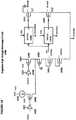
- Figure 2depicts an embodiment of an architecture for a flash memory system comprising die 200.
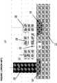
- Die 200comprises: memory array 215 and memory array 220 for storing data, memory arrays 215 and 220 comprising rows and columns of memory cells of the type described previously as memory cell 10 in Figure 1 , pad 240 and pad 280 for enabling electrical communication between the other components of die 200 and, typically, wire bonds (not shown) that in turn connect to pins (not shown) or package bumps that are used to access the integrated circuit from outside of the packaged chip or macro interface pins (not shown) for interconnecting to other macros on a SOC (system on chip); high voltage circuit 275 used to provide positive and negative voltage supplies for the system; control logic 270 for providing various control functions, such as redundancy and built-in self-testing; analog circuit 265; sensing circuits 260 and 261 used to read data from memory array 215 and memory array 220, respectively; row decoder circuit 245 and row decoder circuit 246 used to access the row in memory array 215 and memory
- the logic circuit 270In response to the read, erase or program command, the logic circuit 270 causes the various voltages to be supplied in a timely and least disturb manner to the various portions of both the selected memory cell 10 and the unselected memory cells 10.
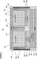
- the voltage and current appliedare as follows. As used hereinafter, the following abbreviations are used: source line or first region 14 (SL), bit line 20 (BL), word line 22 (WL), and coupling gate 26 (CG).
- the prior art method of performing read, erase, and program operations for selected memory cell 10 or unselected memory cell 10involves applying the following voltages:
- negative voltagescan be applied to word line 22 when memory cell 10 is unselected during read and program operations, such that the following voltages are applied:
- negative voltagescan be applied to word line 22 when memory cell 10 is unselected during read, erase, and program operations, and negative voltages can be applied to coupling gate 26 during an erase operation, such that the following voltages are applied:
- the CGINH signal listed aboveis a inhibit signal that is applied to the coupling gate 26 of an unselected cell that shares an erase gate 28 with a selected cell.
- Signals WL, BL, CG, SL, EG as corresponding respectively to terminals WL, BL, CG, SL, EG of the memory cell 10are as described above.
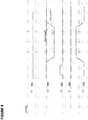
- a signal WL 302goes to high (e.g., ⁇ Vdd) first (such as to set a control signal in decoder circuit 1600 described below then start to settle down (to a bias voltage Vpwl).
- CG 306goes high after SL 308 (as shown by the dotted line waveform).
- Signal CGINH 312goes high, e.g., 3-6V, concurrently or at approximately the same time with the signal CG 306, and goes high preferably before signal EG 310 going high, e.g., 6-9V, to reduce the disturb effect on un-selected CG with CGINH level.
- the signal CGINH 312can go high at approximately the same time the signal EG 310.
- the signal WL 302settles down to a voltage Vpwl, e.g., 1v
- the signal BL 304settles down to a voltage Vdp, e.g., ⁇ 0.5v as CG goes high.
- Unselected WLsgoes down to 0V or negative, e.g., -0.5v, before or concurrent with selected WL 302 goes high.
- Unselected CGs and EGsstays at value in standby, e.g., 0 to 2.6v.
- Unselected SLsstays at a value in standby, e.g., 0v or switches to a bias voltage, e.g., 1v, as CG 306 goes high (unselected SL switching to a bias level to prevent leakage current through unselected cells through the BLs).
- the P substrate 12is at zero volts or alternatively can be at a negative voltage level in programming.
- the signal BL 304goes first high to Vinh (inhibit voltage) to prevent inadvertent program disturb due various signals are not settled yet during ramping to programming voltages.
- the timed sequence CG 306 vs. SL 310are optimized to reduce disturb effect, e.g. whichever signal causes more disturb goes high last.
- the ramping down of programming pulsesare reversed in order to minimize disturb (i.e., signal that goes up first now goes down last).
- the signal SL 310goes down, then CG 306 goes down, then WL 302 and BL 304 goes down. In the embodiment of programming with the substrate P going negative, e.g., -1V, this negative switching is concurrent with the signal WL goes low or the CG goes high.
- the timed sequence of EG 310 and CGINH 312is optimized to reduce disturb effect (soft erase in shared EG unselected row) as shown.
- the signal CGINH 312goes high before or approximately at the same time as the signal EG 312.
- the ramping downis reversed with CGINH 312 going down after or approximately at the same time as the signal EG 312.
- the signal WL 302goes high, e.g., Vdd, (such as to set control signal in the decoder circuit 1600 described below) then goes low, e.g., 0V (or alternatively a negative such as -0.5V).
- the signal CG 306goes negative, e.g., -6V to -9V.
- the selected EG 310then goes high, e.g., 9V to 6V.
- the signals BL 304, SL 308stays at a value in standby, e.g., 0V.
- Unselected WLsgoes down to 0V or negative, e.g., -0.5V, before or concurrent with selected EG 310 going high.
- Unselected CGs and EGsstay at value in standby, e.g., 0 to 2.6V.
- unselected CGscan be at a negative level (same as selected CG negative level).
- Unselected SLsstay at a value in standby, e.g., 0V.
- the P substrate 12is at zero volt or alternatively can be at a negative voltage level to enhance the erasing.
- the ramping down of erase pulsesis approximately reversed in order (i.e., signal that goes up first now goes down last).
- the signals EG 310 and CG 306goes to standby value, e.g., 0V.
- FIG. 5there is shown one example of signal timing waveforms for a read operation under Operation #3 described above.
- FIG 6there is shown one example of a signal timing waveform for read signals for positive/negative bias levels as described above for use in the memory device 10 of the present invention.
- This read signal waveformgoes with the program and erase signal waveform in Figure 3 for complete non-volatile erase/program/read operation.
- the SL 308is at standby value, e.g., 0V.
- the CG 306is at standby value, e.g., 0V or 2.6V, or alternatively switching to a higher bias value in read, e.g.
- the EG 310is at standby value, e.g., 0V or 2.6V, or alternatively switching to a higher bias value in read, e.g. 3.6V (to help increase the memory cell current due to EG voltage coupling to FG potential in read condition).
- the standby valuesare similar to those for program and erase condition.
- the WL 302 and BL 304switch to bias level in read, e.g. 2.6V and 1.0V respectively to selected memory cells for reading. Unselected WLs can be biased at zero volt or a negative voltage level, e.g., -0.5V (to reduce leakage on unselected rows).
- Unselected SLscan be biased at zero volt or a positive bias voltage level, e.g, 0.1-0.7V (to reduce leakage on unselected rows).
- Unselected BLscan be biased at zero volt or alternatively be floated, meaning no voltage applied (effectively reduce BL-BL capacitance in read).
- a Read Margin0 operationis performed after programming the whole array to detect weak programming cells.
- the cell currentis at a very low value normally ⁇ nano amperes (nA), this corresponds to reading out a '0' digital value (no cell current).
- nAnormal ⁇ nano amperes
- some cellsmay marginally stay at a couple micro amperes (due to weak programming due to various reasons such as cell leakage, weak cell programming coupling ratio, process geometrical effect, etc...) and this can causing read '0' to fail during the operating lifetime of the memory device 10.
- a Read Margin0is used to screen out those weak cells.
- the SL 308is at standby value, e.g., 0v.
- the WL 302 and BL 304switch to bias level in read, e.g. 2.6v and 1.0v respectively to selected memory cells for reading as in Read Normal condition.
- the CG 306is biased at a margin0 value in read, e.g. 3V, to detect weak programmed cells.
- the CG voltagewill couple into FG potential to amplify the weak programming effect, effectively increase the cell current, so the weak cells now read as a '1' instead of a '0' (effectively there is cell current instead of no cell current).
- a Read Margin 1 operationis performed after erasing the whole array to detect weak erased cells. Negative CG now is utilized to detect this condition.
- the SL 308is at standby value, e.g., 0v.
- the WL 302 and BL 304switch to bias level in read, e.g. 2.6v and 1.0v respectively to selected memory cells for reading as in Read Normal condition.
- the CG 306is biased at a margin1 value in read, e.g. -3v to -5v, to detect weak erased cells.
- the CG voltagewill couple negatively into FG potential to amplify the weak erased effect, effectively decrease the cell current (less FG potential), so the weak erased cells now read as a '0' instead of a '1' (effectively there is no cell current instead of cell current).
- FIG. 7Aan embodiment of a device cross section for memory cell 10 is depicted.
- Alternative embodiment of a device cross section for memory cell 10is in P-substrate 730 without High Voltage P-well 710 and Deep N-well 720.
- the memory cell 10 with source region 14, bitline region 16, channel region 18, and substrate region 12is shown sitting inside region High Voltage (HV) P-well 710 (other regions or terminals of the memory cell 10 is not shown).
- the region P-well 710sits inside a Deep N-well (DNW) region 720.
- the Deep N-well region 720sits inside a P-substrate 730. Due to isolation feature of the DNW region 720, typically connected to zero volt or Vdd, the HV P-well 710 can be biased negative to enhance electrical performance of the memory cells such as in erase or program.
- DNWDeep N-well
- the device cross section in Figure 7also is applicable for a high voltage nmos transistor in Deep N-well with high voltage nmos source, drain, and channel replacing respectively region 16, 14, 18 of the memory cell 10.
- Deep N-well 720similarly serves as a voltage isolation region such that the high voltage nmos can be applied in negative voltage operation. Embodiments are done to ensure reduced stress across transistor terminals and junctions of the HV nmos in DNW.
- FIG. 7Ba symbolic representation 740 of memory cell 10 is depicted, with deep N-well 720 shown as "DNW” and HV P-well 710 shown as P-well.” Shown in Figure 7B is a transistor symbol 750 for NMOS in HV P-well 710 inside Deep N-well 720.
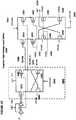
- negative high voltage level shifter 800which can be contained in logic 270, negative voltage driver circuit 230, high voltage driver circuit 225, and/or high voltage driver circuit 226 in Figure 2 .
- Negative high voltage level shifter 800receives an input, IN, and produces an output, VNBN. Negative high voltage level shifter 800 drives the deep N-well DNWB 804 of transistor 820 and transistor 830 to minimize the occurrence of a breakdown between layers of transistor 820 and transistor 830.
- DNW control circuit 835receives input IN2 802 to produce output DNWB 804 level as appropriate to reduce voltage stress for the transistors 820 and 830.
- Inverter 805receives an input, IN, and produces an inverter output, INB, which is input into inverter 810 and the gate of PMOS transistor 825. The output of inverter 810 is coupled to the gate of PMOS transistor 815.
- PMOS transistors 815 and 825are coupled to NMOS transistors 820 and 830 as shown.
- the output, VOUT 808,can vary between VHVNEG 806 and Vdd, which in this example are -8V and 2V, respectively.
- the DNWB levelcan be driven to -0.5V (without forward the P substrate - DNW junction) when VHVNEG is -8V to further minimize the voltage stress.
- the DNW control circuit 835can drive DNWB to be positive, e.g., Vdd level, to minimize noise or latch-up (preventing forwarding P substrate to Deep Nwell junction). This technique for driving DNWB is applicable for all of the embodiments to be described.
- negative high voltage level shifter 900which can be contained in logic 270, negative voltage driver circuit 230, high voltage driver circuit 225, and/or high voltage driver circuit 226 in Figure 2 .
- Negative high voltage level shifter 900comprises the same components as negative high voltage level shifter 800 with the addition of cascoding PMOS transistors 935 and 945 and cascoding NMOS transistors 940, and 950 as shown.
- Negative high voltage level shifter 900receives an input, IN, and generates an output, OUT 908.
- the output, OUT 908varies between VHVNEG 906 and Vdd, which in this example are -8V and 2V, respectively.
- the DNWB signal 904is driven similarly to that of the negative high voltage level shifter circuit 800 to minimize voltage stress.
- negative high voltage level shifter 1000which can be contained in logic 270, negative voltage driver circuit 230, high voltage driver circuit 225, and/or high voltage driver circuit 226 in Figure 2 .
- Negative high voltage level shifter 1000comprises the same components as negative high voltage level shifter 900 with the addition an intermediate (medium) negative level shifter 1002 consists of PMOS transistors 1075 and 1085 and NMOS transistors 1080 and 1090.
- the introduction of the intermediate negative level shifter 1002 with an intermediate negative level VHVNEGM, e.g., - 3V and additional intermediate negative bias level VNBP 1065 for gates of PMOS transistors and VNBN for gates of NMOS transistorsis to reduce voltage stress across the terminals of the PMOS and NMOS transistors in the negative (high) level shifter.
- Negative high voltage level shifter 1000receives an input, IN, and generates an output, OUT 1008.
- the output, OUT 1008,varies between VHVNEG 1006 , GND and Vdd, which in this example are -8V, 0V and 2V, respectively.
- VHVNEGMcan comprise a negative power supply of -3V.
- the output OUTM 1086 and OUTM_N 1076 of the intermediate negative level shifter 1002varies between VHVNEGM and Vdd, which in this example are -3V and 2V, respectively.
- VDDSWX 1012can be a switched supply that switches between 2V and 0V.
- VDDSWX (Vdd high supply)1012is initially at Vdd, e.g., 2V, and is switched to 0V when VHVNEG 1006 is at approximately half the maximum negative voltage, e.g., -4V, or at maximum negative voltage, e.g., -8V .
- the voltage VNBP 1065is at the intermediate negative voltage - 3V
- the voltage stress across gate-source/drain of the transistors 1035 and 1045is reduced.
- the voltage VNBN 1060is at the intermediate negative voltage -3V
- the voltage stress across gate-source/drain of the transistors 1040 and 1050is reduced and the voltage stress across source-drain of the transistors 1020 and 1030 is reduced.
- the voltage stress across gate-source/drain of the transistors 1020 and 1030is reduced and the voltage stress across source-drain of the transistors 1040 and 1050 is reduced.
- the cascoding PMOS transistors 1035 and 1045has its bulk (nwell) connected to its source to reduce voltage stress between the bulk and drain/source.
- the cascoding NMOS transistors 1040 and 1050has its bulk (Pwell) connected to its source to reduce voltage stress between the bulk and drain/source.
- Voltage supply circuit 1100comprises a first negative voltage level shifter circuit 1105 and a second negative voltage level shifter circuit 1110, each of which can comprise one of negative high voltage level shifters 800, 900, and 1000.
- first negative voltage level shifter circuit 1105 and second negative voltage level shifter circuit 1110together comprise negative high voltage level shifter 1000 and receives an input, IN, and generates a medium (intermediate) negative voltage, VHVNEGM, which ranges between 2V and -3V in this example, and a high negative voltage, VHVNEG, which ranges between 0V and -8V in this example.
- First negative voltage level shifter circuit 1105 and second negative voltage level shifter circuit 1110are coupled to NMOS transistor 1115 (cascoding transistor) and NMOS transistor 1120 as shown.
- DNWBreceives values of Vdd or 0V
- VPNext_pin 1101receives a voltage of 2V or -8V.
- the output of the circuit 1105 and 1110are for example equal to 2V which enable the NMOS transistors 1115 and 1120 to pass the VPNext_pin 1101 level into the VHVNEG 1106.
- the output of the circuit 1105 and 1110are for example equal to -3V and -8v respectively which disable the NMOS transistors 1115 and 1120.
- Voltage supply circuit 1200comprises negative voltage level shifter circuits 1225 and 1240, each of which comprises one of negative high voltage level shifters 800, 900, and 1000.
- Voltage supply circuit 1200receives an enable signal, EN_TXN, which is 0V in the "off' state and 2V in the "on” state, and generates a high negative voltage, VHVNEG, which ranges between 0V and -8V in this example.
- VNEG_3Vis 2V or -3V.
- Negative charge pump 1230 and 1235each pumps an input of -8V to an output of -12V.
- the outputs of the circuits 1230 and 1235is at for example -12V, hence enable the PMOS transistors 1215 and 1220 to pass the voltage from VPNext_pin level into the VHVNEG 1206.
- the outputs of the circuits 1230 and 1235is at for example 2V and 0V respectively, hence disable the PMOS transistors 1215 and 1220.
- the PMOS transistors 1210 and 1245serves as cascoding transistors to reduce voltage stress for the transistors 1205 and 1250 respectively.
- negative high voltage discharge circuit 1300is depicted.
- the transistors 1315 and 1325are enabled and outputs of circuit 1350 and 1355 are for example equal to Vdd (2V), VHVNEG is discharged through N2 from -8V to around -0.7V.
- the gates of NMOS transistors 1340 (cascoding transistor) and 1345equal to for example -3V and -8V in off state (the circuit 1350 and 1355 are disabled) to isolate the negative level VHVNEG from the NMOS transistor 1335.
- the discharge currentis controlled initially by current bias 1310 (enabled by the input IN1st) and then by the transistor 1325 (enabled by the input IN2nd).
- negative high voltage discharge circuit 1400is depicted.
- VHVNEGWhen the inputs, INlst and IN2nd, change state to enable, VHVNEG is discharged from -8V to an intermediate negative voltage level, determined by the number of Vt (threshold voltage) of diode connected NMOS transistors 1455 and 1460.
- the discharge currentis controlled initially by current bias 1435 (enabled by the input IN1st) and then by the transistor 1445 (enabled by the input IN2nd).
- VHVNEGis discharged quickly from the intermediate negative level through N1 1415 and N2 1420 transistor to around 0.0V.
- the gates of the NMOS transistors 1415 (cascoding transistor) and 1420are controlled by the medium negative level shifter 1405 and high negative level shifter 1410 respectively.
- Ground switch circuit 1500comprises negative high voltage circuit 1505, negative high voltage circuit 1510, NMOS transistor 1515, and NMOS transistor 1520.
- Ground switch circuit 1500receives an input signal, IN, and generates an output signal, VHVNEG.
- Decoder circuit 1600can be contained within logic 270, negative voltage driver circuit 230, high voltage driver circuit 225, and/or high voltage driver circuit 226 in Figure 2 .
- Decoder circuit 1600comprises high voltage level shifter 1605, negative high voltage level shifter 1610, high voltage decider enable circuit 1615, erase gate decoder 1620, control gate decoder 1625, and source line decoder 1630.
- High voltage enable circuit 1615is used to apply a high voltage from high voltage level shifter 1605 and/or a negative high voltage from negative high voltage level shifter 1610 to erase gate decoder 1620, coupling gate decoder 1625, and/or source line decoder 1630.
- Control gate decoder 1700comprises PMOS transistors 1705 and 1710, which provide a bias voltage VCGSUPR for the control gate during a read operation with current controlled by the PMOS transistor 1705, PMOS transistor 1725, which provides isolation for a negative high voltage, PMOS transistors 1715 and 1720, which provide a positive high voltage in program through PMOS transistors, and NMOS transistors 1730, 1735, 1740 and 1745 which can provide an inhibit voltage in program for the control gate and NMOS transistor 1750 and 1755 which together with the NMOS transistor 1730 can provide a negative high voltage in erase for the control gate.
- the NMOS transistor 1755serves as a current control for the negative voltage supply for the control gates.
- the NMOS transistor 1750is enabled by a negative voltage level shifter enabled by a local decoded sector enabling line SECHV_EN in erase.
- the circuit 1700provides decoding for four control gate CG [3:0], one erase gate EG, and one source line SL.
- PMOS transistors 1715with gates enabled by four global pre-decoded CG lines CGPH_HV_N[3:0].
- PMOS transistors 1710with gates enabled by a local decoded sector enabling line SECHV_EN.
- the PMOS transistor 1720is enabled by a local decoded sector enabling line SECHV_EN_N to pass positive high voltage VCGSUP into the control gates.
- the NMOS transistors 1735 and 1740are enabled by a global control signal CGN_ISO1 and CGN_ISO2 respectively to pass CG_LOW_BIAS (such as the inhibit voltage in program) or to serve as isolation voltage, e.g., -8V and -3V respectively.
- the NMOS transistor 1745is enabled by a local decoded sector enabling line SECHV_EN to pass CG_LOW_BIAS level into the control gate.
- DNWB 1704is controlled to be 0V when VHVNEG is at a negative voltage, e.g., -8V. As shown there is no cascoding transistor needed in the positive CG decoding function in the CG decoder 1700. Alternatively for negative CG decoding, the cascoding NMOS transistor 1740 is optional. Alternatively the current controlled NMOS transistor for negative CG decoding 1755 is optional
- Erase gate decoder 1800comprises PMOS transistors 1805 and 1810 and NMOS transistor 1815.
- the PMOS transistor 1810is a current controlled to pass a voltage or a high voltage VEGSUP into the erase gate.
- the PMOS transistor 1805is enabled by a local decoded sector enabling line EN_HV_N to pass voltage VEGSUP level into the erase gate.
- the NMOS transistor 1815is used to pass voltage EG_LOW_BIAS level, e.g, 0V-2.6V, into the erase gate.
- the decoded erase gateis shared across multiple rows of memory cells. As shown there is no cascoding transistor needed in the EG decoder 1620. Alternatively cascoding transistor PMOS and NMOS can be implemented for the EG decoder 1629.
- Source line decoder 1900comprises NMOS transistors 1905, 1910, 1915, and 1920.
- Source line decoder 1900provides a bias voltage, SLP_LOW_BIAS, at a value of around 0.5V for the source line for an unselected cell. Applying this bias voltage prevents leakage for unselected memory cells.
- the NMOS transistor 1915is used to pass VSLSUP level into the sourceline in program.
- the decoded sourcelineis shared across multiple rows of memory cells,
- the NMOS transistor 1920is used to monitor VSLMON level from the sourceline in program.
- the NMOS transistor 1905is used to pass SLRD_LOW_BIAS, e.g., 0V, level into the sourceline in read.
- High voltage negative chargepump circuit 2000comprises PMOS transistor 2005 and PMOS transistor 2010 coupled to negative pumped output, NMOS transistor 2015 and NMOS transistor 2020 coupled to positive pumped output, and pump stage circuits 2025, 2030, 2035, and 2040.
- High voltage negative chargepump circuit 2000provides a high negative voltage, VHV_NEG, and a high positive voltage, VHV_POS, which each of the pump stage circuits 2025, 2030, 2035, and 2045 receiving a voltage and outputting a higher positive voltage or a high negative voltage.
- the bulk (pwell) of the pass NMOS transistor of each stageis coupled to the output of the previous stage as shown.
- the DNWB of the NMOS transistorsare biased at 0V in negative voltage pumping , at HV in positive voltage pumping, and optionally at Vdd at other times.
- capacitorsthat can be used in chargepump circuit 2000 are depicted, including the use of PMOS transistor 2205, capacitor 2210, and NMOS transistor 2215.
- negative high voltage level shifter 2100is depicted.
- the components of negative high voltage level shifter 2100are identical to those of negative high voltage level shifter 1000 shown in Figure 10 , the difference being that the HV nwell (bulk of PMOS transistor) is driven by input inverters in Figure 21 is at 0V when the particular transistor is off, to minimize junction breakdown in the transistor.
- negative high voltage level shifter 2300receives an input, IN, and generates an output, OUT.
- OUTis -8V or 2V in this example.
- DNWBis driven by Vdd or 0V. In this circuit there are two PMOS in series but only single NMOS in each leg of the level shifter.
- multiplexing circuit 2400is depicted with only NMOS pass gate
- negative high voltage level shifter 2500is depicted.
- the components of negative high voltage level shifter 2100are identical to those of negative high voltage level shifter 900 shown in Figure 9 , the difference being the PMOS and NMOS transistors for cascoding purpose have its own separate bulk..
- the benefits of applying a negative voltage to the word line 22 or coupling gate 26 of the unselected or selected memory cells 10 during the operations of read, erase and programare to allow the memory cell to be scaled down more effectively.
- negative voltage on wordline of selected memory cellsallows overall erase voltage to be lowered thus allowing cell dimension to be smaller (sustaining less voltage across various inter-cell or inter-layer dimensional horizontal or vertical spacing, isolation, width, length, etc).
- negative voltage on wordline of unselected memory cellsreduces leakage for un-selected memory cells leading to less disturb (for un-selected cells in same sector), more accurate programming current (for selected cells, less leakage interference) and less power consumption.
- negative voltage on wordline of unselected memory cellsleads to more accurate sensing due to less interference from leakage. It is also advantageous to combine negative wordline, negative coupling gate and negative P substrate for use in memory array operation resulting in lowered erase/program voltages and current, more effective erasing and programming, less cell disturb, and less cell leakage.
Landscapes
- Engineering & Computer Science (AREA)
- Microelectronics & Electronic Packaging (AREA)
- Power Engineering (AREA)
- Read Only Memory (AREA)
- Non-Volatile Memory (AREA)
- Logic Circuits (AREA)
- Semiconductor Memories (AREA)
Description
- The present invention is defined in independent claim 1. The dependent claims define embodiments of the invention. A negative voltage is applied to the control gate and/or word line or a selected or unselected memory cell during the operations of read, program or erase.
- Non-volatile memory cells are well known in the art. One prior art non-volatile split
gate memory cell 10 is shown inFigure 1 . Thememory cell 10 comprises asemiconductor substrate 12 of a first conductivity type, such as P type. Thesubstrate 12 has a surface on which there is formed a first region 14 (also known as the source line SL) of a second conductivity type, such as N type. A second region 16 (also known as the drain line) also of N type is formed on the surface of thesubstrate 12. Between thefirst region 14 and thesecond region 16 is achannel region 18. Abit line BL 20 is connected to thesecond region 16. Aword line WL 22 is positioned above a first portion of thechannel region 18 and is insulated therefrom. Theword line 22 has little or no overlap with thesecond region 16. A floating gate FG 24 is over another portion of thechannel region 18. Thefloating gate 24 is insulated therefrom, and is adjacent to theword line 22. Thefloating gate 24 is also adjacent to thefirst region 14. Thefloating gate 24 may overlap thefirst region 14 to provide coupling from theregion 14 into thefloating gate 24. A coupling gate CG (also known as control gate) 26 is over thefloating gate 24 and is insulated therefrom. An erase gate EG 28 is over thefirst region 14 and is adjacent to thefloating gate 24 and the coupling gate 26 and is insulated therefrom. The top corner of thefloating gate 24 may point toward the inside corner of the T-shaped erase gate 28 to enhance erase efficiency. Theerase gate 28 is also insulated from thefirst region 14. Thecell 10 is more particularly described inUS7868375B . - One exemplary operation for erase and program of prior art non-volatile
memory cell 10 is as follows. Thecell 10 is erased, through a Fowler-Nordheim tunneling mechanism, by applying a high voltage on theerase gate 28 with other terminals equal to zero volt. Electrons tunnel from thefloating gate 24 into theerase gate 28 causing thefloating gate 24 to be positively charged, turning on thecell 10 in a read condition. The resulting cell erased state is known as '1' state. Thecell 10 is programmed, through a source side hot electron programming mechanism, by applying a high voltage on the coupling gate 26, a high voltage on thesource line 14, a medium voltage on theerase gate 28, and a programming current on thebit line 20. A portion of electrons flowing across the gap between theword line 22 and thefloating gate 24 acquire enough energy to inject into thefloating gate 24 causing thefloating gate 24 to be negatively charged, turning off the cell 1 0 in read condition. The resulting cell programmed state is known as '0' state. - In the prior art, various combinations of positive or zero voltages were applied to
word line 22, coupling gate 26, and floatinggate 24 to perform read, program, and erase operations. The prior art did not apply negative voltages for these operations. - Examples of prior art systems are found in
U.S. Patent Application Publication Nos. 2013/0242672 , and2002/0141249 andU.S. Patent 6,493,262 . Those prior art systems utilize conventional split-gate flash memory cells that do not fully utilize the range of possible operating voltages. - One object of the present invention is to utilize negative and positive voltages for a non-volatile memory cell device such that a negative voltage is applied to
word line 22 and/or coupling gate 26 during read, program, and/or erase operations for selected or unselected cells, depending on the operation. This will allow for the use of a lower positive voltage supply than in the prior art, which will allow for a more compact and space-efficient layout for the memory cell device. - The present invention utilizes negative and positive voltages for a non-volatile memory cell device such that a negative voltage is applied to
word line 22 and/or coupling gate 26 during read, program, and/or erase operations for selected or unselected cells, depending on the operation. As a result, the present invention allows for a more compact and space-efficient layout for the memory cell device than the prior art. Figure 1 is a cross-sectional view of a non-volatile memory cell of the prior art to which the method of the present invention can be applied.Figure 2 is a block diagram of a non-volatile memory device using the non-volatile memory cell of the prior art shown inFigure 1 .Figure 3 depicts exemplary waveforms for a programming operation of a non-volatile memory device.Figure 4 depicts exemplary waveforms for an erase operation of a non-volatile memory device.Figure 5 depicts exemplary waveforms for a normal read operation of a non-volatile memory device.Figure 6 depicts exemplary waveforms for a read operation of a non-volatile memory device using tolerance thresholds for reading a "0" and a "1."Figure 7A depicts a cross-section of a non-volatile memory cell.Figure 7B depicts a symbolic representation of the memory cell ofFigure 7A .Figure 7C depicts a symbolic representation of the memory cell ofFigure 7A .Figure 8 depicts a negative high voltage level shifter.Figure 9 depicts another negative high voltage level shifter.Figure 10 depicts another negative high voltage level shifter.Figure 11 depicts a voltage supply circuit.Figure 12 depicts another voltage supply circuit.Figure 13 depicts a negative high voltage discharge circuit.Figure 14 depicts another negative high voltage discharge circuit.Figure 15 depicts a ground switch.Figure 16 depicts a decoder circuit.Figure 17 depicts a coupling gate decoder circuit.Figure 18 depicts an erase gate decoder circuit.Figure 19 depicts a source line decoder circuit.Figure 20 depicts a charge pump.Figure 21 depicts a negative high voltage level shifter.Figures 22A, 22B, and 22C depict capacitors.Figure 23 depicts another negative high voltage level shifter.Figure 24 depicts a multiplexor.Figure 25 depicts another negative high voltage level shifter.Figure 2 depicts an embodiment of an architecture for a flash memorysystem comprising die 200. Die 200 comprises: memory array 215 and memory array 220 for storing data, memory arrays 215 and 220 comprising rows and columns of memory cells of the type described previously as memory cell 10 inFigure 1 , pad 240 and pad 280 for enabling electrical communication between the other components of die 200 and, typically, wire bonds (not shown) that in turn connect to pins (not shown) or package bumps that are used to access the integrated circuit from outside of the packaged chip or macro interface pins (not shown) for interconnecting to other macros on a SOC (system on chip); high voltage circuit 275 used to provide positive and negative voltage supplies for the system; control logic 270 for providing various control functions, such as redundancy and built-in self-testing; analog circuit 265; sensing circuits 260 and 261 used to read data from memory array 215 and memory array 220, respectively; row decoder circuit 245 and row decoder circuit 246 used to access the row in memory array 215 and memory array 220, respectively, to be read from or written to; column decoder circuit 255 and column decoder circuit 256 used to access bytes in memory array 215 and memory array 220, respectively, to be read from or written to; charge pump circuit 250 and charge pump circuit 251, used to provide increased voltages for program and erase operations for memory array 215 and memory array 220, respectively; negative voltage driver circuit 230 shared by memory array 215 and memory array 220 for read and write operations; high voltage driver circuit 225 used by memory array 215 during read and write operations and high voltage driver circuit 226 used by memory array 220 during read and write operations.- In response to the read, erase or program command, the
logic circuit 270 causes the various voltages to be supplied in a timely and least disturb manner to the various portions of both the selectedmemory cell 10 and theunselected memory cells 10. - For the selected and unselected
memory cell 10, the voltage and current applied are as follows. As used hereinafter, the following abbreviations are used: source line or first region 14 (SL), bit line 20 (BL), word line 22 (WL), and coupling gate 26 (CG). - The prior art method of performing read, erase, and program operations for selected
memory cell 10 or unselectedmemory cell 10 involves applying the following voltages: 
- In one embodiment, negative voltages can be applied to
word line 22 whenmemory cell 10 is unselected during read and program operations, such that the following voltages are applied: 
- In another embodiment, negative voltages can be applied to
word line 22 whenmemory cell 10 is unselected during read, erase, and program operations, and negative voltages can be applied to coupling gate 26 during an erase operation, such that the following voltages are applied: 

- The CGINH signal listed above is a inhibit signal that is applied to the coupling gate 26 of an unselected cell that shares an erase
gate 28 with a selected cell. - Referring to
Figure 3 , there is shown one example of signal timing waveforms for a program operation underOperation # 3 described above. Signals WL, BL, CG, SL, EG as corresponding respectively to terminals WL, BL, CG, SL, EG of thememory cell 10 are as described above. For programming, asignal WL 302 goes to high (e.g.,∼ Vdd) first (such as to set a control signal indecoder circuit 1600 described below then start to settle down (to a bias voltage Vpwl). Then signalBL 304 andCG 306 go high, e.g., ∼Vinh =∼ Vdd and 10 to 11v respectively, and thenSL 308 goes high (e.g., ∼ 4.5v to 5v) . Alternatively,CG 306 goes high after SL 308 (as shown by the dotted line waveform).Signal CGINH 312 goes high, e.g., 3-6V, concurrently or at approximately the same time with thesignal CG 306, and goes high preferably beforesignal EG 310 going high, e.g., 6-9V, to reduce the disturb effect on un-selected CG with CGINH level. Alternatively, thesignal CGINH 312 can go high at approximately the same time thesignal EG 310. Thesignal WL 302 settles down to a voltage Vpwl, e.g., 1v, and thesignal BL 304 settles down to a voltage Vdp, e.g., ∼0.5v as CG goes high. Unselected WLs goes down to 0V or negative, e.g., -0.5v, before or concurrent with selectedWL 302 goes high. Unselected CGs and EGs stays at value in standby, e.g., 0 to 2.6v. Unselected SLs stays at a value in standby, e.g., 0v or switches to a bias voltage, e.g., 1v, asCG 306 goes high (unselected SL switching to a bias level to prevent leakage current through unselected cells through the BLs). TheP substrate 12 is at zero volts or alternatively can be at a negative voltage level in programming. - The
signal BL 304 goes first high to Vinh (inhibit voltage) to prevent inadvertent program disturb due various signals are not settled yet during ramping to programming voltages. Thetimed sequence CG 306vs. SL 310 are optimized to reduce disturb effect, e.g. whichever signal causes more disturb goes high last. The ramping down of programming pulses are reversed in order to minimize disturb (i.e., signal that goes up first now goes down last). Thesignal SL 310 goes down, thenCG 306 goes down, thenWL 302 andBL 304 goes down. In the embodiment of programming with the substrate P going negative, e.g., -1V, this negative switching is concurrent with the signal WL goes low or the CG goes high. The timed sequence ofEG 310 andCGINH 312 is optimized to reduce disturb effect (soft erase in shared EG unselected row) as shown. Thesignal CGINH 312 goes high before or approximately at the same time as thesignal EG 312. The ramping down is reversed withCGINH 312 going down after or approximately at the same time as thesignal EG 312. - Referring to
Figure 4 , there is shown one example of signal timing waveforms for an erase operation underOperation # 3 described above. For erase, thesignal WL 302 goes high, e.g., Vdd, (such as to set control signal in thedecoder circuit 1600 described below) then goes low, e.g., 0V (or alternatively a negative such as -0.5V). At approximately same time or a short time thereafter as theWL 302 going low, thesignal CG 306 goes negative, e.g., -6V to -9V. The selectedEG 310 then goes high, e.g., 9V to 6V. Thesignals BL 304,SL 308 stays at a value in standby, e.g., 0V. Unselected WLs goes down to 0V or negative, e.g., -0.5V, before or concurrent with selectedEG 310 going high. Unselected CGs and EGs stay at value in standby, e.g., 0 to 2.6V. Alternatively unselected CGs can be at a negative level (same as selected CG negative level). Unselected SLs stay at a value in standby, e.g., 0V. TheP substrate 12 is at zero volt or alternatively can be at a negative voltage level to enhance the erasing. - The ramping down of erase pulses is approximately reversed in order (i.e., signal that goes up first now goes down last). The signals EG 310 and
CG 306 goes to standby value, e.g., 0V. - Referring to
Figure 5 , there is shown one example of signal timing waveforms for a read operation underOperation # 3 described above. Referring toFigure 6 , there is shown one example of a signal timing waveform for read signals for positive/negative bias levels as described above for use in thememory device 10 of the present invention. This read signal waveform goes with the program and erase signal waveform inFigure 3 for complete non-volatile erase/program/read operation. For Read Normal waveform, theSL 308 is at standby value, e.g., 0V. TheCG 306 is at standby value, e.g., 0V or 2.6V, or alternatively switching to a higher bias value in read, e.g. 3.6V (to help increase the memory cell current due to CG voltage coupling to FG potential in read condition). TheEG 310 is at standby value, e.g., 0V or 2.6V, or alternatively switching to a higher bias value in read, e.g. 3.6V (to help increase the memory cell current due to EG voltage coupling to FG potential in read condition). The standby values are similar to those for program and erase condition. TheWL 302 andBL 304 switch to bias level in read, e.g. 2.6V and 1.0V respectively to selected memory cells for reading. Unselected WLs can be biased at zero volt or a negative voltage level, e.g., -0.5V (to reduce leakage on unselected rows). Unselected SLs can be biased at zero volt or a positive bias voltage level, e.g, 0.1-0.7V (to reduce leakage on unselected rows). Unselected BLs can be biased at zero volt or alternatively be floated, meaning no voltage applied (effectively reduce BL-BL capacitance in read). - With reference to
Figure 6 , a Read Margin0 operation is performed after programming the whole array to detect weak programming cells. After programming, the cell current is at a very low value normally <nano amperes (nA), this corresponds to reading out a '0' digital value (no cell current). However some cells may marginally stay at a couple micro amperes (due to weak programming due to various reasons such as cell leakage, weak cell programming coupling ratio, process geometrical effect, etc...) and this can causing read '0' to fail during the operating lifetime of thememory device 10. A Read Margin0 is used to screen out those weak cells. For Read Margin0 waveform, theSL 308 is at standby value, e.g., 0v. TheWL 302 andBL 304 switch to bias level in read, e.g. 2.6v and 1.0v respectively to selected memory cells for reading as in Read Normal condition. TheCG 306 is biased at a margin0 value in read, e.g. 3V, to detect weak programmed cells. The CG voltage will couple into FG potential to amplify the weak programming effect, effectively increase the cell current, so the weak cells now read as a '1' instead of a '0' (effectively there is cell current instead of no cell current). - A Read Margin 1 operation is performed after erasing the whole array to detect weak erased cells. Negative CG now is utilized to detect this condition. The
SL 308 is at standby value, e.g., 0v. TheWL 302 andBL 304 switch to bias level in read, e.g. 2.6v and 1.0v respectively to selected memory cells for reading as in Read Normal condition. TheCG 306 is biased at a margin1 value in read, e.g. -3v to -5v, to detect weak erased cells. The CG voltage will couple negatively into FG potential to amplify the weak erased effect, effectively decrease the cell current (less FG potential), so the weak erased cells now read as a '0' instead of a '1' (effectively there is no cell current instead of cell current). - Referring to
Figure 7A , an embodiment of a device cross section formemory cell 10 is depicted. Alternative embodiment of a device cross section formemory cell 10 is in P-substrate 730 without High Voltage P-well 710 and Deep N-well 720. Thememory cell 10 withsource region 14,bitline region 16,channel region 18, andsubstrate region 12 is shown sitting inside region High Voltage (HV) P-well 710 (other regions or terminals of thememory cell 10 is not shown). The region P-well 710 sits inside a Deep N-well (DNW)region 720. The Deep N-well region 720 sits inside a P-substrate 730. Due to isolation feature of theDNW region 720, typically connected to zero volt or Vdd, the HV P-well 710 can be biased negative to enhance electrical performance of the memory cells such as in erase or program. - The device cross section in
Figure 7 also is applicable for a high voltage nmos transistor in Deep N-well with high voltage nmos source, drain, and channel replacing respectivelyregion memory cell 10. Deep N-well 720 similarly serves as a voltage isolation region such that the high voltage nmos can be applied in negative voltage operation. Embodiments are done to ensure reduced stress across transistor terminals and junctions of the HV nmos in DNW. - Referring to
Figure 7B , asymbolic representation 740 ofmemory cell 10 is depicted, with deep N-well 720 shown as "DNW" and HV P-well 710 shown as
P-well." Shown inFigure 7B is atransistor symbol 750 for NMOS in HV P-well 710 inside Deep N-well 720. - Referring to
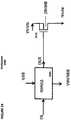
Figure 8 , a first embodiment of a level shifter is depicted, negative highvoltage level shifter 800, which can be contained inlogic 270, negativevoltage driver circuit 230, highvoltage driver circuit 225, and/or highvoltage driver circuit 226 inFigure 2 . - Negative high
voltage level shifter 800 receives an input, IN, and produces an output, VNBN. Negative highvoltage level shifter 800 drives the deep N-well DNWB 804 oftransistor 820 andtransistor 830 to minimize the occurrence of a breakdown between layers oftransistor 820 andtransistor 830.DNW control circuit 835 receivesinput IN2 802 to produceoutput DNWB 804 level as appropriate to reduce voltage stress for thetransistors Inverter 805 receives an input, IN, and produces an inverter output, INB, which is input intoinverter 810 and the gate ofPMOS transistor 825. The output ofinverter 810 is coupled to the gate ofPMOS transistor 815.PMOS transistors NMOS transistors VOUT 808, can vary betweenVHVNEG 806 and Vdd, which in this example are -8V and 2V, respectively. The DNWB level for example can be from 0V to Vdd (e.g., 2.5V) and it is 0V when VHVNEG is -8V. This minimizes the voltage stress to 8V (instead of 8V+2.5V= 10.5V) between DNWB and HV P-well and source/drain of thetransistors DNW control circuit 835 can drive DNWB to be positive, e.g., Vdd level, to minimize noise or latch-up (preventing forwarding P substrate to Deep Nwell junction). This technique for driving DNWB is applicable for all of the embodiments to be described. - Referring to
Figure 9 , a second embodiment of a level shifter is depicted, negative highvoltage level shifter 900, which can be contained inlogic 270, negativevoltage driver circuit 230, highvoltage driver circuit 225, and/or highvoltage driver circuit 226 inFigure 2 . Negative highvoltage level shifter 900 comprises the same components as negative highvoltage level shifter 800 with the addition ofcascoding PMOS transistors cascoding NMOS transistors voltage level shifter 900 receives an input, IN, and generates an output,OUT 908. The output,OUT 908, varies betweenVHVNEG 906 and Vdd, which in this example are -8V and 2V, respectively. TheDNWB signal 904 is driven similarly to that of the negative high voltagelevel shifter circuit 800 to minimize voltage stress. The gates of thePMOS transistors NMOS transistors - Referring to
Figure 10 , a third embodiment of a level shifter is depicted, negative highvoltage level shifter 1000, which can be contained inlogic 270, negativevoltage driver circuit 230, highvoltage driver circuit 225, and/or highvoltage driver circuit 226 inFigure 2 . Negative highvoltage level shifter 1000 comprises the same components as negative highvoltage level shifter 900 with the addition an intermediate (medium)negative level shifter 1002 consists ofPMOS transistors NMOS transistors negative level shifter 1002 with an intermediate negative level VHVNEGM, e.g., - 3V and additional intermediate negativebias level VNBP 1065 for gates of PMOS transistors and VNBN for gates of NMOS transistors is to reduce voltage stress across the terminals of the PMOS and NMOS transistors in the negative (high) level shifter. Negative highvoltage level shifter 1000 receives an input, IN, and generates an output, OUT 1008. The output, OUT 1008, varies betweenVHVNEG 1006 , GND and Vdd, which in this example are -8V, 0V and 2V, respectively. The output, OUT 1008, varies betweenVHVNEG 1006 , and GND (=VDDSWX 1012), which in this example are -8V and 0V, respectively when thevoltage VHVNEG 1006 is at maximum high negative voltage -8V. VHVNEGM can comprise a negative power supply of -3V. Theoutput OUTM 1086 and OUTM_N 1076 of the intermediatenegative level shifter 1002 varies between VHVNEGM and Vdd, which in this example are -3V and 2V, respectively.VDDSWX 1012 can be a switched supply that switches between 2V and 0V. VDDSWX (Vdd high supply)1012 is initially at Vdd, e.g., 2V, and is switched to 0V whenVHVNEG 1006 is at approximately half the maximum negative voltage, e.g., -4V, or at maximum negative voltage, e.g., -8V .VNBP 1065 can be switched between 0V and -3V. When theVDDSWX 1012 is at 0V, theVNBP 1065 is at -3V, the output OUTM_N 1076 is at -3V (=VHVNEGM) to pass 0V to theoutput OUT 1008. Since thevoltage VNBP 1065 is at the intermediate negative voltage - 3V, the voltage stress across gate-source/drain of thetransistors voltage VNBN 1060 is at the intermediate negative voltage -3V, the voltage stress across gate-source/drain of thetransistors transistors transistors transistors cascoding PMOS transistors cascoding NMOS transistors - Referring to
Figure 11 ,voltage supply circuit 1100 is depicted.Voltage supply circuit 1100 comprises a first negative voltagelevel shifter circuit 1105 and a second negative voltagelevel shifter circuit 1110, each of which can comprise one of negative highvoltage level shifters level shifter circuit 1105 and second negative voltagelevel shifter circuit 1110 together comprise negative highvoltage level shifter 1000 and receives an input, IN, and generates a medium (intermediate) negative voltage, VHVNEGM, which ranges between 2V and -3V in this example, and a high negative voltage, VHVNEG, which ranges between 0V and -8V in this example. First negative voltagelevel shifter circuit 1105 and second negative voltagelevel shifter circuit 1110 are coupled to NMOS transistor 1115 (cascoding transistor) andNMOS transistor 1120 as shown. DNWB receives values of Vdd or 0V, andVPNext_pin 1101 receives a voltage of 2V or -8V. When thecircuit 1100 is enabled, the output of thecircuit NMOS transistors VPNext_pin 1101 level into theVHVNEG 1106. When thecircuit 1100 is disabled, the output of thecircuit NMOS transistors - Referring to
Figure 12 ,voltage supply circuit 1200 is depicted.Voltage supply circuit 1100 comprises negative voltagelevel shifter circuits voltage level shifters Voltage supply circuit 1200 receives an enable signal, EN_TXN, which is 0V in the "off' state and 2V in the "on" state, and generates a high negative voltage, VHVNEG, which ranges between 0V and -8V in this example. VNEG_3V is 2V or -3V.Negative charge pump circuit 1200 is enabled, the outputs of thecircuits PMOS transistors VHVNEG 1206. When thecircuit 1200 is disabled, the outputs of thecircuits PMOS transistors PMOS transistors transistors - Referring to
Figure 13 , negative highvoltage discharge circuit 1300 is depicted. When the inputs, IN3, INlst and IN2nd, change state to enable, thetransistors circuit circuit NMOS transistor 1335. The discharge current is controlled initially by current bias 1310 (enabled by the input IN1st) and then by the transistor 1325 (enabled by the input IN2nd). - Referring to
Figure 14 , negative highvoltage discharge circuit 1400 is depicted. When the inputs, INlst and IN2nd, change state to enable, VHVNEG is discharged from -8V to an intermediate negative voltage level, determined by the number of Vt (threshold voltage) of diode connectedNMOS transistors N1 1415 andN2 1420 transistor to around 0.0V. The gates of the NMOS transistors 1415 (cascoding transistor) and 1420 are controlled by the mediumnegative level shifter 1405 and highnegative level shifter 1410 respectively. - Referring to
Figure 15 ,ground switch circuit 1500 is depicted.Ground switch circuit 1500 comprises negativehigh voltage circuit 1505, negativehigh voltage circuit 1510,NMOS transistor 1515, andNMOS transistor 1520.Ground switch circuit 1500 receives an input signal, IN, and generates an output signal, VHVNEG. - Referring to
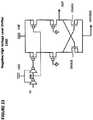
Figure 16 ,decoder circuit 1600 is depicted.Decoder circuit 1600 can be contained withinlogic 270, negativevoltage driver circuit 230, highvoltage driver circuit 225, and/or highvoltage driver circuit 226 inFigure 2 .Decoder circuit 1600 comprises highvoltage level shifter 1605, negative highvoltage level shifter 1610, high voltage decider enablecircuit 1615, erasegate decoder 1620,control gate decoder 1625, andsource line decoder 1630. High voltage enablecircuit 1615 is used to apply a high voltage from highvoltage level shifter 1605 and/or a negative high voltage from negative highvoltage level shifter 1610 to erasegate decoder 1620,coupling gate decoder 1625, and/orsource line decoder 1630. - Referring to
Figure 17 , anembodiment 1700 is shown forcontrol gate decoder 1625.Control gate decoder 1700 comprisesPMOS transistors PMOS transistor 1705,PMOS transistor 1725, which provides isolation for a negative high voltage,PMOS transistors NMOS transistors NMOS transistor NMOS transistor 1730 can provide a negative high voltage in erase for the control gate. TheNMOS transistor 1755 serves as a current control for the negative voltage supply for the control gates. TheNMOS transistor 1750 is enabled by a negative voltage level shifter enabled by a local decoded sector enabling line SECHV_EN in erase. As shown thecircuit 1700 provides decoding for four control gate CG [3:0], one erase gate EG, and one source line SL. There are fourPMOS transistors 1715 with gates enabled by four global pre-decoded CG lines CGPH_HV_N[3:0]. There are fourPMOS transistors 1710 with gates enabled by a local decoded sector enabling line SECHV_EN. There are fourisolation PMOS transistors 1725 with gates enabled by a ground line. There are fourNMOS transistors 1730 with gates enabled by four global pre-decoded CG lines CGNH_HV_N [3:0]. ThePMOS transistor 1720 is enabled by a local decoded sector enabling line SECHV_EN_N to pass positive high voltage VCGSUP into the control gates. TheNMOS transistors 1735 and 1740 are enabled by a global control signal CGN_ISO1 and CGN_ISO2 respectively to pass CG_LOW_BIAS (such as the inhibit voltage in program) or to serve as isolation voltage, e.g., -8V and -3V respectively. TheNMOS transistor 1745 is enabled by a local decoded sector enabling line SECHV_EN to pass CG_LOW_BIAS level into the control gate.DNWB 1704 is controlled to be 0V when VHVNEG is at a negative voltage, e.g., -8V. As shown there is no cascoding transistor needed in the positive CG decoding function in theCG decoder 1700. Alternatively for negative CG decoding, thecascoding NMOS transistor 1740 is optional. Alternatively the current controlled NMOS transistor fornegative CG decoding 1755 is optional - Referring to
Figure 18 , anembodiment 1800 is shown for erasegate decoder 1620. Erasegate decoder 1800 comprisesPMOS transistors NMOS transistor 1815. ThePMOS transistor 1810 is a current controlled to pass a voltage or a high voltage VEGSUP into the erase gate. ThePMOS transistor 1805 is enabled by a local decoded sector enabling line EN_HV_N to pass voltage VEGSUP level into the erase gate. TheNMOS transistor 1815 is used to pass voltage EG_LOW_BIAS level, e.g, 0V-2.6V, into the erase gate. The decoded erase gate is shared across multiple rows of memory cells. As shown there is no cascoding transistor needed in theEG decoder 1620. Alternatively cascoding transistor PMOS and NMOS can be implemented for the EG decoder 1629. - Referring to
Figure 19 , anembodiment 1900 is shown forsource line decoder 1630.Source line decoder 1900 comprisesNMOS transistors Source line decoder 1900 provides a bias voltage, SLP_LOW_BIAS, at a value of around 0.5V for the source line for an unselected cell. Applying this bias voltage prevents leakage for unselected memory cells. TheNMOS transistor 1915 is used to pass VSLSUP level into the sourceline in program. The decoded sourceline is shared across multiple rows of memory cells, TheNMOS transistor 1920 is used to monitor VSLMON level from the sourceline in program. TheNMOS transistor 1905 is used to pass SLRD_LOW_BIAS, e.g., 0V, level into the sourceline in read. - Referring to
Figure 20 , high voltagenegative chargepump circuit 2000 is depicted. High voltagenegative chargepump circuit 2000 comprisesPMOS transistor 2005 andPMOS transistor 2010 coupled to negative pumped output,NMOS transistor 2015 andNMOS transistor 2020 coupled to positive pumped output, and pumpstage circuits negative chargepump circuit 2000 provides a high negative voltage, VHV_NEG, and a high positive voltage, VHV_POS, which each of thepump stage circuits - Referring to
Figures 22A, 22B, and 22C , examples of capacitors that can be used inchargepump circuit 2000 are depicted, including the use ofPMOS transistor 2205,capacitor 2210, andNMOS transistor 2215. - Referring to
Figure 21 , negative highvoltage level shifter 2100 is depicted. The components of negative highvoltage level shifter 2100 are identical to those of negative highvoltage level shifter 1000 shown inFigure 10 , the difference being that the HV nwell (bulk of PMOS transistor) is driven by input inverters inFigure 21 is at 0V when the particular transistor is off, to minimize junction breakdown in the transistor. - Referring to
Figure 23 , negative highvoltage level shifter 2300 is depicted. Negative highvoltage level shifter 2300 receives an input, IN, and generates an output, OUT. OUT is -8V or 2V in this example. DNWB is driven by Vdd or 0V. In this circuit there are two PMOS in series but only single NMOS in each leg of the level shifter. - Referring to
Figure 24 ,multiplexing circuit 2400 is depicted with only NMOS pass gate - Referring to
Figure 25 , negative highvoltage level shifter 2500 is depicted. The components of negative highvoltage level shifter 2100 are identical to those of negative highvoltage level shifter 900 shown inFigure 9 , the difference being the PMOS and NMOS transistors for cascoding purpose have its own separate bulk..
The benefits of applying a negative voltage to theword line 22 or coupling gate 26 of the unselected or selectedmemory cells 10 during the operations of read, erase and program are to allow the memory cell to be scaled down more effectively. During erase, negative voltage on wordline of selected memory cells allows overall erase voltage to be lowered thus allowing cell dimension to be smaller (sustaining less voltage across various inter-cell or inter-layer dimensional horizontal or vertical spacing, isolation, width, length, etc...). During program, negative voltage on wordline of unselected memory cells reduces leakage for un-selected memory cells leading to less disturb (for un-selected cells in same sector), more accurate programming current (for selected cells, less leakage interference) and less power consumption. For read, negative voltage on wordline of unselected memory cells leads to more accurate sensing due to less interference from leakage. It is also advantageous to combine negative wordline, negative coupling gate and negative P substrate for use in memory array operation resulting in lowered erase/program voltages and current, more effective erasing and programming, less cell disturb, and less cell leakage.


Claims (5)
- A negative high voltage level shifter (1000, 2100) for receiving an input and generating a first negative voltage applied to a split-gate flash memory cell, the negative high voltage level shifter comprising:a cascode circuit comprising a first PMOS transistor (1025) coupled in series to a second PMOS transistor (1045) and a first NMOS transistor (1050) coupled in series to a second NMOS transistor (1030), the first NMOS transistor comprising a deep N-well, the second NMOS transistor comprising a deep N-well;a negative medium voltage level shifter circuit (1002, 1105, 1110, 1405) for generating a second negative voltage used to control the gate of the second PMOS transistor and the gate of the first NMOS transistor;wherein the first negative voltage_is generated as the output (1008) at the node between the first NMOS transistor and second PMOS transistor in response to the input having a low value.
- The negative high voltage level shifter of claim 1, wherein the deep N-wells are driven to zero voltage when the output generates a high negative voltage.
- The negative high voltage level shifter of claim 1, wherein a Vdd high voltage supply switches to ground when an output of the negative high voltage level shifter generates a negative voltage.
- The negative high voltage level shifter of claim 1, wherein the first negative voltage is applied to a coupling gate of a selected memory cell during an erase operation and the second negative voltage is applied to word line terminals of unselected memory cells during an erase, read, or program operation.
- The negative high voltage level shifter of claim 1, wherein the first negative voltage is between -5 and -9 volts.
Priority Applications (1)
| Application Number | Priority Date | Filing Date | Title |
|---|---|---|---|
| EP19203643.2AEP3629331B1 (en) | 2015-01-21 | 2015-12-04 | Split gate flash memory system using complementary voltage supplies |
Applications Claiming Priority (2)
| Application Number | Priority Date | Filing Date | Title |
|---|---|---|---|
| US14/602,262US9361995B1 (en) | 2015-01-21 | 2015-01-21 | Flash memory system using complementary voltage supplies |
| PCT/US2015/064082WO2016118238A1 (en) | 2015-01-21 | 2015-12-04 | Split gate flash memory system using complementary voltage supplies |
Related Child Applications (2)
| Application Number | Title | Priority Date | Filing Date |
|---|---|---|---|
| EP19203643.2ADivisionEP3629331B1 (en) | 2015-01-21 | 2015-12-04 | Split gate flash memory system using complementary voltage supplies |
| EP19203643.2ADivision-IntoEP3629331B1 (en) | 2015-01-21 | 2015-12-04 | Split gate flash memory system using complementary voltage supplies |
Publications (2)
| Publication Number | Publication Date |
|---|---|
| EP3248193A1 EP3248193A1 (en) | 2017-11-29 |
| EP3248193B1true EP3248193B1 (en) | 2020-02-05 |
Family
ID=54884436
Family Applications (2)
| Application Number | Title | Priority Date | Filing Date |
|---|---|---|---|
| EP19203643.2AActiveEP3629331B1 (en) | 2015-01-21 | 2015-12-04 | Split gate flash memory system using complementary voltage supplies |
| EP15813222.5AActiveEP3248193B1 (en) | 2015-01-21 | 2015-12-04 | Split gate flash memory system using complementary voltage supplies |
Family Applications Before (1)
| Application Number | Title | Priority Date | Filing Date |
|---|---|---|---|
| EP19203643.2AActiveEP3629331B1 (en) | 2015-01-21 | 2015-12-04 | Split gate flash memory system using complementary voltage supplies |
Country Status (7)
| Country | Link |
|---|---|
| US (4) | US9361995B1 (en) |
| EP (2) | EP3629331B1 (en) |
| JP (2) | JP2018504731A (en) |
| KR (2) | KR20170106442A (en) |
| CN (3) | CN113241101B (en) |
| TW (2) | TWI587305B (en) |
| WO (1) | WO2016118238A1 (en) |
Families Citing this family (24)
| Publication number | Priority date | Publication date | Assignee | Title |
|---|---|---|---|---|
| US9953719B2 (en) | 2016-05-18 | 2018-04-24 | Silicon Storage Technology, Inc. | Flash memory cell and associated decoders |
| US9911501B2 (en) | 2016-05-24 | 2018-03-06 | Silicon Storage Technology, Inc. | Sensing amplifier comprising a built-in sensing offset for flash memory devices |
| US10684669B1 (en)* | 2017-07-28 | 2020-06-16 | Maxim Integrated Products, Inc. | Logic level shifter interface between power domains |
| CN109417606B (en)* | 2017-08-17 | 2021-10-26 | 深圳市汇顶科技股份有限公司 | Level converter capable of outputting positive and negative voltages |
| US10796763B2 (en) | 2018-01-26 | 2020-10-06 | Stmicroelectronics (Rousset) Sas | Method for programming a split-gate memory cell and corresponding memory device |
| US10910061B2 (en)* | 2018-03-14 | 2021-02-02 | Silicon Storage Technology, Inc. | Method and apparatus for programming analog neural memory in a deep learning artificial neural network |
| CN108648777B (en)* | 2018-05-10 | 2020-08-11 | 上海华虹宏力半导体制造有限公司 | Programming sequential circuit and method of double-separation gate flash memory |
| US10847225B2 (en)* | 2018-06-20 | 2020-11-24 | Microchip Technology Incorporated | Split-gate flash memory cell with improved read performance |
| US10991426B2 (en) | 2019-01-25 | 2021-04-27 | Taiwan Semiconductor Manufacturing Company, Ltd. | Memory device current limiter |
| DE102019132067A1 (en) | 2019-01-25 | 2020-07-30 | Taiwan Semiconductor Manufacturing Co., Ltd. | CURRENT LIMITER FOR STORAGE DEVICE |
| CN111916432B (en)* | 2019-05-08 | 2022-09-09 | 深圳第三代半导体研究院 | A uniformly luminous front-mounted integrated unit diode chip |
| US11070208B2 (en)* | 2019-09-17 | 2021-07-20 | Taiwan Semiconductor Manufacturing Company, Ltd. | Level shifter |
| US11532354B2 (en) | 2020-03-22 | 2022-12-20 | Silicon Storage Technology, Inc. | Precision tuning of a page or word of non-volatile memory cells and associated high voltage circuits for an analog neural memory array in an artificial neural network |
| FR3113976B1 (en) | 2020-09-07 | 2023-07-28 | St Microelectronics Rousset | Electrically programmable and erasable ROM type memory |
| KR102789800B1 (en) | 2020-09-16 | 2025-04-01 | 삼성전자주식회사 | Negative level shifter and nonvolatile memory device including the same |
| CN112185447B (en)* | 2020-09-29 | 2023-08-01 | 中科南京智能技术研究院 | 8-pipe double-split control storage unit, storage array and in-memory computing device |
| CN114822657A (en)* | 2020-12-21 | 2022-07-29 | 长江存储科技有限责任公司 | Control method of deep well voltage of semiconductor device |
| JP7701988B2 (en)* | 2021-05-18 | 2025-07-02 | シリコン ストーリッジ テクノロージー インコーポレイテッド | Non-volatile memory cell array formed in a P-well in a deep N-well in a P-substrate |
| US11405039B1 (en) | 2021-06-02 | 2022-08-02 | Sandisk Technologies Llc | Level shifter with improved negative voltage capability |
| US11942972B2 (en) | 2021-06-28 | 2024-03-26 | Skyworks Solutions, Inc. | Radio frequency switch control circuitry |
| WO2023091172A1 (en) | 2021-11-22 | 2023-05-25 | Silicon Storage Technology, Inc. | Address fault detection in a memory system |
| US12336180B2 (en)* | 2022-08-08 | 2025-06-17 | Taiwan Semiconductor Manufacturing Company, Ltd. | Memory cell array with increased source bias voltage |
| CN117198362B (en)* | 2023-09-01 | 2024-10-25 | 厦门半导体工业技术研发有限公司 | Method for operating memory device, apparatus, and storage medium |
| US20250111878A1 (en) | 2023-10-03 | 2025-04-03 | Stmicroelectronics International N.V. | Row decoder circuit and corresponding method of operation |
Family Cites Families (65)
| Publication number | Priority date | Publication date | Assignee | Title |
|---|---|---|---|---|
| US5396459A (en)* | 1992-02-24 | 1995-03-07 | Sony Corporation | Single transistor flash electrically programmable memory cell in which a negative voltage is applied to the nonselected word line |
| US5331188A (en)* | 1992-02-25 | 1994-07-19 | International Business Machines Corporation | Non-volatile DRAM cell |
| JPH0758212A (en)* | 1993-08-19 | 1995-03-03 | Sony Corp | CMOS integrated circuit |
| US5515319A (en)* | 1993-10-12 | 1996-05-07 | Texas Instruments Incorporated | Non-volatile memory cell and level shifter |
| CN1187907A (en)* | 1995-07-17 | 1998-07-15 | 西门子公司 | Electrically Erasable Programmable, Nonvolatile Memory Cells |
| KR100481841B1 (en)* | 1997-11-25 | 2005-08-25 | 삼성전자주식회사 | Flash memory device |
| JP3389856B2 (en)* | 1998-03-24 | 2003-03-24 | 日本電気株式会社 | Semiconductor device |
| KR19990088517A (en)* | 1998-05-22 | 1999-12-27 | 마 유에 예일 | A nonvolatile memory cell structure and method for operating nonvolatile memory cells |
| US6005810A (en)* | 1998-08-10 | 1999-12-21 | Integrated Silicon Solution, Inc. | Byte-programmable flash memory having counters and secondary storage for disturb control during program and erase operations |
| US6757196B1 (en)* | 2001-03-22 | 2004-06-29 | Aplus Flash Technology, Inc. | Two transistor flash memory cell for use in EEPROM arrays with a programmable logic device |
| US6477091B2 (en)* | 2001-03-30 | 2002-11-05 | Intel Corporation | Method, apparatus, and system to enhance negative voltage switching |
| US20020149067A1 (en)* | 2001-04-12 | 2002-10-17 | Mitros Jozef C. | Isolated high voltage MOS transistor |
| JP4262941B2 (en)* | 2001-07-06 | 2009-05-13 | ヘイロ エルエスアイ インコーポレイテッド | Addressing method and apparatus, storage site reading method and apparatus, programming method and apparatus, and erase method and apparatus in units of cells |
| US6798008B2 (en)* | 2002-03-19 | 2004-09-28 | 02Ic, Inc. | Non-volatile dynamic random access memory |
| JP2004095893A (en)* | 2002-08-30 | 2004-03-25 | Nec Electronics Corp | Semiconductor storage device, its control method and its manufacturing method |
| US7005338B2 (en)* | 2002-09-19 | 2006-02-28 | Promos Technologies Inc. | Nonvolatile memory cell with a floating gate at least partially located in a trench in a semiconductor substrate |
| JP3865238B2 (en)* | 2002-10-29 | 2007-01-10 | 株式会社ルネサステクノロジ | Nonvolatile semiconductor memory |
| US7031192B1 (en)* | 2002-11-08 | 2006-04-18 | Halo Lsi, Inc. | Non-volatile semiconductor memory and driving method |
| JP2004234739A (en)* | 2003-01-29 | 2004-08-19 | Renesas Technology Corp | Nonvolatile semiconductor memory |
| JP4156986B2 (en)* | 2003-06-30 | 2008-09-24 | 株式会社東芝 | Nonvolatile semiconductor memory device |
| GB2408644B (en)* | 2003-11-26 | 2007-04-25 | Wolfson Ltd | Amplifier |
| US7570466B2 (en)* | 2005-03-01 | 2009-08-04 | Intel Corporation | Dual mode negative voltage switching |
| JP4683995B2 (en)* | 2005-04-28 | 2011-05-18 | ルネサスエレクトロニクス株式会社 | Nonvolatile semiconductor memory device |
| US7242051B2 (en)* | 2005-05-20 | 2007-07-10 | Silicon Storage Technology, Inc. | Split gate NAND flash memory structure and array, method of programming, erasing and reading thereof, and method of manufacturing |
| US7592661B1 (en)* | 2005-07-29 | 2009-09-22 | Cypress Semiconductor Corporation | CMOS embedded high voltage transistor |
| JP2007149186A (en)* | 2005-11-25 | 2007-06-14 | Renesas Technology Corp | Nonvolatile semiconductor memory apparatus |
| KR100780951B1 (en)* | 2006-02-15 | 2007-12-03 | 삼성전자주식회사 | Level shifter circuit |
| ITMI20070977A1 (en)* | 2007-05-15 | 2008-11-16 | St Microelectronics Srl | "LEVEL TRANSMISSION CIRCUIT AND MEMORY DEVICE INCLUDING THE CIRCUIT" |
| US20090039410A1 (en)* | 2007-08-06 | 2009-02-12 | Xian Liu | Split Gate Non-Volatile Flash Memory Cell Having A Floating Gate, Control Gate, Select Gate And An Erase Gate With An Overhang Over The Floating Gate, Array And Method Of Manufacturing |
| JP2010097676A (en)* | 2008-10-20 | 2010-04-30 | Toshiba Corp | Nonvolatile semiconductor memory device, and threshold control method therefor |
| JP2009146521A (en)* | 2007-12-14 | 2009-07-02 | Sharp Corp | Word line drive circuit for nonvolatile semiconductor memory device |
| US8391078B2 (en)* | 2008-02-12 | 2013-03-05 | Chip Memory Technology, Inc. | Method and apparatus of operating a non-volatile DRAM |
| KR20100010673A (en)* | 2008-07-23 | 2010-02-02 | 주식회사 하이닉스반도체 | Nonvolatile memory device, reading and driving method thereof |
| KR20100023280A (en)* | 2008-08-21 | 2010-03-04 | 삼성전자주식회사 | Flash memory device and memory system including the same |
| KR20100035445A (en)* | 2008-09-26 | 2010-04-05 | 삼성전자주식회사 | Nonvolatile memory device and driving method of the same |
| US8228726B2 (en)* | 2008-12-14 | 2012-07-24 | Chip Memory Technology, Inc. | N-channel SONOS non-volatile memory for embedded in logic |
| US8351264B2 (en)* | 2008-12-19 | 2013-01-08 | Unity Semiconductor Corporation | High voltage switching circuitry for a cross-point array |
| JP2010257559A (en)* | 2009-04-22 | 2010-11-11 | Genusion Inc | High voltage generation circuit and nonvolatile semiconductor memory circuit |
| US8283964B2 (en)* | 2009-07-22 | 2012-10-09 | Qualcomm, Incorporated | Level shifters and high voltage logic circuits |
| CN101640205B (en)* | 2009-08-25 | 2012-08-08 | 上海宏力半导体制造有限公司 | Flash memory |
| JP5537099B2 (en)* | 2009-09-08 | 2014-07-02 | ルネサスエレクトロニクス株式会社 | Semiconductor device |
| IT1397227B1 (en)* | 2009-12-30 | 2013-01-04 | St Microelectronics Srl | MEMORY DEVICE WITH PROGRAMMING AND CANCELLATION BASED ON FOWLER-NORDHEIM EFFECT |
| WO2012036739A2 (en)* | 2010-09-15 | 2012-03-22 | Aplus Flash Technology, Inc. | An eeprom-based, data-oriented combo nvm design |
| US8933500B2 (en)* | 2010-09-15 | 2015-01-13 | Aplus Flash Technology, Inc. | EEPROM-based, data-oriented combo NVM design |
| US8106701B1 (en)* | 2010-09-30 | 2012-01-31 | Sandisk Technologies Inc. | Level shifter with shoot-through current isolation |
| US8325521B2 (en)* | 2010-10-08 | 2012-12-04 | Taiwan Semiconductor Manufacturing Company, Ltd. | Structure and inhibited operation of flash memory with split gate |
| KR101772582B1 (en)* | 2011-07-06 | 2017-08-30 | 삼성전자주식회사 | Nonvolatile memory device providing negative voltage |
| US8923049B2 (en)* | 2011-09-09 | 2014-12-30 | Aplus Flash Technology, Inc | 1T1b and 2T2b flash-based, data-oriented EEPROM design |
| JP5219170B2 (en)* | 2011-09-21 | 2013-06-26 | 株式会社フローディア | Nonvolatile semiconductor memory device |
| WO2013075067A1 (en)* | 2011-11-18 | 2013-05-23 | Aplus Flash Technology, Inc. | Low voltage page buffer for use in nonvolatile memory design |
| US8750051B1 (en)* | 2011-12-02 | 2014-06-10 | Cypress Semiconductor Corporation | Systems and methods for providing high voltage to memory devices |
| US8570809B2 (en)* | 2011-12-02 | 2013-10-29 | Cypress Semiconductor Corp. | Flash memory devices and systems |
| KR20130098002A (en)* | 2012-02-27 | 2013-09-04 | 삼성전자주식회사 | Program method of vertical resistance memory device |
| KR20130098643A (en)* | 2012-02-28 | 2013-09-05 | 삼성전자주식회사 | Nonvolatile memory device and embeded memory system comprising the same |
| JP2013187534A (en)* | 2012-03-08 | 2013-09-19 | Ememory Technology Inc | Erasable programmable single-poly nonvolatile memory |
| US8811093B2 (en)* | 2012-03-13 | 2014-08-19 | Silicon Storage Technology, Inc. | Non-volatile memory device and a method of operating same |
| KR20130104270A (en)* | 2012-03-13 | 2013-09-25 | 삼성전자주식회사 | Split gate type nonvolatile memory device and semiconductor device with embedded split gate type nonvolatile memory device |
| US9246493B2 (en)* | 2012-08-01 | 2016-01-26 | Renesas Electronics Corporation | Level shift circuit and semiconductor device |
| CN102856338B (en)* | 2012-09-19 | 2015-10-28 | 南京大学 | Division gate type MOSFET imaging detector and method of operation thereof |
| US9123401B2 (en)* | 2012-10-15 | 2015-09-01 | Silicon Storage Technology, Inc. | Non-volatile memory array and method of using same for fractional word programming |
| CN104050999B (en)* | 2013-03-11 | 2016-12-28 | 北京兆易创新科技股份有限公司 | A kind of word line drive method that positive or negative high voltage is provided for floating-gate memory |
| US8867281B2 (en)* | 2013-03-15 | 2014-10-21 | Silicon Storage Technology, Inc. | Hybrid chargepump and regulation means and method for flash memory device |
| US9293205B2 (en)* | 2013-09-14 | 2016-03-22 | Aplus Flash Technology, Inc | Multi-task concurrent/pipeline NAND operations on all planes |
| US20150155039A1 (en)* | 2013-12-02 | 2015-06-04 | Silicon Storage Technology, Inc. | Three-Dimensional Flash NOR Memory System With Configurable Pins |
| US9286982B2 (en)* | 2014-08-08 | 2016-03-15 | Silicon Storage Technology, Inc. | Flash memory system with EEPROM functionality |
- 2015
- 2015-01-21USUS14/602,262patent/US9361995B1/enactiveActive
- 2015-12-04CNCN202110506608.1Apatent/CN113241101B/enactiveActive
- 2015-12-04CNCN201580074175.XApatent/CN107210056B/enactiveActive
- 2015-12-04JPJP2017538340Apatent/JP2018504731A/enactivePending
- 2015-12-04EPEP19203643.2Apatent/EP3629331B1/enactiveActive
- 2015-12-04EPEP15813222.5Apatent/EP3248193B1/enactiveActive
- 2015-12-04KRKR1020177023166Apatent/KR20170106442A/ennot_activeCeased
- 2015-12-04CNCN202110506606.2Apatent/CN113241100A/enactivePending
- 2015-12-04KRKR1020197036378Apatent/KR102153247B1/enactiveActive
- 2015-12-04WOPCT/US2015/064082patent/WO2016118238A1/ennot_activeCeased
- 2015-12-16TWTW104142264Apatent/TWI587305B/enactive
- 2015-12-16TWTW106110808Apatent/TWI621126B/enactive
- 2016
- 2016-04-21USUS15/135,346patent/US9508443B2/enactiveActive
- 2016-11-27USUS15/361,473patent/US10186322B2/enactiveActive
- 2018
- 2018-12-12USUS16/218,398patent/US10325666B2/enactiveActive
- 2019
- 2019-05-17JPJP2019093479Apatent/JP6911075B2/enactiveActive
Non-Patent Citations (1)
| Title |
|---|
| None* |
Also Published As
| Publication number | Publication date |
|---|---|
| EP3248193A1 (en) | 2017-11-29 |
| CN113241101A (en) | 2021-08-10 |
| CN113241101B (en) | 2024-01-30 |
| TW201727655A (en) | 2017-08-01 |
| KR20170106442A (en) | 2017-09-20 |
| TWI587305B (en) | 2017-06-11 |
| TW201638962A (en) | 2016-11-01 |
| US9361995B1 (en) | 2016-06-07 |
| US10186322B2 (en) | 2019-01-22 |
| US9508443B2 (en) | 2016-11-29 |
| JP2019169233A (en) | 2019-10-03 |
| US10325666B2 (en) | 2019-06-18 |
| CN107210056B (en) | 2021-05-18 |
| US20160240260A1 (en) | 2016-08-18 |
| KR102153247B1 (en) | 2020-09-07 |
| CN107210056A (en) | 2017-09-26 |
| EP3629331A1 (en) | 2020-04-01 |
| JP2018504731A (en) | 2018-02-15 |
| TWI621126B (en) | 2018-04-11 |
| US20190115088A1 (en) | 2019-04-18 |
| JP6911075B2 (en) | 2021-07-28 |
| KR20190139341A (en) | 2019-12-17 |
| WO2016118238A1 (en) | 2016-07-28 |
| US20170076809A1 (en) | 2017-03-16 |
| CN113241100A (en) | 2021-08-10 |
| EP3629331B1 (en) | 2023-10-04 |
Similar Documents
| Publication | Publication Date | Title |
|---|---|---|
| EP3248193B1 (en) | Split gate flash memory system using complementary voltage supplies | |
| CN107077891B (en) | Nonvolatile split gate memory device and method of operating the same | |
| CN104285257B (en) | Non-volatile memory device and method of operating the same | |
| CN109584914B (en) | Hybrid charge pump for flash memory devices, and regulation means and methods |
Legal Events
| Date | Code | Title | Description |
|---|---|---|---|
| STAA | Information on the status of an ep patent application or granted ep patent | Free format text:STATUS: THE INTERNATIONAL PUBLICATION HAS BEEN MADE | |
| PUAI | Public reference made under article 153(3) epc to a published international application that has entered the european phase | Free format text:ORIGINAL CODE: 0009012 | |
| STAA | Information on the status of an ep patent application or granted ep patent | Free format text:STATUS: REQUEST FOR EXAMINATION WAS MADE | |
| 17P | Request for examination filed | Effective date:20170821 | |
| AK | Designated contracting states | Kind code of ref document:A1 Designated state(s):AL AT BE BG CH CY CZ DE DK EE ES FI FR GB GR HR HU IE IS IT LI LT LU LV MC MK MT NL NO PL PT RO RS SE SI SK SM TR | |
| AX | Request for extension of the european patent | Extension state:BA ME | |
| DAV | Request for validation of the european patent (deleted) | ||
| DAX | Request for extension of the european patent (deleted) | ||
| STAA | Information on the status of an ep patent application or granted ep patent | Free format text:STATUS: EXAMINATION IS IN PROGRESS | |
| 17Q | First examination report despatched | Effective date:20181212 | |
| REG | Reference to a national code | Ref country code:DE Ref legal event code:R079 Ref document number:602015046456 Country of ref document:DE Free format text:PREVIOUS MAIN CLASS: G11C0005140000 Ipc:G11C0016300000 | |
| GRAP | Despatch of communication of intention to grant a patent | Free format text:ORIGINAL CODE: EPIDOSNIGR1 | |
| STAA | Information on the status of an ep patent application or granted ep patent | Free format text:STATUS: GRANT OF PATENT IS INTENDED | |
| RIC1 | Information provided on ipc code assigned before grant | Ipc:G11C 16/04 20060101ALN20190702BHEP Ipc:G11C 16/16 20060101ALN20190702BHEP Ipc:G11C 16/08 20060101ALN20190702BHEP Ipc:G11C 16/30 20060101AFI20190702BHEP Ipc:G11C 16/14 20060101ALN20190702BHEP Ipc:G11C 8/08 20060101ALN20190702BHEP Ipc:G11C 16/10 20060101ALN20190702BHEP Ipc:G11C 16/26 20060101ALN20190702BHEP Ipc:G11C 5/14 20060101ALI20190702BHEP | |
| RIC1 | Information provided on ipc code assigned before grant | Ipc:G11C 16/14 20060101ALN20190710BHEP Ipc:G11C 8/08 20060101ALN20190710BHEP Ipc:G11C 16/10 20060101ALN20190710BHEP Ipc:G11C 16/26 20060101ALN20190710BHEP Ipc:G11C 5/14 20060101ALI20190710BHEP Ipc:G11C 16/04 20060101ALN20190710BHEP Ipc:G11C 16/08 20060101ALN20190710BHEP Ipc:G11C 16/16 20060101ALN20190710BHEP Ipc:G11C 16/30 20060101AFI20190710BHEP | |
| INTG | Intention to grant announced | Effective date:20190731 | |
| GRAS | Grant fee paid | Free format text:ORIGINAL CODE: EPIDOSNIGR3 | |
| GRAA | (expected) grant | Free format text:ORIGINAL CODE: 0009210 | |
| STAA | Information on the status of an ep patent application or granted ep patent | Free format text:STATUS: THE PATENT HAS BEEN GRANTED | |
| AK | Designated contracting states | Kind code of ref document:B1 Designated state(s):AL AT BE BG CH CY CZ DE DK EE ES FI FR GB GR HR HU IE IS IT LI LT LU LV MC MK MT NL NO PL PT RO RS SE SI SK SM TR | |
| REG | Reference to a national code | Ref country code:GB Ref legal event code:FG4D | |
| REG | Reference to a national code | Ref country code:AT Ref legal event code:REF Ref document number:1230444 Country of ref document:AT Kind code of ref document:T Effective date:20200215 | |
| REG | Reference to a national code | Ref country code:DE Ref legal event code:R096 Ref document number:602015046456 Country of ref document:DE | |
| REG | Reference to a national code | Ref country code:IE Ref legal event code:FG4D | |
| REG | Reference to a national code | Ref country code:CH Ref legal event code:EP | |
| REG | Reference to a national code | Ref country code:NL Ref legal event code:FP | |
| PG25 | Lapsed in a contracting state [announced via postgrant information from national office to epo] | Ref country code:RS Free format text:LAPSE BECAUSE OF FAILURE TO SUBMIT A TRANSLATION OF THE DESCRIPTION OR TO PAY THE FEE WITHIN THE PRESCRIBED TIME-LIMIT Effective date:20200205 Ref country code:NO Free format text:LAPSE BECAUSE OF FAILURE TO SUBMIT A TRANSLATION OF THE DESCRIPTION OR TO PAY THE FEE WITHIN THE PRESCRIBED TIME-LIMIT Effective date:20200505 Ref country code:FI Free format text:LAPSE BECAUSE OF FAILURE TO SUBMIT A TRANSLATION OF THE DESCRIPTION OR TO PAY THE FEE WITHIN THE PRESCRIBED TIME-LIMIT Effective date:20200205 Ref country code:PT Free format text:LAPSE BECAUSE OF FAILURE TO SUBMIT A TRANSLATION OF THE DESCRIPTION OR TO PAY THE FEE WITHIN THE PRESCRIBED TIME-LIMIT Effective date:20200628 | |
| REG | Reference to a national code | Ref country code:LT Ref legal event code:MG4D | |
| PG25 | Lapsed in a contracting state [announced via postgrant information from national office to epo] | Ref country code:SE Free format text:LAPSE BECAUSE OF FAILURE TO SUBMIT A TRANSLATION OF THE DESCRIPTION OR TO PAY THE FEE WITHIN THE PRESCRIBED TIME-LIMIT Effective date:20200205 Ref country code:LV Free format text:LAPSE BECAUSE OF FAILURE TO SUBMIT A TRANSLATION OF THE DESCRIPTION OR TO PAY THE FEE WITHIN THE PRESCRIBED TIME-LIMIT Effective date:20200205 Ref country code:IS Free format text:LAPSE BECAUSE OF FAILURE TO SUBMIT A TRANSLATION OF THE DESCRIPTION OR TO PAY THE FEE WITHIN THE PRESCRIBED TIME-LIMIT Effective date:20200605 Ref country code:HR Free format text:LAPSE BECAUSE OF FAILURE TO SUBMIT A TRANSLATION OF THE DESCRIPTION OR TO PAY THE FEE WITHIN THE PRESCRIBED TIME-LIMIT Effective date:20200205 Ref country code:BG Free format text:LAPSE BECAUSE OF FAILURE TO SUBMIT A TRANSLATION OF THE DESCRIPTION OR TO PAY THE FEE WITHIN THE PRESCRIBED TIME-LIMIT Effective date:20200505 Ref country code:GR Free format text:LAPSE BECAUSE OF FAILURE TO SUBMIT A TRANSLATION OF THE DESCRIPTION OR TO PAY THE FEE WITHIN THE PRESCRIBED TIME-LIMIT Effective date:20200506 | |
| PG25 | Lapsed in a contracting state [announced via postgrant information from national office to epo] | Ref country code:EE Free format text:LAPSE BECAUSE OF FAILURE TO SUBMIT A TRANSLATION OF THE DESCRIPTION OR TO PAY THE FEE WITHIN THE PRESCRIBED TIME-LIMIT Effective date:20200205 Ref country code:DK Free format text:LAPSE BECAUSE OF FAILURE TO SUBMIT A TRANSLATION OF THE DESCRIPTION OR TO PAY THE FEE WITHIN THE PRESCRIBED TIME-LIMIT Effective date:20200205 Ref country code:RO Free format text:LAPSE BECAUSE OF FAILURE TO SUBMIT A TRANSLATION OF THE DESCRIPTION OR TO PAY THE FEE WITHIN THE PRESCRIBED TIME-LIMIT Effective date:20200205 Ref country code:LT Free format text:LAPSE BECAUSE OF FAILURE TO SUBMIT A TRANSLATION OF THE DESCRIPTION OR TO PAY THE FEE WITHIN THE PRESCRIBED TIME-LIMIT Effective date:20200205 Ref country code:SM Free format text:LAPSE BECAUSE OF FAILURE TO SUBMIT A TRANSLATION OF THE DESCRIPTION OR TO PAY THE FEE WITHIN THE PRESCRIBED TIME-LIMIT Effective date:20200205 Ref country code:SK Free format text:LAPSE BECAUSE OF FAILURE TO SUBMIT A TRANSLATION OF THE DESCRIPTION OR TO PAY THE FEE WITHIN THE PRESCRIBED TIME-LIMIT Effective date:20200205 Ref country code:CZ Free format text:LAPSE BECAUSE OF FAILURE TO SUBMIT A TRANSLATION OF THE DESCRIPTION OR TO PAY THE FEE WITHIN THE PRESCRIBED TIME-LIMIT Effective date:20200205 Ref country code:ES Free format text:LAPSE BECAUSE OF FAILURE TO SUBMIT A TRANSLATION OF THE DESCRIPTION OR TO PAY THE FEE WITHIN THE PRESCRIBED TIME-LIMIT Effective date:20200205 | |
| REG | Reference to a national code | Ref country code:DE Ref legal event code:R097 Ref document number:602015046456 Country of ref document:DE | |
| REG | Reference to a national code | Ref country code:AT Ref legal event code:MK05 Ref document number:1230444 Country of ref document:AT Kind code of ref document:T Effective date:20200205 | |
| PLBE | No opposition filed within time limit | Free format text:ORIGINAL CODE: 0009261 | |
| STAA | Information on the status of an ep patent application or granted ep patent | Free format text:STATUS: NO OPPOSITION FILED WITHIN TIME LIMIT | |
| 26N | No opposition filed | Effective date:20201106 | |
| PG25 | Lapsed in a contracting state [announced via postgrant information from national office to epo] | Ref country code:IT Free format text:LAPSE BECAUSE OF FAILURE TO SUBMIT A TRANSLATION OF THE DESCRIPTION OR TO PAY THE FEE WITHIN THE PRESCRIBED TIME-LIMIT Effective date:20200205 Ref country code:AT Free format text:LAPSE BECAUSE OF FAILURE TO SUBMIT A TRANSLATION OF THE DESCRIPTION OR TO PAY THE FEE WITHIN THE PRESCRIBED TIME-LIMIT Effective date:20200205 | |
| PG25 | Lapsed in a contracting state [announced via postgrant information from national office to epo] | Ref country code:SI Free format text:LAPSE BECAUSE OF FAILURE TO SUBMIT A TRANSLATION OF THE DESCRIPTION OR TO PAY THE FEE WITHIN THE PRESCRIBED TIME-LIMIT Effective date:20200205 Ref country code:PL Free format text:LAPSE BECAUSE OF FAILURE TO SUBMIT A TRANSLATION OF THE DESCRIPTION OR TO PAY THE FEE WITHIN THE PRESCRIBED TIME-LIMIT Effective date:20200205 | |
| REG | Reference to a national code | Ref country code:CH Ref legal event code:PL | |
| GBPC | Gb: european patent ceased through non-payment of renewal fee | Effective date:20201204 | |
| PG25 | Lapsed in a contracting state [announced via postgrant information from national office to epo] | Ref country code:MC Free format text:LAPSE BECAUSE OF FAILURE TO SUBMIT A TRANSLATION OF THE DESCRIPTION OR TO PAY THE FEE WITHIN THE PRESCRIBED TIME-LIMIT Effective date:20200205 | |
| REG | Reference to a national code | Ref country code:BE Ref legal event code:MM Effective date:20201231 | |
| PG25 | Lapsed in a contracting state [announced via postgrant information from national office to epo] | Ref country code:IE Free format text:LAPSE BECAUSE OF NON-PAYMENT OF DUE FEES Effective date:20201204 Ref country code:LU Free format text:LAPSE BECAUSE OF NON-PAYMENT OF DUE FEES Effective date:20201204 | |
| PG25 | Lapsed in a contracting state [announced via postgrant information from national office to epo] | Ref country code:CH Free format text:LAPSE BECAUSE OF NON-PAYMENT OF DUE FEES Effective date:20201231 Ref country code:LI Free format text:LAPSE BECAUSE OF NON-PAYMENT OF DUE FEES Effective date:20201231 Ref country code:GB Free format text:LAPSE BECAUSE OF NON-PAYMENT OF DUE FEES Effective date:20201204 | |
| PG25 | Lapsed in a contracting state [announced via postgrant information from national office to epo] | Ref country code:TR Free format text:LAPSE BECAUSE OF FAILURE TO SUBMIT A TRANSLATION OF THE DESCRIPTION OR TO PAY THE FEE WITHIN THE PRESCRIBED TIME-LIMIT Effective date:20200205 Ref country code:MT Free format text:LAPSE BECAUSE OF FAILURE TO SUBMIT A TRANSLATION OF THE DESCRIPTION OR TO PAY THE FEE WITHIN THE PRESCRIBED TIME-LIMIT Effective date:20200205 Ref country code:CY Free format text:LAPSE BECAUSE OF FAILURE TO SUBMIT A TRANSLATION OF THE DESCRIPTION OR TO PAY THE FEE WITHIN THE PRESCRIBED TIME-LIMIT Effective date:20200205 | |
| PG25 | Lapsed in a contracting state [announced via postgrant information from national office to epo] | Ref country code:MK Free format text:LAPSE BECAUSE OF FAILURE TO SUBMIT A TRANSLATION OF THE DESCRIPTION OR TO PAY THE FEE WITHIN THE PRESCRIBED TIME-LIMIT Effective date:20200205 Ref country code:AL Free format text:LAPSE BECAUSE OF FAILURE TO SUBMIT A TRANSLATION OF THE DESCRIPTION OR TO PAY THE FEE WITHIN THE PRESCRIBED TIME-LIMIT Effective date:20200205 | |
| PG25 | Lapsed in a contracting state [announced via postgrant information from national office to epo] | Ref country code:BE Free format text:LAPSE BECAUSE OF NON-PAYMENT OF DUE FEES Effective date:20201231 | |
| P01 | Opt-out of the competence of the unified patent court (upc) registered | Effective date:20230528 | |
| PGFP | Annual fee paid to national office [announced via postgrant information from national office to epo] | Ref country code:NL Payment date:20241121 Year of fee payment:10 | |
| PGFP | Annual fee paid to national office [announced via postgrant information from national office to epo] | Ref country code:DE Payment date:20241121 Year of fee payment:10 | |
| PGFP | Annual fee paid to national office [announced via postgrant information from national office to epo] | Ref country code:FR Payment date:20241121 Year of fee payment:10 |