EP3240033B1 - Oled array substrate, manufacturing method thereof, packaging structure and display device - Google Patents
Oled array substrate, manufacturing method thereof, packaging structure and display deviceDownload PDFInfo
- Publication number
- EP3240033B1 EP3240033B1EP15860030.4AEP15860030AEP3240033B1EP 3240033 B1EP3240033 B1EP 3240033B1EP 15860030 AEP15860030 AEP 15860030AEP 3240033 B1EP3240033 B1EP 3240033B1
- Authority
- EP
- European Patent Office
- Prior art keywords
- cathode
- array substrate
- oled
- region
- cathodes
- Prior art date
- Legal status (The legal status is an assumption and is not a legal conclusion. Google has not performed a legal analysis and makes no representation as to the accuracy of the status listed.)
- Not-in-force
Links
Images

Classifications
- H—ELECTRICITY
- H10—SEMICONDUCTOR DEVICES; ELECTRIC SOLID-STATE DEVICES NOT OTHERWISE PROVIDED FOR
- H10K—ORGANIC ELECTRIC SOLID-STATE DEVICES
- H10K59/00—Integrated devices, or assemblies of multiple devices, comprising at least one organic light-emitting element covered by group H10K50/00
- H10K59/80—Constructional details
- H10K59/805—Electrodes
- H10K59/8052—Cathodes
- H10K59/80521—Cathodes characterised by their shape
- H—ELECTRICITY
- H10—SEMICONDUCTOR DEVICES; ELECTRIC SOLID-STATE DEVICES NOT OTHERWISE PROVIDED FOR
- H10K—ORGANIC ELECTRIC SOLID-STATE DEVICES
- H10K50/00—Organic light-emitting devices
- H10K50/80—Constructional details
- H10K50/805—Electrodes
- H10K50/82—Cathodes
- H—ELECTRICITY
- H10—SEMICONDUCTOR DEVICES; ELECTRIC SOLID-STATE DEVICES NOT OTHERWISE PROVIDED FOR
- H10K—ORGANIC ELECTRIC SOLID-STATE DEVICES
- H10K50/00—Organic light-emitting devices
- H10K50/80—Constructional details
- H10K50/805—Electrodes
- H10K50/82—Cathodes
- H10K50/822—Cathodes characterised by their shape
- H—ELECTRICITY
- H10—SEMICONDUCTOR DEVICES; ELECTRIC SOLID-STATE DEVICES NOT OTHERWISE PROVIDED FOR
- H10K—ORGANIC ELECTRIC SOLID-STATE DEVICES
- H10K50/00—Organic light-emitting devices
- H10K50/80—Constructional details
- H10K50/84—Passivation; Containers; Encapsulations
- H10K50/841—Self-supporting sealing arrangements
- H—ELECTRICITY
- H10—SEMICONDUCTOR DEVICES; ELECTRIC SOLID-STATE DEVICES NOT OTHERWISE PROVIDED FOR
- H10K—ORGANIC ELECTRIC SOLID-STATE DEVICES
- H10K50/00—Organic light-emitting devices
- H10K50/80—Constructional details
- H10K50/84—Passivation; Containers; Encapsulations
- H10K50/842—Containers
- H10K50/8426—Peripheral sealing arrangements, e.g. adhesives, sealants
- H—ELECTRICITY
- H10—SEMICONDUCTOR DEVICES; ELECTRIC SOLID-STATE DEVICES NOT OTHERWISE PROVIDED FOR
- H10K—ORGANIC ELECTRIC SOLID-STATE DEVICES
- H10K50/00—Organic light-emitting devices
- H10K50/80—Constructional details
- H10K50/84—Passivation; Containers; Encapsulations
- H10K50/842—Containers
- H10K50/8428—Vertical spacers, e.g. arranged between the sealing arrangement and the OLED
- H—ELECTRICITY
- H10—SEMICONDUCTOR DEVICES; ELECTRIC SOLID-STATE DEVICES NOT OTHERWISE PROVIDED FOR
- H10K—ORGANIC ELECTRIC SOLID-STATE DEVICES
- H10K59/00—Integrated devices, or assemblies of multiple devices, comprising at least one organic light-emitting element covered by group H10K50/00
- H10K59/10—OLED displays
- H10K59/12—Active-matrix OLED [AMOLED] displays
- H10K59/122—Pixel-defining structures or layers, e.g. banks
- H—ELECTRICITY
- H10—SEMICONDUCTOR DEVICES; ELECTRIC SOLID-STATE DEVICES NOT OTHERWISE PROVIDED FOR
- H10K—ORGANIC ELECTRIC SOLID-STATE DEVICES
- H10K59/00—Integrated devices, or assemblies of multiple devices, comprising at least one organic light-emitting element covered by group H10K50/00
- H10K59/80—Constructional details
- H10K59/87—Passivation; Containers; Encapsulations
- H10K59/871—Self-supporting sealing arrangements
- H10K59/8723—Vertical spacers, e.g. arranged between the sealing arrangement and the OLED
- H—ELECTRICITY
- H10—SEMICONDUCTOR DEVICES; ELECTRIC SOLID-STATE DEVICES NOT OTHERWISE PROVIDED FOR
- H10K—ORGANIC ELECTRIC SOLID-STATE DEVICES
- H10K71/00—Manufacture or treatment specially adapted for the organic devices covered by this subclass
- H10K71/60—Forming conductive regions or layers, e.g. electrodes
- H—ELECTRICITY
- H10—SEMICONDUCTOR DEVICES; ELECTRIC SOLID-STATE DEVICES NOT OTHERWISE PROVIDED FOR
- H10K—ORGANIC ELECTRIC SOLID-STATE DEVICES
- H10K2102/00—Constructional details relating to the organic devices covered by this subclass
- H10K2102/301—Details of OLEDs
- H10K2102/351—Thickness
- H—ELECTRICITY
- H10—SEMICONDUCTOR DEVICES; ELECTRIC SOLID-STATE DEVICES NOT OTHERWISE PROVIDED FOR
- H10K—ORGANIC ELECTRIC SOLID-STATE DEVICES
- H10K59/00—Integrated devices, or assemblies of multiple devices, comprising at least one organic light-emitting element covered by group H10K50/00
- H10K59/10—OLED displays
- H10K59/12—Active-matrix OLED [AMOLED] displays
Definitions
- the present disclosurerelates to the field of display technology, and in particular to an organic light emitting diode (OLED) array substrate and a method for manufacturing the same, an OLED packaging structure and a display device.
- OLEDorganic light emitting diode
- OLED apparatushas the advantages such as all-solid-state structure, high brightness, full viewing angle, quick response, wide working temperature range, capable of achieving flexible display, and therefore has become a competitive and promising new generation of display technology.
- the organic light emitting material and the cathode material of the OLED apparatusare sensitive to moisture and oxygen, a service life of the OLED apparatus may be influenced adversely in a wet or highoxygen-content environment.
- the OLED apparatusIn order to prevent moisture and oxygen from influencing adversely the OLED apparatus, the OLED apparatus is required to be packaged.
- the OLED array substrateIn the process of packaging, the OLED array substrate is adhered to a packaging substrate by a sealant, thereby to form a sealed apparatus structure and block moisture and oxygen in the air.
- a spaceris arranged between the OLED array substrate and the packaging substrate, so to support them and form a cell gap therebetween.
- a top light-emitting OLED apparatusis generally provided with a relative thin cathode so as to achieve a relative high light transmittance.
- a surface of the OLED array substrateis not even, a lap joint of the thin cathode may be poor at an uneven portion of the surface of the OLED array substrate (e.g., where the spacers are located), therefore a cathode resistance may be increased and a power consumption of the OLED array substrate may be increased as a result.
- the light transmittance of the OLED array substratemay be decreased and then the display effect may be influenced adversely if the cathode is thick.
- the organic light-emitting display deviceincludes a first substrate, a second substrate, a plurality of organic light-emitting elements and a conductive layer.
- the first substrate and the second substrateare arranged opposite each other.
- the organic light-emitting elementsare arranged on the side of the first substrate facing the second substrate.
- Each organic light-emitting elementincludes an anode arranged on the first substrate, an organic light-emitting layer arranged on the anode and a cathode arranged on the organic light-emitting layer.
- the conductive layeris arranged on the side of the second substrate facing the first substrate and contacted with the cathodes.
- EP 2 182 564 A1discloses an organic light emitting display device.
- the organic light emitting display deviceincludes a plurality of light emitting elements on a first substrate, each of the plurality of light emitting elements including a first electrode and an organic light emitting layer, and a second electrode on the plurality of light emitting elements; a second substrate facing the first substrate with the plurality of light emitting elements therebetween; spacers on the second substrate corresponding to portions of the second electrode, the portions located on spaces between the plurality of light emitting elements; and an auxiliary electrode on the spacers and contacting the second electrode.
- the OLED display deviceincludes an array substrate and a package substrate which are packaged together.
- the array substrateincludes a first electrode layer, a second electrode layer and a light-emitting function layer located between the first electrode layer and the second electrode layer.
- the first electrode layerincludes a plurality of pixel electrodes which are not contacted with one another.
- the second electrode layercomprises a plurality of second electrodes which are not contacted with one another, and each second electrode corresponds to at least one pixel electrode.
- the OLED display devicefurther includes transmission leads, and each transmission lead corresponds to one of the second electrodes so as to input electric signals into the corresponding second electrode.
- CN 103022378 Adiscloses an organic light emitting diode (OLED) and a packaging method.
- the OLED deviceincludes an array substrate and a packaging substrate.
- An OLED structureis manufactured on the surface of the array substrate.
- the edge of the array substrate and the edge of the packaging substrateare bonded and fixed through frame sealing glue.
- the OLED structureis located between the array substrate and the packaging substrate.
- a moisture-proof layer used for blocking water vapor and oxygenis manufactured on the surface of the OLED structure.
- a drying agent layeris located between the moisture-proof layer and the packaging substrate, wherein the drying agent layer includes drying agent particles which are used for absorbing water vapor and oxygen in the OLED device.
- US 2001/0043046 A1provides a luminescent apparatus having a bright, high-quality image.
- a reflecting surface-including electrode, and an EL element formed of an organic EL layer and a transparent electrodeare provided on an insulator.
- An auxiliary electrode formed of a transparent conductive filmis connected to the transparent electrode via a conductor. This structure enables a resistance value of the transparent electrode to be substantially lowered, and a uniform voltage to be applied to the organic EL layer.
- US 2014/0062290 A1provides an organic light emitting display apparatus which includes a substrate, a display portion on the substrate, the display portion including a plurality of emission regions, each including an organic light emitting diode (OLED), and a plurality of non-emission regions protruding from between the plurality of emission regions, an encapsulation substrate facing the substrate, a sealing material bonding the substrate and the encapsulation substrate and sealing the display portion, and a filling material on a surface of the encapsulation substrate facing the display portion, the filling material being spaced apart from the OLED and being formed of a cured polyimide (PI).
- OLEDorganic light emitting diode
- the present disclosureprovides an OLED array substrate and a method for manufacturing the same, an OLED packaging structure and a display device, as defined in the accompanying claims, so as to make the lap joint of the cathode firm and reduce the power consumption of the OLED array substrate without reducing the light transmittance of the OLED array substrate. It should be noted that the invention is defined by the attached claims, and any examples and embodiments not covered by these claims are to be understood as aspects contributing to the understanding of the invention.
- the surface of the OLED array substrateis not even at the regions of the spacers.
- the cathodes at the regions where the spacers are locatedare thickened without changing the thicknesses of the cathodes at the other regions, so as to make the lap joint of the cathode at an uneven portion of the surface of the OLED apparatus firm and reduce the cathode resistance without reducing the light transmittance of the cathodes at the light-emitting regions, thereby to reduce a power consumption of the OLED array substrate.
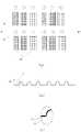
- spacer 12sub-pixel 13: cathode 14: cathode at a first region 15: pixel definition layer 16: cathode at a second region
- any technical or scientific term used hereinshall have the common meaning understood by a person of ordinary skills.
- Such words as “first” and “second” used in the specification and claimsare merely used to differentiate different components rather than to represent any order, number or importance.
- such words as “one” or “one of'are merely used to represent the existence of at least one member, rather than to limit the number thereof.
- Such words as “connect” or “connected to”may include electrical connection, direct or indirect, rather than to be limited to physical or mechanical connection.
- Such words as “on”, “under”, “left” and “right”are merely used to represent relative position relationship, and when an absolute position of the object is changed, the relative position relationship will be changed too.
- the present disclosureprovides in some embodiments an OLED array substrate and a method for manufacturing the same, an OLED packaging structure and a display device, so as to make the lap joint of the cathode firm and reduce the power consumption of the OLED array substrate without reducing the light transmittance of the OLED array substrate.
- Fig.1is a plan view of an OLED array substrate.
- Fig.2is a sectional view of the OLED array substrate shown in Fig.1 along Line B-B'.
- Fig.3is an enlarged view of the portion A of the OLED array substrate shown in Fig.2 .
- Thin film transistors, pixel definition layers, anodes, organic functional layers and cathodesare formed on the OLED array substrate.
- the pixel definition layerdefines a plurality of sub-pixels 12.
- a top light-emitting OLED apparatusis generally provided with relative thin cathodes 13 so as to achieve a relative high light transmittance.
- the OLED array substrateneed to be packaged with a packaging substrate, so spacers 11 are needed to be arranged between the OLED array substrate and the packaging substrate to support them and then form a cell gap therebetween.
- Each spacer 11includes a planarization layer resin and a pixel definition layer resin formed in advance of the cathodes.
- the cathodes 13cover the spacers 11.
- Each spacer 11is of a certain thickness, so the surface of the OLED array substrate is uneven at the regions where the spacers 11 are located and nearby. As shown in Fig.3 , a lap joint of a relative thin cathode may be poor at each spacer 11, and then a resistance of each cathode 13 may be increased and a power consumption of the OLED array substrate may be increased as a result. Nevertheless, the light transmittance of the OLED array substrate may be decreased and then the display effect may be influenced adversely if the cathode is thick.
- an OLED array substrateincluding thin film transistors, anodes, cathodes and organic light-emitting layers arranged between the anodes and the cathodes.
- the OLED array substratefurther includes first spacers configured to support the OLED array substrate and a packaging substrate so as to form a cell gap therebetween.
- Each cathodeincludes a first region which covers the corresponding first spacer and a second region beyond the first regions, and a thickness of the cathode at the first region is larger than a thickness of the cathode at the second region.
- the surface of the OLED array substrateis not even at the regions where the spacers are located.
- the cathodes at the regions where the spacers are locatedare thickened without changing the thicknesses of the cathodes at the other regions, so as to make the lap joint of the cathode at an uneven portion of the surface of the OLED apparatus firm and reduce the cathode resistance without reducing the light transmittance of the cathodes at the light-emitting regions, thereby to reduce a power consumption of the OLED array substrate.
- Fig.4is a plan view of an OLED array substrate according to some embodiments of the present disclosure.
- Fig.5is a sectional view of the OLED array substrate shown in Fig.4 along Line B-B'.
- Fig.6is an enlarged view of the portion C of the OLED array substrate shown in Fig.5 .
- each cathode of the OLED array substrateincludes a first region which covers the corresponding first spacer 11 and a second region beyond the first regions, and a thickness of the cathode 14 at the first region is larger than a thickness of the cathode 16 at the second region.
- the cathodes 14 at the first regionsare of an identical thickness
- the cathodes16 at the second regionsare of an identical thickness
- the cathode 14 at each first regionis of a thickness larger than the cathode 16 at each second region by 1 to 20 nanometers.
- only a part of each cathodesare thickened, so as to make the lap joint of the cathode at an uneven portion of the surface of the OLED apparatus firm and reduce the cathode resistance without influencing adversely the light transmittance of the cathodes at the light-emitting regions, thereby to reduce a power consumption of the OLED array substrate.
- An OLED packaging structureis further provided in some embodiments of the present disclosure, including the OLED array substrate hereinabove and a packaging substrate.
- the OLED packaging structurefurther includes second spacers configured to support the OLED array substrate and the packaging substrate so as to form a cell gap therebetween.
- the second spacersare arranged in the sealant.
- Each spaceris of a certain thickness, so the surface of the OLED array substrate is not even at the regions where the spacers are located.
- the cathodes at the regions where the spacers are locatedare thickened without changing the thicknesses of the cathodes at the other regions, so as to make the lap joint of the cathode at an uneven portion of the surface of the OLED apparatus firm and reduce the cathode resistance without reducing the light transmittance of the cathodes at the light-emitting regions, thereby to reduce a power consumption of the OLED array substrate.
- a display deviceis further provided in some embodiments of the present disclosure, including the OLED packaging structure hereinabove.
- the display devicemay be any product or component with a display function such as cell phones, tablet PCs, televisions, displayers, laptop computers, digital frames and navigators.
- Fig.1is a plan view of an OLED array substrate.
- Fig.2is a sectional view of the OLED array substrate shown in Fig.1 along Line B-B'.
- Fig.3is an enlarged view of the portion A of the OLED array substrate shown in Fig.2 .
- Thin film transistors, pixel definition layers, anodes, organic functional layers and cathodesare formed on the OLED array substrate.
- the pixel definition layerdefines a plurality of sub-pixels 12.
- a top light-emitting OLED apparatusis generally provided with relative thin cathodes 13 so as to achieve a relative high light transmittance.
- the OLED array substrateneed to be packaged with a packaging substrate, so spacers 11 are arranged between the OLED array substrate and the packaging substrate to support them and then form a cell gap therebetween.
- Each spacer 11includes a planarization layer resin and a pixel definition layer resin formed in advance of the cathodes.
- the cathodes 13cover the spacers 11.
- Each spacer 11is of a certain thickness, so the surface of the OLED array substrate is uneven at the regions where the spacers 11 are located. As shown in Fig.3 , a lap joint of a relative thin cathode may be poor at each spacer 11, and then a resistance of each cathode 13 may be increased and a power consumption of the OLED array substrate may be increased as a result. Nevertheless, the light transmittance of the OLED array substrate may be decreased and then the display effect may be influenced adversely if the cathode is thick.
- the OLED array substrateincludes thin film transistors, anodes, cathodes and organic light-emitting layers arranged between the anodes and the cathodes.
- the OLED array substratefurther includes spacers configured to support the OLED array substrate and a packaging substrate so as to form a cell gap therebetween.
- the methodincludes forming the cathodes on a substrate provided with the spacers, the thin film transistors, the anodes and the organic light-emitting layers, wherein each cathode includes a first region which covers the corresponding spacer and a second region beyond the first region, a thickness of the cathode at each first region is larger than a thickness of the cathode at each second region.
- Fig.4is a plan view of an OLED array substrate according to some embodiments of the present disclosure.
- Fig.5is a sectional view of the OLED array substrate shown in Fig.4 along Line B-B'.
- Fig.6is an enlarged view of the portion C of the OLED array substrate shown in Fig.5 .
- each cathode of the OLED array substrateincludes a first region which covers the corresponding first spacer 11 and a second region beyond the first regions, and a thickness of the cathode 14 at the first region is larger than a thickness of the cathode 16 at the second region.
- the cathodes 14 at the first regionsare of an identical thickness
- the cathodes 16 at the second regionsare of an identical thickness
- the cathode 14 at each first regionis of a thickness larger than the cathode 16 at each second region by 1 to 20 nanometers.
- the step of forming the cathodesincludes forming a first cathode pattern corresponding to the first regions and the second regions on the substrate provided with the spacers, the thin film transistors, the anodes and the organic light-emitting layers; and forming, on the first cathode pattern, a second cathode pattern corresponding to the first regions, wherein the cathodes are formed by the first and the second cathode patterns.
- the first regionsfurther include a second cathode pattern, so the cathode at each first region is of a thickness larger than the cathode at each second region.
- the second cathode patternmay be formed on substrate arranged with the first cathode pattern by evaporation.
- the step of forming, on the first cathode pattern, the second cathode pattern corresponding to the first regionsincludes attaching the substrate provided with the first cathode pattern and an evaporation mask closely, the evaporation mask including openings corresponding to the first regions; and forming the second cathode pattern on the substrate through evaporation using a cathode evaporating source arranged opposite to the evaporation mask.
- each cathodesis thickened, so as to make the lap joint of the cathode at an uneven portion of the surface of the OLED apparatus firm and reduce the cathode resistance without influencing adversely the light transmittance of the cathodes at the light-emitting regions, thereby to reduce a power consumption of the OLED array substrate.
Landscapes
- Physics & Mathematics (AREA)
- Optics & Photonics (AREA)
- Engineering & Computer Science (AREA)
- Microelectronics & Electronic Packaging (AREA)
- Manufacturing & Machinery (AREA)
- Electroluminescent Light Sources (AREA)
- Devices For Indicating Variable Information By Combining Individual Elements (AREA)
Description
- The present disclosure relates to the field of display technology, and in particular to an organic light emitting diode (OLED) array substrate and a method for manufacturing the same, an OLED packaging structure and a display device.
- OLED apparatus has the advantages such as all-solid-state structure, high brightness, full viewing angle, quick response, wide working temperature range, capable of achieving flexible display, and therefore has become a competitive and promising new generation of display technology. The organic light emitting material and the cathode material of the OLED apparatus are sensitive to moisture and oxygen, a service life of the OLED apparatus may be influenced adversely in a wet or highoxygen-content environment.
- In order to prevent moisture and oxygen from influencing adversely the OLED apparatus, the OLED apparatus is required to be packaged. In the process of packaging, the OLED array substrate is adhered to a packaging substrate by a sealant, thereby to form a sealed apparatus structure and block moisture and oxygen in the air. A spacer is arranged between the OLED array substrate and the packaging substrate, so to support them and form a cell gap therebetween.
- A top light-emitting OLED apparatus is generally provided with a relative thin cathode so as to achieve a relative high light transmittance. However, a surface of the OLED array substrate is not even, a lap joint of the thin cathode may be poor at an uneven portion of the surface of the OLED array substrate (e.g., where the spacers are located), therefore a cathode resistance may be increased and a power consumption of the OLED array substrate may be increased as a result. Nevertheless, the light transmittance of the OLED array substrate may be decreased and then the display effect may be influenced adversely if the cathode is thick.
CN 104064686 A discloses an organic light-emitting display device. The organic light-emitting display device includes a first substrate, a second substrate, a plurality of organic light-emitting elements and a conductive layer. The first substrate and the second substrate are arranged opposite each other. The organic light-emitting elements are arranged on the side of the first substrate facing the second substrate. Each organic light-emitting element includes an anode arranged on the first substrate, an organic light-emitting layer arranged on the anode and a cathode arranged on the organic light-emitting layer. The conductive layer is arranged on the side of the second substrate facing the first substrate and contacted with the cathodes.EP 2 182 564 A1 discloses an organic light emitting display device. The organic light emitting display device includes a plurality of light emitting elements on a first substrate, each of the plurality of light emitting elements including a first electrode and an organic light emitting layer, and a second electrode on the plurality of light emitting elements; a second substrate facing the first substrate with the plurality of light emitting elements therebetween; spacers on the second substrate corresponding to portions of the second electrode, the portions located on spaces between the plurality of light emitting elements; and an auxiliary electrode on the spacers and contacting the second electrode.CN 103943663 A discloses an OLED display device. The OLED display device includes an array substrate and a package substrate which are packaged together. The array substrate includes a first electrode layer, a second electrode layer and a light-emitting function layer located between the first electrode layer and the second electrode layer. The first electrode layer includes a plurality of pixel electrodes which are not contacted with one another. The second electrode layer comprises a plurality of second electrodes which are not contacted with one another, and each second electrode corresponds to at least one pixel electrode. The OLED display device further includes transmission leads, and each transmission lead corresponds to one of the second electrodes so as to input electric signals into the corresponding second electrode.CN 103022378 A discloses an organic light emitting diode (OLED) and a packaging method. The OLED device includes an array substrate and a packaging substrate. An OLED structure is manufactured on the surface of the array substrate. The edge of the array substrate and the edge of the packaging substrate are bonded and fixed through frame sealing glue. The OLED structure is located between the array substrate and the packaging substrate. A moisture-proof layer used for blocking water vapor and oxygen is manufactured on the surface of the OLED structure. A drying agent layer is located between the moisture-proof layer and the packaging substrate, wherein the drying agent layer includes drying agent particles which are used for absorbing water vapor and oxygen in the OLED device.US 2001/0043046 A1 provides a luminescent apparatus having a bright, high-quality image. A reflecting surface-including electrode, and an EL element formed of an organic EL layer and a transparent electrode are provided on an insulator. An auxiliary electrode formed of a transparent conductive film is connected to the transparent electrode via a conductor. This structure enables a resistance value of the transparent electrode to be substantially lowered, and a uniform voltage to be applied to the organic EL layer.US 2014/0062290 A1 provides an organic light emitting display apparatus which includes a substrate, a display portion on the substrate, the display portion including a plurality of emission regions, each including an organic light emitting diode (OLED), and a plurality of non-emission regions protruding from between the plurality of emission regions, an encapsulation substrate facing the substrate, a sealing material bonding the substrate and the encapsulation substrate and sealing the display portion, and a filling material on a surface of the encapsulation substrate facing the display portion, the filling material being spaced apart from the OLED and being formed of a cured polyimide (PI).- The present disclosure provides an OLED array substrate and a method for manufacturing the same, an OLED packaging structure and a display device, as defined in the accompanying claims, so as to make the lap joint of the cathode firm and reduce the power consumption of the OLED array substrate without reducing the light transmittance of the OLED array substrate. It should be noted that the invention is defined by the attached claims, and any examples and embodiments not covered by these claims are to be understood as aspects contributing to the understanding of the invention.
- The surface of the OLED array substrate is not even at the regions of the spacers. According to the embodiments of the present disclosure, the cathodes at the regions where the spacers are located are thickened without changing the thicknesses of the cathodes at the other regions, so as to make the lap joint of the cathode at an uneven portion of the surface of the OLED apparatus firm and reduce the cathode resistance without reducing the light transmittance of the cathodes at the light-emitting regions, thereby to reduce a power consumption of the OLED array substrate.
Fig.1 is a plan view of an OLED array substrate;Fig.2 is a sectional view of the OLED array substrate shown inFig.1 along line B-B';Fig.3 is an enlarged view of the portion A of the OLED array substrate shown inFig.2 ;Fig.4 is a plan view of an OLED array substrate according to some embodiments of the present disclosure;Fig.5 is a sectional view of the OLED array substrate shown inFig.4 along line B-B'; andFig.6 is an enlarged view of the portion C of the OLED array substrate shown inFig.5 .- 11: spacer 12: sub-pixel 13: cathode 14: cathode at a first region 15: pixel definition layer 16: cathode at a second region
- In order to make the objects, the technical solutions and the advantages of the present disclosure more apparent, the present disclosure will be described hereinafter in conjunction with the drawings and embodiments. Obviously, the following embodiments merely relate to a part of, rather than all of, the embodiments of the present disclosure, and based on these embodiments, a person skilled in the art may, without any creative effort, obtain the other embodiments, which also fall within the scope of the present disclosure.
- Unless otherwise defined, any technical or scientific term used herein shall have the common meaning understood by a person of ordinary skills. Such words as "first" and "second" used in the specification and claims are merely used to differentiate different components rather than to represent any order, number or importance. Similarly, such words as "one" or "one of' are merely used to represent the existence of at least one member, rather than to limit the number thereof. Such words as "connect" or "connected to" may include electrical connection, direct or indirect, rather than to be limited to physical or mechanical connection. Such words as "on", "under", "left" and "right" are merely used to represent relative position relationship, and when an absolute position of the object is changed, the relative position relationship will be changed too.
- The present disclosure provides in some embodiments an OLED array substrate and a method for manufacturing the same, an OLED packaging structure and a display device, so as to make the lap joint of the cathode firm and reduce the power consumption of the OLED array substrate without reducing the light transmittance of the OLED array substrate.
Fig.1 is a plan view of an OLED array substrate.Fig.2 is a sectional view of the OLED array substrate shown inFig.1 along Line B-B'.Fig.3 is an enlarged view of the portion A of the OLED array substrate shown inFig.2 .- Thin film transistors, pixel definition layers, anodes, organic functional layers and cathodes are formed on the OLED array substrate. The pixel definition layer defines a plurality of
sub-pixels 12. A top light-emitting OLED apparatus is generally provided with relativethin cathodes 13 so as to achieve a relative high light transmittance. However, the OLED array substrate need to be packaged with a packaging substrate, so spacers 11 are needed to be arranged between the OLED array substrate and the packaging substrate to support them and then form a cell gap therebetween. Eachspacer 11 includes a planarization layer resin and a pixel definition layer resin formed in advance of the cathodes. Thecathodes 13 cover thespacers 11. Eachspacer 11 is of a certain thickness, so the surface of the OLED array substrate is uneven at the regions where thespacers 11 are located and nearby. As shown inFig.3 , a lap joint of a relative thin cathode may be poor at eachspacer 11, and then a resistance of eachcathode 13 may be increased and a power consumption of the OLED array substrate may be increased as a result. Nevertheless, the light transmittance of the OLED array substrate may be decreased and then the display effect may be influenced adversely if the cathode is thick. - In view of this, an OLED array substrate is provided in some embodiments of the present disclosure, including thin film transistors, anodes, cathodes and organic light-emitting layers arranged between the anodes and the cathodes. The OLED array substrate further includes first spacers configured to support the OLED array substrate and a packaging substrate so as to form a cell gap therebetween. Each cathode includes a first region which covers the corresponding first spacer and a second region beyond the first regions, and a thickness of the cathode at the first region is larger than a thickness of the cathode at the second region.
- The surface of the OLED array substrate is not even at the regions where the spacers are located. According to the present disclosure, the cathodes at the regions where the spacers are located are thickened without changing the thicknesses of the cathodes at the other regions, so as to make the lap joint of the cathode at an uneven portion of the surface of the OLED apparatus firm and reduce the cathode resistance without reducing the light transmittance of the cathodes at the light-emitting regions, thereby to reduce a power consumption of the OLED array substrate.
Fig.4 is a plan view of an OLED array substrate according to some embodiments of the present disclosure.Fig.5 is a sectional view of the OLED array substrate shown inFig.4 along Line B-B'.Fig.6 is an enlarged view of the portion C of the OLED array substrate shown inFig.5 . As shown inFigs.5 and 6 , each cathode of the OLED array substrate includes a first region which covers the correspondingfirst spacer 11 and a second region beyond the first regions, and a thickness of thecathode 14 at the first region is larger than a thickness of thecathode 16 at the second region.- Furthermore, the
cathodes 14 at the first regions are of an identical thickness, and the cathodes16 at the second regions are of an identical thickness. To be specific, thecathode 14 at each first region is of a thickness larger than thecathode 16 at each second region by 1 to 20 nanometers. In some embodiments of the present disclosure, only a part of each cathodes are thickened, so as to make the lap joint of the cathode at an uneven portion of the surface of the OLED apparatus firm and reduce the cathode resistance without influencing adversely the light transmittance of the cathodes at the light-emitting regions, thereby to reduce a power consumption of the OLED array substrate. - An OLED packaging structure is further provided in some embodiments of the present disclosure, including the OLED array substrate hereinabove and a packaging substrate.
- An edge of the OLED array substrate is adhered to an edge of the packaging substrate by a sealant. The OLED packaging structure further includes second spacers configured to support the OLED array substrate and the packaging substrate so as to form a cell gap therebetween. The second spacers are arranged in the sealant.
- Each spacer is of a certain thickness, so the surface of the OLED array substrate is not even at the regions where the spacers are located. According to the embodiments of the present disclosure, the cathodes at the regions where the spacers are located are thickened without changing the thicknesses of the cathodes at the other regions, so as to make the lap joint of the cathode at an uneven portion of the surface of the OLED apparatus firm and reduce the cathode resistance without reducing the light transmittance of the cathodes at the light-emitting regions, thereby to reduce a power consumption of the OLED array substrate.
- A display device is further provided in some embodiments of the present disclosure, including the OLED packaging structure hereinabove. The display device may be any product or component with a display function such as cell phones, tablet PCs, televisions, displayers, laptop computers, digital frames and navigators.
Fig.1 is a plan view of an OLED array substrate.Fig.2 is a sectional view of the OLED array substrate shown inFig.1 along Line B-B'.Fig.3 is an enlarged view of the portion A of the OLED array substrate shown inFig.2 .- Thin film transistors, pixel definition layers, anodes, organic functional layers and cathodes are formed on the OLED array substrate. The pixel definition layer defines a plurality of
sub-pixels 12. A top light-emitting OLED apparatus is generally provided with relativethin cathodes 13 so as to achieve a relative high light transmittance. However, the OLED array substrate need to be packaged with a packaging substrate, so spacers 11 are arranged between the OLED array substrate and the packaging substrate to support them and then form a cell gap therebetween. Eachspacer 11 includes a planarization layer resin and a pixel definition layer resin formed in advance of the cathodes. Thecathodes 13 cover thespacers 11. Eachspacer 11 is of a certain thickness, so the surface of the OLED array substrate is uneven at the regions where thespacers 11 are located. As shown inFig.3 , a lap joint of a relative thin cathode may be poor at eachspacer 11, and then a resistance of eachcathode 13 may be increased and a power consumption of the OLED array substrate may be increased as a result. Nevertheless, the light transmittance of the OLED array substrate may be decreased and then the display effect may be influenced adversely if the cathode is thick. - In view of this, a method for manufacturing an OLED array substrate is further provided. The OLED array substrate includes thin film transistors, anodes, cathodes and organic light-emitting layers arranged between the anodes and the cathodes. The OLED array substrate further includes spacers configured to support the OLED array substrate and a packaging substrate so as to form a cell gap therebetween. The method includes forming the cathodes on a substrate provided with the spacers, the thin film transistors, the anodes and the organic light-emitting layers, wherein each cathode includes a first region which covers the corresponding spacer and a second region beyond the first region, a thickness of the cathode at each first region is larger than a thickness of the cathode at each second region.
Fig.4 is a plan view of an OLED array substrate according to some embodiments of the present disclosure.Fig.5 is a sectional view of the OLED array substrate shown inFig.4 along Line B-B'.Fig.6 is an enlarged view of the portion C of the OLED array substrate shown inFig.5 . As shown inFigs.5 and 6 , each cathode of the OLED array substrate includes a first region which covers the correspondingfirst spacer 11 and a second region beyond the first regions, and a thickness of thecathode 14 at the first region is larger than a thickness of thecathode 16 at the second region.- Furthermore, the
cathodes 14 at the first regions are of an identical thickness, and thecathodes 16 at the second regions are of an identical thickness. To be specific, thecathode 14 at each first region is of a thickness larger than thecathode 16 at each second region by 1 to 20 nanometers. - Furthermore, the step of forming the cathodes includes forming a first cathode pattern corresponding to the first regions and the second regions on the substrate provided with the spacers, the thin film transistors, the anodes and the organic light-emitting layers; and forming, on the first cathode pattern, a second cathode pattern corresponding to the first regions, wherein the cathodes are formed by the first and the second cathode patterns.
- As compared with the second regions, the first regions further include a second cathode pattern, so the cathode at each first region is of a thickness larger than the cathode at each second region.
- To be specific, the second cathode pattern may be formed on substrate arranged with the first cathode pattern by evaporation. The step of forming, on the first cathode pattern, the second cathode pattern corresponding to the first regions includes attaching the substrate provided with the first cathode pattern and an evaporation mask closely, the evaporation mask including openings corresponding to the first regions; and forming the second cathode pattern on the substrate through evaporation using a cathode evaporating source arranged opposite to the evaporation mask.
- In some embodiments of the present disclosure, only a part of each cathodes is thickened, so as to make the lap joint of the cathode at an uneven portion of the surface of the OLED apparatus firm and reduce the cathode resistance without influencing adversely the light transmittance of the cathodes at the light-emitting regions, thereby to reduce a power consumption of the OLED array substrate.
- The above are merely the preferred embodiments of the present disclosure.
Claims (8)
- An organic light emitting diode (OLED) array substrate, comprising:thin film transistors, anodes, cathodes (13) and organic light-emitting layers arranged between the anodes and the cathodes (13), wherein the OLED array substrate further comprises first spacers (11) configured to support the OLED array substrate and a packaging substrate so as to form a cell gap therebetween,each cathode (13) comprises a first region (14) which covers the corresponding first spacer (11) and a second region (16) beyond the first regions (14), and a thickness of the cathode (13) at the first region (14) is larger than a thickness of the cathode (13) at the second region (16),a projection of the first region (14) on the array substrate completely covers a projection of the corresponding first spacer (11) on the array substrate, and the cathodes (13) at the first regions (14) are of an identical thickness, the cathodes (13) at the second regions (16) are of an identical thickness,characterized in thatthe cathode (13) at each first region (14) is of a thickness larger than the cathode (13) at each second region (16) by 1 to 20 nanometers.
- An organic light emitting diode (OLED) packaging structure, comprising the OLED array substrate according to claim 1 and a packaging substrate.
- The OLED packaging structure according to claim 2, wherein an edge of the OLED array substrate is adhered to an edge of the packaging substrate by a sealant.
- The OLED packaging structure according to claim 3, further comprising:
second spacers configured to support the OLED array substrate and the packaging substrate so as to form a cell gap therebetween, the second spacers being arranged in the sealant. - A display device,characterized in that the display device comprises the OLED packaging structure according to any one of claims 2-4.
- A method for manufacturing an organic light emitting diode (OLED) array substrate, wherein the OLED array substrate comprises thin film transistors, anodes, cathodes (13) and organic light-emitting layers arranged between the anodes and the cathodes (13), the OLED array substrate further comprises spacers (11) configured to support the OLED array substrate and a packaging substrate so as to form a cell gap therebetween,
the method comprises:forming the cathodes (13) on a substrate provided with the spacers (11), the thin film transistors, the anodes and the organic light-emitting layers, wherein each cathode (13) comprises a first region (14) which covers the corresponding spacer (11) and a second region (16) beyond the first region (14), a thickness of the cathode (13) at each first region (14) is larger than a thickness of the cathode (13) at each second region (16),a projection of the first region (14) on the array substrate completely covers a projection of the corresponding spacer (11) on the array substrate, and the cathodes (13) at the first regions (14) are of an identical thickness,the cathodes (13) at the second regions (16) are of an identical thickness,characterized in thatthe cathode (13) at each first region (14) is of a thickness larger than the cathode (13) at each second region (16) by 1 to 20 nanometers. - The method according to claim 6, wherein the step of forming the cathodes (13) comprises:forming a first cathode pattern corresponding to the first regions (14) and the second regions (16) on the substrate provided with the spacers (11), the thin film transistors, the anodes and the organic light-emitting layers; andforming, on the first cathode pattern, a second cathode pattern corresponding to the first regions (14), wherein the cathodes (13) are formed by the first and the second cathode patterns.
- The method according to claim 7, wherein the step of forming, on the first cathode pattern, the second cathode pattern corresponding to the first regions (14) comprises:attaching the substrate provided with the first cathode pattern and an evaporation mask closely, the evaporation mask comprising openings corresponding to the first regions (14); andforming the second cathode pattern on the substrate through evaporation using a cathode evaporating source arranged opposite to the evaporation mask.
Applications Claiming Priority (2)
| Application Number | Priority Date | Filing Date | Title |
|---|---|---|---|
| CN201410832038.5ACN104465709B (en) | 2014-12-26 | 2014-12-26 | OLED array and preparation method thereof, encapsulating structure, display device |
| PCT/CN2015/094767WO2016101731A1 (en) | 2014-12-26 | 2015-11-17 | Oled array substrate, manufacturing method thereof, packaging structure and display device |
Publications (3)
| Publication Number | Publication Date |
|---|---|
| EP3240033A1 EP3240033A1 (en) | 2017-11-01 |
| EP3240033A4 EP3240033A4 (en) | 2018-08-15 |
| EP3240033B1true EP3240033B1 (en) | 2022-08-24 |
Family
ID=52911485
Family Applications (1)
| Application Number | Title | Priority Date | Filing Date |
|---|---|---|---|
| EP15860030.4ANot-in-forceEP3240033B1 (en) | 2014-12-26 | 2015-11-17 | Oled array substrate, manufacturing method thereof, packaging structure and display device |
Country Status (4)
| Country | Link |
|---|---|
| US (1) | US10205116B2 (en) |
| EP (1) | EP3240033B1 (en) |
| CN (1) | CN104465709B (en) |
| WO (1) | WO2016101731A1 (en) |
Families Citing this family (9)
| Publication number | Priority date | Publication date | Assignee | Title |
|---|---|---|---|---|
| CN104465709B (en)* | 2014-12-26 | 2017-06-23 | 京东方科技集团股份有限公司 | OLED array and preparation method thereof, encapsulating structure, display device |
| CN106328825B (en)* | 2016-10-31 | 2019-01-15 | 武汉华星光电技术有限公司 | OLED display |
| CN107180843B (en) | 2017-05-17 | 2020-02-18 | 京东方科技集团股份有限公司 | A package panel, device package structure and preparation method thereof |
| CN108538905B (en)* | 2018-05-31 | 2021-03-16 | 武汉华星光电半导体显示技术有限公司 | OLED light-emitting device and OLED display device |
| CN111524460B (en)* | 2020-04-26 | 2021-10-01 | 武汉华星光电半导体显示技术有限公司 | Display panel, mask plate and manufacturing method of display panel |
| CN111394692B (en)* | 2020-05-09 | 2022-05-13 | 京东方科技集团股份有限公司 | mask |
| CN111785852B (en)* | 2020-07-24 | 2023-09-22 | 京东方科技集团股份有限公司 | A display substrate, its manufacturing method, display panel and display device |
| CN112259698B (en)* | 2020-10-21 | 2022-08-09 | 京东方科技集团股份有限公司 | OLED film packaging method, packaging layer and OLED device |
| CN114335403B (en)* | 2021-12-15 | 2023-06-30 | 深圳市华星光电半导体显示技术有限公司 | Display panel, manufacturing method of display panel and machine for manufacturing display panel |
Citations (2)
| Publication number | Priority date | Publication date | Assignee | Title |
|---|---|---|---|---|
| US20010043046A1 (en)* | 2000-05-08 | 2001-11-22 | Takeshi Fukunaga | Luminescent apparatus and method of manufacturing the same |
| US20140062290A1 (en)* | 2012-09-04 | 2014-03-06 | Hoon Kim | Organic light emitting display apparatus and method of manufacturing the same |
Family Cites Families (10)
| Publication number | Priority date | Publication date | Assignee | Title |
|---|---|---|---|---|
| KR100822204B1 (en)* | 2006-06-07 | 2008-04-17 | 삼성에스디아이 주식회사 | Organic light emitting display device |
| KR100963075B1 (en)* | 2008-10-29 | 2010-06-14 | 삼성모바일디스플레이주식회사 | Organic light emitting display device |
| JP5625448B2 (en)* | 2010-03-31 | 2014-11-19 | 凸版印刷株式会社 | Method for manufacturing organic EL element and organic EL image display device |
| JP2012014868A (en)* | 2010-06-29 | 2012-01-19 | Sony Corp | Display device |
| KR101995700B1 (en)* | 2011-06-24 | 2019-07-03 | 가부시키가이샤 한도오따이 에네루기 켄큐쇼 | Light-emitting panel, light-emitting device using the light-emitting panel, and method for manufacturing the light-emitting panel |
| CN103022378B (en)* | 2012-12-17 | 2015-09-09 | 京东方科技集团股份有限公司 | A kind of OLED and method for packing, display unit |
| CN103943663A (en)* | 2014-04-25 | 2014-07-23 | 青岛海信电器股份有限公司 | OLED display device |
| CN104064686B (en)* | 2014-06-16 | 2017-01-18 | 上海天马有机发光显示技术有限公司 | Organic light-emitting display device |
| CN104465709B (en) | 2014-12-26 | 2017-06-23 | 京东方科技集团股份有限公司 | OLED array and preparation method thereof, encapsulating structure, display device |
| CN204257656U (en)* | 2014-12-26 | 2015-04-08 | 京东方科技集团股份有限公司 | OLED array, encapsulating structure and display unit |
- 2014
- 2014-12-26CNCN201410832038.5Apatent/CN104465709B/enactiveActive
- 2015
- 2015-11-17WOPCT/CN2015/094767patent/WO2016101731A1/enactiveApplication Filing
- 2015-11-17EPEP15860030.4Apatent/EP3240033B1/ennot_activeNot-in-force
- 2015-11-17USUS15/039,639patent/US10205116B2/enactiveActive
Patent Citations (2)
| Publication number | Priority date | Publication date | Assignee | Title |
|---|---|---|---|---|
| US20010043046A1 (en)* | 2000-05-08 | 2001-11-22 | Takeshi Fukunaga | Luminescent apparatus and method of manufacturing the same |
| US20140062290A1 (en)* | 2012-09-04 | 2014-03-06 | Hoon Kim | Organic light emitting display apparatus and method of manufacturing the same |
Also Published As
| Publication number | Publication date |
|---|---|
| CN104465709A (en) | 2015-03-25 |
| EP3240033A4 (en) | 2018-08-15 |
| WO2016101731A1 (en) | 2016-06-30 |
| US20170170423A1 (en) | 2017-06-15 |
| CN104465709B (en) | 2017-06-23 |
| US10205116B2 (en) | 2019-02-12 |
| EP3240033A1 (en) | 2017-11-01 |
Similar Documents
| Publication | Publication Date | Title |
|---|---|---|
| EP3240033B1 (en) | Oled array substrate, manufacturing method thereof, packaging structure and display device | |
| KR102424974B1 (en) | display device | |
| US10886481B2 (en) | Display substrate with angle-adjusting portion, manufacturing method thereof, and display device | |
| US9502683B2 (en) | Sealing portion structure for display device | |
| US8957410B2 (en) | Organic light-emitting diode package structure and method for forming the same | |
| US20210359259A1 (en) | Display panel and display device | |
| US11165038B2 (en) | Display module and electronic device with auxiliary electrode layer on cathode layer | |
| CN108987608B (en) | OLED display panel, method for manufacturing the same, and display device | |
| US9698372B2 (en) | OLED touch control display device and manufacture method thereof | |
| JP5908955B2 (en) | Touch screen and manufacturing method thereof | |
| US10289229B2 (en) | Touch panel with reduced electromagnetic interference | |
| US20150379921A1 (en) | Organic Light-Emitting Diode Display With Supplemental Power Supply Distribution Paths | |
| WO2016015421A1 (en) | Array substrate, organic light-emitting diode display panel and display apparatus | |
| KR20160032798A (en) | display device | |
| CN104576697A (en) | Double-sided OLED (organic light emitting diode) display device and manufacture method thereof | |
| US11296181B2 (en) | Display panel packaging method | |
| US20130187135A1 (en) | Light emitting device | |
| US11289675B2 (en) | Display panel with support structure and method of manufacturing the same | |
| US10220607B2 (en) | Screen mask assembly | |
| CN108962963A (en) | Display panel and its manufacturing method, display device | |
| KR20150000571A (en) | Organic light emitting diode display device | |
| EP3276659B1 (en) | Display device including white light-emitting layer | |
| JP2015158672A (en) | Active matrix organic light-emitting diode panel and packaging method thereof | |
| US9337440B2 (en) | Organic luminescent display device | |
| CN204257656U (en) | OLED array, encapsulating structure and display unit |
Legal Events
| Date | Code | Title | Description |
|---|---|---|---|
| STAA | Information on the status of an ep patent application or granted ep patent | Free format text:STATUS: THE INTERNATIONAL PUBLICATION HAS BEEN MADE | |
| PUAI | Public reference made under article 153(3) epc to a published international application that has entered the european phase | Free format text:ORIGINAL CODE: 0009012 | |
| STAA | Information on the status of an ep patent application or granted ep patent | Free format text:STATUS: REQUEST FOR EXAMINATION WAS MADE | |
| 17P | Request for examination filed | Effective date:20160525 | |
| AK | Designated contracting states | Kind code of ref document:A1 Designated state(s):AL AT BE BG CH CY CZ DE DK EE ES FI FR GB GR HR HU IE IS IT LI LT LU LV MC MK MT NL NO PL PT RO RS SE SI SK SM TR | |
| AX | Request for extension of the european patent | Extension state:BA ME | |
| DAV | Request for validation of the european patent (deleted) | ||
| DAX | Request for extension of the european patent (deleted) | ||
| A4 | Supplementary search report drawn up and despatched | Effective date:20180717 | |
| RIC1 | Information provided on ipc code assigned before grant | Ipc:H01L 51/52 20060101ALI20180711BHEP Ipc:H01L 27/32 20060101AFI20180711BHEP | |
| STAA | Information on the status of an ep patent application or granted ep patent | Free format text:STATUS: EXAMINATION IS IN PROGRESS | |
| 17Q | First examination report despatched | Effective date:20200713 | |
| GRAP | Despatch of communication of intention to grant a patent | Free format text:ORIGINAL CODE: EPIDOSNIGR1 | |
| STAA | Information on the status of an ep patent application or granted ep patent | Free format text:STATUS: GRANT OF PATENT IS INTENDED | |
| INTG | Intention to grant announced | Effective date:20220504 | |
| GRAS | Grant fee paid | Free format text:ORIGINAL CODE: EPIDOSNIGR3 | |
| GRAA | (expected) grant | Free format text:ORIGINAL CODE: 0009210 | |
| STAA | Information on the status of an ep patent application or granted ep patent | Free format text:STATUS: THE PATENT HAS BEEN GRANTED | |
| AK | Designated contracting states | Kind code of ref document:B1 Designated state(s):AL AT BE BG CH CY CZ DE DK EE ES FI FR GB GR HR HU IE IS IT LI LT LU LV MC MK MT NL NO PL PT RO RS SE SI SK SM TR | |
| REG | Reference to a national code | Ref country code:CH Ref legal event code:EP | |
| REG | Reference to a national code | Ref country code:IE Ref legal event code:FG4D | |
| REG | Reference to a national code | Ref country code:AT Ref legal event code:REF Ref document number:1514250 Country of ref document:AT Kind code of ref document:T Effective date:20220915 Ref country code:DE Ref legal event code:R096 Ref document number:602015080508 Country of ref document:DE | |
| REG | Reference to a national code | Ref country code:DE Ref legal event code:R079 Ref document number:602015080508 Country of ref document:DE Free format text:PREVIOUS MAIN CLASS: H01L0027320000 Ipc:H10K0059000000 | |
| REG | Reference to a national code | Ref country code:LT Ref legal event code:MG9D | |
| REG | Reference to a national code | Ref country code:NL Ref legal event code:MP Effective date:20220824 | |
| PG25 | Lapsed in a contracting state [announced via postgrant information from national office to epo] | Ref country code:SE Free format text:LAPSE BECAUSE OF FAILURE TO SUBMIT A TRANSLATION OF THE DESCRIPTION OR TO PAY THE FEE WITHIN THE PRESCRIBED TIME-LIMIT Effective date:20220824 Ref country code:RS Free format text:LAPSE BECAUSE OF FAILURE TO SUBMIT A TRANSLATION OF THE DESCRIPTION OR TO PAY THE FEE WITHIN THE PRESCRIBED TIME-LIMIT Effective date:20220824 Ref country code:PT Free format text:LAPSE BECAUSE OF FAILURE TO SUBMIT A TRANSLATION OF THE DESCRIPTION OR TO PAY THE FEE WITHIN THE PRESCRIBED TIME-LIMIT Effective date:20221226 Ref country code:NO Free format text:LAPSE BECAUSE OF FAILURE TO SUBMIT A TRANSLATION OF THE DESCRIPTION OR TO PAY THE FEE WITHIN THE PRESCRIBED TIME-LIMIT Effective date:20221124 Ref country code:NL Free format text:LAPSE BECAUSE OF FAILURE TO SUBMIT A TRANSLATION OF THE DESCRIPTION OR TO PAY THE FEE WITHIN THE PRESCRIBED TIME-LIMIT Effective date:20220824 Ref country code:LV Free format text:LAPSE BECAUSE OF FAILURE TO SUBMIT A TRANSLATION OF THE DESCRIPTION OR TO PAY THE FEE WITHIN THE PRESCRIBED TIME-LIMIT Effective date:20220824 Ref country code:LT Free format text:LAPSE BECAUSE OF FAILURE TO SUBMIT A TRANSLATION OF THE DESCRIPTION OR TO PAY THE FEE WITHIN THE PRESCRIBED TIME-LIMIT Effective date:20220824 Ref country code:FI Free format text:LAPSE BECAUSE OF FAILURE TO SUBMIT A TRANSLATION OF THE DESCRIPTION OR TO PAY THE FEE WITHIN THE PRESCRIBED TIME-LIMIT Effective date:20220824 Ref country code:ES Free format text:LAPSE BECAUSE OF FAILURE TO SUBMIT A TRANSLATION OF THE DESCRIPTION OR TO PAY THE FEE WITHIN THE PRESCRIBED TIME-LIMIT Effective date:20220824 | |
| REG | Reference to a national code | Ref country code:AT Ref legal event code:MK05 Ref document number:1514250 Country of ref document:AT Kind code of ref document:T Effective date:20220824 | |
| PG25 | Lapsed in a contracting state [announced via postgrant information from national office to epo] | Ref country code:PL Free format text:LAPSE BECAUSE OF FAILURE TO SUBMIT A TRANSLATION OF THE DESCRIPTION OR TO PAY THE FEE WITHIN THE PRESCRIBED TIME-LIMIT Effective date:20220824 Ref country code:IS Free format text:LAPSE BECAUSE OF FAILURE TO SUBMIT A TRANSLATION OF THE DESCRIPTION OR TO PAY THE FEE WITHIN THE PRESCRIBED TIME-LIMIT Effective date:20221224 Ref country code:HR Free format text:LAPSE BECAUSE OF FAILURE TO SUBMIT A TRANSLATION OF THE DESCRIPTION OR TO PAY THE FEE WITHIN THE PRESCRIBED TIME-LIMIT Effective date:20220824 Ref country code:GR Free format text:LAPSE BECAUSE OF FAILURE TO SUBMIT A TRANSLATION OF THE DESCRIPTION OR TO PAY THE FEE WITHIN THE PRESCRIBED TIME-LIMIT Effective date:20221125 | |
| PG25 | Lapsed in a contracting state [announced via postgrant information from national office to epo] | Ref country code:SM Free format text:LAPSE BECAUSE OF FAILURE TO SUBMIT A TRANSLATION OF THE DESCRIPTION OR TO PAY THE FEE WITHIN THE PRESCRIBED TIME-LIMIT Effective date:20220824 Ref country code:RO Free format text:LAPSE BECAUSE OF FAILURE TO SUBMIT A TRANSLATION OF THE DESCRIPTION OR TO PAY THE FEE WITHIN THE PRESCRIBED TIME-LIMIT Effective date:20220824 Ref country code:DK Free format text:LAPSE BECAUSE OF FAILURE TO SUBMIT A TRANSLATION OF THE DESCRIPTION OR TO PAY THE FEE WITHIN THE PRESCRIBED TIME-LIMIT Effective date:20220824 Ref country code:CZ Free format text:LAPSE BECAUSE OF FAILURE TO SUBMIT A TRANSLATION OF THE DESCRIPTION OR TO PAY THE FEE WITHIN THE PRESCRIBED TIME-LIMIT Effective date:20220824 Ref country code:AT Free format text:LAPSE BECAUSE OF FAILURE TO SUBMIT A TRANSLATION OF THE DESCRIPTION OR TO PAY THE FEE WITHIN THE PRESCRIBED TIME-LIMIT Effective date:20220824 | |
| REG | Reference to a national code | Ref country code:DE Ref legal event code:R097 Ref document number:602015080508 Country of ref document:DE | |
| PG25 | Lapsed in a contracting state [announced via postgrant information from national office to epo] | Ref country code:SK Free format text:LAPSE BECAUSE OF FAILURE TO SUBMIT A TRANSLATION OF THE DESCRIPTION OR TO PAY THE FEE WITHIN THE PRESCRIBED TIME-LIMIT Effective date:20220824 Ref country code:EE Free format text:LAPSE BECAUSE OF FAILURE TO SUBMIT A TRANSLATION OF THE DESCRIPTION OR TO PAY THE FEE WITHIN THE PRESCRIBED TIME-LIMIT Effective date:20220824 | |
| PG25 | Lapsed in a contracting state [announced via postgrant information from national office to epo] | Ref country code:MC Free format text:LAPSE BECAUSE OF FAILURE TO SUBMIT A TRANSLATION OF THE DESCRIPTION OR TO PAY THE FEE WITHIN THE PRESCRIBED TIME-LIMIT Effective date:20220824 Ref country code:AL Free format text:LAPSE BECAUSE OF FAILURE TO SUBMIT A TRANSLATION OF THE DESCRIPTION OR TO PAY THE FEE WITHIN THE PRESCRIBED TIME-LIMIT Effective date:20220824 | |
| PLBE | No opposition filed within time limit | Free format text:ORIGINAL CODE: 0009261 | |
| REG | Reference to a national code | Ref country code:CH Ref legal event code:PL | |
| STAA | Information on the status of an ep patent application or granted ep patent | Free format text:STATUS: NO OPPOSITION FILED WITHIN TIME LIMIT | |
| GBPC | Gb: european patent ceased through non-payment of renewal fee | Effective date:20221124 | |
| REG | Reference to a national code | Ref country code:BE Ref legal event code:MM Effective date:20221130 | |
| PG25 | Lapsed in a contracting state [announced via postgrant information from national office to epo] | Ref country code:LI Free format text:LAPSE BECAUSE OF NON-PAYMENT OF DUE FEES Effective date:20221130 Ref country code:CH Free format text:LAPSE BECAUSE OF NON-PAYMENT OF DUE FEES Effective date:20221130 | |
| 26N | No opposition filed | Effective date:20230525 | |
| PG25 | Lapsed in a contracting state [announced via postgrant information from national office to epo] | Ref country code:SI Free format text:LAPSE BECAUSE OF FAILURE TO SUBMIT A TRANSLATION OF THE DESCRIPTION OR TO PAY THE FEE WITHIN THE PRESCRIBED TIME-LIMIT Effective date:20220824 Ref country code:LU Free format text:LAPSE BECAUSE OF NON-PAYMENT OF DUE FEES Effective date:20221117 | |
| PG25 | Lapsed in a contracting state [announced via postgrant information from national office to epo] | Ref country code:IE Free format text:LAPSE BECAUSE OF NON-PAYMENT OF DUE FEES Effective date:20221117 Ref country code:GB Free format text:LAPSE BECAUSE OF NON-PAYMENT OF DUE FEES Effective date:20221124 | |
| PG25 | Lapsed in a contracting state [announced via postgrant information from national office to epo] | Ref country code:FR Free format text:LAPSE BECAUSE OF NON-PAYMENT OF DUE FEES Effective date:20221130 Ref country code:BE Free format text:LAPSE BECAUSE OF NON-PAYMENT OF DUE FEES Effective date:20221130 | |
| PGFP | Annual fee paid to national office [announced via postgrant information from national office to epo] | Ref country code:DE Payment date:20231121 Year of fee payment:9 | |
| PG25 | Lapsed in a contracting state [announced via postgrant information from national office to epo] | Ref country code:HU Free format text:LAPSE BECAUSE OF FAILURE TO SUBMIT A TRANSLATION OF THE DESCRIPTION OR TO PAY THE FEE WITHIN THE PRESCRIBED TIME-LIMIT; INVALID AB INITIO Effective date:20151117 | |
| PG25 | Lapsed in a contracting state [announced via postgrant information from national office to epo] | Ref country code:CY Free format text:LAPSE BECAUSE OF FAILURE TO SUBMIT A TRANSLATION OF THE DESCRIPTION OR TO PAY THE FEE WITHIN THE PRESCRIBED TIME-LIMIT Effective date:20220824 | |
| PG25 | Lapsed in a contracting state [announced via postgrant information from national office to epo] | Ref country code:MK Free format text:LAPSE BECAUSE OF FAILURE TO SUBMIT A TRANSLATION OF THE DESCRIPTION OR TO PAY THE FEE WITHIN THE PRESCRIBED TIME-LIMIT Effective date:20220824 Ref country code:IT Free format text:LAPSE BECAUSE OF FAILURE TO SUBMIT A TRANSLATION OF THE DESCRIPTION OR TO PAY THE FEE WITHIN THE PRESCRIBED TIME-LIMIT Effective date:20220824 | |
| PG25 | Lapsed in a contracting state [announced via postgrant information from national office to epo] | Ref country code:TR Free format text:LAPSE BECAUSE OF FAILURE TO SUBMIT A TRANSLATION OF THE DESCRIPTION OR TO PAY THE FEE WITHIN THE PRESCRIBED TIME-LIMIT Effective date:20220824 | |
| PG25 | Lapsed in a contracting state [announced via postgrant information from national office to epo] | Ref country code:BG Free format text:LAPSE BECAUSE OF FAILURE TO SUBMIT A TRANSLATION OF THE DESCRIPTION OR TO PAY THE FEE WITHIN THE PRESCRIBED TIME-LIMIT Effective date:20220824 | |
| PG25 | Lapsed in a contracting state [announced via postgrant information from national office to epo] | Ref country code:MT Free format text:LAPSE BECAUSE OF FAILURE TO SUBMIT A TRANSLATION OF THE DESCRIPTION OR TO PAY THE FEE WITHIN THE PRESCRIBED TIME-LIMIT Effective date:20220824 | |
| REG | Reference to a national code | Ref country code:DE Ref legal event code:R119 Ref document number:602015080508 Country of ref document:DE |