EP3220481B1 - Waveguide slot array antenna - Google Patents
Waveguide slot array antennaDownload PDFInfo
- Publication number
- EP3220481B1 EP3220481B1EP15858572.9AEP15858572AEP3220481B1EP 3220481 B1EP3220481 B1EP 3220481B1EP 15858572 AEP15858572 AEP 15858572AEP 3220481 B1EP3220481 B1EP 3220481B1
- Authority
- EP
- European Patent Office
- Prior art keywords
- slot
- polarization
- radiation plate
- waveguide
- slots
- Prior art date
- Legal status (The legal status is an assumption and is not a legal conclusion. Google has not performed a legal analysis and makes no representation as to the accuracy of the status listed.)
- Active
Links
- 230000005855radiationEffects0.000claimsdescription159
- 230000010287polarizationEffects0.000claimsdescription89
- 230000005284excitationEffects0.000claimsdescription78
- 230000008878couplingEffects0.000claimsdescription24
- 238000010168coupling processMethods0.000claimsdescription24
- 238000005859coupling reactionMethods0.000claimsdescription24
- 238000013461designMethods0.000description11
- 238000005388cross polarizationMethods0.000description6
- 230000005684electric fieldEffects0.000description5
- 230000036544postureEffects0.000description4
- 238000003491arrayMethods0.000description3
- 239000000758substrateSubstances0.000description3
- 229910003460diamondInorganic materials0.000description2
- 239000010432diamondSubstances0.000description2
- NCGICGYLBXGBGN-UHFFFAOYSA-N3-morpholin-4-yl-1-oxa-3-azonia-2-azanidacyclopent-3-en-5-imine;hydrochlorideChemical compoundCl.[N-]1OC(=N)C=[N+]1N1CCOCC1NCGICGYLBXGBGN-UHFFFAOYSA-N0.000description1
- 230000005540biological transmissionEffects0.000description1
- 238000004891communicationMethods0.000description1
- 239000004020conductorSubstances0.000description1
- 230000006866deteriorationEffects0.000description1
- 230000009977dual effectEffects0.000description1
- 230000001747exhibiting effectEffects0.000description1
- 235000015250liver sausagesNutrition0.000description1
- 239000002184metalSubstances0.000description1
- 238000000034methodMethods0.000description1
- 238000012986modificationMethods0.000description1
- 230000004048modificationEffects0.000description1
- 238000012545processingMethods0.000description1
- 238000005476solderingMethods0.000description1
- 239000000126substanceSubstances0.000description1
- 238000003466weldingMethods0.000description1
Images


Classifications
- H—ELECTRICITY
- H01—ELECTRIC ELEMENTS
- H01Q—ANTENNAS, i.e. RADIO AERIALS
- H01Q21/00—Antenna arrays or systems
- H01Q21/06—Arrays of individually energised antenna units similarly polarised and spaced apart
- H01Q21/061—Two dimensional planar arrays
- H01Q21/064—Two dimensional planar arrays using horn or slot aerials
- H—ELECTRICITY
- H01—ELECTRIC ELEMENTS
- H01Q—ANTENNAS, i.e. RADIO AERIALS
- H01Q13/00—Waveguide horns or mouths; Slot antennas; Leaky-waveguide antennas; Equivalent structures causing radiation along the transmission path of a guided wave
- H01Q13/10—Resonant slot antennas
- H—ELECTRICITY
- H01—ELECTRIC ELEMENTS
- H01Q—ANTENNAS, i.e. RADIO AERIALS
- H01Q13/00—Waveguide horns or mouths; Slot antennas; Leaky-waveguide antennas; Equivalent structures causing radiation along the transmission path of a guided wave
- H01Q13/10—Resonant slot antennas
- H01Q13/106—Microstrip slot antennas
- H—ELECTRICITY
- H01—ELECTRIC ELEMENTS
- H01Q—ANTENNAS, i.e. RADIO AERIALS
- H01Q15/00—Devices for reflection, refraction, diffraction or polarisation of waves radiated from an antenna, e.g. quasi-optical devices
- H01Q15/24—Polarising devices; Polarisation filters
- H01Q15/242—Polarisation converters
- H01Q15/246—Polarisation converters rotating the plane of polarisation of a linear polarised wave
- H—ELECTRICITY
- H01—ELECTRIC ELEMENTS
- H01Q—ANTENNAS, i.e. RADIO AERIALS
- H01Q21/00—Antenna arrays or systems
- H—ELECTRICITY
- H01—ELECTRIC ELEMENTS
- H01Q—ANTENNAS, i.e. RADIO AERIALS
- H01Q21/00—Antenna arrays or systems
- H01Q21/0006—Particular feeding systems
- H01Q21/0037—Particular feeding systems linear waveguide fed arrays
- H01Q21/0043—Slotted waveguides
- H01Q21/005—Slotted waveguides arrays
- H—ELECTRICITY
- H01—ELECTRIC ELEMENTS
- H01Q—ANTENNAS, i.e. RADIO AERIALS
- H01Q21/00—Antenna arrays or systems
- H01Q21/06—Arrays of individually energised antenna units similarly polarised and spaced apart
- H—ELECTRICITY
- H01—ELECTRIC ELEMENTS
- H01Q—ANTENNAS, i.e. RADIO AERIALS
- H01Q21/00—Antenna arrays or systems
- H01Q21/06—Arrays of individually energised antenna units similarly polarised and spaced apart
- H01Q21/20—Arrays of individually energised antenna units similarly polarised and spaced apart the units being spaced along or adjacent to a curvilinear path
- H—ELECTRICITY
- H01—ELECTRIC ELEMENTS
- H01Q—ANTENNAS, i.e. RADIO AERIALS
- H01Q21/00—Antenna arrays or systems
- H01Q21/24—Combinations of antenna units polarised in different directions for transmitting or receiving circularly and elliptically polarised waves or waves linearly polarised in any direction
- H01Q21/245—Combinations of antenna units polarised in different directions for transmitting or receiving circularly and elliptically polarised waves or waves linearly polarised in any direction provided with means for varying the polarisation
Definitions
- the present disclosurerelates to a super high frequency transmitting and receiving antenna, and more particularly, to a waveguide slot array antenna.
- Super high frequency transmitting and receiving antennasinclude a parabolic-type antenna, a microstrip antenna, a waveguide slot array antenna, and so forth.
- a microstrip array antenna or a waveguide slot array antennais mainly used for miniaturization through thickness reduction.
- the microstrip array antennahas a microstrip patch array structure using a dielectric substrate, in which a loss of a transmitted or received signal is large depending on a loss coefficient of a dielectric based on characteristics of the dielectric substrate, and an ohmic loss of a conductor occurs, and the loss increases especially for a higher frequency, such that the use of the microstrip array antenna is avoided in a super high frequency band.
- the waveguide slot array antennahas a structure in which a hole in the form of a slot is formed in a general waveguide, without using the dielectric substrate.
- a waveguideis a hollow metal pipe and a sort of high pass filter in which a guided mode has a specific cutoff frequency and a dominant mode is determined by a size of the waveguide.
- the waveguidehas lower attenuation than a parallel two-wire line, a coaxial cable, etc., and thus is mostly used for high power in a microwave transmission line.
- the waveguidemay have various cross-sectional shapes, depending on which the waveguide is classified into a circular waveguide, a quadrangular waveguide, an oval waveguide, and so forth.
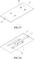
- FIG. 1Ais a perspective view in which each layer of a conventional waveguide slot array antenna having a stacked multi-layer structure is partially cut.
- the conventional waveguide slot array antennaincludes a feeding plate 11 in which an input feeding slot 112 is formed, a distribution plate 12 which is installed on the feeding plate 11 and in which a distributor and coupling slots 122 are formed, a main radiation plate 13 which is installed on the distribution plate 12 and in which a cavity structure and an excitation slot (or a radiation slot) 132 are formed, and an auxiliary radiation plate 14 which is installed on the main radiation plate 13 and in which a polarization slot 142 is formed to generate a polarized wave having a polarization plane inclined at 45 degrees(°).
- the input signalis distributed, for example, in an equal ratio, through the distribution plate 12, and each distributed signal is delivered to each cavity formed in the main radiation plate 13 through the coupling slots 122.
- the signal delivered to the cavity of the main radiation plate 13is distributed and radiated in an equal ratio through, for example, four excitation slots 132 formed for each cavity.
- the excitation slots 132are arranged to have a preset interval and preset arrangement therebetween according to an operating frequency.
- the polarization slots 142each of which one-to-one corresponds to each excitation slot 132 of the main radiation plate 13, is formed, and the signal delivered to the polarization slot 142 is rotated at 45 degrees when compared to radiation from the excitation slot 132 and is radiated to the space. That is, a wave polarized at 45 degrees in a vertical/horizontal direction is generated by the auxiliary radiation plate 14.
- the excitation slot 132has, for example, an approximately rectangular shape, and is formed in an erect position or posture in the vertical/horizontal direction
- the polarization slot 142has a rectangular shape similar to the approximately rectangular shape of the excitation slot 132, but when compared to the slot shape of the excitation slot 132, the rectangular shape of the polarization slot 142 is formed in a position or posture mechanically rotated at 45 degrees in the vertical/horizontal direction and thus may be globally similar to a diamond shape.
- Such a structuremay be regarded as a structure that forms one radiation slot by a combination of the excitation slot 132 and the polarization slot 142.
- the auxiliary radiation plate 14is used and the polarization slot 142 of the auxiliary radiation plate 14 may have a rectangular shape rotated at 45 degrees with respect to the excitation slot 132 to rotate a polarization plane of a signal radiated from the excitation slot 132 at 45 degrees.
- a side lobe componentis significantly suppressed by a total length of a vertical/horizontal plane.
- an arrangement interval between the polarization slots 142 on the vertical/horizontal planemay fail to satisfy a proper distance criterion required when a wavelength of an operating frequency is considered. That is, as indicated by a in FIG. 1A , a distance, especially between the polarization slots 142 arranged diagonally to each other may increase. Such a structure may cause a grating lobe.
- a distance between arraysexceeds one wavelength, a specific radiation angle is produced at which signals radiated from respective radiation slots are in phase.
- a lobe produced in this caseis called a grating lobe that is a sort of main lobe.
- the grating lobeis generated by a phase of an array element in the array antenna, and the phase is controlled by a distance between elements.
- FIG. 1Bshows a state in which a main lobe and a grating lobe are produced, for example, in positions P1 and P2 of two polarization slots located diagonally (having a distance of d therebetween) in FIG. 1A .
- a phase difference between two pathsis one wavelength ⁇
- the grating lobeis produced at an angle rotated by ⁇ from the main lobe.
- US 6,028,562 A1discloses an antenna comprising a planar array of waveguide slot radiators for communicating electromagnetic signals exhibiting simultaneous dual polarization states.
- the antennaconsists of parallel waveguides of rectangular or ridged cross section.
- the broadwalls of each parallel waveguidecontain a linear array of input slots for receiving or transmitting electromagnetic signals having a first polarization state from/to the parallel waveguide and for transmitting or receiving those signals into/from an array of cavity sections.
- the cavity sectionscomprise a short section of uniform waveguide with a length of much less than a wavelength in the propagation direction.
- the cavity sectionsfeed to output slots which are rotated relative to the input slots.
- KR 100 721 871 B1discloses a waveguide slot antenna for receiving random polarized satellite signal.
- the number of excitation slot arraysincreases to a power of 2 depending on a distribution plate and a cavity structure that distributes a signal on a main radiation plate, showing some limitations in the design of arrangement of excitation slots.
- the present disclosureis proposed to solve the foregoing problems, and provides a waveguide slot array antenna that generates a polarized wave while effectively suppressing a grating lobe.
- the present disclosurealso provides a waveguide slot array antenna that freely implements an overall antenna structure by improving the degree of freedom as to the design of a slot array.
- the first auxiliary radiation platemay include an array of first polarization slots formed to have a structure corresponding to the excitation slot array of the main radiation plate, and the first polarization slots may be structured to rotate a polarization plane of a signal radiated by a corresponding excitation slot.
- the second auxiliary radiation platemay include an array of a plurality of second polarization slots formed for each first polarization slot of the first auxiliary radiation plate, and a distribution structure for distributing a signal radiated for each first polarization slot of the first auxiliary radiation plate to the plurality of second polarization slots corresponding to the first polarization slot is formed in the second auxiliary radiation plate.
- the waveguide slot array antennamay further include a feeding plate which forms at least a part of a waveguide to be provided with an input signal and a distribution plate which includes a distribution waveguide structure coupled to the feeding plate to distribute the input signal to multiple coupling slots, in which the main radiation plate is installed on the distribution plate and includes multiple cavity structures for distributing a signal input through each coupling slot of the distribution plate in an equal ratio and exciting the distributed signal through the excitation slot array
- the waveguide slot array antennagenerates a polarized wave while effectively suppressing a grating lobe, thereby reducing an influence upon an adjacent device in an adjacent-fixed communication device.
- the waveguide slot array antenna according to the inventionmay improve the degree of freedom as to the design of slot arrangement, allowing free implementation of an overall antenna structure. Hence, the unnecessary increase of the antenna size may be prevented, and processing complexity may be reduced by maintaining a proper arrangement level, thereby reducing a loss of time cost.
- FIG. 2is a perspective view in which each layer of a waveguide slot array antenna having a stacked multi-layer structure is partially cut according to a first embodiment of the present disclosure.
- the waveguide slot array antenna according to the first embodiment of the present disclosuremay include a feeding plate 11 in which an input feeding slot 112 is formed, a distribution plate 12 which is installed on the feeding plate 11 and has a distributor and a coupling slot 122 formed therein, and a main radiation plate 13 which is installed on the distribution plate 12 and has a cavity structure and an excitation slot (or a radiation slot) 132 formed therein.
- the waveguide slot array antennamay further include a first auxiliary radiation plate which is installed on the main radiation plate 13 and has a first polarization slot 142 formed therein to generate a polarized wave having a polarization plane inclined at 45 degrees and a second auxiliary radiation plate 15 which is installed on the first auxiliary radiation plate 14 and has a second polarization slot 152 input through the feeding slot 112 of the feeding plate 11, the input signal is distributed in an equal ratio through the distribution plate 12, and each distributed signal is delivered to each cavity formed in the main radiation plate 13 through the coupling slots 122.
- the signal delivered to the cavity of the main radiation plate 13is distributed and radiated, for example, in an equal ratio through, for example, four excitation slots 132 formed for each cavity.
- the excitation slots 132are arranged to have a preset interval and preset arrangement therebetween according to an operating frequency.
- the first polarization slots 142are formed to one-to-one correspond to the respective excitation slots 132 of the main radiation plate 13.
- the first polarization slot 142is structured such that an approximately quadrangular (or rectangular) slot is formed in a posture mechanically rotated at 45 degrees with respect to the excitation slot 132. With this structure, for the signal delivered to the first polarization slot 142, a polarized wave signal is generated to have a polarization plane rotated at 45 degrees relative to the signal radiated from the excitation slot 132.
- a plurality of (e.g., two) second polarization slots 152are formed to correspond to each first polarization slot 142 of the first auxiliary radiation plate 14 and a distribution structure for distributing a signal to the plurality of corresponding second polarization slots 152 for each first polarization slot 142 is formed.
- Shapes (and postures) of the first polarization slot 142 and the plurality of second polarization slots 152may be the same as one another. With this structure, the polarized wave generated in the first polarization slot 142 is distributed and radiated through the second polarization slots 152.
- the first auxiliary radiation plate 14 and the second auxiliary radiation plate 15further include a structure for rotating a signal excited by the excitation slot 132 of the main radiation plate 13 such that the signal has a polarization plane inclined at 45 degrees and an extended slot array structure using an electric field plane or magnetic field plane signal distribution structure.
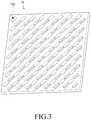
- FIG. 3is a perspective view of a top side (e.g., a front side along a signal radiation direction) of the second auxiliary radiation plate 15
- FIG. 4is a perspective view of a bottom side (e.g., a rear side along the signal radiation direction) of the second auxiliary radiation plate 15
- FIGs. 5 and 6are a perspective view and a side view showing a connection relationship between the second polarization slot 152 of the second auxiliary radiation plate 15 and the first polarization slot 142 of the first auxiliary radiation plate 14, respectively.
- an electric field of a signal delivered from the excitation slot 132 of the main radiation plate 13is fixed after rotated at 45 degrees in the first polarization slot 142 of the first auxiliary radiation plate 14, and then the signal is delivered toward the second polarization slot 152 of the second auxiliary radiation plate 15.
- the signal delivered to the second auxiliary radiation plate 15is distributed through the distribution structure formed under the second polarization slots 152, such that each distributed signal is provided to the plurality of second polarization slots 152.
- a distribution structuremay have a structure branched vertically or horizontally with respect to an electric field plane.
- the signal distributed and provided to the second polarization slot 152is radiated to the space and thus may be expressed in an overall antenna radiation pattern.
- an arrangement interval between the second polarization slots 152may be, for example, a half of an arrangement interval between the first polarization slots 142 of the first auxiliary radiation plate 14 according to a branched plane. That is, with this structure, an arrangement interval on a vertical/horizontal plane between the second polarization slots 152 formed in the second auxiliary radiation plate 15 may sufficiently satisfy a criterion of within one wavelength with respect to an operating frequency, thus sufficiently suppressing a grating lobe.
- FIG. 7is a perspective view showing a modified structure of the second polarization slot 152 of the second auxiliary radiation plate 15 and the first polarization slot 142 of the first auxiliary radiation plate 14 in FIG. 2 .
- a second polarization slot 152-1is formed in the second auxiliary radiation plate 15 without a distribution structure under the second polarization slot 152; instead, the distribution structure is formed above a first polarization slot 142-1 of the first auxiliary radiation plate 14. That is, in the modified structure shown in FIG. 7 , the second polarization slot 152-1 is formed in the second auxiliary radiation plate 15, and the first auxiliary radiation plate 14 has the first polarization slot 142-1 and the distribution structure formed above the first polarization slot 142-1.
- a shape of a waveguide path formed by the first polarization slot 142-1, the distribution structure, and the second polarization slot 152-1 to deliver an internal signal therethroughis substantially the same as a shape of a waveguide path formed by the structure shown in FIGs. 2 through 6 , and signal delivery characteristics are identical.
- FIG. 8is a perspective view of a side of the first auxiliary radiation plate 14 shown in FIG. 2
- FIG. 9is a perspective view of a top side (e.g., a front side along a signal radiation direction) of the radiation plate 13 shown in FIG. 2
- FIG. 10is a perspective view of a bottom side (e.g., a rear side in the signal radiation direction) of the radiation plate 13 shown in FIG. 2
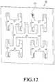
- FIGs. 11 and 12are perspective views of a top side and a side of the distribution plate 12 shown in FIG. 2
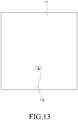
- FIG. 13is a plane view of the feeding plate 11 shown in FIG. 2 . Referring to FIGs.
- FIGs. 8 through 12are views according to an order in which plates are installed from a top side to a bottom side, but the following description will be made based on signal input and a waveguiding path.
- a waveguide(not shown) for guiding a signal input through an input connector (not shown), etc., is formed in a proper shape on a side with respect to a bottom surface of the feeding plate 11.
- the bottom surface of the feeding plate 11may be formed to be, for example, several millimeters to several tens of millimeters.
- the feeding slot 112is formed at a terminal of the waveguide of the feeding plate 11, and the feeding slot 112 may be a multistage slot to achieve matching according to a size of a distribution waveguide formed on the corresponding distribution plate 12.
- the rear surface of the feeding plate 11may be processed to have a hole or a tab corresponding to an engagement portion of a normalized waveguide flange.
- the distribution plate 12 connected with the feeding pate 11has a distribution waveguide structure for distributing a signal input through the feeding slot 112 of the feeding plate 11 to the multiple coupling slots 122.
- the number of branched final branches of the distribution waveguide structurecorresponds to distribution into a power of 2, and the branches are top-bottom and left-right symmetric.
- Such a distribution waveguide structuremay have an electric field or magnetic field distribution structure.
- the electric field or magnetic field distribution structuremay further include an iris structure and a septum structure, taking matching characteristics into account.
- the coupling slot 122is formed at a terminal of each branched final branch.
- the coupling slot 122is located one-sidedly by being offset from the center of a waveguide structure at the terminal of each final branch of the distribution waveguide structure, causing strong coupling.
- the main radiation plate 13 connected with the distribution plate 12distributes a signal input through each coupling slot 122 of the distribution plate 12 in an equal or unequal ratio, and has a cavity structure for exciting the distributed signal through each excitation slot 132.
- Each coupling slot 122 of the distribution plate 12is designed to be located in the center of a corresponding cavity of the main radiation plate 13.
- Each cavitymay be structured to have, for example, four excitation slots 132 formed therein, and to properly form a resonance condition of each of the four excitation slots 132, a septum having a predetermined length is formed on and perpendicular to each surface of the cavity.
- the feeding plate 11, the distribution plate 12, and the main radiation plate 13may be designed, and the first auxiliary radiation plate 14 and the second auxiliary radiation plate 15 are designed correspondingly thereto.
- the feeding plate 11, the distribution plate 12, the main radiation plate 13, the first auxiliary radiation plate 14, and the second auxiliary radiation plate 15are also aligned and mutually coupled to one another according to a designed structure.
- coupling between the platesmay use screw engagement using a screw, soldering, high-frequency welding, or the like.
- FIG. 14is a structural view of (a part of) an internal signal waveguide path of the waveguide slot array antenna according to the first embodiment of the present disclosure, in which a structure according to some embodiments of the present disclosure is shown in (b) of FIG. 14 , and an internal signal waveguide path (or a part thereof) of the conventional waveguide slot array antenna as shown in FIG. 1 is shown in (a) of FIG. 14 for comparison.
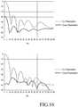
- FIG. 15is a graph showing grating lobe characteristics of the waveguide slot array antenna shown in FIG. 14
- FIG. 16is a graph showing cross polarization characteristics of the waveguide slot array antenna shown in FIG. 14 .
- a graph of characteristics according to the first embodiment of the present disclosureis shown in (b)
- a graph of characteristics of the conventional waveguide slot array antenna as shown in FIG. 1is shown in (a) for comparison.
- a waveguide slot array antenna according to the present disclosuremay be regarded as further including the second auxiliary radiation plate 15 when compared to a conventional waveguide slot array antenna, and although one layer (plate) is physically further stacked, an overall height of the antenna may be the same as that of the conventional antenna. That is, as shown in FIG. 14 , an overall height h1 of the conventional antenna and an overall height h2 of the antenna according to the present disclosure may be equal to each other. In such a design, as shown in FIG. 15 , grating lobe characteristics of the antenna according to the present disclosure are further improved in spite of primary and secondary side lobes having sizes equal to those of the conventional antenna.
- a height of a radiation slot at a final stagedominantly works as a determinant of cross polarization.
- a height h21 of a radiation slot (a second polarization slot) at a final stage of the antenna according to the present disclosureis designed to be smaller than a height h11 of a radiation slot (a first polarization slot) at a final stage of the conventional antenna.
- the present disclosuremay optimally design the height of the radiation slot at the final stage of the antenna.
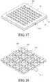
- FIG. 17is a perspective view of main portions of a waveguide slot array antenna for comparison with embodiments of the present disclosure
- FIG. 18is a structural view of an internal signal waveguide path of the waveguide slot array antenna shown in FIG. 17
- the waveguide slot array antenna shown in FIGs. 17 and 18may basically include a structure in which the feeding plate 21, the distribution plate 22, and the radiation plate 23 are sequentially stacked in that order, like the structure according to the first embodiment shown in FIG. 2 and other drawings.
- auxiliary radiation plate(s)may be further installed on the radiation plate 23 to generate a polarized wave, similarly with the structure shown in FIG. 2 and other drawings.
- a structure for providing an input signal through a feeding slot of a feeding plateis desclosed as an example, but in FIGs. 17 and 18 , a structure for providing an input signal through a feeding waveguide 212 having an open section for signal input formed in a side of the distribution plate 22 is shown as an example.
- the distribution plate 22forms the feeding waveguide 212 and a hollow region of a distribution waveguide structure for distributing a signal input through the feeding waveguide 212, and the feeding plate 21 may simply have the form of a flat plate.
- the signalis distributed in an equal ratio through the distribution plate 22 and the distributed signal is delivered to each cavity 220 formed in the radiation plate 23.
- the signal delivered to the cavity 220 of the radiation plate 23is distributed and radiated, for example, in an equal ratio through, for example, four excitation slots 232 formed for each cavity 220.
- the excitation slots 232are arranged to have a preset interval and preset arrangement therebetween according to an operating frequency.
- an input signalis distributed into a power of 2, for example, equally, in the distribution plate 22, and the signal distributed and then finally radiated through the excitation slot 232 in the radiation plate 23 is distributed into a power of 2, such that the excitation slots 232 are arranged in the form of a power of 2, such as 2 ⁇ 2, 4 ⁇ 4, or the like.
- a signal that is input through one coupling slot of the distribution plate 22 and delivered to one cavity of the radiation plate 23is radiated through four excitation slots 232 formed for each cavity.
- this structurehas an array of a total of 4 ⁇ 4, 8 ⁇ 8, 16 ⁇ 16, etc. excitation slots 232.
- a signal distribution structureuses an H-junction structure, thereby implementing a symmetric and efficient feeding network structure.
- H-junction structuredue to such a structure, there are a limitation in horizontal and vertical beam patterns, a difficulty in the flexible design of a gain, and an unnecessarily large volume.
- the H-junction structureis not easy to adopt and a separate additional layer may be needed for implementation of a desired structure array, increasing an overall thickness and thus limiting a low-profile design.
- an arrangement interval between excitation slotsmay be narrowed when compared to in other embodiments shown in FIG. 2 and other drawings, and thus, according to circumstances, when the first auxiliary radiation plate as shown in FIG. 2 is provided, a grating lobe may be suppressed without a need for the separate second auxiliary radiation plate on the first auxiliary radiation plate.
- FIG. 19is a perspective view of main portions of a waveguide slot array antenna according to a second embodiment of the present disclosure
- FIG. 20is a structural view of an internal signal waveguide path of the waveguide slot array antenna shown in FIG. 19 , showing an example of a basic structure in which excitation slots are arranged in a minimum array unit (e.g., 4 ⁇ 2).
- a minimum array unite.g. 4 ⁇ 2
- the waveguide slot array antenna according to the second embodiment of the present disclosurelike the structure shown in FIGs.
- 17 and 18may include a feeding plate 31, a distribution plate 32 which is installed stacked on the feeding plate 31 and has a feeding waveguide 312 and a waveguide structure for delivering a signal input through the feeding waveguide 312 to a radiation plate 33 through a coupling slot (not shown), and the radiation plate 33 which is installed stacked on the distribution plate 32 and has multiple first through eighth excitation slots 332 (332-1, 332-2, 332-3 332-4, 332-5, 332-6 , 332-7, and 332-8) formed therein and a cavity structure 330 which distributes the signal input through the coupling slot of the distribution plate 32 and excites the distributed signal through the excitation slots 332.
- auxiliary radiation plate(s)may be further installed on the radiation plate 33 to generate a polarized wave.
- the cavity structure 330 of the radiation plate 33is divided into four first through fourth regions a, b, c, and d for distributing the signal provided from the distribution plate 32, for example, equally, into four parts, and correspondingly, septums having a predetermined length are formed on and perpendicular to each surface of the cavity.
- septumshaving a predetermined length are formed on and perpendicular to each surface of the cavity.
- two excitation slotsare formed unlike in the structure shown in FIGs. 17 and 18 .
- the first and second excitation slots 332-1 and 332-2may be formed and designed such that the centers thereof are offset from an array reference axis (e.g., a vertical axis) in opposite directions to each other.
- an array reference axise.g., a vertical axis
- Such an array structure of the excitation slotsenables a strength of a signal provided to each excitation slot to be as strong as possible and to be equally distributed.
- the third and fourth excitation slots 332-3 and 332-4may be formed in the second region b
- the fifth and sixth excitation slots 332-5 and 332-6may be formed in the third region c
- the seventh and eighth excitation slots 332-7 and 332-8may be formed in the fourth region d.
- the distribution plate 32merely delivers the signal input through the feeding waveguide 312 to the radiation plate 33 through one coupling slot, without actually distributing the signal.
- the excitation slot array structure shown in FIGs. 19 and 20is shown as having a minimum array unit of, e.g., 4 ⁇ 2 (width ⁇ length) for convenience of a description. It would be understood that when such a minimum array unit structure is repeatedly provided, the distribution plate 32 may distribute the input signal through repeatedly provided minimum array unit structures.
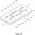
- FIG. 21is a perspective view of main portions of a waveguide slot array antenna according to a third embodiment of the present disclosure
- FIG. 22is a structural view of an internal signal waveguide path of the waveguide slot array antenna shown in FIG. 21 , showing an example of a basic structure in which excitation slots are arranged in a minimum array unit (e.g., 6 ⁇ 2).
- a minimum array unite.g. 6 ⁇ 2
- the waveguide slot array antenna according to the third embodiment of the present disclosurelike the structure shown in FIGs.
- 19 and 21may include a feeding plate 41, a distribution plate 42 which is installed stacked on the feeding plate 41 and has a feeding waveguide 412 and a waveguide structure for delivering a signal input through the feeding waveguide 412 to a radiation plate 43 through a coupling slot (not shown), and the radiation plate 43 which is installed stacked on the distribution plate 42 and has multiple first through twelfth excitation slots 432 (432-1, 432-2, 432-3 432-4, 432-5, 432-6 , 432-7, 432-8, 432-9, 432-10, 432-11, and 432-12) formed therein and a cavity structure 430 for distributing the signal input through the coupling slot of the distribution plate 42 and exciting the distributed signal through the excitation slots 432.
- auxiliary radiation plate(s)may be further installed on the radiation plate 43 to generate a polarized wave.
- the cavity structure 430 of the radiation plate 43is divided into four first through fourth regions a, b, c, and d for distributing the signal provided from the distribution plate 42, for example, equally, into four parts, and correspondingly, septums having a predetermined length are formed on and perpendicular to each surface of the cavity.
- septumshaving a predetermined length are formed on and perpendicular to each surface of the cavity.
- three excitation slotsare formed unlike in the structure shown in FIGs. 19 and 20 .
- the first through third excitation slots 432-1, 432-2, and 432-3are formed and are designed such that the centers thereof are offset from an array reference axis (e.g., a vertical axis) in opposite directions to that (those) of the adjacent excitation slot(s).
- an array reference axise.g., a vertical axis
- such an array structure of the excitation slotsenables a strength of a signal provided to each excitation slot to be as strong as possible and to be equally distributed.
- the third through sixth excitation slots 432-4, 432-5, and 432-6are formed in the second region b
- the seventh through ninth excitation slots 432-7, 432-8, and 432-9are formed in the third region c
- the tenth through twelfth excitation slots 432-10, 432-11, and 432-12are formed in the fourth region d.
- the waveguide slot array antenna according to the second and third embodiments of the present disclosuremay provide flexibility to the design of the excitation slot array structure of the radiation plate when compared to a general array structure of the power of 2.
- an overall antenna structureimplements maximum directivity for an arbitrary size and maintains a low-profile structure as a whole.
- the waveguide slot array antenna having various array structuresmay be easily implemented.
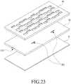
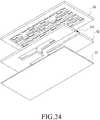
- FIG. 23is an exploded perspective view of main portions of a waveguide slot array antenna according to a fourth embodiment of the present disclosure, viewed from a side (e.g., a top side),
- FIG. 24is an exploded perspective view of the waveguide slot array antenna of FIG. 23 , viewed from another side (e.g., a bottom side)
- FIGs. 25 and 26are perspective views of a radiation plate 53 of FIG. 23 , viewed from a side and another side, respectively
- FIGs. 27 and 28are perspective views of a distribution plate 52 of FIG. 23 , viewed from a side and another side, respectively, in which excitation slots have an array structure of, for example, 10 ⁇ 4 (length ⁇ width).
- the waveguide slot array antennamay include a feeding plate 51, a distribution plate 52 which is installed stacked on the feeding plate 51 and has a feeding waveguide 512 and a distribution waveguide structure for equally or unequally distributing and delivering a signal input through the feeding waveguide 512 to the radiation plate 53 through multiple coupling slots 522 designed to be, for example, a power of 2, and the radiation plate 53 which is installed stacked on the distribution plate 52 and has excitation slots formed therein and a cavity structure for distributing the signal input through the multiple coupling slots 522 of the distribution plate 52 and exciting the distributed signal through the excitation slots.
- auxiliary radiation plate(s)may be further installed on the radiation plate 53 to generate a polarized wave.
- the radiation plate 53 according to the fourth embodiment of the present disclosureis structured by repeatedly using and properly arranging and connecting the radiation plates according to the other preceding embodiments.
- the radiation plate 53 having a 10 ⁇ 4 array structureis structured such that a 4 ⁇ 2 minimum array unit structure according to the second embodiment shown in FIGs. 19 and 20 is applied to two regions, e.g., the region a and the region c (thus forming, e.g., a 4 ⁇ 4 array structure) and a 6 ⁇ 2 minimum array unit structure according to the third embodiment shown in FIGs.
- the radiation plate 53 shown in FIG. 23is implemented by applying a total of four minimum array unit structures including two minimum array unit structures according to the second embodiment and two minimum array unit structures according to the fourth embodiment, and in this case, the distribution plate 52 has a structure for equally or unequally distributing an input signal to each of the four minimum array unit structures.
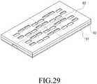
- FIG. 29is a perspective view of main portions of a waveguide slot array antenna according to a fifth embodiment of the present disclosure, in which excitation slots have, for example, an 8 ⁇ 4 (length ⁇ width) array structure.
- the waveguide slot array antenna according to the fifth embodiment of the present disclosureis structured such that a feeding plate 61, a distribution plate 62, and a radiation plate 63 are sequentially stacked in that order, like in the structure according to the fourth embodiment shown in FIGs. 23 through 28 .
- the radiation plate 63 having the 8 ⁇ 4 array structuremay be implemented by using and connecting four 4 ⁇ 2 minimum array unit structures according to the second embodiment shown in FIGs. 19 and 20 .
- FIG. 30is a perspective view of main portions of a waveguide slot array antenna according to a sixth embodiment of the present disclosure, in which excitation slots have, for example, an 10 ⁇ 8 (length ⁇ width) array structure.
- the waveguide slot array antenna according to the sixth embodiment of the present disclosureis structured such that a feeding plate 71, a distribution plate 72, and a radiation plate 73 are sequentially stacked in that order, like in the structure according to the fourth embodiment shown in FIGs. 23 through 28 .
- the radiation plate 73 having the 10 ⁇ 8 array structure shown in FIG. 30may be implemented by using and connecting four 4 ⁇ 2 minimum array unit structures according to the second embodiment shown in FIGs. 19 and 20 and four 6 ⁇ 2 minimum array unit structures according to third embodiment shown in FIGs. 21 and 22 .
- the auxiliary radiation plate(s) according to the present disclosuremay be applied to waveguide slot array antennas with various structures having radiation slot arrays as well as the described structures. That is, in the waveguide slot array antennas having various structures, like in the structure according to the first embodiment of the present disclosure, first and second auxiliary radiation plates in which first and second polarization slots are formed correspondingly to a radiation slot array may be installed to generate a polarized wave.
- a plurality of minimum array unit structures according to the second and third embodimentsare used for extended array structures according to the fourth through sixth embodiments as an example in the foregoing description, a plurality of minimum array unit structures according to the second and third embodiments may be used to properly implement other array structures.
- a feeding waveguideis formed on a distribution plate as an example, but like in the structure according to the first embodiment, a structure in which a feeding slot is formed in a feeding plate may also be adopted.
Landscapes
- Variable-Direction Aerials And Aerial Arrays (AREA)
- Waveguide Aerials (AREA)
Description
- The present disclosure relates to a super high frequency transmitting and receiving antenna, and more particularly, to a waveguide slot array antenna.
- Super high frequency transmitting and receiving antennas include a parabolic-type antenna, a microstrip antenna, a waveguide slot array antenna, and so forth. Among these antennas, a microstrip array antenna or a waveguide slot array antenna is mainly used for miniaturization through thickness reduction.
- The microstrip array antenna has a microstrip patch array structure using a dielectric substrate, in which a loss of a transmitted or received signal is large depending on a loss coefficient of a dielectric based on characteristics of the dielectric substrate, and an ohmic loss of a conductor occurs, and the loss increases especially for a higher frequency, such that the use of the microstrip array antenna is avoided in a super high frequency band.
- The waveguide slot array antenna has a structure in which a hole in the form of a slot is formed in a general waveguide, without using the dielectric substrate. Generally, a waveguide is a hollow metal pipe and a sort of high pass filter in which a guided mode has a specific cutoff frequency and a dominant mode is determined by a size of the waveguide. The waveguide has lower attenuation than a parallel two-wire line, a coaxial cable, etc., and thus is mostly used for high power in a microwave transmission line. The waveguide may have various cross-sectional shapes, depending on which the waveguide is classified into a circular waveguide, a quadrangular waveguide, an oval waveguide, and so forth.
- Techniques related to the waveguide slot array antenna are disclosed in, for example, a Korean Patent Application No.
2006-18147 2007-7000182 FIG. 1A is a perspective view in which each layer of a conventional waveguide slot array antenna having a stacked multi-layer structure is partially cut. Referring toFIG. 1A , the conventional waveguide slot array antenna includes afeeding plate 11 in which aninput feeding slot 112 is formed, adistribution plate 12 which is installed on thefeeding plate 11 and in which a distributor andcoupling slots 122 are formed, amain radiation plate 13 which is installed on thedistribution plate 12 and in which a cavity structure and an excitation slot (or a radiation slot) 132 are formed, and anauxiliary radiation plate 14 which is installed on themain radiation plate 13 and in which apolarization slot 142 is formed to generate a polarized wave having a polarization plane inclined at 45 degrees(°).- Once a signal is input from the
feeding slot 112 of thefeeding plate 11, the input signal is distributed, for example, in an equal ratio, through thedistribution plate 12, and each distributed signal is delivered to each cavity formed in themain radiation plate 13 through thecoupling slots 122. The signal delivered to the cavity of themain radiation plate 13 is distributed and radiated in an equal ratio through, for example, fourexcitation slots 132 formed for each cavity. Theexcitation slots 132 are arranged to have a preset interval and preset arrangement therebetween according to an operating frequency. - In the
auxiliary radiation plate 14 installed on themain radiation plate 13, thepolarization slots 142, each of which one-to-one corresponds to eachexcitation slot 132 of themain radiation plate 13, is formed, and the signal delivered to thepolarization slot 142 is rotated at 45 degrees when compared to radiation from theexcitation slot 132 and is radiated to the space. That is, a wave polarized at 45 degrees in a vertical/horizontal direction is generated by theauxiliary radiation plate 14. Referring to a slot shape of theexcitation slot 132, theexcitation slot 132 has, for example, an approximately rectangular shape, and is formed in an erect position or posture in the vertical/horizontal direction, and for a slot shape of thepolarization slot 142, thepolarization slot 142 has a rectangular shape similar to the approximately rectangular shape of theexcitation slot 132, but when compared to the slot shape of theexcitation slot 132, the rectangular shape of thepolarization slot 142 is formed in a position or posture mechanically rotated at 45 degrees in the vertical/horizontal direction and thus may be globally similar to a diamond shape. Such a structure may be regarded as a structure that forms one radiation slot by a combination of theexcitation slot 132 and thepolarization slot 142. - As such, to operate the conventional waveguide slot array antenna for vertical/horizontal polarization, the
auxiliary radiation plate 14 is used and thepolarization slot 142 of theauxiliary radiation plate 14 may have a rectangular shape rotated at 45 degrees with respect to theexcitation slot 132 to rotate a polarization plane of a signal radiated from theexcitation slot 132 at 45 degrees. With this structure, a side lobe component is significantly suppressed by a total length of a vertical/horizontal plane. - However, as the
rectangular polarization slot 142 formed in theauxiliary radiation plate 14 is rotated at 45 degrees in the vertical/horizontal direction to have a shape similar to the diamond shape, an arrangement interval between thepolarization slots 142 on the vertical/horizontal plane may fail to satisfy a proper distance criterion required when a wavelength of an operating frequency is considered. That is, as indicated by a inFIG. 1A , a distance, especially between thepolarization slots 142 arranged diagonally to each other may increase. Such a structure may cause a grating lobe. - More specifically, in an array antenna, if a distance between arrays exceeds one wavelength, a specific radiation angle is produced at which signals radiated from respective radiation slots are in phase. A lobe produced in this case is called a grating lobe that is a sort of main lobe. The grating lobe is generated by a phase of an array element in the array antenna, and the phase is controlled by a distance between elements.
FIG. 1B shows a state in which a main lobe and a grating lobe are produced, for example, in positions P1 and P2 of two polarization slots located diagonally (having a distance of d therebetween) inFIG. 1A . Referring toFIG. 1B , when a phase difference between two paths is one wavelength λ, the grating lobe is produced at an angle rotated by θ from the main lobe. The generated angle may be simply expressed with the following equation.
- Due to the grating lobe, radiation pattern envelope (RPE) standards prescribed in corresponding countries may not be satisfied. Thus, a scheme for suppressing the grating lobe is required.
US 6,028,562 A1 discloses an antenna comprising a planar array of waveguide slot radiators for communicating electromagnetic signals exhibiting simultaneous dual polarization states. The antenna consists of parallel waveguides of rectangular or ridged cross section. The broadwalls of each parallel waveguide contain a linear array of input slots for receiving or transmitting electromagnetic signals having a first polarization state from/to the parallel waveguide and for transmitting or receiving those signals into/from an array of cavity sections. The cavity sections comprise a short section of uniform waveguide with a length of much less than a wavelength in the propagation direction. The cavity sections feed to output slots which are rotated relative to the input slots.KR 100 721 871 B1 - It may be possible to suppress the grating lobe by disposing multiple excitation slots on an identical antenna area where an arrangement interval between excitation slots is reduced, but in a conventional structure, the number of excitation slot arrays increases to a power of 2 depending on a distribution plate and a cavity structure that distributes a signal on a main radiation plate, showing some limitations in the design of arrangement of excitation slots.
- The present disclosure is proposed to solve the foregoing problems, and provides a waveguide slot array antenna that generates a polarized wave while effectively suppressing a grating lobe.
- The present disclosure also provides a waveguide slot array antenna that freely implements an overall antenna structure by improving the degree of freedom as to the design of a slot array.
- The above objects are solved by the claimed matter according to the independent claim.
- The first auxiliary radiation plate may include an array of first polarization slots formed to have a structure corresponding to the excitation slot array of the main radiation plate, and the first polarization slots may be structured to rotate a polarization plane of a signal radiated by a corresponding excitation slot.
- The second auxiliary radiation plate may include an array of a plurality of second polarization slots formed for each first polarization slot of the first auxiliary radiation plate, and a distribution structure for distributing a signal radiated for each first polarization slot of the first auxiliary radiation plate to the plurality of second polarization slots corresponding to the first polarization slot is formed in the second auxiliary radiation plate.
- The waveguide slot array antenna may further include a feeding plate which forms at least a part of a waveguide to be provided with an input signal and a distribution plate which includes a distribution waveguide structure coupled to the feeding plate to distribute the input signal to multiple coupling slots, in which the main radiation plate is installed on the distribution plate and includes multiple cavity structures for distributing a signal input through each coupling slot of the distribution plate in an equal ratio and exciting the distributed signal through the excitation slot array
- As described above, the waveguide slot array antenna according to the invention generates a polarized wave while effectively suppressing a grating lobe, thereby reducing an influence upon an adjacent device in an adjacent-fixed communication device.
- Moreover, the waveguide slot array antenna according to the invention may improve the degree of freedom as to the design of slot arrangement, allowing free implementation of an overall antenna structure. Hence, the unnecessary increase of the antenna size may be prevented, and processing complexity may be reduced by maintaining a proper arrangement level, thereby reducing a loss of time cost.
FIG. 1A is a perspective view in which each layer of a conventional waveguide slot array antenna is partially cut;
antenna is partially cut according to a first embodiment of the present disclosure;FIG. 3 is a perspective view of a side of a second auxiliary radiation plate shown inFIG. 2 ;FIG. 4 is a perspective view of another side of a second auxiliary radiation plate shown inFIG. 2 ;FIG. 5 is a perspective view showing a connection relationship between a second polarization slot of a second auxiliary radiation plate and a first polarization slot of a first auxiliary radiation plate inFIG. 2 ;FIG. 6 is a side structural view showing a connection relationship between a second polarization slot of a second auxiliary radiation plate and a first polarization slot of a first auxiliary radiation plate inFIG. 2 ;FIG. 7 is a side structural view showing a connection relationship in a modified structure between a second polarization slot of a second auxiliary radiation plate and a first polarization slot of a first auxiliary radiation plate inFIG. 2 ;FIG. 8 is a perspective view of a side of a first auxiliary radiation plate shown inFIG. 2 ;FIG. 9 is a perspective view of a radiation plate ofFIG. 2 in a side direction;FIG. 10 is a perspective view of a radiation plate ofFIG. 2 in another side direction;FIG. 11 is a perspective view of a distribution plate ofFIG. 2 in a side direction;FIG. 12 is a perspective view of a distribution plate ofFIG. 2 in another side direction;FIG. 13 is a plane view of a feeding plate shown inFIG. 2 ;FIG. 14 is a structural view of an internal signal waveguide path of a waveguide slot array antenna according to the first embodiment of the present disclosure;FIG. 15 is a graph showing grating lobe characteristics of the waveguide slot array antenna shown inFIG. 14 ;FIG. 16 is a graph showing cross polarization characteristics of a waveguide slot array antenna shown inFIG. 14 ;FIG. 17 is a perspective view of main portions of a waveguide slot array antenna for comparison with embodiments of the present disclosure;FIG. 18 is a structural view of an internal signal waveguide path of a waveguide slot array antenna shown inFIG. 17 ;FIG. 19 is a perspective view of main portions of a waveguide slot array antenna according to a second embodiment of the present disclosure;FIG. 20 is a structural view of an internal signal waveguide path of a waveguide slot array antenna shown inFIG. 19 ;FIG. 21 is a perspective view of main portions of a waveguide slot array antenna according to a third embodiment of the present disclosure;FIG. 22 is a structural view of an internal signal waveguide path of a waveguide slot array antenna shown inFIG. 21 ;FIG. 23 is an exploded perspective view of main portions of a waveguide slot array antenna according to a fourth embodiment of the present disclosure, viewed from a side;FIG. 24 is an exploded perspective view of a waveguide slot array antenna ofFIG. 23 , viewed from another side;FIG. 25 is a perspective view of a radiation plate ofFIG. 23 , viewed from a side;FIG. 26 is a perspective view of a radiation plate ofFIG. 23 , viewed from another side;FIG. 27 is a perspective view of a distribution plate ofFIG. 23 , viewed from a side;FIG. 28 is a perspective view of a distribution plate ofFIG. 23 , viewed from another side;FIG. 29 is a perspective view of main portions of a waveguide slot array antenna according to a fifth embodiment of the present disclosure; and from another side;FIG. 29 is a perspective view of main portions of a waveguide slot array antenna according to a fifth embodiment of the present disclosure; andFIG. 30 is a perspective view of main portions of a waveguide slot array antenna according to a sixth embodiment of the present disclosure.- Hereinafter, exemplary embodiments of the present disclosure will be described in detail with reference to the accompanying drawings. In the following description, specific details such as detailed elements, etc., will be provided, but they are merely provided to help the overall understanding of the present disclosure.
FIG. 2 is a perspective view in which each layer of a waveguide slot array antenna having a stacked multi-layer structure is partially cut according to a first embodiment of the present disclosure. Referring toFIG. 2 , the waveguide slot array antenna according to the first embodiment of the present disclosure, like a conventional waveguide slot array antenna, may include afeeding plate 11 in which aninput feeding slot 112 is formed, adistribution plate 12 which is installed on thefeeding plate 11 and has a distributor and acoupling slot 122 formed therein, and amain radiation plate 13 which is installed on thedistribution plate 12 and has a cavity structure and an excitation slot (or a radiation slot) 132 formed therein. According to characteristics of the present disclosure, the waveguide slot array antenna may further include a first auxiliary radiation plate which is installed on themain radiation plate 13 and has afirst polarization slot 142 formed therein to generate a polarized wave having a polarization plane inclined at 45 degrees and a secondauxiliary radiation plate 15 which is installed on the firstauxiliary radiation plate 14 and has asecond polarization slot 152 input through thefeeding slot 112 of thefeeding plate 11, the input signal is distributed in an equal ratio through thedistribution plate 12, and each distributed signal is delivered to each cavity formed in themain radiation plate 13 through thecoupling slots 122. The signal delivered to the cavity of themain radiation plate 13 is distributed and radiated, for example, in an equal ratio through, for example, fourexcitation slots 132 formed for each cavity. Theexcitation slots 132 are arranged to have a preset interval and preset arrangement therebetween according to an operating frequency.- In the first
auxiliary radiation plate 14 installed on themain radiation plate 13, like in the conventional waveguide slot array antenna, thefirst polarization slots 142 are formed to one-to-one correspond to therespective excitation slots 132 of themain radiation plate 13. Thefirst polarization slot 142 is structured such that an approximately quadrangular (or rectangular) slot is formed in a posture mechanically rotated at 45 degrees with respect to theexcitation slot 132. With this structure, for the signal delivered to thefirst polarization slot 142, a polarized wave signal is generated to have a polarization plane rotated at 45 degrees relative to the signal radiated from theexcitation slot 132. - According to the first embodiment of the present disclosure, in the second
auxiliary radiation plate 15 installed on the firstauxiliary radiation plate 14, a plurality of (e.g., two)second polarization slots 152 are formed to correspond to eachfirst polarization slot 142 of the firstauxiliary radiation plate 14 and a distribution structure for distributing a signal to the plurality of correspondingsecond polarization slots 152 for eachfirst polarization slot 142 is formed. Shapes (and postures) of thefirst polarization slot 142 and the plurality ofsecond polarization slots 152 may be the same as one another. With this structure, the polarized wave generated in thefirst polarization slot 142 is distributed and radiated through thesecond polarization slots 152. - It can be seen that as a whole, the first
auxiliary radiation plate 14 and the secondauxiliary radiation plate 15 further include a structure for rotating a signal excited by theexcitation slot 132 of themain radiation plate 13 such that the signal has a polarization plane inclined at 45 degrees and an extended slot array structure using an electric field plane or magnetic field plane signal distribution structure. FIG. 3 is a perspective view of a top side (e.g., a front side along a signal radiation direction) of the secondauxiliary radiation plate 15,FIG. 4 is a perspective view of a bottom side (e.g., a rear side along the signal radiation direction) of the secondauxiliary radiation plate 15, andFIGs. 5 and6 are a perspective view and a side view showing a connection relationship between thesecond polarization slot 152 of the secondauxiliary radiation plate 15 and thefirst polarization slot 142 of the firstauxiliary radiation plate 14, respectively. To be more specific regarding structures and operations of the secondauxiliary radiation plate 15 and thesecond polarization slot 152 with reference toFIGs. 3 through 6 , an electric field of a signal delivered from theexcitation slot 132 of themain radiation plate 13 is fixed after rotated at 45 degrees in thefirst polarization slot 142 of the firstauxiliary radiation plate 14, and then the signal is delivered toward thesecond polarization slot 152 of the secondauxiliary radiation plate 15.- The signal delivered to the second
auxiliary radiation plate 15 is distributed through the distribution structure formed under thesecond polarization slots 152, such that each distributed signal is provided to the plurality ofsecond polarization slots 152. Such a distribution structure may have a structure branched vertically or horizontally with respect to an electric field plane. The signal distributed and provided to thesecond polarization slot 152 is radiated to the space and thus may be expressed in an overall antenna radiation pattern. - When viewed from a top side of the second
auxiliary radiation plate 15, an arrangement interval between thesecond polarization slots 152 may be, for example, a half of an arrangement interval between thefirst polarization slots 142 of the firstauxiliary radiation plate 14 according to a branched plane. That is, with this structure, an arrangement interval on a vertical/horizontal plane between thesecond polarization slots 152 formed in the secondauxiliary radiation plate 15 may sufficiently satisfy a criterion of within one wavelength with respect to an operating frequency, thus sufficiently suppressing a grating lobe. FIG. 7 is a perspective view showing a modified structure of thesecond polarization slot 152 of the secondauxiliary radiation plate 15 and thefirst polarization slot 142 of the firstauxiliary radiation plate 14 inFIG. 2 . Referring to the modified structure shown inFIG. 7 , a second polarization slot 152-1 is formed in the secondauxiliary radiation plate 15 without a distribution structure under thesecond polarization slot 152; instead, the distribution structure is formed above a first polarization slot 142-1 of the firstauxiliary radiation plate 14. That is, in the modified structure shown inFIG. 7 , the second polarization slot 152-1 is formed in the secondauxiliary radiation plate 15, and the firstauxiliary radiation plate 14 has the first polarization slot 142-1 and the distribution structure formed above the first polarization slot 142-1.- When the first
auxiliary radiation plate 14 and the secondauxiliary radiation plate 15 are coupled to each other, a shape of a waveguide path formed by the first polarization slot 142-1, the distribution structure, and the second polarization slot 152-1 to deliver an internal signal therethrough is substantially the same as a shape of a waveguide path formed by the structure shown inFIGs. 2 through 6 , and signal delivery characteristics are identical. FIG. 8 is a perspective view of a side of the firstauxiliary radiation plate 14 shown inFIG. 2 ,FIG. 9 is a perspective view of a top side (e.g., a front side along a signal radiation direction) of theradiation plate 13 shown inFIG. 2 ,FIG. 10 is a perspective view of a bottom side (e.g., a rear side in the signal radiation direction) of theradiation plate 13 shown inFIG. 2 ,FIGs. 11 and12 are perspective views of a top side and a side of thedistribution plate 12 shown inFIG. 2 , andFIG. 13 is a plane view of thefeeding plate 11 shown inFIG. 2 . Referring toFIGs. 8 through 12 , a basic structure and operations of a waveguide slot array antenna will be described in more detail.FIGs. 8 through 12 are views according to an order in which plates are installed from a top side to a bottom side, but the following description will be made based on signal input and a waveguiding path.- First, a waveguide (not shown) for guiding a signal input through an input connector (not shown), etc., is formed in a proper shape on a side with respect to a bottom surface of the
feeding plate 11. The bottom surface of thefeeding plate 11 may be formed to be, for example, several millimeters to several tens of millimeters. Thefeeding slot 112 is formed at a terminal of the waveguide of thefeeding plate 11, and thefeeding slot 112 may be a multistage slot to achieve matching according to a size of a distribution waveguide formed on thecorresponding distribution plate 12. The rear surface of thefeeding plate 11 may be processed to have a hole or a tab corresponding to an engagement portion of a normalized waveguide flange. - The
distribution plate 12 connected with the feedingpate 11 has a distribution waveguide structure for distributing a signal input through thefeeding slot 112 of thefeeding plate 11 to themultiple coupling slots 122. The number of branched final branches of the distribution waveguide structure corresponds to distribution into a power of 2, and the branches are top-bottom and left-right symmetric. Such a distribution waveguide structure may have an electric field or magnetic field distribution structure. The electric field or magnetic field distribution structure may further include an iris structure and a septum structure, taking matching characteristics into account. In the distribution waveguide structure, thecoupling slot 122 is formed at a terminal of each branched final branch. Thecoupling slot 122 is located one-sidedly by being offset from the center of a waveguide structure at the terminal of each final branch of the distribution waveguide structure, causing strong coupling. Themain radiation plate 13 connected with thedistribution plate 12 distributes a signal input through eachcoupling slot 122 of thedistribution plate 12 in an equal or unequal ratio, and has a cavity structure for exciting the distributed signal through eachexcitation slot 132. Eachcoupling slot 122 of thedistribution plate 12 is designed to be located in the center of a corresponding cavity of themain radiation plate 13. Each cavity may be structured to have, for example, fourexcitation slots 132 formed therein, and to properly form a resonance condition of each of the fourexcitation slots 132, a septum having a predetermined length is formed on and perpendicular to each surface of the cavity. - As shown in
FIGs. 8 through 12 , the feedingplate 11, thedistribution plate 12, and themain radiation plate 13 may be designed, and the firstauxiliary radiation plate 14 and the secondauxiliary radiation plate 15 are designed correspondingly thereto. The feedingplate 11, thedistribution plate 12, themain radiation plate 13, the firstauxiliary radiation plate 14, and the secondauxiliary radiation plate 15 are also aligned and mutually coupled to one another according to a designed structure. In this case, coupling between the plates may use screw engagement using a screw, soldering, high-frequency welding, or the like. FIG. 14 is a structural view of (a part of) an internal signal waveguide path of the waveguide slot array antenna according to the first embodiment of the present disclosure, in which a structure according to some embodiments of the present disclosure is shown in (b) ofFIG. 14 , and an internal signal waveguide path (or a part thereof) of the conventional waveguide slot array antenna as shown inFIG. 1 is shown in (a) ofFIG. 14 for comparison.FIG. 15 is a graph showing grating lobe characteristics of the waveguide slot array antenna shown inFIG. 14 , andFIG. 16 is a graph showing cross polarization characteristics of the waveguide slot array antenna shown inFIG. 14 . InFIG. 16 , a graph of characteristics according to the first embodiment of the present disclosure is shown in (b), and a graph of characteristics of the conventional waveguide slot array antenna as shown inFIG. 1 is shown in (a) for comparison.- Referring to
FIGs. 14 through 16 , a waveguide slot array antenna according to the present disclosure may be regarded as further including the secondauxiliary radiation plate 15 when compared to a conventional waveguide slot array antenna, and although one layer (plate) is physically further stacked, an overall height of the antenna may be the same as that of the conventional antenna. That is, as shown inFIG. 14 , an overall height h1 of the conventional antenna and an overall height h2 of the antenna according to the present disclosure may be equal to each other. In such a design, as shown inFIG. 15 , grating lobe characteristics of the antenna according to the present disclosure are further improved in spite of primary and secondary side lobes having sizes equal to those of the conventional antenna. - In the waveguide slot array antenna, a height of a radiation slot at a final stage dominantly works as a determinant of cross polarization. As shown in
FIG. 14 , a height h21 of a radiation slot (a second polarization slot) at a final stage of the antenna according to the present disclosure is designed to be smaller than a height h11 of a radiation slot (a first polarization slot) at a final stage of the conventional antenna. This results from the design in which the overall height of the antenna according to the present disclosure is equal to that of the conventional antenna, and it can be seen fromFIG. 16 that even in such a design, there is no deterioration of cross polarization characteristics. Moreover, generally, a larger difference between co-polarization and cross polarization is regarded as more excellent performance, and as shown inFIG. 16 , it can be seen that the cross polarization characteristics of the antenna according to the present disclosure are significantly improved. In this way, the present disclosure may optimally design the height of the radiation slot at the final stage of the antenna. FIG. 17 is a perspective view of main portions of a waveguide slot array antenna for comparison with embodiments of the present disclosure, andFIG. 18 is a structural view of an internal signal waveguide path of the waveguide slot array antenna shown inFIG. 17 . The waveguide slot array antenna shown inFIGs. 17 and 18 may basically include a structure in which thefeeding plate 21, thedistribution plate 22, and theradiation plate 23 are sequentially stacked in that order, like the structure according to the first embodiment shown inFIG. 2 and other drawings. Although not shown inFIGs. 17 and 18 , auxiliary radiation plate(s) may be further installed on theradiation plate 23 to generate a polarized wave, similarly with the structure shown inFIG. 2 and other drawings.- In the structuure shown in
FIG. 2 and other drawings, a structure for providing an input signal through a feeding slot of a feeding plate is desclosed as an example, but inFIGs. 17 and 18 , a structure for providing an input signal through a feedingwaveguide 212 having an open section for signal input formed in a side of thedistribution plate 22 is shown as an example. Thedistribution plate 22 forms the feedingwaveguide 212 and a hollow region of a distribution waveguide structure for distributing a signal input through the feedingwaveguide 212, and thefeeding plate 21 may simply have the form of a flat plate. - In the structure shown in
FIGs. 17 and 18 , if a signal is input to thefeeding waveguide 212, the signal is distributed in an equal ratio through thedistribution plate 22 and the distributed signal is delivered to eachcavity 220 formed in theradiation plate 23. The signal delivered to thecavity 220 of theradiation plate 23 is distributed and radiated, for example, in an equal ratio through, for example, fourexcitation slots 232 formed for eachcavity 220. Theexcitation slots 232 are arranged to have a preset interval and preset arrangement therebetween according to an operating frequency. - As shown in
FIGs. 17 and 18 , generally, in a waveguide slot array antenna (and other planar antennas), an input signal is distributed into a power of 2, for example, equally, in thedistribution plate 22, and the signal distributed and then finally radiated through theexcitation slot 232 in theradiation plate 23 is distributed into a power of 2, such that theexcitation slots 232 are arranged in the form of a power of 2, such as 2×2, 4×4, or the like. For example, in theradiation plate 23 shown inFIGs. 17 and 18 , a signal that is input through one coupling slot of thedistribution plate 22 and delivered to one cavity of theradiation plate 23 is radiated through fourexcitation slots 232 formed for each cavity. Thus, this structure has an array of a total of 4×4, 8×8, 16×16, etc.excitation slots 232. - As such, generally, in the waveguide slot array antenna, a signal distribution structure uses an H-junction structure, thereby implementing a symmetric and efficient feeding network structure. However, due to such a structure, there are a limitation in horizontal and vertical beam patterns, a difficulty in the flexible design of a gain, and an unnecessarily large volume. Moreover, according to circumstances, in case of an asymmetric structure array design, the H-junction structure is not easy to adopt and a separate additional layer may be needed for implementation of a desired structure array, increasing an overall thickness and thus limiting a low-profile design.
- In the structure of the radiation plate shown in
FIGs. 17 and 18 , an arrangement interval between excitation slots may be narrowed when compared to in other embodiments shown inFIG. 2 and other drawings, and thus, according to circumstances, when the first auxiliary radiation plate as shown inFIG. 2 is provided, a grating lobe may be suppressed without a need for the separate second auxiliary radiation plate on the first auxiliary radiation plate. FIG. 19 is a perspective view of main portions of a waveguide slot array antenna according to a second embodiment of the present disclosure, andFIG. 20 is a structural view of an internal signal waveguide path of the waveguide slot array antenna shown inFIG. 19 , showing an example of a basic structure in which excitation slots are arranged in a minimum array unit (e.g., 4×2). Referring toFIGs. 19 and 20 , the waveguide slot array antenna according to the second embodiment of the present disclosure, like the structure shown inFIGs. 17 and 18 , may include afeeding plate 31, adistribution plate 32 which is installed stacked on thefeeding plate 31 and has afeeding waveguide 312 and a waveguide structure for delivering a signal input through the feedingwaveguide 312 to aradiation plate 33 through a coupling slot (not shown), and theradiation plate 33 which is installed stacked on thedistribution plate 32 and has multiple first through eighth excitation slots 332 (332-1, 332-2, 332-3 332-4, 332-5, 332-6 , 332-7, and 332-8) formed therein and acavity structure 330 which distributes the signal input through the coupling slot of thedistribution plate 32 and excites the distributed signal through the excitation slots 332. Although not shown inFIGs. 18 and19 , auxiliary radiation plate(s) may be further installed on theradiation plate 33 to generate a polarized wave.- To be more specific regarding the structure of the
radiation plate 33, thecavity structure 330 of theradiation plate 33 is divided into four first through fourth regions a, b, c, and d for distributing the signal provided from thedistribution plate 32, for example, equally, into four parts, and correspondingly, septums having a predetermined length are formed on and perpendicular to each surface of the cavity. In each of the four regions a, b, c, and d of thecavity structure 330, two excitation slots are formed unlike in the structure shown inFIGs. 17 and 18 . For example, in thecavity structure 330, in the first region a, the first and second excitation slots 332-1 and 332-2 may be formed and designed such that the centers thereof are offset from an array reference axis (e.g., a vertical axis) in opposite directions to each other. Such an array structure of the excitation slots enables a strength of a signal provided to each excitation slot to be as strong as possible and to be equally distributed. Likewise, the third and fourth excitation slots 332-3 and 332-4 may be formed in the second region b, the fifth and sixth excitation slots 332-5 and 332-6 may be formed in the third region c, and the seventh and eighth excitation slots 332-7 and 332-8 may be formed in the fourth region d. - In the structure shown in
FIGs. 19 and 20 , it can be seen that thedistribution plate 32 merely delivers the signal input through the feedingwaveguide 312 to theradiation plate 33 through one coupling slot, without actually distributing the signal. This is because the excitation slot array structure shown inFIGs. 19 and 20 is shown as having a minimum array unit of, e.g., 4×2 (width × length) for convenience of a description. It would be understood that when such a minimum array unit structure is repeatedly provided, thedistribution plate 32 may distribute the input signal through repeatedly provided minimum array unit structures. FIG. 21 is a perspective view of main portions of a waveguide slot array antenna according to a third embodiment of the present disclosure, andFIG. 22 is a structural view of an internal signal waveguide path of the waveguide slot array antenna shown inFIG. 21 , showing an example of a basic structure in which excitation slots are arranged in a minimum array unit (e.g., 6×2). Referring toFIGs. 21 and22 , the waveguide slot array antenna according to the third embodiment of the present disclosure, like the structure shown inFIGs. 19 and21 , may include afeeding plate 41, adistribution plate 42 which is installed stacked on thefeeding plate 41 and has afeeding waveguide 412 and a waveguide structure for delivering a signal input through the feedingwaveguide 412 to aradiation plate 43 through a coupling slot (not shown), and theradiation plate 43 which is installed stacked on thedistribution plate 42 and has multiple first through twelfth excitation slots 432 (432-1, 432-2, 432-3 432-4, 432-5, 432-6 , 432-7, 432-8, 432-9, 432-10, 432-11, and 432-12) formed therein and acavity structure 430 for distributing the signal input through the coupling slot of thedistribution plate 42 and exciting the distributed signal through the excitation slots 432. In addition, auxiliary radiation plate(s) may be further installed on theradiation plate 43 to generate a polarized wave.- To be more specific regarding the structure of the
radiation plate 43, thecavity structure 430 of theradiation plate 43 is divided into four first through fourth regions a, b, c, and d for distributing the signal provided from thedistribution plate 42, for example, equally, into four parts, and correspondingly, septums having a predetermined length are formed on and perpendicular to each surface of the cavity. In each of the four regions a, b, c, and d of thecavity structure 430, three excitation slots are formed unlike in the structure shown inFIGs. 19 and 20 . That is, in thecavity structure 430, in the first region a, the first through third excitation slots 432-1, 432-2, and 432-3 are formed and are designed such that the centers thereof are offset from an array reference axis (e.g., a vertical axis) in opposite directions to that (those) of the adjacent excitation slot(s). Needless to say, such an array structure of the excitation slots enables a strength of a signal provided to each excitation slot to be as strong as possible and to be equally distributed. Likewise, the third through sixth excitation slots 432-4, 432-5, and 432-6 are formed in the second region b, the seventh through ninth excitation slots 432-7, 432-8, and 432-9 are formed in the third region c, and the tenth through twelfth excitation slots 432-10, 432-11, and 432-12 are formed in the fourth region d. - As shown in
FIGs. 19 through 22 , the waveguide slot array antenna according to the second and third embodiments of the present disclosure may provide flexibility to the design of the excitation slot array structure of the radiation plate when compared to a general array structure of the power of 2. Thus, an overall antenna structure implements maximum directivity for an arbitrary size and maintains a low-profile structure as a whole. In particular, by properly applying the structures according to the second and third embodiments, the waveguide slot array antenna having various array structures may be easily implemented. FIG. 23 is an exploded perspective view of main portions of a waveguide slot array antenna according to a fourth embodiment of the present disclosure, viewed from a side (e.g., a top side),FIG. 24 is an exploded perspective view of the waveguide slot array antenna ofFIG. 23 , viewed from another side (e.g., a bottom side),FIGs. 25 and 26 are perspective views of aradiation plate 53 ofFIG. 23 , viewed from a side and another side, respectively, andFIGs. 27 and 28 are perspective views of adistribution plate 52 ofFIG. 23 , viewed from a side and another side, respectively, in which excitation slots have an array structure of, for example, 10×4 (length × width).- Referring to
FIGs. 23 through 28 , the waveguide slot array antenna according to the fourth embodiment, like the structure according to other embodiments, may include afeeding plate 51, adistribution plate 52 which is installed stacked on thefeeding plate 51 and has afeeding waveguide 512 and a distribution waveguide structure for equally or unequally distributing and delivering a signal input through the feedingwaveguide 512 to theradiation plate 53 throughmultiple coupling slots 522 designed to be, for example, a power of 2, and theradiation plate 53 which is installed stacked on thedistribution plate 52 and has excitation slots formed therein and a cavity structure for distributing the signal input through themultiple coupling slots 522 of thedistribution plate 52 and exciting the distributed signal through the excitation slots. In addition, auxiliary radiation plate(s) may be further installed on theradiation plate 53 to generate a polarized wave. - To be more specific regarding the structure of the
radiation plate 53, theradiation plate 53 according to the fourth embodiment of the present disclosure is structured by repeatedly using and properly arranging and connecting the radiation plates according to the other preceding embodiments. For example, as shown inFIG. 23 , theradiation plate 53 having a 10×4 array structure is structured such that a 4×2 minimum array unit structure according to the second embodiment shown inFIGs. 19 and 20 is applied to two regions, e.g., the region a and the region c (thus forming, e.g., a 4×4 array structure) and a 6×2 minimum array unit structure according to the third embodiment shown inFIGs. 21 and22 is applied to two regions, e.g., the region b and the region d (thus forming, e.g., a 6×4 array structure). That is, theradiation plate 53 shown inFIG. 23 is implemented by applying a total of four minimum array unit structures including two minimum array unit structures according to the second embodiment and two minimum array unit structures according to the fourth embodiment, and in this case, thedistribution plate 52 has a structure for equally or unequally distributing an input signal to each of the four minimum array unit structures. FIG. 29 is a perspective view of main portions of a waveguide slot array antenna according to a fifth embodiment of the present disclosure, in which excitation slots have, for example, an 8×4 (length × width) array structure. Referring toFIG. 29 , the waveguide slot array antenna according to the fifth embodiment of the present disclosure is structured such that afeeding plate 61, adistribution plate 62, and aradiation plate 63 are sequentially stacked in that order, like in the structure according to the fourth embodiment shown inFIGs. 23 through 28 .- In this case, as shown in
FIG. 29 , theradiation plate 63 having the 8×4 array structure may be implemented by using and connecting four 4×2 minimum array unit structures according to the second embodiment shown inFIGs. 19 and 20 . FIG. 30 is a perspective view of main portions of a waveguide slot array antenna according to a sixth embodiment of the present disclosure, in which excitation slots have, for example, an 10×8 (length × width) array structure. Referring toFIG. 30 , the waveguide slot array antenna according to the sixth embodiment of the present disclosure is structured such that afeeding plate 71, adistribution plate 72, and aradiation plate 73 are sequentially stacked in that order, like in the structure according to the fourth embodiment shown inFIGs. 23 through 28 .- In this case, the
radiation plate 73 having the 10×8 array structure shown inFIG. 30 may be implemented by using and connecting four 4×2 minimum array unit structures according to the second embodiment shown inFIGs. 19 and 20 and four 6×2 minimum array unit structures according to third embodiment shown inFIGs. 21 and22 . - The structure and operations of the waveguide slot array antenna according to the embodiments of the present disclosure may be as described above, and while the detailed embodiments have been described in the description of the present disclosure, various modifications may be made without departing from the scope of the present disclosure.
- For example, the detailed structures of the
feeding plate 11, thedistribution plate 12, and themain radiation plate 13 to which the auxiliary radiation plate(s) according to the first embodiment is applied have been described above, but the auxiliary radiation plate(s) according to the present disclosure may be applied to waveguide slot array antennas with various structures having radiation slot arrays as well as the described structures. That is, in the waveguide slot array antennas having various structures, like in the structure according to the first embodiment of the present disclosure, first and second auxiliary radiation plates in which first and second polarization slots are formed correspondingly to a radiation slot array may be installed to generate a polarized wave. - Although a plurality of minimum array unit structures according to the second and third embodiments are used for extended array structures according to the fourth through sixth embodiments as an example in the foregoing description, a plurality of minimum array unit structures according to the second and third embodiments may be used to properly implement other array structures.
- In addition, in the structures according to the second through sixth embodiments, a feeding waveguide is formed on a distribution plate as an example, but like in the structure according to the first embodiment, a structure in which a feeding slot is formed in a feeding plate may also be adopted.

Claims (9)
- A waveguide slot array antenna having an excitation slot (132, 232) array that radiates a signal corresponding to an operating frequency in a main radiation plate (13, 23), the waveguide slot array antenna comprising:a first auxiliary radiation plate (14) installed on the main radiation plate (13, 23), the first auxiliary radiation plate (14) comprising an array of first polarization slots (142) that are formed to one-to-one correspond to the respective excitation slots (132, 232) of the main radiation plate (13, 23), where the first polarization slot (142) is formed in a posture mechanically rotated with respect to the excitation slot (132, 232),characterized in thata second auxiliary radiation plate (15) installed on the first auxiliary radiation plate (14) where a plurality of second polarization slots (152) are formed to correspond to each first polarization slot (142) of the first auxiliary radiation plate (14) and where a distribution structure for distributing a signal to the plurality of corresponding second polarization slots (152) for each first polarization slot (142) is formed.
- The waveguide slot array antenna of claim 1, wherein the first auxiliary radiation plate (14) comprises an array of a first polarization slots (142) formed to have a structure corresponding to the excitation slot (132, 232) array of the main radiation plate (13, 23), and
the first polarization slots (142) are structured to rotate a polarization plane of a signal radiated by a corresponding excitation slot (132, 232). - The waveguide slot array antenna of claim 2, wherein the first polarization slot (142) has a slot shape that is similar to the excitation slot (132, 232), and the slot shape of the first polarization slot (142) is in a posture rotated at 45 degrees with respect to the slot shape of the excitation slot (132, 232) in a vertical/horizontal direction.
- The waveguide slot array antenna of claim 2, wherein the second auxiliary radiation plate (15) comprises an array of a plurality of second polarization slots (152) formed for each first polarization slot (142) of the first auxiliary radiation plate (14), and
a distribution structure for distributing a signal radiated for each first polarization slot (142) of the first auxiliary radiation plate (14) to the plurality of second polarization slots (152) corresponding to the first polarization slot (142) is formed in the second auxiliary radiation plate (15). - The waveguide slot array antenna of claim 3, wherein a shape of the first polarization slot (142) and a shape of the second polarization slot (152) are the same as each other.
- The waveguide slot array antenna of any one of claims 1 through 5, further comprising:a feeding plate (11, 21) which forms at least a part of a waveguide to be provided with an input signal; anda distribution plate (12, 22) which comprises a distribution waveguide structure coupled to the feeding plate (11, 21) to distribute the input signal to multiple coupling slots (122, 222),wherein the main radiation plate (13, 23) is installed on the distribution plate (12, 22) and comprises multiple cavity structures for distributing a signal input through each coupling slot (122, 222) of the distribution plate (12, 22) in an equal ratio and exciting the distributed signal through the excitation slot (132, 232) array.
- The waveguide slot array antenna of claim 6, wherein each of the multiple cavity structures of the main radiation plate (13, 23) are designed to be divided into four regions for distributing the signal provided to a corresponding coupling slot (122, 222) of the distribution plate (12, 22) to four parts, and a plurality of excitation slots (132, 232) are formed in each of the four regions.
- The waveguide slot array antenna of claim 7, wherein the plurality of excitation slots (132, 232) formed in each of the four regions of the cavity structure have centers that are offset from an array reference axis in opposite directions to a center of an adjacent excitation slot.
- The waveguide slot array antenna of claim 7, wherein the plurality of excitation slots (132, 232) are formed in each of the four regions of the cavity structure such that two or three excitation slots are formed in each of the four regions.
Applications Claiming Priority (3)
| Application Number | Priority Date | Filing Date | Title |
|---|---|---|---|
| KR20140156116 | 2014-11-11 | ||
| KR1020150077610AKR102302466B1 (en) | 2014-11-11 | 2015-06-01 | Waveguide slotted array antenna |
| PCT/KR2015/012036WO2016076595A1 (en) | 2014-11-11 | 2015-11-10 | Waveguide slot array antenna |
Publications (3)
| Publication Number | Publication Date |
|---|---|
| EP3220481A1 EP3220481A1 (en) | 2017-09-20 |
| EP3220481A4 EP3220481A4 (en) | 2018-09-26 |
| EP3220481B1true EP3220481B1 (en) | 2020-12-23 |
Family
ID=56103388
Family Applications (1)
| Application Number | Title | Priority Date | Filing Date |
|---|---|---|---|
| EP15858572.9AActiveEP3220481B1 (en) | 2014-11-11 | 2015-11-10 | Waveguide slot array antenna |
Country Status (7)
| Country | Link |
|---|---|
| US (2) | US10622726B2 (en) |
| EP (1) | EP3220481B1 (en) |
| JP (1) | JP6386182B2 (en) |
| KR (1) | KR102302466B1 (en) |
| CN (1) | CN107210533B (en) |
| CA (1) | CA2967279C (en) |
| ES (1) | ES2856056T3 (en) |
Families Citing this family (24)
| Publication number | Priority date | Publication date | Assignee | Title |
|---|---|---|---|---|
| KR102302466B1 (en)* | 2014-11-11 | 2021-09-16 | 주식회사 케이엠더블유 | Waveguide slotted array antenna |
| KR101698030B1 (en)* | 2015-10-01 | 2017-01-19 | 현대자동차주식회사 | antenna |
| US10559891B2 (en)* | 2016-03-15 | 2020-02-11 | Commscope Technologies Llc | Flat panel array antenna with integrated polarization rotator |
| US10490905B2 (en)* | 2016-07-11 | 2019-11-26 | Waymo Llc | Radar antenna array with parasitic elements excited by surface waves |
| US10539656B2 (en) | 2016-07-21 | 2020-01-21 | Waymo Llc | Antenna and radar system that include a polarization-rotating layer |
| EP4376219A3 (en)* | 2016-11-08 | 2024-10-23 | Robin Radar Facilities BV | A cavity slotted-waveguide antenna array and a method of manufacturing a cavity slotted-waveguide antenna array |
| CN106450748A (en)* | 2016-11-08 | 2017-02-22 | 广东盛路通信科技股份有限公司 | Cavity coupling slot radiation unit |
| CN107342454B (en)* | 2017-06-09 | 2020-02-21 | 宁波大学 | A waveguide slot array antenna |
| US10756417B2 (en)* | 2017-12-14 | 2020-08-25 | Waymo Llc | Adaptive polarimetric radar architecture for autonomous driving |
| US10553940B1 (en) | 2018-08-30 | 2020-02-04 | Viasat, Inc. | Antenna array with independently rotated radiating elements |
| CN113363708A (en)* | 2020-03-06 | 2021-09-07 | 美国西北仪器公司 | Radiation component, waveguide antenna subarray and waveguide array antenna |
| WO2021174551A1 (en) | 2020-03-06 | 2021-09-10 | 美国西北仪器公司 | Radiation assembly, waveguide antenna sub-array and waveguide array antenna |
| CN112186340B (en)* | 2020-09-29 | 2023-11-07 | 京东方科技集团股份有限公司 | Antenna and manufacturing method thereof |
| KR102532947B1 (en)* | 2020-10-30 | 2023-05-16 | 주식회사 아모센스 | Radar antenna |
| CN112909577B (en)* | 2021-01-15 | 2022-06-28 | 宁波大学 | Wide-band gap waveguide array antenna |
| KR102411398B1 (en)* | 2021-02-23 | 2022-06-22 | 한국해양대학교 산학협력단 | High gain antenna for radar system for monitoring coastline erosion environment |
| CN113097742B (en)* | 2021-03-05 | 2022-06-28 | 宁波大学 | Waveguide array antenna based on rotary radiation groove |
| SE544515C2 (en)* | 2021-05-20 | 2022-06-28 | Gapwaves Ab | Rotated ridge waveguide antenna |
| CN113571902B (en)* | 2021-09-26 | 2021-12-17 | 四川安迪科技实业有限公司 | Phased array antenna based on dual-frequency leaky-wave structure |
| US12100897B2 (en)* | 2022-03-30 | 2024-09-24 | Gm Cruise Holdings Llc | Phase compensated power divider for a vertical polarized three-dimensional (3D) antenna |
| US12355149B1 (en)* | 2023-06-06 | 2025-07-08 | Utah State University Space Dynamics Laboratory | Waveguide horn antenna |
| KR102837267B1 (en)* | 2023-11-28 | 2025-07-21 | 국방과학연구소 | Configuration and Fabrication Method of Slotted Waveguide Array Antennas for Applying Powder Bed Fusion Additive Manufacturing Process |
| CN118399071A (en)* | 2024-05-10 | 2024-07-26 | 华南理工大学 | Novel 45-degree polarized antenna of 3D millimeter wave vehicle-mounted radar |
| CN119674509A (en)* | 2024-11-27 | 2025-03-21 | 北京遥测技术研究所 | A planar waveguide slot antenna unit |
Family Cites Families (57)
| Publication number | Priority date | Publication date | Assignee | Title |
|---|---|---|---|---|
| US2573746A (en)* | 1945-09-19 | 1951-11-06 | Honorary Advisory Council Sci | Directive antenna for microwaves |
| US3599216A (en)* | 1969-08-11 | 1971-08-10 | Nasa | Virtual-wall slot circularly polarized planar array antenna |
| US4429313A (en)* | 1981-11-24 | 1984-01-31 | Muhs Jr Harvey P | Waveguide slot antenna |
| US4716415A (en)* | 1984-12-06 | 1987-12-29 | Kelly Kenneth C | Dual polarization flat plate antenna |
| US4821044A (en)* | 1987-04-14 | 1989-04-11 | Hughes Aircraft Company | Waveguide slot array termination and antenna system |
| US5210543A (en)* | 1988-12-20 | 1993-05-11 | Hughes Aircraft Company | Feed waveguide for an array antenna |
| US5030965A (en)* | 1989-11-15 | 1991-07-09 | Hughes Aircraft Company | Slot antenna having controllable polarization |
| JPH0744380B2 (en)* | 1991-12-13 | 1995-05-15 | 松下電工株式会社 | Planar antenna |
| JPH05175720A (en)* | 1991-12-24 | 1993-07-13 | Matsushita Electric Works Ltd | Plane antenna |
| JPH06175720A (en) | 1992-12-08 | 1994-06-24 | Fanuc Ltd | Animation plotting system for numerical controller |
| US5650793A (en)* | 1995-06-06 | 1997-07-22 | Hughes Missile Systems Company | Centered longitudinal series/series coupling slot for coupling energy between a boxed stripline and a crossed rectangular waveguide and antenna array employing same |
| US6028562A (en)* | 1997-07-31 | 2000-02-22 | Ems Technologies, Inc. | Dual polarized slotted array antenna |
| US6034647A (en)* | 1998-01-13 | 2000-03-07 | Raytheon Company | Boxhorn array architecture using folded junctions |
| SE513586C2 (en)* | 1998-05-12 | 2000-10-02 | Ericsson Telefon Ab L M | Method of producing an antenna structure and antenna structure prepared by said method |
| JP2002217639A (en)* | 2001-01-15 | 2002-08-02 | Nippon Hoso Kyokai <Nhk> | Phased array antenna and transmitting / receiving apparatus using the same |
| JP4021150B2 (en)* | 2001-01-29 | 2007-12-12 | 沖電気工業株式会社 | Slot array antenna |
| CN1290226C (en)* | 2001-03-21 | 2006-12-13 | 株式会社脈克飞斯 | waveguide slot antenna |
| US6624787B2 (en)* | 2001-10-01 | 2003-09-23 | Raytheon Company | Slot coupled, polarized, egg-crate radiator |
| DE10222838A1 (en)* | 2002-05-21 | 2003-12-04 | Marconi Comm Gmbh | Sector antenna in waveguide technology |
| US7411553B2 (en) | 2005-03-16 | 2008-08-12 | Hitachi Chemical Co., Ltd. | Planar antenna module, triple plate planar, array antenna, and triple plate feeder-waveguide converter |
| US7859753B2 (en)* | 2005-12-21 | 2010-12-28 | Chem Image Corporation | Optical birefringence filters with interleaved absorptive and zero degree reflective polarizers |
| KR100710708B1 (en) | 2006-02-24 | 2007-04-24 | (주)모토닉스 | Stacked Slot Array Antenna |
| KR100721871B1 (en)* | 2006-05-23 | 2007-05-25 | 위월드 주식회사 | Waveguide slot array antenna for satellite signal reception with arbitrary linear polarization |
| KR20080001783A (en)* | 2006-06-30 | 2008-01-04 | (주)모토닉스 | RFID code generation method |
| WO2008068825A1 (en) | 2006-12-01 | 2008-06-12 | Mitsubishi Electric Corporation | Coaxial line slot array antenna and its manufacturing method |
| CN101005162A (en)* | 2007-01-16 | 2007-07-25 | 北京海域天华通讯设备有限公司 | Ku band oblique wave beam antenna |
| CN101000981A (en)* | 2007-01-16 | 2007-07-18 | 北京海域天华通讯设备有限公司 | Waveguide slot array antenna |
| JP4888143B2 (en)* | 2007-02-05 | 2012-02-29 | 三菱電機株式会社 | T-branch waveguide and array antenna |
| KR20090047015A (en)* | 2007-11-07 | 2009-05-12 | 위월드 주식회사 | Waveguide Slot Array Antenna for Improved Circularly Polarized Reception |
| EP2356720A4 (en)* | 2008-10-20 | 2016-03-30 | Ems Technologies Inc | Antenna polarization control |
| JP4980397B2 (en)* | 2009-07-06 | 2012-07-18 | 三菱電機株式会社 | Rectangular coaxial line slot array antenna |
| JP5437740B2 (en)* | 2009-08-24 | 2014-03-12 | 国立大学法人東京工業大学 | Array antenna |
| JP5650409B2 (en)* | 2010-01-07 | 2015-01-07 | 日本無線株式会社 | Triplate type planar antenna |
| FR2956252B1 (en)* | 2010-02-05 | 2013-04-26 | Thales Sa | ONBOARD DIRECTIVE FLIGHT ANTENNA, VEHICLE COMPRISING SUCH ANTENNA AND SATELLITE TELECOMMUNICATION SYSTEM COMPRISING SUCH A VEHICLE |
| JP5558943B2 (en)* | 2010-07-06 | 2014-07-23 | 古野電気株式会社 | Slot array antenna and radar device |
| KR101092846B1 (en) | 2010-09-30 | 2011-12-14 | 서울대학교산학협력단 | Serial slot array antenna |
| US8866687B2 (en)* | 2011-11-16 | 2014-10-21 | Andrew Llc | Modular feed network |
| US8558746B2 (en)* | 2011-11-16 | 2013-10-15 | Andrew Llc | Flat panel array antenna |
| JP5490776B2 (en)* | 2011-12-28 | 2014-05-14 | 東光株式会社 | Waveguide slot antenna |
| KR101598341B1 (en) | 2012-02-29 | 2016-02-29 | 한화탈레스 주식회사 | Waveguide slot array antenna including slots having different width |
| CN102723605B (en)* | 2012-06-15 | 2014-10-22 | 山东国威卫星通信有限公司 | Ku/ka dual-band double-slit panel antenna and application of same to portable real-time satellite communication system |
| US10211543B2 (en)* | 2012-07-03 | 2019-02-19 | Lisa Draexlmaier Gmbh | Antenna system for broadband satellite communication in the GHz frequency range, comprising dielectrically filled horn antennas |
| JP2014132729A (en)* | 2013-01-07 | 2014-07-17 | Tokyo Institute Of Technology | Waveguide slot array antenna, method of designing the same, and method of manufacturing the same |
| JP2014170989A (en)* | 2013-03-01 | 2014-09-18 | Tokyo Institute Of Technology | Slot array antenna, design method and manufacturing method |
| US9214711B2 (en)* | 2013-03-11 | 2015-12-15 | Commscope Technologies Llc | Twist septum polarization rotator |
| US9490545B2 (en)* | 2013-07-11 | 2016-11-08 | Honeywell International Inc. | Frequency selective polarizer |
| CN103414030B (en)* | 2013-07-18 | 2015-08-19 | 北京遥测技术研究所 | A kind of wide band low profile flat plate slot array antenna |
| CN104716426A (en)* | 2013-12-13 | 2015-06-17 | 华为技术有限公司 | Array antenna |
| IL232866B (en)* | 2014-05-29 | 2020-08-31 | Elta Systems Ltd | Polarization rotator |
| US20160036131A1 (en)* | 2014-07-31 | 2016-02-04 | Hyunday Motor Company | Slot array antenna for vehicle radar |
| KR102302466B1 (en)* | 2014-11-11 | 2021-09-16 | 주식회사 케이엠더블유 | Waveguide slotted array antenna |
| IL236739B (en)* | 2015-01-15 | 2018-02-28 | Mti Wireless Edge Ltd | Antenna formed from plates and methods useful in conjunction therewith |
| KR101698030B1 (en)* | 2015-10-01 | 2017-01-19 | 현대자동차주식회사 | antenna |
| US10559891B2 (en)* | 2016-03-15 | 2020-02-11 | Commscope Technologies Llc | Flat panel array antenna with integrated polarization rotator |
| CN107342454B (en)* | 2017-06-09 | 2020-02-21 | 宁波大学 | A waveguide slot array antenna |
| CN107910642A (en)* | 2017-12-07 | 2018-04-13 | 厦门大学 | A kind of two-dimensional waveguide slot array antenna and its design method with decoupling-structure |
| FR3079678B1 (en)* | 2018-03-29 | 2020-04-17 | Thales | RADIANT ELEMENT WITH CIRCULAR POLARIZATION IMPLEMENTING A RESONANCE IN A CAVITY OF FABRY PEROT |
- 2015
- 2015-06-01KRKR1020150077610Apatent/KR102302466B1/enactiveActive
- 2015-11-10ESES15858572Tpatent/ES2856056T3/enactiveActive
- 2015-11-10JPJP2017524441Apatent/JP6386182B2/enactiveActive
- 2015-11-10CNCN201580061383.6Apatent/CN107210533B/enactiveActive
- 2015-11-10EPEP15858572.9Apatent/EP3220481B1/enactiveActive
- 2015-11-10CACA2967279Apatent/CA2967279C/enactiveActive
- 2017
- 2017-05-10USUS15/591,133patent/US10622726B2/enactiveActive
- 2020
- 2020-02-25USUS16/799,837patent/US10985472B2/enactiveActive
Non-Patent Citations (1)
| Title |
|---|
| None* |
Also Published As
| Publication number | Publication date |
|---|---|
| EP3220481A1 (en) | 2017-09-20 |
| CN107210533B (en) | 2020-06-26 |
| US10622726B2 (en) | 2020-04-14 |
| KR102302466B1 (en) | 2021-09-16 |
| JP6386182B2 (en) | 2018-09-05 |
| CA2967279C (en) | 2020-06-30 |
| JP2017537542A (en) | 2017-12-14 |
| EP3220481A4 (en) | 2018-09-26 |
| KR20160056262A (en) | 2016-05-19 |
| CA2967279A1 (en) | 2016-05-19 |
| ES2856056T3 (en) | 2021-09-27 |
| US20200194902A1 (en) | 2020-06-18 |
| US10985472B2 (en) | 2021-04-20 |
| CN107210533A (en) | 2017-09-26 |
| US20170244173A1 (en) | 2017-08-24 |
Similar Documents
| Publication | Publication Date | Title |
|---|---|---|
| EP3220481B1 (en) | Waveguide slot array antenna | |
| CA2261625C (en) | Antenna system | |
| JP4440266B2 (en) | Broadband phased array radiator | |
| US8537068B2 (en) | Method and apparatus for tri-band feed with pseudo-monopulse tracking | |
| CN104428950B (en) | Antenna system for broadband satellite communications in the GHz frequency range including a feeder network | |
| US20020018019A1 (en) | Source antennas for transmitting/receiving electromagnetic waves for satellite telecommunications systems | |
| US10978812B2 (en) | Single layer shared aperture dual band antenna | |
| JP4888143B2 (en) | T-branch waveguide and array antenna | |
| JP2002223115A (en) | Slot array antenna | |
| US6842154B1 (en) | Dual polarization Vivaldi notch/meander line loaded antenna | |
| CN115428262B (en) | Microstrip antenna arrangement with center-fed antenna array | |
| CN101710651B (en) | Planar Antennas for Mobile Satellite Communication Terminals | |
| EP1497891A1 (en) | Leaky-wave dual polarized slot type antenna | |
| US9379446B1 (en) | Methods and apparatus for dual polarized super-element phased array radiator | |
| CN113193345B (en) | An S-shaped aperture circularly polarized antenna unit and array antenna | |
| CN105846114B (en) | Dual Band Common Aperture Antenna | |
| US20040113856A1 (en) | Antenna | |
| EP3588668B1 (en) | Antenna device | |
| WO2009098713A2 (en) | Dual polarized antenna with multilevel hybrid beam forming network for high power | |
| US12334645B2 (en) | Dual-polarized radiator arrangement for a mobile communication antenna and a mobile communication antenna comprising at least one dual-polarized radiator arrangement | |
| KR20220169565A (en) | Dual Linear Polarization Horn Antenna for Flat Array Antenna | |
| JP3038205B1 (en) | Waveguide-fed planar antenna | |
| JPH03219708A (en) | Waveguide slot array antenna | |
| CN120200034A (en) | An 8X8 side-firing dual-polarization planar antenna array and its communication equipment | |
| JPH06112724A (en) | Dual frequency electromagnetically coupled patch antenna |
Legal Events
| Date | Code | Title | Description |
|---|---|---|---|
| STAA | Information on the status of an ep patent application or granted ep patent | Free format text:STATUS: THE INTERNATIONAL PUBLICATION HAS BEEN MADE | |
| PUAI | Public reference made under article 153(3) epc to a published international application that has entered the european phase | Free format text:ORIGINAL CODE: 0009012 | |
| STAA | Information on the status of an ep patent application or granted ep patent | Free format text:STATUS: REQUEST FOR EXAMINATION WAS MADE | |
| 17P | Request for examination filed | Effective date:20170609 | |
| AK | Designated contracting states | Kind code of ref document:A1 Designated state(s):AL AT BE BG CH CY CZ DE DK EE ES FI FR GB GR HR HU IE IS IT LI LT LU LV MC MK MT NL NO PL PT RO RS SE SI SK SM TR | |
| AX | Request for extension of the european patent | Extension state:BA ME | |
| DAV | Request for validation of the european patent (deleted) | ||
| DAX | Request for extension of the european patent (deleted) | ||
| RIC1 | Information provided on ipc code assigned before grant | Ipc:H01Q 21/06 20060101AFI20180514BHEP Ipc:H01Q 15/24 20060101ALI20180514BHEP | |
| REG | Reference to a national code | Ref country code:DE Ref legal event code:R079 Ref document number:602015063956 Country of ref document:DE Free format text:PREVIOUS MAIN CLASS: H01Q0013100000 Ipc:H01Q0021060000 | |
| A4 | Supplementary search report drawn up and despatched | Effective date:20180829 | |
| RIC1 | Information provided on ipc code assigned before grant | Ipc:H01Q 21/06 20060101AFI20180823BHEP Ipc:H01Q 15/24 20060101ALI20180823BHEP | |
| GRAP | Despatch of communication of intention to grant a patent | Free format text:ORIGINAL CODE: EPIDOSNIGR1 | |
| STAA | Information on the status of an ep patent application or granted ep patent | Free format text:STATUS: GRANT OF PATENT IS INTENDED | |
| INTG | Intention to grant announced | Effective date:20200604 | |
| GRAS | Grant fee paid | Free format text:ORIGINAL CODE: EPIDOSNIGR3 | |
| GRAA | (expected) grant | Free format text:ORIGINAL CODE: 0009210 | |
| STAA | Information on the status of an ep patent application or granted ep patent | Free format text:STATUS: THE PATENT HAS BEEN GRANTED | |
| AK | Designated contracting states | Kind code of ref document:B1 Designated state(s):AL AT BE BG CH CY CZ DE DK EE ES FI FR GB GR HR HU IE IS IT LI LT LU LV MC MK MT NL NO PL PT RO RS SE SI SK SM TR | |
| REG | Reference to a national code | Ref country code:GB Ref legal event code:FG4D | |
| REG | Reference to a national code | Ref country code:DE Ref legal event code:R096 Ref document number:602015063956 Country of ref document:DE | |
| REG | Reference to a national code | Ref country code:AT Ref legal event code:REF Ref document number:1348622 Country of ref document:AT Kind code of ref document:T Effective date:20210115 | |
| REG | Reference to a national code | Ref country code:IE Ref legal event code:FG4D | |
| REG | Reference to a national code | Ref country code:SE Ref legal event code:TRGR | |
| REG | Reference to a national code | Ref country code:FI Ref legal event code:FGE | |
| PG25 | Lapsed in a contracting state [announced via postgrant information from national office to epo] | Ref country code:GR Free format text:LAPSE BECAUSE OF FAILURE TO SUBMIT A TRANSLATION OF THE DESCRIPTION OR TO PAY THE FEE WITHIN THE PRESCRIBED TIME-LIMIT Effective date:20210324 Ref country code:NO Free format text:LAPSE BECAUSE OF FAILURE TO SUBMIT A TRANSLATION OF THE DESCRIPTION OR TO PAY THE FEE WITHIN THE PRESCRIBED TIME-LIMIT Effective date:20210323 Ref country code:RS Free format text:LAPSE BECAUSE OF FAILURE TO SUBMIT A TRANSLATION OF THE DESCRIPTION OR TO PAY THE FEE WITHIN THE PRESCRIBED TIME-LIMIT Effective date:20201223 | |
| REG | Reference to a national code | Ref country code:AT Ref legal event code:MK05 Ref document number:1348622 Country of ref document:AT Kind code of ref document:T Effective date:20201223 | |
| REG | Reference to a national code | Ref country code:NL Ref legal event code:MP Effective date:20201223 | |
| PG25 | Lapsed in a contracting state [announced via postgrant information from national office to epo] | Ref country code:BG Free format text:LAPSE BECAUSE OF FAILURE TO SUBMIT A TRANSLATION OF THE DESCRIPTION OR TO PAY THE FEE WITHIN THE PRESCRIBED TIME-LIMIT Effective date:20210323 Ref country code:LV Free format text:LAPSE BECAUSE OF FAILURE TO SUBMIT A TRANSLATION OF THE DESCRIPTION OR TO PAY THE FEE WITHIN THE PRESCRIBED TIME-LIMIT Effective date:20201223 | |
| PG25 | Lapsed in a contracting state [announced via postgrant information from national office to epo] | Ref country code:NL Free format text:LAPSE BECAUSE OF FAILURE TO SUBMIT A TRANSLATION OF THE DESCRIPTION OR TO PAY THE FEE WITHIN THE PRESCRIBED TIME-LIMIT Effective date:20201223 Ref country code:HR Free format text:LAPSE BECAUSE OF FAILURE TO SUBMIT A TRANSLATION OF THE DESCRIPTION OR TO PAY THE FEE WITHIN THE PRESCRIBED TIME-LIMIT Effective date:20201223 | |
| REG | Reference to a national code | Ref country code:LT Ref legal event code:MG9D | |
| PG25 | Lapsed in a contracting state [announced via postgrant information from national office to epo] | Ref country code:SM Free format text:LAPSE BECAUSE OF FAILURE TO SUBMIT A TRANSLATION OF THE DESCRIPTION OR TO PAY THE FEE WITHIN THE PRESCRIBED TIME-LIMIT Effective date:20201223 Ref country code:LT Free format text:LAPSE BECAUSE OF FAILURE TO SUBMIT A TRANSLATION OF THE DESCRIPTION OR TO PAY THE FEE WITHIN THE PRESCRIBED TIME-LIMIT Effective date:20201223 Ref country code:EE Free format text:LAPSE BECAUSE OF FAILURE TO SUBMIT A TRANSLATION OF THE DESCRIPTION OR TO PAY THE FEE WITHIN THE PRESCRIBED TIME-LIMIT Effective date:20201223 Ref country code:CZ Free format text:LAPSE BECAUSE OF FAILURE TO SUBMIT A TRANSLATION OF THE DESCRIPTION OR TO PAY THE FEE WITHIN THE PRESCRIBED TIME-LIMIT Effective date:20201223 Ref country code:RO Free format text:LAPSE BECAUSE OF FAILURE TO SUBMIT A TRANSLATION OF THE DESCRIPTION OR TO PAY THE FEE WITHIN THE PRESCRIBED TIME-LIMIT Effective date:20201223 Ref country code:PT Free format text:LAPSE BECAUSE OF FAILURE TO SUBMIT A TRANSLATION OF THE DESCRIPTION OR TO PAY THE FEE WITHIN THE PRESCRIBED TIME-LIMIT Effective date:20210423 Ref country code:SK Free format text:LAPSE BECAUSE OF FAILURE TO SUBMIT A TRANSLATION OF THE DESCRIPTION OR TO PAY THE FEE WITHIN THE PRESCRIBED TIME-LIMIT Effective date:20201223 | |
| PG25 | Lapsed in a contracting state [announced via postgrant information from national office to epo] | Ref country code:AT Free format text:LAPSE BECAUSE OF FAILURE TO SUBMIT A TRANSLATION OF THE DESCRIPTION OR TO PAY THE FEE WITHIN THE PRESCRIBED TIME-LIMIT Effective date:20201223 Ref country code:PL Free format text:LAPSE BECAUSE OF FAILURE TO SUBMIT A TRANSLATION OF THE DESCRIPTION OR TO PAY THE FEE WITHIN THE PRESCRIBED TIME-LIMIT Effective date:20201223 | |
| REG | Reference to a national code | Ref country code:DE Ref legal event code:R097 Ref document number:602015063956 Country of ref document:DE | |
| REG | Reference to a national code | Ref country code:ES Ref legal event code:FG2A Ref document number:2856056 Country of ref document:ES Kind code of ref document:T3 Effective date:20210927 | |
| PG25 | Lapsed in a contracting state [announced via postgrant information from national office to epo] | Ref country code:IS Free format text:LAPSE BECAUSE OF FAILURE TO SUBMIT A TRANSLATION OF THE DESCRIPTION OR TO PAY THE FEE WITHIN THE PRESCRIBED TIME-LIMIT Effective date:20210423 | |
| PG25 | Lapsed in a contracting state [announced via postgrant information from national office to epo] | Ref country code:IT Free format text:LAPSE BECAUSE OF FAILURE TO SUBMIT A TRANSLATION OF THE DESCRIPTION OR TO PAY THE FEE WITHIN THE PRESCRIBED TIME-LIMIT Effective date:20201223 Ref country code:AL Free format text:LAPSE BECAUSE OF FAILURE TO SUBMIT A TRANSLATION OF THE DESCRIPTION OR TO PAY THE FEE WITHIN THE PRESCRIBED TIME-LIMIT Effective date:20201223 | |
| PLBE | No opposition filed within time limit | Free format text:ORIGINAL CODE: 0009261 | |
| STAA | Information on the status of an ep patent application or granted ep patent | Free format text:STATUS: NO OPPOSITION FILED WITHIN TIME LIMIT | |
| PG25 | Lapsed in a contracting state [announced via postgrant information from national office to epo] | Ref country code:DK Free format text:LAPSE BECAUSE OF FAILURE TO SUBMIT A TRANSLATION OF THE DESCRIPTION OR TO PAY THE FEE WITHIN THE PRESCRIBED TIME-LIMIT Effective date:20201223 | |
| 26N | No opposition filed | Effective date:20210924 | |
| PG25 | Lapsed in a contracting state [announced via postgrant information from national office to epo] | Ref country code:SI Free format text:LAPSE BECAUSE OF FAILURE TO SUBMIT A TRANSLATION OF THE DESCRIPTION OR TO PAY THE FEE WITHIN THE PRESCRIBED TIME-LIMIT Effective date:20201223 | |
| PG25 | Lapsed in a contracting state [announced via postgrant information from national office to epo] | Ref country code:IS Free format text:LAPSE BECAUSE OF FAILURE TO SUBMIT A TRANSLATION OF THE DESCRIPTION OR TO PAY THE FEE WITHIN THE PRESCRIBED TIME-LIMIT Effective date:20210423 | |
| PG25 | Lapsed in a contracting state [announced via postgrant information from national office to epo] | Ref country code:MC Free format text:LAPSE BECAUSE OF FAILURE TO SUBMIT A TRANSLATION OF THE DESCRIPTION OR TO PAY THE FEE WITHIN THE PRESCRIBED TIME-LIMIT Effective date:20201223 | |
| REG | Reference to a national code | Ref country code:CH Ref legal event code:PL | |
| PG25 | Lapsed in a contracting state [announced via postgrant information from national office to epo] | Ref country code:LU Free format text:LAPSE BECAUSE OF NON-PAYMENT OF DUE FEES Effective date:20211110 Ref country code:BE Free format text:LAPSE BECAUSE OF NON-PAYMENT OF DUE FEES Effective date:20211130 | |
| REG | Reference to a national code | Ref country code:BE Ref legal event code:MM Effective date:20211130 | |
| PG25 | Lapsed in a contracting state [announced via postgrant information from national office to epo] | Ref country code:IE Free format text:LAPSE BECAUSE OF NON-PAYMENT OF DUE FEES Effective date:20211110 | |
| PG25 | Lapsed in a contracting state [announced via postgrant information from national office to epo] | Ref country code:HU Free format text:LAPSE BECAUSE OF FAILURE TO SUBMIT A TRANSLATION OF THE DESCRIPTION OR TO PAY THE FEE WITHIN THE PRESCRIBED TIME-LIMIT; INVALID AB INITIO Effective date:20151110 | |
| PG25 | Lapsed in a contracting state [announced via postgrant information from national office to epo] | Ref country code:CY Free format text:LAPSE BECAUSE OF FAILURE TO SUBMIT A TRANSLATION OF THE DESCRIPTION OR TO PAY THE FEE WITHIN THE PRESCRIBED TIME-LIMIT Effective date:20201223 | |
| PG25 | Lapsed in a contracting state [announced via postgrant information from national office to epo] | Ref country code:LI Free format text:LAPSE BECAUSE OF NON-PAYMENT OF DUE FEES Effective date:20220701 Ref country code:CH Free format text:LAPSE BECAUSE OF NON-PAYMENT OF DUE FEES Effective date:20220701 | |
| PG25 | Lapsed in a contracting state [announced via postgrant information from national office to epo] | Ref country code:MK Free format text:LAPSE BECAUSE OF FAILURE TO SUBMIT A TRANSLATION OF THE DESCRIPTION OR TO PAY THE FEE WITHIN THE PRESCRIBED TIME-LIMIT Effective date:20201223 | |
| REG | Reference to a national code | Ref country code:DE Ref legal event code:R082 Ref document number:602015063956 Country of ref document:DE Representative=s name:IMPULS LEGAL PARTG MBB, DE Ref country code:DE Ref legal event code:R082 Ref document number:602015063956 Country of ref document:DE Representative=s name:SCHEELE JAEGER PATENTANWAELTE PARTG MBB, DE | |
| PG25 | Lapsed in a contracting state [announced via postgrant information from national office to epo] | Ref country code:MT Free format text:LAPSE BECAUSE OF FAILURE TO SUBMIT A TRANSLATION OF THE DESCRIPTION OR TO PAY THE FEE WITHIN THE PRESCRIBED TIME-LIMIT Effective date:20201223 | |
| PGFP | Annual fee paid to national office [announced via postgrant information from national office to epo] | Ref country code:GB Payment date:20240919 Year of fee payment:10 | |
| PGFP | Annual fee paid to national office [announced via postgrant information from national office to epo] | Ref country code:FR Payment date:20240909 Year of fee payment:10 | |
| PGFP | Annual fee paid to national office [announced via postgrant information from national office to epo] | Ref country code:SE Payment date:20240910 Year of fee payment:10 | |
| REG | Reference to a national code | Ref country code:DE Ref legal event code:R082 Ref document number:602015063956 Country of ref document:DE Representative=s name:IMPULS LEGAL PARTG MBB, DE | |
| PGFP | Annual fee paid to national office [announced via postgrant information from national office to epo] | Ref country code:DE Payment date:20240925 Year of fee payment:10 | |
| PGFP | Annual fee paid to national office [announced via postgrant information from national office to epo] | Ref country code:FI Payment date:20241121 Year of fee payment:10 | |
| PGFP | Annual fee paid to national office [announced via postgrant information from national office to epo] | Ref country code:ES Payment date:20241206 Year of fee payment:10 |