EP3192083B1 - Sensor with multi-layer core - Google Patents
Sensor with multi-layer coreDownload PDFInfo
- Publication number
- EP3192083B1 EP3192083B1EP15868591.7AEP15868591AEP3192083B1EP 3192083 B1EP3192083 B1EP 3192083B1EP 15868591 AEP15868591 AEP 15868591AEP 3192083 B1EP3192083 B1EP 3192083B1
- Authority
- EP
- European Patent Office
- Prior art keywords
- sensor
- magnetically
- layer
- substrate
- core
- Prior art date
- Legal status (The legal status is an assumption and is not a legal conclusion. Google has not performed a legal analysis and makes no representation as to the accuracy of the status listed.)
- Active
Links
- 239000000463materialSubstances0.000claimsdescription80
- 239000000758substrateSubstances0.000claimsdescription40
- 238000004519manufacturing processMethods0.000claimsdescription12
- PXHVJJICTQNCMI-UHFFFAOYSA-NNickelChemical compound[Ni]PXHVJJICTQNCMI-UHFFFAOYSA-N0.000claimsdescription8
- 238000000034methodMethods0.000claimsdescription8
- 238000003466weldingMethods0.000claimsdescription8
- 238000005219brazingMethods0.000claimsdescription7
- 230000008878couplingEffects0.000claimsdescription7
- 238000010168coupling processMethods0.000claimsdescription7
- 238000005859coupling reactionMethods0.000claimsdescription7
- 238000000151depositionMethods0.000claimsdescription5
- 238000005476solderingMethods0.000claimsdescription5
- 238000004026adhesive bondingMethods0.000claimsdescription4
- 229910052759nickelInorganic materials0.000claimsdescription4
- 229910017052cobaltInorganic materials0.000claimsdescription3
- 239000010941cobaltSubstances0.000claimsdescription3
- GUTLYIVDDKVIGB-UHFFFAOYSA-Ncobalt atomChemical compound[Co]GUTLYIVDDKVIGB-UHFFFAOYSA-N0.000claimsdescription3
- 239000004020conductorSubstances0.000claimsdescription3
- 239000003292glueSubstances0.000claimsdescription3
- 229910001000nickel titaniumInorganic materials0.000claimsdescription3
- HLXZNVUGXRDIFK-UHFFFAOYSA-Nnickel titaniumChemical compound[Ti].[Ti].[Ti].[Ti].[Ti].[Ti].[Ti].[Ti].[Ti].[Ti].[Ti].[Ni].[Ni].[Ni].[Ni].[Ni].[Ni].[Ni].[Ni].[Ni].[Ni].[Ni].[Ni].[Ni].[Ni]HLXZNVUGXRDIFK-UHFFFAOYSA-N0.000claimsdescription3
- 229910000679solderInorganic materials0.000claimsdescription3
- 230000001419dependent effectEffects0.000claims3
- 239000003989dielectric materialSubstances0.000claims3
- 239000010410layerSubstances0.000description31
- 230000035699permeabilityEffects0.000description6
- 239000007787solidSubstances0.000description6
- XEEYBQQBJWHFJM-UHFFFAOYSA-NIronChemical compound[Fe]XEEYBQQBJWHFJM-UHFFFAOYSA-N0.000description4
- 229910000595mu-metalInorganic materials0.000description4
- 230000005674electromagnetic inductionEffects0.000description3
- 229910001004magnetic alloyInorganic materials0.000description3
- 239000004593EpoxySubstances0.000description2
- 238000005137deposition processMethods0.000description2
- PCHJSUWPFVWCPO-UHFFFAOYSA-NgoldChemical compound[Au]PCHJSUWPFVWCPO-UHFFFAOYSA-N0.000description2
- 229910052737goldInorganic materials0.000description2
- 239000010931goldSubstances0.000description2
- 229910052742ironInorganic materials0.000description2
- 238000003475laminationMethods0.000description2
- 238000001459lithographyMethods0.000description2
- 238000001755magnetron sputter depositionMethods0.000description2
- 230000014759maintenance of locationEffects0.000description2
- BASFCYQUMIYNBI-UHFFFAOYSA-NplatinumChemical compound[Pt]BASFCYQUMIYNBI-UHFFFAOYSA-N0.000description2
- 229920000642polymerPolymers0.000description2
- 230000035945sensitivityEffects0.000description2
- 238000004804windingMethods0.000description2
- 239000004642PolyimideSubstances0.000description1
- VYPSYNLAJGMNEJ-UHFFFAOYSA-NSilicium dioxideChemical compoundO=[Si]=OVYPSYNLAJGMNEJ-UHFFFAOYSA-N0.000description1
- BQCADISMDOOEFD-UHFFFAOYSA-NSilverChemical compound[Ag]BQCADISMDOOEFD-UHFFFAOYSA-N0.000description1
- RTAQQCXQSZGOHL-UHFFFAOYSA-NTitaniumChemical compound[Ti]RTAQQCXQSZGOHL-UHFFFAOYSA-N0.000description1
- 230000004075alterationEffects0.000description1
- 230000008901benefitEffects0.000description1
- 230000015572biosynthetic processEffects0.000description1
- 239000000919ceramicSubstances0.000description1
- 230000000694effectsEffects0.000description1
- 238000005516engineering processMethods0.000description1
- 238000001125extrusionMethods0.000description1
- 239000010408filmSubstances0.000description1
- 230000001939inductive effectEffects0.000description1
- 239000012212insulatorSubstances0.000description1
- 229910052697platinumInorganic materials0.000description1
- 229920001721polyimidePolymers0.000description1
- 239000010970precious metalSubstances0.000description1
- 238000005096rolling processMethods0.000description1
- 229910052814silicon oxideInorganic materials0.000description1
- 229910052709silverInorganic materials0.000description1
- 239000004332silverSubstances0.000description1
- 239000002356single layerSubstances0.000description1
- 229910052715tantalumInorganic materials0.000description1
- GUVRBAGPIYLISA-UHFFFAOYSA-Ntantalum atomChemical compound[Ta]GUVRBAGPIYLISA-UHFFFAOYSA-N0.000description1
- 239000010409thin filmSubstances0.000description1
- 239000010936titaniumSubstances0.000description1
- 229910052719titaniumInorganic materials0.000description1
- 239000011573trace mineralSubstances0.000description1
- 235000013619trace mineralNutrition0.000description1
Images

Classifications
- H—ELECTRICITY
- H01—ELECTRIC ELEMENTS
- H01F—MAGNETS; INDUCTANCES; TRANSFORMERS; SELECTION OF MATERIALS FOR THEIR MAGNETIC PROPERTIES
- H01F10/00—Thin magnetic films, e.g. of one-domain structure
- H01F10/08—Thin magnetic films, e.g. of one-domain structure characterised by magnetic layers
- H01F10/10—Thin magnetic films, e.g. of one-domain structure characterised by magnetic layers characterised by the composition
- H01F10/12—Thin magnetic films, e.g. of one-domain structure characterised by magnetic layers characterised by the composition being metals or alloys
- H01F10/13—Amorphous metallic alloys, e.g. glassy metals
- H01F10/131—Amorphous metallic alloys, e.g. glassy metals containing iron or nickel
- A—HUMAN NECESSITIES
- A61—MEDICAL OR VETERINARY SCIENCE; HYGIENE
- A61B—DIAGNOSIS; SURGERY; IDENTIFICATION
- A61B5/00—Measuring for diagnostic purposes; Identification of persons
- A61B5/06—Devices, other than using radiation, for detecting or locating foreign bodies ; Determining position of diagnostic devices within or on the body of the patient
- A61B5/061—Determining position of a probe within the body employing means separate from the probe, e.g. sensing internal probe position employing impedance electrodes on the surface of the body
- A61B5/062—Determining position of a probe within the body employing means separate from the probe, e.g. sensing internal probe position employing impedance electrodes on the surface of the body using magnetic field
- G—PHYSICS
- G01—MEASURING; TESTING
- G01B—MEASURING LENGTH, THICKNESS OR SIMILAR LINEAR DIMENSIONS; MEASURING ANGLES; MEASURING AREAS; MEASURING IRREGULARITIES OF SURFACES OR CONTOURS
- G01B7/00—Measuring arrangements characterised by the use of electric or magnetic techniques
- G01B7/003—Measuring arrangements characterised by the use of electric or magnetic techniques for measuring position, not involving coordinate determination
- G—PHYSICS
- G01—MEASURING; TESTING
- G01D—MEASURING NOT SPECIALLY ADAPTED FOR A SPECIFIC VARIABLE; ARRANGEMENTS FOR MEASURING TWO OR MORE VARIABLES NOT COVERED IN A SINGLE OTHER SUBCLASS; TARIFF METERING APPARATUS; MEASURING OR TESTING NOT OTHERWISE PROVIDED FOR
- G01D5/00—Mechanical means for transferring the output of a sensing member; Means for converting the output of a sensing member to another variable where the form or nature of the sensing member does not constrain the means for converting; Transducers not specially adapted for a specific variable
- G01D5/12—Mechanical means for transferring the output of a sensing member; Means for converting the output of a sensing member to another variable where the form or nature of the sensing member does not constrain the means for converting; Transducers not specially adapted for a specific variable using electric or magnetic means
- G01D5/14—Mechanical means for transferring the output of a sensing member; Means for converting the output of a sensing member to another variable where the form or nature of the sensing member does not constrain the means for converting; Transducers not specially adapted for a specific variable using electric or magnetic means influencing the magnitude of a current or voltage
- G01D5/20—Mechanical means for transferring the output of a sensing member; Means for converting the output of a sensing member to another variable where the form or nature of the sensing member does not constrain the means for converting; Transducers not specially adapted for a specific variable using electric or magnetic means influencing the magnitude of a current or voltage by varying inductance, e.g. by a movable armature
- G01D5/2006—Mechanical means for transferring the output of a sensing member; Means for converting the output of a sensing member to another variable where the form or nature of the sensing member does not constrain the means for converting; Transducers not specially adapted for a specific variable using electric or magnetic means influencing the magnitude of a current or voltage by varying inductance, e.g. by a movable armature by influencing the self-induction of one or more coils
- G01D5/2013—Mechanical means for transferring the output of a sensing member; Means for converting the output of a sensing member to another variable where the form or nature of the sensing member does not constrain the means for converting; Transducers not specially adapted for a specific variable using electric or magnetic means influencing the magnitude of a current or voltage by varying inductance, e.g. by a movable armature by influencing the self-induction of one or more coils by a movable ferromagnetic element, e.g. a core
- H—ELECTRICITY
- H01—ELECTRIC ELEMENTS
- H01F—MAGNETS; INDUCTANCES; TRANSFORMERS; SELECTION OF MATERIALS FOR THEIR MAGNETIC PROPERTIES
- H01F10/00—Thin magnetic films, e.g. of one-domain structure
- H01F10/08—Thin magnetic films, e.g. of one-domain structure characterised by magnetic layers
- H01F10/10—Thin magnetic films, e.g. of one-domain structure characterised by magnetic layers characterised by the composition
- H01F10/12—Thin magnetic films, e.g. of one-domain structure characterised by magnetic layers characterised by the composition being metals or alloys
- H01F10/13—Amorphous metallic alloys, e.g. glassy metals
- H01F10/132—Amorphous metallic alloys, e.g. glassy metals containing cobalt
- H—ELECTRICITY
- H01—ELECTRIC ELEMENTS
- H01F—MAGNETS; INDUCTANCES; TRANSFORMERS; SELECTION OF MATERIALS FOR THEIR MAGNETIC PROPERTIES
- H01F17/00—Fixed inductances of the signal type
- H01F17/0006—Printed inductances
- H01F17/0013—Printed inductances with stacked layers
- H—ELECTRICITY
- H01—ELECTRIC ELEMENTS
- H01F—MAGNETS; INDUCTANCES; TRANSFORMERS; SELECTION OF MATERIALS FOR THEIR MAGNETIC PROPERTIES
- H01F17/00—Fixed inductances of the signal type
- H01F17/04—Fixed inductances of the signal type with magnetic core
- H—ELECTRICITY
- H01—ELECTRIC ELEMENTS
- H01F—MAGNETS; INDUCTANCES; TRANSFORMERS; SELECTION OF MATERIALS FOR THEIR MAGNETIC PROPERTIES
- H01F3/00—Cores, Yokes, or armatures
- H—ELECTRICITY
- H01—ELECTRIC ELEMENTS
- H01F—MAGNETS; INDUCTANCES; TRANSFORMERS; SELECTION OF MATERIALS FOR THEIR MAGNETIC PROPERTIES
- H01F3/00—Cores, Yokes, or armatures
- H01F3/04—Cores, Yokes, or armatures made from strips or ribbons
- H—ELECTRICITY
- H01—ELECTRIC ELEMENTS
- H01F—MAGNETS; INDUCTANCES; TRANSFORMERS; SELECTION OF MATERIALS FOR THEIR MAGNETIC PROPERTIES
- H01F5/00—Coils
- H01F5/003—Printed circuit coils
- A—HUMAN NECESSITIES
- A61—MEDICAL OR VETERINARY SCIENCE; HYGIENE
- A61B—DIAGNOSIS; SURGERY; IDENTIFICATION
- A61B2562/00—Details of sensors; Constructional details of sensor housings or probes; Accessories for sensors
- A61B2562/02—Details of sensors specially adapted for in-vivo measurements
- A61B2562/0223—Magnetic field sensors
- H—ELECTRICITY
- H01—ELECTRIC ELEMENTS
- H01F—MAGNETS; INDUCTANCES; TRANSFORMERS; SELECTION OF MATERIALS FOR THEIR MAGNETIC PROPERTIES
- H01F17/00—Fixed inductances of the signal type
- H01F17/0006—Printed inductances
- H01F2017/0066—Printed inductances with a magnetic layer
Definitions
- the instant disclosurerelates to sensors, including cores for electromagnetic inductance-based position sensors.
- Magnetic field-based position and navigation systemsmay be used for, among other things, tracking the location of a medical device to navigate the medical device to a target site in a patient's body. Such position and navigation systems operate on the principles of electromagnetic induction.
- One magnetic field-based position and navigation systemis a system incorporating the MediGuideTM technology commercially available from St. Jude Medical, Inc. of St. Paul, Minnesota.
- transmitter coils in the systemare driven to create a magnetic field.
- Sensors in the systemwhich may each include a small inductive coil, are consequently able to detect this magnetic field.
- These sensorsmay include coils of wound wire, which in the presence of a magnetic field produce a voltage across the two leads according to the principles of electromagnetic induction.
- a general form for an electromagnetic induction positioning sensorincludes wire wrapped on a solid or hollow core.
- the sensormay have a solid cylindrical core.
- the solid coremay be a solid body of material (i.e ., with no lumen through the core).
- the solid coremay be made of mu-metal, in an embodiment.
- the core of a hollow-core sensormay include a tube with a longitudinal lumen ( i.e ., a hollow cylinder).
- the coremay include mu-metal or polymer, in an embodiment.
- Known coresare generally made from a single material-either polymer (e.g ., polyimide) or mu-metal.
- An apparatus for transmitting electrical signalsis known from US 2014/0209372 A1 .
- a miniature electromagnetic coil using flexible printed circuitryis known from US 2013/0066194 A1 .
- a guidewire for a medical deviceis disclosed in US 2012/0172761 A1 and US 2013/0296692 A1 .
- An exemplary embodiment of a sensorincludes a core and a coil.
- the coreincludes a rectangular substrate having a top surface, a bottom surface, and four ends, a layer of magnetically-permeable material disposed on at least one of the substrate top surface or the substrate bottom surface, wherein two ends of the substrate are rigidly coupled with each other so as to form a hollow cylinder, by means of one of solder, brazing material, material from laser welding and glue resulting from soldering, brazing, laser welding or gluing said two ends with each other.
- the hollow cylinderforms a tube such that said top surface is an outer surface of said tube and said bottom surface is an inner surface of said tube.
- the coilis be wire-wound on the tube.
- An exemplary embodiment of a method of manufacturing a core for a sensorincludes providing the rectangular substrate, depositing the layer of magnetically-permeable material on the substrate, and rigidly coupling the two ends of the substrate with each other by one of soldering, brazing 1, laser welding and gluing so as to form the hollow cylinder forming the tube, and wrapping a wire on the tube to form the wire-wound coil.
- the output voltage of an electromagnetic coil sensor(and, thus, the sensitivity of the sensor) is affected by the number of turns of wire in the coil (which may be limited by wire gauge (AWG), core size, and/or other variables), cross-sectional area of the core, and the magnetic permeability of the core. Accordingly, one design feature for a coil sensor that may be altered to increase the sensitivity of the sensor without substantially increasing the size of the sensor is the magnetic permeability of the core.
- the magnetic permeability of the coremay be affected by, among other things, the materials and arrangement of materials that comprise the core.
- Figs. 1-6Aare diagrammatic and cross-sectional diagrammatic views of various stages of manufacture of a sensor. It should be understood that the term "sensor” may be used herein to refer to both the finished sensor and to portions of the sensor during manufacture.
- a sensor as illustrated and/or described hereinmay find use, for example only, as a position sensor in a magnetic field-based position and navigation system.
- An exemplary embodiment of such a system, and the use of a sensor in such a system,is set forth in U.S. patent application no. 13/341,396, filed December 30, 2011
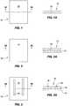
- Fig. 1Ais a diagrammatic cross-section view of Fig. 1 , taken along line 1A-1A in Fig. 1 )
- manufacture of the sensor 10may begin with a substrate 12.
- the substrate 12may be a monolithic, flat, rectangular sheet of material, in an embodiment.
- the materialmay be or may include, for example, nickel and/or titanium ( e.g ., nitinol) or another highly flexible material.
- the substrate 12may be a thin nitinol film.
- a layer of radiopaque material 14may be deposited on the substrate 12.
- the layer of radiopaque material 14may be deposited on either (or, in an embodiment, both) the "top" or "bottom” surface of the substrate 12.
- the radiopaque material 14may be deposited, for example, via magnetron sputtering and stereo lithography.
- the radiopaque material 14may additionally or alternatively be deposited through another appropriate material deposition process, may be printed, or may be applied through a more traditional lamination/epoxy/reflow procedure.
- the radiopaque material 14may be deposited over all or substantially all of one or more sides or surfaces of the substrate 12 (that is, all of the substrate 12 that will be used in the completed sensor 10), in an embodiment.
- the radiopaque material 14may be or may include platinum and/or another material that is highly visible under x-ray.
- the radiopaque materialmay be or may include silver, gold, tantalum, other precious metals, or ceramic.
- the radiopaque materialmay be or may include lead.
- a second layer 16 of magnetically-permeable materialis deposited on the substrate 12 and/or radiopaque material 14.
- the second layer 16may be deposited, for example, via magnetron sputtering and stereo lithography. In embodiments, the second layer 16 may additionally or alternatively be deposited through another appropriate material deposition process, may be printed, or may be applied through a more traditional lamination/epoxy/reflow procedure.
- the second layer 16 of materialincludes a magnetically-permeable material, such as an amorphous magnetic alloy, in an embodiment.
- the magnetically-permeable material 16may include various amounts of cobalt, nickel, and iron, in an embodiment.
- the magnetically-permeable material 16may be a magnetic alloy commercially available under the trade name MetglasTM from MetglasTM, Inc., such as MetglasTM Magnetic Alloy 2714a, or a similar material.
- the magnetically-permeable material 16may include approximately 80% cobalt and approximately 20% nickel, iron, and trace elements, in an embodiment.
- the magnetically-permeable materialmay be or may include another material having high relative magnetic permeability (e.g., about 10), such as mu-metal, in an embodiment.
- the magnetically-permeable material 16may be deposited in a predetermined pattern, in an embodiment.
- the magnetically-permeable material 16may be deposited in one or more strips or lines that extend parallel with the longitudinal axis of the finished sensor (axis A shown in Figs. 5, 5A, 6, and 6A ).
- two such stripsmay be deposited, in an embodiment.
- some other pattern or patternsmay be deposited.
- the second layer 16may be deposited over all or substantially all of one or more sides or surfaces of the radiopaque material 14 and/or substrate 12, in an embodiment.
- a pattern formed by the magnetically-permeable material 16may be pre-formed and then applied to the assembly.
- the stripsmay be fabricated apart from the other layers 12, 14, and then applied to the layers 12, 14.
- the layers 12, 14, 16 of the coremay be extruded.
- the layers of a multi-layer coremay be co-extruded on top of one another.
- the below-described steps of adapting a "flat" sensor core to a tubular sensormay be omitted, as the extrusion steps may result in a tubular core.
- the substrate 12may be a tubular substrate, and the radiopaque material 14 and magnetically-permeable material 16 may be deposited on or applied to the tubular substrate.
- the below-described steps of adapting a "flat" sensor core to a tubular sensormay be omitted.
- Figs. 1-3Aillustrate an embodiment in which a substrate is at the radial center of the assembly, with radiopaque material on the substrate and magnetically-permeable material on the radiopaque material
- this disclosureis not limited to such an arrangement. Rather, in embodiments, the substrate, radiopaque material, and magnetically-permeable material may be arranged in a different order, the layer of radiopaque material may be omitted, and multiple layers of one or more of the material may be provided, for example.
- the layer of magnetically-permeable material 16may be provided as an initial layer (a substrate layer, in effect), and radiopaque material 14 and/or other materials may be deposited or printed on or otherwise applied to the magnetically-permeable material 16 to form the structure of a sensor core.
- flex pads 18may also be placed ( e.g ., deposited) on the substrate 12 and/or magnetically-permeable material 14.
- the flex pads 18may be provided for electrically connecting one or more components of the sensor 10 with separate wiring, in an embodiment.
- Two flex pads 18 1 , 18 2may be provided, in an embodiment-one 18 1 for a first end of a wire defining a coil in the finished sensor 10, and a second 18 2 for the second end of the wire ( see Fig. 6 ).
- a flex pad 18may comprise two or more layers, in an embodiment.
- a first layer of the flex pad 18may be or may include a thin film of deposited silicon oxide insulator or another dielectric, in an embodiment.
- a second layer of the flex pad 18may be or may include gold, or another adequately electrically-conductive material.
- the flex pads 18 being incorporated into the coremay provide an advantage over known sensors by reducing the number of components needed (i.e., eliminating a separate flex pad or electrical connection means), reducing the number of components that may separately fail.
- incorporating the flex pads 18 into the coreprovides the flex pads with structural support.
- one or both of the flex pads 18may extend parallel to the axis A.
- an odd-layer coilmay be enabled without the need to extend the wire of the coil "back" for electrical coupling. That is, at least one of the flex pads 18 may provide electrical coupling for the coil at the distal end of the core 20, and may extend longitudinally to a proximal end of the core 20. As a result, the coil may "begin” at the proximal end of the core 20 and “end” at the distal end, with the end wire of the coil electrically coupled to a flex pad 18 that extends longitudinally over the length of the core 20.
- the manufacturing steps associated with Figs. 1-4Aresult in a "flat" sensor core 20.
- the flat core 20is used in certain embodiments of a sensor 10.
- the "flat" sensor core 20is used to form a tubular sensor core.
- the core 20may have a thickness on the order of thousandths of an inch, for example. In other embodiments, the core 20 may have a thickness that is larger or smaller, depending on the requirements for or desired characteristics of the final device.
- Two ends of the core 22 1 , 22 2are coupled with each other to form such a tubular core, in an embodiment.
- the "flat" core 20may be rolled and two ends 22 1 , 22 2 of the flat core are one of laser welded, brazed, otherwise soldered, or glued to create a hollow cylinder. Accordingly, the ends 22 1 , 22 2 of the flat core 20 are coupled by solder, brazing material, material from laser welding or glue. There can be an identifiable longitudinal seam on the outer surface of the cylinder where the two ends 22 1 , 22 2 of the flat core were joined.
- Figs. 5 and 5A(Fig. 5A is a cross-sectional view of Fig. 5 , taken along line 5A-5A in Fig. 5 ) illustrate the sensor core rolled and bonded to form a hollow cylindrical (i.e., tubular) core 26.
- the radiopaque material 14may be deposited in a pattern such that the tubular core 26 is visible in an x-ray taken from any direction.
- tubular core 26is described here as being formed after the magnetically-permeable material 16 and the radiopaque material 14 have been deposited, in an alternative embodiment, not forming part of the present invention, the magnetically-permeable material 16 and the radiopaque material 14 can be deposited after formation of the tubular core 26.
- Rolling the flat core 20 to form a cylindrical core 26may result in the "top" of the flat assembly being the outer surface 28 of the tubular core 26, and the "bottom” of the flat assembly being the inner surface 30 of the tubular core 26.
- the tubular core 26, or one or more layers 12, 14, 16 of the tubular core 26,may define a longitudinal axis A.
- the substrate 12may be the radially inner-most layer of the core and may define a longitudinal lumen 32.
- the layer of magnetically-permeable material 14may be radially outward of the substrate 12.
- the layer of radiopaque material 16may be radially outward of the layer of magnetically-permeable material 14.
- Fig. 6Ais a diagrammatic cross-sectional view of Fig. 6 , taken along line 6A-6A in Fig. 6
- wireis then wrapped on the hollow cylinder core to form a coil 34.
- the coil 34may include one or more layers of windings, wound at an appropriate pitch and with an appropriate number of layers.
- the coil 34may include windings as disclosed in above-referenced U.S. patent application no. 13/341,396 .
- the wire forming the coil 34may be coupled to the flex pad 18 1 .
- Each flex pad 18may include two or more connection pads 36 and an electrically-conductive trace 38 that electrically couples the connection pads 36 to each other, in an embodiment.
- a first connection pad 36 1 of a flex padmay be electrically coupled with the wire forming the coil 34, and the second connection pad 36 2 of the flex pad may be electrically coupled with a wire 40 that may extend to an exterior system (for example, a magnetic field-based position and navigation system), in an embodiment.
- Wiresmay be electrically coupled with the flex pad 18 1 through soldering or welding, in an embodiment.
- the second flex pad 18 2(not shown in Fig.
- each flex pad 18may simply comprise a single connection pad 36 to which both the wire forming the coil 34 and the wire 40 that may extend to an exterior system are electrically coupled.
- the sensor 10may be incorporated into an elongate medical device, such as a catheter or introducer, another medical device, or another device. As noted above, the sensor may be connected to a position and navigation system, in an embodiment, to navigate the medical device within a patient's body.
- a core including multiple materials and/or multiple layers of materialmay improve on known coil sensors by improving one or more of, for example, shape retention, magnetic permeability, radiopacity, and ease of electrically coupling the coil with separate wiring relative to single-layer/single-material designs.
- the materials comprising the sensormay improve shape retention relative to known sensors, providing a layer of magnetically-permeable material in the core may improve magnetic permeability of a hollow core relative to known hollow-coil sensors, providing a layer of radiopaque material may improve radiopacity relative to known sensors, and providing flex pads on the core may improve ease of electrical coupling.
- joinder referencese.g. , attached, coupled, connected, and the like are to be construed broadly and may include intermediate members between a connection of elements and relative movement between elements. As such, joinder references do not necessarily infer that two elements are directly connected and in fixed relation to each other. It is intended that all matter contained in the above description or shown in the accompanying drawings shall be interpreted as illustrative only and not limiting. Changes in detail or structure may be made within the scope of the invention as defined in the appended claims.
Landscapes
- Engineering & Computer Science (AREA)
- Power Engineering (AREA)
- Health & Medical Sciences (AREA)
- Life Sciences & Earth Sciences (AREA)
- Physics & Mathematics (AREA)
- Microelectronics & Electronic Packaging (AREA)
- General Physics & Mathematics (AREA)
- Heart & Thoracic Surgery (AREA)
- Animal Behavior & Ethology (AREA)
- Biomedical Technology (AREA)
- Biophysics (AREA)
- Medical Informatics (AREA)
- Molecular Biology (AREA)
- Surgery (AREA)
- Pathology (AREA)
- General Health & Medical Sciences (AREA)
- Public Health (AREA)
- Veterinary Medicine (AREA)
- Human Computer Interaction (AREA)
- Measuring Magnetic Variables (AREA)
- Endoscopes (AREA)
- Coils Or Transformers For Communication (AREA)
- Media Introduction/Drainage Providing Device (AREA)
Description
- The instant disclosure relates to sensors, including cores for electromagnetic inductance-based position sensors.
- Magnetic field-based position and navigation systems may be used for, among other things, tracking the location of a medical device to navigate the medical device to a target site in a patient's body. Such position and navigation systems operate on the principles of electromagnetic induction. One magnetic field-based position and navigation system is a system incorporating the MediGuide™ technology commercially available from St. Jude Medical, Inc. of St. Paul, Minnesota. Generally, in magnetic field-based systems, transmitter coils in the system are driven to create a magnetic field. Sensors in the system, which may each include a small inductive coil, are consequently able to detect this magnetic field. These sensors may include coils of wound wire, which in the presence of a magnetic field produce a voltage across the two leads according to the principles of electromagnetic induction.
- A general form for an electromagnetic induction positioning sensor includes wire wrapped on a solid or hollow core. In a "solid core" embodiment, the sensor may have a solid cylindrical core. The solid core may be a solid body of material (i.e., with no lumen through the core). The solid core may be made of mu-metal, in an embodiment. The core of a hollow-core sensor may include a tube with a longitudinal lumen (i.e., a hollow cylinder). The core may include mu-metal or polymer, in an embodiment. Known cores are generally made from a single material-either polymer (e.g., polyimide) or mu-metal.
- The foregoing discussion is intended only to illustrate the present field and should not be taken as a disavowal of claim scope. An apparatus for transmitting electrical signals is known from
US 2014/0209372 A1 . A miniature electromagnetic coil using flexible printed circuitry is known fromUS 2013/0066194 A1 . A guidewire for a medical device is disclosed inUS 2012/0172761 A1 andUS 2013/0296692 A1 . - An exemplary embodiment of a sensor includes a core and a coil. The core includes a rectangular substrate having a top surface, a bottom surface, and four ends, a layer of magnetically-permeable material disposed on at least one of the substrate top surface or the substrate bottom surface, wherein two ends of the substrate are rigidly coupled with each other so as to form a hollow cylinder, by means of one of solder, brazing material, material from laser welding and glue resulting from soldering, brazing, laser welding or gluing said two ends with each other. The hollow cylinder forms a tube such that said top surface is an outer surface of said tube and said bottom surface is an inner surface of said tube. The coil is be wire-wound on the tube.
- An exemplary embodiment of a method of manufacturing a core for a sensor includes providing the rectangular substrate, depositing the layer of magnetically-permeable material on the substrate, and rigidly coupling the two ends of the substrate with each other by one of soldering, brazing 1, laser welding and gluing so as to form the hollow cylinder forming the tube, and wrapping a wire on the tube to form the wire-wound coil.
Fig. 1 is a diagrammatic view of an exemplary embodiment of a portion of a core for a sensor at a stage of manufacture.Fig. 1A is a cross-sectional diagrammatic view of the sensor core portion ofFig. 1 , taken alongline 1A-1A inFig. 1 .Fig. 2 is a diagrammatic view of the sensor core portion ofFig. 1 , at a later stage of manufacture.Fig. 2A is a cross-sectional diagrammatic view of the sensor core portion ofFig. 2 , taken alongline 2A-2A inFig. 2 .Fig. 3 is a cross-sectional diagrammatic view of the sensor core portion ofFigs. 1 and 2 , at a later stage of manufacture.Fig. 3A is a cross-sectional diagrammatic view of the sensor core portion ofFig. 3 , taken alongline 3A-3A inFig. 3 .Fig. 4 is a diagrammatic view of the sensor core portion ofFigs. 1-3 , at a later stage of manufacture.Fig. 4A is a cross-sectional diagrammatic view of the sensor core portion ofFig. 4 , taken alongline 4A-4A inFig. 4 .Fig. 5 is a diagrammatic view of the sensor core portion ofFigs. 1-4 , at a later stage of manufacture.Fig. 5A is a diagrammatic cross-sectional view of the sensor core portion ofFig. 5 , taken alongline 5A-5A inFig. 5 .Fig. 6 is a diagrammatic view of an exemplary embodiment of a sensor including a coil wound on the sensor core portion ofFig. 5 .Fig. 6A is a cross-sectional diagrammatic view of the sensor ofFig. 6 , taken alongline 6A-6A ofFig. 6 .- Various embodiments are described herein to various apparatuses, systems, and/or methods. Numerous specific details are set forth to provide a thorough understanding of the overall structure, function, manufacture, and use of the embodiments as described in the specification and illustrated in the accompanying drawings. It will be understood by those skilled in the art, however, that the embodiments may be practiced without such specific details. In other instances, well-known operations, components, and elements have not been described in detail so as not to obscure the embodiments described in the specification. Those of ordinary skill in the art will understand that the embodiments described and illustrated herein are non-limiting examples, and thus it can be appreciated that the specific structural and functional details disclosed herein may be representative and do not necessarily limit the scope of the embodiments, the scope of which is defined solely by the appended claims.
- Reference throughout the specification to "various embodiments," "some embodiments," "one embodiment," or "an embodiment", or the like, means that a particular feature, structure, or characteristic described in connection with the embodiment is included in at least one embodiment. Thus, appearances of the phrases "in various embodiments," "in some embodiments," "in one embodiment," or "in an embodiment", or the like, in places throughout the specification are not necessarily all referring to the same embodiment. Furthermore, the particular features, structures, or characteristics may be combined in any suitable manner in one or more embodiments. Thus, the particular features, structures, or characteristics illustrated or described in connection with one embodiment may be combined, in whole or in part, with the features structures, or characteristics of one or more other embodiments without limitation given that such combination is not illogical or non-functional.
- The output voltage of an electromagnetic coil sensor (and, thus, the sensitivity of the sensor) is affected by the number of turns of wire in the coil (which may be limited by wire gauge (AWG), core size, and/or other variables), cross-sectional area of the core, and the magnetic permeability of the core. Accordingly, one design feature for a coil sensor that may be altered to increase the sensitivity of the sensor without substantially increasing the size of the sensor is the magnetic permeability of the core. The magnetic permeability of the core may be affected by, among other things, the materials and arrangement of materials that comprise the core.
- Referring to the figures in which like reference numerals refer to the same or similar features in the various views,
Figs. 1-6A are diagrammatic and cross-sectional diagrammatic views of various stages of manufacture of a sensor. It should be understood that the term "sensor" may be used herein to refer to both the finished sensor and to portions of the sensor during manufacture. - A sensor as illustrated and/or described herein may find use, for example only, as a position sensor in a magnetic field-based position and navigation system. An exemplary embodiment of such a system, and the use of a sensor in such a system, is set forth in
U.S. patent application no. 13/341,396, filed December 30, 2011 - It should be understood, however, that this use is exemplary in nature only. The techniques and arrangements illustrated and/or described in this disclosure may find use with other types of sensors or systems, in embodiments.
- Referring to
Figs. 1 and 1A (Fig. 1A is a diagrammatic cross-section view ofFig. 1 , taken alongline 1A-1A inFig. 1 ), manufacture of thesensor 10 may begin with asubstrate 12. Thesubstrate 12 may be a monolithic, flat, rectangular sheet of material, in an embodiment. The material may be or may include, for example, nickel and/or titanium (e.g., nitinol) or another highly flexible material. In an embodiment, thesubstrate 12 may be a thin nitinol film. - As shown in
Figs. 2 and 2A (Fig. 2A is a diagrammatic cross-sectional view ofFig. 2 , taken alongline 2A-2A inFig. 2 ), a layer ofradiopaque material 14 may be deposited on thesubstrate 12. The layer ofradiopaque material 14 may be deposited on either (or, in an embodiment, both) the "top" or "bottom" surface of thesubstrate 12. Theradiopaque material 14 may be deposited, for example, via magnetron sputtering and stereo lithography. In embodiments, theradiopaque material 14 may additionally or alternatively be deposited through another appropriate material deposition process, may be printed, or may be applied through a more traditional lamination/epoxy/reflow procedure. - The
radiopaque material 14 may be deposited over all or substantially all of one or more sides or surfaces of the substrate 12 (that is, all of thesubstrate 12 that will be used in the completed sensor 10), in an embodiment. Theradiopaque material 14 may be or may include platinum and/or another material that is highly visible under x-ray. For example, the radiopaque material may be or may include silver, gold, tantalum, other precious metals, or ceramic. Additionally, in an embodiment in which the teachings of this disclosure are applied in a non-medical application, the radiopaque material may be or may include lead. - Referring to
Figs. 3 and 3A (Fig. 3A is a diagrammatic cross-sectional view ofFig. 3 , taken alongline 3A-3A inFig. 3 ), asecond layer 16 of magnetically-permeable material is deposited on thesubstrate 12 and/orradiopaque material 14. - The
second layer 16 may be deposited, for example, via magnetron sputtering and stereo lithography. In embodiments, thesecond layer 16 may additionally or alternatively be
deposited through another appropriate material deposition process, may be printed, or may be applied through a more traditional lamination/epoxy/reflow procedure. - The
second layer 16 of material includes a magnetically-permeable material, such as an amorphous magnetic alloy, in an embodiment. The magnetically-permeable material 16 may include various amounts of cobalt, nickel, and iron, in an embodiment. For example, the magnetically-permeable material 16 may be a magnetic alloy commercially available under the trade name Metglas™ from Metglas™, Inc., such as Metglas™ Magnetic Alloy 2714a, or a similar material. The magnetically-permeable material 16 may include approximately 80% cobalt and approximately 20% nickel, iron, and trace elements, in an embodiment. Additionally or alternatively, the magnetically-permeable material may be or may include another material having high relative magnetic permeability (e.g., about 10), such as mu-metal, in an embodiment. - The magnetically-
permeable material 16 may be deposited in a predetermined pattern, in an embodiment. For example, the magnetically-permeable material 16 may be deposited in one or more strips or lines that extend parallel with the longitudinal axis of the finished sensor (axis A shown inFigs. 5, 5A, 6, and 6A ). For example, two such strips may be deposited, in an embodiment. Additionally or alternatively, some other pattern or patterns may be deposited. Alternatively, thesecond layer 16 may be deposited over all or substantially all of one or more sides or surfaces of theradiopaque material 14 and/orsubstrate 12, in an embodiment. - In an embodiment not forming part of the claimed invention, a pattern formed by the magnetically-
permeable material 16 may be pre-formed and then applied to the assembly. For example, in the illustrated embodiment in which the magnetically-permeable material 16 is provided in two strips or lines, the strips may be fabricated apart from theother layers layers - In an embodiment, not forming part of the present invention, the
layers substrate 12 may be a tubular substrate, and theradiopaque material 14 and magnetically-permeable material 16 may be deposited on or applied to the tubular substrate. In such an embodiment, the below-described steps of adapting a "flat" sensor core to a tubular sensor may be omitted. - Although
Figs. 1-3A illustrate an embodiment in which a substrate is at the radial center of the assembly, with radiopaque material on the substrate and magnetically-permeable material on the radiopaque material, this disclosure is not limited to such an arrangement. Rather, in embodiments, the substrate, radiopaque material, and magnetically-permeable material may be arranged in a different order, the layer of radiopaque material may be omitted, and multiple layers of one or more of the material may be provided, for example. In another exemplary embodiment, not forming part of the present invention, the layer of magnetically-permeable material 16 may be provided as an initial layer (a substrate layer, in effect), andradiopaque material 14 and/or other materials may be deposited or printed on or otherwise applied to the magnetically-permeable material 16 to form the structure of a sensor core. - As shown in
Figs. 4 and 4A (Fig. 4A is a diagrammatic cross-sectional view ofFig. 4 , taken alongline 4A-4A inFig. 4 ), flex pads 18 (twosuch flex pads Fig. 4 ) may also be placed (e.g., deposited) on thesubstrate 12 and/or magnetically-permeable material 14. Theflex pads 18 may be provided for electrically connecting one or more components of thesensor 10 with separate wiring, in an embodiment. - Two
flex pads one 181 for a first end of a wire defining a coil in thefinished sensor 10, and a second 182 for the second end of the wire (seeFig. 6 ). Aflex pad 18 may comprise two or more layers, in an embodiment. For example, a first layer of theflex pad 18 may be or may include a thin film of deposited silicon oxide insulator or another dielectric, in an embodiment. A second layer of theflex pad 18 may be or may include gold, or another adequately electrically-conductive material. - The
flex pads 18 being incorporated into the core may provide an advantage over known sensors by reducing the number of components needed (i.e., eliminating a separate flex pad or electrical connection means), reducing the number of components that may separately fail. In addition, incorporating theflex pads 18 into the core provides the flex pads with structural support. - Though illustrated as extending orthogonal to the axis A, one or both of the
flex pads 18 may extend parallel to the axis A. In such an embodiment, an odd-layer coil may be enabled without the need to extend the wire of the coil "back" for electrical coupling. That is, at least one of theflex pads 18 may provide electrical coupling for the coil at the distal end of the core 20, and may extend longitudinally to a proximal end of thecore 20. As a result, the coil may "begin" at the proximal end of thecore 20 and "end" at the distal end, with the end wire of the coil electrically coupled to aflex pad 18 that extends longitudinally over the length of thecore 20. - The manufacturing steps associated with
Figs. 1-4A result in a "flat"sensor core 20. Theflat core 20 is used in certain embodiments of asensor 10. In an embodiment of a magnetic position sensor, the "flat"sensor core 20 is used to form a tubular sensor core. In an embodiment, thecore 20 may have a thickness on the order of thousandths of an inch, for example. In other embodiments, thecore 20 may have a thickness that is larger or smaller, depending on the requirements for or desired characteristics of the final device. Two ends of the core 221, 222 are coupled with each other to form such a tubular core, in an embodiment. For example, in an embodiment, the "flat"core 20 may be rolled and two ends 221, 222 of the flat core are one of laser welded, brazed, otherwise soldered, or glued to create a hollow cylinder. Accordingly, the ends 221, 222 of theflat core 20 are coupled by solder, brazing material, material from laser welding or glue. There can be an identifiable longitudinal seam on the outer surface of the cylinder where the two ends 221, 222 of the flat core were joined. Figs. 5 and 5A (Fig. 5A is a cross-sectional view ofFig. 5 , taken alongline 5A-5A inFig. 5 ) illustrate the sensor core rolled and bonded to form a hollow cylindrical (i.e., tubular)core 26. As illustrated inFig. 5A , theradiopaque material 14 may be deposited in a pattern such that thetubular core 26 is visible in an x-ray taken from any direction. Although thetubular core 26 is described here as being formed after the magnetically-permeable material 16 and theradiopaque material 14 have been deposited, in an alternative embodiment, not forming part of the present invention, the magnetically-permeable material 16 and theradiopaque material 14 can be deposited after formation of thetubular core 26.- Rolling the
flat core 20 to form acylindrical core 26 may result in the "top" of the flat assembly being theouter surface 28 of thetubular core 26, and the "bottom" of the flat assembly being theinner surface 30 of thetubular core 26. Thetubular core 26, or one ormore layers tubular core 26, may define a longitudinal axis A. Thesubstrate 12 may be the radially inner-most layer of the core and may define alongitudinal lumen 32. The layer of magnetically-permeable material 14 may be radially outward of thesubstrate 12. The layer ofradiopaque material 16 may be radially outward of the layer of magnetically-permeable material 14. - Referring to
Figs. 6 and 6A (Fig. 6A is a diagrammatic cross-sectional view ofFig. 6 , taken alongline 6A-6A inFig. 6 ), wire is then wrapped on the hollow cylinder core to form acoil 34. Thecoil 34 may include one or more layers of windings, wound at an appropriate pitch and with an appropriate number of layers. For example, thecoil 34 may include windings as disclosed in above-referencedU.S. patent application no. 13/341,396 . - As illustrated in
Fig. 6 , the wire forming thecoil 34 may be coupled to theflex pad 181. Eachflex pad 18 may include two or more connection pads 36 and an electrically-conductive trace 38 that electrically couples the connection pads 36 to each other, in an embodiment. A first connection pad 361 of a flex pad may be electrically coupled with the wire forming thecoil 34, and the second connection pad 362 of the flex pad may be electrically coupled with awire 40 that may extend to an exterior system (for example, a magnetic field-based position and navigation system), in an embodiment. Wires may be electrically coupled with theflex pad 181 through soldering or welding, in an embodiment. The second flex pad 182 (not shown inFig. 6 ) may be similarly electrically coupled with the other end of the wire forming the coil and to the exterior system. In an alternate embodiment, eachflex pad 18 may simply comprise a single connection pad 36 to which both the wire forming thecoil 34 and thewire 40 that may extend to an exterior system are electrically coupled. - The
sensor 10 may be incorporated into an elongate medical device, such as a catheter or introducer, another medical device, or another device. As noted above, the sensor may be connected to a position and navigation system, in an embodiment, to navigate the medical device within a patient's body. - A core including multiple materials and/or multiple layers of material may improve on known coil sensors by improving one or more of, for example, shape retention, magnetic permeability, radiopacity, and ease of electrically coupling the coil with separate wiring relative to single-layer/single-material designs. In particular, the materials comprising the sensor may improve shape retention relative to known sensors, providing a layer of magnetically-permeable material in the core may improve magnetic permeability of a hollow core relative to known hollow-coil sensors, providing a layer of radiopaque material may improve radiopacity relative to known sensors, and providing flex pads on the core may improve ease of electrical coupling.
- Although numerous embodiments of this invention have been described above with a certain degree of particularity, those skilled in the art could make numerous alterations to the disclosed embodiments within the scope of this disclosure. All directional references (e.g., plus, minus, upper, lower, upward, downward, left, right, leftward, rightward, top, bottom, above, below, vertical, horizontal, clockwise, and counterclockwise) are only used for identification purposes to aid the reader's understanding of the present disclosure, and do not create limitations, particularly as to the position, orientation, or use of the any aspect of the disclosure. As used herein, the phrased "configured to," "configured for," and similar phrases indicate that the subject device, apparatus, or system is designed and/or constructed (e.g., through appropriate hardware, software, and/or components) to fulfill one or more specific object purposes, not that the subject device, apparatus, or system is merely capable of performing the object purpose. Joinder references (e.g., attached, coupled, connected, and the like) are to be construed broadly and may include intermediate members between a connection of elements and relative movement between elements. As such, joinder references do not necessarily infer that two elements are directly connected and in fixed relation to each other. It is intended that all matter contained in the above description or shown in the accompanying drawings shall be interpreted as illustrative only and not limiting. Changes in detail or structure may be made within the scope of the invention as defined in the appended claims.
Claims (12)
- A sensor comprising:a core (20, 26) comprising- a rectangular substrate (12) having a top surface, a bottom surface and four ends;- a layer of magnetically-permeable material (16) disposed on at least one of said substrate top surface or said substrate bottom surface;wherein two ends (221, 222) of said substrate (12) are rigidly coupled with each other so as to form a hollow cylinder, by means of one of solder, brazing material, material from laser welding and glue (24) resulting from soldering, brazing, laser welding or gluing said two ends (221, 222) with each other;- the hollow cylinder forming a tube, such that said top surface is an outer surface of said tube and said bottom surface is an inner surface of said tube; anda wire-wound coil (34) wound on said tube.
- The sensor of claim 1, wherein the magnetically-permeable material (16) comprises cobalt and nickel.
- The sensor of claim 1 or 2, wherein the core further comprises a flex pad (181, 182) on at least one of (a) said rectangular substrate (12) or (b) said magnetically-permeable material (16), said flex pad (181, 182) providing an electrical connection for the sensor with an external system.
- The sensor of claim 3, wherein said flex pad (181, 182) comprises:a layer of dielectric material disposed on at least one of (a) said rectangular substrate (12) or (b) said magnetically-permeable material (16); anda layer of electrically-conductive material disposed on said dielectric layer.
- The sensor of any one of claims 1 to 4, wherein said magnetically- permeable material (16) covers at least one of (a) all of said top surface or (b) all of said bottom surface.
- The sensor of any one of claims 1 to 5, wherein the core further comprises a layer (14) of radiopaque material that is highly visible under x-ray and disposed on at least one of (a) said rectangular substrate (12) or (b) said magnetically-permeable material (16).
- The sensor of any one of claims 1 to 6, wherein said substrate (12) comprises nitinol.
- The sensor of any one of claims 1 to7, if dependent on claim 3, wherein the flex pad (181, 182), being electrically conductive, comprises at least two connection pads (36, 361, 362) and an electrically-conductive trace (38) electrically coupling the at least two connection pads, wherein said coil is electrically coupled with one of said connection pads (36, 361, 362).
- A method of manufacturing the sensor according to any one of claims 1 to 8, the method comprising:providing the rectangular substrate (12);depositing the layer of magnetically-permeable material (16) on the substrate (12); andrigidly coupling the two ends (221, 222) of the substrate (12) with each other by one of soldering, brazing, laser welding or gluing so as to form the hollow cylinder forming the tube;wrapping a wire on said tube to form the wire-wound coil (34)
- The method of claim 9, with the sensor being the sensor according to claim 3 or a claim being dependent thereon, further comprising creating the flex pad (181, 182) on at least one of (a) the rectangular substrate (12) or (b) the magnetically-permeable material (16), the flex pad (181, 182) providing an electrical connection for the sensor with an external system.
- The method of claim 10, wherein creating the flex pad (181, 182) comprises:depositing a layer of dielectric material on at least one of (a) the rectangular substrate (12) or (b) the magnetically-permeable material (16); anddepositing a layer of electrically-conductive material on the layer of dielectric material.
- The method of any one of claims 9 to 11, with the sensor being the sensor according to claim 6 or a claim being dependent thereon, further comprising depositing the layer of radiopaque material (14) that is highly visible under x-ray and on at least one of (a) the rectangular substrate (12) or (b) the magnetically-permeable material (16).
Applications Claiming Priority (3)
| Application Number | Priority Date | Filing Date | Title |
|---|---|---|---|
| US201462090768P | 2014-12-11 | 2014-12-11 | |
| US201562128387P | 2015-03-04 | 2015-03-04 | |
| PCT/US2015/065383WO2016094865A1 (en) | 2014-12-11 | 2015-12-11 | Multi-layer sensor core |
Publications (3)
| Publication Number | Publication Date |
|---|---|
| EP3192083A1 EP3192083A1 (en) | 2017-07-19 |
| EP3192083A4 EP3192083A4 (en) | 2018-05-16 |
| EP3192083B1true EP3192083B1 (en) | 2020-08-19 |
Family
ID=56108291
Family Applications (1)
| Application Number | Title | Priority Date | Filing Date |
|---|---|---|---|
| EP15868591.7AActiveEP3192083B1 (en) | 2014-12-11 | 2015-12-11 | Sensor with multi-layer core |
Country Status (3)
| Country | Link |
|---|---|
| US (2) | US10573448B2 (en) |
| EP (1) | EP3192083B1 (en) |
| WO (1) | WO2016094865A1 (en) |
Families Citing this family (6)
| Publication number | Priority date | Publication date | Assignee | Title |
|---|---|---|---|---|
| US10512510B2 (en)* | 2014-12-22 | 2019-12-24 | Intuitive Surgical Operations, Inc. | Flexible electromagnetic sensor |
| US11194071B2 (en)* | 2017-07-19 | 2021-12-07 | Intricon Corporation | Interconnect ring for microminiature electrical coil |
| US10996078B2 (en) | 2017-11-10 | 2021-05-04 | Honeywell International Inc. | C-shaped cylindrical core for linear variable differential transformer (LVDT) probes |
| US10804027B2 (en) | 2018-02-06 | 2020-10-13 | Google Llc | Hollow core electromagnetic coil |
| EP4041076A1 (en)* | 2019-10-11 | 2022-08-17 | Bard Peripheral Vascular, Inc. | Electromagnetic tracking sensor having a flexible core, and methods for making same |
| CN115024821A (en)* | 2022-07-15 | 2022-09-09 | 浙江戴圣思医疗科技有限公司 | Magnetic Positioning Sensors, Invasive Medical Devices and Medical Systems |
Citations (1)
| Publication number | Priority date | Publication date | Assignee | Title |
|---|---|---|---|---|
| US20130066194A1 (en)* | 2011-09-14 | 2013-03-14 | Dan Seter | Method for producing a miniature electromagnetic coil using flexible printed circuitry |
Family Cites Families (17)
| Publication number | Priority date | Publication date | Assignee | Title |
|---|---|---|---|---|
| US5660397A (en) | 1994-09-23 | 1997-08-26 | Holtkamp; William H. | Devices employing a liquid-free medium |
| US20070032746A1 (en)* | 2005-01-10 | 2007-02-08 | Stereotaxis, Inc. | Guide wire with magnetically adjustable bent tip and method for using the same |
| US20070259427A1 (en)* | 2006-03-27 | 2007-11-08 | Storey Daniel M | Modified surfaces for attachment of biological materials |
| NZ546955A (en)* | 2006-05-02 | 2008-09-26 | Auckland Uniservices Ltd | Pick-up apparatus for inductive power transfer systems |
| CN101553890A (en)* | 2006-11-14 | 2009-10-07 | 美商·帕斯脉冲工程有限公司 | Wire-less inductive devices and methods |
| US8747940B2 (en)* | 2007-08-06 | 2014-06-10 | Abbott Cardiovascular Systems Inc. | Manufacturing processes for making medical devices having a coating gradient |
| US20110066029A1 (en) | 2009-09-11 | 2011-03-17 | Medtronic, Inc. | Electromagnetic Medical Device |
| US8764683B2 (en) | 2010-12-29 | 2014-07-01 | Mediguide Ltd. | Medical device guidewire with a position sensor |
| US9427172B2 (en) | 2011-12-30 | 2016-08-30 | Mediguide Ltd. | Roll detection and six degrees of freedom sensor assembly |
| US9364640B2 (en)* | 2012-05-07 | 2016-06-14 | St. Jude Medical Atrial Fibrillation Division, Inc. | Medical device guidewire with helical cutout and coating |
| US9101046B2 (en) | 2013-01-29 | 2015-08-04 | Mediguide Ltd. | Shielded twisted pair of conductors using conductive ink |
| US10115661B2 (en) | 2013-02-08 | 2018-10-30 | Qualcomm Incorporated | Substrate-less discrete coupled inductor structure |
| US9111557B2 (en)* | 2013-10-04 | 2015-08-18 | Seagate Technology Llc | Electrically insulating magnetic material for a read head |
| WO2015061034A1 (en)* | 2013-10-24 | 2015-04-30 | St. Jude Medical, Cardiology Division, Inc. | Flexible catheter shaft and method of manufacture |
| HUE044648T2 (en)* | 2014-05-21 | 2019-11-28 | Dentsply Ih Ab | Reinforced urinary catheter |
| US10602983B2 (en)* | 2015-05-08 | 2020-03-31 | St. Jude Medical International Holding S.À R.L. | Integrated sensors for medical devices and method of making integrated sensors for medical devices |
| US11040173B2 (en)* | 2016-11-21 | 2021-06-22 | St. Jude Medical International Holding S.À R.L. | Medical device sensor |
- 2015
- 2015-12-11EPEP15868591.7Apatent/EP3192083B1/enactiveActive
- 2015-12-11WOPCT/US2015/065383patent/WO2016094865A1/enactiveApplication Filing
- 2015-12-11USUS15/535,319patent/US10573448B2/enactiveActive
- 2020
- 2020-01-16USUS16/745,081patent/US11017929B2/enactiveActive
Patent Citations (1)
| Publication number | Priority date | Publication date | Assignee | Title |
|---|---|---|---|---|
| US20130066194A1 (en)* | 2011-09-14 | 2013-03-14 | Dan Seter | Method for producing a miniature electromagnetic coil using flexible printed circuitry |
Also Published As
| Publication number | Publication date |
|---|---|
| EP3192083A1 (en) | 2017-07-19 |
| US10573448B2 (en) | 2020-02-25 |
| US20200227192A1 (en) | 2020-07-16 |
| EP3192083A4 (en) | 2018-05-16 |
| US11017929B2 (en) | 2021-05-25 |
| US20170358388A1 (en) | 2017-12-14 |
| WO2016094865A1 (en) | 2016-06-16 |
Similar Documents
| Publication | Publication Date | Title |
|---|---|---|
| US11017929B2 (en) | Multi-layer sensor core | |
| EP3082588B1 (en) | Elongate medical devices incorporating a flexible substrate, a sensor, and electrically-conductive traces | |
| CN108420403B (en) | Multi-axial position sensor printed on a folded flexible circuit board | |
| US20190254560A1 (en) | Method for producing a miniature electromagnetic coil using flexible printed circuitry | |
| US8761900B2 (en) | MRI compatible electrode circuit | |
| EP1806756A2 (en) | Miniature coils on core with printed circuit | |
| US11779239B2 (en) | Core designs for miniature inductive coil sensors | |
| WO2012150974A2 (en) | Sensor assembly tethered within catheter wall | |
| US20220032011A1 (en) | Microminiature EM Coil Sensor Pull Ring For Catheter | |
| US11538624B2 (en) | Wire wound inductor and manufacturing method thereof | |
| US8855788B2 (en) | MRI compatible electrode circuit | |
| CN114554949B (en) | Electromagnetic tracking sensor with flexible core and method of manufacturing the same | |
| JP2017506090A (en) | Method and apparatus for assembling an electrically stable connector | |
| US8761899B2 (en) | MRI compatible conductive wires | |
| US11194071B2 (en) | Interconnect ring for microminiature electrical coil | |
| US8831743B2 (en) | MRI compatible electrode circuit | |
| RU2838162C1 (en) | Inductive component and inductance value adjustment method | |
| EP4483799A1 (en) | A system and method of sensing catheter's location and force | |
| US20220336150A1 (en) | Inductive component and method for adjusting an inductance value | |
| CN117497280A (en) | Induction coil assembly and magnetic field sensor |
Legal Events
| Date | Code | Title | Description |
|---|---|---|---|
| STAA | Information on the status of an ep patent application or granted ep patent | Free format text:STATUS: THE INTERNATIONAL PUBLICATION HAS BEEN MADE | |
| PUAI | Public reference made under article 153(3) epc to a published international application that has entered the european phase | Free format text:ORIGINAL CODE: 0009012 | |
| STAA | Information on the status of an ep patent application or granted ep patent | Free format text:STATUS: REQUEST FOR EXAMINATION WAS MADE | |
| 17P | Request for examination filed | Effective date:20170410 | |
| AK | Designated contracting states | Kind code of ref document:A1 Designated state(s):AL AT BE BG CH CY CZ DE DK EE ES FI FR GB GR HR HU IE IS IT LI LT LU LV MC MK MT NL NO PL PT RO RS SE SI SK SM TR | |
| AX | Request for extension of the european patent | Extension state:BA ME | |
| DAV | Request for validation of the european patent (deleted) | ||
| DAX | Request for extension of the european patent (deleted) | ||
| A4 | Supplementary search report drawn up and despatched | Effective date:20180412 | |
| RIC1 | Information provided on ipc code assigned before grant | Ipc:H01F 3/00 20060101AFI20180406BHEP Ipc:H01F 10/13 20060101ALI20180406BHEP Ipc:H01F 3/04 20060101ALI20180406BHEP Ipc:H01F 17/00 20060101ALI20180406BHEP Ipc:H01F 5/00 20060101ALI20180406BHEP Ipc:A61B 5/06 20060101ALI20180406BHEP | |
| RAP1 | Party data changed (applicant data changed or rights of an application transferred) | Owner name:ST. JUDE MEDICAL INTERNATIONAL HOLDING S.A R.L. | |
| STAA | Information on the status of an ep patent application or granted ep patent | Free format text:STATUS: EXAMINATION IS IN PROGRESS | |
| 17Q | First examination report despatched | Effective date:20190214 | |
| GRAP | Despatch of communication of intention to grant a patent | Free format text:ORIGINAL CODE: EPIDOSNIGR1 | |
| STAA | Information on the status of an ep patent application or granted ep patent | Free format text:STATUS: GRANT OF PATENT IS INTENDED | |
| RIC1 | Information provided on ipc code assigned before grant | Ipc:H01F 10/13 20060101ALI20200305BHEP Ipc:A61B 5/06 20060101ALI20200305BHEP Ipc:G01B 7/00 20060101ALI20200305BHEP Ipc:H01F 3/00 20060101ALI20200305BHEP Ipc:H01F 5/00 20060101ALI20200305BHEP Ipc:H01F 17/00 20060101ALI20200305BHEP Ipc:H01F 3/04 20060101AFI20200305BHEP | |
| INTG | Intention to grant announced | Effective date:20200326 | |
| GRAS | Grant fee paid | Free format text:ORIGINAL CODE: EPIDOSNIGR3 | |
| GRAA | (expected) grant | Free format text:ORIGINAL CODE: 0009210 | |
| STAA | Information on the status of an ep patent application or granted ep patent | Free format text:STATUS: THE PATENT HAS BEEN GRANTED | |
| AK | Designated contracting states | Kind code of ref document:B1 Designated state(s):AL AT BE BG CH CY CZ DE DK EE ES FI FR GB GR HR HU IE IS IT LI LT LU LV MC MK MT NL NO PL PT RO RS SE SI SK SM TR | |
| REG | Reference to a national code | Ref country code:CH Ref legal event code:EP | |
| REG | Reference to a national code | Ref country code:DE Ref legal event code:R096 Ref document number:602015057870 Country of ref document:DE | |
| REG | Reference to a national code | Ref country code:AT Ref legal event code:REF Ref document number:1304877 Country of ref document:AT Kind code of ref document:T Effective date:20200915 | |
| REG | Reference to a national code | Ref country code:IE Ref legal event code:FG4D | |
| REG | Reference to a national code | Ref country code:LT Ref legal event code:MG4D | |
| REG | Reference to a national code | Ref country code:NL Ref legal event code:MP Effective date:20200819 | |
| PG25 | Lapsed in a contracting state [announced via postgrant information from national office to epo] | Ref country code:BG Free format text:LAPSE BECAUSE OF FAILURE TO SUBMIT A TRANSLATION OF THE DESCRIPTION OR TO PAY THE FEE WITHIN THE PRESCRIBED TIME-LIMIT Effective date:20201119 Ref country code:GR Free format text:LAPSE BECAUSE OF FAILURE TO SUBMIT A TRANSLATION OF THE DESCRIPTION OR TO PAY THE FEE WITHIN THE PRESCRIBED TIME-LIMIT Effective date:20201120 Ref country code:LT Free format text:LAPSE BECAUSE OF FAILURE TO SUBMIT A TRANSLATION OF THE DESCRIPTION OR TO PAY THE FEE WITHIN THE PRESCRIBED TIME-LIMIT Effective date:20200819 Ref country code:FI Free format text:LAPSE BECAUSE OF FAILURE TO SUBMIT A TRANSLATION OF THE DESCRIPTION OR TO PAY THE FEE WITHIN THE PRESCRIBED TIME-LIMIT Effective date:20200819 Ref country code:PT Free format text:LAPSE BECAUSE OF FAILURE TO SUBMIT A TRANSLATION OF THE DESCRIPTION OR TO PAY THE FEE WITHIN THE PRESCRIBED TIME-LIMIT Effective date:20201221 Ref country code:HR Free format text:LAPSE BECAUSE OF FAILURE TO SUBMIT A TRANSLATION OF THE DESCRIPTION OR TO PAY THE FEE WITHIN THE PRESCRIBED TIME-LIMIT Effective date:20200819 Ref country code:SE Free format text:LAPSE BECAUSE OF FAILURE TO SUBMIT A TRANSLATION OF THE DESCRIPTION OR TO PAY THE FEE WITHIN THE PRESCRIBED TIME-LIMIT Effective date:20200819 Ref country code:NO Free format text:LAPSE BECAUSE OF FAILURE TO SUBMIT A TRANSLATION OF THE DESCRIPTION OR TO PAY THE FEE WITHIN THE PRESCRIBED TIME-LIMIT Effective date:20201119 | |
| REG | Reference to a national code | Ref country code:AT Ref legal event code:MK05 Ref document number:1304877 Country of ref document:AT Kind code of ref document:T Effective date:20200819 | |
| PG25 | Lapsed in a contracting state [announced via postgrant information from national office to epo] | Ref country code:IS Free format text:LAPSE BECAUSE OF FAILURE TO SUBMIT A TRANSLATION OF THE DESCRIPTION OR TO PAY THE FEE WITHIN THE PRESCRIBED TIME-LIMIT Effective date:20201219 Ref country code:RS Free format text:LAPSE BECAUSE OF FAILURE TO SUBMIT A TRANSLATION OF THE DESCRIPTION OR TO PAY THE FEE WITHIN THE PRESCRIBED TIME-LIMIT Effective date:20200819 Ref country code:PL Free format text:LAPSE BECAUSE OF FAILURE TO SUBMIT A TRANSLATION OF THE DESCRIPTION OR TO PAY THE FEE WITHIN THE PRESCRIBED TIME-LIMIT Effective date:20200819 Ref country code:NL Free format text:LAPSE BECAUSE OF FAILURE TO SUBMIT A TRANSLATION OF THE DESCRIPTION OR TO PAY THE FEE WITHIN THE PRESCRIBED TIME-LIMIT Effective date:20200819 Ref country code:LV Free format text:LAPSE BECAUSE OF FAILURE TO SUBMIT A TRANSLATION OF THE DESCRIPTION OR TO PAY THE FEE WITHIN THE PRESCRIBED TIME-LIMIT Effective date:20200819 | |
| PG25 | Lapsed in a contracting state [announced via postgrant information from national office to epo] | Ref country code:SM Free format text:LAPSE BECAUSE OF FAILURE TO SUBMIT A TRANSLATION OF THE DESCRIPTION OR TO PAY THE FEE WITHIN THE PRESCRIBED TIME-LIMIT Effective date:20200819 Ref country code:RO Free format text:LAPSE BECAUSE OF FAILURE TO SUBMIT A TRANSLATION OF THE DESCRIPTION OR TO PAY THE FEE WITHIN THE PRESCRIBED TIME-LIMIT Effective date:20200819 Ref country code:EE Free format text:LAPSE BECAUSE OF FAILURE TO SUBMIT A TRANSLATION OF THE DESCRIPTION OR TO PAY THE FEE WITHIN THE PRESCRIBED TIME-LIMIT Effective date:20200819 Ref country code:CZ Free format text:LAPSE BECAUSE OF FAILURE TO SUBMIT A TRANSLATION OF THE DESCRIPTION OR TO PAY THE FEE WITHIN THE PRESCRIBED TIME-LIMIT Effective date:20200819 Ref country code:DK Free format text:LAPSE BECAUSE OF FAILURE TO SUBMIT A TRANSLATION OF THE DESCRIPTION OR TO PAY THE FEE WITHIN THE PRESCRIBED TIME-LIMIT Effective date:20200819 | |
| REG | Reference to a national code | Ref country code:DE Ref legal event code:R097 Ref document number:602015057870 Country of ref document:DE | |
| PG25 | Lapsed in a contracting state [announced via postgrant information from national office to epo] | Ref country code:AT Free format text:LAPSE BECAUSE OF FAILURE TO SUBMIT A TRANSLATION OF THE DESCRIPTION OR TO PAY THE FEE WITHIN THE PRESCRIBED TIME-LIMIT Effective date:20200819 Ref country code:AL Free format text:LAPSE BECAUSE OF FAILURE TO SUBMIT A TRANSLATION OF THE DESCRIPTION OR TO PAY THE FEE WITHIN THE PRESCRIBED TIME-LIMIT Effective date:20200819 Ref country code:ES Free format text:LAPSE BECAUSE OF FAILURE TO SUBMIT A TRANSLATION OF THE DESCRIPTION OR TO PAY THE FEE WITHIN THE PRESCRIBED TIME-LIMIT Effective date:20200819 | |
| PLBE | No opposition filed within time limit | Free format text:ORIGINAL CODE: 0009261 | |
| STAA | Information on the status of an ep patent application or granted ep patent | Free format text:STATUS: NO OPPOSITION FILED WITHIN TIME LIMIT | |
| PG25 | Lapsed in a contracting state [announced via postgrant information from national office to epo] | Ref country code:SK Free format text:LAPSE BECAUSE OF FAILURE TO SUBMIT A TRANSLATION OF THE DESCRIPTION OR TO PAY THE FEE WITHIN THE PRESCRIBED TIME-LIMIT Effective date:20200819 | |
| 26N | No opposition filed | Effective date:20210520 | |
| REG | Reference to a national code | Ref country code:CH Ref legal event code:PL | |
| PG25 | Lapsed in a contracting state [announced via postgrant information from national office to epo] | Ref country code:SI Free format text:LAPSE BECAUSE OF FAILURE TO SUBMIT A TRANSLATION OF THE DESCRIPTION OR TO PAY THE FEE WITHIN THE PRESCRIBED TIME-LIMIT Effective date:20200819 Ref country code:MC Free format text:LAPSE BECAUSE OF FAILURE TO SUBMIT A TRANSLATION OF THE DESCRIPTION OR TO PAY THE FEE WITHIN THE PRESCRIBED TIME-LIMIT Effective date:20200819 | |
| REG | Reference to a national code | Ref country code:BE Ref legal event code:MM Effective date:20201231 | |
| PG25 | Lapsed in a contracting state [announced via postgrant information from national office to epo] | Ref country code:IE Free format text:LAPSE BECAUSE OF NON-PAYMENT OF DUE FEES Effective date:20201211 Ref country code:LU Free format text:LAPSE BECAUSE OF NON-PAYMENT OF DUE FEES Effective date:20201211 | |
| PG25 | Lapsed in a contracting state [announced via postgrant information from national office to epo] | Ref country code:CH Free format text:LAPSE BECAUSE OF NON-PAYMENT OF DUE FEES Effective date:20201231 Ref country code:LI Free format text:LAPSE BECAUSE OF NON-PAYMENT OF DUE FEES Effective date:20201231 | |
| PG25 | Lapsed in a contracting state [announced via postgrant information from national office to epo] | Ref country code:TR Free format text:LAPSE BECAUSE OF FAILURE TO SUBMIT A TRANSLATION OF THE DESCRIPTION OR TO PAY THE FEE WITHIN THE PRESCRIBED TIME-LIMIT Effective date:20200819 Ref country code:MT Free format text:LAPSE BECAUSE OF FAILURE TO SUBMIT A TRANSLATION OF THE DESCRIPTION OR TO PAY THE FEE WITHIN THE PRESCRIBED TIME-LIMIT Effective date:20200819 Ref country code:CY Free format text:LAPSE BECAUSE OF FAILURE TO SUBMIT A TRANSLATION OF THE DESCRIPTION OR TO PAY THE FEE WITHIN THE PRESCRIBED TIME-LIMIT Effective date:20200819 | |
| PG25 | Lapsed in a contracting state [announced via postgrant information from national office to epo] | Ref country code:MK Free format text:LAPSE BECAUSE OF FAILURE TO SUBMIT A TRANSLATION OF THE DESCRIPTION OR TO PAY THE FEE WITHIN THE PRESCRIBED TIME-LIMIT Effective date:20200819 | |
| PG25 | Lapsed in a contracting state [announced via postgrant information from national office to epo] | Ref country code:BE Free format text:LAPSE BECAUSE OF NON-PAYMENT OF DUE FEES Effective date:20201231 | |
| P01 | Opt-out of the competence of the unified patent court (upc) registered | Effective date:20230602 | |
| REG | Reference to a national code | Ref country code:DE Ref legal event code:R082 Ref document number:602015057870 Country of ref document:DE Representative=s name:ALPSPITZ IP ALLGAYER UND PARTNER PATENTANWAELT, DE | |
| PGFP | Annual fee paid to national office [announced via postgrant information from national office to epo] | Ref country code:DE Payment date:20241111 Year of fee payment:10 | |
| PGFP | Annual fee paid to national office [announced via postgrant information from national office to epo] | Ref country code:GB Payment date:20241114 Year of fee payment:10 | |
| PGFP | Annual fee paid to national office [announced via postgrant information from national office to epo] | Ref country code:FR Payment date:20241111 Year of fee payment:10 | |
| PGFP | Annual fee paid to national office [announced via postgrant information from national office to epo] | Ref country code:IT Payment date:20241212 Year of fee payment:10 |