EP3191969B1 - Serial sideband signaling link - Google Patents
Serial sideband signaling linkDownload PDFInfo
- Publication number
- EP3191969B1 EP3191969B1EP14901804.6AEP14901804AEP3191969B1EP 3191969 B1EP3191969 B1EP 3191969B1EP 14901804 AEP14901804 AEP 14901804AEP 3191969 B1EP3191969 B1EP 3191969B1
- Authority
- EP
- European Patent Office
- Prior art keywords
- sideband
- signaling
- serial
- link
- sideband link
- Prior art date
- Legal status (The legal status is an assumption and is not a legal conclusion. Google has not performed a legal analysis and makes no representation as to the accuracy of the status listed.)
- Active
Links
Images


Classifications
- G—PHYSICS
- G06—COMPUTING OR CALCULATING; COUNTING
- G06F—ELECTRIC DIGITAL DATA PROCESSING
- G06F13/00—Interconnection of, or transfer of information or other signals between, memories, input/output devices or central processing units
- G06F13/38—Information transfer, e.g. on bus
- G06F13/42—Bus transfer protocol, e.g. handshake; Synchronisation
- G06F13/4282—Bus transfer protocol, e.g. handshake; Synchronisation on a serial bus, e.g. I2C bus, SPI bus
- G06F13/4286—Bus transfer protocol, e.g. handshake; Synchronisation on a serial bus, e.g. I2C bus, SPI bus using a handshaking protocol, e.g. RS232C link
- G—PHYSICS
- G06—COMPUTING OR CALCULATING; COUNTING
- G06F—ELECTRIC DIGITAL DATA PROCESSING
- G06F13/00—Interconnection of, or transfer of information or other signals between, memories, input/output devices or central processing units
- G06F13/38—Information transfer, e.g. on bus
- G06F13/382—Information transfer, e.g. on bus using universal interface adapter
- G06F13/385—Information transfer, e.g. on bus using universal interface adapter for adaptation of a particular data processing system to different peripheral devices
- G—PHYSICS
- G06—COMPUTING OR CALCULATING; COUNTING
- G06F—ELECTRIC DIGITAL DATA PROCESSING
- G06F13/00—Interconnection of, or transfer of information or other signals between, memories, input/output devices or central processing units
- G06F13/38—Information transfer, e.g. on bus
- G06F13/40—Bus structure
- G06F13/4004—Coupling between buses
- G06F13/4027—Coupling between buses using bus bridges
- G—PHYSICS
- G06—COMPUTING OR CALCULATING; COUNTING
- G06F—ELECTRIC DIGITAL DATA PROCESSING
- G06F13/00—Interconnection of, or transfer of information or other signals between, memories, input/output devices or central processing units
- G06F13/38—Information transfer, e.g. on bus
- G06F13/42—Bus transfer protocol, e.g. handshake; Synchronisation
- G—PHYSICS
- G06—COMPUTING OR CALCULATING; COUNTING
- G06F—ELECTRIC DIGITAL DATA PROCESSING
- G06F2213/00—Indexing scheme relating to interconnection of, or transfer of information or other signals between, memories, input/output devices or central processing units
- G06F2213/0042—Universal serial bus [USB]
- G—PHYSICS
- G06—COMPUTING OR CALCULATING; COUNTING
- G06F—ELECTRIC DIGITAL DATA PROCESSING
- G06F2213/00—Indexing scheme relating to interconnection of, or transfer of information or other signals between, memories, input/output devices or central processing units
- G06F2213/40—Bus coupling
- G06F2213/4002—Universal serial bus hub with a single upstream port
Definitions
- This disclosurerelates generally to sideband signaling. Specifically, this disclosure relates to a serial sideband signaling link.
- signaling link technologiesmay have a main signaling link and be associated with sideband signals that are not configured to propagate over the main signaling link.
- Sideband link input/output (I/O) technologiesprovide a way for a sideband signal to be provided from one component within a computing device to another component without being propagated on the main signaling link.
- PCIePeripheral Component Interconnect Express
- sideband signalsmay be propagated through a number of different sideband I/OP technologies such as a Card Electromechanical (CEM) sideband link, a mini CEM, a System Management Bus (SMBus), and the like.
- CEMCard Electromechanical
- SMBSystem Management Bus
- motherboard manufacturersmay desire to modify existing sideband technologies by using glue logic.
- Glue logicis one or more custom logic modifications made to a sideband signaling link.
- glue logicis difficult to implement with existing sideband I/O technologies as design and operation of these technologies may be sophisticated in comparison to the glue logic.
- the techniques described hereininclude a serial sideband link.
- the serial sideband linkincludes a first serial sideband link module configured to propagate signals in one direction, and a second serial sideband link module configured to propagate signals in another direction.
- the serial sideband linkmay be used to consolidate other sideband link I/O technologies, such as CEM, Mini CEM, and the like, into a single serial sideband link, thereby potentially reducing pin count on any given connected components.
- the serial sideband linkmay also enable a scalable number of sideband signals to be added without adding pin count.
- Fig. 1illustrates a block diagram of serial sideband links between an upstream port and a downstream port.
- An upstream port 102may be communicatively coupled to a downstream port 104 via a main signaling link 106.
- Sideband signalsmay be propagated over a serial sideband signaling link 108.
- sideband signalsmay be propagated in one direction by a first serial sideband link module 110, and in an opposite direction by a second serial sideband link module 112.
- the main signaling link 106may be a PCIe fabric, and sideband signals are propagated on the serial sideband signaling link 108.
- the downstream port 104is a controller, such as a system on chip (SoC)
- the upstream port 102may be a device, such as an expansion card communicatively coupled to a SoC.
- SoCsystem on chip
- the first serial sideband link module 110is to propagate signals from the upstream port 102 to the downstream port 104 on a first signaling lane 114.
- the second serial sideband link module 112is to propagate signals from the downstream port 104 to the upstream port 102 via a second signaling lane 116.
- Fig 2illustrates a number of scenarios where a serial sideband link consolidates sideband signals.
- a SoC 204is communicatively coupled to a device 206 through the serial sideband link 108.
- the device 206may be connected to one or more sideband link I/O technologies via a connector 208.
- the connector 208may be a connecter associated with sideband link technologies such as CEM, mini CEM, SMBus, and the like.
- the serial sideband link 108is backwards compatible to other legacy sideband technologies, as well as any further sideband technologies.
- the serial sideband link 108may convert voltages to a 1.8 volt (V) domain that is compatible with the SoC 204 at glue logic 210.
- glue logic 210may be disposed on either side of the connector 208, and the serial sideband link 108 may be used on either side of the glue logic 210.
- glue logicmay not be used to connect the connector to the serial sideband link 108, as indicated at 214.
- the serial sideband link 108may directly interface with the connector 208.
- the serial sideband link 108may communicatively couple the SoC 204 to the device 206 via integrated components of the serial sideband link 108 within the SoC 204 and the device 206, as indicated at 216.
- Fig. 3is a diagram illustrating timing of an asynchronous handshake.
- the serial sideband link 108may be in an idle state, and either side can be clock and/or power gated.
- An asynchronous handshake performed on either side of the linkmay be used to wake up a remote side. If either side is clock and/or power gated, this asynchronous handshake should be used to start the phase locked loops (PLLs) and establish stable power and clocks in order to correctly receive a serial bit stream on the serial sideband link 108.
- PLLsphase locked loops
- the side that initiates the asynchronous handshakemay be referred to herein as an initiator, indicated at 302, and the side that receives the asynchronous handshake may be referred to herein as a responder, indicated at 304.
- the initiator 302 and the responder 304may be either upstream ports, or downstream ports, such as the ports 102 and 104 discussed above in regard to Fig. 1 .
- the initiator 302initiates the asynchronous handshake by asserting a sideband signal of a predetermined high voltage.
- the responder 304acknowledges the start of the asynchronous handshake by asserting a sideband signal of the predetermined high voltage.
- the initiator 302keeps the signal asserted for a first time period, indicated by T MIN _ ACTIVE in Fig. 3 .
- Both the initiator 302 and the responder 304are configured to de-assert their sideband signals any time after T MIN _ ACTIVE . It is assumed that either side de-asserts their respective predetermined high voltage only when all required clocks are active and stable.
- a byte valueis transmitted using pulse width modulation (PWM) encoding to help the responder 304 recover a clock, as indicated at 306.
- PWMpulse width modulation
- the byte valueis an 8 bit value, wherein the first seven bits are of a value of 1 and the last bit is of a value of 0. This simple value may enable relatively quick clock recovery.
- a profile negotiation, and/or a serial sideband signal packetmay follow, as indicated at 308. If the serial sideband link is idle for a second time period, indicated by T MAX_IDLE in Fig. 3 and a sideband packet has to be transmitted, then the asynchronous handshake is repeated.
- both sidesmay initiate a handshake simultaneously.
- an upstream portsuch as the upstream port 102 of Fig. 1
- a downstream portsuch as the downstream port 104 of Fig. 1
- Both ports 102 and 104keep the signal asserted for T MIN _ ACTIVE .
- Both the downstream port 104 and the upstream port 102are configured to de-assert their sideband signals any time after T MIN _ ACTIVE . It is assumed that either side de-asserts only when all the clocks of the respective port are active and stable in either separate reference clock or common clock configurations.
- a byte valueis transmitted using PWM encoding to help either side recover a clock, as indicated at 310.
- the byte valueis an 8 bit value, wherein the first seven bits are of a value of 1 and the last bit is of a value of 0.
- a profile negotiation, and/or a serial sideband signal packetmay follow, as indicated at 312. If the serial sideband link is idle for a second time period, indicated by T MAX_IDLE in Fig. 3 and a sideband packet is to be transmitted, then the asynchronous handshake is repeated.
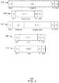
- Fig. 4is a diagram illustrating various packet formats of the serial sideband link.
- the various packet formatsinclude a profile negotiation 402, sideband signals for a fixed profile 404, sideband signals for a dynamic profile 406, an acknowledgement (ACK) packet 408, a non-acknowledgement (NAK) packet 410, and the like.
- the packet format fieldsmay be indicated in Table 1 below: Table 1 Field Name Description SOP Start of Packet (2'b10) PROFILE ID 16 bit profile register indication support for or the selected profile P Odd parity bit for the entire packet excluding SOP and EOP EOP End of Packet (2'b01)
- the asynchronous handshakemay be used during power on reset, hot plug events, and the like.
- a hot plug eventmay also include a hot unplug event.
- Hot plug and hot unplug eventsinclude adding or removing components, such as an upstream port 102 of an expansion card, from connection with a downstream port 104 without prior indication.
- an asynchronous handshakemay be performed, and a profile negotiation may follow, as discussed in more detail below. If either side does not support certain bits in a given profile, they are to be ignored by the receiving side.
- the serial sideband link 108may be configured to perform a profile negotiation every time there is a hot plug event, state changes, or any combination thereof. In these circumstances, a profile negotiation is performed following the very first asynchronous handshake after these events.
- Fig. 5is a diagram illustrating a profile negotiation packet.
- Each end of the serial sideband linksuch as the serial sideband link 108 of Fig. 1 , is configured to maintain a 16 bit register indicating support for various profiles that may be supported by each end. Profiles are used to enable operation across various use cases such as different form factors, I/O technologies, SoC designs, and the like. Each profile defines a certain set of sideband signals. The one or more profiles to be used during serial sideband link operation may be negotiated only once during initialization out of reset. The profile negotiation is discussed below in regard to Fig. 7A and Fig. 7B .
- the profile negotiation packetmay also include an "L" value indicating whether a port is transmitting a last profile of a plurality of profiles supported, indicated at 502.
- An example of the fields in the registeris indicated in Table 2 below: Table2 Profile ID Description S0-P0 CEM S0-P1 Mini CEM S0-P2 M.2 S0-P3 SFF S0-P4 Retimer S0-P5 to S0-P15 Reserved S1-Px to S7-Px
- existing sideband link I/O technologiesmay be identified in the profile register of the serial sideband link 108.
- the identificationis performed by logic of the one or more of the serial sideband link modules 110 and 112, discussed above with regard to Fig. 1 .
- the serial sideband link techniques discussed hereinmay be scalable to add additional sideband link I/O technologies in profile ID fields 6-15.
- Fig. 6is a diagram illustrating an example packet format for a CEM profile.
- existing sideband link I/O technologiesmay be identified by the serial sideband link 108.
- the serial sideband link 108 of Fig. 1may identify CEM as an existing sideband link technology communicatively coupled to the serial sideband link 108.
- the CEMmay use Optimized Buffer Flush/Fill (OBFF) toggle mechanisms of a single pin.
- OBFFOptimized Buffer Flush/Fill
- the serial sideband link 108may, via a serial sideband link module 110, 112, encode any signals from the CEM such that CEM information is sent as a 2 bit code across the serial sideband link 108.
- a packet format 602 of the serial sideband link 108is illustrated in Fig. 6 .
- the CEM profile detailsmay be illustrated by Table 3 below: Table 3 Serial Bits D2U_P0 U2D_P0 Description b0 OBFF bit 1 - 4 OBFF messages encoded in a binary code b1 OBFF bit 0 - b2 CLKREQ# CLKREQ# Clock request b3 WAKE# Wake signal b4 PERST# - Fundamental Reset
- OBFF messageshave been encoded as a 2 bit code instead of relying on rising and falling edges. Different values in the profile bits may lead to different number of bits causing different sideband signals to be propagated on the serial sideband link 108.
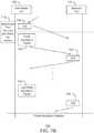
- Fig. 7A and Fig. 7Bare diagrams illustrating profile negotiation on the serial sideband link.
- a profile negotiationmay occur.
- the profile negotiationdetermines the one or more profiles available at each port, such as the upstream port 102 and the downstream port 104 of Fig. 1 .
- the profile determinationdefines the sideband signals in the packets that are exchanged.
- the profile negotiationtakes place immediately following a byte value, such as the byte value 306, propagated as discussed above in regard to Fig. 3 .
- a downstream portsuch as the downstream port 104 of Fig. 1 , sends a profile negotiation packet with a value of 1 set in all the profiles that it supports, as indicated at 702.
- the packetis received at an upstream port, such as the upstream port 102 of Fig. 1 .
- the upstream port 102transmits an acknowledgement (ACK) packet, as indicated at 704, upon successfully receiving a profile negotiation packet.
- ACKacknowledgement
- the downstream port 104may be configured to refrain from transmitting another profile negotiation packet until it receives an ACK packet for the last profile negotiation packet it has transmitted at 702. If the downstream port 104 receives a non-acknowledgement (NAK) packet, or after two milliseconds, the same profile negotiation packet will be retransmitted.
- NAKnon-acknowledgement
- the downstream port 104is configured to transmit a value of 0 in an "L" field, such the L field indicated in Fig. 5 .
- the downstream port 104is configured to transmit the value of 1 in the L field if there are more sets to be transmitted.
- the downstream port 104sets a value of 1 in field L field it is transmitting a final profile of a plurality of profiles supported by the downstream port 104, as indicated at 706.
- the upstream portmay be configured to transit an ACK packet as indicated at 708.
- the upstream port 102may be further configured to transmit a profile negotiation packet, as indicated at 710, indicating one or more profiles supported by the upstream port 102.
- the downstream port 104may be configured to send an ACK packet.
- the upstream portmay be configured to send a plurality of profile negotiation packets, wherein a value of 1 will indicate a last profile in supported by the upstream port 102, as indicated at 714.
- the downstream port 104may be configured to send an ACK packet, upon receiving the last profile supported by the upstream port 102.
- the downstream port 104may be configured to determine which profile, or profiles, to use for transmission, as indicated at 718.
- the downstream port 104may transmit a profile negotiation packet at 720, or a plurality of profile negotiation packets until a last profile negotiation packet at 722, , with a value of 1 set only in those profiles which are to be used for the serial sideband link operation, whereupon the upstream port 102 is configured to transmit an ACK packet back to the downstream port, as indicated at 724 in the case of a single profile packet, or at 726 in the case of multiple profile packets transmitted from the downstream port 104.
- the profile support packagemay be illustrated in Table 4 below: Table 4 Field Description b0-b2 Set: This 3 bit field defines 8 sets. Each set may have up to 12 profiles SO-Active S1-S7-Reserved b3 Last Set: This bit is used during profile negotiation. This bit does not have any meaning during any other part of the link operation. If set this bit indicates that the current set being sent is the last set. b4-b15 Profile: This 12 bit register is used to indicate support for 12 different profiles. A value of 1 in any bit indicates support for that particular profile. More than 1 bit may be set to indicate support for multiple profiles. For e.g.: b4 - indicates support for profile P0
- a set of profilesmay be identified in the 3 bit field defining 8 sets, and wherein each set may have up to 12 profiles.
- Fig. 8is a diagram illustrating a serial bit stream of the serial sideband link.
- a serial sideband linksuch as the serial sideband link 108 of Fig. 1 , does not send a separate clock signal on the serial sideband link 108. This simplifies the signaling and enables for consolidation of sideband signaling technologies. Instead, PWM encoding is used to help with clock recovery and correct decoding of the bits. PWM encoding and PWM decoding require small hardware resources and may be more robust than signaling technologies requiring a forwarded clock, such as Non-Return to Zero (NRZ) encoding.
- NRZNon-Return to Zero
- the serial sideband link 108is idle when no signals are being sent.
- a start symbol, or start of packet (SOP)is sent to start the transmission followed by sideband signals having high latency sensitivity in comparison to other sideband signals.
- SOPstart symbol
- the SOPmay have a value of 2'b01, indicated at 802.
- the bits b0 to bn01are then configured to have a predefined meaning.
- the packetmay then end with a stop symbol with a value of 2'b10, as indicated at 804.
- Fig. 9is a diagram illustrating a packet exchange on the serial sideband link.
- a one bit parity bit included in each packetThis bit maintains an odd or even parity for the entire packet excluding the SOP and end of packet (EOP) fields. For example, if the parity bit is set to an odd parity, then if a receiving end receives a packet with a parity bit that is odd, the receiving end will send an acknowledgement (ACK) packet. If the receiving end received a parity bit that is even, the receiving end will receive a non-acknowledgement (NAK) packet back to the transmitting end. Upon receiving a NAK, the transmitting end will send a new packet with the latest value of serial sideband signals.
- ACKacknowledgement
- NAKnon-acknowledgement
- a transmitting endmay be a downstream port, such as the downstream port 104 of Fig. 1
- the receiving endmay be an upstream port, such as the upstream port of Fig. 1 .
- the downstream port 104may send a packet 0 to the upstream port 102, as indicated at 902. If the parity value does not match a predetermined parity between the two ports, the upstream port will return a NAK packet, as indicated at 904. At 906, the downstream port 104 will send a new packet with the latest value of serial sideband signals to the upstream port 102. Upon determining a correct parity value, the upstream port 104 will send and ACK packet back to the downstream port 104.
- Fig. 10is a diagram illustrating a sample implementation of a serial sideband link module.
- a serial sideband link module 1002is configured to receive signals from an existing connector (now shown), as indicated at 1004, and transmit signals to the existing connector, as indicated at 1006.
- the serial sideband link module 1002is implemented having a Serial In Parallel Out (SIPO) architecture.
- the blocks 1008 and 1010are electrical flops, or a latches, having two stable states.
- Block 1012may include combinatorial logic, at least partially comprising hardware logic, configured to implement the ACK and NAK signaling discussed above in regard to Fig. 9 .
- the serial sideband link module 1002may have additional submodules including a PWM decoding module 1014, a transmission (TX) multiplexing (MUX) module 1016, and a PWM encoding module 1018.
- a PWM decoding module 1014may be implemented as a mix of both combinatorial logic and electrical flops or latches.
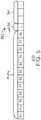
- Fig. 11is a diagram illustrating pulse width modulation (PWM) encoding used in the serial sideband link.
- PWMpulse width modulation
- the techniques described hereininclude the use of PWM encoding to convey 1 bit using two logic levels. Depending on a ratio of widths of either logic level, a unit interval is decoded as either a 1 or a 0.
- each bitconsists of two periods: a negative voltage period followed by a positive voltage period as illustrated in Fig. 11 .
- a rising edgecan either be at one-third of an interval, as indicated at the dashed line 1102, or at two-thirds of an interval, as indicated at the dashed line 1104. If the rising edge is at the one-third interval 1102, the bit period is encoded as a binary 1. If the rising edge is at the two-thirds interval 1104, then the bit period is encoded as a binary 0.
- PWM encoding described hereinincludes self-clocking properties.
- the rise time and fall timeare defined as the time it takes for the signal to transition between about 20% and 80% signal levels of a differential output signal.
- Electrical parameters for PWMmay be illustrated in Table 5 below: Table 5 Symbol Min Max Description Voltage(mV) VFS_DC 1200 1800 Full Swing TX DC voltage with unterminated TX. Resistance( ⁇ ) R 40 60 Single ended output resistance. Bit Duration (us) TPWM_BIT 1/36 1/12 PWM transmit bit duration
- Fig. 12is a diagram illustrating a cascaded switch hierarchy implemented with serial sideband links.
- Serial sideband links 1202, 1204, 1206, 1208, 1210, and 1212are implemented between endpoints 1214, 1216, and 1218, as well as switches 1220 and 1222, and a root complex 1224 in a PCIe implementation.
- a sideband linksuch as any one of the serial sideband links 1202-1212, may be configured to initialize in a legacy mode where a signal lane from a downstream port and a signal lane from an upstream port are used propagate legacy PCIe packets.
- a signal lane from a downstream portis used as PERST#
- the signal lane from an upstream portis used as CLKREQ#.
- a Basic Input Output System (BIOS)(not shown) or other software associated with the switch hierarchy illustrated in Fig. 12 may be configured to detect support for the serial sideband links 1202-1212 and enable them.
- the BIOSmay be configured to detect the serial sideband link capability from a configuration bit for example.
- LTSSMLink Training and Status State Machine
- an asynchronous handshake between endpoint 1214 and switch 1222triggers a handshake between an upstream port 1228 of switch 1222 and a downstream port 1226 of switch 1220.
- the handshake triggered between the switch 1220 and the switch 1222may then trigger an asynchronous handshake between the switch 1220 and the root complex 1224 if information needs to be conveyed upstream.
- Latencies for transmitting OBFF messagesmay equal to the sum of latencies for each link.
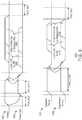
- Fig. 13is a diagram illustrating an add-in card (AIC) having pins for serial sideband signaling.
- An AIC 1302may have physical pins 1304 and 1306 operable to propagate serial sideband signals.
- An add-in card, or AIC, as referred to herein,is an expansion component configured to add functionality to a computing system when received at a system board connector 1308.
- An asynchronous handshake, as discussed above,may indicate a presence of a logical entity like the AIC 1302 at the other end of a link.
- the AIC 1302may be susceptible to hot plug and unplug events discussed above in regard to Fig 4 .
- the pins 1304 and 1306may be shorter than main band signaling pins indicated at 1310.
- the pins 1304 and 1306 of the serial sideband signalingare the last to come into physical contact with pins of the system board connector 1308 when the AIC 1302 is physically plugged into the system board connector 1308.
- the pins 1304 and 1306 associated with serial sideband signalingare the first to be removed from the pins of the system board connector 1308. This may be useful to hot plug and unplug logic 1312 of a computing system of which the system board connector 1308 is associated.
- the main band pins 1310are more likely to have already been physically received at the system board connector 1308, and the main band signaling can commence.
- removalmay preemptively indicate that a hot unplug event has occurred and main band signaling should cease.
- Fig. 14is a diagram illustrating transitions of a Link Training and Status State Machine (LTSSM) indicated on the serial sideband link.
- LTSSMLink Training and Status State Machine
- state changes in the LTSSMmay be communicated via transitions on the serial sideband link.
- an asynchronous handshakemay occur at the serial sideband link, as indicated at 1402 and 1404. This may enable deducing transitions into and out of low power states when PCIe retimers are not as robust.
- Fig. 15is diagram illustrating a retimer within a serial sideband link that is configurable by the serial sideband link.
- a retimer 1502may not be visible to software within a computing system 1504. In other words, software may only recognize a virtual link 1506 between the computing system 1504 and an AIC 1508 without the retimer 1502 in the middle. However, the retimer 1502 is visible to the serial sideband link 108, and therefore, may configure the retimer 1502.
- Fig. 16are diagrams illustrating various ways in which the serial sideband signaling may be arranged in a daisy chain fashion.
- a daisy chainas referred to herein is wiring scheme wherein multiple devices are wired together in sequence or in a ring.
- serial sideband linksare configurable to be daisy chained in a unidirectional ring.
- serial sideband linksare configurable to be daisy chained in bidirectional ring. In this manner, the serial sideband link may be enumerated, and debug testability in complex system hierarchies may be enabled.
- Fig. 17is a block diagram illustrating a method of serial sideband link signaling.
- the method 1700may include propagating, at block 1702, packets from an upstream port to a downstream port via first signaling lane of a first serial sideband link module.
- packetsare propagated from the downstream port to the upstream port via a second signaling lane of a second serial sideband link module.
- the method 1700may include initiating an asynchronous handshake via the first serial sideband link module, the second sideband link module, or both sideband link modules to wake up a serial sideband link, and performing an asynchronous handshake each time a state change is indicated for a main signaling link with which the sideband signaling is associated.
- the method 1700may also include encoding the packets propagate using pulse width modulation (PWM) without propagation of a separate clock signal.
- PWMpulse width modulation
- the method 1700includes interfacing the serial sideband link modules with one or more sideband link input/output (I/O) technologies.
Landscapes
- Engineering & Computer Science (AREA)
- Theoretical Computer Science (AREA)
- General Engineering & Computer Science (AREA)
- Physics & Mathematics (AREA)
- General Physics & Mathematics (AREA)
- Computer Hardware Design (AREA)
- Information Transfer Systems (AREA)
- Communication Control (AREA)
Description
- This disclosure relates generally to sideband signaling. Specifically, this disclosure relates to a serial sideband signaling link.
- In today's computing industry, signaling link technologies may have a main signaling link and be associated with sideband signals that are not configured to propagate over the main signaling link. Sideband link input/output (I/O) technologies provide a way for a sideband signal to be provided from one component within a computing device to another component without being propagated on the main signaling link. For example, in Peripheral Component Interconnect Express (PCIe) main signaling link technology, sideband signals may be propagated through a number of different sideband I/OP technologies such as a Card Electromechanical (CEM) sideband link, a mini CEM, a System Management Bus (SMBus), and the like. However, many times motherboard manufacturers may desire to modify existing sideband technologies by using glue logic. Glue logic, as referred to herein, is one or more custom logic modifications made to a sideband signaling link. In some cases, glue logic is difficult to implement with existing sideband I/O technologies as design and operation of these technologies may be sophisticated in comparison to the glue logic.
- The present invention is defined by the appended claims.
Fig. 1 illustrates a block diagram of serial sideband links between an upstream port and a downstream port;Fig 2 illustrates a number of scenarios where a serial sideband link consolidates sideband signals;Fig. 3 is a diagram illustrating timing of an asynchronous handshake;Fig. 4 is a diagram illustrating various packet formats of the serial sideband link;Fig. 5 is a diagram illustrating a profile negotiation packet;Fig. 6 is a diagram illustrating an example packet format for a CEM profile;Fig. 7A andFig. 7B are diagrams illustrating profile negotiation on the serial sideband link;Fig. 8 is a diagram illustrating a serial bit stream of the serial sideband link;Fig. 9 is a diagram illustrating a packet exchange on the serial sideband link;Fig. 10 is a diagram illustrating a sample implementation of a serial sideband link module;Fig. 11 is a diagram illustrating pulse width modulation (PWM) encoding used in the serial sideband link;Fig. 12 is a diagram illustrating a cascaded switch hierarchy implemented with serial sideband links;Fig. 13 is diagram illustrating a retimer within a serial sideband link that is configurable by the serial sideband link;Fig. 14 is a diagram illustrating transitions of a Link Training and Status State Machine (LTSSM) indicated on the serial sideband link;Fig. 15 is diagram illustrating a retimer within a serial sideband link that is configurable by the serial sideband link;Fig. 16 are diagrams illustrating various ways in which the serial sideband signaling may be arranged in a daisy chain fashion; andFig. 17 is a block diagram illustrating a method of serial sideband link signaling.- In some cases, the same numbers are used throughout the disclosure and the figures to reference like components and features. Numbers in the 100 series refer to features originally found in
Fig. 1 ; numbers in the 200 series refer to features originally found inFig. 2 ; and so on. - The techniques described herein include a serial sideband link. The serial sideband link includes a first serial sideband link module configured to propagate signals in one direction, and a second serial sideband link module configured to propagate signals in another direction. In embodiments, the serial sideband link may be used to consolidate other sideband link I/O technologies, such as CEM, Mini CEM, and the like, into a single serial sideband link, thereby potentially reducing pin count on any given connected components. The serial sideband link may also enable a scalable number of sideband signals to be added without adding pin count.
Fig. 1 illustrates a block diagram of serial sideband links between an upstream port and a downstream port. Anupstream port 102 may be communicatively coupled to adownstream port 104 via amain signaling link 106. Sideband signals may be propagated over a serialsideband signaling link 108. As illustrated inFig. 1 , sideband signals may be propagated in one direction by a first serialsideband link module 110, and in an opposite direction by a second serialsideband link module 112.- For example, the
main signaling link 106 may be a PCIe fabric, and sideband signals are propagated on the serialsideband signaling link 108. In embodiments, thedownstream port 104 is a controller, such as a system on chip (SoC), and theupstream port 102 may be a device, such as an expansion card communicatively coupled to a SoC. - In any case, the first serial
sideband link module 110 is to propagate signals from theupstream port 102 to thedownstream port 104 on afirst signaling lane 114. The second serialsideband link module 112 is to propagate signals from thedownstream port 104 to theupstream port 102 via asecond signaling lane 116. Fig 2 illustrates a number of scenarios where a serial sideband link consolidates sideband signals. At 202, aSoC 204 is communicatively coupled to adevice 206 through theserial sideband link 108. However, rather than being directly connected, thedevice 206 may be connected to one or more sideband link I/O technologies via aconnector 208. Theconnector 208 may be a connecter associated with sideband link technologies such as CEM, mini CEM, SMBus, and the like. In other words, theserial sideband link 108 is backwards compatible to other legacy sideband technologies, as well as any further sideband technologies. As indicated by the dashed line, theserial sideband link 108 may convert voltages to a 1.8 volt (V) domain that is compatible with theSoC 204 atglue logic 210. At 212,glue logic 210 may be disposed on either side of theconnector 208, and theserial sideband link 108 may be used on either side of theglue logic 210.- In some cases, glue logic may not be used to connect the connector to the
serial sideband link 108, as indicated at 214. In this scenario, theserial sideband link 108 may directly interface with theconnector 208. In yet other cases, theserial sideband link 108 may communicatively couple theSoC 204 to thedevice 206 via integrated components of theserial sideband link 108 within theSoC 204 and thedevice 206, as indicated at 216. Fig. 3 is a diagram illustrating timing of an asynchronous handshake. Theserial sideband link 108 may be in an idle state, and either side can be clock and/or power gated. An asynchronous handshake performed on either side of the link may be used to wake up a remote side. If either side is clock and/or power gated, this asynchronous handshake should be used to start the phase locked loops (PLLs) and establish stable power and clocks in order to correctly receive a serial bit stream on theserial sideband link 108.- As illustrated in
Fig. 3 , the side that initiates the asynchronous handshake may be referred to herein as an initiator, indicated at 302, and the side that receives the asynchronous handshake may be referred to herein as a responder, indicated at 304. Theinitiator 302 and theresponder 304 may be either upstream ports, or downstream ports, such as theports Fig. 1 . - The
initiator 302 initiates the asynchronous handshake by asserting a sideband signal of a predetermined high voltage. Theresponder 304 acknowledges the start of the asynchronous handshake by asserting a sideband signal of the predetermined high voltage. Theinitiator 302 keeps the signal asserted for a first time period, indicated by TMIN_ACTIVE inFig. 3 . Both theinitiator 302 and theresponder 304 are configured to de-assert their sideband signals any time after TMIN_ACTIVE. It is assumed that either side de-asserts their respective predetermined high voltage only when all required clocks are active and stable. - A byte value is transmitted using pulse width modulation (PWM) encoding to help the
responder 304 recover a clock, as indicated at 306. In embodiments, the byte value is an 8 bit value, wherein the first seven bits are of a value of 1 and the last bit is of a value of 0. This simple value may enable relatively quick clock recovery. A profile negotiation, and/or a serial sideband signal packet may follow, as indicated at 308. If the serial sideband link is idle for a second time period, indicated by TMAX_IDLE inFig. 3 and a sideband packet has to be transmitted, then the asynchronous handshake is repeated. - In some scenarios, both sides may initiate a handshake simultaneously. In this case, an upstream port, such as the
upstream port 102 ofFig. 1 , and a downstream port, such as thedownstream port 104 ofFig. 1 , initiate the handshake by asserting the predetermined high voltage on the serial sideband link associated with each port, respectively. Bothports downstream port 104 and theupstream port 102 are configured to de-assert their sideband signals any time after TMIN_ACTIVE. It is assumed that either side de-asserts only when all the clocks of the respective port are active and stable in either separate reference clock or common clock configurations. - A byte value is transmitted using PWM encoding to help either side recover a clock, as indicated at 310. In embodiments, the byte value is an 8 bit value, wherein the first seven bits are of a value of 1 and the last bit is of a value of 0. A profile negotiation, and/or a serial sideband signal packet may follow, as indicated at 312. If the serial sideband link is idle for a second time period, indicated by TMAX_IDLE in
Fig. 3 and a sideband packet is to be transmitted, then the asynchronous handshake is repeated. Fig. 4 is a diagram illustrating various packet formats of the serial sideband link. The various packet formats include aprofile negotiation 402, sideband signals for afixed profile 404, sideband signals for adynamic profile 406, an acknowledgement (ACK)packet 408, a non-acknowledgement (NAK)packet 410, and the like. The packet format fields may be indicated in Table 1 below:Table 1 Field Name Description SOP Start of Packet (2'b10) PROFILE ID 16 bit profile register indication support for or the selected profile P Odd parity bit for the entire packet excluding SOP and EOP EOP End of Packet (2'b01) - In some scenarios, the asynchronous handshake, as discussed above, may be used during power on reset, hot plug events, and the like. A hot plug event may also include a hot unplug event. Hot plug and hot unplug events include adding or removing components, such as an
upstream port 102 of an expansion card, from connection with adownstream port 104 without prior indication. In these scenarios, an asynchronous handshake may be performed, and a profile negotiation may follow, as discussed in more detail below. If either side does not support certain bits in a given profile, they are to be ignored by the receiving side. - The
serial sideband link 108 may be configured to perform a profile negotiation every time there is a hot plug event, state changes, or any combination thereof. In these circumstances, a profile negotiation is performed following the very first asynchronous handshake after these events. Fig. 5 is a diagram illustrating a profile negotiation packet. Each end of the serial sideband link, such as theserial sideband link 108 ofFig. 1 , is configured to maintain a 16 bit register indicating support for various profiles that may be supported by each end. Profiles are used to enable operation across various use cases such as different form factors, I/O technologies, SoC designs, and the like. Each profile defines a certain set of sideband signals. The one or more profiles to be used during serial sideband link operation may be negotiated only once during initialization out of reset. The profile negotiation is discussed below in regard toFig. 7A andFig. 7B .- As illustrated in
Fig. 5 , the profile negotiation packet may also include an "L" value indicating whether a port is transmitting a last profile of a plurality of profiles supported, indicated at 502. An example of the fields in the register is indicated in Table 2 below:Table2 Profile ID Description S0-P0 CEM S0-P1 Mini CEM S0-P2 M.2 S0-P3 SFF S0-P4 Retimer S0-P5 to S0-P15 Reserved S1-Px to S7-Px - As illustrated in Table 2, existing sideband link I/O technologies may be identified in the profile register of the
serial sideband link 108. In embodiments, the identification is performed by logic of the one or more of the serialsideband link modules Fig. 1 . As further illustrated in Table 2, the serial sideband link techniques discussed herein may be scalable to add additional sideband link I/O technologies in profile ID fields 6-15. Fig. 6 is a diagram illustrating an example packet format for a CEM profile. As discussed above in regard toFig. 5 , existing sideband link I/O technologies may be identified by theserial sideband link 108. For example, theserial sideband link 108 ofFig. 1 may identify CEM as an existing sideband link technology communicatively coupled to theserial sideband link 108. The CEM may use Optimized Buffer Flush/Fill (OBFF) toggle mechanisms of a single pin. Theserial sideband link 108 may, via a serialsideband link module serial sideband link 108.- A
packet format 602 of theserial sideband link 108 is illustrated inFig. 6 . The CEM profile details may be illustrated by Table 3 below:Table 3 Serial Bits D2U_P0 U2D_P0 Description b0 OBFF bit 1 - 4 OBFF messages encoded in a binary code b1 OBFF bit 0 - b2 CLKREQ# CLKREQ# Clock request b3 WAKE# Wake signal b4 PERST# - Fundamental Reset - As illustrated in Table 3, OBFF messages have been encoded as a 2 bit code instead of relying on rising and falling edges. Different values in the profile bits may lead to different number of bits causing different sideband signals to be propagated on the
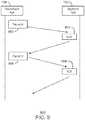
serial sideband link 108. Fig. 7A andFig. 7B are diagrams illustrating profile negotiation on the serial sideband link. As discussed above, after the asynchronous handshake, a profile negotiation may occur. The profile negotiation determines the one or more profiles available at each port, such as theupstream port 102 and thedownstream port 104 ofFig. 1 . The profile determination defines the sideband signals in the packets that are exchanged. The profile negotiation takes place immediately following a byte value, such as thebyte value 306, propagated as discussed above in regard toFig. 3 .- As illustrated in
Fig. 7A , a downstream port, such as thedownstream port 104 ofFig. 1 , sends a profile negotiation packet with a value of 1 set in all the profiles that it supports, as indicated at 702. The packet is received at an upstream port, such as theupstream port 102 ofFig. 1 . Theupstream port 102 transmits an acknowledgement (ACK) packet, as indicated at 704, upon successfully receiving a profile negotiation packet. - In some embodiments, the
downstream port 104 may be configured to refrain from transmitting another profile negotiation packet until it receives an ACK packet for the last profile negotiation packet it has transmitted at 702. If thedownstream port 104 receives a non-acknowledgement (NAK) packet, or after two milliseconds, the same profile negotiation packet will be retransmitted. - In some cases, the
downstream port 104 is configured to transmit a value of 0 in an "L" field, such the L field indicated inFig. 5 . Thedownstream port 104 is configured to transmit the value of 1 in the L field if there are more sets to be transmitted. Thedownstream port 104 sets a value of 1 in field L field it is transmitting a final profile of a plurality of profiles supported by thedownstream port 104, as indicated at 706. - After receiving the final profile of the plurality of profiles from the
downstream port 104, the upstream port may be configured to transit an ACK packet as indicated at 708. Theupstream port 102 may be further configured to transmit a profile negotiation packet, as indicated at 710, indicating one or more profiles supported by theupstream port 102. At 712, thedownstream port 104 may be configured to send an ACK packet. Similar to thedownstream port 104, the upstream port may be configured to send a plurality of profile negotiation packets, wherein a value of 1 will indicate a last profile in supported by theupstream port 102, as indicated at 714. - The profile negotiation continues at
Fig. 7B , wherein at 716, thedownstream port 104 may be configured to send an ACK packet, upon receiving the last profile supported by theupstream port 102. Thedownstream port 104 may be configured to determine which profile, or profiles, to use for transmission, as indicated at 718. Thedownstream port 104 may transmit a profile negotiation packet at 720, or a plurality of profile negotiation packets until a last profile negotiation packet at 722, , with a value of 1 set only in those profiles which are to be used for the serial sideband link operation, whereupon theupstream port 102 is configured to transmit an ACK packet back to the downstream port, as indicated at 724 in the case of a single profile packet, or at 726 in the case of multiple profile packets transmitted from thedownstream port 104. - Referring back to
Fig. 5 , the profile support package may be illustrated in Table 4 below:Table 4 Field Description b0-b2 Set: This 3 bit field defines 8 sets. Each set may have up to 12 profiles SO-Active S1-S7-Reserved b3 Last Set: This bit is used during profile negotiation. This bit does not have any meaning during any other part of the link operation. If set this bit indicates that the current set being sent is the last set. b4-b15 Profile: This 12 bit register is used to indicate support for 12 different profiles. A value of 1 in any bit indicates support for that particular profile. More than 1 bit may be set to indicate support for multiple profiles. For e.g.: b4 - indicates support for profile P0 - As illustrated in Table 4, a set of profiles may be identified in the 3 bit field defining 8 sets, and wherein each set may have up to 12 profiles.
Fig. 8 is a diagram illustrating a serial bit stream of the serial sideband link. A serial sideband link, such as theserial sideband link 108 ofFig. 1 , does not send a separate clock signal on theserial sideband link 108. This simplifies the signaling and enables for consolidation of sideband signaling technologies. Instead, PWM encoding is used to help with clock recovery and correct decoding of the bits. PWM encoding and PWM decoding require small hardware resources and may be more robust than signaling technologies requiring a forwarded clock, such as Non-Return to Zero (NRZ) encoding.- The
serial sideband link 108 is idle when no signals are being sent. A start symbol, or start of packet (SOP), is sent to start the transmission followed by sideband signals having high latency sensitivity in comparison to other sideband signals. Based on the profile selected, some of the bits will have a predefined meaning. For example, the SOP may have a value of 2'b01, indicated at 802. The bits b0 to bn01 are then configured to have a predefined meaning. The packet may then end with a stop symbol with a value of 2'b10, as indicated at 804. Fig. 9 is a diagram illustrating a packet exchange on the serial sideband link. In embodiments, to keep the serial sideband signals simple, yet reliable, a one bit parity bit included in each packet. This bit maintains an odd or even parity for the entire packet excluding the SOP and end of packet (EOP) fields. For example, if the parity bit is set to an odd parity, then if a receiving end receives a packet with a parity bit that is odd, the receiving end will send an acknowledgement (ACK) packet. If the receiving end received a parity bit that is even, the receiving end will receive a non-acknowledgement (NAK) packet back to the transmitting end. Upon receiving a NAK, the transmitting end will send a new packet with the latest value of serial sideband signals.- For example, a transmitting end may be a downstream port, such as the
downstream port 104 ofFig. 1 , and the receiving end may be an upstream port, such as the upstream port ofFig. 1 . Thedownstream port 104 may send apacket 0 to theupstream port 102, as indicated at 902. If the parity value does not match a predetermined parity between the two ports, the upstream port will return a NAK packet, as indicated at 904. At 906, thedownstream port 104 will send a new packet with the latest value of serial sideband signals to theupstream port 102. Upon determining a correct parity value, theupstream port 104 will send and ACK packet back to thedownstream port 104. Fig. 10 is a diagram illustrating a sample implementation of a serial sideband link module. A serialsideband link module 1002 is configured to receive signals from an existing connector (now shown), as indicated at 1004, and transmit signals to the existing connector, as indicated at 1006. In this example illustration, the serialsideband link module 1002 is implemented having a Serial In Parallel Out (SIPO) architecture. Theblocks Block 1012 may include combinatorial logic, at least partially comprising hardware logic, configured to implement the ACK and NAK signaling discussed above in regard toFig. 9 .- As illustrated in
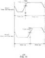
Fig. 10 , the serialsideband link module 1002 may have additional submodules including aPWM decoding module 1014, a transmission (TX) multiplexing (MUX)module 1016, and aPWM encoding module 1018. Each of thePWM decoding module 1014, theTX MUX module 1016, and thePWM decoding module 1018, may be implemented as a mix of both combinatorial logic and electrical flops or latches. Fig. 11 is a diagram illustrating pulse width modulation (PWM) encoding used in the serial sideband link. As discussed in many references above, the techniques described herein include the use of PWM encoding to convey 1 bit using two logic levels. Depending on a ratio of widths of either logic level, a unit interval is decoded as either a 1 or a 0.- For example, each bit consists of two periods: a negative voltage period followed by a positive voltage period as illustrated in
Fig. 11 . A rising edge can either be at one-third of an interval, as indicated at the dashedline 1102, or at two-thirds of an interval, as indicated at the dashedline 1104. If the rising edge is at the one-third interval 1102, the bit period is encoded as abinary 1. If the rising edge is at the two-thirds interval 1104, then the bit period is encoded as abinary 0. - It may be important to note that PWM encoding described herein includes self-clocking properties. The rise time and fall time are defined as the time it takes for the signal to transition between about 20% and 80% signal levels of a differential output signal. Electrical parameters for PWM may be illustrated in Table 5 below:
Table 5 Symbol Min Max Description Voltage(mV) VFS_DC 1200 1800 Full Swing TX DC voltage with unterminated TX. Resistance(Ω) R 40 60 Single ended output resistance. Bit Duration (us) TPWM_BIT 1/36 1/12 PWM transmit bit duration - In some cases, the serial sideband link described above is configured to operate at 19.2 MegaTransfers per second (MT/s). In this scenario, one unit interval will be 52 nanoseconds (ns). If the encode/decode logic is running a 100 Megahertz (MHz) clock, 1 clock cycle will be about 10 ns. Assuming one flop stage on the transmit side as well as the receive side, a total latency for encoding, transmitting, and
decoding 1 bit may be about TLAT_BIT defined inEquation 1 below:
Fig. 12 is a diagram illustrating a cascaded switch hierarchy implemented with serial sideband links.Serial sideband links endpoints switches root complex 1224 in a PCIe implementation.- During initial power on, a sideband link, such as any one of the serial sideband links 1202-1212, may be configured to initialize in a legacy mode where a signal lane from a downstream port and a signal lane from an upstream port are used propagate legacy PCIe packets. For example, a signal lane from a downstream port is used as PERST#, and the signal lane from an upstream port is used as CLKREQ#. A Basic Input Output System (BIOS) (not shown) or other software associated with the switch hierarchy illustrated in
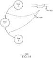
Fig. 12 may be configured to detect support for the serial sideband links 1202-1212 and enable them. The BIOS may be configured to detect the serial sideband link capability from a configuration bit for example. As a Link Training and Status State Machine (LTSSM) associated with the hierarchy goes to Detect, Disabled, L1, L2, or after power on reset the asynchronous handshake for the serial sideband link described above is performed. In some scenarios, profile negotiation is performed in Detect and after power on reset. - In the example illustration of
Fig. 12 , an asynchronous handshake betweenendpoint 1214 andswitch 1222 triggers a handshake between anupstream port 1228 ofswitch 1222 and adownstream port 1226 ofswitch 1220. The handshake triggered between theswitch 1220 and theswitch 1222 may then trigger an asynchronous handshake between theswitch 1220 and theroot complex 1224 if information needs to be conveyed upstream. Latencies for transmitting OBFF messages may equal to the sum of latencies for each link. Fig. 13 is a diagram illustrating an add-in card (AIC) having pins for serial sideband signaling. AnAIC 1302 may havephysical pins 1304 and 1306 operable to propagate serial sideband signals. An add-in card, or AIC, as referred to herein, is an expansion component configured to add functionality to a computing system when received at asystem board connector 1308. An asynchronous handshake, as discussed above, may indicate a presence of a logical entity like theAIC 1302 at the other end of a link.- In some cases, the
AIC 1302 may be susceptible to hot plug and unplug events discussed above in regard toFig 4 . In the embodiments described herein, thepins 1304 and 1306 may be shorter than main band signaling pins indicated at 1310. In this case, thepins 1304 and 1306 of the serial sideband signaling are the last to come into physical contact with pins of thesystem board connector 1308 when theAIC 1302 is physically plugged into thesystem board connector 1308. Further, when theAIC 1302 is physically removed thepins 1304 and 1306 associated with serial sideband signaling are the first to be removed from the pins of thesystem board connector 1308. This may be useful to hot plug and unpluglogic 1312 of a computing system of which thesystem board connector 1308 is associated. Specifically, when thepins 1304 and 1306 are physically received at thesystem board connector 1308 in a hot plug event, the main band pins 1310 are more likely to have already been physically received at thesystem board connector 1308, and the main band signaling can commence. Likewise, during a hot unplug event, removal may preemptively indicate that a hot unplug event has occurred and main band signaling should cease. Fig. 14 is a diagram illustrating transitions of a Link Training and Status State Machine (LTSSM) indicated on the serial sideband link. As discussed above with regard toFig. 12 , state changes in the LTSSM may be communicated via transitions on the serial sideband link. Each time the LTSSM state changes, an asynchronous handshake may occur at the serial sideband link, as indicated at 1402 and 1404. This may enable deducing transitions into and out of low power states when PCIe retimers are not as robust.Fig. 15 is diagram illustrating a retimer within a serial sideband link that is configurable by the serial sideband link. Aretimer 1502 may not be visible to software within acomputing system 1504. In other words, software may only recognize avirtual link 1506 between thecomputing system 1504 and anAIC 1508 without theretimer 1502 in the middle. However, theretimer 1502 is visible to theserial sideband link 108, and therefore, may configure theretimer 1502.Fig. 16 are diagrams illustrating various ways in which the serial sideband signaling may be arranged in a daisy chain fashion. A daisy chain, as referred to herein is wiring scheme wherein multiple devices are wired together in sequence or in a ring. For example, at 1602, serial sideband links are configurable to be daisy chained in a unidirectional ring. At 1604, serial sideband links are configurable to be daisy chained in bidirectional ring. In this manner, the serial sideband link may be enumerated, and debug testability in complex system hierarchies may be enabled.Fig. 17 is a block diagram illustrating a method of serial sideband link signaling. Themethod 1700 may include propagating, atblock 1702, packets from an upstream port to a downstream port via first signaling lane of a first serial sideband link module. Atblock 1704, packets are propagated from the downstream port to the upstream port via a second signaling lane of a second serial sideband link module.- Other method steps are considered. For example, the
method 1700 may include initiating an asynchronous handshake via the first serial sideband link module, the second sideband link module, or both sideband link modules to wake up a serial sideband link, and performing an asynchronous handshake each time a state change is indicated for a main signaling link with which the sideband signaling is associated. Themethod 1700 may also include encoding the packets propagate using pulse width modulation (PWM) without propagation of a separate clock signal. In some cases, themethod 1700 includes interfacing the serial sideband link modules with one or more sideband link input/output (I/O) technologies.

Claims (13)
- An apparatus for sideband signaling, comprising:a first serial sideband link module (110) to propagate packets from an upstream port (102) to a downstream port (104) via a first signaling lane (114);a second serial sideband link module (112) to propagate packets from the downstream port (104) to the upstream port (102) via a second signaling lane (116),characterized in that:
each of the first serial sideband link module (110) and the second sideband link module (112) comprise a 16-bit register to identify support for a plurality of profiles to enable operation across various sideband link I/O technologies. - The apparatus for sideband signaling of claim 1, wherein an
asynchronous handshake is initiated by the first serial sideband link module (110), the second serial sideband link module (112), or both sideband link modules to wake up a serial sideband link. - The apparatus for sideband signaling of any combination of claims 1 -2, wherein the packets propagate using pulse width modulation (PWM) encoding without propagation of a separate clock signal.
- The apparatus for sideband signaling of any combination of claims 1 -2, wherein the sideband signaling is asynchronous.
- The apparatus for sideband signaling of any combination of claims 1 -2, wherein the signaling lanes are connected to Universal Serial Bus (USB) future use pins.
- The apparatus for sideband signaling of any combination of claims 1 -2, wherein the apparatus is to connect to one or more apparatuses for sideband signaling in a daisy chain configuration.
- The apparatus for sideband signaling of any combination of claims 1 -2, wherein an asynchronous handshake received at the second serial sideband link module (112) indicates a presence of a logical entity at another port.
- The apparatus for sideband signaling of any combination of claims 1 -2, wherein the sideband link signaling is communicated over a connector comprising pins associated with the sideband link that are shorter than other pins of the connector.
- The apparatus for sideband signaling of any combination of claims 1-2, wherein the sideband link modules are to communicate state changes for a main signaling link with which the sideband signaling is associated by performing an asynchronous handshake each time a state change is indicated.
- A method for sideband signaling, the method comprising:interfacing serial sideband link modules with one or more sideband link input/output (I/O) technologies;propagating packets from an upstream port (102) to a downstream port (104) via first signaling lane (114) of a first serial sideband link module (110);propagating packets from the downstream port (104) to the upstream port (102) via a second signaling lane (116) of a second serial sideband link module (112),characterized in that:
each of the first serial sideband link module (110) and the second sideband link module (112) comprise a 16-bit register to identify support for a plurality of profiles to enable operation across various sideband link I/O technologies. - The method for sideband signaling of claim 11, comprising initiating an asynchronous handshake via the first serial sideband link module, the second sideband link module, or both sideband link modules to wake up a serial sideband link.
- The method for sideband signaling of any combination of claims 11 - 12, comprising encoding the packets propagate using pulse width modulation (PWM) without propagation of a separate clock signal.
- The method for sideband signaling of any combination of claims 11 - 12, comprising connecting each of the signaling lanes to one or more additional sideband signaling in a daisy chain configuration.
Applications Claiming Priority (2)
| Application Number | Priority Date | Filing Date | Title |
|---|---|---|---|
| MYPI2014702585AMY175303A (en) | 2014-09-11 | 2014-09-11 | Apparatus for sideband signaling, method for sideband signaling and system for sideband signaling |
| PCT/US2014/072389WO2016039791A1 (en) | 2014-09-11 | 2014-12-24 | Serial sideband signaling link |
Publications (3)
| Publication Number | Publication Date |
|---|---|
| EP3191969A1 EP3191969A1 (en) | 2017-07-19 |
| EP3191969A4 EP3191969A4 (en) | 2018-04-18 |
| EP3191969B1true EP3191969B1 (en) | 2020-11-11 |
Family
ID=55459394
Family Applications (1)
| Application Number | Title | Priority Date | Filing Date |
|---|---|---|---|
| EP14901804.6AActiveEP3191969B1 (en) | 2014-09-11 | 2014-12-24 | Serial sideband signaling link |
Country Status (8)
| Country | Link |
|---|---|
| US (1) | US20170235701A1 (en) |
| EP (1) | EP3191969B1 (en) |
| JP (1) | JP6428913B2 (en) |
| KR (1) | KR102243771B1 (en) |
| CN (1) | CN106575269B (en) |
| BR (1) | BR112017002551B1 (en) |
| MY (1) | MY175303A (en) |
| WO (1) | WO2016039791A1 (en) |
Families Citing this family (11)
| Publication number | Priority date | Publication date | Assignee | Title |
|---|---|---|---|---|
| US10387346B2 (en)* | 2016-05-06 | 2019-08-20 | Quanta Computer Inc. | Dynamic PCIE switch reconfiguration mechanism |
| US10127184B2 (en) | 2016-09-27 | 2018-11-13 | Intel Corporation | Low overheard high throughput solution for point-to-point link |
| US10860449B2 (en)* | 2017-03-31 | 2020-12-08 | Intel Corporation | Adjustable retimer buffer |
| US11249808B2 (en) | 2017-08-22 | 2022-02-15 | Intel Corporation | Connecting accelerator resources using a switch |
| CN109491951B (en)* | 2018-09-28 | 2022-05-10 | 超聚变数字技术有限公司 | Data configuration method and computing equipment |
| JP7490947B2 (en)* | 2019-04-08 | 2024-05-28 | 株式会社リコー | Expansion module, module system, and computer system |
| US12392824B2 (en)* | 2021-10-28 | 2025-08-19 | Intel Corporation | System, apparatus and method for communicating debug messages on a sideband of a serial link according to a debug type messaging protocol |
| US12079055B2 (en) | 2022-09-21 | 2024-09-03 | Qualcomm Incorporated | Input-output voltage control for data communication interface |
| US12386382B2 (en)* | 2023-06-05 | 2025-08-12 | Qualcomm Incorporated | Reduced training for main band chip module interconnection clock lines |
| US12430280B2 (en) | 2023-09-13 | 2025-09-30 | Qualcomm Incorporated | Mechanism to improve the reliability of sideband in chiplets |
| US12399853B2 (en)* | 2023-12-14 | 2025-08-26 | Qualcomm Incorporated | Mechanism to improve link initialization time |
Family Cites Families (15)
| Publication number | Priority date | Publication date | Assignee | Title |
|---|---|---|---|---|
| US7404032B2 (en)* | 2000-01-05 | 2008-07-22 | Rambus Inc. | Configurable width buffered module having switch elements |
| US8837471B2 (en)* | 2001-08-01 | 2014-09-16 | Certicom Corp. | Disabling header compression over point-to-point protocol (PPP) |
| US7225247B2 (en)* | 2002-10-17 | 2007-05-29 | Intel Corporation | Serial port redirection using a management controller |
| US7111102B2 (en)* | 2003-10-06 | 2006-09-19 | Cisco Technology, Inc. | Port adapter for high-bandwidth bus |
| KR101110625B1 (en)* | 2005-03-09 | 2012-02-16 | 삼성전자주식회사 | Method and apparatus for checking integrity of transmission data |
| US7680973B2 (en)* | 2007-06-08 | 2010-03-16 | Igt | Sideband signal for USB with interrupt capability |
| US7546409B2 (en)* | 2007-06-28 | 2009-06-09 | Intel Corporation | Deferring peripheral traffic with sideband control |
| US8244951B2 (en)* | 2008-09-25 | 2012-08-14 | Intel Corporation | Method and apparatus to facilitate system to system protocol exchange in back to back non-transparent bridges |
| US7934045B2 (en)* | 2009-06-09 | 2011-04-26 | International Business Machines Corporation | Redundant and fault tolerant control of an I/O enclosure by multiple hosts |
| US8850250B2 (en)* | 2010-06-01 | 2014-09-30 | Intel Corporation | Integration of processor and input/output hub |
| CN102547865B (en)* | 2010-12-23 | 2014-07-16 | 工业和信息化部电信传输研究所 | Asymmetric carrier aggregation method |
| JP2012146041A (en)* | 2011-01-11 | 2012-08-02 | Hitachi Ltd | Computer device and signal transmission method |
| US9122481B2 (en)* | 2011-07-01 | 2015-09-01 | Qualcomm Incorporated | System and method for standby power reduction in a serial communication system |
| US8549205B1 (en)* | 2012-05-22 | 2013-10-01 | Intel Corporation | Providing a consolidated sideband communication channel between devices |
| US8972640B2 (en)* | 2012-06-27 | 2015-03-03 | Intel Corporation | Controlling a physical link of a first protocol using an extended capability structure of a second protocol |
- 2014
- 2014-09-11MYMYPI2014702585Apatent/MY175303A/enunknown
- 2014-12-24USUS15/503,097patent/US20170235701A1/ennot_activeAbandoned
- 2014-12-24KRKR1020177003582Apatent/KR102243771B1/enactiveActive
- 2014-12-24JPJP2017505820Apatent/JP6428913B2/enactiveActive
- 2014-12-24EPEP14901804.6Apatent/EP3191969B1/enactiveActive
- 2014-12-24WOPCT/US2014/072389patent/WO2016039791A1/enactiveApplication Filing
- 2014-12-24BRBR112017002551-5Apatent/BR112017002551B1/enactiveIP Right Grant
- 2014-12-24CNCN201480081000.7Apatent/CN106575269B/enactiveActive
Non-Patent Citations (1)
| Title |
|---|
| None* |
Also Published As
| Publication number | Publication date |
|---|---|
| KR20170031723A (en) | 2017-03-21 |
| JP6428913B2 (en) | 2018-11-28 |
| MY175303A (en) | 2020-06-18 |
| BR112017002551A2 (en) | 2017-12-05 |
| EP3191969A4 (en) | 2018-04-18 |
| CN106575269A (en) | 2017-04-19 |
| EP3191969A1 (en) | 2017-07-19 |
| BR112017002551B1 (en) | 2023-03-21 |
| US20170235701A1 (en) | 2017-08-17 |
| KR102243771B1 (en) | 2021-04-23 |
| WO2016039791A1 (en) | 2016-03-17 |
| JP2017532627A (en) | 2017-11-02 |
| CN106575269B (en) | 2021-08-24 |
Similar Documents
| Publication | Publication Date | Title |
|---|---|---|
| EP3191969B1 (en) | Serial sideband signaling link | |
| US10180927B2 (en) | Device, system and method for communication with heterogeneous physical layers | |
| CN107580702B (en) | Enhanced virtual GPIO with multi-mode modulation | |
| US20050154946A1 (en) | Programmable measurement mode for a serial point to point link | |
| US9569390B2 (en) | Protocol for communication | |
| CN111371542B (en) | Method and apparatus for clock and data recovery for a pulse-based multiline | |
| CN106528484A (en) | Serial communication method | |
| CN107223312B (en) | Multiple modulation for data link power reduction and throughput improvement | |
| CN115203109A (en) | PCIe interface and interface system | |
| WO2017171997A1 (en) | A method, apparatus and system for communicating between multiple protocols | |
| US20160371157A1 (en) | Serial interface with bit-level acknowledgement and error correction | |
| CN108170616B (en) | A system for signal transmission across clock domains using latches | |
| US20250036518A1 (en) | Single signal debug port | |
| US8675798B1 (en) | Systems, circuits, and methods for phase inversion | |
| CN1255952C (en) | Manchester coder and decoder | |
| CN114138063B (en) | A transmission method and device for reducing connector signals based on CPLD | |
| EP4550701A1 (en) | Method for link transition in universal serial bus and system thereof | |
| Miryala | Implementation of PCS of Physical Layer for PCI Express | |
| CN115982087A (en) | Signal transmission method, computer device, and storage medium | |
| CN117112276A (en) | SPI communication detection and verification module and SPI communication system | |
| CN102880571A (en) | Synchronous serial connection device | |
| Murthy | RTL Design of PCI Express Physical Link Layer Receive Logic | |
| JP2005354158A (en) | Error detection circuit |
Legal Events
| Date | Code | Title | Description |
|---|---|---|---|
| STAA | Information on the status of an ep patent application or granted ep patent | Free format text:STATUS: THE INTERNATIONAL PUBLICATION HAS BEEN MADE | |
| PUAI | Public reference made under article 153(3) epc to a published international application that has entered the european phase | Free format text:ORIGINAL CODE: 0009012 | |
| STAA | Information on the status of an ep patent application or granted ep patent | Free format text:STATUS: REQUEST FOR EXAMINATION WAS MADE | |
| 17P | Request for examination filed | Effective date:20170201 | |
| AK | Designated contracting states | Kind code of ref document:A1 Designated state(s):AL AT BE BG CH CY CZ DE DK EE ES FI FR GB GR HR HU IE IS IT LI LT LU LV MC MK MT NL NO PL PT RO RS SE SI SK SM TR | |
| AX | Request for extension of the european patent | Extension state:BA ME | |
| DAX | Request for extension of the european patent (deleted) | ||
| RIN1 | Information on inventor provided before grant (corrected) | Inventor name:PETHE, AKSHAY Inventor name:FROELICH, DANIEL Inventor name:JAUSSI, JAMES Inventor name:WU, ZUOGUO Inventor name:HARRIMAN, DAVID Inventor name:LIM, SU WEI Inventor name:IYER, VENKATRAMAN Inventor name:WAGH, MAHESH Inventor name:DAS SHARMA, DEBENDRA | |
| A4 | Supplementary search report drawn up and despatched | Effective date:20180316 | |
| RIC1 | Information provided on ipc code assigned before grant | Ipc:G06F 13/14 20060101AFI20180312BHEP Ipc:G06F 13/38 20060101ALI20180312BHEP Ipc:G06F 13/40 20060101ALI20180312BHEP Ipc:G06F 13/42 20060101ALI20180312BHEP | |
| STAA | Information on the status of an ep patent application or granted ep patent | Free format text:STATUS: EXAMINATION IS IN PROGRESS | |
| 17Q | First examination report despatched | Effective date:20190731 | |
| GRAP | Despatch of communication of intention to grant a patent | Free format text:ORIGINAL CODE: EPIDOSNIGR1 | |
| STAA | Information on the status of an ep patent application or granted ep patent | Free format text:STATUS: GRANT OF PATENT IS INTENDED | |
| INTG | Intention to grant announced | Effective date:20200805 | |
| GRAS | Grant fee paid | Free format text:ORIGINAL CODE: EPIDOSNIGR3 | |
| GRAA | (expected) grant | Free format text:ORIGINAL CODE: 0009210 | |
| STAA | Information on the status of an ep patent application or granted ep patent | Free format text:STATUS: THE PATENT HAS BEEN GRANTED | |
| AK | Designated contracting states | Kind code of ref document:B1 Designated state(s):AL AT BE BG CH CY CZ DE DK EE ES FI FR GB GR HR HU IE IS IT LI LT LU LV MC MK MT NL NO PL PT RO RS SE SI SK SM TR | |
| REG | Reference to a national code | Ref country code:GB Ref legal event code:FG4D | |
| REG | Reference to a national code | Ref country code:CH Ref legal event code:EP | |
| REG | Reference to a national code | Ref country code:AT Ref legal event code:REF Ref document number:1334155 Country of ref document:AT Kind code of ref document:T Effective date:20201115 | |
| REG | Reference to a national code | Ref country code:DE Ref legal event code:R096 Ref document number:602014072377 Country of ref document:DE | |
| REG | Reference to a national code | Ref country code:IE Ref legal event code:FG4D | |
| PGFP | Annual fee paid to national office [announced via postgrant information from national office to epo] | Ref country code:DE Payment date:20201208 Year of fee payment:7 | |
| REG | Reference to a national code | Ref country code:NL Ref legal event code:FP | |
| PGFP | Annual fee paid to national office [announced via postgrant information from national office to epo] | Ref country code:NL Payment date:20201214 Year of fee payment:7 | |
| REG | Reference to a national code | Ref country code:AT Ref legal event code:MK05 Ref document number:1334155 Country of ref document:AT Kind code of ref document:T Effective date:20201111 | |
| PG25 | Lapsed in a contracting state [announced via postgrant information from national office to epo] | Ref country code:GR Free format text:LAPSE BECAUSE OF FAILURE TO SUBMIT A TRANSLATION OF THE DESCRIPTION OR TO PAY THE FEE WITHIN THE PRESCRIBED TIME-LIMIT Effective date:20210212 Ref country code:RS Free format text:LAPSE BECAUSE OF FAILURE TO SUBMIT A TRANSLATION OF THE DESCRIPTION OR TO PAY THE FEE WITHIN THE PRESCRIBED TIME-LIMIT Effective date:20201111 Ref country code:FI Free format text:LAPSE BECAUSE OF FAILURE TO SUBMIT A TRANSLATION OF THE DESCRIPTION OR TO PAY THE FEE WITHIN THE PRESCRIBED TIME-LIMIT Effective date:20201111 Ref country code:NO Free format text:LAPSE BECAUSE OF FAILURE TO SUBMIT A TRANSLATION OF THE DESCRIPTION OR TO PAY THE FEE WITHIN THE PRESCRIBED TIME-LIMIT Effective date:20210211 Ref country code:PT Free format text:LAPSE BECAUSE OF FAILURE TO SUBMIT A TRANSLATION OF THE DESCRIPTION OR TO PAY THE FEE WITHIN THE PRESCRIBED TIME-LIMIT Effective date:20210311 | |
| PG25 | Lapsed in a contracting state [announced via postgrant information from national office to epo] | Ref country code:PL Free format text:LAPSE BECAUSE OF FAILURE TO SUBMIT A TRANSLATION OF THE DESCRIPTION OR TO PAY THE FEE WITHIN THE PRESCRIBED TIME-LIMIT Effective date:20201111 Ref country code:IS Free format text:LAPSE BECAUSE OF FAILURE TO SUBMIT A TRANSLATION OF THE DESCRIPTION OR TO PAY THE FEE WITHIN THE PRESCRIBED TIME-LIMIT Effective date:20210311 Ref country code:LV Free format text:LAPSE BECAUSE OF FAILURE TO SUBMIT A TRANSLATION OF THE DESCRIPTION OR TO PAY THE FEE WITHIN THE PRESCRIBED TIME-LIMIT Effective date:20201111 Ref country code:SE Free format text:LAPSE BECAUSE OF FAILURE TO SUBMIT A TRANSLATION OF THE DESCRIPTION OR TO PAY THE FEE WITHIN THE PRESCRIBED TIME-LIMIT Effective date:20201111 Ref country code:BG Free format text:LAPSE BECAUSE OF FAILURE TO SUBMIT A TRANSLATION OF THE DESCRIPTION OR TO PAY THE FEE WITHIN THE PRESCRIBED TIME-LIMIT Effective date:20210211 Ref country code:AT Free format text:LAPSE BECAUSE OF FAILURE TO SUBMIT A TRANSLATION OF THE DESCRIPTION OR TO PAY THE FEE WITHIN THE PRESCRIBED TIME-LIMIT Effective date:20201111 | |
| REG | Reference to a national code | Ref country code:LT Ref legal event code:MG9D | |
| PG25 | Lapsed in a contracting state [announced via postgrant information from national office to epo] | Ref country code:HR Free format text:LAPSE BECAUSE OF FAILURE TO SUBMIT A TRANSLATION OF THE DESCRIPTION OR TO PAY THE FEE WITHIN THE PRESCRIBED TIME-LIMIT Effective date:20201111 | |
| PG25 | Lapsed in a contracting state [announced via postgrant information from national office to epo] | Ref country code:RO Free format text:LAPSE BECAUSE OF FAILURE TO SUBMIT A TRANSLATION OF THE DESCRIPTION OR TO PAY THE FEE WITHIN THE PRESCRIBED TIME-LIMIT Effective date:20201111 Ref country code:SK Free format text:LAPSE BECAUSE OF FAILURE TO SUBMIT A TRANSLATION OF THE DESCRIPTION OR TO PAY THE FEE WITHIN THE PRESCRIBED TIME-LIMIT Effective date:20201111 Ref country code:LT Free format text:LAPSE BECAUSE OF FAILURE TO SUBMIT A TRANSLATION OF THE DESCRIPTION OR TO PAY THE FEE WITHIN THE PRESCRIBED TIME-LIMIT Effective date:20201111 Ref country code:SM Free format text:LAPSE BECAUSE OF FAILURE TO SUBMIT A TRANSLATION OF THE DESCRIPTION OR TO PAY THE FEE WITHIN THE PRESCRIBED TIME-LIMIT Effective date:20201111 Ref country code:EE Free format text:LAPSE BECAUSE OF FAILURE TO SUBMIT A TRANSLATION OF THE DESCRIPTION OR TO PAY THE FEE WITHIN THE PRESCRIBED TIME-LIMIT Effective date:20201111 Ref country code:CZ Free format text:LAPSE BECAUSE OF FAILURE TO SUBMIT A TRANSLATION OF THE DESCRIPTION OR TO PAY THE FEE WITHIN THE PRESCRIBED TIME-LIMIT Effective date:20201111 | |
| REG | Reference to a national code | Ref country code:CH Ref legal event code:PL | |
| REG | Reference to a national code | Ref country code:DE Ref legal event code:R097 Ref document number:602014072377 Country of ref document:DE | |
| PG25 | Lapsed in a contracting state [announced via postgrant information from national office to epo] | Ref country code:MC Free format text:LAPSE BECAUSE OF FAILURE TO SUBMIT A TRANSLATION OF THE DESCRIPTION OR TO PAY THE FEE WITHIN THE PRESCRIBED TIME-LIMIT Effective date:20201111 Ref country code:DK Free format text:LAPSE BECAUSE OF FAILURE TO SUBMIT A TRANSLATION OF THE DESCRIPTION OR TO PAY THE FEE WITHIN THE PRESCRIBED TIME-LIMIT Effective date:20201111 | |
| REG | Reference to a national code | Ref country code:BE Ref legal event code:MM Effective date:20201231 | |
| PLBE | No opposition filed within time limit | Free format text:ORIGINAL CODE: 0009261 | |
| STAA | Information on the status of an ep patent application or granted ep patent | Free format text:STATUS: NO OPPOSITION FILED WITHIN TIME LIMIT | |
| 26N | No opposition filed | Effective date:20210812 | |
| GBPC | Gb: european patent ceased through non-payment of renewal fee | Effective date:20210211 | |
| PG25 | Lapsed in a contracting state [announced via postgrant information from national office to epo] | Ref country code:IE Free format text:LAPSE BECAUSE OF NON-PAYMENT OF DUE FEES Effective date:20201224 Ref country code:IT Free format text:LAPSE BECAUSE OF FAILURE TO SUBMIT A TRANSLATION OF THE DESCRIPTION OR TO PAY THE FEE WITHIN THE PRESCRIBED TIME-LIMIT Effective date:20201111 Ref country code:LU Free format text:LAPSE BECAUSE OF NON-PAYMENT OF DUE FEES Effective date:20201224 Ref country code:FR Free format text:LAPSE BECAUSE OF NON-PAYMENT OF DUE FEES Effective date:20210111 Ref country code:AL Free format text:LAPSE BECAUSE OF FAILURE TO SUBMIT A TRANSLATION OF THE DESCRIPTION OR TO PAY THE FEE WITHIN THE PRESCRIBED TIME-LIMIT Effective date:20201111 | |
| PG25 | Lapsed in a contracting state [announced via postgrant information from national office to epo] | Ref country code:CH Free format text:LAPSE BECAUSE OF NON-PAYMENT OF DUE FEES Effective date:20201231 Ref country code:SI Free format text:LAPSE BECAUSE OF FAILURE TO SUBMIT A TRANSLATION OF THE DESCRIPTION OR TO PAY THE FEE WITHIN THE PRESCRIBED TIME-LIMIT Effective date:20201111 Ref country code:LI Free format text:LAPSE BECAUSE OF NON-PAYMENT OF DUE FEES Effective date:20201231 | |
| PG25 | Lapsed in a contracting state [announced via postgrant information from national office to epo] | Ref country code:GB Free format text:LAPSE BECAUSE OF NON-PAYMENT OF DUE FEES Effective date:20210211 Ref country code:ES Free format text:LAPSE BECAUSE OF FAILURE TO SUBMIT A TRANSLATION OF THE DESCRIPTION OR TO PAY THE FEE WITHIN THE PRESCRIBED TIME-LIMIT Effective date:20201111 | |
| PG25 | Lapsed in a contracting state [announced via postgrant information from national office to epo] | Ref country code:IS Free format text:LAPSE BECAUSE OF FAILURE TO SUBMIT A TRANSLATION OF THE DESCRIPTION OR TO PAY THE FEE WITHIN THE PRESCRIBED TIME-LIMIT Effective date:20210311 Ref country code:TR Free format text:LAPSE BECAUSE OF FAILURE TO SUBMIT A TRANSLATION OF THE DESCRIPTION OR TO PAY THE FEE WITHIN THE PRESCRIBED TIME-LIMIT Effective date:20201111 Ref country code:MT Free format text:LAPSE BECAUSE OF FAILURE TO SUBMIT A TRANSLATION OF THE DESCRIPTION OR TO PAY THE FEE WITHIN THE PRESCRIBED TIME-LIMIT Effective date:20201111 Ref country code:CY Free format text:LAPSE BECAUSE OF FAILURE TO SUBMIT A TRANSLATION OF THE DESCRIPTION OR TO PAY THE FEE WITHIN THE PRESCRIBED TIME-LIMIT Effective date:20201111 | |
| PG25 | Lapsed in a contracting state [announced via postgrant information from national office to epo] | Ref country code:MK Free format text:LAPSE BECAUSE OF FAILURE TO SUBMIT A TRANSLATION OF THE DESCRIPTION OR TO PAY THE FEE WITHIN THE PRESCRIBED TIME-LIMIT Effective date:20201111 | |
| REG | Reference to a national code | Ref country code:DE Ref legal event code:R119 Ref document number:602014072377 Country of ref document:DE | |
| PG25 | Lapsed in a contracting state [announced via postgrant information from national office to epo] | Ref country code:BE Free format text:LAPSE BECAUSE OF NON-PAYMENT OF DUE FEES Effective date:20201231 | |
| REG | Reference to a national code | Ref country code:NL Ref legal event code:MM Effective date:20220101 | |
| PG25 | Lapsed in a contracting state [announced via postgrant information from national office to epo] | Ref country code:NL Free format text:LAPSE BECAUSE OF NON-PAYMENT OF DUE FEES Effective date:20220101 | |
| PG25 | Lapsed in a contracting state [announced via postgrant information from national office to epo] | Ref country code:DE Free format text:LAPSE BECAUSE OF NON-PAYMENT OF DUE FEES Effective date:20220701 |