EP3188224B1 - Processes and apparatus for preparing heterostructures with reduced strain by radial distension - Google Patents
Processes and apparatus for preparing heterostructures with reduced strain by radial distensionDownload PDFInfo
- Publication number
- EP3188224B1 EP3188224B1EP17154584.1AEP17154584AEP3188224B1EP 3188224 B1EP3188224 B1EP 3188224B1EP 17154584 AEP17154584 AEP 17154584AEP 3188224 B1EP3188224 B1EP 3188224B1
- Authority
- EP
- European Patent Office
- Prior art keywords
- substrate
- layer
- semiconductor structure
- dislocations
- chamber
- Prior art date
- Legal status (The legal status is an assumption and is not a legal conclusion. Google has not performed a legal analysis and makes no representation as to the accuracy of the status listed.)
- Active
Links
- 238000000034methodMethods0.000titleclaimsdescription37
- 239000000758substrateSubstances0.000claimsdescription151
- 239000004065semiconductorSubstances0.000claimsdescription76
- 230000002093peripheral effectEffects0.000claimsdescription40
- 230000006835compressionEffects0.000claimsdescription7
- 238000007906compressionMethods0.000claimsdescription7
- 239000012530fluidSubstances0.000claimsdescription7
- 238000010438heat treatmentMethods0.000claimsdescription6
- 238000004891communicationMethods0.000claimsdescription4
- 239000010410layerSubstances0.000description124
- 230000035882stressEffects0.000description40
- 239000002344surface layerSubstances0.000description39
- 239000000463materialSubstances0.000description21
- 150000002500ionsChemical class0.000description20
- 229910000577Silicon-germaniumInorganic materials0.000description14
- 239000013078crystalSubstances0.000description14
- 229910052710siliconInorganic materials0.000description14
- 239000010703siliconSubstances0.000description14
- XUIMIQQOPSSXEZ-UHFFFAOYSA-NSiliconChemical compound[Si]XUIMIQQOPSSXEZ-UHFFFAOYSA-N0.000description12
- 238000000576coating methodMethods0.000description11
- 239000010408filmSubstances0.000description10
- 229910052732germaniumInorganic materials0.000description10
- 125000004429atomChemical group0.000description9
- 239000011248coating agentSubstances0.000description9
- 238000000151depositionMethods0.000description8
- 238000000227grindingMethods0.000description6
- 230000004913activationEffects0.000description5
- 230000003247decreasing effectEffects0.000description5
- 239000007943implantSubstances0.000description5
- 229910021421monocrystalline siliconInorganic materials0.000description5
- 230000002040relaxant effectEffects0.000description5
- JBRZTFJDHDCESZ-UHFFFAOYSA-NAsGaChemical compound[As]#[Ga]JBRZTFJDHDCESZ-UHFFFAOYSA-N0.000description4
- 208000035208Ring chromosome 20 syndromeDiseases0.000description4
- LEVVHYCKPQWKOP-UHFFFAOYSA-N[Si].[Ge]Chemical compound[Si].[Ge]LEVVHYCKPQWKOP-UHFFFAOYSA-N0.000description4
- GNPVGFCGXDBREM-UHFFFAOYSA-Ngermanium atomChemical compound[Ge]GNPVGFCGXDBREM-UHFFFAOYSA-N0.000description4
- -1silicon ionsChemical class0.000description4
- 230000003313weakening effectEffects0.000description4
- 206010000060Abdominal distensionDiseases0.000description3
- QVGXLLKOCUKJST-UHFFFAOYSA-Natomic oxygenChemical compound[O]QVGXLLKOCUKJST-UHFFFAOYSA-N0.000description3
- 238000005229chemical vapour depositionMethods0.000description3
- 238000007796conventional methodMethods0.000description3
- 230000006355external stressEffects0.000description3
- 238000007373indentationMethods0.000description3
- 239000012212insulatorSubstances0.000description3
- 239000001301oxygenSubstances0.000description3
- 229910052760oxygenInorganic materials0.000description3
- HBMJWWWQQXIZIP-UHFFFAOYSA-Nsilicon carbideChemical compound[Si+]#[C-]HBMJWWWQQXIZIP-UHFFFAOYSA-N0.000description3
- 229910010271silicon carbideInorganic materials0.000description3
- XKRFYHLGVUSROY-UHFFFAOYSA-NArgonChemical compound[Ar]XKRFYHLGVUSROY-UHFFFAOYSA-N0.000description2
- 229910002601GaNInorganic materials0.000description2
- 229910001218Gallium arsenideInorganic materials0.000description2
- 229910000530Gallium indium arsenideInorganic materials0.000description2
- JMASRVWKEDWRBT-UHFFFAOYSA-NGallium nitrideChemical compound[Ga]#NJMASRVWKEDWRBT-UHFFFAOYSA-N0.000description2
- KXNLCSXBJCPWGL-UHFFFAOYSA-N[Ga].[As].[In]Chemical compound[Ga].[As].[In]KXNLCSXBJCPWGL-UHFFFAOYSA-N0.000description2
- 230000003213activating effectEffects0.000description2
- 229910021417amorphous siliconInorganic materials0.000description2
- 238000000231atomic layer depositionMethods0.000description2
- 230000015572biosynthetic processEffects0.000description2
- PMHQVHHXPFUNSP-UHFFFAOYSA-Mcopper(1+);methylsulfanylmethane;bromideChemical compoundBr[Cu].CSCPMHQVHHXPFUNSP-UHFFFAOYSA-M0.000description2
- 230000008021depositionEffects0.000description2
- 230000000694effectsEffects0.000description2
- 230000008020evaporationEffects0.000description2
- 238000001704evaporationMethods0.000description2
- 230000005669field effectEffects0.000description2
- 238000002513implantationMethods0.000description2
- 238000004519manufacturing processMethods0.000description2
- 238000010297mechanical methods and processMethods0.000description2
- 229910052594sapphireInorganic materials0.000description2
- 239000010980sapphireSubstances0.000description2
- 239000000126substanceSubstances0.000description2
- 239000010409thin filmSubstances0.000description2
- 238000012546transferMethods0.000description2
- 238000000038ultrahigh vacuum chemical vapour depositionMethods0.000description2
- 229910052582BNInorganic materials0.000description1
- PZNSFCLAULLKQX-UHFFFAOYSA-NBoron nitrideChemical compoundN#BPZNSFCLAULLKQX-UHFFFAOYSA-N0.000description1
- OKTJSMMVPCPJKN-UHFFFAOYSA-NCarbonChemical compound[C]OKTJSMMVPCPJKN-UHFFFAOYSA-N0.000description1
- 238000002231Czochralski processMethods0.000description1
- 229910010038TiAlInorganic materials0.000description1
- 229910052786argonInorganic materials0.000description1
- 229910001632barium fluorideInorganic materials0.000description1
- WUKWITHWXAAZEY-UHFFFAOYSA-Lcalcium difluorideChemical compound[F-].[F-].[Ca+2]WUKWITHWXAAZEY-UHFFFAOYSA-L0.000description1
- 229910001634calcium fluorideInorganic materials0.000description1
- 230000001143conditioned effectEffects0.000description1
- 230000001276controlling effectEffects0.000description1
- 238000001816coolingMethods0.000description1
- 230000001351cycling effectEffects0.000description1
- 230000000593degrading effectEffects0.000description1
- 238000001514detection methodMethods0.000description1
- 238000010586diagramMethods0.000description1
- 238000009826distributionMethods0.000description1
- 239000002783friction materialSubstances0.000description1
- 229910002804graphiteInorganic materials0.000description1
- 239000010439graphiteSubstances0.000description1
- 229910052734heliumInorganic materials0.000description1
- 239000001307heliumSubstances0.000description1
- SWQJXJOGLNCZEY-UHFFFAOYSA-Nhelium atomChemical compound[He]SWQJXJOGLNCZEY-UHFFFAOYSA-N0.000description1
- 229910052739hydrogenInorganic materials0.000description1
- 239000001257hydrogenSubstances0.000description1
- 125000004435hydrogen atomChemical class[H]*0.000description1
- 229910052738indiumInorganic materials0.000description1
- APFVFJFRJDLVQX-UHFFFAOYSA-Nindium atomChemical compound[In]APFVFJFRJDLVQX-UHFFFAOYSA-N0.000description1
- 238000005468ion implantationMethods0.000description1
- 239000011159matrix materialSubstances0.000description1
- 238000005259measurementMethods0.000description1
- 239000000203mixtureSubstances0.000description1
- 238000001451molecular beam epitaxyMethods0.000description1
- 229910052754neonInorganic materials0.000description1
- GKAOGPIIYCISHV-UHFFFAOYSA-Nneon atomChemical compound[Ne]GKAOGPIIYCISHV-UHFFFAOYSA-N0.000description1
- 230000007935neutral effectEffects0.000description1
- 238000002360preparation methodMethods0.000description1
- 238000003825pressingMethods0.000description1
- 238000012545processingMethods0.000description1
- 230000001105regulatory effectEffects0.000description1
- 238000005070samplingMethods0.000description1
- 238000005488sandblastingMethods0.000description1
- 229910001637strontium fluorideInorganic materials0.000description1
- FVRNDBHWWSPNOM-UHFFFAOYSA-Lstrontium fluorideChemical compound[F-].[F-].[Sr+2]FVRNDBHWWSPNOM-UHFFFAOYSA-L0.000description1
- 238000001947vapour-phase growthMethods0.000description1
- 239000011800void materialSubstances0.000description1
- 229910052724xenonInorganic materials0.000description1
- FHNFHKCVQCLJFQ-UHFFFAOYSA-Nxenon atomChemical compound[Xe]FHNFHKCVQCLJFQ-UHFFFAOYSA-N0.000description1
Images


Classifications
- H—ELECTRICITY
- H01—ELECTRIC ELEMENTS
- H01L—SEMICONDUCTOR DEVICES NOT COVERED BY CLASS H10
- H01L21/00—Processes or apparatus adapted for the manufacture or treatment of semiconductor or solid state devices or of parts thereof
- H01L21/67—Apparatus specially adapted for handling semiconductor or electric solid state devices during manufacture or treatment thereof; Apparatus specially adapted for handling wafers during manufacture or treatment of semiconductor or electric solid state devices or components ; Apparatus not specifically provided for elsewhere
- H01L21/683—Apparatus specially adapted for handling semiconductor or electric solid state devices during manufacture or treatment thereof; Apparatus specially adapted for handling wafers during manufacture or treatment of semiconductor or electric solid state devices or components ; Apparatus not specifically provided for elsewhere for supporting or gripping
- H01L21/687—Apparatus specially adapted for handling semiconductor or electric solid state devices during manufacture or treatment thereof; Apparatus specially adapted for handling wafers during manufacture or treatment of semiconductor or electric solid state devices or components ; Apparatus not specifically provided for elsewhere for supporting or gripping using mechanical means, e.g. chucks, clamps or pinches
- H01L21/68714—Apparatus specially adapted for handling semiconductor or electric solid state devices during manufacture or treatment thereof; Apparatus specially adapted for handling wafers during manufacture or treatment of semiconductor or electric solid state devices or components ; Apparatus not specifically provided for elsewhere for supporting or gripping using mechanical means, e.g. chucks, clamps or pinches the wafers being placed on a susceptor, stage or support
- H01L21/68735—Apparatus specially adapted for handling semiconductor or electric solid state devices during manufacture or treatment thereof; Apparatus specially adapted for handling wafers during manufacture or treatment of semiconductor or electric solid state devices or components ; Apparatus not specifically provided for elsewhere for supporting or gripping using mechanical means, e.g. chucks, clamps or pinches the wafers being placed on a susceptor, stage or support characterised by edge profile or support profile
- H—ELECTRICITY
- H01—ELECTRIC ELEMENTS
- H01L—SEMICONDUCTOR DEVICES NOT COVERED BY CLASS H10
- H01L21/00—Processes or apparatus adapted for the manufacture or treatment of semiconductor or solid state devices or of parts thereof
- H01L21/02—Manufacture or treatment of semiconductor devices or of parts thereof
- H01L21/04—Manufacture or treatment of semiconductor devices or of parts thereof the devices having potential barriers, e.g. a PN junction, depletion layer or carrier concentration layer
- H01L21/18—Manufacture or treatment of semiconductor devices or of parts thereof the devices having potential barriers, e.g. a PN junction, depletion layer or carrier concentration layer the devices having semiconductor bodies comprising elements of Group IV of the Periodic Table or AIIIBV compounds with or without impurities, e.g. doping materials
- H01L21/30—Treatment of semiconductor bodies using processes or apparatus not provided for in groups H01L21/20 - H01L21/26
- H01L21/322—Treatment of semiconductor bodies using processes or apparatus not provided for in groups H01L21/20 - H01L21/26 to modify their internal properties, e.g. to produce internal imperfections
- C—CHEMISTRY; METALLURGY
- C30—CRYSTAL GROWTH
- C30B—SINGLE-CRYSTAL GROWTH; UNIDIRECTIONAL SOLIDIFICATION OF EUTECTIC MATERIAL OR UNIDIRECTIONAL DEMIXING OF EUTECTOID MATERIAL; REFINING BY ZONE-MELTING OF MATERIAL; PRODUCTION OF A HOMOGENEOUS POLYCRYSTALLINE MATERIAL WITH DEFINED STRUCTURE; SINGLE CRYSTALS OR HOMOGENEOUS POLYCRYSTALLINE MATERIAL WITH DEFINED STRUCTURE; AFTER-TREATMENT OF SINGLE CRYSTALS OR A HOMOGENEOUS POLYCRYSTALLINE MATERIAL WITH DEFINED STRUCTURE; APPARATUS THEREFOR
- C30B25/00—Single-crystal growth by chemical reaction of reactive gases, e.g. chemical vapour-deposition growth
- C30B25/02—Epitaxial-layer growth
- C30B25/12—Substrate holders or susceptors
- H—ELECTRICITY
- H01—ELECTRIC ELEMENTS
- H01L—SEMICONDUCTOR DEVICES NOT COVERED BY CLASS H10
- H01L21/00—Processes or apparatus adapted for the manufacture or treatment of semiconductor or solid state devices or of parts thereof
- H01L21/02—Manufacture or treatment of semiconductor devices or of parts thereof
- H01L21/04—Manufacture or treatment of semiconductor devices or of parts thereof the devices having potential barriers, e.g. a PN junction, depletion layer or carrier concentration layer
- H01L21/18—Manufacture or treatment of semiconductor devices or of parts thereof the devices having potential barriers, e.g. a PN junction, depletion layer or carrier concentration layer the devices having semiconductor bodies comprising elements of Group IV of the Periodic Table or AIIIBV compounds with or without impurities, e.g. doping materials
- H01L21/30—Treatment of semiconductor bodies using processes or apparatus not provided for in groups H01L21/20 - H01L21/26
- H01L21/302—Treatment of semiconductor bodies using processes or apparatus not provided for in groups H01L21/20 - H01L21/26 to change their surface-physical characteristics or shape, e.g. etching, polishing, cutting
- H—ELECTRICITY
- H01—ELECTRIC ELEMENTS
- H01L—SEMICONDUCTOR DEVICES NOT COVERED BY CLASS H10
- H01L21/00—Processes or apparatus adapted for the manufacture or treatment of semiconductor or solid state devices or of parts thereof
- H01L21/67—Apparatus specially adapted for handling semiconductor or electric solid state devices during manufacture or treatment thereof; Apparatus specially adapted for handling wafers during manufacture or treatment of semiconductor or electric solid state devices or components ; Apparatus not specifically provided for elsewhere
- H01L21/67005—Apparatus not specifically provided for elsewhere
- H01L21/67011—Apparatus for manufacture or treatment
- H01L21/67092—Apparatus for mechanical treatment
- H—ELECTRICITY
- H01—ELECTRIC ELEMENTS
- H01L—SEMICONDUCTOR DEVICES NOT COVERED BY CLASS H10
- H01L21/00—Processes or apparatus adapted for the manufacture or treatment of semiconductor or solid state devices or of parts thereof
- H01L21/67—Apparatus specially adapted for handling semiconductor or electric solid state devices during manufacture or treatment thereof; Apparatus specially adapted for handling wafers during manufacture or treatment of semiconductor or electric solid state devices or components ; Apparatus not specifically provided for elsewhere
- H01L21/683—Apparatus specially adapted for handling semiconductor or electric solid state devices during manufacture or treatment thereof; Apparatus specially adapted for handling wafers during manufacture or treatment of semiconductor or electric solid state devices or components ; Apparatus not specifically provided for elsewhere for supporting or gripping
- H01L21/6838—Apparatus specially adapted for handling semiconductor or electric solid state devices during manufacture or treatment thereof; Apparatus specially adapted for handling wafers during manufacture or treatment of semiconductor or electric solid state devices or components ; Apparatus not specifically provided for elsewhere for supporting or gripping with gripping and holding devices using a vacuum; Bernoulli devices
- H—ELECTRICITY
- H01—ELECTRIC ELEMENTS
- H01L—SEMICONDUCTOR DEVICES NOT COVERED BY CLASS H10
- H01L21/00—Processes or apparatus adapted for the manufacture or treatment of semiconductor or solid state devices or of parts thereof
- H01L21/67—Apparatus specially adapted for handling semiconductor or electric solid state devices during manufacture or treatment thereof; Apparatus specially adapted for handling wafers during manufacture or treatment of semiconductor or electric solid state devices or components ; Apparatus not specifically provided for elsewhere
- H01L21/683—Apparatus specially adapted for handling semiconductor or electric solid state devices during manufacture or treatment thereof; Apparatus specially adapted for handling wafers during manufacture or treatment of semiconductor or electric solid state devices or components ; Apparatus not specifically provided for elsewhere for supporting or gripping
- H01L21/687—Apparatus specially adapted for handling semiconductor or electric solid state devices during manufacture or treatment thereof; Apparatus specially adapted for handling wafers during manufacture or treatment of semiconductor or electric solid state devices or components ; Apparatus not specifically provided for elsewhere for supporting or gripping using mechanical means, e.g. chucks, clamps or pinches
- H01L21/68714—Apparatus specially adapted for handling semiconductor or electric solid state devices during manufacture or treatment thereof; Apparatus specially adapted for handling wafers during manufacture or treatment of semiconductor or electric solid state devices or components ; Apparatus not specifically provided for elsewhere for supporting or gripping using mechanical means, e.g. chucks, clamps or pinches the wafers being placed on a susceptor, stage or support
- H01L21/6875—Apparatus specially adapted for handling semiconductor or electric solid state devices during manufacture or treatment thereof; Apparatus specially adapted for handling wafers during manufacture or treatment of semiconductor or electric solid state devices or components ; Apparatus not specifically provided for elsewhere for supporting or gripping using mechanical means, e.g. chucks, clamps or pinches the wafers being placed on a susceptor, stage or support characterised by a plurality of individual support members, e.g. support posts or protrusions
Definitions
- the present disclosurerelates generally to preparation of semiconductor heterostructures with reduced strain and, in particular, to heterostructures with a semiconductor substrate that conforms to a surface layer having a different crystal lattice constant than the substrate, thereby forming a relatively low-defect heterostructure.
- Multi-layered structurescomprising a device layer with a device quality surface and a substrate that has a different crystal lattice structure than the material of the device layer are useful for a number of different purposes.
- These multi-layered structurestypically comprise multiple layers of material having differing lattice constants. The lattice mismatch between layers causes the layers to be strained. Misfit dislocations may spontaneously form in the device layer to relax the strain between layers. Such dislocations degrade the quality and usefulness of the multi-layer semiconductor structure.
- One aspect of the present disclosureis directed to a process for relaxing the strain in a heterostructure comprising a substrate, a surface layer disposed on the substrate and an interface between the substrate and the surface layer.
- the substratecomprises a central axis, a back surface which is generally perpendicular to the central axis, and a diameter extending across the substrate through the central axis.
- a dislocation source layeris formed in the substrate. The substrate is radially distended to generate dislocations and glide the dislocations from the dislocation source layer toward the surface layer.
- Another aspect of the present disclosureis directed to a process for preparing a relaxed heterostructure.
- a surface layeris deposited on a front surface of the semiconductor substrate thereby creating a strain between the surface layer and the substrate.
- a dislocation source layeris formed in the substrate. The strain in the surface layer and the substrate is relaxed by radially distending the substrate to generate dislocations and glide the dislocations from the dislocation source layer toward the surface layer.
- a further aspect of the present disclosureis directed to an apparatus for radially distending a semiconductor structure having a front surface, a back surface and a circumferential edge.
- the apparatusincludes a structure holder comprising a top plate and a back plate for contacting the structure adjacent a circumferential edge of the structure.
- the top plateis adapted to contact the front surface of the structure and the back plate is adapted to contact the back surface of the structure.
- the top plate and back plateare further adapted to form a peripheral chamber between the top plate, back plate and circumferential edge of the structure.
- An additional aspect of the present disclosureis directed to an apparatus for radially distending a semiconductor structure having a front surface, a back surface, a circumferential edge and a central axis.
- the apparatusincludes triangular-shaped segments that point inward to a central axis. The segments are configured for movement outward from the central axis to cause the structure to distend. Fluid passageways are formed in each segment for forming a vacuum between the segment and structure.
- heterostructures with reduced strain between the substrate and a surface layer having a different lattice constant than the substratemay be prepared such as by the process of Figure 2 .
- the surface layermay also be referred to herein as an "epitaxial layer”, “heteroepitaxial layer”, “deposited film”, “film”, “heterolayer” or “deposited layer”.
- a heterostructure having a substantially relaxed surface layer and a reduced concentration of misfit dislocations, also referred to as threading dislocations,may be formed.
- the processes of the present disclosuremay include forming a dislocation source layer in a semiconductor substrate, depositing a heterolayer on the substrate before or after formation of the dislocation source layer and radially distending the heterostructure to generate (i.e., "activate") dislocations and glide the dislocations from the dislocation source layer toward the surface layer.
- the activation of the source layer and the gliding of the dislocations from the source layer toward the interface with the deposited layeroccur concurrently by applying a stress (e.g., tension) to the substrate.
- the stressmay be applied in one or more steps and in various combinations to activate and glide the dislocations, thereby plastically stretching the heterostructure.
- the heterolayermay have a crystal lattice constant, a S1 , which differs from the native crystal lattice constant of the substrate, a S to form a film on the surface of the substrate.
- the crystal lattice constant, a S1 , of the heterolayeris greater than the native crystal lattice constant of the substrate, as, such that by controlling the generating and gliding of the dislocation loops in the substrate by distention, the substrate may be plastically deformed and aligned more suitably with the crystal lattice of the film thereby allowing the film to be completely relaxed and having a reduced density of threading dislocations on the substrate.
- the methods of the present disclosurehave several advantages over conventional methods for relaxing heterolayers.
- Conventional methodscreate a large asymmetry in the stresses between the film and the substrate which leads to dislocation generation where the stresses are the greatest, i.e., the film.
- the dislocationsleave segments behind which act as degrading threading dislocations.
- Much efforthas been employed in attempting to minimize the density of such threading dislocations.
- Documents US6189591 and US5725728describe a method and an apparatus for radially distending a semiconductor structure.
- Pizzagalli et al(Phys. Rev. B 79, 045203, 2009 ) present a theoretical study about pressure effects and dislocations properties in semiconductors.
- Documents US2006091377 and DE19802977are concerned with a method for relaxing strain in a heterostructure by gliding dislocations.
- methods of the present disclosureresult in an asymmetry of stresses with the dislocation generation occurring in the substrate (e.g., by weakening the substrate and using a relatively thin film to void dislocation generation therein while weakening the substrate). This allows dislocations to be confined to the substrate while forming the misfit dislocation layer at the interface between the substrate and the film.
- external stressesmay be applied to the system to activate the dislocations. This differs from conventional methods which result in self-relaxation due to the relatively large intrinsic, internal stresses (i.e., relaxation without application of external stresses).
- the methods of the present disclosureinvolve relaxation other than by self-relaxation by weakening and application of external stress at appropriate temperatures with a relatively thin film such that self-relaxation does not occur.
- the semiconductor substrate 1may be any single crystal semiconductor material suitable for use as a substrate for supporting a surface layer such as by deposition of an epitaxial layer by chemical vapor deposition.
- the semiconductor substratemay be composed of a material selected from the group consisting of silicon, silicon carbide, sapphire, germanium, silicon germanium, gallium nitride, aluminum nitride, gallium arsenic, indium gallium arsenic or any combination thereof.
- the semiconductor substrateis composed of silicon.
- the semiconductor substrate 1may be in any shape suitable for both use as a substrate for depositing a surface layer and suitable for applying a stress to the substrate material as described in more detail below.
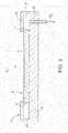
- the semiconductor substratehas a central axis 2; an interface 3 with the deposited layer 7 and a back surface 4, the substrate-surface layer interface 3 and back surface 4 being generally perpendicular to the central axis 2; a thickness t, corresponding to the distance from the interface to the back surface of the substrate; a circumferential edge 5; and a diameter D, extending across the substrate through the central axis.
- the back surface 4will be described as the opposing surface at or near which the dislocation source layer will be formed and as such may be referred to herein as the "opposing surface” and/or the “damaged surface.”
- the heterostructure itself and the deposited layer 7 described beloware generally concentric with the substrate 1 and also include a central axis 2; a circumferential edge 5; and a diameter D, extending across the heterostructure (and also the surface layer) and through the central axis.
- the substrate 1may have any suitable diameter for use as a substrate upon which a semiconductor layer will be deposited.
- the substrate 1has diameter of about 150 mm or more.
- the substrate 1has a diameter of about 200 mm or more, about 300 mm or more or even about 450 mm or more.
- the substrate diametermay be the diameter prior to plastically deforming the heterostructure, in which case, the diameter may increase from the stated values after plastic deformation as discussed in more detail below.
- the substrate prior to plastic deformationmay have a diameter less than the stated values such that the diameter after plastic deformation is approximately equal to the stated values.
- the substrate 1may have any thickness, t, suitable for use as a substrate upon which a semiconductor layer may be deposited.
- the substratemay have a thickness, t, of from about 500 microns to about 1000 microns, typically from about 600 microns to about 1000 microns, from about 700 microns to about 1000 microns, from about 700 microns to about 900 microns or even from about 700 microns to about 800 microns.
- the substrate 1may be a single crystal silicon wafer that has been sliced from a single crystal silicon ingot grown by Czochralski crystal growing methods having a diameter of about 150 mm or more, about 200 mm or more, about 300 mm or more or even about 450 mm or more and a thickness of from about 675 microns to about 1000 microns or even from about 725 microns to about 925 microns.
- the substrate surface upon which the epitaxial layer is depositedmay be polished such that it is suitable for depositing the epitaxial layer or may be further conditioned prior to chemical vapor deposition.
- the opposing surfacemay also be polished or alternatively may be un-polished, i.e., as-ground, as-lapped or as-lapped and etched, without departing from the scope of the present disclosure.
- the opposing surfacemay be left in an unpolished state, wherein the as-ground, as-lapped or as-lapped and etched surface may be utilized as a dislocation source layer.
- the opposing surfacemay be damaged to form a dislocation source layer as described in more detail below.
- Czochralski-grown silicontypically has an oxygen concentration within the range of about 5 x 10 17 to about 9 x 10 17 atoms/cm 3 (ASTM standard F-121-83).
- a single crystal silicon wafer used for a substrate in the present disclosuremay have an oxygen concentration falling anywhere within or even outside the range typically attainable by the Czochralski process, provided the oxygen concentration is not so excessive as to prevent the activation and gliding of the dislocations.
- a surface layer 7may be located on the front surface of the substrate 1.
- the deposited layer 7may be any single crystal semiconductor material suitable for depositing as an epitaxial layer by chemical vapor deposition.
- the heterolayerincludes a crystal lattice constant, a S1 , that is greater than the native crystal lattice constant of the substrate, as.
- the deposited layermay be composed of any suitable material such as a material selected from the group consisting of silicon, silicon carbide, sapphire, germanium, silicon germanium, gallium nitride, aluminum nitride, gallium arsenide, indium gallium arsenide or any combination thereof.
- heterolayers with a greater lattice constantinclude, for example, germanium, silicon germanium, polytypes of silicon carbide, gallium arsenide and indium gallium arsenide.
- the deposited layeris silicon germanium, also referred to herein as SiGe.
- the specific composition of the deposited SiGe layermay vary without departing from the scope of the present disclosure.
- the SiGe layercomprises at least about 10% Ge, and in some instances may comprise about 15%, about 20%, about 25%, about 35%, about 50% Ge or more (e.g., 60%, 70%, 80%, 90% or more).
- the SiGe layerhas a Ge concentration in the range of at least about 10% to less than about 50%, or from at least about 15% to less than about 35%, with a concentration of about 20% Ge being preferred.
- the thickness of the deposited layermay vary greatly without departing from the scope of the present disclosure.
- the thicknessmay have, for example, a substantially uniform thickness, the average thickness thereof being at least about 0.1 microns, at least about 0.5 microns, at least about 1.0 micron, and even at least about 2.0 microns.
- the average thicknessmay typically be in the range of from about 0.1 microns to about 2.0 microns, such as from about 0.5 micron to about 1.0 micron.
- the deposited layeris grown on a substrate having a differing lattice constant, an equal, but opposite stress is formed in both the deposited layer and the substrate.
- the relative amount of stress in the deposited layer and the substrate, just above and just below the interfaceis proportional to the relative thicknesses of the deposited layer and the substrate.
- the stress in the deposited layer just above the interfacemay be several orders of magnitude larger than the stress in the substrate just below the interface. For example, if a 500 nm SiGe layer comprising about 22% Ge is grown on a 700 micron thick silicon semiconductor substrate, the SiGe just above the interface will be under approximately 1.7 GPa of compression and the silicon just below the interface will be under only 5 MPa of tension.
- the stress in the deposited layercan increase during growth until the layer self-relaxes by forming misfit or threading dislocations in the deposited layer.
- the deposited layerwill be grown to a thickness of from about 1 nm to about 100 nm, more typically from about 1 nm to about 50 nm, still more typically from about 10 nm to about 20 nm in the case of a SiGe layer being deposited on a single crystal silicon substrate.
- the thin layermay then be relaxed or partially relaxed to at or near its native lattice constant by activating and expanding dislocations in the substrate as discussed in more detail below. If a thicker deposited layer is desired, additional material may be deposited after the layer has been sufficiently relaxed.
- any technique generally known in the artmay be used to form a deposited layer on the substrate.
- epitaxial deposition techniquese.g., atmospheric-pressure chemical vapor phase deposition (APCVD); low- or reduced-pressure CVD (LPCVD); ultra-high-vacuum CVD (UHVCVD); molecular beam epitaxy (MBE); or, atomic layer deposition (ALD)
- APCVDatmospheric-pressure chemical vapor phase deposition
- LPCVDlow- or reduced-pressure CVD
- UHVCVDultra-high-vacuum CVD
- MBEmolecular beam epitaxy
- ALDatomic layer deposition
- the epitaxial growth systemmay comprise a single-wafer or a multiple-wafer batch reactor.
- the surface layer 7includes a surface which forms the front surface 8 of the heterostructure.
- the surface layer 7may continuously extend across the entire diameter of the substrate 1 as shown in Figure 1 .
- the surface layer 7does not extend continuously over the substrate 1 but rather includes a number of discontinuous segments or "islands" of semiconductor material that are disposed on the substrate as further described below.
- the surface layermay be disposed over less than about 95% of the substrate or, less than about 80%, less than about 60%, less than about 40% or less than about 20% of the substrate.
- a dislocation source layer 6is located within the substrate 1 and may be spaced from the substrate surface upon which the epitaxial layer is to be deposited. Typically, the dislocation source layer 6 is at or near the surface opposing the surface upon which the epitaxial layer has been or will be deposited. For example, if the epitaxial layer is to be deposited on the front surface of the substrate, the dislocation source layer 6 will be at or near the back surface 4 of the substrate. In such an example, the front surface of the substrate will become the interface between the substrate and the deposited layer 7.
- the source layer 6is present or is installed over a substantial radial width of the substrate 1.
- the source layer 6extends across the entire diameter of the substrate 1.
- the source layermay not extend over the entire diameter.
- source layer 6will have a radial width of typically at least about 75%, more typically at least about 85% and still more typically at least about 95% of the radius of the wafer or even at least about 99% of the radius of the wafer.
- the source layer 6extends to within a few millimeters of the circumferential edge, for example, to within about 1 mm of the circumferential edge.
- the source layer 6may include any portion of the substrate provided the source layer does not include the surface upon which the epitaxial layer is to be deposited.
- the source layer 6has a thickness of about 100 microns or less, about 50 microns or less, about 25 microns or less or about 10 microns or less (e.g., from about 1 micron to about 100 microns, from about 1 micron to about 50 microns, from about 1 micron to about 25 microns or from about 5 microns to about 25 microns).
- the source layer 6may include the back surface of the substrate and extend therefrom. It should be noted that the source layer 6 need not include the back surface of the wafer and may extend from a depth from the back surface toward the front surface of the substrate.
- the dislocation source layer 6may be any layer capable of generating a measurable concentration of dislocations when subjected to sufficiently high stresses at sufficiently high temperatures.
- the dislocation source layer 6is capable of generating a measurable concentration of dislocations when subjected to tension of between about 5 MPa and about 100 MPa (typically at around about 15 MPa at temperatures of between about 500°C and about 1000°C) as discussed in more detail below with regard to the activation of dislocations within the substrate.
- the dislocation source layer 6may be formed in the substrate 1 before or subsequent to the deposition of the surface layer 7.
- the dislocation source layer 6may be mechanical damage caused by the slicing process, grinding process or lapping process included as part of the overall wafering process.
- the dislocation source layer 6may be formed in part or in its entirety by mechanically damaging the back surface of the substrate by one or more processes selected from the group consisting of: grinding the back surface, lapping the back surface, installing soft damage by sandblasting the back surface, forming indentations on the back surface, implanting ions in the back surface and/or combinations thereof.
- the dislocation source layer 6may be formed by pressing an array of pointed pins onto the wafer back surface to form indentations in the back surface.
- the indentationsmay be formed non-uniformly across the surface or may be formed in a predetermined pattern.
- Such a patternmay be arranged in a specific relation to the wafer crystal directions. For example, a square matrix pattern could be arranged at a shallow angle to the 110 direction. This may allow for the dislocations generated at these sites to glide along parallel glide planes and not interact with each other. Furthermore, accurate control of the dislocation loop density may be had by such a treatment.
- the source layer 6may be formed by implanting ions through the back surface of the substrate.
- the implanted ionsmay be electrically isoelectronic, neutral, or inert to minimize any effect upon the electronic properties of the substrate.
- the implanted ionsmay be selected from the group consisting of silicon, germanium, hydrogen, helium, neon, argon, xenon, and combinations thereof.
- the ionsare implanted to a target depth, D i , relative to the back surface.
- D itarget depth
- the actual ion implantation depthmay vary from D i by about 5%, 10%, 15%, 20%, 25%, or more. This creates a zone or layer of amorphous material containing a relatively high concentration of implanted ions at or near D i , with the concentration of implanted ions decreasing from D i in the direction of front surface 3 and in the opposite direction.
- Target depth, D imay also be referred to as the projected range of the implanted ions.
- Implantation depthmay be affected, at least in part, by the ionic species implanted, since lighter ions tend to penetrate further into the substrate for a given implantation energy.
- silicon ionswill have an average implant depth of about 750 ⁇
- germanium ionswill have an average implant depth of 400 ⁇ .
- ionsare preferably implanted at an energy of at least about 30 keV, such as at least about 40 keV, or even at least about 50 keV.
- ionsare implanted at an energy of at least about 45 keV and less than about 55 keV.
- the ion and the implant energy selectedshould be sufficient to form an amorphous layer in the substrate which acts as the dislocation source layer.
- dislocation loopsform at the end of range of the implanted ions upon subsequent anneal if sufficient energy is used to implant a sufficient concentration of ions to form an amorphous layer of silicon.
- the dislocation loopsmay form at a depth of about 100 ⁇ to about 300 ⁇ below the implanted ions, although the exact depth may be more or less.
- the implanted doseis preferably at least about 2 x 10 14 atoms/cm 2 , such as at least about 5 x 10 14 atoms/cm 2 , or even at least about 1 x 10 15 atoms/cm 2 .
- the implanted ion doseis at least about 2 x 10 15 atoms/cm 2 .
- the implanted doseis preferably at least about 6 x 10 13 atoms/cm 2 , such as at least about 1 x 10 14 atoms/cm 2 , or even at least about 5 x 10 14 atoms/cm 2 .
- the implanted ion doseis at least about 1 x 10 15 atoms/cm 2 .
- the source layer 6is formed by grinding the back surface of the substrate.
- the surfacemay be ground using any grinding processes typically used in the semiconductor silicon industry to shape the surface of a silicon wafer after being sliced from a Czochralski-grown single crystal silicon ingot.
- the back surfacemay be ground using a grinding process which uses a grit size of about 600.
- the dislocation source layermay be activated to form dislocations at or near the source layer which may be glided toward the substrate-surface layer interface.
- activation and gliding of dislocationsis performed after the surface layer has been deposited on the substrate such that the substrate and/or surface layer are under strain.
- the dislocation source layeris activated by subjecting the dislocation source layer (and typically subjecting the substrate) to a stress by distending (which may be also be referred to herein as “stretching,” “tension” or “tensile stress”) the substrate at an elevated temperature to cause the formation of dislocations.
- a stress by distendingwhich may be also be referred to herein as "stretching,” “tension” or “tensile stress”
- Stressis applied to the entire substrate in a direction perpendicular to the axis, i.e., in the radial direction using one or more suitable apparatus. That is, the wafer is stretched radially outward from the peripheral edge. In this manner, the dislocations will form at or near the source layer and the dislocations will glide towards the opposite surface.
- more heavily damaged dislocation source layerswill activate at lower stress levels and at lower temperatures whereas less heavily damaged dislocation source layers will activate at higher stress levels and temperatures.
- stress applied by tension of at least about 5 MPatypically from about 5 MPa to about 100 MPa or from about 10 MPa to about 100 MPa is applied to the dislocation source layer at a temperature of between about 550°C and about 1000°C. More typically, the tension is from about 10 MPa to about 50 MPa or from about 10 MPa to about 25 MPa.
- the activation and/or gliding of the dislocationsis carried out at temperatures from about 650°C to about 1000°C or even from about 700°C to about 1000°C.
- typical stresses that may be applied to activate a dislocation source layer formed by lapping and/or grindingmay be about 15 MPa at temperatures greater than about 600°C and even more typically at temperatures greater than about 700°C. Other, more highly damaged layers may activate at even lower stress levels.
- the substrateis maintained under tension at an elevated temperature for duration sufficient to activate and glide dislocations.
- the substrateis maintained under tension and at an elevated temperature, as described above, for a period of at least about 10 seconds and may be maintained under those conditions for a period of at least about 5 hours, at least about 10 hours or even longer.
- the substrateis maintained under tension at an elevated temperature for a period of at least about 1 minute, from about 5 minutes to about 60 minutes, more typically from about 10 minutes to about 45 minutes and may be from about 10 minutes to about 20 minutes. It should be noted that the higher tension levels and higher temperatures each tend to reduce the duration required to activate and glide the dislocations.
- Distensionmay be applied to the substrate alone or, may be applied to the entire heterostructure (i.e., both the substrate and heterolayer). Further, it is preferred that the stress applied by distention be relatively uniform (in direction and/or magnitude) throughout the heterostructure (e.g., both radially and circumferentially). It should be noted that the degree of uniformity of stress may be limited by the apparatus used to distend the substrate and some variation (radial or circumferential variation) may result from uneven distribution of stress. At least about 5 MPa of stress is applied along the entire circumference of the substrate or, at least about 10 MPa of stress is applied along the entire circumference of the substrate.
- dislocationsUpon application of sufficient stress, dislocations continually form at the dislocation source layer and glide toward the substrate-surface layer interface. At a given point of time during application of stress, the dislocations may generally be uniformly distributed throughout the thickness of the substrate. Upon reaching the substrate-surface layer interface, the dislocations form misfit interfacial dislocations at the interface. The misfit dislocations increase in density at the interface during distension of the substrate and continue to relax the strain between the surface layer and the substrate. The strain is eventually balanced upon a build-up of sufficient density of misfits.
- the dislocations that are generated from the dislocation source layer and which glide toward the substrate-surface layer interfacemay be substantially parallel to the back and front surfaces of the heterostructure (i.e., are arranged laterally). It is believed that a relatively small amount or even no threading dislocations are generated from the dislocation source layer.
- distension of the substratecease at or near the point at which the strain is balanced as further generation and gliding of dislocations may cause dislocations to penetrate the surface layer. Once distension of the substrate is stopped, the dislocations in transit in the substrate cease to glide to the interface and no further dislocations are generated (i.e., dislocations become frozen-in).
- the number of dislocations that may be present in the substrate at any given point of application of stress and heatmay be at least about 1x10 5 dislocations/cm 2 or even at least about 5x10 5 dislocations/cm 2 (e.g., from about 1x10 5 dislocations/cm 2 to about 5x10 7 dislocations/cm 2 or from about 5x10 5 dislocations/cm 2 to about 1x10 7 dislocations/cm 2 ).
- the number density of the dislocationsmay be determined using any dislocation loop detection method including, for example, sampling the substrate and subjecting the sample to a delineating etchant prior to viewing and counting the dislocation loops through a microscope.
- the stress applied to the substrate by distension of the substrateis reduced to a value less than a threshold value at which dislocations are generated from the dislocation source layer but at a sufficient magnitude to allow the existing dislocations to glide further upwards toward the interface.
- a heterostructure having a substrate substantially free of dislocationsmay be produced.
- An initial stress S 1may be applied to the substrate by distension of the substrate to generate and glide dislocations from the source layer to the substrate-surface layer interface.
- the applied stressis then lowered to S 2 (i.e., S 2 is less than S 1 ).
- the stress S 2is a stress less than a threshold value at which dislocations are generated from the dislocation source layer and which allows the existing dislocations to glide further upwards toward the interface to produce a substrate substantially free of dislocations.
- S 1may be at least about 5 MPa, at least about 10 MPa or at least about 25 MPa (e.g., from about 5 MPa to about 100 MPa or from about 10 MPa to about 100 MPa).
- S 2may be less than about 10 MPa, less than about 5 MPa or even less than about 1 MPa.
- the dislocationswill glide at a velocity of about 1 micron per second at a temperature of about 850°C or about 2.5 microns per second at a temperature of about 900°C.
- the magnitude of stress, the time of application of stress and/or the temperature at which stress is applied to the substratemay be varied depending on the difference between the lattice constant, a S , of the substrate and the lattice constant, a SL , of the semiconductor material of the surface layer.
- a SLand as may vary. In general, distension is effective to relax the heterolayer when a SL is greater than as, i.e., when the ratio a SL /a S is greater than 1.
- the ratio a SL /a Smay be from about 1.01 to about 1.16 or, from about 1.01 to about 1.10, from about 1.01 to about 1.08, from about 1.01 to about 1.05, from about 1.02 to about 1.16 or from about 1.05 to about 1.16.
- the surface layermay be at least about 85% relaxed, at least about 90% relaxed, at least about 95% relaxed or even completely relaxed, i.e., 100% relaxed.
- the surface layermay be substantially free of threading dislocations or may have a concentration of threading dislocations of less than about 10 4 threading dislocations/cm 2 .
- the discontinuous segmentsbecome relaxed by generating and gliding dislocations from the dislocation source layer to the interface with the islands to create misfit interfacial dislocations between each island and the substrate.
- Dislocations which reach the surface of the substrate between islandsdissipate at the surface which allows the area between islands to be substantially free of dislocations upon completion of distension.
- semiconductor materialmay be further deposited to produce a surface layer that continuously extends over the entire diameter of the substrate. In such examples, the dislocations below the islands propagate laterally at the interface between the newly deposited material and the substrate thereby relaxing the newly deposited material and the continuous surface layer as a whole.
- the relaxed heterostructure fabricated by any of the methods described abovemay be used to fabricate silicon-on-insulator structures for integrated circuits using wafer bonding and layer transfer methods, or to subsequently fabricate strained silicon-on-insulator structures.
- Additional layersmay be deposited on the relaxed surface layer thereby forming heteroepitaxial structures having a strained layer on top of the relaxed layer on top of a substrate.
- Such a structuremay also be used to transfer both the relaxed layer and strained layer to another substrate, thereby forming a heteroepitaxial structure having a buried strained layer or alternatively a buried strained layer on insulator. That is, the heteroepitaxial structure may have a relaxed layer of semiconductor material on top of a strained layer of semiconductor material on top of either a substrate or an insulating layer on a substrate.
- the structures fabricated by the methods of the present disclosuremay be used to fabricate semiconductor devices such as field effect transistor (FET) or modulation-doped field effect transistor (MODFET) layer structures.
- FETfield effect transistor
- MODFETmodulation-doped field effect transistor
- Relaxed SiGe layerscan also be used for a variety of other applications, such as thermoelectric cooling devices.
- distension of the substratemay be achieved by use of a substrate holder that includes chambers and/or fluid passageways for applying a differential pressure across the substrate.
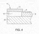
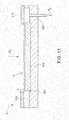
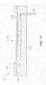
- the structure holder 11includes a top plate 13. As shown in Figures 3-4 , the top plate 13 is a ring. The top plate 13 may have other shapes and may extend entirely across the substrate 9 without limitation. The top plate 13 is adapted to contact the front surface of the structure 9 at the circumferential edge 5 of the structure.
- the structure holder 11includes a back plate 15 for contacting the back surface of the structure 9 adjacent the circumferential edge 5.
- the back plate 15includes a peripheral ring 20 that extends upward toward the top plate 13.
- the peripheral ring 20may be part of the top plate 13 or may be separate from both the top plate 13 and back plate 15.
- the back plate 15, top plate 13 and peripheral ring 20are both adapted to form a peripheral chamber 18 between the top plate 13, back plate 15 (including the peripheral ring) and circumferential edge 5 of the structure 9.
- the back plate 15 and top plate 13form a seal with the structure 9 which allows the pressure in the peripheral chamber 18 to be decreased relative to the pressure exterior to the holder 11 as described below.
- the peripheral chamber 18may be formed by positioning the semiconductor structure 9 on the back plate 15 and lowering the top plate 13 onto the back plate 15 until a seal is formed between the top plate 13, back plate 15 and circumferential edge 5 of the structure 9.
- the holder 11includes a vent 22 in the back plate 15 for adjusting the pressure in the peripheral chamber 18.
- the ventmay extend through the front plate 13 and/or peripheral ring 20.
- the vent 22may be in fluid communication with a pump (not shown) for decreasing the pressure in the peripheral chamber 18.
- the holder 11may be part of an apparatus 36 for distending a structure 9.
- the apparatus 36may also include a housing 35 which defines a main chamber 27 in which the holder 11 is mounted.
- the apparatus 36may include a vent 32 that is in fluid communication with a pump (not shown) for regulating the pressure P 1 in the main chamber.
- the vent 22 within the structure holder 11extends through the housing 35.
- a pressure P 1may be maintained in the main chamber 27 and a different pressure, P 2 , may be maintained in the peripheral chamber 18 of the structure holder 11.
- the structure 9may be distended (i.e., the radius of the substrate may be increased).
- P 1may be at least about 10 MPa greater than P 2 or, at least about 20 MPa, at least about 50 MPa or at least about 75 MPa greater than P 2 (e.g., from about 10 MPa to about 100 MPa, from about 10 MPa to about 50 MPa or from about 10 MPa to about 25 MPa).
- P 1is ambient pressure.
- the main chamber 27 and housing 35may be eliminated and the housing may be exposed to the ambient environment (i.e., atmospheric pressure).
- a heating element 30may be used to heat the structure 9 during distension to activate the dislocation source layer. As described above, the structure may be heated to a temperature of from about 650 °C to about 1000 °C or from about 700 °C to about 1000 °C.
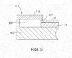
- the top plate 113includes a projection 117 for contacting the front surface 8 of the structure 9.
- the projection 117may form a seal with the structure 9 to allow the pressure in the peripheral chamber 118 to be increased or decreased.
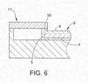
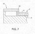
- the structure 9has a coating 39 ( Fig. 6 ) or coating 40 ( Fig. 7 ) on at least a portion of the structure surfaces.
- the coating 39extends over the circumferential edge 5 of the structure 9 and a portion of the front surface 8 and back surface 4 near the peripheral edge 5.
- the coating 40also extends over the entire back surface 4 of the structure.
- a coatingmay extend over one or more surfaces of the structure holder.
- the coating 39 or coating 40may be composed of a low-friction material such as graphite, hexagonal boron nitride, MS 2 , WS 2 , SiCN, AlCr(V)N, TiAl(Y)N, CaF 2 , BaF 2 , SrF 2 or BaCrO 4 .
- the structure 9has a coating on the front surface of the structure that reduces or even prevents evaporation of volatile film components of the structure. Suitable coatings for reducing evaporation include amorphous silicon.
- the top plate 213 of the structure holder 211includes a recess adapted for forming a central chamber 240 between the top plate 213 and the front surface 8 of the structure 9 during use of the structure holder 211.
- the central chamber 240is formed by lowering the top plate 213 onto the semiconductor structure 9.
- the recessis defined by an annular wall 242.
- the recesshas a radius that is less than the strained radius of the structure.
- strained radiusrefers to the radius of the structure prior to radial distension (deformation) of the structure 9 by use of the structure holder 211.
- the top plate 213includes a vent 246 that is in fluid communication with a pump (not shown) to maintain a pressure P 1 in the central chamber 240. In this manner a differential pressure may be maintained between the central chamber 240 and peripheral chamber 218 to cause the structure 9 to be radially distended. By maintaining the pressure P 1 in the central chamber 240 greater than pressure P 2 in the peripheral chamber 218, the structure may be distended. Pressures P 1 and/or P 2 may be within the ranges described above.
- FIG. 11An example of a self-limiting structure holder for radially distending the structure is shown in Figure 11 .
- the holder components shown in Figure 11 that are analogous to those of Figure 3are designated by the corresponding reference number of Figure 3 plus "300".
- the back plate 315 of the structure holder 311includes a recess that is defined by an annular wall 352 adapted to limit the expansion of the structure during distension of the structure.
- the radius of the recess of the back plate 315is greater than the strained radius of the structure.
- the radius of the structure 9increases until the structure contacts the annular wall 352.
- distension of the structure 9ceases.
- FIG. 12Another embodiment of a self-limiting structure holder for radially distending the structure 9 is shown in Figure 12 .
- the holder components shown in Figure 12 that are analogous to those of Figure 3are designated by the corresponding reference number of Figure 3 plus "400".
- the holder 411includes a perforated wall 455 in the peripheral chamber 418 that is adapted to limit the expansion of the structure during distension of the structure 9.
- the perforations formed in the wall 455allow pressure to equilibrate through the peripheral chamber 418.
- the peripheral wall 455limits the distension of the structure 9 during radial distension.
- FIG. 13Another embodiment of a self-limiting structure holder for radially distending the structure is shown in Figure 13 .
- the holder components shown in Figure 13 that are analogous to those of Figure 3are designated by the corresponding reference number of Figure 3 plus "500".
- the peripheral ring 520 of the back plate 515 of the structure holder 511extends relatively close to the relaxed structure before use. During distension, the structure 9 expands radially until the structure 9 contacts the peripheral ring 520 to limit the distension of the structure.
- a compression plate 659may be used to apply downward pressure P 1 of the structure.
- the holder components shown in Figure 10 that are analogous to those of Figure 3are designated by the corresponding reference number of Figure 3 plus "600".
- a pressure P 2is maintained in the peripheral chamber 618. P 2 is less than P 1 to maintain a differential pressure to distend the structure 9.
- P 1may be at least about 10 MPa greater than P 2 or, as in other embodiments, at least about 20 MPa, at least about 50 MPa or at least about 75 MPa greater than P 2 (e.g., from about 10 MPa to about 100 MPa, from about 10 MPa to about 50 MPa or from about 10 MPa to about 25 MPa).
- Forcemay be applied through the compression plate 659 to the structure 9 by any suitable method such as by use of hydraulics, pneumatics or electric drives.
- the self-limiting features described abovemay be used in combination with the compression plate 659.
- a structure holder for radially distending a structuremay be adapted to distend a plurality of structures concurrently as shown in Figure 14 .
- the holder components shown in Figure 14 that are analogous to those of Figure 3are designated by the corresponding reference number of Figure 3 plus "700".
- the holder 711includes a back plate 715 that is adapted to contact the structures 9a, 9b, 9c, 9d adjacent circumferential edges of the structures.
- the holder 711includes a top plate 713 that contacts the structures 9a, 9b, 9c, 9d adjacent circumferential edges of the structures.
- a peripheral chamber 718is formed between the back plate 715, top plate 713 and circumferential edges of the structures 9a, 9b, 9c, 9d.
- the top plate 713contains chambers 760 that extend to the front surface of the structures 9a, 9b, 9c, 9d to allow the structures to be exposed to the pressure P 1 in the main chamber (not shown).
- the peripheral chamber 718is maintained at pressure
- the structures 9a, 9b, 9c, 9dmay be radially distended.
- the difference between P 1 and P 2may be at least about 10 MPa and within any of the ranges described above.
- P 1may be atmospheric pressure and, the top plate 713 may be a continuous part that does not contain separate chambers 760.
- the substrate holder shown in Figure 14is described and shown as having only one back plate and one top plate, it should be understood that the holder may have a plurality of separate back or top plates that seal individual structures or groups of structures.
- the substrate holder 711 shown in Figure 14is capable of radially distending four structures, it should be noted that the holder may be arranged such that more or less structures may be concurrently distended without limitation.
- FIG. 15An example of a self-limiting structure holder for processing a plurality of structures is shown in Figure 15 .
- the holder components shown in Figure 15 that are analogous to those of Figure 3are designated by the corresponding reference number of Figure 3 plus "800".
- the back plate 815includes a number of recesses adapted for receiving the structures 9a, 9b, 9c, 9d.
- the recessesare defined by annular walls 852a, 852b, 852c, 852d.
- the annular walls 852a, 852b, 852c, 852dact to limit the radial distension of the structures 9a, 9b, 9c, 9d.
- an apparatus that grips the structuresuch as at the peripheral edge by use of clamps or other gripping elements
- an apparatus that grips the structuremay be used to relax the heterostructure such as in apparatus described below.
- distension of the structuremay be achieved by use of a structure holder that is radially movable relative to the structure.
- the structure holdermay be part of an apparatus for distending the structure.
- Such apparatusmay be similar to the apparatus 36 shown in Figure 8 in that the apparatus includes a housing 35 which defines a main chamber 27 in which the holder is mounted.
- the apparatusmay include a heating element 30 to heat the structure 9 during distension by use of any of the structures of Figures 16-21 to activate the dislocation source layer.
- the structure holder 1720may include a plurality of triangular-shaped segments 1785 that point inward to a central axis A of the holder. Each segment has at least one fluid passageway 1787 formed therein to pull a vacuum on the substrate. The segments 1785 may be mounted for movement outward from the central axis A causing the substrate to distend.
- the apparatus 911may be a clamp that includes a front plate 931 and a back plate 932 that exerts a holding force on the substrate 9.
- the top plate 931 and back plate 932are rings.
- the top plate 931may have other shapes and may extend entirely across the substrate 9 without limitation.
- the front plate 931 and back plate 932may be movable radially outward from the center of the apparatus by any mechanical methods including use of pneumatics, hydraulics, motors and the like. It should be noted that such mechanical methods may be used to move any of the front plate and/or back plates in the structure holders described below.
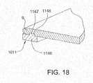
- the structure holder 1011includes a generally planar back plate 1146 that includes an annular boss 1147 that is sized and shaped to be received in a groove 1148 in the back of the structure 9.
- the boss 1147is movable such that it distends the structure 9.
- the structure holder 1220also includes a front plate 1250 having an annular ring 1252 that extends from the front plate.
- the ring 1252exerts a downward force on the structure 9 to prevent the structure from dislodging from the boss 1247 during distention of the structure during heating.
- Other structures for accomplishing this functionare contemplated within the scope of this disclosure.
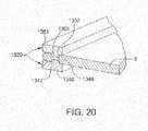
- the structure holder 1320includes a back plate 1346 and boss 1347 similar or identical to that shown in Figures 18 and 19 .
- the substrate holder 1320also includes a front plate 1351 and a front boss 1355 that is sized and shaped to be received in a groove 1357 in the front surface of the structure 9.
- a structure holder 1620includes a generally planar back plate 1681 and a flange 1683.
- the structure 9includes a ring 1680 attached to the back surface of the structure near the peripheral edge of the structure.
- the flange 1683is adapted to engage the ring 1680.
- the support 1681 and flange 1683are movable relative to the structure to distend the structure.
- the stress applied by the apparatus described aboveis cycled such as by reducing the differential pressure across the structure (e.g., by decreasing or increasing pressure in the peripheral or main chambers) or by reducing the stress applied in embodiments in which the apparatus grips the substrate. Such cycling may release any elastic stress formed in the structure.
- the terms “about,” “substantially,” “essentially” and “approximately” when used in conjunction with ranges of dimensions, concentrations, temperatures or other physical or chemical properties or characteristicsis meant to cover variations that may exist in the upper and/or lower limits of the ranges of the properties or characteristics, including, for example, variations resulting from rounding, measurement methodology or other statistical variation.
Landscapes
- Engineering & Computer Science (AREA)
- Physics & Mathematics (AREA)
- Condensed Matter Physics & Semiconductors (AREA)
- General Physics & Mathematics (AREA)
- Manufacturing & Machinery (AREA)
- Computer Hardware Design (AREA)
- Microelectronics & Electronic Packaging (AREA)
- Power Engineering (AREA)
- Chemical & Material Sciences (AREA)
- General Chemical & Material Sciences (AREA)
- Chemical Kinetics & Catalysis (AREA)
- Crystallography & Structural Chemistry (AREA)
- Materials Engineering (AREA)
- Metallurgy (AREA)
- Organic Chemistry (AREA)
- Recrystallisation Techniques (AREA)
- Container, Conveyance, Adherence, Positioning, Of Wafer (AREA)
- Crystals, And After-Treatments Of Crystals (AREA)
- Chemical Vapour Deposition (AREA)
- Semiconductor Lasers (AREA)
Description
- The present disclosure relates generally to preparation of semiconductor heterostructures with reduced strain and, in particular, to heterostructures with a semiconductor substrate that conforms to a surface layer having a different crystal lattice constant than the substrate, thereby forming a relatively low-defect heterostructure.
- Multi-layered structures comprising a device layer with a device quality surface and a substrate that has a different crystal lattice structure than the material of the device layer are useful for a number of different purposes. These multi-layered structures typically comprise multiple layers of material having differing lattice constants. The lattice mismatch between layers causes the layers to be strained. Misfit dislocations may spontaneously form in the device layer to relax the strain between layers. Such dislocations degrade the quality and usefulness of the multi-layer semiconductor structure.
- A continuing need exists for methods for relaxing the strain between lattice-mismatched semiconductor layers and for methods that result in substrates and device layers that are substantially free of dislocations.
- One aspect of the present disclosure is directed to a process for relaxing the strain in a heterostructure comprising a substrate, a surface layer disposed on the substrate and an interface between the substrate and the surface layer. The substrate comprises a central axis, a back surface which is generally perpendicular to the central axis, and a diameter extending across the substrate through the central axis. A dislocation source layer is formed in the substrate. The substrate is radially distended to generate dislocations and glide the dislocations from the dislocation source layer toward the surface layer.
- Another aspect of the present disclosure is directed to a process for preparing a relaxed heterostructure. A surface layer is deposited on a front surface of the semiconductor substrate thereby creating a strain between the surface layer and the substrate. A dislocation source layer is formed in the substrate. The strain in the surface layer and the substrate is relaxed by radially distending the substrate to generate dislocations and glide the dislocations from the dislocation source layer toward the surface layer.
- A further aspect of the present disclosure is directed to an apparatus for radially distending a semiconductor structure having a front surface, a back surface and a circumferential edge. The apparatus includes a structure holder comprising a top plate and a back plate for contacting the structure adjacent a circumferential edge of the structure. The top plate is adapted to contact the front surface of the structure and the back plate is adapted to contact the back surface of the structure. The top plate and back plate are further adapted to form a peripheral chamber between the top plate, back plate and circumferential edge of the structure.
- An additional aspect of the present disclosure is directed to an apparatus for radially distending a semiconductor structure having a front surface, a back surface, a circumferential edge and a central axis. The apparatus includes triangular-shaped segments that point inward to a central axis. The segments are configured for movement outward from the central axis to cause the structure to distend. Fluid passageways are formed in each segment for forming a vacuum between the segment and structure.
Figure 1 is a cross-sectional, schematic drawing of a silicon heterostructure;Figure 2 is a flow diagram depicting a process for preparing a heterostructure;Figures 3-4 are cross-sectional views of a semiconductor structure and a structure holder for distending the semiconductor structure;Figure 5 is a cross-sectional view of a semiconductor structure and another embodiment of a structure holder for distending the semiconductor structure;Figures 6-7 are cross-sectional views of a semiconductor structure having a coating thereon and the structure holder ofFigure 3 ;Figure 8 is a cross-sectional schematic view of a semiconductor structure and an apparatus for distending the structure with the structure holder ofFigure 3 mounted therein;Figure 9 is a cross-sectional view of a semiconductor structure and another embodiment of a structure holder for distending the semiconductor structure;Figure 10 is a cross-sectional view of a semiconductor structure and a structure holder having a compression plate for distending the semiconductor structure;Figure 11 is a cross-sectional view of a semiconductor structure and another example of a structure holder for distending the semiconductor structure;Figure 12 is a cross-sectional view of a semiconductor structure and another embodiment of a structure holder for distending the semiconductor structure;Figure 13 is a cross-sectional view of a semiconductor structure and a structure holder having a compression plate for distending the semiconductor structure;Figure 14 is a cross-sectional view of a plurality of semiconductor structures and a structure holder for distending the semiconductor structures;Figure 15 is a cross-sectional view of a plurality of semiconductor structures and other examples of a structure holder for distending the semiconductor structures;Figure 16 is a top view of another example of a structure holder for distending a semiconductor structure;Figure 17 is a cross-sectional view of a semiconductor structure and another example of a structure holder for distending the semiconductor structure;Figure 18 is a cross-sectional view of a semiconductor structure having a groove and another example of a structure holder for distending the semiconductor structure;Figure 19 is a cross-sectional view of a semiconductor structure and the structure holder ofFigure 18 with a top plate;Figure 20 is a cross-sectional view of a semiconductor structure having two grooves and another example of a structure holder for distending the semiconductor structure; andFigure 21 is a cross-sectional view of a semiconductor structure and another example of a structure holder having a flange.- Corresponding reference characters indicate corresponding parts throughout the drawings.
- In accordance with one or more aspects of the present disclosure, heterostructures with reduced strain between the substrate and a surface layer having a different lattice constant than the substrate may be prepared such as by the process of
Figure 2 . The surface layer may also be referred to herein as an "epitaxial layer", "heteroepitaxial layer", "deposited film", "film", "heterolayer" or "deposited layer". A heterostructure having a substantially relaxed surface layer and a reduced concentration of misfit dislocations, also referred to as threading dislocations, may be formed. - In general, the processes of the present disclosure may include forming a dislocation source layer in a semiconductor substrate, depositing a heterolayer on the substrate before or after formation of the dislocation source layer and radially distending the heterostructure to generate (i.e., "activate") dislocations and glide the dislocations from the dislocation source layer toward the surface layer. The activation of the source layer and the gliding of the dislocations from the source layer toward the interface with the deposited layer occur concurrently by applying a stress (e.g., tension) to the substrate. The stress may be applied in one or more steps and in various combinations to activate and glide the dislocations, thereby plastically stretching the heterostructure.
- The heterolayer may have a crystal lattice constant, aS1, which differs from the native crystal lattice constant of the substrate, aS to form a film on the surface of the substrate. Generally, the crystal lattice constant, aS1, of the heterolayer is greater than the native crystal lattice constant of the substrate, as, such that by controlling the generating and gliding of the dislocation loops in the substrate by distention, the substrate may be plastically deformed and aligned more suitably with the crystal lattice of the film thereby allowing the film to be completely relaxed and having a reduced density of threading dislocations on the substrate.
- The methods of the present disclosure have several advantages over conventional methods for relaxing heterolayers. Conventional methods create a large asymmetry in the stresses between the film and the substrate which leads to dislocation generation where the stresses are the greatest, i.e., the film. By confining the dislocation loops to the film, the dislocations leave segments behind which act as degrading threading dislocations. Much effort has been employed in attempting to minimize the density of such threading dislocations.
- Documents
US6189591 andUS5725728 describe a method and an apparatus for radially distending a semiconductor structure.Pizzagalli et al (Phys. Rev. B 79, 045203, 2009) present a theoretical study about pressure effects and dislocations properties in semiconductors. DocumentsUS2006091377 andDE19802977 are concerned with a method for relaxing strain in a heterostructure by gliding dislocations. - In contrast, methods of the present disclosure result in an asymmetry of stresses with the dislocation generation occurring in the substrate (e.g., by weakening the substrate and using a relatively thin film to void dislocation generation therein while weakening the substrate). This allows dislocations to be confined to the substrate while forming the misfit dislocation layer at the interface between the substrate and the film. Upon weakening the substrate by introducing dislocations in a variety of controlled ways, external stresses may be applied to the system to activate the dislocations. This differs from conventional methods which result in self-relaxation due to the relatively large intrinsic, internal stresses (i.e., relaxation without application of external stresses). The methods of the present disclosure involve relaxation other than by self-relaxation by weakening and application of external stress at appropriate temperatures with a relatively thin film such that self-relaxation does not occur.
- Referring to
Figure 1 , the semiconductor substrate 1 may be any single crystal semiconductor material suitable for use as a substrate for supporting a surface layer such as by deposition of an epitaxial layer by chemical vapor deposition. In general, the semiconductor substrate may be composed of a material selected from the group consisting of silicon, silicon carbide, sapphire, germanium, silicon germanium, gallium nitride, aluminum nitride, gallium arsenic, indium gallium arsenic or any combination thereof. Typically, the semiconductor substrate is composed of silicon. - The semiconductor substrate 1 may be in any shape suitable for both use as a substrate for depositing a surface layer and suitable for applying a stress to the substrate material as described in more detail below. Typically, the semiconductor substrate has a
central axis 2; aninterface 3 with the depositedlayer 7 and aback surface 4, the substrate-surface layer interface 3 andback surface 4 being generally perpendicular to thecentral axis 2; a thickness t, corresponding to the distance from the interface to the back surface of the substrate; acircumferential edge 5; and a diameter D, extending across the substrate through the central axis. It should be noted that, for illustrative purposes, theback surface 4 will be described as the opposing surface at or near which the dislocation source layer will be formed and as such may be referred to herein as the "opposing surface" and/or the "damaged surface." In this regard, the heterostructure itself and the depositedlayer 7 described below are generally concentric with the substrate 1 and also include acentral axis 2; acircumferential edge 5; and a diameter D, extending across the heterostructure (and also the surface layer) and through the central axis. - The substrate 1 may have any suitable diameter for use as a substrate upon which a semiconductor layer will be deposited. In general, the substrate 1 has diameter of about 150 mm or more. Typically, the substrate 1 has a diameter of about 200 mm or more, about 300 mm or more or even about 450 mm or more. It should be noted that the substrate diameter may be the diameter prior to plastically deforming the heterostructure, in which case, the diameter may increase from the stated values after plastic deformation as discussed in more detail below. Alternatively, the substrate prior to plastic deformation may have a diameter less than the stated values such that the diameter after plastic deformation is approximately equal to the stated values.
- Similarly, the substrate 1 may have any thickness, t, suitable for use as a substrate upon which a semiconductor layer may be deposited. For example, the substrate may have a thickness, t, of from about 500 microns to about 1000 microns, typically from about 600 microns to about 1000 microns, from about 700 microns to about 1000 microns, from about 700 microns to about 900 microns or even from about 700 microns to about 800 microns.
- The substrate 1 may be a single crystal silicon wafer that has been sliced from a single crystal silicon ingot grown by Czochralski crystal growing methods having a diameter of about 150 mm or more, about 200 mm or more, about 300 mm or more or even about 450 mm or more and a thickness of from about 675 microns to about 1000 microns or even from about 725 microns to about 925 microns.
- The substrate surface upon which the epitaxial layer is deposited may be polished such that it is suitable for depositing the epitaxial layer or may be further conditioned prior to chemical vapor deposition. The opposing surface may also be polished or alternatively may be un-polished, i.e., as-ground, as-lapped or as-lapped and etched, without departing from the scope of the present disclosure. In various examples, the opposing surface may be left in an unpolished state, wherein the as-ground, as-lapped or as-lapped and etched surface may be utilized as a dislocation source layer. Alternatively or in addition, the opposing surface may be damaged to form a dislocation source layer as described in more detail below.
- It should be noted that Czochralski-grown silicon typically has an oxygen concentration within the range of about 5 x 10¹⁷ to about 9 x 10¹⁷ atoms/cm3 (ASTM standard F-121-83). In general, a single crystal silicon wafer used for a substrate in the present disclosure may have an oxygen concentration falling anywhere within or even outside the range typically attainable by the Czochralski process, provided the oxygen concentration is not so excessive as to prevent the activation and gliding of the dislocations.
- A
surface layer 7 may be located on the front surface of the substrate 1. The depositedlayer 7 may be any single crystal semiconductor material suitable for depositing as an epitaxial layer by chemical vapor deposition. Generally, the heterolayer includes a crystal lattice constant, aS1, that is greater than the native crystal lattice constant of the substrate, as. The deposited layer may be composed of any suitable material such as a material selected from the group consisting of silicon, silicon carbide, sapphire, germanium, silicon germanium, gallium nitride, aluminum nitride, gallium arsenide, indium gallium arsenide or any combination thereof. When the substrate is composed of silicon, heterolayers with a greater lattice constant include, for example, germanium, silicon germanium, polytypes of silicon carbide, gallium arsenide and indium gallium arsenide. - In one example, the deposited layer is silicon germanium, also referred to herein as SiGe. The specific composition of the deposited SiGe layer may vary without departing from the scope of the present disclosure. Typically, the SiGe layer comprises at least about 10% Ge, and in some instances may comprise about 15%, about 20%, about 25%, about 35%, about 50% Ge or more (e.g., 60%, 70%, 80%, 90% or more). In one preferred embodiment, however, the SiGe layer has a Ge concentration in the range of at least about 10% to less than about 50%, or from at least about 15% to less than about 35%, with a concentration of about 20% Ge being preferred.
- Essentially any technique generally known in the art may be used to form the deposited layer (e.g., SiGe layer), such as one of the known epitaxial deposition techniques. Generally speaking, the thickness of the deposited layer may vary greatly without departing from the scope of the present disclosure. The thickness may have, for example, a substantially uniform thickness, the average thickness thereof being at least about 0.1 microns, at least about 0.5 microns, at least about 1.0 micron, and even at least about 2.0 microns. Alternatively, it may be desirable to express thickness in terms of a range. For example, the average thickness may typically be in the range of from about 0.1 microns to about 2.0 microns, such as from about 0.5 micron to about 1.0 micron.
- It should be noted that as the deposited layer is grown on a substrate having a differing lattice constant, an equal, but opposite stress is formed in both the deposited layer and the substrate. The relative amount of stress in the deposited layer and the substrate, just above and just below the interface, is proportional to the relative thicknesses of the deposited layer and the substrate. As a result, the stress in the deposited layer just above the interface may be several orders of magnitude larger than the stress in the substrate just below the interface. For example, if a 500 nm SiGe layer comprising about 22% Ge is grown on a 700 micron thick silicon semiconductor substrate, the SiGe just above the interface will be under approximately 1.7 GPa of compression and the silicon just below the interface will be under only 5 MPa of tension. The stress in the deposited layer can increase during growth until the layer self-relaxes by forming misfit or threading dislocations in the deposited layer. To avoid self-relaxation of the deposited layer, therefore, it is preferable at least initially to grow a thin deposited layer on the substrate. Typically, the deposited layer will be grown to a thickness of from about 1 nm to about 100 nm, more typically from about 1 nm to about 50 nm, still more typically from about 10 nm to about 20 nm in the case of a SiGe layer being deposited on a single crystal silicon substrate. The thin layer may then be relaxed or partially relaxed to at or near its native lattice constant by activating and expanding dislocations in the substrate as discussed in more detail below. If a thicker deposited layer is desired, additional material may be deposited after the layer has been sufficiently relaxed.
- Essentially any technique generally known in the art may be used to form a deposited layer on the substrate. For example, epitaxial deposition techniques (e.g., atmospheric-pressure chemical vapor phase deposition (APCVD); low- or reduced-pressure CVD (LPCVD); ultra-high-vacuum CVD (UHVCVD); molecular beam epitaxy (MBE); or, atomic layer deposition (ALD)) may be used wherein, for example, SiGe material is deposited. The epitaxial growth system may comprise a single-wafer or a multiple-wafer batch reactor.
- The
surface layer 7 includes a surface which forms thefront surface 8 of the heterostructure. Thesurface layer 7 may continuously extend across the entire diameter of the substrate 1 as shown inFigure 1 . In some examples, thesurface layer 7 does not extend continuously over the substrate 1 but rather includes a number of discontinuous segments or "islands" of semiconductor material that are disposed on the substrate as further described below. For example, the surface layer may be disposed over less than about 95% of the substrate or, less than about 80%, less than about 60%, less than about 40% or less than about 20% of the substrate. - A
dislocation source layer 6 is located within the substrate 1 and may be spaced from the substrate surface upon which the epitaxial layer is to be deposited. Typically, thedislocation source layer 6 is at or near the surface opposing the surface upon which the epitaxial layer has been or will be deposited. For example, if the epitaxial layer is to be deposited on the front surface of the substrate, thedislocation source layer 6 will be at or near theback surface 4 of the substrate. In such an example, the front surface of the substrate will become the interface between the substrate and the depositedlayer 7. - The
source layer 6 is present or is installed over a substantial radial width of the substrate 1. In the embodiment illustrated inFigure 1 , thesource layer 6 extends across the entire diameter of the substrate 1. Although this embodiment is preferred, in other embodiments the source layer may not extend over the entire diameter. In general, therefore,source layer 6 will have a radial width of typically at least about 75%, more typically at least about 85% and still more typically at least about 95% of the radius of the wafer or even at least about 99% of the radius of the wafer. In some embodiments, thesource layer 6 extends to within a few millimeters of the circumferential edge, for example, to within about 1 mm of the circumferential edge. - In general, the
source layer 6 may include any portion of the substrate provided the source layer does not include the surface upon which the epitaxial layer is to be deposited. Generally thesource layer 6 has a thickness of about 100 microns or less, about 50 microns or less, about 25 microns or less or about 10 microns or less (e.g., from about 1 micron to about 100 microns, from about 1 micron to about 50 microns, from about 1 micron to about 25 microns or from about 5 microns to about 25 microns). Thesource layer 6 may include the back surface of the substrate and extend therefrom. It should be noted that thesource layer 6 need not include the back surface of the wafer and may extend from a depth from the back surface toward the front surface of the substrate. - The
dislocation source layer 6 may be any layer capable of generating a measurable concentration of dislocations when subjected to sufficiently high stresses at sufficiently high temperatures. In general, thedislocation source layer 6 is capable of generating a measurable concentration of dislocations when subjected to tension of between about 5 MPa and about 100 MPa (typically at around about 15 MPa at temperatures of between about 500°C and about 1000°C) as discussed in more detail below with regard to the activation of dislocations within the substrate. - The
dislocation source layer 6 may be formed in the substrate 1 before or subsequent to the deposition of thesurface layer 7. When the substrate is a wafer sliced from a single crystal ingot, thedislocation source layer 6 may be mechanical damage caused by the slicing process, grinding process or lapping process included as part of the overall wafering process. - Alternatively or in addition, the
dislocation source layer 6 may be formed in part or in its entirety by mechanically damaging the back surface of the substrate by one or more processes selected from the group consisting of: grinding the back surface, lapping the back surface, installing soft damage by sandblasting the back surface, forming indentations on the back surface, implanting ions in the back surface and/or combinations thereof. - The
dislocation source layer 6 may be formed by pressing an array of pointed pins onto the wafer back surface to form indentations in the back surface. The indentations may be formed non-uniformly across the surface or may be formed in a predetermined pattern. Such a pattern may be arranged in a specific relation to the wafer crystal directions. For example, a square matrix pattern could be arranged at a shallow angle to the 110 direction. This may allow for the dislocations generated at these sites to glide along parallel glide planes and not interact with each other. Furthermore, accurate control of the dislocation loop density may be had by such a treatment. - The
source layer 6 may be formed by implanting ions through the back surface of the substrate. The implanted ions may be electrically isoelectronic, neutral, or inert to minimize any effect upon the electronic properties of the substrate. For example, the implanted ions may be selected from the group consisting of silicon, germanium, hydrogen, helium, neon, argon, xenon, and combinations thereof. - The ions are implanted to a target depth, Di, relative to the back surface. As a practical matter, however, some of the implanted ions will not travel this distance and others will travel an even greater distance (i.e., reach a greater depth relative to the back surface). The actual ion implantation depth may vary from Di by about 5%, 10%, 15%, 20%, 25%, or more. This creates a zone or layer of amorphous material containing a relatively high concentration of implanted ions at or near Di, with the concentration of implanted ions decreasing from Di in the direction of
front surface 3 and in the opposite direction. Target depth, Di, may also be referred to as the projected range of the implanted ions. - Implantation depth may be affected, at least in part, by the ionic species implanted, since lighter ions tend to penetrate further into the substrate for a given implantation energy. Thus, for example, at an implant energy of 50 keV, silicon ions will have an average implant depth of about 750 Å, whereas germanium ions will have an average implant depth of 400 Å. In general, ions are preferably implanted at an energy of at least about 30 keV, such as at least about 40 keV, or even at least about 50 keV. In one application, ions are implanted at an energy of at least about 45 keV and less than about 55 keV. The ion and the implant energy selected should be sufficient to form an amorphous layer in the substrate which acts as the dislocation source layer.
- Generally, dislocation loops form at the end of range of the implanted ions upon subsequent anneal if sufficient energy is used to implant a sufficient concentration of ions to form an amorphous layer of silicon. Typically, the dislocation loops may form at a depth of about 100 Å to about 300 Å below the implanted ions, although the exact depth may be more or less. In general, it is more difficult to form amorphous material using lower mass elements. Accordingly, a much higher concentration of low mass elements must be used to induce sufficient damage, whereas lower concentrations of high mass elements are sufficient to form amorphous silicon. For example, when the implanted ions are silicon ions, the implanted dose is preferably at least about 2 x 10¹⁴ atoms/cm2, such as at least about 5 x 10¹⁴ atoms/cm2, or even at least about 1 x 10¹⁵ atoms/cm2. In one example, the implanted ion dose is at least about 2 x 10¹⁵ atoms/cm2. By comparison, when the implanted ions are the higher mass germanium ions, the implanted dose is preferably at least about 6 x 10¹³ atoms/cm2, such as at least about 1 x 10¹⁴ atoms/cm2, or even at least about 5 x 10¹⁴ atoms/cm2. In one example, the implanted ion dose is at least about 1 x 10¹⁵ atoms/cm2.
- In some examples, the
source layer 6 is formed by grinding the back surface of the substrate. The surface may be ground using any grinding processes typically used in the semiconductor silicon industry to shape the surface of a silicon wafer after being sliced from a Czochralski-grown single crystal silicon ingot. In an example, the back surface may be ground using a grinding process which uses a grit size of about 600. - The dislocation source layer may be activated to form dislocations at or near the source layer which may be glided toward the substrate-surface layer interface. In accordance with embodiments of the present disclosure, activation and gliding of dislocations is performed after the surface layer has been deposited on the substrate such that the substrate and/or surface layer are under strain.
- The dislocation source layer is activated by subjecting the dislocation source layer (and typically subjecting the substrate) to a stress by distending (which may be also be referred to herein as "stretching," "tension" or "tensile stress") the substrate at an elevated temperature to cause the formation of dislocations. Distension is applied to the entire substrate in a direction perpendicular to the axis, i.e., in the radial direction using one or more suitable apparatus. That is, the wafer is stretched radially outward from the peripheral edge. In this manner, the dislocations will form at or near the source layer and the dislocations will glide towards the opposite surface.
- In general, more heavily damaged dislocation source layers will activate at lower stress levels and at lower temperatures whereas less heavily damaged dislocation source layers will activate at higher stress levels and temperatures. In general, stress applied by tension of at least about 5 MPa, typically from about 5 MPa to about 100 MPa or from about 10 MPa to about 100 MPa is applied to the dislocation source layer at a temperature of between about 550°C and about 1000°C. More typically, the tension is from about 10 MPa to about 50 MPa or from about 10 MPa to about 25 MPa. Typically, the activation and/or gliding of the dislocations is carried out at temperatures from about 650°C to about 1000°C or even from about 700°C to about 1000°C. For example, typical stresses that may be applied to activate a dislocation source layer formed by lapping and/or grinding may be about 15 MPa at temperatures greater than about 600°C and even more typically at temperatures greater than about 700°C. Other, more highly damaged layers may activate at even lower stress levels.
- The substrate is maintained under tension at an elevated temperature for duration sufficient to activate and glide dislocations. In general, the substrate is maintained under tension and at an elevated temperature, as described above, for a period of at least about 10 seconds and may be maintained under those conditions for a period of at least about 5 hours, at least about 10 hours or even longer. Typically, the substrate is maintained under tension at an elevated temperature for a period of at least about 1 minute, from about 5 minutes to about 60 minutes, more typically from about 10 minutes to about 45 minutes and may be from about 10 minutes to about 20 minutes. It should be noted that the higher tension levels and higher temperatures each tend to reduce the duration required to activate and glide the dislocations.
- Distension may be applied to the substrate alone or, may be applied to the entire heterostructure (i.e., both the substrate and heterolayer). Further, it is preferred that the stress applied by distention be relatively uniform (in direction and/or magnitude) throughout the heterostructure (e.g., both radially and circumferentially). It should be noted that the degree of uniformity of stress may be limited by the apparatus used to distend the substrate and some variation (radial or circumferential variation) may result from uneven distribution of stress. At least about 5 MPa of stress is applied along the entire circumference of the substrate or, at least about 10 MPa of stress is applied along the entire circumference of the substrate.
- Upon application of sufficient stress, dislocations continually form at the dislocation source layer and glide toward the substrate-surface layer interface. At a given point of time during application of stress, the dislocations may generally be uniformly distributed throughout the thickness of the substrate. Upon reaching the substrate-surface layer interface, the dislocations form misfit interfacial dislocations at the interface. The misfit dislocations increase in density at the interface during distension of the substrate and continue to relax the strain between the surface layer and the substrate. The strain is eventually balanced upon a build-up of sufficient density of misfits.
- The dislocations that are generated from the dislocation source layer and which glide toward the substrate-surface layer interface may be substantially parallel to the back and front surfaces of the heterostructure (i.e., are arranged laterally). It is believed that a relatively small amount or even no threading dislocations are generated from the dislocation source layer.
- It is preferred that the distension of the substrate cease at or near the point at which the strain is balanced as further generation and gliding of dislocations may cause dislocations to penetrate the surface layer. Once distension of the substrate is stopped, the dislocations in transit in the substrate cease to glide to the interface and no further dislocations are generated (i.e., dislocations become frozen-in).
- The number of dislocations that may be present in the substrate at any given point of application of stress and heat may be at least about 1x10⁵ dislocations/cm2 or even at least about 5x10⁵ dislocations/cm2 (e.g., from about 1x10⁵ dislocations/cm2 to about 5x10⁷ dislocations/cm2 or from about 5x10⁵ dislocations/cm2 to about 1x10⁷ dislocations/cm2). The number density of the dislocations may be determined using any dislocation loop detection method including, for example, sampling the substrate and subjecting the sample to a delineating etchant prior to viewing and counting the dislocation loops through a microscope.
- In some examples, the stress applied to the substrate by distension of the substrate is reduced to a value less than a threshold value at which dislocations are generated from the dislocation source layer but at a sufficient magnitude to allow the existing dislocations to glide further upwards toward the interface. In this manner, a heterostructure having a substrate substantially free of dislocations may be produced. An initial stress S1 may be applied to the substrate by distension of the substrate to generate and glide dislocations from the source layer to the substrate-surface layer interface. The applied stress is then lowered to S2 (i.e., S2 is less than S1). The stress S2 is a stress less than a threshold value at which dislocations are generated from the dislocation source layer and which allows the existing dislocations to glide further upwards toward the interface to produce a substrate substantially free of dislocations. S1 may be at least about 5 MPa, at least about 10 MPa or at least about 25 MPa (e.g., from about 5 MPa to about 100 MPa or from about 10 MPa to about 100 MPa). S2 may be less than about 10 MPa, less than about 5 MPa or even less than about 1 MPa. Typically, even at stresses on the order of about 1 MPa, the dislocations will glide at a velocity of about 1 micron per second at a temperature of about 850°C or about 2.5 microns per second at a temperature of about 900°C.
- The magnitude of stress, the time of application of stress and/or the temperature at which stress is applied to the substrate may be varied depending on the difference between the lattice constant, aS, of the substrate and the lattice constant, aSL, of the semiconductor material of the surface layer. Depending on the substrate material chosen and the semiconductor material deposited thereon, aSL and as may vary. In general, distension is effective to relax the heterolayer when aSL is greater than as, i.e., when the ratio aSL/aS is greater than 1. The ratio aSL/aS may be from about 1.01 to about 1.16 or, from about 1.01 to about 1.10, from about 1.01 to about 1.08, from about 1.01 to about 1.05, from about 1.02 to about 1.16 or from about 1.05 to about 1.16.
- By gliding the dislocations to the interface, the surface layer may be at least about 85% relaxed, at least about 90% relaxed, at least about 95% relaxed or even completely relaxed, i.e., 100% relaxed. The surface layer may be substantially free of threading dislocations or may have a concentration of threading dislocations of less than about 104 threading dislocations/cm2.
- In examples in which the surface layer is not continuous but includes discontinuous segments (i.e., islands) disposed on the surface of the substrate, the discontinuous segments become relaxed by generating and gliding dislocations from the dislocation source layer to the interface with the islands to create misfit interfacial dislocations between each island and the substrate. Dislocations which reach the surface of the substrate between islands dissipate at the surface which allows the area between islands to be substantially free of dislocations upon completion of distension. After relaxation of the islands, semiconductor material may be further deposited to produce a surface layer that continuously extends over the entire diameter of the substrate. In such examples, the dislocations below the islands propagate laterally at the interface between the newly deposited material and the substrate thereby relaxing the newly deposited material and the continuous surface layer as a whole.
- The relaxed heterostructure fabricated by any of the methods described above may be used to fabricate silicon-on-insulator structures for integrated circuits using wafer bonding and layer transfer methods, or to subsequently fabricate strained silicon-on-insulator structures.
- Additional layers may be deposited on the relaxed surface layer thereby forming heteroepitaxial structures having a strained layer on top of the relaxed layer on top of a substrate. Such a structure may also be used to transfer both the relaxed layer and strained layer to another substrate, thereby forming a heteroepitaxial structure having a buried strained layer or alternatively a buried strained layer on insulator. That is, the heteroepitaxial structure may have a relaxed layer of semiconductor material on top of a strained layer of semiconductor material on top of either a substrate or an insulating layer on a substrate.
- In addition, the structures fabricated by the methods of the present disclosure may be used to fabricate semiconductor devices such as field effect transistor (FET) or modulation-doped field effect transistor (MODFET) layer structures. Relaxed SiGe layers can also be used for a variety of other applications, such as thermoelectric cooling devices.
- In this regard, the processes described herein relating to distension of the substrate may be performed with use of any of the apparatus described below.
- Referring now to
Figures 3-15 , distension of the substrate may be achieved by use of a substrate holder that includes chambers and/or fluid passageways for applying a differential pressure across the substrate. - Referring now to
Figures 3-4 , distension of thestructure 9 is achieved by use ofstructure holder 11. Thestructure holder 11 includes atop plate 13. As shown inFigures 3-4 , thetop plate 13 is a ring. Thetop plate 13 may have other shapes and may extend entirely across thesubstrate 9 without limitation. Thetop plate 13 is adapted to contact the front surface of thestructure 9 at thecircumferential edge 5 of the structure. - The
structure holder 11 includes aback plate 15 for contacting the back surface of thestructure 9 adjacent thecircumferential edge 5. Theback plate 15 includes aperipheral ring 20 that extends upward toward thetop plate 13. However, in other embodiments, theperipheral ring 20 may be part of thetop plate 13 or may be separate from both thetop plate 13 and backplate 15. Theback plate 15,top plate 13 andperipheral ring 20 are both adapted to form aperipheral chamber 18 between thetop plate 13, back plate 15 (including the peripheral ring) andcircumferential edge 5 of thestructure 9. Generally, theback plate 15 andtop plate 13 form a seal with thestructure 9 which allows the pressure in theperipheral chamber 18 to be decreased relative to the pressure exterior to theholder 11 as described below. Theperipheral chamber 18 may be formed by positioning thesemiconductor structure 9 on theback plate 15 and lowering thetop plate 13 onto theback plate 15 until a seal is formed between thetop plate 13, backplate 15 andcircumferential edge 5 of thestructure 9. - The
holder 11 includes avent 22 in theback plate 15 for adjusting the pressure in theperipheral chamber 18. Alternatively, the vent may extend through thefront plate 13 and/orperipheral ring 20. Thevent 22 may be in fluid communication with a pump (not shown) for decreasing the pressure in theperipheral chamber 18. - Referring now to
Figure 8 , theholder 11 may be part of anapparatus 36 for distending astructure 9. Theapparatus 36 may also include ahousing 35 which defines amain chamber 27 in which theholder 11 is mounted. Theapparatus 36 may include avent 32 that is in fluid communication with a pump (not shown) for regulating the pressure P1 in the main chamber. Thevent 22 within thestructure holder 11 extends through thehousing 35. In this manner, a pressure P1 may be maintained in themain chamber 27 and a different pressure, P2, may be maintained in theperipheral chamber 18 of thestructure holder 11. By maintaining the pressure P1 in themain chamber 27 greater than the pressure P2 in theperipheral chamber 18, thestructure 9 may be distended (i.e., the radius of the substrate may be increased). - In this regard, the arrows associated with pressures P1 and/or P2 in
Figures 3-15 are provided for exemplification purposes and should not be considered to limit the apparatus to a particular pressure profile (i.e., use of a vacuum or pressure in the peripheral chamber or main chamber). - During distension of the
structure 9, P1 may be at least about 10 MPa greater than P2 or, at least about 20 MPa, at least about 50 MPa or at least about 75 MPa greater than P2 (e.g., from about 10 MPa to about 100 MPa, from about 10 MPa to about 50 MPa or from about 10 MPa to about 25 MPa). In some examples, P1 is ambient pressure. In such examples, themain chamber 27 andhousing 35 may be eliminated and the housing may be exposed to the ambient environment (i.e., atmospheric pressure). - A
heating element 30 may be used to heat thestructure 9 during distension to activate the dislocation source layer. As described above, the structure may be heated to a temperature of from about 650 °C to about 1000 °C or from about 700 °C to about 1000 °C. - Another example of the
structure holder 111 is shown inFigure 5 . It should be noted that the holder components shown inFigure 5 that are analogous to those ofFigure 3 are designated by the corresponding reference number ofFigure 3 plus "100" (e.g.,part 15 becomes part 115). As shown inFigure 5 , thetop plate 113 includes aprojection 117 for contacting thefront surface 8 of thestructure 9. Theprojection 117 may form a seal with thestructure 9 to allow the pressure in theperipheral chamber 118 to be increased or decreased. - In some examples and as shown in
Figures 6-7 , thestructure 9 has a coating 39 (Fig. 6 ) or coating 40 (Fig. 7 ) on at least a portion of the structure surfaces. As shown inFigure 6 , thecoating 39 extends over thecircumferential edge 5 of thestructure 9 and a portion of thefront surface 8 andback surface 4 near theperipheral edge 5. As shown inFigure 7 , thecoating 40 also extends over theentire back surface 4 of the structure. Alternatively or in addition, a coating may extend over one or more surfaces of the structure holder. Thecoating 39 or coating 40 (or coatings which may extend over the structure holder) may be composed of a low-friction material such as graphite, hexagonal boron nitride, MS2, WS2, SiCN, AlCr(V)N, TiAl(Y)N, CaF2, BaF2, SrF2 or BaCrO4. In some embodiments, thestructure 9 has a coating on the front surface of the structure that reduces or even prevents evaporation of volatile film components of the structure. Suitable coatings for reducing evaporation include amorphous silicon. - Another embodiment of the
structure holder 211 is shown inFigure 9 . It should be noted that the holder components shown inFigure 9 that are analogous to those ofFigure 3 are designated by the corresponding reference number ofFigure 3 plus "200" (e.g.,part 15 becomes part 215). Thetop plate 213 of thestructure holder 211 includes a recess adapted for forming acentral chamber 240 between thetop plate 213 and thefront surface 8 of thestructure 9 during use of thestructure holder 211. Thecentral chamber 240 is formed by lowering thetop plate 213 onto thesemiconductor structure 9. The recess is defined by anannular wall 242. The recess has a radius that is less than the strained radius of the structure. As used herein, "strained radius" refers to the radius of the structure prior to radial distension (deformation) of thestructure 9 by use of thestructure holder 211. - The
top plate 213 includes avent 246 that is in fluid communication with a pump (not shown) to maintain a pressure P1 in thecentral chamber 240. In this manner a differential pressure may be maintained between thecentral chamber 240 andperipheral chamber 218 to cause thestructure 9 to be radially distended. By maintaining the pressure P1 in thecentral chamber 240 greater than pressure P2 in theperipheral chamber 218, the structure may be distended. Pressures P1 and/or P2 may be within the ranges described above. - An example of a self-limiting structure holder for radially distending the structure is shown in
Figure 11 . The holder components shown inFigure 11 that are analogous to those ofFigure 3 are designated by the corresponding reference number ofFigure 3 plus "300". Theback plate 315 of thestructure holder 311 includes a recess that is defined by anannular wall 352 adapted to limit the expansion of the structure during distension of the structure. The radius of the recess of theback plate 315 is greater than the strained radius of the structure. During distension, the radius of thestructure 9 increases until the structure contacts theannular wall 352. Upon contacting theannular wall 352, distension of thestructure 9 ceases. - Another embodiment of a self-limiting structure holder for radially distending the
structure 9 is shown inFigure 12 . The holder components shown inFigure 12 that are analogous to those ofFigure 3 are designated by the corresponding reference number ofFigure 3 plus "400". Theholder 411 includes aperforated wall 455 in theperipheral chamber 418 that is adapted to limit the expansion of the structure during distension of thestructure 9. The perforations formed in thewall 455 allow pressure to equilibrate through theperipheral chamber 418. Theperipheral wall 455 limits the distension of thestructure 9 during radial distension. - Another embodiment of a self-limiting structure holder for radially distending the structure is shown in
Figure 13 . The holder components shown inFigure 13 that are analogous to those ofFigure 3 are designated by the corresponding reference number ofFigure 3 plus "500". Theperipheral ring 520 of theback plate 515 of thestructure holder 511 extends relatively close to the relaxed structure before use. During distension, thestructure 9 expands radially until thestructure 9 contacts theperipheral ring 520 to limit the distension of the structure. - To distend (i.e., stretch) the
structure 9, alternatively or in addition to use of a higher pressure in the main chamber, a compression plate 659 (Fig. 10 ) may be used to apply downward pressure P1 of the structure. The holder components shown inFigure 10 that are analogous to those ofFigure 3 are designated by the corresponding reference number ofFigure 3 plus "600". A pressure P2 is maintained in theperipheral chamber 618. P2 is less than P1 to maintain a differential pressure to distend thestructure 9. As described above, P1 may be at least about 10 MPa greater than P2 or, as in other embodiments, at least about 20 MPa, at least about 50 MPa or at least about 75 MPa greater than P2 (e.g., from about 10 MPa to about 100 MPa, from about 10 MPa to about 50 MPa or from about 10 MPa to about 25 MPa). Force may be applied through thecompression plate 659 to thestructure 9 by any suitable method such as by use of hydraulics, pneumatics or electric drives. The self-limiting features described above may be used in combination with thecompression plate 659. - A structure holder for radially distending a structure may be adapted to distend a plurality of structures concurrently as shown in
Figure 14 . The holder components shown inFigure 14 that are analogous to those ofFigure 3 are designated by the corresponding reference number ofFigure 3 plus "700". Theholder 711 includes aback plate 715 that is adapted to contact thestructures holder 711 includes atop plate 713 that contacts thestructures peripheral chamber 718 is formed between theback plate 715,top plate 713 and circumferential edges of thestructures top plate 713 containschambers 760 that extend to the front surface of thestructures peripheral chamber 718 is maintained at pressure P2. - By maintaining P1 greater than P2, the
structures top plate 713 may be a continuous part that does not containseparate chambers 760. While the substrate holder shown inFigure 14 is described and shown as having only one back plate and one top plate, it should be understood that the holder may have a plurality of separate back or top plates that seal individual structures or groups of structures. Further, while thesubstrate holder 711 shown inFigure 14 is capable of radially distending four structures, it should be noted that the holder may be arranged such that more or less structures may be concurrently distended without limitation. - An example of a self-limiting structure holder for processing a plurality of structures is shown in
Figure 15 . The holder components shown inFigure 15 that are analogous to those ofFigure 3 are designated by the corresponding reference number ofFigure 3 plus "800". Theback plate 815 includes a number of recesses adapted for receiving thestructures annular walls annular walls structures - In addition to the apparatus described above, an apparatus that grips the structure (such as at the peripheral edge by use of clamps or other gripping elements) and allows the structure to be distended (stretched) may be used to relax the heterostructure such as in apparatus described below. Referring now to
Figures 16-21 , distension of the structure may be achieved by use of a structure holder that is radially movable relative to the structure. In such examples, the structure holder may be part of an apparatus for distending the structure. Such apparatus may be similar to theapparatus 36 shown inFigure 8 in that the apparatus includes ahousing 35 which defines amain chamber 27 in which the holder is mounted. The apparatus may include aheating element 30 to heat thestructure 9 during distension by use of any of the structures ofFigures 16-21 to activate the dislocation source layer. - Referring now to
Figure 16 , thestructure holder 1720 may include a plurality of triangular-shapedsegments 1785 that point inward to a central axis A of the holder. Each segment has at least onefluid passageway 1787 formed therein to pull a vacuum on the substrate. Thesegments 1785 may be mounted for movement outward from the central axis A causing the substrate to distend. - Referring now to
Figure 17 , theapparatus 911 may be a clamp that includes afront plate 931 and aback plate 932 that exerts a holding force on thesubstrate 9. As shown inFigure 17 , thetop plate 931 andback plate 932 are rings. Thetop plate 931 may have other shapes and may extend entirely across thesubstrate 9 without limitation. Thefront plate 931 andback plate 932 may be movable radially outward from the center of the apparatus by any mechanical methods including use of pneumatics, hydraulics, motors and the like. It should be noted that such mechanical methods may be used to move any of the front plate and/or back plates in the structure holders described below. - Referring now to
Figure 18 , in another example, thestructure holder 1011 includes a generallyplanar back plate 1146 that includes anannular boss 1147 that is sized and shaped to be received in agroove 1148 in the back of thestructure 9. Theboss 1147 is movable such that it distends thestructure 9. - In some examples and as shown in
Figure 19 , thestructure holder 1220 also includes afront plate 1250 having anannular ring 1252 that extends from the front plate. Thering 1252 exerts a downward force on thestructure 9 to prevent the structure from dislodging from theboss 1247 during distention of the structure during heating. Other structures for accomplishing this function are contemplated within the scope of this disclosure. - In other examples and as shown in
Figure 20 , thestructure holder 1320 includes aback plate 1346 andboss 1347 similar or identical to that shown inFigures 18 and19 . Thesubstrate holder 1320 also includes afront plate 1351 and afront boss 1355 that is sized and shaped to be received in agroove 1357 in the front surface of thestructure 9. - Referring to
Figure 21 , astructure holder 1620 includes a generallyplanar back plate 1681 and aflange 1683. Thestructure 9 includes aring 1680 attached to the back surface of the structure near the peripheral edge of the structure. Theflange 1683 is adapted to engage thering 1680. Thesupport 1681 andflange 1683 are movable relative to the structure to distend the structure. - In some examples, the stress applied by the apparatus described above is cycled such as by reducing the differential pressure across the structure (e.g., by decreasing or increasing pressure in the peripheral or main chambers) or by reducing the stress applied in embodiments in which the apparatus grips the substrate. Such cycling may release any elastic stress formed in the structure.
- As used herein, the terms "about," "substantially," "essentially" and "approximately" when used in conjunction with ranges of dimensions, concentrations, temperatures or other physical or chemical properties or characteristics is meant to cover variations that may exist in the upper and/or lower limits of the ranges of the properties or characteristics, including, for example, variations resulting from rounding, measurement methodology or other statistical variation.
- When introducing elements of the present disclosure or the preferred embodiments(s) thereof, the articles "a", "an", "the" and "said" are intended to mean that there are one or more of the elements. The terms "comprising", "including" and "having" are intended to be inclusive and mean that there may be additional elements other than the listed elements.
Claims (14)
- An apparatus for radially distending a semiconductor structure having a front surface, a back surface and a circumferential edge (5), the apparatus comprising:
a structure holder (11) comprising a top plate (13) and a back plate (15) for contacting the semiconductor structure adjacent a circumferential edge of the semiconductor structure, the top plate adapted to contact the front surface of the semiconductor structure and the back plate adapted to contact the back surface of the semiconductor structure, the top plate and back plate being further adapted to form a peripheral chamber (18) between the top plate, back plate and circumferential edge of the semiconductor structure,characterized in that the semiconductor structure comprises a dislocation source layer in a substrate and a heteroepitaxial layer and furtherin that the apparatus for radially distending the semiconductor structure causes generation of dislocations and gliding of the dislocations toward the heteroepitaxial layer. - The apparatus as set forth in claim 1 wherein the front and back plates are adapted to form a seal with the structure to facilitate causing a pressure differential across the structure.
- The apparatus as set forth in claim 1 or claim 2 wherein the structure holder further comprises a peripheral ring (20) that is adapted to form a chamber between the peripheral ring, top plate, back plate and circumferential edge of the structure.
- The apparatus as set forth in any one of claims 1 to 3 further comprising:a main chamber (27), the structure holder being mounted in the main chamber; anda pump in fluid communication with the main chamber for causing a pressure difference between the main chamber and the peripheral chamber.
- The apparatus as set forth in any one of claims 1 to 4 further comprising a heating element (30) for heating the structure.
- The apparatus as set forth in any one of claims 1 to 5 further comprising a compression plate (659) for contacting the front surface of the structure to exert a force on the structure.
- The apparatus as set forth in any one of claims 1 to 6 wherein the structure holder further comprises a perforated wall (455) in the peripheral chamber, the perforated wall adapted to limit the expansion of the structure during distension of the structure.
- A method for radially distending a semiconductor structure (9) in an apparatus, the semiconductor structure having a front surface, a back surface, a circumferential edge (5), the apparatus including a structure holder (11) comprising a top plate (13) and a back plate (15) for contacting the semiconductor structure adjacent a circumferential edge (5) of the structure, the top plate being adapted to contact the front surface of the semiconductor structure and the back plate being adapted to contact the back surface of the semiconductor structure, the method comprising:
forming a peripheral chamber (18) between the top plate, back plate and circumferential edge of the semiconductor structure;characterized in that the semiconductor structure is having a dislocation source layer in a substrate and a heteroepitaxial layer, andin that changing the pressure in the peripheral chamber to radially distend the structure causes generation of dislocations and gliding of the dislocations from the dislocation source layer toward the heteroepitaxial layer. - The method as set forth in claim 8 wherein the peripheral chamber is formed by:positioning the semiconductor structure on the back plate; andlowering the top plate onto the structure.
- The method as set forth in claim 8 or claim 9 wherein the pressure is changed by reducing the pressure in the peripheral chamber.
- The method as set forth in any one of claims 8 to 10 wherein the apparatus comprises a main chamber (27) in which the structure holder is mounted, the method comprising creating a differential pressure between the main chamber and the peripheral chamber.
- The method as set forth in claim 11 comprising changing the pressure in the main chamber by increasing the pressure in the main chamber.
- The method as set forth in any one of claims 8 to 12 further comprising heating the structure during radial distension of the structure.
- The method as set forth in any one of claims 8 to 13 wherein the top plate comprises a recess defined by an annular wall (242), the method comprising:forming a central chamber (240) between the top plate and the front surface of the structure; andchanging the pressure in the central chamber by increasing the pressure in the central chamber.
Applications Claiming Priority (6)
| Application Number | Priority Date | Filing Date | Title |
|---|---|---|---|
| US201261747613P | 2012-12-31 | 2012-12-31 | |
| US201361788744P | 2013-03-15 | 2013-03-15 | |
| US201361790445P | 2013-03-15 | 2013-03-15 | |
| US201361793999P | 2013-03-15 | 2013-03-15 | |
| PCT/US2013/078224WO2014106155A2 (en) | 2012-12-31 | 2013-12-30 | Processes and apparatus for preparing heterostructures with reduced strain by radial distension |
| EP13821770.8AEP2939257B1 (en) | 2012-12-31 | 2013-12-30 | Processes for preparing heterostructures with reduced strain by radial distension |
Related Parent Applications (1)
| Application Number | Title | Priority Date | Filing Date |
|---|---|---|---|
| EP13821770.8ADivisionEP2939257B1 (en) | 2012-12-31 | 2013-12-30 | Processes for preparing heterostructures with reduced strain by radial distension |
Publications (2)
| Publication Number | Publication Date |
|---|---|
| EP3188224A1 EP3188224A1 (en) | 2017-07-05 |
| EP3188224B1true EP3188224B1 (en) | 2018-09-26 |
Family
ID=49958756
Family Applications (6)
| Application Number | Title | Priority Date | Filing Date |
|---|---|---|---|
| EP17154584.1AActiveEP3188224B1 (en) | 2012-12-31 | 2013-12-30 | Processes and apparatus for preparing heterostructures with reduced strain by radial distension |
| EP13821774.0AActiveEP2939258B1 (en) | 2012-12-31 | 2013-12-30 | Processes for preparing heterostructures with reduced strain by radial compression |
| EP17154585.8AActiveEP3185278B1 (en) | 2012-12-31 | 2013-12-30 | Processes for preparing heterostructures with reduced strain by radial compression |
| EP13821770.8AActiveEP2939257B1 (en) | 2012-12-31 | 2013-12-30 | Processes for preparing heterostructures with reduced strain by radial distension |
| EP18193203.9AActiveEP3435406B1 (en) | 2012-12-31 | 2013-12-30 | Apparatus for preparing heterostructures with reduced strain by radial compression |
| EP21214435.6AActiveEP4002429B1 (en) | 2012-12-31 | 2013-12-30 | Apparatus for preparing heterostructures with reduced strain by radial compression |
Family Applications After (5)
| Application Number | Title | Priority Date | Filing Date |
|---|---|---|---|
| EP13821774.0AActiveEP2939258B1 (en) | 2012-12-31 | 2013-12-30 | Processes for preparing heterostructures with reduced strain by radial compression |
| EP17154585.8AActiveEP3185278B1 (en) | 2012-12-31 | 2013-12-30 | Processes for preparing heterostructures with reduced strain by radial compression |
| EP13821770.8AActiveEP2939257B1 (en) | 2012-12-31 | 2013-12-30 | Processes for preparing heterostructures with reduced strain by radial distension |
| EP18193203.9AActiveEP3435406B1 (en) | 2012-12-31 | 2013-12-30 | Apparatus for preparing heterostructures with reduced strain by radial compression |
| EP21214435.6AActiveEP4002429B1 (en) | 2012-12-31 | 2013-12-30 | Apparatus for preparing heterostructures with reduced strain by radial compression |
Country Status (7)
| Country | Link |
|---|---|
| US (7) | US9583363B2 (en) |
| EP (6) | EP3188224B1 (en) |
| JP (10) | JP6314153B2 (en) |
| KR (2) | KR102203560B1 (en) |
| CN (5) | CN107968067B (en) |
| TW (4) | TWI673865B (en) |
| WO (3) | WO2014106177A1 (en) |
Families Citing this family (266)
| Publication number | Priority date | Publication date | Assignee | Title |
|---|---|---|---|---|
| US20130023129A1 (en) | 2011-07-20 | 2013-01-24 | Asm America, Inc. | Pressure transmitter for a semiconductor processing environment |
| US10714315B2 (en) | 2012-10-12 | 2020-07-14 | Asm Ip Holdings B.V. | Semiconductor reaction chamber showerhead |
| US9583363B2 (en)* | 2012-12-31 | 2017-02-28 | Sunedison Semiconductor Limited (Uen201334164H) | Processes and apparatus for preparing heterostructures with reduced strain by radial distension |
| US20160376700A1 (en) | 2013-02-01 | 2016-12-29 | Asm Ip Holding B.V. | System for treatment of deposition reactor |
| WO2014191624A1 (en)* | 2013-05-29 | 2014-12-04 | Beneq Oy | Substrate holder and arrangement for holding substrates |
| WO2014191621A1 (en)* | 2013-05-29 | 2014-12-04 | Beneq Oy | Substrate carrier and arrangement for supporting substrates |
| US10941490B2 (en) | 2014-10-07 | 2021-03-09 | Asm Ip Holding B.V. | Multiple temperature range susceptor, assembly, reactor and system including the susceptor, and methods of using the same |
| US10276355B2 (en) | 2015-03-12 | 2019-04-30 | Asm Ip Holding B.V. | Multi-zone reactor, system including the reactor, and method of using the same |
| US10458018B2 (en) | 2015-06-26 | 2019-10-29 | Asm Ip Holding B.V. | Structures including metal carbide material, devices including the structures, and methods of forming same |
| US10211308B2 (en) | 2015-10-21 | 2019-02-19 | Asm Ip Holding B.V. | NbMC layers |
| DE102015223807A1 (en)* | 2015-12-01 | 2017-06-01 | Siltronic Ag | Process for producing a semiconductor wafer with epitaxial layer in a deposition chamber, apparatus for producing an epitaxial-layer semiconductor wafer and semiconductor wafer with epitaxial layer |
| US11139308B2 (en) | 2015-12-29 | 2021-10-05 | Asm Ip Holding B.V. | Atomic layer deposition of III-V compounds to form V-NAND devices |
| US10529554B2 (en) | 2016-02-19 | 2020-01-07 | Asm Ip Holding B.V. | Method for forming silicon nitride film selectively on sidewalls or flat surfaces of trenches |
| US10343920B2 (en) | 2016-03-18 | 2019-07-09 | Asm Ip Holding B.V. | Aligned carbon nanotubes |
| US11453943B2 (en) | 2016-05-25 | 2022-09-27 | Asm Ip Holding B.V. | Method for forming carbon-containing silicon/metal oxide or nitride film by ALD using silicon precursor and hydrocarbon precursor |
| US10612137B2 (en) | 2016-07-08 | 2020-04-07 | Asm Ip Holdings B.V. | Organic reactants for atomic layer deposition |
| US9859151B1 (en) | 2016-07-08 | 2018-01-02 | Asm Ip Holding B.V. | Selective film deposition method to form air gaps |
| CN107623028B (en)* | 2016-07-13 | 2021-02-19 | 环球晶圆股份有限公司 | Semiconductor substrate and processing method thereof |
| US9887082B1 (en) | 2016-07-28 | 2018-02-06 | Asm Ip Holding B.V. | Method and apparatus for filling a gap |
| US9812320B1 (en) | 2016-07-28 | 2017-11-07 | Asm Ip Holding B.V. | Method and apparatus for filling a gap |
| CN109564868B (en)* | 2016-08-25 | 2023-04-04 | 日本瑞翁株式会社 | Plasma etching method |
| US11532757B2 (en) | 2016-10-27 | 2022-12-20 | Asm Ip Holding B.V. | Deposition of charge trapping layers |
| US10714350B2 (en) | 2016-11-01 | 2020-07-14 | ASM IP Holdings, B.V. | Methods for forming a transition metal niobium nitride film on a substrate by atomic layer deposition and related semiconductor device structures |
| KR102546317B1 (en) | 2016-11-15 | 2023-06-21 | 에이에스엠 아이피 홀딩 비.브이. | Gas supply unit and substrate processing apparatus including the same |
| KR102762543B1 (en) | 2016-12-14 | 2025-02-05 | 에이에스엠 아이피 홀딩 비.브이. | Substrate processing apparatus |
| US11581186B2 (en) | 2016-12-15 | 2023-02-14 | Asm Ip Holding B.V. | Sequential infiltration synthesis apparatus |
| US11447861B2 (en) | 2016-12-15 | 2022-09-20 | Asm Ip Holding B.V. | Sequential infiltration synthesis apparatus and a method of forming a patterned structure |
| US10269558B2 (en) | 2016-12-22 | 2019-04-23 | Asm Ip Holding B.V. | Method of forming a structure on a substrate |
| US10068787B2 (en)* | 2016-12-30 | 2018-09-04 | Sunpower Corporation | Bowing semiconductor wafers |
| US11390950B2 (en) | 2017-01-10 | 2022-07-19 | Asm Ip Holding B.V. | Reactor system and method to reduce residue buildup during a film deposition process |
| US10468261B2 (en) | 2017-02-15 | 2019-11-05 | Asm Ip Holding B.V. | Methods for forming a metallic film on a substrate by cyclical deposition and related semiconductor device structures |
| US10770286B2 (en) | 2017-05-08 | 2020-09-08 | Asm Ip Holdings B.V. | Methods for selectively forming a silicon nitride film on a substrate and related semiconductor device structures |
| KR102015336B1 (en)* | 2017-06-12 | 2019-08-28 | 삼성전자주식회사 | Method of reducing warpage of semiconductor package substrate and warpage reducer device |
| US12040200B2 (en) | 2017-06-20 | 2024-07-16 | Asm Ip Holding B.V. | Semiconductor processing apparatus and methods for calibrating a semiconductor processing apparatus |
| US11306395B2 (en) | 2017-06-28 | 2022-04-19 | Asm Ip Holding B.V. | Methods for depositing a transition metal nitride film on a substrate by atomic layer deposition and related deposition apparatus |
| KR20190009245A (en) | 2017-07-18 | 2019-01-28 | 에이에스엠 아이피 홀딩 비.브이. | Methods for forming a semiconductor device structure and related semiconductor device structures |
| US11374112B2 (en) | 2017-07-19 | 2022-06-28 | Asm Ip Holding B.V. | Method for depositing a group IV semiconductor and related semiconductor device structures |
| US10590535B2 (en) | 2017-07-26 | 2020-03-17 | Asm Ip Holdings B.V. | Chemical treatment, deposition and/or infiltration apparatus and method for using the same |
| TWI815813B (en) | 2017-08-04 | 2023-09-21 | 荷蘭商Asm智慧財產控股公司 | Showerhead assembly for distributing a gas within a reaction chamber |
| US10692741B2 (en) | 2017-08-08 | 2020-06-23 | Asm Ip Holdings B.V. | Radiation shield |
| US10770336B2 (en) | 2017-08-08 | 2020-09-08 | Asm Ip Holding B.V. | Substrate lift mechanism and reactor including same |
| US11769682B2 (en) | 2017-08-09 | 2023-09-26 | Asm Ip Holding B.V. | Storage apparatus for storing cassettes for substrates and processing apparatus equipped therewith |
| US11830730B2 (en) | 2017-08-29 | 2023-11-28 | Asm Ip Holding B.V. | Layer forming method and apparatus |
| US11295980B2 (en) | 2017-08-30 | 2022-04-05 | Asm Ip Holding B.V. | Methods for depositing a molybdenum metal film over a dielectric surface of a substrate by a cyclical deposition process and related semiconductor device structures |
| US10658205B2 (en) | 2017-09-28 | 2020-05-19 | Asm Ip Holdings B.V. | Chemical dispensing apparatus and methods for dispensing a chemical to a reaction chamber |
| US10403504B2 (en) | 2017-10-05 | 2019-09-03 | Asm Ip Holding B.V. | Method for selectively depositing a metallic film on a substrate |
| US10923344B2 (en) | 2017-10-30 | 2021-02-16 | Asm Ip Holding B.V. | Methods for forming a semiconductor structure and related semiconductor structures |
| WO2019103613A1 (en) | 2017-11-27 | 2019-05-31 | Asm Ip Holding B.V. | A storage device for storing wafer cassettes for use with a batch furnace |
| CN111344522B (en) | 2017-11-27 | 2022-04-12 | 阿斯莫Ip控股公司 | Including clean mini-environment device |
| US10872771B2 (en) | 2018-01-16 | 2020-12-22 | Asm Ip Holding B. V. | Method for depositing a material film on a substrate within a reaction chamber by a cyclical deposition process and related device structures |
| TWI799494B (en) | 2018-01-19 | 2023-04-21 | 荷蘭商Asm 智慧財產控股公司 | Deposition method |
| KR102695659B1 (en) | 2018-01-19 | 2024-08-14 | 에이에스엠 아이피 홀딩 비.브이. | Method for depositing a gap filling layer by plasma assisted deposition |
| US11081345B2 (en) | 2018-02-06 | 2021-08-03 | Asm Ip Holding B.V. | Method of post-deposition treatment for silicon oxide film |
| US10896820B2 (en) | 2018-02-14 | 2021-01-19 | Asm Ip Holding B.V. | Method for depositing a ruthenium-containing film on a substrate by a cyclical deposition process |
| WO2019158960A1 (en) | 2018-02-14 | 2019-08-22 | Asm Ip Holding B.V. | A method for depositing a ruthenium-containing film on a substrate by a cyclical deposition process |
| US10731249B2 (en) | 2018-02-15 | 2020-08-04 | Asm Ip Holding B.V. | Method of forming a transition metal containing film on a substrate by a cyclical deposition process, a method for supplying a transition metal halide compound to a reaction chamber, and related vapor deposition apparatus |
| KR102636427B1 (en) | 2018-02-20 | 2024-02-13 | 에이에스엠 아이피 홀딩 비.브이. | Substrate processing method and apparatus |
| US10975470B2 (en) | 2018-02-23 | 2021-04-13 | Asm Ip Holding B.V. | Apparatus for detecting or monitoring for a chemical precursor in a high temperature environment |
| US11473195B2 (en) | 2018-03-01 | 2022-10-18 | Asm Ip Holding B.V. | Semiconductor processing apparatus and a method for processing a substrate |
| US11629406B2 (en) | 2018-03-09 | 2023-04-18 | Asm Ip Holding B.V. | Semiconductor processing apparatus comprising one or more pyrometers for measuring a temperature of a substrate during transfer of the substrate |
| KR102646467B1 (en) | 2018-03-27 | 2024-03-11 | 에이에스엠 아이피 홀딩 비.브이. | Method of forming an electrode on a substrate and a semiconductor device structure including an electrode |
| US11230766B2 (en) | 2018-03-29 | 2022-01-25 | Asm Ip Holding B.V. | Substrate processing apparatus and method |
| KR102600229B1 (en) | 2018-04-09 | 2023-11-10 | 에이에스엠 아이피 홀딩 비.브이. | Substrate supporting device, substrate processing apparatus including the same and substrate processing method |
| US12025484B2 (en) | 2018-05-08 | 2024-07-02 | Asm Ip Holding B.V. | Thin film forming method |
| TWI811348B (en) | 2018-05-08 | 2023-08-11 | 荷蘭商Asm 智慧財產控股公司 | Methods for depositing an oxide film on a substrate by a cyclical deposition process and related device structures |
| US12272527B2 (en) | 2018-05-09 | 2025-04-08 | Asm Ip Holding B.V. | Apparatus for use with hydrogen radicals and method of using same |
| KR102596988B1 (en) | 2018-05-28 | 2023-10-31 | 에이에스엠 아이피 홀딩 비.브이. | Method of processing a substrate and a device manufactured by the same |
| US11201079B2 (en)* | 2018-05-30 | 2021-12-14 | Taiwan Semiconductor Manufacturing Company, Ltd. | Wafer chuck |
| US11718913B2 (en) | 2018-06-04 | 2023-08-08 | Asm Ip Holding B.V. | Gas distribution system and reactor system including same |
| TWI840362B (en) | 2018-06-04 | 2024-05-01 | 荷蘭商Asm Ip私人控股有限公司 | Wafer handling chamber with moisture reduction |
| US11286562B2 (en) | 2018-06-08 | 2022-03-29 | Asm Ip Holding B.V. | Gas-phase chemical reactor and method of using same |
| KR102568797B1 (en) | 2018-06-21 | 2023-08-21 | 에이에스엠 아이피 홀딩 비.브이. | Substrate processing system |
| US10797133B2 (en) | 2018-06-21 | 2020-10-06 | Asm Ip Holding B.V. | Method for depositing a phosphorus doped silicon arsenide film and related semiconductor device structures |
| KR102854019B1 (en) | 2018-06-27 | 2025-09-02 | 에이에스엠 아이피 홀딩 비.브이. | Periodic deposition method for forming a metal-containing material and films and structures comprising the metal-containing material |
| TWI873894B (en) | 2018-06-27 | 2025-02-21 | 荷蘭商Asm Ip私人控股有限公司 | Cyclic deposition methods for forming metal-containing material and films and structures including the metal-containing material |
| US10612136B2 (en) | 2018-06-29 | 2020-04-07 | ASM IP Holding, B.V. | Temperature-controlled flange and reactor system including same |
| US10755922B2 (en) | 2018-07-03 | 2020-08-25 | Asm Ip Holding B.V. | Method for depositing silicon-free carbon-containing film as gap-fill layer by pulse plasma-assisted deposition |
| US10388513B1 (en) | 2018-07-03 | 2019-08-20 | Asm Ip Holding B.V. | Method for depositing silicon-free carbon-containing film as gap-fill layer by pulse plasma-assisted deposition |
| US11430674B2 (en) | 2018-08-22 | 2022-08-30 | Asm Ip Holding B.V. | Sensor array, apparatus for dispensing a vapor phase reactant to a reaction chamber and related methods |
| US11024523B2 (en) | 2018-09-11 | 2021-06-01 | Asm Ip Holding B.V. | Substrate processing apparatus and method |
| KR102707956B1 (en) | 2018-09-11 | 2024-09-19 | 에이에스엠 아이피 홀딩 비.브이. | Method for deposition of a thin film |
| CN110970344B (en) | 2018-10-01 | 2024-10-25 | Asmip控股有限公司 | Substrate holding apparatus, system comprising the same and method of using the same |
| US11232963B2 (en) | 2018-10-03 | 2022-01-25 | Asm Ip Holding B.V. | Substrate processing apparatus and method |
| KR102592699B1 (en) | 2018-10-08 | 2023-10-23 | 에이에스엠 아이피 홀딩 비.브이. | Substrate support unit and apparatuses for depositing thin film and processing the substrate including the same |
| KR102546322B1 (en) | 2018-10-19 | 2023-06-21 | 에이에스엠 아이피 홀딩 비.브이. | Substrate processing apparatus and substrate processing method |
| KR102605121B1 (en) | 2018-10-19 | 2023-11-23 | 에이에스엠 아이피 홀딩 비.브이. | Substrate processing apparatus and substrate processing method |
| US12378665B2 (en) | 2018-10-26 | 2025-08-05 | Asm Ip Holding B.V. | High temperature coatings for a preclean and etch apparatus and related methods |
| US11087997B2 (en) | 2018-10-31 | 2021-08-10 | Asm Ip Holding B.V. | Substrate processing apparatus for processing substrates |
| KR102748291B1 (en) | 2018-11-02 | 2024-12-31 | 에이에스엠 아이피 홀딩 비.브이. | Substrate support unit and substrate processing apparatus including the same |
| US11572620B2 (en) | 2018-11-06 | 2023-02-07 | Asm Ip Holding B.V. | Methods for selectively depositing an amorphous silicon film on a substrate |
| US10818758B2 (en) | 2018-11-16 | 2020-10-27 | Asm Ip Holding B.V. | Methods for forming a metal silicate film on a substrate in a reaction chamber and related semiconductor device structures |
| US12040199B2 (en) | 2018-11-28 | 2024-07-16 | Asm Ip Holding B.V. | Substrate processing apparatus for processing substrates |
| US11217444B2 (en) | 2018-11-30 | 2022-01-04 | Asm Ip Holding B.V. | Method for forming an ultraviolet radiation responsive metal oxide-containing film |
| KR102636428B1 (en) | 2018-12-04 | 2024-02-13 | 에이에스엠 아이피 홀딩 비.브이. | A method for cleaning a substrate processing apparatus |
| US11158513B2 (en) | 2018-12-13 | 2021-10-26 | Asm Ip Holding B.V. | Methods for forming a rhenium-containing film on a substrate by a cyclical deposition process and related semiconductor device structures |
| TWI874340B (en) | 2018-12-14 | 2025-03-01 | 荷蘭商Asm Ip私人控股有限公司 | Method of forming device structure, structure formed by the method and system for performing the method |
| TWI866480B (en) | 2019-01-17 | 2024-12-11 | 荷蘭商Asm Ip 私人控股有限公司 | Methods of forming a transition metal containing film on a substrate by a cyclical deposition process |
| KR102727227B1 (en) | 2019-01-22 | 2024-11-07 | 에이에스엠 아이피 홀딩 비.브이. | Semiconductor processing device |
| TWI838458B (en)* | 2019-02-20 | 2024-04-11 | 荷蘭商Asm Ip私人控股有限公司 | Apparatus and methods for plug fill deposition in 3-d nand applications |
| TWI845607B (en) | 2019-02-20 | 2024-06-21 | 荷蘭商Asm Ip私人控股有限公司 | Cyclical deposition method and apparatus for filling a recess formed within a substrate surface |
| KR102626263B1 (en) | 2019-02-20 | 2024-01-16 | 에이에스엠 아이피 홀딩 비.브이. | Cyclical deposition method including treatment step and apparatus for same |
| TWI873122B (en) | 2019-02-20 | 2025-02-21 | 荷蘭商Asm Ip私人控股有限公司 | Method of filling a recess formed within a surface of a substrate, semiconductor structure formed according to the method, and semiconductor processing apparatus |
| TWI842826B (en) | 2019-02-22 | 2024-05-21 | 荷蘭商Asm Ip私人控股有限公司 | Substrate processing apparatus and method for processing substrate |
| KR102858005B1 (en) | 2019-03-08 | 2025-09-09 | 에이에스엠 아이피 홀딩 비.브이. | Method for Selective Deposition of Silicon Nitride Layer and Structure Including Selectively-Deposited Silicon Nitride Layer |
| US11742198B2 (en) | 2019-03-08 | 2023-08-29 | Asm Ip Holding B.V. | Structure including SiOCN layer and method of forming same |
| KR102673983B1 (en)* | 2019-03-15 | 2024-06-12 | 주식회사 케이씨텍 | Apparatus for Treating Substrate |
| JP7279465B2 (en)* | 2019-03-28 | 2023-05-23 | 住友金属鉱山株式会社 | SUPPORTING SUBSTRATE, SUPPORTING SUBSTRATE HOLDING METHOD, AND FILM-FORMING METHOD |
| JP2020167398A (en) | 2019-03-28 | 2020-10-08 | エーエスエム・アイピー・ホールディング・ベー・フェー | Door openers and substrate processing equipment provided with door openers |
| KR102809999B1 (en) | 2019-04-01 | 2025-05-19 | 에이에스엠 아이피 홀딩 비.브이. | Method of manufacturing semiconductor device |
| KR20200123380A (en) | 2019-04-19 | 2020-10-29 | 에이에스엠 아이피 홀딩 비.브이. | Layer forming method and apparatus |
| KR20200125453A (en) | 2019-04-24 | 2020-11-04 | 에이에스엠 아이피 홀딩 비.브이. | Gas-phase reactor system and method of using same |
| KR20200130121A (en) | 2019-05-07 | 2020-11-18 | 에이에스엠 아이피 홀딩 비.브이. | Chemical source vessel with dip tube |
| US11289326B2 (en) | 2019-05-07 | 2022-03-29 | Asm Ip Holding B.V. | Method for reforming amorphous carbon polymer film |
| KR20200130652A (en) | 2019-05-10 | 2020-11-19 | 에이에스엠 아이피 홀딩 비.브이. | Method of depositing material onto a surface and structure formed according to the method |
| JP7612342B2 (en) | 2019-05-16 | 2025-01-14 | エーエスエム・アイピー・ホールディング・ベー・フェー | Wafer boat handling apparatus, vertical batch furnace and method |
| JP7598201B2 (en) | 2019-05-16 | 2024-12-11 | エーエスエム・アイピー・ホールディング・ベー・フェー | Wafer boat handling apparatus, vertical batch furnace and method |
| USD975665S1 (en) | 2019-05-17 | 2023-01-17 | Asm Ip Holding B.V. | Susceptor shaft |
| USD947913S1 (en) | 2019-05-17 | 2022-04-05 | Asm Ip Holding B.V. | Susceptor shaft |
| KR20200141002A (en) | 2019-06-06 | 2020-12-17 | 에이에스엠 아이피 홀딩 비.브이. | Method of using a gas-phase reactor system including analyzing exhausted gas |
| KR20200141931A (en) | 2019-06-10 | 2020-12-21 | 에이에스엠 아이피 홀딩 비.브이. | Method for cleaning quartz epitaxial chambers |
| KR20200143254A (en) | 2019-06-11 | 2020-12-23 | 에이에스엠 아이피 홀딩 비.브이. | Method of forming an electronic structure using an reforming gas, system for performing the method, and structure formed using the method |
| USD944946S1 (en) | 2019-06-14 | 2022-03-01 | Asm Ip Holding B.V. | Shower plate |
| KR20210005515A (en) | 2019-07-03 | 2021-01-14 | 에이에스엠 아이피 홀딩 비.브이. | Temperature control assembly for substrate processing apparatus and method of using same |
| JP7499079B2 (en) | 2019-07-09 | 2024-06-13 | エーエスエム・アイピー・ホールディング・ベー・フェー | Plasma device using coaxial waveguide and substrate processing method |
| CN112216646A (en) | 2019-07-10 | 2021-01-12 | Asm Ip私人控股有限公司 | Substrate supporting assembly and substrate processing device comprising same |
| KR20210010307A (en) | 2019-07-16 | 2021-01-27 | 에이에스엠 아이피 홀딩 비.브이. | Substrate processing apparatus |
| KR102860110B1 (en) | 2019-07-17 | 2025-09-16 | 에이에스엠 아이피 홀딩 비.브이. | Methods of forming silicon germanium structures |
| KR20210010816A (en) | 2019-07-17 | 2021-01-28 | 에이에스엠 아이피 홀딩 비.브이. | Radical assist ignition plasma system and method |
| US11643724B2 (en) | 2019-07-18 | 2023-05-09 | Asm Ip Holding B.V. | Method of forming structures using a neutral beam |
| TWI839544B (en) | 2019-07-19 | 2024-04-21 | 荷蘭商Asm Ip私人控股有限公司 | Method of forming topology-controlled amorphous carbon polymer film |
| KR20210010817A (en) | 2019-07-19 | 2021-01-28 | 에이에스엠 아이피 홀딩 비.브이. | Method of Forming Topology-Controlled Amorphous Carbon Polymer Film |
| TWI851767B (en) | 2019-07-29 | 2024-08-11 | 荷蘭商Asm Ip私人控股有限公司 | Methods for selective deposition utilizing n-type dopants and/or alternative dopants to achieve high dopant incorporation |
| CN112309900A (en) | 2019-07-30 | 2021-02-02 | Asm Ip私人控股有限公司 | Substrate processing apparatus |
| CN112309899A (en) | 2019-07-30 | 2021-02-02 | Asm Ip私人控股有限公司 | Substrate processing apparatus |
| US12169361B2 (en) | 2019-07-30 | 2024-12-17 | Asm Ip Holding B.V. | Substrate processing apparatus and method |
| US11587815B2 (en) | 2019-07-31 | 2023-02-21 | Asm Ip Holding B.V. | Vertical batch furnace assembly |
| US11227782B2 (en) | 2019-07-31 | 2022-01-18 | Asm Ip Holding B.V. | Vertical batch furnace assembly |
| US11587814B2 (en) | 2019-07-31 | 2023-02-21 | Asm Ip Holding B.V. | Vertical batch furnace assembly |
| CN112323048B (en) | 2019-08-05 | 2024-02-09 | Asm Ip私人控股有限公司 | Liquid level sensor for chemical source container |
| CN112342526A (en) | 2019-08-09 | 2021-02-09 | Asm Ip私人控股有限公司 | Heater assembly including cooling device and method of using same |
| USD965524S1 (en) | 2019-08-19 | 2022-10-04 | Asm Ip Holding B.V. | Susceptor support |
| USD965044S1 (en) | 2019-08-19 | 2022-09-27 | Asm Ip Holding B.V. | Susceptor shaft |
| JP2021031769A (en) | 2019-08-21 | 2021-03-01 | エーエスエム アイピー ホールディング ビー.ブイ. | Production apparatus of mixed gas of film deposition raw material and film deposition apparatus |
| USD979506S1 (en) | 2019-08-22 | 2023-02-28 | Asm Ip Holding B.V. | Insulator |
| KR20210024423A (en) | 2019-08-22 | 2021-03-05 | 에이에스엠 아이피 홀딩 비.브이. | Method for forming a structure with a hole |
| USD949319S1 (en) | 2019-08-22 | 2022-04-19 | Asm Ip Holding B.V. | Exhaust duct |
| USD940837S1 (en) | 2019-08-22 | 2022-01-11 | Asm Ip Holding B.V. | Electrode |
| KR20210024420A (en) | 2019-08-23 | 2021-03-05 | 에이에스엠 아이피 홀딩 비.브이. | Method for depositing silicon oxide film having improved quality by peald using bis(diethylamino)silane |
| US11286558B2 (en) | 2019-08-23 | 2022-03-29 | Asm Ip Holding B.V. | Methods for depositing a molybdenum nitride film on a surface of a substrate by a cyclical deposition process and related semiconductor device structures including a molybdenum nitride film |
| KR102806450B1 (en) | 2019-09-04 | 2025-05-12 | 에이에스엠 아이피 홀딩 비.브이. | Methods for selective deposition using a sacrificial capping layer |
| KR102733104B1 (en) | 2019-09-05 | 2024-11-22 | 에이에스엠 아이피 홀딩 비.브이. | Substrate processing apparatus |
| US11562901B2 (en) | 2019-09-25 | 2023-01-24 | Asm Ip Holding B.V. | Substrate processing method |
| CN112593212B (en) | 2019-10-02 | 2023-12-22 | Asm Ip私人控股有限公司 | Method for forming topologically selective silicon oxide film by cyclic plasma enhanced deposition process |
| TWI846953B (en) | 2019-10-08 | 2024-07-01 | 荷蘭商Asm Ip私人控股有限公司 | Substrate processing device |
| KR20210042810A (en) | 2019-10-08 | 2021-04-20 | 에이에스엠 아이피 홀딩 비.브이. | Reactor system including a gas distribution assembly for use with activated species and method of using same |
| TW202128273A (en) | 2019-10-08 | 2021-08-01 | 荷蘭商Asm Ip私人控股有限公司 | Gas injection system, reactor system, and method of depositing material on surface of substratewithin reaction chamber |
| TWI846966B (en) | 2019-10-10 | 2024-07-01 | 荷蘭商Asm Ip私人控股有限公司 | Method of forming a photoresist underlayer and structure including same |
| US12009241B2 (en) | 2019-10-14 | 2024-06-11 | Asm Ip Holding B.V. | Vertical batch furnace assembly with detector to detect cassette |
| TWI834919B (en) | 2019-10-16 | 2024-03-11 | 荷蘭商Asm Ip私人控股有限公司 | Method of topology-selective film formation of silicon oxide |
| US11637014B2 (en) | 2019-10-17 | 2023-04-25 | Asm Ip Holding B.V. | Methods for selective deposition of doped semiconductor material |
| KR102845724B1 (en) | 2019-10-21 | 2025-08-13 | 에이에스엠 아이피 홀딩 비.브이. | Apparatus and methods for selectively etching films |
| US11328944B2 (en)* | 2019-10-23 | 2022-05-10 | Eugenus, Inc. | Systems and methods of placing substrates in semiconductor manufacturing equipment |
| KR20210050453A (en) | 2019-10-25 | 2021-05-07 | 에이에스엠 아이피 홀딩 비.브이. | Methods for filling a gap feature on a substrate surface and related semiconductor structures |
| US11646205B2 (en) | 2019-10-29 | 2023-05-09 | Asm Ip Holding B.V. | Methods of selectively forming n-type doped material on a surface, systems for selectively forming n-type doped material, and structures formed using same |
| KR20210054983A (en) | 2019-11-05 | 2021-05-14 | 에이에스엠 아이피 홀딩 비.브이. | Structures with doped semiconductor layers and methods and systems for forming same |
| US11501968B2 (en) | 2019-11-15 | 2022-11-15 | Asm Ip Holding B.V. | Method for providing a semiconductor device with silicon filled gaps |
| KR102861314B1 (en) | 2019-11-20 | 2025-09-17 | 에이에스엠 아이피 홀딩 비.브이. | Method of depositing carbon-containing material on a surface of a substrate, structure formed using the method, and system for forming the structure |
| US11450529B2 (en) | 2019-11-26 | 2022-09-20 | Asm Ip Holding B.V. | Methods for selectively forming a target film on a substrate comprising a first dielectric surface and a second metallic surface |
| CN112951697B (en) | 2019-11-26 | 2025-07-29 | Asmip私人控股有限公司 | Substrate processing apparatus |
| CN112885692B (en) | 2019-11-29 | 2025-08-15 | Asmip私人控股有限公司 | Substrate processing apparatus |
| CN120432376A (en) | 2019-11-29 | 2025-08-05 | Asm Ip私人控股有限公司 | Substrate processing apparatus |
| JP7527928B2 (en) | 2019-12-02 | 2024-08-05 | エーエスエム・アイピー・ホールディング・ベー・フェー | Substrate processing apparatus and substrate processing method |
| KR20210070898A (en) | 2019-12-04 | 2021-06-15 | 에이에스엠 아이피 홀딩 비.브이. | Substrate processing apparatus |
| KR20210078405A (en) | 2019-12-17 | 2021-06-28 | 에이에스엠 아이피 홀딩 비.브이. | Method of forming vanadium nitride layer and structure including the vanadium nitride layer |
| KR20210080214A (en) | 2019-12-19 | 2021-06-30 | 에이에스엠 아이피 홀딩 비.브이. | Methods for filling a gap feature on a substrate and related semiconductor structures |
| JP7730637B2 (en) | 2020-01-06 | 2025-08-28 | エーエスエム・アイピー・ホールディング・ベー・フェー | Gas delivery assembly, components thereof, and reactor system including same |
| JP7636892B2 (en) | 2020-01-06 | 2025-02-27 | エーエスエム・アイピー・ホールディング・ベー・フェー | Channeled Lift Pins |
| US11993847B2 (en) | 2020-01-08 | 2024-05-28 | Asm Ip Holding B.V. | Injector |
| KR20210093163A (en) | 2020-01-16 | 2021-07-27 | 에이에스엠 아이피 홀딩 비.브이. | Method of forming high aspect ratio features |
| US11791192B2 (en)* | 2020-01-19 | 2023-10-17 | Taiwan Semiconductor Manufacturing Company, Ltd. | Workpiece holder, wafer chuck, wafer holding method |
| KR102675856B1 (en) | 2020-01-20 | 2024-06-17 | 에이에스엠 아이피 홀딩 비.브이. | Method of forming thin film and method of modifying surface of thin film |
| TWI889744B (en) | 2020-01-29 | 2025-07-11 | 荷蘭商Asm Ip私人控股有限公司 | Contaminant trap system, and baffle plate stack |
| TW202513845A (en) | 2020-02-03 | 2025-04-01 | 荷蘭商Asm Ip私人控股有限公司 | Semiconductor structures and methods for forming the same |
| KR20210100010A (en) | 2020-02-04 | 2021-08-13 | 에이에스엠 아이피 홀딩 비.브이. | Method and apparatus for transmittance measurements of large articles |
| US11776846B2 (en) | 2020-02-07 | 2023-10-03 | Asm Ip Holding B.V. | Methods for depositing gap filling fluids and related systems and devices |
| KR20210103956A (en) | 2020-02-13 | 2021-08-24 | 에이에스엠 아이피 홀딩 비.브이. | Substrate processing apparatus including light receiving device and calibration method of light receiving device |
| TW202146691A (en) | 2020-02-13 | 2021-12-16 | 荷蘭商Asm Ip私人控股有限公司 | Gas distribution assembly, shower plate assembly, and method of adjusting conductance of gas to reaction chamber |
| TWI855223B (en) | 2020-02-17 | 2024-09-11 | 荷蘭商Asm Ip私人控股有限公司 | Method for growing phosphorous-doped silicon layer |
| CN113410160A (en) | 2020-02-28 | 2021-09-17 | Asm Ip私人控股有限公司 | System specially used for cleaning parts |
| KR20210113043A (en) | 2020-03-04 | 2021-09-15 | 에이에스엠 아이피 홀딩 비.브이. | Alignment fixture for a reactor system |
| US11876356B2 (en) | 2020-03-11 | 2024-01-16 | Asm Ip Holding B.V. | Lockout tagout assembly and system and method of using same |
| KR20210116240A (en) | 2020-03-11 | 2021-09-27 | 에이에스엠 아이피 홀딩 비.브이. | Substrate handling device with adjustable joints |
| KR102775390B1 (en) | 2020-03-12 | 2025-02-28 | 에이에스엠 아이피 홀딩 비.브이. | Method for Fabricating Layer Structure Having Target Topological Profile |
| US12173404B2 (en) | 2020-03-17 | 2024-12-24 | Asm Ip Holding B.V. | Method of depositing epitaxial material, structure formed using the method, and system for performing the method |
| KR102755229B1 (en) | 2020-04-02 | 2025-01-14 | 에이에스엠 아이피 홀딩 비.브이. | Thin film forming method |
| TWI887376B (en) | 2020-04-03 | 2025-06-21 | 荷蘭商Asm Ip私人控股有限公司 | Method for manufacturing semiconductor device |
| TWI888525B (en) | 2020-04-08 | 2025-07-01 | 荷蘭商Asm Ip私人控股有限公司 | Apparatus and methods for selectively etching silcon oxide films |
| KR20210127620A (en) | 2020-04-13 | 2021-10-22 | 에이에스엠 아이피 홀딩 비.브이. | method of forming a nitrogen-containing carbon film and system for performing the method |
| KR20210128343A (en) | 2020-04-15 | 2021-10-26 | 에이에스엠 아이피 홀딩 비.브이. | Method of forming chromium nitride layer and structure including the chromium nitride layer |
| US11821078B2 (en) | 2020-04-15 | 2023-11-21 | Asm Ip Holding B.V. | Method for forming precoat film and method for forming silicon-containing film |
| US11996289B2 (en) | 2020-04-16 | 2024-05-28 | Asm Ip Holding B.V. | Methods of forming structures including silicon germanium and silicon layers, devices formed using the methods, and systems for performing the methods |
| KR20210130646A (en) | 2020-04-21 | 2021-11-01 | 에이에스엠 아이피 홀딩 비.브이. | Method for processing a substrate |
| KR20210132600A (en) | 2020-04-24 | 2021-11-04 | 에이에스엠 아이피 홀딩 비.브이. | Methods and systems for depositing a layer comprising vanadium, nitrogen, and a further element |
| TW202208671A (en) | 2020-04-24 | 2022-03-01 | 荷蘭商Asm Ip私人控股有限公司 | Methods of forming structures including vanadium boride and vanadium phosphide layers |
| CN113555279A (en) | 2020-04-24 | 2021-10-26 | Asm Ip私人控股有限公司 | Methods of forming vanadium nitride-containing layers and structures comprising the same |
| KR20210132612A (en) | 2020-04-24 | 2021-11-04 | 에이에스엠 아이피 홀딩 비.브이. | Methods and apparatus for stabilizing vanadium compounds |
| KR102866804B1 (en) | 2020-04-24 | 2025-09-30 | 에이에스엠 아이피 홀딩 비.브이. | Vertical batch furnace assembly comprising a cooling gas supply |
| KR102783898B1 (en) | 2020-04-29 | 2025-03-18 | 에이에스엠 아이피 홀딩 비.브이. | Solid source precursor vessel |
| KR20210134869A (en) | 2020-05-01 | 2021-11-11 | 에이에스엠 아이피 홀딩 비.브이. | Fast FOUP swapping with a FOUP handler |
| JP7726664B2 (en) | 2020-05-04 | 2025-08-20 | エーエスエム・アイピー・ホールディング・ベー・フェー | Substrate processing system for processing a substrate |
| KR20210137395A (en) | 2020-05-07 | 2021-11-17 | 에이에스엠 아이피 홀딩 비.브이. | Apparatus and methods for performing an in-situ etch of reaction chambers with fluorine-based radicals |
| KR102788543B1 (en) | 2020-05-13 | 2025-03-27 | 에이에스엠 아이피 홀딩 비.브이. | Laser alignment fixture for a reactor system |
| TW202146699A (en) | 2020-05-15 | 2021-12-16 | 荷蘭商Asm Ip私人控股有限公司 | Method of forming a silicon germanium layer, semiconductor structure, semiconductor device, method of forming a deposition layer, and deposition system |
| KR20210143653A (en) | 2020-05-19 | 2021-11-29 | 에이에스엠 아이피 홀딩 비.브이. | Substrate processing apparatus |
| KR20210145079A (en) | 2020-05-21 | 2021-12-01 | 에이에스엠 아이피 홀딩 비.브이. | Flange and apparatus for processing substrates |
| KR102795476B1 (en) | 2020-05-21 | 2025-04-11 | 에이에스엠 아이피 홀딩 비.브이. | Structures including multiple carbon layers and methods of forming and using same |
| TWI873343B (en) | 2020-05-22 | 2025-02-21 | 荷蘭商Asm Ip私人控股有限公司 | Reaction system for forming thin film on substrate |
| KR20210146802A (en) | 2020-05-26 | 2021-12-06 | 에이에스엠 아이피 홀딩 비.브이. | Method for depositing boron and gallium containing silicon germanium layers |
| TWI876048B (en) | 2020-05-29 | 2025-03-11 | 荷蘭商Asm Ip私人控股有限公司 | Substrate processing device |
| TW202212620A (en) | 2020-06-02 | 2022-04-01 | 荷蘭商Asm Ip私人控股有限公司 | Apparatus for processing substrate, method of forming film, and method of controlling apparatus for processing substrate |
| TW202208659A (en) | 2020-06-16 | 2022-03-01 | 荷蘭商Asm Ip私人控股有限公司 | Method for depositing boron containing silicon germanium layers |
| TW202218133A (en) | 2020-06-24 | 2022-05-01 | 荷蘭商Asm Ip私人控股有限公司 | Method for forming a layer provided with silicon |
| TWI873359B (en) | 2020-06-30 | 2025-02-21 | 荷蘭商Asm Ip私人控股有限公司 | Substrate processing method |
| US12431354B2 (en) | 2020-07-01 | 2025-09-30 | Asm Ip Holding B.V. | Silicon nitride and silicon oxide deposition methods using fluorine inhibitor |
| TW202202649A (en) | 2020-07-08 | 2022-01-16 | 荷蘭商Asm Ip私人控股有限公司 | Substrate processing method |
| KR20220010438A (en) | 2020-07-17 | 2022-01-25 | 에이에스엠 아이피 홀딩 비.브이. | Structures and methods for use in photolithography |
| TWI878570B (en) | 2020-07-20 | 2025-04-01 | 荷蘭商Asm Ip私人控股有限公司 | Method and system for depositing molybdenum layers |
| KR20220011092A (en) | 2020-07-20 | 2022-01-27 | 에이에스엠 아이피 홀딩 비.브이. | Method and system for forming structures including transition metal layers |
| US12322591B2 (en) | 2020-07-27 | 2025-06-03 | Asm Ip Holding B.V. | Thin film deposition process |
| KR20220021863A (en) | 2020-08-14 | 2022-02-22 | 에이에스엠 아이피 홀딩 비.브이. | Method for processing a substrate |
| US12040177B2 (en) | 2020-08-18 | 2024-07-16 | Asm Ip Holding B.V. | Methods for forming a laminate film by cyclical plasma-enhanced deposition processes |
| TW202228863A (en) | 2020-08-25 | 2022-08-01 | 荷蘭商Asm Ip私人控股有限公司 | Method for cleaning a substrate, method for selectively depositing, and reaction system |
| US11725280B2 (en) | 2020-08-26 | 2023-08-15 | Asm Ip Holding B.V. | Method for forming metal silicon oxide and metal silicon oxynitride layers |
| TW202229601A (en) | 2020-08-27 | 2022-08-01 | 荷蘭商Asm Ip私人控股有限公司 | Method of forming patterned structures, method of manipulating mechanical property, device structure, and substrate processing system |
| TW202217045A (en) | 2020-09-10 | 2022-05-01 | 荷蘭商Asm Ip私人控股有限公司 | Methods for depositing gap filing fluids and related systems and devices |
| USD990534S1 (en) | 2020-09-11 | 2023-06-27 | Asm Ip Holding B.V. | Weighted lift pin |
| KR20220036866A (en) | 2020-09-16 | 2022-03-23 | 에이에스엠 아이피 홀딩 비.브이. | Silicon oxide deposition method |
| USD1012873S1 (en) | 2020-09-24 | 2024-01-30 | Asm Ip Holding B.V. | Electrode for semiconductor processing apparatus |
| TWI889903B (en) | 2020-09-25 | 2025-07-11 | 荷蘭商Asm Ip私人控股有限公司 | Semiconductor processing method |
| US12009224B2 (en) | 2020-09-29 | 2024-06-11 | Asm Ip Holding B.V. | Apparatus and method for etching metal nitrides |
| KR20220045900A (en) | 2020-10-06 | 2022-04-13 | 에이에스엠 아이피 홀딩 비.브이. | Deposition method and an apparatus for depositing a silicon-containing material |
| CN114293174A (en) | 2020-10-07 | 2022-04-08 | Asm Ip私人控股有限公司 | Gas supply unit and substrate processing apparatus including the same |
| TW202229613A (en) | 2020-10-14 | 2022-08-01 | 荷蘭商Asm Ip私人控股有限公司 | Method of depositing material on stepped structure |
| TW202232565A (en) | 2020-10-15 | 2022-08-16 | 荷蘭商Asm Ip私人控股有限公司 | Method of manufacturing semiconductor device, and substrate treatment apparatus using ether-cat |
| TW202217037A (en) | 2020-10-22 | 2022-05-01 | 荷蘭商Asm Ip私人控股有限公司 | Method of depositing vanadium metal, structure, device and a deposition assembly |
| TW202223136A (en) | 2020-10-28 | 2022-06-16 | 荷蘭商Asm Ip私人控股有限公司 | Method for forming layer on substrate, and semiconductor processing system |
| TW202229620A (en) | 2020-11-12 | 2022-08-01 | 特文特大學 | Deposition system, method for controlling reaction condition, method for depositing |
| TW202229795A (en) | 2020-11-23 | 2022-08-01 | 荷蘭商Asm Ip私人控股有限公司 | A substrate processing apparatus with an injector |
| TW202235649A (en) | 2020-11-24 | 2022-09-16 | 荷蘭商Asm Ip私人控股有限公司 | Methods for filling a gap and related systems and devices |
| TW202235675A (en) | 2020-11-30 | 2022-09-16 | 荷蘭商Asm Ip私人控股有限公司 | Injector, and substrate processing apparatus |
| US12255053B2 (en) | 2020-12-10 | 2025-03-18 | Asm Ip Holding B.V. | Methods and systems for depositing a layer |
| TW202233884A (en) | 2020-12-14 | 2022-09-01 | 荷蘭商Asm Ip私人控股有限公司 | Method of forming structures for threshold voltage control |
| US11946137B2 (en) | 2020-12-16 | 2024-04-02 | Asm Ip Holding B.V. | Runout and wobble measurement fixtures |
| TW202232639A (en) | 2020-12-18 | 2022-08-16 | 荷蘭商Asm Ip私人控股有限公司 | Wafer processing apparatus with a rotatable table |
| TW202226899A (en) | 2020-12-22 | 2022-07-01 | 荷蘭商Asm Ip私人控股有限公司 | Plasma treatment device having matching box |
| TW202242184A (en) | 2020-12-22 | 2022-11-01 | 荷蘭商Asm Ip私人控股有限公司 | Precursor capsule, precursor vessel, vapor deposition assembly, and method of loading solid precursor into precursor vessel |
| TW202231903A (en) | 2020-12-22 | 2022-08-16 | 荷蘭商Asm Ip私人控股有限公司 | Transition metal deposition method, transition metal layer, and deposition assembly for depositing transition metal on substrate |
| USD1023959S1 (en) | 2021-05-11 | 2024-04-23 | Asm Ip Holding B.V. | Electrode for substrate processing apparatus |
| USD980813S1 (en) | 2021-05-11 | 2023-03-14 | Asm Ip Holding B.V. | Gas flow control plate for substrate processing apparatus |
| USD980814S1 (en) | 2021-05-11 | 2023-03-14 | Asm Ip Holding B.V. | Gas distributor for substrate processing apparatus |
| USD981973S1 (en) | 2021-05-11 | 2023-03-28 | Asm Ip Holding B.V. | Reactor wall for substrate processing apparatus |
| JP2023031456A (en)* | 2021-08-25 | 2023-03-09 | 日本特殊陶業株式会社 | Substrate holding member and manufacturing method for the same |
| USD990441S1 (en) | 2021-09-07 | 2023-06-27 | Asm Ip Holding B.V. | Gas flow control plate |
| USD1060598S1 (en) | 2021-12-03 | 2025-02-04 | Asm Ip Holding B.V. | Split showerhead cover |
| US20240035161A1 (en)* | 2022-07-26 | 2024-02-01 | Applied Materials, Inc. | Actively controlled pre-heat ring for process temperature control |
| CN119177489B (en)* | 2023-06-21 | 2025-07-04 | 上海天岳半导体材料有限公司 | SiC substrate and SiC crystal with uniform stress distribution in three-dimensional direction |
Family Cites Families (131)
| Publication number | Priority date | Publication date | Assignee | Title |
|---|---|---|---|---|
| JPS54112164A (en) | 1978-02-22 | 1979-09-01 | Nec Home Electronics Ltd | Manufacture of semiconductor device |
| JPS54134564A (en) | 1978-04-12 | 1979-10-19 | Hitachi Ltd | Wafer dividing unit |
| DE3110341C2 (en) | 1980-03-19 | 1983-11-17 | Hitachi, Ltd., Tokyo | Method and apparatus for aligning a thin substrate in the image plane of a copier |
| US4473455A (en) | 1981-12-21 | 1984-09-25 | At&T Bell Laboratories | Wafer holding apparatus and method |
| JPS59117235A (en) | 1982-12-24 | 1984-07-06 | Hitachi Yonezawa Denshi Kk | Wafer breaking method and device |
| US4542298A (en)* | 1983-06-09 | 1985-09-17 | Varian Associates, Inc. | Methods and apparatus for gas-assisted thermal transfer with a semiconductor wafer |
| US4704886A (en)* | 1985-04-22 | 1987-11-10 | Aluminum Company Of America | Stretch-forming process |
| JPH0697674B2 (en)* | 1986-02-19 | 1994-11-30 | キヤノン株式会社 | Ball contact type wafer chuck |
| JPS62284707A (en) | 1986-06-03 | 1987-12-10 | セイコーエプソン株式会社 | Wafer breaking device |
| US4842683A (en)* | 1986-12-19 | 1989-06-27 | Applied Materials, Inc. | Magnetic field-enhanced plasma etch reactor |
| US5096536A (en)* | 1990-06-12 | 1992-03-17 | Micron Technology, Inc. | Method and apparatus useful in the plasma etching of semiconductor materials |
| DE4024576A1 (en)* | 1990-08-02 | 1992-02-06 | Bosch Gmbh Robert | DEVICE FOR SINGLE-SIDED ASSEMBLY OF A SEMICONDUCTOR DISC |
| KR0164618B1 (en)* | 1992-02-13 | 1999-02-01 | 이노우에 쥰이치 | Plasma process method using an electrostatic chuck |
| US5343012A (en) | 1992-10-06 | 1994-08-30 | Hardy Walter N | Differentially pumped temperature controller for low pressure thin film fabrication process |
| US5326725A (en)* | 1993-03-11 | 1994-07-05 | Applied Materials, Inc. | Clamping ring and susceptor therefor |
| JPH0897159A (en) | 1994-09-29 | 1996-04-12 | Handotai Process Kenkyusho:Kk | Method and system for epitaxial growth |
| US5868847A (en) | 1994-12-16 | 1999-02-09 | Applied Materials, Inc. | Clamp ring for shielding a substrate during film layer deposition |
| JPH08176798A (en) | 1994-12-27 | 1996-07-09 | Idoutai Tsushin Sentan Gijutsu Kenkyusho:Kk | Functional thin film manufacturing method |
| JP3220619B2 (en) | 1995-05-24 | 2001-10-22 | 松下電器産業株式会社 | Gas heat transfer plasma processing equipment |
| US5618759A (en) | 1995-05-31 | 1997-04-08 | Texas Instruments Incorporated | Methods of and apparatus for immobilizing semiconductor wafers during sawing thereof |
| EP1050602B1 (en)* | 1995-08-03 | 2004-05-26 | ASM America, Inc. | Process chamber with inner support |
| US6093252A (en) | 1995-08-03 | 2000-07-25 | Asm America, Inc. | Process chamber with inner support |
| JP3865803B2 (en)* | 1995-08-29 | 2007-01-10 | 株式会社半導体エネルギー研究所 | Optical processing method and method for manufacturing semiconductor device |
| JP3180208B2 (en) | 1995-09-18 | 2001-06-25 | 株式会社新川 | Pellet pickup device |
| JPH0992625A (en) | 1995-09-20 | 1997-04-04 | Tokyo Electron Ltd | Boat for heat treatment |
| JP3477953B2 (en) | 1995-10-18 | 2003-12-10 | 東京エレクトロン株式会社 | Heat treatment equipment |
| JP3725598B2 (en) | 1996-01-12 | 2005-12-14 | 東芝セラミックス株式会社 | Epitaxial wafer manufacturing method |
| US6133550A (en)* | 1996-03-22 | 2000-10-17 | Sandia Corporation | Method and apparatus for thermal processing of semiconductor substrates |
| US5753566A (en) | 1996-05-23 | 1998-05-19 | Taiwan Semiconductor Manufactured Company, Ltd. | Method of spin-on-glass etchback using hot backside helium |
| JPH10106907A (en) | 1996-10-01 | 1998-04-24 | Canon Inc | Solid phase joining method |
| US5789309A (en) | 1996-12-30 | 1998-08-04 | Memc Electronic Materials, Inc. | Method and system for monocrystalline epitaxial deposition |
| JP3347742B2 (en)* | 1997-01-02 | 2002-11-20 | シーヴイシー・プロダクツ・インコーポレーテッド | Heat conductive chuck for vacuum processing device, heat transfer device, and method for transferring heat between chuck body and substrate |
| US5936829A (en) | 1997-01-02 | 1999-08-10 | Cvc Products, Inc. | Thermally conductive chuck for vacuum processor |
| JP3257442B2 (en) | 1997-04-09 | 2002-02-18 | 松下電器産業株式会社 | Method for producing gallium nitride crystal |
| US6113479A (en)* | 1997-07-25 | 2000-09-05 | Obsidian, Inc. | Wafer carrier for chemical mechanical planarization polishing |
| JPH1154437A (en)* | 1997-07-30 | 1999-02-26 | Kyocera Corp | Method for forming compound semiconductor film |
| JP3662404B2 (en) | 1997-11-19 | 2005-06-22 | 芝浦メカトロニクス株式会社 | Wafer sheet stretching apparatus and pellet bonding apparatus using the same |
| JPH11154662A (en)* | 1997-11-20 | 1999-06-08 | Seiko Instruments Inc | Semiconductor manufacture device |
| DE19802977A1 (en)* | 1998-01-27 | 1999-07-29 | Forschungszentrum Juelich Gmbh | Single crystal layer production on a non-lattice-matched single crystal substrate in microelectronic or optoelectronics component manufacture |
| JPH11240795A (en) | 1998-02-27 | 1999-09-07 | Super Silicon Kenkyusho:Kk | Epitaxial growth apparatus |
| JP3178517B2 (en) | 1998-03-05 | 2001-06-18 | 日本電気株式会社 | Sample stage for pattern exposure equipment |
| CN1063224C (en)* | 1998-06-16 | 2001-03-14 | 中国科学院化工冶金研究所 | Airlift cyclic immersion lighting plant cell tissue organ culture method and culture reactor |
| JP2000031253A (en) | 1998-07-10 | 2000-01-28 | Komatsu Ltd | Substrate processing apparatus and method |
| JP3544481B2 (en)* | 1998-11-25 | 2004-07-21 | 東芝セラミックス株式会社 | Silicon carbide assembly wafer boat for semiconductor manufacturing |
| US6277198B1 (en)* | 1999-06-04 | 2001-08-21 | Applied Materials, Inc. | Use of tapered shadow clamp ring to provide improved physical vapor deposition system |
| US6513848B1 (en) | 1999-09-17 | 2003-02-04 | Applied Materials, Inc. | Hydraulically actuated wafer clamp |
| US6191399B1 (en) | 2000-02-01 | 2001-02-20 | Asm America, Inc. | System of controlling the temperature of a processing chamber |
| US6726537B1 (en)* | 2000-04-21 | 2004-04-27 | Agere Systems Inc. | Polishing carrier head |
| KR20010111058A (en)* | 2000-06-09 | 2001-12-15 | 조셉 제이. 스위니 | Full area temperature controlled electrostatic chuck and method of fabricating same |
| EP1184894B1 (en)* | 2000-08-29 | 2007-11-21 | Qimonda Dresden GmbH & Co. oHG | Method of operating a susceptor for semiconductor wafers |
| TWI303084B (en) | 2000-09-08 | 2008-11-11 | Tokyo Electron Ltd | Shower head structure, film forming method, and gas processing apparauts |
| KR100382491B1 (en)* | 2000-11-28 | 2003-05-09 | 엘지전자 주식회사 | shadow mask in organic electroluminescence |
| US6649480B2 (en) | 2000-12-04 | 2003-11-18 | Amberwave Systems Corporation | Method of fabricating CMOS inverter and integrated circuits utilizing strained silicon surface channel MOSFETs |
| FR2818254B1 (en) | 2000-12-15 | 2003-02-28 | Immunotech Sa | PACKAGING FOR PHOTOSENSITIVE COLORANTS |
| DE10111761A1 (en)* | 2001-03-12 | 2002-10-02 | Infineon Technologies Ag | Arrangement and method for contacting a semiconductor substrate from the rear |
| US6855037B2 (en)* | 2001-03-12 | 2005-02-15 | Asm-Nutool, Inc. | Method of sealing wafer backside for full-face electrochemical plating |
| US6743495B2 (en) | 2001-03-30 | 2004-06-01 | Memc Electronic Materials, Inc. | Thermal annealing process for producing silicon wafers with improved surface characteristics |
| US6855649B2 (en)* | 2001-06-12 | 2005-02-15 | International Business Machines Corporation | Relaxed SiGe layers on Si or silicon-on-insulator substrates by ion implantation and thermal annealing |
| JP2004533125A (en)* | 2001-06-22 | 2004-10-28 | エムイーエムシー・エレクトロニック・マテリアルズ・インコーポレイテッド | Method of fabricating a silicon-on-insulator structure having intrinsic gettering by ion implantation |
| TW554069B (en)* | 2001-08-10 | 2003-09-21 | Ebara Corp | Plating device and method |
| US6743296B2 (en) | 2001-10-12 | 2004-06-01 | Taiwan Semiconductor Manufacturing Co., Ltd | Apparatus and method for self-centering a wafer in a sputter chamber |
| JP2003204048A (en)* | 2002-01-09 | 2003-07-18 | Shin Etsu Handotai Co Ltd | Method for manufacturing soi wafer and soi wafer |
| JP2003234289A (en) | 2002-02-12 | 2003-08-22 | Yoshihisa Hirose | Manufacturing method of strain mitigating film, and laminate having strain mitigating film |
| KR100995715B1 (en)* | 2002-04-09 | 2010-11-19 | 파나소닉 주식회사 | Plasma treatment method and apparatus and plasma treatment tray |
| US20030209326A1 (en) | 2002-05-07 | 2003-11-13 | Mattson Technology, Inc. | Process and system for heating semiconductor substrates in a processing chamber containing a susceptor |
| JP2004146727A (en)* | 2002-10-28 | 2004-05-20 | Tokyo Seimitsu Co Ltd | Transferring method of wafer |
| CN100568101C (en) | 2002-11-12 | 2009-12-09 | Asml荷兰有限公司 | Photolithography apparatus and device manufacturing method |
| JP2004179452A (en) | 2002-11-28 | 2004-06-24 | Shin Etsu Handotai Co Ltd | Hetero epitaxial wafer |
| US7972663B2 (en) | 2002-12-20 | 2011-07-05 | Applied Materials, Inc. | Method and apparatus for forming a high quality low temperature silicon nitride layer |
| JP4487306B2 (en) | 2003-03-17 | 2010-06-23 | Toto株式会社 | Composite structure forming apparatus and forming method |
| JP4325242B2 (en)* | 2003-03-27 | 2009-09-02 | 富士電機デバイステクノロジー株式会社 | Manufacturing method of semiconductor device |
| DE10318284A1 (en) | 2003-04-22 | 2004-11-25 | Forschungszentrum Jülich GmbH | Process for producing a strained layer on a substrate and layer structure |
| JP2004342819A (en) | 2003-05-15 | 2004-12-02 | Toshiba Ceramics Co Ltd | Semiconductor substrate and method of manufacturing the same |
| JP4557505B2 (en) | 2003-05-19 | 2010-10-06 | コバレントマテリアル株式会社 | Manufacturing method of semiconductor substrate |
| US7223320B2 (en) | 2003-06-12 | 2007-05-29 | Symbol Technologies, Inc. | Method and apparatus for expanding a semiconductor wafer |
| US6951775B2 (en)* | 2003-06-28 | 2005-10-04 | International Business Machines Corporation | Method for forming interconnects on thin wafers |
| US20050178336A1 (en) | 2003-07-15 | 2005-08-18 | Heng Liu | Chemical vapor deposition reactor having multiple inlets |
| US7439158B2 (en)* | 2003-07-21 | 2008-10-21 | Micron Technology, Inc. | Strained semiconductor by full wafer bonding |
| US7824498B2 (en) | 2004-02-24 | 2010-11-02 | Applied Materials, Inc. | Coating for reducing contamination of substrates during processing |
| JP2006080481A (en)* | 2004-08-11 | 2006-03-23 | Canon Inc | Semiconductor substrate and manufacturing method thereof |
| WO2006033292A1 (en)* | 2004-09-24 | 2006-03-30 | Shin-Etsu Handotai Co., Ltd. | Method for manufacturing semiconductor wafer |
| US7273800B2 (en) | 2004-11-01 | 2007-09-25 | International Business Machines Corporation | Hetero-integrated strained silicon n- and p-MOSFETs |
| JP2006237262A (en)* | 2005-02-24 | 2006-09-07 | Tokyo Electron Ltd | Heat treatment apparatus |
| US7642205B2 (en) | 2005-04-08 | 2010-01-05 | Mattson Technology, Inc. | Rapid thermal processing using energy transfer layers |
| JP4666473B2 (en)* | 2005-05-12 | 2011-04-06 | 大日本スクリーン製造株式会社 | Substrate heat treatment equipment |
| JP5050374B2 (en) | 2005-05-16 | 2012-10-17 | 富士電機株式会社 | Manufacturing method of semiconductor device |
| US7262112B2 (en)* | 2005-06-27 | 2007-08-28 | The Regents Of The University Of California | Method for producing dislocation-free strained crystalline films |
| US20070049020A1 (en)* | 2005-08-29 | 2007-03-01 | Applied Materials, Inc. | Method and apparatus for reducing tensile stress in a deposited layer |
| EP1763069B1 (en)* | 2005-09-07 | 2016-04-13 | Soitec | Method for forming a semiconductor heterostructure |
| US20080000579A1 (en)* | 2005-11-08 | 2008-01-03 | Giovanni Bortolato | Procedure and Equipment for Decoration of Objects by Sublimation Inks |
| TWI276535B (en)* | 2005-12-07 | 2007-03-21 | Nano Prec Corp | Film attaching method and screen of rear projection television |
| JP4851795B2 (en)* | 2006-01-13 | 2012-01-11 | 株式会社ディスコ | Wafer divider |
| JP2007214199A (en) | 2006-02-07 | 2007-08-23 | Canon Inc | Semiconductor substrate and manufacturing method thereof |
| US20070283884A1 (en)* | 2006-05-30 | 2007-12-13 | Applied Materials, Inc. | Ring assembly for substrate processing chamber |
| EP1901345A1 (en) | 2006-08-30 | 2008-03-19 | Siltronic AG | Multilayered semiconductor wafer and process for manufacturing the same |
| DE102006055038B4 (en)* | 2006-11-22 | 2012-12-27 | Siltronic Ag | An epitaxated semiconductor wafer and apparatus and method for producing an epitaxied semiconductor wafer |
| US8580078B2 (en) | 2007-01-26 | 2013-11-12 | Lam Research Corporation | Bevel etcher with vacuum chuck |
| JP2008198656A (en) | 2007-02-08 | 2008-08-28 | Shin Etsu Chem Co Ltd | Manufacturing method of semiconductor substrate |
| US7732301B1 (en) | 2007-04-20 | 2010-06-08 | Pinnington Thomas Henry | Bonded intermediate substrate and method of making same |
| JP2009016524A (en) | 2007-07-04 | 2009-01-22 | Rohm Co Ltd | Thin film forming apparatus and ZnO-based thin film |
| WO2009020024A1 (en)* | 2007-08-03 | 2009-02-12 | Shin-Etsu Handotai Co., Ltd. | Susceptor and method for manufacturing silicon epitaxial wafer |
| JP2009135430A (en)* | 2007-10-10 | 2009-06-18 | Semiconductor Energy Lab Co Ltd | Method for manufacturing semiconductor device |
| WO2009060913A1 (en) | 2007-11-08 | 2009-05-14 | Sumco Corporation | Method for manufacturing epitaxial wafer |
| JP5370850B2 (en) | 2007-11-08 | 2013-12-18 | 株式会社Sumco | Epitaxial film growth method, wafer support structure, and susceptor |
| TW200935506A (en)* | 2007-11-16 | 2009-08-16 | Panasonic Corp | Plasma dicing apparatus and semiconductor chip manufacturing method |
| EP2151852B1 (en) | 2008-08-06 | 2020-01-15 | Soitec | Relaxation and transfer of strained layers |
| US8652260B2 (en)* | 2008-08-08 | 2014-02-18 | Taiwan Semiconductor Manufacturing Company, Ltd. | Apparatus for holding semiconductor wafers |
| JP2010073782A (en)* | 2008-09-17 | 2010-04-02 | Sumco Corp | Method of heat-treating semiconductor wafer |
| KR20100108418A (en)* | 2008-11-14 | 2010-10-06 | 도쿄엘렉트론가부시키가이샤 | Bonding apparatus and bonding method |
| JP5161748B2 (en) | 2008-12-16 | 2013-03-13 | 信越半導体株式会社 | Vapor growth susceptor, vapor growth apparatus, and epitaxial wafer manufacturing method |
| DE102009005182A1 (en) | 2009-01-15 | 2010-07-29 | Suss Microtec Test Systems Gmbh | Chuck and method for holding and holding thin test substrates |
| IT1392678B1 (en) | 2009-01-19 | 2012-03-16 | Valeo Spa | SAFETY DEVICE FOR VEHICLE HANDLES AND VEHICLE HANDLE INCLUDING THIS SAFETY DEVICE |
| JP5476006B2 (en) | 2009-02-13 | 2014-04-23 | 株式会社国際電気セミコンダクターサービス | SUBSTRATE PROCESSING APPARATUS, SUBSTRATE HOLDER FIXING UNIT OF SUBSTRATE PROCESSING APPARATUS, AND SEMICONDUCTOR DEVICE MANUFACTURING METHOD |
| JP2010189745A (en) | 2009-02-20 | 2010-09-02 | Sumco Corp | Method of manufacturing semiconductor wafer |
| JP2011029303A (en) | 2009-07-23 | 2011-02-10 | Panasonic Corp | Semiconductor device and method of manufacturing the same |
| JP2011035146A (en) | 2009-07-31 | 2011-02-17 | Toppan Printing Co Ltd | Substrate holding method and substrate processing device |
| JP5480645B2 (en)* | 2010-01-22 | 2014-04-23 | リンテック株式会社 | Support frame |
| US8747092B2 (en)* | 2010-01-22 | 2014-06-10 | Nanonex Corporation | Fast nanoimprinting apparatus using deformale mold |
| JP5627649B2 (en) | 2010-09-07 | 2014-11-19 | 株式会社東芝 | Method for manufacturing nitride semiconductor crystal layer |
| JP5810517B2 (en) | 2010-12-02 | 2015-11-11 | 富士電機株式会社 | Adsorption device and adsorption method |
| JP5605264B2 (en)* | 2011-02-23 | 2014-10-15 | 富士通株式会社 | Film forming method and film forming apparatus |
| CN103443901B (en)* | 2011-03-28 | 2017-09-15 | 应用材料公司 | Method and apparatus for selectively depositing epitaxial germanium alloy stressors |
| KR20120119781A (en) | 2011-04-22 | 2012-10-31 | 삼성전자주식회사 | Unit for suppporting a substrate and apparatus for treating a substrate with the unit |
| TWI564982B (en)* | 2011-04-26 | 2017-01-01 | 尼康股份有限公司 | A substrate holding device, a substrate bonding device, a substrate holding method, a substrate bonding method, a laminated semiconductor device, and a laminated substrate |
| US8397540B2 (en)* | 2011-05-05 | 2013-03-19 | Corning Incorporated | Methods and apparatus for reforming a glass sheet |
| US9224904B1 (en) | 2011-07-24 | 2015-12-29 | Ananda Kumar | Composite substrates of silicon and ceramic |
| JP5895676B2 (en)* | 2012-04-09 | 2016-03-30 | 三菱電機株式会社 | Manufacturing method of semiconductor device |
| US20140239529A1 (en)* | 2012-09-28 | 2014-08-28 | Nanonex Corporation | System and Methods For Nano-Scale Manufacturing |
| US9583363B2 (en)* | 2012-12-31 | 2017-02-28 | Sunedison Semiconductor Limited (Uen201334164H) | Processes and apparatus for preparing heterostructures with reduced strain by radial distension |
| US9230862B2 (en)* | 2013-05-14 | 2016-01-05 | Texas Instruments Incorporated | Wafer die separation |
| EP3611572B1 (en)* | 2013-06-28 | 2023-04-05 | Nikon Corporation | Mobile body apparatus, exposure apparatus, and device manufacturing method |
- 2013
- 2013-12-27USUS14/142,553patent/US9583363B2/enactiveActive
- 2013-12-27USUS14/142,559patent/US10361097B2/enactiveActive
- 2013-12-27USUS14/142,556patent/US9583364B2/enactiveActive
- 2013-12-30CNCN201810030851.9Apatent/CN107968067B/enactiveActive
- 2013-12-30EPEP17154584.1Apatent/EP3188224B1/enactiveActive
- 2013-12-30EPEP13821774.0Apatent/EP2939258B1/enactiveActive
- 2013-12-30KRKR1020157020443Apatent/KR102203560B1/enactiveActive
- 2013-12-30CNCN201380073273.2Apatent/CN105210172B/enactiveActive
- 2013-12-30JPJP2015550832Apatent/JP6314153B2/enactiveActive
- 2013-12-30EPEP17154585.8Apatent/EP3185278B1/enactiveActive
- 2013-12-30CNCN201380073264.3Apatent/CN105144341B/enactiveActive
- 2013-12-30KRKR1020157020444Apatent/KR102224422B1/enactiveActive
- 2013-12-30CNCN202310507878.3Apatent/CN116544172A/enactivePending
- 2013-12-30EPEP13821770.8Apatent/EP2939257B1/enactiveActive
- 2013-12-30JPJP2015550841Apatent/JP6373868B2/enactiveActive
- 2013-12-30WOPCT/US2013/078295patent/WO2014106177A1/enactiveApplication Filing
- 2013-12-30CNCN201810287918.7Apatent/CN108336013B/enactiveActive
- 2013-12-30WOPCT/US2013/078329patent/WO2014106190A2/enactiveApplication Filing
- 2013-12-30JPJP2015550846Apatent/JP6314154B2/enactiveActive
- 2013-12-30EPEP18193203.9Apatent/EP3435406B1/enactiveActive
- 2013-12-30EPEP21214435.6Apatent/EP4002429B1/enactiveActive
- 2013-12-30WOPCT/US2013/078224patent/WO2014106155A2/enactiveApplication Filing
- 2013-12-31TWTW107118490Apatent/TWI673865B/enactive
- 2013-12-31TWTW102149287Apatent/TWI622168B/enactive
- 2013-12-31TWTW102149282Apatent/TW201438135A/enunknown
- 2013-12-31TWTW102149289Apatent/TWI629783B/enactive
- 2018
- 2018-02-13JPJP2018023318Apatent/JP6545842B2/enactiveActive
- 2018-02-14JPJP2018023957Apatent/JP6837019B2/enactiveActive
- 2019
- 2019-05-16JPJP2019092835Apatent/JP6814841B2/enactiveActive
- 2019-06-11USUS16/437,996patent/US11282715B2/enactiveActive
- 2019-06-11USUS16/438,003patent/US11276583B2/enactiveActive
- 2019-06-11USUS16/438,000patent/US11276582B2/enactiveActive
- 2019-06-11USUS16/437,988patent/US11764071B2/enactiveActive
- 2019-06-19JPJP2019113987Apatent/JP6861242B2/enactiveActive
- 2020
- 2020-11-10JPJP2020187362Apatent/JP7082654B2/enactiveActive
- 2020-12-08JPJP2020203209Apatent/JP7114681B2/enactiveActive
- 2022
- 2022-07-27JPJP2022119435Apatent/JP2022166859A/enactivePending
Non-Patent Citations (1)
| Title |
|---|
| None* |
Also Published As
Similar Documents
| Publication | Publication Date | Title |
|---|---|---|
| EP3188224B1 (en) | Processes and apparatus for preparing heterostructures with reduced strain by radial distension | |
| EP1530800A2 (en) | Semiconductor heterostructures having reduced dislocation pile-ups and related methods | |
| US10396165B2 (en) | Thin low defect relaxed silicon germanium layers on bulk silicon substrates | |
| Sawano | Strain engineering of silicon–germanium (SiGe) virtual substrates |
Legal Events
| Date | Code | Title | Description |
|---|---|---|---|
| PUAI | Public reference made under article 153(3) epc to a published international application that has entered the european phase | Free format text:ORIGINAL CODE: 0009012 | |
| STAA | Information on the status of an ep patent application or granted ep patent | Free format text:STATUS: THE APPLICATION HAS BEEN PUBLISHED | |
| AC | Divisional application: reference to earlier application | Ref document number:2939257 Country of ref document:EP Kind code of ref document:P | |
| AK | Designated contracting states | Kind code of ref document:A1 Designated state(s):AL AT BE BG CH CY CZ DE DK EE ES FI FR GB GR HR HU IE IS IT LI LT LU LV MC MK MT NL NO PL PT RO RS SE SI SK SM TR | |
| STAA | Information on the status of an ep patent application or granted ep patent | Free format text:STATUS: REQUEST FOR EXAMINATION WAS MADE | |
| 17P | Request for examination filed | Effective date:20171222 | |
| RBV | Designated contracting states (corrected) | Designated state(s):AL AT BE BG CH CY CZ DE DK EE ES FI FR GB GR HR HU IE IS IT LI LT LU LV MC MK MT NL NO PL PT RO RS SE SI SK SM TR | |
| GRAP | Despatch of communication of intention to grant a patent | Free format text:ORIGINAL CODE: EPIDOSNIGR1 | |
| STAA | Information on the status of an ep patent application or granted ep patent | Free format text:STATUS: GRANT OF PATENT IS INTENDED | |
| INTG | Intention to grant announced | Effective date:20180418 | |
| GRAS | Grant fee paid | Free format text:ORIGINAL CODE: EPIDOSNIGR3 | |
| GRAA | (expected) grant | Free format text:ORIGINAL CODE: 0009210 | |
| STAA | Information on the status of an ep patent application or granted ep patent | Free format text:STATUS: THE PATENT HAS BEEN GRANTED | |
| AC | Divisional application: reference to earlier application | Ref document number:2939257 Country of ref document:EP Kind code of ref document:P | |
| AK | Designated contracting states | Kind code of ref document:B1 Designated state(s):AL AT BE BG CH CY CZ DE DK EE ES FI FR GB GR HR HU IE IS IT LI LT LU LV MC MK MT NL NO PL PT RO RS SE SI SK SM TR | |
| REG | Reference to a national code | Ref country code:GB Ref legal event code:FG4D | |
| REG | Reference to a national code | Ref country code:CH Ref legal event code:EP | |
| REG | Reference to a national code | Ref country code:AT Ref legal event code:REF Ref document number:1047025 Country of ref document:AT Kind code of ref document:T Effective date:20181015 | |
| REG | Reference to a national code | Ref country code:IE Ref legal event code:FG4D | |
| REG | Reference to a national code | Ref country code:DE Ref legal event code:R096 Ref document number:602013044351 Country of ref document:DE | |
| REG | Reference to a national code | Ref country code:DE Ref legal event code:R081 Ref document number:602013044351 Country of ref document:DE Owner name:GLOBALWAFERS CO., LTD., TW Free format text:FORMER OWNER: SUNEDISON SEMICONDUCTOR LIMITED, SINGAPUR, SG | |
| RAP2 | Party data changed (patent owner data changed or rights of a patent transferred) | Owner name:GLOBALWAFERS CO., LTD. | |
| REG | Reference to a national code | Ref country code:NL Ref legal event code:MP Effective date:20180926 | |
| PG25 | Lapsed in a contracting state [announced via postgrant information from national office to epo] | Ref country code:LT Free format text:LAPSE BECAUSE OF FAILURE TO SUBMIT A TRANSLATION OF THE DESCRIPTION OR TO PAY THE FEE WITHIN THE PRESCRIBED TIME-LIMIT Effective date:20180926 Ref country code:RS Free format text:LAPSE BECAUSE OF FAILURE TO SUBMIT A TRANSLATION OF THE DESCRIPTION OR TO PAY THE FEE WITHIN THE PRESCRIBED TIME-LIMIT Effective date:20180926 Ref country code:FI Free format text:LAPSE BECAUSE OF FAILURE TO SUBMIT A TRANSLATION OF THE DESCRIPTION OR TO PAY THE FEE WITHIN THE PRESCRIBED TIME-LIMIT Effective date:20180926 Ref country code:NO Free format text:LAPSE BECAUSE OF FAILURE TO SUBMIT A TRANSLATION OF THE DESCRIPTION OR TO PAY THE FEE WITHIN THE PRESCRIBED TIME-LIMIT Effective date:20181226 Ref country code:GR Free format text:LAPSE BECAUSE OF FAILURE TO SUBMIT A TRANSLATION OF THE DESCRIPTION OR TO PAY THE FEE WITHIN THE PRESCRIBED TIME-LIMIT Effective date:20181227 Ref country code:BG Free format text:LAPSE BECAUSE OF FAILURE TO SUBMIT A TRANSLATION OF THE DESCRIPTION OR TO PAY THE FEE WITHIN THE PRESCRIBED TIME-LIMIT Effective date:20181226 | |
| REG | Reference to a national code | Ref country code:LT Ref legal event code:MG4D | |
| PG25 | Lapsed in a contracting state [announced via postgrant information from national office to epo] | Ref country code:HR Free format text:LAPSE BECAUSE OF FAILURE TO SUBMIT A TRANSLATION OF THE DESCRIPTION OR TO PAY THE FEE WITHIN THE PRESCRIBED TIME-LIMIT Effective date:20180926 Ref country code:AL Free format text:LAPSE BECAUSE OF FAILURE TO SUBMIT A TRANSLATION OF THE DESCRIPTION OR TO PAY THE FEE WITHIN THE PRESCRIBED TIME-LIMIT Effective date:20180926 Ref country code:LV Free format text:LAPSE BECAUSE OF FAILURE TO SUBMIT A TRANSLATION OF THE DESCRIPTION OR TO PAY THE FEE WITHIN THE PRESCRIBED TIME-LIMIT Effective date:20180926 | |
| REG | Reference to a national code | Ref country code:AT Ref legal event code:MK05 Ref document number:1047025 Country of ref document:AT Kind code of ref document:T Effective date:20180926 | |
| PG25 | Lapsed in a contracting state [announced via postgrant information from national office to epo] | Ref country code:IT Free format text:LAPSE BECAUSE OF FAILURE TO SUBMIT A TRANSLATION OF THE DESCRIPTION OR TO PAY THE FEE WITHIN THE PRESCRIBED TIME-LIMIT Effective date:20180926 Ref country code:RO Free format text:LAPSE BECAUSE OF FAILURE TO SUBMIT A TRANSLATION OF THE DESCRIPTION OR TO PAY THE FEE WITHIN THE PRESCRIBED TIME-LIMIT Effective date:20180926 Ref country code:CZ Free format text:LAPSE BECAUSE OF FAILURE TO SUBMIT A TRANSLATION OF THE DESCRIPTION OR TO PAY THE FEE WITHIN THE PRESCRIBED TIME-LIMIT Effective date:20180926 Ref country code:ES Free format text:LAPSE BECAUSE OF FAILURE TO SUBMIT A TRANSLATION OF THE DESCRIPTION OR TO PAY THE FEE WITHIN THE PRESCRIBED TIME-LIMIT Effective date:20180926 Ref country code:NL Free format text:LAPSE BECAUSE OF FAILURE TO SUBMIT A TRANSLATION OF THE DESCRIPTION OR TO PAY THE FEE WITHIN THE PRESCRIBED TIME-LIMIT Effective date:20180926 Ref country code:AT Free format text:LAPSE BECAUSE OF FAILURE TO SUBMIT A TRANSLATION OF THE DESCRIPTION OR TO PAY THE FEE WITHIN THE PRESCRIBED TIME-LIMIT Effective date:20180926 Ref country code:IS Free format text:LAPSE BECAUSE OF FAILURE TO SUBMIT A TRANSLATION OF THE DESCRIPTION OR TO PAY THE FEE WITHIN THE PRESCRIBED TIME-LIMIT Effective date:20190126 Ref country code:PL Free format text:LAPSE BECAUSE OF FAILURE TO SUBMIT A TRANSLATION OF THE DESCRIPTION OR TO PAY THE FEE WITHIN THE PRESCRIBED TIME-LIMIT Effective date:20180926 Ref country code:EE Free format text:LAPSE BECAUSE OF FAILURE TO SUBMIT A TRANSLATION OF THE DESCRIPTION OR TO PAY THE FEE WITHIN THE PRESCRIBED TIME-LIMIT Effective date:20180926 | |
| PG25 | Lapsed in a contracting state [announced via postgrant information from national office to epo] | Ref country code:SK Free format text:LAPSE BECAUSE OF FAILURE TO SUBMIT A TRANSLATION OF THE DESCRIPTION OR TO PAY THE FEE WITHIN THE PRESCRIBED TIME-LIMIT Effective date:20180926 Ref country code:SM Free format text:LAPSE BECAUSE OF FAILURE TO SUBMIT A TRANSLATION OF THE DESCRIPTION OR TO PAY THE FEE WITHIN THE PRESCRIBED TIME-LIMIT Effective date:20180926 Ref country code:PT Free format text:LAPSE BECAUSE OF FAILURE TO SUBMIT A TRANSLATION OF THE DESCRIPTION OR TO PAY THE FEE WITHIN THE PRESCRIBED TIME-LIMIT Effective date:20190126 | |
| REG | Reference to a national code | Ref country code:DE Ref legal event code:R097 Ref document number:602013044351 Country of ref document:DE | |
| PG25 | Lapsed in a contracting state [announced via postgrant information from national office to epo] | Ref country code:DK Free format text:LAPSE BECAUSE OF FAILURE TO SUBMIT A TRANSLATION OF THE DESCRIPTION OR TO PAY THE FEE WITHIN THE PRESCRIBED TIME-LIMIT Effective date:20180926 | |
| REG | Reference to a national code | Ref country code:CH Ref legal event code:PL | |
| PLBE | No opposition filed within time limit | Free format text:ORIGINAL CODE: 0009261 | |
| STAA | Information on the status of an ep patent application or granted ep patent | Free format text:STATUS: NO OPPOSITION FILED WITHIN TIME LIMIT | |
| GBPC | Gb: european patent ceased through non-payment of renewal fee | Effective date:20181230 | |
| PG25 | Lapsed in a contracting state [announced via postgrant information from national office to epo] | Ref country code:LU Free format text:LAPSE BECAUSE OF NON-PAYMENT OF DUE FEES Effective date:20181230 Ref country code:MC Free format text:LAPSE BECAUSE OF FAILURE TO SUBMIT A TRANSLATION OF THE DESCRIPTION OR TO PAY THE FEE WITHIN THE PRESCRIBED TIME-LIMIT Effective date:20180926 | |
| 26N | No opposition filed | Effective date:20190627 | |
| REG | Reference to a national code | Ref country code:BE Ref legal event code:MM Effective date:20181231 Ref country code:IE Ref legal event code:MM4A | |
| PG25 | Lapsed in a contracting state [announced via postgrant information from national office to epo] | Ref country code:IE Free format text:LAPSE BECAUSE OF NON-PAYMENT OF DUE FEES Effective date:20181230 Ref country code:SI Free format text:LAPSE BECAUSE OF FAILURE TO SUBMIT A TRANSLATION OF THE DESCRIPTION OR TO PAY THE FEE WITHIN THE PRESCRIBED TIME-LIMIT Effective date:20180926 | |
| PG25 | Lapsed in a contracting state [announced via postgrant information from national office to epo] | Ref country code:BE Free format text:LAPSE BECAUSE OF NON-PAYMENT OF DUE FEES Effective date:20181231 | |
| PG25 | Lapsed in a contracting state [announced via postgrant information from national office to epo] | Ref country code:GB Free format text:LAPSE BECAUSE OF NON-PAYMENT OF DUE FEES Effective date:20181230 Ref country code:LI Free format text:LAPSE BECAUSE OF NON-PAYMENT OF DUE FEES Effective date:20181231 Ref country code:CH Free format text:LAPSE BECAUSE OF NON-PAYMENT OF DUE FEES Effective date:20181231 | |
| PG25 | Lapsed in a contracting state [announced via postgrant information from national office to epo] | Ref country code:MT Free format text:LAPSE BECAUSE OF NON-PAYMENT OF DUE FEES Effective date:20181230 | |
| PG25 | Lapsed in a contracting state [announced via postgrant information from national office to epo] | Ref country code:TR Free format text:LAPSE BECAUSE OF FAILURE TO SUBMIT A TRANSLATION OF THE DESCRIPTION OR TO PAY THE FEE WITHIN THE PRESCRIBED TIME-LIMIT Effective date:20180926 | |
| PG25 | Lapsed in a contracting state [announced via postgrant information from national office to epo] | Ref country code:MK Free format text:LAPSE BECAUSE OF NON-PAYMENT OF DUE FEES Effective date:20180926 Ref country code:SE Free format text:LAPSE BECAUSE OF FAILURE TO SUBMIT A TRANSLATION OF THE DESCRIPTION OR TO PAY THE FEE WITHIN THE PRESCRIBED TIME-LIMIT Effective date:20180926 Ref country code:HU Free format text:LAPSE BECAUSE OF FAILURE TO SUBMIT A TRANSLATION OF THE DESCRIPTION OR TO PAY THE FEE WITHIN THE PRESCRIBED TIME-LIMIT; INVALID AB INITIO Effective date:20131230 Ref country code:CY Free format text:LAPSE BECAUSE OF FAILURE TO SUBMIT A TRANSLATION OF THE DESCRIPTION OR TO PAY THE FEE WITHIN THE PRESCRIBED TIME-LIMIT Effective date:20180926 | |
| PGFP | Annual fee paid to national office [announced via postgrant information from national office to epo] | Ref country code:FR Payment date:20241226 Year of fee payment:12 | |
| PGFP | Annual fee paid to national office [announced via postgrant information from national office to epo] | Ref country code:DE Payment date:20241227 Year of fee payment:12 |