EP3169635B1 - Method and system for forming perforations - Google Patents
Method and system for forming perforationsDownload PDFInfo
- Publication number
- EP3169635B1 EP3169635B1EP15745643.5AEP15745643AEP3169635B1EP 3169635 B1EP3169635 B1EP 3169635B1EP 15745643 AEP15745643 AEP 15745643AEP 3169635 B1EP3169635 B1EP 3169635B1
- Authority
- EP
- European Patent Office
- Prior art keywords
- laser
- glass substrate
- workpiece
- focal line
- average
- Prior art date
- Legal status (The legal status is an assumption and is not a legal conclusion. Google has not performed a legal analysis and makes no representation as to the accuracy of the status listed.)
- Active
Links
Images


Classifications
- C—CHEMISTRY; METALLURGY
- C03—GLASS; MINERAL OR SLAG WOOL
- C03B—MANUFACTURE, SHAPING, OR SUPPLEMENTARY PROCESSES
- C03B33/00—Severing cooled glass
- C03B33/02—Cutting or splitting sheet glass or ribbons; Apparatus or machines therefor
- C03B33/0222—Scoring using a focussed radiation beam, e.g. laser
- B—PERFORMING OPERATIONS; TRANSPORTING
- B23—MACHINE TOOLS; METAL-WORKING NOT OTHERWISE PROVIDED FOR
- B23K—SOLDERING OR UNSOLDERING; WELDING; CLADDING OR PLATING BY SOLDERING OR WELDING; CUTTING BY APPLYING HEAT LOCALLY, e.g. FLAME CUTTING; WORKING BY LASER BEAM
- B23K26/00—Working by laser beam, e.g. welding, cutting or boring
- B23K26/0006—Working by laser beam, e.g. welding, cutting or boring taking account of the properties of the material involved
- B—PERFORMING OPERATIONS; TRANSPORTING
- B23—MACHINE TOOLS; METAL-WORKING NOT OTHERWISE PROVIDED FOR
- B23K—SOLDERING OR UNSOLDERING; WELDING; CLADDING OR PLATING BY SOLDERING OR WELDING; CUTTING BY APPLYING HEAT LOCALLY, e.g. FLAME CUTTING; WORKING BY LASER BEAM
- B23K26/00—Working by laser beam, e.g. welding, cutting or boring
- B23K26/50—Working by transmitting the laser beam through or within the workpiece
- B23K26/53—Working by transmitting the laser beam through or within the workpiece for modifying or reforming the material inside the workpiece, e.g. for producing break initiation cracks
- B—PERFORMING OPERATIONS; TRANSPORTING
- B23—MACHINE TOOLS; METAL-WORKING NOT OTHERWISE PROVIDED FOR
- B23K—SOLDERING OR UNSOLDERING; WELDING; CLADDING OR PLATING BY SOLDERING OR WELDING; CUTTING BY APPLYING HEAT LOCALLY, e.g. FLAME CUTTING; WORKING BY LASER BEAM
- B23K2103/00—Materials to be soldered, welded or cut
- B23K2103/50—Inorganic material, e.g. metals, not provided for in B23K2103/02 – B23K2103/26
- B23K2103/54—Glass
- Y—GENERAL TAGGING OF NEW TECHNOLOGICAL DEVELOPMENTS; GENERAL TAGGING OF CROSS-SECTIONAL TECHNOLOGIES SPANNING OVER SEVERAL SECTIONS OF THE IPC; TECHNICAL SUBJECTS COVERED BY FORMER USPC CROSS-REFERENCE ART COLLECTIONS [XRACs] AND DIGESTS
- Y02—TECHNOLOGIES OR APPLICATIONS FOR MITIGATION OR ADAPTATION AGAINST CLIMATE CHANGE
- Y02P—CLIMATE CHANGE MITIGATION TECHNOLOGIES IN THE PRODUCTION OR PROCESSING OF GOODS
- Y02P40/00—Technologies relating to the processing of minerals
- Y02P40/50—Glass production, e.g. reusing waste heat during processing or shaping
- Y02P40/57—Improving the yield, e-g- reduction of reject rates
Definitions
- the embodiments disclosed hereinrelate to methods, systems, and system components for creating and arranging small (micron and smaller) defects or perforations in transparent materials in a particular manner, and, more particularly, to the arrangement of these defects, each of which has an average crack length, in a predetermined spaced-apart relation (each defect separated from an adjacent defect by a predetermined distance) defining a contour in a transparent material to lower the relative interface fracture toughness for subsequent planned induced separation.
- Relatively large glass sheets/substratesare typically delivered to manufacturers; and thus, they need to be cut into smaller sizes before being further processed. (Such processing may include additional layers of coating, thin film transistors ("TFTs”) or other value adding attributes of the glass surface.
- TFTsthin film transistors
- the separation of glass into smaller sheetsrelies on laser scribing or perforation followed by separation with mechanical force or thermal stress-induced crack propagation.
- US 2013/068736 A1discloses systems and methods for material singulation.
- EP 0938946 A1discloses a method for cleaving a strip by a thermal stress.
- US 2007/202619 A1discloses a laser processing apparatus having one laser light source that simultaneously radiates laser beams with two wavelengths.
- the embodiments disclosed hereinrelate to a method and an apparatus to create small (micron and smaller) "holes" in transparent materials (glass, sapphire, etc) for the purpose of drilling, cutting, separating, perforating, or otherwise processing the materials. More particularly, an ultrashort (i.e., from 10 -10 to 10 -15 second) pulse laser beam (wavelengths such as 1064, 532, 355 or 266 nanometers) is focused to an energy density above the threshold needed to create a defect in the region of focus at the surface of or within the transparent material. By repeating the process, a series of laser-induced defects aligned along a predetermined path can be created.
- the ultrashort laser pulse(s)may be optionally followed by a carbon dioxide (CO 2 ) laser or other source of thermal stress to effect fully automated separation of a transparent material or part from a substrate substrate, for example.
- CO 2carbon dioxide
- a reflective layermay be formed by depositing a thin material (aluminum, copper, silver, gold, etc). A reflective layer is preferential as it scatters the incident energy (as opposed to absorbing and thermally dissipating the incident energy). In this manner, the depth of the cut may be controlled with no damage to the underlying layers.
- a transparent materialis bonded to a carrier substrate and a reflective or absorptive layer is formed between the transparent material and carrier substrate.
- the reflective or absorptive layerenables cutting of the transparent material without damage to the underlying carrier substrate, which may then be reused.
- a systemis provided as defined in claim 1.
- perforating glass substratesinclude, but art not limited to, (i) providing a glass substrate with a lowered relative fracture toughness (created by the optimally sized and spaced-apart perforations along an interface defining a contour), and (ii) being able to handle and transport the perforated glass substrate as a monolithic piece until subsequent separation to predetermined dimensions by any known or to be developed separation equipment or technique along the contour is desired/required (and before or after processing of any kind, such as films deposition).
- forming the optimally sized and spaced-apart perforationsallow for tuning of the relative interface fracture toughness of a glass substrate (no matter the type of glass), so that the relative toughness is high enough that the glass does not spontaneously separate (propagation of a crack) along the contour during transport, for example, yet is low enough making separation along the interface/contour easier than without the perforations being present.
- a mechanical scribe or thermally induced stresscan lead to crack propagation along these created earlier damage sites when needed/desired.
- the glass piececan be perforated (as needed upon demand) with such sites along desired future separation lines.
- This perforated glasscan be processed as a solid piece, and separated after processing.
- the embodiment described hereinrelates to a method and apparatus for optically producing high precision cuts in or through transparent materials.
- Sub-surface damagemay be limited to the order of 60 microns in depth or less, and the cuts may produce only low debris.
- Cutting of a transparent material with a laser in accordance with the present disclosuremay also be referred to herein as drilling or laser drilling or laser processing.
- a materialis substantially transparent to the laser wavelength when the absorption is less than about 10%, preferably less than about 1% per mm of material depth at this wavelength.
- a laserin a single pass, can be used to create highly controlled full line perforation through the material, with extremely little ( ⁇ 75 ⁇ m, often ⁇ 50 ⁇ m) subsurface damage and debris generation. This is in contrast to the typical use of spot-focused laser to ablate material, where multiple passes are often necessary to completely perforate the glass thickness, large amounts of debris are formed from the ablation process, and more extensive sub-surface damage (>100 ⁇ m) and edge chipping occur.
- a microscopici.e., ⁇ 0.5 ⁇ m and > 100 nm in diameter
- elongated "hole”also called a perforation or a defect line
- These individual perforationscan be created at rates of several hundred kilohertz (several hundred thousand perforations per second, for example).
- these perforationscan be placed adjacent to one another (spatial separation varying from sub-micron to several microns as desired). This spatial separation is selected in order to facilitate cutting.
- the defect lineis a "through hole", which is a hole or an open channel that extends from the top to the bottom of the transparent material.
- the defect linemay not be a continuous channel, and may be blocked or partially blocked by portions or sections of solid material (e.g., glass).
- the internal diameter of the defect lineis the internal diameter of the open channel or the air hole.
- the internal diameter of the defect lineis ⁇ 500nm, for example ⁇ 400 nm, or ⁇ 300 nm.
- the disrupted or modified area (e.g., compacted, melted, or otherwise changed) of the material surrounding the holes in the embodiments disclosed herein,preferably has diameter of ⁇ 50 ⁇ m (e.g., ⁇ 10 ⁇ m).
- the beam disruption elementmay be a layer of material or an interface.
- the beam disruption elementmay be referred to herein as a laser beam disruption element, disruption element or the like.
- Embodiments of the beam disruption elementmay be referred to herein as a beam disruption layer, laser beam disruption layer, disruption layer, beam disruption interface, laser beam disruption interface, disruption interface, or the like.
- the beam disruption elementreflects, absorbs, scatters, defocuses or otherwise interferes with an incident laser beam to inhibit or prevent the laser beam from damaging or otherwise modifying underlying layers in the stack.
- the beam disruption elementunderlies the layer of transparent material in which laser drilling will occur.
- the beam disruption elementunderlies the transparent material when placement of the beam disruption element is such that the laser beam must pass through the transparent material before encountering the beam disruption element.
- the beam disruption elementmay underlie and be directly adjacent to the transparent layer in which laser drilling will occur.
- Stacked materialscan be micro-machined or cut with high selectivity by inserting a layer or modifying the interface such that a contrast of optical properties exists between different layers of the stack. By making the interface between materials in the stack more reflective, absorbing, and/or scattering at the laser wavelengths of interest, cutting can be confined to one portion or layer of the stack.
- the wavelength of the laseris selected so that the material within the stack to be laser processed (drilled, cut, ablated, damaged or otherwise appreciably modified by the laser) is transparent to the laser wavelength.
- the material to be processed by the laseris transparent to the laser wavelength if it absorbs less than 10% of the intensity of the laser wavelength per mm of thickness of the material.
- the material to be processed by the laseris transparent to the laser wavelength if it absorbs less than 5% of the intensity of the laser wavelength per mm of thickness of the material.
- the material to be processed by the laseris transparent to the laser wavelength if it absorbs less than 2% of the intensity of the laser wavelength per mm of thickness of the material.
- the material to be processed by the laseris transparent to the laser wavelength if it absorbs less than 1% of the intensity of the laser wavelength per mm of thickness of the material.
- MPAmulti-photon absorption
- the selection of the laser sourceis further predicated on the ability to induce multi-photon absorption (MPA) in the transparent material.
- MPAis the simultaneous absorption of multiple photons of identical or different frequencies in order to excite a material from a lower energy state (usually the ground state) to a higher energy state (excited state).
- the excited statemay be an excited electronic state or an ionized state.
- the energy difference between the higher and lower energy states of the materialis equal to the sum of the energies of the two photons.
- MPAis a third-order nonlinear process that is several orders of magnitude weaker than linear absorption. It differs from linear absorption in that the strength of absorption depends on the square of the light intensity, thus making it a nonlinear optical process.
- MPAis negligible. If the light intensity (energy density) is extremely high, such as in the region of focus of a laser source (particularly a pulsed laser source), MPA becomes appreciable and leads to measurable effects in the material within the region where the energy density of the light source is sufficiently high. Within the focal region, the energy density may be sufficiently high to result in ionization.
- the ionization of individual atomshas discrete energy requirements.
- Several elements commonly used in glasse.g., Si, Na, K
- ⁇ 5 eVionization energies
- MPAionization or excitation between states separated in energy by ⁇ 5 eV can be accomplished with wavelengths longer than 248 nm.
- photons with a wavelength of 532 nmhave an energy of ⁇ 2.33 eV, so two photons with wavelength 532 nm can induce a transition between states separated in energy by ⁇ 4.66 eV in two-photon absorption (TPA), for example.
- TPAtwo-photon absorption
- atoms and bondscan be selectively excited or ionized in the regions of a material where the energy density of the laser beam is sufficiently high to induce nonlinear TPA of a laser wavelength having half the required excitation energy, for example.
- MPAcan result in a local reconfiguration and separation of the excited atoms or bonds from adjacent atoms or bonds.
- the resulting modification in the bonding or configurationcan result in non-thermal ablation and removal of matter from the region of the material in which MPA occurs. This removal of matter creates a structural defect (e.g. a defect line or "perforation") that mechanically weakens the material and renders it more susceptible to cracking or fracturing upon application of mechanical or thermal stress.
- micromachiningincludes separation of a part from the material processed by the laser, where the part has a precisely defined shape or perimeter determined by a closed contour of perforations formed through MPA effects induced by the laser.
- closed contourrefers to a perforation path formed by the laser line, where the path intersects with itself at some location.
- An internal contouris a path formed where the resulting shape is entirely surrounded by an outer portion of material.
- Perforationscan be accomplished with a single "burst" of high energy short duration pulses spaced close together in time.
- the laser pulse durationmay be 10 -10 s or less, or 10 -11 s or less, or 10 -12 s or less, or 10 -13 s or less. These "bursts" may be repeated at high repetition rates (e.g. kHz or MHz).
- the perforationsmay be spaced apart and precisely positioned by controlling the velocity of a substrate or stack relative to the laser through control of the motion of the laser and/or the substrate or stack.
- the individual pulseswould be spaced 2 microns apart to create a series of perforations separated by 2 microns. This defect (perforation) spacing is sufficient close to allow for mechanical or thermal separation along the contour defined by the series of perforations.
- a fault line created along a contour defined by a series of perforations or defect linesis not enough to separate the part spontaneously, and a secondary step may be necessary.
- a second lasercan be used to create thermal stress to separate it, for example.
- separationcan be achieved, after the creation of a fault line, by application of mechanical force or by using a thermal source (e.g., an infrared laser, for example a CO 2 laser) to create thermal stress and force a part to separate from a substrate.
- a thermal sourcee.g., an infrared laser, for example a CO 2 laser
- Another optionis to have the CO 2 laser only start the separation and then finish the separation manually.
- the optional CO 2 laser separationcan be achieved, for example, with a defocused continuous wave (cw) laser emitting at 10.6 ⁇ m and with power adjusted by controlling its duty cycle.
- Focus changei.e., extent of defocusing up to and including focused spot size
- Defocused laser beamsinclude those laser beams that produce a spot size larger than a minimum, diffraction-limited spot size on the order of the size of the laser wavelength. For example, spot sizes of about 7 mm, 2 mm and 20 mm can be used for CO 2 lasers, for example, whose emission wavelength is much smaller at 10.6 ⁇ m.
- Distance between adjacent defect lines 120 along the direction of the fault lines 110can be greater than 0.5 ⁇ m and less than or equal to about 15 ⁇ m in some embodiments, for example.
- Acid etchingcan be used, for example, to separate a workpiece having a glass layer, for example.
- partscan be acid etched.
- the acid usedcan be 10% HF /15% HNO 3 by volume.
- the partscan be etched for 53 minutes at a temperature of 24-25 °C to remove about 100 ⁇ m of material, for example.
- the partscan be immersed in this acid bath, and ultrasonic agitation at a combination of 40 kHz and 80 kHz frequencies can used to facilitate penetration of fluid and fluid exchange in the holes.
- manual agitation of the part within the ultrasonic fieldcan be made to prevent standing wave patterns from the ultrasonic field from creating "hot spots" or cavitation related damage on the part.
- the acid composition and etch ratecan be intentionally designed to slowly etch the part - a material removal rate of only 1.9um/minute, for example.
- An etch rate of less than about 2 ⁇ m/minute, for example,allows acid to fully penetrate the narrow holes and agitation to exchange fresh fluid and remove dissolved material from the holes which are initially very narrow.
- a beam disruption interface(labeled "modified interface").
- the beam disruption interfaceprevents the laser radiation from interacting with portions of the multilayer stack beyond the position of the disruption interface.
- the beam disruption elementis positioned immediately below the layer of the stack in which modification via two-photon absorption will occur.
- a configurationis shown in Fig. 1 , where the beam disruption element is a modified interface positioned immediately below material A and material A is the material in which formation of perforations through the two-photon absorption mechanism described herein will occur.
- reference to a position below or lower than another positionassumes that the top or uppermost position is the surface of the multilayer stack upon which the laser beam is first incident.
- the surface of material A that is closest to the laser sourceis the top surface and placement of the beam disruption element below material A means that the laser beam traverses material A before interacting with the beam disruption element.
- the disruption elementhas different optical properties than the material to be cut.
- the beam disruption elementmay be a defocusing element, a scattering element, a translucent element, or a reflective element.
- a defocusing elementis an interface or a layer comprising a material that prevents the laser light from forming the laser beam focal line on or below the defocusing element.
- the defocusing elementmay be comprised of a material or interface with refractive index inhomogeneities that scatter or perturb the wavefront of the optical beam.
- a translucent elementis an interface or layer of material that allows light to pass through, but only after scattering or attenuating the laser beam to lower the energy density sufficiently to prevent formation of a laser beam focal line in portions of the stack on the side of the translucent element that are remote from the laser beam.
- the translucent elementeffects scattering or deviating of at least 10% of the light rays of the laser beam.
- the reflectivity, absorptivity, defocusing, attenuation, and/or scattering of the disruption elementcan be employed to create a barrier or impediment to the laser radiation.
- the laser beam disruption elementcan be created by several means. If the optical properties of the overall stack system are not of a concern, then one or more thin films can be deposited as a beam disruption layer(s) between the desired two layers of the stack, where the one or more thin films absorb, scatter, defocus, attenuate, reflects, and/or dissipates more of the laser radiation than the layer immediately above it to protect layers below the thin film(s) from receiving excessive energy density from the laser source. If the optical properties of the entire stack system do matter, the beam disruption element can be implemented as a notch filter. This can be done by several methods:
- the disruption elementreduces the energy density or intensity of the focused laser beam to a level below the threshold needed to induce two-photon absorption.
- the disruption layer or disruption interfacemay be configured to absorb, reflect, or scatter the laser beam, where the absorption, reflection, or scattering are sufficient to reduce the energy density or intensity of the laser beam transmitted to the carrier (or other underlying layer) to a level below the level needed to induce nonlinear absorption in the carrier or underlying layer.
- a method of laser drilling a materialincludes focusing a pulsed laser beam 2 into a laser beam focal line 2b, viewed along the beam propagation direction.
- Laser beam focal line 2bis a region of high energy density.
- laser 3(not shown) emits laser beam 2, which has a portion 2a incident to optical assembly 6.
- the optical assembly 6turns the incident laser beam into an extensive laser beam focal line 2b on the output side over a defined expansion range along the beam direction (length 1 of the focal line).
- Layer 1is the layer of a multilayer stack in which internal modifications by laser processing and two-photon absorption is to occur.
- Layer 1is a component of a larger workpiece, which typically includes a substrate or carrier upon which a multilayer stack is formed.
- Layer 1is the layer within the multilayer stack in which holes, cuts, or other features are to be formed through two-photon absorption assisted ablation or modification as described herein.
- the layer 1is positioned in the beam path to at least partially overlap the laser beam focal line 2b of laser beam 2.
- Reference 1adesignates the surface of the layer 1 facing (closest or proximate to) the optical assembly 6 or the laser, respectively
- reference 1bdesignates the reverse surface of layer 1(the surface remote, or further away from, optical assembly 6 or the laser).
- the thickness of the layer 1(measured perpendicularly to the planes 1a and 1b, i.e., to the substrate plane) is labeled with d.
- layer 1is aligned perpendicular to the longitudinal beam axis and thus behind the same focal line 2b produced by the optical assembly 6 (the substrate is perpendicular to the plane of the drawing). Viewed along the beam direction, the layer 1 is positioned relative to the focal line 2b in such a way that the focal line 2b (viewed in the direction of the beam) starts before the surface 1a of the layer 1 and stops before the surface 1b of the layer 1, i.e. focal line 2b terminates within the layer 1 and does not extend beyond surface 1b. In the overlapping area of the laser beam focal line 2b with layer 1, i.e.
- the extensive laser beam focal line 2bgenerates nonlinear absorption in layer 1.
- the induced nonlinear absorptionresults in formation of a defect line or crack in layer 1 along section 2c.
- the defect or crack formationis not only local, but rather may extend over the entire length of the extensive section 2c of the induced absorption.
- the length of section 2c(which corresponds to the length of the overlapping of laser beam focal line 2b with layer 1) is labeled with reference L.
- the average diameter or extent of the section of the induced absorption 2c (or the sections in the material of layer 1 undergoing the defect line or crack formation)is labeled with reference D.
- This average extent Dbasically corresponds to the average diameter ⁇ of the laser beam focal line 2b, that is, an average spot diameter in a range of between about 0.1 ⁇ m and about 5 ⁇ m.
- the layer 1(which is transparent to the wavelength ⁇ of laser beam 2) is locally heated due to the induced absorption along the focal line 2b.
- the induced absorptionarises from the nonlinear effects associated with the high intensity (energy density) of the laser beam within focal line 2b.
- FIG. 2Billustrates that the heated layer 1 will eventually expand so that a corresponding induced tension leads to micro-crack formation, with the tension being the highest at surface 1a.
- optical assemblies 6, which can be applied to generate the focal line 2b, as well as a representative optical setup, in which these optical assemblies can be applied,are described below. All assemblies or setups are based on the description above so that identical references are used for identical components or features or those which are equal in their function. Therefore only the differences are described below.
- the individual focal lines used to form the perforations that define the contour of crackingshould be generated using the optical assembly described below (hereinafter, the optical assembly is alternatively also referred to as laser optics).
- the roughness of the separated surfaceis determined primarily by the spot size or the spot diameter of the focal line.
- a roughness of a surfacecan be characterized, for example, by an Ra surface roughness statistic (roughness arithmetic average of absolute values of the heights of the sampled surface).
- the laser beammust illuminate the optics up to the required aperture, which is typically achieved by means of beam widening using widening telescopes between the laser and focusing optics.
- the spot sizeshould not vary too strongly for the purpose of a uniform interaction along the focal line. This can, for example, be ensured (see the embodiment below) by illuminating the focusing optics only in a small, circular area so that the beam opening and thus the percentage of the numerical aperture only vary slightly.
- FIG. 3Asection perpendicular to the substrate plane at the level of the central beam in the laser beam bundle of laser radiation 2; here, too, laser beam 2 is perpendicularly incident to the layer 1, i.e. incidence angle ⁇ is 0° so that the focal line 2b or the extensive section of the induced absorption 2c is parallel to the substrate normal
- the laser radiation 2a emitted by laser 3is first directed onto a circular aperture 8 which is completely opaque to the laser radiation used.
- Aperture 8is oriented perpendicular to the longitudinal beam axis and is centered on the central beam of the depicted beam bundle 2a.
- the diameter of aperture 8is selected in such a way that the beam bundles near the center of beam bundle 2a or the central beam (here labeled with 2aZ) hit the aperture and are completely blocked by it. Only the beams in the outer perimeter range of beam bundle 2a (marginal rays, here labeled with 2aR) are not blocked due to the reduced aperture size compared to the beam diameter, but pass aperture 8 laterally and hit the marginal areas of the focusing optic elements of the optical assembly 6, which, in this embodiment, is designed as a spherically cut, bi-convex lens 7.
- Lens 7is centered on the central beam and is designed as a non-corrected, bi-convex focusing lens in the form of a common, spherically cut lens.
- the spherical aberration of such a lensmay be advantageous.
- aspheres or multi-lens systems deviating from ideally corrected systems, which do not form an ideal focal point but a distinct, elongated focal line of a defined length,can also be used (i.e., lenses or systems which do not have a single focal point).
- the zones of the lensthus focus along a focal line 2b, subject to the distance from the lens center.
- the diameter of aperture 8 across the beam directionis approximately 90% of the diameter of the beam bundle (defined by the distance required for the intensity of the beam to decrease to 1/e of the peak intensity) and approximately 75% of the diameter of the lens of the optical assembly 6.
- the focal line 2b of a non-aberration-corrected spherical lens 7 generated by blocking out the beam bundles in the centeris thus used.
- FIG. 3Ashows the section in one plane through the central beam, the complete three-dimensional bundle can be seen when the depicted beams are rotated around the focal line 2b.
- This type of focal lineis that the conditions (spot size, laser intensity) may vary along the focal line (and thus along the desired depth in the material) and therefore the desired type of interaction (no melting, induced absorption, thermal-plastic deformation up to crack formation) may possibly occur only in selected portions of the focal line.
- spot size, laser intensitymay vary along the focal line (and thus along the desired depth in the material) and therefore the desired type of interaction (no melting, induced absorption, thermal-plastic deformation up to crack formation) may possibly occur only in selected portions of the focal line.
- the efficiency of the processmay be impaired, and the laser light may also be transmitted into undesired regions (parts or layers adherent to the substrate or the substrate holding fixture) and interact with them in an undesirable way (e.g. heating, diffusion, absorption, unwanted modification).
- FIG. 3B-1-4show (not only for the optical assembly in FIG. 3A , but also for any other applicable optical assembly 6) that the position of laser beam focal line 2b can be controlled by suitably positioning and/or aligning the optical assembly 6 relative to layer 1 as well as by suitably selecting the parameters of the optical assembly 6:
- the length 1 of the focal line 2bcan be adjusted in such a way that it exceeds the layer thickness d (here by factor 2). If layer 1 is placed (viewed in longitudinal beam direction) centrally to focal line 2b, an extensive section of induced absorption 2c is generated over the entire substrate thickness.
- a focal line 2b of length 1is generated which corresponds more or less to the layer thickness d. Since layer 1 is positioned relative to line 2b in such a way that line 2b starts at a point outside the material to be processed, the length L of the section of extensive induced absorption 2c (which extends here from the substrate surface to a defined substrate depth, but not to the reverse surface 1b) is smaller than the length 1 of focal line 2b.
- FIG. 3B-3shows the case in which the substrate 1 (viewed along the beam direction) is positioned above the starting point of focal line 2b so that, as in FIG. 3B-2 , the length 1 of line 2b is greater than the length L of the section of induced absorption 2c inlayer 1.
- the laser beam focal line 2bcan have a length 1 in a range of between about 0.1 mm and about 100 mm or in a range of between about 0.1 mm and about 10 mm, for example.
- Various embodimentscan be configured to have length 1 of about 0.1 mm, 0.2 mm, 0.3 mm, 0.4 mm, 0.5 mm, 0.7 mm, 1 mm, 2 mm, 3 mm or 5 mm, for example.
- focal line 2bit is particularly advantageous to position the focal line 2b in such a way that at least one of surfaces 1a, 1b is covered by the focal line, so that the section of induced nonlinear absorption 2c starts at least on one surface of the layer or material to be processed. In this way it is possible to achieve virtually ideal cuts while avoiding ablation, feathering and particulation at the surface.
- FIG. 4depicts another applicable optical assembly 6.
- the basic constructionfollows the one described in FIG. 3A so that only the differences are described below.
- the depicted optical assemblyis based the use of optics with a non-spherical free surface in order to generate the focal line 2b, which is shaped in such a way that a focal line of defined length 1 is formed.
- aspherescan be used as optic elements of the optical assembly 6.
- a so-called conical prismalso often referred to as axicon
- An axiconis a special, conically cut lens which forms a spot source on a line along the optical axis (or transforms a laser beam into a ring).
- the layout of such an axiconis principally known to those of skill in the art; the cone angle in the example is 10°.
- the apex of the axicon labeled here with reference 9is directed towards the incidence direction and centered on the beam center. Since the focal line 2b produced by the axicon 9 starts within its interior, layer 1 (here aligned perpendicularly to the main beam axis) can be positioned in the beam path directly behind axicon 9. As FIG. 4 shows, it is also possible to shift layer 1 along the beam direction due to the optical characteristics of the axicon while remaining within the range of focal line 2b. The section of extensive induced absorption 2c in the material of layer 1 therefore extends over the entire depth d.
- the depicted layoutis subject to the following restrictions: Since the region of focal line 2b formed by axicon 9 begins within the axicon 9, a significant part of the laser energy is not focused into the section of induced absorption 2c of focal line 2b, which is located within the material, in the situation where there is a separation between axicon 9 and the material to be processed. Furthermore, length 1 of focal line 2b is related to the beam diameter through the refractive indices and cone angles of axicon 9. This is why, in the case of relatively thin materials (several millimeters), the total focal line is much longer than the thickness of the material to be processed, having the effect that much of the laser energy is not focused into the material.
- FIG. 5Adepicts such an optical assembly 6 in which a first optical element (viewed along the beam direction) with a non-spherical free surface designed to form an extensive laser beam focal line 2b is positioned in the beam path of laser 3.
- this first optical elementis an axicon 10 with a cone angle of 5°, which is positioned perpendicularly to the beam direction and centered on laser beam 3. The apex of the axicon is oriented towards the beam direction.
- a second, focusing optical elementhere the plano-convex lens 11 (the curvature of which is oriented towards the axicon), is positioned in the beam direction at a distance z1 from the axicon 10.
- the distance z1in this case approximately 300 mm, is selected in such a way that the laser radiation formed by axicon 10 is circularly incident on the outer radial portion of lens 11.
- Lens 11focuses the circular radiation on the output side at a distance z2, in this case approximately 20 mm from lens 11, on a focal line 2b of a defined length, in this case 1.5 mm.
- the effective focal length of lens 11is 25 mm in this embodiment.
- the circular transformation of the laser beam by axicon 10is labeled with the reference SR.
- FIG. 5Bdepicts the formation of the focal line 2b or the induced absorption 2c in the material of layer 1 according to FIG. 5A in detail.
- the optical characteristics of both elements 10, 11 as well as the positioning of themis selected in such a way that the length 1 of the focal line 2b in beam direction is exactly identical with the thickness d of layer 1. Consequently, an exact positioning of layer 1 along the beam direction is required in order to position the focal line 2b exactly between the two surfaces 1a and 1b of layer 1, as shown in FIG. 5B .
- the focal lineis formed at a certain distance from the laser optics, and if the greater part of the laser radiation is focused up to a desired end of the focal line.
- thiscan be achieved by illuminating a primarily focusing element 11 (lens) only circularly (annularly) over a particular outer radial region, which, on the one hand, serves to realize the required numerical aperture and thus the required spot size, and, on the other hand, however, the circle of diffusion diminishes in intensity after the required focal line 2b over a very short distance in the center of the spot, as a basically circular spot is formed. In this way, the crack formation is stopped within a short distance in the required substrate depth.
- a combination of axicon 10 and focusing lens 11meets this requirement.
- the axiconacts in two different ways: due to the axicon 10, a usually round laser spot is sent to the focusing lens 11 in the form of a ring, and the asphericity of axicon 10 has the effect that a focal line is formed beyond the focal plane of the lens instead of a focal point in the focal plane.
- the length 1 of focal line 2bcan be adjusted via the beam diameter on the axicon.
- the numerical aperture along the focal lineon the other hand, can be adjusted via the distance z1 axicon-lens and via the cone angle of the axicon. In this way, the entire laser energy can be concentrated in the focal line.
- the circular (annular) illuminationstill has the advantage that (1) the laser power is used optimally in the sense that most of the laser light remains concentrated in the required length of the focal line, and (2) it is possible to achieve a uniform spot size along the focal line - and thus a uniform separation process along the perforations produced by the focal lines - due to the circularly illuminated zone in conjunction with the desired aberration set by means of the other optical functions.
- both effectscan be avoided by including another lens, a collimating lens 12 in the optical assembly 6.
- the additional positive lens 12serves to adjust the circular illumination of focusing lens 11 very tightly.
- the focal length f of collimating lens 12is selected in such a way that the desired circle diameter dr results from distance zla from the axicon to the collimating lens 12, which is equal to f.
- the desired width br of the ringcan be adjusted via the distance zlb (collimating lens 12 to focusing lens 11).
- the small width of the circular illuminationleads to a short focal line. A minimum can be achieved at distance f.
- the optical assembly 6 depicted in FIG. 6is thus based on the one depicted in FIG. 5A so that only the differences are described below.
- the collimating lens 12, here also designed as a plano-convex lens (with its curvature towards the beam direction)is additionally placed centrally in the beam path between axicon 10 (with its apex towards the beam direction), on the one side, and the plano-convex lens 11, on the other side.
- the distance of collimating lens 12 from axicon 10is referred to as zla, the distance of focusing lens 11 from collimating lens 12 as zlb, and the distance of the focal line 2b from the focusing lens 11 as z2 (always viewed in beam direction).
- zlathe distance of focusing lens 11 from collimating lens 12
- z2the distance of the focal line 2b from the focusing lens 11
- the circular radiation SR formed by axicon 10which is incident divergently and under the circle diameter dr on the collimating lens 12, is adjusted to the required circle width br along the distance zlb for an at least approximately constant circle diameter dr at the focusing lens 11.
- a very short focal line 2bis intended to be generated so that the circle width br of approx. 4 mm at lens 12 is reduced to approx. 0.5 mm at lens 11 due to the focusing properties of lens 12 (circle diameter dr is 22 mm in the example).
- each "burst" 710may contain multiple pulses 720 (such as 2 pulses, 3 pulses as shown in FIG. 7 , 4 pulses, 5 pulses or more) of very short duration ( ⁇ 10psec).
- Each pulse 720is separated in time by a duration in a range of between about 1 nsec and about 50 nsec, such as approximately 20 nsec (50MHz), with the time often governed by the laser cavity design.
- the time between each "burst" 710will be much longer, often about 10 ⁇ sec, for a laser repetition rate of about 100kHz.
- the exact timings, pulse durations, and repetition ratescan vary depending on the laser design, but short pulses (i.e., less than about 15 psec) of high intensity have been shown to work well with this technique.
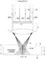
- FIG. 8shows the contrast between a focused Gaussian beam and a Bessel beam incident upon a glass-air-glass composite structure.
- a focused Gaussian beamwill diverge upon entering the first glass layer and will not drill to large depths, or if self-focusing occurs as the glass is drilled, the beam will emerge from the first glass layer and diffract, and will not drill into the second glass layer.
- a Bessel beamwill drill both glass layers over the full extent of the line focus.
- An example of a glass-air-glass composite structure cut with a Bessel beamis shown in the inset photograph in FIG. 8 , which shows a side view of the exposed cut edges.
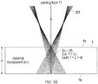
- the top and bottom glass piecesare 0.4 mm thick 2320, CT101.
- the exemplary air gap between two layers of glassis -400 ⁇ m. The cut was made with a single pass of the laser at 200 mm/sec , so that the two pieces of glass were cut simultaneously, even though they were separated by > 400 ⁇ m.
- the air gapis between 50 ⁇ m and 5 mm, for example is between 50 ⁇ m and 2 mm, or between 200 ⁇ m and 2 mm.
- Exemplary disruption layersinclude polyethylene plastic sheeting (e.g., Visqueen ® brand).
- Transparent layersas shown in FIG. 9 , include transparent vinyl (e.g., Penstick brand). Note that unlike with other focused laser methods, to get the effect of a blocking or stop layer, the exact focus does not need to be precisely controlled, nor does the material of the disruption layer need to be particularly durable or expensive. In many applications, one just needs a layer that interferes with the laser light slightly to disrupt the laser light and prevent line focus from occurring.
- Visqueenprevents cutting with the picosecond laser and line focus is a perfect example - other focused picosecond laser beams will most certainly drill right through the Visqueen, and one wishing to avoid drilling right through such a material with other laser methods one would have to very precisely set the laser focus to not be near the Visqueen.
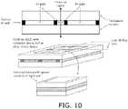
- FIG. 10shows stacking with transparent protective layers to cut multiple sheets while reducing abrasion or contamination. Simultaneously cutting a stack of display glass sheets is very advantageous.
- a transparent polymersuch as vinyl can be placed between the glass sheets.
- the transparent polymer layersserve as protective layers serve to reduce damage to the glass surfaces which are in close contact with one another. These layers would allow the cutting process to work, but would protect the glass sheets from scratching one another, and would furthermore prevent any cutting debris (albeit it is small with this process) from contaminating the glass surfaces.
- the protective layerscan also be comprised of evaporated dielectric layers deposited on the substrates or glass sheets,
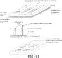
- FIG. 11shows air gap and cutting of encapsulated devices.
- This line focus processcan simultaneously cut through stacked glass sheets, even if a significant macroscopic air gap is present. This is not possible with other laser methods, as illustrated in FIG. 8 .
- Many devicesrequire glass encapsulation, such as OLEDs (organic light emitting diode). Being able to cut through the two glass layers simultaneously is very advantageous for a reliable and efficient device segmentation process. Segmented means one component can be separated from a larger sheet of material that may contain a plurality of other components.
- Other components that can be segmented, cut out, or produced by the methods described hereinare, for example, OLED (organic light emitting diode) components, DLP (digital light processor) components, an LCD (liquid crystal display) cells, semiconductor device substrates.
- FIG. 12shows cutting an article such as electrochromic glass coated with transparent conductive layers (e.g. ITO).
- ITOtransparent conducting layers
- This laser processcan cut through such layers with minimal damage to the transparent conductive layer and very little debris generation.
- the extremely small size of the perforated holes ( ⁇ 5um)means that very little of the ITO will be affected by the cutting process, whereas other cutting methods are going to generate far more surface damage and debris.
- FIG. 13shows precision cutting of some layers in a stack while not damaging others, as also shown in FIG. 1 , extending the concept to multiple layers (i.e., more than two layers).
- the disruption elementis a defocusing layer.
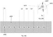
- Fig. 14ashows a schematic top view representation of perforations 1401 formed in a glass substrate 1400 within a heat damaged zone (or heat affected zone) 1403 ( see Fig. 14b ).
- the perforationspreferably extend through the thickness of the glass (but do not have to), can have a particular diameter based on the laser pulse energy, for example, and can be formed by the laser assembly attached to an optical assembly (or by other laser assemblies as may be known or developed that can form such perforations).
- the laser assembly and optical assemblycan have certain predetermined characteristics and functionalities of any and all of the embodiments described herein above, can be preprogrammed and controlled by a controller 1508 as described below, and can preferably provide a single 10 picosecond laser pulse emission (ultra-short pulse laser ablation) to form a defect/perforation along a focal line.
- the perforations 1401can be created on draw, when the glass substrate is hot or can be done after draw at ambient temperature.
- the perforations 1401are shown surrounded by a stress field 1405 including micro cracks 1407 with various lengths (which can be the same length or different lengths).
- the distance D1includes the perforation 1401, the stress field 1405 and all micro cracks 1407 (preferably extends to the end of the longest micro crack).
- Fig. 14bshows a magnified view of D1 showing the local damage site with the perforation 1401, the stress field 1405 and all micro cracks 1407.
- D2is shown as the distance between two perforations 1401, preferably as measured by the center of the perforations 1401.
- a perforationmay not be perfectly lined up and may not have the same diameter (but can have the same diameter and can be lined up) with an adjacent perforation; however, D2 can still be measured.
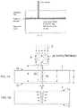
- Fig. 15ashows a laser assembly connected to an optical assembly (roughly shown as a combination at 1505), a moving apparatus 1507 connected to the laser assembly and optical assembly, and a controller 1508 above a side view showing the interface of a glass substrate 1400.
- This figureillustrates the point that these two assemblies (laser and optical) can be attached to the moving apparatus 1507 that is configured to move the laser assembly and optical assembly 1505 with respect to the glass substrate 1400 along the x-axis 1501, the z-axis 1503, and the y-axis (which in Fig. 15a is into and out of the page).
- the controller 1508can be preprogrammed to control 1511 all movements and functionalities described herein and above with respect to (and communicate with) the laser assembly and/or optical assembly 1505.
- the controller 1508can also be preprogrammed to control 1509 all movements and functionalities (and communicate with) of the moving apparatus 1507.
- the control and communication programming and corresponding functionalities of the controller 1508allows the controller 1508 to control these system components to execute instructions representing a predetermined design to create the predetermined design (which can include, but is not limited to, the size of D1 and D2, among other designs described herein).
- Fig 15bshows a magnified side view D1 with the perforation 1401, the stress field 1405, and all micro cracks 1407.
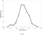
- Fig. 15ccorresponds to Fig. 15b and shows birefringence (retardation (nm), y-axis) due to the stress as function of distance from center of the perforation (x-axis).
- This stressextends, in this exemplary embodiment, +/- 5 ⁇ m from the center of perforation. The highest value indicates highest stress due to the laser induced damage.
- This birefringence graphcan be converted to stress values as shown in Fig. 15d , which shows stress (MPa) vs. location relative to the center of the perforation.
- Stress (MPa)vs. location relative to the center of the perforation.
- Three stress fieldcan be shown" axial stress, radial stress, and hoop stress.
- the tensile stressis the highest in the center of the perforation and, for example, exceeds 100 MPa. Any crack reaching this location will propagate to the center of the perforation.
- the size of stress field and cracks sizecan be adjusted depending on processing conditions.
- the data in Fig. 15dis provided starting at about +/- 1 ⁇ m from the center of perforation.
- the transmission/transfer of data, control signals, and communication signals between the controller 1508, and the laser assembly and/or optical assembly 1505, and the moving apparatus 1507can be implemented over a network, which can be any suitable wired or wireless network capable of transmitting communication, including but not limited to a telephone network, Internet, Intranet, local area network, Ethernet, online communication, offline communications, wireless communications and/or similar communications means.
- the wireless transmissioncan be accomplished through any wireless protocol/technology, including, but not limited to, ZigBee standards-based protocol, Bluetooth technology, and/or Wi-Fi technology.
- the controller 1508can be located in the same room, in a different room in the same building, in a completely different building and location from the laser assembly and/or optical assembly 1505 and the moving apparatus 1507.
- the controller 1508can be programmed to control the laser assembly and/or optical assembly 1505 and/or the moving apparatus 1507 to form perforations 1401 of a particular size, thus forming a particular sized D1 (which can be the same or different in size as compared to a subsequent D1). It is preferable that information such as glass substrate composition/type, size (length, width, and depth) be part of the programming. From the measurement of D1, a "crack length" can be determined, which is defined as D1/2.
- controller 1508can be programmed to control the laser assembly and/or optical assembly 1505 and the moving apparatus 1507 to form subsequent perforations separated by a particular distance D2, D2', and D2", where each of D2, D2', and D2" can be the same distance or different distances as compared to each other.
- the relative interface fracture toughnesscan be tuned by changing the values of D1 (and hence, crack length which equals D1/2) and D2.
- the controller 1508can be programmed to create optimally sized crack lengths (D1/2) and optimally spaced-apart perforations (D2, D2' etc.) along an interface defining a contour (in accordance with the advantages discussed, supra).
- Fig. 16a graphical illustration showing relative interface fracture toughness vs. average of the distances between perforation sites (D2)/average of the averaged characteristic crack lengths of each perforation site (D1/2) is provided.
- G1glass-1 high strength (e.g., Eagle XG ® glass)
- G2glass-2 intermediate strength (e.g., untempered soda-lime glass)
- G3glass-3 low strength (e.g., the tension layer of ion-exchanged (Gorilla ® ) or thermally tempered soda-lime glass). It is preferable to obtain an average crack length for each formed perforation, and then to determine an average of the averaged crack lengths for the equation shown in Fig.
- An average crack length of a single perforationcan be determined, for example, by taking the average of three measurements along the perforation in three different places.
- tempered glassboth ion-exchanged as well as thermally tempered
- a crack in the tension layerpropagates easier than glass without this tension layer (untempered glass).
- the relative fracture toughness valuesare normalized across all glass types. For example, a relative interface fracture toughness measurement of 1 has approximately the same strength as a pristine version of the particular glass that is to be processed with perforations.
- a relative interface fracture toughness under 0.2typically means that the glass will spontaneously separate along an interface defining a contour defined by a series of spaced-apart perforations 1401. This can happen, for example, when the perforation sites are very close together (e.g., overlapping).
- a relative interface fracture toughness between 0.2 and 0.8is a range that can be deemed an optimum range. For example, if an easier separation along the contour is desired, then a relative interface fracture toughness closer to 0.2, for example, can be obtained. On the other hand, if a stronger relative interface fracture toughness is desired close to but not including a pristine glass value of 1, then a relative interface fracture toughness closer to 0.8, for example can be obtained and so on.
- the specifics about the (1) particular glass (glass substrate composition/type, size (length, width, and depth), (2) desired relative interface fracture toughness, and (3) in turn, the average distances between perforation sites (D2) and the average of the averaged characteristic crack lengths (D1/2)be determined.
- Actual average distances and crack length valuesare shown in Figs. 17a-b to further illustrate these points, and are further discussed below.
- Figs. 17a-bare similar to Fig. 16 , in the sense that the controller 1508 can be programmed to create a desired relative interface fracture toughness in view of the particulars of the subject glass substrate and the average of the distances between perforation sites, where, for example, in Fig. 17a - the average of the averaged crack lengths of each perforation site is a particular value such as 1 micron, 1.5 microns, and 2 microns, and in Fig. 17b - the average of the averaged crack lengths of each perforation site is a particular value such as 5 microns, 10 microns, 20 microns, 30 microns, and 40 microns.
- Figs. 16 and 17a-bare not the only respective values contemplated by this embodiment that can be used, nor the only particular glass compositions. This embodiment contemplates other values and other compositions, and still be within and supported by the teaching of this embodiment.
- Figs. 16 and 17a-bonly show examples. For each glass processing situation, one may expect to generate curve similar to that shown in Figs. 16 or 17a-b .
- Preferable desired spacing between the perforation sites D2can be at a range to result in 30-80% reduction of the interface toughness for proposed subsequent induced separation.
- Figs. 16 and 17a-bThe values along the x-axis and resulting values along the y-axis forming the curves shown in Figs. 16 and 17a-b were determined by experimentation (computer model and/or actual experimental testing). For example, a four point bend procedure for strength testing of glass substrates is performed (this procedure in general should be understood and appreciated by those of skill in the art) to determine the force required to separate a glass substrate along an interface contour created by a plurality of formed spaced-apart perforations (with particular crack lengths and which are separated from one another by particular distances).
- samples50 mm length x 50 mm width x 0.7 mm thickness are tested for strength (load to failure) using the four point bending test.
- These samplescan include a pristine glass sample with no perforations formed therein (as a control), glass samples with perforations formed along a contour (per the system and methods described herein) with each glass sample having a different spacing between subsequent perforations and different crack lengths.
- An Instron model 5343 single column testing instrument with Bluehill 2 softwareis used. Samples are covered with tape (471 vinyl tape) on the compression side. Samples are placed flat, centered and square on the support span having distance of 3.6 cm, a load is applied at a rate of 5 mm/min with the load span having a distance of 1.8 mm.
- Test temperatureis about 22°C and 50% relative humidity. Typically a minimum of 20 samples are tested for load to failure. The data is then plotted as load (lbs or N force) and/or strength to failure (psi or MPa). The results of such experimentations are normalized to a pristine (non-perforated) glass (of each glass type, i.e., G1, G2, and G3, as described above) and then plotted in Figs. 16-17a-b .
- a top view of glass 1400is shown illustrating the start of separation of the glass 1400 at 1801 into components 1803 and 1805 on opposite sides of the contour 1807.
- the separation at 1801can generally start at the top of the glass 1400 (e.g., with a mechanical tool or by thermal or mechanical scoring then separating, as should be appreciated by those skilled in the art) and work its way to the bottom of glass 1400.
- the absolute relative interface fracture toughness value of the glass substrate 1400 produced by the crack length and D2 positioningwill determine how easy it is to separate the glass into components 1803 and 1805 (which should preferably be valued somewhere between 0.2 and 0.8).
- Fig. 19shows a SEM image of a side view of the interface of a glass substrate 1400 post perforation 1401 formation and separation. D1 is shown at about 2 microns and D2 is shown at about 8 microns.
- a specific example where glass is perforated with optimized spacing such as > 100 um in distancecan be done at an appropriate translation speed of the laser beam with given repetition rate of the laser.
- the laser repletion rateis 200 kHz, but can be modulated at some lower rate to about 10 Khz.
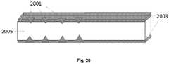
- An optionis to create damage only in a CS layer 2003 or both CS layers 2003, without affecting the CT layer 2005 of a glass substrate ( see Fig. 20 ). This may broaden the window of the spacing available for the perforation.
- the HAZ zonewill be significantly smaller, and hoop stress may be smaller as well.
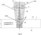
- Fig. 21an alternative optical assembly 6 is shown.
- the embodiment shown in Fig. 21is similar to Fig. 4 (the similarities will not be described again here), except that a portion of the optical assembly 6 includes a reflective coating 2105.
- the reflective coating 2105is placed on the surface of the optical assembly 6.
- the reflective coating 2105is configured to block some of the laser radiation 2a (as shown by dashed lines 2107) directed to layer 1 along focal line 2b resulting in a defects closer to the surfaces 1a and 1b of the layer 1 along the focal line 2b at areas of extensive induced absorption 2c, and not in the center of the layer 1 (as shown by dashed lines 2019).
- the center of layer 1 along the focal line 2breceives less intensity of laser radiation 2a from a laser pulse resulting in substantially less to preferably no induced absorption 2c (and, thus, substantially less to preferably no cracking in/damage to layer 1 at 2109).
- aspects of particular embodimentsmay be embodied/implemented as a computer system, method or computer program product.
- the computer program productcan have a computer processor or neural network, for example, which carries out the instructions of a computer program.
- aspects of particular embodimentsmay take the form of an entirely hardware embodiment, an entirely software embodiment, and entirely firmware embodiment, or an embodiment combining software/firmware and hardware aspects that may all generally be referred to herein as a "circuit,” “module,” “system,” or an “engine.”
- aspects of particular embodimentsmay take the form of a computer program product embodied in one or more computer readable medium(s) having computer readable program code embodied thereon.
- the computer readable mediummay be a computer readable signal medium or a computer readable storage medium.
- a computer readable storage mediummay be, for example, but not limited to, an electronic, magnetic, optical, electromagnetic, infrared, or semiconductor system, apparatus, or device, or any suitable combination of the foregoing.
- a computer readable storage mediummay be any tangible medium that can contain, or store a program for use by or in connection with an instruction performance system, apparatus, or device.
Landscapes
- Engineering & Computer Science (AREA)
- Physics & Mathematics (AREA)
- Optics & Photonics (AREA)
- Chemical & Material Sciences (AREA)
- Plasma & Fusion (AREA)
- Mechanical Engineering (AREA)
- General Chemical & Material Sciences (AREA)
- Chemical Kinetics & Catalysis (AREA)
- Oil, Petroleum & Natural Gas (AREA)
- Organic Chemistry (AREA)
- Materials Engineering (AREA)
- Laser Beam Processing (AREA)
- Re-Forming, After-Treatment, Cutting And Transporting Of Glass Products (AREA)
Description
- The embodiments disclosed herein relate to methods, systems, and system components for creating and arranging small (micron and smaller) defects or perforations in transparent materials in a particular manner, and, more particularly, to the arrangement of these defects, each of which has an average crack length, in a predetermined spaced-apart relation (each defect separated from an adjacent defect by a predetermined distance) defining a contour in a transparent material to lower the relative interface fracture toughness for subsequent planned induced separation.
- In recent years, precision micromachining and related process improvements to meet customer demands to reduce the size, weight and material cost of leading-edge devices has led to fast pace growth in high-tech industries in flat panel displays for touch screens, tablets, smartphones and televisions. Moreover, ultrafast industrial lasers are becoming important tools for applications requiring high precision micromachining.
- Relatively large glass sheets/substrates are typically delivered to manufacturers; and thus, they need to be cut into smaller sizes before being further processed. (Such processing may include additional layers of coating, thin film transistors ("TFTs") or other value adding attributes of the glass surface. In many conventional laser glass cutting processes, the separation of glass into smaller sheets relies on laser scribing or perforation followed by separation with mechanical force or thermal stress-induced crack propagation. Nearly all current laser cutting techniques exhibit one or more shortcomings, including: (1) limitations in their ability to perform a free form shaped cut of thin glass on a carrier due to a large heat-affected zone associated with the long laser pulses (nanosecond scale or longer) used for cutting; (2) production of thermal stress that often results in cracking of the glass surface near the region of laser illumination due to the generation of shock waves and uncontrolled material removal; (3) difficulties in controlling the depth of the cut (e.g., to within tens of microns); and/or (4) creation of sub-surface damage in the glass that extends hundreds of microns (or more) glass below the surface of the glass, resulting in defect sites at which crack propagation can initiate.
- Some glasses are easily separated with conventional tools such as mechanical cutting equipment, or CO2 laser cutting processes. Some glasses are difficult to cut using these techniques, and more complicated and sophisticated equipment may be needed. For example, mechanically or chemically strengthened glasses are difficult to cut using the aforementioned mechanical tools or CO2 lasers. Thin glasses (< 0.2 mm thick) are another example of glasses that are difficult to cut using conventional equipment. Glass-ceramics and other transparent materials characterized by a high fracture toughness are also difficult to separate using conventional mechanical tools. Accordingly, there is a need to address the aforementioned issues and provide improved glass separation equipment and techniques.
US 2013/126573 A1 discloses a method for the internal processing of a transparent substrate in preparation for a cleaving step.US 2013/068736 A1 discloses systems and methods for material singulation.EP 0938946 A1 discloses a method for cleaving a strip by a thermal stress.US 2007/202619 A1 discloses a laser processing apparatus having one laser light source that simultaneously radiates laser beams with two wavelengths. - The embodiments disclosed herein relate to a method and an apparatus to create small (micron and smaller) "holes" in transparent materials (glass, sapphire, etc) for the purpose of drilling, cutting, separating, perforating, or otherwise processing the materials. More particularly, an ultrashort (i.e., from 10-10 to 10-15 second) pulse laser beam (wavelengths such as 1064, 532, 355 or 266 nanometers) is focused to an energy density above the threshold needed to create a defect in the region of focus at the surface of or within the transparent material. By repeating the process, a series of laser-induced defects aligned along a predetermined path can be created. By spacing the laser-induced features sufficiently close together, a controlled region of mechanical weakness within the transparent material can be created and the transparent material can be precisely fractured or separated (mechanically or thermally) along the path defined by the series of laser-induced defects. The ultrashort laser pulse(s) may be optionally followed by a carbon dioxide (CO2) laser or other source of thermal stress to effect fully automated separation of a transparent material or part from a substrate substrate, for example.
- In certain applications where transparent materials are bonded together to form a stack or layered structure, it is often desirable to selectively "cut" to the boundary of a particular layer without disturbing underlying layers. This may be performed with the addition of a reflective or absorptive (for the desired wavelength) material or layer at the preferred depth of cut. A reflective layer may be formed by depositing a thin material (aluminum, copper, silver, gold, etc). A reflective layer is preferential as it scatters the incident energy (as opposed to absorbing and thermally dissipating the incident energy). In this manner, the depth of the cut may be controlled with no damage to the underlying layers. In one application, a transparent material is bonded to a carrier substrate and a reflective or absorptive layer is formed between the transparent material and carrier substrate. The reflective or absorptive layer enables cutting of the transparent material without damage to the underlying carrier substrate, which may then be reused.
- In a first aspect of the invention, a system is provided as defined in
claim 1. - In a second aspect, a method as defined in claim 9.
- Advantages of perforating glass substrates according to the various embodiments described herein include, but art not limited to, (i) providing a glass substrate with a lowered relative fracture toughness (created by the optimally sized and spaced-apart perforations along an interface defining a contour), and (ii) being able to handle and transport the perforated glass substrate as a monolithic piece until subsequent separation to predetermined dimensions by any known or to be developed separation equipment or technique along the contour is desired/required (and before or after processing of any kind, such as films deposition). Stated differently, forming the optimally sized and spaced-apart perforations allow for tuning of the relative interface fracture toughness of a glass substrate (no matter the type of glass), so that the relative toughness is high enough that the glass does not spontaneously separate (propagation of a crack) along the contour during transport, for example, yet is low enough making separation along the interface/contour easier than without the perforations being present. This way, a mechanical scribe or thermally induced stress, for example, can lead to crack propagation along these created earlier damage sites when needed/desired. As a result the glass piece can be perforated (as needed upon demand) with such sites along desired future separation lines. This perforated glass can be processed as a solid piece, and separated after processing.
- Additional features and advantages will be set forth in the detailed description which follows, and in part will be readily apparent to those skilled in the art from that description or recognized by practicing the embodiments as described herein, including the detailed description which follows, the claims, as well as the appended drawings.
- It is to be understood that both the foregoing general description and the following detailed description are merely exemplary, and are intended to provide an overview or framework to understanding the nature and character of the claims. The accompanying drawings are included to provide a further understanding, and are incorporated in and constitute a part of this specification. The drawings illustrate one or more embodiment(s), and together with the description serve to explain principles and operation of the various embodiments
- The foregoing will be apparent from the following more particular description of the example embodiments, as illustrated in the accompanying drawings in which like reference characters refer to the same parts throughout the different views. The drawings are not necessarily to scale, emphasis instead being placed upon illustrating the representative embodiments.
Figure 1 is an illustration of a stack of three layers according to an embodiment: a thin material A facing the laser energy, a modified interface, and a thick material B, the modified interface disrupting the laser energy form interacting with the portion of the stack on the side of the modified interface remote from the laser beam;Figures 2A and 2B are illustrations showing the positioning of a laser beam focal line according to an embodiment;Figure 3A is an illustration of an optical assembly for laser processing according to an embodiment;Figures 3B-1, 3B-2, 3B-3, and 3B-4 illustrate various possibilities for processing the substrate by forming the laser beam focal line at different positions within the transparent material relative to the substrate according to embodiments;Figure 4 is an illustration of a second optical assembly for laser processing according to an embodiment;Figures 5A and5B are illustrations of a third optical assembly for laser drilling according to an embodiment;Figure 6 is a schematic illustration of a fourth optical assembly for laser processing according to an embodiment;Figure 7 is a graph of laser emission as a function of time for a picosecond laser according to an embodiment, where each emission is characterized by a pulse "burst" which may contain one or more sub-pulses, the frequency of the bursts is the repetition rate of the laser, typically about 100 kHz (10 µsec), and the time between sub-pulses is much shorter, e.g., about 20 nanoseconds (nsec);Figure 8 is a comparison between a focused Gaussian beam and a Bessel beam incident upon a glass-air-glass composite structure;Figure 9 is an illustration of stacking with transparent protective layers to cut multiple sheets while reducing abrasion or contamination according to an embodiment;Figure 10 is an illustration of an air gap and cutting of encapsulated devices according to an embodiment;Figure 11 is an illustration of cutting of interposers or windows with laser perforation then etch or laser perforation and CO2 laser release according to an embodiment;Figure 12 is an illustration of cutting an article such as electrochromic glass coated with transparent conductive layers (e.g. indium tin oxide (ITO)) according to an embodiment;Figure 13 is an illustration of precision cutting of some layers in a stack while not damaging others according to an embodiment;Figure 14a is a schematic top view representation of perforations formed in a glass substrate according to an embodiment;Figure 14b is a magnified view of D1 shown inFig. 14a showing the local damage site with the perforation, the stress field and all micro cracks in a glass substrate according to an embodiment;Figure 15a is a side view of a glass substrate showing the interface of the glass substrate, a laser assembly connected to an optical assembly, a moving apparatus connected to the laser assembly and/or optical assembly, and a controller above the glass substrate according to an embodiment;Figure 15b is a magnified side view of D1 shown inFig. 15a showing the local damage site with the perforation, the stress field and all micro cracks in a glass substrate according to an embodiment;Figure 15c is an illustrates of birefringence (retardation (nm),) due to the stress as function of distance from center of the perforation (x-axis).Figure 15d corresponds toFigure 15c and illustrates stress values as function of distance from center of the perforation (x-axis).Figure 16 is a graphical illustration showing relative interface fracture toughness vs. average of the distances between perforation sites (D2)/average of the averaged characteristic crack lengths (D1/2) according to an embodiment;Figures 17a-b are graphical illustrations showing relative interface fracture toughness of G2 = glass-2 intermediate strength glass vs. actual average of the distances between perforation sites (D2) where actual particular averaged crack lengths are involved according to an embodiment;Figure 18 is a top view of a glass substrate illustrating the start of separation of the glass into components on opposite sides of a contour according to an embodiment;Figure 19 is a SEM image of a side view of the interface of a glass substrate post perforation formation and separation according to an embodiment;Figure 20 is a side view of a glass substrate showing the creation of damage only in at least one CS layer, without affecting the CT layer of a glass substrate according to an embodiment; andFig. 21 is an illustration of an alternative optical assembly for laser processing according to an embodiment.- A description of example embodiments follows.
- The embodiment described herein relates to a method and apparatus for optically producing high precision cuts in or through transparent materials. Sub-surface damage may be limited to the order of 60 microns in depth or less, and the cuts may produce only low debris. Cutting of a transparent material with a laser in accordance with the present disclosure may also be referred to herein as drilling or laser drilling or laser processing. A material is substantially transparent to the laser wavelength when the absorption is less than about 10%, preferably less than about 1% per mm of material depth at this wavelength.
- In accordance with methods described below, in a single pass, a laser can be used to create highly controlled full line perforation through the material, with extremely little (<75µm, often <50µm) subsurface damage and debris generation. This is in contrast to the typical use of spot-focused laser to ablate material, where multiple passes are often necessary to completely perforate the glass thickness, large amounts of debris are formed from the ablation process, and more extensive sub-surface damage (>100µm) and edge chipping occur.
- Thus, it is possible to create a microscopic (i.e., < 0.5 µm and > 100 nm in diameter) elongated "hole" (also called a perforation or a defect line) in transparent material using a single high energy burst pulse. These individual perforations can be created at rates of several hundred kilohertz (several hundred thousand perforations per second, for example). Thus, with relative motion between the source and the material these perforations can be placed adjacent to one another (spatial separation varying from sub-micron to several microns as desired). This spatial separation is selected in order to facilitate cutting. In some embodiments the defect line is a "through hole", which is a hole or an open channel that extends from the top to the bottom of the transparent material. In some embodiments the defect line may not be a continuous channel, and may be blocked or partially blocked by portions or sections of solid material (e.g., glass). As defined herein, the internal diameter of the defect line is the internal diameter of the open channel or the air hole. For example, in the embodiments described herein the internal diameter of the defect line is < 500nm, for example ≤ 400 nm, or ≤ 300 nm. The disrupted or modified area (e.g., compacted, melted, or otherwise changed) of the material surrounding the holes in the embodiments disclosed herein, preferably has diameter of < 50 µm (e.g., < 10 µm).
- In addition, through judicious selection of optics, selective cut individual layers of stacked transparent materials. Micromachining and selective cutting of a stack of transparent materials is accomplished with precise control of the depth of cut through selection of an appropriate laser source and wavelength along with beam delivery optics, and the placement of a beam disruption element at the boundary of a desired layer. The beam disruption element may be a layer of material or an interface. The beam disruption element may be referred to herein as a laser beam disruption element, disruption element or the like. Embodiments of the beam disruption element may be referred to herein as a beam disruption layer, laser beam disruption layer, disruption layer, beam disruption interface, laser beam disruption interface, disruption interface, or the like.
- The beam disruption element reflects, absorbs, scatters, defocuses or otherwise interferes with an incident laser beam to inhibit or prevent the laser beam from damaging or otherwise modifying underlying layers in the stack. In one embodiment, the beam disruption element underlies the layer of transparent material in which laser drilling will occur. As used herein, the beam disruption element underlies the transparent material when placement of the beam disruption element is such that the laser beam must pass through the transparent material before encountering the beam disruption element. The beam disruption element may underlie and be directly adjacent to the transparent layer in which laser drilling will occur. Stacked materials can be micro-machined or cut with high selectivity by inserting a layer or modifying the interface such that a contrast of optical properties exists between different layers of the stack. By making the interface between materials in the stack more reflective, absorbing, and/or scattering at the laser wavelengths of interest, cutting can be confined to one portion or layer of the stack.
- The wavelength of the laser is selected so that the material within the stack to be laser processed (drilled, cut, ablated, damaged or otherwise appreciably modified by the laser) is transparent to the laser wavelength. In one embodiment, the material to be processed by the laser is transparent to the laser wavelength if it absorbs less than 10% of the intensity of the laser wavelength per mm of thickness of the material. In another embodiment, the material to be processed by the laser is transparent to the laser wavelength if it absorbs less than 5% of the intensity of the laser wavelength per mm of thickness of the material. In still another, the material to be processed by the laser is transparent to the laser wavelength if it absorbs less than 2% of the intensity of the laser wavelength per mm of thickness of the material. In yet another embodiment, the material to be processed by the laser is transparent to the laser wavelength if it absorbs less than 1% of the intensity of the laser wavelength per mm of thickness of the material.
- The selection of the laser source is further predicated on the ability to induce multi-photon absorption (MPA) in the transparent material. MPA is the simultaneous absorption of multiple photons of identical or different frequencies in order to excite a material from a lower energy state (usually the ground state) to a higher energy state (excited state). The excited state may be an excited electronic state or an ionized state. The energy difference between the higher and lower energy states of the material is equal to the sum of the energies of the two photons. MPA is a third-order nonlinear process that is several orders of magnitude weaker than linear absorption. It differs from linear absorption in that the strength of absorption depends on the square of the light intensity, thus making it a nonlinear optical process. At ordinary light intensities, MPA is negligible. If the light intensity (energy density) is extremely high, such as in the region of focus of a laser source (particularly a pulsed laser source), MPA becomes appreciable and leads to measurable effects in the material within the region where the energy density of the light source is sufficiently high. Within the focal region, the energy density may be sufficiently high to result in ionization.
- At the atomic level, the ionization of individual atoms has discrete energy requirements. Several elements commonly used in glass (e.g., Si, Na, K) have relatively low ionization energies (~5 eV). Without the phenomenon of MPA, a wavelength of about 248 nm would be required to create linear ionization at ~5 eV. With MPA, ionization or excitation between states separated in energy by ~5 eV can be accomplished with wavelengths longer than 248 nm. For example, photons with a wavelength of 532 nm have an energy of ~2.33 eV, so two photons with wavelength 532 nm can induce a transition between states separated in energy by ~4.66 eV in two-photon absorption (TPA), for example.
- Thus, atoms and bonds can be selectively excited or ionized in the regions of a material where the energy density of the laser beam is sufficiently high to induce nonlinear TPA of a laser wavelength having half the required excitation energy, for example. MPA can result in a local reconfiguration and separation of the excited atoms or bonds from adjacent atoms or bonds. The resulting modification in the bonding or configuration can result in non-thermal ablation and removal of matter from the region of the material in which MPA occurs. This removal of matter creates a structural defect (e.g. a defect line or "perforation") that mechanically weakens the material and renders it more susceptible to cracking or fracturing upon application of mechanical or thermal stress. By controlling the placement of perforations, a contour or path along which cracking occurs can be precisely defined and precise micromachining of the material can be accomplished. The contour defined by a series of perforations may be regarded as a fault line and corresponds to a region of structural weakness in the material. In one embodiment, micromachining includes separation of a part from the material processed by the laser, where the part has a precisely defined shape or perimeter determined by a closed contour of perforations formed through MPA effects induced by the laser. As used herein, the term closed contour refers to a perforation path formed by the laser line, where the path intersects with itself at some location. An internal contour is a path formed where the resulting shape is entirely surrounded by an outer portion of material.
- Perforations can be accomplished with a single "burst" of high energy short duration pulses spaced close together in time. The laser pulse duration may be 10-10 s or less, or 10-11 s or less, or 10-12 s or less, or 10-13 s or less. These "bursts" may be repeated at high repetition rates (e.g. kHz or MHz). The perforations may be spaced apart and precisely positioned by controlling the velocity of a substrate or stack relative to the laser through control of the motion of the laser and/or the substrate or stack.
- As an example, in a thin transparent substrate moving at 200 mm/sec exposed to a 100 kHz series of pulses, the individual pulses would be spaced 2 microns apart to create a series of perforations separated by 2 microns. This defect (perforation) spacing is sufficient close to allow for mechanical or thermal separation along the contour defined by the series of perforations.
- In some cases, a fault line created along a contour defined by a series of perforations or defect lines is not enough to separate the part spontaneously, and a secondary step may be necessary. If so desired, a second laser can be used to create thermal stress to separate it, for example. In the case of sapphire, separation can be achieved, after the creation of a fault line, by application of mechanical force or by using a thermal source (e.g., an infrared laser, for example a CO2 laser) to create thermal stress and force a part to separate from a substrate. Another option is to have the CO2 laser only start the separation and then finish the separation manually. The optional CO2 laser separation can be achieved, for example, with a defocused continuous wave (cw) laser emitting at 10.6 µm and with power adjusted by controlling its duty cycle. Focus change (i.e., extent of defocusing up to and including focused spot size) is used to vary the induced thermal stress by varying the spot size. Defocused laser beams include those laser beams that produce a spot size larger than a minimum, diffraction-limited spot size on the order of the size of the laser wavelength. For example, spot sizes of about 7 mm, 2 mm and 20 mm can be used for CO2 lasers, for example, whose emission wavelength is much smaller at 10.6 µm. Distance between adjacent defect lines 120 along the direction of the fault lines 110 can be greater than 0.5 µm and less than or equal to about 15 µm in some embodiments, for example.
- Acid etching can be used, for example, to separate a workpiece having a glass layer, for example. To enlarge the holes to a size useful for metal filling and electrical connections, parts can be acid etched. In one embodiment, for example, the acid used can be 10% HF /15% HNO3 by volume. The parts can be etched for 53 minutes at a temperature of 24-25 °C to remove about 100 µm of material, for example. The parts can be immersed in this acid bath, and ultrasonic agitation at a combination of 40 kHz and 80 kHz frequencies can used to facilitate penetration of fluid and fluid exchange in the holes. In addition, manual agitation of the part within the ultrasonic field can be made to prevent standing wave patterns from the ultrasonic field from creating "hot spots" or cavitation related damage on the part. The acid composition and etch rate can be intentionally designed to slowly etch the part - a material removal rate of only 1.9um/minute, for example. An etch rate of less than about 2 µm/minute, for example, allows acid to fully penetrate the narrow holes and agitation to exchange fresh fluid and remove dissolved material from the holes which are initially very narrow.
- In the embodiment shown in
FIG. 1 , precise control of the depth of cut in a multilayer stack is achieved by inclusion of a beam disruption interface (labeled "modified interface"). The beam disruption interface prevents the laser radiation from interacting with portions of the multilayer stack beyond the position of the disruption interface. - In one embodiment, the beam disruption element is positioned immediately below the layer of the stack in which modification via two-photon absorption will occur. Such a configuration is shown in
Fig. 1 , where the beam disruption element is a modified interface positioned immediately below material A and material A is the material in which formation of perforations through the two-photon absorption mechanism described herein will occur. As used herein, reference to a position below or lower than another position assumes that the top or uppermost position is the surface of the multilayer stack upon which the laser beam is first incident. InFig. 1 , for example, the surface of material A that is closest to the laser source is the top surface and placement of the beam disruption element below material A means that the laser beam traverses material A before interacting with the beam disruption element. - The disruption element has different optical properties than the material to be cut. For example, the beam disruption element may be a defocusing element, a scattering element, a translucent element, or a reflective element. A defocusing element is an interface or a layer comprising a material that prevents the laser light from forming the laser beam focal line on or below the defocusing element. The defocusing element may be comprised of a material or interface with refractive index inhomogeneities that scatter or perturb the wavefront of the optical beam. A translucent element is an interface or layer of material that allows light to pass through, but only after scattering or attenuating the laser beam to lower the energy density sufficiently to prevent formation of a laser beam focal line in portions of the stack on the side of the translucent element that are remote from the laser beam. In one embodiment, the translucent element effects scattering or deviating of at least 10% of the light rays of the laser beam.
- More specifically, the reflectivity, absorptivity, defocusing, attenuation, and/or scattering of the disruption element can be employed to create a barrier or impediment to the laser radiation. The laser beam disruption element can be created by several means. If the optical properties of the overall stack system are not of a concern, then one or more thin films can be deposited as a beam disruption layer(s) between the desired two layers of the stack, where the one or more thin films absorb, scatter, defocus, attenuate, reflects, and/or dissipates more of the laser radiation than the layer immediately above it to protect layers below the thin film(s) from receiving excessive energy density from the laser source. If the optical properties of the entire stack system do matter, the beam disruption element can be implemented as a notch filter. This can be done by several methods:
- creating structures at the disruption layer or interface (e.g. via thin film growth, thin film patterning, or surface pattering) such that diffraction of incident laser radiation is at a particular wavelength or range of wavelengths occurs;
- creating structures at the disruption layer or interface (e.g. via thin film growth, thin film patterning, or surface pattering) such that scattering of incident laser radiation occurs (e.g. a textured surface);
- creating structures at the disruption layer or interface (e.g. via thin film growth, thin film patterning, or surface pattering) such that attenuated phase-shifting of laser radiation occurs; and
- creating a distributed Bragg reflector via thin-film stack at the disruption layer or interface to reflect only laser radiation.
- It is not necessary that the absorption, reflection scattering, attenuation, defocusing etc. of the laser beam by the disruption element be complete. It is only necessary that the effect of the disruption element on the laser beam is sufficient to reduce the energy density or intensity of the focused laser beam to a level below the threshold required for cutting, ablation, perforating etc. of the layers in the stack protected by (underlying) the disruption element. In one embodiment, the disruption element reduces the energy density or intensity of the focused laser beam to a level below the threshold needed to induce two-photon absorption. The disruption layer or disruption interface may be configured to absorb, reflect, or scatter the laser beam, where the absorption, reflection, or scattering are sufficient to reduce the energy density or intensity of the laser beam transmitted to the carrier (or other underlying layer) to a level below the level needed to induce nonlinear absorption in the carrier or underlying layer.
- Turning to
FIGS. 2A and 2B , a method of laser drilling a material includes focusing apulsed laser beam 2 into a laser beamfocal line 2b, viewed along the beam propagation direction. Laser beamfocal line 2b is a region of high energy density. As shown inFIG. 3 , laser 3 (not shown) emitslaser beam 2, which has aportion 2a incident tooptical assembly 6. Theoptical assembly 6 turns the incident laser beam into an extensive laser beamfocal line 2b on the output side over a defined expansion range along the beam direction (length 1 of the focal line). Layer 1 is the layer of a multilayer stack in which internal modifications by laser processing and two-photon absorption is to occur.Layer 1 is a component of a larger workpiece, which typically includes a substrate or carrier upon which a multilayer stack is formed.Layer 1 is the layer within the multilayer stack in which holes, cuts, or other features are to be formed through two-photon absorption assisted ablation or modification as described herein. Thelayer 1 is positioned in the beam path to at least partially overlap the laser beamfocal line 2b oflaser beam 2.Reference 1a designates the surface of thelayer 1 facing (closest or proximate to) theoptical assembly 6 or the laser, respectively,reference 1b designates the reverse surface of layer 1(the surface remote, or further away from,optical assembly 6 or the laser). The thickness of the layer 1 (measured perpendicularly to theplanes - As
FIG. 2A depicts,layer 1 is aligned perpendicular to the longitudinal beam axis and thus behind the samefocal line 2b produced by the optical assembly 6 (the substrate is perpendicular to the plane of the drawing). Viewed along the beam direction, thelayer 1 is positioned relative to thefocal line 2b in such a way that thefocal line 2b (viewed in the direction of the beam) starts before thesurface 1a of thelayer 1 and stops before thesurface 1b of thelayer 1, i.e.focal line 2b terminates within thelayer 1 and does not extend beyondsurface 1b. In the overlapping area of the laser beamfocal line 2b withlayer 1, i.e. in the portion oflayer 1 overlapped byfocal line 2b, the extensive laser beamfocal line 2b generates nonlinear absorption inlayer 1. (Assuming suitable laser intensity along the laser beamfocal line 2b, which intensity is ensured by adequate focusing oflaser beam 2 on a section of length l (i.e. a line focus of length 1), which defines anextensive section 2c (aligned along the longitudinal beam direction) along which an induced nonlinear absorption is generated in thelayer 1.) The induced nonlinear absorption results in formation of a defect line or crack inlayer 1 alongsection 2c. The defect or crack formation is not only local, but rather may extend over the entire length of theextensive section 2c of the induced absorption. The length ofsection 2c (which corresponds to the length of the overlapping of laser beamfocal line 2b with layer 1) is labeled with reference L. The average diameter or extent of the section of the inducedabsorption 2c (or the sections in the material oflayer 1 undergoing the defect line or crack formation) is labeled with reference D. This average extent D basically corresponds to the average diameter δ of the laser beamfocal line 2b, that is, an average spot diameter in a range of between about 0.1 µm and about 5 µm. - As
FIG. 2A shows, the layer 1 (which is transparent to the wavelength λ of laser beam 2) is locally heated due to the induced absorption along thefocal line 2b. The induced absorption arises from the nonlinear effects associated with the high intensity (energy density) of the laser beam withinfocal line 2b.FIG. 2B illustrates that theheated layer 1 will eventually expand so that a corresponding induced tension leads to micro-crack formation, with the tension being the highest atsurface 1a. - Representative
optical assemblies 6, which can be applied to generate thefocal line 2b, as well as a representative optical setup, in which these optical assemblies can be applied, are described below. All assemblies or setups are based on the description above so that identical references are used for identical components or features or those which are equal in their function. Therefore only the differences are described below. - To insure high quality (regarding breaking strength, geometric precision, roughness and avoidance of re-machining requirements) of the surface of separation after cracking along the contour defined by the series of perforations, the individual focal lines used to form the perforations that define the contour of cracking should be generated using the optical assembly described below (hereinafter, the optical assembly is alternatively also referred to as laser optics). The roughness of the separated surface is determined primarily by the spot size or the spot diameter of the focal line. A roughness of a surface can be characterized, for example, by an Ra surface roughness statistic (roughness arithmetic average of absolute values of the heights of the sampled surface). In order to achieve a small spot size of, for example, 0.5 µm to 2 µm in case of a given wavelength λ of laser 3 (interaction with the material of layer 1), certain requirements must usually be imposed on the numerical aperture of
laser optics 6. These requirements are met bylaser optics 6 described below. - In order to achieve the required numerical aperture, the optics must, on the one hand, dispose of the required opening for a given focal length, according to the known Abbé formulae (N.A. = n sin (theta), n: refractive index of the material to be processed, theta: half the aperture angle; and theta = arctan (D/2f); D: aperture, f: focal length). On the other hand, the laser beam must illuminate the optics up to the required aperture, which is typically achieved by means of beam widening using widening telescopes between the laser and focusing optics.
- The spot size should not vary too strongly for the purpose of a uniform interaction along the focal line. This can, for example, be ensured (see the embodiment below) by illuminating the focusing optics only in a small, circular area so that the beam opening and thus the percentage of the numerical aperture only vary slightly.
- According to
FIG. 3A (section perpendicular to the substrate plane at the level of the central beam in the laser beam bundle oflaser radiation 2; here, too,laser beam 2 is perpendicularly incident to thelayer 1, i.e. incidence angle β is 0° so that thefocal line 2b or the extensive section of the inducedabsorption 2c is parallel to the substrate normal), thelaser radiation 2a emitted bylaser 3 is first directed onto acircular aperture 8 which is completely opaque to the laser radiation used.Aperture 8 is oriented perpendicular to the longitudinal beam axis and is centered on the central beam of the depictedbeam bundle 2a. The diameter ofaperture 8 is selected in such a way that the beam bundles near the center ofbeam bundle 2a or the central beam (here labeled with 2aZ) hit the aperture and are completely blocked by it. Only the beams in the outer perimeter range ofbeam bundle 2a (marginal rays, here labeled with 2aR) are not blocked due to the reduced aperture size compared to the beam diameter, but passaperture 8 laterally and hit the marginal areas of the focusing optic elements of theoptical assembly 6, which, in this embodiment, is designed as a spherically cut, bi-convex lens 7. - Lens 7 is centered on the central beam and is designed as a non-corrected, bi-convex focusing lens in the form of a common, spherically cut lens. The spherical aberration of such a lens may be advantageous. As an alternative, aspheres or multi-lens systems deviating from ideally corrected systems, which do not form an ideal focal point but a distinct, elongated focal line of a defined length, can also be used (i.e., lenses or systems which do not have a single focal point). The zones of the lens thus focus along a
focal line 2b, subject to the distance from the lens center. The diameter ofaperture 8 across the beam direction is approximately 90% of the diameter of the beam bundle (defined by the distance required for the intensity of the beam to decrease to 1/e of the peak intensity) and approximately 75% of the diameter of the lens of theoptical assembly 6. Thefocal line 2b of a non-aberration-corrected spherical lens 7 generated by blocking out the beam bundles in the center is thus used.FIG. 3A shows the section in one plane through the central beam, the complete three-dimensional bundle can be seen when the depicted beams are rotated around thefocal line 2b. - One potential disadvantage of this type of focal line is that the conditions (spot size, laser intensity) may vary along the focal line (and thus along the desired depth in the material) and therefore the desired type of interaction (no melting, induced absorption, thermal-plastic deformation up to crack formation) may possibly occur only in selected portions of the focal line. This means in turn that possibly only a part of the incident laser light is absorbed by the material to be processed in the desired way. In this way, the efficiency of the process (required average laser power for the desired separation speed) may be impaired, and the laser light may also be transmitted into undesired regions (parts or layers adherent to the substrate or the substrate holding fixture) and interact with them in an undesirable way (e.g. heating, diffusion, absorption, unwanted modification).
FIG. 3B-1-4 show (not only for the optical assembly inFIG. 3A , but also for any other applicable optical assembly 6) that the position of laser beamfocal line 2b can be controlled by suitably positioning and/or aligning theoptical assembly 6 relative to layer 1 as well as by suitably selecting the parameters of the optical assembly 6: AsFIG. 3B-1 illustrates, thelength 1 of thefocal line 2b can be adjusted in such a way that it exceeds the layer thickness d (here by factor 2). Iflayer 1 is placed (viewed in longitudinal beam direction) centrally tofocal line 2b, an extensive section of inducedabsorption 2c is generated over the entire substrate thickness.- In the case shown in
FIG. 3B-2 , afocal line 2b oflength 1 is generated which corresponds more or less to the layer thickness d. Sincelayer 1 is positioned relative toline 2b in such a way that line 2b starts at a point outside the material to be processed, the length L of the section of extensive inducedabsorption 2c (which extends here from the substrate surface to a defined substrate depth, but not to thereverse surface 1b) is smaller than thelength 1 offocal line 2b.FIG. 3B-3 shows the case in which the substrate 1 (viewed along the beam direction) is positioned above the starting point offocal line 2b so that, as inFIG. 3B-2 , thelength 1 ofline 2b is greater than the length L of the section of inducedabsorption 2cinlayer 1. The focal line thus starts within thelayer 1 and extends beyond thereverse surface 1b.FIG. 3B-4 shows the case in which thefocal line length 1 is smaller than the layer thickness d so that - in the case of a central positioning of the substrate relative to the focal line viewed in the direction of incidence - the focal line starts near thesurface 1a within thelayer 1 and ends near thesurface 1b within the layer 1 (e.g. l = 0.75 . d). The laser beamfocal line 2b can have alength 1 in a range of between about 0.1 mm and about 100 mm or in a range of between about 0.1 mm and about 10 mm, for example. Various embodiments can be configured to havelength 1 of about 0.1 mm, 0.2 mm, 0.3 mm, 0.4 mm, 0.5 mm, 0.7 mm, 1 mm, 2 mm, 3 mm or 5 mm, for example. - It is particularly advantageous to position the
focal line 2b in such a way that at least one ofsurfaces nonlinear absorption 2c starts at least on one surface of the layer or material to be processed. In this way it is possible to achieve virtually ideal cuts while avoiding ablation, feathering and particulation at the surface. FIG. 4 depicts another applicableoptical assembly 6. The basic construction follows the one described inFIG. 3A so that only the differences are described below. The depicted optical assembly is based the use of optics with a non-spherical free surface in order to generate thefocal line 2b, which is shaped in such a way that a focal line of definedlength 1 is formed. For this purpose, aspheres can be used as optic elements of theoptical assembly 6. InFIG. 4 , for example, a so-called conical prism, also often referred to as axicon, is used. An axicon is a special, conically cut lens which forms a spot source on a line along the optical axis (or transforms a laser beam into a ring). The layout of such an axicon is principally known to those of skill in the art; the cone angle in the example is 10°. The apex of the axicon labeled here with reference 9 is directed towards the incidence direction and centered on the beam center. Since thefocal line 2b produced by the axicon 9 starts within its interior, layer 1 (here aligned perpendicularly to the main beam axis) can be positioned in the beam path directly behind axicon 9. AsFIG. 4 shows, it is also possible to shiftlayer 1 along the beam direction due to the optical characteristics of the axicon while remaining within the range offocal line 2b. The section of extensive inducedabsorption 2c in the material oflayer 1 therefore extends over the entire depth d.- However, the depicted layout is subject to the following restrictions: Since the region of
focal line 2b formed by axicon 9 begins within the axicon 9, a significant part of the laser energy is not focused into the section of inducedabsorption 2c offocal line 2b, which is located within the material, in the situation where there is a separation between axicon 9 and the material to be processed. Furthermore,length 1 offocal line 2b is related to the beam diameter through the refractive indices and cone angles of axicon 9. This is why, in the case of relatively thin materials (several millimeters), the total focal line is much longer than the thickness of the material to be processed, having the effect that much of the laser energy is not focused into the material. - For this reason, it may be desirable to use an
optical assembly 6 that includes both an axicon and a focusing lens.FIG. 5A depicts such anoptical assembly 6 in which a first optical element (viewed along the beam direction) with a non-spherical free surface designed to form an extensive laser beamfocal line 2b is positioned in the beam path oflaser 3. In the case shown inFIG. 5A , this first optical element is anaxicon 10 with a cone angle of 5°, which is positioned perpendicularly to the beam direction and centered onlaser beam 3. The apex of the axicon is oriented towards the beam direction. A second, focusing optical element, here the plano-convex lens 11 (the curvature of which is oriented towards the axicon), is positioned in the beam direction at a distance z1 from theaxicon 10. The distance z1, in this case approximately 300 mm, is selected in such a way that the laser radiation formed byaxicon 10 is circularly incident on the outer radial portion oflens 11.Lens 11 focuses the circular radiation on the output side at a distance z2, in this case approximately 20 mm fromlens 11, on afocal line 2b of a defined length, in this case 1.5 mm. The effective focal length oflens 11 is 25 mm in this embodiment. The circular transformation of the laser beam byaxicon 10 is labeled with the reference SR. FIG. 5B depicts the formation of thefocal line 2b or the inducedabsorption 2c in the material oflayer 1 according toFIG. 5A in detail. The optical characteristics of bothelements length 1 of thefocal line 2b in beam direction is exactly identical with the thickness d oflayer 1. Consequently, an exact positioning oflayer 1 along the beam direction is required in order to position thefocal line 2b exactly between the twosurfaces layer 1, as shown inFIG. 5B .- It is therefore advantageous if the focal line is formed at a certain distance from the laser optics, and if the greater part of the laser radiation is focused up to a desired end of the focal line. As described, this can be achieved by illuminating a primarily focusing element 11 (lens) only circularly (annularly) over a particular outer radial region, which, on the one hand, serves to realize the required numerical aperture and thus the required spot size, and, on the other hand, however, the circle of diffusion diminishes in intensity after the required
focal line 2b over a very short distance in the center of the spot, as a basically circular spot is formed. In this way, the crack formation is stopped within a short distance in the required substrate depth. A combination ofaxicon 10 and focusinglens 11 meets this requirement. The axicon acts in two different ways: due to theaxicon 10, a usually round laser spot is sent to the focusinglens 11 in the form of a ring, and the asphericity ofaxicon 10 has the effect that a focal line is formed beyond the focal plane of the lens instead of a focal point in the focal plane. Thelength 1 offocal line 2b can be adjusted via the beam diameter on the axicon. The numerical aperture along the focal line, on the other hand, can be adjusted via the distance z1 axicon-lens and via the cone angle of the axicon. In this way, the entire laser energy can be concentrated in the focal line. - If the crack formation is intended to continue to the back side of the layer or material to be processed, the circular (annular) illumination still has the advantage that (1) the laser power is used optimally in the sense that most of the laser light remains concentrated in the required length of the focal line, and (2) it is possible to achieve a uniform spot size along the focal line - and thus a uniform separation process along the perforations produced by the focal lines - due to the circularly illuminated zone in conjunction with the desired aberration set by means of the other optical functions.
- Instead of the plano-convex lens depicted in
FIG. 5A , it is also possible to use a focusing meniscus lens or another higher corrected focusing lens (asphere, multi-lens system). - In order to generate very short
focal lines 2b using the combination of an axicon and a lens depicted inFIG. 5A , it would be necessary to select a very small beam diameter of the laser beam incident on the axicon. This has the practical disadvantage that the centering of the beam onto the apex of the axicon must be very precise and that the result is very sensitive to directional variations of the laser (beam drift stability). Furthermore, a tightly collimated laser beam is very divergent, i.e. due to the light deflection the beam bundle becomes blurred over short distances. - As shown in
FIG. 6 , both effects can be avoided by including another lens, a collimating lens 12 in the optical assembly 6.The additional positive lens 12 serves to adjust the circular illumination of focusinglens 11 very tightly. The focal length f of collimating lens 12 is selected in such a way that the desired circle diameter dr results from distance zla from the axicon to the collimating lens 12, which is equal to f. The desired width br of the ring can be adjusted via the distance zlb (collimating lens 12 to focusing lens 11). As a matter of pure geometry, the small width of the circular illumination leads to a short focal line. A minimum can be achieved at distance f. - The
optical assembly 6 depicted inFIG. 6 is thus based on the one depicted inFIG. 5A so that only the differences are described below. The collimating lens 12, here also designed as a plano-convex lens (with its curvature towards the beam direction) is additionally placed centrally in the beam path between axicon 10 (with its apex towards the beam direction), on the one side, and the plano-convex lens 11, on the other side. The distance of collimating lens 12 fromaxicon 10 is referred to as zla, the distance of focusinglens 11 from collimating lens 12 as zlb, and the distance of thefocal line 2b from the focusinglens 11 as z2 (always viewed in beam direction). As shown inFIG. 6 , the circular radiation SR formed byaxicon 10, which is incident divergently and under the circle diameter dr on the collimating lens 12, is adjusted to the required circle width br along the distance zlb for an at least approximately constant circle diameter dr at the focusinglens 11. In the case shown, a very shortfocal line 2b is intended to be generated so that the circle width br of approx. 4 mm at lens 12 is reduced to approx. 0.5 mm atlens 11 due to the focusing properties of lens 12 (circle diameter dr is 22 mm in the example). - In the depicted example it is possible to achieve a length of the
focal line 1 of less than 0.5 mm using a typical laser beam diameter of 2 mm, a focusinglens 11 with a focal length f = 25 mm, a collimating lens with a focal length f' = 150 mm, and choosing distances Z1a = Z1b = 140 mm and Z2 = 15 mm. - Note that, as shown in
FIG. 7 , the typical operation of such a picosecond laser creates a "burst" 710 ofpulses 720. Each "burst" 710 may contain multiple pulses 720 (such as 2 pulses, 3 pulses as shown inFIG. 7 ,4 pulses, 5 pulses or more) of very short duration (~10psec). Eachpulse 720 is separated in time by a duration in a range of between about 1 nsec and about 50 nsec, such as approximately 20 nsec (50MHz), with the time often governed by the laser cavity design. The time between each "burst" 710 will be much longer, often about 10 µsec, for a laser repetition rate of about 100kHz. The exact timings, pulse durations, and repetition rates can vary depending on the laser design, but short pulses (i.e., less than about 15 psec) of high intensity have been shown to work well with this technique. FIG. 8 shows the contrast between a focused Gaussian beam and a Bessel beam incident upon a glass-air-glass composite structure. A focused Gaussian beam will diverge upon entering the first glass layer and will not drill to large depths, or if self-focusing occurs as the glass is drilled, the beam will emerge from the first glass layer and diffract, and will not drill into the second glass layer. In contrast, a Bessel beam will drill both glass layers over the full extent of the line focus. An example of a glass-air-glass composite structure cut with a Bessel beam is shown in the inset photograph inFIG. 8 , which shows a side view of the exposed cut edges. The top and bottom glass pieces are 0.4 mm thick 2320, CT101. The exemplary air gap between two layers of glass is -400 µm. The cut was made with a single pass of the laser at 200 mm/sec , so that the two pieces of glass were cut simultaneously, even though they were separated by > 400 µm.- In some of the embodiments described herein, the air gap is between 50 µm and 5 mm, for example is between 50 µm and 2 mm, or between 200 µm and 2 mm.
- Exemplary disruption layers include polyethylene plastic sheeting (e.g., Visqueen® brand). Transparent layers, as shown in
FIG. 9 , include transparent vinyl (e.g., Penstick brand). Note that unlike with other focused laser methods, to get the effect of a blocking or stop layer, the exact focus does not need to be precisely controlled, nor does the material of the disruption layer need to be particularly durable or expensive. In many applications, one just needs a layer that interferes with the laser light slightly to disrupt the laser light and prevent line focus from occurring. The fact that Visqueen prevents cutting with the picosecond laser and line focus is a perfect example - other focused picosecond laser beams will most certainly drill right through the Visqueen, and one wishing to avoid drilling right through such a material with other laser methods one would have to very precisely set the laser focus to not be near the Visqueen. FIG. 10 shows stacking with transparent protective layers to cut multiple sheets while reducing abrasion or contamination. Simultaneously cutting a stack of display glass sheets is very advantageous. A transparent polymer such as vinyl can be placed between the glass sheets. The transparent polymer layers serve as protective layers serve to reduce damage to the glass surfaces which are in close contact with one another. These layers would allow the cutting process to work, but would protect the glass sheets from scratching one another, and would furthermore prevent any cutting debris (albeit it is small with this process) from contaminating the glass surfaces. The protective layers can also be comprised of evaporated dielectric layers deposited on the substrates or glass sheets,FIG. 11 shows air gap and cutting of encapsulated devices. This line focus process can simultaneously cut through stacked glass sheets, even if a significant macroscopic air gap is present. This is not possible with other laser methods, as illustrated inFIG. 8 . Many devices require glass encapsulation, such as OLEDs (organic light emitting diode). Being able to cut through the two glass layers simultaneously is very advantageous for a reliable and efficient device segmentation process. Segmented means one component can be separated from a larger sheet of material that may contain a plurality of other components. Other components that can be segmented, cut out, or produced by the methods described herein are, for example, OLED (organic light emitting diode) components, DLP (digital light processor) components, an LCD (liquid crystal display) cells, semiconductor device substrates.FIG. 12 shows cutting an article such as electrochromic glass coated with transparent conductive layers (e.g. ITO). Cutting glass that already has transparent conducting layers such as indium tin oxide (ITO) is of high value for electrochromic glass applications and also touch panel devices. This laser process can cut through such layers with minimal damage to the transparent conductive layer and very little debris generation. The extremely small size of the perforated holes (< 5um) means that very little of the ITO will be affected by the cutting process, whereas other cutting methods are going to generate far more surface damage and debris.FIG. 13 shows precision cutting of some layers in a stack while not damaging others, as also shown inFIG. 1 , extending the concept to multiple layers (i.e., more than two layers). In the embodiment ofFIG. 13 , the disruption element is a defocusing layer.Fig. 14a shows a schematic top view representation ofperforations 1401 formed in aglass substrate 1400 within a heat damaged zone (or heat affected zone) 1403 (seeFig. 14b ). The perforations preferably extend through the thickness of the glass (but do not have to), can have a particular diameter based on the laser pulse energy, for example, and can be formed by the laser assembly attached to an optical assembly (or by other laser assemblies as may be known or developed that can form such perforations). The laser assembly and optical assembly can have certain predetermined characteristics and functionalities of any and all of the embodiments described herein above, can be preprogrammed and controlled by a controller 1508 as described below, and can preferably provide a single 10 picosecond laser pulse emission (ultra-short pulse laser ablation) to form a defect/perforation along a focal line. Theperforations 1401 can be created on draw, when the glass substrate is hot or can be done after draw at ambient temperature. Theperforations 1401 are shown surrounded by astress field 1405 includingmicro cracks 1407 with various lengths (which can be the same length or different lengths). The distance D1 includes theperforation 1401, thestress field 1405 and all micro cracks 1407 (preferably extends to the end of the longest micro crack).Fig. 14b shows a magnified view of D1 showing the local damage site with theperforation 1401, thestress field 1405 and allmicro cracks 1407. D2 is shown as the distance between twoperforations 1401, preferably as measured by the center of theperforations 1401. During creation of the perforations, it is understood that a perforation may not be perfectly lined up and may not have the same diameter (but can have the same diameter and can be lined up) with an adjacent perforation; however, D2 can still be measured.Fig. 15a shows a laser assembly connected to an optical assembly (roughly shown as a combination at 1505), a moving apparatus 1507 connected to the laser assembly and optical assembly, and a controller 1508 above a side view showing the interface of aglass substrate 1400. This figure illustrates the point that these two assemblies (laser and optical) can be attached to the moving apparatus 1507 that is configured to move the laser assembly and optical assembly 1505 with respect to theglass substrate 1400 along the x-axis 1501, the z-axis 1503, and the y-axis (which inFig. 15a is into and out of the page). The controller 1508 can be preprogrammed to control 1511 all movements and functionalities described herein and above with respect to (and communicate with) the laser assembly and/or optical assembly 1505. The controller 1508 can also be preprogrammed to control 1509 all movements and functionalities (and communicate with) of the moving apparatus 1507. Together, the control and communication programming and corresponding functionalities of the controller 1508 allows the controller 1508 to control these system components to execute instructions representing a predetermined design to create the predetermined design (which can include, but is not limited to, the size of D1 and D2, among other designs described herein). Similar toFig. 14b ,Fig 15b shows a magnified side view D1 with theperforation 1401, thestress field 1405, and allmicro cracks 1407.Fig. 15c corresponds toFig. 15b and shows birefringence (retardation (nm), y-axis) due to the stress as function of distance from center of the perforation (x-axis). This stress extends, in this exemplary embodiment, +/- 5 µm from the center of perforation. The highest value indicates highest stress due to the laser induced damage.- This birefringence graph can be converted to stress values as shown in
Fig. 15d , which shows stress (MPa) vs. location relative to the center of the perforation. Three stress field can be shown" axial stress, radial stress, and hoop stress. The tensile stress is the highest in the center of the perforation and, for example, exceeds 100 MPa. Any crack reaching this location will propagate to the center of the perforation. The size of stress field and cracks size can be adjusted depending on processing conditions. The data inFig. 15d is provided starting at about +/- 1 µm from the center of perforation. - The transmission/transfer of data, control signals, and communication signals between the controller 1508, and the laser assembly and/or optical assembly 1505, and the moving apparatus 1507 can be implemented over a network, which can be any suitable wired or wireless network capable of transmitting communication, including but not limited to a telephone network, Internet, Intranet, local area network, Ethernet, online communication, offline communications, wireless communications and/or similar communications means. The wireless transmission can be accomplished through any wireless protocol/technology, including, but not limited to, ZigBee standards-based protocol, Bluetooth technology, and/or Wi-Fi technology. The controller 1508 can be located in the same room, in a different room in the same building, in a completely different building and location from the laser assembly and/or optical assembly 1505 and the moving apparatus 1507.
- The controller 1508 can be programmed to control the laser assembly and/or optical assembly 1505 and/or the moving apparatus 1507 to form
perforations 1401 of a particular size, thus forming a particular sized D1 (which can be the same or different in size as compared to a subsequent D1). It is preferable that information such as glass substrate composition/type, size (length, width, and depth) be part of the programming. From the measurement of D1, a "crack length" can be determined, which is defined as D1/2. Further, controller 1508 can be programmed to control the laser assembly and/or optical assembly 1505 and the moving apparatus 1507 to form subsequent perforations separated by a particular distance D2, D2', and D2", where each of D2, D2', and D2" can be the same distance or different distances as compared to each other. - As described herein, the relative interface fracture toughness can be tuned by changing the values of D1 (and hence, crack length which equals D1/2) and D2. To provide a glass substrate with a lowered relative interface fracture toughness, the controller 1508 can be programmed to create optimally sized crack lengths (D1/2) and optimally spaced-apart perforations (D2, D2' etc.) along an interface defining a contour (in accordance with the advantages discussed, supra).
- Turning to
Fig. 16 , a graphical illustration showing relative interface fracture toughness vs. average of the distances between perforation sites (D2)/average of the averaged characteristic crack lengths of each perforation site (D1/2) is provided. As shown, G1 = glass-1 high strength (e.g., Eagle XG® glass), G2 = glass-2 intermediate strength (e.g., untempered soda-lime glass), and G3 = glass-3 low strength (e.g., the tension layer of ion-exchanged (Gorilla®) or thermally tempered soda-lime glass). It is preferable to obtain an average crack length for each formed perforation, and then to determine an average of the averaged crack lengths for the equation shown inFig. 16 (although this is not necessary, and one could just obtain one crack length value for each perforation and then average the crack length values obtained for each formed perforation). An average crack length of a single perforation can be determined, for example, by taking the average of three measurements along the perforation in three different places. - Cracks are typically easier to propagate in glass that is under tension. However, tempered glass (both ion-exchanged as well as thermally tempered) have an outer compression layer and corresponding inner tension layer. A crack in the tension layer propagates easier than glass without this tension layer (untempered glass).
- The relative fracture toughness values are normalized across all glass types. For example, a relative interface fracture toughness measurement of 1 has approximately the same strength as a pristine version of the particular glass that is to be processed with perforations. A relative interface fracture toughness under 0.2 typically means that the glass will spontaneously separate along an interface defining a contour defined by a series of spaced-apart
perforations 1401. This can happen, for example, when the perforation sites are very close together (e.g., overlapping). A relative interface fracture toughness between 0.2 and 0.8 is a range that can be deemed an optimum range. For example, if an easier separation along the contour is desired, then a relative interface fracture toughness closer to 0.2, for example, can be obtained. On the other hand, if a stronger relative interface fracture toughness is desired close to but not including a pristine glass value of 1, then a relative interface fracture toughness closer to 0.8, for example can be obtained and so on. - In order to obtain a desired relative interface fracture toughness number, it is preferable that the specifics about the (1) particular glass (glass substrate composition/type, size (length, width, and depth), (2) desired relative interface fracture toughness, and (3) in turn, the average distances between perforation sites (D2) and the average of the averaged characteristic crack lengths (D1/2) be determined. For example, if a relative interface fracture toughness of 0.5 of an intermediate strength glass G2 is desired, the distance between perforation sites (D2) can = 10 microns and the average characteristic crack length (D1/2) can = 2 microns, yielding a value of 5 on the x-axis of
Fig. 16 . Actual average distances and crack length values are shown inFigs. 17a-b to further illustrate these points, and are further discussed below. - Turning to
Figs. 17a-b , graphical illustrations showing relative interface fracture toughness vs. actual average of the distances between perforation sites (D2) involving G2 = glass-2 intermediate strength glass (e.g., soda-lime glass) is provided.Figs. 17a-b are similar toFig. 16 , in the sense that the controller 1508 can be programmed to create a desired relative interface fracture toughness in view of the particulars of the subject glass substrate and the average of the distances between perforation sites, where, for example, inFig. 17a - the average of the averaged crack lengths of each perforation site is a particular value such as 1 micron, 1.5 microns, and 2 microns, and inFig. 17b - the average of the averaged crack lengths of each perforation site is a particular value such as 5 microns, 10 microns, 20 microns, 30 microns, and 40 microns. - The values shown in
Figs. 16 and17a-b are not the only respective values contemplated by this embodiment that can be used, nor the only particular glass compositions. This embodiment contemplates other values and other compositions, and still be within and supported by the teaching of this embodiment.Figs. 16 and17a-b only show examples. For each glass processing situation, one may expect to generate curve similar to that shown inFigs. 16 or17a-b . Preferable desired spacing between the perforation sites D2 can be at a range to result in 30-80% reduction of the interface toughness for proposed subsequent induced separation. - Advantages of the embodiments are illustrated by the following Example. However, the particular materials and amounts thereof recited in this Example, as well as other conditions and details, are to be interpreted to apply broadly in the art and should not be construed to unduly restrict or limit the embodiments in any way.
- The values along the x-axis and resulting values along the y-axis forming the curves shown in
Figs. 16 and17a-b were determined by experimentation (computer model and/or actual experimental testing). For example, a four point bend procedure for strength testing of glass substrates is performed (this procedure in general should be understood and appreciated by those of skill in the art) to determine the force required to separate a glass substrate along an interface contour created by a plurality of formed spaced-apart perforations (with particular crack lengths and which are separated from one another by particular distances). - In brief, samples (50 mm length x 50 mm width x 0.7 mm thickness) are tested for strength (load to failure) using the four point bending test. These samples can include a pristine glass sample with no perforations formed therein (as a control), glass samples with perforations formed along a contour (per the system and methods described herein) with each glass sample having a different spacing between subsequent perforations and different crack lengths. An Instron model 5343 single column testing instrument with
Bluehill 2 software is used. Samples are covered with tape (471 vinyl tape) on the compression side. Samples are placed flat, centered and square on the support span having distance of 3.6 cm, a load is applied at a rate of 5 mm/min with the load span having a distance of 1.8 mm. Test temperature is about 22°C and 50% relative humidity. Typically a minimum of 20 samples are tested for load to failure. The data is then plotted as load (lbs or N force) and/or strength to failure (psi or MPa). The results of such experimentations are normalized to a pristine (non-perforated) glass (of each glass type, i.e., G1, G2, and G3, as described above) and then plotted inFigs. 16-17a-b . - Turing to
Fig. 18 , a top view ofglass 1400 is shown illustrating the start of separation of theglass 1400 at 1801 into components 1803 and 1805 on opposite sides of thecontour 1807. The separation at 1801 can generally start at the top of the glass 1400 (e.g., with a mechanical tool or by thermal or mechanical scoring then separating, as should be appreciated by those skilled in the art) and work its way to the bottom ofglass 1400. The absolute relative interface fracture toughness value of theglass substrate 1400 produced by the crack length and D2 positioning will determine how easy it is to separate the glass into components 1803 and 1805 (which should preferably be valued somewhere between 0.2 and 0.8). Fig. 19 shows a SEM image of a side view of the interface of aglass substrate 1400post perforation 1401 formation and separation. D1 is shown at about 2 microns and D2 is shown at about 8 microns.- A specific example where glass is perforated with optimized spacing such as > 100 um in distance can be done at an appropriate translation speed of the laser beam with given repetition rate of the laser. For example, where the laser repletion rate is 200 kHz, but can be modulated at some lower rate to about 10 Khz. In order to get x um distance separation between perforated sites, the translation speed of the laser needs to be X um/ 1 ms= X x10^-3 m/s , for 100 um spacing it is ~ 1 m/s.
- For strengthened glass, the situation can be different. Due to thermal stress or chemical modification on the surface of the glass, there can be surface layers with compressive stress - which may be as high as a few 100s of MPa, and a central layer of glass with tensile stress - which may be 5-15 MPa. Presence of compressive stress (CS) can make mechanical separation difficult. However, when damage sites in CS exist, the penetration of new crack into this site will be significantly easier due to the void in the material and presence of hoop stress and microcracks around a perforated site. The distance between perforation sites needs to large enough so separation of tensile central CT (central tension) layer is not taking place. For each level of CS and CT values as well depth of CS, the distance between damage sites can be optimized as described above.
- An option is to create damage only in a
CS layer 2003 or bothCS layers 2003, without affecting theCT layer 2005 of a glass substrate (seeFig. 20 ). This may broaden the window of the spacing available for the perforation. - In the case of perforating hot glass, for example, the HAZ zone will be significantly smaller, and hoop stress may be smaller as well.
- Turning to
Fig. 21 , an alternativeoptical assembly 6 is shown. The embodiment shown inFig. 21 is similar toFig. 4 (the similarities will not be described again here), except that a portion of theoptical assembly 6 includes areflective coating 2105. As shown, thereflective coating 2105 is placed on the surface of theoptical assembly 6. Thereflective coating 2105 is configured to block some of thelaser radiation 2a (as shown by dashed lines 2107) directed tolayer 1 alongfocal line 2b resulting in a defects closer to thesurfaces layer 1 along thefocal line 2b at areas of extensive inducedabsorption 2c, and not in the center of the layer 1 (as shown by dashed lines 2019). In essence, due to the configuration of thereflective coating 2105 on theoptical assembly 6, the center oflayer 1 along thefocal line 2b receives less intensity oflaser radiation 2a from a laser pulse resulting in substantially less to preferably no inducedabsorption 2c (and, thus, substantially less to preferably no cracking in/damage tolayer 1 at 2109). - As will be appreciated by one skilled in the art, aspects of particular embodiments may be embodied/implemented as a computer system, method or computer program product. The computer program product can have a computer processor or neural network, for example, which carries out the instructions of a computer program. Accordingly, aspects of particular embodiments may take the form of an entirely hardware embodiment, an entirely software embodiment, and entirely firmware embodiment, or an embodiment combining software/firmware and hardware aspects that may all generally be referred to herein as a "circuit," "module," "system," or an "engine." Furthermore, aspects of particular embodiments may take the form of a computer program product embodied in one or more computer readable medium(s) having computer readable program code embodied thereon.
- Any combination of one or more computer readable medium(s) may be utilized. The computer readable medium may be a computer readable signal medium or a computer readable storage medium. A computer readable storage medium may be, for example, but not limited to, an electronic, magnetic, optical, electromagnetic, infrared, or semiconductor system, apparatus, or device, or any suitable combination of the foregoing. More specific examples (a non-exhaustive list) of the computer readable storage medium would include the following: an electrical connection having one or more wires, a hard disk, a random access memory (RAM), a read-only memory (ROM), an erasable programmable read-only memory (EPROM or Flash memory), an optical fiber, a portable compact disc read-only memory (CD-ROM), an optical storage device, a magnetic storage device, or any suitable combination of the foregoing. In the context of this document, a computer readable storage medium may be any tangible medium that can contain, or store a program for use by or in connection with an instruction performance system, apparatus, or device.
- The flowcharts/block diagrams/system architecture diagrams in the Figures illustrate the architecture, functionality, and operation of possible implementations of systems, methods, and computer program products according to various embodiments.
- While exemplary embodiments have been described herein, it will be apparent to those skilled in the art that various modifications and variations can be made without departing from the scope of the claims.
Claims (15)
- A system for forming a plurality of defects defining a contour (1807) in a workpiece, said workpiece comprising a glass substrate (1; 1400) comprising at least one layer and having a normalized pre-defect formation fracture toughness rating of 1.0, the system comprising:a laser assembly (3; 1505) configured to provide a plurality of laser pulse emissions, each laser pulse emission of the plurality of laser pulse emissions having predetermined characteristics selected from the group consisting of wavelength, power level, pulse duration, and a laser pulse emission rate;an optical assembly (6; 1505) coupled to the laser assembly (3; 1505), the optical assembly (6; 1505) being configured and moveable to focus each laser pulse emission to a different focal line (2b) at a different position within said workpiece, wherein:each said different focal line (2b) is separated from an adjacent different focal line (2b) by a predetermined distance,a corresponding defect with an average crack length is formed in said workpiece along each different focal line (2b) to form a plurality of defects defining a contour (1807) in said workpiece, andeach of said defects being substantially generated by induced absorption;a workpiece holder configured to hold said workpiece at a position relative to the optical assembly (6; 1505), said workpiece holder or the optical assembly (6; 1505) being configured to provide a relative motion between said workpiece and the optical assembly (6; 1505); anda controller (1508) coupled to the laser assembly (3; 1505), the optical assembly (6; 1505) or said workpiece holder, the controller being configured to execute instructions representing a predetermined design, the controller being configured to select the predetermined characteristics, the different positions, the predetermined distances, the average crack lengths, or the relative motion such that a ratio of an average of the predetermined distances to an average of the averaged crack lengths results in said workpiece having a post-defect formation fracture toughness rating along the contour (1807) of less than the normalized pre-defect formation fracture toughness rating.
- The system according to claim 1, wherein each defect of the plurality of defects is implemented with a predetermined defect modality wherein the predetermined defect modality is selected from a group of modalities consisting of a crack, a perforation or a channel within the laminated structure.
- The system according to claim 2, wherein said workpiece is comprised of a material selected from a group of materials consisting of glass, plastic, polymer, rubber, semiconductor, softboard material, ceramic, metallic materials, piezoelectric materials, gaseous materials, liquid crystal materials, indium tin oxide material or electrochromic glass.
- The system according to any of the preceding claims, further comprising a separation mechanism configured to divide said workpiece into workpiece subcomponents along the contour (1807) in accordance with the plurality of defects to implement the predetermined design.
- The system of claim 4, wherein the separation mechanism is selected from the group consisting of an external force applying mechanism and a scoring mechanism.
- The system of any preceding claim, wherein said ratio of an average of the predetermined distances to an average of the averaged crack lengths results in said workpiece having a post-defect formation fracture toughness rating along the contour (1807) of in a range between 0.2 and 0.8 relative to the normalized pre-defect formation fracture toughness rating, optionally wherein the range is between 0.4 and 0.6.
- The system of any preceding claim, wherein said ratio is less than or equal to:12 wherein when said glass substrate (1; 1400) is a low strength glass substrate, and optionally between 6 and 8 wherein when said glass substrate (1; 1400) is a low strength glass substrate;8 wherein when said glass substrate (1; 1400) is an intermediate strength glass substrate, and optionally between 4 and 6 wherein when said glass substrate (1; 1400) is an intermediate strength substrate; and6 wherein when said glass substrate (1; 1400) is a high strength glass substrate, and optionally between 2.5 and 4 wherein when said glass substrate (1; 1400) is a high strength glass substrate.
- The system according to any of claims 1-3, further comprising the step of blocking a portion of each laser pulse emission such that each of said different positions is disposed only in a compressive stress layer of said workpiece.
- A method for forming a plurality of defects defining a contour (1807) in a workpiece, said workpiece comprising a glass substrate (1; 1400) comprising at least one layer and having a normalized pre-defect formation fracture toughness rating of 1.0, the method comprising the steps of:focusing each of a plurality of laser pulse emissions to a different focal line (2b) at a different position within said workpiece wherein:each said laser pulse emission has predetermined characteristics selected from the group consisting of wavelength, power level, pulse duration, and a laser pulse emission rate, andeach said different focal line (2b) is separated from an adjacent different focal line (2b) by a predetermined distance;generating, along each different focal line (2b), an induced absorption within said workpiece, each induced absorption forming a corresponding defect with an average crack length in said workpiece along each said different focal line to form a plurality of defects defining a contour (1807) in said workpiece; andwherein a ratio of an average of the predetermined distances to an average of the averaged crack lengths results in said workpiece having a post-defect formation fracture toughness rating along the contour (1807) of less than the normalized pre-defect formation fracture toughness rating.
- The method of claim 9, wherein said ratio of an average of the predetermined distances to an average of the averaged crack lengths results in said workpiece having a post-defect formation fracture toughness rating along the contour (1807) of in a range between 0.2 and 0.8 relative to the normalized pre-defect formation fracture toughness rating, optionally wherein the range is between 0.4 and 0.6.
- The method according to claim 9 or claim 10, wherein said ratio is less than or equal to:12 wherein when said glass substrate (1; 1400) is a low strength glass substrate;8 wherein when said glass substrate (1; 1400) is an intermediate strength glass substrate; and6 wherein when said glass substrate (1; 1400) is a high strength glass substrate.
- The method according to any of claims 9 to 11, wherein said ratio is in a range between:6 and 8 wherein when said glass substrate (1; 1400) is a low strength glass substrate;4 and 6 wherein when said glass substrate (1; 1400) is an intermediate strength substrate; and2.5 and 4 wherein when said glass substrate (1; 1400) is a high strength glass substrate.
- The method according to any of claims 9-12, wherein the average of the predetermined distances is in a range between 2 and 350 micrometers, and an average of the averaged crack lengths is in a range between 1 and 40 micrometerss.
- The method according to any of claims 9-13, further comprising the step of blocking a portion of each laser pulse emission such that each of said different positions is disposed only in a compressive stress layer of said workpiece.
- The method according to any of claims 9-14, wherein each laser pulse emission of the plurality of laser pulse emissions has a pulse duration within a range between 1 picosecond and 100 picoseconds.
Applications Claiming Priority (2)
| Application Number | Priority Date | Filing Date | Title |
|---|---|---|---|
| US201462024070P | 2014-07-14 | 2014-07-14 | |
| PCT/US2015/040250WO2016010949A1 (en) | 2014-07-14 | 2015-07-14 | Method and system for forming perforations |
Publications (2)
| Publication Number | Publication Date |
|---|---|
| EP3169635A1 EP3169635A1 (en) | 2017-05-24 |
| EP3169635B1true EP3169635B1 (en) | 2022-11-23 |
Family
ID=53776966
Family Applications (1)
| Application Number | Title | Priority Date | Filing Date |
|---|---|---|---|
| EP15745643.5AActiveEP3169635B1 (en) | 2014-07-14 | 2015-07-14 | Method and system for forming perforations |
Country Status (4)
| Country | Link |
|---|---|
| US (1) | US10611667B2 (en) |
| EP (1) | EP3169635B1 (en) |
| CN (1) | CN208586209U (en) |
| WO (1) | WO2016010949A1 (en) |
Families Citing this family (49)
| Publication number | Priority date | Publication date | Assignee | Title |
|---|---|---|---|---|
| JP6121901B2 (en) | 2010-07-12 | 2017-04-26 | ロフィン−シナー テクノロジーズ インコーポレーテッド | Material processing by laser filament formation |
| US9102011B2 (en) | 2013-08-02 | 2015-08-11 | Rofin-Sinar Technologies Inc. | Method and apparatus for non-ablative, photoacoustic compression machining in transparent materials using filamentation by burst ultrafast laser pulses |
| US10017410B2 (en) | 2013-10-25 | 2018-07-10 | Rofin-Sinar Technologies Llc | Method of fabricating a glass magnetic hard drive disk platter using filamentation by burst ultrafast laser pulses |
| US11053156B2 (en) | 2013-11-19 | 2021-07-06 | Rofin-Sinar Technologies Llc | Method of closed form release for brittle materials using burst ultrafast laser pulses |
| US9517929B2 (en) | 2013-11-19 | 2016-12-13 | Rofin-Sinar Technologies Inc. | Method of fabricating electromechanical microchips with a burst ultrafast laser pulses |
| US10005152B2 (en) | 2013-11-19 | 2018-06-26 | Rofin-Sinar Technologies Llc | Method and apparatus for spiral cutting a glass tube using filamentation by burst ultrafast laser pulses |
| US10252507B2 (en) | 2013-11-19 | 2019-04-09 | Rofin-Sinar Technologies Llc | Method and apparatus for forward deposition of material onto a substrate using burst ultrafast laser pulse energy |
| US10144088B2 (en) | 2013-12-03 | 2018-12-04 | Rofin-Sinar Technologies Llc | Method and apparatus for laser processing of silicon by filamentation of burst ultrafast laser pulses |
| US9938187B2 (en) | 2014-02-28 | 2018-04-10 | Rofin-Sinar Technologies Llc | Method and apparatus for material processing using multiple filamentation of burst ultrafast laser pulses |
| US9757815B2 (en) | 2014-07-21 | 2017-09-12 | Rofin-Sinar Technologies Inc. | Method and apparatus for performing laser curved filamentation within transparent materials |
| EP3102358A4 (en) | 2015-01-13 | 2017-10-25 | Rofin-Sinar Technologies, Inc. | Method and system for scribing brittle material followed by chemical etching |
| WO2016138054A1 (en) | 2015-02-27 | 2016-09-01 | Corning Incorporated | Optical assembly having microlouvers |
| HUE055461T2 (en) | 2015-03-24 | 2021-11-29 | Corning Inc | Laser cutting and processing of display glass compositions |
| DE102015111490A1 (en)* | 2015-07-15 | 2017-01-19 | Schott Ag | Method and device for laser-assisted separation of a section from a flat glass element |
| DE102015116846A1 (en)* | 2015-10-05 | 2017-04-06 | Schott Ag | Process for filamentizing a workpiece with a shape deviating from the nominal contour and workpiece produced by filamentation |
| KR20180121568A (en) | 2016-03-09 | 2018-11-07 | 코닝 인코포레이티드 | Cold Forming of Composite Curved Glass Products |
| JP7051720B2 (en) | 2016-06-28 | 2022-04-11 | コーニング インコーポレイテッド | Laminating thin tempered glass on curved molded plastic surfaces for decorative and display cover applications |
| KR102597034B1 (en) | 2016-07-05 | 2023-11-01 | 코닝 인코포레이티드 | Cold-formed glass article and assembly process thereof |
| WO2018081068A1 (en) | 2016-10-25 | 2018-05-03 | Corning Incorporated | Cold-form glass lamination to a display |
| US11016590B2 (en) | 2017-01-03 | 2021-05-25 | Corning Incorporated | Vehicle interior systems having a curved cover glass and display or touch panel and methods for forming the same |
| CN113157125A (en) | 2017-01-03 | 2021-07-23 | 康宁公司 | Vehicle interior system with curved cover glass and display or touch panel and method of forming same |
| WO2018162385A1 (en)* | 2017-03-06 | 2018-09-13 | Lpkf Laser & Electronics Ag | Method for producing at least one recess in a material by means of electromagnetic radiation and subsequent etching process |
| JP7357546B2 (en) | 2017-05-15 | 2023-10-06 | コーニング インコーポレイテッド | Contoured glass article and method for making the same |
| KR102260931B1 (en)* | 2017-05-15 | 2021-06-04 | 엘피케이에프 레이저 앤드 일렉트로닉스 악티엔게젤샤프트 | Method for processing substrates using laser induced deep reactive etching, in particular for separation |
| WO2018213294A1 (en)* | 2017-05-15 | 2018-11-22 | The Trustees Of The University Of Pennsylvania | Systems and methods for laser cleaving diamonds |
| CN117962601A (en) | 2017-07-18 | 2024-05-03 | 康宁公司 | Cold forming of complex curved glass articles |
| JP6959073B2 (en)* | 2017-08-30 | 2021-11-02 | 株式会社ディスコ | Laser processing equipment |
| KR102574235B1 (en) | 2017-09-12 | 2023-09-11 | 코닝 인코포레이티드 | Tactile elements for deadfront glass and methods for manufacturing the same |
| TWI873668B (en) | 2017-09-13 | 2025-02-21 | 美商康寧公司 | Light guide-based deadfront for display, related methods and vehicle interior systems |
| US11065960B2 (en) | 2017-09-13 | 2021-07-20 | Corning Incorporated | Curved vehicle displays |
| TWI888167B (en) | 2017-10-10 | 2025-06-21 | 美商康寧公司 | Vehicle interior systems having a curved cover glass with improved reliability and methods for forming the same |
| US11768369B2 (en) | 2017-11-21 | 2023-09-26 | Corning Incorporated | Aspheric mirror for head-up display system and methods for forming the same |
| WO2019108016A1 (en) | 2017-11-30 | 2019-06-06 | Corning Precision Materials Co., Ltd. | Systems and methods for vacuum-forming aspheric mirrors |
| TWI789463B (en) | 2017-11-30 | 2023-01-11 | 美商康寧公司 | Vacuum mold apparatus, systems, and methods for forming curved mirrors |
| CN111936891B (en) | 2018-03-02 | 2023-03-24 | 康宁公司 | Anti-reflective coating and article and method of forming the same |
| CN112088146A (en)* | 2018-03-06 | 2020-12-15 | 康宁公司 | Apparatus and method for controlling thickness of substrate |
| US11718071B2 (en) | 2018-03-13 | 2023-08-08 | Corning Incorporated | Vehicle interior systems having a crack resistant curved cover glass and methods for forming the same |
| US11059131B2 (en) | 2018-06-22 | 2021-07-13 | Corning Incorporated | Methods for laser processing a substrate stack having one or more transparent workpieces and a black matrix layer |
| CN112672984B (en) | 2018-07-12 | 2023-03-10 | 康宁公司 | Non-electric plate configured for color comparison |
| JP2021531187A (en) | 2018-07-16 | 2021-11-18 | コーニング インコーポレイテッド | Vehicle interior system with cold bent glass substrate and its formation method |
| CN109551123B (en)* | 2018-12-17 | 2021-08-24 | 华东师范大学 | Method for fabricating microfluidic devices by picosecond laser-induced internal cracks in quartz glass |
| EP3771695A1 (en) | 2019-07-31 | 2021-02-03 | Corning Incorporated | Method and system for cold-forming glass |
| US11772361B2 (en) | 2020-04-02 | 2023-10-03 | Corning Incorporated | Curved glass constructions and methods for forming same |
| US12233474B2 (en) | 2020-06-04 | 2025-02-25 | Corning Incorporated | Methods for laser processing transparent workpieces using modified pulse burst profiles |
| CN111618452A (en)* | 2020-06-26 | 2020-09-04 | 苏州图森激光有限公司 | Ultrafast laser cutting method and device for transparent material |
| CN113698081B (en)* | 2021-09-23 | 2022-11-22 | 湖北亿钧耀能新材股份公司 | Cooling structure for weakening generation of stress spots of tempered glass and stress spot weakening method |
| TWI792876B (en) | 2022-01-20 | 2023-02-11 | 鈦昇科技股份有限公司 | Laser Drilling Device |
| DE102023126355A1 (en) | 2023-09-27 | 2025-03-27 | Schott Ag | Process for producing ultra-thin glass elements and glass element produced according to the process and their use |
| DE102023126424A1 (en) | 2023-09-28 | 2025-04-03 | Schott Ag | Method and device for inserting a hollow channel-shaped filament into a brittle workpiece and its use |
Citations (13)
| Publication number | Priority date | Publication date | Assignee | Title |
|---|---|---|---|---|
| EP1338371A1 (en) | 2000-09-13 | 2003-08-27 | Hamamatsu Photonics K. K. | Laser beam machining method and laser beam machining device |
| US20040232124A1 (en) | 2003-05-19 | 2004-11-25 | Yusuke Nagai | Workpiece dividing method utilizing laser beam |
| US20110049765A1 (en) | 2009-08-28 | 2011-03-03 | Xinghua Li | Methods for Laser Cutting Glass Substrates |
| WO2012006736A2 (en) | 2010-07-12 | 2012-01-19 | Filaser Inc. | Method of material processing by laser filamentation |
| US20130323469A1 (en) | 2012-06-05 | 2013-12-05 | Corning Incorporated | Methods of cutting glass using a laser |
| US20140036338A1 (en) | 2012-08-01 | 2014-02-06 | Gentex Corporation | Apparatus, method, and process with laser induced channel edge |
| DE102012110971A1 (en) | 2012-11-14 | 2014-05-15 | Schott Ag | Separating transparent workpieces |
| WO2014079570A1 (en) | 2012-11-20 | 2014-05-30 | Light In Light Srl | High speed laser processing of transparent materials |
| KR101407993B1 (en) | 2013-12-10 | 2014-06-18 | 주식회사 엘티에스 | Method for cutting substrate |
| KR101409338B1 (en) | 2014-04-24 | 2014-06-24 | 주식회사 엘티에스 | Method for cutting glass substrate |
| EP2754524A1 (en) | 2013-01-15 | 2014-07-16 | Corning Laser Technologies GmbH | Method and apparatus for laser based processing of flat substrates using a laser beam line |
| WO2014121261A1 (en) | 2013-02-04 | 2014-08-07 | Newport Corporation | Method and apparatus for laser cutting transparent and semitransparent substrates |
| WO2015010706A1 (en) | 2013-07-23 | 2015-01-29 | Fraunhofer-Gesellschaft zur Förderung der angewandten Forschung e.V. | Method and device for separating a flat workpiece into multiple parts |
Family Cites Families (389)
| Publication number | Priority date | Publication date | Assignee | Title |
|---|---|---|---|---|
| US1790397A (en) | 1931-01-27 | Glass workins machine | ||
| US2682134A (en) | 1951-08-17 | 1954-06-29 | Corning Glass Works | Glass sheet containing translucent linear strips |
| US2749794A (en) | 1953-04-24 | 1956-06-12 | Corning Glass Works | Illuminating glassware and method of making it |
| GB1242172A (en) | 1968-02-23 | 1971-08-11 | Ford Motor Co | A process for chemically cutting glass |
| US3647410A (en) | 1969-09-09 | 1972-03-07 | Owens Illinois Inc | Glass ribbon machine blow head mechanism |
| US3729302A (en) | 1970-01-02 | 1973-04-24 | Owens Illinois Inc | Removal of glass article from ribbon forming machine by vibrating force |
| US3775084A (en) | 1970-01-02 | 1973-11-27 | Owens Illinois Inc | Pressurizer apparatus for glass ribbon machine |
| US3695497A (en) | 1970-08-26 | 1972-10-03 | Ppg Industries Inc | Method of severing glass |
| US3695498A (en) | 1970-08-26 | 1972-10-03 | Ppg Industries Inc | Non-contact thermal cutting |
| DE2231330A1 (en) | 1972-06-27 | 1974-01-10 | Agfa Gevaert Ag | METHOD AND DEVICE FOR GENERATING A SHARP FOCUS |
| DE2757890C2 (en) | 1977-12-24 | 1981-10-15 | Fa. Karl Lutz, 6980 Wertheim | Method and device for producing containers from tubular glass, in particular ampoules |
| JPS5713480A (en) | 1980-06-26 | 1982-01-23 | Hitachi Ltd | Crt display unit |
| US4441008A (en) | 1981-09-14 | 1984-04-03 | Ford Motor Company | Method of drilling ultrafine channels through glass |
| US4546231A (en) | 1983-11-14 | 1985-10-08 | Group Ii Manufacturing Ltd. | Creation of a parting zone in a crystal structure |
| US4646308A (en) | 1985-09-30 | 1987-02-24 | Spectra-Physics, Inc. | Synchronously pumped dye laser using ultrashort pump pulses |
| US4749400A (en) | 1986-12-12 | 1988-06-07 | Ppg Industries, Inc. | Discrete glass sheet cutting |
| DE3789858T2 (en) | 1986-12-18 | 1994-09-01 | Nippon Sheet Glass Co Ltd | Light control plates. |
| US4918751A (en) | 1987-10-05 | 1990-04-17 | The University Of Rochester | Method for optical pulse transmission through optical fibers which increases the pulse power handling capacity of the fibers |
| IL84255A (en) | 1987-10-23 | 1993-02-21 | Galram Technology Ind Ltd | Process for removal of post- baked photoresist layer |
| JPH01179770A (en) | 1988-01-12 | 1989-07-17 | Hiroshima Denki Gakuen | How to join metal and ceramics |
| US4764930A (en) | 1988-01-27 | 1988-08-16 | Intelligent Surgical Lasers | Multiwavelength laser source |
| US4907586A (en) | 1988-03-31 | 1990-03-13 | Intelligent Surgical Lasers | Method for reshaping the eye |
| US4929065A (en) | 1988-11-03 | 1990-05-29 | Isotec Partners, Ltd. | Glass plate fusion for macro-gradient refractive index materials |
| US4891054A (en) | 1988-12-30 | 1990-01-02 | Ppg Industries, Inc. | Method for cutting hot glass |
| US5112722A (en) | 1989-04-12 | 1992-05-12 | Nippon Sheet Glass Co., Ltd. | Method of producing light control plate which induces scattering of light at different angles |
| US5104210A (en) | 1989-04-24 | 1992-04-14 | Monsanto Company | Light control films and method of making |
| US5035918A (en) | 1989-04-26 | 1991-07-30 | Amp Incorporated | Non-flammable and strippable plating resist and method of using same |
| US5040182A (en) | 1990-04-24 | 1991-08-13 | Coherent, Inc. | Mode-locked laser |
| CA2123008C (en) | 1991-11-06 | 2003-01-21 | Shui T. Lai | Corneal surgery device and method |
| US5265107A (en) | 1992-02-05 | 1993-11-23 | Bell Communications Research, Inc. | Broadband absorber having multiple quantum wells of different thicknesses |
| JPH05323110A (en) | 1992-05-22 | 1993-12-07 | Hitachi Koki Co Ltd | Multi-beam generator |
| US6016223A (en) | 1992-08-31 | 2000-01-18 | Canon Kabushiki Kaisha | Double bessel beam producing method and apparatus |
| CA2112843A1 (en) | 1993-02-04 | 1994-08-05 | Richard C. Ujazdowski | Variable repetition rate picosecond laser |
| JP3293136B2 (en) | 1993-06-04 | 2002-06-17 | セイコーエプソン株式会社 | Laser processing apparatus and laser processing method |
| US6489589B1 (en) | 1994-02-07 | 2002-12-03 | Board Of Regents, University Of Nebraska-Lincoln | Femtosecond laser utilization methods and apparatus and method for producing nanoparticles |
| JP3531199B2 (en) | 1994-02-22 | 2004-05-24 | 三菱電機株式会社 | Optical transmission equipment |
| US5436925A (en) | 1994-03-01 | 1995-07-25 | Hewlett-Packard Company | Colliding pulse mode-locked fiber ring laser using a semiconductor saturable absorber |
| US5400350A (en) | 1994-03-31 | 1995-03-21 | Imra America, Inc. | Method and apparatus for generating high energy ultrashort pulses |
| US5778016A (en) | 1994-04-01 | 1998-07-07 | Imra America, Inc. | Scanning temporal ultrafast delay methods and apparatuses therefor |
| US5656186A (en) | 1994-04-08 | 1997-08-12 | The Regents Of The University Of Michigan | Method for controlling configuration of laser induced breakdown and ablation |
| DE19513354A1 (en) | 1994-04-14 | 1995-12-14 | Zeiss Carl | Surface processing equipment |
| JP2526806B2 (en) | 1994-04-26 | 1996-08-21 | 日本電気株式会社 | Semiconductor laser and its operating method |
| WO1995031023A1 (en) | 1994-05-09 | 1995-11-16 | Massachusetts Institute Of Technology | Dispersion-compensated laser using prismatic end elements |
| US6016324A (en) | 1994-08-24 | 2000-01-18 | Jmar Research, Inc. | Short pulse laser system |
| US5434875A (en) | 1994-08-24 | 1995-07-18 | Tamar Technology Co. | Low cost, high average power, high brightness solid state laser |
| US5776220A (en) | 1994-09-19 | 1998-07-07 | Corning Incorporated | Method and apparatus for breaking brittle materials |
| US5696782A (en) | 1995-05-19 | 1997-12-09 | Imra America, Inc. | High power fiber chirped pulse amplification systems based on cladding pumped rare-earth doped fibers |
| JP3125180B2 (en) | 1995-10-20 | 2001-01-15 | 新東工業株式会社 | Sheet resin molding equipment |
| US5736709A (en) | 1996-08-12 | 1998-04-07 | Armco Inc. | Descaling metal with a laser having a very short pulse width and high average power |
| US7353829B1 (en) | 1996-10-30 | 2008-04-08 | Provectus Devicetech, Inc. | Methods and apparatus for multi-photon photo-activation of therapeutic agents |
| US6301932B1 (en) | 1996-11-13 | 2001-10-16 | Corning Incorporated | Method for forming an internally channeled glass article |
| US6033583A (en) | 1997-05-05 | 2000-03-07 | The Regents Of The University Of California | Vapor etching of nuclear tracks in dielectric materials |
| US6156030A (en) | 1997-06-04 | 2000-12-05 | Y-Beam Technologies, Inc. | Method and apparatus for high precision variable rate material removal and modification |
| BE1011208A4 (en) | 1997-06-11 | 1999-06-01 | Cuvelier Georges | Capping METHOD FOR GLASS PIECES. |
| DE19728766C1 (en) | 1997-07-07 | 1998-12-17 | Schott Rohrglas Gmbh | Use of a method for producing a predetermined breaking point in a vitreous body |
| US6078599A (en) | 1997-07-22 | 2000-06-20 | Cymer, Inc. | Wavelength shift correction technique for a laser |
| JP3264224B2 (en) | 1997-08-04 | 2002-03-11 | キヤノン株式会社 | Illumination apparatus and projection exposure apparatus using the same |
| DE19750320C1 (en) | 1997-11-13 | 1999-04-01 | Max Planck Gesellschaft | Light pulse amplification method |
| GB2335603B (en) | 1997-12-05 | 2002-12-04 | Thermolase Corp | Skin enhancement using laser light |
| US6501578B1 (en) | 1997-12-19 | 2002-12-31 | Electric Power Research Institute, Inc. | Apparatus and method for line of sight laser communications |
| JPH11197498A (en) | 1998-01-13 | 1999-07-27 | Japan Science & Technology Corp | Method for selectively modifying the inside of inorganic material and inorganic material in which the inside is selectively modified |
| US6272156B1 (en) | 1998-01-28 | 2001-08-07 | Coherent, Inc. | Apparatus for ultrashort pulse transportation and delivery |
| JPH11240730A (en) | 1998-02-27 | 1999-09-07 | Nec Kansai Ltd | Break cutting of brittle material |
| JPH11269683A (en) | 1998-03-18 | 1999-10-05 | Armco Inc | Method and apparatus for removing oxide from metal surface |
| US6160835A (en) | 1998-03-20 | 2000-12-12 | Rocky Mountain Instrument Co. | Hand-held marker with dual output laser |
| EP0949541B1 (en) | 1998-04-08 | 2006-06-07 | ASML Netherlands B.V. | Lithography apparatus |
| US6256328B1 (en) | 1998-05-15 | 2001-07-03 | University Of Central Florida | Multiwavelength modelocked semiconductor diode laser |
| JPH11347758A (en) | 1998-06-10 | 1999-12-21 | Mitsubishi Heavy Ind Ltd | Super precision machining device |
| US6407360B1 (en) | 1998-08-26 | 2002-06-18 | Samsung Electronics, Co., Ltd. | Laser cutting apparatus and method |
| DE19851353C1 (en) | 1998-11-06 | 1999-10-07 | Schott Glas | Method and apparatus for cutting a laminate consisting of a brittle material and a plastic |
| JP3178524B2 (en) | 1998-11-26 | 2001-06-18 | 住友重機械工業株式会社 | Laser marking method and apparatus and marked member |
| US7649153B2 (en) | 1998-12-11 | 2010-01-19 | International Business Machines Corporation | Method for minimizing sample damage during the ablation of material using a focused ultrashort pulsed laser beam |
| US6445491B2 (en) | 1999-01-29 | 2002-09-03 | Irma America, Inc. | Method and apparatus for optical sectioning and imaging using time-gated parametric image amplification |
| US6381391B1 (en) | 1999-02-19 | 2002-04-30 | The Regents Of The University Of Michigan | Method and system for generating a broadband spectral continuum and continuous wave-generating system utilizing same |
| DE19908630A1 (en) | 1999-02-27 | 2000-08-31 | Bosch Gmbh Robert | Shielding against laser beams |
| DE19983939B4 (en) | 1999-03-05 | 2005-02-17 | Mitsubishi Denki K.K. | laser beam machine |
| US6484052B1 (en) | 1999-03-30 | 2002-11-19 | The Regents Of The University Of California | Optically generated ultrasound for enhanced drug delivery |
| EP1661656B1 (en) | 1999-04-02 | 2008-03-19 | Murata Manufacturing Co., Ltd. | Laser method for machining through holes only in a ceramic green sheet, the latter provided with a carrier film |
| US6373565B1 (en) | 1999-05-27 | 2002-04-16 | Spectra Physics Lasers, Inc. | Method and apparatus to detect a flaw in a surface of an article |
| CN2388062Y (en) | 1999-06-21 | 2000-07-19 | 郭广宗 | Double-glazing window for vehicle and ship |
| US6449301B1 (en) | 1999-06-22 | 2002-09-10 | The Regents Of The University Of California | Method and apparatus for mode locking of external cavity semiconductor lasers with saturable Bragg reflectors |
| US6259151B1 (en) | 1999-07-21 | 2001-07-10 | Intersil Corporation | Use of barrier refractive or anti-reflective layer to improve laser trim characteristics of thin film resistors |
| US6573026B1 (en) | 1999-07-29 | 2003-06-03 | Corning Incorporated | Femtosecond laser writing of glass, including borosilicate, sulfide, and lead glasses |
| DE19952331C1 (en) | 1999-10-29 | 2001-08-30 | Schott Spezialglas Gmbh | Method and device for quickly cutting a workpiece from brittle material using laser beams |
| JP2001138083A (en) | 1999-11-18 | 2001-05-22 | Seiko Epson Corp | Laser processing apparatus and laser irradiation method |
| JP4592855B2 (en) | 1999-12-24 | 2010-12-08 | 株式会社半導体エネルギー研究所 | Method for manufacturing semiconductor device |
| US6339208B1 (en) | 2000-01-19 | 2002-01-15 | General Electric Company | Method of forming cooling holes |
| US6552301B2 (en) | 2000-01-25 | 2003-04-22 | Peter R. Herman | Burst-ultrafast laser machining method |
| JP3530114B2 (en) | 2000-07-11 | 2004-05-24 | 忠弘 大見 | Single crystal cutting method |
| JP2002040330A (en) | 2000-07-25 | 2002-02-06 | Olympus Optical Co Ltd | Optical element changeover controller |
| KR100673073B1 (en) | 2000-10-21 | 2007-01-22 | 삼성전자주식회사 | Method and apparatus for cutting nonmetallic substrate using laser beam |
| US20020110639A1 (en) | 2000-11-27 | 2002-08-15 | Donald Bruns | Epoxy coating for optical surfaces |
| US20020082466A1 (en) | 2000-12-22 | 2002-06-27 | Jeongho Han | Laser surgical system with light source and video scope |
| JP4880820B2 (en) | 2001-01-19 | 2012-02-22 | 株式会社レーザーシステム | Laser assisted machining method |
| JP2002228818A (en) | 2001-02-05 | 2002-08-14 | Taiyo Yuden Co Ltd | Diffraction optical device for laser beam machining and device and method for laser beam machining |
| JP3725805B2 (en) | 2001-07-04 | 2005-12-14 | 三菱電線工業株式会社 | Fiber wiring sheet and manufacturing method thereof |
| SG108262A1 (en) | 2001-07-06 | 2005-01-28 | Inst Data Storage | Method and apparatus for cutting a multi-layer substrate by dual laser irradiation |
| JP3775250B2 (en) | 2001-07-12 | 2006-05-17 | セイコーエプソン株式会社 | Laser processing method and laser processing apparatus |
| CN1283409C (en) | 2001-08-10 | 2006-11-08 | 三星钻石工业股份有限公司 | Brittle material substrate chamfering method and chamfering device |
| JP3795778B2 (en) | 2001-08-24 | 2006-07-12 | 株式会社ノリタケカンパニーリミテド | Resinoid grinding wheel using hydrogenated bisphenol A type epoxy resin |
| JP2003114400A (en) | 2001-10-04 | 2003-04-18 | Sumitomo Electric Ind Ltd | Laser optical system and laser processing method |
| JP2003154517A (en) | 2001-11-21 | 2003-05-27 | Seiko Epson Corp | Method and apparatus for cleaving brittle material, and method for manufacturing electronic component |
| US6720519B2 (en) | 2001-11-30 | 2004-04-13 | Matsushita Electric Industrial Co., Ltd. | System and method of laser drilling |
| US6973384B2 (en) | 2001-12-06 | 2005-12-06 | Bellsouth Intellectual Property Corporation | Automated location-intelligent traffic notification service systems and methods |
| JP2003238178A (en) | 2002-02-21 | 2003-08-27 | Toshiba Ceramics Co Ltd | Gas introducing shower plate and method of manufacturing the same |
| WO2003076119A1 (en) | 2002-03-12 | 2003-09-18 | Hamamatsu Photonics K.K. | Method of cutting processed object |
| US6744009B1 (en) | 2002-04-02 | 2004-06-01 | Seagate Technology Llc | Combined laser-scribing and laser-breaking for shaping of brittle substrates |
| US6787732B1 (en) | 2002-04-02 | 2004-09-07 | Seagate Technology Llc | Method for laser-scribing brittle substrates and apparatus therefor |
| CA2396831A1 (en) | 2002-08-02 | 2004-02-02 | Femtonics Corporation | Microstructuring optical wave guide devices with femtosecond optical pulses |
| JP2004209675A (en) | 2002-12-26 | 2004-07-29 | Kashifuji:Kk | Press cutting device and press cutting method |
| KR100497820B1 (en) | 2003-01-06 | 2005-07-01 | 로체 시스템즈(주) | Glass-plate cutting machine |
| JP3775410B2 (en) | 2003-02-03 | 2006-05-17 | セイコーエプソン株式会社 | Laser processing method, laser welding method and laser processing apparatus |
| DE60315515T2 (en) | 2003-03-12 | 2007-12-13 | Hamamatsu Photonics K.K., Hamamatsu | LASER PROCESSING PROCEDURES |
| AU2004232803C1 (en) | 2003-04-22 | 2010-05-13 | The Coca-Cola Company | Method and apparatus for strengthening glass |
| US7511886B2 (en) | 2003-05-13 | 2009-03-31 | Carl Zeiss Smt Ag | Optical beam transformation system and illumination system comprising an optical beam transformation system |
| FR2855084A1 (en) | 2003-05-22 | 2004-11-26 | Air Liquide | FOCUSING OPTICS FOR LASER CUTTING |
| JP2005000952A (en) | 2003-06-12 | 2005-01-06 | Nippon Sheet Glass Co Ltd | Laser beam machining method and device |
| EP1642165A1 (en) | 2003-06-26 | 2006-04-05 | RIS National Laboratory | Generation of a desired wavefront with a plurality of phase contrast filters |
| CN101862907B (en) | 2003-07-18 | 2014-01-22 | 浜松光子学株式会社 | Laser beam machining method, laser beam machining apparatus, and laser machined product |
| JP2005104819A (en) | 2003-09-10 | 2005-04-21 | Nippon Sheet Glass Co Ltd | Method and apparatus for cutting laminated glass |
| JP2005138143A (en) | 2003-11-06 | 2005-06-02 | Disco Abrasive Syst Ltd | Machining apparatus using laser beam |
| JP2005144487A (en) | 2003-11-13 | 2005-06-09 | Seiko Epson Corp | Laser processing apparatus and laser processing method |
| US7633033B2 (en) | 2004-01-09 | 2009-12-15 | General Lasertronics Corporation | Color sensing for laser decoating |
| JP4951241B2 (en) | 2004-01-16 | 2012-06-13 | 独立行政法人科学技術振興機構 | Fine processing method |
| JP4074589B2 (en) | 2004-01-22 | 2008-04-09 | Tdk株式会社 | Laser processing apparatus and laser processing method |
| EP1721695A4 (en) | 2004-03-05 | 2009-04-01 | Olympus Corp | Laser processing equipment |
| US7486705B2 (en) | 2004-03-31 | 2009-02-03 | Imra America, Inc. | Femtosecond laser processing system with process parameters, controls and feedback |
| JP4418282B2 (en) | 2004-03-31 | 2010-02-17 | 株式会社レーザーシステム | Laser processing method |
| JP4890746B2 (en) | 2004-06-14 | 2012-03-07 | 株式会社ディスコ | Wafer processing method |
| US7804043B2 (en) | 2004-06-15 | 2010-09-28 | Laserfacturing Inc. | Method and apparatus for dicing of thin and ultra thin semiconductor wafer using ultrafast pulse laser |
| US7136227B2 (en) | 2004-08-06 | 2006-11-14 | Matsushita Electric Industrial Co., Ltd. | Fresnel zone plate based on elastic materials |
| JP3887394B2 (en) | 2004-10-08 | 2007-02-28 | 芝浦メカトロニクス株式会社 | Brittle material cleaving system and method |
| WO2006046525A1 (en) | 2004-10-25 | 2006-05-04 | Mitsuboshi Diamond Industrial Co., Ltd. | Method and device for forming crack |
| JP4692717B2 (en) | 2004-11-02 | 2011-06-01 | 澁谷工業株式会社 | Brittle material cleaving device |
| JP4222296B2 (en) | 2004-11-22 | 2009-02-12 | 住友電気工業株式会社 | Laser processing method and laser processing apparatus |
| US7201965B2 (en) | 2004-12-13 | 2007-04-10 | Corning Incorporated | Glass laminate substrate having enhanced impact and static loading resistance |
| WO2006073098A1 (en) | 2005-01-05 | 2006-07-13 | Thk Co., Ltd. | Method and device for breaking work, method for scribing and breaking work, and scribing device with breaking function |
| JPWO2006082738A1 (en) | 2005-02-03 | 2008-06-26 | 株式会社ニコン | Optical integrator, illumination optical apparatus, exposure apparatus, and exposure method |
| JP2006248885A (en) | 2005-02-08 | 2006-09-21 | Takeji Arai | Cutting method of quartz by ultrashort pulse laser |
| US20060261118A1 (en) | 2005-05-17 | 2006-11-23 | Cox Judy K | Method and apparatus for separating a pane of brittle material from a moving ribbon of the material |
| US7402773B2 (en) | 2005-05-24 | 2008-07-22 | Disco Corporation | Laser beam processing machine |
| JP4490883B2 (en) | 2005-07-19 | 2010-06-30 | 株式会社レーザーシステム | Laser processing apparatus and laser processing method |
| DE102005039833A1 (en) | 2005-08-22 | 2007-03-01 | Rowiak Gmbh | Device and method for material separation with laser pulses |
| US9138913B2 (en) | 2005-09-08 | 2015-09-22 | Imra America, Inc. | Transparent material processing with an ultrashort pulse laser |
| US7626138B2 (en) | 2005-09-08 | 2009-12-01 | Imra America, Inc. | Transparent material processing with an ultrashort pulse laser |
| WO2007032501A1 (en) | 2005-09-12 | 2007-03-22 | Nippon Sheet Glass Company, Limited | Solution for separation of interlayer film and interlayer film separation method |
| KR100792593B1 (en) | 2005-10-12 | 2008-01-09 | 한국정보통신대학교 산학협력단 | Method and system for forming single pulse pattern using ultra short pulse laser |
| US20070111480A1 (en) | 2005-11-16 | 2007-05-17 | Denso Corporation | Wafer product and processing method therefor |
| JP2007142001A (en)* | 2005-11-16 | 2007-06-07 | Denso Corp | Laser beam machine and laser beam machining method |
| US7838331B2 (en) | 2005-11-16 | 2010-11-23 | Denso Corporation | Method for dicing semiconductor substrate |
| US7977601B2 (en) | 2005-11-28 | 2011-07-12 | Electro Scientific Industries, Inc. | X and Y orthogonal cut direction processing with set beam separation using 45 degree beam split orientation apparatus and method |
| WO2007069516A1 (en) | 2005-12-16 | 2007-06-21 | Semiconductor Energy Laboratory Co., Ltd. | Laser irradiation apparatus, laser irradiation method, and manufacturing method of semiconductor device |
| JP4483793B2 (en) | 2006-01-27 | 2010-06-16 | セイコーエプソン株式会社 | Microstructure manufacturing method and manufacturing apparatus |
| US7418181B2 (en) | 2006-02-13 | 2008-08-26 | Adc Telecommunications, Inc. | Fiber optic splitter module |
| KR100985428B1 (en) | 2006-02-15 | 2010-10-05 | 아사히 가라스 가부시키가이샤 | Method and apparatus for chamfering glass substrates |
| US7535634B1 (en) | 2006-02-16 | 2009-05-19 | The United States Of America As Represented By The National Aeronautics And Space Administration | Optical device, system, and method of generating high angular momentum beams |
| EP1990125B1 (en) | 2006-02-22 | 2011-10-12 | Nippon Sheet Glass Company, Limited | Glass processing method using laser |
| JP4672689B2 (en) | 2006-02-22 | 2011-04-20 | 日本板硝子株式会社 | Glass processing method and processing apparatus using laser |
| US20090176034A1 (en) | 2006-02-23 | 2009-07-09 | Picodeon Ltd. Oy | Surface Treatment Technique and Surface Treatment Apparatus Associated With Ablation Technology |
| JP2007253203A (en) | 2006-03-24 | 2007-10-04 | Sumitomo Electric Ind Ltd | Optical device for laser processing |
| US20070298529A1 (en) | 2006-05-31 | 2007-12-27 | Toyoda Gosei, Co., Ltd. | Semiconductor light-emitting device and method for separating semiconductor light-emitting devices |
| EP1875983B1 (en) | 2006-07-03 | 2013-09-11 | Hamamatsu Photonics K.K. | Laser processing method and chip |
| DE102006035555A1 (en) | 2006-07-27 | 2008-01-31 | Eliog-Kelvitherm Industrieofenbau Gmbh | Arrangement and method for the deformation of glass panes |
| US8168514B2 (en) | 2006-08-24 | 2012-05-01 | Corning Incorporated | Laser separation of thin laminated glass substrates for flexible display applications |
| CN101516566B (en) | 2006-09-19 | 2012-05-09 | 浜松光子学株式会社 | Laser processing method and laser processing apparatus |
| DE102006051105B3 (en) | 2006-10-25 | 2008-06-12 | Lpkf Laser & Electronics Ag | Device for processing a workpiece by means of laser radiation |
| AT504726A1 (en) | 2007-01-05 | 2008-07-15 | Lisec Maschb Gmbh | METHOD AND DEVICE FOR MANUFACTURING A DIVIDER IN A GLASS PANEL |
| WO2008102848A1 (en) | 2007-02-22 | 2008-08-28 | Nippon Sheet Glass Company, Limited | Glass for anodic bonding |
| JP5784273B2 (en) | 2007-04-05 | 2015-09-24 | チャーム エンジニアリング株式会社 | Laser processing method, cutting method, and method for dividing structure having multilayer substrate |
| DE102007018674A1 (en) | 2007-04-18 | 2008-10-23 | Lzh Laserzentrum Hannover E.V. | Method for forming through-holes in glass components |
| US8236116B2 (en) | 2007-06-06 | 2012-08-07 | Centre Luxembourgeois De Recherches Pour Le Verre Et Al Ceramique S.A. (C.R.V.C.) | Method of making coated glass article, and intermediate product used in same |
| KR101402081B1 (en)* | 2007-07-16 | 2014-06-03 | 삼성전자주식회사 | Method for providing information and broadcast receiving apparatus using the same |
| US8169587B2 (en) | 2007-08-16 | 2012-05-01 | Apple Inc. | Methods and systems for strengthening LCD modules |
| JP5113462B2 (en) | 2007-09-12 | 2013-01-09 | 三星ダイヤモンド工業株式会社 | Method for chamfering a brittle material substrate |
| US20100276505A1 (en) | 2007-09-26 | 2010-11-04 | Roger Earl Smith | Drilling in stretched substrates |
| KR20090057161A (en) | 2007-12-01 | 2009-06-04 | 주식회사 이엔팩 | Super Water Repellent Toilet Seat |
| CN101462822B (en) | 2007-12-21 | 2012-08-29 | 鸿富锦精密工业(深圳)有限公司 | Friable non-metal workpiece with through hole and method of processing the same |
| US20090183764A1 (en) | 2008-01-18 | 2009-07-23 | Tenksolar, Inc | Detachable Louver System |
| JP5098665B2 (en) | 2008-01-23 | 2012-12-12 | 株式会社東京精密 | Laser processing apparatus and laser processing method |
| US8237080B2 (en) | 2008-03-27 | 2012-08-07 | Electro Scientific Industries, Inc | Method and apparatus for laser drilling holes with Gaussian pulses |
| JP5345334B2 (en) | 2008-04-08 | 2013-11-20 | 株式会社レミ | Thermal stress cleaving method for brittle materials |
| JP5274085B2 (en) | 2008-04-09 | 2013-08-28 | 株式会社アルバック | Laser processing apparatus, laser beam pitch variable method, and laser processing method |
| US8358888B2 (en) | 2008-04-10 | 2013-01-22 | Ofs Fitel, Llc | Systems and techniques for generating Bessel beams |
| PL2119512T3 (en) | 2008-05-14 | 2018-02-28 | Gerresheimer Glas Gmbh | Method and device for removing contaminating particles from containers on automatic production system |
| US8053704B2 (en) | 2008-05-27 | 2011-11-08 | Corning Incorporated | Scoring of non-flat materials |
| JP2009297734A (en) | 2008-06-11 | 2009-12-24 | Nitto Denko Corp | Adhesive sheet for laser processing and laser processing method |
| US8514476B2 (en) | 2008-06-25 | 2013-08-20 | View, Inc. | Multi-pane dynamic window and method for making same |
| US7810355B2 (en) | 2008-06-30 | 2010-10-12 | Apple Inc. | Full perimeter chemical strengthening of substrates |
| JP2010017990A (en) | 2008-07-14 | 2010-01-28 | Seiko Epson Corp | Substrate dividing method |
| JP5155774B2 (en) | 2008-08-21 | 2013-03-06 | 株式会社ノリタケカンパニーリミテド | Resinoid superabrasive wheel for plateau surface processing |
| JP2010075991A (en) | 2008-09-29 | 2010-04-08 | Fujifilm Corp | Laser beam machining apparatus |
| JP5297139B2 (en) | 2008-10-09 | 2013-09-25 | 新光電気工業株式会社 | Wiring board and manufacturing method thereof |
| US8895892B2 (en) | 2008-10-23 | 2014-11-25 | Corning Incorporated | Non-contact glass shearing device and method for scribing or cutting a moving glass sheet |
| US8092739B2 (en) | 2008-11-25 | 2012-01-10 | Wisconsin Alumni Research Foundation | Retro-percussive technique for creating nanoscale holes |
| US9346130B2 (en) | 2008-12-17 | 2016-05-24 | Electro Scientific Industries, Inc. | Method for laser processing glass with a chamfered edge |
| EP2202545A1 (en) | 2008-12-23 | 2010-06-30 | Karlsruher Institut für Technologie | Beam transformation module with an axicon in a double-pass mode |
| KR101020621B1 (en) | 2009-01-15 | 2011-03-09 | 연세대학교 산학협력단 | Optical device manufacturing method using optical fiber, optical device using optical fiber and optical tweezer using same |
| US8347651B2 (en) | 2009-02-19 | 2013-01-08 | Corning Incorporated | Method of separating strengthened glass |
| US8341976B2 (en) | 2009-02-19 | 2013-01-01 | Corning Incorporated | Method of separating strengthened glass |
| US8327666B2 (en) | 2009-02-19 | 2012-12-11 | Corning Incorporated | Method of separating strengthened glass |
| US8245540B2 (en) | 2009-02-24 | 2012-08-21 | Corning Incorporated | Method for scoring a sheet of brittle material |
| EP2402984B1 (en) | 2009-02-25 | 2018-01-10 | Nichia Corporation | Method of manufacturing a semiconductor element, and corresponding semicondutor element |
| CN101502914A (en) | 2009-03-06 | 2009-08-12 | 苏州德龙激光有限公司 | Picosecond laser machining apparatus for processing nozzle micropore |
| CN201357287Y (en) | 2009-03-06 | 2009-12-09 | 苏州德龙激光有限公司 | Novel picosecond laser processing device |
| JP5300544B2 (en) | 2009-03-17 | 2013-09-25 | 株式会社ディスコ | Optical system and laser processing apparatus |
| KR101041140B1 (en) | 2009-03-25 | 2011-06-13 | 삼성모바일디스플레이주식회사 | Substrate Cutting Method |
| US20100252959A1 (en) | 2009-03-27 | 2010-10-07 | Electro Scientific Industries, Inc. | Method for improved brittle materials processing |
| US20100279067A1 (en) | 2009-04-30 | 2010-11-04 | Robert Sabia | Glass sheet having enhanced edge strength |
| US8697228B2 (en) | 2009-05-06 | 2014-04-15 | Corning Incorporated | Carrier for glass substrates |
| EP2251310B1 (en) | 2009-05-13 | 2012-03-28 | Corning Incorporated | Methods and systems for forming continuous glass sheets |
| US8132427B2 (en) | 2009-05-15 | 2012-03-13 | Corning Incorporated | Preventing gas from occupying a spray nozzle used in a process of scoring a hot glass sheet |
| US8269138B2 (en) | 2009-05-21 | 2012-09-18 | Corning Incorporated | Method for separating a sheet of brittle material |
| DE102009023602B4 (en) | 2009-06-02 | 2012-08-16 | Grenzebach Maschinenbau Gmbh | Device for the industrial production of elastically deformable large-area glass plates in large quantities |
| US9701581B2 (en) | 2009-06-04 | 2017-07-11 | Corelase Oy | Method and apparatus for processing substrates using a laser |
| TWI395630B (en) | 2009-06-30 | 2013-05-11 | Mitsuboshi Diamond Ind Co Ltd | Apparatus for processing glass substrate by laser beam |
| US8592716B2 (en) | 2009-07-22 | 2013-11-26 | Corning Incorporated | Methods and apparatus for initiating scoring |
| CN101637849B (en) | 2009-08-07 | 2011-12-07 | 苏州德龙激光有限公司 | High-precision Z-axis carrier platform of picosecond laser process equipment |
| CN201471092U (en) | 2009-08-07 | 2010-05-19 | 苏州德龙激光有限公司 | High-precision Z-axis objective table of picosecond laser machining equipment |
| JP5500914B2 (en) | 2009-08-27 | 2014-05-21 | 株式会社半導体エネルギー研究所 | Laser irradiation device |
| KR20120073249A (en) | 2009-08-28 | 2012-07-04 | 코닝 인코포레이티드 | Methods for laser cutting articles from chemically strengthened glass substrates |
| KR101094284B1 (en) | 2009-09-02 | 2011-12-19 | 삼성모바일디스플레이주식회사 | Substrate cutting device and substrate cutting method using same |
| US20110088324A1 (en) | 2009-10-20 | 2011-04-21 | Wessel Robert B | Apparatus and method for solar heat gain reduction in a window assembly |
| TWI472494B (en) | 2009-11-03 | 2015-02-11 | Corning Inc | Laser scoring of a moving glass ribbon having a non-constant speed |
| US20120234807A1 (en) | 2009-12-07 | 2012-09-20 | J.P. Sercel Associates Inc. | Laser scribing with extended depth affectation into a workplace |
| US8338745B2 (en) | 2009-12-07 | 2012-12-25 | Panasonic Corporation | Apparatus and methods for drilling holes with no taper or reverse taper |
| EP2336823A1 (en)* | 2009-12-18 | 2011-06-22 | Boegli-Gravures S.A. | Method and device for producing masks for a laser assembly for generating microstructures |
| KR20120113245A (en) | 2009-12-30 | 2012-10-12 | 지에스아이 그룹 코포레이션 | Link processing with high speed beam deflection |
| TWI438162B (en) | 2010-01-27 | 2014-05-21 | Wintek Corp | Cutting method and preparatory cutting structure for reinforced glass |
| US8743165B2 (en) | 2010-03-05 | 2014-06-03 | Micronic Laser Systems Ab | Methods and device for laser processing |
| JP5249979B2 (en) | 2010-03-18 | 2013-07-31 | 三星ダイヤモンド工業株式会社 | Method of processing brittle material substrate and laser processing apparatus used therefor |
| CN102844143B (en) | 2010-03-24 | 2016-05-25 | Limo专利管理有限及两合公司 | For applying the device of laser emission |
| US8654538B2 (en) | 2010-03-30 | 2014-02-18 | Ibiden Co., Ltd. | Wiring board and method for manufacturing the same |
| EP2562805A1 (en) | 2010-04-20 | 2013-02-27 | Asahi Glass Company, Limited | Glass substrate for semiconductor device via |
| KR101259349B1 (en) | 2010-04-21 | 2013-04-30 | 주식회사 엘지화학 | Device for Cutting of Glass Sheet |
| DE202010006047U1 (en) | 2010-04-22 | 2010-07-22 | Trumpf Werkzeugmaschinen Gmbh + Co. Kg | Beam shaping unit for focusing a laser beam |
| US8245539B2 (en) | 2010-05-13 | 2012-08-21 | Corning Incorporated | Methods of producing glass sheets |
| WO2011145589A1 (en) | 2010-05-19 | 2011-11-24 | 三菱化学株式会社 | Sheet for cards and card |
| GB2481190B (en) | 2010-06-04 | 2015-01-14 | Plastic Logic Ltd | Laser ablation |
| JP5844361B2 (en) | 2010-06-29 | 2016-01-13 | コーニング インコーポレイテッド | Multi-layer glass plate manufactured by co-stretching using overflow, downdraw and fusion methods |
| DE102010025965A1 (en) | 2010-07-02 | 2012-01-05 | Schott Ag | Method for the low-stress production of perforated workpieces |
| DE102010025967B4 (en) | 2010-07-02 | 2015-12-10 | Schott Ag | Method for producing a multiplicity of holes, device for this and glass interposer |
| DE202010013161U1 (en) | 2010-07-08 | 2011-03-31 | Oerlikon Solar Ag, Trübbach | Laser processing with several beams and suitable laser optics head |
| JP5772827B2 (en) | 2010-07-12 | 2015-09-02 | 旭硝子株式会社 | TiO2-containing quartz glass substrate for imprint mold and manufacturing method thereof |
| KR20120015366A (en) | 2010-07-19 | 2012-02-21 | 엘지디스플레이 주식회사 | Tempered glass cutting method and cutting device |
| JP5580129B2 (en) | 2010-07-20 | 2014-08-27 | 株式会社アマダ | Solid state laser processing equipment |
| JP5669001B2 (en) | 2010-07-22 | 2015-02-12 | 日本電気硝子株式会社 | Glass film cleaving method, glass roll manufacturing method, and glass film cleaving apparatus |
| US8828260B2 (en) | 2010-07-26 | 2014-09-09 | Hamamatsu Photonics K.K. | Substrate processing method |
| WO2012014724A1 (en) | 2010-07-26 | 2012-02-02 | 浜松ホトニクス株式会社 | Substrate processing method |
| JP2012031018A (en) | 2010-07-30 | 2012-02-16 | Asahi Glass Co Ltd | Tempered glass substrate, method for grooving tempered glass substrate, and method for cutting tempered glass substrate |
| US8604380B2 (en) | 2010-08-19 | 2013-12-10 | Electro Scientific Industries, Inc. | Method and apparatus for optimally laser marking articles |
| US8584354B2 (en) | 2010-08-26 | 2013-11-19 | Corning Incorporated | Method for making glass interposer panels |
| TWI513670B (en) | 2010-08-31 | 2015-12-21 | Corning Inc | Methods of separating strengthened glass substrates |
| TWI402228B (en) | 2010-09-15 | 2013-07-21 | Wintek Corp | Cutting method and thin film process for reinforced glass, preparatory cutting structure of reinforced glass and reinforced glass block |
| US8887529B2 (en) | 2010-10-29 | 2014-11-18 | Corning Incorporated | Method and apparatus for cutting glass ribbon |
| JP5617556B2 (en) | 2010-11-22 | 2014-11-05 | 日本電気硝子株式会社 | Strip glass film cleaving apparatus and strip glass film cleaving method |
| US8607590B2 (en) | 2010-11-30 | 2013-12-17 | Corning Incorporated | Methods for separating glass articles from strengthened glass substrate sheets |
| US8616024B2 (en) | 2010-11-30 | 2013-12-31 | Corning Incorporated | Methods for forming grooves and separating strengthened glass substrate sheets |
| JP5905899B2 (en) | 2010-11-30 | 2016-04-20 | コーニング インコーポレイテッド | Method for forming a high-density array of holes in glass |
| TW201226345A (en) | 2010-12-27 | 2012-07-01 | Liefco Optical Inc | Method of cutting tempered glass |
| KR101298019B1 (en) | 2010-12-28 | 2013-08-26 | (주)큐엠씨 | Laser processing apparatus |
| US10081075B2 (en) | 2011-01-05 | 2018-09-25 | Yuki Engineering System Co. Ltd. | Beam processor |
| WO2012096053A1 (en) | 2011-01-11 | 2012-07-19 | 旭硝子株式会社 | Method for cutting reinforced glass plate |
| JP2012159749A (en) | 2011-02-01 | 2012-08-23 | Nichia Chem Ind Ltd | Bessel beam generator |
| US8539794B2 (en) | 2011-02-01 | 2013-09-24 | Corning Incorporated | Strengthened glass substrate sheets and methods for fabricating glass panels from glass substrate sheets |
| US8933367B2 (en) | 2011-02-09 | 2015-01-13 | Sumitomo Electric Industries, Ltd. | Laser processing method |
| KR20130103623A (en) | 2011-02-10 | 2013-09-23 | 신에츠 폴리머 가부시키가이샤 | Production method for monocrystalline substrate and production method for monocrystalline member with modified layer formed therein |
| CN103380482B (en) | 2011-02-10 | 2016-05-25 | 信越聚合物株式会社 | Single crystallization base plate manufacture method and inner upgrading layer form single crystals parts |
| DE102011000768B4 (en) | 2011-02-16 | 2016-08-18 | Ewag Ag | Laser processing method and laser processing apparatus with switchable laser arrangement |
| US8584490B2 (en) | 2011-02-18 | 2013-11-19 | Corning Incorporated | Laser cutting method |
| JP2012187618A (en) | 2011-03-11 | 2012-10-04 | V Technology Co Ltd | Laser machining apparatus for glass substrate |
| CN103183462B (en) | 2011-03-31 | 2016-01-20 | 安瀚视特控股株式会社 | The manufacture method of sheet glass |
| KR101256931B1 (en) | 2011-04-07 | 2013-04-19 | (주) 네톰 | Rfid tag and pcb of electronic product provided with the rfid tag and management system for electronic product |
| US8986072B2 (en) | 2011-05-26 | 2015-03-24 | Corning Incorporated | Methods of finishing an edge of a glass sheet |
| WO2012164649A1 (en) | 2011-05-27 | 2012-12-06 | 浜松ホトニクス株式会社 | Laser machining method |
| TWI547454B (en) | 2011-05-31 | 2016-09-01 | 康寧公司 | High-speed micro-hole fabrication in glass |
| DE112012002487T5 (en) | 2011-06-15 | 2014-03-13 | Asahi Glass Company, Limited | Method for cutting a glass plate |
| JP2013007842A (en) | 2011-06-23 | 2013-01-10 | Toyo Seikan Kaisha Ltd | Structure forming device, structure forming method, and structure |
| KR101519867B1 (en) | 2011-06-28 | 2015-05-13 | 가부시키가이샤 아이에이치아이 | Device and method for cutting brittle member |
| JP5712824B2 (en)* | 2011-07-06 | 2015-05-07 | 富士ゼロックス株式会社 | Silica particles and method for producing the same |
| TWI572480B (en) | 2011-07-25 | 2017-03-01 | 康寧公司 | Laminated and ion-exchanged strengthened glass laminates |
| US9527158B2 (en) | 2011-07-29 | 2016-12-27 | Ats Automation Tooling Systems Inc. | Systems and methods for producing silicon slim rods |
| KR101120471B1 (en) | 2011-08-05 | 2012-03-05 | (주)지엘코어 | Apparatus for cleaving brittle materials by using the pulse laser of multi-focusing method |
| US8635887B2 (en) | 2011-08-10 | 2014-01-28 | Corning Incorporated | Methods for separating glass substrate sheets by laser-formed grooves |
| JP2013043808A (en) | 2011-08-25 | 2013-03-04 | Asahi Glass Co Ltd | Holder for tempered glass plate cutting, and method for cutting tempered glass plate |
| WO2013031655A1 (en) | 2011-08-29 | 2013-03-07 | 旭硝子株式会社 | Cutting method for reinforced glass plate and reinforced glass plate cutting device |
| DE112012003627T5 (en) | 2011-08-31 | 2014-05-15 | Asahi Glass Co., Ltd. | Method for cutting a glass plate with increased strength and apparatus for cutting a glass plate with increased strength |
| MY169296A (en) | 2011-09-09 | 2019-03-21 | Hoya Corp | Method of manufacturing an ion-exchanged glass article |
| KR101904797B1 (en) | 2011-09-15 | 2018-10-05 | 니폰 덴키 가라스 가부시키가이샤 | Glass plate cutting method and glass plate cutting device |
| US9010151B2 (en) | 2011-09-15 | 2015-04-21 | Nippon Electric Glass Co., Ltd. | Glass sheet cutting method |
| US10239160B2 (en)* | 2011-09-21 | 2019-03-26 | Coherent, Inc. | Systems and processes that singulate materials |
| WO2013043173A1 (en) | 2011-09-21 | 2013-03-28 | Raydiance, Inc. | Systems and processes that singulate materials |
| FR2980859B1 (en) | 2011-09-30 | 2013-10-11 | Commissariat Energie Atomique | LITHOGRAPHY METHOD AND DEVICE |
| JP5864988B2 (en) | 2011-09-30 | 2016-02-17 | 浜松ホトニクス株式会社 | Tempered glass sheet cutting method |
| DE102011084128A1 (en) | 2011-10-07 | 2013-04-11 | Schott Ag | Method for cutting a thin glass with special formation of the edge |
| JP2013091578A (en) | 2011-10-25 | 2013-05-16 | Mitsuboshi Diamond Industrial Co Ltd | Scribing method for glass substrate |
| KR101269474B1 (en) | 2011-11-09 | 2013-05-30 | 주식회사 모린스 | Method for cutting tempered glass |
| US20130129947A1 (en) | 2011-11-18 | 2013-05-23 | Daniel Ralph Harvey | Glass article having high damage resistance |
| US8677783B2 (en) | 2011-11-28 | 2014-03-25 | Corning Incorporated | Method for low energy separation of a glass ribbon |
| KR20130065051A (en) | 2011-12-09 | 2013-06-19 | 삼성코닝정밀소재 주식회사 | Cutting method of tempered glass and method of manufacturing touch screen panel using the same |
| KR101987039B1 (en) | 2011-12-12 | 2019-06-10 | 니폰 덴키 가라스 가부시키가이샤 | Method for cutting and separating plate glass |
| WO2013089125A1 (en) | 2011-12-12 | 2013-06-20 | 日本電気硝子株式会社 | Method for cutting and separating plate glass and device for cutting and separating plate glass |
| JP2013152986A (en) | 2012-01-24 | 2013-08-08 | Disco Abrasive Syst Ltd | Method for processing wafer |
| US9895771B2 (en) | 2012-02-28 | 2018-02-20 | General Lasertronics Corporation | Laser ablation for the environmentally beneficial removal of surface coatings |
| KR20140138134A (en) | 2012-02-28 | 2014-12-03 | 일렉트로 싸이언티픽 인더스트리이즈 인코포레이티드 | Method and apparatus for separation of strengthened glass and articles produced thereby |
| WO2013130581A1 (en) | 2012-02-28 | 2013-09-06 | Electro Scientific Industries, Inc. | Method and apparatus for separation of strengthened glass and articles produced thereby |
| WO2013130608A1 (en) | 2012-02-29 | 2013-09-06 | Electro Scientific Industries, Inc. | Methods and apparatus for machining strengthened glass and articles produced thereby |
| US9082764B2 (en) | 2012-03-05 | 2015-07-14 | Corning Incorporated | Three-dimensional integrated circuit which incorporates a glass interposer and method for fabricating the same |
| JP2013187247A (en) | 2012-03-06 | 2013-09-19 | Nippon Hoso Kyokai <Nhk> | Interposer and method for manufacturing the same |
| TW201343296A (en) | 2012-03-16 | 2013-11-01 | Ipg Microsystems Llc | Laser scribing system and method with extended depth affectation into a workpiece |
| JP2013203631A (en) | 2012-03-29 | 2013-10-07 | Asahi Glass Co Ltd | Method for cutting tempered glass plate and apparatus for cutting tempered glass plate |
| JP2013203630A (en) | 2012-03-29 | 2013-10-07 | Asahi Glass Co Ltd | Method for cutting tempered glass plate |
| TW201339111A (en) | 2012-03-29 | 2013-10-01 | Global Display Co Ltd | Method for cutting tempered glass |
| JP2013216513A (en) | 2012-04-05 | 2013-10-24 | Nippon Electric Glass Co Ltd | Method for cutting glass film and glass film lamination body |
| EP2834036B1 (en) | 2012-04-05 | 2020-04-29 | Sage Electrochromics, Inc. | Method of thermal laser scribe cutting for electrochromic device production ; corresponding electrochromic panel |
| JP2015120604A (en) | 2012-04-06 | 2015-07-02 | 旭硝子株式会社 | Method and system for cutting tempered glass plate |
| FR2989294B1 (en) | 2012-04-13 | 2022-10-14 | Centre Nat Rech Scient | DEVICE AND METHOD FOR NANO-MACHINING BY LASER |
| US20130288010A1 (en) | 2012-04-27 | 2013-10-31 | Ravindra Kumar Akarapu | Strengthened glass article having shaped edge and method of making |
| KR20130124646A (en) | 2012-05-07 | 2013-11-15 | 주식회사 엠엠테크 | Method for cutting tempered glass |
| US9365446B2 (en) | 2012-05-14 | 2016-06-14 | Richard Green | Systems and methods for altering stress profiles of glass |
| CN102672355B (en) | 2012-05-18 | 2015-05-13 | 杭州士兰明芯科技有限公司 | Scribing method of LED (light-emitting diode) substrate |
| DE102012010635B4 (en) | 2012-05-18 | 2022-04-07 | Leibniz-Institut für Oberflächenmodifizierung e.V. | Process for 3D structuring and shaping of surfaces made of hard, brittle and optical materials |
| JP6009225B2 (en) | 2012-05-29 | 2016-10-19 | 浜松ホトニクス株式会社 | Cutting method of tempered glass sheet |
| JP6022223B2 (en) | 2012-06-14 | 2016-11-09 | 株式会社ディスコ | Laser processing equipment |
| WO2014010490A1 (en) | 2012-07-09 | 2014-01-16 | 旭硝子株式会社 | Method for cutting tempered glass plate |
| AT13206U1 (en) | 2012-07-17 | 2013-08-15 | Lisec Maschb Gmbh | Method and arrangement for dividing flat glass |
| TW201417928A (en) | 2012-07-30 | 2014-05-16 | Raydiance Inc | Cutting of brittle materials with tailored edge shape and roughness |
| KR101395054B1 (en) | 2012-08-08 | 2014-05-14 | 삼성코닝정밀소재 주식회사 | Cutting method and stage for cutting of tempered glass |
| KR20140022981A (en) | 2012-08-14 | 2014-02-26 | (주)하드램 | Laser cutting apparatus for tempered glass comprising substrate edge protection unit and method for cutting tempered glass |
| KR20140022980A (en) | 2012-08-14 | 2014-02-26 | (주)하드램 | Laser cutting apparatus for tempered glass and method for cutting tempered glass |
| WO2014028022A1 (en) | 2012-08-16 | 2014-02-20 | Hewlett-Packard Development Company, L.P. | Diagonal openings in photodefinable glass |
| US20140047957A1 (en) | 2012-08-17 | 2014-02-20 | Jih Chun Wu | Robust Torque-Indicating Wrench |
| JP5727433B2 (en) | 2012-09-04 | 2015-06-03 | イムラ アメリカ インコーポレイテッド | Transparent material processing with ultrashort pulse laser |
| CN102923939B (en) | 2012-09-17 | 2015-03-25 | 江西沃格光电股份有限公司 | Method for cutting tempered glass |
| CN102898014A (en) | 2012-09-29 | 2013-01-30 | 江苏太平洋石英股份有限公司 | Method for non-contact laser cutting of quartz glass product and device thereof |
| LT6046B (en) | 2012-10-22 | 2014-06-25 | Uab "Lidaris" | Change-over device for adjustable optical mounts and a system comprising such devices |
| US20140110040A1 (en) | 2012-10-23 | 2014-04-24 | Ronald Steven Cok | Imprinted micro-louver structure method |
| KR20140064220A (en) | 2012-11-20 | 2014-05-28 | 에스케이씨 주식회사 | Process for the preparation of film for security |
| CN105228788A (en) | 2012-11-29 | 2016-01-06 | 康宁股份有限公司 | For sacrifice cover layer and the method thereof of laser drill base material |
| CN105246850B (en) | 2012-11-29 | 2018-01-30 | 康宁股份有限公司 | Pass through the method for laser damage and etching manufacture glassware |
| RU2539970C2 (en)* | 2012-12-17 | 2015-01-27 | Общество с ограниченной ответственностью "РнД-ИСАН" | Laser-pumped light source and method for generation of light emission |
| CN203021443U (en) | 2012-12-24 | 2013-06-26 | 深圳大宇精雕科技有限公司 | Water jet cutter for glass plate |
| CN103013374B (en) | 2012-12-28 | 2014-03-26 | 吉林大学 | Bionic anti-sticking lyophobic and oleophobic pasting film |
| CN108198577B (en) | 2012-12-29 | 2019-04-23 | Hoya株式会社 | Glass substrate for disc and disk |
| WO2014124057A1 (en) | 2013-02-05 | 2014-08-14 | Massachusetts Institute Of Technology | 3-d holographic imaging flow cytometry |
| US9498920B2 (en) | 2013-02-12 | 2016-11-22 | Carbon3D, Inc. | Method and apparatus for three-dimensional fabrication |
| CN103143841B (en) | 2013-03-08 | 2014-11-26 | 西北工业大学 | Method for hole machining with picosecond laser |
| KR102209964B1 (en) | 2013-03-13 | 2021-02-02 | 삼성디스플레이 주식회사 | Picosecond laser processing device |
| WO2014144322A1 (en) | 2013-03-15 | 2014-09-18 | Kinestral Technologies, Inc. | Laser cutting strengthened glass |
| EP2781296B1 (en) | 2013-03-21 | 2020-10-21 | Corning Laser Technologies GmbH | Device and method for cutting out contours from flat substrates using a laser |
| CN105189024B (en) | 2013-04-04 | 2018-01-30 | Lpkf激光电子股份公司 | Method and apparatus for separating substrates |
| KR101857335B1 (en) | 2013-04-04 | 2018-05-11 | 엘피케이에프 레이저 앤드 일렉트로닉스 악티엔게젤샤프트 | Method and device for providing through-openings in a substrate and a substrate produced in said manner |
| CN103273195B (en) | 2013-05-28 | 2015-03-04 | 江苏大学 | Micro-blanking automation device and method of sheet metal under indirect impact of laser |
| CN103316990B (en) | 2013-05-28 | 2015-06-10 | 江苏大学 | Micro-blanking automation device of pulsed laser driven flying sheet loading plate and method thereof |
| US9776891B2 (en) | 2013-06-26 | 2017-10-03 | Corning Incorporated | Filter and methods for heavy metal remediation of water |
| KR101344368B1 (en) | 2013-07-08 | 2013-12-24 | 정우라이팅 주식회사 | Cutting device for glass tube using laser |
| CN103359948A (en) | 2013-07-12 | 2013-10-23 | 深圳南玻伟光导电膜有限公司 | Method for cutting tempered glass |
| US20150034613A1 (en) | 2013-08-02 | 2015-02-05 | Rofin-Sinar Technologies Inc. | System for performing laser filamentation within transparent materials |
| US9102011B2 (en) | 2013-08-02 | 2015-08-11 | Rofin-Sinar Technologies Inc. | Method and apparatus for non-ablative, photoacoustic compression machining in transparent materials using filamentation by burst ultrafast laser pulses |
| CN203509350U (en) | 2013-09-27 | 2014-04-02 | 东莞市盛雄激光设备有限公司 | Picosecond laser processing device |
| CN103531414B (en) | 2013-10-14 | 2016-03-02 | 南京三乐电子信息产业集团有限公司 | A kind of picosecond pulse laser cutting preparation method of grid-control TWT aperture plate |
| US10017410B2 (en) | 2013-10-25 | 2018-07-10 | Rofin-Sinar Technologies Llc | Method of fabricating a glass magnetic hard drive disk platter using filamentation by burst ultrafast laser pulses |
| US9517929B2 (en) | 2013-11-19 | 2016-12-13 | Rofin-Sinar Technologies Inc. | Method of fabricating electromechanical microchips with a burst ultrafast laser pulses |
| US11053156B2 (en) | 2013-11-19 | 2021-07-06 | Rofin-Sinar Technologies Llc | Method of closed form release for brittle materials using burst ultrafast laser pulses |
| US10005152B2 (en) | 2013-11-19 | 2018-06-26 | Rofin-Sinar Technologies Llc | Method and apparatus for spiral cutting a glass tube using filamentation by burst ultrafast laser pulses |
| DE102013223637B4 (en) | 2013-11-20 | 2018-02-01 | Trumpf Laser- Und Systemtechnik Gmbh | A method of treating a laser transparent substrate for subsequently separating the substrate |
| US9835442B2 (en) | 2013-11-25 | 2017-12-05 | Corning Incorporated | Methods for determining a shape of a substantially cylindrical specular reflective surface |
| US10144088B2 (en) | 2013-12-03 | 2018-12-04 | Rofin-Sinar Technologies Llc | Method and apparatus for laser processing of silicon by filamentation of burst ultrafast laser pulses |
| CN103746027B (en) | 2013-12-11 | 2015-12-09 | 西安交通大学 | A method of etching ultra-fine electrical isolation grooves on the surface of ITO conductive film |
| US20150166393A1 (en) | 2013-12-17 | 2015-06-18 | Corning Incorporated | Laser cutting of ion-exchangeable glass substrates |
| US9815730B2 (en) | 2013-12-17 | 2017-11-14 | Corning Incorporated | Processing 3D shaped transparent brittle substrate |
| US20150165560A1 (en) | 2013-12-17 | 2015-06-18 | Corning Incorporated | Laser processing of slots and holes |
| US9676167B2 (en) | 2013-12-17 | 2017-06-13 | Corning Incorporated | Laser processing of sapphire substrate and related applications |
| US9850160B2 (en) | 2013-12-17 | 2017-12-26 | Corning Incorporated | Laser cutting of display glass compositions |
| US10442719B2 (en) | 2013-12-17 | 2019-10-15 | Corning Incorporated | Edge chamfering methods |
| US9687936B2 (en) | 2013-12-17 | 2017-06-27 | Corning Incorporated | Transparent material cutting with ultrafast laser and beam optics |
| US9701563B2 (en) | 2013-12-17 | 2017-07-11 | Corning Incorporated | Laser cut composite glass article and method of cutting |
| US20150165563A1 (en) | 2013-12-17 | 2015-06-18 | Corning Incorporated | Stacked transparent material cutting with ultrafast laser beam optics, disruptive layers and other layers |
| US10293436B2 (en) | 2013-12-17 | 2019-05-21 | Corning Incorporated | Method for rapid laser drilling of holes in glass and products made therefrom |
| WO2015127583A1 (en) | 2014-02-25 | 2015-09-03 | Schott Ag | Chemically toughened glass article with low coefficient of thermal expansion |
| US11780029B2 (en) | 2014-03-05 | 2023-10-10 | Panasonic Connect North America, division of Panasonic Corporation of North America | Material processing utilizing a laser having a variable beam shape |
| US11204506B2 (en) | 2014-03-05 | 2021-12-21 | TeraDiode, Inc. | Polarization-adjusted and shape-adjusted beam operation for materials processing |
| JP6318756B2 (en) | 2014-03-24 | 2018-05-09 | 東レ株式会社 | Polyester film |
| CN106687419A (en) | 2014-07-08 | 2017-05-17 | 康宁股份有限公司 | Methods and apparatuses for laser processing materials |
| LT2965853T (en) | 2014-07-09 | 2016-11-25 | High Q Laser Gmbh | Processing of material using elongated laser beams |
| KR20170028943A (en) | 2014-07-14 | 2017-03-14 | 코닝 인코포레이티드 | System for and method of processing transparent materials using laser beam focal lines adjustable in length and diameter |
| CN105481236A (en) | 2014-07-14 | 2016-04-13 | 康宁股份有限公司 | System and method for cutting laminated structures |
| CN104344202A (en) | 2014-09-26 | 2015-02-11 | 张玉芬 | Porous glass |
| HUE055461T2 (en) | 2015-03-24 | 2021-11-29 | Corning Inc | Laser cutting and processing of display glass compositions |
| JP2018516215A (en) | 2015-03-27 | 2018-06-21 | コーニング インコーポレイテッド | Gas permeable window and manufacturing method thereof |
- 2015
- 2015-07-14CNCN201590000957.4Upatent/CN208586209U/ennot_activeExpired - Lifetime
- 2015-07-14USUS15/325,636patent/US10611667B2/enactiveActive
- 2015-07-14EPEP15745643.5Apatent/EP3169635B1/enactiveActive
- 2015-07-14WOPCT/US2015/040250patent/WO2016010949A1/enactiveApplication Filing
Patent Citations (13)
| Publication number | Priority date | Publication date | Assignee | Title |
|---|---|---|---|---|
| EP1338371A1 (en) | 2000-09-13 | 2003-08-27 | Hamamatsu Photonics K. K. | Laser beam machining method and laser beam machining device |
| US20040232124A1 (en) | 2003-05-19 | 2004-11-25 | Yusuke Nagai | Workpiece dividing method utilizing laser beam |
| US20110049765A1 (en) | 2009-08-28 | 2011-03-03 | Xinghua Li | Methods for Laser Cutting Glass Substrates |
| WO2012006736A2 (en) | 2010-07-12 | 2012-01-19 | Filaser Inc. | Method of material processing by laser filamentation |
| US20130323469A1 (en) | 2012-06-05 | 2013-12-05 | Corning Incorporated | Methods of cutting glass using a laser |
| US20140036338A1 (en) | 2012-08-01 | 2014-02-06 | Gentex Corporation | Apparatus, method, and process with laser induced channel edge |
| DE102012110971A1 (en) | 2012-11-14 | 2014-05-15 | Schott Ag | Separating transparent workpieces |
| WO2014079570A1 (en) | 2012-11-20 | 2014-05-30 | Light In Light Srl | High speed laser processing of transparent materials |
| EP2754524A1 (en) | 2013-01-15 | 2014-07-16 | Corning Laser Technologies GmbH | Method and apparatus for laser based processing of flat substrates using a laser beam line |
| WO2014121261A1 (en) | 2013-02-04 | 2014-08-07 | Newport Corporation | Method and apparatus for laser cutting transparent and semitransparent substrates |
| WO2015010706A1 (en) | 2013-07-23 | 2015-01-29 | Fraunhofer-Gesellschaft zur Förderung der angewandten Forschung e.V. | Method and device for separating a flat workpiece into multiple parts |
| KR101407993B1 (en) | 2013-12-10 | 2014-06-18 | 주식회사 엘티에스 | Method for cutting substrate |
| KR101409338B1 (en) | 2014-04-24 | 2014-06-24 | 주식회사 엘티에스 | Method for cutting glass substrate |
Non-Patent Citations (7)
| Title |
|---|
| "Fracture Mechanics. Fundamentals and Applications. 3RD ED.", 1 January 2005, TAYLOR & FRANCIS, ISBN: 978-1-4200-5821-5, article ANDERSON T. L.: "Linear Elastic Fracture Mechanics", pages: 50 - 51, XP093112862 |
| "Handbook of Optical and Laser Scanning, 2nd ed.", 17 August 2011, CRC PRESS, article MONTAGU JEAN: "8. Galvanometric and Resonant Scanners", pages: 393 - 448, XP093237540, DOI: 10.1201/9781315218243 |
| ANONYMOUS: "Control unit", WIKIPEDIA, XP093257110, Retrieved from the Internet <URL:https://en.wikipedia.org/w/index.php?title=Control_unit&oldid=614068172> |
| BUTKUS SIMAS, DOMAS PAIPULAS, ROMUALDAS SIRUTKAITIS, EUGENIJUS GAIŽAUSKAS, VALDAS SIRUTKAITIS: "Rapid Cutting and Drilling of Transparent Materials via Femtosecond Laser Filamentation", JOURNAL OF LASER MICRO NANOENGINEERING, REZA NETSU KAKO KENKYUKAI, JP, vol. 9, no. 3, 1 November 2014 (2014-11-01), JP , pages 213 - 220, XP093112863, ISSN: 1880-0688, DOI: 10.2961/jlmn.2014.03.0006 |
| HOFF KYLE, LI XINGHUA, GLAESEMANN G. SCOTT: "Laser Controlled Fracture Strength in Chemically Strengthened Glass", INTERNATIONAL OPTICAL DESIGN CONFERENCE AND OPTICAL FABRICATION AND TESTING, OSA, WASHINGTON, D.C., 1 January 2010 (2010-01-01), Washington, D.C., pages OWB1, XP093112860, ISBN: 978-1-55752-893-3, DOI: 10.1364/OFT.2010.OWB1 |
| NOLTE STEFAN, WILL MATTHIAS, AUGUSTIN MARKUS, TRIEBEL PETER, ZOELLNER KARSTEN, TUENNERMANN ANDREAS: "Cutting of optical materials by using femtosecond laser pulses", PROCEEDINGS OF SPIE, SPIE, vol. 4440, 9 November 2001 (2001-11-09), pages 152 - 160, XP093112861, ISSN: 0277-786X, DOI: 10.1117/12.448036 |
| TSAI WU-JUNG; GU CHUN-JEN; CHENG CHUNG-WEI; HORNG JI-BIN: "Internal modification for cutting transparent glass using femtosecond Bessel beams", OPTICAL ENGINEERING, SOC. OF PHOTO-OPTICAL INSTRUMENTATION ENGINEERS., BELLINGHAM, vol. 53, no. 5, 1 May 2014 (2014-05-01), BELLINGHAM , pages 051503 - 051503, XP060146245, ISSN: 0091-3286, DOI: 10.1117/1.OE.53.5.051503 |
Also Published As
| Publication number | Publication date |
|---|---|
| US20170158551A1 (en) | 2017-06-08 |
| EP3169635A1 (en) | 2017-05-24 |
| CN208586209U (en) | 2019-03-08 |
| US10611667B2 (en) | 2020-04-07 |
| WO2016010949A1 (en) | 2016-01-21 |
Similar Documents
| Publication | Publication Date | Title |
|---|---|---|
| EP3169635B1 (en) | Method and system for forming perforations | |
| JP7119028B2 (en) | Systems and methods for processing transparent materials with adjustable length and diameter laser beam focal lines | |
| US10335902B2 (en) | Method and system for arresting crack propagation | |
| JP6585050B2 (en) | Cutting stack transparent materials using ultrafast laser beam optics, destructive layers and other layers | |
| US20200010351A1 (en) | Interface block; system for and method of cutting a substrate being transparent within a range of wavelengths using such interface block | |
| US10179748B2 (en) | Laser processing of sapphire substrate and related applications | |
| JP2017502901A5 (en) | ||
| KR20190070340A (en) | Creation of holes and slots in glass substrates | |
| JP2017511777A (en) | Edge chamfering method |
Legal Events
| Date | Code | Title | Description |
|---|---|---|---|
| STAA | Information on the status of an ep patent application or granted ep patent | Free format text:STATUS: THE INTERNATIONAL PUBLICATION HAS BEEN MADE | |
| PUAI | Public reference made under article 153(3) epc to a published international application that has entered the european phase | Free format text:ORIGINAL CODE: 0009012 | |
| STAA | Information on the status of an ep patent application or granted ep patent | Free format text:STATUS: REQUEST FOR EXAMINATION WAS MADE | |
| 17P | Request for examination filed | Effective date:20170126 | |
| AK | Designated contracting states | Kind code of ref document:A1 Designated state(s):AL AT BE BG CH CY CZ DE DK EE ES FI FR GB GR HR HU IE IS IT LI LT LU LV MC MK MT NL NO PL PT RO RS SE SI SK SM TR | |
| AX | Request for extension of the european patent | Extension state:BA ME | |
| DAV | Request for validation of the european patent (deleted) | ||
| DAX | Request for extension of the european patent (deleted) | ||
| STAA | Information on the status of an ep patent application or granted ep patent | Free format text:STATUS: EXAMINATION IS IN PROGRESS | |
| 17Q | First examination report despatched | Effective date:20171109 | |
| GRAP | Despatch of communication of intention to grant a patent | Free format text:ORIGINAL CODE: EPIDOSNIGR1 | |
| STAA | Information on the status of an ep patent application or granted ep patent | Free format text:STATUS: GRANT OF PATENT IS INTENDED | |
| RIC1 | Information provided on ipc code assigned before grant | Ipc:B23K 103/00 20060101ALI20220520BHEP Ipc:B23K 26/53 20140101ALI20220520BHEP Ipc:B23K 26/00 20140101ALI20220520BHEP Ipc:C03B 33/02 20060101AFI20220520BHEP | |
| INTG | Intention to grant announced | Effective date:20220615 | |
| GRAS | Grant fee paid | Free format text:ORIGINAL CODE: EPIDOSNIGR3 | |
| GRAA | (expected) grant | Free format text:ORIGINAL CODE: 0009210 | |
| STAA | Information on the status of an ep patent application or granted ep patent | Free format text:STATUS: THE PATENT HAS BEEN GRANTED | |
| AK | Designated contracting states | Kind code of ref document:B1 Designated state(s):AL AT BE BG CH CY CZ DE DK EE ES FI FR GB GR HR HU IE IS IT LI LT LU LV MC MK MT NL NO PL PT RO RS SE SI SK SM TR | |
| REG | Reference to a national code | Ref country code:GB Ref legal event code:FG4D | |
| REG | Reference to a national code | Ref country code:CH Ref legal event code:EP | |
| REG | Reference to a national code | Ref country code:DE Ref legal event code:R096 Ref document number:602015081683 Country of ref document:DE | |
| REG | Reference to a national code | Ref country code:AT Ref legal event code:REF Ref document number:1533065 Country of ref document:AT Kind code of ref document:T Effective date:20221215 | |
| REG | Reference to a national code | Ref country code:IE Ref legal event code:FG4D | |
| REG | Reference to a national code | Ref country code:LT Ref legal event code:MG9D | |
| REG | Reference to a national code | Ref country code:NL Ref legal event code:MP Effective date:20221123 | |
| REG | Reference to a national code | Ref country code:AT Ref legal event code:MK05 Ref document number:1533065 Country of ref document:AT Kind code of ref document:T Effective date:20221123 | |
| PG25 | Lapsed in a contracting state [announced via postgrant information from national office to epo] | Ref country code:SE Free format text:LAPSE BECAUSE OF FAILURE TO SUBMIT A TRANSLATION OF THE DESCRIPTION OR TO PAY THE FEE WITHIN THE PRESCRIBED TIME-LIMIT Effective date:20221123 Ref country code:PT Free format text:LAPSE BECAUSE OF FAILURE TO SUBMIT A TRANSLATION OF THE DESCRIPTION OR TO PAY THE FEE WITHIN THE PRESCRIBED TIME-LIMIT Effective date:20230323 Ref country code:NO Free format text:LAPSE BECAUSE OF FAILURE TO SUBMIT A TRANSLATION OF THE DESCRIPTION OR TO PAY THE FEE WITHIN THE PRESCRIBED TIME-LIMIT Effective date:20230223 Ref country code:LT Free format text:LAPSE BECAUSE OF FAILURE TO SUBMIT A TRANSLATION OF THE DESCRIPTION OR TO PAY THE FEE WITHIN THE PRESCRIBED TIME-LIMIT Effective date:20221123 Ref country code:FI Free format text:LAPSE BECAUSE OF FAILURE TO SUBMIT A TRANSLATION OF THE DESCRIPTION OR TO PAY THE FEE WITHIN THE PRESCRIBED TIME-LIMIT Effective date:20221123 Ref country code:ES Free format text:LAPSE BECAUSE OF FAILURE TO SUBMIT A TRANSLATION OF THE DESCRIPTION OR TO PAY THE FEE WITHIN THE PRESCRIBED TIME-LIMIT Effective date:20221123 Ref country code:AT Free format text:LAPSE BECAUSE OF FAILURE TO SUBMIT A TRANSLATION OF THE DESCRIPTION OR TO PAY THE FEE WITHIN THE PRESCRIBED TIME-LIMIT Effective date:20221123 | |
| PG25 | Lapsed in a contracting state [announced via postgrant information from national office to epo] | Ref country code:RS Free format text:LAPSE BECAUSE OF FAILURE TO SUBMIT A TRANSLATION OF THE DESCRIPTION OR TO PAY THE FEE WITHIN THE PRESCRIBED TIME-LIMIT Effective date:20221123 Ref country code:PL Free format text:LAPSE BECAUSE OF FAILURE TO SUBMIT A TRANSLATION OF THE DESCRIPTION OR TO PAY THE FEE WITHIN THE PRESCRIBED TIME-LIMIT Effective date:20221123 Ref country code:LV Free format text:LAPSE BECAUSE OF FAILURE TO SUBMIT A TRANSLATION OF THE DESCRIPTION OR TO PAY THE FEE WITHIN THE PRESCRIBED TIME-LIMIT Effective date:20221123 Ref country code:IS Free format text:LAPSE BECAUSE OF FAILURE TO SUBMIT A TRANSLATION OF THE DESCRIPTION OR TO PAY THE FEE WITHIN THE PRESCRIBED TIME-LIMIT Effective date:20230323 Ref country code:HR Free format text:LAPSE BECAUSE OF FAILURE TO SUBMIT A TRANSLATION OF THE DESCRIPTION OR TO PAY THE FEE WITHIN THE PRESCRIBED TIME-LIMIT Effective date:20221123 Ref country code:GR Free format text:LAPSE BECAUSE OF FAILURE TO SUBMIT A TRANSLATION OF THE DESCRIPTION OR TO PAY THE FEE WITHIN THE PRESCRIBED TIME-LIMIT Effective date:20230224 | |
| PG25 | Lapsed in a contracting state [announced via postgrant information from national office to epo] | Ref country code:NL Free format text:LAPSE BECAUSE OF FAILURE TO SUBMIT A TRANSLATION OF THE DESCRIPTION OR TO PAY THE FEE WITHIN THE PRESCRIBED TIME-LIMIT Effective date:20221123 | |
| PG25 | Lapsed in a contracting state [announced via postgrant information from national office to epo] | Ref country code:SM Free format text:LAPSE BECAUSE OF FAILURE TO SUBMIT A TRANSLATION OF THE DESCRIPTION OR TO PAY THE FEE WITHIN THE PRESCRIBED TIME-LIMIT Effective date:20221123 Ref country code:RO Free format text:LAPSE BECAUSE OF FAILURE TO SUBMIT A TRANSLATION OF THE DESCRIPTION OR TO PAY THE FEE WITHIN THE PRESCRIBED TIME-LIMIT Effective date:20221123 Ref country code:EE Free format text:LAPSE BECAUSE OF FAILURE TO SUBMIT A TRANSLATION OF THE DESCRIPTION OR TO PAY THE FEE WITHIN THE PRESCRIBED TIME-LIMIT Effective date:20221123 Ref country code:DK Free format text:LAPSE BECAUSE OF FAILURE TO SUBMIT A TRANSLATION OF THE DESCRIPTION OR TO PAY THE FEE WITHIN THE PRESCRIBED TIME-LIMIT Effective date:20221123 Ref country code:CZ Free format text:LAPSE BECAUSE OF FAILURE TO SUBMIT A TRANSLATION OF THE DESCRIPTION OR TO PAY THE FEE WITHIN THE PRESCRIBED TIME-LIMIT Effective date:20221123 | |
| REG | Reference to a national code | Ref country code:DE Ref legal event code:R026 Ref document number:602015081683 Country of ref document:DE | |
| PLBI | Opposition filed | Free format text:ORIGINAL CODE: 0009260 | |
| PG25 | Lapsed in a contracting state [announced via postgrant information from national office to epo] | Ref country code:SK Free format text:LAPSE BECAUSE OF FAILURE TO SUBMIT A TRANSLATION OF THE DESCRIPTION OR TO PAY THE FEE WITHIN THE PRESCRIBED TIME-LIMIT Effective date:20221123 Ref country code:AL Free format text:LAPSE BECAUSE OF FAILURE TO SUBMIT A TRANSLATION OF THE DESCRIPTION OR TO PAY THE FEE WITHIN THE PRESCRIBED TIME-LIMIT Effective date:20221123 | |
| PLAX | Notice of opposition and request to file observation + time limit sent | Free format text:ORIGINAL CODE: EPIDOSNOBS2 | |
| 26 | Opposition filed | Opponent name:SCHOTT AG Effective date:20230818 | |
| PG25 | Lapsed in a contracting state [announced via postgrant information from national office to epo] | Ref country code:SI Free format text:LAPSE BECAUSE OF FAILURE TO SUBMIT A TRANSLATION OF THE DESCRIPTION OR TO PAY THE FEE WITHIN THE PRESCRIBED TIME-LIMIT Effective date:20221123 | |
| PLBB | Reply of patent proprietor to notice(s) of opposition received | Free format text:ORIGINAL CODE: EPIDOSNOBS3 | |
| PG25 | Lapsed in a contracting state [announced via postgrant information from national office to epo] | Ref country code:MC Free format text:LAPSE BECAUSE OF FAILURE TO SUBMIT A TRANSLATION OF THE DESCRIPTION OR TO PAY THE FEE WITHIN THE PRESCRIBED TIME-LIMIT Effective date:20221123 | |
| PG25 | Lapsed in a contracting state [announced via postgrant information from national office to epo] | Ref country code:MC Free format text:LAPSE BECAUSE OF FAILURE TO SUBMIT A TRANSLATION OF THE DESCRIPTION OR TO PAY THE FEE WITHIN THE PRESCRIBED TIME-LIMIT Effective date:20221123 | |
| REG | Reference to a national code | Ref country code:CH Ref legal event code:PL | |
| REG | Reference to a national code | Ref country code:BE Ref legal event code:MM Effective date:20230731 | |
| PG25 | Lapsed in a contracting state [announced via postgrant information from national office to epo] | Ref country code:LU Free format text:LAPSE BECAUSE OF NON-PAYMENT OF DUE FEES Effective date:20230714 | |
| GBPC | Gb: european patent ceased through non-payment of renewal fee | Effective date:20230714 | |
| PG25 | Lapsed in a contracting state [announced via postgrant information from national office to epo] | Ref country code:LU Free format text:LAPSE BECAUSE OF NON-PAYMENT OF DUE FEES Effective date:20230714 | |
| REG | Reference to a national code | Ref country code:IE Ref legal event code:MM4A | |
| PG25 | Lapsed in a contracting state [announced via postgrant information from national office to epo] | Ref country code:GB Free format text:LAPSE BECAUSE OF NON-PAYMENT OF DUE FEES Effective date:20230714 Ref country code:CH Free format text:LAPSE BECAUSE OF NON-PAYMENT OF DUE FEES Effective date:20230731 | |
| PG25 | Lapsed in a contracting state [announced via postgrant information from national office to epo] | Ref country code:IT Free format text:LAPSE BECAUSE OF FAILURE TO SUBMIT A TRANSLATION OF THE DESCRIPTION OR TO PAY THE FEE WITHIN THE PRESCRIBED TIME-LIMIT Effective date:20221123 Ref country code:FR Free format text:LAPSE BECAUSE OF NON-PAYMENT OF DUE FEES Effective date:20230731 Ref country code:BE Free format text:LAPSE BECAUSE OF NON-PAYMENT OF DUE FEES Effective date:20230731 | |
| PG25 | Lapsed in a contracting state [announced via postgrant information from national office to epo] | Ref country code:IE Free format text:LAPSE BECAUSE OF NON-PAYMENT OF DUE FEES Effective date:20230714 | |
| PG25 | Lapsed in a contracting state [announced via postgrant information from national office to epo] | Ref country code:IE Free format text:LAPSE BECAUSE OF NON-PAYMENT OF DUE FEES Effective date:20230714 | |
| PGFP | Annual fee paid to national office [announced via postgrant information from national office to epo] | Ref country code:DE Payment date:20240613 Year of fee payment:10 | |
| PG25 | Lapsed in a contracting state [announced via postgrant information from national office to epo] | Ref country code:BG Free format text:LAPSE BECAUSE OF FAILURE TO SUBMIT A TRANSLATION OF THE DESCRIPTION OR TO PAY THE FEE WITHIN THE PRESCRIBED TIME-LIMIT Effective date:20221123 | |
| PG25 | Lapsed in a contracting state [announced via postgrant information from national office to epo] | Ref country code:BG Free format text:LAPSE BECAUSE OF FAILURE TO SUBMIT A TRANSLATION OF THE DESCRIPTION OR TO PAY THE FEE WITHIN THE PRESCRIBED TIME-LIMIT Effective date:20221123 | |
| RAP2 | Party data changed (patent owner data changed or rights of a patent transferred) | Owner name:4JET MICROTECH GMBH | |
| APAH | Appeal reference modified | Free format text:ORIGINAL CODE: EPIDOSCREFNO | |
| APBP | Date of receipt of notice of appeal recorded | Free format text:ORIGINAL CODE: EPIDOSNNOA2O | |
| APBU | Appeal procedure closed | Free format text:ORIGINAL CODE: EPIDOSNNOA9O | |
| PG25 | Lapsed in a contracting state [announced via postgrant information from national office to epo] | Ref country code:CY Free format text:LAPSE BECAUSE OF FAILURE TO SUBMIT A TRANSLATION OF THE DESCRIPTION OR TO PAY THE FEE WITHIN THE PRESCRIBED TIME-LIMIT; INVALID AB INITIO Effective date:20150714 | |
| PG25 | Lapsed in a contracting state [announced via postgrant information from national office to epo] | Ref country code:HU Free format text:LAPSE BECAUSE OF FAILURE TO SUBMIT A TRANSLATION OF THE DESCRIPTION OR TO PAY THE FEE WITHIN THE PRESCRIBED TIME-LIMIT; INVALID AB INITIO Effective date:20150714 |