EP3142254B1 - Radio frequency receiver front-end with gain control capability as well as improved impedance matching control capability - Google Patents
Radio frequency receiver front-end with gain control capability as well as improved impedance matching control capabilityDownload PDFInfo
- Publication number
- EP3142254B1 EP3142254B1EP16187749.3AEP16187749AEP3142254B1EP 3142254 B1EP3142254 B1EP 3142254B1EP 16187749 AEP16187749 AEP 16187749AEP 3142254 B1EP3142254 B1EP 3142254B1
- Authority
- EP
- European Patent Office
- Prior art keywords
- gain
- impedance
- input
- mixer
- amplifier
- Prior art date
- Legal status (The legal status is an assumption and is not a legal conclusion. Google has not performed a legal analysis and makes no representation as to the accuracy of the status listed.)
- Active
Links
- 238000010586diagramMethods0.000description21
- 238000000034methodMethods0.000description5
- 238000006243chemical reactionMethods0.000description4
- 239000003990capacitorSubstances0.000description3
- 230000003247decreasing effectEffects0.000description3
- 235000004348Perilla frutescensNutrition0.000description1
- 244000124853Perilla frutescensSpecies0.000description1
- 230000006735deficitEffects0.000description1
- 230000000593degrading effectEffects0.000description1
- 238000001514detection methodMethods0.000description1
- 238000005516engineering processMethods0.000description1
- 235000014366other mixerNutrition0.000description1
Images


Classifications
- H—ELECTRICITY
- H04—ELECTRIC COMMUNICATION TECHNIQUE
- H04B—TRANSMISSION
- H04B1/00—Details of transmission systems, not covered by a single one of groups H04B3/00 - H04B13/00; Details of transmission systems not characterised by the medium used for transmission
- H04B1/06—Receivers
- H04B1/16—Circuits
- H04B1/1638—Special circuits to enhance selectivity of receivers not otherwise provided for
- H—ELECTRICITY
- H03—ELECTRONIC CIRCUITRY
- H03D—DEMODULATION OR TRANSFERENCE OF MODULATION FROM ONE CARRIER TO ANOTHER
- H03D7/00—Transference of modulation from one carrier to another, e.g. frequency-changing
- H03D7/14—Balanced arrangements
- H03D7/1425—Balanced arrangements with transistors
- H03D7/1491—Arrangements to linearise a transconductance stage of a mixer arrangement
- H—ELECTRICITY
- H03—ELECTRONIC CIRCUITRY
- H03F—AMPLIFIERS
- H03F3/00—Amplifiers with only discharge tubes or only semiconductor devices as amplifying elements
- H03F3/189—High-frequency amplifiers, e.g. radio frequency amplifiers
- H03F3/19—High-frequency amplifiers, e.g. radio frequency amplifiers with semiconductor devices only
- H—ELECTRICITY
- H03—ELECTRONIC CIRCUITRY
- H03G—CONTROL OF AMPLIFICATION
- H03G3/00—Gain control in amplifiers or frequency changers
- H03G3/20—Automatic control
- H03G3/30—Automatic control in amplifiers having semiconductor devices
- H03G3/3036—Automatic control in amplifiers having semiconductor devices in high-frequency amplifiers or in frequency-changers
- H—ELECTRICITY
- H03—ELECTRONIC CIRCUITRY
- H03G—CONTROL OF AMPLIFICATION
- H03G3/00—Gain control in amplifiers or frequency changers
- H03G3/20—Automatic control
- H03G3/30—Automatic control in amplifiers having semiconductor devices
- H03G3/3052—Automatic control in amplifiers having semiconductor devices in bandpass amplifiers (H.F. or I.F.) or in frequency-changers used in a (super)heterodyne receiver
- H—ELECTRICITY
- H04—ELECTRIC COMMUNICATION TECHNIQUE
- H04B—TRANSMISSION
- H04B1/00—Details of transmission systems, not covered by a single one of groups H04B3/00 - H04B13/00; Details of transmission systems not characterised by the medium used for transmission
- H04B1/38—Transceivers, i.e. devices in which transmitter and receiver form a structural unit and in which at least one part is used for functions of transmitting and receiving
- H04B1/40—Circuits
- H—ELECTRICITY
- H03—ELECTRONIC CIRCUITRY
- H03F—AMPLIFIERS
- H03F2200/00—Indexing scheme relating to amplifiers
- H03F2200/222—A circuit being added at the input of an amplifier to adapt the input impedance of the amplifier
- H—ELECTRICITY
- H03—ELECTRONIC CIRCUITRY
- H03F—AMPLIFIERS
- H03F2200/00—Indexing scheme relating to amplifiers
- H03F2200/294—Indexing scheme relating to amplifiers the amplifier being a low noise amplifier [LNA]
- H—ELECTRICITY
- H03—ELECTRONIC CIRCUITRY
- H03F—AMPLIFIERS
- H03F2200/00—Indexing scheme relating to amplifiers
- H03F2200/451—Indexing scheme relating to amplifiers the amplifier being a radio frequency amplifier
Definitions
- the present inventionrelates to a receiver scheme, and more particularly to a radio frequency (RF) receiver and RF receivers according to the pre-characterizing clauses of claim 1.
- RFradio frequency
- a conventional receiverconsists of a low-noise amplifier (LNA) for improving SNR, a mixer for frequency conversion, and a low-pass filter to filter out unwanted signals for channel selection.
- LNAlow-noise amplifier
- the linearity of the conventional receiveris usually limited by the LNA and mixer.
- a conventional schememay configure the output impedance of LNA to be a low impedance and pair with a passive mixer which has good linearity due to it passive nature.
- the conventional schememay employ a transimpedance amplifier (TIA) wherein the TIA has a low input impedance at baseband and this low input impedance can be frequency-translated to LNA output at RF frequency through the passive mixer.
- TIAtransimpedance amplifier
- the mixer sizehas to be larger to minimize adding extra mixer switch impedance to the required low impedance path.
- the larger mixer sizerequires larger LO drivers, and hence causes larger power consumption for the LO driver.
- the LO driveris the major power consumption contributor.
- TIAfor TIA to generate low impedance at its input, a large current consumption is required to maintain low noise and low impedance across the bandwidth.
- the TIAis another major power consumption contributor. It is a key issue to reduce larger power consumption from the LO driver and TIA for an ultra-lower power receiver design.
- one of the objectives of the present inventionis to provide a receiver scheme having smaller LO driver(s) and TIA replaced configuration, to solve the above-mentioned problems.
- a radio frequency front-end receivercomprises a passive mixer, a gain control circuit, and an amplifier.
- the mixeris used for receiving a radio frequency signal and generating an output signal at a baseband frequency, and the output of the mixer is connected to a high impedance circuit.
- the gain control circuitis coupled between an output of the mixer and an input of the amplifier.
- the amplifieris coupled to the gain control circuit.
- the gain control circuitis arranged to detect a signal at the input of the amplifier to adjust a gain value that is exerted on the output signal generated at the output of the mixer to maintain linearity of the amplifier.
- an RF receivercomprising a voltage step-up circuit, at least one amplifier, at least one first mixer, and at least one second mixer.
- the voltage step-up circuitis for receiving and providing a voltage gain for a radio frequency signal.
- the at least one amplifieris coupled to an output of the voltage step-up circuit.
- the at least one first mixeris coupled to an output of the at least one amplifier and used for generating the low frequency signal in a first gain mode.
- the at least one second mixeris coupled to the output of the voltage step-up circuit and used for generating the low frequency signal in a gain mode different from the first gain mode.
- the voltage step-up circuit, the amplifier, and the at least one first mixerare enabled in the first gain mode to generate the low frequency signal; the voltage step-up circuit and the at least one second mixer are enabled in the gain mode different from the first gain mode to generate the low frequency signal.
- the RF receivercomprises an amplifier, a first mixer, a second mixer, and a switchable impedance unit.
- the amplifieris used for receiving and providing a voltage gain for a radio frequency input signal.
- the first mixeris coupled to an output of the amplifier.
- the second mixeris coupled to the input of the amplifier.
- the switchable impedance unitis selectively coupled to the second mixer.
- the amplifier and the first mixerare enabled in the first gain mode to generate the low frequency signal.
- the second mixeris enabled and the switchable impedance unit is not coupled to the second mixer in a second gain mode to generate the low frequency signal.
- the second mixeris enabled and the switchable impedance unit is coupled to the second mixer in a third gain mode to generate the low frequency signal.
- the first gain mode, the second gain mode, and the third gain moderespectively correspond to different gain settings
- a passive mixeris preferred as it consumes less current.
- the passive mixeris preferably to be a switch wherein the switch is with low impedance when enabled and is with high impedance when disabled.
- a passive mixeris usually to be large in device size to provide low impedance when enabled, and is usually used together with the TIA which has low output impedance.
- the cost of power consumptionis high because of the large passive mixer and that the passive mixer is used with the TIA which has low output impedance.
- the objectiveis to (1) reduce power consumption, (2) make the input impedance and output impedance of passive mixer be configured as high impedances so that the receiver front-end can match with high input impedance of baseband circuits, and (3) maintain the linearity for making linearity performance be better than the linearity performance of the scheme employing the TIA having low output impedance.
- FIG. 1is a block diagram of a radio frequency (RF) receiver front-end 100 according to a first embodiment of the invention.
- the receiver front-end 100is able to fulfill the requirements of low power, high linearity, low noise, and good impedance matching, and can be employed in a low power (or ultra-low power) receiver architecture.
- the receiver front-end 100can be applied to products based on the Internet of Things (IoT) technology.
- the receiver front-end 100includes capabilities of gain control to provide different gain settings as well as impedance matching control.
- the receiver front-end 100is capable of matching with high input impedance of baseband circuits (or intermediate-frequency circuits) by using a mixer-first topology and is also capable of maintaining the high linearity of an amplifier in the open loop by the gain control capability so that no transimpedance amplifiers (TIA) are needed.
- the receiver front-end 100comprises a passive mixer 105, a gain control circuit 110, and an amplifier 115.
- the passive mixer 105such as a voltage mode mixer or a current mode mixer is configured for converting the high or radio frequency input signal S_RF to generate the low frequency signal S_LF.
- the low frequency signal S_LFcan be a baseband signal or an intermediate frequency signal.
- the gain control circuit 110is coupled between an output of passive mixer 105 and an input of amplifier 115.
- the gain control circuit 110is arranged to detect a signal at the input of amplifier 115 to adjust a gain value that is exerted on the low frequency signal S_LF generated at the output of passive mixer 105.
- the gain control circuit 110comprises an attenuation circuit 120 and a detector 125.
- the attenuation circuit 120is coupled between the output of passive mixer 105 and the input of amplifier 115.
- the detector 125is coupled to the attenuation circuit 120 and the input of amplifier 115, and is used for sensing a level of the signal at the input of amplifier 115 to control the attenuation circuit 120 to adjust/control the gain level to perform gain attenuation for a level of the low frequency signal S_LF.
- the detector 125is arranged to compare the level of the signal at the input of amplifier 115 with a threshold condition TH to determine whether to adjust the gain value.
- the attenuation circuit 120is arranged to provide multiple different gain settings. Accordingly, after the process of gain control/adjusting has been completed, the voltage swing at the input of amplifier 115 does not exceed the threshold condition TH, which ensures that the linearity of amplifier 115 will not be degraded.
- the attenuation circuit 120is also passive for linearity consideration, and the detector 125 is a low-power fast detector as opposed to AGC with ADC which has long settling time.
- the input impedance and output impedance of passive mixer 105can be configured as high impedances so that the receiver front-end 100 can match with high input impedance of baseband circuits (or intermediate-frequency circuits).
- the circuit size of passive mixer 105 for implementationcan be decreased to a smaller one. This achieves that even though a higher turned-on resistance Ron of transistors can still be tolerated as long as the output impedance of the passive mixer 105 is greater than the turned-on resistance Ron.
- thismakes a possibility to configure the gain value of an RF matching circuit as a higher value.
- the forward transconductance gaincan be configured to be a higher value since output thermal noise contribution becomes smaller due to that the receiver front-end 100 moderately matches with the high input impedance of baseband/intermediate-frequency circuits.
- the gain control circuit 110is capable of gradually updating and changing (e.g., increasing, decreasing and remaining) the circuit 110 gain value and the threshold condition TH that is used to be compared with the level of the signal at the input of amplifier 115.
- the controlcan be implemented by analog circuit or digital circuit.. This improves the accuracy of gain control operation as well as maximizing the gain and noise performance without degrading the linearity of the receiver system.
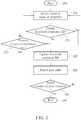
- FIG. 2is a diagram illustrating a flowchart of an example of operation of gain control circuit 110 as shown in FIG. 1 . Provided that substantially the same result is achieved, the steps of the flowchart shown in FIG. 2 need not be in the exact order shown and need not be contiguous, that is, other steps can be intermediate. Steps are detailed in the following:
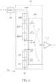
- FIG. 3is diagram illustrating an embodiment of the attenuation circuit 120 shown in FIG. 1 .
- the attenuation circuit 120comprises a programmable impedance element 1201 including impedance value Z1 that is programmable.
- the programmable impedance element 1201has one end connected between passive mixer 105 and amplifier 115 and has the other end connected to a ground level.
- the impedance of passive mixer 105is equal to ZMX, and the input impedance Zin of receiver front-end 100 depends on the impedance value Z1 and is equal to the sum of ZMX and Z1.
- the attenuation circuit 120for example comprises multiple programmable impedance elements.
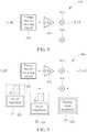
- FIG. 4is diagram illustrating another embodiment of the attenuation circuit 120 shown in FIG. 1 .
- the attenuation circuit 120comprises a first programmable impedance element 1202 and a second programmable impedance element 1203 that are connected in series.
- the programmable impedance elements 1202 and 1203include programmable impedance value Z2 and Z3, respectively.
- the programmable impedance element 1202has one end connected to the output of passive mixer 105 and has the other end connected to the input of amplifier 115, and the programmable impedance element 1203 has one end connected to the input of amplifier 115 and has the other end connected to the ground level.
- the impedance of passive mixer 105is equal to ZMX, and the input impedance Zin of receiver front-end 100 depends on the impedance value Z2+Z3 and is equal to the sum of ZMX, Z2, and Z3.
- the sum of impedance values Z2 and Z3can be configured as a constant and fixed value.
- the impedance value Z2is configured as A ⁇ Z0 and the impedance value Z3 is configured as (1-A) ⁇ Z0 wherein the parameter A is between zero and one and Z0 means a constant value.
- the input impedance Zin of receiver front-end 100can remain constant while multiple different gain settings are provided.
- FIG. 5is a diagram illustrating an example of programmable impedance ladder of the attenuation circuit 120 as shown in FIG. 1 .
- the attenuation circuit 120comprises a programmable impedance ladder 1204 including more impedance elements connected in series and a multiplexer switch 1205.
- the multiplexer switch 1205is arranged to select one gain setting among multiple different gain settings by selectively connecting the input of amplifier 115 to one node among the intermediate nodes (from n(1) to n(N-1)) based on the detection/control of detector 125 of FIG. 1 .
- Nmeans the total number of impedance elements in the programmable impedance ladder 1204, and Z(k) means the impedance value of k-th impedance element.
- Vomeans the voltage at input of the amplifier 115 (that is, the output voltage of passive mixer 105 after processed by the gain control circuit 120), Vi means input voltage of passive mixer 105, parameter s means that the multiplexer switch 1205 connects the input of amplifier 115 to the node between the s-th impedance element and the (s+1)-th impedance element.
- the impedance elementsare fixed values in FIG. 5 , it is not meant to be a limitation; in other embodiments, the impedance elements may have programmable impedance values, and similarly, the sum of impedance values of the total number of programmable impedance elements can be also configured as a constant and fixed value such that the input impedance Zin of receiver front-end 100 can remain constant while multiple different gain settings are provided.
- FIG. 6is block diagram illustrating a radio frequency (RF) receiver front-end 600 according to a second embodiment of the invention.
- the RF receiver front-end 600comprises a voltage step-up circuit 605, passive mixer 105, gain control circuit 110, and amplifier 115.
- the operations and functions of passive mixer 105, gain control circuit 110, and amplifier 115are identical to those circuit elements including the same reference numerals in FIG. 1 and are not detailed for brevity.
- the voltage step-up circuit 605comprising a transformer is used for receiving the high or radio frequency input signal S_RF to provide a voltage gain V5/V4 (that is equal to Z 5 Z 4 ) for the signal S RF wherein Z5 means impedance seen from voltage V5 to voltage step-up circuit 605 while Z4 means input impedance seen from voltage V4.
- the voltage step-up circuit 605is positioned preceding the passive mixer 105.
- the voltage gainis also referred as a step-up ratio.
- the voltage step-up circuit 605can be implemented by including an inductor L and a capacitor C without using a transformer.
- inductor L and capacitor Ccan be also used for providing the voltage gain V5/V4 (that is equal to Z 5 Z 4 ) for the signal S_RF.
- V5/V4that is equal to Z 5 Z 4
- a passive voltage gaincan be additionally obtained with low power consumption.
- FIG. 8is a block diagram of an RF receiver front-end 800 according to a first example, helpful to understand the invention.
- the RF receiver front-end 800is capable of supporting multiple gain modes to provide gain control for a high or radio frequency input signal S_RF to generate a low frequency signal S LF as well as providing better impedance matching capability with baseband circuit(s) or intermediate frequency circuit(s). Also, the receiver front-end 800 has lower input return loss and better/improved noise figure.
- Low frequency signal S_LFcan be a baseband signal or intermediate frequency signal.
- the receiver front-end 800comprises a voltage step-up circuit 805, at least one amplifier 810 such as an LNA, at least one first mixer 815, and at least one second mixer 820.
- the voltage step-up circuit 805is used for receiving a high or radio frequency input signal S_RF and providing a voltage gain (i.e. step-up ratio) for the input signal S_RF.
- the voltage step-up circuit 805can be implemented by using a transformer as shown in FIG. 6 or a combination of an inductor and a capacitor as shown in FIG. 7 .
- the LNA 810is coupled to the output of voltage step-up circuit 805 and to amplify the high or radio frequency input signal S_RF as well as reducing noise.
- the first mixer 815is coupled to the output of LNA 810 and is used for generating the low frequency signal S_LF in a first gain mode.
- the second mixer 820is coupled to the output of voltage step-up circuit 805 and is used for generating the low frequency signal S_LF in a gain mode (e.g. second gain mode) different from the first gain mode.
- the voltage step-up circuit 805, LNA 810, and first mixer 815are enabled in the first gain mode and configured to provide a first gain setting for the input signal S_RF to generate the low frequency signal S_LF. In the first gain mode, the second mixer 820 is disabled.
- the voltage step-up circuit 805 and second mixer 820are enabled and configured to provide a second gain setting for the input signal S_RF to generate the low frequency signal S_LF, and the LNA 810 and first mixer 815 are disabled.
- the voltage step-up circuit 805is enabled and employed in both the first and second gain modes. That is, the voltage step-up circuit 805 is shared by both the first mixer 815 and second mixer 820.
- the first gain modeis configured as a higher gain mode providing high gain setting for the signal S_RF to achieve lower noise with an acceptable linearity
- the second gain modeis configured as a low gain mode providing lower gain setting for the signal S RF to achieve a better linearity performance with acceptable noise.
- the RF receiver front-end 800can get a good trade-off between noise and linearity performance.
- utilizing the voltage step-up circuit 805can improve the total gain value of receiver front-end 800 by providing a passive voltage gain (i.e. step-up ratio). Both the above-mentioned gain modes share/use the same voltage step-up circuit 805 to provide multiple gain settings for the input signal S_RF.
- FIG. 9is a block diagram of an RF receiver front-end 900 according to a second example, helpful to understand the invention.
- the receiver front-end 900includes the capabilities of supporting multiple gain modes to provide gain control for the input signal S RF and providing better impedance matching with baseband circuit(s) or intermediate frequency circuit(s).
- the receiver 900comprises the voltage step-up circuit 805, the amplifier 810 such as LNA, first mixer 815, second mixer 820, first switchable impedance unit 825, second switchable impedance unit 830, and a variable impedance unit 835.
- the first switchable impedance unit 825comprises a switch S1 and a shunt impedance unit Z1
- the second switchable impedance unit 830comprises a switch S2 and a shunt impedance unit Z2.
- the variable impedance unit 835comprises a variable/programmable shunt impedance unit Z3.
- the receiver 900can support three different gain modes to provide three different gain settings for the input signal S_RF, and the voltage step-up circuit 810 is employed in all these three gain modes.
- the three gain modescomprise a high gain mode, a middle gain mode, and a low gain mode.
- the first mixer 815is coupled to the output of LNA 810 and is used for generating the low frequency signal S_LF in a high gain mode (this can be regarded as a first gain mode) .
- the second mixer 820is coupled to the output of voltage step-up circuit 805 and is used for generating the low frequency signal S_LF in middle and low gain modes (a second gain mode and a third gain mode) that are different from the high gain mode.
- the voltage step-up circuit 805, LNA 810, and first mixer 815are enabled in the high gain mode and configured to provide a high gain setting for the input signal S_RF to generate the low frequency signal S_LF.
- the second mixer 820is disabled, and the switches S1 and S2 are open (i.e. disabled) such that the shunt impedance units Z1 and Z2 are disconnected from the voltage step-up circuit 805.
- Voltage step-up circuit 805can provide a voltage gain for the input signal S_RF, and thus it is not required to configure/implement the LNA 810 with a higher gain value.
- the receiver 900is arranged to achieve better/excellent noise figure performance with an acceptable linearity performance; that is, the linearity performance can be secondary.
- variable shunt impedance unit Z3 of variable impedance unit 835is used for impedance matching and gain controls for the signal generate at the output of mixer 815 (i.e. the low frequency signal S_LF).
- the voltage step-up circuit 805 and second mixer 820are enabled and configured to provide a middle gain setting for the input signal S_RF to generate the low frequency signal S_LF.
- the LNA 810 and first mixer 815are disabled, and the switches S1 as well as S2 are open (i.e. disabled). Turning off the LNA 810 in the middle gain mode can reduce current consumption.
- the Voltage step-up circuit 805can provide a voltage gain for the input signal S_RF, and consequently the noise figure of the second mixer 820 can be significantly improved.
- the combination of a voltage step-up circuit and a passive mixerachieves an excellent linearity performance and good noise figure performance.
- the middle gain modeconsiders a trade-off between noise figure performance and linearity performance.
- the variable shunt impedance unit Z3 of variable impedance unit 835is used for impedance matching and gain controls for the signal generate at the output of mixer 820 (i.e. the low frequency signal S_LF).
- the voltage step-up circuit 805 and second mixer 820are enabled, and the switches S1 as well as S2 are closed (i.e. enabled).
- the LNA 810 and first mixer 815are disabled.
- the voltage step-up circuit 805, second mixer 820, and shunt impedance Z2are used for providing a low gain setting for the input signal S_RF to generate the low frequency signal S_LF.
- the switch S2is enabled to reduce the voltage gain (i.e. step-up ratio) provided by voltage step-up circuit 805 by shunting the input of second mixer 820 with the shunt impedance unit Z2.
- enabling the switch S1is to compensate the input return loss decreased by connecting the shunt impedance Z2 to the receiver front-end 900.
- the input return losscan be improved by shunting the input of voltage step-up circuit 805 with the shunt impedance unit Z1.
- the variable shunt impedance unit Z3 of variable impedance unit 835is used for impedance matching and gain controls for the signal generate at the output of mixer 820 (i.e. the low frequency signal S_LF).
- the first switchable impedance unit 825 and variable impedance unit 835can be excluded from the RF receiver front-end 900. That is, RF receiver front-end 900 can comprise only one switchable impedance unit 830 to provide middle gain setting. The first switchable impedance unit 825 and variable impedance unit 835 are optional.
- the voltage step-up circuit 805may be implemented by using the voltage step-up circuit 605 shown in FIG.6-FIG.7 (e.g. implemented by transformer, LC network or balun), the variable impedance unit 835 may be implemented by the gain control circuit 110 shown in FIG.1-FIG.7 , and the mixer 820 can be passive mixer. If the mixer 820 is implemented by a passive mixer, the variable impedance unit 835 can also be used to adjust the input return loss of the receiver front-end 900.
- FIG. 10shows a block diagram of an RF receiver front-end that combines the concepts of receiver front-end 100 and receiver front-end 900.
- the receiver front-end 1000provides impedance matching control and multiple gain modes for gain control while having low power consumption, good input return loss in all gain modes, and good noise figures in both high gain mode and middle gain mode. More specifically, the receiver front-end 1000 uses passive mixer 820 to save current consumption.
- the voltage step-up circuit 805 shared between all gain modesimproves noise figures and reduces power consumption as well.
- the switchable impedance unit 825 placed at RF input nodeimproves input return loss.
- the variable impedance unit 835 placed at mixer output nodeprovides impedance matching and additional gain control that ensures the linearity of the amplifier 115. No TIA is required, and the linearity of the receiver chain is maintained with low current consumption.
- the receiver front-end 1000is therefore suitable for low-power designs or ultra-low-power designs.
- an RF receiver front-endcan be configured to comprise a plurality of first mixers, a plurality of second mixers, a plurality of first switchable impedance units, and a plurality of second switchable impedance units wherein the plurality of first switchable impedance units can be optional (not limited).
- FIG. 11is a block diagram of an RF receiver front-end 1100 according to a third example, helpful to understand the invention.
- the receiver front-end 1100includes capabilities of supporting a variety of gain modes to provide gain control for the input signal S_RF and providing better impedance matching with baseband circuit(s) or intermediate frequency circuit(s).
- the receiver front-end 1100comprises the voltage step-up circuit 805, multiple amplifier 810A-810B such as LNA, multiple first mixers 815A-815B, multiple second mixers 820A-820B, multiple first switchable impedance units 825A-825B, multiple second switchable impedance units 830A-830B, and the variable impedance unit 835.
- the first switchable impedance units 825A and 825Bcomprise switches S1a-S1b and shunt impedance units Z1a-Z1b, respectively.
- the second switchable impedance units 830A-830Bcomprise switches S2a-S2b and shunt impedance units Z2a-Z2b, respectively.
- the variable impedance unit 835comprises the variable/programmable shunt impedance unit Z3.
- the impedance values of shunt impedance units Z1a-Z1b and shunt impedance units Z2a-Z2bare designed as different (but not limited).
- the receiver front-end 1100can support more than three different gain modes to provide more than three different gain settings for the input signal S_RF, and the voltage step-up circuit 810 is employed in all these gain modes. For each gain mode, only one among mixers 815A-815B and 820A-820B is enabled, and the other mixers are disabled. Each of switches S2a-S2b can be open or closed to connect or disconnect corresponding one of shunt impedance units Z2a-Z2b, respectively, to provide different gain settings in different gain modes.
- the switch S2a(or S2b) can be open or closed to connect or disconnect corresponding shunt impedance unit Z2a (or Z2b) to the mixer 820A, so as to provide different gain settings.
- the signal S_RFpasses through the voltage step-up circuit 805, the LNA 810A and the mixer 815A, and the low frequency signal S_LF is generated with a first gain; in a second gain mode, the signal S_RF passes through the voltage step-up circuit 805, the LNA 810B and the mixer 815B, and the low frequency signal S_LF is generated with a second gain; in a third gain mode, the signal S_RF passes through the voltage step-up circuit 805 and the mixer 820A, and the low frequency signal S_LF is generated with a third gain; in a fourth gain setting, the signal S_RF passes through the voltage step-up circuit 805 having the step-up ratio adjusted by the shunt impedance Z2a and the mixer 820A, and the low frequency signal S_LF is generated with a fourth gain; in a fifth gain setting, the signal S_RF passes through the voltage step-up circuit 805 having the step-up ratio adjusted by the shunt impedance Z2b and the
- the above operationis similar to second mixer 820B. Enabling one of the switches S2a-S2b can reduce the voltage gain (i.e. step-up ratio) provided by voltage step-up circuit 805 by shunting the input of second mixer 820 with one shunt impedance unit. In addition, enabling one of the switches S1a-S1b can improve input return loss by shunting the input of voltage step-up circuit 805 with one shunt impedance unit.
- first switchable impedance units 825A-825B and variable impedance unit 835can be excluded from the RF receiver front-end 1100. That is, RF receiver front-end 1100 can comprise only multiple second switchable impedance units 830A-830B to provide different gain settings. First switchable impedance units and variable impedance unit are optional. Additionally, the numbers of first switchable impedance units and second switchable impedance units are not limited. In other examples, more than two first switchable impedance units and more than two second switchable impedance units can be employed to provide more gain settings for the input signal S_RF.
- mixerscan be implemented by using single-sideband down-conversion mixers, single-balanced mixers, double-balanced mixers, I/Q down-conversion mixers, image-rejection down-conversion mixers, or any combinations.
Landscapes
- Engineering & Computer Science (AREA)
- Computer Networks & Wireless Communication (AREA)
- Signal Processing (AREA)
- Power Engineering (AREA)
- Circuits Of Receivers In General (AREA)
- Input Circuits Of Receivers And Coupling Of Receivers And Audio Equipment (AREA)
Description
- The present invention relates to a receiver scheme, and more particularly to a radio frequency (RF) receiver and RF receivers according to the pre-characterizing clauses of
claim 1. - The article "A 90nm CMOS Broadband Multi-Mode Mixed-Signal Demodulator for 60 GHz Radios", : XP011339636, by Kevin Chuang et. AL discloses a RF receiver according to the preamble portion of
claim 1. Further RF receivers are disclosed byJP2001044861A CN101064522A . - Generally speaking, a conventional receiver consists of a low-noise amplifier (LNA) for improving SNR, a mixer for frequency conversion, and a low-pass filter to filter out unwanted signals for channel selection. The linearity of the conventional receiver is usually limited by the LNA and mixer. To achieve high linearity, a conventional scheme may configure the output impedance of LNA to be a low impedance and pair with a passive mixer which has good linearity due to it passive nature. To achieve the low output impedance, the conventional scheme may employ a transimpedance amplifier (TIA) wherein the TIA has a low input impedance at baseband and this low input impedance can be frequency-translated to LNA output at RF frequency through the passive mixer. In addition, to suppress impairment introduced by a passive mixer, the mixer size has to be larger to minimize adding extra mixer switch impedance to the required low impedance path. Unfortunately, the larger mixer size requires larger LO drivers, and hence causes larger power consumption for the LO driver. The LO driver is the major power consumption contributor. In addition, for TIA to generate low impedance at its input, a large current consumption is required to maintain low noise and low impedance across the bandwidth. The TIA is another major power consumption contributor. It is a key issue to reduce larger power consumption from the LO driver and TIA for an ultra-lower power receiver design.
- Therefore one of the objectives of the present invention is to provide a receiver scheme having smaller LO driver(s) and TIA replaced configuration, to solve the above-mentioned problems.
- This is achieved by a radio frequency receiver according to
claim 1. The invention is defined inclaim 1. According to embodiments of the present invention, a radio frequency front-end receiver comprises a passive mixer, a gain control circuit, and an amplifier. The mixer is used for receiving a radio frequency signal and generating an output signal at a baseband frequency, and the output of the mixer is connected to a high impedance circuit. The gain control circuit is coupled between an output of the mixer and an input of the amplifier. The amplifier is coupled to the gain control circuit. The gain control circuit is arranged to detect a signal at the input of the amplifier to adjust a gain value that is exerted on the output signal generated at the output of the mixer to maintain linearity of the amplifier. - This document further discloses an RF receiver comprising a voltage step-up circuit, at least one amplifier, at least one first mixer, and at least one second mixer. The voltage step-up circuit is for receiving and providing a voltage gain for a radio frequency signal. The at least one amplifier is coupled to an output of the voltage step-up circuit. The at least one first mixer is coupled to an output of the at least one amplifier and used for generating the low frequency signal in a first gain mode. The at least one second mixer is coupled to the output of the voltage step-up circuit and used for generating the low frequency signal in a gain mode different from the first gain mode. The voltage step-up circuit, the amplifier, and the at least one first mixer are enabled in the first gain mode to generate the low frequency signal; the voltage step-up circuit and the at least one second mixer are enabled in the gain mode different from the first gain mode to generate the low frequency signal.
- This document further discloses an RF receiver. The RF receiver comprises an amplifier, a first mixer, a second mixer, and a switchable impedance unit. The amplifier is used for receiving and providing a voltage gain for a radio frequency input signal. The first mixer is coupled to an output of the amplifier. The second mixer is coupled to the input of the amplifier. The switchable impedance unit is selectively coupled to the second mixer. The amplifier and the first mixer are enabled in the first gain mode to generate the low frequency signal. The second mixer is enabled and the switchable impedance unit is not coupled to the second mixer in a second gain mode to generate the low frequency signal. The second mixer is enabled and the switchable impedance unit is coupled to the second mixer in a third gain mode to generate the low frequency signal. The first gain mode, the second gain mode, and the third gain mode respectively correspond to different gain settings
- In the following, the invention is further illustrated by way of example, taking reference to the accompanying drawings. Thereof
FIG. 1 is a block diagram of a radio frequency receiver front-end according to a first embodiment of the invention.FIG. 2 is a diagram illustrating a flowchart of an example of operation of gain control circuit as shown inFIG. 1 .FIG. 3 is a diagram illustrating an embodiment of the attenuation circuit as shown inFIG. 1 .FIG. 4 is a diagram illustrating another embodiment of the attenuation circuit as shown inFIG. 1 .FIG. 5 is a diagram illustrating an example of programmable impedance ladder of the attenuation circuit as shown inFIG. 1 .FIG. 6 is a block diagram illustrating a radio frequency receiver front-end according to a second embodiment of the invention.FIG. 7 is a block diagram illustrating another variation embodiment of a radio frequency receiver front-end according to the second embodiment shown inFIG. 6 .FIG. 8 is a block diagram of a radio frequency receiver front-end according to a first example.FIG. 9 is a block diagram of a radio frequency receiver front-end according to a second example.FIG. 10 shows a block diagram of an RF receiver front-end that combines the concepts of receiver front-end ofFIG. 1 and receiver front-end ofFIG. 9 .FIG. 11 is a block diagram of a radio frequency receiver front-end according to a third example.- For low-power or ultra-low-power receiver design(s), a passive mixer is preferred as it consumes less current. To reduce the size of passive mixer while keeping a high linearity and impedance matching of the receiver, the passive mixer is preferably to be a switch wherein the switch is with low impedance when enabled and is with high impedance when disabled. To achieve this, a passive mixer is usually to be large in device size to provide low impedance when enabled, and is usually used together with the TIA which has low output impedance. However, the cost of power consumption is high because of the large passive mixer and that the passive mixer is used with the TIA which has low output impedance.
- In embodiments of the invention, the objective is to (1) reduce power consumption, (2) make the input impedance and output impedance of passive mixer be configured as high impedances so that the receiver front-end can match with high input impedance of baseband circuits, and (3) maintain the linearity for making linearity performance be better than the linearity performance of the scheme employing the TIA having low output impedance.
- Please refer to
FIG. 1 , which is a block diagram of a radio frequency (RF) receiver front-end 100 according to a first embodiment of the invention. The receiver front-end 100 is able to fulfill the requirements of low power, high linearity, low noise, and good impedance matching, and can be employed in a low power (or ultra-low power) receiver architecture. The receiver front-end 100 can be applied to products based on the Internet of Things (IoT) technology. In addition, the receiver front-end 100 includes capabilities of gain control to provide different gain settings as well as impedance matching control. Specifically, the receiver front-end 100 is capable of matching with high input impedance of baseband circuits (or intermediate-frequency circuits) by using a mixer-first topology and is also capable of maintaining the high linearity of an amplifier in the open loop by the gain control capability so that no transimpedance amplifiers (TIA) are needed. In this embodiment, the receiver front-end 100 comprises apassive mixer 105, again control circuit 110, and anamplifier 115. Thepassive mixer 105 such as a voltage mode mixer or a current mode mixer is configured for converting the high or radio frequency input signal S_RF to generate the low frequency signal S_LF. The low frequency signal S_LF can be a baseband signal or an intermediate frequency signal. Thegain control circuit 110 is coupled between an output ofpassive mixer 105 and an input ofamplifier 115. Thegain control circuit 110 is arranged to detect a signal at the input ofamplifier 115 to adjust a gain value that is exerted on the low frequency signal S_LF generated at the output ofpassive mixer 105. In this embodiment, thegain control circuit 110 comprises anattenuation circuit 120 and adetector 125. Theattenuation circuit 120 is coupled between the output ofpassive mixer 105 and the input ofamplifier 115. Thedetector 125 is coupled to theattenuation circuit 120 and the input ofamplifier 115, and is used for sensing a level of the signal at the input ofamplifier 115 to control theattenuation circuit 120 to adjust/control the gain level to perform gain attenuation for a level of the low frequency signal S_LF. Thedetector 125 is arranged to compare the level of the signal at the input ofamplifier 115 with a threshold condition TH to determine whether to adjust the gain value. Theattenuation circuit 120 is arranged to provide multiple different gain settings. Accordingly, after the process of gain control/adjusting has been completed, the voltage swing at the input ofamplifier 115 does not exceed the threshold condition TH, which ensures that the linearity ofamplifier 115 will not be degraded. Note that theattenuation circuit 120 is also passive for linearity consideration, and thedetector 125 is a low-power fast detector as opposed to AGC with ADC which has long settling time. - By the architecture (mixer-first topology) of the receiver front-
end 100, the input impedance and output impedance ofpassive mixer 105 can be configured as high impedances so that the receiver front-end 100 can match with high input impedance of baseband circuits (or intermediate-frequency circuits). The circuit size ofpassive mixer 105 for implementation can be decreased to a smaller one. This achieves that even though a higher turned-on resistance Ron of transistors can still be tolerated as long as the output impedance of thepassive mixer 105 is greater than the turned-on resistance Ron. In addition, this makes a possibility to configure the gain value of an RF matching circuit as a higher value. Also, the forward transconductance gain can be configured to be a higher value since output thermal noise contribution becomes smaller due to that the receiver front-end 100 moderately matches with the high input impedance of baseband/intermediate-frequency circuits. - In addition, the
gain control circuit 110 is capable of gradually updating and changing (e.g., increasing, decreasing and remaining) thecircuit 110 gain value and the threshold condition TH that is used to be compared with the level of the signal at the input ofamplifier 115. The control can be implemented by analog circuit or digital circuit.. This improves the accuracy of gain control operation as well as maximizing the gain and noise performance without degrading the linearity of the receiver system.FIG. 2 is a diagram illustrating a flowchart of an example of operation ofgain control circuit 110 as shown inFIG. 1 . Provided that substantially the same result is achieved, the steps of the flowchart shown inFIG. 2 need not be in the exact order shown and need not be contiguous, that is, other steps can be intermediate. Steps are detailed in the following: - Step 205: Start;
- Step 210: Detect a signal at the input of
amplifier 115; - Step 215: determine whether to change the level of threshold condition TH or not. If it is determined to change the threshold condition TH, the flow proceeds to Step 220, otherwise, the flow proceeds to Step 225;
- Step 220: update the level of threshold condition TH;
- Step 225: decide if the process of gain control times out or not. If the gain control process times out, the flow proceeds to Step 240, otherwise, the flow proceeds to Step 210;
- Step 230: adjust the gain value that is exerted on the low frequency signal S_LF generated at the output of the
passive mixer 105; - Step 235: determine if the gain control process reaches the maximum gain iteration or not. If the gain control process reaches the maximum iteration, the flow proceeds to Step 240, otherwise, the flow proceeds to Step 210;
- Step 240: End.
- Further, in practice, the
attenuation circuit 120 for example equivalently comprises a programmable impedance element.FIG. 3 is diagram illustrating an embodiment of theattenuation circuit 120 shown inFIG. 1 . Theattenuation circuit 120 comprises aprogrammable impedance element 1201 including impedance value Z1 that is programmable. Theprogrammable impedance element 1201 has one end connected betweenpassive mixer 105 andamplifier 115 and has the other end connected to a ground level. The impedance ofpassive mixer 105 is equal to ZMX, and the input impedance Zin of receiver front-end 100 depends on the impedance value Z1 and is equal to the sum of ZMX and Z1. The gain value G ofpassive mixer 105 after adjusted by thegain control circuit 110 is determined by the following equation:
- In addition, in other embodiments, the
attenuation circuit 120 for example comprises multiple programmable impedance elements.FIG. 4 is diagram illustrating another embodiment of theattenuation circuit 120 shown inFIG. 1 . InFIG. 4 , theattenuation circuit 120 comprises a firstprogrammable impedance element 1202 and a secondprogrammable impedance element 1203 that are connected in series. Theprogrammable impedance elements programmable impedance element 1202 has one end connected to the output ofpassive mixer 105 and has the other end connected to the input ofamplifier 115, and theprogrammable impedance element 1203 has one end connected to the input ofamplifier 115 and has the other end connected to the ground level. The impedance ofpassive mixer 105 is equal to ZMX, and the input impedance Zin of receiver front-end 100 depends on the impedance value Z2+Z3 and is equal to the sum of ZMX, Z2, and Z3. The gain value G ofpassive mixer 105 after adjusted by thegain control circuit 110 is determined by the following equation:
- In this example, the sum of impedance values Z2 and Z3 can be configured as a constant and fixed value. For example, the impedance value Z2 is configured as A×Z0 and the impedance value Z3 is configured as (1-A)×Z0 wherein the parameter A is between zero and one and Z0 means a constant value. In this way, the input impedance Zin of receiver front-
end 100 can remain constant while multiple different gain settings are provided. FIG. 5 is a diagram illustrating an example of programmable impedance ladder of theattenuation circuit 120 as shown inFIG. 1 . InFIG. 5 , theattenuation circuit 120 comprises aprogrammable impedance ladder 1204 including more impedance elements connected in series and amultiplexer switch 1205. Themultiplexer switch 1205 is arranged to select one gain setting among multiple different gain settings by selectively connecting the input ofamplifier 115 to one node among the intermediate nodes (from n(1) to n(N-1)) based on the detection/control ofdetector 125 ofFIG. 1 . The impedance ofpassive mixer 105 is equal to ZMX, and the input impedance Zin of receiver front-end 100 is defined by the following equation:
- N means the total number of impedance elements in the
programmable impedance ladder 1204, and Z(k) means the impedance value of k-th impedance element. The gain value G ofpassive mixer 105 after adjusted by thegain control circuit 110 can be defined by the following equation:
- Vo means the voltage at input of the amplifier 115 (that is, the output voltage of
passive mixer 105 after processed by the gain control circuit 120), Vi means input voltage ofpassive mixer 105, parameter s means that themultiplexer switch 1205 connects the input ofamplifier 115 to the node between the s-th impedance element and the (s+1)-th impedance element. Although the impedance elements are fixed values inFIG. 5 , it is not meant to be a limitation; in other embodiments, the impedance elements may have programmable impedance values, and similarly, the sum of impedance values of the total number of programmable impedance elements can be also configured as a constant and fixed value such that the input impedance Zin of receiver front-end 100 can remain constant while multiple different gain settings are provided. - In addition, a voltage step-up circuit can be included within the above receiver.
FIG. 6 is block diagram illustrating a radio frequency (RF) receiver front-end 600 according to a second embodiment of the invention. The RF receiver front-end 600 comprises a voltage step-upcircuit 605,passive mixer 105, gaincontrol circuit 110, andamplifier 115. The operations and functions ofpassive mixer 105, gaincontrol circuit 110, andamplifier 115 are identical to those circuit elements including the same reference numerals inFIG. 1 and are not detailed for brevity. The voltage step-upcircuit 605 comprising a transformer is used for receiving the high or radio frequency input signal S_RF to provide a voltage gain V5/V4 (that is equal to
circuit 605 while Z4 means input impedance seen from voltage V4. The voltage step-upcircuit 605 is positioned preceding thepassive mixer 105. The voltage gain is also referred as a step-up ratio. Additionally, in other embodiments, as shown inFIG. 7 , the voltage step-upcircuit 605 can be implemented by including an inductor L and a capacitor C without using a transformer. The combination of inductor L and capacitor C can be also used for providing the voltage gain V5/V4 (that is equal to
circuit 605 at RF input node of the receiver front-end 600 (i.e., preceding thepassive mixer 105 in the mixer-first-and-high-baseband-input-impedance receiver topology), a passive voltage gain can be additionally obtained with low power consumption. FIG. 8 is a block diagram of an RF receiver front-end 800 according to a first example, helpful to understand the invention. The RF receiver front-end 800 is capable of supporting multiple gain modes to provide gain control for a high or radio frequency input signal S_RF to generate a low frequency signal S LF as well as providing better impedance matching capability with baseband circuit(s) or intermediate frequency circuit(s). Also, the receiver front-end 800 has lower input return loss and better/improved noise figure. Low frequency signal S_LF can be a baseband signal or intermediate frequency signal.- In this example, the receiver front-
end 800 comprises a voltage step-upcircuit 805, at least oneamplifier 810 such as an LNA, at least onefirst mixer 815, and at least onesecond mixer 820. The voltage step-upcircuit 805 is used for receiving a high or radio frequency input signal S_RF and providing a voltage gain (i.e. step-up ratio) for the input signal S_RF. The voltage step-upcircuit 805 can be implemented by using a transformer as shown inFIG. 6 or a combination of an inductor and a capacitor as shown inFIG. 7 . TheLNA 810 is coupled to the output of voltage step-upcircuit 805 and to amplify the high or radio frequency input signal S_RF as well as reducing noise. Thefirst mixer 815 is coupled to the output ofLNA 810 and is used for generating the low frequency signal S_LF in a first gain mode. Thesecond mixer 820 is coupled to the output of voltage step-upcircuit 805 and is used for generating the low frequency signal S_LF in a gain mode (e.g. second gain mode) different from the first gain mode. The voltage step-upcircuit 805,LNA 810, andfirst mixer 815 are enabled in the first gain mode and configured to provide a first gain setting for the input signal S_RF to generate the low frequency signal S_LF. In the first gain mode, thesecond mixer 820 is disabled. Additionally, in the second gain mode, the voltage step-upcircuit 805 andsecond mixer 820 are enabled and configured to provide a second gain setting for the input signal S_RF to generate the low frequency signal S_LF, and theLNA 810 andfirst mixer 815 are disabled. The voltage step-upcircuit 805 is enabled and employed in both the first and second gain modes. That is, the voltage step-upcircuit 805 is shared by both thefirst mixer 815 andsecond mixer 820. In this example, the first gain mode is configured as a higher gain mode providing high gain setting for the signal S_RF to achieve lower noise with an acceptable linearity, and the second gain mode is configured as a low gain mode providing lower gain setting for the signal S RF to achieve a better linearity performance with acceptable noise. The RF receiver front-end 800 can get a good trade-off between noise and linearity performance. In addition, utilizing the voltage step-upcircuit 805 can improve the total gain value of receiver front-end 800 by providing a passive voltage gain (i.e. step-up ratio). Both the above-mentioned gain modes share/use the same voltage step-upcircuit 805 to provide multiple gain settings for the input signal S_RF. - In another example, least one switchable impedance unit such as a combination of switch and shunt impedance unit can be added to an RF receiver front-end to further generate and provide a different gain setting for the input signal S RF.
FIG. 9 is a block diagram of an RF receiver front-end 900 according to a second example, helpful to understand the invention. The receiver front-end 900 includes the capabilities of supporting multiple gain modes to provide gain control for the input signal S RF and providing better impedance matching with baseband circuit(s) or intermediate frequency circuit(s). In practice, thereceiver 900 comprises the voltage step-upcircuit 805, theamplifier 810 such as LNA,first mixer 815,second mixer 820, firstswitchable impedance unit 825, secondswitchable impedance unit 830, and avariable impedance unit 835. The firstswitchable impedance unit 825 comprises a switch S1 and a shunt impedance unit Z1, and the secondswitchable impedance unit 830 comprises a switch S2 and a shunt impedance unit Z2. Thevariable impedance unit 835 comprises a variable/programmable shunt impedance unit Z3. - The
receiver 900 can support three different gain modes to provide three different gain settings for the input signal S_RF, and the voltage step-upcircuit 810 is employed in all these three gain modes. The three gain modes comprise a high gain mode, a middle gain mode, and a low gain mode. Thefirst mixer 815 is coupled to the output ofLNA 810 and is used for generating the low frequency signal S_LF in a high gain mode (this can be regarded as a first gain mode) . Thesecond mixer 820 is coupled to the output of voltage step-upcircuit 805 and is used for generating the low frequency signal S_LF in middle and low gain modes (a second gain mode and a third gain mode) that are different from the high gain mode. The voltage step-upcircuit 805,LNA 810, andfirst mixer 815 are enabled in the high gain mode and configured to provide a high gain setting for the input signal S_RF to generate the low frequency signal S_LF. In the high gain mode, thesecond mixer 820 is disabled, and the switches S1 and S2 are open (i.e. disabled) such that the shunt impedance units Z1 and Z2 are disconnected from the voltage step-upcircuit 805. Voltage step-upcircuit 805 can provide a voltage gain for the input signal S_RF, and thus it is not required to configure/implement theLNA 810 with a higher gain value. In the high gain mode, thereceiver 900 is arranged to achieve better/excellent noise figure performance with an acceptable linearity performance; that is, the linearity performance can be secondary. Current consumption ofLNA 810 can be reduced since of the operation of Voltage step-upcircuit 805 and that it is not required to make theLNA 810 support a higher gain value and a better linearity simultaneously. In addition, the variable shunt impedance unit Z3 ofvariable impedance unit 835 is used for impedance matching and gain controls for the signal generate at the output of mixer 815 (i.e. the low frequency signal S_LF). - Additionally, in the middle gain mode (second gain mode), the voltage step-up
circuit 805 andsecond mixer 820 are enabled and configured to provide a middle gain setting for the input signal S_RF to generate the low frequency signal S_LF. TheLNA 810 andfirst mixer 815 are disabled, and the switches S1 as well as S2 are open (i.e. disabled). Turning off theLNA 810 in the middle gain mode can reduce current consumption. The Voltage step-upcircuit 805 can provide a voltage gain for the input signal S_RF, and consequently the noise figure of thesecond mixer 820 can be significantly improved. The combination of a voltage step-up circuit and a passive mixer achieves an excellent linearity performance and good noise figure performance. The middle gain mode considers a trade-off between noise figure performance and linearity performance. In addition, the variable shunt impedance unit Z3 ofvariable impedance unit 835 is used for impedance matching and gain controls for the signal generate at the output of mixer 820 (i.e. the low frequency signal S_LF). - Additionally, in the low gain mode, the voltage step-up
circuit 805 andsecond mixer 820 are enabled, and the switches S1 as well as S2 are closed (i.e. enabled). TheLNA 810 andfirst mixer 815 are disabled. The voltage step-upcircuit 805,second mixer 820, and shunt impedance Z2 are used for providing a low gain setting for the input signal S_RF to generate the low frequency signal S_LF. In the low gain mode, the switch S2 is enabled to reduce the voltage gain (i.e. step-up ratio) provided by voltage step-upcircuit 805 by shunting the input ofsecond mixer 820 with the shunt impedance unit Z2. In addition, enabling the switch S1 is to compensate the input return loss decreased by connecting the shunt impedance Z2 to the receiver front-end 900. The input return loss can be improved by shunting the input of voltage step-upcircuit 805 with the shunt impedance unit Z1. In addition, the variable shunt impedance unit Z3 ofvariable impedance unit 835 is used for impedance matching and gain controls for the signal generate at the output of mixer 820 (i.e. the low frequency signal S_LF). - Further, in another example, the first
switchable impedance unit 825 andvariable impedance unit 835 can be excluded from the RF receiver front-end 900. That is, RF receiver front-end 900 can comprise only oneswitchable impedance unit 830 to provide middle gain setting. The firstswitchable impedance unit 825 andvariable impedance unit 835 are optional. - It should be appreciated by a skilled person after reading the above descriptions that the voltage step-up
circuit 805 may be implemented by using the voltage step-upcircuit 605 shown inFIG.6-FIG.7 (e.g. implemented by transformer, LC network or balun), thevariable impedance unit 835 may be implemented by thegain control circuit 110 shown inFIG.1-FIG.7 , and themixer 820 can be passive mixer. If themixer 820 is implemented by a passive mixer, thevariable impedance unit 835 can also be used to adjust the input return loss of the receiver front-end 900.FIG. 10 shows a block diagram of an RF receiver front-end that combines the concepts of receiver front-end 100 and receiver front-end 900. The receiver front-end 1000 provides impedance matching control and multiple gain modes for gain control while having low power consumption, good input return loss in all gain modes, and good noise figures in both high gain mode and middle gain mode. More specifically, the receiver front-end 1000 usespassive mixer 820 to save current consumption. The voltage step-upcircuit 805 shared between all gain modes improves noise figures and reduces power consumption as well. Theswitchable impedance unit 825 placed at RF input node improves input return loss. Thevariable impedance unit 835 placed at mixer output node provides impedance matching and additional gain control that ensures the linearity of theamplifier 115. No TIA is required, and the linearity of the receiver chain is maintained with low current consumption. The receiver front-end 1000 is therefore suitable for low-power designs or ultra-low-power designs. - Further, in another example, an RF receiver front-end can be configured to comprise a plurality of first mixers, a plurality of second mixers, a plurality of first switchable impedance units, and a plurality of second switchable impedance units wherein the plurality of first switchable impedance units can be optional (not limited).
FIG. 11 is a block diagram of an RF receiver front-end 1100 according to a third example, helpful to understand the invention. The receiver front-end 1100 includes capabilities of supporting a variety of gain modes to provide gain control for the input signal S_RF and providing better impedance matching with baseband circuit(s) or intermediate frequency circuit(s). In practice, the receiver front-end 1100 comprises the voltage step-upcircuit 805,multiple amplifier 810A-810B such as LNA, multiplefirst mixers 815A-815B, multiplesecond mixers 820A-820B, multiple firstswitchable impedance units 825A-825B, multiple secondswitchable impedance units 830A-830B, and thevariable impedance unit 835. The firstswitchable impedance units switchable impedance units 830A-830B comprise switches S2a-S2b and shunt impedance units Z2a-Z2b, respectively. Thevariable impedance unit 835 comprises the variable/programmable shunt impedance unit Z3. The impedance values of shunt impedance units Z1a-Z1b and shunt impedance units Z2a-Z2b are designed as different (but not limited). - The receiver front-
end 1100 can support more than three different gain modes to provide more than three different gain settings for the input signal S_RF, and the voltage step-upcircuit 810 is employed in all these gain modes. For each gain mode, only one amongmixers 815A-815B and 820A-820B is enabled, and the other mixers are disabled. Each of switches S2a-S2b can be open or closed to connect or disconnect corresponding one of shunt impedance units Z2a-Z2b, respectively, to provide different gain settings in different gain modes. For example, when thesecond mixer 820A is enabled, the switch S2a (or S2b) can be open or closed to connect or disconnect corresponding shunt impedance unit Z2a (or Z2b) to themixer 820A, so as to provide different gain settings. For example, in a first gain mode, the signal S_RF passes through the voltage step-upcircuit 805, theLNA 810A and themixer 815A, and the low frequency signal S_LF is generated with a first gain; in a second gain mode, the signal S_RF passes through the voltage step-upcircuit 805, theLNA 810B and themixer 815B, and the low frequency signal S_LF is generated with a second gain; in a third gain mode, the signal S_RF passes through the voltage step-upcircuit 805 and themixer 820A, and the low frequency signal S_LF is generated with a third gain; in a fourth gain setting, the signal S_RF passes through the voltage step-upcircuit 805 having the step-up ratio adjusted by the shunt impedance Z2a and themixer 820A, and the low frequency signal S_LF is generated with a fourth gain; in a fifth gain setting, the signal S_RF passes through the voltage step-upcircuit 805 having the step-up ratio adjusted by the shunt impedance Z2b and themixer 820A, and the low frequency signal S_LF is generated with a fifth gain, and the rest can be deduced by analogy. The above operation is similar tosecond mixer 820B. Enabling one of the switches S2a-S2b can reduce the voltage gain (i.e. step-up ratio) provided by voltage step-upcircuit 805 by shunting the input ofsecond mixer 820 with one shunt impedance unit. In addition, enabling one of the switches S1a-S1b can improve input return loss by shunting the input of voltage step-upcircuit 805 with one shunt impedance unit. - Further, in another example, the first
switchable impedance units 825A-825B andvariable impedance unit 835 can be excluded from the RF receiver front-end 1100. That is, RF receiver front-end 1100 can comprise only multiple secondswitchable impedance units 830A-830B to provide different gain settings. First switchable impedance units and variable impedance unit are optional. Additionally, the numbers of first switchable impedance units and second switchable impedance units are not limited. In other examples, more than two first switchable impedance units and more than two second switchable impedance units can be employed to provide more gain settings for the input signal S_RF. Furthermore, it should be noted that the above-mentioned mixers can be implemented by using single-sideband down-conversion mixers, single-balanced mixers, double-balanced mixers, I/Q down-conversion mixers, image-rejection down-conversion mixers, or any combinations.


Claims (5)
- A radio frequency, RF, receiver, comprising a receiver front-end (100, 600), the receiver front-end (100, 600) comprising:a passive mixer (105), having an input for receiving a radio frequency signal and an output for generating an output signal at a baseband : frequency or an intermediate frequency, wherein the input impedance and output impedance of the passive mixer (105) are configured as high impedances so that the receiver front-end (100, 600) matches with a high impedance of baseband circuits and intermediate-frequency circuits, respectively;a gain control circuit (110), coupled between the output of the passive mixer (105) and an input of an amplifier (115); and the amplifier (115), coupled to the gain control circuit (110);wherein the gain control circuit (110) is arranged to detect a signal at the input of the amplifier (115) to adjust a gain value that is exerted on the output signal generated at the output of the passive mixer (105) to maintain linearity of the amplifier (115),characterized in that the gain control circuit (110) comprises:a passive attenuation circuit (120), coupled between the output of the passive mixer (105) and the input of the amplifier (115); anda detector (125), coupled to the passive attenuation circuit (120) and the input of the amplifier (115), for sensing a level of the signal at the input of the amplifier (115), and sending a control signal to control the passive attenuation circuit (120) to adjust the gain level to perform gain attenuation for a level of the output signal generated at the output of the passive mixer (105).
- The receiver of claim 1,characterized in that the detector (125) is arranged to compare the level of the signal at the input of the amplifier (115) with a threshold condition to determine whether to adjust the gain value.
- The receiver of claim 1,characterized in:that the passive attenuation circuit (120) comprises a programmable impedance element (1201) having one end connected between the passive mixer (105) and the amplifier (115), the programmable impedance element (1201) includes a programmable impedance value Z1; orthe passive attenuation circuit (120) comprises a first programmable impedance element (1202) and a second programmable impedance element (1203) connected in series; the input of the amplifier (115) is connected between the first and second programmable impedance elements (1202, 1203); the first programmable impedance element (1202) includes a programmable impedance value Z2, and the second programmable impedance element (1203) includes a programmable impedance value Z3, a sum of Z2 and Z3 being constant.
- The receiver of claim 1,characterized in that the passive attenuation circuit (120) comprises:a multiplexer switch (1205); andan impedance ladder (1204) including a plurality of impedance elements connected in series and including a plurality of nodes which are selectively connected to the multiplexer switch (1205);wherein the multiplexer switch (1205) is arranged to connect the input of the amplifier (115) to one node among the plurality of nodes according to a control of the detector (125), to provide a gain setting.
- The receiver of claim 1, furthercharacterized by:
a voltage step-up circuit (605), coupled to the input of the passive mixer (105), for receiving and providing a voltage gain for the radio frequency signal.
Priority Applications (1)
| Application Number | Priority Date | Filing Date | Title |
|---|---|---|---|
| EP21150080.6AEP3826178A1 (en) | 2015-09-08 | 2016-09-08 | Radio frequency receiver front-end with gain control capability as well as improved impedance matching control capability |
Applications Claiming Priority (2)
| Application Number | Priority Date | Filing Date | Title |
|---|---|---|---|
| US201562215284P | 2015-09-08 | 2015-09-08 | |
| US15/256,730US9748993B2 (en) | 2015-09-08 | 2016-09-05 | Radio frequency receiver front-end with gain control capability as well as improved impedance matching control capability |
Related Child Applications (2)
| Application Number | Title | Priority Date | Filing Date |
|---|---|---|---|
| EP21150080.6ADivision-IntoEP3826178A1 (en) | 2015-09-08 | 2016-09-08 | Radio frequency receiver front-end with gain control capability as well as improved impedance matching control capability |
| EP21150080.6ADivisionEP3826178A1 (en) | 2015-09-08 | 2016-09-08 | Radio frequency receiver front-end with gain control capability as well as improved impedance matching control capability |
Publications (3)
| Publication Number | Publication Date |
|---|---|
| EP3142254A2 EP3142254A2 (en) | 2017-03-15 |
| EP3142254A3 EP3142254A3 (en) | 2017-06-21 |
| EP3142254B1true EP3142254B1 (en) | 2021-02-17 |
Family
ID=56920520
Family Applications (2)
| Application Number | Title | Priority Date | Filing Date |
|---|---|---|---|
| EP21150080.6APendingEP3826178A1 (en) | 2015-09-08 | 2016-09-08 | Radio frequency receiver front-end with gain control capability as well as improved impedance matching control capability |
| EP16187749.3AActiveEP3142254B1 (en) | 2015-09-08 | 2016-09-08 | Radio frequency receiver front-end with gain control capability as well as improved impedance matching control capability |
Family Applications Before (1)
| Application Number | Title | Priority Date | Filing Date |
|---|---|---|---|
| EP21150080.6APendingEP3826178A1 (en) | 2015-09-08 | 2016-09-08 | Radio frequency receiver front-end with gain control capability as well as improved impedance matching control capability |
Country Status (3)
| Country | Link |
|---|---|
| US (1) | US9748993B2 (en) |
| EP (2) | EP3826178A1 (en) |
| CN (1) | CN106992795B (en) |
Families Citing this family (14)
| Publication number | Priority date | Publication date | Assignee | Title |
|---|---|---|---|---|
| KR102552581B1 (en)* | 2016-08-30 | 2023-07-07 | 스카이워크스 솔루션즈, 인코포레이티드 | Multi-Input Amplifier with Programmable Embedded Attenuators |
| US9941849B1 (en) | 2017-02-10 | 2018-04-10 | Psemi Corporation | Programmable optimized band switching LNA for operation in multiple narrow-band frequency ranges |
| US11881828B2 (en) | 2017-04-04 | 2024-01-23 | Psemi Corporation | Tunable effective inductance for multi-gain LNA with inductive source degeneration |
| US10038418B1 (en) | 2017-04-04 | 2018-07-31 | Psemi Corporation | Optimized multi gain LNA enabling low current and high linearity including highly linear active bypass |
| US20200007098A1 (en)* | 2018-06-29 | 2020-01-02 | Qualcomm Incorporated | Dual-Mode Amplification by Varying a Load Impedance |
| CN111162809B (en)* | 2019-12-13 | 2022-04-15 | 西安易朴通讯技术有限公司 | Wireless receiver and wireless device |
| CN112511179B (en)* | 2020-11-02 | 2022-03-22 | 扬州船用电子仪器研究所(中国船舶重工集团公司第七二三研究所) | Reconfigurable radio frequency front-end receiving circuit |
| US11277109B1 (en)* | 2021-02-09 | 2022-03-15 | Psemi Corporation | Disabled input switch for LNA input attenuation |
| FR3120279B1 (en)* | 2021-02-26 | 2024-01-05 | St Microelectronics Grenoble 2 | Calibration of an RF attenuator |
| CN113556090A (en)* | 2021-07-28 | 2021-10-26 | 深圳昂瑞微电子技术有限公司 | Linearity optimization circuit and low noise amplifier including the same |
| US11539347B1 (en)* | 2021-09-03 | 2022-12-27 | International Business Machines Corporation | Current-mode frequency translation circuit with programmable gain |
| CN113992234B (en)* | 2021-12-27 | 2022-03-25 | 智道网联科技(北京)有限公司 | Circuit for vehicle V2X device, vehicle V2X device and vehicle |
| CN218633923U (en)* | 2022-11-07 | 2023-03-14 | 深圳飞骧科技股份有限公司 | Passive circuit under radio frequency receiving module bypass mode and radio frequency receiving module |
| CN116015331B (en)* | 2022-12-26 | 2023-08-08 | 成都爱科特科技发展有限公司 | Complex electromagnetic environment weak signal receiving method, device and system |
Family Cites Families (12)
| Publication number | Priority date | Publication date | Assignee | Title |
|---|---|---|---|---|
| JP2001044861A (en) | 1999-07-27 | 2001-02-16 | Kyocera Corp | Receiver |
| US6639447B2 (en)* | 2002-03-08 | 2003-10-28 | Sirific Wireless Corporation | High linearity Gilbert I Q dual mixer |
| CN100517993C (en) | 2006-04-24 | 2009-07-22 | 中兴通讯股份有限公司 | A Multifunctional Transceiver Used in Time Division Duplex System |
| US8600300B2 (en)* | 2006-12-06 | 2013-12-03 | Broadcom Corporation | Method and system for single chip WLAN and bluetooth radios on a single CMOS substrate |
| US7599675B2 (en)* | 2006-12-12 | 2009-10-06 | Telefonaktiebolaget Lm Ericsson (Publ) | Method and apparatus for receiving radio frequency signals |
| CN101641929A (en)* | 2007-01-26 | 2010-02-03 | 新加坡科技研究局 | A radio frequency indentification transceiver |
| US8639205B2 (en) | 2008-03-20 | 2014-01-28 | Qualcomm Incorporated | Reduced power-consumption receivers |
| US8433272B2 (en)* | 2008-04-15 | 2013-04-30 | Qualcomm Incorporated | Reconfigurable high linearity low noise figure receiver requiring no interstage saw filter |
| US8351978B2 (en)* | 2008-08-01 | 2013-01-08 | Aleksandar Tasic | Systems and methods for adjusting the gain of a receiver through a gain tuning network |
| US8086208B2 (en) | 2008-12-05 | 2011-12-27 | Passif Semiconductor Corp. | Passive wireless receiver |
| CN102664653B (en)* | 2012-05-17 | 2014-09-03 | 天津里外科技有限公司 | Mobile terminal and radio frequency front terminal thereof with radio frequency digital-to-analog conversion type linear transmitter |
| US9548709B2 (en) | 2012-12-19 | 2017-01-17 | Qualcomm Incorporated | Independent gain control for multiple receive circuits concurrently processing different transmitted signals |
- 2016
- 2016-09-05USUS15/256,730patent/US9748993B2/enactiveActive
- 2016-09-08EPEP21150080.6Apatent/EP3826178A1/enactivePending
- 2016-09-08EPEP16187749.3Apatent/EP3142254B1/enactiveActive
- 2016-09-08CNCN201610810277.XApatent/CN106992795B/enactiveActive
Non-Patent Citations (1)
| Title |
|---|
| None* |
Also Published As
| Publication number | Publication date |
|---|---|
| CN106992795B (en) | 2019-04-26 |
| US9748993B2 (en) | 2017-08-29 |
| EP3826178A1 (en) | 2021-05-26 |
| US20170070252A1 (en) | 2017-03-09 |
| EP3142254A2 (en) | 2017-03-15 |
| CN106992795A (en) | 2017-07-28 |
| EP3142254A3 (en) | 2017-06-21 |
Similar Documents
| Publication | Publication Date | Title |
|---|---|---|
| EP3142254B1 (en) | Radio frequency receiver front-end with gain control capability as well as improved impedance matching control capability | |
| US10205438B2 (en) | Adjustable low-pass filter in a compact low-power receiver | |
| US10193583B2 (en) | Radio frequency tuner | |
| US9166632B1 (en) | Mixer circuits with programmable characteristics | |
| US8331895B2 (en) | Receiving circuit | |
| WO2009058912A1 (en) | Degenerated passive mixer in saw-less receiver | |
| US9496906B2 (en) | Receiver with wide gain range | |
| JPWO2014080586A1 (en) | Variable gain amplifier and tuner system including the same | |
| EP3278459A1 (en) | Receiving a plurality of radio frequency bands | |
| US20060164164A1 (en) | Variable gain amplifier with low phase variation | |
| KR100882406B1 (en) | Reconfigurable Frequency Filter | |
| US8816750B2 (en) | High frequency mixer with tunable dynamic range | |
| US9525447B1 (en) | Radio receiver co-existence | |
| WO2015019525A1 (en) | Cascode-type transconductance amplifier and variable gain circuit, and tuner system provided with same | |
| EP1608061A1 (en) | Frequency converter using a tunable bandpass filter | |
| JP2001028553A (en) | Radio apparatus and gain control method | |
| CN114978062A (en) | Low noise amplifier and receiving circuit | |
| HK1116935B (en) | Transconductance circuit module and radio frequency filter |
Legal Events
| Date | Code | Title | Description |
|---|---|---|---|
| PUAI | Public reference made under article 153(3) epc to a published international application that has entered the european phase | Free format text:ORIGINAL CODE: 0009012 | |
| STAA | Information on the status of an ep patent application or granted ep patent | Free format text:STATUS: THE APPLICATION HAS BEEN PUBLISHED | |
| AK | Designated contracting states | Kind code of ref document:A2 Designated state(s):AL AT BE BG CH CY CZ DE DK EE ES FI FR GB GR HR HU IE IS IT LI LT LU LV MC MK MT NL NO PL PT RO RS SE SI SK SM TR | |
| AX | Request for extension of the european patent | Extension state:BA ME | |
| PUAL | Search report despatched | Free format text:ORIGINAL CODE: 0009013 | |
| AK | Designated contracting states | Kind code of ref document:A3 Designated state(s):AL AT BE BG CH CY CZ DE DK EE ES FI FR GB GR HR HU IE IS IT LI LT LU LV MC MK MT NL NO PL PT RO RS SE SI SK SM TR | |
| AX | Request for extension of the european patent | Extension state:BA ME | |
| RIC1 | Information provided on ipc code assigned before grant | Ipc:H04B 1/30 20060101ALI20170515BHEP Ipc:H03G 3/30 20060101AFI20170515BHEP | |
| STAA | Information on the status of an ep patent application or granted ep patent | Free format text:STATUS: REQUEST FOR EXAMINATION WAS MADE | |
| 17P | Request for examination filed | Effective date:20171219 | |
| RBV | Designated contracting states (corrected) | Designated state(s):AL AT BE BG CH CY CZ DE DK EE ES FI FR GB GR HR HU IE IS IT LI LT LU LV MC MK MT NL NO PL PT RO RS SE SI SK SM TR | |
| STAA | Information on the status of an ep patent application or granted ep patent | Free format text:STATUS: EXAMINATION IS IN PROGRESS | |
| 17Q | First examination report despatched | Effective date:20191121 | |
| RIC1 | Information provided on ipc code assigned before grant | Ipc:H04B 1/30 20060101ALI20200731BHEP Ipc:H03D 7/14 20060101ALI20200731BHEP Ipc:H03G 3/30 20060101AFI20200731BHEP Ipc:H04B 1/16 20060101ALI20200731BHEP Ipc:H04B 1/40 20150101ALI20200731BHEP | |
| GRAP | Despatch of communication of intention to grant a patent | Free format text:ORIGINAL CODE: EPIDOSNIGR1 | |
| STAA | Information on the status of an ep patent application or granted ep patent | Free format text:STATUS: GRANT OF PATENT IS INTENDED | |
| INTG | Intention to grant announced | Effective date:20200911 | |
| GRAS | Grant fee paid | Free format text:ORIGINAL CODE: EPIDOSNIGR3 | |
| GRAA | (expected) grant | Free format text:ORIGINAL CODE: 0009210 | |
| STAA | Information on the status of an ep patent application or granted ep patent | Free format text:STATUS: THE PATENT HAS BEEN GRANTED | |
| AK | Designated contracting states | Kind code of ref document:B1 Designated state(s):AL AT BE BG CH CY CZ DE DK EE ES FI FR GB GR HR HU IE IS IT LI LT LU LV MC MK MT NL NO PL PT RO RS SE SI SK SM TR | |
| REG | Reference to a national code | Ref country code:GB Ref legal event code:FG4D | |
| REG | Reference to a national code | Ref country code:CH Ref legal event code:EP | |
| REG | Reference to a national code | Ref country code:DE Ref legal event code:R096 Ref document number:602016052486 Country of ref document:DE | |
| REG | Reference to a national code | Ref country code:AT Ref legal event code:REF Ref document number:1362837 Country of ref document:AT Kind code of ref document:T Effective date:20210315 | |
| REG | Reference to a national code | Ref country code:IE Ref legal event code:FG4D | |
| REG | Reference to a national code | Ref country code:LT Ref legal event code:MG9D | |
| REG | Reference to a national code | Ref country code:NL Ref legal event code:MP Effective date:20210217 | |
| PG25 | Lapsed in a contracting state [announced via postgrant information from national office to epo] | Ref country code:PT Free format text:LAPSE BECAUSE OF FAILURE TO SUBMIT A TRANSLATION OF THE DESCRIPTION OR TO PAY THE FEE WITHIN THE PRESCRIBED TIME-LIMIT Effective date:20210617 Ref country code:NO Free format text:LAPSE BECAUSE OF FAILURE TO SUBMIT A TRANSLATION OF THE DESCRIPTION OR TO PAY THE FEE WITHIN THE PRESCRIBED TIME-LIMIT Effective date:20210517 Ref country code:LT Free format text:LAPSE BECAUSE OF FAILURE TO SUBMIT A TRANSLATION OF THE DESCRIPTION OR TO PAY THE FEE WITHIN THE PRESCRIBED TIME-LIMIT Effective date:20210217 Ref country code:FI Free format text:LAPSE BECAUSE OF FAILURE TO SUBMIT A TRANSLATION OF THE DESCRIPTION OR TO PAY THE FEE WITHIN THE PRESCRIBED TIME-LIMIT Effective date:20210217 Ref country code:GR Free format text:LAPSE BECAUSE OF FAILURE TO SUBMIT A TRANSLATION OF THE DESCRIPTION OR TO PAY THE FEE WITHIN THE PRESCRIBED TIME-LIMIT Effective date:20210518 Ref country code:HR Free format text:LAPSE BECAUSE OF FAILURE TO SUBMIT A TRANSLATION OF THE DESCRIPTION OR TO PAY THE FEE WITHIN THE PRESCRIBED TIME-LIMIT Effective date:20210217 Ref country code:BG Free format text:LAPSE BECAUSE OF FAILURE TO SUBMIT A TRANSLATION OF THE DESCRIPTION OR TO PAY THE FEE WITHIN THE PRESCRIBED TIME-LIMIT Effective date:20210517 | |
| REG | Reference to a national code | Ref country code:AT Ref legal event code:MK05 Ref document number:1362837 Country of ref document:AT Kind code of ref document:T Effective date:20210217 | |
| PG25 | Lapsed in a contracting state [announced via postgrant information from national office to epo] | Ref country code:SE Free format text:LAPSE BECAUSE OF FAILURE TO SUBMIT A TRANSLATION OF THE DESCRIPTION OR TO PAY THE FEE WITHIN THE PRESCRIBED TIME-LIMIT Effective date:20210217 Ref country code:NL Free format text:LAPSE BECAUSE OF FAILURE TO SUBMIT A TRANSLATION OF THE DESCRIPTION OR TO PAY THE FEE WITHIN THE PRESCRIBED TIME-LIMIT Effective date:20210217 Ref country code:LV Free format text:LAPSE BECAUSE OF FAILURE TO SUBMIT A TRANSLATION OF THE DESCRIPTION OR TO PAY THE FEE WITHIN THE PRESCRIBED TIME-LIMIT Effective date:20210217 Ref country code:RS Free format text:LAPSE BECAUSE OF FAILURE TO SUBMIT A TRANSLATION OF THE DESCRIPTION OR TO PAY THE FEE WITHIN THE PRESCRIBED TIME-LIMIT Effective date:20210217 Ref country code:PL Free format text:LAPSE BECAUSE OF FAILURE TO SUBMIT A TRANSLATION OF THE DESCRIPTION OR TO PAY THE FEE WITHIN THE PRESCRIBED TIME-LIMIT Effective date:20210217 | |
| PG25 | Lapsed in a contracting state [announced via postgrant information from national office to epo] | Ref country code:IS Free format text:LAPSE BECAUSE OF FAILURE TO SUBMIT A TRANSLATION OF THE DESCRIPTION OR TO PAY THE FEE WITHIN THE PRESCRIBED TIME-LIMIT Effective date:20210617 | |
| PG25 | Lapsed in a contracting state [announced via postgrant information from national office to epo] | Ref country code:EE Free format text:LAPSE BECAUSE OF FAILURE TO SUBMIT A TRANSLATION OF THE DESCRIPTION OR TO PAY THE FEE WITHIN THE PRESCRIBED TIME-LIMIT Effective date:20210217 Ref country code:CZ Free format text:LAPSE BECAUSE OF FAILURE TO SUBMIT A TRANSLATION OF THE DESCRIPTION OR TO PAY THE FEE WITHIN THE PRESCRIBED TIME-LIMIT Effective date:20210217 Ref country code:AT Free format text:LAPSE BECAUSE OF FAILURE TO SUBMIT A TRANSLATION OF THE DESCRIPTION OR TO PAY THE FEE WITHIN THE PRESCRIBED TIME-LIMIT Effective date:20210217 Ref country code:SM Free format text:LAPSE BECAUSE OF FAILURE TO SUBMIT A TRANSLATION OF THE DESCRIPTION OR TO PAY THE FEE WITHIN THE PRESCRIBED TIME-LIMIT Effective date:20210217 | |
| REG | Reference to a national code | Ref country code:DE Ref legal event code:R097 Ref document number:602016052486 Country of ref document:DE | |
| PG25 | Lapsed in a contracting state [announced via postgrant information from national office to epo] | Ref country code:ES Free format text:LAPSE BECAUSE OF FAILURE TO SUBMIT A TRANSLATION OF THE DESCRIPTION OR TO PAY THE FEE WITHIN THE PRESCRIBED TIME-LIMIT Effective date:20210217 Ref country code:DK Free format text:LAPSE BECAUSE OF FAILURE TO SUBMIT A TRANSLATION OF THE DESCRIPTION OR TO PAY THE FEE WITHIN THE PRESCRIBED TIME-LIMIT Effective date:20210217 Ref country code:SK Free format text:LAPSE BECAUSE OF FAILURE TO SUBMIT A TRANSLATION OF THE DESCRIPTION OR TO PAY THE FEE WITHIN THE PRESCRIBED TIME-LIMIT Effective date:20210217 Ref country code:RO Free format text:LAPSE BECAUSE OF FAILURE TO SUBMIT A TRANSLATION OF THE DESCRIPTION OR TO PAY THE FEE WITHIN THE PRESCRIBED TIME-LIMIT Effective date:20210217 | |
| PLBE | No opposition filed within time limit | Free format text:ORIGINAL CODE: 0009261 | |
| STAA | Information on the status of an ep patent application or granted ep patent | Free format text:STATUS: NO OPPOSITION FILED WITHIN TIME LIMIT | |
| 26N | No opposition filed | Effective date:20211118 | |
| PG25 | Lapsed in a contracting state [announced via postgrant information from national office to epo] | Ref country code:AL Free format text:LAPSE BECAUSE OF FAILURE TO SUBMIT A TRANSLATION OF THE DESCRIPTION OR TO PAY THE FEE WITHIN THE PRESCRIBED TIME-LIMIT Effective date:20210217 | |
| PG25 | Lapsed in a contracting state [announced via postgrant information from national office to epo] | Ref country code:SI Free format text:LAPSE BECAUSE OF FAILURE TO SUBMIT A TRANSLATION OF THE DESCRIPTION OR TO PAY THE FEE WITHIN THE PRESCRIBED TIME-LIMIT Effective date:20210217 | |
| PG25 | Lapsed in a contracting state [announced via postgrant information from national office to epo] | Ref country code:IT Free format text:LAPSE BECAUSE OF FAILURE TO SUBMIT A TRANSLATION OF THE DESCRIPTION OR TO PAY THE FEE WITHIN THE PRESCRIBED TIME-LIMIT Effective date:20210217 | |
| REG | Reference to a national code | Ref country code:CH Ref legal event code:PL | |
| REG | Reference to a national code | Ref country code:BE Ref legal event code:MM Effective date:20210930 | |
| PG25 | Lapsed in a contracting state [announced via postgrant information from national office to epo] | Ref country code:IS Free format text:LAPSE BECAUSE OF FAILURE TO SUBMIT A TRANSLATION OF THE DESCRIPTION OR TO PAY THE FEE WITHIN THE PRESCRIBED TIME-LIMIT Effective date:20210617 Ref country code:MC Free format text:LAPSE BECAUSE OF FAILURE TO SUBMIT A TRANSLATION OF THE DESCRIPTION OR TO PAY THE FEE WITHIN THE PRESCRIBED TIME-LIMIT Effective date:20210217 | |
| PG25 | Lapsed in a contracting state [announced via postgrant information from national office to epo] | Ref country code:LU Free format text:LAPSE BECAUSE OF NON-PAYMENT OF DUE FEES Effective date:20210908 Ref country code:IE Free format text:LAPSE BECAUSE OF NON-PAYMENT OF DUE FEES Effective date:20210908 Ref country code:BE Free format text:LAPSE BECAUSE OF NON-PAYMENT OF DUE FEES Effective date:20210930 | |
| PG25 | Lapsed in a contracting state [announced via postgrant information from national office to epo] | Ref country code:LI Free format text:LAPSE BECAUSE OF NON-PAYMENT OF DUE FEES Effective date:20210930 Ref country code:CH Free format text:LAPSE BECAUSE OF NON-PAYMENT OF DUE FEES Effective date:20210930 | |
| PG25 | Lapsed in a contracting state [announced via postgrant information from national office to epo] | Ref country code:HU Free format text:LAPSE BECAUSE OF FAILURE TO SUBMIT A TRANSLATION OF THE DESCRIPTION OR TO PAY THE FEE WITHIN THE PRESCRIBED TIME-LIMIT; INVALID AB INITIO Effective date:20160908 | |
| PG25 | Lapsed in a contracting state [announced via postgrant information from national office to epo] | Ref country code:CY Free format text:LAPSE BECAUSE OF FAILURE TO SUBMIT A TRANSLATION OF THE DESCRIPTION OR TO PAY THE FEE WITHIN THE PRESCRIBED TIME-LIMIT Effective date:20210217 | |
| P01 | Opt-out of the competence of the unified patent court (upc) registered | Effective date:20230607 | |
| PG25 | Lapsed in a contracting state [announced via postgrant information from national office to epo] | Ref country code:MK Free format text:LAPSE BECAUSE OF FAILURE TO SUBMIT A TRANSLATION OF THE DESCRIPTION OR TO PAY THE FEE WITHIN THE PRESCRIBED TIME-LIMIT Effective date:20210217 | |
| PG25 | Lapsed in a contracting state [announced via postgrant information from national office to epo] | Ref country code:MT Free format text:LAPSE BECAUSE OF FAILURE TO SUBMIT A TRANSLATION OF THE DESCRIPTION OR TO PAY THE FEE WITHIN THE PRESCRIBED TIME-LIMIT Effective date:20210217 | |
| PGFP | Annual fee paid to national office [announced via postgrant information from national office to epo] | Ref country code:DE Payment date:20240927 Year of fee payment:9 | |
| PGFP | Annual fee paid to national office [announced via postgrant information from national office to epo] | Ref country code:GB Payment date:20240927 Year of fee payment:9 | |
| PGFP | Annual fee paid to national office [announced via postgrant information from national office to epo] | Ref country code:FR Payment date:20240925 Year of fee payment:9 |