EP3142193B1 - Contact structure and method of assembling thereof - Google Patents
Contact structure and method of assembling thereofDownload PDFInfo
- Publication number
- EP3142193B1 EP3142193B1EP16186530.8AEP16186530AEP3142193B1EP 3142193 B1EP3142193 B1EP 3142193B1EP 16186530 AEP16186530 AEP 16186530AEP 3142193 B1EP3142193 B1EP 3142193B1
- Authority
- EP
- European Patent Office
- Prior art keywords
- contact
- housing
- contacts
- lever arm
- flexible lever
- Prior art date
- Legal status (The legal status is an assumption and is not a legal conclusion. Google has not performed a legal analysis and makes no representation as to the accuracy of the status listed.)
- Active
Links
- 238000000034methodMethods0.000titleclaimsdescription15
- 238000000465mouldingMethods0.000claimsdescription4
- 238000003780insertionMethods0.000claims1
- 230000037431insertionEffects0.000claims1
- 239000000463materialSubstances0.000description18
- PCHJSUWPFVWCPO-UHFFFAOYSA-NgoldChemical compound[Au]PCHJSUWPFVWCPO-UHFFFAOYSA-N0.000description9
- 229910052737goldInorganic materials0.000description9
- 239000010931goldSubstances0.000description9
- 239000002184metalSubstances0.000description8
- 229910052751metalInorganic materials0.000description8
- 239000012790adhesive layerSubstances0.000description7
- PXHVJJICTQNCMI-UHFFFAOYSA-NNickelChemical compound[Ni]PXHVJJICTQNCMI-UHFFFAOYSA-N0.000description6
- 230000000994depressogenic effectEffects0.000description5
- 238000002347injectionMethods0.000description5
- 239000007924injectionSubstances0.000description5
- 230000002457bidirectional effectEffects0.000description4
- 238000005476solderingMethods0.000description4
- RYGMFSIKBFXOCR-UHFFFAOYSA-NCopperChemical compound[Cu]RYGMFSIKBFXOCR-UHFFFAOYSA-N0.000description3
- 229910000990Ni alloyInorganic materials0.000description3
- 239000010949copperSubstances0.000description3
- 229910052802copperInorganic materials0.000description3
- MSNOMDLPLDYDME-UHFFFAOYSA-Ngold nickelChemical compound[Ni].[Au]MSNOMDLPLDYDME-UHFFFAOYSA-N0.000description3
- 238000012986modificationMethods0.000description3
- 230000004048modificationEffects0.000description3
- 229910052759nickelInorganic materials0.000description3
- 239000012811non-conductive materialSubstances0.000description3
- 230000009972noncorrosive effectEffects0.000description3
- 239000004033plasticSubstances0.000description3
- 238000003860storageMethods0.000description3
- 229910000881Cu alloyInorganic materials0.000description2
- 239000004020conductorSubstances0.000description2
- 238000001746injection mouldingMethods0.000description2
- 239000010410layerSubstances0.000description2
- 238000004519manufacturing processMethods0.000description2
- 230000037361pathwayEffects0.000description2
- 230000008569processEffects0.000description2
- 239000000758substrateSubstances0.000description2
- 238000012360testing methodMethods0.000description2
- 238000003466weldingMethods0.000description2
- 229920002799BoPETPolymers0.000description1
- 230000009471actionEffects0.000description1
- 239000000853adhesiveSubstances0.000description1
- 230000001070adhesive effectEffects0.000description1
- 230000007797corrosionEffects0.000description1
- 238000005260corrosionMethods0.000description1
- 230000001419dependent effectEffects0.000description1
- 238000000375direct analysis in real timeMethods0.000description1
- 238000012063dual-affinity re-targetingMethods0.000description1
- 239000000835fiberSubstances0.000description1
- 239000007788liquidSubstances0.000description1
- 239000007769metal materialSubstances0.000description1
- 229920001296polysiloxanePolymers0.000description1
- APTZNLHMIGJTEW-UHFFFAOYSA-Npyraflufen-ethylChemical compoundC1=C(Cl)C(OCC(=O)OCC)=CC(C=2C(=C(OC(F)F)N(C)N=2)Cl)=C1FAPTZNLHMIGJTEW-UHFFFAOYSA-N0.000description1
- 231100000205reproductive and developmental toxicityToxicity0.000description1
- 239000003566sealing materialSubstances0.000description1
- 238000005482strain hardeningMethods0.000description1
- 239000000126substanceSubstances0.000description1
- 230000000007visual effectEffects0.000description1
Images


Classifications
- H—ELECTRICITY
- H01—ELECTRIC ELEMENTS
- H01R—ELECTRICALLY-CONDUCTIVE CONNECTIONS; STRUCTURAL ASSOCIATIONS OF A PLURALITY OF MUTUALLY-INSULATED ELECTRICAL CONNECTING ELEMENTS; COUPLING DEVICES; CURRENT COLLECTORS
- H01R13/00—Details of coupling devices of the kinds covered by groups H01R12/70 or H01R24/00 - H01R33/00
- H01R13/02—Contact members
- H01R13/22—Contacts for co-operating by abutting
- H01R13/24—Contacts for co-operating by abutting resilient; resiliently-mounted
- H01R13/2442—Contacts for co-operating by abutting resilient; resiliently-mounted with a single cantilevered beam
- H—ELECTRICITY
- H01—ELECTRIC ELEMENTS
- H01R—ELECTRICALLY-CONDUCTIVE CONNECTIONS; STRUCTURAL ASSOCIATIONS OF A PLURALITY OF MUTUALLY-INSULATED ELECTRICAL CONNECTING ELEMENTS; COUPLING DEVICES; CURRENT COLLECTORS
- H01R12/00—Structural associations of a plurality of mutually-insulated electrical connecting elements, specially adapted for printed circuits, e.g. printed circuit boards [PCB], flat or ribbon cables, or like generally planar structures, e.g. terminal strips, terminal blocks; Coupling devices specially adapted for printed circuits, flat or ribbon cables, or like generally planar structures; Terminals specially adapted for contact with, or insertion into, printed circuits, flat or ribbon cables, or like generally planar structures
- H01R12/50—Fixed connections
- H01R12/51—Fixed connections for rigid printed circuits or like structures
- H—ELECTRICITY
- H01—ELECTRIC ELEMENTS
- H01R—ELECTRICALLY-CONDUCTIVE CONNECTIONS; STRUCTURAL ASSOCIATIONS OF A PLURALITY OF MUTUALLY-INSULATED ELECTRICAL CONNECTING ELEMENTS; COUPLING DEVICES; CURRENT COLLECTORS
- H01R13/00—Details of coupling devices of the kinds covered by groups H01R12/70 or H01R24/00 - H01R33/00
- H01R13/02—Contact members
- H01R13/22—Contacts for co-operating by abutting
- H01R13/24—Contacts for co-operating by abutting resilient; resiliently-mounted
- H01R13/2407—Contacts for co-operating by abutting resilient; resiliently-mounted characterized by the resilient means
- H01R13/2421—Contacts for co-operating by abutting resilient; resiliently-mounted characterized by the resilient means using coil springs
- H—ELECTRICITY
- H01—ELECTRIC ELEMENTS
- H01R—ELECTRICALLY-CONDUCTIVE CONNECTIONS; STRUCTURAL ASSOCIATIONS OF A PLURALITY OF MUTUALLY-INSULATED ELECTRICAL CONNECTING ELEMENTS; COUPLING DEVICES; CURRENT COLLECTORS
- H01R13/00—Details of coupling devices of the kinds covered by groups H01R12/70 or H01R24/00 - H01R33/00
- H01R13/02—Contact members
- H01R13/22—Contacts for co-operating by abutting
- H01R13/24—Contacts for co-operating by abutting resilient; resiliently-mounted
- H01R13/2464—Contacts for co-operating by abutting resilient; resiliently-mounted characterized by the contact point
- H01R13/2492—Contacts for co-operating by abutting resilient; resiliently-mounted characterized by the contact point multiple contact points
- H—ELECTRICITY
- H01—ELECTRIC ELEMENTS
- H01R—ELECTRICALLY-CONDUCTIVE CONNECTIONS; STRUCTURAL ASSOCIATIONS OF A PLURALITY OF MUTUALLY-INSULATED ELECTRICAL CONNECTING ELEMENTS; COUPLING DEVICES; CURRENT COLLECTORS
- H01R13/00—Details of coupling devices of the kinds covered by groups H01R12/70 or H01R24/00 - H01R33/00
- H01R13/40—Securing contact members in or to a base or case; Insulating of contact members
- H01R13/405—Securing in non-demountable manner, e.g. moulding, riveting
- H01R13/41—Securing in non-demountable manner, e.g. moulding, riveting by frictional grip in grommet, panel or base
- H—ELECTRICITY
- H01—ELECTRIC ELEMENTS
- H01R—ELECTRICALLY-CONDUCTIVE CONNECTIONS; STRUCTURAL ASSOCIATIONS OF A PLURALITY OF MUTUALLY-INSULATED ELECTRICAL CONNECTING ELEMENTS; COUPLING DEVICES; CURRENT COLLECTORS
- H01R13/00—Details of coupling devices of the kinds covered by groups H01R12/70 or H01R24/00 - H01R33/00
- H01R13/40—Securing contact members in or to a base or case; Insulating of contact members
- H01R13/42—Securing in a demountable manner
- H01R13/428—Securing in a demountable manner by resilient locking means on the contact members; by locking means on resilient contact members
- H—ELECTRICITY
- H01—ELECTRIC ELEMENTS
- H01R—ELECTRICALLY-CONDUCTIVE CONNECTIONS; STRUCTURAL ASSOCIATIONS OF A PLURALITY OF MUTUALLY-INSULATED ELECTRICAL CONNECTING ELEMENTS; COUPLING DEVICES; CURRENT COLLECTORS
- H01R13/00—Details of coupling devices of the kinds covered by groups H01R12/70 or H01R24/00 - H01R33/00
- H01R13/46—Bases; Cases
- H01R13/502—Bases; Cases composed of different pieces
- H01R13/506—Bases; Cases composed of different pieces assembled by snap action of the parts
- H—ELECTRICITY
- H01—ELECTRIC ELEMENTS
- H01R—ELECTRICALLY-CONDUCTIVE CONNECTIONS; STRUCTURAL ASSOCIATIONS OF A PLURALITY OF MUTUALLY-INSULATED ELECTRICAL CONNECTING ELEMENTS; COUPLING DEVICES; CURRENT COLLECTORS
- H01R43/00—Apparatus or processes specially adapted for manufacturing, assembling, maintaining, or repairing of line connectors or current collectors or for joining electric conductors
- H01R43/16—Apparatus or processes specially adapted for manufacturing, assembling, maintaining, or repairing of line connectors or current collectors or for joining electric conductors for manufacturing contact members, e.g. by punching and by bending
- H—ELECTRICITY
- H01—ELECTRIC ELEMENTS
- H01R—ELECTRICALLY-CONDUCTIVE CONNECTIONS; STRUCTURAL ASSOCIATIONS OF A PLURALITY OF MUTUALLY-INSULATED ELECTRICAL CONNECTING ELEMENTS; COUPLING DEVICES; CURRENT COLLECTORS
- H01R43/00—Apparatus or processes specially adapted for manufacturing, assembling, maintaining, or repairing of line connectors or current collectors or for joining electric conductors
- H01R43/20—Apparatus or processes specially adapted for manufacturing, assembling, maintaining, or repairing of line connectors or current collectors or for joining electric conductors for assembling or disassembling contact members with insulating base, case or sleeve
- H01R43/205—Apparatus or processes specially adapted for manufacturing, assembling, maintaining, or repairing of line connectors or current collectors or for joining electric conductors for assembling or disassembling contact members with insulating base, case or sleeve with a panel or printed circuit board
- H—ELECTRICITY
- H01—ELECTRIC ELEMENTS
- H01R—ELECTRICALLY-CONDUCTIVE CONNECTIONS; STRUCTURAL ASSOCIATIONS OF A PLURALITY OF MUTUALLY-INSULATED ELECTRICAL CONNECTING ELEMENTS; COUPLING DEVICES; CURRENT COLLECTORS
- H01R43/00—Apparatus or processes specially adapted for manufacturing, assembling, maintaining, or repairing of line connectors or current collectors or for joining electric conductors
- H01R43/20—Apparatus or processes specially adapted for manufacturing, assembling, maintaining, or repairing of line connectors or current collectors or for joining electric conductors for assembling or disassembling contact members with insulating base, case or sleeve
- H01R43/24—Assembling by moulding on contact members
- H—ELECTRICITY
- H01—ELECTRIC ELEMENTS
- H01R—ELECTRICALLY-CONDUCTIVE CONNECTIONS; STRUCTURAL ASSOCIATIONS OF A PLURALITY OF MUTUALLY-INSULATED ELECTRICAL CONNECTING ELEMENTS; COUPLING DEVICES; CURRENT COLLECTORS
- H01R13/00—Details of coupling devices of the kinds covered by groups H01R12/70 or H01R24/00 - H01R33/00
- H01R13/02—Contact members
- H01R13/22—Contacts for co-operating by abutting
- H01R13/24—Contacts for co-operating by abutting resilient; resiliently-mounted
- H01R13/2464—Contacts for co-operating by abutting resilient; resiliently-mounted characterized by the contact point
- H01R13/2471—Contacts for co-operating by abutting resilient; resiliently-mounted characterized by the contact point pin shaped
- H—ELECTRICITY
- H01—ELECTRIC ELEMENTS
- H01R—ELECTRICALLY-CONDUCTIVE CONNECTIONS; STRUCTURAL ASSOCIATIONS OF A PLURALITY OF MUTUALLY-INSULATED ELECTRICAL CONNECTING ELEMENTS; COUPLING DEVICES; CURRENT COLLECTORS
- H01R13/00—Details of coupling devices of the kinds covered by groups H01R12/70 or H01R24/00 - H01R33/00
- H01R13/02—Contact members
- H01R13/22—Contacts for co-operating by abutting
- H01R13/24—Contacts for co-operating by abutting resilient; resiliently-mounted
- H01R13/2464—Contacts for co-operating by abutting resilient; resiliently-mounted characterized by the contact point
- H01R13/2478—Contacts for co-operating by abutting resilient; resiliently-mounted characterized by the contact point spherical
Definitions
- Power and datamay be provided from one device to another over cables that may include one or more wire conductors, fiber optic cables, or other conductor.
- Connector insertsmay be located at each end of these cables and may be inserted into connector receptacles in the communicating or power transferring devices. In other systems, contacts on the devices may come into direct contact with each other without the need for intervening cables.
- contacts on two electronic devicesmay come into direct contact with each other, it may be difficult to generate enough normal force to ensure a good electrical connection between contacts in the two devices.
- contactsmay often have a substantial depth and consume a relatively large volume of space in the electronic device. The loss of this space may mean that the electronic device is either larger or only includes a reduced set of functionality.
- These electronic devicesmay be manufactured in large numbers. A corresponding number of contact structures may be manufactured for use in these devices. Any simplification in the manufacturing process of these contact structures may yield tremendous savings in the manufacturing of these electronic devices.
- contact structuresthat are readily manufactured, where contacts in the contact structures provide a sufficient normal force while consuming a minimal amount of surface area, depth, and volume in an electronic device.
- US 2013/183861 A1discloses an electrical connector including a base portion received in a first insulating housing and a contacting potion extending upwardly from the base portion and received in a second insulating housing.
- US 2014/377992 A1discloses an electrical connector comprising an insulating housing with a plurality of signal contacts and a plurality of grounding contacts received therein, each of the grounding contacts including a body portion, a spring arm extending upwardly from the body portion, the spring arm including a contact portion at the end thereof.
- US 5 213 314 Adiscloses a spring contact device consisting of an insulative case having at least one pair of slots extending upwardly from a bottom thereof and a contact spring 1 which includes a leaf spring portion made from a spring metal sheet; a U-shaped contact portion which projects through a top of the case. A terminal portion projects downwardly from a bottom of the case and at least one pair of lugs extend upwardly from a lower section of the U-shaped leaf spring portion and press fitted into the slots for securing the spring contact to the case.
- US 2009 / 241004 A1discloses a battery connector including an insulating body and a conductive terminal disposed within a receiving space of the insulating body, a fixing portion within the receiving space, and a U-shape contacting portion with a slot defining two U-shape elastic arms which protrude from an opening of a sidewall of the insulating body.
- US 2013 / 035006 A1discloses a contact terminal including a contact pin and a plate spring configured to support the contact pin, wherein a portion of the plate spring is connected to a circuit board, wherein the contact pin can be connected to a counterpart while being supported by the plate spring.
- JP S63 23776 Udiscloses a contact terminal including a contact pin and a plate spring configured to support the contact pin.
- US 5 980 335 Adiscloses a one-piece electrical terminal which includes a strip of conductive metal material having a contact portion fabricated of a relatively soft metal drawn into a shaped contact, wherein the terminating portion is integral with the contact portion and is fabricated of a relatively hard tempered metal formed into a spring arm supporting the contact.
- US 7 575 469 B1discloses a battery connector including a housing having terminal chambers to receive plural terminals having elastic and contact portions extending therefrom and projecting out of the terminal chambers for electrically contacting a battery, wherein the housing defines a positioning recess across fronts of the terminal chambers.
- WO 2005/013430 A1discloses a connector for electrically connecting two electrical points and having one or more connector terminals arranged in a connector housing and comprising a resilient arm portion which bends or deflects about a first pivot portion when the connector terminal is compressed initially or about a second pivot point when further compressed subsequently.
- the present inventionis defined by the features of the independent claims. Preferred advantageous embodiments thereof are defined by the features of the dependent claims.
- embodiments of the present inventionmay provide contact structures that are readily manufactured, where contacts in the contact structures provide a sufficient normal force while consuming a minimal amount of surface area, depth, and volume in an electronic device.
- the problemis solved by the contact structure disclosed in claim 1 and the method of assembling such a contact structure as defined in claim 5.
- An illustrative embodiment of the present inventionmay provide contact structures that may provide movable contacts at a surface of an electronic device.
- the contact structuresmay include a nonconductive housing supporting one, two, three, or more conductive contacts.
- each contactis located at an end of a flexible lever arm, where a remote end of the arm may be fixed to the housing.
- the contactsmay have contacting portions that emerge from corresponding openings in the housing.
- the contacting portionsmay be attached to ends of the flexible lever arms by riveting, soldering, or the contacting portions and the flexible lever arms may be formed as a single piece.
- the contacting portionsmay be formed of the same or different materials.
- the contacting portionsmay be formed of a material that provides a low resistance and low corrosion, while the flexible lever arms may be formed of a material chosen for its flexibility and its ability to withstand fatigue and cold-working.
- the contacting portionmay have a narrowed tail extending from a wider body, where the narrowed tail may be inserted into an opening at an end of the flexible lever arm. The narrowed tail may extend through and beyond the flexible lever arm.
- Each flexible lever armmay have a surface-mount contacting portion at an end remote from the contacting portion.
- Each flexible lever armmay further include a barb to be inserted into a notch or groove in the contact structure housing.
- the center contacthas the housing insert molded around it such that it does not require a barb.
- the contactsmay be arranged in a line in the housing, though they may be arranged in other patterns.
- Contacts that are centrally located in the housingmay be inserted into the housing from a bottom side and fixed in place by inserting their barbs into slots or grooves in the housing. Again, in other embodiments of the present invention these center contacts may have the housing insert molded around it.
- structuresmay be placed under the contacting portions of the central contacts to limit their travel such that they cannot be pushed all the way into the housing, though these may not be useful when the housing is insert molded around the center contact.
- Contacts located at the endsmay be slid into the housing using slots in the housing.
- the side contactsmay also be fixed in place by inserting their barbs into slots or grooves in the housing. Insulating tape may be used to electrically insulate the housing.
- a cover having openings for the contacting portionsmay be fit over the housing. The cover may have a raised portion around the openings for the contacts to fit in an opening of a device enclosure of the electronic device housing the contact structure.
- the contact structuresmay include a nonconductive housing having slots for a number of conductive contacts. Each contact may include a contacting portion attached to a flexible lever arm. The flexible lever arm may attach to a contact length that may be located in a slot in the housing.
- a covermay fit over the housing.
- the covermay include a raised portion having a number of openings, each opening for a corresponding contacting portion of a contact. The openings may be located in raised portion. The raised portion may fit in an opening of a device enclosure of the electronic device housing the contact structure.
- the contact structuremay further include a bottom plate. The bottom plate may include side tabs that fit in notches or slots in sides of the housing and cover to fix the cover and housing in place relative to the bottom plate.
- Another illustrative embodiment of the present inventionmay provide contact structures that may provide movable contacts at a surface of an electronic device.
- This contact structuremay include a nonconductive housing supporting one, two, three, or more conductive contacts.
- Each contactmay be a spring-biased contact.
- the spring-biased contactsmay have contacting portions that emerge from corresponding openings in the housing.
- the spring-biased contactsmay be attached to a flexible circuit board. Terminal contacts on the spring-biased contacts may be soldered into opening in the flexible circuit board.
- a layer of double-sided adhesivemay be used to fix the flexible circuit board to a bracket. Threaded inserts may be placed in one or more openings in the bracket, or the ends of the brackets may include threaded openings. For example, the threaded inserts may be press-fit into openings near ends of the bracket.
- a capmay be formed where the cap may include openings for contacting portions of the spring-biased contacts. The openings may be located on a raised portion that may be arranged to fit in an opening of a device enclosure of the electronic device housing the contact structure.
- the capmay include gaskets that form rings around the contacting portions of the spring-biased contacts between the contacting portions and inside edges of the openings in the raised portion of the cap.
- the capmay be formed as a double-shot injection molded part where the gaskets are the second injection-molded shot.
- the capmay be fixed to the flexible circuit board using a double-sided adhesive layer.
- a lidwhich may be part of a device enclosure for the device housing the contact structure, may be fixed over the top of the contact structure by screws or other fasteners that may be fit into openings in the lid and inserted into the threaded inserts.
- the raised portion of the capmay fit into a central opening in the lid.
- a gasketmay be placed around the raised portion of the cap and between the cap and the lid to prevent the ingress of liquid, moisture, debris, or other substances into the electronic device housing the contact structure.
- the spring-biased contactsmay be formed in various ways.
- a housinghave a central hole may be provided.
- a springmay be fit into the central hole.
- a contacting portion having a backside openingmay be fit over the spring such that one end of the spring is in the central hole of the housing and the other end of the spring is in the backside opening of the contacting portion.
- a terminal structuremay be fit over the contacting portion and top of the housing.
- a tab on the contacting portionmay be under the terminal structure such that the contacting portion is held in place.
- Tabs on the terminal structuremay fit in notches or slots in the housing to secure the terminal structure in place relative to the housing.
- the terminal structuremay include through-hole portions that may be inserted and soldered in place in openings in the flexible circuit board.
- Embodiments of the present inventionmay provide contact structures that may be located in various types of devices, such as portable computing devices, tablet computers, desktop computers, laptops, all-in-one computers, wearable computing devices, cell phones, smart phones, media phones, storage devices, keyboards, covers, cases, portable media players, navigation systems, monitors, power supplies, adapters, remote control devices, chargers, and other devices.
- portable computing devicestablet computers, desktop computers, laptops, all-in-one computers
- wearable computing devicescell phones, smart phones, media phones, storage devices, keyboards, covers, cases, portable media players, navigation systems, monitors, power supplies, adapters, remote control devices, chargers, and other devices.
- contact structuresmay provide pathways for signals and power compliant with various standards such as one of the Universal Serial Bus (USB) standards including USB Type-C, High-Definition Multimedia Interface® (HDMI), Digital Visual Interface (DVI), Ethernet, DisplayPort, ThunderboltTM, LightningTM, Joint Test Action Group (JTAG), test-access-port (TAP), Directed Automated Random Testing (DART), universal asynchronous receiver/transmitters (UARTs), clock signals, power signals, and other types of standard, non-standard, and proprietary interfaces and combinations thereof that have been developed, are being developed, or will be developed in the future.
- USBUniversal Serial Bus
- HDMIHigh-Definition Multimedia Interface
- DVIDigital Visual Interface
- EthernetDisplayPort
- ThunderboltTMThunderboltTM
- LightningTMJoint Test Action Group
- JTAGJoint Test Action Group
- TAPtest-access-port
- DARTDirected Automated Random Testing
- UARTsuniversal asynchronous receiver/transmitters
- clock signalspower signals
- power signalsand other types
- Figure 1illustrates an electronic system according to an embodiment of the present invention. This figure, as with the other included figures, is shown for illustrative purposes and does not limit either the possible embodiments of the present invention or the claims.
- host device 110may be connected to accessory device 120 in order to share data, power, or both.
- contacts 112 on host device 110may be electrically connected to contacts 220 on accessory device 120.
- Contacts 112 on host device 110may be electrically connected to contacts 220 on accessory device 120 via cable 130.
- contacts 112 on host device 110may be directly and electrically connected to contacts 220 on accessory device 120.
- contacts 220may be part of a surface-mount contact structure.
- An example of a surface-mount contact structure that may include contacts 220is shown in the following figures.
- Figure 2illustrates a contact structure in a device enclosure according to an embodiment of the present invention.
- a raised portion 212 of a contact structuremay be placed in an opening in device enclosure 230.
- the raised portion 212 of the contact structuremay include openings for a number of contacts 220.
- Contacts 220may be low-profile contacts. Such contacts may allow a contact structure to provide contacts for a connector without consuming a large volume in the electronic device housed by enclosure 230.
- contacts 220may be spring-biased contacts.
- contacts 220may be biased by a spring, flexible arm, or other flexible structure such that they may be pushed or depressed and may return to their original position once released.
- Spring-biased contactsmay provide an amount of compliance with contacts in a corresponding connector, thereby assisting in forming electrical connections between multiple contacts 220 and corresponding contacts of a second connector on a second device (not shown.)
- embodiments of the present inventionmay provide contact structures having low-profile, spring-biased contacts.
- An exampleis shown in the following figure.
- FIG. 3illustrates a portion of an electronic device according to an embodiment of the present invention.
- This figureillustrates a contact structure 300 having a raised portion 212 on a cover 210 that is fit on a top side of housing 310.
- Raised portion 212may be arranged to fit an opening 232 in device enclosure 230.
- Contact structure 300and may support a number of contacts 220 each in openings in raised portion 212.
- Contacts 220may emerge from bottom of housing 300 and be connected to interconnect 320.
- contact structure 300may include three contacts 220. Also, while in this example each of the contacts 220 are located in a single raised portion 212, in other embodiments of the present invention, more than one raised portion 212 may be employed, and one or more contact 220 may be located in portions of contact structure 300 other than the one or more raised portions 212. Also, while the three contacts 220 are shown as being in a line, in other embodiments of the present invention, contacts 220 may be arranged in other patterns.
- FIG. 4illustrates a side view of a contact structure according to the present invention.
- Contact structure 300is located in an electronic device having housing 230.
- raised portion 212 of cover 210 of contact structure 300may be located in an opening in device enclosure 230.
- Housing 310 of contact structure 300supports contacts having contacting portions 221, 222, and 223. These contacting portions 221, 222, and 223 are attached to ends of flexible lever arms 420, 424, and 428.
- Each flexible armterminates in a second end and includes a barb, which is inserted into notches or grooves in housing 310.
- flexible lever arm 420includes barb 421 and flexible lever arm 428 includes barb 429.
- the center contacthas housing 310 insert molded around it.
- the central contact including contact portion 222may be inserted through an opening in a bottom of housing 210. Without more, contacting portion 222 could be pushed deep into housing 310. In some instances, contacting structure 222 could be pushed below cover 210. If contacting portion 222 were to be laterally offset at this time, contacting portion 222 may not emerge from its opening in cover 210. Accordingly, a bottom stop portion 430 may be located under contacting portion 222. Bottom stop portion 430 may limit a depth to which contacting portion 222 may be depressed, thereby preventing possible damage to contact structure 300. In the present invention, the center contact has housing 310 insert molded around it such that bottom stop portion 430 is be needed.
- Contacts structure 300may be formed in various ways. An example is shown in the following figure.
- FIGS 5-11illustrate a method of assembling a contact structure according to an embodiment of the present invention.
- contacts for a contact structure according to an embodiment of the present inventionsuch as contact structure 300, may be formed. These contacts include contacting portions 221, 222, and 223. Ends of contacting portions 221, 222, and 223 are attached to flexible lever arms 420, 424, and 428.
- Flexible lever arm 420may terminate in a first barb 421 and include a surface-mount contact portion 520.
- Flexible lever arm 424may terminate in surface-mount contacting portion 521.
- Flexible lever arm 428includes barb 429 and may terminate in surface-mount contacting portion 522.
- the center contacthas housing 310 insert molded around it.
- Contacting portions 221, 222, and 223may be riveted to flexible lever arms 420, 424, and 428.
- contacting portion 221may include a narrowed tail portion 228 below ledge 227. Narrowed end portion 228 may be inserted into opening 226 in flexible lever arm 420. Ledge 227 may rest on a top surface of flexible lever arm 420 around opening 226. Narrowed end 228 may have a force applied such that it widens, for example, by riveting. In this way, contacting portion 221 may be secured to flexible arm 420 by ledge 227 and the widened portion of narrowed tail 228.
- surface-mount contacting portions 520, 521, and 522may be soldered to contacts on the board thereby forming interconnect path from contacting portions 221, 222, and 223 to interconnect traces on the board.
- housing 310is insert molded around the central contact.
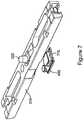
- central contact 220has inserted through a bottom opening in housing 310. Since central contact 220 is inserted through a bottom opening in housing 310, central contacting portion 221 could inadvertently be pushed all the way to the bottom of housing 310. To prevent this, embodiments of the present invention may attach a bottom stop portion 430 to a bottom of housing 310. Bottom stop portion 430 may include a raised portion 710 below contacting portion 221. This raised portion 710 may restrict the travel range of contacting portion 221. This may prevent contacting portion 221 be pushed all the way into housing 310, thereby damaging contacting structure 300. In the present invention, the center contact may have housing 310 insert molded around it and bottom stop portion 430 may not be needed.
- a piece of insulating tape 910may be wrapped around a portion of the top, sides, and bottom of housing 310.
- Insulating tape 910may include openings 912 for surface-mount contacting portions 520, 521, and 522 of the contacts in housing 310.
- Insulating tape 910may include top surface tabs 914. Top surface tabs 914 may be sandwiched between top cover 210 and housing 310, thereby helping to maintain insulating tape 910 in place.
- insulating tape 910may be Mylar tape or other type of tape or insulating layer.
- a cover 210is placed over housing 310. Again, top surface tabs 914 of insulating tape 910 may be placed between top cover 310 and housing 310, thereby holding insulating tape 910 in place.
- Top cover 210may include a raised portion 212 having openings 213 for contacts 220.
- Figure 11illustrates a completed contact structure 300 according to the present invention.
- housing 310 and cover 210may be formed of the same or different materials, such as plastic, LPS, or other non-conductive material.
- Contacting portions 221, 222, and 223,maybe formed of noncorrosive materials, such as gold, gold plated copper, gold plated nickel, gold-nickel alloy, and other materials.
- Flexible lever arms 420, 444, and 428may be formed of spring metal, sheet-metal, copper alloy, or other complaint material.
- housing 310 and cover 210may be formed using injection or other molding, printing, or other technique
- Contact portions 221, 222, and 223 and flexible lever arms 420, 424, and 428may be machined, stamped, coined, forged, printed, or formed in different ways.
- Contact portions 221, 222, and 223may be attached to flexible lever arms 420, 424, and 428 by riveting, soldering, spot-welding, or other technique, or they may be formed as a single unit.
- Housing 310 and cover 210may be formed around contacts 220 using injection molding.
- Figure 12illustrates another contact structure in a device enclosure according to an example to aid understanding of the present invention.
- a raised portion 1210 of a contact structuremay be fit in an opening in device enclosure 1200.
- Raised portion 1210may include contacts 1220 each surrounded by an individual raised portion 1212.
- Contacts 1220may be low-profile contacts. Such contacts may allow a contact structure to provide contacts for a connector without consuming a large volume in the electronic device housed by enclosure 1200.
- contacts 1220may be spring- biased contacts.
- contacts 1220may be biased by a spring, flexible arm, or other flexible structure such that they may be pushed or depressed and may return to their original position once released.
- Spring-biased contactsmay provide an amount of compliance with contacts in a corresponding connector, thereby assisting in forming electrical connections between multiple contacts 1220 and corresponding contacts of a second connector on a second device (not shown.)
- examples to aid understanding of the present inventionmay provide contact structures having low-profile, spring-biased contacts.
- An exampleis shown in the following figure.
- FIG. 13illustrates a contact structure according to an example to aid understanding of the present invention.
- This contact structuremay include housing 1320 having a number of slots for contact portions 1222.
- Contacts 1220may connect to contacting portions 1222 via flexible arms 1224.
- This contact structuremay further include a top plate or cover 1310 having a raised portion 1210.
- Raised portion 1210may include further raised portions 1212 around each opening 1213. Each opening 1213 may allow a connection to be made to contacting portion 1220.
- This contact structuremay further include a bottom plate 1330.
- Bottom plate 1330may include tabs 1350 to fit in notch 1352 in top plate or cover 1310 and notch 1354 in housing 1320 to secure top plate or cover 1310, housing 1320, and bottom plate 1330 together as a unit.
- housing 1320, cover 1310, and bottom plate 1330may be formed of the same or different materials, such as plastic, LPS, or other non-conductive material.
- Contacting portions 1220may be formed of noncorrosive materials, such as gold, gold plated copper, gold plated nickel, gold-nickel alloy, and other materials.
- Flexible lever arms 1224 and contact portions 1222may be formed of spring metal, sheet-metal, copper alloy, or other complaint material.
- housing 1320, cover 1310, and bottom plate 1330may be formed using injection or other molding, printing, or other technique
- Contacting portions 1220, flexible lever arms 1224, and contact portions 1222may be machined, stamped, coined, forged, printed, or formed in different ways.
- Contact portions 1220may be attached to flexible lever arms 1224 by riveting, soldering, spot-welding, or other technique, or they may be formed as a single unit.
- Housing 1320, cover 1310, and bottom plate 1330may be formed around contacts 1220 using injection molding.
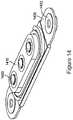
- FIG. 14illustrates a contact structure in a device enclosure according to an example to aid understanding of the present invention.
- a raised portion 1410 of a contact structuremay be fit in an opening in a device enclosure.
- Raised portion 1410may include contacts 1420.
- This contact structuremay include bracket 1430. Bracket 1430 may be fixed to a lid, device enclosure, or other structure by inserting fasteners into threaded inserts 1432.
- Contacts 1420may be low-profile contacts. Such contacts may allow a contact structure to provide contacts for a connector without consuming a great deal of volume in the electronic device housed by the enclosure.
- contacts 1420may be spring-biased contacts.
- contacts 1420may be biased by a spring, flexible arm, or other flexible structure such that they may be pushed or depressed and may return to their original position once released.
- Spring-biased contactsmay provide an amount of compliance with contacts in a corresponding connector, thereby assisting in forming electrical connections between multiple contacts 1420 and corresponding contacts of a second connector on a second device (not shown.)
- This contact structuremay be assembled in various ways. An example is shown in the following figure.
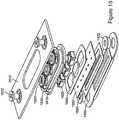
- FIG. 15is an exploded view of a contact structure according to an example to aid understanding of the present invention.
- a flexible circuit board 1550may include a number of openings for terminals of spring-biased contacts 1420.
- Spring-biased contacts 1420may be attached to flexible circuit board 1550 by inserting terminals of spring-biased contacts 1420 into the openings in flexible circuit board 1550 and soldering.
- a cap having openings for contacts 1420may be placed over contacts 1420.
- Capmay further include gaskets 1520 in openings in cap 1410.
- An additional gasket 1530may be placed or formed between contacts 1420 and inside edges of openings in cap 1410.
- Gaskets 1520 and 1530may be formed of silicone or other sealing material.
- Cap 1410may be formed as a two shot injection molded process, where the main part of cap 1410 is formed in a first shot and gaskets 1520 are formed in a second shot. Cap 1410 maybe attached to flexible circuit board 1550 using a double-sided adhesive layer 1540. Adhesive layer 1540 may be a heat activated film or adhesive layer. Bracket 1430 may be attached using a second adhesive layer 1560 to a bottom of flexible circuit board 1550. Adhesive layer 1560 may also be a heat activated film or adhesive layer. Lid 1510 may be placed over cap 1410. Lid 1510 may be a portion of a device enclosure for a device housing this contact structure. The enclosure may be conducive or nonconductive.
- Gasket 1530may be placed around a raised surface of cap 1410 and be located between cap 1410 and lid 1510. Threaded inserts 1432 may be press-fit into openings at ends of bracket 1430. Fasteners, such as screws 1512, may be inserted into openings at ends of lid 1510 and screwed into threaded inserts 1432 in bracket 1430. In other examples to aid understanding of the present invention, the threaded inserts may be replaced by threaded opening in bracket 1430.
- the contact structuremay include three contacts 1420.
- the contact structuremay include one, two, or more than three contacts 1420.
- each of the contacts 1420are located in a single raised portion, in other examples to aid understanding of the present invention, more than one raised portion may be employed, and one or more contact 1420 may be located in portions of the contact structure other than the one or more raised portions.
- the three contacts 1420are shown as being in a line, in other examples to aid understanding of the present invention, contacts 1420 may be arranged in other patterns.
- Various spring-biased contacts 1420may be used in contacting structures according to examples to aid understanding of the present invention. An example is shown in the following figures.
- Figure 16illustrates a spring-biased contact according to an example to aid understanding of the present invention.
- This spring-biased contactmay include a contacting portion 1420 supported by housing 1610.
- Terminal structure 1620may include legs that may be inserted into openings in a flexible circuit board, printed circuit board, or other appropriate substrate.
- Figure 17is an exploded view of a spring-biased contact of Figure 16 .
- housing 1610may include a central opening 1612. A first end of spring 1710 may be inserted into central opening 1612. Housing 1610 may further include notches 1616 and 1618, as well as corner notches 1614.
- a contacting portionmay have a backside cavity (not shown.)
- a second end of spring 1710may be inserted into the backside cavity of contacting portion.
- Terminal structure 1620may be fit over contacting portion such that contacting portion passes through central opening 1622 of terminal structure 1620.
- Terminal structure 1620may include legs which may fit in corner notches 1614.
- Tabs 1628 and 1626may fit in notches 1618 and 1616 in housing 1610 to secure terminal structure 1620 in place relative to housing 1610.
- Contacting portionmay include tabs 1422, which may fit under terminal structure 1620 near portion 1624 to hold contacting portion in place.
- Tabs 1628may include raised portions 1629, which may fit in the back side cavity of contacting portion. Tabs 1629 may help to ensure that electrical contact remains between contacting portion and terminal 1620 as the contacting portion is depressed towards housing 1610.
- cap 1410 and gaskets 1520may be formed of the same or different materials, such as plastic, LPS, or other non-conductive material.
- Contacting portions of spring-biased contacts 1420may be formed of noncorrosive materials, such as gold, gold plated copper, gold plated nickel, gold-nickel alloy, and other materials.
- Bracket 1430may be formed of sheet metal or other material.
- cap 1410 and gaskets 1520may be formed using injection or other molding, printing, or other technique.
- Contact portions and other conductive portions of contacts 1420may be machined, stamped, coined, forged, printed, or formed in different ways.
- Examples to aid understanding of the present inventionmay provide contact structures that may be located in various types of devices, such as portable computing devices, tablet computers, desktop computers, laptops, all-in-one computers, wearable computing devices, cell phones, smart phones, media phones, storage devices, keyboards, covers, cases, portable media players, navigation systems, monitors, power supplies, adapters, remote control devices, chargers, and other devices.
- portable computing devicestablet computers, desktop computers, laptops, all-in-one computers, wearable computing devices, cell phones, smart phones, media phones, storage devices, keyboards, covers, cases, portable media players, navigation systems, monitors, power supplies, adapters, remote control devices, chargers, and other devices.
- These devicesmay include contact structures that may provide pathways for signals and power compliant with various standards such as one of the Universal Serial Bus (USB) standards including USB Type-C, HDMI, DVI, Ethernet, DisplayPort, Thunderbolt, Lightning, JTAG, TAP, DART, DARTs, clock signals, power signals, and other types of standard, non-standard, and proprietary interfaces combinations thereof that have been developed, are being developed, or will be developed in the future.
- USBUniversal Serial Bus
- the contact structuresmay be used to convey a data signal, a power supply, and ground.
- the data signalmay be unidirectional or bidirectional and the power supply may be unidirectional or bidirectional.
Landscapes
- Engineering & Computer Science (AREA)
- Manufacturing & Machinery (AREA)
- Coupling Device And Connection With Printed Circuit (AREA)
Description
- The number of types of electronic devices that are commercially available has increased tremendously the past few years and the rate of introduction of new devices shows no signs of abating. Devices, such as tablet, laptop, netbook, desktop, and all-in-one computers, cell, smart, and media phones, storage devices, portable media players, navigation systems, monitors, and others, have become ubiquitous.
- Power and data may be provided from one device to another over cables that may include one or more wire conductors, fiber optic cables, or other conductor. Connector inserts may be located at each end of these cables and may be inserted into connector receptacles in the communicating or power transferring devices. In other systems, contacts on the devices may come into direct contact with each other without the need for intervening cables.
- In systems where contacts on two electronic devices come into direct contact with each other, it may be difficult to generate enough normal force to ensure a good electrical connection between contacts in the two devices. To provide a sufficient normal force, contacts may often have a substantial depth and consume a relatively large volume of space in the electronic device. The loss of this space may mean that the electronic device is either larger or only includes a reduced set of functionality.
- These electronic devices may be manufactured in large numbers. A corresponding number of contact structures may be manufactured for use in these devices. Any simplification in the manufacturing process of these contact structures may yield tremendous savings in the manufacturing of these electronic devices.
- Thus, what is needed are contact structures that are readily manufactured, where contacts in the contact structures provide a sufficient normal force while consuming a minimal amount of surface area, depth, and volume in an electronic device.
US 2013/183861 A1 discloses an electrical connector including a base portion received in a first insulating housing and a contacting potion extending upwardly from the base portion and received in a second insulating housing.US 2014/377992 A1 discloses an electrical connector comprising an insulating housing with a plurality of signal contacts and a plurality of grounding contacts received therein, each of the grounding contacts including a body portion, a spring arm extending upwardly from the body portion, the spring arm including a contact portion at the end thereof.US 5 213 314 A discloses a spring contact device consisting of an insulative case having at least one pair of slots extending upwardly from a bottom thereof and a contact spring 1 which includes a leaf spring portion made from a spring metal sheet; a U-shaped contact portion which projects through a top of the case. A terminal portion projects downwardly from a bottom of the case and at least one pair of lugs extend upwardly from a lower section of the U-shaped leaf spring portion and press fitted into the slots for securing the spring contact to the case.US 2009 / 241004 A1 discloses a battery connector including an insulating body and a conductive terminal disposed within a receiving space of the insulating body, a fixing portion within the receiving space, and a U-shape contacting portion with a slot defining two U-shape elastic arms which protrude from an opening of a sidewall of the insulating body.US 2013 / 035006 A1 discloses a contact terminal including a contact pin and a plate spring configured to support the contact pin, wherein a portion of the plate spring is connected to a circuit board, wherein the contact pin can be connected to a counterpart while being supported by the plate spring.JP S63 23776 U US 5 980 335 A discloses a one-piece electrical terminal which includes a strip of conductive metal material having a contact portion fabricated of a relatively soft metal drawn into a shaped contact, wherein the terminating portion is integral with the contact portion and is fabricated of a relatively hard tempered metal formed into a spring arm supporting the contact.US 7 575 469 B1 discloses a battery connector including a housing having terminal chambers to receive plural terminals having elastic and contact portions extending therefrom and projecting out of the terminal chambers for electrically contacting a battery, wherein the housing defines a positioning recess across fronts of the terminal chambers.WO 2005/013430 A1 discloses a connector for electrically connecting two electrical points and having one or more connector terminals arranged in a connector housing and comprising a resilient arm portion which bends or deflects about a first pivot portion when the connector terminal is compressed initially or about a second pivot point when further compressed subsequently. The present invention is defined by the features of the independent claims. Preferred advantageous embodiments thereof are defined by the features of the dependent claims.- Accordingly, embodiments of the present invention may provide contact structures that are readily manufactured, where contacts in the contact structures provide a sufficient normal force while consuming a minimal amount of surface area, depth, and volume in an electronic device. The problem is solved by the contact structure disclosed in claim 1 and the method of assembling such a contact structure as defined in claim 5.
- An illustrative embodiment of the present invention may provide contact structures that may provide movable contacts at a surface of an electronic device. The contact structures may include a nonconductive housing supporting one, two, three, or more conductive contacts. According to the invention, each contact is located at an end of a flexible lever arm, where a remote end of the arm may be fixed to the housing. The contacts may have contacting portions that emerge from corresponding openings in the housing.
- These contact structures may be manufactured in various ways. For example, the contacting portions may be attached to ends of the flexible lever arms by riveting, soldering, or the contacting portions and the flexible lever arms may be formed as a single piece. The contacting portions may be formed of the same or different materials. For example, the contacting portions may be formed of a material that provides a low resistance and low corrosion, while the flexible lever arms may be formed of a material chosen for its flexibility and its ability to withstand fatigue and cold-working. The contacting portion may have a narrowed tail extending from a wider body, where the narrowed tail may be inserted into an opening at an end of the flexible lever arm. The narrowed tail may extend through and beyond the flexible lever arm. Force may be applied to the narrowed tail causing it to expand outward, for example in a riveting process. The contacting portion may be held in place in the opening on the flexible lever arm on one side by the expanded narrowed tail and on the other side by the wider body. Each flexible lever arm may have a surface-mount contacting portion at an end remote from the contacting portion. Each flexible lever arm may further include a barb to be inserted into a notch or groove in the contact structure housing. In the present invention the center contact has the housing insert molded around it such that it does not require a barb. The contacts may be arranged in a line in the housing, though they may be arranged in other patterns. Contacts that are centrally located in the housing may be inserted into the housing from a bottom side and fixed in place by inserting their barbs into slots or grooves in the housing. Again, in other embodiments of the present invention these center contacts may have the housing insert molded around it. In examples, not forming part of the invention, structures may be placed under the contacting portions of the central contacts to limit their travel such that they cannot be pushed all the way into the housing, though these may not be useful when the housing is insert molded around the center contact. Contacts located at the ends may be slid into the housing using slots in the housing. The side contacts may also be fixed in place by inserting their barbs into slots or grooves in the housing. Insulating tape may be used to electrically insulate the housing. A cover having openings for the contacting portions may be fit over the housing. The cover may have a raised portion around the openings for the contacts to fit in an opening of a device enclosure of the electronic device housing the contact structure.
- Another illustrative embodiment of the present invention may provide contact structures that may provide movable contacts at a surface of an electronic device. The contact structures may include a nonconductive housing having slots for a number of conductive contacts. Each contact may include a contacting portion attached to a flexible lever arm. The flexible lever arm may attach to a contact length that may be located in a slot in the housing. A cover may fit over the housing. The cover may include a raised portion having a number of openings, each opening for a corresponding contacting portion of a contact. The openings may be located in raised portion. The raised portion may fit in an opening of a device enclosure of the electronic device housing the contact structure. The contact structure may further include a bottom plate. The bottom plate may include side tabs that fit in notches or slots in sides of the housing and cover to fix the cover and housing in place relative to the bottom plate.
- Another illustrative embodiment of the present invention may provide contact structures that may provide movable contacts at a surface of an electronic device. This contact structure may include a nonconductive housing supporting one, two, three, or more conductive contacts. Each contact may be a spring-biased contact. The spring-biased contacts may have contacting portions that emerge from corresponding openings in the housing.
- These contact structures may be manufactured in various ways. For example, the spring-biased contacts may be attached to a flexible circuit board. Terminal contacts on the spring-biased contacts may be soldered into opening in the flexible circuit board. A layer of double-sided adhesive may be used to fix the flexible circuit board to a bracket. Threaded inserts may be placed in one or more openings in the bracket, or the ends of the brackets may include threaded openings. For example, the threaded inserts may be press-fit into openings near ends of the bracket. A cap may be formed where the cap may include openings for contacting portions of the spring-biased contacts. The openings may be located on a raised portion that may be arranged to fit in an opening of a device enclosure of the electronic device housing the contact structure. The cap may include gaskets that form rings around the contacting portions of the spring-biased contacts between the contacting portions and inside edges of the openings in the raised portion of the cap. The cap may be formed as a double-shot injection molded part where the gaskets are the second injection-molded shot. The cap may be fixed to the flexible circuit board using a double-sided adhesive layer. A lid, which may be part of a device enclosure for the device housing the contact structure, may be fixed over the top of the contact structure by screws or other fasteners that may be fit into openings in the lid and inserted into the threaded inserts. The raised portion of the cap may fit into a central opening in the lid. A gasket may be placed around the raised portion of the cap and between the cap and the lid to prevent the ingress of liquid, moisture, debris, or other substances into the electronic device housing the contact structure.
- The spring-biased contacts may be formed in various ways. For example, a housing have a central hole may be provided. A spring may be fit into the central hole. A contacting portion having a backside opening may be fit over the spring such that one end of the spring is in the central hole of the housing and the other end of the spring is in the backside opening of the contacting portion. A terminal structure may be fit over the contacting portion and top of the housing. A tab on the contacting portion may be under the terminal structure such that the contacting portion is held in place. Tabs on the terminal structure may fit in notches or slots in the housing to secure the terminal structure in place relative to the housing. The terminal structure may include through-hole portions that may be inserted and soldered in place in openings in the flexible circuit board.
- Embodiments of the present invention may provide contact structures that may be located in various types of devices, such as portable computing devices, tablet computers, desktop computers, laptops, all-in-one computers, wearable computing devices, cell phones, smart phones, media phones, storage devices, keyboards, covers, cases, portable media players, navigation systems, monitors, power supplies, adapters, remote control devices, chargers, and other devices. These contact structures may provide pathways for signals and power compliant with various standards such as one of the Universal Serial Bus (USB) standards including USB Type-C, High-Definition Multimedia Interface® (HDMI), Digital Visual Interface (DVI), Ethernet, DisplayPort, Thunderbolt™, Lightning™, Joint Test Action Group (JTAG), test-access-port (TAP), Directed Automated Random Testing (DART), universal asynchronous receiver/transmitters (UARTs), clock signals, power signals, and other types of standard, non-standard, and proprietary interfaces and combinations thereof that have been developed, are being developed, or will be developed in the future. In one example, the contact structures may be used to convey a data signal, a power supply, and ground. In various embodiments of the present invention, the data signal may be unidirectional or bidirectional and the power supply may be unidirectional or bidirectional.
- Various embodiments of the present invention may incorporate one or more of these and the other features described herein. A better understanding of the nature and advantages of the present invention may be gained by reference to the following detailed description and the accompanying drawings.
Figure 1 illustrates an electronic system according to an embodiment of the present invention;Figure 2 illustrates a contact structure in a device enclosure according to an embodiment of the present invention;Figure 3 illustrates a portion of an electronic device according to an embodiment of the present invention;Figure 4 illustrates a side view of a contact structure according to an embodiment of the present invention;Figures 5 ,6 ,8-11 illustrate a method of assembling a contact structure according to an embodiment of the present invention;Figure 7 illustrates an example of a method of assembling a contact structure that does not from part of the invention;Figure 12 illustrates another contact structure in a device enclosure according to an example to aid understanding of the present invention;Figure 13 illustrates a contact structure according to an example to aid understanding of the present invention;Figure 14 illustrates a contact structure in a device enclosure according to an example to aid understanding of the present invention;Figure 15 is an exploded view of a contact structure according to an example to aid understanding of the present invention;Figure 16 illustrates a spring-biased contact according to an example to aid understanding of the present invention; andFigure 17 is an exploded view of a spring-biased contact ofFigure 16 .Figure 1 illustrates an electronic system according to an embodiment of the present invention. This figure, as with the other included figures, is shown for illustrative purposes and does not limit either the possible embodiments of the present invention or the claims.- In this example,
host device 110 may be connected toaccessory device 120 in order to share data, power, or both. Specifically,contacts 112 onhost device 110 may be electrically connected tocontacts 220 onaccessory device 120.Contacts 112 onhost device 110 may be electrically connected tocontacts 220 onaccessory device 120 viacable 130. In other embodiments of the present invention,contacts 112 onhost device 110 may be directly and electrically connected tocontacts 220 onaccessory device 120. - To facilitate a direction connection between
contacts 112 onhost device 110 andcontacts 220 onaccessory device 120,contacts 220 may be part of a surface-mount contact structure. An example of a surface-mount contact structure that may includecontacts 220 is shown in the following figures. Figure 2 illustrates a contact structure in a device enclosure according to an embodiment of the present invention. In this example, a raisedportion 212 of a contact structure may be placed in an opening indevice enclosure 230. The raisedportion 212 of the contact structure may include openings for a number ofcontacts 220.Contacts 220 may be low-profile contacts. Such contacts may allow a contact structure to provide contacts for a connector without consuming a large volume in the electronic device housed byenclosure 230. In various embodiments the present invention,contacts 220 may be spring-biased contacts. For example,contacts 220 may be biased by a spring, flexible arm, or other flexible structure such that they may be pushed or depressed and may return to their original position once released. Spring-biased contacts may provide an amount of compliance with contacts in a corresponding connector, thereby assisting in forming electrical connections betweenmultiple contacts 220 and corresponding contacts of a second connector on a second device (not shown.)- Accordingly, embodiments of the present invention may provide contact structures having low-profile, spring-biased contacts. An example is shown in the following figure.
Figure 3 illustrates a portion of an electronic device according to an embodiment of the present invention. This figure illustrates acontact structure 300 having a raisedportion 212 on acover 210 that is fit on a top side ofhousing 310. Raisedportion 212 may be arranged to fit anopening 232 indevice enclosure 230.Contact structure 300 and may support a number ofcontacts 220 each in openings in raisedportion 212.Contacts 220 may emerge from bottom ofhousing 300 and be connected to interconnect 320.- In this example,
contact structure 300 may include threecontacts 220. Also, while in this example each of thecontacts 220 are located in a single raisedportion 212, in other embodiments of the present invention, more than one raisedportion 212 may be employed, and one ormore contact 220 may be located in portions ofcontact structure 300 other than the one or more raisedportions 212. Also, while the threecontacts 220 are shown as being in a line, in other embodiments of the present invention,contacts 220 may be arranged in other patterns. Figure 4 illustrates a side view of a contact structure according to the present invention.Contact structure 300 is located in an electronicdevice having housing 230. As before, raisedportion 212 ofcover 210 ofcontact structure 300 may be located in an opening indevice enclosure 230.Housing 310 ofcontact structure 300 supports contacts having contactingportions portions flexible lever arms housing 310. Specifically,flexible lever arm 420 includesbarb 421 andflexible lever arm 428 includesbarb 429. In the present invention, the center contact hashousing 310 insert molded around it.- In an example, not forming part of the invention, during assembly, the central contact including
contact portion 222 may be inserted through an opening in a bottom ofhousing 210. Without more, contactingportion 222 could be pushed deep intohousing 310. In some instances, contactingstructure 222 could be pushed belowcover 210. If contactingportion 222 were to be laterally offset at this time, contactingportion 222 may not emerge from its opening incover 210. Accordingly, abottom stop portion 430 may be located under contactingportion 222.Bottom stop portion 430 may limit a depth to which contactingportion 222 may be depressed, thereby preventing possible damage to contactstructure 300. In the present invention, the center contact hashousing 310 insert molded around it such thatbottom stop portion 430 is be needed. Contacts structure 300 may be formed in various ways. An example is shown in the following figure.Figures 5-11 illustrate a method of assembling a contact structure according to an embodiment of the present invention. InFigure 5 , contacts for a contact structure according to an embodiment of the present invention, such ascontact structure 300, may be formed. These contacts include contactingportions portions flexible lever arms Flexible lever arm 420 may terminate in afirst barb 421 and include a surface-mount contact portion 520.Flexible lever arm 424 may terminate in surface-mount contacting portion 521.Flexible lever arm 428 includesbarb 429 and may terminate in surface-mount contacting portion 522. In the present invention, the center contact hashousing 310 insert molded around it.- Contacting
portions flexible lever arms portion 221 may include a narrowedtail portion 228 belowledge 227.Narrowed end portion 228 may be inserted intoopening 226 inflexible lever arm 420.Ledge 227 may rest on a top surface offlexible lever arm 420 aroundopening 226.Narrowed end 228 may have a force applied such that it widens, for example, by riveting. In this way, contactingportion 221 may be secured toflexible arm 420 byledge 227 and the widened portion of narrowedtail 228. When contactingstructure 300 is mounted on a board or other appropriate substrate, surface-mount contacting portions portions - In
Figure 6 , at least some of contactingportion 221 may emerge from a top surface ofhousing 310. In the present invention,housing 310 is insert molded around the central contact. - In
Figure 7 , that illustrates an example that does not form part of the invention,central contact 220 has inserted through a bottom opening inhousing 310. Sincecentral contact 220 is inserted through a bottom opening inhousing 310, central contactingportion 221 could inadvertently be pushed all the way to the bottom ofhousing 310. To prevent this, embodiments of the present invention may attach abottom stop portion 430 to a bottom ofhousing 310.Bottom stop portion 430 may include a raisedportion 710 below contactingportion 221. This raisedportion 710 may restrict the travel range of contactingportion 221. This may prevent contactingportion 221 be pushed all the way intohousing 310, thereby damaging contactingstructure 300. In the present invention, the center contact may havehousing 310 insert molded around it andbottom stop portion 430 may not be needed. - In
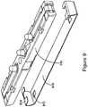
Figure 8 , side contacts including contactingportions housing 310 usingslots Flexible lever arm 420 is pushed intohousing 310 untilbarb 421 is inserted into a groove or notch inhousing 310. Similarly,flexible lever arm 428 is pushed intohousing 310 untilbarb 429 is inserted into a groove or notch inhousing 310. - In
Figure 9 , a piece of insulatingtape 910 may be wrapped around a portion of the top, sides, and bottom ofhousing 310. Insulatingtape 910 may includeopenings 912 for surface-mount contacting portions housing 310. Insulatingtape 910 may includetop surface tabs 914.Top surface tabs 914 may be sandwiched betweentop cover 210 andhousing 310, thereby helping to maintaininsulating tape 910 in place. In various embodiments of the present invention, insulatingtape 910 may be Mylar tape or other type of tape or insulating layer. - In
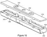
Figure 10 , acover 210 is placed overhousing 310. Again,top surface tabs 914 ofinsulating tape 910 may be placed betweentop cover 310 andhousing 310, thereby holdinginsulating tape 910 in place.Top cover 210 may include a raisedportion 212 havingopenings 213 forcontacts 220. Figure 11 illustrates a completedcontact structure 300 according to the present invention.- In various embodiments of the present invention, different portions of
contact structure 300 and other contact structures may be formed of various materials. For example,housing 310 and cover 210 may be formed of the same or different materials, such as plastic, LPS, or other non-conductive material. Contactingportions Flexible lever arms - In various embodiments of the present invention, different portions of
contact structure 300 and other contact structures may be formed in various ways. For example,housing 310 and cover 210 maybe formed using injection or other molding, printing, or othertechnique Contact portions flexible lever arms portions flexible lever arms Housing 310 and cover 210 may be formed aroundcontacts 220 using injection molding. Figure 12 illustrates another contact structure in a device enclosure according to an example to aid understanding of the present invention. In this example, a raisedportion 1210 of a contact structure may be fit in an opening indevice enclosure 1200. Raisedportion 1210 may includecontacts 1220 each surrounded by an individual raisedportion 1212.Contacts 1220 may be low-profile contacts. Such contacts may allow a contact structure to provide contacts for a connector without consuming a large volume in the electronic device housed byenclosure 1200. In various examples to aid understanding of the present invention,contacts 1220 may be spring- biased contacts. For example,contacts 1220 may be biased by a spring, flexible arm, or other flexible structure such that they may be pushed or depressed and may return to their original position once released. Spring-biased contacts may provide an amount of compliance with contacts in a corresponding connector, thereby assisting in forming electrical connections betweenmultiple contacts 1220 and corresponding contacts of a second connector on a second device (not shown.)- Accordingly, examples to aid understanding of the present invention may provide contact structures having low-profile, spring-biased contacts. An example is shown in the following figure.
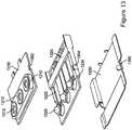
Figure 13 illustrates a contact structure according to an example to aid understanding of the present invention. This contact structure may includehousing 1320 having a number of slots forcontact portions 1222.Contacts 1220 may connect to contactingportions 1222 viaflexible arms 1224.- This contact structure may further include a top plate or
cover 1310 having a raisedportion 1210. Raisedportion 1210 may include further raisedportions 1212 around eachopening 1213. Eachopening 1213 may allow a connection to be made to contactingportion 1220. - This contact structure may further include a
bottom plate 1330.Bottom plate 1330 may includetabs 1350 to fit innotch 1352 in top plate orcover 1310 andnotch 1354 inhousing 1320 to secure top plate orcover 1310,housing 1320, andbottom plate 1330 together as a unit. - In various examples to aid understanding of the present invention, different portions of this contact structure and other contact structures may be formed of various materials. For example,
housing 1320,cover 1310, andbottom plate 1330 may be formed of the same or different materials, such as plastic, LPS, or other non-conductive material. Contactingportions 1220 may be formed of noncorrosive materials, such as gold, gold plated copper, gold plated nickel, gold-nickel alloy, and other materials.Flexible lever arms 1224 andcontact portions 1222 may be formed of spring metal, sheet-metal, copper alloy, or other complaint material. - In various examples to aid understanding of the present invention, different portions of this contact structure and other contact structures may be formed in various ways. For example,
housing 1320,cover 1310, andbottom plate 1330 may be formed using injection or other molding, printing, or othertechnique Contacting portions 1220,flexible lever arms 1224, andcontact portions 1222 may be machined, stamped, coined, forged, printed, or formed in different ways.Contact portions 1220 may be attached toflexible lever arms 1224 by riveting, soldering, spot-welding, or other technique, or they may be formed as a single unit.Housing 1320,cover 1310, andbottom plate 1330 may be formed aroundcontacts 1220 using injection molding. Figure 14 illustrates a contact structure in a device enclosure according to an example to aid understanding of the present invention. In this example, a raisedportion 1410 of a contact structure may be fit in an opening in a device enclosure. Raisedportion 1410 may includecontacts 1420. This contact structure may includebracket 1430.Bracket 1430 may be fixed to a lid, device enclosure, or other structure by inserting fasteners into threadedinserts 1432.Contacts 1420 may be low-profile contacts. Such contacts may allow a contact structure to provide contacts for a connector without consuming a great deal of volume in the electronic device housed by the enclosure. In various examples to aid understanding the present invention,contacts 1420 may be spring-biased contacts. For example,contacts 1420 may be biased by a spring, flexible arm, or other flexible structure such that they may be pushed or depressed and may return to their original position once released. Spring-biased contacts may provide an amount of compliance with contacts in a corresponding connector, thereby assisting in forming electrical connections betweenmultiple contacts 1420 and corresponding contacts of a second connector on a second device (not shown.)- This contact structure may be assembled in various ways. An example is shown in the following figure.
Figure 15 is an exploded view of a contact structure according to an example to aid understanding of the present invention. In this example, aflexible circuit board 1550 may include a number of openings for terminals of spring-biasedcontacts 1420. Spring-biasedcontacts 1420 may be attached toflexible circuit board 1550 by inserting terminals of spring-biasedcontacts 1420 into the openings inflexible circuit board 1550 and soldering. A cap having openings forcontacts 1420 may be placed overcontacts 1420. Cap may further includegaskets 1520 in openings incap 1410. Anadditional gasket 1530 may be placed or formed betweencontacts 1420 and inside edges of openings incap 1410.Gaskets Cap 1410 may be formed as a two shot injection molded process, where the main part ofcap 1410 is formed in a first shot andgaskets 1520 are formed in a second shot.Cap 1410 maybe attached toflexible circuit board 1550 using a double-sided adhesive layer 1540.Adhesive layer 1540 may be a heat activated film or adhesive layer.Bracket 1430 may be attached using asecond adhesive layer 1560 to a bottom offlexible circuit board 1550.Adhesive layer 1560 may also be a heat activated film or adhesive layer.Lid 1510 may be placed overcap 1410.Lid 1510 may be a portion of a device enclosure for a device housing this contact structure. The enclosure may be conducive or nonconductive.Gasket 1530 may be placed around a raised surface ofcap 1410 and be located betweencap 1410 andlid 1510. Threadedinserts 1432 may be press-fit into openings at ends ofbracket 1430. Fasteners, such asscrews 1512, may be inserted into openings at ends oflid 1510 and screwed into threadedinserts 1432 inbracket 1430. In other examples to aid understanding of the present invention, the threaded inserts may be replaced by threaded opening inbracket 1430.- In this example, the contact structure may include three
contacts 1420. In other examples to aid understanding of the present invention, the contact structure may include one, two, or more than threecontacts 1420. Also, while in this example each of thecontacts 1420 are located in a single raised portion, in other examples to aid understanding of the present invention, more than one raised portion may be employed, and one ormore contact 1420 may be located in portions of the contact structure other than the one or more raised portions. Also, while the threecontacts 1420 are shown as being in a line, in other examples to aid understanding of the present invention,contacts 1420 may be arranged in other patterns. - Various spring-biased
contacts 1420 may be used in contacting structures according to examples to aid understanding of the present invention. An example is shown in the following figures. Figure 16 illustrates a spring-biased contact according to an example to aid understanding of the present invention. This spring-biased contact may include a contactingportion 1420 supported byhousing 1610.Terminal structure 1620 may include legs that may be inserted into openings in a flexible circuit board, printed circuit board, or other appropriate substrate.Figure 17 is an exploded view of a spring-biased contact ofFigure 16 . In this example,housing 1610 may include acentral opening 1612. A first end ofspring 1710 may be inserted intocentral opening 1612.Housing 1610 may further includenotches corner notches 1614.- A contacting portion may have a backside cavity (not shown.) A second end of
spring 1710 may be inserted into the backside cavity of contacting portion. Terminal structure 1620 may be fit over contacting portion such that contacting portion passes throughcentral opening 1622 ofterminal structure 1620.Terminal structure 1620 may include legs which may fit incorner notches 1614.Tabs notches housing 1610 to secureterminal structure 1620 in place relative tohousing 1610. Contacting portion may includetabs 1422, which may fit underterminal structure 1620 nearportion 1624 to hold contacting portion in place.Tabs 1628 may include raisedportions 1629, which may fit in the back side cavity of contacting portion.Tabs 1629 may help to ensure that electrical contact remains between contacting portion and terminal 1620 as the contacting portion is depressed towardshousing 1610.- In various examples to aid understanding of the present invention, different portions of this contact structure and other contact structures may be formed of various materials. For example,
cap 1410 andgaskets 1520 may be formed of the same or different materials, such as plastic, LPS, or other non-conductive material. Contacting portions of spring-biasedcontacts 1420 may be formed of noncorrosive materials, such as gold, gold plated copper, gold plated nickel, gold-nickel alloy, and other materials.Bracket 1430 may be formed of sheet metal or other material. - In various examples to aid understanding of the present invention, different portions of this contact structure and other contact structures may be formed in various ways. For example,
cap 1410 andgaskets 1520 may be formed using injection or other molding, printing, or other technique. Contact portions and other conductive portions ofcontacts 1420 may be machined, stamped, coined, forged, printed, or formed in different ways. - Examples to aid understanding of the present invention may provide contact structures that may be located in various types of devices, such as portable computing devices, tablet computers, desktop computers, laptops, all-in-one computers, wearable computing devices, cell phones, smart phones, media phones, storage devices, keyboards, covers, cases, portable media players, navigation systems, monitors, power supplies, adapters, remote control devices, chargers, and other devices. These devices may include contact structures that may provide pathways for signals and power compliant with various standards such as one of the Universal Serial Bus (USB) standards including USB Type-C, HDMI, DVI, Ethernet, DisplayPort, Thunderbolt, Lightning, JTAG, TAP, DART, DARTs, clock signals, power signals, and other types of standard, non-standard, and proprietary interfaces combinations thereof that have been developed, are being developed, or will be developed in the future. In one example, the contact structures may be used to convey a data signal, a power supply, and ground. In various embodiments of the present invention, the data signal may be unidirectional or bidirectional and the power supply may be unidirectional or bidirectional.
- The above description of embodiments of the invention has been presented for the purposes of illustration and description. It is not intended to be exhaustive or to limit the invention to the precise form described, and many modifications and variations are possible within the scope of the appended claims. The embodiments were chosen and described in order to best explain the principles of the invention and its practical applications to thereby enable others skilled in the art to best utilize the invention in various embodiments and with various modifications as are suited to the particular use contemplated. Thus, it will be appreciated that the invention is intended to cover all modifications and equivalents within the scope of the appended claims.
Claims (6)
- A contact structure (300) comprising:a housing (310);a first side contact (220) and a second side contact (220), each comprising:a flexible lever arm (420, 428);a contacting portion (221, 223) attached to a first end of the flexible lever arm (420, 428); anda barb (421, 429) on the flexible lever arm (420, 428), located at or near a second end of the flexible lever arm (420, 428), and inserted into the housing (310);a third central contact (220) comprising:a flexible lever arm (425);a contacting portion (222) attached to a first end of the flexible lever arm (424), wherein the housing (310) is insert molded around a portion of the third central contact (220); anda cover (210) attached to a top of the housing (310), the cover (210) comprising a raised portion (212) around a plurality of openings (213) each for a contacting portion (221, 222, 223) of the first side contact, second side contact (220) and third central contact (220),characterised in that the housing (310) comprises side slots (810, 812) on opposing sides to accept insertion of the first side contact and the second side contact (220) during assembly.
- The contact structure (300) of claim 1 wherein the contacting portion (221, 222, 223) of each contact (220) includes a widened body portion and a narrowed tail.
- The contact structure (300) of claim 2 wherein the contacting portion (221, 222, 223) of each contact (220) is riveted to the first end of the flexible lever arm (420, 424, 428).
- The contact structure of claim 1 further comprising a surface-mount contact portion (520, 521, 522) at a second end of the flexible lever arm (420, 424, 428) of each of the first side contact (220), second side contact (220), and third central contact (220).
- A method of assembling a contact structure (300), the method comprising:forming a plurality of contacts (220) by, for each contact (220):attaching a contacting portion (221, 222, 223) to a first end of a flexible lever arm (420, 424, 428);insert molding a housing (310) around a portion of fixing a central contact (220);inserting side contacts (220) in side slots (810, 812) in the housing (312) on opposing sides such that at least a portion of the contacting portion (221, 223) of each side contact (220) is exposed above the housing (310); andfixing the side contacts (220) in place in the housing (310) by inserting a barb (421, 429) of each side contact (220) in the housing (310), each barb (421, 429) on the flexible lever arm (420, 428) of a corresponding side contact (220) and located at or near a second end of the flexible lever arm (420, 428);attaching a cover (210) to the top of the housing (310), the cover (210) having a raised portion (212), the raised portion (212) having a plurality of openings (213), each opening (213) for a corresponding one of the plurality of contacts (220).
- The method of claim 5 wherein attaching a contacting portion (221, 222, 223) to a first end of a flexible lever arm comprises:inserting a narrowed tail of a contacting portion (221, 222, 223) into an opening at a first end of a flexible lever arm (420, 424, 428); andriveting the contacting portion (221, 222, 223) to the flexible lever arm (420, 424, 428).
Priority Applications (1)
| Application Number | Priority Date | Filing Date | Title |
|---|---|---|---|
| EP20162122.4AEP3723209A1 (en) | 2015-09-08 | 2016-08-31 | Electrical contact structure |
Applications Claiming Priority (2)
| Application Number | Priority Date | Filing Date | Title |
|---|---|---|---|
| US201562215592P | 2015-09-08 | 2015-09-08 | |
| US15/138,224US9893452B2 (en) | 2015-09-08 | 2016-04-26 | Low-profile spring-loaded contacts |
Related Child Applications (1)
| Application Number | Title | Priority Date | Filing Date |
|---|---|---|---|
| EP20162122.4ADivisionEP3723209A1 (en) | 2015-09-08 | 2016-08-31 | Electrical contact structure |
Publications (2)
| Publication Number | Publication Date |
|---|---|
| EP3142193A1 EP3142193A1 (en) | 2017-03-15 |
| EP3142193B1true EP3142193B1 (en) | 2020-03-11 |
Family
ID=56855295
Family Applications (2)
| Application Number | Title | Priority Date | Filing Date |
|---|---|---|---|
| EP16186530.8AActiveEP3142193B1 (en) | 2015-09-08 | 2016-08-31 | Contact structure and method of assembling thereof |
| EP20162122.4APendingEP3723209A1 (en) | 2015-09-08 | 2016-08-31 | Electrical contact structure |
Family Applications After (1)
| Application Number | Title | Priority Date | Filing Date |
|---|---|---|---|
| EP20162122.4APendingEP3723209A1 (en) | 2015-09-08 | 2016-08-31 | Electrical contact structure |
Country Status (7)
| Country | Link |
|---|---|
| US (2) | US9893452B2 (en) |
| EP (2) | EP3142193B1 (en) |
| JP (1) | JP6572186B2 (en) |
| KR (3) | KR101868929B1 (en) |
| CN (3) | CN205985467U (en) |
| AU (1) | AU2016222504B2 (en) |
| TW (1) | TWI631774B (en) |
Families Citing this family (13)
| Publication number | Priority date | Publication date | Assignee | Title |
|---|---|---|---|---|
| US10579097B2 (en) | 2015-09-04 | 2020-03-03 | Apple Inc. | Electronic device with contacts flush with housing |
| US9778705B2 (en) | 2015-09-04 | 2017-10-03 | Apple Inc. | Electronic device with moveable contacts at an exterior surface |
| US10224661B2 (en)* | 2015-09-08 | 2019-03-05 | Apple Inc. | Low-profile spring-loaded contacts |
| US9948018B2 (en) | 2015-09-08 | 2018-04-17 | Apple Inc. | Low-profile power and data contacts |
| US9941627B2 (en) | 2015-09-30 | 2018-04-10 | Apple Inc. | Magnetic surface contacts |
| US10707627B2 (en) | 2017-09-29 | 2020-07-07 | Apple Inc. | Hybrid connector |
| USD971853S1 (en)* | 2021-03-23 | 2022-12-06 | Hearthero, Inc. | Cardiac pad wire connector |
| US11862894B1 (en)* | 2021-09-16 | 2024-01-02 | Lunar Energy, Inc. | Electromechanical connector |
| TWI844382B (en)* | 2023-06-02 | 2024-06-01 | 啟碁科技股份有限公司 | Electronic device |
| US12299218B2 (en) | 2023-06-11 | 2025-05-13 | Remarkable As | Active pen-stylus precise eraser |
| USD1092467S1 (en) | 2023-11-13 | 2025-09-09 | Remarkable As | Tablet computer |
| US12411561B1 (en) | 2024-07-08 | 2025-09-09 | Remarkable As | Marker protection system |
| US12416999B1 (en) | 2024-07-08 | 2025-09-16 | Remarkable As | Replaceable conductive marker tip |
Citations (2)
| Publication number | Priority date | Publication date | Assignee | Title |
|---|---|---|---|---|
| WO2005013430A1 (en)* | 2003-08-01 | 2005-02-10 | Fci Asia Technology Pte Ltd | Connector |
| US7575469B1 (en)* | 2008-09-05 | 2009-08-18 | Cheng Uei Precision Industry Co., Ltd. | Battery connector |
Family Cites Families (44)
| Publication number | Priority date | Publication date | Assignee | Title |
|---|---|---|---|---|
| GB8612745D0 (en) | 1986-05-27 | 1986-07-02 | Russel Finex | Vibratory sieving apparatus |
| JPH0311823Y2 (en) | 1986-07-30 | 1991-03-20 | ||
| CN2059846U (en)* | 1989-07-17 | 1990-08-01 | 陶根鱼 | Medical treatment apparatus for hemiplegia |
| JPH083932Y2 (en) | 1990-09-13 | 1996-01-31 | ヒロセ電機株式会社 | Spring contacts |
| JPH0577772A (en) | 1991-09-20 | 1993-03-30 | Tokico Ltd | Wall surface traveling device |
| JP2597826Y2 (en) | 1992-03-19 | 1999-07-19 | 有限会社ヨシ・コーポレーション | Spring connection terminal |
| JPH0662474A (en) | 1992-04-22 | 1994-03-04 | Gold Star Co Ltd | Remote-controlled system |
| US5295844A (en)* | 1992-08-25 | 1994-03-22 | Mitsumi Electric Co., Ltd. | Connector |
| JPH0662474U (en) | 1993-02-10 | 1994-09-02 | 株式会社ヨコオ | Connector for electrical connection |
| JP3406383B2 (en) | 1994-06-20 | 2003-05-12 | 石川島建材工業株式会社 | Subgrade ground covering construction method |
| US5980335A (en)* | 1998-03-27 | 1999-11-09 | Molex Incorporated | Electrical terminal |
| US20040209489A1 (en) | 2003-04-21 | 2004-10-21 | Clapper Edward O. | Apparatus for automatic docking |
| KR100568177B1 (en) | 2003-06-23 | 2006-04-05 | 삼성전자주식회사 | Connector and Notebook Computer Using the Same |
| DE202004005273U1 (en)* | 2004-04-02 | 2004-06-03 | Rosenberger Hochfrequenztechnik Gmbh & Co | Coaxial connector for printed circuit boards with spring-loaded tolerance compensation |
| JP4153549B1 (en) | 2007-06-28 | 2008-09-24 | タイコエレクトロニクスアンプ株式会社 | Waterproof connector, waterproof connector mounting structure, and waterproof connector mounting method |
| US7510444B2 (en)* | 2007-07-17 | 2009-03-31 | Cheng Uei Precision Industry Co., Ltd. | SIM card connector |
| TWM324906U (en)* | 2007-07-20 | 2008-01-01 | Advanced Connectek Inc | Electrical connector |
| TWM344641U (en) | 2008-04-01 | 2008-11-11 | Htc Corp | Battery connector |
| US7933123B2 (en) | 2008-04-11 | 2011-04-26 | Apple Inc. | Portable electronic device with two-piece housing |
| US7661968B1 (en)* | 2008-11-24 | 2010-02-16 | Cheng Uei Precision Industry Co., Ltd. | Electrical connector |
| US8310457B2 (en) | 2009-06-30 | 2012-11-13 | Research In Motion Limited | Portable electronic device including tactile touch-sensitive input device and method of protecting same |
| US8385060B2 (en) | 2009-08-31 | 2013-02-26 | Apple Inc. | Handheld computing device |
| US8344836B2 (en) | 2010-09-17 | 2013-01-01 | Apple Inc. | Protective cover for a tablet computer |
| US8427825B2 (en) | 2010-10-19 | 2013-04-23 | Research In Motion Limited | External electrical connection for a portable electronic device |
| US9335793B2 (en) | 2011-01-31 | 2016-05-10 | Apple Inc. | Cover attachment with flexible display |
| ITMI20110127U1 (en) | 2011-04-14 | 2012-10-15 | Tucano S R L | HOUSING FOR A TABLET ELECTRONIC DEVICE, IN PARTICULAR A COMPUTER TABLET |
| KR101817804B1 (en) | 2011-08-03 | 2018-01-11 | 삼성전자주식회사 | Contact terminal |
| TWI495200B (en) | 2012-01-13 | 2015-08-01 | Hon Hai Prec Ind Co Ltd | Electrical connector |
| US9460029B2 (en) | 2012-03-02 | 2016-10-04 | Microsoft Technology Licensing, Llc | Pressure sensitive keys |
| US9075566B2 (en) | 2012-03-02 | 2015-07-07 | Microsoft Technoogy Licensing, LLC | Flexible hinge spine |
| US8873227B2 (en) | 2012-03-02 | 2014-10-28 | Microsoft Corporation | Flexible hinge support layer |
| JP5896786B2 (en) | 2012-03-02 | 2016-03-30 | 株式会社ヨコオ | Electrical connector |
| US9209547B2 (en)* | 2012-06-08 | 2015-12-08 | Apple Inc. | Connector adapter |
| WO2014021847A1 (en) | 2012-07-31 | 2014-02-06 | Hewlett-Packard Development Company, L.P. | Magnetic connector for a computing device |
| US9326576B2 (en) | 2012-08-08 | 2016-05-03 | Apple Inc. | Cover for an electronic device |
| US9148474B2 (en) | 2012-10-16 | 2015-09-29 | Hand Held Products, Inc. | Replaceable connector |
| US9559456B2 (en) | 2013-03-15 | 2017-01-31 | Google Technology Holdings LLC | Magnetic electrical connection system for an electronic device |
| TWM468799U (en) | 2013-06-19 | 2013-12-21 | Hon Hai Prec Ind Co Ltd | Electrical connector |
| US9149100B2 (en) | 2013-08-07 | 2015-10-06 | ACCO Brands Corporation | Case for a portable electronic device |
| US9485338B2 (en) | 2013-09-04 | 2016-11-01 | Apple Inc. | Features and manufacturing methods for a case for a portable electronic device |
| US8817457B1 (en) | 2014-01-02 | 2014-08-26 | ZAGG Intellectual Property Holding Co. | Reversible folio for tablet computer with reversible connection for keyboard and reading configuration |
| JP5668160B1 (en)* | 2014-04-15 | 2015-02-12 | イリソ電子工業株式会社 | connector |
| TWI536142B (en) | 2014-08-18 | 2016-06-01 | 緯創資通股份有限公司 | Protection device capable of rotatably supporting a portable electronic device |
| CN204144514U (en)* | 2014-08-20 | 2015-02-04 | 深圳市信维通信股份有限公司 | Push type terminal structure |
- 2016
- 2016-04-26USUS15/138,224patent/US9893452B2/enactiveActive
- 2016-08-31EPEP16186530.8Apatent/EP3142193B1/enactiveActive
- 2016-08-31TWTW105128162Apatent/TWI631774B/enactive
- 2016-08-31JPJP2016169762Apatent/JP6572186B2/enactiveActive
- 2016-08-31KRKR1020160112084Apatent/KR101868929B1/enactiveActive
- 2016-08-31EPEP20162122.4Apatent/EP3723209A1/enactivePending
- 2016-09-02AUAU2016222504Apatent/AU2016222504B2/enactiveActive
- 2016-09-07CNCN201621042318.7Upatent/CN205985467U/enactiveActive
- 2016-09-07CNCN201610808388.7Apatent/CN106505349B/enactiveActive
- 2016-09-07CNCN201720350821.7Upatent/CN207853000U/enactiveActive
- 2018
- 2018-02-12USUS15/894,321patent/US10050368B2/enactiveActive
- 2018-06-12KRKR1020180067439Apatent/KR101919929B1/ennot_activeExpired - Fee Related
- 2018-11-13KRKR1020180138670Apatent/KR101978279B1/enactiveActive
Patent Citations (2)
| Publication number | Priority date | Publication date | Assignee | Title |
|---|---|---|---|---|
| WO2005013430A1 (en)* | 2003-08-01 | 2005-02-10 | Fci Asia Technology Pte Ltd | Connector |
| US7575469B1 (en)* | 2008-09-05 | 2009-08-18 | Cheng Uei Precision Industry Co., Ltd. | Battery connector |
Also Published As
| Publication number | Publication date |
|---|---|
| AU2016222504B2 (en) | 2018-05-10 |
| KR20170035777A (en) | 2017-03-31 |
| EP3723209A1 (en) | 2020-10-14 |
| KR101978279B1 (en) | 2019-05-14 |
| CN207853000U (en) | 2018-09-11 |
| US9893452B2 (en) | 2018-02-13 |
| KR20180068930A (en) | 2018-06-22 |
| CN106505349A (en) | 2017-03-15 |
| TWI631774B (en) | 2018-08-01 |
| CN106505349B (en) | 2019-09-27 |
| KR101919929B1 (en) | 2018-11-20 |
| TW201714362A (en) | 2017-04-16 |
| KR101868929B1 (en) | 2018-06-20 |
| US20170069993A1 (en) | 2017-03-09 |
| US20180166819A1 (en) | 2018-06-14 |
| EP3142193A1 (en) | 2017-03-15 |
| JP2017076604A (en) | 2017-04-20 |
| KR20180124815A (en) | 2018-11-21 |
| JP6572186B2 (en) | 2019-09-04 |
| US10050368B2 (en) | 2018-08-14 |
| AU2016222504A1 (en) | 2017-03-23 |
| CN205985467U (en) | 2017-02-22 |
Similar Documents
| Publication | Publication Date | Title |
|---|---|---|
| EP3142193B1 (en) | Contact structure and method of assembling thereof | |
| EP3141981B1 (en) | Low-profile power and data contacts | |
| US9178296B2 (en) | Connector for placement in board opening | |
| US20150194753A1 (en) | Mid-plane board-to-board connectors | |
| US8696383B2 (en) | Connector ground shield mechanical attachment | |
| US9496665B2 (en) | Connector receptacle with side ground contacts | |
| US9899757B2 (en) | Surface connector with silicone spring member | |
| EP3142198B1 (en) | Adapter | |
| US10224661B2 (en) | Low-profile spring-loaded contacts | |
| US9876307B2 (en) | Surface connector with silicone spring member | |
| US12327941B2 (en) | Pass-through connectors for connector systems |
Legal Events
| Date | Code | Title | Description |
|---|---|---|---|
| PUAI | Public reference made under article 153(3) epc to a published international application that has entered the european phase | Free format text:ORIGINAL CODE: 0009012 | |
| STAA | Information on the status of an ep patent application or granted ep patent | Free format text:STATUS: REQUEST FOR EXAMINATION WAS MADE | |
| 17P | Request for examination filed | Effective date:20160831 | |
| AK | Designated contracting states | Kind code of ref document:A1 Designated state(s):AL AT BE BG CH CY CZ DE DK EE ES FI FR GB GR HR HU IE IS IT LI LT LU LV MC MK MT NL NO PL PT RO RS SE SI SK SM TR | |
| AX | Request for extension of the european patent | Extension state:BA ME | |
| STAA | Information on the status of an ep patent application or granted ep patent | Free format text:STATUS: EXAMINATION IS IN PROGRESS | |
| 17Q | First examination report despatched | Effective date:20171024 | |
| RAP1 | Party data changed (applicant data changed or rights of an application transferred) | Owner name:APPLE INC. | |
| GRAP | Despatch of communication of intention to grant a patent | Free format text:ORIGINAL CODE: EPIDOSNIGR1 | |
| STAA | Information on the status of an ep patent application or granted ep patent | Free format text:STATUS: GRANT OF PATENT IS INTENDED | |
| RIC1 | Information provided on ipc code assigned before grant | Ipc:H01R 43/24 20060101ALI20190408BHEP Ipc:H01R 43/16 20060101ALI20190408BHEP Ipc:H01R 13/405 20060101AFI20190408BHEP Ipc:H01R 13/41 20060101ALI20190408BHEP Ipc:H01R 43/20 20060101ALI20190408BHEP Ipc:H01R 13/24 20060101ALI20190408BHEP | |
| INTG | Intention to grant announced | Effective date:20190426 | |
| REG | Reference to a national code | Ref country code:DE Ref legal event code:R079 Ref document number:602016031395 Country of ref document:DE Free format text:PREVIOUS MAIN CLASS: H01R0013240000 Ipc:H01R0013405000 | |
| GRAJ | Information related to disapproval of communication of intention to grant by the applicant or resumption of examination proceedings by the epo deleted | Free format text:ORIGINAL CODE: EPIDOSDIGR1 | |
| STAA | Information on the status of an ep patent application or granted ep patent | Free format text:STATUS: EXAMINATION IS IN PROGRESS | |
| GRAP | Despatch of communication of intention to grant a patent | Free format text:ORIGINAL CODE: EPIDOSNIGR1 | |
| STAA | Information on the status of an ep patent application or granted ep patent | Free format text:STATUS: GRANT OF PATENT IS INTENDED | |
| INTG | Intention to grant announced | Effective date:20190919 | |
| RIC1 | Information provided on ipc code assigned before grant | Ipc:H01R 43/20 20060101ALI20190909BHEP Ipc:H01R 13/24 20060101ALI20190909BHEP Ipc:H01R 43/16 20060101ALI20190909BHEP Ipc:H01R 13/405 20060101AFI20190909BHEP Ipc:H01R 43/24 20060101ALI20190909BHEP Ipc:H01R 13/41 20060101ALI20190909BHEP | |
| GRAS | Grant fee paid | Free format text:ORIGINAL CODE: EPIDOSNIGR3 | |
| GRAA | (expected) grant | Free format text:ORIGINAL CODE: 0009210 | |
| STAA | Information on the status of an ep patent application or granted ep patent | Free format text:STATUS: THE PATENT HAS BEEN GRANTED | |
| AK | Designated contracting states | Kind code of ref document:B1 Designated state(s):AL AT BE BG CH CY CZ DE DK EE ES FI FR GB GR HR HU IE IS IT LI LT LU LV MC MK MT NL NO PL PT RO RS SE SI SK SM TR | |
| REG | Reference to a national code | Ref country code:GB Ref legal event code:FG4D | |
| REG | Reference to a national code | Ref country code:CH Ref legal event code:EP | |
| REG | Reference to a national code | Ref country code:AT Ref legal event code:REF Ref document number:1244334 Country of ref document:AT Kind code of ref document:T Effective date:20200315 | |
| REG | Reference to a national code | Ref country code:DE Ref legal event code:R096 Ref document number:602016031395 Country of ref document:DE | |
| REG | Reference to a national code | Ref country code:IE Ref legal event code:FG4D | |
| PG25 | Lapsed in a contracting state [announced via postgrant information from national office to epo] | Ref country code:RS Free format text:LAPSE BECAUSE OF FAILURE TO SUBMIT A TRANSLATION OF THE DESCRIPTION OR TO PAY THE FEE WITHIN THE PRESCRIBED TIME-LIMIT Effective date:20200311 Ref country code:FI Free format text:LAPSE BECAUSE OF FAILURE TO SUBMIT A TRANSLATION OF THE DESCRIPTION OR TO PAY THE FEE WITHIN THE PRESCRIBED TIME-LIMIT Effective date:20200311 Ref country code:NO Free format text:LAPSE BECAUSE OF FAILURE TO SUBMIT A TRANSLATION OF THE DESCRIPTION OR TO PAY THE FEE WITHIN THE PRESCRIBED TIME-LIMIT Effective date:20200611 | |
| REG | Reference to a national code | Ref country code:NL Ref legal event code:MP Effective date:20200311 | |
| PG25 | Lapsed in a contracting state [announced via postgrant information from national office to epo] | Ref country code:SE Free format text:LAPSE BECAUSE OF FAILURE TO SUBMIT A TRANSLATION OF THE DESCRIPTION OR TO PAY THE FEE WITHIN THE PRESCRIBED TIME-LIMIT Effective date:20200311 Ref country code:LV Free format text:LAPSE BECAUSE OF FAILURE TO SUBMIT A TRANSLATION OF THE DESCRIPTION OR TO PAY THE FEE WITHIN THE PRESCRIBED TIME-LIMIT Effective date:20200311 Ref country code:HR Free format text:LAPSE BECAUSE OF FAILURE TO SUBMIT A TRANSLATION OF THE DESCRIPTION OR TO PAY THE FEE WITHIN THE PRESCRIBED TIME-LIMIT Effective date:20200311 Ref country code:GR Free format text:LAPSE BECAUSE OF FAILURE TO SUBMIT A TRANSLATION OF THE DESCRIPTION OR TO PAY THE FEE WITHIN THE PRESCRIBED TIME-LIMIT Effective date:20200612 Ref country code:BG Free format text:LAPSE BECAUSE OF FAILURE TO SUBMIT A TRANSLATION OF THE DESCRIPTION OR TO PAY THE FEE WITHIN THE PRESCRIBED TIME-LIMIT Effective date:20200611 | |
| REG | Reference to a national code | Ref country code:LT Ref legal event code:MG4D | |
| PG25 | Lapsed in a contracting state [announced via postgrant information from national office to epo] | Ref country code:NL Free format text:LAPSE BECAUSE OF FAILURE TO SUBMIT A TRANSLATION OF THE DESCRIPTION OR TO PAY THE FEE WITHIN THE PRESCRIBED TIME-LIMIT Effective date:20200311 | |
| PG25 | Lapsed in a contracting state [announced via postgrant information from national office to epo] | Ref country code:SK Free format text:LAPSE BECAUSE OF FAILURE TO SUBMIT A TRANSLATION OF THE DESCRIPTION OR TO PAY THE FEE WITHIN THE PRESCRIBED TIME-LIMIT Effective date:20200311 Ref country code:IS Free format text:LAPSE BECAUSE OF FAILURE TO SUBMIT A TRANSLATION OF THE DESCRIPTION OR TO PAY THE FEE WITHIN THE PRESCRIBED TIME-LIMIT Effective date:20200711 Ref country code:RO Free format text:LAPSE BECAUSE OF FAILURE TO SUBMIT A TRANSLATION OF THE DESCRIPTION OR TO PAY THE FEE WITHIN THE PRESCRIBED TIME-LIMIT Effective date:20200311 Ref country code:PT Free format text:LAPSE BECAUSE OF FAILURE TO SUBMIT A TRANSLATION OF THE DESCRIPTION OR TO PAY THE FEE WITHIN THE PRESCRIBED TIME-LIMIT Effective date:20200805 Ref country code:CZ Free format text:LAPSE BECAUSE OF FAILURE TO SUBMIT A TRANSLATION OF THE DESCRIPTION OR TO PAY THE FEE WITHIN THE PRESCRIBED TIME-LIMIT Effective date:20200311 Ref country code:LT Free format text:LAPSE BECAUSE OF FAILURE TO SUBMIT A TRANSLATION OF THE DESCRIPTION OR TO PAY THE FEE WITHIN THE PRESCRIBED TIME-LIMIT Effective date:20200311 Ref country code:EE Free format text:LAPSE BECAUSE OF FAILURE TO SUBMIT A TRANSLATION OF THE DESCRIPTION OR TO PAY THE FEE WITHIN THE PRESCRIBED TIME-LIMIT Effective date:20200311 Ref country code:SM Free format text:LAPSE BECAUSE OF FAILURE TO SUBMIT A TRANSLATION OF THE DESCRIPTION OR TO PAY THE FEE WITHIN THE PRESCRIBED TIME-LIMIT Effective date:20200311 | |
| REG | Reference to a national code | Ref country code:AT Ref legal event code:MK05 Ref document number:1244334 Country of ref document:AT Kind code of ref document:T Effective date:20200311 | |
| REG | Reference to a national code | Ref country code:DE Ref legal event code:R097 Ref document number:602016031395 Country of ref document:DE | |
| PLBE | No opposition filed within time limit | Free format text:ORIGINAL CODE: 0009261 | |
| STAA | Information on the status of an ep patent application or granted ep patent | Free format text:STATUS: NO OPPOSITION FILED WITHIN TIME LIMIT | |
| PG25 | Lapsed in a contracting state [announced via postgrant information from national office to epo] | Ref country code:AT Free format text:LAPSE BECAUSE OF FAILURE TO SUBMIT A TRANSLATION OF THE DESCRIPTION OR TO PAY THE FEE WITHIN THE PRESCRIBED TIME-LIMIT Effective date:20200311 Ref country code:ES Free format text:LAPSE BECAUSE OF FAILURE TO SUBMIT A TRANSLATION OF THE DESCRIPTION OR TO PAY THE FEE WITHIN THE PRESCRIBED TIME-LIMIT Effective date:20200311 Ref country code:IT Free format text:LAPSE BECAUSE OF FAILURE TO SUBMIT A TRANSLATION OF THE DESCRIPTION OR TO PAY THE FEE WITHIN THE PRESCRIBED TIME-LIMIT Effective date:20200311 Ref country code:DK Free format text:LAPSE BECAUSE OF FAILURE TO SUBMIT A TRANSLATION OF THE DESCRIPTION OR TO PAY THE FEE WITHIN THE PRESCRIBED TIME-LIMIT Effective date:20200311 | |
| 26N | No opposition filed | Effective date:20201214 | |
| PG25 | Lapsed in a contracting state [announced via postgrant information from national office to epo] | Ref country code:PL Free format text:LAPSE BECAUSE OF FAILURE TO SUBMIT A TRANSLATION OF THE DESCRIPTION OR TO PAY THE FEE WITHIN THE PRESCRIBED TIME-LIMIT Effective date:20200311 Ref country code:SI Free format text:LAPSE BECAUSE OF FAILURE TO SUBMIT A TRANSLATION OF THE DESCRIPTION OR TO PAY THE FEE WITHIN THE PRESCRIBED TIME-LIMIT Effective date:20200311 | |
| PG25 | Lapsed in a contracting state [announced via postgrant information from national office to epo] | Ref country code:MC Free format text:LAPSE BECAUSE OF FAILURE TO SUBMIT A TRANSLATION OF THE DESCRIPTION OR TO PAY THE FEE WITHIN THE PRESCRIBED TIME-LIMIT Effective date:20200311 | |
| REG | Reference to a national code | Ref country code:CH Ref legal event code:PL | |
| PG25 | Lapsed in a contracting state [announced via postgrant information from national office to epo] | Ref country code:CH Free format text:LAPSE BECAUSE OF NON-PAYMENT OF DUE FEES Effective date:20200831 Ref country code:LU Free format text:LAPSE BECAUSE OF NON-PAYMENT OF DUE FEES Effective date:20200831 Ref country code:LI Free format text:LAPSE BECAUSE OF NON-PAYMENT OF DUE FEES Effective date:20200831 | |
| REG | Reference to a national code | Ref country code:BE Ref legal event code:MM Effective date:20200831 | |
| PG25 | Lapsed in a contracting state [announced via postgrant information from national office to epo] | Ref country code:FR Free format text:LAPSE BECAUSE OF NON-PAYMENT OF DUE FEES Effective date:20200831 | |
| PG25 | Lapsed in a contracting state [announced via postgrant information from national office to epo] | Ref country code:BE Free format text:LAPSE BECAUSE OF NON-PAYMENT OF DUE FEES Effective date:20200831 Ref country code:IE Free format text:LAPSE BECAUSE OF NON-PAYMENT OF DUE FEES Effective date:20200831 | |
| PG25 | Lapsed in a contracting state [announced via postgrant information from national office to epo] | Ref country code:TR Free format text:LAPSE BECAUSE OF FAILURE TO SUBMIT A TRANSLATION OF THE DESCRIPTION OR TO PAY THE FEE WITHIN THE PRESCRIBED TIME-LIMIT Effective date:20200311 Ref country code:MT Free format text:LAPSE BECAUSE OF FAILURE TO SUBMIT A TRANSLATION OF THE DESCRIPTION OR TO PAY THE FEE WITHIN THE PRESCRIBED TIME-LIMIT Effective date:20200311 Ref country code:CY Free format text:LAPSE BECAUSE OF FAILURE TO SUBMIT A TRANSLATION OF THE DESCRIPTION OR TO PAY THE FEE WITHIN THE PRESCRIBED TIME-LIMIT Effective date:20200311 | |
| PG25 | Lapsed in a contracting state [announced via postgrant information from national office to epo] | Ref country code:MK Free format text:LAPSE BECAUSE OF FAILURE TO SUBMIT A TRANSLATION OF THE DESCRIPTION OR TO PAY THE FEE WITHIN THE PRESCRIBED TIME-LIMIT Effective date:20200311 Ref country code:AL Free format text:LAPSE BECAUSE OF FAILURE TO SUBMIT A TRANSLATION OF THE DESCRIPTION OR TO PAY THE FEE WITHIN THE PRESCRIBED TIME-LIMIT Effective date:20200311 | |
| P01 | Opt-out of the competence of the unified patent court (upc) registered | Effective date:20230523 | |
| PGFP | Annual fee paid to national office [announced via postgrant information from national office to epo] | Ref country code:DE Payment date:20240702 Year of fee payment:9 | |
| PGFP | Annual fee paid to national office [announced via postgrant information from national office to epo] | Ref country code:GB Payment date:20240701 Year of fee payment:9 |