EP3126851B1 - Contact interposer, electrical testing device and manufacturing method for a contact interposer - Google Patents
Contact interposer, electrical testing device and manufacturing method for a contact interposerDownload PDFInfo
- Publication number
- EP3126851B1 EP3126851B1EP15713895.9AEP15713895AEP3126851B1EP 3126851 B1EP3126851 B1EP 3126851B1EP 15713895 AEP15713895 AEP 15713895AEP 3126851 B1EP3126851 B1EP 3126851B1
- Authority
- EP
- European Patent Office
- Prior art keywords
- contact
- printing
- contacts
- electric
- layer
- Prior art date
- Legal status (The legal status is an assumption and is not a legal conclusion. Google has not performed a legal analysis and makes no representation as to the accuracy of the status listed.)
- Active
Links
Images


Classifications
- G—PHYSICS
- G01—MEASURING; TESTING
- G01R—MEASURING ELECTRIC VARIABLES; MEASURING MAGNETIC VARIABLES
- G01R1/00—Details of instruments or arrangements of the types included in groups G01R5/00 - G01R13/00 and G01R31/00
- G01R1/02—General constructional details
- G01R1/04—Housings; Supporting members; Arrangements of terminals
- G01R1/0408—Test fixtures or contact fields; Connectors or connecting adaptors; Test clips; Test sockets
- G01R1/0491—Test fixtures or contact fields; Connectors or connecting adaptors; Test clips; Test sockets for testing integrated circuits on wafers, e.g. wafer-level test cartridge
- G—PHYSICS
- G01—MEASURING; TESTING
- G01R—MEASURING ELECTRIC VARIABLES; MEASURING MAGNETIC VARIABLES
- G01R1/00—Details of instruments or arrangements of the types included in groups G01R5/00 - G01R13/00 and G01R31/00
- G01R1/02—General constructional details
- G01R1/06—Measuring leads; Measuring probes
- G01R1/067—Measuring probes
- G01R1/073—Multiple probes
- G01R1/07307—Multiple probes with individual probe elements, e.g. needles, cantilever beams or bump contacts, fixed in relation to each other, e.g. bed of nails fixture or probe card
- G01R1/07364—Multiple probes with individual probe elements, e.g. needles, cantilever beams or bump contacts, fixed in relation to each other, e.g. bed of nails fixture or probe card with provisions for altering position, number or connection of probe tips; Adapting to differences in pitch
- G01R1/07371—Multiple probes with individual probe elements, e.g. needles, cantilever beams or bump contacts, fixed in relation to each other, e.g. bed of nails fixture or probe card with provisions for altering position, number or connection of probe tips; Adapting to differences in pitch using an intermediate card or back card with apertures through which the probes pass
- B—PERFORMING OPERATIONS; TRANSPORTING
- B33—ADDITIVE MANUFACTURING TECHNOLOGY
- B33Y—ADDITIVE MANUFACTURING, i.e. MANUFACTURING OF THREE-DIMENSIONAL [3-D] OBJECTS BY ADDITIVE DEPOSITION, ADDITIVE AGGLOMERATION OR ADDITIVE LAYERING, e.g. BY 3-D PRINTING, STEREOLITHOGRAPHY OR SELECTIVE LASER SINTERING
- B33Y80/00—Products made by additive manufacturing
- G—PHYSICS
- G01—MEASURING; TESTING
- G01R—MEASURING ELECTRIC VARIABLES; MEASURING MAGNETIC VARIABLES
- G01R1/00—Details of instruments or arrangements of the types included in groups G01R5/00 - G01R13/00 and G01R31/00
- G01R1/02—General constructional details
- G01R1/06—Measuring leads; Measuring probes
- G01R1/067—Measuring probes
- G01R1/073—Multiple probes
- G01R1/07307—Multiple probes with individual probe elements, e.g. needles, cantilever beams or bump contacts, fixed in relation to each other, e.g. bed of nails fixture or probe card
- G01R1/07342—Multiple probes with individual probe elements, e.g. needles, cantilever beams or bump contacts, fixed in relation to each other, e.g. bed of nails fixture or probe card the body of the probe being at an angle other than perpendicular to test object, e.g. probe card
- G—PHYSICS
- G01—MEASURING; TESTING
- G01R—MEASURING ELECTRIC VARIABLES; MEASURING MAGNETIC VARIABLES
- G01R1/00—Details of instruments or arrangements of the types included in groups G01R5/00 - G01R13/00 and G01R31/00
- G01R1/02—General constructional details
- G01R1/06—Measuring leads; Measuring probes
- G01R1/067—Measuring probes
- G01R1/073—Multiple probes
- G01R1/07307—Multiple probes with individual probe elements, e.g. needles, cantilever beams or bump contacts, fixed in relation to each other, e.g. bed of nails fixture or probe card
- G01R1/07357—Multiple probes with individual probe elements, e.g. needles, cantilever beams or bump contacts, fixed in relation to each other, e.g. bed of nails fixture or probe card with flexible bodies, e.g. buckling beams
- G—PHYSICS
- G01—MEASURING; TESTING
- G01R—MEASURING ELECTRIC VARIABLES; MEASURING MAGNETIC VARIABLES
- G01R3/00—Apparatus or processes specially adapted for the manufacture or maintenance of measuring instruments, e.g. of probe tips
- H—ELECTRICITY
- H01—ELECTRIC ELEMENTS
- H01L—SEMICONDUCTOR DEVICES NOT COVERED BY CLASS H10
- H01L21/00—Processes or apparatus adapted for the manufacture or treatment of semiconductor or solid state devices or of parts thereof
- H01L21/67—Apparatus specially adapted for handling semiconductor or electric solid state devices during manufacture or treatment thereof; Apparatus specially adapted for handling wafers during manufacture or treatment of semiconductor or electric solid state devices or components ; Apparatus not specifically provided for elsewhere
- H01L21/67005—Apparatus not specifically provided for elsewhere
- H01L21/67242—Apparatus for monitoring, sorting or marking
- H01L21/67288—Monitoring of warpage, curvature, damage, defects or the like
- H—ELECTRICITY
- H01—ELECTRIC ELEMENTS
- H01R—ELECTRICALLY-CONDUCTIVE CONNECTIONS; STRUCTURAL ASSOCIATIONS OF A PLURALITY OF MUTUALLY-INSULATED ELECTRICAL CONNECTING ELEMENTS; COUPLING DEVICES; CURRENT COLLECTORS
- H01R12/00—Structural associations of a plurality of mutually-insulated electrical connecting elements, specially adapted for printed circuits, e.g. printed circuit boards [PCB], flat or ribbon cables, or like generally planar structures, e.g. terminal strips, terminal blocks; Coupling devices specially adapted for printed circuits, flat or ribbon cables, or like generally planar structures; Terminals specially adapted for contact with, or insertion into, printed circuits, flat or ribbon cables, or like generally planar structures
- H01R12/70—Coupling devices
- H01R12/71—Coupling devices for rigid printing circuits or like structures
- H01R12/712—Coupling devices for rigid printing circuits or like structures co-operating with the surface of the printed circuit or with a coupling device exclusively provided on the surface of the printed circuit
- H01R12/714—Coupling devices for rigid printing circuits or like structures co-operating with the surface of the printed circuit or with a coupling device exclusively provided on the surface of the printed circuit with contacts abutting directly the printed circuit; Button contacts therefore provided on the printed circuit
- H—ELECTRICITY
- H01—ELECTRIC ELEMENTS
- H01R—ELECTRICALLY-CONDUCTIVE CONNECTIONS; STRUCTURAL ASSOCIATIONS OF A PLURALITY OF MUTUALLY-INSULATED ELECTRICAL CONNECTING ELEMENTS; COUPLING DEVICES; CURRENT COLLECTORS
- H01R12/00—Structural associations of a plurality of mutually-insulated electrical connecting elements, specially adapted for printed circuits, e.g. printed circuit boards [PCB], flat or ribbon cables, or like generally planar structures, e.g. terminal strips, terminal blocks; Coupling devices specially adapted for printed circuits, flat or ribbon cables, or like generally planar structures; Terminals specially adapted for contact with, or insertion into, printed circuits, flat or ribbon cables, or like generally planar structures
- H01R12/70—Coupling devices
- H01R12/91—Coupling devices allowing relative movement between coupling parts, e.g. floating or self aligning
- H—ELECTRICITY
- H05—ELECTRIC TECHNIQUES NOT OTHERWISE PROVIDED FOR
- H05K—PRINTED CIRCUITS; CASINGS OR CONSTRUCTIONAL DETAILS OF ELECTRIC APPARATUS; MANUFACTURE OF ASSEMBLAGES OF ELECTRICAL COMPONENTS
- H05K1/00—Printed circuits
- H05K1/02—Details
- H05K1/0296—Conductive pattern lay-out details not covered by sub groups H05K1/02 - H05K1/0295
- H—ELECTRICITY
- H05—ELECTRIC TECHNIQUES NOT OTHERWISE PROVIDED FOR
- H05K—PRINTED CIRCUITS; CASINGS OR CONSTRUCTIONAL DETAILS OF ELECTRIC APPARATUS; MANUFACTURE OF ASSEMBLAGES OF ELECTRICAL COMPONENTS
- H05K1/00—Printed circuits
- H05K1/02—Details
- H05K1/11—Printed elements for providing electric connections to or between printed circuits
- H05K1/111—Pads for surface mounting, e.g. lay-out
- H05K1/112—Pads for surface mounting, e.g. lay-out directly combined with via connections
- H—ELECTRICITY
- H05—ELECTRIC TECHNIQUES NOT OTHERWISE PROVIDED FOR
- H05K—PRINTED CIRCUITS; CASINGS OR CONSTRUCTIONAL DETAILS OF ELECTRIC APPARATUS; MANUFACTURE OF ASSEMBLAGES OF ELECTRICAL COMPONENTS
- H05K3/00—Apparatus or processes for manufacturing printed circuits
- H05K3/10—Apparatus or processes for manufacturing printed circuits in which conductive material is applied to the insulating support in such a manner as to form the desired conductive pattern
- H05K3/12—Apparatus or processes for manufacturing printed circuits in which conductive material is applied to the insulating support in such a manner as to form the desired conductive pattern using thick film techniques, e.g. printing techniques to apply the conductive material or similar techniques for applying conductive paste or ink patterns
- H05K3/1241—Apparatus or processes for manufacturing printed circuits in which conductive material is applied to the insulating support in such a manner as to form the desired conductive pattern using thick film techniques, e.g. printing techniques to apply the conductive material or similar techniques for applying conductive paste or ink patterns by ink-jet printing or drawing by dispensing
- H—ELECTRICITY
- H05—ELECTRIC TECHNIQUES NOT OTHERWISE PROVIDED FOR
- H05K—PRINTED CIRCUITS; CASINGS OR CONSTRUCTIONAL DETAILS OF ELECTRIC APPARATUS; MANUFACTURE OF ASSEMBLAGES OF ELECTRICAL COMPONENTS
- H05K3/00—Apparatus or processes for manufacturing printed circuits
- H05K3/40—Forming printed elements for providing electric connections to or between printed circuits
- H05K3/4038—Through-connections; Vertical interconnect access [VIA] connections
- H—ELECTRICITY
- H05—ELECTRIC TECHNIQUES NOT OTHERWISE PROVIDED FOR
- H05K—PRINTED CIRCUITS; CASINGS OR CONSTRUCTIONAL DETAILS OF ELECTRIC APPARATUS; MANUFACTURE OF ASSEMBLAGES OF ELECTRICAL COMPONENTS
- H05K3/00—Apparatus or processes for manufacturing printed circuits
- H05K3/46—Manufacturing multilayer circuits
- H05K3/4644—Manufacturing multilayer circuits by building the multilayer layer by layer, i.e. build-up multilayer circuits
- H05K3/4664—Adding a circuit layer by thick film methods, e.g. printing techniques or by other techniques for making conductive patterns by using pastes, inks or powders
- H—ELECTRICITY
- H05—ELECTRIC TECHNIQUES NOT OTHERWISE PROVIDED FOR
- H05K—PRINTED CIRCUITS; CASINGS OR CONSTRUCTIONAL DETAILS OF ELECTRIC APPARATUS; MANUFACTURE OF ASSEMBLAGES OF ELECTRICAL COMPONENTS
- H05K3/00—Apparatus or processes for manufacturing printed circuits
- H05K3/46—Manufacturing multilayer circuits
- H05K3/4644—Manufacturing multilayer circuits by building the multilayer layer by layer, i.e. build-up multilayer circuits
- H05K3/4673—Application methods or materials of intermediate insulating layers not specially adapted to any one of the previous methods of adding a circuit layer
- G—PHYSICS
- G01—MEASURING; TESTING
- G01R—MEASURING ELECTRIC VARIABLES; MEASURING MAGNETIC VARIABLES
- G01R1/00—Details of instruments or arrangements of the types included in groups G01R5/00 - G01R13/00 and G01R31/00
- G01R1/02—General constructional details
- G01R1/06—Measuring leads; Measuring probes
- G01R1/067—Measuring probes
- G01R1/06711—Probe needles; Cantilever beams; "Bump" contacts; Replaceable probe pins
- G01R1/06755—Material aspects
- G01R1/06761—Material aspects related to layers
- G—PHYSICS
- G01—MEASURING; TESTING
- G01R—MEASURING ELECTRIC VARIABLES; MEASURING MAGNETIC VARIABLES
- G01R31/00—Arrangements for testing electric properties; Arrangements for locating electric faults; Arrangements for electrical testing characterised by what is being tested not provided for elsewhere
- G01R31/28—Testing of electronic circuits, e.g. by signal tracer
- G01R31/2851—Testing of integrated circuits [IC]
- G01R31/2886—Features relating to contacting the IC under test, e.g. probe heads; chucks
- G01R31/2889—Interfaces, e.g. between probe and tester
- H—ELECTRICITY
- H05—ELECTRIC TECHNIQUES NOT OTHERWISE PROVIDED FOR
- H05K—PRINTED CIRCUITS; CASINGS OR CONSTRUCTIONAL DETAILS OF ELECTRIC APPARATUS; MANUFACTURE OF ASSEMBLAGES OF ELECTRICAL COMPONENTS
- H05K1/00—Printed circuits
- H05K1/16—Printed circuits incorporating printed electric components, e.g. printed resistor, capacitor, inductor
- H05K1/162—Printed circuits incorporating printed electric components, e.g. printed resistor, capacitor, inductor incorporating printed capacitors
- H—ELECTRICITY
- H05—ELECTRIC TECHNIQUES NOT OTHERWISE PROVIDED FOR
- H05K—PRINTED CIRCUITS; CASINGS OR CONSTRUCTIONAL DETAILS OF ELECTRIC APPARATUS; MANUFACTURE OF ASSEMBLAGES OF ELECTRICAL COMPONENTS
- H05K1/00—Printed circuits
- H05K1/16—Printed circuits incorporating printed electric components, e.g. printed resistor, capacitor, inductor
- H05K1/165—Printed circuits incorporating printed electric components, e.g. printed resistor, capacitor, inductor incorporating printed inductors
- H—ELECTRICITY
- H05—ELECTRIC TECHNIQUES NOT OTHERWISE PROVIDED FOR
- H05K—PRINTED CIRCUITS; CASINGS OR CONSTRUCTIONAL DETAILS OF ELECTRIC APPARATUS; MANUFACTURE OF ASSEMBLAGES OF ELECTRICAL COMPONENTS
- H05K1/00—Printed circuits
- H05K1/16—Printed circuits incorporating printed electric components, e.g. printed resistor, capacitor, inductor
- H05K1/167—Printed circuits incorporating printed electric components, e.g. printed resistor, capacitor, inductor incorporating printed resistors
- H—ELECTRICITY
- H05—ELECTRIC TECHNIQUES NOT OTHERWISE PROVIDED FOR
- H05K—PRINTED CIRCUITS; CASINGS OR CONSTRUCTIONAL DETAILS OF ELECTRIC APPARATUS; MANUFACTURE OF ASSEMBLAGES OF ELECTRICAL COMPONENTS
- H05K2201/00—Indexing scheme relating to printed circuits covered by H05K1/00
- H05K2201/01—Dielectrics
- H05K2201/0183—Dielectric layers
- H05K2201/0187—Dielectric layers with regions of different dielectrics in the same layer, e.g. in a printed capacitor for locally changing the dielectric properties
- H—ELECTRICITY
- H05—ELECTRIC TECHNIQUES NOT OTHERWISE PROVIDED FOR
- H05K—PRINTED CIRCUITS; CASINGS OR CONSTRUCTIONAL DETAILS OF ELECTRIC APPARATUS; MANUFACTURE OF ASSEMBLAGES OF ELECTRICAL COMPONENTS
- H05K2201/00—Indexing scheme relating to printed circuits covered by H05K1/00
- H05K2201/09—Shape and layout
- H05K2201/09209—Shape and layout details of conductors
- H05K2201/09218—Conductive traces
- H05K2201/09236—Parallel layout
- H—ELECTRICITY
- H05—ELECTRIC TECHNIQUES NOT OTHERWISE PROVIDED FOR
- H05K—PRINTED CIRCUITS; CASINGS OR CONSTRUCTIONAL DETAILS OF ELECTRIC APPARATUS; MANUFACTURE OF ASSEMBLAGES OF ELECTRICAL COMPONENTS
- H05K2201/00—Indexing scheme relating to printed circuits covered by H05K1/00
- H05K2201/09—Shape and layout
- H05K2201/09209—Shape and layout details of conductors
- H05K2201/09218—Conductive traces
- H05K2201/09263—Meander
- H—ELECTRICITY
- H05—ELECTRIC TECHNIQUES NOT OTHERWISE PROVIDED FOR
- H05K—PRINTED CIRCUITS; CASINGS OR CONSTRUCTIONAL DETAILS OF ELECTRIC APPARATUS; MANUFACTURE OF ASSEMBLAGES OF ELECTRICAL COMPONENTS
- H05K2201/00—Indexing scheme relating to printed circuits covered by H05K1/00
- H05K2201/10—Details of components or other objects attached to or integrated in a printed circuit board
- H05K2201/10007—Types of components
- H05K2201/10189—Non-printed connector
- H—ELECTRICITY
- H05—ELECTRIC TECHNIQUES NOT OTHERWISE PROVIDED FOR
- H05K—PRINTED CIRCUITS; CASINGS OR CONSTRUCTIONAL DETAILS OF ELECTRIC APPARATUS; MANUFACTURE OF ASSEMBLAGES OF ELECTRICAL COMPONENTS
- H05K2201/00—Indexing scheme relating to printed circuits covered by H05K1/00
- H05K2201/10—Details of components or other objects attached to or integrated in a printed circuit board
- H05K2201/10227—Other objects, e.g. metallic pieces
- H05K2201/10265—Metallic coils or springs, e.g. as part of a connection element
- H—ELECTRICITY
- H05—ELECTRIC TECHNIQUES NOT OTHERWISE PROVIDED FOR
- H05K—PRINTED CIRCUITS; CASINGS OR CONSTRUCTIONAL DETAILS OF ELECTRIC APPARATUS; MANUFACTURE OF ASSEMBLAGES OF ELECTRICAL COMPONENTS
- H05K2201/00—Indexing scheme relating to printed circuits covered by H05K1/00
- H05K2201/10—Details of components or other objects attached to or integrated in a printed circuit board
- H05K2201/10227—Other objects, e.g. metallic pieces
- H05K2201/1031—Surface mounted metallic connector elements
- H—ELECTRICITY
- H05—ELECTRIC TECHNIQUES NOT OTHERWISE PROVIDED FOR
- H05K—PRINTED CIRCUITS; CASINGS OR CONSTRUCTIONAL DETAILS OF ELECTRIC APPARATUS; MANUFACTURE OF ASSEMBLAGES OF ELECTRICAL COMPONENTS
- H05K2201/00—Indexing scheme relating to printed circuits covered by H05K1/00
- H05K2201/10—Details of components or other objects attached to or integrated in a printed circuit board
- H05K2201/10227—Other objects, e.g. metallic pieces
- H05K2201/10378—Interposers
- H—ELECTRICITY
- H05—ELECTRIC TECHNIQUES NOT OTHERWISE PROVIDED FOR
- H05K—PRINTED CIRCUITS; CASINGS OR CONSTRUCTIONAL DETAILS OF ELECTRIC APPARATUS; MANUFACTURE OF ASSEMBLAGES OF ELECTRICAL COMPONENTS
- H05K2203/00—Indexing scheme relating to apparatus or processes for manufacturing printed circuits covered by H05K3/00
- H05K2203/01—Tools for processing; Objects used during processing
- H05K2203/0104—Tools for processing; Objects used during processing for patterning or coating
- H05K2203/0126—Dispenser, e.g. for solder paste, for supplying conductive paste for screen printing or for filling holes
- H—ELECTRICITY
- H05—ELECTRIC TECHNIQUES NOT OTHERWISE PROVIDED FOR
- H05K—PRINTED CIRCUITS; CASINGS OR CONSTRUCTIONAL DETAILS OF ELECTRIC APPARATUS; MANUFACTURE OF ASSEMBLAGES OF ELECTRICAL COMPONENTS
- H05K2203/00—Indexing scheme relating to apparatus or processes for manufacturing printed circuits covered by H05K3/00
- H05K2203/15—Position of the PCB during processing
- H05K2203/159—Using gravitational force; Processing against the gravity direction; Using centrifugal force
- H—ELECTRICITY
- H05—ELECTRIC TECHNIQUES NOT OTHERWISE PROVIDED FOR
- H05K—PRINTED CIRCUITS; CASINGS OR CONSTRUCTIONAL DETAILS OF ELECTRIC APPARATUS; MANUFACTURE OF ASSEMBLAGES OF ELECTRICAL COMPONENTS
- H05K3/00—Apparatus or processes for manufacturing printed circuits
- H05K3/46—Manufacturing multilayer circuits
- H05K3/4611—Manufacturing multilayer circuits by laminating two or more circuit boards
- H05K3/4614—Manufacturing multilayer circuits by laminating two or more circuit boards the electrical connections between the circuit boards being made during lamination
Definitions
- the inventionrelates to a contact-distance transformer of an electrical test device for testing an electrical test specimen, in particular wafer. Furthermore, the invention relates to an electrical test device for testing an electrical device under test, in particular wafer, with a contact distance transformer. Finally, the invention relates to a method for producing a contact-distance transformer of an electrical test device for testing an electrical test specimen, in particular wafer.
- connection structurefor establishing an electrical connection to a destination connection.
- the terminal structurehas a plurality of terminal members, each of which includes a bar-shaped terminal portion that exerts a spring force when a tip of the terminal member is pressed against the target terminal.
- EP 1 716 421 A2is a probe card assembly for testing an electronic component forth, from the published patent application US 2008/061808 A1 a test card for testing an electronic component is known.
- the publication CN 103 327 741 Adescribes a 3D print-based substrate and a manufacturing method thereof.
- the publication US 2013/170171 A1relates to a method for manufacturing a three-dimensional electronic component.
- the contact distance transformer according to the inventionbelongs to an electrical test device for testing an electrical device under test, in particular a wafer.
- This electrical test devicewhich is also the subject of the invention, preferably has a conductor substrate, in particular a printed circuit board (PCB), which is / are preferably provided with conductor tracks.
- the conductor trackslead on one side of the conductor substrate in particular via cables to a test device (tester).
- testerOn the other side of the conductor substrate are connected to the conductor tracks contact surfaces, which are electrically connected via a connection component (Interposer) with the contact spacer transformer mentioned here. This connection is made by touch contact.
- connection componentInterposer
- the contact spacertransforms the contact distances of the conductor substrate to a much smaller extent, that is, the contact spacer transforms contacts at a very close spacing Available, preferably a distance corresponding to the contact distance of the specimen.
- a contact headwhich preferably has at least two mutually spaced, provided with guide holes guide plates, store in the guide holes buckling needles, the engrace contacts of the contact distance transformer are in touch contact with the DUT connected.
- the testerBy means of the tester, current paths can thus be switched in order to test the electrical functionality of the test object.
- the inventionalso includes other structures, which will be discussed below.
- the individual components mentioned, such as conductor substrate, connection component, contact distance transformer, contact head and so onare created in conventional test equipment in conventional design.
- the inventionhas for its object to provide at least one member of a test device, in particular a contact distance transformer, the / is simple in construction and inexpensive, in particular can be produced in a very short time.
- a known contact distance transformerwhich is constructed of multilayer ceramic, wherein the ceramic has conductor tracks provided with ceramic plates and such ceramic plates stacked layer by layer and pressed together and thereby be reduced, so a much simpler and less expensive constructed member should be created.
- a correspondingly simple and inexpensive constructed electrical test deviceshould be created as well as a method to such according to the invention Contact distance transformers (Spacetransformern) or testing facilities to get.
- a contact distance transformer of an electrical test device for testing an electrical test specimenin particular wafer, characterized in that the contact distance transformer for reducing the distance of adjacent electrical contacts has an electrically non-conductive support structure having a first side and a second side has, wherein on the first side first electrical contacts with a contact distance to each other and on the second side second electrical contacts are arranged, which have a relation to the first contacts of the first side smaller contact distance to each other, wherein the first contacts with the second contacts by means of Support structure passing through and / or arranged on the support structure electrical connections are connected, wherein both the support structure and the electrical connections are formed as 3D printing components.
- the support structure and the electrical connectionsare created in the 3D printer joining method.
- the support structureis electrically non-conductive, electrically insulating printing material is used for 3D printing. Accordingly, electrically conductive printing material is used for the electrical connections in 3D printing.
- the printing materials mentionedare preferably applied with appropriate dosing heads. According to a 3D printer, the dosing heads, in which the associated joining material (printing material) is located, move to corresponding positions and / or the printing material is ejected, so that it-solidified-builds up corresponding parts of the supporting structure or of the electrical connections.
- an electrical connection regionis to be applied to a support structure region
- the support structure regionis a prerequisite for the subsequent generation of the electrical connection region, so that first this support structure region must be printed and only then the electrical connection region.
- the same and / or the different printing materialscan be applied in layers.
- stiffening elements supplied and "reprinted”it is possible that in the course of the 3D printing process stiffening elements supplied and "reprinted" to give the overall arrangement a higher strength.
- adhesivesin particular conductive adhesives, and fillers, in particular insulating fillers, can be supplied, ie printed.
- a contact distance transformercan be produced in the 3D printing process, which is very cost-effective and leads to rapid availability of the finished product.
- the most complicated structures of the electrical connectionscan be created flat and spatially on and / or in the supporting structure.
- the 3D printingmakes it possible to "bundle" the electrical connections on the second side of the non-conductive support structure in relation to their arrangement on the first side so strongly that the desired contact distance reduction is achieved.
- first and / or the second contactsare also formed as 3D-printing components. These lying on the first and on the second side of the support structure contacts can preferably be created with the same printing material and the same dosing, as well as the electrical connections.
- At least one first and / or at least one second contactis formed by the end face of at least one of the electrical connections.
- the contactsare insofar not structurally different from the associated compounds, but the respective connection extends to the first or second side of the support structure, so viewed from the outside, only the end face of this connection is visible, said end face forms the corresponding contact.
- the contact spacer transformerconsists only of 3D printed components. As a result, it is completely created in 3D printing.
- the contact-distance transformerhas at least one electrical component, in particular a resistor, a coil and / or a capacitor, wherein the component is likewise designed as a 3D-printing component.
- a dosing headwhich contains, for example, a printing material which can be used as a resistance material for an electrical resistance. Coils are created by making a printhead a helical printing web and using electrically conductive printing material. Capacitors can be created in 3D printing by printing opposing conductors / electrodes. In this case, an electrically non-conductive printing material can in turn be applied by means of a corresponding dosing head between the conductors / electrodes, wherein the printing material preferably has a desired dielectric constant.
- the at least one electrical componentis electrically connected to at least one of the first contacts, one of the second contacts and / or one of the connections by an electrically conductive 3D pressure contact point.
- a termination elementin particular a termination plate, preferably a ceramic plate, is preferably arranged, in particular fastened, on the first side and / or the second side, the termination element not having a Pressure member is.
- a termination elementin particular a termination plate, preferably a ceramic plate
- two ceramic platesmay be provided, between which the area of the contact distance transformer generated in 3D printing is located, wherein the two ceramic plates are provided with through contacts, in particular plated-through holes, which are electrically connected to the first and second contacts.
- the via contact arrangement of the one ceramic platehas a contact spacing corresponding to the first contacts, and the contact spacing of the via contacts, in particular vias, of the other ceramic plate is selected to be correspondingly smaller (such as that of the second contacts) to achieve the contact pitch translation (Spacetransformerfunktion).
- the inventionfurther relates to an electrical test device for testing an electrical test specimen, in particular wafer, wherein a contact distance transformer is used, the corresponding at least one of the aforementioned embodiments is configured.
- the electrical testing devicehas a conductor substrate with contact surfaces, which is directly connected to the first contacts of the contact-distance transformer or via an electrical connection component, preferably electrical contact connection.
- the connection componentis preferably created in conventional technology, that is not in 3D printing technology.
- the connecting componentpreferably has a foil fitted with contact springs.
- the contact surfaces of the conductor substrateare contact-contacted on the one hand and, on the other hand, the first contacts of the 3D pressure-contact distance transformer.
- a contact headwhich has contact components for electrical contact contacting of the test object.
- the arrangementis preferably made such that the conductor substrate, in particular as described above, is in electrical connection with the contact spacer transformer and that the contact spacer transformer in electrical connection with the one side of the contact head, in particular with the contact components of the contact head in electrical Connection is made, wherein the contact head makes an electrical contact contacting with contacts of the test specimen.
- This electrical contact contactingis preferably carried out by the contact components of the contact head.
- the contact componentsare designed as buckling contact needles, spring contact pins, Pogos or the like.
- the buckling contact needlescan bend elastically during contacting, ie buckle laterally.
- the spring contact pinsmay in particular be designed such that they have a spring-loaded contact element, for example a displaceably mounted in a sleeve piston having a contact tip, wherein the piston is acted upon by a spring, in particular helical compression spring.
- the designated as Pogos contact componentsare also resilient contacts, especially spring contact pins, the term "Pogos" is used especially in the US.
- the electrical test device -preferably on the contact head, which has at least two mutually spaced, provided with guide holes guide plates, in the guide holes, the contact components, in particular buckling needles, for electrical contact contacting the test specimen lie / store.
- the particular provided Knick brieflynadelncan spring laterally when contacting the test specimen, whereby a secure contact is ensured.
- the contact headis manufactured using conventional technology.
- the buckling contact needlesare longitudinally displaceably mounted in the guide bores of the guide plates in order to achieve a good contact on the one hand to the contact distance transformer and on the other hand to the DUT.
- a development of the inventionprovides that the contact components, in particular buckling contact needles, with their one ends in touching contact with the second contacts of the contact Abstandstransformers stand. This has already been discussed above.
- a development of the inventionprovides that the contact spacer transforms the conductor substrate.
- the conductor substrate and the contact spacer transformerare combined in one component, the entire component being produced in 3D printing.
- the second contacts of the contact distance transformerare printed in 3D printing, in particular raised printed contact elements for the direct contact contacting of the test object. Consequently, in this embodiment, the test device does not require a contact head.
- the contact elementsare designed as punctiform contacts, pin-shaped contacts in the contact-contacting direction, or contacts, in particular cantilever contacts, which run largely transversely to the contact-contacting direction.
- the punctiform contactsare approximately as long as wide in shape.
- the contact-pin-shaped contactshave a greater extent in the contact-contacting direction than in the transverse direction.
- the mostly transverse to their contact contacting direction extending contacts, in particular cantilever contactsare designed such that they have a portion which extends transversely to the KunststoffungsWallet istsraum, wherein transverse is to be understood both obliquely, as well as at right angles.
- theypreferably have an area extending at an angle from this transverse section, with which the contact contacting of the test object takes place.
- the transverse sectionleads to a spring effect, ie an elastic yielding in the touch contact.
- the inventionfurther relates to a method for producing a contact-distance transformer of an electrical test device for testing an electrical test specimen, in particular wafer, wherein the contact distance transformer is in particular formed according to one of the preceding embodiments, wherein the following steps are provided: 3D printing, in particular layered 3D printing, of a support structure of electrically insulating printing material and 3D printing, in particular layer-by-layer 3D printing, electrical connections made of electrically conductive printing material passing through the support structure and / or arranged on the support structure.
- 3D printingin particular layer-by-layer 3D printing, can take place from first and / or second contacts of electrically conductive printing material, wherein the first and / or second contacts are arranged on at least one of the ends of the electrical connections. If the first and / or second contacts are not configured separately from the electrical connections but the electrical connections form the first and / or second contacts through their end faces or end regions, these contacts are already generated when the electrical connections are made.
- a development of the method according to the inventionprovides 3D printing, in particular layer-by-layer 3D printing, in order to produce at least one electrical resistance by means of electrically less conductive printing material.
- Such resistorsare thus in particular in the interior of the contact distance transformer, preferably embedded in the 3D printed support structure. The same applies to the capacitor mentioned below or the coil mentioned below.
- a 3D printingin particular layer-by-layer 3D printing, of opposing electrodes made of electrically conductive printing material for the production of a capacitor, wherein preferably takes place a 3D printing of dielectric material between the electrodes.
- 3D printingin particular layer-by-layer 3D printing, of spiral-shaped and / or spiral-shaped and / or helical conductors of electrically conductive material is preferably provided for producing at least one coil.
- the method according to the inventionis characterized by 3D printing, in particular layer-by-layer 3D printing, of liquid, gravitationally distributing and then hardening insulating liquid for producing electrical insulating regions, in particular insulating layers.
- Thisis preferably the support structure or parts of the support structure. Accordingly, electrically conductive liquid can be printed.
- the adhesivesmay be electrically conductive or electrically nonconductive. The same applies to the fillers.
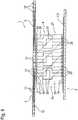
- the FIG. 1shows a test device 1 in a schematic representation, which has a conductor substrate 2, an electrical connection component 3, a contact-distance transformer 4 and a contact head 5. Furthermore, the test device 1 can have a receiving table 6 for a test object 7 to be tested for electrical functionality, wherein the test object 7 can be designed in particular as a wafer 8.
- the conductor substrate 2which is formed in particular as a multilayer printed circuit board, has on its upper side 9 outer edge contact surfaces 10, which are electrically connected via conductor tracks 11 lying on its underside 12 contact surfaces 13.
- the contact surfaces 13are in physical contact with contact springs 14 of the connection component 3.
- the connection component 3has a foil 15 which carries contact springs 14.
- the contact springs 14are in physical contact with first contacts 16 of the contact spacer transformer 4.
- the first contacts 16are located on a first side 17 of the contact spacer transformer 4.
- the buckling contact needles 21are longitudinally displaceably mounted in the guide bores 24 and 25, such that they stand with their one ends in touching contact with the second contacts 19 and protrude with their other ends of the guide plate 23 and thus are in contact with educalingstitleen 26 of the specimen 7 ,
- the Knick.nadeln 21are - as their name says - slightly laterally bent to develop a spring action.
- test circuitscan now be switched to the device under test 7, to check this for electrical functionality.
- This testis preferably carried out taking into account a large temperature spectrum.
- the contact-distance transformer 4is preferably completely formed as a 3D printing member 27. It has an electrically non-conductive support structure 28, and the support structure 28 passing through and / or arranged on the support structure 28 electrical connections 20. These consist of electrically conductive material.
- the support structure 28 and the connectionsare each 3D printed components 27.
- FIGS. 2a . 2 B . 3 . 4 and 5illustrate the manufacturing process of the contact distance transformer 4, which is created in the 3D printing process.
- FIG. 2ais printed on a substrate 29 by means of a non-illustrated 3D printer printing material 30 and 31 printed material in particular in layers and per layer in particular areas / printed.
- the printing materials 30 and 31are preferably located in dosing heads 32 and 33 of the 3D printer. These dosing heads 32 and 33 can be moved into corresponding spatial positions in order to eject or not eject the printing material 30, 31.
- On the underlay 29 located portion 34 of the emerging in the formation contact-distance transformer 4has a total of five layers 35 to 39.
- the individual layers 35 to 39consist of the printing material 30 and / or in the printing material 31.
- the printing material 30is electrically non-conductive and serves to produce the support structure 28 and the printing material 33 is electrically conductive and serves to produce the first contacts 16, second contacts 19, electrical connections 20 and / or cross connections 40.
- the cross connections 40belong to the connections 20.
- the connections 20enforce in predetermined (according to the applied software for the printing process of the 3D printer) webs horizontally, vertically and / or obliquely, ie 3D-moderate, the support structure 28th
- FIG. 2bis a section of FIG. 2a on a larger scale shows.
- the dosing heads 32 and 33are approached desired positions while doing the respective printing operation.
- the region 41is first produced by applying printing material 30.
- the printing operation of the dosing head 32is stopped and further printed with the dosing head 33 to produce the area 42 of printing material 31.
- an area 43 of printing material 30 in the layer 35ie the printing process is continued with the dosing head 32.
- the corresponding regions of the layer 36are printed on corresponding regions of the layer 35, so that either the electrically non-conductive section is increased or the electrically conductive section is enlarged or a transition is created from electrically conductive to electrically non-conductive or vice versa.
- the region 49produces an electrical connection 20 to the region 42.
- Region 44which is electrically conductive, is covered by electrically non-conductive region 50.
- Third layer 37which is printed on second layer 36, has a region 53 of electrically non-conductive printing material 30, a region 54 of electrically conductive material 31 and a region 55 of electrically non-conductive printing material 30. From the FIG.
- the region 49causes the region 49 to be electrically contacted with the region 54 and this in turn is electrically contacted with the region 51.
- the region 54forms a connection 20 formed as a cross-connection 40, which is electrically insulated by the region 50 from the region 44.
- the next layer 38has a region 56 of electrically non-conductive printing material 30, a region 57 of electrically conductive printing material 31 and a region 58 of electrically non-conductive printing material 30.
- the region 57is electrically connected to the region 54.
- the subsequent layer 39which is still being processed, consists - as can be seen - of non-conductive printing material 30, which is being delivered by the dosing head 32. Further layers can follow.
- the FIG. 3illustrates a manufacturing process of a contact-distance transformer 4, is operated in the same way as to the FIGS. 2a and 2 B described.
- at least one electrical component 59is printed during 3D printing.
- the 3D printeron the one hand on the previously described dosing heads 32 and 33 in order to apply electrically non-conductive printing material 30 and electrically conductive printing material 31.
- at least one additional dosing headis present.
- three additional dosing heads 60, 61 and 62are provided.
- the dosing 60is printed material of low electrical conductivity, that is, a conductivity to print electrical resistance paths.
- the dosing head 61has a printing material with a dielectric constant ⁇ 1.
- the dosing head 62has a printing material with a dielectric constant ⁇ 2.
- a sub-area of a contact distance transformer 4has already been made there, which - embedded in non-conductive printing material 30 - both second contacts 19 and electrical connections 20 and cross connections 40 has.
- the cross connections 40represent a subgroup of the connections 20.
- the second contacts 19are printed in such a way that they do not differ in terms of their spatial dimensions from the connections 20, but rather the connections 20 extend to the outside of the contact distance transformer 4, so that their end faces are available for touching contact.
- the end sections of the connections 20then form the contacts 19.
- FIG. 3shows that electrically less conductive printing material 63 was placed by means of the dosing head 60 between two second contacts 19 to generate an electrical resistance 64.
- an electrical component 59 in the form of the mentioned electrical resistance 64is created.
- capacitors 65printing material 66 and 67 corresponding to corresponding second contacts 19 has been printed by means of the dosing heads 61 and 62, wherein the printing materials 66 and 67 comprise different dielectric constants, thereby influencing the sizes of the capacitances of the capacitors.
- electrical components 59 inductorsdo not have - as from FIG. 3 visible - be placed on the outside, but they can also be embedded in the support structure 28.
- FIG. 4shows a further embodiment with respect to the production of the contact distance transformer 4 by means of 3D printing method.
- the arrangementcorresponds to the arrangement of FIG. 3 , so reference is made.
- 32 printed material 30is "printed" by means of a symbolically indicated dosing head, which is very thin and distributed as a result of the thin liquid by gravity and created in this way at least portions of the support structure 28.
- this low-viscosity printing material 30solidifies a short time after its printing.
- sealing walls 68are constructed laterally of the pressure structure and are only required until the printing material 30 has cured. After the completion of the 3D printed contact distance transformer 4, this is taken from the trough-shaped support structure (base 29 and sealing walls 68).
- the FIG. 5shows an embodiment according to the FIG. 4
- the printing with low-viscosity printing material 30 for the creation of electrically non-conductive areasSince, as already explained, layer-by-layer 3D printing takes place, separated regions may have to be filled individually by means of low-viscosity printing material 30 in order to overcome boundary structures 69, which in the present case are formed by electrical connections 20.
- the dosing head 32is used sequentially at three different positions, as shown in the FIG. 5 is hinted at.
- stiffenersare embedded to give the finished product a higher rigidity. These may be, for example, stiffening ribs or gratings and so on. These stiffeners are embedded by 3D printing accordingly. Of course it is also possible to create the stiffening elements by 3D printing.
- the FIG. 6shows a contact distance transformer 4, which is only partially created in the 3D printing process, namely only the middle area marked 70.
- a closing element 71 or 72was fixed, in particular secured by gluing.
- the end element 70is a ceramic plate 73 provided with mating holes 75 drilled with a cutting tool, these mating holes having the contact distance a.
- the end member 72is also a ceramic plate 74 provided with laser drilled mating holes 76, the individual mating holes 76 having a contact distance b from each other.
- the mating holes 75 and 76are provided with vias 77 to create electrical conductors.
- FIGS. 7 to 9show further embodiments of the invention, in which members of the test device are created in the 3D printing process, wherein the members can not only be the contact-distance transformer 4, but also other members, as will be explained below by way of example.
- the FIG. 7shows a created in 3D printing member 78, which - in comparison with the FIG. 1 -
- the conductor substrate 2, the connecting member 3 and the contact-distance transformer 4integrally includes.
- the 3D printed contact surfaces 10are arranged on the first side 17 of the member 78, preferably completely made in 3D printing, from which electrical connections 20 lead to the second side 18, on which the second contacts 19 rest, which are in contact with the contact head 5 be in touch contact.
- the member 68takes both the contact distance transformation of the conductor substrate 2 and the contact distance transformer 4.
- FIG. 8presents a member 79 created in 3D printing and the function of the contact spacer transformer 4 and the contact head 5 has integrated by - compared to the FIG. 1 -
- the contact-distance transformer 4 on its second side 18 in 3D printingraised printed contact elements 80 which come into contact with the contact DUT contacts 26 of the DUT 7 in its electrical testing.
- the structure of the embodimentcorresponds to FIG. 8 the structure of the embodiment of FIG. 1 ,
- the FIG. 9shows a highly integrated member 81, which is preferably completely created in 3D printing, and the functions of the conductor substrate 2, the connecting member 3, the contact-distance transformer 4 and the contact head 5 according to the embodiment of FIG. 1 integrated in itself. Accordingly, the 3D printed contact surfaces 10 are arranged on the first side 17 and raised contact elements 80 on the second side 18 in order to be able to contact the test object 7 there by electrical contact.
- electrical components 59are integrated in some compounds by 3D printing, namely electrical resistors R, coils L and capacitors C. Of course, these 3D printing components in all in the FIGS. 1 to 9 illustrated embodiments of the invention be integrated.
- FIGS. 1 to 9can only show two-dimensional structures. In fact, these structures are of course three-dimensional.
Landscapes
- Engineering & Computer Science (AREA)
- Microelectronics & Electronic Packaging (AREA)
- Physics & Mathematics (AREA)
- General Physics & Mathematics (AREA)
- Manufacturing & Machinery (AREA)
- Computer Hardware Design (AREA)
- Chemical & Material Sciences (AREA)
- Materials Engineering (AREA)
- Condensed Matter Physics & Semiconductors (AREA)
- Power Engineering (AREA)
- Measuring Leads Or Probes (AREA)
Description
Translated fromGermanDie Erfindung betrifft einen Kontakt-Abstandstransformer einer elektrischen Prüfeinrichtung zur Prüfung eines elektrischen Prüflings, insbesondere Wafers. Ferner betrifft die Erfindung eine elektrische Prüfeinrichtung zur Prüfung eines elektrischen Prüflings, insbesondere Wafers, mit einem Kontakt-Abstandstransformer. Schließlich betrifft die Erfindung ein Verfahren zur Herstellung eines Kontakt-Abstandstransformers einer elektrischen Prüfeinrichtung zur Prüfung eines elektrischen Prüflings, insbesondere Wafers.The invention relates to a contact-distance transformer of an electrical test device for testing an electrical test specimen, in particular wafer. Furthermore, the invention relates to an electrical test device for testing an electrical device under test, in particular wafer, with a contact distance transformer. Finally, the invention relates to a method for producing a contact-distance transformer of an electrical test device for testing an electrical test specimen, in particular wafer.
Aus der Offenlegungsschrift
Der erfindungsgemäße Kontakt-Abstandstransformer gehört einer elektrischen Prüfeinrichtung zur Prüfung eines elektrischen Prüflings, insbesondere Wafers, an. Diese elektrische Prüfeinrichtung, die ebenfalls Gegenstand der Erfindung ist, weist vorzugsweise ein Leitersubstrat, insbesondere eine Leiterplatte (PCB) auf, das/die bevorzugt mit Leiterbahnen versehen ist. Die Leiterbahnen führen auf einer Seite des Leitersubstrats insbesondere über Kabel zu einer Testeinrichtung (Tester). Auf der anderen Seite des Leitersubstrats liegen mit den Leiterbahnen verbundene Kontaktflächen, die über ein Verbindungsbauteil (Interposer) mit dem hier genannten Kontakt-Abstandstransformer elektrisch verbunden sind. Diese Verbindung erfolgt durch Berührungskontaktieren. Der Kontakt-Abstandstransformer setzt die Kontaktabstände des Leitersubstrats auf ein erheblich kleineres Maß um, d.h., der Kontakt-Abstandstransformer stellt Kontakte mit sehr geringem Abstand zur Verfügung, vorzugsweise einem Abstand der dem Kontaktabstand des Prüflings entspricht. Über einen Kontaktkopf, der vorzugsweise mindestens zwei beabstandet zueinander liegende, mit Führungsbohrungen versehene Führungsplatten aufweist, wobei in den Führungsbohrungen Knickkontaktnadeln lagern, werden die engliegenden Kontakte des Kontakt-Abstandstransformer in Berührungskontaktierung mit dem Prüfling verbunden. Mittels des Testers können somit Stromwege geschaltet werden, um die elektrische Funktionsfähigkeit des Prüflings zu testen. Neben dem vorstehend erläuterten Aufbau einer elektrischen Prüfeinrichtung umfasst die Erfindung auch andere Aufbauten, auf die nachstehend eingegangen wird. Die einzelnen, erwähnten Bauglieder, wie Leitersubstrat, Verbindungsbauteil, Kontakt-Abstandstransformer, Kontaktkopf und so weiter sind bei bekannten Prüfeinrichtungen in konventioneller Bauart erstellt.The contact distance transformer according to the invention belongs to an electrical test device for testing an electrical device under test, in particular a wafer. This electrical test device, which is also the subject of the invention, preferably has a conductor substrate, in particular a printed circuit board (PCB), which is / are preferably provided with conductor tracks. The conductor tracks lead on one side of the conductor substrate in particular via cables to a test device (tester). On the other side of the conductor substrate are connected to the conductor tracks contact surfaces, which are electrically connected via a connection component (Interposer) with the contact spacer transformer mentioned here. This connection is made by touch contact. The contact spacer transforms the contact distances of the conductor substrate to a much smaller extent, that is, the contact spacer transforms contacts at a very close spacing Available, preferably a distance corresponding to the contact distance of the specimen. Via a contact head, which preferably has at least two mutually spaced, provided with guide holes guide plates, store in the guide holes buckling needles, the engliegenden contacts of the contact distance transformer are in touch contact with the DUT connected. By means of the tester, current paths can thus be switched in order to test the electrical functionality of the test object. In addition to the above-described construction of an electrical testing device, the invention also includes other structures, which will be discussed below. The individual components mentioned, such as conductor substrate, connection component, contact distance transformer, contact head and so on are created in conventional test equipment in conventional design.
Der Erfindung liegt die Aufgabe zugrunde, mindestens ein Bauglied einer Prüfeinrichtung, insbesondere einen Kontakt-Abstandstransformer, anzugeben, das/der einfach aufgebaut und preiswert ist, insbesondere auch in sehr kurzer Zeit hergestellt werden kann. Gegenüber einem bekannten Kontakt-Abstandstransformer, der aus mehrlagiger Keramik aufgebaut ist, wobei die Keramik mit Leiterbahnen versehene Keramikplatten aufweist und derartige Keramikplatten Lage um Lage aufeinandergestapelt und zusammengepresst und dabei gesindert werden, soll also ein wesentlich einfacher und kostengünstiger aufgebautes Bauglied geschaffen werden. Ferner soll auch eine entsprechend einfache und kostengünstig aufgebaute elektrische Prüfeinrichtung geschaffen werden sowie ein Verfahren, um zu derartigen erfindungsgemäßen Kontakt-Abstandstransformern (Spacetransformern) beziehungsweise Prüfeinrichtungen zu gelangen.The invention has for its object to provide at least one member of a test device, in particular a contact distance transformer, the / is simple in construction and inexpensive, in particular can be produced in a very short time. Compared to a known contact distance transformer, which is constructed of multilayer ceramic, wherein the ceramic has conductor tracks provided with ceramic plates and such ceramic plates stacked layer by layer and pressed together and thereby be reduced, so a much simpler and less expensive constructed member should be created. Furthermore, a correspondingly simple and inexpensive constructed electrical test device should be created as well as a method to such according to the invention Contact distance transformers (Spacetransformern) or testing facilities to get.
Diese Aufgabe wird bei einem Kontakt-Abstandstransformer einer elektrischen Prüfeinrichtung zur Prüfung eines elektrischen Prüflings, insbesondere Wafers, dadurch gelöst, dass der Kontakt-Abstandstransformer zur Abstandsverkleinerung von benachbart zueinander liegenden elektrischen Kontakten eine elektrisch nichtleitende Tragstruktur aufweist, die eine erste Seite und eine zweite Seite besitzt, wobei auf der ersten Seite erste elektrische Kontakte mit einem Kontaktabstand zueinander liegen und auf der zweiten Seite zweite elektrische Kontakte angeordnet sind, die einen gegenüber den ersten Kontakten der ersten Seite kleineren Kontaktabstand zueinander aufweisen, wobei die ersten Kontakte mit den zweiten Kontakten mittels die Tragstruktur durchsetzenden und/oder auf der Tragstruktur angeordneten elektrischen Verbindungen verbunden sind, wobei sowohl die Tragstruktur als auch die elektrischen Verbindungen als 3D-Druckbauteile ausgebildet sind. Demzufolge sind die Tragstruktur und die elektrischen Verbindungen im 3D-Drucker-Fügeverfahren erstellt. Da die Tragstruktur elektrisch nichtleitend ausgebildet ist, wird für den 3D-Druck elektrisch isolierendes Druckmaterial verwendet. Für die elektrischen Verbindungen wird dementsprechend beim 3D-Druck elektrisch leitendes Druckmaterial eingesetzt. Beim 3D-Druck werden die genannten Druckmaterialien vorzugsweise mit entsprechenden Dosierköpfen appliziert. Entsprechend einem 3D-Drucker fahren die Dosierköpfe, in denen sich das zugehörige Fügematerial (Druckmaterial) befindet, an entsprechende Positionen und dabei/dann wird das Druckmaterial ausgestoßen, sodass es - verfestigt - entsprechende Teile der Tragstruktur beziehungsweise der elektrischen Verbindungen aufbaut. Dabei wird vorzugsweise schrittweise vorgegangen, wenn beispielsweise auf einem Tragstrukturbereich ein elektrischer Verbindungsbereich aufgetragen werden soll, so ist der Tragstrukturbereich Voraussetzung für die darauf erfolgende Erzeugung des elektrischen Verbindungsbereichs, sodass zunächst dieser Tragstrukturbereich gedruckt werden muss und erst danach der elektrischen Verbindungsbereich. Vorzugsweise können dieselben und/oder die verschiedenen Druckmaterialien schichtweise aufgetragen werden. Selbstverständlich ist es möglich, dass im Zuge des 3D-Druckverfahrens Versteifungselemente zugeführt und "umdruckt" werden, um der Gesamtanordnung eine höhere Festigkeit zu verleihen. Überdies können, vorzugsweise ebenfalls im 3D-Druck, Klebstoffe, insbesondere leitfähige Klebstoffe, und Füllstoffe, insbesondere isolierende Füllstoffe, zugeführt, also gedruckt werden. Aufgrund der Erfindung lässt sich demzufolge ein Kontakt-Abstandstransformer im 3D-Druckverfahren erstellen, was sehr kostengünstig ist und zur schnellen Verfügbarkeit des fertigen Produktes führt. Komplizierteste Strukturen der elektrischen Verbindungen lassen sich flächig und räumlich auf und/oder in der Tragstruktur erstellen. Der 3D-Druck ermöglicht es, die elektrischen Verbindungen auf der zweiten Seite der nichtleitenden Tragstruktur gegenüber deren Anordnung auf der ersten Seite derart stark zu "bündeln", dass die gewünschte Kontakt-Abstandsverkleinerung erzielt wird.This object is achieved in a contact distance transformer of an electrical test device for testing an electrical test specimen, in particular wafer, characterized in that the contact distance transformer for reducing the distance of adjacent electrical contacts has an electrically non-conductive support structure having a first side and a second side has, wherein on the first side first electrical contacts with a contact distance to each other and on the second side second electrical contacts are arranged, which have a relation to the first contacts of the first side smaller contact distance to each other, wherein the first contacts with the second contacts by means of Support structure passing through and / or arranged on the support structure electrical connections are connected, wherein both the support structure and the electrical connections are formed as 3D printing components. As a result, the support structure and the electrical connections are created in the 3D printer joining method. Since the support structure is electrically non-conductive, electrically insulating printing material is used for 3D printing. Accordingly, electrically conductive printing material is used for the electrical connections in 3D printing. In the case of 3D printing, the printing materials mentioned are preferably applied with appropriate dosing heads. According to a 3D printer, the dosing heads, in which the associated joining material (printing material) is located, move to corresponding positions and / or the printing material is ejected, so that it-solidified-builds up corresponding parts of the supporting structure or of the electrical connections. It is preferred proceeding stepwise, if, for example, an electrical connection region is to be applied to a support structure region, then the support structure region is a prerequisite for the subsequent generation of the electrical connection region, so that first this support structure region must be printed and only then the electrical connection region. Preferably, the same and / or the different printing materials can be applied in layers. Of course, it is possible that in the course of the 3D printing process stiffening elements supplied and "reprinted" to give the overall arrangement a higher strength. Moreover, preferably also in 3D printing, adhesives, in particular conductive adhesives, and fillers, in particular insulating fillers, can be supplied, ie printed. As a result of the invention, a contact distance transformer can be produced in the 3D printing process, which is very cost-effective and leads to rapid availability of the finished product. The most complicated structures of the electrical connections can be created flat and spatially on and / or in the supporting structure. The 3D printing makes it possible to "bundle" the electrical connections on the second side of the non-conductive support structure in relation to their arrangement on the first side so strongly that the desired contact distance reduction is achieved.
Nach einer Weiterbildung der Erfindung ist vorgesehen, dass die ersten und/oder die zweiten Kontakte ebenfalls als 3D-Druckbauteile ausgebildet sind. Diese an der ersten beziehungsweise an der zweiten Seite der Tragstruktur liegenden Kontakte können vorzugsweise mit dem gleichen Druckmaterial und dem gleichen Dosierkopf erstellt werden, wie auch die elektrischen Verbindungen.According to a development of the invention it is provided that the first and / or the second contacts are also formed as 3D-printing components. These lying on the first and on the second side of the support structure contacts can preferably be created with the same printing material and the same dosing, as well as the electrical connections.
Nach einer Weiterbildung der Erfindung ist vorgesehen, dass mindestens ein erster und/oder mindestens ein zweiter Kontakt durch die Stirnfläche mindestens einer der elektrischen Verbindungen gebildet ist. Die Kontakte sind insofern nicht gestalterisch unterschiedlich zu den zugehörigen Verbindungen, sondern die jeweilige Verbindung verläuft bis an die erste oder zweite Seite der Tragstruktur, sodass von außen betrachtet nur die Stirnfläche dieser Verbindung ersichtlich ist, wobei diese Stirnfläche den entsprechenden Kontakt bildet.According to a development of the invention, it is provided that at least one first and / or at least one second contact is formed by the end face of at least one of the electrical connections. The contacts are insofar not structurally different from the associated compounds, but the respective connection extends to the first or second side of the support structure, so viewed from the outside, only the end face of this connection is visible, said end face forms the corresponding contact.
Besonders vorteilhaft ist es, wenn der Kontakt-Abstandstransformer nur aus 3D-Druckbauteilen besteht. Demzufolge wird er komplett im 3D-Druckverfahren erstellt.It is particularly advantageous if the contact spacer transformer consists only of 3D printed components. As a result, it is completely created in 3D printing.
Nach einer Weiterbildung der Erfindung ist vorgesehen, dass der Kontakt-Abstandstransformer mindestens ein elektrisches Bauelement, insbesondere einen Widerstand, eine Spule und/oder einen Kondensator, aufweist, wobei das Bauelement ebenfalls als 3D-Druckbauteil ausgebildet ist. Diese verschiedenen Bauelemente werden demgemäß während des 3D-Drucks des Kontakt-Abstandstransformers miterzeugt. Hierzu ist ein Dosierkopf vorhanden, der beispielsweise ein Druckmaterial enthält, das als Widerstandsmaterial für einen elektrischen Widerstand verwendet werden kann. Spulen werden dadurch erzeugt, dass ein Druckkopf eine spiralförmige Druckbahn herstellt und elektrisch leitfähiges Druckmaterial verwendet wird. Kondensatoren lassen sich im 3D-Druck dadurch erzeugen, dass einander gegenüberstehende Leiter/Elektroden gedruckt werden. Hierbei kann zwischen die Leiter/Elektroden wiederum ein elektrisch nichtleitendes Druckmaterial mittels eines entsprechenden Dosierkopfes aufgetragen werden, wobei das Druckmaterial bevorzugt eine gewünschte Dielektrizitätskonstante aufweist.According to a development of the invention, it is provided that the contact-distance transformer has at least one electrical component, in particular a resistor, a coil and / or a capacitor, wherein the component is likewise designed as a 3D-printing component. These various components are accordingly generated during the 3D printing of the contact spacer transformer. For this purpose, a dosing head is provided which contains, for example, a printing material which can be used as a resistance material for an electrical resistance. Coils are created by making a printhead a helical printing web and using electrically conductive printing material. Capacitors can be created in 3D printing by printing opposing conductors / electrodes. In this case, an electrically non-conductive printing material can in turn be applied by means of a corresponding dosing head between the conductors / electrodes, wherein the printing material preferably has a desired dielectric constant.
Vorzugsweise ist vorgesehen, dass das mindestens eine elektrische Bauelement an mindestens einem der ersten Kontakte, einem der zweiten Kontakte und/oder einer der Verbindungen durch eine elektrisch leitfähige 3D-Druckkontaktstelle elektrisch angeschlossen ist.It is preferably provided that the at least one electrical component is electrically connected to at least one of the first contacts, one of the second contacts and / or one of the connections by an electrically conductive 3D pressure contact point.
Um eine Hybridbauweise, bevorzugt eine Sandwichbauweise, bei dem Kontakt-Abstandstransformer zu realisieren, ist bevorzugt auf der ersten Seite und/oder der zweiten Seite ein Abschlusselement, insbesondere eine Abschlussplatte, bevorzugt eine Keramikplatte, angeordnet, insbesondere befestigt, wobei das Abschlusselement kein 3D-Druckbauteil ist. Bevorzugt können zwei Keramikplatten vorgesehen sein, zwischen denen der im 3D-Druck erzeugte Bereich des Kontakt-Abstandstransformers liegt, wobei die beiden Keramikplatten mit Durchgangskontakten, insbesondere Durchkontaktierungen, versehen sind, die mit den ersten beziehungsweise zweiten Kontakten elektrisch verbunden sind. Die Durchgangskontaktanordnung der einen Keramikplatte weist einen der ersten Kontakte entsprechenden Kontaktabstand auf und der Kontaktabstand der Durchgangskontakte, insbesondere Durchkontaktierungen, der anderen Keramikplatte ist entsprechend kleiner gewählt (wie der der zweiten Kontakte), um die Kontaktabstandsumsetzung (Spacetransformerfunktion) zu erzielen.In order to realize a hybrid construction, preferably a sandwich construction, in the contact spacer transformer, a termination element, in particular a termination plate, preferably a ceramic plate, is preferably arranged, in particular fastened, on the first side and / or the second side, the termination element not having a Pressure member is. Preferably, two ceramic plates may be provided, between which the area of the contact distance transformer generated in 3D printing is located, wherein the two ceramic plates are provided with through contacts, in particular plated-through holes, which are electrically connected to the first and second contacts. The via contact arrangement of the one ceramic plate has a contact spacing corresponding to the first contacts, and the contact spacing of the via contacts, in particular vias, of the other ceramic plate is selected to be correspondingly smaller (such as that of the second contacts) to achieve the contact pitch translation (Spacetransformerfunktion).
Die Erfindung betrifft ferner eine elektrische Prüfeinrichtung zur Prüfung eines elektrischen Prüflings, insbesondere Wafers, wobei ein Kontakt-Abstandstransformer verwendet wird, der entsprechend mindestens einer der vorstehend genannten Ausführungen ausgestaltet ist.The invention further relates to an electrical test device for testing an electrical test specimen, in particular wafer, wherein a contact distance transformer is used, the corresponding at least one of the aforementioned embodiments is configured.
Nach einer Weiterbildung der elektrischen Prüfeinrichtung ist vorgesehen, dass diese ein Leitersubstrat mit Kontaktflächen besitzt, die mit den ersten Kontakten des Kontakt-Abstandstransformers direkt oder über ein elektrisches Verbindungsbauteil in elektrischer Verbindung, bevorzugt elektrischer Berührungsverbindung, steht. Das Verbindungsbauteil ist vorzugsweise in konventioneller Technik, also nicht in 3D-Drucktechnik erstellt.According to a development of the electrical testing device is provided that this has a conductor substrate with contact surfaces, which is directly connected to the first contacts of the contact-distance transformer or via an electrical connection component, preferably electrical contact connection. The connection component is preferably created in conventional technology, that is not in 3D printing technology.
Bevorzugt weist das Verbindungsbauteil eine mit Kontaktfedern bestückte Folie auf. Mittels der Kontaktfedern werden einerseits die Kontaktflächen des Leitersubstrats berührungskontaktiert und andererseits die ersten Kontakte des 3D-Druck-Kontakt-Abstandstransformers.The connecting component preferably has a foil fitted with contact springs. By means of the contact springs, the contact surfaces of the conductor substrate are contact-contacted on the one hand and, on the other hand, the first contacts of the 3D pressure-contact distance transformer.
Nach einer Weiterbildung der elektrischen Prüfeinrichtung ist ein Kontaktkopf vorgesehen, der Kontaktbauteile für eine elektrische Berührungskontaktierung des Prüflings aufweist. Die Anordnung ist dabei vorzugsweise derart getroffen, dass das Leitersubstrat, insbesondere wie vorstehend beschrieben, mit dem Kontakt-Abstandstransformer in elektrischer Verbindung steht und dass der Kontakt-Abstandstransformer in elektrischer Verbindung mit der einen Seite des Kontaktkopfs, insbesondere mit den Kontaktbauteilen des Kontaktkopfs in elektrischer Verbindung steht, wobei der Kontaktkopf eine elektrische Berührungskontaktierung mit Kontakten des Prüflings vornimmt. Diese elektrische Berührungskontaktierung wird bevorzugt von den Kontaktbauteilen des Kontaktkopfs vorgenommen.According to a development of the electrical test device, a contact head is provided which has contact components for electrical contact contacting of the test object. The arrangement is preferably made such that the conductor substrate, in particular as described above, is in electrical connection with the contact spacer transformer and that the contact spacer transformer in electrical connection with the one side of the contact head, in particular with the contact components of the contact head in electrical Connection is made, wherein the contact head makes an electrical contact contacting with contacts of the test specimen. This electrical contact contacting is preferably carried out by the contact components of the contact head.
Vorzugsweise ist bei der elektrischen Prüfeinrichtung vorgesehen, dass die Kontaktbauteile als Knickkontaktnadeln, Federkontaktstifte, Pogos oder dergleichen ausgebildet sind. Die Knickkontaktnadeln können sich bei der Kontaktierung elastisch durchbiegen, also seitlich ausknicken. Die Federkontaktstifte können insbesondere derart ausgebildet sein, dass sie ein federkraftbeaufschlagtes Kontaktelement besitzen, beispielsweise einen in einer Hülse verschieblich gelagerten Kolben, der eine Kontaktspitze aufweist, wobei der Kolben von einer Feder, insbesondere Schraubendruckfeder beaufschlagt wird. Die als Pogos bezeichneten Kontaktbauteile sind ebenfalls federnde Kontakte, insbesondere Federkontaktstifte, wobei der Begriff "Pogos" insbesondere in den USA Verwendung findet.Preferably, it is provided in the electrical test device that the contact components are designed as buckling contact needles, spring contact pins, Pogos or the like. The buckling contact needles can bend elastically during contacting, ie buckle laterally. The spring contact pins may in particular be designed such that they have a spring-loaded contact element, for example a displaceably mounted in a sleeve piston having a contact tip, wherein the piston is acted upon by a spring, in particular helical compression spring. The designated as Pogos contact components are also resilient contacts, especially spring contact pins, the term "Pogos" is used especially in the US.
Ferner weist die elektrische Prüfeinrichtung - nach einer Weiterbildung der Erfindung - bevorzugt den Kontaktkopf auf, der mindestens zwei beabstandet zueinander liegende, mit Führungsbohrungen versehene Führungsplatten besitzt, wobei in den Führungsbohrungen die Kontaktbauteile, insbesondere Knickkontaktnadeln, für eine elektrischen Berührungskontaktierung des Prüflings liegen/lagern. Die insbesondere vorgesehenen Knickkontaktnadeln können bei der Kontaktierung des Prüflings seitlich ausfedern, wodurch eine sichere Kontaktierung gewährleistet ist. Der Kontaktkopf ist in konventioneller Technik hergestellt. Die Knickkontaktnadeln sind in den Führungsbohrungen der Führungsplatten längsverschieblich gelagert, um eine gute Kontaktierung einerseits zu dem Kontakt-Abstandstransformer und andererseits zu dem Prüfling zu erzielen.Further, the electrical test device - according to a development of the invention - preferably on the contact head, which has at least two mutually spaced, provided with guide holes guide plates, in the guide holes, the contact components, in particular buckling needles, for electrical contact contacting the test specimen lie / store. The particular provided Knickkontaktnadeln can spring laterally when contacting the test specimen, whereby a secure contact is ensured. The contact head is manufactured using conventional technology. The buckling contact needles are longitudinally displaceably mounted in the guide bores of the guide plates in order to achieve a good contact on the one hand to the contact distance transformer and on the other hand to the DUT.
Eine Weiterbildung der Erfindung sieht vor, dass die Kontaktbauteile, insbesondere Knickkontaktnadeln, mit ihren einen Enden in Berührungskontakt mit den zweiten Kontakten des Kontakt-Abstandstransformers stehen. Hierauf wurde vorstehend bereits eingegangen.A development of the invention provides that the contact components, in particular buckling contact needles, with their one ends in touching contact with the second contacts of the contact Abstandstransformers stand. This has already been discussed above.
Eine Weiterbildung der Erfindung sieht vor, dass der Kontakt-Abstandstransformer das Leitersubstrat mitausbildet. Demzufolge ist Leitersubstrat und Kontakt-Abstandstransformer in einem Bauteil zusammengefasst, wobei das gesamte Bauteil im 3D-Druck erstellt ist.A development of the invention provides that the contact spacer transforms the conductor substrate. As a result, the conductor substrate and the contact spacer transformer are combined in one component, the entire component being produced in 3D printing.
Bevorzugt kann vorgesehen sein, dass die zweiten Kontakte des Kontakt-Abstandstransformers im 3D-Druck gedruckte, insbesondere erhaben gedruckte Kontaktelemente zum direkten Berührungskontaktieren des Prüflings sind. Bei dieser Ausführungsform benötigt die Prüfeinrichtung demzufolge keinen Kontaktkopf.It can preferably be provided that the second contacts of the contact distance transformer are printed in 3D printing, in particular raised printed contact elements for the direct contact contacting of the test object. Consequently, in this embodiment, the test device does not require a contact head.
Bevorzugt kann ferner vorgesehen sein, dass die Kontaktelemente als punktförmige Kontakte, in Berührungskontaktierungsrichtung stiftförmige Kontakte oder größtenteils quer zur Berührungskontaktierungsrichtung verlaufende Kontakte, insbesondere Cantilever-Kontakte, ausgebildet sind. Die punktförmigen Kontakte sind hinsichtlich ihrer Form etwa ebenso lang wie breit ausgebildet. Die in Berührungskontaktierungsrichtung stiftförmigen Kontakte haben in Berührungskontaktierungsrichtung eine größere Ausdehnung als quer dazu. Die größtenteils quer zu ihrer Berührungskontaktierungsrichtung verlaufenden Kontakte, insbesondere Cantilever-Kontakte, sind derart gestaltet, dass sie einen Abschnitt aufweisen, der quer zur Berührungskontaktierungsrichtung verläuft, wobei unter quer sowohl schräg, als auch rechtwinklig zu verstehen ist. Ferner weisen sie vorzugsweise einen von diesem quer verlaufenden Abschnitt abgewinkelt verlaufenden Bereich auf, mit dem die Berührungskontaktierung des Prüflings erfolgt. Insbesondere der quer verlaufende Abschnitt führt zu einer Federwirkung, also einem elastischen Nachgeben bei der Berührungskontaktierung.Preferably, it can further be provided that the contact elements are designed as punctiform contacts, pin-shaped contacts in the contact-contacting direction, or contacts, in particular cantilever contacts, which run largely transversely to the contact-contacting direction. The punctiform contacts are approximately as long as wide in shape. The contact-pin-shaped contacts have a greater extent in the contact-contacting direction than in the transverse direction. The mostly transverse to their contact contacting direction extending contacts, in particular cantilever contacts, are designed such that they have a portion which extends transversely to the Kontaktungskontaktierungsrichtung, wherein transverse is to be understood both obliquely, as well as at right angles. Furthermore, they preferably have an area extending at an angle from this transverse section, with which the contact contacting of the test object takes place. In particular, the transverse section leads to a spring effect, ie an elastic yielding in the touch contact.
Die Erfindung betrifft ferner ein Verfahren zur Herstellung eines Kontakt-Abstandstransformers einer elektrischen Prüfeinrichtung zur Prüfung eines elektrischen Prüflings, insbesondere Wafers, wobei der Kontakt-Abstandstransformer insbesondere gemäß einer der vorstehenden Ausführungen ausgebildet ist/wird, wobei folgende Schritte vorgesehen sind: 3D-Drucken, insbesondere schichtweises 3D-Drucken, von einer Tragstruktur aus elektrisch isolierendem Druckmaterial sowie 3D-Drucken, insbesondere schichtweises 3D-Drucken, von die Tragstruktur durchsetzenden und/oder auf der Tragstruktur angeordneten elektrischen Verbindungen aus elektrisch leitfähigem Druckmaterial.The invention further relates to a method for producing a contact-distance transformer of an electrical test device for testing an electrical test specimen, in particular wafer, wherein the contact distance transformer is in particular formed according to one of the preceding embodiments, wherein the following steps are provided: 3D printing, in particular layered 3D printing, of a support structure of electrically insulating printing material and 3D printing, in particular layer-by-layer 3D printing, electrical connections made of electrically conductive printing material passing through the support structure and / or arranged on the support structure.
Insbesondere kann ein 3D-Drucken, insbesondere schichtweises 3D-Drucken, von ersten und/oder zweiten Kontakten aus elektrisch leitfähigem Druckmaterial erfolgen, wobei die ersten und/oder zweiten Kontakte an mindestens einem der Enden der elektrischen Verbindungen angeordnet werden. Sofern die ersten und/oder zweiten Kontakte nicht separat von den elektrischen Verbindungen ausgestaltet werden, sondern die elektrischen Verbindungen durch ihre Stirnflächen beziehungsweise Endbereiche die ersten und/oder zweiten Kontakte bilden, werden diese Kontakte bereits mit der Erstellung der elektrischen Verbindungen erzeugt.In particular, 3D printing, in particular layer-by-layer 3D printing, can take place from first and / or second contacts of electrically conductive printing material, wherein the first and / or second contacts are arranged on at least one of the ends of the electrical connections. If the first and / or second contacts are not configured separately from the electrical connections but the electrical connections form the first and / or second contacts through their end faces or end regions, these contacts are already generated when the electrical connections are made.
Insbesondere kann vorgesehen sein, dass ein 3D-Drucken, insbesondere schichtweises 3D-Drucken, erfolgt, um mittels elektrisch leitfähigem Druckmaterial auf zuvor 3D-gedruckten, elektrisch isolierendem Druckmaterial, bevorzugt elektrische Querverbindungen oder dergleichen, auch Diagonalverbindungen und so weiter, herzustellen.In particular, provision may be made for 3D printing, in particular layer-by-layer 3D printing, to be carried out by means of electrically conductive printing material on previously 3D-printed, electrically insulating Printing material, preferably electrical cross-links or the like, also diagonal connections and so on to produce.
Eine Weiterbildung des erfindungsgemäßen Verfahrens sieht ein 3D-Drucken vor, insbesondere ein schichtweises 3D-Drucken, um mittels elektrisch weniger leitfähigem Druckmaterial mindestens einen elektrischen Widerstand herzustellen. Derartige Widerstände liegen somit insbesondere im Innern des Kontakt-Abstandstransformers, vorzugsweise eingebettet in die 3D-gedruckte Tragstruktur. Entsprechendes gilt für den nachstehend erwähnten Kondensator beziehungsweise die nachstehend erwähnte Spule.A development of the method according to the invention provides 3D printing, in particular layer-by-layer 3D printing, in order to produce at least one electrical resistance by means of electrically less conductive printing material. Such resistors are thus in particular in the interior of the contact distance transformer, preferably embedded in the 3D printed support structure. The same applies to the capacitor mentioned below or the coil mentioned below.
Bevorzugt erfolgt ein 3D-Drucken, insbesondere schichtweises 3D-Drucken, von sich gegenüberliegenden Elektroden aus elektrisch leitfähigem Druckmaterial zur Herstellung eines Kondensators, wobei vorzugsweise ein 3D-Druck von Dielektrikummaterial zwischen die Elektroden erfolgt.Preferably, a 3D printing, in particular layer-by-layer 3D printing, of opposing electrodes made of electrically conductive printing material for the production of a capacitor, wherein preferably takes place a 3D printing of dielectric material between the electrodes.
Ferner ist bevorzugt ein 3D-Drucken, insbesondere schichtweises 3D-Drucken, von spiralförmigen und/oder schneckenförmigen und/oder wendelförmigen Leitern aus elektrisch leitfähigem Material zur Herstellung von mindestens einer Spule vorgesehen.Furthermore, 3D printing, in particular layer-by-layer 3D printing, of spiral-shaped and / or spiral-shaped and / or helical conductors of electrically conductive material is preferably provided for producing at least one coil.
Ferner ist das erfindungsgemäße Verfahren gekennzeichnet durch 3D-Drucken, insbesondere schichtweises 3D-Drucken, von flüssiger, sich unter Schwerkrafteinwirkung verteilender und danach aushärtender Isolierflüssigkeit zur Herstellung von elektrischen Isolierbereichen, insbesondere von Isolationsschichten. Hierbei handelt es sich bevorzugt um die Tragstruktur beziehungsweise Teile der Tragstruktur. Entsprechend kann auch elektrisch leitfähige Flüssigkeit gedruckt werden.Furthermore, the method according to the invention is characterized by 3D printing, in particular layer-by-layer 3D printing, of liquid, gravitationally distributing and then hardening insulating liquid for producing electrical insulating regions, in particular insulating layers. This is preferably the support structure or parts of the support structure. Accordingly, electrically conductive liquid can be printed.
Ferner kann bevorzugt vorgesehen sein, mittels 3D-Druck Kleb- und/oder Füllstoffe bei der Erstellung des Kontakt-Abstandstransformers oder der elektrischen Prüfeinrichtung beziehungsweise bei der Durchführung des erwähnten Verfahrens vorzusehen. Die Klebstoffe können elektrisch leitfähig oder elektrisch nicht leitfähig sein. Entsprechendes gilt für die Füllstoffe.Furthermore, it can preferably be provided to provide adhesives and / or fillers by means of 3D printing during the preparation of the contact spacer transformer or the electrical test device or during the implementation of the mentioned method. The adhesives may be electrically conductive or electrically nonconductive. The same applies to the fillers.
Die Zeichnungen veranschaulichen die Erfindung anhand von Ausführungsbeispielen und zwar zeigt:
- Figur 1
- eine schematische Darstellung einer Prüfeinrichtung zur Prüfung eines elektrischen Prüflings,
- Figur 2a
- einen 3D-Druckvorgang,
- Figur 2b
- eine Ausschnittvergrößerung aus
Figur 2a , Figuren 3bis 5- weitere 3D-Druckvorgänge,
Figur 6- eine schematische Querschnittsansicht durch einen Kontakt-Abstandstransformer,
Figur 7- eine Prüfeinrichtung nach einem weiteren Ausführungsbeispiel,
Figur 8- eine Prüfeinrichtung nach einem weiteren Ausführungsbeispiel und
Figur 9- eine Prüfeinrichtung nach einem letzten Ausführungsbeispiel.
- FIG. 1
- a schematic representation of a test device for testing an electrical specimen,
- FIG. 2a
- a 3D printing process,
- FIG. 2b
- a cutout enlargement
FIG. 2a . - FIGS. 3 to 5
- additional 3D printing processes,
- FIG. 6
- a schematic cross-sectional view through a contact distance transformer,
- FIG. 7
- a test device according to a further embodiment,
- FIG. 8
- a test device according to a further embodiment and
- FIG. 9
- a test device according to a last embodiment.
Die
Das Leitersubstrat 2, das insbesondere als mehrlagige Leiterplatte ausgebildet ist, weist auf seiner Oberseite 9 außenrandseitig liegende Kontaktflächen 10 auf, die über Leiterbahnen 11 mit an seiner Unterseite 12 liegenden Kontaktflächen 13 elektrisch verbunden sind. Die Kontaktflächen 13 stehen in Berührungskontaktierung mit Kontaktfedern 14 des Verbindungsbauteils 3. Das Verbindungsbauteil 3 weist eine Folie 15 auf, die Kontaktfedern 14 trägt. Die Kontaktfedern 14 stehen in Berührungskontaktierung mit ersten Kontakten 16 des Kontakt-Abstandstransformers 4. Die ersten Kontakte 16 befinden sich an einer ersten Seite 17 des Kontakt-Abstandstransformers 4. An einer zweiten Seite 18 des Kontakt-Abstandstransformers 4, die vorzugsweise der ersten Seite 17 planparallel gegenüberliegt, befinden sich zweite Kontakte 19 des Kontakt-Abstandstransformers 4, wobei die ersten Kontakte 16 mit den zweiten Kontakten 19 über elektrische Verbindungen 20 verbunden sind. Dabei können, entsprechend der Prüfung des Prüflings 7 komplizierte Verlaufsstrukturen der elektrischen Verbindungen 20 vorliegen, um entsprechende erste Kontakte 16 mit entsprechenden zweiten Kontakten 19 zu verbinden. Überdies ist vorgesehen, dass benachbart zueinander liegende erste Kontakte 16 einen Kontaktabstand a aufweisen und das benachbart zueinander liegende zweite Kontakte 19 einen Kontaktabstand b aufweisen. Die Anordnung ist nun so getroffen, dass der Kontaktabstand b sehr viel kleiner ist als der Kontaktabstand a, was - aus zeichentechnischen Gründen - jedoch nicht der
Für die Prüfung des elektrischen Prüflings 7 wird dieser mittels des Aufnahmetischs 6 angehoben und gegen die Prüfeinrichtung 1 gedrückt, wodurch die vorstehend genannten Berührungskontaktierungen der verschiedenen Bauglieder stattfindet. Über elektrische, nicht dargestellte Leitungen, die an die Kontaktflächen 10 angeschlossen sind und die zu einem Tester führen, können nun Prüfstromkreise zum Prüfling 7 geschaltet werden, um diesen auf elektrische Funktionsfähigkeit zu prüfen. Diese Prüfung erfolgt vorzugsweise auch unter Berücksichtigung eines großen Temperaturspektrums.For the test of the
Die erfindungsgemäße Anordnung der
Die
Zur Verdeutlichung des erwähnten schichtweisen und innerhalb jeder Schicht gegebenenfalls bereichsweise erfolgenden Druckens verschiedener Druckmaterialien 30, 31 wird auf die
Die
Die
Die
Insbesondere bei dünnflüssigem Druckmaterial 30 gemäß der
Ferner ist es - nach einer nicht dargestellten Weiterbildung der Erfindung - möglich, dass in das jeweilige Druckmaterial, beispielsweise in das nicht leitende Druckmaterial 30, Versteifungen eingebettet werden, um dem fertigen Produkt eine höhere Steifigkeit zu geben. Hierbei kann es sich beispielsweise um Versteifungsrippen oder Gitter und so weiter handeln. Diese Versteifungselemente werden durch das 3D-Drucken entsprechend eingebettet. Es ist natürlich auch möglich, die Versteifungselemente durch 3D-Drucken mit zu erstellen.Further, it is possible - according to a further embodiment of the invention, not shown - that in the respective printing material, for example, in the
Die
Die
Die
Das Ausführungsbeispiel der
Die
Alle erwähnten
Claims (17)
- A contact-distance transformer of an electric testing device for testing an electric specimen, in particular a wafer, wherein said contact-distance transformer is used to reduce the distance between neighbouring electric contacts, and is provided with a non-electrically conductive supporting structure, which is provided with a first side and a second side, wherein on the first side first electric contacts are positioned at a contact distance to each other, and on the second side second electric contacts are positioned, which have a contact distance to each other which is smaller than the contact distance of the first contacts on the first side, wherein the first contacts are connected to the second contacts by means of electric connections which pass through the support structure and/or which are positioned on the support structure,characterized in that both the support structure (28) and the electric connections (20) are formed as 3D-printed components (27).
- The contact-distance transformer according to claim 1,characterized in that the first and/or second contacts (16, 19) are also formed as 3D-printed components (27).
- The contact-distance transformer according to any of the preceding claims,characterized in that at least a first and/or at least a second contact (16, 19) are formed by the front surface of at least one of the electric connections (20).
- The contact-distance transformer according to any of the preceding claims,characterized in that on the first side (17) and/or on the second side (18) a terminal element (71), in particular a terminal plate, preferably a ceramic plate (73, 74), is positioned, in particular attached, wherein the terminal element (71) is not a 3D-printed component.
- The contact-distance transformer according to any of the preceding claims,characterized in that the terminal element (71) is provided with through contacts, in particular through-hole platings (77), which are electrically connected to the first or second contacts (16, 19).
- An electric testing device for testing an electric specimen, in particular a wafer,characterized by a contact-distance transformer (4) according to one or more of the preceding claims.
- The electric testing device according to claim 6, with a conductive substrate (2), which comprises contact surfaces (10), which are electrically connected, preferably through an electric physical connection, directly or through an electric connection component (3) to the first contacts (16) of the contact-distance transformer (4).
- The electric testing device according to any of the preceding claims,characterized in that the 3D-printed contact-distance transformer (4) contributes to forming the 3D-printed conductive substrate (2).
- The electric testing device according to any of the preceding claims,characterized in that the second contacts (19) of the contact-distance transformer (4) are 3D-printed contact elements (80), in particular printed in a raised manner, for direct physical contact of the specimen (7).
- The electric testing device according to any of the preceding claims,characterized in that the contact elements (80) are formed as point-like contacts, pin-like contacts directed in the direction of physical contact or contacts that predominantly extend transversely with respect to the direction of physical contact, in particular cantilever contacts.
- A method for producing a contact-distance transformer (4) of an electric testing device (1) for testing an electric specimen (7), in particular a wafer (8), wherein the contact-distance transformer (4) is provided in particular according to one or more of the preceding claims, with following steps:- 3D-printing, in particular layer-by-layer 3D-printing, of a supporting structure (28) of electric insulating printing material (30), and- 3D-printing, in particular layer-by-layer 3D-printing, of electric connections (20), which pass through the supporting structure (28) and/or are positioned on the supporting structure (28), the electric connections being printed of electrically conductive printing material (31).
- The method according to claim 11,characterized by 3D-printing, in particular layer-by-layer 3D-printing, of first and/or second contacts (16, 19) of electrically conductive printing material (31), wherein the first and/or second contacts (16, 19) are positioned on at least one of the ends of the electric connections (20).
- The method according to any of the preceding claims,characterized by 3D-printing, in particular layer-by-layer 3D-printing, of electrically conductive printing material (31) on previously 3D-printed electrically insulating printing material (30), in particular for producing electric transverse connections (40).
- The method according to any of the preceding claims,characterized by 3D-printing, in particular layer-by-layer 3D-printing, of electrically less conductive printing material (63) for producing at least one electric resistor (64, R).
- The method according to any of the preceding claims,characterized by 3D-printing, in particular layer-by-layer 3D-printing, of mutually opposed electrodes of electrically conductive printing material (31) for producing a capacitor (65, C), wherein preferably a 3D-printing of dielectric material (66, 67) takes place between the electrodes.
- The method according to any of the preceding claims,characterized by 3D-printing, in particular layer-by-layer 3D-printing, of spiral and/or helical and/or coil-shaped conductors of electrically conductive material, for producing at least one coil (L).
- The method according to any of the preceding claims,characterized by 3D-printing, in particular layer-by-layer 3D-printing, of liquid insulating liquid (30), which diffuses under the influence of gravity and then hardens, for producing electric insulating areas, in particular insulating layers, preferably of areas of the supporting structure (28).
Applications Claiming Priority (2)
| Application Number | Priority Date | Filing Date | Title |
|---|---|---|---|
| DE102014004942 | 2014-04-04 | ||
| PCT/EP2015/057386WO2015150548A1 (en) | 2014-04-04 | 2015-04-02 | Contact-distance transformer, electrical testing device, and method for producing a contact-distance transformer |
Publications (2)
| Publication Number | Publication Date |
|---|---|
| EP3126851A1 EP3126851A1 (en) | 2017-02-08 |
| EP3126851B1true EP3126851B1 (en) | 2019-06-12 |
Family
ID=54146644
Family Applications (1)
| Application Number | Title | Priority Date | Filing Date |
|---|---|---|---|
| EP15713895.9AActiveEP3126851B1 (en) | 2014-04-04 | 2015-04-02 | Contact interposer, electrical testing device and manufacturing method for a contact interposer |
Country Status (6)
| Country | Link |
|---|---|
| US (1) | US10379140B2 (en) |
| EP (1) | EP3126851B1 (en) |
| CN (1) | CN106164680B (en) |
| DE (1) | DE102015206000A1 (en) |
| SG (1) | SG11201608288UA (en) |
| WO (1) | WO2015150548A1 (en) |
Families Citing this family (18)
| Publication number | Priority date | Publication date | Assignee | Title |
|---|---|---|---|---|
| DE102015004150A1 (en) | 2015-03-31 | 2016-10-06 | Feinmetall Gmbh | Process for the preparation of a contact gap converter and contact gap converter |
| CN105870056B (en)* | 2016-04-08 | 2019-02-26 | 深圳市华星光电技术有限公司 | Array substrate and manufacturing method |
| KR102338324B1 (en)* | 2016-07-28 | 2021-12-10 | 니혼덴산리드가부시키가이샤 | Inspection jig, board inspection apparatus, and manufacturing method of inspection jig |
| US9977052B2 (en)* | 2016-10-04 | 2018-05-22 | Teradyne, Inc. | Test fixture |
| CN108459255B (en)* | 2017-02-16 | 2021-10-22 | 豪威科技股份有限公司 | Test socket for fine-pitch packaging test |
| TWI719241B (en)* | 2017-08-18 | 2021-02-21 | 景碩科技股份有限公司 | Multilayer circuit board capable of doing electrical test and its manufacturing method |
| CN109425762B (en)* | 2017-09-01 | 2021-05-07 | 中华精测科技股份有限公司 | Probe assembly and probe structure thereof |
| CN109490762B (en)* | 2017-09-12 | 2024-05-14 | 浙江正泰电器股份有限公司 | Method and device for detecting mirror contact of contactor |
| DE102018204106A1 (en)* | 2018-03-16 | 2019-09-19 | Feinmetall Gmbh | Test card for electrically connecting a test object with an electrical test device |
| CN108495474A (en) | 2018-04-11 | 2018-09-04 | 深圳市百柔新材料技术有限公司 | The method of 3D printing wiring board |
| US20200116755A1 (en)* | 2018-10-15 | 2020-04-16 | AIS Technology, Inc. | Test interface system and method of manufacture thereof |
| CN111129707B (en)* | 2018-10-30 | 2021-11-23 | 北京小米移动软件有限公司 | Mobile terminal, antenna assembly of mobile terminal and manufacturing method thereof |
| TWI849118B (en)* | 2019-05-02 | 2024-07-21 | 以色列商納米尺寸技術領域股份有限公司 | Systems and methods of fabricating coils for coreless transformers and inductors |
| US11533809B2 (en) | 2019-10-11 | 2022-12-20 | Schlumberger Technology Corporation | Three dimensional printed resistor for downhole applications |
| US11523513B2 (en)* | 2019-10-11 | 2022-12-06 | Schlumberger Technology Corporation | Passive component adapter for downhole application |
| CN115151067B (en)* | 2021-03-30 | 2025-05-23 | 深圳市江波龙电子股份有限公司 | Manufacturing method of switching test board, switching test board and test mechanism |
| DE102021112861A1 (en) | 2021-05-18 | 2022-11-24 | OSRAM Opto Semiconductors Gesellschaft mit beschränkter Haftung | SUPPORT STRUCTURE, METHOD OF MANUFACTURE OF SUPPORT STRUCTURE AND DEVICE AND PRINT HEAD FOR CARRYING OUT SUCH PROCESS |
| CN115864099B (en)* | 2023-02-27 | 2023-04-28 | 威海海洋职业学院 | Automatic wiring robot for transformer measurement |
Family Cites Families (24)
| Publication number | Priority date | Publication date | Assignee | Title |
|---|---|---|---|---|
| US5772451A (en) | 1993-11-16 | 1998-06-30 | Form Factor, Inc. | Sockets for electronic components and methods of connecting to electronic components |
| US6507832B1 (en)* | 1994-02-15 | 2003-01-14 | R.R. Donnelley & Sons Company | Using ink temperature gain to identify causes of web breaks in a printing system |
| US5694524A (en)* | 1994-02-15 | 1997-12-02 | R. R. Donnelley & Sons Company | System and method for identifying conditions leading to a particular result in a multi-variant system |
| US6343669B2 (en) | 1998-12-21 | 2002-02-05 | Odyssey Manufacturing, Llc | ATV with vertical crankshaft engine |
| US6232669B1 (en) | 1999-10-12 | 2001-05-15 | Advantest Corp. | Contact structure having silicon finger contactors and total stack-up structure using same |
| US6468891B2 (en) | 2000-02-24 | 2002-10-22 | Micron Technology, Inc. | Stereolithographically fabricated conductive elements, semiconductor device components and assemblies including such conductive elements, and methods |
| CN1265505C (en)* | 2001-02-19 | 2006-07-19 | 株式会社鼎新 | Contact structure with silicone grease contact point and general laminated structure using same |
| JP2007503342A (en) | 2003-05-23 | 2007-02-22 | ズィー コーポレイション | Three-dimensional printing apparatus and method |
| US7071715B2 (en) | 2004-01-16 | 2006-07-04 | Formfactor, Inc. | Probe card configuration for low mechanical flexural strength electrical routing substrates |
| EP1737075B1 (en)* | 2005-06-23 | 2017-03-08 | Feinmetall GmbH | Contacting device |
| EP1739440A3 (en)* | 2005-06-30 | 2009-05-13 | Feinmetall GmbH | Electrical testmethod and -device and manufacturing method for a contacting device |
| US7876087B2 (en)* | 2006-09-12 | 2011-01-25 | Innoconnex, Inc. | Probe card repair using coupons with spring contacts and separate atachment points |
| US7786740B2 (en) | 2006-10-11 | 2010-08-31 | Astria Semiconductor Holdings, Inc. | Probe cards employing probes having retaining portions for potting in a potting region |
| TWI425899B (en) | 2007-02-23 | 2014-02-01 | Infermata Systems Ltd | Method and apparatus for rapid fabrication of functional printed circuit board |
| DE102008034918B4 (en)* | 2008-07-26 | 2012-09-27 | Feinmetall Gmbh | Electrical test equipment for testing an electrical device under test and electrical test method |
| DE102008034914A1 (en) | 2008-07-26 | 2010-01-28 | Bayerische Motoren Werke Aktiengesellschaft | Equivalent circuit diagram physical parameter determining method for electrical system battery of motor vehicle, involves detecting step response, and determining parameter of equivalent circuit diagram depending on step response |
| TWI394506B (en) | 2008-10-13 | 2013-04-21 | Unimicron Technology Corp | Multilayer three-dimensional circuit structure and manufacturing method thereof |
| US20100282276A1 (en)* | 2009-04-13 | 2010-11-11 | Miasole | Removing defects from photovoltaic cell metallic substrates with fixed-abrasive filament roller brushes |
| WO2011002709A1 (en) | 2009-06-29 | 2011-01-06 | Hsio Technologies, Llc | Compliant printed circuit semiconductor tester interface |
| US10748867B2 (en)* | 2012-01-04 | 2020-08-18 | Board Of Regents, The University Of Texas System | Extrusion-based additive manufacturing system for 3D structural electronic, electromagnetic and electromechanical components/devices |
| US9341650B2 (en) | 2012-01-18 | 2016-05-17 | Nhk Spring Co., Ltd. | Space transformer having a ceramic substrate with a wiring pattern for use in a probe card |
| DE102012220022B4 (en) | 2012-11-02 | 2014-09-25 | Festo Ag & Co. Kg | Method of manufacturing a coil and electronic device |
| DE202013004524U1 (en) | 2013-05-08 | 2013-06-10 | Feinmetall Gmbh | Electrical contacting device |
| CN103327741B (en)* | 2013-07-04 | 2016-03-02 | 江俊逢 | A kind of base plate for packaging based on 3D printing and manufacture method thereof |
- 2015
- 2015-04-02USUS15/301,058patent/US10379140B2/enactiveActive
- 2015-04-02DEDE102015206000.4Apatent/DE102015206000A1/ennot_activeCeased
- 2015-04-02CNCN201580018027.6Apatent/CN106164680B/enactiveActive
- 2015-04-02EPEP15713895.9Apatent/EP3126851B1/enactiveActive
- 2015-04-02WOPCT/EP2015/057386patent/WO2015150548A1/enactiveApplication Filing
- 2015-04-02SGSG11201608288UApatent/SG11201608288UA/enunknown
Non-Patent Citations (1)
| Title |
|---|
| None* |
Also Published As
| Publication number | Publication date |
|---|---|
| DE102015206000A1 (en) | 2015-10-08 |
| US10379140B2 (en) | 2019-08-13 |
| CN106164680A (en) | 2016-11-23 |
| WO2015150548A1 (en) | 2015-10-08 |
| EP3126851A1 (en) | 2017-02-08 |
| US20170023615A1 (en) | 2017-01-26 |
| SG11201608288UA (en) | 2016-11-29 |
| CN106164680B (en) | 2019-11-22 |
Similar Documents
| Publication | Publication Date | Title |
|---|---|---|
| EP3126851B1 (en) | Contact interposer, electrical testing device and manufacturing method for a contact interposer | |
| DE2364786C2 (en) | Electromechanical probe with parallel contact needles | |
| DE19781697B4 (en) | Electrically conductive contact unit | |
| EP0263244B1 (en) | Apparatus for the electronic testing of printed circuits with contact points in an extremely fine raster (1/20th to 1/10th inch) | |
| DE3610821C2 (en) | ||
| DE112016001535T5 (en) | Probe card for a tester of electronic devices with improved filter characteristics | |
| DE112012005420B4 (en) | Tuning bodies with different impedances and connectors with adjustable impedance | |
| DE102012020477A1 (en) | Printed circuit and electronic device with the printed circuit | |
| DE10260238B4 (en) | Adapter for testing one or more ladder arrangements and methods | |
| DE3441578A1 (en) | PCB TEST DEVICE | |
| DE102011004543B4 (en) | Resistor, circuit board and electrical or electronic device | |
| EP2238461B1 (en) | Module for a parallel tester for testing of circuit boards | |
| DE102018105857A1 (en) | Apparatus for measuring electricity and method of manufacture | |
| DE102018212310A1 (en) | Heterogeneous printed circuit board and method for producing a heterogeneous printed circuit board | |
| EP3265834B1 (en) | Electric contact device | |
| EP1600782B1 (en) | Testing device for electronic testing of a sample and method for producing a device | |
| DE102015005690A1 (en) | Printed conductor structure with at least two superposed conductor tracks and a method for producing such a conductor track structure | |
| EP3878249B1 (en) | Through-contact filled by printing in a two-sided printed substrate and method for manufacturing the same | |
| DE19943388A1 (en) | Device for testing printed circuit boards | |
| DE19838407C2 (en) | Contacting device, in particular for contacting printed circuit boards, multichip modules, wafers and other electrical components to a test device, method for their production and test device | |
| WO2002041016A1 (en) | Arrangement for connecting the test needles of a test adapter to a testing device | |
| WO2016177464A1 (en) | Conductor track structure having at least two conductor tracks which are situated one above the other, and also a method for producing a conductor track structure of this kind | |
| DE102021129364A1 (en) | Method and test system for measuring at least one electrical signal on a BGA component when soldered to a printed circuit board, as well as associated printed circuit board and measuring probe | |
| DE102004036890A1 (en) | Circuit board device, such as multilayer circuit board for high-frequency signals, has signal hole arranged in filling material within screening hole and through-contacted | |
| DE102023122411A1 (en) | INSULATION OF COMPONENTS ON A PRINTED CIRCUIT BOARD |
Legal Events
| Date | Code | Title | Description |
|---|---|---|---|
| STAA | Information on the status of an ep patent application or granted ep patent | Free format text:STATUS: THE INTERNATIONAL PUBLICATION HAS BEEN MADE | |
| PUAI | Public reference made under article 153(3) epc to a published international application that has entered the european phase | Free format text:ORIGINAL CODE: 0009012 | |
| STAA | Information on the status of an ep patent application or granted ep patent | Free format text:STATUS: REQUEST FOR EXAMINATION WAS MADE | |
| 17P | Request for examination filed | Effective date:20161104 | |
| AK | Designated contracting states | Kind code of ref document:A1 Designated state(s):AL AT BE BG CH CY CZ DE DK EE ES FI FR GB GR HR HU IE IS IT LI LT LU LV MC MK MT NL NO PL PT RO RS SE SI SK SM TR | |
| AX | Request for extension of the european patent | Extension state:BA ME | |
| DAV | Request for validation of the european patent (deleted) | ||
| DAX | Request for extension of the european patent (deleted) | ||
| GRAP | Despatch of communication of intention to grant a patent | Free format text:ORIGINAL CODE: EPIDOSNIGR1 | |
| STAA | Information on the status of an ep patent application or granted ep patent | Free format text:STATUS: GRANT OF PATENT IS INTENDED | |
| RIC1 | Information provided on ipc code assigned before grant | Ipc:G01R 1/04 20060101AFI20181107BHEP Ipc:G01R 31/28 20060101ALN20181107BHEP Ipc:H05K 1/11 20060101ALI20181107BHEP Ipc:H01R 12/91 20110101ALI20181107BHEP Ipc:G01R 1/067 20060101ALI20181107BHEP Ipc:G01R 3/00 20060101ALI20181107BHEP Ipc:H01L 21/67 20060101ALI20181107BHEP Ipc:H05K 1/16 20060101ALI20181107BHEP Ipc:G01R 1/073 20060101ALI20181107BHEP Ipc:H05K 3/46 20060101ALI20181107BHEP Ipc:H01R 12/71 20110101ALI20181107BHEP Ipc:H05K 3/12 20060101ALI20181107BHEP | |
| RIC1 | Information provided on ipc code assigned before grant | Ipc:G01R 3/00 20060101ALI20181109BHEP Ipc:G01R 1/067 20060101ALI20181109BHEP Ipc:H01R 12/91 20110101ALI20181109BHEP Ipc:H05K 1/11 20060101ALI20181109BHEP Ipc:G01R 31/28 20060101ALN20181109BHEP Ipc:H01L 21/67 20060101ALI20181109BHEP Ipc:H05K 1/16 20060101ALI20181109BHEP Ipc:H01R 12/71 20110101ALI20181109BHEP Ipc:G01R 1/04 20060101AFI20181109BHEP Ipc:H05K 3/46 20060101ALI20181109BHEP Ipc:H05K 3/12 20060101ALI20181109BHEP Ipc:G01R 1/073 20060101ALI20181109BHEP | |
| INTG | Intention to grant announced | Effective date:20181127 | |
| GRAS | Grant fee paid | Free format text:ORIGINAL CODE: EPIDOSNIGR3 | |
| GRAA | (expected) grant | Free format text:ORIGINAL CODE: 0009210 | |
| STAA | Information on the status of an ep patent application or granted ep patent | Free format text:STATUS: THE PATENT HAS BEEN GRANTED | |
| AK | Designated contracting states | Kind code of ref document:B1 Designated state(s):AL AT BE BG CH CY CZ DE DK EE ES FI FR GB GR HR HU IE IS IT LI LT LU LV MC MK MT NL NO PL PT RO RS SE SI SK SM TR | |
| REG | Reference to a national code | Ref country code:GB Ref legal event code:FG4D Free format text:NOT ENGLISH | |
| REG | Reference to a national code | Ref country code:CH Ref legal event code:EP | |
| REG | Reference to a national code | Ref country code:AT Ref legal event code:REF Ref document number:1143253 Country of ref document:AT Kind code of ref document:T Effective date:20190615 | |
| REG | Reference to a national code | Ref country code:DE Ref legal event code:R096 Ref document number:502015009310 Country of ref document:DE | |
| REG | Reference to a national code | Ref country code:IE Ref legal event code:FG4D Free format text:LANGUAGE OF EP DOCUMENT: GERMAN | |
| REG | Reference to a national code | Ref country code:NL Ref legal event code:MP Effective date:20190612 | |
| REG | Reference to a national code | Ref country code:LT Ref legal event code:MG4D | |
| PG25 | Lapsed in a contracting state [announced via postgrant information from national office to epo] | Ref country code:LT Free format text:LAPSE BECAUSE OF FAILURE TO SUBMIT A TRANSLATION OF THE DESCRIPTION OR TO PAY THE FEE WITHIN THE PRESCRIBED TIME-LIMIT Effective date:20190612 Ref country code:HR Free format text:LAPSE BECAUSE OF FAILURE TO SUBMIT A TRANSLATION OF THE DESCRIPTION OR TO PAY THE FEE WITHIN THE PRESCRIBED TIME-LIMIT Effective date:20190612 Ref country code:FI Free format text:LAPSE BECAUSE OF FAILURE TO SUBMIT A TRANSLATION OF THE DESCRIPTION OR TO PAY THE FEE WITHIN THE PRESCRIBED TIME-LIMIT Effective date:20190612 Ref country code:NO Free format text:LAPSE BECAUSE OF FAILURE TO SUBMIT A TRANSLATION OF THE DESCRIPTION OR TO PAY THE FEE WITHIN THE PRESCRIBED TIME-LIMIT Effective date:20190912 Ref country code:SE Free format text:LAPSE BECAUSE OF FAILURE TO SUBMIT A TRANSLATION OF THE DESCRIPTION OR TO PAY THE FEE WITHIN THE PRESCRIBED TIME-LIMIT Effective date:20190612 Ref country code:AL Free format text:LAPSE BECAUSE OF FAILURE TO SUBMIT A TRANSLATION OF THE DESCRIPTION OR TO PAY THE FEE WITHIN THE PRESCRIBED TIME-LIMIT Effective date:20190612 | |
| PG25 | Lapsed in a contracting state [announced via postgrant information from national office to epo] | Ref country code:LV Free format text:LAPSE BECAUSE OF FAILURE TO SUBMIT A TRANSLATION OF THE DESCRIPTION OR TO PAY THE FEE WITHIN THE PRESCRIBED TIME-LIMIT Effective date:20190612 Ref country code:GR Free format text:LAPSE BECAUSE OF FAILURE TO SUBMIT A TRANSLATION OF THE DESCRIPTION OR TO PAY THE FEE WITHIN THE PRESCRIBED TIME-LIMIT Effective date:20190913 Ref country code:BG Free format text:LAPSE BECAUSE OF FAILURE TO SUBMIT A TRANSLATION OF THE DESCRIPTION OR TO PAY THE FEE WITHIN THE PRESCRIBED TIME-LIMIT Effective date:20190912 Ref country code:RS Free format text:LAPSE BECAUSE OF FAILURE TO SUBMIT A TRANSLATION OF THE DESCRIPTION OR TO PAY THE FEE WITHIN THE PRESCRIBED TIME-LIMIT Effective date:20190612 | |
| PG25 | Lapsed in a contracting state [announced via postgrant information from national office to epo] | Ref country code:CZ Free format text:LAPSE BECAUSE OF FAILURE TO SUBMIT A TRANSLATION OF THE DESCRIPTION OR TO PAY THE FEE WITHIN THE PRESCRIBED TIME-LIMIT Effective date:20190612 Ref country code:RO Free format text:LAPSE BECAUSE OF FAILURE TO SUBMIT A TRANSLATION OF THE DESCRIPTION OR TO PAY THE FEE WITHIN THE PRESCRIBED TIME-LIMIT Effective date:20190612 Ref country code:SK Free format text:LAPSE BECAUSE OF FAILURE TO SUBMIT A TRANSLATION OF THE DESCRIPTION OR TO PAY THE FEE WITHIN THE PRESCRIBED TIME-LIMIT Effective date:20190612 Ref country code:PT Free format text:LAPSE BECAUSE OF FAILURE TO SUBMIT A TRANSLATION OF THE DESCRIPTION OR TO PAY THE FEE WITHIN THE PRESCRIBED TIME-LIMIT Effective date:20191014 Ref country code:EE Free format text:LAPSE BECAUSE OF FAILURE TO SUBMIT A TRANSLATION OF THE DESCRIPTION OR TO PAY THE FEE WITHIN THE PRESCRIBED TIME-LIMIT Effective date:20190612 Ref country code:NL Free format text:LAPSE BECAUSE OF FAILURE TO SUBMIT A TRANSLATION OF THE DESCRIPTION OR TO PAY THE FEE WITHIN THE PRESCRIBED TIME-LIMIT Effective date:20190612 | |
| PG25 | Lapsed in a contracting state [announced via postgrant information from national office to epo] | Ref country code:ES Free format text:LAPSE BECAUSE OF FAILURE TO SUBMIT A TRANSLATION OF THE DESCRIPTION OR TO PAY THE FEE WITHIN THE PRESCRIBED TIME-LIMIT Effective date:20190612 Ref country code:IS Free format text:LAPSE BECAUSE OF FAILURE TO SUBMIT A TRANSLATION OF THE DESCRIPTION OR TO PAY THE FEE WITHIN THE PRESCRIBED TIME-LIMIT Effective date:20191012 Ref country code:SM Free format text:LAPSE BECAUSE OF FAILURE TO SUBMIT A TRANSLATION OF THE DESCRIPTION OR TO PAY THE FEE WITHIN THE PRESCRIBED TIME-LIMIT Effective date:20190612 | |
| REG | Reference to a national code | Ref country code:DE Ref legal event code:R097 Ref document number:502015009310 Country of ref document:DE | |
| PG25 | Lapsed in a contracting state [announced via postgrant information from national office to epo] | Ref country code:TR Free format text:LAPSE BECAUSE OF FAILURE TO SUBMIT A TRANSLATION OF THE DESCRIPTION OR TO PAY THE FEE WITHIN THE PRESCRIBED TIME-LIMIT Effective date:20190612 | |
| PLBE | No opposition filed within time limit | Free format text:ORIGINAL CODE: 0009261 | |
| STAA | Information on the status of an ep patent application or granted ep patent | Free format text:STATUS: NO OPPOSITION FILED WITHIN TIME LIMIT | |
| PG25 | Lapsed in a contracting state [announced via postgrant information from national office to epo] | Ref country code:PL Free format text:LAPSE BECAUSE OF FAILURE TO SUBMIT A TRANSLATION OF THE DESCRIPTION OR TO PAY THE FEE WITHIN THE PRESCRIBED TIME-LIMIT Effective date:20190612 Ref country code:DK Free format text:LAPSE BECAUSE OF FAILURE TO SUBMIT A TRANSLATION OF THE DESCRIPTION OR TO PAY THE FEE WITHIN THE PRESCRIBED TIME-LIMIT Effective date:20190612 | |
| 26N | No opposition filed | Effective date:20200313 | |
| PG25 | Lapsed in a contracting state [announced via postgrant information from national office to epo] | Ref country code:SI Free format text:LAPSE BECAUSE OF FAILURE TO SUBMIT A TRANSLATION OF THE DESCRIPTION OR TO PAY THE FEE WITHIN THE PRESCRIBED TIME-LIMIT Effective date:20190612 Ref country code:IS Free format text:LAPSE BECAUSE OF FAILURE TO SUBMIT A TRANSLATION OF THE DESCRIPTION OR TO PAY THE FEE WITHIN THE PRESCRIBED TIME-LIMIT Effective date:20200224 | |
| PG2D | Information on lapse in contracting state deleted | Ref country code:IS | |
| PG25 | Lapsed in a contracting state [announced via postgrant information from national office to epo] | Ref country code:MC Free format text:LAPSE BECAUSE OF FAILURE TO SUBMIT A TRANSLATION OF THE DESCRIPTION OR TO PAY THE FEE WITHIN THE PRESCRIBED TIME-LIMIT Effective date:20190612 | |
| REG | Reference to a national code | Ref country code:CH Ref legal event code:PL | |
| PG25 | Lapsed in a contracting state [announced via postgrant information from national office to epo] | Ref country code:LI Free format text:LAPSE BECAUSE OF NON-PAYMENT OF DUE FEES Effective date:20200430 Ref country code:LU Free format text:LAPSE BECAUSE OF NON-PAYMENT OF DUE FEES Effective date:20200402 Ref country code:CH Free format text:LAPSE BECAUSE OF NON-PAYMENT OF DUE FEES Effective date:20200430 | |
| REG | Reference to a national code | Ref country code:BE Ref legal event code:MM Effective date:20200430 | |
| PG25 | Lapsed in a contracting state [announced via postgrant information from national office to epo] | Ref country code:BE Free format text:LAPSE BECAUSE OF NON-PAYMENT OF DUE FEES Effective date:20200430 | |
| GBPC | Gb: european patent ceased through non-payment of renewal fee | Effective date:20200402 | |
| PG25 | Lapsed in a contracting state [announced via postgrant information from national office to epo] | Ref country code:IE Free format text:LAPSE BECAUSE OF NON-PAYMENT OF DUE FEES Effective date:20200402 Ref country code:GB Free format text:LAPSE BECAUSE OF NON-PAYMENT OF DUE FEES Effective date:20200402 | |
| PG25 | Lapsed in a contracting state [announced via postgrant information from national office to epo] | Ref country code:MT Free format text:LAPSE BECAUSE OF FAILURE TO SUBMIT A TRANSLATION OF THE DESCRIPTION OR TO PAY THE FEE WITHIN THE PRESCRIBED TIME-LIMIT Effective date:20190612 Ref country code:CY Free format text:LAPSE BECAUSE OF FAILURE TO SUBMIT A TRANSLATION OF THE DESCRIPTION OR TO PAY THE FEE WITHIN THE PRESCRIBED TIME-LIMIT Effective date:20190612 | |
| PG25 | Lapsed in a contracting state [announced via postgrant information from national office to epo] | Ref country code:MK Free format text:LAPSE BECAUSE OF FAILURE TO SUBMIT A TRANSLATION OF THE DESCRIPTION OR TO PAY THE FEE WITHIN THE PRESCRIBED TIME-LIMIT Effective date:20190612 | |
| PGFP | Annual fee paid to national office [announced via postgrant information from national office to epo] | Ref country code:DE Payment date:20250429 Year of fee payment:11 | |
| PGFP | Annual fee paid to national office [announced via postgrant information from national office to epo] | Ref country code:IT Payment date:20250422 Year of fee payment:11 | |
| PGFP | Annual fee paid to national office [announced via postgrant information from national office to epo] | Ref country code:FR Payment date:20250425 Year of fee payment:11 | |
| PGFP | Annual fee paid to national office [announced via postgrant information from national office to epo] | Ref country code:AT Payment date:20250423 Year of fee payment:11 |