EP3109895B1 - Semiconductor device having doped epitaxial region - Google Patents
Semiconductor device having doped epitaxial regionDownload PDFInfo
- Publication number
- EP3109895B1 EP3109895B1EP16177334.6AEP16177334AEP3109895B1EP 3109895 B1EP3109895 B1EP 3109895B1EP 16177334 AEP16177334 AEP 16177334AEP 3109895 B1EP3109895 B1EP 3109895B1
- Authority
- EP
- European Patent Office
- Prior art keywords
- epitaxial
- substrate
- region
- drain
- regions
- Prior art date
- Legal status (The legal status is an assumption and is not a legal conclusion. Google has not performed a legal analysis and makes no representation as to the accuracy of the status listed.)
- Active
Links
Images


Classifications
- H—ELECTRICITY
- H10—SEMICONDUCTOR DEVICES; ELECTRIC SOLID-STATE DEVICES NOT OTHERWISE PROVIDED FOR
- H10D—INORGANIC ELECTRIC SEMICONDUCTOR DEVICES
- H10D30/00—Field-effect transistors [FET]
- H10D30/01—Manufacture or treatment
- H10D30/021—Manufacture or treatment of FETs having insulated gates [IGFET]
- H—ELECTRICITY
- H10—SEMICONDUCTOR DEVICES; ELECTRIC SOLID-STATE DEVICES NOT OTHERWISE PROVIDED FOR
- H10D—INORGANIC ELECTRIC SEMICONDUCTOR DEVICES
- H10D30/00—Field-effect transistors [FET]
- H10D30/60—Insulated-gate field-effect transistors [IGFET]
- H10D30/601—Insulated-gate field-effect transistors [IGFET] having lightly-doped drain or source extensions, e.g. LDD IGFETs or DDD IGFETs
- H10D30/608—Insulated-gate field-effect transistors [IGFET] having lightly-doped drain or source extensions, e.g. LDD IGFETs or DDD IGFETs having non-planar bodies, e.g. having recessed gate electrodes
- H—ELECTRICITY
- H10—SEMICONDUCTOR DEVICES; ELECTRIC SOLID-STATE DEVICES NOT OTHERWISE PROVIDED FOR
- H10D—INORGANIC ELECTRIC SEMICONDUCTOR DEVICES
- H10D62/00—Semiconductor bodies, or regions thereof, of devices having potential barriers
- H10D62/01—Manufacture or treatment
- H10D62/021—Forming source or drain recesses by etching e.g. recessing by etching and then refilling
- H—ELECTRICITY
- H01—ELECTRIC ELEMENTS
- H01L—SEMICONDUCTOR DEVICES NOT COVERED BY CLASS H10
- H01L21/00—Processes or apparatus adapted for the manufacture or treatment of semiconductor or solid state devices or of parts thereof
- H01L21/02—Manufacture or treatment of semiconductor devices or of parts thereof
- H01L21/02041—Cleaning
- H01L21/02057—Cleaning during device manufacture
- H—ELECTRICITY
- H01—ELECTRIC ELEMENTS
- H01L—SEMICONDUCTOR DEVICES NOT COVERED BY CLASS H10
- H01L21/00—Processes or apparatus adapted for the manufacture or treatment of semiconductor or solid state devices or of parts thereof
- H01L21/02—Manufacture or treatment of semiconductor devices or of parts thereof
- H01L21/02104—Forming layers
- H01L21/02365—Forming inorganic semiconducting materials on a substrate
- H01L21/02367—Substrates
- H01L21/0237—Materials
- H01L21/02373—Group 14 semiconducting materials
- H01L21/02381—Silicon, silicon germanium, germanium
- H—ELECTRICITY
- H01—ELECTRIC ELEMENTS
- H01L—SEMICONDUCTOR DEVICES NOT COVERED BY CLASS H10
- H01L21/00—Processes or apparatus adapted for the manufacture or treatment of semiconductor or solid state devices or of parts thereof
- H01L21/02—Manufacture or treatment of semiconductor devices or of parts thereof
- H01L21/02104—Forming layers
- H01L21/02365—Forming inorganic semiconducting materials on a substrate
- H01L21/02367—Substrates
- H01L21/02428—Structure
- H01L21/0243—Surface structure
- H—ELECTRICITY
- H01—ELECTRIC ELEMENTS
- H01L—SEMICONDUCTOR DEVICES NOT COVERED BY CLASS H10
- H01L21/00—Processes or apparatus adapted for the manufacture or treatment of semiconductor or solid state devices or of parts thereof
- H01L21/02—Manufacture or treatment of semiconductor devices or of parts thereof
- H01L21/02104—Forming layers
- H01L21/02365—Forming inorganic semiconducting materials on a substrate
- H01L21/02518—Deposited layers
- H01L21/02521—Materials
- H01L21/02524—Group 14 semiconducting materials
- H01L21/02529—Silicon carbide
- H—ELECTRICITY
- H01—ELECTRIC ELEMENTS
- H01L—SEMICONDUCTOR DEVICES NOT COVERED BY CLASS H10
- H01L21/00—Processes or apparatus adapted for the manufacture or treatment of semiconductor or solid state devices or of parts thereof
- H01L21/02—Manufacture or treatment of semiconductor devices or of parts thereof
- H01L21/02104—Forming layers
- H01L21/02365—Forming inorganic semiconducting materials on a substrate
- H01L21/02518—Deposited layers
- H01L21/02521—Materials
- H01L21/02524—Group 14 semiconducting materials
- H01L21/02532—Silicon, silicon germanium, germanium
- H—ELECTRICITY
- H01—ELECTRIC ELEMENTS
- H01L—SEMICONDUCTOR DEVICES NOT COVERED BY CLASS H10
- H01L21/00—Processes or apparatus adapted for the manufacture or treatment of semiconductor or solid state devices or of parts thereof
- H01L21/02—Manufacture or treatment of semiconductor devices or of parts thereof
- H01L21/02104—Forming layers
- H01L21/02365—Forming inorganic semiconducting materials on a substrate
- H01L21/02518—Deposited layers
- H01L21/0257—Doping during depositing
- H01L21/02573—Conductivity type
- H01L21/02576—N-type
- H—ELECTRICITY
- H01—ELECTRIC ELEMENTS
- H01L—SEMICONDUCTOR DEVICES NOT COVERED BY CLASS H10
- H01L21/00—Processes or apparatus adapted for the manufacture or treatment of semiconductor or solid state devices or of parts thereof
- H01L21/02—Manufacture or treatment of semiconductor devices or of parts thereof
- H01L21/02104—Forming layers
- H01L21/02365—Forming inorganic semiconducting materials on a substrate
- H01L21/02612—Formation types
- H01L21/02617—Deposition types
- H01L21/0262—Reduction or decomposition of gaseous compounds, e.g. CVD
- H—ELECTRICITY
- H01—ELECTRIC ELEMENTS
- H01L—SEMICONDUCTOR DEVICES NOT COVERED BY CLASS H10
- H01L21/00—Processes or apparatus adapted for the manufacture or treatment of semiconductor or solid state devices or of parts thereof
- H01L21/02—Manufacture or treatment of semiconductor devices or of parts thereof
- H01L21/02104—Forming layers
- H01L21/02365—Forming inorganic semiconducting materials on a substrate
- H01L21/02612—Formation types
- H01L21/02617—Deposition types
- H01L21/02636—Selective deposition, e.g. simultaneous growth of mono- and non-monocrystalline semiconductor materials
- H—ELECTRICITY
- H10—SEMICONDUCTOR DEVICES; ELECTRIC SOLID-STATE DEVICES NOT OTHERWISE PROVIDED FOR
- H10D—INORGANIC ELECTRIC SEMICONDUCTOR DEVICES
- H10D30/00—Field-effect transistors [FET]
- H10D30/01—Manufacture or treatment
- H10D30/021—Manufacture or treatment of FETs having insulated gates [IGFET]
- H10D30/024—Manufacture or treatment of FETs having insulated gates [IGFET] of fin field-effect transistors [FinFET]
- H—ELECTRICITY
- H10—SEMICONDUCTOR DEVICES; ELECTRIC SOLID-STATE DEVICES NOT OTHERWISE PROVIDED FOR
- H10D—INORGANIC ELECTRIC SEMICONDUCTOR DEVICES
- H10D30/00—Field-effect transistors [FET]
- H10D30/60—Insulated-gate field-effect transistors [IGFET]
- H—ELECTRICITY
- H10—SEMICONDUCTOR DEVICES; ELECTRIC SOLID-STATE DEVICES NOT OTHERWISE PROVIDED FOR
- H10D—INORGANIC ELECTRIC SEMICONDUCTOR DEVICES
- H10D30/00—Field-effect transistors [FET]
- H10D30/60—Insulated-gate field-effect transistors [IGFET]
- H10D30/62—Fin field-effect transistors [FinFET]
- H10D30/6212—Fin field-effect transistors [FinFET] having fin-shaped semiconductor bodies having non-rectangular cross-sections
- H—ELECTRICITY
- H10—SEMICONDUCTOR DEVICES; ELECTRIC SOLID-STATE DEVICES NOT OTHERWISE PROVIDED FOR
- H10D—INORGANIC ELECTRIC SEMICONDUCTOR DEVICES
- H10D30/00—Field-effect transistors [FET]
- H10D30/60—Insulated-gate field-effect transistors [IGFET]
- H10D30/791—Arrangements for exerting mechanical stress on the crystal lattice of the channel regions
- H10D30/797—Arrangements for exerting mechanical stress on the crystal lattice of the channel regions being in source or drain regions, e.g. SiGe source or drain
- H—ELECTRICITY
- H10—SEMICONDUCTOR DEVICES; ELECTRIC SOLID-STATE DEVICES NOT OTHERWISE PROVIDED FOR
- H10D—INORGANIC ELECTRIC SEMICONDUCTOR DEVICES
- H10D62/00—Semiconductor bodies, or regions thereof, of devices having potential barriers
- H10D62/10—Shapes, relative sizes or dispositions of the regions of the semiconductor bodies; Shapes of the semiconductor bodies
- H10D62/13—Semiconductor regions connected to electrodes carrying current to be rectified, amplified or switched, e.g. source or drain regions
- H10D62/149—Source or drain regions of field-effect devices
- H10D62/151—Source or drain regions of field-effect devices of IGFETs
- H—ELECTRICITY
- H10—SEMICONDUCTOR DEVICES; ELECTRIC SOLID-STATE DEVICES NOT OTHERWISE PROVIDED FOR
- H10D—INORGANIC ELECTRIC SEMICONDUCTOR DEVICES
- H10D62/00—Semiconductor bodies, or regions thereof, of devices having potential barriers
- H10D62/80—Semiconductor bodies, or regions thereof, of devices having potential barriers characterised by the materials
- H10D62/82—Heterojunctions
- H10D62/822—Heterojunctions comprising only Group IV materials heterojunctions, e.g. Si/Ge heterojunctions
- H—ELECTRICITY
- H10—SEMICONDUCTOR DEVICES; ELECTRIC SOLID-STATE DEVICES NOT OTHERWISE PROVIDED FOR
- H10D—INORGANIC ELECTRIC SEMICONDUCTOR DEVICES
- H10D64/00—Electrodes of devices having potential barriers
- H10D64/01—Manufacture or treatment
- H10D64/017—Manufacture or treatment using dummy gates in processes wherein at least parts of the final gates are self-aligned to the dummy gates, i.e. replacement gate processes
- H—ELECTRICITY
- H10—SEMICONDUCTOR DEVICES; ELECTRIC SOLID-STATE DEVICES NOT OTHERWISE PROVIDED FOR
- H10D—INORGANIC ELECTRIC SEMICONDUCTOR DEVICES
- H10D64/00—Electrodes of devices having potential barriers
- H10D64/20—Electrodes characterised by their shapes, relative sizes or dispositions
- H10D64/27—Electrodes not carrying the current to be rectified, amplified, oscillated or switched, e.g. gates
- H10D64/311—Gate electrodes for field-effect devices
- H10D64/411—Gate electrodes for field-effect devices for FETs
- H10D64/511—Gate electrodes for field-effect devices for FETs for IGFETs
- H—ELECTRICITY
- H01—ELECTRIC ELEMENTS
- H01L—SEMICONDUCTOR DEVICES NOT COVERED BY CLASS H10
- H01L21/00—Processes or apparatus adapted for the manufacture or treatment of semiconductor or solid state devices or of parts thereof
- H01L21/02—Manufacture or treatment of semiconductor devices or of parts thereof
- H01L21/04—Manufacture or treatment of semiconductor devices or of parts thereof the devices having potential barriers, e.g. a PN junction, depletion layer or carrier concentration layer
- H01L21/18—Manufacture or treatment of semiconductor devices or of parts thereof the devices having potential barriers, e.g. a PN junction, depletion layer or carrier concentration layer the devices having semiconductor bodies comprising elements of Group IV of the Periodic Table or AIIIBV compounds with or without impurities, e.g. doping materials
- H01L21/28—Manufacture of electrodes on semiconductor bodies using processes or apparatus not provided for in groups H01L21/20 - H01L21/268
- H01L21/28008—Making conductor-insulator-semiconductor electrodes
- H01L21/28017—Making conductor-insulator-semiconductor electrodes the insulator being formed after the semiconductor body, the semiconductor being silicon
- H01L21/28026—Making conductor-insulator-semiconductor electrodes the insulator being formed after the semiconductor body, the semiconductor being silicon characterised by the conductor
- H01L21/28079—Making conductor-insulator-semiconductor electrodes the insulator being formed after the semiconductor body, the semiconductor being silicon characterised by the conductor the final conductor layer next to the insulator being a single metal, e.g. Ta, W, Mo, Al
- H—ELECTRICITY
- H10—SEMICONDUCTOR DEVICES; ELECTRIC SOLID-STATE DEVICES NOT OTHERWISE PROVIDED FOR
- H10D—INORGANIC ELECTRIC SEMICONDUCTOR DEVICES
- H10D64/00—Electrodes of devices having potential barriers
- H10D64/60—Electrodes characterised by their materials
- H10D64/66—Electrodes having a conductor capacitively coupled to a semiconductor by an insulator, e.g. MIS electrodes
- H10D64/665—Electrodes having a conductor capacitively coupled to a semiconductor by an insulator, e.g. MIS electrodes the conductor comprising a layer of elemental metal contacting the insulator, e.g. tungsten or molybdenum
Definitions
- the present inventionrelates to a semiconductor device having doped epitaxial regions.
- MOSFETmetal oxide semiconductor field effect transistor
- Other methods of improving device performanceinclude, for example, reducing the overall resistance of the MOSFET by doping the region between the source/drain regions and the channel region, which is referred to as the 'tip' or source/drain extension regions of the MOSFET.
- a dopantis implanted in the source/drain regions and an annealing step diffuses the dopant towards the channel region.
- the implant and diffusion methoddoes not address the issues of lateral undercut or parasitic resistance at the tip regions.
- US 2008/124878 A1discloses a multi-component strain-inducing semiconductor region.
- formation of such a strain-inducing semiconductor region laterally adjacent to a crystalline substrateresults in a uniaxial strain imparted to the crystalline substrate, providing a strained crystalline substrate.
- the multi-component strain-inducing material regioncomprises a first portion and a second portion which are separated by an interface. The concentration of charge-carrier dopant impurity atoms of the two portions are different from one another at the interface.
- US 2009/075029 A1discloses a semiconductor substrate having recesses filled with heteroepitaxial silicon-containing material with different portions having different impurity concentrations.
- Strained layerscan fill recessed source/drain regions in a graded, bottom-up fashion. Layers can also line recess sidewalls with one concentration of strain-inducing impurity and fill the remainder to the recess with a lower concentration of the impurity. In the latter case, the sidewall liner can be tapered.
- US 2008/242061 A1discloses a precursor gas mixture for depositing an epitaxial carbon-doped silicon film.
- the precursor gas mixtureis comprised of a volume of a silicon precursor gas, a volume of acetylene gas and a volume of a carrier gas.
- a method of forming a semiconductor structure having an epitaxial carbon-doped silicon filmis also described. In the method, a substrate having a high polarity dielectric region and a low polarity crystalline region is provided.
- a precursor gasis flowed to provide a silyl surface above the high polarity dielectric region and a carbon-doped silicon layer above the low polarity crystalline region.
- the silyl surfaceis then removed from above the high polarity dielectric region.
- the flowing and removing stepsare repeated to provide a carbon-doped silicon film of a desired thickness above the low polarity crystalline region.
- US 2008/0067557 A1discloses a MOS device with strain-inducing source/drain regions, comprising non-conformal stressors. Stressors are disclosed as being germanium or carbon doped silicon, and may be doped with p-type or n-type impurities.
- US2008/0026531 A1discloses a field effect transistor with multi-layered strain-inducing source/drain regions; the source/drain regions comprise carbon impurities.
- Figures 1 and 2relate to embodiments of the claimed invention.
- Figure 3 , 4relate to examples not forming part of the claimed invention.
- Figures 5-8relate to non-claimed methods for producing the devices according to figures 1-3 , respectively.
- Figures 8-15relate to a non-claimed method for forming the device according to figure 4 .
- the epitaxial regionis an in-situ carbon and phosphorus doped silicon (Si y (C,P) 1-y ) region deposited via cyclical deposition-etch process. Cavities created underneath the spacer during the cyclical deposition-etch process are backfilled by a very highly phosphorus doped silicon (Si y P 1-y ) epitaxial cap layer.
- Si y P 1-yvery highly phosphorus doped silicon
- the fabrication of the epitaxial region and cap layer stack in a Self-aligned Epi Tip (SET) architectureprovides a dramatic transistor performance gain due to combined effects of increased electron mobility gain at channel region, reduced short channel effects (due to carbon suppressing phosphorus diffusion), and reduced parasitic resistance provided by very high phosphorus doping in the (Si y P 1-y ) epitaxial cap layer.
- SETSelf-aligned Epi Tip
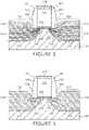
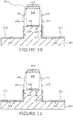
- Figure 1illustrates a cross-sectional view of a semiconductor device in accordance with one embodiment of the present invention.
- the semiconductor devicecomprises a substrate 200 made of a semiconductor material such as, but not limited to, monocrystalline silicon.
- the substrate 200is the silicon film of a silicon on insulator (SOI) substrate, or a multi-layered substrate comprising silicon, silicon germanium, germanium, III-V compound semiconductors.
- SOIsilicon on insulator
- a gate dielectric 310is formed over a channel region of the substrate 200.
- the dielectric layer 310is made from any well known insulative material, such as but not limited to silicon oxide (e.g., SiO 2 ).
- the dielectric layer 310is made of a high-k dielectric material having a substantially higher dielectric constant than silicon dioxide (i.e. k > 3.9). Examples of high-k dielectric materials include but are not limited to tantalum oxide (Ta 2 O 5 ), titanium oxide (TiO 2 ) and hafnium oxide (HfO 2 ).
- a gate electrode 320is formed over the gate dielectric 310.
- the gate electrode 320is made of any well known materials, such as but not limited to polysilicon.
- the gate electrode 320is made of a metal or metal alloy material such as, but not limited to, platinum, tungsten or titanium.
- a hard mask 410is formed on top of the gate electrode 320.
- hard mask 410is made of a material such as but not limited to silicon nitride or silicon oxynitride.
- Spacers 420, 440are formed on opposite sidewalls of the gate electrode 320. In one embodiment, spacers 420, 440 are formed along the entire sidewall width of the gate electrode 320. Spacers 420, 440 comprise sidewalls 421, 441, and bottom surfaces 422, 442. In one embodiment, the spacers 420, 440 are made of a material such as but not limited to a silicon nitride, silicon dioxide or silicon oxynitride.
- a recessed source interface 220 and a recessed drain interface 230are formed on the substrate 200 at opposite sides of the gate electrode 320.
- a portion of the recessed source interface 220extends laterally beneath the bottom surface 422 of the spacer 420 and beneath a portion of the gate electrode 320.
- a portion of the recessed drain interface 230extends laterally beneath the bottom surface 442 of the spacer 440 and beneath a portion of the gate electrode 320.
- a source region 501is formed over the recessed source interface 220.
- the source region 501comprises an epitaxial region 531 formed over the recessed source interface 220.
- a cap layer 541is formed over the epitaxial region 531.
- the source region 501comprises a source epi-tip region 503 that includes portions of the epitaxial region 531 and cap layer 541 formed directly beneath the spacer 420 and gate dielectric 310.
- a drain region 502is formed over the recessed drain interface 230.
- the drain region 502comprises an epitaxial region 532 formed over the recessed drain interface 230.
- a cap layer 542is formed over the epitaxial region 532.
- the drain region 502comprises a drain epi-tip region 504 that includes portions of the epitaxial region 532 and cap layer 542 formed directly beneath the spacer 440 and gate dielectric 310.
- the epitaxial regions 531, 532comprise silicon and carbon doped with phosphorus.
- the semiconductor device shown in Figure 1is a NMOS planar or trigate transistor with a Self-aligned Epi Tip (SET) architecture.
- the epitaxial regions 531, 532comprise silicon having a carbon concentration of about 0.5 atomic % to 4 atomic % and a phosphorus concentration of about 9E19 cm -3 to 3E21 cm -3 .
- the epitaxial regions 531, 532comprise silicon having a carbon concentration of 2.2 atomic % and a phosphorus concentration of 2E20 cm -3 .
- substitutional carbon(over 2 atomic %) in the epitaxial regions 531, 532 of the source and drain regions 501, 502 impart hydrostatic stress on the channel region, which enhances electron mobility. Furthermore, the substitutional carbon suppresses any phosphorus diffusion during any subsequent thermal anneals, thus reducing short channel effects.
- the cap layers 541, 542are phosphorous doped silicon cap layers having a phosphorus concentration of about 8E19 cm -3 to 3E21 cm -3 .
- the cap layers 541, 542are made of silicon having a phosphorus concentration of 2E21 cm -3 .
- the high phosphorus concentration level in the cap layers 541, 542reduces parasitic resistance, particularly in contact resistance between salicide and source/drain regions 501, 502.
- Figure 2illustrates a cross-sectional view of a semiconductor device similar to Figure 1 .
- the substrate 200is made of ⁇ 001 ⁇ silicon, and comprises a recessed source interface 240 having a ⁇ 111 ⁇ facet 241 in the ⁇ 111 ⁇ crystallographic plane of the ⁇ 001 ⁇ silicon substrate 200, and a recessed drain interface 250 having a ⁇ 111 ⁇ facet 251 in the ⁇ 111 ⁇ crystallographic plane of the ⁇ 001 ⁇ silicon substrate 200.
- the ⁇ 111 ⁇ facets 241, 251provide reduced volume in depletion and corresponding improved control of short channel effects.
- the recessed source and drain interfaces 240, 250each further comprises a ⁇ 010 ⁇ facet 242, 252 in the ⁇ 010 ⁇ crystallographic plane of the ⁇ 001 ⁇ silicon substrate 200, where the ⁇ 010 ⁇ facets 242, 252 extend directly beneath the gate electrode 320.
- the ⁇ 010 ⁇ facets 242, 252contribute to more precisely defining the metallurgical channel length of the semiconductor device and reduce short channel effects.
- the semiconductor device shown in Figure 2comprises a source region 501 and a drain region 502, each having an epitaxial region 531, 532 and a cap layer 541, 542.
- Epitaxial regions 531, 532 and cap layers 541, 542are formed over the recessed source and drain interfaces 240, 250 including their ⁇ 111 ⁇ facets 241, 251 and ⁇ 010 ⁇ facets 242, 252.
- the source region 501comprises a source epi-tip region 505 that includes portions of the epitaxial region 531 and cap layer 541 surrounded by the spacer 420, the gate dielectric 310 and the ⁇ 111 ⁇ , ⁇ 010 ⁇ facets 241, 242.
- the drain region 502comprises a drain epi-tip region 506 that includes portions of the epitaxial region 532 and cap layer 541 surrounded by the spacer 440, the gate dielectric 310 and the ⁇ 111 ⁇ , ⁇ 010 ⁇ facets 251, 252. Forming the source and drain epi-tip regions 505, 506 in relatively close proximity to the channel region induces a larger hydrostatic stress on the channel region, thus increasing electron mobility which results in higher drive current.
- Figure 3illustrates a cross-sectional view of a semiconductor device similar to Figure 2 .
- the source and drain regions 501, 502each comprises an epitaxial layer 610, 620 formed over the recessed source and drain interfaces 240, 250 including their ⁇ 111 ⁇ facets 241, 251 and ⁇ 010 ⁇ facets 242, 252.
- the source region 501comprises a source epi-tip region 611 that includes portions of the epitaxial layer 610 surrounded by the spacer 420, the gate dielectric 310 and the ⁇ 111 ⁇ , ⁇ 010 ⁇ facets 241, 242.
- the drain regioncomprises a drain epi-tip region 621 that includes portions of the epitaxial layer 610 surrounded by the spacer 440, the gate dielectric 310 and the ⁇ 111 ⁇ , ⁇ 010 ⁇ facets 251, 252. Forming the source and drain epi-tip regions 611, 621 in relatively close proximity to the channel region induces a larger hydrostatic stress on the channel region, thus increasing electron mobility which results in higher drive current.
- the epitaxial layer 610, 620comprises silicon doped with phosphorus.
- the epitaxial layers 610, 620comprise silicon having a phosphorus concentration of about 8E19 cm -3 to 3E21 cm -3 .
- the epitaxial layers 610, 620comprise silicon having a phosphorus concentration of 2E21 cm -3 .
- the high phosphorus concentration level in the epitaxial layers 610, 620reduces parasitic resistance, particularly in contact resistance between salicide and source/drain regions 501, 502.
- Figures 1 , 2 and 3illustrate the application of epitaxial regions in planar transistors to enhance electron mobility at the channel region or to reduce contact resistance at the source/drain regions. It can be appreciated that the epitaxial regions are not limited to planar transistors but can be fabricated on other devices, such as but not limited to a trigate transistor.
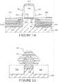
- Figure 4illustrates a perspective view of a tri-gate device comprising a substrate 200 having a semiconductor body or fin 260 (represented by dashed lines).
- a gate electrode 340is formed over 3 surfaces of the fin 260 to form 3 gates.
- a hard mask 410is formed on top of the gate electrode 340.
- Gate spacers 460, 470are formed at opposite sidewalls of the gate electrode 340.
- the source regioncomprises the epitaxial region 531 formed on a recessed source interface 266 and on a fin 260 sidewall.
- the cap layer 541is deposited over the epitaxial region 531.
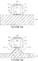
- FIGs 5A - 5Fillustrate a method of forming the semiconductor device as discussed in relation to Figure 1 .
- the fabrication of the semiconductor devicebegins by providing the substrate 200 as shown in Figure 5A .
- the gate dielectric 310is formed over a desired channel region of the substrate 200.
- the gate dielectric 310is formed by any well known methods, such as but not limited to physical vapor deposition (PVD), chemical vapor deposition (CVD) or atomic layer deposition (ALD).
- the gate electrode 320is formed over the gate dielectric 310.
- the gate electrode 320is a sacrificial gate electrode that is subsequently replaced by an actual gate electrode in a replacement gate process.
- the hard mask 410is formed on top of the gate electrode 320.
- the gate electrode 320 and hard mask 410are deposited using PVD or CVD, and then patterned using well known photolithography and etching techniques.
- Spacers 420, 440are then formed on opposite sidewalls of the gate electrode 320.
- Spacers 420, 440comprises sidewalls 421, 441, and bottom surfaces 422, 442 that are formed on the top surface of the substrate 200.
- the spacers 420, 440are formed by using well known techniques, such as depositing a layer of spacer material over the entire substrate 200 including the gate electrode 320, and then anisotropically etching the layer of spacer material to form the spacers 420, 440 on the sidewalls of gate electrode 320.
- a source region and a drain regionare formed on the substrate 200. Fabrication of the source and drain regions begins by recessing portions of the substrate 200 using well known etching techniques, such as but not limited to dry etching or wet etching. A wet etching comprising an etchant chemistry that is substantially selective to the substrate 200 is utilized to recess the substrate 200 so as to form a recessed source interface 220 and a recessed drain interface 230 as shown in Figure 5B .
- the wet etchingundercuts the spacers 420, 440 and forms a source epi-tip cavity 271 between the bottom surface 422 of spacer 420 and the recessed source interface 220, and forms a drain epi-tip cavity 272 between the bottom surface of spacer 440 and the recessed drain interface 230.
- the source epi-tip cavity 271 and drain epi-tip cavity 272expose the bottom surfaces 422, 442 of the spacers 420, 440.
- the source epi-tip cavity 271 and drain epi-tip cavity 272also expose portions of the gate dielectric 310.
- a portion of the recessed source interface 220extends laterally beneath the spacer 420 and beneath a portion of the gate electrode 320.
- a portion of the recessed drain interface 230extends laterally beneath the spacer 440 and beneath a portion of the gate electrode 320.
- the wet etchingcan be controlled (e.g. by adjusting the etching duration) so that the source and drain epi-tip cavities 271, 272 do not expose the gate dielectric 310.
- the recessed source interface 220only extends laterally beneath the spacer 420, and the recessed drain interface 230 only extends laterally beneath the spacer 440.
- the recessed source and drain interfaces 220, 230define the channel region of the semiconductor device.
- the channel regionrefers to the portion of the substrate 200 located directly beneath the gate dielectric 310 and between the recessed source and drain interfaces 220, 230.
- an epitaxial regionis deposited over each of the recessed source and drain interfaces 220, 230 by alternatingly exposing the substrate 200 to a first precursor and a second precursor. Fabrication of the epitaxial region begins, in Figure 5C , by exposing the entire substrate 200 to the first precursor so as to deposit epitaxial films 511, 512 on the recessed source and drain interfaces 220, 230.
- the substrate 200is made of monocrystalline silicon
- the recessed source and drain interfaces 220, 230are monocrystalline surfaces that allow epitaxial growth of the epitaxial films 511, 512 thereon.
- the hard mask 410, the spacers 420, 440, and the gate dielectric 310are non-crystalline surfaces.
- an amorphous layer 513is deposited on the top surface of the hard mask 410, on the sidewalls 421, 441 and bottom surfaces 422, 442 of the spacers 420, 440, and on portions of the bottom surface of the gate dielectric 310.
- the first precursorcomprises a silicon-containing compound, a carbon-containing compound, and a dopant.
- the silicon-containing compoundincludes, but not limited to, silanes and halogenated silanes.
- Such silicon-containing compoundincludes silane (SiH 4 ), disilane (Si 2 H 6 ), trisilane (Si 3 H 8 ), dichlorosilane (SiH 2 Cl 2 ), and penta-chloro silane.
- the carbon-containing compoundincludes, but not limited to, organosilanes.
- the carbon-containing compoundcomprises mono-methyl silane (CH 3 -SiH 3 ).
- the carbon-containing compoundis mixed with hydrogen (H 2 ) or argon.
- mono-methyl silane (CH 3 -SiH 3 )is mixed with hydrogen (H 2 ) or argon with the CH 3 -SiH 3 concentration in the range of 0.5% to 20%.
- the dopantis a n-type dopant such as, but not limited to, phosphorus or arsenic.
- the Phosphorus dopantis incorporated in the epitaxial film using phosphine (PH 3 ) without any dilution in Hydrogen or an inert gas, such as N 2 or Ar.
- the phosphine gasis mixed with hydrogen, for example as a mixture of 3% phosphine (PH 3 ) in hydrogen (H 2 ).
- the first precursoris delivered or released onto the substrate 200 with a carrier gas.
- the carrier gasincludes, but is not limited, to hydrogen (H 2 ), or any inert gas such as nitrogen (N 2 ) argon and helium and any combinations thereof.
- the substrate 200is exposed to the first precursor at a temperature of about 500 to 700 degrees Celsius, at a pressure of about 5 to 300 torr, and for a time duration of about 3 to 60 seconds.
- the substrate 200is exposed to the first precursor at a temperature of 600 degrees Celsius, at a pressure of 30 torr, and for a time duration of 15 seconds.
- the epitaxial films 511, 512are grown to have a thickness of about 6 to 100 Angstroms. In a specific example, the epitaxial films 511, 512 are grown to have a thickness of 50 Angstroms.
- the deposited epitaxial films 511, 512are crystalline films containing silicon and carbon doped with phosphorus (i.e. in-situ carbon and phosphorus doped silicon layer).
- the amorphous layer 513contains silicon and carbon doped with phosphorus.
- An optional surface pre-treatmentcan be performed on the substrate 200 before exposing it to the first precursor to facilitate epitaxial growth and reduce surface defects.
- the surface pre-treatmentincludes a hydrogen bake treatment performed on the substrate 200 (in Figure 5B ) to clean the recessed source and drain interfaces 220, 230.
- the hydrogen bake treatmentdesorbs oxygen and renders surface reconstruction so that the epitaxial films 511, 512 can readily nucleate without formation of defects.
- the hydrogen bake treatmentis performed at around 700 to 1050 degrees Celsius for a duration of about 10 to 120 seconds.
- hydrogen chloride (HCl)is added to the hydrogen bake treatment.
- the hydrogen chloride (HCl)enables removal of about 1 to 3 monolayers of the recessed source and drain interfaces 220, 230 so that they are free of oxygen, hydrocarbons and any other contaminants.
- the hydrogen bake treatment with hydrogen chloride (HCl)is performed at a lower temperature of around 700 to 900 degrees Celsius for a duration of about 10 to 120 seconds.
- chlorine (Cl 2 ), germane (GeH 4 ) or phosphine (PH 3 )can be used as an additional or alternative chemical compound for hydrogen chloride (HCl).
- the surface pre-treatmentutilizes an etch step to clean the recessed source and drain interfaces 220, 230.
- the etch stepuses an etchant gas, such as but not limited to hydrogen (H 2 ), anhydrous hydrochloric acid (HCl), or a mixture of germane (GeH 4 ) and hydrogen (H 2 ).
- the surface pre-treatmentuses a combination of the etch step and the hydrogen bake treatment.
- a purging processcan be performed to remove the first precursor and other by-products from the substrate 200.
- the purging processinjects an inert gas, such as but not limited to nitrogen (N 2 ), helium or argon to remove any unreacted first precursor or by-products.
- the entire substrate 200is exposed to the second precursor to remove the amorphous layer 513 from the sidewalls 421, 441 and bottom surfaces 422, 442 of the spacers 420 , 440. Furthermore, the second precursor also removes any amorphous layer 513 formed on the hard mask 410 and beneath the gate dielectric 310.
- the second precursor 900uses an etchant chemistry that etches the amorphous layer 513 faster than the epitaxial films 511, 512.
- the second precursor 900is an etchant gas, such as but not limited to hydrogen (H 2 ), anhydrous hydrochloric acid (HCI), and a mixture of germane (GeH 4 ) and hydrogen (H 2 ). Germane (GeH 4 ) enables etch through catalysis, thus providing high etch rate at low temperatures.
- the substrate 200is exposed to the second precursor at a pressure of about 30 to 300 torr, and for a time duration of about 5 to 60 seconds. In a specific embodiment, the substrate 200 is exposed to the second precursor at a pressure of 80 torr, and for a time duration of 20 seconds. In one example, the temperature is maintained at substantially the same level when exposing the substrate 200 to both the first precursor and the second precursor.
- the second precursorDue to the weak chemical bonding between the amorphous layer 513 and the hard mask 410, spacers 420, 440 and gate dielectric 310, the second precursor easily removes the amorphous layer 513 deposited thereon. The second precursor reacts with the amorphous layer 513 to convert it into by-products, thus removing the amorphous layer 513 from the hard mask 410, spacers 420, 440 and gate dielectric 310.
- the epitaxial films 511, 512have strong chemical bonds with the recessed source and drain interfaces 220, 230. Due to the strong chemical bonds, only small portions of the epitaxial films 511, 512 are removed by the second precursor.
- the thickness of the epitaxial films 511, 512 deposited during Figure 5C or the duration of exposing the second precursor to the substrate 200 in Figure 5Dcan be adjusted so as to effectively remove the amorphous layer 513 while maintaining sufficient thickness for the epitaxial films 511, 512.
- Figures 5C and 5Dillustrate one deposition-etch cycle of forming the epitaxial films 511, 512 over the recessed source and drain interfaces 220, 230.
- the deposition-etch cycleis repeated using the same type of first and second precursors until a desired number of epitaxial films are deposited.
- Figure 5Eshows epitaxial regions 531, 532 containing ten epitaxial films each.
- the epitaxial regions 531, 532are not limited to only ten layers of epitaxial films each. In one example, about 3 to 100 deposition-etch cycles are performed to form the epitaxial regions 531, 532. In a specific example, 30 deposition-etch cycles are performed to form the epitaxial regions 531, 532 having a thickness of around 30 nanometers.
- the epitaxial regions 531, 532are deposited with a graded concentration of carbon or phosphorus.
- the carbon and phosphorus concentration of each epitaxial film depositioncan be optimized to provide optimal selectivity and defect-free epitaxy.
- the graded carbon or phosphorus concentrationpromotes the removal of the amorphous material during the deposition-etch cycles.
- the graded carbon concentration of the epitaxial regions 531, 532(shown in Figure 5E ) begins at around 0.5 atomic % for the lowest epitaxial film and is gradually increased to a desired level of about 2 atomic % in the uppermost epitaxial film.
- the graded phosphorus concentration level of the epitaxial regions 531, 532begins at around 8E19 cm -3 for the lowest epitaxial film and is gradually increased to a desired level of around 2E21 cm -3 in the uppermost epitaxial film.
- the epitaxial regions 531, 532are deposited with a combination of graded carbon concentration (0.5 - 2 atomic %) and graded phosphorus concentration (8E19 - 2E21 cm -3 ).
- the epitaxial regions 531, 532are selectively formed over the recessed source and drain interfaces 220, 230 as shown in Figure 5E .
- the removal of the amorphous layer 513 during each deposition-etch cycleresults in voids or cavities 281,282 formed between the bottom surfaces 422, 442 of spacers 420, 440 and the top surfaces of the epitaxial regions 531, 532.
- the cavities 281, 282also extend between portions of the gate dielectric 310 and the epitaxial regions 531, 532.
- the cavities 281, 282may cause detrimental effects on the transistor performance, and thus need to be eliminated.
- the cavities 281, 282are substantially backfilled by cap layers 541, 542 selectively deposited over the epitaxial regions 531, 532 as shown in Figure 5F .
- the cap layers 541, 542are selectively deposited over the epitaxial regions 531, 532 in a single deposition process by exposing the substrate 200 to a third precursor.
- the third precursorcomprises the same silicon-containing compound and dopant of the first precursor, and the same etchant gas of the second precursor.
- the third precursoruses the same phosphorus dopant to form cap layers 541, 542.
- the crystalline surfaces of the epitaxial layers 531, 532allow epitaxial growth of cap layers 541, 542 thereon, and as a result, the cap layers 541, 542 are epitaxial layers containing silicon doped with phosphorus.
- the phosphorus doped silicon cap layers 541, 542provides an advantage of inducing tensile stress on the channel region, thereby increasing electron mobility and improving the device performance.
- a co-flown deposition techniqueis used to expose the substrate 200 to the silicon-containing compound, the dopant, and the etchant gas at the same time.
- the etchant gasdoes not include germane (GeH 4 ).
- the etchant gaseasily removes any silicon and phosphorus-containing compound that are weakly bonded on the hard mask 410 and spacers 420, 440 so that the cap layers 541, 542 are deposited over the epitaxial regions 531, 532 and not deposited on the hard mask 410 or the spacers 420, 440.
- the substrate 200is exposed to the third precursor at a temperature of about 550 to 800 degrees Celsius, at a pressure of about 10 torr to atmospheric pressure, and for a time duration of about 30 to 900 seconds.
- the substrate 200is exposed to the first precursor at a temperature of 635 degrees Celsius, at a pressure of 600 torr, and for a time duration of 180 seconds.
- the cap layers 541, 542are grown to have a thickness of about 50 to 500 Angstroms. In a specific embodiment, the cap layers 541, 542 are grown to have a thickness of 300 Angstroms.
- Source epi-tip region 531 and cap layer 541 directly beneath the spacer 420 and gate dielectric 310forms the source epi-tip region 503.
- portions of the epitaxial region 532 and cap layer 542 directly beneath the spacer 440 and gate dielectric 310forms the drain epi-tip region 504.
- the stresscan be further amplified by increasing the carbon concentrations of the source and drain epi-tip regions 503, 504 during fabrication of the epitaxial regions 531, 532.
- the carbon concentrations of the source and drain epi-tip regions 503,504also help to suppress any phosphorus diffusion during subsequent thermal anneals.
- the gate electrode 320is a sacrificial gate electrode that is subsequently replaced by an actual gate electrode in a replacement gate process.
- the replacement gate processbegins by depositing a mask on the cap layers 541, 542 and then planarizing the mask to be coplanar with the hard mask 410 (not shown). Next, the hard mask 410 and gate electrode 320 are removed using well known etching techniques. After removing the hard mask 410 and gate electrode 320, the actual gate electrode is then deposited on the gate dielectric 310.
- the actual gate electrodeis a metal gate electrode comprising materials such as, but not limited to, platinum, tungsten or titanium. This completes the fabrication of the semiconductor device shown in Figure 1 .
- Figures 6A - 6Fillustrate a method of forming the semiconductor device as discussed in relation to Figure 2 .
- the fabrication of the semiconductor devicebegins by providing the substrate 200 as shown in Figure 6A .
- the semiconductor device shown in Figure 6Ais the same as Figure 5A , and thus will not be discussed in detail.
- the semiconductor devicecomprises the gate dielectric 310 formed over a desired channel region of the substrate 200.
- the gate electrode 320is formed over the gate dielectric 310.
- the gate electrode 320is a sacrificial gate electrode that is subsequently replaced by an actual gate electrode in a replacement gate process.
- Hard mask 410is formed on top of the gate electrode and spacers 420, 440 are formed at the sidewalls of the gate electrode 320.
- a source region and a drain regionare formed on the substrate 200.
- fabrication of the source and drain regionsbegins by recessing portions of the substrate 200 using well known etching techniques, such as but not limited to dry etching or wet etching.
- a wet etchingthat is substantially selective to the substrate 200 is utilized to recess the substrate 200 so as to form a recessed source interface 240 and a recessed drain interface 250 as shown in Figure 6B .
- the substrate 200is made of ⁇ 001 ⁇ silicon.
- the wet etchuses an etchant chemistry that etches the ⁇ 001 ⁇ silicon substrate 200 based on crystallographic direction, and in particular etches the ⁇ 001 ⁇ silicon substrate 200 much more slowly along its ⁇ 111 ⁇ crystallographic plane to form the ⁇ 111 ⁇ facets 241, 251 as the etch proceeds much more rapidly in other crystallographic directions.
- a source epi-tip cavity 271is formed between the bottom surface 422 of spacer 420 and the ⁇ 111 ⁇ facet 241.
- a drain epi-tip cavity 272is formed between the bottom surface of spacer 440 and the ⁇ 111 ⁇ facet 251.
- the wet etch chemistryincludes, but not limited to, an ammonia-based or amine-based etchant.
- ammonia-based etchantsare ammonium hydroxide (NH4OH), tetramethylammonium hydroxide (TMAH) and benzyltrimethylammonium hydroxide (BTMH).
- TMAHtetramethylammonium hydroxide
- BTMHbenzyltrimethylammonium hydroxide
- the wet etch chemistryincludes other types of etchants, such as potassium hydroxide (KOH) and sodium hydroxide (NaOH).
- the wet etchfurther creates ⁇ 010 ⁇ facets 242, 252 in the channel region of the ⁇ 001 ⁇ silicon substrate 200.
- the ⁇ 010 ⁇ facets 242, 252extends directly beneath the gate dielectric 310.
- ⁇ 010 ⁇ facets 242, 252are formed up to a length of around 3 nanometers from the gate dielectric 310.
- an epitaxial regionis deposited over each of the recessed source and drain interfaces 240, 250 by alternatingly exposing the substrate 200 to a first precursor and a second precursor.
- the method of fabricating the epitaxial regionis similar to the methods of fabrication discussed in Figures 5C, 5D and 5E .
- an optional surface pre-treatmentcan be performed on the substrate 200 to facilitate epitaxial growth and reduce surface defects.
- the surface pre-treatmentcomprises a hydrogen bake treatment and/or etching step as previously discussed in Figure 5C to clean the recessed source and drain interfaces 240, 250.
- the entire substrate 200is exposed to the first precursor so at to deposit epitaxial films 511, 512 on the recessed source and drain interfaces 240, 250.
- the recessed source and drain interfaces 240, 250including their ⁇ 111 ⁇ facets 241, 251 and ⁇ 010 ⁇ facets 242, 252, are monocrystalline surfaces that allow epitaxial growth of the epitaxial films 511, 512 thereon.
- the hard mask 410, the spacers 420, 440, and the gate dielectric 310are non-crystalline surfaces, and thus the amorphous layer 513 is deposited thereon.
- the same first precursor and process conditions, as discussed in relation to Figure 5Care applicable here and will not be discussed.
- the entire substrate 200is similarly exposed to the second precursor to remove the amorphous layer 513 from the sidewalls 421, 441 and bottom surfaces 422, 442 of the spacers 420 , 440. Furthermore, the second precursor also removes any amorphous layer 513 formed on the hard mask 410 and beneath the gate dielectric 310.
- the same second precursor and process conditions, as discussed in relation to Figure 5Dare applicable here and will not be discussed.
- Figures 6C and 6Dillustrate one deposition-etch cycle of forming the epitaxial films 511, 512 over the recessed source and drain interfaces 240, 250 including their ⁇ 111 ⁇ facets 241, 251 and ⁇ 010 ⁇ facets 242, 252.
- the deposition-etch cycleis repeated until a desired number of epitaxial films are deposited.
- Figure 6Eshows epitaxial regions 531, 532 containing ten epitaxial films each.
- the epitaxial regions 531, 532are deposited with a graded concentration of carbon or phosphorus as previously described in Figure 5E .
- the epitaxial regions 531, 532are deposited with a graded carbon concentration of around 0.5 atomic % for the lowest epitaxial film and are gradually increased to a desired level of about 2 atomic % for the uppermost epitaxial film.
- the epitaxial regions 531, 532are deposited with a graded phosphorus concentration level of around 8E19 cm -3 for the lowest epitaxial film and are gradually increased to a desired level of around 2E21 cm -3 for the uppermost epitaxial film.
- the epitaxial regions 531, 532are deposited with a combination of graded carbon concentration (0.5 - 2 atomic %) and graded phosphorus concentration (8E19 - 2E21 cm -3 ).
- the removal of the amorphous layer 513 during each deposition-etch cyclesimilarly results in cavities 281,282 formed between the bottom surfaces 422, 442 of spacers 420, 440 and the top surfaces of the epitaxial regions 531, 532.
- the cavities 281, 282are substantially backfilled by the cap layers 541, 542 selectively deposited over the epitaxial regions 531, 532 as shown in Figure 6F .
- the cap layers 541, 542are selectively deposited over the epitaxial regions 531, 532 in a single deposition process by exposing the substrate 200 to a third precursor.
- the third precursoruses the same phosphorus dopant to form cap layers 541, 542.
- the crystalline surfaces of the epitaxial regions 531, 532allow epitaxial growth of cap layers 541, 542 thereon, and as a result, the cap layers 541, 542 are epitaxial layers containing silicon doped with phosphorus. This completes the fabrication of the semiconductor device shown in Figure 2 .
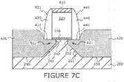
- Figures 7A - 7Cillustrate a method of forming the semiconductor device as discussed in relation to Figure 3 .
- the fabrication of the semiconductor devicebegins by providing the substrate 200.
- the semiconductor device shown in Figure 7Ais the same as Figure 5A , and thus will not be discussed here.
- a source region and a drain regionare formed on the substrate 200.
- fabrication of the source and drain regionsbegins by recessing portions of the substrate 200 using well known etching techniques, such as but not limited to dry etching or wet etching.
- the wet etching used in Figure 6Bis similarly applied here to recess the substrate 200 so as to form a recessed source interface 240 and a recessed drain interface 250, as shown in Figure 7B .
- the wet etchuses the same etchant chemistry as described in relation to Figure 6B to form ⁇ 111 ⁇ facets 241, 251 in the ⁇ 111 ⁇ crystallographic plane of the ⁇ 001 ⁇ silicon substrate 200.
- the wet etchfurther creates ⁇ 010 ⁇ facets 242, 252 in the channel region of the ⁇ 001 ⁇ silicon substrate 200.
- epitaxial layers 610, 620are selectively deposited over the recessed source and drain interfaces 240, 250 as shown in Figure 7C .
- the epitaxial layers 610, 620are selectively deposited in a single deposition process by exposing the substrate 200 to a precursor comprising an etchant gas.
- the precursorcomprises the silicon-containing compound and dopant similarly described in Figure 5C .
- the silicon-containing compoundincludes, but not limited to, silanes and halogenated silanes.
- Such silicon-containing compoundincludes silane (SiH 4 ), disilane (Si 2 H 6 ), trisilane (Si 3 H 8 ), dichlorosilane (SiH 2 Cl 2 ), and penta-chloro silane.
- the dopantis a n-type dopant such as, but not limited to, phosphorus or arsenic.
- the phosphorus dopantis introduced into the epitaxial layers using phosphine (PH 3 ) without any dilution in Hydrogen or an inert gas, such as N 2 or Ar.
- the phosphine gasis mixed with hydrogen, for example as a mixture of 3% phosphine (PH 3 ) in hydrogen (H 2 ).
- the etchant gas of the precursorincludes, but is not limited to hydrogen (H 2 ) and anhydrous hydrochloric acid (HCI).
- a co-flown deposition techniqueis used to deliver the precursor, including the etchant gas to the substrate 200 at the same time.
- the substrate 200is exposed to the precursor at a temperature of about 550 to 800 degrees Celsius, at a pressure of about 10 torr to atmospheric pressure, and for a time duration of about 30 to 2000 seconds.
- the substrate 200is exposed to the first precursor at a temperature of 635 degrees Celsius, at a pressure of 600 torr, and for a time duration of 800 seconds.
- the epitaxial layers 610, 620are grown to have a thickness of about 30 to 2000 Angstroms. In a specific example, the epitaxial layers 610, 620 are grown to have a thickness of 750 Angstroms. In the case where a phosphorus dopant is used, the epitaxial layers 610, 620 comprise silicon doped with phosphorus.
- the recessed source and drain interfaces 240, 250 including their ⁇ 111 ⁇ facets 241, 251 and ⁇ 010 ⁇ facets 242, 252are monocrystalline surfaces that allow epitaxial growth of the epitaxial layers 610, 620 thereon. Since the hard mask 410 and spacers 420, 440 have non-crystalline surfaces, the etchant gas easily removes any silicon and phosphorus-containing compound that are weakly bonded on the hard mask 410 and spacers 420, 440 during deposition so that the epitaxial layers 610, 620 are deposited over the recessed source and drain interfaces 240, 250 and not deposited on the hard mask 410 or spacers 420, 440.
- the source and drain epi-tip regions 611, 621in relatively close proximity to the channel region, a larger hydrostatic stress is induced on the channel region, resulting in higher electron mobility.
- the phosphorus doped silicon epitaxial layers 610, 620induces tensile stress on the channel region, thereby increasing electron mobility and improving the device performance. This completes the fabrication of the semiconductor device shown in Figure 3 .
- an optional surface pre-treatmentcan be performed on the substrate 200 before exposing it to the precursor to facilitate epitaxial growth and reduce surface defects.
- a similar hydrogen bake treatment described in relation to Figure 5Cis performed on the substrate 200 (in Figure 7B ) to clean the recessed source and drain interfaces 240, 250 including theirs ⁇ 111 ⁇ facets 241, 251 and ⁇ 010 ⁇ facets 242, 252.
- Figures 8A - 8Iillustrate a method of forming the tri-gate device as discussed in relation to Figure 4 .
- the fabrication of the tri-gate devicebegins by providing the substrate 200 as shown in Figure 8A .
- the substrate 200comprises a semiconductor body or fin 260 extending from the substrate 200 through the isolation regions 710, 720.
- the isolation regions 710, 720are shallow trench isolation (STI) regions formed by common techniques, such as etching the substrate 200 to form trenches, and then depositing oxide material onto the trenches to form the STI regions.
- the isolation regions 710, 720are made from any well known insulative material, such as but not limited to silicon oxide (e.g., SiO 2 ).
- the fin 260comprises a top surface 261 above the isolation regions 700.
- the fin 260further includes a front surface 262 exposed above the isolation region 710, and a back surface 263 exposed above the isolation region 720.
- the fin 260is made from the same semiconductor materials as the substrate 200.
- a gate dielectric 330is formed over a portion of the top surface 261, the front surface 262 and the back surface 263.
- the gate dielectric 330is formed by any well known methods, such as but not limited to physical vapor deposition (PVD), chemical vapor deposition (CVD) or atomic layer deposition (ALD).
- a gate electrode 340is formed over the gate dielectric 330, and exposing portions 264, 265 of the fin 260 at either sides of the gate electrode 340.
- the gate electrode 340is made of any well known materials, such as but not limited to polysilicon.
- the gate electrode 340 formed over the top surface 261, the front surface 262 and the back surface 263creates three gates for the tri-gate device.
- the hard mask 410is then formed on top of the gate electrode 320.
- gate spacers 460, 470are deposited on opposite sidewalls of the gate electrode 340 as shown in Figure 8C .
- the spacers 460, 470are formed by using well known techniques, such as depositing a layer of spacer material over the entire substrate 200 including the gate electrode 320, and then anisotropically etching the layer of spacer material to form the spacers 460, 470 on the sidewalls of gate electrode 340.
- fin spacers 480, 490are formed on the sidewalls of the exposed portions 264, 265 of the fin 260.
- the gate spacers 460, 470 and fin spacers 480, 490are made of a material such as but not limited to a silicon nitride, silicon dioxide or silicon oxynitride.
- a source region and a drain regionare formed on the substrate 200.
- fabrication of the source and drain regionsbegins in Figure 8D by removing the fin spacers 480, 490 from the sidewalls of the exposed portions 264, 265 of the fin 260.
- the fin spacers 480, 490are removed by well known etching techniques, such as but not limited to dry etching or wet etching.
- an anisotropic wet-etchis used to completely remove the fin spacers 480, 490 from the exposed portions 264, 265 of the fin 260.
- the anisotropic wet-etchalso removes portions of the gate spacers 460, 470, thus exposing portions of the hard mask 410 sidewalls. Since the gate spacers 460, 470 have a larger height and thickness than the fin spacers 480, 490, the anisotropic wet-etch removes the fin spacers 480, 490 faster than the gate spacers 460, 470.
- the anisotropic wet-etchcan be controlled to completely remove the fin spacers 480, 490 but leaving sufficient thickness of the gate spacers 460, 470 on the gate electrode 340 so that the gate electrode 340 sidewalls are not exposed.
- an etchingis performed on the substrate 200 to recess the exposed portions 264, 265 of the fin 260.
- the etchinguses an etchant chemistry that is substantially selective to the fin 260 to recess the exposed portion 264 so as to form a recessed source interface 266 below the top surface of the isolation regions 710, 720, and to form a fin sidewall 267 as shown in Figure 8E .
- the exposed portion 264is recessed to form a recessed drain interface 268 and a fin sidewall 269.
- the recessed source and drain interfaces 266, 268are about 100 to 400 Angstroms below the top surface of the isolation regions 710, 720.
- Figure 9illustrates a cross-sectional view of the tri-gate device showing the fin sidewall 267 extending from the top surface 261 to the recessed source interface 266, and the fin sidewall 269 extending from the top surface 261 to the recessed drain interface 268.
- the fin sidewalls 267, 269are substantially coplanar or flushed with the gate spacers 460, 470 sidewalls 461, 471.
- the fin sidewalls 267, 269are ⁇ 110 ⁇ facets in the ⁇ 110 ⁇ crystallographic plane of the substrate 200
- the recessed source and drain interfaces 266, 268are ⁇ 100 ⁇ facets in the ⁇ 100 ⁇ crystallographic plane of the substrate 200.
- an isotropic etchis used to form fin sidewalls 267, 269 recessed within the gate spacers 460, 470.
- Figure 8E'is a perspective view of the trigate device showing the fin sidewall 267 recessed within the gate spacer 470.
- Figure 9'is a cross-sectional view showing both the fin sidewalls 267, 269 recessed beneath the gate spacer 460, 470.
- the fin sidewalls 267, 269are recessed until about 25 to 200 Angstroms from the gate spacer sidewalls 461, 471.
- an epitaxial regionis then deposited over each of the recessed source and drain interfaces 266, 268 by alternatingly exposing the substrate 200 to a first precursor and a second precursor.
- the method of fabricating the epitaxial regionas illustrated in Figures 8F, 8G and 8H , is similar to the methods of fabrication discussed in Figures 5C, 5D and 5E .
- the entire substrate 200is exposed to the first precursor so at to deposit an epitaxial film 511 on the recessed source interface 266 and fin sidewall 267.
- an epitaxial film 512is deposited on the recessed drain interface 268 and fin sidewall 269 as shown in cross-sectional view of Figure 10 .
- the recessed source and drain interfaces 266, 268, and the fin sidewalls 267, 269are monocrystalline surfaces that allow epitaxial growth of the epitaxial films 511, 512 thereon.
- the hard mask 410, the gate spacers 460, 470, and isolation regions 710, 720are non-crystalline surfaces, and thus the amorphous layer 513 is formed thereon.
- the same first precursor and process conditions, as discussed in relation to Figure 5Care applicable here and will not be discussed.
- FIG 8Gthe entire substrate 200 is similarly exposed to the second precursor to remove the amorphous layer 513 from the gate spacers 460, 470, and isolation regions 710, 720. Furthermore, the second precursor also removes any amorphous layer 513 formed on the hard mask 410.
- Figure 11shows a cross-sectional view of the tri-gate device after the amorphous layer 513 has been removed. The same second precursor and process conditions, as discussed in relation to Figure 5D , are applicable here and will not be discussed.
- Figures 8F-8G and Figures 10-11illustrate one deposition-etch cycle of forming the epitaxial films 511, 512 over the recessed source and drain interfaces 266, 268 and the fin sidewalls 267, 269.
- the deposition-etch cycleis repeated until a desired number of epitaxial films are deposited.
- the final epitaxial regions 531, 532comprise five epitaxial films as shown in Figure 12 .
- the epitaxial regions 531, 532are deposited with a graded concentration of carbon or phosphorus as previously described in Figure 5E .
- the epitaxial regions 531, 532are deposited with a graded carbon concentration of around 0.5 atomic % for the lowest epitaxial film and are gradually increased to a desired level of about 2 atomic % for the uppermost epitaxial film.
- the epitaxial regions 531, 532are deposited with a graded phosphorus concentration level of around 8E19 cm -3 for the lowest epitaxial film and are gradually increased to a desired level of around 2E21 cm -3 for the uppermost epitaxial film.
- the epitaxial regions 531, 532are deposited with a combination of graded carbon concentration (0.5 - 2 atomic %) and graded phosphorus concentration (8E19 - 2E21 cm -3 ).
- the epitaxial regions 531, 531are formed in closer proximity to the channel region of the tri-gate device, thus inducing a higher amount of stress on the channel region.
- the removal of the amorphous layer 513 during each deposition-etch cyclesimilarly results in voids or cavities 281,282 formed between the epitaxial regions 531, 532 and the isolation regions 710, 720 as shown in Figures 8H and 13 .
- the cavities 281, 282are substantially backfilled by the cap layers 541, 542 selectively deposited over the epitaxial regions 531, 532 as shown in Figures 81 , 14 and 15 .
- the cap layers 541, 542are selectively deposited over the epitaxial regions 531, 532 in a single deposition process by exposing the substrate 200 to a third precursor.
- the third precursoruses the same phosphorus dopant to form cap layers 541, 542.
- the crystalline surfaces of the epitaxial regions 531, 532allow epitaxial growth of cap layers 541, 542 thereon, and as a result, the cap layers 541, 542 are epitaxial layers containing silicon doped with phosphorus.
- the phosphorus doped silicon cap layers 541, 542provide an advantage of inducing tensile stress on the channel region of the semiconductor fin 260, which increases the electron mobility and improves the device performance. This completes the fabrication of the semiconductor device shown in Figure 4 .
Landscapes
- Engineering & Computer Science (AREA)
- Physics & Mathematics (AREA)
- Condensed Matter Physics & Semiconductors (AREA)
- General Physics & Mathematics (AREA)
- Manufacturing & Machinery (AREA)
- Computer Hardware Design (AREA)
- Microelectronics & Electronic Packaging (AREA)
- Power Engineering (AREA)
- Chemical & Material Sciences (AREA)
- Materials Engineering (AREA)
- Insulated Gate Type Field-Effect Transistor (AREA)
- Thin Film Transistor (AREA)
Description
- The present invention relates to a semiconductor device having doped epitaxial regions.
- Increasing the performance of semiconductor devices, in particular transistors, has always been a major consideration in the semiconductor industry. For example, during the design and fabrication of metal oxide semiconductor field effect transistors (MOSFETs), it has always been a common goal to increase the electron mobility of the channel region and to reduce the parasitic resistance to improve device performance.
- Other methods of improving device performance include, for example, reducing the overall resistance of the MOSFET by doping the region between the source/drain regions and the channel region, which is referred to as the 'tip' or source/drain extension regions of the MOSFET. For example, a dopant is implanted in the source/drain regions and an annealing step diffuses the dopant towards the channel region. However, there are limits to controlling the dopant concentration and location. Furthermore, the implant and diffusion method does not address the issues of lateral undercut or parasitic resistance at the tip regions.
US 2008/124878 A1 discloses a multi-component strain-inducing semiconductor region. In an embodiment, formation of such a strain-inducing semiconductor region laterally adjacent to a crystalline substrate results in a uniaxial strain imparted to the crystalline substrate, providing a strained crystalline substrate. In one embodiment, the multi-component strain-inducing material region comprises a first portion and a second portion which are separated by an interface. The concentration of charge-carrier dopant impurity atoms of the two portions are different from one another at the interface.US 2009/075029 A1 discloses a semiconductor substrate having recesses filled with heteroepitaxial silicon-containing material with different portions having different impurity concentrations. Strained layers can fill recessed source/drain regions in a graded, bottom-up fashion. Layers can also line recess sidewalls with one concentration of strain-inducing impurity and fill the remainder to the recess with a lower concentration of the impurity. In the latter case, the sidewall liner can be tapered.US 2008/242061 A1 discloses a precursor gas mixture for depositing an epitaxial carbon-doped silicon film. The precursor gas mixture is comprised of a volume of a silicon precursor gas, a volume of acetylene gas and a volume of a carrier gas. A method of forming a semiconductor structure having an epitaxial carbon-doped silicon film is also described. In the method, a substrate having a high polarity dielectric region and a low polarity crystalline region is provided. A precursor gas is flowed to provide a silyl surface above the high polarity dielectric region and a carbon-doped silicon layer above the low polarity crystalline region. The silyl surface is then removed from above the high polarity dielectric region. The flowing and removing steps are repeated to provide a carbon-doped silicon film of a desired thickness above the low polarity crystalline region.US 2008/0067557 A1 discloses a MOS device with strain-inducing source/drain regions, comprising non-conformal stressors. Stressors are disclosed as being germanium or carbon doped silicon, and may be doped with p-type or n-type impurities.US2008/0026531 A1 discloses a field effect transistor with multi-layered strain-inducing source/drain regions; the source/drain regions comprise carbon impurities.- The invention is defined by the subject matter of independent claim 1. Advantageous embodiments of the invention are subject to the dependent claims.
Figure 1 is a cross-sectional view that illustrates a semiconductor device in accordance with one embodiment of the present invention.Figure 2 is a cross-sectional view that illustrates a semiconductor device in accordance with another embodiment of the present invention.Figure 3 is a cross-sectional view that illustrates a semiconductor device in accordance with an example not forming part of the present invention.Figure 4 is a perspective view that illustrates a semiconductor device in accordance with an example not forming part of the present invention.Figures 5A - 5F are cross-sectional views that illustrate the method of fabricating the semiconductor device shown inFigure 1 .Figures 6A - 6F are cross-sectional views that illustrate the method of fabricating the semiconductor device shown inFigure 2 .Figures 7A - 7C are cross-sectional views that illustrate the method of fabricating the semiconductor device shown inFigure 3 .Figures 8A - 8I are perspective views that illustrate the method of fabricating the semiconductor device shown inFigure 4 .Figures 9 - 15 are cross-sectional views of the semiconductor device shown inFigures 8E - 81 .Figure 8E' is a perspective view that illustrates an alternative embodiment of the semiconductor device shown inFigure 8E .Figure 9' is a perspective view that illustrates an alternative embodiment of the semiconductor device shown inFigure 9 .Figures 1 and2 relate to embodiments of the claimed invention.Figure 3 ,4 relate to examples not forming part of the claimed invention.Figures 5-8 relate to non-claimed methods for producing the devices according tofigures 1-3 , respectively.Figures 8-15 relate to a non-claimed method for forming the device according tofigure 4 .- A semiconductor device having doped epitaxial regions and its method of fabrication are described. In the following description, numerous specific details are set forth in order to provide a thorough understanding of the present invention. In other instances, well known semiconductor processing techniques and features have not been described in particular detail in order not to unnecessarily obscure the present invention.
- Examples not forming part of the claimed invention describe a method of forming epitaxial regions on a semiconductor device. In one embodiment, the epitaxial region is an in-situ carbon and phosphorus doped silicon (Siy(C,P)1-y) region deposited via cyclical deposition-etch process. Cavities created underneath the spacer during the cyclical deposition-etch process are backfilled by a very highly phosphorus doped silicon (SiyP1-y) epitaxial cap layer. The fabrication of the epitaxial region and cap layer stack in a Self-aligned Epi Tip (SET) architecture provides a dramatic transistor performance gain due to combined effects of increased electron mobility gain at channel region, reduced short channel effects (due to carbon suppressing phosphorus diffusion), and reduced parasitic resistance provided by very high phosphorus doping in the (SiyP1-y) epitaxial cap layer.
Figure 1 illustrates a cross-sectional view of a semiconductor device in accordance with one embodiment of the present invention. The semiconductor device comprises asubstrate 200 made of a semiconductor material such as, but not limited to, monocrystalline silicon. In one embodiment, thesubstrate 200 is the silicon film of a silicon on insulator (SOI) substrate, or a multi-layered substrate comprising silicon, silicon germanium, germanium, III-V compound semiconductors.- A gate dielectric 310 is formed over a channel region of the
substrate 200. In one embodiment, thedielectric layer 310 is made from any well known insulative material, such as but not limited to silicon oxide (e.g., SiO2). In another embodiment, thedielectric layer 310 is made of a high-k dielectric material having a substantially higher dielectric constant than silicon dioxide (i.e. k > 3.9). Examples of high-k dielectric materials include but are not limited to tantalum oxide (Ta2O5), titanium oxide (TiO2) and hafnium oxide (HfO2). - A
gate electrode 320 is formed over the gate dielectric 310. In one embodiment, thegate electrode 320 is made of any well known materials, such as but not limited to polysilicon. In other embodiments, thegate electrode 320 is made of a metal or metal alloy material such as, but not limited to, platinum, tungsten or titanium. - In one embodiment, a
hard mask 410 is formed on top of thegate electrode 320. In one embodiment,hard mask 410 is made of a material such as but not limited to silicon nitride or silicon oxynitride.Spacers gate electrode 320. In one embodiment,spacers gate electrode 320.Spacers sidewalls bottom surfaces spacers - In an embodiment of the present invention, a recessed
source interface 220 and a recesseddrain interface 230 are formed on thesubstrate 200 at opposite sides of thegate electrode 320. In one embodiment, a portion of the recessedsource interface 220 extends laterally beneath thebottom surface 422 of thespacer 420 and beneath a portion of thegate electrode 320. Similarly, a portion of the recesseddrain interface 230 extends laterally beneath thebottom surface 442 of thespacer 440 and beneath a portion of thegate electrode 320. - A
source region 501 is formed over the recessedsource interface 220. In an embodiment of the present invention, thesource region 501 comprises anepitaxial region 531 formed over the recessedsource interface 220. Acap layer 541 is formed over theepitaxial region 531. Thesource region 501 comprises a source epi-tip region 503 that includes portions of theepitaxial region 531 andcap layer 541 formed directly beneath thespacer 420 andgate dielectric 310. - A
drain region 502 is formed over the recesseddrain interface 230. In one embodiment, thedrain region 502 comprises anepitaxial region 532 formed over the recesseddrain interface 230. Acap layer 542 is formed over theepitaxial region 532. Thedrain region 502 comprises a drain epi-tip region 504 that includes portions of theepitaxial region 532 andcap layer 542 formed directly beneath thespacer 440 andgate dielectric 310. By forming the source and drain epi-tip regions - In an embodiment of the present invention, the
epitaxial regions Figure 1 is a NMOS planar or trigate transistor with a Self-aligned Epi Tip (SET) architecture. According to the invention, theepitaxial regions epitaxial regions epitaxial regions regions - According to the invention, the cap layers 541, 542 are phosphorous doped silicon cap layers having a phosphorus concentration of about 8E19 cm-3 to 3E21 cm-3. In a specific embodiment, the cap layers 541, 542 are made of silicon having a phosphorus concentration of 2E21 cm-3. The high phosphorus concentration level in the cap layers 541, 542 reduces parasitic resistance, particularly in contact resistance between salicide and source/
drain regions Figure 2 illustrates a cross-sectional view of a semiconductor device similar toFigure 1 . Thesubstrate 200 is made of {001} silicon, and comprises a recessedsource interface 240 having a {111}facet 241 in the {111} crystallographic plane of the {001}silicon substrate 200, and a recesseddrain interface 250 having a {111}facet 251 in the {111} crystallographic plane of the {001}silicon substrate 200. The {111}facets interfaces facet silicon substrate 200, where the {010}facets gate electrode 320. The {010}facets - Similar to
Figure 1 , the semiconductor device shown inFigure 2 comprises asource region 501 and adrain region 502, each having anepitaxial region cap layer Epitaxial regions cap layers interfaces facets facets source region 501 comprises a source epi-tip region 505 that includes portions of theepitaxial region 531 andcap layer 541 surrounded by thespacer 420, thegate dielectric 310 and the {111}, {010}facets drain region 502 comprises a drain epi-tip region 506 that includes portions of theepitaxial region 532 andcap layer 541 surrounded by thespacer 440, thegate dielectric 310 and the {111}, {010}facets tip regions Figure 3 illustrates a cross-sectional view of a semiconductor device similar toFigure 2 . In this example, which is not forming part of the claimed invention, the source and drainregions epitaxial layer interfaces facets facets - The
source region 501 comprises a source epi-tip region 611 that includes portions of theepitaxial layer 610 surrounded by thespacer 420, thegate dielectric 310 and the {111}, {010}facets tip region 621 that includes portions of theepitaxial layer 610 surrounded by thespacer 440, thegate dielectric 310 and the {111}, {010}facets tip regions - In this example, the
epitaxial layer epitaxial layers epitaxial layers epitaxial layers drain regions Figures 1 ,2 and 3 illustrate the application of epitaxial regions in planar transistors to enhance electron mobility at the channel region or to reduce contact resistance at the source/drain regions. It can be appreciated that the epitaxial regions are not limited to planar transistors but can be fabricated on other devices, such as but not limited to a trigate transistor.Figure 4 illustrates a perspective view of a tri-gate device comprising asubstrate 200 having a semiconductor body or fin 260 (represented by dashed lines). Agate electrode 340 is formed over 3 surfaces of thefin 260 to form 3 gates. Ahard mask 410 is formed on top of thegate electrode 340.Gate spacers gate electrode 340. The source region comprises theepitaxial region 531 formed on a recessedsource interface 266 and on afin 260 sidewall. Thecap layer 541 is deposited over theepitaxial region 531.Figures 5A - 5F illustrate a method of forming the semiconductor device as discussed in relation toFigure 1 . The fabrication of the semiconductor device begins by providing thesubstrate 200 as shown inFigure 5A . Thegate dielectric 310 is formed over a desired channel region of thesubstrate 200. Thegate dielectric 310 is formed by any well known methods, such as but not limited to physical vapor deposition (PVD), chemical vapor deposition (CVD) or atomic layer deposition (ALD).- The
gate electrode 320 is formed over thegate dielectric 310. Thegate electrode 320 is a sacrificial gate electrode that is subsequently replaced by an actual gate electrode in a replacement gate process. Thehard mask 410 is formed on top of thegate electrode 320. Thegate electrode 320 andhard mask 410 are deposited using PVD or CVD, and then patterned using well known photolithography and etching techniques. Spacers gate electrode 320.Spacers sidewalls bottom surfaces substrate 200. Thespacers entire substrate 200 including thegate electrode 320, and then anisotropically etching the layer of spacer material to form thespacers gate electrode 320.- Next, a source region and a drain region are formed on the
substrate 200. Fabrication of the source and drain regions begins by recessing portions of thesubstrate 200 using well known etching techniques, such as but not limited to dry etching or wet etching. A wet etching comprising an etchant chemistry that is substantially selective to thesubstrate 200 is utilized to recess thesubstrate 200 so as to form a recessedsource interface 220 and a recesseddrain interface 230 as shown inFigure 5B . - The wet etching undercuts the
spacers tip cavity 271 between thebottom surface 422 ofspacer 420 and the recessedsource interface 220, and forms a drain epi-tip cavity 272 between the bottom surface ofspacer 440 and the recesseddrain interface 230. As a result, the source epi-tip cavity 271 and drain epi-tip cavity 272 expose the bottom surfaces 422, 442 of thespacers - The source epi-
tip cavity 271 and drain epi-tip cavity 272 also expose portions of thegate dielectric 310. As a result, a portion of the recessedsource interface 220 extends laterally beneath thespacer 420 and beneath a portion of thegate electrode 320. Similarly, a portion of the recesseddrain interface 230 extends laterally beneath thespacer 440 and beneath a portion of thegate electrode 320. - It can be appreciated that the wet etching can be controlled (e.g. by adjusting the etching duration) so that the source and drain epi-
tip cavities gate dielectric 310. For instance, the recessedsource interface 220 only extends laterally beneath thespacer 420, and the recesseddrain interface 230 only extends laterally beneath thespacer 440. - The recessed source and drain
interfaces substrate 200 located directly beneath thegate dielectric 310 and between the recessed source and draininterfaces - Next, an epitaxial region is deposited over each of the recessed source and drain
interfaces substrate 200 to a first precursor and a second precursor. Fabrication of the epitaxial region begins, inFigure 5C , by exposing theentire substrate 200 to the first precursor so as to depositepitaxial films interfaces substrate 200 is made of monocrystalline silicon, the recessed source and draininterfaces epitaxial films hard mask 410, thespacers gate dielectric 310 are non-crystalline surfaces. As a result, anamorphous layer 513 is deposited on the top surface of thehard mask 410, on thesidewalls bottom surfaces spacers gate dielectric 310. - The first precursor comprises a silicon-containing compound, a carbon-containing compound, and a dopant. In one embodiment, the silicon-containing compound includes, but not limited to, silanes and halogenated silanes. Such silicon-containing compound includes silane (SiH4), disilane (Si2H6), trisilane (Si3H8), dichlorosilane (SiH2Cl2), and penta-chloro silane.
- The carbon-containing compound includes, but not limited to, organosilanes. For example, the carbon-containing compound comprises mono-methyl silane (CH3-SiH3). The carbon-containing compound is mixed with hydrogen (H2) or argon. For example, mono-methyl silane (CH3-SiH3) is mixed with hydrogen (H2) or argon with the CH3-SiH3 concentration in the range of 0.5% to 20%.
- The dopant is a n-type dopant such as, but not limited to, phosphorus or arsenic. The Phosphorus dopant is incorporated in the epitaxial film using phosphine (PH3) without any dilution in Hydrogen or an inert gas, such as N2 or Ar. In another example, the phosphine gas is mixed with hydrogen, for example as a mixture of 3% phosphine (PH3) in hydrogen (H2).
- In one example, the first precursor is delivered or released onto the
substrate 200 with a carrier gas. In one example, the carrier gas includes, but is not limited, to hydrogen (H2), or any inert gas such as nitrogen (N2) argon and helium and any combinations thereof. - The
substrate 200 is exposed to the first precursor at a temperature of about 500 to 700 degrees Celsius, at a pressure of about 5 to 300 torr, and for a time duration of about 3 to 60 seconds. In a specific example, thesubstrate 200 is exposed to the first precursor at a temperature of 600 degrees Celsius, at a pressure of 30 torr, and for a time duration of 15 seconds. - In one example, the
epitaxial films epitaxial films epitaxial films amorphous layer 513 contains silicon and carbon doped with phosphorus. - An optional surface pre-treatment can be performed on the
substrate 200 before exposing it to the first precursor to facilitate epitaxial growth and reduce surface defects. - The surface pre-treatment includes a hydrogen bake treatment performed on the substrate 200 (in
Figure 5B ) to clean the recessed source and draininterfaces epitaxial films interfaces
In an alternative example, the surface pre-treatment utilizes an etch step to clean the recessed source and draininterfaces - Before exposing the
substrate 200 to the second precursor, a purging process can be performed to remove the first precursor and other by-products from thesubstrate 200. In one example, the purging process injects an inert gas, such as but not limited to nitrogen (N2), helium or argon to remove any unreacted first precursor or by-products. - Next, in
Figure 5D , theentire substrate 200 is exposed to the second precursor to remove theamorphous layer 513 from thesidewalls bottom surfaces spacers amorphous layer 513 formed on thehard mask 410 and beneath thegate dielectric 310. In one example, the second precursor 900 uses an etchant chemistry that etches theamorphous layer 513 faster than theepitaxial films - In one example, the
substrate 200 is exposed to the second precursor at a pressure of about 30 to 300 torr, and for a time duration of about 5 to 60 seconds. In a specific embodiment, thesubstrate 200 is exposed to the second precursor at a pressure of 80 torr, and for a time duration of 20 seconds. In one example, the temperature is maintained at substantially the same level when exposing thesubstrate 200 to both the first precursor and the second precursor. - Due to the weak chemical bonding between the
amorphous layer 513 and thehard mask 410,spacers gate dielectric 310, the second precursor easily removes theamorphous layer 513 deposited thereon. The second precursor reacts with theamorphous layer 513 to convert it into by-products, thus removing theamorphous layer 513 from thehard mask 410,spacers gate dielectric 310. - On the other hand, the
epitaxial films interfaces epitaxial films epitaxial films Figure 5C or the duration of exposing the second precursor to thesubstrate 200 inFigure 5D can be adjusted so as to effectively remove theamorphous layer 513 while maintaining sufficient thickness for theepitaxial films Figures 5C and 5D illustrate one deposition-etch cycle of forming theepitaxial films interfaces Figure 5E showsepitaxial regions - It can be appreciated that the
epitaxial regions epitaxial regions epitaxial regions - In an example, the
epitaxial regions epitaxial regions 531, 532 (shown inFigure 5E ) begins at around 0.5 atomic % for the lowest epitaxial film and is gradually increased to a desired level of about 2 atomic % in the uppermost epitaxial film. In another example, the graded phosphorus concentration level of theepitaxial regions epitaxial regions - The
epitaxial regions interfaces Figure 5E . However, the removal of theamorphous layer 513 during each deposition-etch cycle results in voids or cavities 281,282 formed between thebottom surfaces spacers epitaxial regions cavities gate dielectric 310 and theepitaxial regions cavities cavities cap layers epitaxial regions Figure 5F . - In an example, the cap layers 541, 542 are selectively deposited over the
epitaxial regions substrate 200 to a third precursor. In one example, the third precursor comprises the same silicon-containing compound and dopant of the first precursor, and the same etchant gas of the second precursor. - In the case where the
epitaxial regions epitaxial layers - In one example, a co-flown deposition technique is used to expose the
substrate 200 to the silicon-containing compound, the dopant, and the etchant gas at the same time. In one embodiment, the etchant gas does not include germane (GeH4). During deposition, the etchant gas easily removes any silicon and phosphorus-containing compound that are weakly bonded on thehard mask 410 andspacers epitaxial regions hard mask 410 or thespacers - In an example, the
substrate 200 is exposed to the third precursor at a temperature of about 550 to 800 degrees Celsius, at a pressure of about 10 torr to atmospheric pressure, and for a time duration of about 30 to 900 seconds. In a specific example, thesubstrate 200 is exposed to the first precursor at a temperature of 635 degrees Celsius, at a pressure of 600 torr, and for a time duration of 180 seconds. - In one example, the cap layers 541, 542 are grown to have a thickness of about 50 to 500 Angstroms. In a specific embodiment, the cap layers 541, 542 are grown to have a thickness of 300 Angstroms.
- Portions of the
epitaxial region 531 andcap layer 541 directly beneath thespacer 420 and gate dielectric 310 forms the source epi-tip region 503. Similarly, portions of theepitaxial region 532 andcap layer 542 directly beneath thespacer 440 and gate dielectric 310 forms the drain epi-tip region 504. By forming the source and drain epi-tip regions tip regions epitaxial regions - In an example, the
gate electrode 320 is a sacrificial gate electrode that is subsequently replaced by an actual gate electrode in a replacement gate process. In one example, the replacement gate process begins by depositing a mask on the cap layers 541, 542 and then planarizing the mask to be coplanar with the hard mask 410 (not shown). Next, thehard mask 410 andgate electrode 320 are removed using well known etching techniques. After removing thehard mask 410 andgate electrode 320, the actual gate electrode is then deposited on thegate dielectric 310. In one embodiment, the actual gate electrode is a metal gate electrode comprising materials such as, but not limited to, platinum, tungsten or titanium. This completes the fabrication of the semiconductor device shown inFigure 1 . Figures 6A - 6F illustrate a method of forming the semiconductor device as discussed in relation toFigure 2 . The fabrication of the semiconductor device begins by providing thesubstrate 200 as shown inFigure 6A . The semiconductor device shown inFigure 6A is the same asFigure 5A , and thus will not be discussed in detail. Briefly, the semiconductor device comprises thegate dielectric 310 formed over a desired channel region of thesubstrate 200. Thegate electrode 320 is formed over thegate dielectric 310. In an embodiment of the present invention, thegate electrode 320 is a sacrificial gate electrode that is subsequently replaced by an actual gate electrode in a replacement gate process.Hard mask 410 is formed on top of the gate electrode andspacers gate electrode 320.- Next, a source region and a drain region are formed on the
substrate 200. In an example, fabrication of the source and drain regions begins by recessing portions of thesubstrate 200 using well known etching techniques, such as but not limited to dry etching or wet etching. In an example, a wet etching that is substantially selective to thesubstrate 200 is utilized to recess thesubstrate 200 so as to form a recessedsource interface 240 and a recesseddrain interface 250 as shown inFigure 6B . - In an example, the
substrate 200 is made of {001} silicon. The wet etch uses an etchant chemistry that etches the {001}silicon substrate 200 based on crystallographic direction, and in particular etches the {001}silicon substrate 200 much more slowly along its {111} crystallographic plane to form the {111}facets tip cavity 271 is formed between thebottom surface 422 ofspacer 420 and the {111}facet 241. A drain epi-tip cavity 272 is formed between the bottom surface ofspacer 440 and the {111}facet 251. - The wet etch chemistry includes, but not limited to, an ammonia-based or amine-based etchant. Examples of ammonia-based etchants are ammonium hydroxide (NH4OH), tetramethylammonium hydroxide (TMAH) and benzyltrimethylammonium hydroxide (BTMH). The wet etch chemistry includes other types of etchants, such as potassium hydroxide (KOH) and sodium hydroxide (NaOH).
- In one example, the wet etch further creates {010}
facets silicon substrate 200. The {010}facets gate dielectric 310. In a specific example, {010}facets gate dielectric 310. - Next, an epitaxial region is deposited over each of the recessed source and drain
interfaces substrate 200 to a first precursor and a second precursor. The method of fabricating the epitaxial region, as illustrated inFigures 6C, 6D and6E , is similar to the methods of fabrication discussed inFigures 5C, 5D and5E . Before exposing thesubstrate 200 to the first precursor, an optional surface pre-treatment can be performed on thesubstrate 200 to facilitate epitaxial growth and reduce surface defects. In one example, the surface pre-treatment comprises a hydrogen bake treatment and/or etching step as previously discussed inFigure 5C to clean the recessed source and draininterfaces - Beginning from
Figure 6C , theentire substrate 200 is exposed to the first precursor so at to depositepitaxial films interfaces interfaces facets facets epitaxial films hard mask 410, thespacers gate dielectric 310 are non-crystalline surfaces, and thus theamorphous layer 513 is deposited thereon. The same first precursor and process conditions, as discussed in relation toFigure 5C , are applicable here and will not be discussed. - Next, in
Figure 6D , theentire substrate 200 is similarly exposed to the second precursor to remove theamorphous layer 513 from thesidewalls bottom surfaces spacers amorphous layer 513 formed on thehard mask 410 and beneath thegate dielectric 310. The same second precursor and process conditions, as discussed in relation toFigure 5D , are applicable here and will not be discussed. Figures 6C and 6D illustrate one deposition-etch cycle of forming theepitaxial films interfaces facets facets Figure 6E showsepitaxial regions epitaxial regions Figure 5E . For example, theepitaxial regions 531, 532 (shown inFigure 6E ) are deposited with a graded carbon concentration of around 0.5 atomic % for the lowest epitaxial film and are gradually increased to a desired level of about 2 atomic % for the uppermost epitaxial film. Alternatively, theepitaxial regions epitaxial regions - The removal of the
amorphous layer 513 during each deposition-etch cycle similarly results in cavities 281,282 formed between thebottom surfaces spacers epitaxial regions cavities epitaxial regions Figure 6F . - In one example, the cap layers 541, 542 are selectively deposited over the
epitaxial regions substrate 200 to a third precursor. The same third precursor and process conditions, as discussed in relation toFigure 5F , are applicable here. In the case where theepitaxial regions epitaxial regions Figure 2 . Figures 7A - 7C illustrate a method of forming the semiconductor device as discussed in relation toFigure 3 . Beginning fromFigure 7A , the fabrication of the semiconductor device begins by providing thesubstrate 200. The semiconductor device shown inFigure 7A is the same asFigure 5A , and thus will not be discussed here.- Next, a source region and a drain region are formed on the
substrate 200. In an example, fabrication of the source and drain regions begins by recessing portions of thesubstrate 200 using well known etching techniques, such as but not limited to dry etching or wet etching. In one embodiment, the wet etching used inFigure 6B is similarly applied here to recess thesubstrate 200 so as to form a recessedsource interface 240 and a recesseddrain interface 250, as shown inFigure 7B . The wet etch uses the same etchant chemistry as described in relation toFigure 6B to form {111}facets silicon substrate 200. In one embodiment, the wet etch further creates {010}facets silicon substrate 200. - Next,
epitaxial layers interfaces Figure 7C . In an example, theepitaxial layers substrate 200 to a precursor comprising an etchant gas. - In one example, the precursor comprises the silicon-containing compound and dopant similarly described in
Figure 5C . In one example, the silicon-containing compound includes, but not limited to, silanes and halogenated silanes. Such silicon-containing compound includes silane (SiH4), disilane (Si2H6), trisilane (Si3H8), dichlorosilane (SiH2Cl2), and penta-chloro silane. In an example, the dopant is a n-type dopant such as, but not limited to, phosphorus or arsenic. In one example, the phosphorus dopant is introduced into the epitaxial layers using phosphine (PH3) without any dilution in Hydrogen or an inert gas, such as N2 or Ar. In another example, the phosphine gas is mixed with hydrogen, for example as a mixture of 3% phosphine (PH3) in hydrogen (H2). In one example, the etchant gas of the precursor includes, but is not limited to hydrogen (H2) and anhydrous hydrochloric acid (HCI). - In one example, a co-flown deposition technique is used to deliver the precursor, including the etchant gas to the
substrate 200 at the same time. In one embodiment, thesubstrate 200 is exposed to the precursor at a temperature of about 550 to 800 degrees Celsius, at a pressure of about 10 torr to atmospheric pressure, and for a time duration of about 30 to 2000 seconds. In a specific example, thesubstrate 200 is exposed to the first precursor at a temperature of 635 degrees Celsius, at a pressure of 600 torr, and for a time duration of 800 seconds. - In one example, the
epitaxial layers epitaxial layers epitaxial layers - In the case where the
substrate 200 is made of monocrystalline silicon, the recessed source and draininterfaces facets facets epitaxial layers hard mask 410 andspacers hard mask 410 andspacers epitaxial layers interfaces hard mask 410 orspacers - Portions of the
epitaxial layer 610 deposited between thespacer 420 and {111}, {010}facets tip region 611. Similarly, portions of theepitaxial layer 620 deposited between thespacer 440 and {111}, {010}facets tip region 621. By forming the source and drain epi-tip regions Figure 3 . - In addition, an optional surface pre-treatment can be performed on the
substrate 200 before exposing it to the precursor to facilitate epitaxial growth and reduce surface defects. For example, a similar hydrogen bake treatment described in relation toFigure 5C is performed on the substrate 200 (inFigure 7B ) to clean the recessed source and draininterfaces facets facets Figures 8A - 8I illustrate a method of forming the tri-gate device as discussed in relation toFigure 4 . The fabrication of the tri-gate device begins by providing thesubstrate 200 as shown inFigure 8A . Thesubstrate 200 comprises a semiconductor body orfin 260 extending from thesubstrate 200 through theisolation regions isolation regions substrate 200 to form trenches, and then depositing oxide material onto the trenches to form the STI regions. Theisolation regions - In one example, the
fin 260 comprises atop surface 261 above the isolation regions 700. Thefin 260 further includes afront surface 262 exposed above theisolation region 710, and aback surface 263 exposed above theisolation region 720. In one example, thefin 260 is made from the same semiconductor materials as thesubstrate 200. - Next, in
Figure 8B , agate dielectric 330 is formed over a portion of thetop surface 261, thefront surface 262 and theback surface 263. In one example, thegate dielectric 330 is formed by any well known methods, such as but not limited to physical vapor deposition (PVD), chemical vapor deposition (CVD) or atomic layer deposition (ALD). - Then, a
gate electrode 340 is formed over thegate dielectric 330, and exposingportions fin 260 at either sides of thegate electrode 340. In one example, thegate electrode 340 is made of any well known materials, such as but not limited to polysilicon. Thegate electrode 340 formed over thetop surface 261, thefront surface 262 and theback surface 263 creates three gates for the tri-gate device. Thehard mask 410 is then formed on top of thegate electrode 320. - Next,
gate spacers gate electrode 340 as shown inFigure 8C . In one embodiment, thespacers entire substrate 200 including thegate electrode 320, and then anisotropically etching the layer of spacer material to form thespacers gate electrode 340. At the same time,fin spacers portions fin 260. In one embodiment, thegate spacers fin spacers - Next, a source region and a drain region are formed on the
substrate 200. In an example, fabrication of the source and drain regions begins inFigure 8D by removing thefin spacers portions fin 260. The fin spacers 480, 490 are removed by well known etching techniques, such as but not limited to dry etching or wet etching. - In one example, an anisotropic wet-etch is used to completely remove the
fin spacers portions fin 260. At the same time, the anisotropic wet-etch also removes portions of thegate spacers hard mask 410 sidewalls. Since thegate spacers fin spacers fin spacers gate spacers fin spacers gate spacers gate electrode 340 so that thegate electrode 340 sidewalls are not exposed. - Next, an etching is performed on the
substrate 200 to recess the exposedportions fin 260. In an example, the etching uses an etchant chemistry that is substantially selective to thefin 260 to recess the exposedportion 264 so as to form a recessedsource interface 266 below the top surface of theisolation regions fin sidewall 267 as shown inFigure 8E . On the other side of thegate electrode 340, the exposedportion 264 is recessed to form a recesseddrain interface 268 and afin sidewall 269. In one example, the recessed source and draininterfaces isolation regions Figure 9 illustrates a cross-sectional view of the tri-gate device showing thefin sidewall 267 extending from thetop surface 261 to the recessedsource interface 266, and thefin sidewall 269 extending from thetop surface 261 to the recesseddrain interface 268. In an example, thefin sidewalls gate spacers sidewalls fin sidewalls substrate 200, and the recessed source and draininterfaces substrate 200.- In an alternative example, an isotropic etch is used to form
fin sidewalls gate spacers Figure 8E' is a perspective view of the trigate device showing thefin sidewall 267 recessed within thegate spacer 470.Figure 9' is a cross-sectional view showing both thefin sidewalls gate spacer fin sidewalls - Continuing from
Figure 8E , an epitaxial region is then deposited over each of the recessed source and draininterfaces substrate 200 to a first precursor and a second precursor. The method of fabricating the epitaxial region, as illustrated inFigures 8F, 8G and8H , is similar to the methods of fabrication discussed inFigures 5C, 5D and5E . - Beginning from
Figure 8F , theentire substrate 200 is exposed to the first precursor so at to deposit anepitaxial film 511 on the recessedsource interface 266 andfin sidewall 267. At the same time, anepitaxial film 512 is deposited on the recesseddrain interface 268 andfin sidewall 269 as shown in cross-sectional view ofFigure 10 . The recessed source and draininterfaces fin sidewalls epitaxial films hard mask 410, thegate spacers isolation regions amorphous layer 513 is formed thereon. The same first precursor and process conditions, as discussed in relation toFigure 5C , are applicable here and will not be discussed. - Next, in
Figure 8G , theentire substrate 200 is similarly exposed to the second precursor to remove theamorphous layer 513 from thegate spacers isolation regions amorphous layer 513 formed on thehard mask 410.Figure 11 shows a cross-sectional view of the tri-gate device after theamorphous layer 513 has been removed. The same second precursor and process conditions, as discussed in relation toFigure 5D , are applicable here and will not be discussed. Figures 8F-8G andFigures 10-11 illustrate one deposition-etch cycle of forming theepitaxial films interfaces fin sidewalls final epitaxial regions Figure 12 . In an example, theepitaxial regions Figure 5E . For example, theepitaxial regions 531, 532 (shown inFigure 12 ) are deposited with a graded carbon concentration of around 0.5 atomic % for the lowest epitaxial film and are gradually increased to a desired level of about 2 atomic % for the uppermost epitaxial film. Alternatively, theepitaxial regions epitaxial regions - In the alternative example, where the
fin sidewalls gate spacers epitaxial regions - The removal of the
amorphous layer 513 during each deposition-etch cycle similarly results in voids or cavities 281,282 formed between theepitaxial regions isolation regions Figures 8H and13 . Thecavities epitaxial regions Figures 81 ,14 and 15 . - In one example, the cap layers 541, 542 are selectively deposited over the
epitaxial regions substrate 200 to a third precursor. The same third precursor and process conditions, as discussed in relation toFigure 5F , are applicable here. In the case where theepitaxial regions epitaxial regions semiconductor fin 260, which increases the electron mobility and improves the device performance. This completes the fabrication of the semiconductor device shown inFigure 4 .
Claims (2)
- A semiconductor device comprising:
A substrate (200) comprisinga gate electrode (320) formed over a channel region of the substrate (200), anda recessed source interface (220) and a recessed drain interface (230) formed on the substrate (200) at opposite sides of the gate electrode (320);a first spacer (420) and a second spacer (440) formed on opposite sidewalls of the gate electrode (320),wherein a portion of the recessed source interface (220) extends laterally beneath the bottom surface (422) of the first spacer (420), and a portion of the recessed drain interface (230) extends laterally beneath the bottom surface (442) of the second spacer (440);a source region (501) comprisinga first epitaxial region (531) formed over the recessed source interface (220), anda first cap layer (541) formed over the first epitaxial region (531),wherein a portion of the first cap layer (541) is formed between the first epitaxial region (531) and the bottom surface (422) of the first spacer (420); anda drain region (502) comprisinga second epitaxial region (532) formed over the recessed drain interface (230), anda second cap layer (542) formed over the second epitaxial region (532),wherein a portion of the second cap layer (542) is formed between the second epitaxial region (532) and the bottom surface (442) of the second spacer (440),characterized in thatthe first and second epitaxial regions (531, 532) each comprises silicon andcarbon doped with phosphorus, wherein the first and second epitaxial regions (531, 532) each comprises silicon having a carbon concentration in the range of 0.5 atomic % to 4 atomic %, anda phosphorus concentration in the range of 9E19 cm-3 to 3E21 cm-3, andwherein each of the first and second cap layers (541, 542) is a phosphorous doped silicon cap layer having a phosphorus concentration in the range of 8E19 cm-3 to 3E21 cm-3. - The semiconductor device according to claim 1, wherein the substrate (200) comprises a monocrystalline silicon substrate.
Applications Claiming Priority (3)
| Application Number | Priority Date | Filing Date | Title |
|---|---|---|---|
| US12/643,912US8598003B2 (en) | 2009-12-21 | 2009-12-21 | Semiconductor device having doped epitaxial region and its methods of fabrication |
| EP10842433.4AEP2517229B1 (en) | 2009-12-21 | 2010-11-29 | Method of fabrication of a semiconductor device having doped epitaxial region |
| PCT/US2010/058199WO2011084262A2 (en) | 2009-12-21 | 2010-11-29 | Semiconductor device having doped epitaxial region and its methods of fabrication |
Related Parent Applications (2)
| Application Number | Title | Priority Date | Filing Date |
|---|---|---|---|
| EP10842433.4ADivisionEP2517229B1 (en) | 2009-12-21 | 2010-11-29 | Method of fabrication of a semiconductor device having doped epitaxial region |
| EP10842433.4ADivision-IntoEP2517229B1 (en) | 2009-12-21 | 2010-11-29 | Method of fabrication of a semiconductor device having doped epitaxial region |
Publications (3)
| Publication Number | Publication Date |
|---|---|
| EP3109895A2 EP3109895A2 (en) | 2016-12-28 |
| EP3109895A3 EP3109895A3 (en) | 2017-02-15 |
| EP3109895B1true EP3109895B1 (en) | 2022-11-16 |
Family
ID=44149856
Family Applications (3)
| Application Number | Title | Priority Date | Filing Date |
|---|---|---|---|
| EP10842433.4AActiveEP2517229B1 (en) | 2009-12-21 | 2010-11-29 | Method of fabrication of a semiconductor device having doped epitaxial region |
| EP16177334.6AActiveEP3109895B1 (en) | 2009-12-21 | 2010-11-29 | Semiconductor device having doped epitaxial region |
| EP17164305.9AActiveEP3208833B1 (en) | 2009-12-21 | 2010-11-29 | Semiconductor device having epitaxial region and its methods of fabrication |
Family Applications Before (1)
| Application Number | Title | Priority Date | Filing Date |
|---|---|---|---|
| EP10842433.4AActiveEP2517229B1 (en) | 2009-12-21 | 2010-11-29 | Method of fabrication of a semiconductor device having doped epitaxial region |
Family Applications After (1)
| Application Number | Title | Priority Date | Filing Date |
|---|---|---|---|
| EP17164305.9AActiveEP3208833B1 (en) | 2009-12-21 | 2010-11-29 | Semiconductor device having epitaxial region and its methods of fabrication |
Country Status (7)
| Country | Link |
|---|---|
| US (4) | US8598003B2 (en) |
| EP (3) | EP2517229B1 (en) |
| JP (1) | JP5615933B2 (en) |
| KR (1) | KR101476628B1 (en) |
| CN (4) | CN107068737B (en) |
| TW (1) | TWI564965B (en) |
| WO (1) | WO2011084262A2 (en) |
Families Citing this family (181)
| Publication number | Priority date | Publication date | Assignee | Title |
|---|---|---|---|---|
| US8994104B2 (en) | 1999-09-28 | 2015-03-31 | Intel Corporation | Contact resistance reduction employing germanium overlayer pre-contact metalization |
| US8362575B2 (en)* | 2009-09-29 | 2013-01-29 | Taiwan Semiconductor Manufacturing Company, Ltd. | Controlling the shape of source/drain regions in FinFETs |
| US8421162B2 (en) | 2009-09-30 | 2013-04-16 | Suvolta, Inc. | Advanced transistors with punch through suppression |
| US8273617B2 (en) | 2009-09-30 | 2012-09-25 | Suvolta, Inc. | Electronic devices and systems, and methods for making and using the same |
| US8598003B2 (en) | 2009-12-21 | 2013-12-03 | Intel Corporation | Semiconductor device having doped epitaxial region and its methods of fabrication |
| US8530286B2 (en) | 2010-04-12 | 2013-09-10 | Suvolta, Inc. | Low power semiconductor transistor structure and method of fabrication thereof |
| US8569128B2 (en) | 2010-06-21 | 2013-10-29 | Suvolta, Inc. | Semiconductor structure and method of fabrication thereof with mixed metal types |
| US8759872B2 (en) | 2010-06-22 | 2014-06-24 | Suvolta, Inc. | Transistor with threshold voltage set notch and method of fabrication thereof |
| US8492234B2 (en) | 2010-06-29 | 2013-07-23 | International Business Machines Corporation | Field effect transistor device |
| US8759200B2 (en)* | 2010-07-02 | 2014-06-24 | Matheson Tri-Gas, Inc. | Methods and apparatus for selective epitaxy of Si-containing materials and substitutionally doped crystalline Si-containing material |
| KR20120038195A (en)* | 2010-10-13 | 2012-04-23 | 삼성전자주식회사 | Semiconductor device and manufacturing method thereof |
| JP2012089784A (en)* | 2010-10-22 | 2012-05-10 | Renesas Electronics Corp | Semiconductor device and method for manufacturing the same |
| US8778767B2 (en)* | 2010-11-18 | 2014-07-15 | Taiwan Semiconductor Manufacturing Company, Ltd. | Integrated circuits and fabrication methods thereof |
| US8404551B2 (en) | 2010-12-03 | 2013-03-26 | Suvolta, Inc. | Source/drain extension control for advanced transistors |
| US8901537B2 (en) | 2010-12-21 | 2014-12-02 | Intel Corporation | Transistors with high concentration of boron doped germanium |
| US9484432B2 (en) | 2010-12-21 | 2016-11-01 | Intel Corporation | Contact resistance reduction employing germanium overlayer pre-contact metalization |
| SG191896A1 (en)* | 2011-02-08 | 2013-08-30 | Applied Materials Inc | Epitaxy of high tensile silicon alloy for tensile strain applications |
| US8461875B1 (en) | 2011-02-18 | 2013-06-11 | Suvolta, Inc. | Digital circuits having improved transistors, and methods therefor |
| US8525271B2 (en) | 2011-03-03 | 2013-09-03 | Suvolta, Inc. | Semiconductor structure with improved channel stack and method for fabrication thereof |
| US8748270B1 (en) | 2011-03-30 | 2014-06-10 | Suvolta, Inc. | Process for manufacturing an improved analog transistor |
| US8999861B1 (en) | 2011-05-11 | 2015-04-07 | Suvolta, Inc. | Semiconductor structure with substitutional boron and method for fabrication thereof |
| US8796048B1 (en) | 2011-05-11 | 2014-08-05 | Suvolta, Inc. | Monitoring and measurement of thin film layers |
| US8811068B1 (en) | 2011-05-13 | 2014-08-19 | Suvolta, Inc. | Integrated circuit devices and methods |
| US8569156B1 (en) | 2011-05-16 | 2013-10-29 | Suvolta, Inc. | Reducing or eliminating pre-amorphization in transistor manufacture |
| US8735987B1 (en) | 2011-06-06 | 2014-05-27 | Suvolta, Inc. | CMOS gate stack structures and processes |
| US8995204B2 (en) | 2011-06-23 | 2015-03-31 | Suvolta, Inc. | Circuit devices and methods having adjustable transistor body bias |
| US8962400B2 (en) | 2011-07-07 | 2015-02-24 | Taiwan Semiconductor Manufacturing Company, Ltd. | In-situ doping of arsenic for source and drain epitaxy |
| US8629016B1 (en) | 2011-07-26 | 2014-01-14 | Suvolta, Inc. | Multiple transistor types formed in a common epitaxial layer by differential out-diffusion from a doped underlayer |
| US8748986B1 (en) | 2011-08-05 | 2014-06-10 | Suvolta, Inc. | Electronic device with controlled threshold voltage |
| KR101891373B1 (en) | 2011-08-05 | 2018-08-24 | 엠아이이 후지쯔 세미컨덕터 리미티드 | Semiconductor devices having fin structures and fabrication methods thereof |
| US8614128B1 (en) | 2011-08-23 | 2013-12-24 | Suvolta, Inc. | CMOS structures and processes based on selective thinning |
| US8645878B1 (en) | 2011-08-23 | 2014-02-04 | Suvolta, Inc. | Porting a circuit design from a first semiconductor process to a second semiconductor process |
| US8674433B2 (en)* | 2011-08-24 | 2014-03-18 | United Microelectronics Corp. | Semiconductor process |
| US8713511B1 (en) | 2011-09-16 | 2014-04-29 | Suvolta, Inc. | Tools and methods for yield-aware semiconductor manufacturing process target generation |
| CN103858215B (en)* | 2011-09-30 | 2016-12-07 | 英特尔公司 | Non-planar transistor and method for its manufacture |
| US9236466B1 (en) | 2011-10-07 | 2016-01-12 | Mie Fujitsu Semiconductor Limited | Analog circuits having improved insulated gate transistors, and methods therefor |
| US8895327B1 (en) | 2011-12-09 | 2014-11-25 | Suvolta, Inc. | Tipless transistors, short-tip transistors, and methods and circuits therefor |
| US8658505B2 (en)* | 2011-12-14 | 2014-02-25 | International Business Machines Corporation | Embedded stressors for multigate transistor devices |
| US8819603B1 (en) | 2011-12-15 | 2014-08-26 | Suvolta, Inc. | Memory circuits and methods of making and designing the same |
| CN107068753B (en) | 2011-12-19 | 2020-09-04 | 英特尔公司 | Pulsed laser annealing process of transistors by partial melting of raised source-drain |
| CN106887453B (en)* | 2011-12-19 | 2020-08-21 | 英特尔公司 | Group III-N Nanowire Transistors |
| US8883600B1 (en) | 2011-12-22 | 2014-11-11 | Suvolta, Inc. | Transistor having reduced junction leakage and methods of forming thereof |
| US8599623B1 (en) | 2011-12-23 | 2013-12-03 | Suvolta, Inc. | Circuits and methods for measuring circuit elements in an integrated circuit device |
| WO2013095651A1 (en)* | 2011-12-23 | 2013-06-27 | Intel Corporation | Non-planar gate all-around device and method of fabrication thereof |
| US8877619B1 (en) | 2012-01-23 | 2014-11-04 | Suvolta, Inc. | Process for manufacture of integrated circuits with different channel doping transistor architectures and devices therefrom |
| US8970289B1 (en) | 2012-01-23 | 2015-03-03 | Suvolta, Inc. | Circuits and devices for generating bi-directional body bias voltages, and methods therefor |
| US9171925B2 (en) | 2012-01-24 | 2015-10-27 | Taiwan Semiconductor Manufacturing Company, Ltd. | Multi-gate devices with replaced-channels and methods for forming the same |
| US9281378B2 (en) | 2012-01-24 | 2016-03-08 | Taiwan Semiconductor Manufacturing Company, Ltd. | Fin recess last process for FinFET fabrication |
| US9466696B2 (en) | 2012-01-24 | 2016-10-11 | Taiwan Semiconductor Manufacturing Company, Ltd. | FinFETs and methods for forming the same |
| US9093550B1 (en) | 2012-01-31 | 2015-07-28 | Mie Fujitsu Semiconductor Limited | Integrated circuits having a plurality of high-K metal gate FETs with various combinations of channel foundation structure and gate stack structure and methods of making same |
| US9406567B1 (en) | 2012-02-28 | 2016-08-02 | Mie Fujitsu Semiconductor Limited | Method for fabricating multiple transistor devices on a substrate with varying threshold voltages |
| US8742509B2 (en)* | 2012-03-01 | 2014-06-03 | Taiwan Semiconductor Manufacturing Company, Ltd. | Apparatus and method for FinFETs |
| US8785285B2 (en)* | 2012-03-08 | 2014-07-22 | Taiwan Semiconductor Manufacturing Company, Ltd. | Semiconductor devices and methods of manufacture thereof |
| US8863064B1 (en) | 2012-03-23 | 2014-10-14 | Suvolta, Inc. | SRAM cell layout structure and devices therefrom |
| US9224604B2 (en)* | 2012-04-05 | 2015-12-29 | Globalfoundries Inc. | Device and method for forming sharp extension region with controllable junction depth and lateral overlap |
| CN106847898A (en)* | 2012-05-18 | 2017-06-13 | 瑞萨电子株式会社 | Semiconductor devices |
| US9299698B2 (en) | 2012-06-27 | 2016-03-29 | Mie Fujitsu Semiconductor Limited | Semiconductor structure with multiple transistors having various threshold voltages |
| US9368628B2 (en)* | 2012-07-05 | 2016-06-14 | Taiwan Semiconductor Manufacturing Company, Ltd. | FinFET with high mobility and strain channel |
| US8703556B2 (en)* | 2012-08-30 | 2014-04-22 | Taiwan Semiconductor Manufacturing Company, Ltd. | Method of making a FinFET device |
| US8637955B1 (en) | 2012-08-31 | 2014-01-28 | Suvolta, Inc. | Semiconductor structure with reduced junction leakage and method of fabrication thereof |
| US9318567B2 (en)* | 2012-09-05 | 2016-04-19 | United Microelectronics Corp. | Fabrication method for semiconductor devices |
| US20140070358A1 (en)* | 2012-09-12 | 2014-03-13 | Globalfoundries Inc. | Method of tailoring silicon trench profile for super steep retrograde well field effect transistor |
| US9105741B2 (en)* | 2012-09-13 | 2015-08-11 | International Business Machines Corporation | Method of replacement source/drain for 3D CMOS transistors |
| US9112057B1 (en) | 2012-09-18 | 2015-08-18 | Mie Fujitsu Semiconductor Limited | Semiconductor devices with dopant migration suppression and method of fabrication thereof |
| US9041126B2 (en) | 2012-09-21 | 2015-05-26 | Mie Fujitsu Semiconductor Limited | Deeply depleted MOS transistors having a screening layer and methods thereof |
| KR20140039544A (en)* | 2012-09-24 | 2014-04-02 | 삼성전자주식회사 | Semiconductor devices and methods of manufacturing the same |
| US9431068B2 (en) | 2012-10-31 | 2016-08-30 | Mie Fujitsu Semiconductor Limited | Dynamic random access memory (DRAM) with low variation transistor peripheral circuits |
| US8816754B1 (en) | 2012-11-02 | 2014-08-26 | Suvolta, Inc. | Body bias circuits and methods |
| US9443962B2 (en) | 2012-11-09 | 2016-09-13 | Taiwan Semiconductor Manufacturing Company, Ltd. | Recessing STI to increase fin height in fin-first process |
| US9349837B2 (en) | 2012-11-09 | 2016-05-24 | Taiwan Semiconductor Manufacturing Company, Ltd. | Recessing STI to increase Fin height in Fin-first process |
| US9093997B1 (en) | 2012-11-15 | 2015-07-28 | Mie Fujitsu Semiconductor Limited | Slew based process and bias monitors and related methods |
| US9070477B1 (en) | 2012-12-12 | 2015-06-30 | Mie Fujitsu Semiconductor Limited | Bit interleaved low voltage static random access memory (SRAM) and related methods |
| US20140167163A1 (en)* | 2012-12-17 | 2014-06-19 | International Business Machines Corporation | Multi-Fin FinFETs with Epitaxially-Grown Merged Source/Drains |
| US8900958B2 (en) | 2012-12-19 | 2014-12-02 | Taiwan Semiconductor Manufacturing Company, Ltd. | Epitaxial formation mechanisms of source and drain regions |
| US9112484B1 (en) | 2012-12-20 | 2015-08-18 | Mie Fujitsu Semiconductor Limited | Integrated circuit process and bias monitors and related methods |
| US8853039B2 (en) | 2013-01-17 | 2014-10-07 | Taiwan Semiconductor Manufacturing Company, Ltd. | Defect reduction for formation of epitaxial layer in source and drain regions |
| US9268885B1 (en) | 2013-02-28 | 2016-02-23 | Mie Fujitsu Semiconductor Limited | Integrated circuit device methods and models with predicted device metric variations |
| US10134896B2 (en)* | 2013-03-01 | 2018-11-20 | Taiwan Semiconductor Manufacturing Co., Ltd. | Cyclic deposition etch chemical vapor deposition epitaxy to reduce EPI abnormality |
| US9356136B2 (en)* | 2013-03-07 | 2016-05-31 | Taiwan Semiconductor Manufacturing Co., Ltd. | Engineered source/drain region for n-Type MOSFET |
| US9831345B2 (en) | 2013-03-11 | 2017-11-28 | Taiwan Semiconductor Manufacturing Company, Ltd. | FinFET with rounded source/drain profile |
| US8940640B2 (en)* | 2013-03-13 | 2015-01-27 | Taiwan Semiconductor Manufacturing Company, Ltd. | Source/drain structure of semiconductor device |
| US9299801B1 (en) | 2013-03-14 | 2016-03-29 | Mie Fujitsu Semiconductor Limited | Method for fabricating a transistor device with a tuned dopant profile |
| KR102038486B1 (en)* | 2013-04-09 | 2019-10-30 | 삼성전자 주식회사 | Semiconductor device and method for fabricating the same |
| US9331176B2 (en)* | 2013-04-25 | 2016-05-03 | Samsung Electronics Co., Ltd. | Methods of forming field effect transistors, including forming source and drain regions in recesses of semiconductor fins |
| US9478571B1 (en) | 2013-05-24 | 2016-10-25 | Mie Fujitsu Semiconductor Limited | Buried channel deeply depleted channel transistor |
| US9070710B2 (en)* | 2013-06-07 | 2015-06-30 | United Microelectronics Corp. | Semiconductor process |
| US9293534B2 (en) | 2014-03-21 | 2016-03-22 | Taiwan Semiconductor Manufacturing Company, Ltd. | Formation of dislocations in source and drain regions of FinFET devices |
| KR20150000546A (en)* | 2013-06-24 | 2015-01-05 | 삼성전자주식회사 | Semiconductor device and method for fabricating the same |
| CN105531797A (en)* | 2013-06-28 | 2016-04-27 | 英特尔公司 | Nanostructures and nanofeatures with Si(111) planes on Si(100) wafers for III-N epitaxy |
| US9209175B2 (en) | 2013-07-17 | 2015-12-08 | Taiwan Semiconductor Manufacturing Company, Ltd. | MOS devices having epitaxy regions with reduced facets |
| CN104425265B (en)* | 2013-08-20 | 2017-07-14 | 中芯国际集成电路制造(上海)有限公司 | The forming method of PMOS transistor and the forming method of CMOS transistor |
| CN105493251A (en)* | 2013-09-27 | 2016-04-13 | 英特尔公司 | Non-planar semiconductor device with multi-layer flexible substrate |
| US9246003B2 (en)* | 2013-11-19 | 2016-01-26 | Globalfoundries Inc. | FINFET structures with fins recessed beneath the gate |
| US20150137237A1 (en)* | 2013-11-21 | 2015-05-21 | Globalfoundries Inc. | Undoped epitaxial layer for junction isolation in a fin field effect transistor (finfet) device |
| CN103681355B (en)* | 2013-12-18 | 2016-04-06 | 北京大学 | Prepare the method for accurate SOI source-drain field effect transistor device |
| US9711645B2 (en)* | 2013-12-26 | 2017-07-18 | International Business Machines Corporation | Method and structure for multigate FinFET device epi-extension junction control by hydrogen treatment |
| US9054189B1 (en) | 2014-01-06 | 2015-06-09 | Samsung Electronics Co., Ltd. | Semiconductor device and method for fabricating the same |
| US9698249B2 (en)* | 2014-01-17 | 2017-07-04 | Taiwan Semiconductor Manufacturing Company Ltd. | Epitaxy in semiconductor structure and manufacturing method of the same |
| US9490345B2 (en)* | 2014-01-17 | 2016-11-08 | Taiwan Semiconductor Manufacturing Company Ltd. | Semiconductor device and manufacturing method thereof |
| US10164107B2 (en) | 2014-01-24 | 2018-12-25 | Taiwan Semiconductor Manufacturing Company Ltd. | Embedded source or drain region of transistor with laterally extended portion |
| US9853154B2 (en) | 2014-01-24 | 2017-12-26 | Taiwan Semiconductor Manufacturing Company Ltd. | Embedded source or drain region of transistor with downward tapered region under facet region |
| KR102155181B1 (en) | 2014-01-28 | 2020-09-11 | 삼성전자주식회사 | Semiconductor devices and methods of manufacturing the same |
| KR102193493B1 (en) | 2014-02-03 | 2020-12-21 | 삼성전자주식회사 | Semiconductor devices and methods of manufacturing the same |
| US9543410B2 (en)* | 2014-02-14 | 2017-01-10 | Taiwan Semiconductor Manufacturing Company Limited | Semiconductor device and formation thereof |
| US9379214B2 (en)* | 2014-02-14 | 2016-06-28 | Semi Solutions Llc | Reduced variation MOSFET using a drain-extension-last process |
| US9543387B2 (en)* | 2014-03-10 | 2017-01-10 | Taiwan Semiconductor Manufacturing Company Ltd. | Semiconductor device and manufacturing method thereof |
| KR102017611B1 (en) | 2014-04-04 | 2019-09-04 | 삼성전자주식회사 | Semiconductor device and method of manufacturing the same |
| CN105304481A (en)* | 2014-06-10 | 2016-02-03 | 联华电子股份有限公司 | Semiconductor element and manufacturing method thereof |
| US9490365B2 (en) | 2014-06-12 | 2016-11-08 | Taiwan Semiconductor Manufacturing Co., Ltd. | Structure and formation method of fin-like field effect transistor |
| US9490346B2 (en) | 2014-06-12 | 2016-11-08 | Taiwan Semiconductor Manufacturing Co., Ltd. | Structure and formation method of fin-like field effect transistor |
| US9502538B2 (en) | 2014-06-12 | 2016-11-22 | Taiwan Semiconductor Manufacturing Co., Ltd | Structure and formation method of fin-like field effect transistor |
| US20150372107A1 (en)* | 2014-06-18 | 2015-12-24 | Stmicroelectronics, Inc. | Semiconductor devices having fins, and methods of forming semiconductor devices having fins |
| US9391200B2 (en) | 2014-06-18 | 2016-07-12 | Stmicroelectronics, Inc. | FinFETs having strained channels, and methods of fabricating finFETs having strained channels |
| US10084063B2 (en)* | 2014-06-23 | 2018-09-25 | Taiwan Semiconductor Manufacturing Company Ltd. | Semiconductor device and manufacturing method thereof |
| US9299803B2 (en)* | 2014-07-16 | 2016-03-29 | Taiwan Semiconductor Manufacturing Company, Ltd. | Method for semiconductor device fabrication |
| CN105280492B (en)* | 2014-07-21 | 2018-08-10 | 中芯国际集成电路制造(上海)有限公司 | The forming method of semiconductor structure |
| US9710006B2 (en) | 2014-07-25 | 2017-07-18 | Mie Fujitsu Semiconductor Limited | Power up body bias circuits and methods |
| US9530661B2 (en)* | 2014-08-06 | 2016-12-27 | Applied Materials, Inc. | Method of modifying epitaxial growth shape on source drain area of transistor |
| KR102202754B1 (en) | 2014-08-14 | 2021-01-15 | 삼성전자주식회사 | Semiconductor device |
| US9319013B2 (en) | 2014-08-19 | 2016-04-19 | Mie Fujitsu Semiconductor Limited | Operational amplifier input offset correction with transistor threshold voltage adjustment |
| DE102015100860A1 (en) | 2014-08-22 | 2016-02-25 | Taiwan Semiconductor Manufacturing Company, Ltd. | Metal-insensitive epitaxy formation |
| US10263108B2 (en) | 2014-08-22 | 2019-04-16 | Taiwan Semiconductor Manufacturing Company, Ltd. | Metal-insensitive epitaxy formation |
| US9536985B2 (en)* | 2014-09-29 | 2017-01-03 | Globalfoundries Inc. | Epitaxial growth of material on source/drain regions of FinFET structure |
| US9543438B2 (en) | 2014-10-15 | 2017-01-10 | Taiwan Semiconductor Manufacturing Company, Ltd. | Contact resistance reduction technique |
| US10164108B2 (en)* | 2014-10-17 | 2018-12-25 | Taiwan Semiconductor Manufacturing Co., Ltd. | Fin field effect transistor (FinFET) device and method for forming the same |
| US9673277B2 (en)* | 2014-10-20 | 2017-06-06 | Applied Materials, Inc. | Methods and apparatus for forming horizontal gate all around device structures |
| CN107112213B (en)* | 2014-10-30 | 2021-04-16 | 应用材料公司 | Method for growing thin epitaxial films at low temperature |
| CN105633152B (en)* | 2014-11-05 | 2019-12-10 | 联华电子股份有限公司 | Semiconductor structure and manufacturing method thereof |
| US9406568B2 (en) | 2014-11-21 | 2016-08-02 | International Business Machines Corporation | Semiconductor structure containing low-resistance source and drain contacts |
| US10170554B2 (en)* | 2014-12-26 | 2019-01-01 | Taiwan Semiconductor Manufacturing Company Ltd. | Semiconductor device and manufacturing method thereof |
| US9991384B2 (en)* | 2015-01-15 | 2018-06-05 | Taiwan Semiconductor Manufacturing Co., Ltd. | Semiconductor device including fin structures and manufacturing method thereof |
| US9406680B1 (en)* | 2015-02-13 | 2016-08-02 | Taiwan Semiconductor Manufacturing Co., Ltd. | Semiconductor device including fin structures and manufacturing method thereof |
| US9991343B2 (en)* | 2015-02-26 | 2018-06-05 | Taiwan Semiconductor Manufacturing Company Ltd. | LDD-free semiconductor structure and manufacturing method of the same |
| US9443957B1 (en)* | 2015-03-12 | 2016-09-13 | International Business Machines Corporation | Self-aligned source and drain regions for semiconductor devices |
| KR20160112778A (en) | 2015-03-20 | 2016-09-28 | 삼성전자주식회사 | Semiconductor Devices Having Fin Actives |
| KR102224849B1 (en) | 2015-03-24 | 2021-03-08 | 삼성전자주식회사 | Semiconductor device having stressor and method of fabricating the same |
| CN107430994B (en) | 2015-04-10 | 2022-02-18 | 应用材料公司 | Method for increasing growth rate of selective epitaxial growth |
| US9954107B2 (en) | 2015-05-05 | 2018-04-24 | International Business Machines Corporation | Strained FinFET source drain isolation |
| US10903210B2 (en)* | 2015-05-05 | 2021-01-26 | International Business Machines Corporation | Sub-fin doped bulk fin field effect transistor (FinFET), Integrated Circuit (IC) and method of manufacture |
| US9530889B2 (en)* | 2015-05-21 | 2016-12-27 | Taiwan Semiconductor Manufacturing Co., Ltd. | Semiconductor device and manufacturing method thereof |
| EP3311418A4 (en)* | 2015-06-19 | 2019-01-09 | Intel Corporation | REDUCTION OF RESISTANCE IN TRANSISTORS HAVING SOURCE / DRAIN REGIONS OBTAINED BY EPITAXIAL GROWTH |
| US20180151733A1 (en)* | 2015-06-19 | 2018-05-31 | Intel Corporation | Carbon-based interface for epitaxially grown source/drain transistor regions |
| US10164096B2 (en)* | 2015-08-21 | 2018-12-25 | Taiwan Semiconductor Manufacturing Co., Ltd. | Semiconductor device and manufacturing method thereof |
| US10164097B2 (en)* | 2015-09-11 | 2018-12-25 | Taiwan Semiconductor Manufacturing Co., Ltd. | Semiconductor device and manufacturing method thereof |
| US9647122B2 (en)* | 2015-09-15 | 2017-05-09 | Taiwan Semiconductor Manufacturing Company, Ltd. | Semiconductor device and method of forming the same |
| US9607838B1 (en) | 2015-09-18 | 2017-03-28 | Taiwan Semiconductor Manufacturing Co., Ltd. | Enhanced channel strain to reduce contact resistance in NMOS FET devices |
| KR102374321B1 (en) | 2015-10-14 | 2022-03-14 | 삼성전자주식회사 | Method of fabricating semiconductor device |
| US9722079B2 (en)* | 2015-10-15 | 2017-08-01 | Taiwan Semiconductor Manufacturing Co., Ltd. | Fin-type field effect transistor structure and manufacturing method thereof |
| CN106653751B (en)* | 2015-11-04 | 2019-12-03 | 中芯国际集成电路制造(北京)有限公司 | Semiconductor device and method of manufacturing the same |
| KR102422158B1 (en) | 2015-12-23 | 2022-07-20 | 에스케이하이닉스 주식회사 | Semiconductor device and method for manufacturing the same |
| US9570567B1 (en)* | 2015-12-30 | 2017-02-14 | Taiwan Semiconductor Manufacturing Co., Ltd. | Source and drain process for FinFET |
| US10796924B2 (en) | 2016-02-18 | 2020-10-06 | Taiwan Semiconductor Manufacturing Co., Ltd. | Semiconductor device and manufacturing method thereof by forming thin uniform silicide on epitaxial source/drain structure |
| US10276715B2 (en)* | 2016-02-25 | 2019-04-30 | Taiwan Semiconductor Manufacturing Co., Ltd. | Fin field effect transistor and method for fabricating the same |
| US9570556B1 (en) | 2016-03-03 | 2017-02-14 | Taiwan Semiconductor Manufacturing Co., Ltd. | Semiconductor device and manufacturing method thereof |
| US9685554B1 (en) | 2016-03-07 | 2017-06-20 | Taiwan Semiconductor Manufacturing Co., Ltd. | Fin field effect transistor and semiconductor device |
| US9853129B2 (en)* | 2016-05-11 | 2017-12-26 | Applied Materials, Inc. | Forming non-line-of-sight source drain extension in an nMOS finFET using n-doped selective epitaxial growth |
| US10038094B2 (en)* | 2016-05-31 | 2018-07-31 | Taiwan Semiconductor Manufacturing Co., Ltd. | FinFET structure and methods thereof |
| US10276663B2 (en)* | 2016-07-18 | 2019-04-30 | United Microelectronics Corp. | Tunneling transistor and method of fabricating the same |
| CN108010846B (en)* | 2016-10-28 | 2020-08-07 | 中芯国际集成电路制造(上海)有限公司 | Method and semiconductor structure for improving short channel effect |
| KR101960763B1 (en)* | 2016-11-03 | 2019-03-21 | 주식회사 유진테크 | Method for manufacturing an epitaxial layer in low temperature |
| KR102443814B1 (en)* | 2016-11-16 | 2022-09-15 | 삼성전자주식회사 | Semiconductor device and method for fabricating the same |
| US11011634B2 (en)* | 2016-11-30 | 2021-05-18 | Taiwan Semiconductor Manufacturing Co., Ltd. | Elongated source/drain region structure in finFET device |
| US10170617B2 (en)* | 2017-02-03 | 2019-01-01 | Globalfoundries | Vertical transport field effect transistors |
| TWI745365B (en)* | 2017-03-23 | 2021-11-11 | 聯華電子股份有限公司 | Semiconductor device and method for fabricating the same |
| KR102373630B1 (en) | 2017-05-26 | 2022-03-11 | 삼성전자주식회사 | Semiconductor device |
| US10468529B2 (en)* | 2017-07-11 | 2019-11-05 | Taiwan Semiconductor Manufacturing Co., Ltd. | Structure and formation method of semiconductor device structure with etch stop layer |
| KR102385567B1 (en) | 2017-08-29 | 2022-04-12 | 삼성전자주식회사 | Semiconductor devices and method of manufacturing semiconductor devices |
| CN109950314B (en)* | 2017-12-21 | 2023-01-20 | 中芯国际集成电路制造(上海)有限公司 | Semiconductor structure and manufacturing method thereof |
| US10665697B2 (en)* | 2018-06-15 | 2020-05-26 | Taiwan Semiconductor Manufacturing Company, Ltd. | Semiconductor device and method |
| US11410890B2 (en)* | 2018-06-28 | 2022-08-09 | Taiwan Semiconductor Manufacturing Co., Ltd. | Epitaxial layers in source/drain contacts and methods of forming the same |
| US10580977B2 (en) | 2018-07-24 | 2020-03-03 | International Business Machines Corporation | Tightly integrated 1T1R ReRAM for planar technology |
| US11222980B2 (en)* | 2019-07-18 | 2022-01-11 | Taiwan Semiconductor Manufacturing Co., Ltd. | Method of manufacturing a semiconductor device and a semiconductor device |
| US12249626B2 (en) | 2019-08-01 | 2025-03-11 | Applied Materials, Inc. | Arsenic diffusion profile engineering for transistors |
| JP7230877B2 (en)* | 2020-04-20 | 2023-03-01 | 株式会社Sumco | Epitaxial wafer manufacturing system and epitaxial wafer manufacturing method |
| US11522049B2 (en) | 2020-04-27 | 2022-12-06 | Taiwan Semiconductor Manufacturing Company, Ltd. | Diffusion barrier layer for source and drain structures to increase transistor performance |
| TWI764399B (en) | 2020-04-27 | 2022-05-11 | 台灣積體電路製造股份有限公司 | Semiconductor device, integrated chip and method of manufacturing the same |
| US11935793B2 (en)* | 2020-05-29 | 2024-03-19 | Taiwan Semiconductor Manufacturing Co., Ltd. | Dual dopant source/drain regions and methods of forming same |
| US11482594B2 (en) | 2020-08-27 | 2022-10-25 | Taiwan Semiconductor Manufacturing Co., Ltd. | Semiconductor devices with backside power rail and method thereof |
| US11854831B2 (en)* | 2020-11-24 | 2023-12-26 | Taiwan Semiconductor Manufacturing Co., Ltd. | Cleaning process for source/drain epitaxial structures |
| CN114496797B (en)* | 2022-01-27 | 2025-05-30 | 上海华力集成电路制造有限公司 | An epitaxial method for improving adhesion defects on a polycrystalline gate cover layer |
| KR20230142930A (en) | 2022-04-04 | 2023-10-11 | 삼성전자주식회사 | Semiconductor devices |
Citations (2)
| Publication number | Priority date | Publication date | Assignee | Title |
|---|---|---|---|---|
| US20080026531A1 (en)* | 2006-07-31 | 2008-01-31 | Sven Beyer | Field effect transistor and method of forming a field effect transistor |
| US20080067557A1 (en)* | 2006-09-15 | 2008-03-20 | Ming-Hua Yu | MOS devices with partial stressor channel |
Family Cites Families (39)
| Publication number | Priority date | Publication date | Assignee | Title |
|---|---|---|---|---|
| US6214679B1 (en)* | 1999-12-30 | 2001-04-10 | Intel Corporation | Cobalt salicidation method on a silicon germanium film |
| US7473947B2 (en)* | 2002-07-12 | 2009-01-06 | Intel Corporation | Process for ultra-thin body SOI devices that incorporate EPI silicon tips and article made thereby |
| US7786021B2 (en) | 2002-11-14 | 2010-08-31 | Sharp Laboratories Of America, Inc. | High-density plasma multilayer gate oxide |
| US7078742B2 (en)* | 2003-07-25 | 2006-07-18 | Taiwan Semiconductor Manufacturing Co., Ltd. | Strained-channel semiconductor structure and method of fabricating the same |
| US7132338B2 (en)* | 2003-10-10 | 2006-11-07 | Applied Materials, Inc. | Methods to fabricate MOSFET devices using selective deposition process |
| US7060576B2 (en)* | 2003-10-24 | 2006-06-13 | Intel Corporation | Epitaxially deposited source/drain |
| US7138320B2 (en)* | 2003-10-31 | 2006-11-21 | Advanced Micro Devices, Inc. | Advanced technique for forming a transistor having raised drain and source regions |
| KR100591157B1 (en) | 2004-06-07 | 2006-06-19 | 동부일렉트로닉스 주식회사 | Manufacturing method of semiconductor device |
| US7361563B2 (en) | 2004-06-17 | 2008-04-22 | Samsung Electronics Co., Ltd. | Methods of fabricating a semiconductor device using a selective epitaxial growth technique |
| US7539732B2 (en) | 2004-09-15 | 2009-05-26 | International Business Machines Corporation | Client based instant messenger queue limit |
| US20060108651A1 (en)* | 2004-11-22 | 2006-05-25 | International Business Machines Corporation | Lowered Source/Drain Transistors |
| US7195985B2 (en) | 2005-01-04 | 2007-03-27 | Intel Corporation | CMOS transistor junction regions formed by a CVD etching and deposition sequence |
| DE102005004411B4 (en) | 2005-01-31 | 2010-09-16 | Advanced Micro Devices, Inc., Sunnyvale | A method of fabricating an in-situ formed halo region in a transistor element |
| US7816236B2 (en)* | 2005-02-04 | 2010-10-19 | Asm America Inc. | Selective deposition of silicon-containing films |
| US7518196B2 (en)* | 2005-02-23 | 2009-04-14 | Intel Corporation | Field effect transistor with narrow bandgap source and drain regions and method of fabrication |
| US7282415B2 (en)* | 2005-03-29 | 2007-10-16 | Freescale Semiconductor, Inc. | Method for making a semiconductor device with strain enhancement |
| JP4984665B2 (en)* | 2005-06-22 | 2012-07-25 | 富士通セミコンダクター株式会社 | Semiconductor device and manufacturing method thereof |
| US7494858B2 (en) | 2005-06-30 | 2009-02-24 | Intel Corporation | Transistor with improved tip profile and method of manufacture thereof |
| US7608515B2 (en)* | 2006-02-14 | 2009-10-27 | Taiwan Semiconductor Manufacturing Company, Ltd. | Diffusion layer for stressed semiconductor devices |
| US7598178B2 (en)* | 2006-03-24 | 2009-10-06 | Applied Materials, Inc. | Carbon precursors for use during silicon epitaxial film formation |
| US20070238236A1 (en)* | 2006-03-28 | 2007-10-11 | Cook Ted Jr | Structure and fabrication method of a selectively deposited capping layer on an epitaxially grown source drain |
| KR100839752B1 (en)* | 2006-09-25 | 2008-06-19 | 전북대학교산학협력단 | Method for manufacturing a semiconductor device structure using a self-aligned epitaxial growth layer as a channel |
| US7943469B2 (en)* | 2006-11-28 | 2011-05-17 | Intel Corporation | Multi-component strain-inducing semiconductor regions |
| US8394196B2 (en) | 2006-12-12 | 2013-03-12 | Applied Materials, Inc. | Formation of in-situ phosphorus doped epitaxial layer containing silicon and carbon |
| US7960236B2 (en)* | 2006-12-12 | 2011-06-14 | Applied Materials, Inc. | Phosphorus containing Si epitaxial layers in N-type source/drain junctions |
| JP2008235568A (en) | 2007-03-20 | 2008-10-02 | Toshiba Corp | Semiconductor device and manufacturing method thereof |
| US7732285B2 (en)* | 2007-03-28 | 2010-06-08 | Intel Corporation | Semiconductor device having self-aligned epitaxial source and drain extensions |
| US7833883B2 (en)* | 2007-03-28 | 2010-11-16 | Intel Corporation | Precursor gas mixture for depositing an epitaxial carbon-doped silicon film |
| US8344447B2 (en)* | 2007-04-05 | 2013-01-01 | Taiwan Semiconductor Manufacturing Company, Ltd. | Silicon layer for stopping dislocation propagation |
| US8450165B2 (en)* | 2007-05-14 | 2013-05-28 | Intel Corporation | Semiconductor device having tipless epitaxial source/drain regions |
| US7759199B2 (en) | 2007-09-19 | 2010-07-20 | Asm America, Inc. | Stressor for engineered strain on channel |
| KR101369907B1 (en)* | 2007-10-31 | 2014-03-04 | 주성엔지니어링(주) | Transistor and method of manufacturing the same |
| JP2009147265A (en)* | 2007-12-18 | 2009-07-02 | Panasonic Corp | Semiconductor device and manufacturing method thereof |
| US20090166625A1 (en)* | 2007-12-28 | 2009-07-02 | United Microelectronics Corp. | Mos device structure |
| DE102008007003B4 (en)* | 2008-01-31 | 2015-03-19 | Globalfoundries Dresden Module One Limited Liability Company & Co. Kg | A method of selectively generating strain in a transistor by a stress memory technique without adding further lithography steps |
| US7935589B2 (en)* | 2008-04-29 | 2011-05-03 | Chartered Semiconductor Manufacturing, Ltd. | Enhanced stress for transistors |
| US20090302348A1 (en)* | 2008-06-10 | 2009-12-10 | International Business Machines Corporation | Stress enhanced transistor devices and methods of making |
| JP4854719B2 (en)* | 2008-09-12 | 2012-01-18 | 富士通セミコンダクター株式会社 | Manufacturing method of semiconductor device |
| US8598003B2 (en) | 2009-12-21 | 2013-12-03 | Intel Corporation | Semiconductor device having doped epitaxial region and its methods of fabrication |
- 2009
- 2009-12-21USUS12/643,912patent/US8598003B2/enactiveActive
- 2010
- 2010-11-03TWTW099137761Apatent/TWI564965B/enactive
- 2010-11-29CNCN201610841907.XApatent/CN107068737B/enactiveActive
- 2010-11-29KRKR1020127016803Apatent/KR101476628B1/enactiveActive
- 2010-11-29CNCN202010547786.4Apatent/CN111883591A/enactivePending
- 2010-11-29EPEP10842433.4Apatent/EP2517229B1/enactiveActive
- 2010-11-29EPEP16177334.6Apatent/EP3109895B1/enactiveActive
- 2010-11-29CNCN201080058687.4Apatent/CN102687253B/enactiveActive
- 2010-11-29CNCN201510829787.7Apatent/CN105470287B/enactiveActive
- 2010-11-29JPJP2012539089Apatent/JP5615933B2/enactiveActive
- 2010-11-29EPEP17164305.9Apatent/EP3208833B1/enactiveActive
- 2010-11-29WOPCT/US2010/058199patent/WO2011084262A2/enactiveApplication Filing
- 2013
- 2013-10-21USUS14/059,398patent/US10957796B2/enactiveActive
- 2021
- 2021-01-28USUS17/161,534patent/US11908934B2/enactiveActive
- 2024
- 2024-01-08USUS18/407,007patent/US12294027B2/enactiveActive
Patent Citations (2)
| Publication number | Priority date | Publication date | Assignee | Title |
|---|---|---|---|---|
| US20080026531A1 (en)* | 2006-07-31 | 2008-01-31 | Sven Beyer | Field effect transistor and method of forming a field effect transistor |
| US20080067557A1 (en)* | 2006-09-15 | 2008-03-20 | Ming-Hua Yu | MOS devices with partial stressor channel |
Also Published As
| Publication number | Publication date |
|---|---|
| CN102687253A (en) | 2012-09-19 |
| TWI564965B (en) | 2017-01-01 |
| US10957796B2 (en) | 2021-03-23 |
| EP3208833A1 (en) | 2017-08-23 |
| US12294027B2 (en) | 2025-05-06 |
| US11908934B2 (en) | 2024-02-20 |
| WO2011084262A2 (en) | 2011-07-14 |
| EP2517229A2 (en) | 2012-10-31 |
| EP2517229A4 (en) | 2014-05-07 |
| CN107068737B (en) | 2022-07-26 |
| KR101476628B1 (en) | 2014-12-26 |
| US20110147828A1 (en) | 2011-06-23 |
| US8598003B2 (en) | 2013-12-03 |
| CN105470287B (en) | 2020-07-14 |
| KR20120086369A (en) | 2012-08-02 |
| US20240145592A1 (en) | 2024-05-02 |
| CN102687253B (en) | 2016-10-19 |
| JP5615933B2 (en) | 2014-10-29 |
| CN111883591A (en) | 2020-11-03 |
| JP2013511159A (en) | 2013-03-28 |
| US20140084369A1 (en) | 2014-03-27 |
| WO2011084262A3 (en) | 2011-09-09 |
| CN105470287A (en) | 2016-04-06 |
| CN107068737A (en) | 2017-08-18 |
| TW201126614A (en) | 2011-08-01 |
| EP2517229B1 (en) | 2019-04-10 |
| EP3109895A2 (en) | 2016-12-28 |
| US20210159339A1 (en) | 2021-05-27 |
| HK1176741A1 (en) | 2013-08-02 |
| EP3109895A3 (en) | 2017-02-15 |
| EP3208833B1 (en) | 2023-05-17 |
Similar Documents
| Publication | Publication Date | Title |
|---|---|---|
| US12294027B2 (en) | Semiconductor device having doped epitaxial region and its methods of fabrication | |
| EP2517231B1 (en) | Method of forming a multi-gate transistor | |
| TWI689971B (en) | Forming non-line-of-sight source drain extension in an nmos finfet using n-doped selective epitaxial growth | |
| US10516048B2 (en) | Fabrication of semiconductor device | |
| US20120326168A1 (en) | Transistor with buried silicon germanium for improved proximity control and optimized recess shape | |
| CN104051273A (en) | Faceted intrinsic epitaxial buffer layer for reducing short channel effect while maximizing channel stress level and method of forming same | |
| HK1176741B (en) | Semiconductor device having doped epitaxial region and its methods of fabrication | |
| KR20250132381A (en) | Dislocations in gaa transistors and the methods of forming the same | |
| HK1175028B (en) | Multi-gate semiconductor device with self-aligned epitaxial source and drain and method of manufacturing thereof |
Legal Events
| Date | Code | Title | Description |
|---|---|---|---|
| PUAI | Public reference made under article 153(3) epc to a published international application that has entered the european phase | Free format text:ORIGINAL CODE: 0009012 | |
| STAA | Information on the status of an ep patent application or granted ep patent | Free format text:STATUS: REQUEST FOR EXAMINATION WAS MADE | |
| 17P | Request for examination filed | Effective date:20160630 | |
| AC | Divisional application: reference to earlier application | Ref document number:2517229 Country of ref document:EP Kind code of ref document:P | |
| AK | Designated contracting states | Kind code of ref document:A2 Designated state(s):AL AT BE BG CH CY CZ DE DK EE ES FI FR GB GR HR HU IE IS IT LI LT LU LV MC MK MT NL NO PL PT RO RS SE SI SK SM TR | |
| RIN1 | Information on inventor provided before grant (corrected) | Inventor name:AUBERTINE, DANIEL BOURNE Inventor name:MURTHY, ANAND S. Inventor name:PETHE, ABHIJIT JAYANT Inventor name:GHANI, TAHIR | |
| PUAL | Search report despatched | Free format text:ORIGINAL CODE: 0009013 | |
| AK | Designated contracting states | Kind code of ref document:A3 Designated state(s):AL AT BE BG CH CY CZ DE DK EE ES FI FR GB GR HR HU IE IS IT LI LT LU LV MC MK MT NL NO PL PT RO RS SE SI SK SM TR | |
| RIC1 | Information provided on ipc code assigned before grant | Ipc:H01L 21/336 20060101AFI20170112BHEP Ipc:H01L 29/49 20060101ALI20170112BHEP Ipc:H01L 21/02 20060101ALI20170112BHEP Ipc:H01L 21/28 20060101ALI20170112BHEP Ipc:H01L 29/78 20060101ALI20170112BHEP Ipc:H01L 29/165 20060101ALI20170112BHEP Ipc:H01L 29/66 20060101ALI20170112BHEP | |
| STAA | Information on the status of an ep patent application or granted ep patent | Free format text:STATUS: EXAMINATION IS IN PROGRESS | |
| 17Q | First examination report despatched | Effective date:20171102 | |
| GRAP | Despatch of communication of intention to grant a patent | Free format text:ORIGINAL CODE: EPIDOSNIGR1 | |
| STAA | Information on the status of an ep patent application or granted ep patent | Free format text:STATUS: GRANT OF PATENT IS INTENDED | |
| INTG | Intention to grant announced | Effective date:20220615 | |
| GRAS | Grant fee paid | Free format text:ORIGINAL CODE: EPIDOSNIGR3 | |
| GRAA | (expected) grant | Free format text:ORIGINAL CODE: 0009210 | |
| STAA | Information on the status of an ep patent application or granted ep patent | Free format text:STATUS: THE PATENT HAS BEEN GRANTED | |
| AC | Divisional application: reference to earlier application | Ref document number:2517229 Country of ref document:EP Kind code of ref document:P | |
| AK | Designated contracting states | Kind code of ref document:B1 Designated state(s):AL AT BE BG CH CY CZ DE DK EE ES FI FR GB GR HR HU IE IS IT LI LT LU LV MC MK MT NL NO PL PT RO RS SE SI SK SM TR | |
| REG | Reference to a national code | Ref country code:GB Ref legal event code:FG4D | |
| REG | Reference to a national code | Ref country code:CH Ref legal event code:EP | |
| REG | Reference to a national code | Ref country code:DE Ref legal event code:R096 Ref document number:602010068581 Country of ref document:DE | |
| REG | Reference to a national code | Ref country code:IE Ref legal event code:FG4D | |
| REG | Reference to a national code | Ref country code:NL Ref legal event code:FP | |
| REG | Reference to a national code | Ref country code:AT Ref legal event code:REF Ref document number:1532287 Country of ref document:AT Kind code of ref document:T Effective date:20221215 | |
| REG | Reference to a national code | Ref country code:LT Ref legal event code:MG9D | |
| REG | Reference to a national code | Ref country code:AT Ref legal event code:MK05 Ref document number:1532287 Country of ref document:AT Kind code of ref document:T Effective date:20221116 | |
| PG25 | Lapsed in a contracting state [announced via postgrant information from national office to epo] | Ref country code:SE Free format text:LAPSE BECAUSE OF FAILURE TO SUBMIT A TRANSLATION OF THE DESCRIPTION OR TO PAY THE FEE WITHIN THE PRESCRIBED TIME-LIMIT Effective date:20221116 Ref country code:PT Free format text:LAPSE BECAUSE OF FAILURE TO SUBMIT A TRANSLATION OF THE DESCRIPTION OR TO PAY THE FEE WITHIN THE PRESCRIBED TIME-LIMIT Effective date:20230316 Ref country code:NO Free format text:LAPSE BECAUSE OF FAILURE TO SUBMIT A TRANSLATION OF THE DESCRIPTION OR TO PAY THE FEE WITHIN THE PRESCRIBED TIME-LIMIT Effective date:20230216 Ref country code:LT Free format text:LAPSE BECAUSE OF FAILURE TO SUBMIT A TRANSLATION OF THE DESCRIPTION OR TO PAY THE FEE WITHIN THE PRESCRIBED TIME-LIMIT Effective date:20221116 Ref country code:FI Free format text:LAPSE BECAUSE OF FAILURE TO SUBMIT A TRANSLATION OF THE DESCRIPTION OR TO PAY THE FEE WITHIN THE PRESCRIBED TIME-LIMIT Effective date:20221116 Ref country code:ES Free format text:LAPSE BECAUSE OF FAILURE TO SUBMIT A TRANSLATION OF THE DESCRIPTION OR TO PAY THE FEE WITHIN THE PRESCRIBED TIME-LIMIT Effective date:20221116 Ref country code:AT Free format text:LAPSE BECAUSE OF FAILURE TO SUBMIT A TRANSLATION OF THE DESCRIPTION OR TO PAY THE FEE WITHIN THE PRESCRIBED TIME-LIMIT Effective date:20221116 | |
| PG25 | Lapsed in a contracting state [announced via postgrant information from national office to epo] | Ref country code:RS Free format text:LAPSE BECAUSE OF FAILURE TO SUBMIT A TRANSLATION OF THE DESCRIPTION OR TO PAY THE FEE WITHIN THE PRESCRIBED TIME-LIMIT Effective date:20221116 Ref country code:PL Free format text:LAPSE BECAUSE OF FAILURE TO SUBMIT A TRANSLATION OF THE DESCRIPTION OR TO PAY THE FEE WITHIN THE PRESCRIBED TIME-LIMIT Effective date:20221116 Ref country code:LV Free format text:LAPSE BECAUSE OF FAILURE TO SUBMIT A TRANSLATION OF THE DESCRIPTION OR TO PAY THE FEE WITHIN THE PRESCRIBED TIME-LIMIT Effective date:20221116 Ref country code:IS Free format text:LAPSE BECAUSE OF FAILURE TO SUBMIT A TRANSLATION OF THE DESCRIPTION OR TO PAY THE FEE WITHIN THE PRESCRIBED TIME-LIMIT Effective date:20230316 Ref country code:HR Free format text:LAPSE BECAUSE OF FAILURE TO SUBMIT A TRANSLATION OF THE DESCRIPTION OR TO PAY THE FEE WITHIN THE PRESCRIBED TIME-LIMIT Effective date:20221116 Ref country code:GR Free format text:LAPSE BECAUSE OF FAILURE TO SUBMIT A TRANSLATION OF THE DESCRIPTION OR TO PAY THE FEE WITHIN THE PRESCRIBED TIME-LIMIT Effective date:20230217 | |
| P01 | Opt-out of the competence of the unified patent court (upc) registered | Effective date:20230518 | |
| REG | Reference to a national code | Ref country code:CH Ref legal event code:PL | |
| REG | Reference to a national code | Ref country code:BE Ref legal event code:MM Effective date:20221130 | |
| PG25 | Lapsed in a contracting state [announced via postgrant information from national office to epo] | Ref country code:SM Free format text:LAPSE BECAUSE OF FAILURE TO SUBMIT A TRANSLATION OF THE DESCRIPTION OR TO PAY THE FEE WITHIN THE PRESCRIBED TIME-LIMIT Effective date:20221116 Ref country code:RO Free format text:LAPSE BECAUSE OF FAILURE TO SUBMIT A TRANSLATION OF THE DESCRIPTION OR TO PAY THE FEE WITHIN THE PRESCRIBED TIME-LIMIT Effective date:20221116 Ref country code:LI Free format text:LAPSE BECAUSE OF NON-PAYMENT OF DUE FEES Effective date:20221130 Ref country code:EE Free format text:LAPSE BECAUSE OF FAILURE TO SUBMIT A TRANSLATION OF THE DESCRIPTION OR TO PAY THE FEE WITHIN THE PRESCRIBED TIME-LIMIT Effective date:20221116 Ref country code:DK Free format text:LAPSE BECAUSE OF FAILURE TO SUBMIT A TRANSLATION OF THE DESCRIPTION OR TO PAY THE FEE WITHIN THE PRESCRIBED TIME-LIMIT Effective date:20221116 Ref country code:CZ Free format text:LAPSE BECAUSE OF FAILURE TO SUBMIT A TRANSLATION OF THE DESCRIPTION OR TO PAY THE FEE WITHIN THE PRESCRIBED TIME-LIMIT Effective date:20221116 Ref country code:CH Free format text:LAPSE BECAUSE OF NON-PAYMENT OF DUE FEES Effective date:20221130 | |
| REG | Reference to a national code | Ref country code:DE Ref legal event code:R097 Ref document number:602010068581 Country of ref document:DE | |
| PG25 | Lapsed in a contracting state [announced via postgrant information from national office to epo] | Ref country code:SK Free format text:LAPSE BECAUSE OF FAILURE TO SUBMIT A TRANSLATION OF THE DESCRIPTION OR TO PAY THE FEE WITHIN THE PRESCRIBED TIME-LIMIT Effective date:20221116 Ref country code:LU Free format text:LAPSE BECAUSE OF NON-PAYMENT OF DUE FEES Effective date:20221129 Ref country code:AL Free format text:LAPSE BECAUSE OF FAILURE TO SUBMIT A TRANSLATION OF THE DESCRIPTION OR TO PAY THE FEE WITHIN THE PRESCRIBED TIME-LIMIT Effective date:20221116 | |
| PLBE | No opposition filed within time limit | Free format text:ORIGINAL CODE: 0009261 | |
| STAA | Information on the status of an ep patent application or granted ep patent | Free format text:STATUS: NO OPPOSITION FILED WITHIN TIME LIMIT | |
| 26N | No opposition filed | Effective date:20230817 | |
| PG25 | Lapsed in a contracting state [announced via postgrant information from national office to epo] | Ref country code:IE Free format text:LAPSE BECAUSE OF NON-PAYMENT OF DUE FEES Effective date:20221129 | |
| PG25 | Lapsed in a contracting state [announced via postgrant information from national office to epo] | Ref country code:SI Free format text:LAPSE BECAUSE OF FAILURE TO SUBMIT A TRANSLATION OF THE DESCRIPTION OR TO PAY THE FEE WITHIN THE PRESCRIBED TIME-LIMIT Effective date:20221116 Ref country code:BE Free format text:LAPSE BECAUSE OF NON-PAYMENT OF DUE FEES Effective date:20221130 | |
| PG25 | Lapsed in a contracting state [announced via postgrant information from national office to epo] | Ref country code:HU Free format text:LAPSE BECAUSE OF FAILURE TO SUBMIT A TRANSLATION OF THE DESCRIPTION OR TO PAY THE FEE WITHIN THE PRESCRIBED TIME-LIMIT; INVALID AB INITIO Effective date:20101129 | |
| PG25 | Lapsed in a contracting state [announced via postgrant information from national office to epo] | Ref country code:CY Free format text:LAPSE BECAUSE OF FAILURE TO SUBMIT A TRANSLATION OF THE DESCRIPTION OR TO PAY THE FEE WITHIN THE PRESCRIBED TIME-LIMIT Effective date:20221116 | |
| PG25 | Lapsed in a contracting state [announced via postgrant information from national office to epo] | Ref country code:MK Free format text:LAPSE BECAUSE OF FAILURE TO SUBMIT A TRANSLATION OF THE DESCRIPTION OR TO PAY THE FEE WITHIN THE PRESCRIBED TIME-LIMIT Effective date:20221116 Ref country code:IT Free format text:LAPSE BECAUSE OF FAILURE TO SUBMIT A TRANSLATION OF THE DESCRIPTION OR TO PAY THE FEE WITHIN THE PRESCRIBED TIME-LIMIT Effective date:20221116 | |
| PG25 | Lapsed in a contracting state [announced via postgrant information from national office to epo] | Ref country code:MC Free format text:LAPSE BECAUSE OF FAILURE TO SUBMIT A TRANSLATION OF THE DESCRIPTION OR TO PAY THE FEE WITHIN THE PRESCRIBED TIME-LIMIT Effective date:20221116 | |
| PG25 | Lapsed in a contracting state [announced via postgrant information from national office to epo] | Ref country code:MC Free format text:LAPSE BECAUSE OF FAILURE TO SUBMIT A TRANSLATION OF THE DESCRIPTION OR TO PAY THE FEE WITHIN THE PRESCRIBED TIME-LIMIT Effective date:20221116 | |
| PG25 | Lapsed in a contracting state [announced via postgrant information from national office to epo] | Ref country code:BG Free format text:LAPSE BECAUSE OF FAILURE TO SUBMIT A TRANSLATION OF THE DESCRIPTION OR TO PAY THE FEE WITHIN THE PRESCRIBED TIME-LIMIT Effective date:20221116 | |
| PG25 | Lapsed in a contracting state [announced via postgrant information from national office to epo] | Ref country code:MT Free format text:LAPSE BECAUSE OF FAILURE TO SUBMIT A TRANSLATION OF THE DESCRIPTION OR TO PAY THE FEE WITHIN THE PRESCRIBED TIME-LIMIT Effective date:20221116 | |
| PGFP | Annual fee paid to national office [announced via postgrant information from national office to epo] | Ref country code:NL Payment date:20241024 Year of fee payment:15 | |
| REG | Reference to a national code | Ref country code:DE Ref legal event code:R079 Ref document number:602010068581 Country of ref document:DE Free format text:PREVIOUS MAIN CLASS: H01L0021336000 Ipc:H10D0030010000 | |
| PGFP | Annual fee paid to national office [announced via postgrant information from national office to epo] | Ref country code:DE Payment date:20240920 Year of fee payment:15 | |
| PGFP | Annual fee paid to national office [announced via postgrant information from national office to epo] | Ref country code:GB Payment date:20241017 Year of fee payment:15 | |
| PGFP | Annual fee paid to national office [announced via postgrant information from national office to epo] | Ref country code:FR Payment date:20241021 Year of fee payment:15 |