EP3100298B1 - Wafer carrier having retention pockets with compound radii for chemical vapor deposition systems - Google Patents
Wafer carrier having retention pockets with compound radii for chemical vapor deposition systemsDownload PDFInfo
- Publication number
- EP3100298B1 EP3100298B1EP15740002.9AEP15740002AEP3100298B1EP 3100298 B1EP3100298 B1EP 3100298B1EP 15740002 AEP15740002 AEP 15740002AEP 3100298 B1EP3100298 B1EP 3100298B1
- Authority
- EP
- European Patent Office
- Prior art keywords
- arc
- wafer
- retention pocket
- situated
- Prior art date
- Legal status (The legal status is an assumption and is not a legal conclusion. Google has not performed a legal analysis and makes no representation as to the accuracy of the status listed.)
- Active
Links
- 230000014759maintenance of locationEffects0.000titleclaimsdescription67
- 238000005229chemical vapour depositionMethods0.000titleclaimsdescription23
- 150000001875compoundsChemical class0.000titledescription17
- 235000012431wafersNutrition0.000claimsdescription300
- 238000000034methodMethods0.000claimsdescription30
- 230000002093peripheral effectEffects0.000claimsdescription16
- 238000012545processingMethods0.000claimsdescription7
- 239000007789gasSubstances0.000description46
- 230000008569processEffects0.000description27
- 238000009826distributionMethods0.000description20
- 238000006243chemical reactionMethods0.000description17
- 239000010410layerSubstances0.000description10
- 238000010438heat treatmentMethods0.000description9
- 238000010586diagramMethods0.000description8
- 239000004065semiconductorSubstances0.000description8
- IJGRMHOSHXDMSA-UHFFFAOYSA-NAtomic nitrogenChemical compoundN#NIJGRMHOSHXDMSA-UHFFFAOYSA-N0.000description6
- 239000000463materialSubstances0.000description6
- 230000007246mechanismEffects0.000description6
- 239000012159carrier gasSubstances0.000description5
- 239000000758substrateSubstances0.000description5
- 239000000969carrierSubstances0.000description4
- 238000004519manufacturing processMethods0.000description4
- 229910002601GaNInorganic materials0.000description3
- JMASRVWKEDWRBT-UHFFFAOYSA-NGallium nitrideChemical compound[Ga]#NJMASRVWKEDWRBT-UHFFFAOYSA-N0.000description3
- 239000013078crystalSubstances0.000description3
- 238000005516engineering processMethods0.000description3
- 229910052751metalInorganic materials0.000description3
- 239000002184metalSubstances0.000description3
- 229910052757nitrogenInorganic materials0.000description3
- 150000002902organometallic compoundsChemical class0.000description3
- 229910052594sapphireInorganic materials0.000description3
- 239000010980sapphireSubstances0.000description3
- HBMJWWWQQXIZIP-UHFFFAOYSA-Nsilicon carbideChemical compound[Si+]#[C-]HBMJWWWQQXIZIP-UHFFFAOYSA-N0.000description3
- 229910010271silicon carbideInorganic materials0.000description3
- 239000010409thin filmSubstances0.000description3
- QGZKDVFQNNGYKY-UHFFFAOYSA-NAmmoniaChemical compoundNQGZKDVFQNNGYKY-UHFFFAOYSA-N0.000description2
- OKTJSMMVPCPJKN-UHFFFAOYSA-NCarbonChemical compound[C]OKTJSMMVPCPJKN-UHFFFAOYSA-N0.000description2
- 230000001154acute effectEffects0.000description2
- 239000002131composite materialSubstances0.000description2
- 239000002826coolantSubstances0.000description2
- 238000000151depositionMethods0.000description2
- 230000008021depositionEffects0.000description2
- 229910002804graphiteInorganic materials0.000description2
- 239000010439graphiteSubstances0.000description2
- 229910052738indiumInorganic materials0.000description2
- APFVFJFRJDLVQX-UHFFFAOYSA-Nindium atomChemical compound[In]APFVFJFRJDLVQX-UHFFFAOYSA-N0.000description2
- 239000000203mixtureSubstances0.000description2
- 238000012986modificationMethods0.000description2
- 230000004048modificationEffects0.000description2
- 238000012546transferMethods0.000description2
- GYHNNYVSQQEPJS-UHFFFAOYSA-NGalliumChemical compound[Ga]GYHNNYVSQQEPJS-UHFFFAOYSA-N0.000description1
- XUIMIQQOPSSXEZ-UHFFFAOYSA-NSiliconChemical compound[Si]XUIMIQQOPSSXEZ-UHFFFAOYSA-N0.000description1
- 230000002411adverseEffects0.000description1
- 229910021529ammoniaInorganic materials0.000description1
- NWAIGJYBQQYSPW-UHFFFAOYSA-NazanylidyneindiganeChemical compound[In]#NNWAIGJYBQQYSPW-UHFFFAOYSA-N0.000description1
- 230000015572biosynthetic processEffects0.000description1
- 239000004020conductorSubstances0.000description1
- 238000001816coolingMethods0.000description1
- 230000007423decreaseEffects0.000description1
- 238000013461designMethods0.000description1
- 230000005669field effectEffects0.000description1
- 229910052733galliumInorganic materials0.000description1
- 229910021478group 5 elementInorganic materials0.000description1
- 238000007373indentationMethods0.000description1
- 239000007788liquidSubstances0.000description1
- 230000000116mitigating effectEffects0.000description1
- 238000012544monitoring processMethods0.000description1
- 230000003287optical effectEffects0.000description1
- 238000010944pre-mature reactionyMethods0.000description1
- 239000011241protective layerSubstances0.000description1
- 239000000376reactantSubstances0.000description1
- 239000011819refractory materialSubstances0.000description1
- 230000004044responseEffects0.000description1
- 229910052710siliconInorganic materials0.000description1
- 239000010703siliconSubstances0.000description1
Images


Classifications
- C—CHEMISTRY; METALLURGY
- C23—COATING METALLIC MATERIAL; COATING MATERIAL WITH METALLIC MATERIAL; CHEMICAL SURFACE TREATMENT; DIFFUSION TREATMENT OF METALLIC MATERIAL; COATING BY VACUUM EVAPORATION, BY SPUTTERING, BY ION IMPLANTATION OR BY CHEMICAL VAPOUR DEPOSITION, IN GENERAL; INHIBITING CORROSION OF METALLIC MATERIAL OR INCRUSTATION IN GENERAL
- C23C—COATING METALLIC MATERIAL; COATING MATERIAL WITH METALLIC MATERIAL; SURFACE TREATMENT OF METALLIC MATERIAL BY DIFFUSION INTO THE SURFACE, BY CHEMICAL CONVERSION OR SUBSTITUTION; COATING BY VACUUM EVAPORATION, BY SPUTTERING, BY ION IMPLANTATION OR BY CHEMICAL VAPOUR DEPOSITION, IN GENERAL
- C23C16/00—Chemical coating by decomposition of gaseous compounds, without leaving reaction products of surface material in the coating, i.e. chemical vapour deposition [CVD] processes
- C23C16/44—Chemical coating by decomposition of gaseous compounds, without leaving reaction products of surface material in the coating, i.e. chemical vapour deposition [CVD] processes characterised by the method of coating
- C23C16/458—Chemical coating by decomposition of gaseous compounds, without leaving reaction products of surface material in the coating, i.e. chemical vapour deposition [CVD] processes characterised by the method of coating characterised by the method used for supporting substrates in the reaction chamber
- C23C16/4582—Rigid and flat substrates, e.g. plates or discs
- C23C16/4583—Rigid and flat substrates, e.g. plates or discs the substrate being supported substantially horizontally
- C23C16/4584—Rigid and flat substrates, e.g. plates or discs the substrate being supported substantially horizontally the substrate being rotated
- C—CHEMISTRY; METALLURGY
- C23—COATING METALLIC MATERIAL; COATING MATERIAL WITH METALLIC MATERIAL; CHEMICAL SURFACE TREATMENT; DIFFUSION TREATMENT OF METALLIC MATERIAL; COATING BY VACUUM EVAPORATION, BY SPUTTERING, BY ION IMPLANTATION OR BY CHEMICAL VAPOUR DEPOSITION, IN GENERAL; INHIBITING CORROSION OF METALLIC MATERIAL OR INCRUSTATION IN GENERAL
- C23C—COATING METALLIC MATERIAL; COATING MATERIAL WITH METALLIC MATERIAL; SURFACE TREATMENT OF METALLIC MATERIAL BY DIFFUSION INTO THE SURFACE, BY CHEMICAL CONVERSION OR SUBSTITUTION; COATING BY VACUUM EVAPORATION, BY SPUTTERING, BY ION IMPLANTATION OR BY CHEMICAL VAPOUR DEPOSITION, IN GENERAL
- C23C16/00—Chemical coating by decomposition of gaseous compounds, without leaving reaction products of surface material in the coating, i.e. chemical vapour deposition [CVD] processes
- C23C16/44—Chemical coating by decomposition of gaseous compounds, without leaving reaction products of surface material in the coating, i.e. chemical vapour deposition [CVD] processes characterised by the method of coating
- C23C16/458—Chemical coating by decomposition of gaseous compounds, without leaving reaction products of surface material in the coating, i.e. chemical vapour deposition [CVD] processes characterised by the method of coating characterised by the method used for supporting substrates in the reaction chamber
- C—CHEMISTRY; METALLURGY
- C30—CRYSTAL GROWTH
- C30B—SINGLE-CRYSTAL GROWTH; UNIDIRECTIONAL SOLIDIFICATION OF EUTECTIC MATERIAL OR UNIDIRECTIONAL DEMIXING OF EUTECTOID MATERIAL; REFINING BY ZONE-MELTING OF MATERIAL; PRODUCTION OF A HOMOGENEOUS POLYCRYSTALLINE MATERIAL WITH DEFINED STRUCTURE; SINGLE CRYSTALS OR HOMOGENEOUS POLYCRYSTALLINE MATERIAL WITH DEFINED STRUCTURE; AFTER-TREATMENT OF SINGLE CRYSTALS OR A HOMOGENEOUS POLYCRYSTALLINE MATERIAL WITH DEFINED STRUCTURE; APPARATUS THEREFOR
- C30B25/00—Single-crystal growth by chemical reaction of reactive gases, e.g. chemical vapour-deposition growth
- C30B25/02—Epitaxial-layer growth
- C30B25/12—Substrate holders or susceptors
- H—ELECTRICITY
- H01—ELECTRIC ELEMENTS
- H01L—SEMICONDUCTOR DEVICES NOT COVERED BY CLASS H10
- H01L21/00—Processes or apparatus adapted for the manufacture or treatment of semiconductor or solid state devices or of parts thereof
- H01L21/67—Apparatus specially adapted for handling semiconductor or electric solid state devices during manufacture or treatment thereof; Apparatus specially adapted for handling wafers during manufacture or treatment of semiconductor or electric solid state devices or components ; Apparatus not specifically provided for elsewhere
- H01L21/673—Apparatus specially adapted for handling semiconductor or electric solid state devices during manufacture or treatment thereof; Apparatus specially adapted for handling wafers during manufacture or treatment of semiconductor or electric solid state devices or components ; Apparatus not specifically provided for elsewhere using specially adapted carriers or holders; Fixing the workpieces on such carriers or holders
- H01L21/67346—Apparatus specially adapted for handling semiconductor or electric solid state devices during manufacture or treatment thereof; Apparatus specially adapted for handling wafers during manufacture or treatment of semiconductor or electric solid state devices or components ; Apparatus not specifically provided for elsewhere using specially adapted carriers or holders; Fixing the workpieces on such carriers or holders characterized by being specially adapted for supporting a single substrate or by comprising a stack of such individual supports
- H—ELECTRICITY
- H01—ELECTRIC ELEMENTS
- H01L—SEMICONDUCTOR DEVICES NOT COVERED BY CLASS H10
- H01L21/00—Processes or apparatus adapted for the manufacture or treatment of semiconductor or solid state devices or of parts thereof
- H01L21/67—Apparatus specially adapted for handling semiconductor or electric solid state devices during manufacture or treatment thereof; Apparatus specially adapted for handling wafers during manufacture or treatment of semiconductor or electric solid state devices or components ; Apparatus not specifically provided for elsewhere
- H01L21/677—Apparatus specially adapted for handling semiconductor or electric solid state devices during manufacture or treatment thereof; Apparatus specially adapted for handling wafers during manufacture or treatment of semiconductor or electric solid state devices or components ; Apparatus not specifically provided for elsewhere for conveying, e.g. between different workstations
- H01L21/67703—Apparatus specially adapted for handling semiconductor or electric solid state devices during manufacture or treatment thereof; Apparatus specially adapted for handling wafers during manufacture or treatment of semiconductor or electric solid state devices or components ; Apparatus not specifically provided for elsewhere for conveying, e.g. between different workstations between different workstations
- H01L21/6773—Conveying cassettes, containers or carriers
- Y—GENERAL TAGGING OF NEW TECHNOLOGICAL DEVELOPMENTS; GENERAL TAGGING OF CROSS-SECTIONAL TECHNOLOGIES SPANNING OVER SEVERAL SECTIONS OF THE IPC; TECHNICAL SUBJECTS COVERED BY FORMER USPC CROSS-REFERENCE ART COLLECTIONS [XRACs] AND DIGESTS
- Y10—TECHNICAL SUBJECTS COVERED BY FORMER USPC
- Y10T—TECHNICAL SUBJECTS COVERED BY FORMER US CLASSIFICATION
- Y10T29/00—Metal working
- Y10T29/49—Method of mechanical manufacture
Definitions
- the inventionrelates generally to semiconductor fabrication technology and, more particularly, to chemical vapor deposition (CVD) processing and associated apparatus having features for reducing temperature non-uniformities on semiconductor wafer surfaces during processing.
- CVDchemical vapor deposition
- a chemical vapor deposition (CVD) processis typically used to grow a thin film stack structure using materials such as gallium nitride over a sapphire or silicon substrate.
- a CVD toolincludes a process chamber, which is a sealed environment that allows infused gases to be deposited upon the substrate (typically in the form of wafers) to grow the thin film layers.
- An example of a current product line of such manufacturing equipmentis the TurboDisc® family of MOCVD systems, manufactured by Veeco Instruments Inc. of Plainview, New York.
- a number of process parametersare controlled, such as temperature, pressure and gas flow rate, to achieve a desired crystal growth.
- Different layersare grown using varying materials and process parameters.
- devices formed from compound semiconductors such as III-V semiconductorstypically are formed by growing successive layers of the compound semiconductor using metal organic chemical vapor deposition (MOCVD).
- MOCVDmetal organic chemical vapor deposition
- the wafersare exposed to a combination of gases, typically including a metal organic compound as a source of a group III metal, and also including a source of a group V element which flow over the surface of the wafer while the wafer is maintained at an elevated temperature.
- the metal organic compound and group V sourceare combined with a carrier gas which does not participate appreciably in the reaction as, for example, nitrogen.
- III-V semiconductoris gallium nitride, which can be formed by reaction of an organo-gallium compound and ammonia on a substrate having a suitable crystal lattice spacing, as for example, a sapphire wafer.
- the waferis usually maintained at a temperature on the order of 1000-1100°C during deposition of gallium nitride and related compounds.
- the process parametersIn a MOCVD process, where the growth of crystals occurs by chemical reaction on the surface of the substrate, the process parameters must be controlled with particular care to ensure that the chemical reaction proceeds under the required conditions. Even small variations in process conditions can adversely affect device quality and production yield. For instance, if a gallium and indium nitride layer is deposited, variations in wafer surface temperature will cause variations in the composition and bandgap of the deposited layer. Because indium has a relatively high vapor pressure, the deposited layer will have a lower proportion of indium and a greater bandgap in those regions of the wafer where the surface temperature is higher. If the deposited layer is an active, light-emitting layer of an LED structure, the emission wavelength of the LEDs formed from the wafer will also vary to an unacceptable degree.
- wafer carriersIn a MOCVD process chamber, semiconductor wafers on which layers of thin film are to be grown are placed on rapidly-rotating carousels, referred to as wafer carriers, to provide a uniform exposure of their surfaces to the atmosphere within the reactor chamber for the deposition of the semiconductor materials. Rotation speed is on the order of 1,000 RPM.
- the wafer carriersare typically machined out of a highly thermally conductive material such as graphite, and are often coated with a protective layer of a material such as silicon carbide.
- Each wafer carrierhas a set of circular indentations, or pockets, in its top surface in which individual wafers are placed. Typically, the wafers are supported in spaced relationship to the bottom surface of each of the pockets to permit the flow of gas around the edges of the wafer.
- the wafer carrieris supported on a spindle within the reaction chamber so that the top surface of the wafer carrier having the exposed surfaces of the wafers faces upwardly toward a gas distribution device. While the spindle is rotated, the gas is directed downwardly onto the top surface of the wafer carrier and flows across the top surface toward the periphery of the wafer carrier.
- the used gasis evacuated from the reaction chamber through ports disposed below the wafer carrier.
- the wafer carrieris maintained at the desired elevated temperature by heating elements, typically electrical resistive heating elements disposed below the bottom surface of the wafer carrier. These heating elements are maintained at a temperature above the desired temperature of the wafer surfaces, whereas the gas distribution device typically is maintained at a temperature well below the desired reaction temperature so as to prevent premature reaction of the gases. Therefore, heat is transferred from the heating elements to the bottom surface of the wafer carrier and flows upwardly through the wafer carrier to the individual wafers.
- the gas flow over the wafersvaries depending on the radial position of each wafer, with outermost-positioned wafers being subjected to higher flow rates due to their faster velocity during rotation. Even each individual wafer can have temperature non-uniformities, i.e., cold spots and hot spots depending upon its geometrical position relative to the other wafers on the carrier.
- temperature non-uniformitiesi.e., cold spots and hot spots depending upon its geometrical position relative to the other wafers on the carrier.
- One of the variables affecting the formation of temperature non-uniformitiesis the shape of the pockets within the wafer carrier. Generally, pocket shapes are circular and have a single radius of curvature.
- the wafersare subject to substantial centripetal force at their outermost edge (i.e., the furthermost edge from the axis of rotation), causing the wafer to press against the interior wall of the respective pocket in the wafer carrier.
- there is no gas flow around these outer edges of the wafersand there is increased heat conduction to these outer-most portions of the wafers, resulting in more temperature non-uniformity and further aggravating the problems described above.
- Effortshave been made to minimize the temperature non-uniformities by increasing the gap between the wafer's edge and the interior wall of the pocket, including designing a wafer that is flat on a portion of the edge (i.e., a "flat" wafer).
- the inventionprovides a wafer carrier as set forth in claim 1; and a method for constructing a wafer carrier as set forth in claim 15. Particular embodiments of the invention are disclosed in claims 2-14.
- One aspectis directed to a wafer carrier for use in a system for growing epitaxial layers on one or more wafers by chemical vapor deposition (CVD).
- the wafer carrierincludes a body formed symmetrically about a central axis, and including a generally planar top surface that is situated perpendicularly to the central axis.
- a plurality of wafer retention pocketsare recessed in the body from the top surface, each of the wafer retention pockets including a floor surface generally parallel to the top surface, and a peripheral wall surface that surrounds the floor surface and defines a periphery of that wafer retention pocket.
- Each wafer retention pockethas a pocket center situated along a corresponding wafer carrier radial axis that is perpendicular to the central axis.
- Each wafer retention pockethas a periphery having a shape defined by at least a first arc having a first radius of curvature situated around a first arc center and a second arc having a second radius of curvature situated around a second arc center. The second arc is different from the first arc by at least one of: the first radius of curvature being different from the second radius of curvature, or the first arc center being different from the second arc center.
- wafer retention pockets shaped from compound arcs having different radii of curvaturecan provide improved uniformity in the thermal distribution on the surface of a wafer subjected to a CVD process.
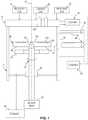
- FIG. 1illustrates a chemical vapor deposition apparatus in accordance with one embodiment of the invention.
- Reaction chamber 5defines a process environment space.
- Gas distribution device 10is arranged at one end of the chamber.
- the end having gas distribution device 10is referred to herein as the "top” end of reaction chamber 5.
- This end of the chambertypically, but not necessarily, is disposed at the top of the chamber in the normal gravitational frame of reference.
- the downward direction as used hereinrefers to the direction away from gas distribution device 10; whereas the upward direction refers to the direction within the chamber, toward gas distribution device 10, regardless of whether these directions are aligned with the gravitational upward and downward directions.
- the "top” and “bottom” surfaces of elementsare described herein with reference to the frame of reference of reaction chamber 5 and gas distribution device 10.
- Gas distribution device 10is connected to sources 15, 20, and 25 for supplying process gases to be used in the wafer treatment process, such as a carrier gas and reactant gases, such as a metalorganic compound and a source of a group V metal.
- Gas distribution device 10is arranged to receive the various gases and direct a flow of process gasses generally in the downward direction.
- Gas distribution device 10desirably is also connected to coolant system 30 arranged to circulate a liquid through gas distribution device 10 so as to maintain the temperature of the gas distribution device at a desired temperature during operation.
- a similar coolant arrangementcan be provided for cooling the walls of reaction chamber 5.
- Reaction chamber 5is also equipped with exhaust system 35 arranged to remove spent gases from the interior of the chamber through ports (not shown) at or near the bottom of the chamber so as to permit continuous flow of gas in the downward direction from gas distribution device 10.
- Spindle 40is arranged within the chamber so that the central axis 45 of spindle 40 extends in the upward and downward directions.
- Spindle 40is mounted to the chamber by a conventional rotary pass-through device 50 incorporating bearings and seals (not shown) so that spindle 40 can rotate about central axis 45, while maintaining a seal between spindle 40 and the wall of reaction chamber 5.
- the spindlehas fitting 55 at its top end, i.e., at the end of the spindle closest to gas distribution device 10.
- fitting 55is an example of a wafer carrier retention mechanism adapted to releasably engage a wafer carrier.
- fitting 55is a generally frustoconical element tapering toward the top end of the spindle and terminating at a flat top surface.
- a frustoconical elementis an element having the shape of a frustum of a cone.
- Spindle 40is connected to rotary drive mechanism 60 such as an electric motor drive, which is arranged to rotate spindle 40 about central axis 45.
- Heating element 65is mounted within the chamber and surrounds spindle 40 below fitting 55.
- Reaction chamber 5is also provided with entry opening 70 leading to antechamber 75, and door 80 for closing and opening the entry opening.
- Door 80is depicted only schematically in FIG. 1 , and is shown as movable between the closed position shown in solid lines, in which the door isolates the interior of reaction chamber 5 from antechamber 75, and an open position shown in broken lines at 80'.
- the door 80is equipped with an appropriate control and actuation mechanism for moving it between the open position and closed positions.
- the doormay include a shutter movable in the upward and downward directions as disclosed, for example, in U.S. Pat. No. 7,276,124 , the disclosure of which is hereby incorporated by reference herein.
- the apparatus depicted in FIG. 1may further include a loading mechanism (not shown) capable of moving a wafer carrier from the antechamber 75 into the chamber and engaging the wafer carrier with spindle 40 in the operative condition, and also capable of moving a wafer carrier off of spindle 40 and into antechamber 75.
- a loading mechanism(not shown) capable of moving a wafer carrier from the antechamber 75 into the chamber and engaging the wafer carrier with spindle 40 in the operative condition, and also capable of moving a wafer carrier off of spindle 40 and into antechamber 75.
- the apparatusalso includes a plurality of wafer carriers.
- a first wafer carrier 85is disposed inside reaction chamber 5 in an operative position, whereas a second wafer carrier 90 is disposed within antechamber 75.
- Each wafer carrierincludes body 95 which is substantially in the form of a circular disc having a central axis (See FIG. 2 ). Body 95 is formed symmetrically about central axis. In the operative position, the central axis of the wafer carrier body is coincident with central axis 45 of spindle 40. Body 95 may be formed as a single piece or as a composite of plural pieces. For example, as disclosed in U.S. Patent Application Pub. No.
- the wafer carrier bodymay include a hub defining a small region of the body surrounding the central axis and a larger portion defining the remainder of the disc-like body.
- Body 95is desirably formed from materials which do not contaminate the process and which can withstand the temperatures encountered in the process.
- the larger portion of the discmay be formed largely or entirely from materials such as graphite, silicon carbide, or other refractory materials.
- Body 95generally has a planar top surface 100 and a bottom surface 110 extending generally parallel to one another and generally perpendicular to the central axis of the disc.
- Body 95also has one, or a plurality, of wafer-holding features adapted to hold a plurality of wafers.
- wafer 115such as a disc-like wafer formed from sapphire, silicon carbide, or other crystalline substrate, is disposed within each pocket 120 of each wafer carrier.
- wafer 115has a thickness which is small in comparison to the dimensions of its major surfaces. For example, a circular wafer of about 2 inches (50 mm) in diameter may be about 430 ⁇ m thick or less.
- wafer 115is disposed with a top surface facing upwardly, so that the top surface is exposed at the top of the wafer carrier.
- wafer carrier 85carries different quantities of wafers. For instance, in one example embodiment, wafer carrier 85 can be adapted to hold six wafers. In another example embodiment, as shown in FIG. 2 , the wafer carrier holds 12 wafers.
- wafer carrier 85 with wafers loaded thereonis loaded from antechamber 75 into reaction chamber 5 and placed in the operative position shown in FIG. 1 . In this condition, the top surfaces of the wafers face upwardly, towards gas distribution device 10. Heating element 65 is actuated, and rotary drive mechanism 60 operates to turn spindle 40 and hence wafer carrier 85 around axis 45. Typically, spindle 40 is rotated at a rotational speed from about 50-1500 revolutions per minute. Process gas supply units 15, 20, and 25 are actuated to supply gases through gas distribution device 10.
- the gasespass downwardly toward wafer carrier 85, over top surface 100 of wafer carrier 85 and wafers 115, and downwardly around the periphery of the wafer carrier to the outlet and to exhaust system 50.
- the top surface of the wafer carrier and the top surfaces of wafer 115are exposed to a process gas including a mixture of the various gases supplied by the various process gas supply units.
- the process gas at the top surfaceis predominantly composed of the carrier gas supplied by carrier gas supply unit 20.
- the carrier gasmay be nitrogen, and hence the process gas at the top surface of the wafer carrier is predominantly composed of nitrogen with some amount of the reactive gas components.
- Heating elements 65transfer heat to the bottom surface 110 of wafer carrier 85, principally by radiant heat transfer.
- the heat applied to the bottom surface of wafer carrier 85flows upwardly through the body 95 of the wafer carrier to the top surface 100 of the wafer carrier. Heat passing upwardly through the body also passes upwardly through gaps to the bottom surface of each wafer, and upwardly through the wafer to the top surface of wafer 115.
- Heatis radiated from the top surface 100 of wafer carrier 85 and from the top surfaces of the wafer to the colder elements of the process chamber as, for example, to the walls of the process chamber and to gas distribution device 10. Heat is also transferred from the top surface 100 of wafer carrier 85 and the top surfaces of the wafers to the process gas passing over these surfaces.
- the systemincludes a number of features designed to determine uniformity of heating of the surfaces of each wafer 115.
- temperature profiling system 125receives temperature information that can include a temperature and temperature monitoring positional information from temperature monitor 130.
- temperature profiling system 125receives wafer carrier positional information, which in one embodiment can come from rotary drive mechanism 60. With this information, temperature profiling system 125 constructs a temperature profile of the wafers 120 on wafer carrier 85. The temperature profile represents a thermal distribution on the surface of each of the wafers 120.
- FIGS. 2 and 3illustrate wafer carrier 200, also referred to as a susceptor, in greater detail.
- Each wafer retention siteis in the form of a generally circular recess, or pocket 205, extending downwardly into body 210 from the top surface 215.
- FIG. 3is a cross-sectional view of pocket 205 (demarcated with a horizontal line and two angled arrow in FIG. 2 ).
- the generally circular shapeis made to correspond to the shape of wafer 240.
- Each wafer carrier 200includes body 210 which is substantially in the form of a circular disc having a central axis 220. Body 210 is formed symmetrically about central axis 220.
- each pocket 205has a floor surface 225 disposed below the surrounding portions of top surface 215.
- Each pocket 205also has a peripheral wall surface 230 surrounding floor surface 225 and defining the periphery of pocket 205.
- Peripheral wall surface 230extends downwardly from the top surface 215 of body 210 to floor surface 225.
- peripheral wall surface 230has an undercut where the wall slopes inwards, towards the center of the pocket, over at least a portion of the periphery.
- peripheral wall surface 230forms an acute angle relative to floor surface 225.
- the angle formed between peripheral wall surface 230 and floor surface 225is 80 degrees.
- portions of peripheral wall surface 230have varying degrees of sloping. For instance, in one such embodiment, those portions of peripheral wall surface 230 that are furthest from the central axis 220 of the wafer carrier have a more acute angle.
- the floor surface 225includes standoff features, such as tabs 235 located in certain locations along the periphery of each pocket 205. Tabs 235 raise the wafer 240 off of floor surface 225, thereby permitting some flow of gas around the edges and below the bottom surface of wafer 240.
- wafer 240can be raised from pocket floor surface 225 using a ring that fits inside pocket 205, just underneath peripheral wall surface 230; the ring can occupy the position of tabs 235 (i.e., in lieu of tabs), such that the outer periphery of wafer 240 rests on the ring.
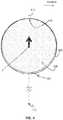
- FIG. 4is a partial plan view diagram of wafer 400 situated in a pocket 405, while the wafer carrier is rotating in the direction of rotation shown.
- each wafer 400 in its corresponding wafer pocket 405exerts a reactive centrifugal force outwardly along its corresponding wafer carrier radial axis 410 in response to the centripetal force applied to the wafer by the outer-most portion of peripheral wall surface of pocket 405.
- the reactive centrifugal forceis indicated with the arrow marked f that is pointing outwardly from central axis 415 along wafer carrier radial axis 410.
- wafer pocketsare circular, such that a wafer pocket has a single radius relative to the central axis of the pocket, as explained above in FIG. 4 .
- wafer pocketscan comprise different shapes.
- a wafer pocketcan be comprised of two or more arcs having different radii, such that the shape of the pocket can be elliptical or oval.
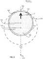
- wafer 500is situated in a pocket shaped from a compound radius of two intersecting arcs according to one type of embodiment.
- the radius 510 of first arc 515is smaller than radius 520 of second arc 525.
- First arc 515 and second arc 525 that together make up the periphery of the pocketare depicted in solid lines. For illustration purposes, these arcs are extended to form closed circles, with those portions not making up any part of the wafer pocket's periphery shown with dashed lines.
- First arc 515intersects with second arc 525 at intersection point 530.
- each wafer pocket of the wafer carrieris shaped from a compound radius of two intersecting arcs. In related embodiments, three or more arcs having different radii may form the shape of the pocket's periphery.
- such wafer pocketscan reduce the points of contact between a wafer and the interior portion of the wafer pocket against which the wafer presses (subject to centripetal force, or the reactive centrifugal force, during rotation of the wafer carrier, as depicted with arrow f ), as described above.
- using wafer pockets shaped as shown in FIG. 5can increase gap 535 between the interior wall of the wafer pocket and the peripheral edge of the wafer, as well as make gap 535 more uniform, as compared to a wafer pocket having a single curvature.
- thisensures better gas flow and reduces the temperature non-uniformities affecting the wafer during CVD processing.
- the wafer pocketis shaped such that, when the wafer is situated in the pocket during processing, gap 535 is generally uniform in size over a majority of the pocket's circumference.
- the generally uniform size of the gapis defined as a gap size having a tolerance of +/- 10%.
- gap 535is generally uniform over at least 66% of the circumference of the wafer retention pocket.
- gap 535is generally uniform over at least 75% of the circumference of the wafer retention pocket.
- the radiiare defined such that gap 535 is uniform over at least 85% of the circumference of the wafer retention pocket.
- a wafer pocketcan be shaped from a compound radius, such that the arcs corresponding to those radii do not naturally intersect (i.e., no intersection point).
- wafer 600is situated in a pocket shaped from a compound radius of two non-intersecting arcs according to one embodiment.
- the radius 610 of first arc 615is smaller than radius 620 of second arc 625; however, if extended to form closed circles (shown with dashed lines), first arc 615 would lie within second arc 625 and not intersect.
- wafer pocketscan be shaped from a compound radius of two or more non-intersecting arcs.
- a wafer pocket shaped from a compound radius of two non-intersecting arcsincludes connecting portions 640, symmetrically located on each side of the central axis 415 of the wafer pocket, and near the distal end of the wafer pocket against which the wafer presses (exerting centrifugal force, shown with arrow), as described above.
- Connecting portions 640complete the peripheral wall of the wafer pocket to connect first arc 615 and second arc 625.
- first arc 615 and second arc 625form a wafer pocket having a compound radius in which the arcs corresponding to each radius do not intersect (shown with solid lines).
- Such wafer pocketsincluding the wafer pockets shaped as shown in FIG. 6 , can reduce the points of contact between a wafer and the interior portion of the wafer pocket against which the wafer presses (exerting centrifugal force f), as described above. Additionally, using wafer pockets shaped as shown in FIG. 6 can increase gap 635 between the interior portion of the wafer pocket and the peripheral edge of the wafer, as well as make gap 635 more uniform, ultimately ensuring better gas flow and reducing the likelihood of forming temperature non-uniformities.
- the wafer pocketis shaped such that, when the wafer is situated in the pocket during processing, gap 635 is generally uniform in size over a majority of the pocket's circumference.
- the generally uniform size of the gapis defined as a gap size having a tolerance of +/- 10%.
- gap 635is generally uniform over at least 66% of the circumference of the wafer retention pocket.
- gap 635is generally uniform over at least 75% of the circumference of the wafer retention pocket.
- the radiiare defined such that gap 635 is uniform over at least 85% of the circumference of the wafer retention pocket.
- different wafer retention pocketscan have differing configurations of the compound radii defining the pockets.
- the ratio of the lengths of the first arc to the second arccan be different among wafer retention pockets that are situated closer to, or farther from, the center of the wafer carrier.
- the length of first arc 615can be in smaller proportion to the length of second arc 625 for those pockets which are closer to the center of the wafer carrier.
- the radii of the curvatures of the first and second arcscan vary from one wafer retention pocket to another on the same wafer carrier.
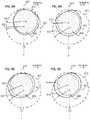
- each of the first and second arcs 515 and 525, or 615 and 625, respectivelyare situated symmetrically relative to wafer carrier radial axis 410.
- the arcsmay be situated asymmetrically to position the wafer somewhat off-center, which may further help mitigate heating non-uniformities in certain configurations.
- the centers of each of the first and second arcscan be situated such they both lie on the same wafer carrier radial axis 410.
- the arcsare extended to form closed circles, with those portions not making up any part of the wafer pocket's periphery shown with dashed lines.
- first arc 715 and second arc 725can also be symmetric with respect to the same wafer carrier radial axis 410, with radius 710 of first arc 715 being smaller than radius 720 of arc second 725 ( FIG. 7A ; see also, FIGS. 4-6 ).
- first arc 715can be symmetric with respect to wafer carrier radial axis 410
- second arc 725can be asymmetric with respect to wafer carrier radial axis 410, with radius 710 of first arc 715 being smaller than radius 720 of second arc 725 ( FIG. 7B ).
- first arc 715can be asymmetric with respect to wafer carrier radial axis 410 and second arc 725 can be symmetric with respect to wafer carrier radial axis 410, with radius 710 of first arc 715 being smaller than radius 720 of arc second 725 ( FIG. 7C ).
- first arc 715 and second arc 725can both be asymmetric with respect to wafer carrier radial axis 410, with radius 710 of first arc 715 being smaller than radius 720 of arc 725 ( FIG. 7D ).
- first and second arcscan be situated such they do not lie on the same wafer carrier radial axis.
- the arcsare extended to form closed circles, with those portions not making up any part of the wafer pocket's periphery shown with dashed lines.
- first arc 815 and second arc 825can be symmetric with respect to separate wafer carrier radial axes; for example, first arc 815 (with radius 810) can have a center that is not situated on wafer carrier radial axis 410, while second arc 825 (with radius 820) can have a center that is situated on wafer carrier radial axis 410 ( FIG.
- first arc 815(with radius 810) can be symmetric with respect to wafer carrier radial axis 410 and have a center situated on wafer carrier radial axis 410
- second arc 825(with radius 820) can be asymmetric with respect to wafer carrier radial axis 410 and have a center that is not situated on wafer carrier radial axis 410 ( FIG. 8B ).
- first arc 815(with radius 810) can be asymmetric with respect to wafer carrier radial axis 410 but have a center situated on wafer carrier radial axis 410
- second arc 825(with radius 820) can be symmetric with respect to a separate wafer carrier axis (i.e., not wafer carrier radial axis 410) and have a center not situated on wafer carrier radial axis 410 ( FIG. 8C ).
- first arc 815 (with radius 810) and second arc 825 (with radius 820)can both be asymmetric with respect to separate wafer carrier axes (e.g., wafer carrier radial axis 410 and a separate wafer radial carrier axis) and both can have centers situated on separate radial axes (e.g., wafer carrier radial axis 410 and a separate wafer radial carrier axis) ( FIG. 8D ).
- wafer carrier axese.g., wafer carrier radial axis 410 and a separate wafer radial carrier axis
- FIG. 8Dseparate wafer radial carrier axis
Landscapes
- Chemical & Material Sciences (AREA)
- Engineering & Computer Science (AREA)
- General Chemical & Material Sciences (AREA)
- Chemical Kinetics & Catalysis (AREA)
- Materials Engineering (AREA)
- Metallurgy (AREA)
- Organic Chemistry (AREA)
- Mechanical Engineering (AREA)
- Crystallography & Structural Chemistry (AREA)
- Physics & Mathematics (AREA)
- Condensed Matter Physics & Semiconductors (AREA)
- General Physics & Mathematics (AREA)
- Manufacturing & Machinery (AREA)
- Computer Hardware Design (AREA)
- Microelectronics & Electronic Packaging (AREA)
- Power Engineering (AREA)
- Chemical Vapour Deposition (AREA)
- Container, Conveyance, Adherence, Positioning, Of Wafer (AREA)
Description
- The invention relates generally to semiconductor fabrication technology and, more particularly, to chemical vapor deposition (CVD) processing and associated apparatus having features for reducing temperature non-uniformities on semiconductor wafer surfaces during processing.
- In the fabrication of light-emitting diodes (LEDs) and other high-performance devices such as laser diodes, optical detectors, and field effect transistors, a chemical vapor deposition (CVD) process is typically used to grow a thin film stack structure using materials such as gallium nitride over a sapphire or silicon substrate. A CVD tool includes a process chamber, which is a sealed environment that allows infused gases to be deposited upon the substrate (typically in the form of wafers) to grow the thin film layers. An example of a current product line of such manufacturing equipment is the TurboDisc® family of MOCVD systems, manufactured by Veeco Instruments Inc. of Plainview, New York.
- A number of process parameters are controlled, such as temperature, pressure and gas flow rate, to achieve a desired crystal growth. Different layers are grown using varying materials and process parameters. For example, devices formed from compound semiconductors such as III-V semiconductors typically are formed by growing successive layers of the compound semiconductor using metal organic chemical vapor deposition (MOCVD). In this process, the wafers are exposed to a combination of gases, typically including a metal organic compound as a source of a group III metal, and also including a source of a group V element which flow over the surface of the wafer while the wafer is maintained at an elevated temperature. Generally, the metal organic compound and group V source are combined with a carrier gas which does not participate appreciably in the reaction as, for example, nitrogen. One example of a III-V semiconductor is gallium nitride, which can be formed by reaction of an organo-gallium compound and ammonia on a substrate having a suitable crystal lattice spacing, as for example, a sapphire wafer. The wafer is usually maintained at a temperature on the order of 1000-1100°C during deposition of gallium nitride and related compounds.
- In a MOCVD process, where the growth of crystals occurs by chemical reaction on the surface of the substrate, the process parameters must be controlled with particular care to ensure that the chemical reaction proceeds under the required conditions. Even small variations in process conditions can adversely affect device quality and production yield. For instance, if a gallium and indium nitride layer is deposited, variations in wafer surface temperature will cause variations in the composition and bandgap of the deposited layer. Because indium has a relatively high vapor pressure, the deposited layer will have a lower proportion of indium and a greater bandgap in those regions of the wafer where the surface temperature is higher. If the deposited layer is an active, light-emitting layer of an LED structure, the emission wavelength of the LEDs formed from the wafer will also vary to an unacceptable degree.
- In a MOCVD process chamber, semiconductor wafers on which layers of thin film are to be grown are placed on rapidly-rotating carousels, referred to as wafer carriers, to provide a uniform exposure of their surfaces to the atmosphere within the reactor chamber for the deposition of the semiconductor materials. Rotation speed is on the order of 1,000 RPM. The wafer carriers are typically machined out of a highly thermally conductive material such as graphite, and are often coated with a protective layer of a material such as silicon carbide. Each wafer carrier has a set of circular indentations, or pockets, in its top surface in which individual wafers are placed. Typically, the wafers are supported in spaced relationship to the bottom surface of each of the pockets to permit the flow of gas around the edges of the wafer. Some examples of pertinent technology are described in
U.S. Patent Application Publication No. 2012/0040097 ,U.S. Patent No. 8,092,599 ,U.S. Patent No. 8,021,487 ,U.S. Patent Application Publication No. 2007/0186853 ,U.S. Patent No. 6,902,623 ,U.S. Patent No. 6,506,252 , andU.S. Patent No. 6,492,625 . - The wafer carrier is supported on a spindle within the reaction chamber so that the top surface of the wafer carrier having the exposed surfaces of the wafers faces upwardly toward a gas distribution device. While the spindle is rotated, the gas is directed downwardly onto the top surface of the wafer carrier and flows across the top surface toward the periphery of the wafer carrier. The used gas is evacuated from the reaction chamber through ports disposed below the wafer carrier. The wafer carrier is maintained at the desired elevated temperature by heating elements, typically electrical resistive heating elements disposed below the bottom surface of the wafer carrier. These heating elements are maintained at a temperature above the desired temperature of the wafer surfaces, whereas the gas distribution device typically is maintained at a temperature well below the desired reaction temperature so as to prevent premature reaction of the gases. Therefore, heat is transferred from the heating elements to the bottom surface of the wafer carrier and flows upwardly through the wafer carrier to the individual wafers.
- The gas flow over the wafers varies depending on the radial position of each wafer, with outermost-positioned wafers being subjected to higher flow rates due to their faster velocity during rotation. Even each individual wafer can have temperature non-uniformities, i.e., cold spots and hot spots depending upon its geometrical position relative to the other wafers on the carrier. One of the variables affecting the formation of temperature non-uniformities is the shape of the pockets within the wafer carrier. Generally, pocket shapes are circular and have a single radius of curvature. As the wafer carrier rotates, the wafers are subject to substantial centripetal force at their outermost edge (i.e., the furthermost edge from the axis of rotation), causing the wafer to press against the interior wall of the respective pocket in the wafer carrier. Under this condition, there is no gas flow around these outer edges of the wafers, and there is increased heat conduction to these outer-most portions of the wafers, resulting in more temperature non-uniformity and further aggravating the problems described above. Efforts have been made to minimize the temperature non-uniformities by increasing the gap between the wafer's edge and the interior wall of the pocket, including designing a wafer that is flat on a portion of the edge (i.e., a "flat" wafer). This flat portion of the wafer creates a gap for gas to flow and decreases the points of contact with the interior wall of the pocket, thereby mitigating temperature non-uniformities.
A great deal of effort has been devoted to system design features to minimize temperature variations during processing; however, the problem continues to present many challenges. Given the extreme conditions wafers are subject to during chemical vapor deposition, including exposure to substantial centripetal force, there remains a need for improved technologies to further reduce temperature non-uniformities.US 2010/0055318 A1 andUS 2013/0065403 A1 disclose wafer carriers. - The invention provides a wafer carrier as set forth in
claim 1; and a method for constructing a wafer carrier as set forth inclaim 15. Particular embodiments of the invention are disclosed in claims 2-14. One aspect is directed to a wafer carrier for use in a system for growing epitaxial layers on one or more wafers by chemical vapor deposition (CVD). The wafer carrier includes a body formed symmetrically about a central axis, and including a generally planar top surface that is situated perpendicularly to the central axis. A plurality of wafer retention pockets are recessed in the body from the top surface, each of the wafer retention pockets including a floor surface generally parallel to the top surface, and a peripheral wall surface that surrounds the floor surface and defines a periphery of that wafer retention pocket. Each wafer retention pocket has a pocket center situated along a corresponding wafer carrier radial axis that is perpendicular to the central axis. Each wafer retention pocket has a periphery having a shape defined by at least a first arc having a first radius of curvature situated around a first arc center and a second arc having a second radius of curvature situated around a second arc center. The second arc is different from the first arc by at least one of: the first radius of curvature being different from the second radius of curvature, or the first arc center being different from the second arc center. - Advantageously, the use of wafer retention pockets shaped from compound arcs having different radii of curvature can provide improved uniformity in the thermal distribution on the surface of a wafer subjected to a CVD process. A number of other advantages will become apparent from the following Detailed Description.
- The invention may be more completely understood in consideration of the following detailed description of various embodiments of the invention in connection with the accompanying drawings, in which:
FIG. 1 illustrates a chemical vapor deposition apparatus in accordance with one embodiment of the invention.FIG. 2 is a perspective view diagram illustrating a wafer carrier used with a CVD system, according to one embodiment of the invention.FIG. 3 is a diagram of a cross-sectional view taken along the line shown, detailing a wafer pocket used with a CVD system, according to one embodiment of the invention.FIG. 4 is a diagram of a wafer situated in a conventional pocket, according to one embodiment of the invention.FIG. 5 is a diagram of a wafer situated in a pocket shaped from a compound radius of two intersecting arcs, according to one embodiment of the invention.FIG. 6 is a diagram of a wafer situated in a pocket shaped from a compound radius of two non-intersecting arcs, according to one embodiment of the invention.FIGS. 7A-7D are diagrams of wafers situated in pockets shaped from compound radii of two arcs, according to embodiments of the invention.FIGS. 8A-8D are diagrams of wafers situated in pockets shaped from compound radii of two arcs, according to embodiments of the invention.- While the invention is amenable to various modifications and alternative forms, specifics thereof have been shown by way of example in the drawings and will be described in detail. It should be understood, however, that the intention is not to limit the invention to the particular embodiments described. On the contrary, the intention is to cover all modifications, equivalents, and alternatives falling within the scope of the invention as defined by the appended claims.
FIG. 1 illustrates a chemical vapor deposition apparatus in accordance with one embodiment of the invention.Reaction chamber 5 defines a process environment space.Gas distribution device 10 is arranged at one end of the chamber. The end havinggas distribution device 10 is referred to herein as the "top" end ofreaction chamber 5. This end of the chamber typically, but not necessarily, is disposed at the top of the chamber in the normal gravitational frame of reference. Thus, the downward direction as used herein refers to the direction away fromgas distribution device 10; whereas the upward direction refers to the direction within the chamber, towardgas distribution device 10, regardless of whether these directions are aligned with the gravitational upward and downward directions. Similarly, the "top" and "bottom" surfaces of elements are described herein with reference to the frame of reference ofreaction chamber 5 andgas distribution device 10.Gas distribution device 10 is connected tosources Gas distribution device 10 is arranged to receive the various gases and direct a flow of process gasses generally in the downward direction.Gas distribution device 10 desirably is also connected tocoolant system 30 arranged to circulate a liquid throughgas distribution device 10 so as to maintain the temperature of the gas distribution device at a desired temperature during operation. A similar coolant arrangement (not shown) can be provided for cooling the walls ofreaction chamber 5.Reaction chamber 5 is also equipped withexhaust system 35 arranged to remove spent gases from the interior of the chamber through ports (not shown) at or near the bottom of the chamber so as to permit continuous flow of gas in the downward direction fromgas distribution device 10.Spindle 40 is arranged within the chamber so that thecentral axis 45 ofspindle 40 extends in the upward and downward directions.Spindle 40 is mounted to the chamber by a conventional rotary pass-throughdevice 50 incorporating bearings and seals (not shown) so thatspindle 40 can rotate aboutcentral axis 45, while maintaining a seal betweenspindle 40 and the wall ofreaction chamber 5. The spindle has fitting 55 at its top end, i.e., at the end of the spindle closest togas distribution device 10. As further discussed below, fitting 55 is an example of a wafer carrier retention mechanism adapted to releasably engage a wafer carrier. In the particular embodiment depicted, fitting 55 is a generally frustoconical element tapering toward the top end of the spindle and terminating at a flat top surface. A frustoconical element is an element having the shape of a frustum of a cone.Spindle 40 is connected torotary drive mechanism 60 such as an electric motor drive, which is arranged to rotatespindle 40 aboutcentral axis 45.Heating element 65 is mounted within the chamber and surroundsspindle 40 below fitting 55.Reaction chamber 5 is also provided with entry opening 70 leading toantechamber 75, anddoor 80 for closing and opening the entry opening.Door 80 is depicted only schematically inFIG. 1 , and is shown as movable between the closed position shown in solid lines, in which the door isolates the interior ofreaction chamber 5 fromantechamber 75, and an open position shown in broken lines at 80'. Thedoor 80 is equipped with an appropriate control and actuation mechanism for moving it between the open position and closed positions. In practice, the door may include a shutter movable in the upward and downward directions as disclosed, for example, inU.S. Pat. No. 7,276,124 , the disclosure of which is hereby incorporated by reference herein. The apparatus depicted inFIG. 1 may further include a loading mechanism (not shown) capable of moving a wafer carrier from theantechamber 75 into the chamber and engaging the wafer carrier withspindle 40 in the operative condition, and also capable of moving a wafer carrier off ofspindle 40 and intoantechamber 75.- The apparatus also includes a plurality of wafer carriers. In the operating condition shown in
FIG. 1 , afirst wafer carrier 85 is disposed insidereaction chamber 5 in an operative position, whereas asecond wafer carrier 90 is disposed withinantechamber 75. Each wafer carrier includesbody 95 which is substantially in the form of a circular disc having a central axis (SeeFIG. 2 ).Body 95 is formed symmetrically about central axis. In the operative position, the central axis of the wafer carrier body is coincident withcentral axis 45 ofspindle 40.Body 95 may be formed as a single piece or as a composite of plural pieces. For example, as disclosed inU.S. Patent Application Pub. No. 20090155028 , the disclosure of which is hereby incorporated by reference herein, the wafer carrier body may include a hub defining a small region of the body surrounding the central axis and a larger portion defining the remainder of the disc-like body.Body 95 is desirably formed from materials which do not contaminate the process and which can withstand the temperatures encountered in the process. For example, the larger portion of the disc may be formed largely or entirely from materials such as graphite, silicon carbide, or other refractory materials.Body 95 generally has a planartop surface 100 and abottom surface 110 extending generally parallel to one another and generally perpendicular to the central axis of the disc.Body 95 also has one, or a plurality, of wafer-holding features adapted to hold a plurality of wafers. - In operation,
wafer 115, such as a disc-like wafer formed from sapphire, silicon carbide, or other crystalline substrate, is disposed within eachpocket 120 of each wafer carrier. Typically,wafer 115 has a thickness which is small in comparison to the dimensions of its major surfaces. For example, a circular wafer of about 2 inches (50 mm) in diameter may be about 430 µm thick or less. As illustrated inFIG. 1 ,wafer 115 is disposed with a top surface facing upwardly, so that the top surface is exposed at the top of the wafer carrier. It should be noted that in various embodiments,wafer carrier 85 carries different quantities of wafers. For instance, in one example embodiment,wafer carrier 85 can be adapted to hold six wafers. In another example embodiment, as shown inFIG. 2 , the wafer carrier holds 12 wafers. - In a typical MOCVD process,
wafer carrier 85 with wafers loaded thereon is loaded fromantechamber 75 intoreaction chamber 5 and placed in the operative position shown inFIG. 1 . In this condition, the top surfaces of the wafers face upwardly, towardsgas distribution device 10.Heating element 65 is actuated, androtary drive mechanism 60 operates to turnspindle 40 and hencewafer carrier 85 aroundaxis 45. Typically,spindle 40 is rotated at a rotational speed from about 50-1500 revolutions per minute. Processgas supply units gas distribution device 10. The gases pass downwardly towardwafer carrier 85, overtop surface 100 ofwafer carrier 85 andwafers 115, and downwardly around the periphery of the wafer carrier to the outlet and toexhaust system 50. Thus, the top surface of the wafer carrier and the top surfaces ofwafer 115 are exposed to a process gas including a mixture of the various gases supplied by the various process gas supply units. Most typically, the process gas at the top surface is predominantly composed of the carrier gas supplied by carrier gas supply unit 20. In a typical chemical vapor deposition process, the carrier gas may be nitrogen, and hence the process gas at the top surface of the wafer carrier is predominantly composed of nitrogen with some amount of the reactive gas components. Heating elements 65 transfer heat to thebottom surface 110 ofwafer carrier 85, principally by radiant heat transfer. The heat applied to the bottom surface ofwafer carrier 85 flows upwardly through thebody 95 of the wafer carrier to thetop surface 100 of the wafer carrier. Heat passing upwardly through the body also passes upwardly through gaps to the bottom surface of each wafer, and upwardly through the wafer to the top surface ofwafer 115. Heat is radiated from thetop surface 100 ofwafer carrier 85 and from the top surfaces of the wafer to the colder elements of the process chamber as, for example, to the walls of the process chamber and togas distribution device 10. Heat is also transferred from thetop surface 100 ofwafer carrier 85 and the top surfaces of the wafers to the process gas passing over these surfaces.- In the embodiment depicted, the system includes a number of features designed to determine uniformity of heating of the surfaces of each
wafer 115. In this embodiment,temperature profiling system 125 receives temperature information that can include a temperature and temperature monitoring positional information fromtemperature monitor 130. In addition,temperature profiling system 125 receives wafer carrier positional information, which in one embodiment can come fromrotary drive mechanism 60. With this information,temperature profiling system 125 constructs a temperature profile of thewafers 120 onwafer carrier 85. The temperature profile represents a thermal distribution on the surface of each of thewafers 120. FIGS. 2 and 3 illustratewafer carrier 200, also referred to as a susceptor, in greater detail. Each wafer retention site is in the form of a generally circular recess, orpocket 205, extending downwardly intobody 210 from thetop surface 215.FIG. 3 is a cross-sectional view of pocket 205 (demarcated with a horizontal line and two angled arrow inFIG. 2 ). The generally circular shape is made to correspond to the shape ofwafer 240. Eachwafer carrier 200 includesbody 210 which is substantially in the form of a circular disc having acentral axis 220.Body 210 is formed symmetrically aboutcentral axis 220. In the operative position, thecentral axis 220 ofwafer carrier body 210 is coincident with the axis of the spindle (SeeFIG. 3 ).Body 210 may be formed as a single piece or as a composite of plural pieces. Eachpocket 205 has afloor surface 225 disposed below the surrounding portions oftop surface 215. Eachpocket 205 also has aperipheral wall surface 230 surroundingfloor surface 225 and defining the periphery ofpocket 205.Peripheral wall surface 230 extends downwardly from thetop surface 215 ofbody 210 tofloor surface 225. In various embodiments, as depicted in particular inFIG. 3 ,peripheral wall surface 230 has an undercut where the wall slopes inwards, towards the center of the pocket, over at least a portion of the periphery. Thus,peripheral wall surface 230 forms an acute angle relative tofloor surface 225. In one example embodiment, the angle formed betweenperipheral wall surface 230 andfloor surface 225 is 80 degrees.- In a related embodiment (not shown), portions of
peripheral wall surface 230 have varying degrees of sloping. For instance, in one such embodiment, those portions ofperipheral wall surface 230 that are furthest from thecentral axis 220 of the wafer carrier have a more acute angle. In another related embodiment, as illustrated inFIG. 3 , thefloor surface 225 includes standoff features, such astabs 235 located in certain locations along the periphery of eachpocket 205.Tabs 235 raise thewafer 240 off offloor surface 225, thereby permitting some flow of gas around the edges and below the bottom surface ofwafer 240. In other embodiments,wafer 240 can be raised frompocket floor surface 225 using a ring that fits insidepocket 205, just underneathperipheral wall surface 230; the ring can occupy the position of tabs 235 (i.e., in lieu of tabs), such that the outer periphery ofwafer 240 rests on the ring. FIG. 4 is a partial plan view diagram ofwafer 400 situated in apocket 405, while the wafer carrier is rotating in the direction of rotation shown. When a wafer carrier is rotating, eachwafer 400 in itscorresponding wafer pocket 405 exerts a reactive centrifugal force outwardly along its corresponding wafercarrier radial axis 410 in response to the centripetal force applied to the wafer by the outer-most portion of peripheral wall surface ofpocket 405. The reactive centrifugal force is indicated with the arrow markedf that is pointing outwardly fromcentral axis 415 along wafercarrier radial axis 410. As a result, an increasedsized gap 420 is created on the interior portion, and the outer portion ofwafer 400 presses against the interior wall ofpocket 405. This situation creates temperature non-uniformities, with the outer portion being subjected generally to increased localized temperatures, i.e., hot spots.- Generally, the shapes of wafer pockets are circular, such that a wafer pocket has a single radius relative to the central axis of the pocket, as explained above in
FIG. 4 . However, in an effort to maintain a more uniform gap between a wafer and the peripheral wall of a wafer pocket to allow a more even distribution of gases during the CVD process, ultimately reducing temperature non-uniformities, wafer pockets can comprise different shapes. In various embodiments, a wafer pocket can be comprised of two or more arcs having different radii, such that the shape of the pocket can be elliptical or oval. - As illustrated in
FIG. 5 ,wafer 500 is situated in a pocket shaped from a compound radius of two intersecting arcs according to one type of embodiment. Theradius 510 offirst arc 515 is smaller thanradius 520 ofsecond arc 525.First arc 515 andsecond arc 525 that together make up the periphery of the pocket are depicted in solid lines. For illustration purposes, these arcs are extended to form closed circles, with those portions not making up any part of the wafer pocket's periphery shown with dashed lines.First arc 515 intersects withsecond arc 525 atintersection point 530. In the embodiment depicted, each wafer pocket of the wafer carrier is shaped from a compound radius of two intersecting arcs. In related embodiments, three or more arcs having different radii may form the shape of the pocket's periphery. - According to these embodiments, such wafer pockets, can reduce the points of contact between a wafer and the interior portion of the wafer pocket against which the wafer presses (subject to centripetal force, or the reactive centrifugal force, during rotation of the wafer carrier, as depicted with arrowf), as described above. Additionally, using wafer pockets shaped as shown in
FIG. 5 can increasegap 535 between the interior wall of the wafer pocket and the peripheral edge of the wafer, as well asmake gap 535 more uniform, as compared to a wafer pocket having a single curvature. Advantageously, this ensures better gas flow and reduces the temperature non-uniformities affecting the wafer during CVD processing. - In one embodiment, the wafer pocket is shaped such that, when the wafer is situated in the pocket during processing,
gap 535 is generally uniform in size over a majority of the pocket's circumference. In this context, the generally uniform size of the gap is defined as a gap size having a tolerance of +/- 10%. In a related embodiment,gap 535 is generally uniform over at least 66% of the circumference of the wafer retention pocket. In still another related embodiment,gap 535 is generally uniform over at least 75% of the circumference of the wafer retention pocket. In a further embodiment, the radii are defined such thatgap 535 is uniform over at least 85% of the circumference of the wafer retention pocket. - In other embodiments, a wafer pocket can be shaped from a compound radius, such that the arcs corresponding to those radii do not naturally intersect (i.e., no intersection point). As shown in
FIG. 6 ,wafer 600 is situated in a pocket shaped from a compound radius of two non-intersecting arcs according to one embodiment. Theradius 610 offirst arc 615 is smaller thanradius 620 ofsecond arc 625; however, if extended to form closed circles (shown with dashed lines),first arc 615 would lie withinsecond arc 625 and not intersect. In some embodiments, wafer pockets can be shaped from a compound radius of two or more non-intersecting arcs. In related embodiments, a wafer pocket shaped from a compound radius of two non-intersecting arcs includes connectingportions 640, symmetrically located on each side of thecentral axis 415 of the wafer pocket, and near the distal end of the wafer pocket against which the wafer presses (exerting centrifugal force, shown with arrow), as described above. Connectingportions 640 complete the peripheral wall of the wafer pocket to connectfirst arc 615 andsecond arc 625. - As shown in
FIG. 6 ,first arc 615 andsecond arc 625 form a wafer pocket having a compound radius in which the arcs corresponding to each radius do not intersect (shown with solid lines). Such wafer pockets, including the wafer pockets shaped as shown inFIG. 6 , can reduce the points of contact between a wafer and the interior portion of the wafer pocket against which the wafer presses (exerting centrifugal force f), as described above. Additionally, using wafer pockets shaped as shown inFIG. 6 can increasegap 635 between the interior portion of the wafer pocket and the peripheral edge of the wafer, as well asmake gap 635 more uniform, ultimately ensuring better gas flow and reducing the likelihood of forming temperature non-uniformities. - In one embodiment, the wafer pocket is shaped such that, when the wafer is situated in the pocket during processing,
gap 635 is generally uniform in size over a majority of the pocket's circumference. In this context, the generally uniform size of the gap is defined as a gap size having a tolerance of +/- 10%. In a related embodiment,gap 635 is generally uniform over at least 66% of the circumference of the wafer retention pocket. In still another related embodiment,gap 635 is generally uniform over at least 75% of the circumference of the wafer retention pocket. In a further embodiment, the radii are defined such thatgap 635 is uniform over at least 85% of the circumference of the wafer retention pocket. - The embodiments above are intended to be illustrative and not limiting. Other variations are contemplated to fall within the claims. For example, in a related embodiment, on a given wafer carrier, different wafer retention pockets can have differing configurations of the compound radii defining the pockets. For example, in one embodiment, the ratio of the lengths of the first arc to the second arc can be different among wafer retention pockets that are situated closer to, or farther from, the center of the wafer carrier. For instance, the length of
first arc 615 can be in smaller proportion to the length ofsecond arc 625 for those pockets which are closer to the center of the wafer carrier. It is also contemplated that the opposite configuration (i.e., thefirst arc 615 being in larger proportion) for the pockets that are closer to the center, in certain other embodiments. Similar arrangements can be made forarcs FIG. 5 . - In another type of variation, the radii of the curvatures of the first and second arcs can vary from one wafer retention pocket to another on the same wafer carrier.
- In still another type of variation, each of the first and
second arcs carrier radial axis 410. In another embodiment, the arcs may be situated asymmetrically to position the wafer somewhat off-center, which may further help mitigate heating non-uniformities in certain configurations. For example, as shown inFIGS. 7A-D , the centers of each of the first and second arcs can be situated such they both lie on the same wafercarrier radial axis 410. For illustration purposes, the arcs are extended to form closed circles, with those portions not making up any part of the wafer pocket's periphery shown with dashed lines. In some cases,first arc 715 andsecond arc 725 can also be symmetric with respect to the same wafercarrier radial axis 410, withradius 710 offirst arc 715 being smaller thanradius 720 of arc second 725 (FIG. 7A ; see also,FIGS. 4-6 ). In other cases,first arc 715 can be symmetric with respect to wafercarrier radial axis 410, andsecond arc 725 can be asymmetric with respect to wafercarrier radial axis 410, withradius 710 offirst arc 715 being smaller thanradius 720 of second arc 725 (FIG. 7B ). In other cases,first arc 715 can be asymmetric with respect to wafercarrier radial axis 410 andsecond arc 725 can be symmetric with respect to wafercarrier radial axis 410, withradius 710 offirst arc 715 being smaller thanradius 720 of arc second 725 (FIG. 7C ). In still other cases,first arc 715 andsecond arc 725 can both be asymmetric with respect to wafercarrier radial axis 410, withradius 710 offirst arc 715 being smaller thanradius 720 of arc 725 (FIG. 7D ). - Additionally, as shown in
FIGS. 8A-D , the centers of each of the first and second arcs can be situated such they do not lie on the same wafer carrier radial axis. For illustration purposes, the arcs are extended to form closed circles, with those portions not making up any part of the wafer pocket's periphery shown with dashed lines. In some cases,first arc 815 andsecond arc 825 can be symmetric with respect to separate wafer carrier radial axes; for example, first arc 815 (with radius 810) can have a center that is not situated on wafercarrier radial axis 410, while second arc 825 (with radius 820) can have a center that is situated on wafer carrier radial axis 410 (FIG. 8A ). In other cases, first arc 815 (with radius 810) can be symmetric with respect to wafercarrier radial axis 410 and have a center situated on wafercarrier radial axis 410, while second arc 825 (with radius 820) can be asymmetric with respect to wafercarrier radial axis 410 and have a center that is not situated on wafer carrier radial axis 410 (FIG. 8B ). In other cases, first arc 815 (with radius 810) can be asymmetric with respect to wafercarrier radial axis 410 but have a center situated on wafercarrier radial axis 410, while second arc 825 (with radius 820) can be symmetric with respect to a separate wafer carrier axis (i.e., not wafer carrier radial axis 410) and have a center not situated on wafer carrier radial axis 410 (FIG. 8C ). In still other cases, first arc 815 (with radius 810) and second arc 825 (with radius 820) can both be asymmetric with respect to separate wafer carrier axes (e.g., wafercarrier radial axis 410 and a separate wafer radial carrier axis) and both can have centers situated on separate radial axes (e.g., wafercarrier radial axis 410 and a separate wafer radial carrier axis) (FIG. 8D ). These and other variations may help further mitigate temperature non-uniformities occurring onwafer 800. - In addition, although aspects of the present invention have been described with reference to particular embodiments, those skilled in the art will recognize that changes can be made in form and detail without departing from the scope of the invention, as defined by the claims. Persons of ordinary skill in the relevant arts will recognize that the invention may comprise fewer features than illustrated in any individual embodiment described above. The embodiments described herein are not meant to be an exhaustive presentation of the ways in which the various features of the invention may be combined. Accordingly, the embodiments are not mutually exclusive combinations of features; rather, the invention may comprise a combination of different individual features selected from different individual embodiments, as will be understood by persons of ordinary skill in the art.
Claims (15)
- A wafer carrier (200) for use in a system for growing epitaxial layers on one or more wafers by chemical vapor deposition (CVD), the wafer carrier comprising:a body formed symmetrically about a central axis (45), and including a generally planar top surface that is perpendicular to the central axis (45);a plurality of wafer retention pockets (205) recessed in the body from the top surface, each of the wafer retention pockets (205) including:a floor surface generally parallel to the top surface; anda peripheral wall surface surrounding the floor surface and defining a periphery of that wafer retention pocket,wherein each wafer retention pocket (205) has a pocket center situated along a corresponding wafer carrier radial axis that is perpendicular to the central axis (45); andfor each wafer retention pocket (205), a first arc (515) having a first radius of curvature is defined around a first arc center and a second arc (525) having a second radius of curvature is defined around a second arc center, and the periphery corresponding to the wafer retention pocket is entirely defined by the portions of the first arc (515) that are closer to the pocket center along any given radial line than the second arc (525) and the portions of the second arc (525) that are closer to the pocket center along any given radial line than the first arc (515), wherein the second arc (525) is different from the first arc (515) by at least one of:the first radius of curvature being different from the second radius of curvature; andthe first arc center being different from the second arc center.
- The wafer carrier of claim 1, wherein in the periphery of each wafer retention pocket (205), the first arc (515) and the second arc (525) intersect.
- The wafer carrier of claim 1, wherein in the periphery of each wafer retention pocket (205), the first arc (515) and the second arc (525) do not intersect.
- The wafer carrier of claim 1, wherein each wafer retention pocket (205) has a proximal end and a distal end relative to the central axis (45), and in the periphery of each wafer retention pocket (205), the first arc (515) is situated at the distal end and the second arc (525) is situated at the proximal end;
wherein the first arc (525) has a smaller radius of curvature than the second arc (525). - The wafer carrier of claim 1, wherein each wafer retention pocket (205) has a proximal end and a distal end relative to the central axis (45), and in the periphery of each wafer retention pocket (205), the first arc (515) is situated at the distal end and the second arc (525) is situated at the proximal end;
wherein the first arc (515) has a larger radius of curvature than the second arc (525). - The wafer carrier of claim 1, wherein each wafer retention pocket (205) has a proximal end and a distal end relative to the central axis (45), and in the periphery of each wafer retention pocket (205), the first arc (515) is situated at the distal end and the second arc (525) is situated at the proximal end;
wherein the first arc (515) is situated symmetrically about the wafer carrier radial axis corresponding to the wafer retention pocket (205) having the periphery defined by the first and the second arcs (515, 525). - The wafer carrier of claim 1, wherein each wafer retention pocket (205) has a proximal end and a distal end relative to the central axis (45), and in the periphery of each wafer retention pocket (205), the first arc (515) is situated at the distal end and the second arc (525) is situated at the proximal end;
wherein the second arc (525) is situated symmetrically about the wafer carrier radial axis corresponding to the wafer retention pocket (205) having the periphery defined by the first and the second arcs (515, 525). - The wafer carrier of claim 1, wherein each wafer retention pocket (205) has a proximal end and a distal end relative to the central axis (45), and in the periphery of each wafer retention pocket (205), the first arc (515) is situated at the distal end and the second arc (525) is situated at the proximal end;
wherein the first arc (515) and the second arc (525) are each situated symmetrically about the wafer carrier radial axis corresponding to the wafer retention pocket (205) having the periphery defined by the first and the second arcs (515, 525). - The wafer carrier of claim 1, wherein each wafer retention pocket (205) has a proximal end and a distal end relative to the central axis (45), and in the periphery of each wafer retention pocket (205), the first arc (515) is situated at the distal end and the second arc (525) is situated at the proximal end;
wherein the first arc (515) is situated asymmetrically about the wafer carrier radial axis corresponding to the wafer retention pocket (205) having the periphery defined by the first and the second arcs (515, 525). - The wafer carrier of claim 1, wherein each wafer retention pocket (205) has a proximal end and a distal end relative to the central axis (45), and in the periphery of each wafer retention pocket (205), the first arc (515) is situated at the distal end and the second arc (525) is situated at the proximal end;
wherein the first arc (515) and/or the second arc (525) is/are situated asymmetrically about the wafer carrier radial axis corresponding to the wafer retention pocket having the periphery defined by the first and the second arcs (515, 525). - The wafer carrier of claim 1, wherein the shape of the periphery of each wafer retention pocket (205) is further defined by at least one connecting portion that intersects with both the first arc and the second arc (515, 525); or
wherein the shape of the periphery of each wafer retention pocket (205) is further defined by two connecting portions that each intersects with both the first arc and the second arc (515, 525). - The wafer carrier of claim 1, further comprising:
a first wafer retention pocket and a second wafer retention pocket; and
wherein a ratio between a length of the first arc to a length of the second arc of a common wafer retention pocket is different among the first wafer retention pocket and the second wafer retention pocket. - The wafer carrier of claim 1, further comprising:
a first wafer retention pocket and a second wafer retention pocket; and
wherein a ratio between a radius of curvature of the first arc to a radius of curvature of the second arc of a common wafer retention pocket is different among the first wafer retention pocket and the second wafer retention pocket. - The wafer carrier of claim 1, wherein the periphery of each wafer retention pocket is constructed such that, when a wafer (500) is situated in the wafer retention pocket (205) during CVD processing, a gap between an outer edge of the wafer (500) and the periphery of the wafer retention pocket (205) is generally uniform in size around at least 50% or at least 75% of a circumference of the wafer (500).
- A method for constructing a wafer carrier (200) for use in a system for growing epitaxial layers on one or more wafers by chemical vapor deposition (CVD), the method comprising:forming a body symmetrically about a central axis (45) to include a generally planar top surface that is perpendicular to the central axis (45);forming a plurality of wafer retention pockets (205) recessed in the body from the top surface, each of the wafer retention pockets (205) including:a floor surface generally parallel to the top surface; anda peripheral wall surface surrounding the floor surface and defining aperiphery of that wafer retention pocket (205),
wherein in forming the plurality of wafer retention pockets (205), each wafer retention pocket (205) is formed to have a pocket center situated along a corresponding wafer carrier radial axis that is perpendicular to the central axis (45); andfor each wafer retention pocket (205), a first arc (515) having a first radius of curvature is defined around a first arc center and a second arc (525) having a second radius of curvature is defined around a second arc center, and the periphery corresponding to the wafer retention pocket (205) is entirely defined by the portions of the first arc (515) that are closer to the pocket center along any given radial line than the second arc (525) and the portions of the second arc (525) that are closer to the pocket center along any given radial line than the first arc (515), wherein the second arc (525) is different from the first arc (515) by at least one of:the first radius of curvature being different from the second radius of curvature; andthe first arc center being different from the second arc center.
Applications Claiming Priority (2)
| Application Number | Priority Date | Filing Date | Title |
|---|---|---|---|
| US201461931966P | 2014-01-27 | 2014-01-27 | |
| PCT/US2015/012884WO2015112969A1 (en) | 2014-01-27 | 2015-01-26 | Wafer carrier having retention pockets with compound radii for chemical vapor deposition systems |
Publications (3)
| Publication Number | Publication Date |
|---|---|
| EP3100298A1 EP3100298A1 (en) | 2016-12-07 |
| EP3100298A4 EP3100298A4 (en) | 2017-09-13 |
| EP3100298B1true EP3100298B1 (en) | 2020-07-15 |
Family
ID=53678487
Family Applications (1)
| Application Number | Title | Priority Date | Filing Date |
|---|---|---|---|
| EP15740002.9AActiveEP3100298B1 (en) | 2014-01-27 | 2015-01-26 | Wafer carrier having retention pockets with compound radii for chemical vapor deposition systems |
Country Status (8)
| Country | Link |
|---|---|
| US (2) | US10145013B2 (en) |
| EP (1) | EP3100298B1 (en) |
| JP (1) | JP6559706B2 (en) |
| KR (1) | KR20160111521A (en) |
| CN (1) | CN106030761B (en) |
| SG (1) | SG11201606084RA (en) |
| TW (1) | TWI654666B (en) |
| WO (1) | WO2015112969A1 (en) |
Families Citing this family (12)
| Publication number | Priority date | Publication date | Assignee | Title |
|---|---|---|---|---|
| EP3100298B1 (en) | 2014-01-27 | 2020-07-15 | Veeco Instruments Inc. | Wafer carrier having retention pockets with compound radii for chemical vapor deposition systems |
| US9478697B2 (en)* | 2014-11-11 | 2016-10-25 | Applied Materials, Inc. | Reusable substrate carrier |
| JP2018525527A (en)* | 2015-08-18 | 2018-09-06 | ビーコ・インストゥルメンツ・インコーポレイテッド | Process-specific wafer carrier correction to improve thermal uniformity in chemical vapor deposition systems and processes |
| TWI619198B (en)* | 2016-03-14 | 2018-03-21 | Wafer carrier | |
| TWI612176B (en)* | 2016-11-01 | 2018-01-21 | 漢民科技股份有限公司 | Gas distribution apparatus for deposition system |
| DE112017007978B4 (en)* | 2017-08-31 | 2024-07-25 | Sumco Corporation | SUSCEPTOR, EPITAXIAL GROWTH DEVICE, METHOD FOR PRODUCING A SILICON EPITAXIAL WAFERS AND SILICON EPITAXIAL WAFERS |
| TWI643973B (en)* | 2017-11-16 | 2018-12-11 | 錼創顯示科技股份有限公司 | Wafer carrier and metal organic chemical vapor deposition apparatus |
| CN108987539A (en)* | 2018-05-31 | 2018-12-11 | 华灿光电(浙江)有限公司 | A kind of graphite base suitable for LED epitaxial slice growth |
| CN109440063B (en)* | 2018-09-12 | 2021-01-12 | 华灿光电(苏州)有限公司 | Growth method of gallium nitride-based light-emitting diode epitaxial wafer |
| CN113122825B (en)* | 2019-12-31 | 2025-09-09 | 中微半导体设备(上海)股份有限公司 | Tray for chemical vapor deposition device and chemical vapor deposition device |
| WO2022047785A1 (en)* | 2020-09-07 | 2022-03-10 | 苏州晶湛半导体有限公司 | Wafer carrying disc |
| CN119913488B (en)* | 2025-04-03 | 2025-06-27 | 蓝河科技(绍兴)有限公司 | Vapor phase growth equipment |
Family Cites Families (231)
| Publication number | Priority date | Publication date | Assignee | Title |
|---|---|---|---|---|
| US3656454A (en) | 1970-11-23 | 1972-04-18 | Air Reduction | Vacuum coating apparatus |
| NL7103019A (en) | 1971-03-06 | 1972-09-08 | ||
| US3783822A (en) | 1972-05-10 | 1974-01-08 | J Wollam | Apparatus for use in deposition of films from a vapor phase |
| NL7209297A (en) | 1972-07-01 | 1974-01-03 | ||
| JPS5724199B2 (en) | 1974-03-12 | 1982-05-22 | ||
| JPS51144183A (en) | 1975-06-06 | 1976-12-10 | Hitachi Ltd | Semiconductor element containing surface protection film |
| JPS5942970B2 (en) | 1979-03-29 | 1984-10-18 | テルサ−ムコ株式会社 | Reaction tube for semiconductor heat treatment |
| DE3020264A1 (en) | 1980-05-28 | 1981-12-03 | Siemens AG, 1000 Berlin und 8000 München | SEALED, COOLED CLOSURE FOR PROCESS TUBES, ESPECIALLY IN SEMICONDUCTOR PRODUCTION |
| US4369031A (en) | 1981-09-15 | 1983-01-18 | Thermco Products Corporation | Gas control system for chemical vapor deposition system |
| JPS58128724A (en) | 1982-01-27 | 1983-08-01 | Hitachi Ltd | Wafer reversal device |
| US5242501A (en) | 1982-09-10 | 1993-09-07 | Lam Research Corporation | Susceptor in chemical vapor deposition reactors |
| US4565157A (en) | 1983-03-29 | 1986-01-21 | Genus, Inc. | Method and apparatus for deposition of tungsten silicides |
| JPS59220917A (en)* | 1983-05-31 | 1984-12-12 | Toshiba Corp | semiconductor manufacturing equipment |
| US4539933A (en) | 1983-08-31 | 1985-09-10 | Anicon, Inc. | Chemical vapor deposition apparatus |
| JPS60178616A (en) | 1984-02-27 | 1985-09-12 | Hitachi Ltd | Rotary holder for sample of molecular-beam epitaxy device |
| DE3421538A1 (en) | 1984-06-08 | 1985-12-12 | ATOMIKA Technische Physik GmbH, 8000 München | VACUUM EVAPORATION DEVICE |
| US4560420A (en) | 1984-06-13 | 1985-12-24 | At&T Technologies, Inc. | Method for reducing temperature variations across a semiconductor wafer during heating |
| CA1251100A (en) | 1985-05-17 | 1989-03-14 | Richard Cloutier | Chemical vapor deposition |
| US4658513A (en) | 1985-09-03 | 1987-04-21 | Dynapert-Htc Corporation | Continuous vapor phase processing machine |
| JPH0680633B2 (en) | 1985-09-04 | 1994-10-12 | 富士通株式会社 | Vapor phase growth equipment |
| US4736705A (en) | 1986-07-14 | 1988-04-12 | The United States Of America As Represented By The Secretary Of The Air Force | Apparatus for metal organic chemical vapor deposition |
| US4859832A (en) | 1986-09-08 | 1989-08-22 | Nikon Corporation | Light radiation apparatus |
| JPS63186422A (en) | 1987-01-28 | 1988-08-02 | Tadahiro Omi | Wafer susceptor |
| JPS63226025A (en)* | 1987-03-13 | 1988-09-20 | Sumitomo Metal Ind Ltd | Substrate surface treatment method |
| US5040484A (en) | 1987-05-04 | 1991-08-20 | Varian Associates, Inc. | Apparatus for retaining wafers |
| US4919542A (en) | 1988-04-27 | 1990-04-24 | Ag Processing Technologies, Inc. | Emissivity correction apparatus and method |
| US5061084A (en) | 1988-04-27 | 1991-10-29 | Ag Processing Technologies, Inc. | Pyrometer apparatus and method |
| US4986215A (en) | 1988-09-01 | 1991-01-22 | Kyushu Electronic Metal Co., Ltd. | Susceptor for vapor-phase growth system |
| US4956538A (en) | 1988-09-09 | 1990-09-11 | Texas Instruments, Incorporated | Method and apparatus for real-time wafer temperature measurement using infrared pyrometry in advanced lamp-heated rapid thermal processors |
| JPH0834187B2 (en) | 1989-01-13 | 1996-03-29 | 東芝セラミックス株式会社 | Susceptor |
| JP2767282B2 (en) | 1989-05-30 | 1998-06-18 | 日本真空技術株式会社 | Substrate holding device |
| US5046909A (en) | 1989-06-29 | 1991-09-10 | Applied Materials, Inc. | Method and apparatus for handling semiconductor wafers |
| US5119540A (en) | 1990-07-24 | 1992-06-09 | Cree Research, Inc. | Apparatus for eliminating residual nitrogen contamination in epitaxial layers of silicon carbide and resulting product |
| JPH0687463B2 (en) | 1989-08-24 | 1994-11-02 | 株式会社東芝 | Semiconductor vapor deposition equipment |
| JPH03136232A (en) | 1989-08-31 | 1991-06-11 | Dainippon Screen Mfg Co Ltd | Substrate surface treating device |
| DE69126724T2 (en) | 1990-03-19 | 1998-01-15 | Toshiba Kawasaki Kk | Device for vapor phase separation |
| US5271084A (en) | 1990-05-23 | 1993-12-14 | Interuniversitair Micro Elektronica Centrum Vzw | Method and device for measuring temperature radiation using a pyrometer wherein compensation lamps are used |
| JPH04110466A (en) | 1990-08-31 | 1992-04-10 | Oki Electric Ind Co Ltd | Wafer holder |
| JPH04157162A (en) | 1990-10-22 | 1992-05-29 | Shinko Electric Co Ltd | Surface treating device |
| JPH04171944A (en) | 1990-11-06 | 1992-06-19 | Fujitsu Ltd | Vapor phase epitaxial growth equipment |
| US5114242A (en) | 1990-12-07 | 1992-05-19 | Ag Processing Technologies, Inc. | Bichannel radiation detection method |
| US5173336A (en) | 1991-01-22 | 1992-12-22 | Santa Barbara Research Center | Metal organic chemical vapor deposition (MOCVD) reactor with recirculation suppressing flow guide |
| JP3106172B2 (en) | 1991-02-26 | 2000-11-06 | 東京エレクトロン株式会社 | Sealing structure of heat treatment equipment |
| US5324386A (en) | 1991-03-19 | 1994-06-28 | Fujitsu Limited | Method of growing group II-IV mixed compound semiconductor and an apparatus used therefor |
| US5155652A (en) | 1991-05-02 | 1992-10-13 | International Business Machines Corporation | Temperature cycling ceramic electrostatic chuck |
| JP2677913B2 (en) | 1991-05-13 | 1997-11-17 | 三菱電機株式会社 | Sealing mechanism for semiconductor manufacturing device and method for manufacturing semiconductor device |
| US5156461A (en) | 1991-05-17 | 1992-10-20 | Texas Instruments Incorporated | Multi-point pyrometry with real-time surface emissivity compensation |
| US5154730A (en) | 1991-05-17 | 1992-10-13 | Materials Research Corporation | Semiconductor wafer processing module having an inclined rotating wafer handling turret and a method of using the module |
| US5436172A (en) | 1991-05-20 | 1995-07-25 | Texas Instruments Incorporated | Real-time multi-zone semiconductor wafer temperature and process uniformity control system |
| JPH0751755B2 (en) | 1991-06-21 | 1995-06-05 | 川崎製鉄株式会社 | Plasma CVD equipment |
| US5291514A (en) | 1991-07-15 | 1994-03-01 | International Business Machines Corporation | Heater autotone control apparatus and method |
| US5536918A (en) | 1991-08-16 | 1996-07-16 | Tokyo Electron Sagami Kabushiki Kaisha | Heat treatment apparatus utilizing flat heating elements for treating semiconductor wafers |
| US5294778A (en) | 1991-09-11 | 1994-03-15 | Lam Research Corporation | CVD platen heater system utilizing concentric electric heating elements |
| US5446824A (en) | 1991-10-11 | 1995-08-29 | Texas Instruments | Lamp-heated chuck for uniform wafer processing |
| JPH05230673A (en) | 1992-02-24 | 1993-09-07 | Ulvac Seimaku Kk | Dry etching device |
| US5226383A (en) | 1992-03-12 | 1993-07-13 | Bell Communications Research, Inc. | Gas foil rotating substrate holder |
| US5473392A (en) | 1992-05-01 | 1995-12-05 | Summit Technology, Inc. | Method and system for topographic measurement |
| US5370739A (en) | 1992-06-15 | 1994-12-06 | Materials Research Corporation | Rotating susceptor semiconductor wafer processing cluster tool module useful for tungsten CVD |
| JP2766433B2 (en) | 1992-07-23 | 1998-06-18 | 株式会社東芝 | Semiconductor vapor deposition equipment |
| JPH0770730A (en) | 1993-09-06 | 1995-03-14 | Hitachi Metals Ltd | Pitting corrosion resistant stainless steel |
| US5444217A (en)* | 1993-01-21 | 1995-08-22 | Moore Epitaxial Inc. | Rapid thermal processing apparatus for processing semiconductor wafers |
| US5820686A (en) | 1993-01-21 | 1998-10-13 | Moore Epitaxial, Inc. | Multi-layer susceptor for rapid thermal process reactors |
| NL9300389A (en) | 1993-03-04 | 1994-10-03 | Xycarb Bv | Substrate carrier. |
| US5305417A (en) | 1993-03-26 | 1994-04-19 | Texas Instruments Incorporated | Apparatus and method for determining wafer temperature using pyrometry |
| US5624590A (en) | 1993-04-02 | 1997-04-29 | Lucent Technologies, Inc. | Semiconductor processing technique, including pyrometric measurement of radiantly heated bodies and an apparatus for practicing this technique |
| US5305416A (en) | 1993-04-02 | 1994-04-19 | At&T Bell Laboratories | Semiconductor processing technique, including pyrometric measurement of radiantly heated bodies |
| JPH06295915A (en) | 1993-04-09 | 1994-10-21 | F T L:Kk | Semiconductor device manufacturing apparatus and semiconductor device manufacturing method |
| JP3190165B2 (en) | 1993-04-13 | 2001-07-23 | 東京エレクトロン株式会社 | Vertical heat treatment apparatus and heat treatment method |
| JPH06310438A (en) | 1993-04-22 | 1994-11-04 | Mitsubishi Electric Corp | Substrate holder and apparatus for vapor growth of compound semiconductor |
| EP0628644B1 (en) | 1993-05-27 | 2003-04-02 | Applied Materials, Inc. | Improvements in or relating to susceptors suitable for use in chemical vapour deposition devices |
| JPH0711446A (en) | 1993-05-27 | 1995-01-13 | Applied Materials Inc | Vapor growth susceptor device |
| US5372652A (en) | 1993-06-14 | 1994-12-13 | International Business Machines Corporation | Aerosol cleaning method |
| US5384008A (en) | 1993-06-18 | 1995-01-24 | Applied Materials, Inc. | Process and apparatus for full wafer deposition |
| US5497727A (en) | 1993-09-07 | 1996-03-12 | Lsi Logic Corporation | Cooling element for a semiconductor fabrication chamber |
| US5650082A (en) | 1993-10-29 | 1997-07-22 | Applied Materials, Inc. | Profiled substrate heating |
| US5393232A (en) | 1993-11-15 | 1995-02-28 | Haines; William C. | Visual aid system |
| US5444815A (en) | 1993-12-16 | 1995-08-22 | Texas Instruments Incorporated | Multi-zone lamp interference correction system |
| JP2642858B2 (en) | 1993-12-20 | 1997-08-20 | 日本碍子株式会社 | Ceramic heater and heating device |
| US5645646A (en) | 1994-02-25 | 1997-07-08 | Applied Materials, Inc. | Susceptor for deposition apparatus |
| GB9410567D0 (en) | 1994-05-26 | 1994-07-13 | Philips Electronics Uk Ltd | Plasma treatment and apparatus in electronic device manufacture |
| EP0689233B1 (en) | 1994-06-24 | 2008-10-15 | Sumitomo Electric Industries, Limited | Wafer and method of producing same |
| JPH0878347A (en)* | 1994-09-06 | 1996-03-22 | Komatsu Electron Metals Co Ltd | Susceptor for epitaxial growth apparatus |
| US5855677A (en) | 1994-09-30 | 1999-01-05 | Applied Materials, Inc. | Method and apparatus for controlling the temperature of reaction chamber walls |
| US5514439A (en) | 1994-10-14 | 1996-05-07 | Sibley; Thomas | Wafer support fixtures for rapid thermal processing |
| US7018943B2 (en) | 1994-10-27 | 2006-03-28 | Asml Holding N.V. | Method of uniformly coating a substrate |
| KR100370728B1 (en) | 1994-10-27 | 2003-04-07 | 실리콘 밸리 그룹, 인크. | Method of uniformly coating a substrate and device therefor |
| US5551983A (en) | 1994-11-01 | 1996-09-03 | Celestech, Inc. | Method and apparatus for depositing a substance with temperature control |
| US5928427A (en) | 1994-12-16 | 1999-07-27 | Hwang; Chul-Ju | Apparatus for low pressure chemical vapor deposition |
| US5755511A (en) | 1994-12-19 | 1998-05-26 | Applied Materials, Inc. | Method and apparatus for measuring substrate temperatures |
| US5660472A (en) | 1994-12-19 | 1997-08-26 | Applied Materials, Inc. | Method and apparatus for measuring substrate temperatures |
| JP2912842B2 (en) | 1995-01-17 | 1999-06-28 | 株式会社エイコー・エンジニアリング | Thin film forming equipment |
| US5982986A (en) | 1995-02-03 | 1999-11-09 | Applied Materials, Inc. | Apparatus and method for rotationally aligning and degassing semiconductor substrate within single vacuum chamber |
| JP3553204B2 (en) | 1995-04-28 | 2004-08-11 | アネルバ株式会社 | CVD equipment |
| JPH0936049A (en) | 1995-07-21 | 1997-02-07 | Mitsubishi Electric Corp | Vapor growth apparatus and compound semiconductor device manufactured by the same |
| JPH0945624A (en) | 1995-07-27 | 1997-02-14 | Tokyo Electron Ltd | Leaf-type heat treating system |
| US6086680A (en) | 1995-08-22 | 2000-07-11 | Asm America, Inc. | Low-mass susceptor |
| JPH09134880A (en) | 1995-11-09 | 1997-05-20 | Fujitsu Ltd | Semiconductor device manufacturing equipment |
| US5584936A (en) | 1995-12-14 | 1996-12-17 | Cvd, Incorporated | Susceptor for semiconductor wafer processing |
| US5881208A (en) | 1995-12-20 | 1999-03-09 | Sematech, Inc. | Heater and temperature sensor array for rapid thermal processing thermal core |
| US5854468A (en) | 1996-01-25 | 1998-12-29 | Brooks Automation, Inc. | Substrate heating apparatus with cantilevered lifting arm |
| KR100443415B1 (en) | 1996-02-23 | 2004-11-03 | 동경 엘렉트론 주식회사 | Heat treatment device |
| FR2746115B1 (en) | 1996-03-15 | 1998-05-22 | SUBSTRATE SUPPORT FOR EVAPORATION INSTALLATION | |
| JP3563224B2 (en) | 1996-03-25 | 2004-09-08 | 住友電気工業株式会社 | Semiconductor wafer evaluation method, heat treatment method, and heat treatment apparatus |
| US5761023A (en) | 1996-04-25 | 1998-06-02 | Applied Materials, Inc. | Substrate support with pressure zones having reduced contact area and temperature feedback |
| US5843234A (en) | 1996-05-10 | 1998-12-01 | Memc Electronic Materials, Inc. | Method and apparatus for aiming a barrel reactor nozzle |
| KR100200705B1 (en) | 1996-06-08 | 1999-06-15 | 윤종용 | Manufacture apparatus of semiconductor device, process condition of manufacture apparatus, method of manufacturing capacitor using the same |
| US6001183A (en) | 1996-06-10 | 1999-12-14 | Emcore Corporation | Wafer carriers for epitaxial growth processes |
| US5788799A (en) | 1996-06-11 | 1998-08-04 | Applied Materials, Inc. | Apparatus and method for cleaning of semiconductor process chamber surfaces |
| US5837058A (en) | 1996-07-12 | 1998-11-17 | Applied Materials, Inc. | High temperature susceptor |
| US5980706A (en) | 1996-07-15 | 1999-11-09 | Semitool, Inc. | Electrode semiconductor workpiece holder |
| JP3596710B2 (en)* | 1996-09-10 | 2004-12-02 | 信越半導体株式会社 | Susceptor for vapor phase epitaxy |
| JP3923576B2 (en) | 1996-12-13 | 2007-06-06 | 東洋炭素株式会社 | Vapor growth susceptor |
| JP3887052B2 (en) | 1996-12-13 | 2007-02-28 | 東洋炭素株式会社 | Vapor growth susceptor |
| US5895596A (en) | 1997-01-27 | 1999-04-20 | Semitool Thermal | Model based temperature controller for semiconductor thermal processors |
| CN100391116C (en) | 1997-03-04 | 2008-05-28 | 高通股份有限公司 | Method and device for sending a signal in a communication system |
| US6432203B1 (en) | 1997-03-17 | 2002-08-13 | Applied Komatsu Technology, Inc. | Heated and cooled vacuum chamber shield |
| US5888303A (en) | 1997-04-07 | 1999-03-30 | R.E. Dixon Inc. | Gas inlet apparatus and method for chemical vapor deposition reactors |
| US5874711A (en) | 1997-04-17 | 1999-02-23 | Ag Associates | Apparatus and method for determining the temperature of a radiating surface |
| EP0987700B1 (en) | 1997-05-08 | 2004-08-25 | Matsushita Electric Industrial Co., Ltd. | Device and method for manufacturing an optical recording medium |
| JPH1167675A (en) | 1997-08-21 | 1999-03-09 | Toshiba Ceramics Co Ltd | High-speed rotating gas-phase thin film forming apparatus and high-speed rotating gas-phase thin film forming method using the same |
| EP0948806A2 (en) | 1997-10-03 | 1999-10-13 | Koninklijke Philips Electronics N.V. | Holder for a semiconductor substrate, and method of manufacturing a semiconductor device using such a holder |
| EP1036406B1 (en) | 1997-11-03 | 2003-04-02 | ASM America, Inc. | Improved low mass wafer support system |
| JP3728078B2 (en) | 1997-11-28 | 2005-12-21 | 京セラ株式会社 | Plasma generating material |
| US5909355A (en) | 1997-12-02 | 1999-06-01 | Applied Materials, Inc. | Ceramic electrostatic chuck and method of fabricating same |
| KR20010071235A (en) | 1998-05-11 | 2001-07-28 | 세미툴 인코포레이티드 | Temperature control system for a thermal reactor |
| US5930456A (en) | 1998-05-14 | 1999-07-27 | Ag Associates | Heating device for semiconductor wafers |
| US6086362A (en) | 1998-05-20 | 2000-07-11 | Applied Komatsu Technology, Inc. | Multi-function chamber for a substrate processing system |
| US6146646A (en) | 1998-05-28 | 2000-11-14 | Yusuf; Fatimat | Kokori fruit-based cosmetic system |
| US6192827B1 (en) | 1998-07-03 | 2001-02-27 | Applied Materials, Inc. | Double slit-valve doors for plasma processing |
| US6225601B1 (en) | 1998-07-13 | 2001-05-01 | Applied Komatsu Technology, Inc. | Heating a substrate support in a substrate handling chamber |
| US6669988B2 (en) | 2001-08-20 | 2003-12-30 | Goodrich Corporation | Hardware assembly for CVI/CVD processes |
| US6280581B1 (en) | 1998-12-29 | 2001-08-28 | David Cheng | Method and apparatus for electroplating films on semiconductor wafers |
| US6924884B2 (en) | 1999-03-08 | 2005-08-02 | Asml Netherlands B.V. | Off-axis leveling in lithographic projection apparatus |
| US6480286B1 (en) | 1999-03-31 | 2002-11-12 | Matsushita Electric Inudstrial Co., Ltd. | Method and apparatus for measuring thickness variation of a thin sheet material, and probe reflector used in the apparatus |
| US6812157B1 (en) | 1999-06-24 | 2004-11-02 | Prasad Narhar Gadgil | Apparatus for atomic layer chemical vapor deposition |
| JP2004513857A (en) | 1999-07-26 | 2004-05-13 | エムコア・コーポレイション | Apparatus for growing epitaxial layer on wafer |
| KR100427916B1 (en) | 1999-09-03 | 2004-04-28 | 미쯔이 죠센 가부시키가이샤 | Wafer holder |
| US6511539B1 (en) | 1999-09-08 | 2003-01-28 | Asm America, Inc. | Apparatus and method for growth of a thin film |
| US6287385B1 (en) | 1999-10-29 | 2001-09-11 | The Boc Group, Inc. | Spring clip for sensitive substrates |
| US6259072B1 (en) | 1999-11-09 | 2001-07-10 | Axcelis Technologies, Inc. | Zone controlled radiant heating system utilizing focused reflector |
| JP2002057207A (en) | 2000-01-20 | 2002-02-22 | Sumitomo Electric Ind Ltd | Wafer holder for semiconductor manufacturing apparatus, method for manufacturing the same, and semiconductor manufacturing apparatus |
| US20020069970A1 (en) | 2000-03-07 | 2002-06-13 | Applied Materials, Inc. | Temperature controlled semiconductor processing chamber liner |
| US20020170673A1 (en) | 2000-04-29 | 2002-11-21 | Tanguay Michael J. | System and method of processing composite substrates within a high throughput reactor |
| US6444027B1 (en) | 2000-05-08 | 2002-09-03 | Memc Electronic Materials, Inc. | Modified susceptor for use in chemical vapor deposition process |
| US6495010B2 (en) | 2000-07-10 | 2002-12-17 | Unaxis Usa, Inc. | Differentially-pumped material processing system |
| US6669824B2 (en) | 2000-07-10 | 2003-12-30 | Unaxis Usa, Inc. | Dual-scan thin film processing system |
| US6492625B1 (en) | 2000-09-27 | 2002-12-10 | Emcore Corporation | Apparatus and method for controlling temperature uniformity of substrates |
| JP4537566B2 (en) | 2000-12-07 | 2010-09-01 | 大陽日酸株式会社 | Deposition apparatus with substrate rotation mechanism |
| US6800173B2 (en) | 2000-12-15 | 2004-10-05 | Novellus Systems, Inc. | Variable gas conductance control for a process chamber |
| US6634882B2 (en) | 2000-12-22 | 2003-10-21 | Asm America, Inc. | Susceptor pocket profile to improve process performance |
| US6506252B2 (en) | 2001-02-07 | 2003-01-14 | Emcore Corporation | Susceptorless reactor for growing epitaxial layers on wafers by chemical vapor deposition |
| US6860945B2 (en) | 2001-03-22 | 2005-03-01 | Tokyo Electron Limited | Substrate coating unit and substrate coating method |
| JP3898906B2 (en) | 2001-05-22 | 2007-03-28 | 東京エレクトロン株式会社 | Substrate coating device |
| US6442950B1 (en) | 2001-05-23 | 2002-09-03 | Macronix International Co., Ltd. | Cooling system of chamber with removable liner |
| US6902623B2 (en) | 2001-06-07 | 2005-06-07 | Veeco Instruments Inc. | Reactor having a movable shutter |
| JP2003031474A (en) | 2001-07-16 | 2003-01-31 | Oki Electric Ind Co Ltd | Projection aligner and exposure method |
| KR100488753B1 (en) | 2001-07-23 | 2005-05-11 | 다이닛뽕스크린 세이조오 가부시키가이샤 | Substrate treating method and apparatus |
| US7106490B2 (en) | 2001-12-14 | 2006-09-12 | Micronic Laser Systems Ab | Methods and systems for improved boundary contrast |
| US20030114016A1 (en)* | 2001-12-18 | 2003-06-19 | Tischler Michael A. | Wafer carrier for semiconductor process tool |
| US7122844B2 (en) | 2002-05-13 | 2006-10-17 | Cree, Inc. | Susceptor for MOCVD reactor |
| US6900877B2 (en)* | 2002-06-12 | 2005-05-31 | Asm American, Inc. | Semiconductor wafer position shift measurement and correction |
| JP4005879B2 (en) | 2002-08-30 | 2007-11-14 | 株式会社東芝 | Development method, substrate processing method, and substrate processing apparatus |
| JP2004128271A (en) | 2002-10-03 | 2004-04-22 | Toyo Tanso Kk | Susceptor |
| US6818094B2 (en) | 2003-01-29 | 2004-11-16 | Applied Materials, Inc. | Reciprocating gas valve for pulsing a gas |
| US8366830B2 (en) | 2003-03-04 | 2013-02-05 | Cree, Inc. | Susceptor apparatus for inverted type MOCVD reactor |
| US7019826B2 (en) | 2003-03-20 | 2006-03-28 | Agilent Technologies, Inc. | Optical inspection system, apparatus and method for reconstructing three-dimensional images for printed circuit board and electronics manufacturing inspection |
| JP5404984B2 (en) | 2003-04-24 | 2014-02-05 | 東京エレクトロン株式会社 | Plasma monitoring method, plasma monitoring apparatus, and plasma processing apparatus |
| US7875420B2 (en) | 2003-06-06 | 2011-01-25 | Tokyo Electron Limited | Method for improving surface roughness of processed film of substrate and apparatus for processing substrate |
| US20040263862A1 (en) | 2003-06-24 | 2004-12-30 | Amparan Alfonso Benjamin | Detecting peripheral points of reflected radiation beam spots for topographically mapping a surface |
| JP4008401B2 (en) | 2003-09-22 | 2007-11-14 | 日本碍子株式会社 | Manufacturing method of substrate mounting table |
| US8158532B2 (en) | 2003-10-20 | 2012-04-17 | Novellus Systems, Inc. | Topography reduction and control by selective accelerator removal |
| KR100574569B1 (en) | 2004-04-30 | 2006-05-03 | 주성엔지니어링(주) | Thin film deposition apparatus having thin film deposition method and separated purge gas injection hole |
| JP2006013020A (en)* | 2004-06-24 | 2006-01-12 | Toyo Tanso Kk | Susceptor |
| US7544251B2 (en) | 2004-10-07 | 2009-06-09 | Applied Materials, Inc. | Method and apparatus for controlling temperature of a substrate |
| JP4410076B2 (en) | 2004-10-07 | 2010-02-03 | 東京エレクトロン株式会社 | Development processing equipment |
| US7255747B2 (en) | 2004-12-22 | 2007-08-14 | Sokudo Co., Ltd. | Coat/develop module with independent stations |
| WO2006098443A1 (en)* | 2005-03-17 | 2006-09-21 | Hamamatsu Photonics K.K. | Microscopic image capturing device |
| US7770535B2 (en) | 2005-06-10 | 2010-08-10 | Semiconductor Energy Laboratory Co., Ltd. | Chemical solution application apparatus and chemical solution application method |
| KR100735613B1 (en) | 2006-01-11 | 2007-07-04 | 삼성전자주식회사 | Disk assembly of ion implantation equipment |
| US8603248B2 (en) | 2006-02-10 | 2013-12-10 | Veeco Instruments Inc. | System and method for varying wafer surface temperature via wafer-carrier temperature offset |
| US8021484B2 (en)* | 2006-03-30 | 2011-09-20 | Sumco Techxiv Corporation | Method of manufacturing epitaxial silicon wafer and apparatus therefor |
| JP4868522B2 (en)* | 2006-03-30 | 2012-02-01 | Sumco Techxiv株式会社 | Epitaxial wafer manufacturing method and manufacturing apparatus |
| US20070284342A1 (en) | 2006-06-09 | 2007-12-13 | Morten Jorgensen | Plasma treatment method and apparatus |
| US7789961B2 (en) | 2007-01-08 | 2010-09-07 | Eastman Kodak Company | Delivery device comprising gas diffuser for thin film deposition |
| US11136667B2 (en) | 2007-01-08 | 2021-10-05 | Eastman Kodak Company | Deposition system and method using a delivery head separated from a substrate by gas pressure |
| DE102007026348A1 (en) | 2007-06-06 | 2008-12-11 | Aixtron Ag | Method and device for temperature control of the surface temperatures of substrates in a CVD reactor |
| US8092599B2 (en) | 2007-07-10 | 2012-01-10 | Veeco Instruments Inc. | Movable injectors in rotating disc gas reactors |
| US8039052B2 (en) | 2007-09-06 | 2011-10-18 | Intermolecular, Inc. | Multi-region processing system and heads |
| US7572686B2 (en) | 2007-09-26 | 2009-08-11 | Eastman Kodak Company | System for thin film deposition utilizing compensating forces |
| US8211231B2 (en) | 2007-09-26 | 2012-07-03 | Eastman Kodak Company | Delivery device for deposition |
| US8021487B2 (en) | 2007-12-12 | 2011-09-20 | Veeco Instruments Inc. | Wafer carrier with hub |
| US20110114022A1 (en) | 2007-12-12 | 2011-05-19 | Veeco Instruments Inc. | Wafer carrier with hub |
| TW200952115A (en) | 2008-06-13 | 2009-12-16 | Huga Optotech Inc | Wafer carrier and epitaxy machine using the same |
| JP2010027881A (en)* | 2008-07-22 | 2010-02-04 | Sumco Corp | Method of manufacturing epitaxial wafer |
| TWI397113B (en)* | 2008-08-29 | 2013-05-21 | Veeco Instr Inc | Wafer carrier with varying thermal resistance |
| JP5280964B2 (en) | 2008-09-04 | 2013-09-04 | 東京エレクトロン株式会社 | Film forming apparatus, substrate processing apparatus, film forming method, and storage medium |
| JP5453768B2 (en) | 2008-11-05 | 2014-03-26 | 豊田合成株式会社 | Compound semiconductor manufacturing apparatus, compound semiconductor manufacturing method, and compound semiconductor manufacturing jig |
| JP5141541B2 (en) | 2008-12-24 | 2013-02-13 | 株式会社Sumco | Epitaxial wafer manufacturing method |
| US8928892B2 (en) | 2009-03-04 | 2015-01-06 | Elie Meimoun | Wavefront analysis inspection apparatus and method |
| US8351024B2 (en) | 2009-03-13 | 2013-01-08 | Asml Netherlands B.V. | Lithographic apparatus and device manufacturing method involving a level sensor having a detection grating including three or more segments |
| US8311788B2 (en) | 2009-07-01 | 2012-11-13 | Schlumberger Technology Corporation | Method to quantify discrete pore shapes, volumes, and surface areas using confocal profilometry |
| JP5233888B2 (en) | 2009-07-21 | 2013-07-10 | 信越半導体株式会社 | Method for manufacturing carrier for double-side polishing apparatus, carrier for double-side polishing apparatus and double-side polishing method for wafer |
| US20110049779A1 (en) | 2009-08-28 | 2011-03-03 | Applied Materials, Inc. | Substrate carrier design for improved photoluminescence uniformity |
| JP2011165697A (en)* | 2010-02-04 | 2011-08-25 | Bridgestone Corp | Vapor phase epitaxy device |
| SG183432A1 (en) | 2010-02-24 | 2012-09-27 | Veeco Instr Inc | Processing methods and apparatus with temperature distribution control |
| WO2011125471A1 (en) | 2010-03-31 | 2011-10-13 | 東京エレクトロン株式会社 | Plasma processing device and plasma processing method |
| TWI390074B (en) | 2010-04-29 | 2013-03-21 | Chi Mei Lighting Tech Corp | Metal-organic chemical vapor deposition apparatus |
| JP5523935B2 (en) | 2010-06-09 | 2014-06-18 | 株式会社神戸製鋼所 | Vaporization method, vaporization apparatus used therefor, and vaporization system provided with the same |
| JP5707766B2 (en) | 2010-07-28 | 2015-04-30 | 住友電気工業株式会社 | Susceptor and semiconductor manufacturing equipment |
| US8535445B2 (en) | 2010-08-13 | 2013-09-17 | Veeco Instruments Inc. | Enhanced wafer carrier |
| US20120073502A1 (en) | 2010-09-27 | 2012-03-29 | Veeco Instruments Inc. | Heater with liquid heating element |
| US8562746B2 (en) | 2010-12-15 | 2013-10-22 | Veeco Instruments Inc. | Sectional wafer carrier |
| KR20120071695A (en) | 2010-12-23 | 2012-07-03 | 삼성엘이디 주식회사 | Susceptor for chemical vapor deposition, chemical vapor deposition apparatus, and heating method using the chemical vapor deposition apparatus |
| US20120171377A1 (en) | 2010-12-30 | 2012-07-05 | Veeco Instruments Inc. | Wafer carrier with selective control of emissivity |
| KR101685150B1 (en) | 2011-01-14 | 2016-12-09 | 주식회사 원익아이피에스 | Thin film deposition apparatus and substrate processing system comprising the same |
| WO2012166770A2 (en) | 2011-05-31 | 2012-12-06 | Veeco Instruments Inc. | Heated wafer carrier profiling |
| WO2013033315A2 (en) | 2011-09-01 | 2013-03-07 | Veeco Instruments Inc. | Wafer carrier with thermal features |
| TW201316445A (en) | 2011-09-01 | 2013-04-16 | Veeco Instr Inc | Wafer carrier with thermal features |
| DE102011083421A1 (en) | 2011-09-26 | 2013-03-28 | Siemens Aktiengesellschaft | Method and device for measuring homogeneously reflecting surfaces |
| JP5630414B2 (en) | 2011-10-04 | 2014-11-26 | 信越半導体株式会社 | Wafer processing method |
| US9816184B2 (en) | 2012-03-20 | 2017-11-14 | Veeco Instruments Inc. | Keyed wafer carrier |
| US10316412B2 (en)* | 2012-04-18 | 2019-06-11 | Veeco Instruments Inc. | Wafter carrier for chemical vapor deposition systems |
| JP5794194B2 (en)* | 2012-04-19 | 2015-10-14 | 東京エレクトロン株式会社 | Substrate processing equipment |
| KR102104688B1 (en) | 2012-04-19 | 2020-05-29 | 인테벡, 인코포레이티드 | Dual-mask arrangement for solar cell fabrication |
| KR101992360B1 (en) | 2012-05-18 | 2019-06-24 | 엘지이노텍 주식회사 | Susceptor for CVD reactor |
| US20140102372A1 (en)* | 2012-10-11 | 2014-04-17 | Epistar Corporation | Wafer carrier |
| JP6018909B2 (en)* | 2012-12-27 | 2016-11-02 | 昭和電工株式会社 | Wafer holder and epitaxial wafer manufacturing equipment |
| US10167571B2 (en) | 2013-03-15 | 2019-01-01 | Veeco Instruments Inc. | Wafer carrier having provisions for improving heating uniformity in chemical vapor deposition systems |
| KR101823217B1 (en)* | 2013-06-06 | 2018-01-29 | 이비덴 가부시키가이샤 | Wafer carrier and epitaxial growth device using same |
| EP3100298B1 (en) | 2014-01-27 | 2020-07-15 | Veeco Instruments Inc. | Wafer carrier having retention pockets with compound radii for chemical vapor deposition systems |
| US9627239B2 (en) | 2015-05-29 | 2017-04-18 | Veeco Instruments Inc. | Wafer surface 3-D topography mapping based on in-situ tilt measurements in chemical vapor deposition systems |
- 2015
- 2015-01-26EPEP15740002.9Apatent/EP3100298B1/enactiveActive
- 2015-01-26USUS14/605,497patent/US10145013B2/enactiveActive
- 2015-01-26TWTW104102501Apatent/TWI654666B/enactive
- 2015-01-26WOPCT/US2015/012884patent/WO2015112969A1/enactiveApplication Filing
- 2015-01-26KRKR1020167023463Apatent/KR20160111521A/ennot_activeWithdrawn
- 2015-01-26CNCN201580006019.XApatent/CN106030761B/enactiveActive
- 2015-01-26SGSG11201606084RApatent/SG11201606084RA/enunknown
- 2015-01-26JPJP2016566865Apatent/JP6559706B2/enactiveActive
- 2018
- 2018-11-30USUS16/205,613patent/US11248295B2/enactiveActive
Non-Patent Citations (1)
| Title |
|---|
| None* |
Also Published As
| Publication number | Publication date |
|---|---|
| TW201539546A (en) | 2015-10-16 |
| US20190169745A1 (en) | 2019-06-06 |
| SG11201606084RA (en) | 2016-08-30 |
| WO2015112969A1 (en) | 2015-07-30 |
| US10145013B2 (en) | 2018-12-04 |
| TWI654666B (en) | 2019-03-21 |
| EP3100298A4 (en) | 2017-09-13 |
| CN106030761B (en) | 2019-09-13 |
| US20150211148A1 (en) | 2015-07-30 |
| EP3100298A1 (en) | 2016-12-07 |
| JP6559706B2 (en) | 2019-08-14 |
| CN106030761A (en) | 2016-10-12 |
| JP2017510088A (en) | 2017-04-06 |
| KR20160111521A (en) | 2016-09-26 |
| US11248295B2 (en) | 2022-02-15 |
Similar Documents
| Publication | Publication Date | Title |
|---|---|---|
| US11248295B2 (en) | Wafer carrier having retention pockets with compound radii for chemical vapor deposition systems | |
| US10316412B2 (en) | Wafter carrier for chemical vapor deposition systems | |
| US20190157125A1 (en) | Wafer carrier having thermal cover for chemical vapor deposition systems | |
| US10167571B2 (en) | Wafer carrier having provisions for improving heating uniformity in chemical vapor deposition systems | |
| TWI488258B (en) | Enhanced wafer carrier | |
| EP2543063B1 (en) | Wafer carrier with sloped edge | |
| EP2659026B1 (en) | Wafer processing with carrier extension | |
| KR20160003441U (en) | Wafer carrier with a 31-pocket configuration | |
| KR20160003442U (en) | Wafer carrier with a 14-pocket configuration | |
| US20130065403A1 (en) | Wafer carrier with thermal features | |
| US20120171377A1 (en) | Wafer carrier with selective control of emissivity | |
| US20190295880A1 (en) | Chemical vapor deposition wafer carrier with thermal cover | |
| KR20160003714U (en) | Wafer carrier having a multi-pocket configuration | |
| TWM567957U (en) | Wafer carrier | |
| TWM538238U (en) | Wafer carrier with a multi-pocket configuration | |
| TWM571587U (en) | Wafer carrier | |
| TWM538237U (en) | Wafer carrier with a 31-pocket configuration |
Legal Events
| Date | Code | Title | Description |
|---|---|---|---|
| PUAI | Public reference made under article 153(3) epc to a published international application that has entered the european phase | Free format text:ORIGINAL CODE: 0009012 | |
| STAA | Information on the status of an ep patent application or granted ep patent | Free format text:STATUS: REQUEST FOR EXAMINATION WAS MADE | |
| 17P | Request for examination filed | Effective date:20160817 | |
| AK | Designated contracting states | Kind code of ref document:A1 Designated state(s):AL AT BE BG CH CY CZ DE DK EE ES FI FR GB GR HR HU IE IS IT LI LT LU LV MC MK MT NL NO PL PT RO RS SE SI SK SM TR | |
| AX | Request for extension of the european patent | Extension state:BA ME | |
| DAX | Request for extension of the european patent (deleted) | ||
| A4 | Supplementary search report drawn up and despatched | Effective date:20170816 | |
| RIC1 | Information provided on ipc code assigned before grant | Ipc:H01L 21/205 20060101AFI20170809BHEP Ipc:C30B 25/12 20060101ALI20170809BHEP | |
| GRAP | Despatch of communication of intention to grant a patent | Free format text:ORIGINAL CODE: EPIDOSNIGR1 | |
| STAA | Information on the status of an ep patent application or granted ep patent | Free format text:STATUS: GRANT OF PATENT IS INTENDED | |
| RIC1 | Information provided on ipc code assigned before grant | Ipc:C30B 25/12 20060101ALI20200113BHEP Ipc:H01L 21/205 20060101AFI20200113BHEP Ipc:C23C 16/458 20060101ALI20200113BHEP | |
| INTG | Intention to grant announced | Effective date:20200203 | |
| GRAS | Grant fee paid | Free format text:ORIGINAL CODE: EPIDOSNIGR3 | |
| GRAA | (expected) grant | Free format text:ORIGINAL CODE: 0009210 | |
| STAA | Information on the status of an ep patent application or granted ep patent | Free format text:STATUS: THE PATENT HAS BEEN GRANTED | |
| AK | Designated contracting states | Kind code of ref document:B1 Designated state(s):AL AT BE BG CH CY CZ DE DK EE ES FI FR GB GR HR HU IE IS IT LI LT LU LV MC MK MT NL NO PL PT RO RS SE SI SK SM TR | |
| REG | Reference to a national code | Ref country code:GB Ref legal event code:FG4D Ref country code:CH Ref legal event code:EP | |
| REG | Reference to a national code | Ref country code:IE Ref legal event code:FG4D | |
| REG | Reference to a national code | Ref country code:DE Ref legal event code:R096 Ref document number:602015055760 Country of ref document:DE | |
| REG | Reference to a national code | Ref country code:AT Ref legal event code:REF Ref document number:1291931 Country of ref document:AT Kind code of ref document:T Effective date:20200815 | |
| REG | Reference to a national code | Ref country code:NL Ref legal event code:FP | |
| REG | Reference to a national code | Ref country code:LT Ref legal event code:MG4D | |
| REG | Reference to a national code | Ref country code:AT Ref legal event code:MK05 Ref document number:1291931 Country of ref document:AT Kind code of ref document:T Effective date:20200715 | |
| PG25 | Lapsed in a contracting state [announced via postgrant information from national office to epo] | Ref country code:BG Free format text:LAPSE BECAUSE OF FAILURE TO SUBMIT A TRANSLATION OF THE DESCRIPTION OR TO PAY THE FEE WITHIN THE PRESCRIBED TIME-LIMIT Effective date:20201015 Ref country code:PT Free format text:LAPSE BECAUSE OF FAILURE TO SUBMIT A TRANSLATION OF THE DESCRIPTION OR TO PAY THE FEE WITHIN THE PRESCRIBED TIME-LIMIT Effective date:20201116 Ref country code:ES Free format text:LAPSE BECAUSE OF FAILURE TO SUBMIT A TRANSLATION OF THE DESCRIPTION OR TO PAY THE FEE WITHIN THE PRESCRIBED TIME-LIMIT Effective date:20200715 Ref country code:NO Free format text:LAPSE BECAUSE OF FAILURE TO SUBMIT A TRANSLATION OF THE DESCRIPTION OR TO PAY THE FEE WITHIN THE PRESCRIBED TIME-LIMIT Effective date:20201015 Ref country code:AT Free format text:LAPSE BECAUSE OF FAILURE TO SUBMIT A TRANSLATION OF THE DESCRIPTION OR TO PAY THE FEE WITHIN THE PRESCRIBED TIME-LIMIT Effective date:20200715 Ref country code:LT Free format text:LAPSE BECAUSE OF FAILURE TO SUBMIT A TRANSLATION OF THE DESCRIPTION OR TO PAY THE FEE WITHIN THE PRESCRIBED TIME-LIMIT Effective date:20200715 Ref country code:HR Free format text:LAPSE BECAUSE OF FAILURE TO SUBMIT A TRANSLATION OF THE DESCRIPTION OR TO PAY THE FEE WITHIN THE PRESCRIBED TIME-LIMIT Effective date:20200715 Ref country code:SE Free format text:LAPSE BECAUSE OF FAILURE TO SUBMIT A TRANSLATION OF THE DESCRIPTION OR TO PAY THE FEE WITHIN THE PRESCRIBED TIME-LIMIT Effective date:20200715 Ref country code:FI Free format text:LAPSE BECAUSE OF FAILURE TO SUBMIT A TRANSLATION OF THE DESCRIPTION OR TO PAY THE FEE WITHIN THE PRESCRIBED TIME-LIMIT Effective date:20200715 Ref country code:GR Free format text:LAPSE BECAUSE OF FAILURE TO SUBMIT A TRANSLATION OF THE DESCRIPTION OR TO PAY THE FEE WITHIN THE PRESCRIBED TIME-LIMIT Effective date:20201016 | |
| PG25 | Lapsed in a contracting state [announced via postgrant information from national office to epo] | Ref country code:IS Free format text:LAPSE BECAUSE OF FAILURE TO SUBMIT A TRANSLATION OF THE DESCRIPTION OR TO PAY THE FEE WITHIN THE PRESCRIBED TIME-LIMIT Effective date:20201115 Ref country code:RS Free format text:LAPSE BECAUSE OF FAILURE TO SUBMIT A TRANSLATION OF THE DESCRIPTION OR TO PAY THE FEE WITHIN THE PRESCRIBED TIME-LIMIT Effective date:20200715 Ref country code:PL Free format text:LAPSE BECAUSE OF FAILURE TO SUBMIT A TRANSLATION OF THE DESCRIPTION OR TO PAY THE FEE WITHIN THE PRESCRIBED TIME-LIMIT Effective date:20200715 Ref country code:LV Free format text:LAPSE BECAUSE OF FAILURE TO SUBMIT A TRANSLATION OF THE DESCRIPTION OR TO PAY THE FEE WITHIN THE PRESCRIBED TIME-LIMIT Effective date:20200715 | |
| REG | Reference to a national code | Ref country code:DE Ref legal event code:R097 Ref document number:602015055760 Country of ref document:DE | |
| PG25 | Lapsed in a contracting state [announced via postgrant information from national office to epo] | Ref country code:IT Free format text:LAPSE BECAUSE OF FAILURE TO SUBMIT A TRANSLATION OF THE DESCRIPTION OR TO PAY THE FEE WITHIN THE PRESCRIBED TIME-LIMIT Effective date:20200715 Ref country code:DK Free format text:LAPSE BECAUSE OF FAILURE TO SUBMIT A TRANSLATION OF THE DESCRIPTION OR TO PAY THE FEE WITHIN THE PRESCRIBED TIME-LIMIT Effective date:20200715 Ref country code:CZ Free format text:LAPSE BECAUSE OF FAILURE TO SUBMIT A TRANSLATION OF THE DESCRIPTION OR TO PAY THE FEE WITHIN THE PRESCRIBED TIME-LIMIT Effective date:20200715 Ref country code:EE Free format text:LAPSE BECAUSE OF FAILURE TO SUBMIT A TRANSLATION OF THE DESCRIPTION OR TO PAY THE FEE WITHIN THE PRESCRIBED TIME-LIMIT Effective date:20200715 Ref country code:SM Free format text:LAPSE BECAUSE OF FAILURE TO SUBMIT A TRANSLATION OF THE DESCRIPTION OR TO PAY THE FEE WITHIN THE PRESCRIBED TIME-LIMIT Effective date:20200715 Ref country code:RO Free format text:LAPSE BECAUSE OF FAILURE TO SUBMIT A TRANSLATION OF THE DESCRIPTION OR TO PAY THE FEE WITHIN THE PRESCRIBED TIME-LIMIT Effective date:20200715 | |
| PLBE | No opposition filed within time limit | Free format text:ORIGINAL CODE: 0009261 | |
| STAA | Information on the status of an ep patent application or granted ep patent | Free format text:STATUS: NO OPPOSITION FILED WITHIN TIME LIMIT | |
| PG25 | Lapsed in a contracting state [announced via postgrant information from national office to epo] | Ref country code:AL Free format text:LAPSE BECAUSE OF FAILURE TO SUBMIT A TRANSLATION OF THE DESCRIPTION OR TO PAY THE FEE WITHIN THE PRESCRIBED TIME-LIMIT Effective date:20200715 | |
| 26N | No opposition filed | Effective date:20210416 | |
| PG25 | Lapsed in a contracting state [announced via postgrant information from national office to epo] | Ref country code:SK Free format text:LAPSE BECAUSE OF FAILURE TO SUBMIT A TRANSLATION OF THE DESCRIPTION OR TO PAY THE FEE WITHIN THE PRESCRIBED TIME-LIMIT Effective date:20200715 | |
| PG25 | Lapsed in a contracting state [announced via postgrant information from national office to epo] | Ref country code:SI Free format text:LAPSE BECAUSE OF FAILURE TO SUBMIT A TRANSLATION OF THE DESCRIPTION OR TO PAY THE FEE WITHIN THE PRESCRIBED TIME-LIMIT Effective date:20200715 Ref country code:MC Free format text:LAPSE BECAUSE OF FAILURE TO SUBMIT A TRANSLATION OF THE DESCRIPTION OR TO PAY THE FEE WITHIN THE PRESCRIBED TIME-LIMIT Effective date:20200715 | |
| REG | Reference to a national code | Ref country code:CH Ref legal event code:PL | |
| GBPC | Gb: european patent ceased through non-payment of renewal fee | Effective date:20210126 | |
| PG25 | Lapsed in a contracting state [announced via postgrant information from national office to epo] | Ref country code:LU Free format text:LAPSE BECAUSE OF NON-PAYMENT OF DUE FEES Effective date:20210126 | |
| REG | Reference to a national code | Ref country code:BE Ref legal event code:MM Effective date:20210131 | |
| PG25 | Lapsed in a contracting state [announced via postgrant information from national office to epo] | Ref country code:FR Free format text:LAPSE BECAUSE OF NON-PAYMENT OF DUE FEES Effective date:20210131 | |
| PG25 | Lapsed in a contracting state [announced via postgrant information from national office to epo] | Ref country code:CH Free format text:LAPSE BECAUSE OF NON-PAYMENT OF DUE FEES Effective date:20210131 Ref country code:LI Free format text:LAPSE BECAUSE OF NON-PAYMENT OF DUE FEES Effective date:20210131 Ref country code:GB Free format text:LAPSE BECAUSE OF NON-PAYMENT OF DUE FEES Effective date:20210126 | |
| PG25 | Lapsed in a contracting state [announced via postgrant information from national office to epo] | Ref country code:IE Free format text:LAPSE BECAUSE OF NON-PAYMENT OF DUE FEES Effective date:20210126 | |
| PG25 | Lapsed in a contracting state [announced via postgrant information from national office to epo] | Ref country code:IS Free format text:LAPSE BECAUSE OF FAILURE TO SUBMIT A TRANSLATION OF THE DESCRIPTION OR TO PAY THE FEE WITHIN THE PRESCRIBED TIME-LIMIT Effective date:20201115 | |
| PG25 | Lapsed in a contracting state [announced via postgrant information from national office to epo] | Ref country code:BE Free format text:LAPSE BECAUSE OF NON-PAYMENT OF DUE FEES Effective date:20210131 | |
| PG25 | Lapsed in a contracting state [announced via postgrant information from national office to epo] | Ref country code:HU Free format text:LAPSE BECAUSE OF FAILURE TO SUBMIT A TRANSLATION OF THE DESCRIPTION OR TO PAY THE FEE WITHIN THE PRESCRIBED TIME-LIMIT; INVALID AB INITIO Effective date:20150126 | |
| PG25 | Lapsed in a contracting state [announced via postgrant information from national office to epo] | Ref country code:CY Free format text:LAPSE BECAUSE OF FAILURE TO SUBMIT A TRANSLATION OF THE DESCRIPTION OR TO PAY THE FEE WITHIN THE PRESCRIBED TIME-LIMIT Effective date:20200715 | |
| PG25 | Lapsed in a contracting state [announced via postgrant information from national office to epo] | Ref country code:MK Free format text:LAPSE BECAUSE OF FAILURE TO SUBMIT A TRANSLATION OF THE DESCRIPTION OR TO PAY THE FEE WITHIN THE PRESCRIBED TIME-LIMIT Effective date:20200715 | |
| PG25 | Lapsed in a contracting state [announced via postgrant information from national office to epo] | Ref country code:MT Free format text:LAPSE BECAUSE OF FAILURE TO SUBMIT A TRANSLATION OF THE DESCRIPTION OR TO PAY THE FEE WITHIN THE PRESCRIBED TIME-LIMIT Effective date:20200715 | |
| PGFP | Annual fee paid to national office [announced via postgrant information from national office to epo] | Ref country code:NL Payment date:20250127 Year of fee payment:11 | |
| PGFP | Annual fee paid to national office [announced via postgrant information from national office to epo] | Ref country code:DE Payment date:20250129 Year of fee payment:11 |