EP3089008A1 - Touch input device - Google Patents
Touch input deviceDownload PDFInfo
- Publication number
- EP3089008A1 EP3089008A1EP16153164.5AEP16153164AEP3089008A1EP 3089008 A1EP3089008 A1EP 3089008A1EP 16153164 AEP16153164 AEP 16153164AEP 3089008 A1EP3089008 A1EP 3089008A1
- Authority
- EP
- European Patent Office
- Prior art keywords
- touch
- electrode
- pressure
- display module
- input device
- Prior art date
- Legal status (The legal status is an assumption and is not a legal conclusion. Google has not performed a legal analysis and makes no representation as to the accuracy of the status listed.)
- Granted
Links
Images


Classifications
- G—PHYSICS
- G06—COMPUTING OR CALCULATING; COUNTING
- G06F—ELECTRIC DIGITAL DATA PROCESSING
- G06F3/00—Input arrangements for transferring data to be processed into a form capable of being handled by the computer; Output arrangements for transferring data from processing unit to output unit, e.g. interface arrangements
- G06F3/01—Input arrangements or combined input and output arrangements for interaction between user and computer
- G06F3/03—Arrangements for converting the position or the displacement of a member into a coded form
- G06F3/041—Digitisers, e.g. for touch screens or touch pads, characterised by the transducing means
- G06F3/0412—Digitisers structurally integrated in a display
- G—PHYSICS
- G06—COMPUTING OR CALCULATING; COUNTING
- G06F—ELECTRIC DIGITAL DATA PROCESSING
- G06F3/00—Input arrangements for transferring data to be processed into a form capable of being handled by the computer; Output arrangements for transferring data from processing unit to output unit, e.g. interface arrangements
- G06F3/01—Input arrangements or combined input and output arrangements for interaction between user and computer
- G06F3/03—Arrangements for converting the position or the displacement of a member into a coded form
- G06F3/041—Digitisers, e.g. for touch screens or touch pads, characterised by the transducing means
- G06F3/044—Digitisers, e.g. for touch screens or touch pads, characterised by the transducing means by capacitive means
- G06F3/0445—Digitisers, e.g. for touch screens or touch pads, characterised by the transducing means by capacitive means using two or more layers of sensing electrodes, e.g. using two layers of electrodes separated by a dielectric layer
- G—PHYSICS
- G06—COMPUTING OR CALCULATING; COUNTING
- G06F—ELECTRIC DIGITAL DATA PROCESSING
- G06F1/00—Details not covered by groups G06F3/00 - G06F13/00 and G06F21/00
- G06F1/16—Constructional details or arrangements
- G06F1/1613—Constructional details or arrangements for portable computers
- G06F1/1626—Constructional details or arrangements for portable computers with a single-body enclosure integrating a flat display, e.g. Personal Digital Assistants [PDAs]
- G—PHYSICS
- G06—COMPUTING OR CALCULATING; COUNTING
- G06F—ELECTRIC DIGITAL DATA PROCESSING
- G06F1/00—Details not covered by groups G06F3/00 - G06F13/00 and G06F21/00
- G06F1/16—Constructional details or arrangements
- G06F1/1613—Constructional details or arrangements for portable computers
- G06F1/1633—Constructional details or arrangements of portable computers not specific to the type of enclosures covered by groups G06F1/1615 - G06F1/1626
- G06F1/1637—Details related to the display arrangement, including those related to the mounting of the display in the housing
- G06F1/1643—Details related to the display arrangement, including those related to the mounting of the display in the housing the display being associated to a digitizer, e.g. laptops that can be used as penpads
- G—PHYSICS
- G06—COMPUTING OR CALCULATING; COUNTING
- G06F—ELECTRIC DIGITAL DATA PROCESSING
- G06F3/00—Input arrangements for transferring data to be processed into a form capable of being handled by the computer; Output arrangements for transferring data from processing unit to output unit, e.g. interface arrangements
- G06F3/01—Input arrangements or combined input and output arrangements for interaction between user and computer
- G06F3/03—Arrangements for converting the position or the displacement of a member into a coded form
- G06F3/041—Digitisers, e.g. for touch screens or touch pads, characterised by the transducing means
- G06F3/0414—Digitisers, e.g. for touch screens or touch pads, characterised by the transducing means using force sensing means to determine a position
- G—PHYSICS
- G06—COMPUTING OR CALCULATING; COUNTING
- G06F—ELECTRIC DIGITAL DATA PROCESSING
- G06F3/00—Input arrangements for transferring data to be processed into a form capable of being handled by the computer; Output arrangements for transferring data from processing unit to output unit, e.g. interface arrangements
- G06F3/01—Input arrangements or combined input and output arrangements for interaction between user and computer
- G06F3/03—Arrangements for converting the position or the displacement of a member into a coded form
- G06F3/041—Digitisers, e.g. for touch screens or touch pads, characterised by the transducing means
- G06F3/0416—Control or interface arrangements specially adapted for digitisers
- G—PHYSICS
- G06—COMPUTING OR CALCULATING; COUNTING
- G06F—ELECTRIC DIGITAL DATA PROCESSING
- G06F3/00—Input arrangements for transferring data to be processed into a form capable of being handled by the computer; Output arrangements for transferring data from processing unit to output unit, e.g. interface arrangements
- G06F3/01—Input arrangements or combined input and output arrangements for interaction between user and computer
- G06F3/03—Arrangements for converting the position or the displacement of a member into a coded form
- G06F3/041—Digitisers, e.g. for touch screens or touch pads, characterised by the transducing means
- G06F3/044—Digitisers, e.g. for touch screens or touch pads, characterised by the transducing means by capacitive means
- G06F3/0443—Digitisers, e.g. for touch screens or touch pads, characterised by the transducing means by capacitive means using a single layer of sensing electrodes
- G—PHYSICS
- G06—COMPUTING OR CALCULATING; COUNTING
- G06F—ELECTRIC DIGITAL DATA PROCESSING
- G06F3/00—Input arrangements for transferring data to be processed into a form capable of being handled by the computer; Output arrangements for transferring data from processing unit to output unit, e.g. interface arrangements
- G06F3/01—Input arrangements or combined input and output arrangements for interaction between user and computer
- G06F3/03—Arrangements for converting the position or the displacement of a member into a coded form
- G06F3/041—Digitisers, e.g. for touch screens or touch pads, characterised by the transducing means
- G06F3/044—Digitisers, e.g. for touch screens or touch pads, characterised by the transducing means by capacitive means
- G06F3/0447—Position sensing using the local deformation of sensor cells
- G—PHYSICS
- G09—EDUCATION; CRYPTOGRAPHY; DISPLAY; ADVERTISING; SEALS
- G09G—ARRANGEMENTS OR CIRCUITS FOR CONTROL OF INDICATING DEVICES USING STATIC MEANS TO PRESENT VARIABLE INFORMATION
- G09G3/00—Control arrangements or circuits, of interest only in connection with visual indicators other than cathode-ray tubes
- G09G3/20—Control arrangements or circuits, of interest only in connection with visual indicators other than cathode-ray tubes for presentation of an assembly of a number of characters, e.g. a page, by composing the assembly by combination of individual elements arranged in a matrix no fixed position being assigned to or needed to be assigned to the individual characters or partial characters
- G09G3/34—Control arrangements or circuits, of interest only in connection with visual indicators other than cathode-ray tubes for presentation of an assembly of a number of characters, e.g. a page, by composing the assembly by combination of individual elements arranged in a matrix no fixed position being assigned to or needed to be assigned to the individual characters or partial characters by control of light from an independent source
- G09G3/36—Control arrangements or circuits, of interest only in connection with visual indicators other than cathode-ray tubes for presentation of an assembly of a number of characters, e.g. a page, by composing the assembly by combination of individual elements arranged in a matrix no fixed position being assigned to or needed to be assigned to the individual characters or partial characters by control of light from an independent source using liquid crystals
- H—ELECTRICITY
- H04—ELECTRIC COMMUNICATION TECHNIQUE
- H04M—TELEPHONIC COMMUNICATION
- H04M1/00—Substation equipment, e.g. for use by subscribers
- H04M1/02—Constructional features of telephone sets
- H04M1/0202—Portable telephone sets, e.g. cordless phones, mobile phones or bar type handsets
- H04M1/026—Details of the structure or mounting of specific components
- G—PHYSICS
- G06—COMPUTING OR CALCULATING; COUNTING
- G06F—ELECTRIC DIGITAL DATA PROCESSING
- G06F2203/00—Indexing scheme relating to G06F3/00 - G06F3/048
- G06F2203/041—Indexing scheme relating to G06F3/041 - G06F3/045
- G06F2203/04101—2.5D-digitiser, i.e. digitiser detecting the X/Y position of the input means, finger or stylus, also when it does not touch, but is proximate to the digitiser's interaction surface and also measures the distance of the input means within a short range in the Z direction, possibly with a separate measurement setup
- G—PHYSICS
- G06—COMPUTING OR CALCULATING; COUNTING
- G06F—ELECTRIC DIGITAL DATA PROCESSING
- G06F2203/00—Indexing scheme relating to G06F3/00 - G06F3/048
- G06F2203/041—Indexing scheme relating to G06F3/041 - G06F3/045
- G06F2203/04103—Manufacturing, i.e. details related to manufacturing processes specially suited for touch sensitive devices
- G—PHYSICS
- G06—COMPUTING OR CALCULATING; COUNTING
- G06F—ELECTRIC DIGITAL DATA PROCESSING
- G06F2203/00—Indexing scheme relating to G06F3/00 - G06F3/048
- G06F2203/041—Indexing scheme relating to G06F3/041 - G06F3/045
- G06F2203/04104—Multi-touch detection in digitiser, i.e. details about the simultaneous detection of a plurality of touching locations, e.g. multiple fingers or pen and finger
- G—PHYSICS
- G06—COMPUTING OR CALCULATING; COUNTING
- G06F—ELECTRIC DIGITAL DATA PROCESSING
- G06F2203/00—Indexing scheme relating to G06F3/00 - G06F3/048
- G06F2203/041—Indexing scheme relating to G06F3/041 - G06F3/045
- G06F2203/04105—Pressure sensors for measuring the pressure or force exerted on the touch surface without providing the touch position
- G—PHYSICS
- G06—COMPUTING OR CALCULATING; COUNTING
- G06F—ELECTRIC DIGITAL DATA PROCESSING
- G06F2203/00—Indexing scheme relating to G06F3/00 - G06F3/048
- G06F2203/041—Indexing scheme relating to G06F3/041 - G06F3/045
- G06F2203/04107—Shielding in digitiser, i.e. guard or shielding arrangements, mostly for capacitive touchscreens, e.g. driven shields, driven grounds
- G—PHYSICS
- G06—COMPUTING OR CALCULATING; COUNTING
- G06F—ELECTRIC DIGITAL DATA PROCESSING
- G06F2203/00—Indexing scheme relating to G06F3/00 - G06F3/048
- G06F2203/041—Indexing scheme relating to G06F3/041 - G06F3/045
- G06F2203/04111—Cross over in capacitive digitiser, i.e. details of structures for connecting electrodes of the sensing pattern where the connections cross each other, e.g. bridge structures comprising an insulating layer, or vias through substrate
- G—PHYSICS
- G06—COMPUTING OR CALCULATING; COUNTING
- G06F—ELECTRIC DIGITAL DATA PROCESSING
- G06F2203/00—Indexing scheme relating to G06F3/00 - G06F3/048
- G06F2203/041—Indexing scheme relating to G06F3/041 - G06F3/045
- G06F2203/04112—Electrode mesh in capacitive digitiser: electrode for touch sensing is formed of a mesh of very fine, normally metallic, interconnected lines that are almost invisible to see. This provides a quite large but transparent electrode surface, without need for ITO or similar transparent conductive material
- G—PHYSICS
- G09—EDUCATION; CRYPTOGRAPHY; DISPLAY; ADVERTISING; SEALS
- G09G—ARRANGEMENTS OR CIRCUITS FOR CONTROL OF INDICATING DEVICES USING STATIC MEANS TO PRESENT VARIABLE INFORMATION
- G09G2300/00—Aspects of the constitution of display devices
- G09G2300/02—Composition of display devices
- G09G2300/023—Display panel composed of stacked panels
- H—ELECTRICITY
- H04—ELECTRIC COMMUNICATION TECHNIQUE
- H04M—TELEPHONIC COMMUNICATION
- H04M2250/00—Details of telephonic subscriber devices
- H04M2250/22—Details of telephonic subscriber devices including a touch pad, a touch sensor or a touch detector
Definitions
- the present inventionrelates to a smartphone, and more particularly to a smartphone which includes a display module and is configured to detect a touch position and the magnitude of a touch pressure.
- the input deviceincludes a button, key, joystick and touch screen. Since the touch screen is easy and simple to operate, the touch screen is increasingly being used in operation of the computing system.
- the touch screenmay constitute a touch surface of a touch input device including a touch sensor panel which may be a transparent panel including a touch-sensitive surface.
- the touch sensor panelis attached to the front side of a display screen, and then the touch-sensitive surface may cover the visible side of the display screen.
- the touch screenallows a user to operate the computing system by simply touching the touch screen by a finger, etc.
- the computing systemrecognizes the touch and the touch position on the touch screen and analyzes the touch, and thus, performs the operations in accordance with the analysis.
- the object of the present inventionis to provide a smartphone which includes a display module and is capable of detecting a magnitude of a touch pressure as well as a touch position on a touch screen.
- the object of the present inventionis to provide a smartphone which includes a display module and is configured to be able to detect the touch position and the magnitude of the touch pressure without reducing the visibility and optical transmittance of the display module.
- the object of the present inventionis to provide a smartphone which includes a display module and is configured to be able to detect the touch position and the magnitude of the touch pressure by using an existing air gap in accordance with a manufacturing process without manufacturing a separate air gap.
- the smartphoneincludes a cover layer, an LCD panel which is located under the cover layer and comprises a liquid crystal layer, and a first glass layer and a second glass layer between which the liquid crystal layer is placed, wherein at least a portion of a touch sensor which senses touch in a capacitive manner is located between the first glass layer and the second glass layer, a backlight unit which is located under the LCD panel, a pressure electrode which is located under the backlight unit, and a shielding member which is located under the pressure electrode.
- the touch sensorcomprises a plurality of drive electrodes and a plurality of receiving electrodes. A drive signal is applied to the touch sensor and a touch position is detected by a sensing signal which is outputted from the touch sensor. A magnitude of a touch pressure is detected based on a change amount of capacitance outputted from the pressure electrode.
- a smartphonewhich includes a display module and is capable of detecting a magnitude of a touch pressure as well as a touch position on a touch screen.
- a smartphonewhich includes a display module and is configured to be able to detect the touch position and the magnitude of the touch pressure without reducing the visibility and optical transmittance of the display module.
- a smartphonewhich includes a display module and is configured to be able to detect the touch position and the magnitude of the touch pressure by using an existing air gap in accordance with a manufacturing process without manufacturing a separate air gap.
- a touch input devicewill be described with reference to the accompanying drawings. While a capacitance type touch sensor panel 100 and a pressure detection module 400 are described below, the touch sensor panel 100 and the pressure detection module 400 may be adopted, which are capable of detecting a touch position and/or touch pressure by any method.
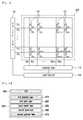
- Fig. 1is a schematic view of a configuration of the capacitance touch sensor panel 100 and the operation thereof in accordance with the embodiment of the present invention.
- the touch sensor panel 100may include a plurality of drive electrodes TX1 to TXn and a plurality of receiving electrodes RX1 to RXm, and may include a drive unit 120 which applies a drive signal to the plurality of drive electrodes TX1 to TXn for the purpose of the operation of the touch sensor panel 100, and a sensing unit 110 which detects the touch and the touch position by receiving a sensing signal including information on the capacitance change amount changing according to the touch on the touch surface of the touch sensor panel 100.
- the touch sensor panel 100may include the plurality of drive electrodes TX1 to TXn and the plurality of receiving electrodes RX1 to RXm. While Fig. 1 shows that the plurality of drive electrodes TX1 to TXn and the plurality of receiving electrodes RX1 to RXm of the touch sensor panel 100 form an orthogonal array, the present invention is not limited to this.
- the plurality of drive electrodes TX1 to TXn and the plurality of receiving electrodes RX1 to RXmhas an array of arbitrary dimension, for example, a diagonal array, a concentric array, a 3-dimensional random array, etc., and an array obtained by the application of them.
- “n” and “m”are positive integers and may be the same as each other or may have different values. The magnitude of the value may be changed depending on the embodiment.
- the plurality of drive electrodes TX1 to TXn and the plurality of receiving electrodes RX1 to RXmmay be arranged to cross each other.
- the drive electrode TXmay include the plurality of drive electrodes TX1 to TXn extending in a first axial direction.
- the receiving electrode RXmay include the plurality of receiving electrodes RX1 to RXm extending in a second axial direction crossing the first axial direction.
- the plurality of drive electrodes TX1 to TXn and the plurality of receiving electrodes RX1 to RXmmay be formed in the same layer.
- the plurality of drive electrodes TX1 to TXn and the plurality of receiving electrodes RX1 to RXmmay be formed on the same side of an insulation layer (not shown).
- the plurality of drive electrodes TX1 to TXn and the plurality of receiving electrodes RX1 to RXmmay be formed in the different layers.
- the plurality of drive electrodes TX1 to TXn and the plurality of receiving electrodes RX1 to RXmmay be formed on both sides of one insulation layer (not shown) respectively, or the plurality of drive electrodes TX1 to TXn may be formed on a side of a first insulation layer (not shown) and the plurality of receiving electrodes RX1 to RXm may be formed on a side of a second insulation layer (not shown) different from the first insulation layer.
- the plurality of drive electrodes TX1 to TXn and the plurality of receiving electrodes RX1 to RXmmay be made of a transparent conductive material (for example, indium tin oxide (ITO) or antimony tin oxide (ATO) which is made of tin oxide (SnO 2 ), and indium oxide (In 2 O 3 ), etc.), or the like.
- ITOindium tin oxide
- ATOantimony tin oxide
- the drive electrode TX and the receiving electrode RXmay be also made of another transparent conductive material or an opaque conductive material.
- the drive electrode TX and the receiving electrode RXmay be formed to include at least any one of silver ink, copper and carbon nanotube (CNT).
- the drive electrode TX and the receiving electrode RXmay be made of metal mesh or nano silver.
- the drive unit 120may apply a drive signal to the drive electrodes TX1 to TXn.
- one drive signalmay be sequentially applied at a time to the first drive electrode TX1 to the n-th drive electrode TXn.
- the drive signalmay be applied again repeatedly. This is just an example.
- the drive signalmay be applied to the plurality of drive electrodes at the same time in accordance with the embodiment.
- the sensing unit 110receives the sensing signal including information on a capacitance (Cm) 101 generated between the receiving electrodes RX1 to RXm and the drive electrodes TX1 to TXn to which the drive signal has been applied, thereby detecting whether or not the touch has occurred and where the touch has occurred.
- the sensing signalmay be a signal coupled by the capacitance (Cm) 101 generated between the receiving electrode RX and the drive electrode TX to which the drive signal has been applied.
- the process of sensing the drive signal applied from the first drive electrode TX1 to the n-th drive electrode TXn through the receiving electrodes RX1 to RXmcan be referred to as a process of scanning the touch sensor panel 100.
- the sensing unit 110may include a receiver (not shown) which is connected to each of the receiving electrodes RX1 to RXm through a switch.
- the switchbecomes the on-state in a time interval during which the signal of the corresponding receiving electrode RX is sensed, thereby allowing the receiver to sense the sensing signal from the receiving electrode RX.
- the receivermay include an amplifier (not shown) and a feedback capacitor coupled between the negative (-) input terminal of the amplifier and the output terminal of the amplifier, i.e., coupled to a feedback path.
- the positive (+) input terminal of the amplifiermay be connected to the ground.
- the receivermay further include a reset switch which is connected in parallel with the feedback capacitor. The reset switch may reset the conversion from current to voltage that is performed by the receiver.
- the negative input terminal of the amplifieris connected to the corresponding receiving electrode RX and receives and integrates a current signal including information on the capacitance (Cm) 101, and then converts the integrated current signal into voltage.
- the sensing unit 110may further include an analog to digital converter (ADC) (not shown) which converts the integrated data by the receiver into digital data. Later, the digital data may be input to a processor (not shown) and processed to obtain information on the touch on the touch sensor panel 100.
- ADCanalog to digital converter
- the sensing unit 110may include the ADC and processor as well as the receiver.
- a controller 130may perform a function of controlling the operations of the drive unit 120 and the sensing unit 110. For example, the controller 130 generates and transmits a drive control signal to the drive unit 120, so that the drive signal can be applied to a predetermined drive electrode TX1 at a predetermined time. Also, the controller 130 generates and transmits the drive control signal to the sensing unit 110, so that the sensing unit 110 may receive the sensing signal from the predetermined receiving electrode RX at a predetermined time and perform a predetermined function.
- the drive unit 120 and the sensing unit 110may constitute a touch detection device (not shown) capable of detecting whether the touch has occurred on the touch sensor panel 100 according to the embodiment of the present invention or not and where the touch has occurred.
- the touch detection device according to the embodiment of the present inventionmay further include the controller 130.
- the touch detection device according to the embodiment of the present inventionmay be integrated and implemented on a touch sensing integrated circuit (IC, see reference numeral 150 of Figs. 10a to 10c ) in a touch input device 1000 including the touch sensor panel 100.
- ICtouch sensing integrated circuit
- the drive electrode TX and the receiving electrode RX included in the touch sensor panel 100may be connected to the drive unit 120 and the sensing unit 110 included in the touch sensing IC 150 through, for example, a conductive trace and/or a conductive pattern printed on a circuit board, or the like.
- the touch sensing IC 150may be located on a circuit board on which the conductive pattern has been printed, for example, a first printed circuit board (hereafter, referred to as a first PCB) indicated by a reference numeral 160 of Fig. 10 .
- the touch sensing IC 150may be mounted on a main board for operation of the touch input device 1000.
- a capacitance (Cm) with a predetermined valueis generated at each crossing of the drive electrode TX and the receiving electrode RX.
- the value of the capacitancemay be changed.
- the capacitancemay represent a mutual capacitance (Cm).
- the sensing unit 110senses such electrical characteristics, thereby being able to sense whether the touch has occurred on the touch sensor panel 100 or not and where the touch has occurred.
- the sensing unit 110is able to sense whether the touch has occurred on the surface of the touch sensor panel 100 comprised of a two-dimensional plane consisting of a first axis and a second axis.
- the drive electrode TX to which the drive signal has been appliedis detected, so that the position of the second axial direction of the touch can be detected.
- the capacitance changeis detected from the reception signal received through the receiving electrode RX, so that the position of the first axial direction of the touch can be detected.
- the touch sensor panel 100 for detecting whether or not the touch has occurred and where the touch has occurredmay be implemented by using not only the above-described method but also any touch sensing method like a self-capacitance type method, a surface capacitance type method, a projected capacitance type method, a resistance film method, a surface acoustic wave (SAW) method, an infrared method, an optical imaging method, a dispersive signal technology, and an acoustic pulse recognition method, etc.
- a self-capacitance type methoda surface capacitance type method
- a projected capacitance type methoda resistance film method
- SAWsurface acoustic wave
- the touch sensor panel 100 for detecting where the touch has occurred in the touch input device 1000may be positioned outside or inside a display module 200.
- the display module 200 of the touch input device 1000may be a display panel included in a liquid crystal display (LCD), a plasma display panel (PDP), an organic light emitting diode (OLED), etc. Accordingly, a user may perform the input operation by touching the touch surface while visually identifying an image displayed on the display panel.
- the display module 200may include a control circuit which receives an input from an application processor (AP) or a central processing unit (CPU) on a main board for the operation of the touch input device 1000 and displays the contents that the user wants on the display panel.
- the control circuitmay be mounted on a second printed circuit board (hereafter, referred to as a second PCB) (210) in Figs. 9a to 10c .
- the control circuit for the operation of the display module 200may include a display panel control IC, a graphic controller IC, and a circuit required to operate other display panels 200.
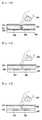
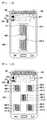
- Figs. 2a , 2b and 2care conceptual views showing a relative position of the touch sensor panel with respect to the display module in the touch input device according to the embodiment of the present invention. While Figs. 2a to 2c show an LCD panel as a display panel 200A included within the display module 200, this is just an example. Any display panel may be applied to the touch input device 1000 according to the embodiment of the present invention.
- the reference numeral 200Amay designate the display panel included in the display module 200.
- the LCD panel 200Amay include a liquid crystal layer 250 including a liquid crystal cell, a first glass layer 261 and a second glass layer 262 which are disposed on both sides of the liquid crystal layer 250 and include electrodes, a first polarizer layer 271 formed on a side of the first glass layer 261 in a direction facing the liquid crystal layer 250, and a second polarizer layer 272 formed on a side of the second glass layer 262 in the direction facing the liquid crystal layer 250.
- the LCD panelmay further include other configurations for the purpose of performing the displaying function and may be transformed.
- Fig. 2ashows that the touch sensor panel 100 of the touch input device 1000 is disposed outside the display module 200.
- the touch surface of the touch input device 1000may be the surface of the touch sensor panel 100.
- the top surface of the touch sensor panel 100is able to function as the touch surface.
- the touch surface of the touch input device 1000may be the outer surface of the display module 200.
- the bottom surface of the second polarizer layer 272 of the display module 200is able to function as the touch surface.
- the bottom surface of the display module 200may be covered with a cover layer (not shown) like glass.
- Figs. 2b and 2cshow that the touch sensor panel 100 of the touch input device 1000 is disposed inside the display panel 200A.
- the touch sensor panel 100 for detecting the touch positionis disposed between the first glass layer 261 and the first polarizer layer 271.
- the touch surface of the touch input device 1000is the outer surface of the display module 200.
- the top surface or bottom surface of the display module 200 in Fig. 2bmay be the touch surface.
- Fig. 2cshows that the touch sensor panel 100 for detecting the touch position is included in the liquid crystal layer 250.
- the touch surface of the touch input device 1000is the outer surface of the display module 200.
- the top surface or bottom surface of the display module 200 in Fig. 2cmay be the touch surface.
- the top surface or bottom surface of the display module 200which can be the touch surface, may be covered with a cover layer (not shown) like glass.
- Fig. 3is a cross sectional view of the touch input device configured to detect the touch position and touch pressure in accordance with a first embodiment of the present invention.
- the touch sensor panel 100 and the pressure detection module 400 which detect the touch positionmay be attached on the front side of the display module 200, As a result, the display screen of the display module 200 can be protected and the touch detection sensitivity of the touch sensor panel 100 can be improved.
- the pressure detection module 400may be operated apart from the touch sensor panel 100 which detects the touch position.
- the pressure detection module 400may be configured to detect only the touch pressure independently of the touch sensor panel 100 which detects the touch position.
- the pressure detection module 400may be configured to be coupled to the touch sensor panel 100 which detects the touch position and to detect the touch pressure.
- at least one of the drive electrode TX and the receiving electrode RX included in the touch sensor panel 100 which detects the touch positionmay be used to detect the touch pressure.
- Fig. 3shows that the pressure detection module 400 is coupled to the touch sensor panel 100 and detects the touch pressure.
- the pressure detection module 400includes a spacer layer 420 which leaves a space between the touch sensor panel 100 and the display module 200.
- the pressure detection module 400may include a reference potential layer spaced from the touch sensor panel 100 by the spacer layer 420.
- the display module 200may function as the reference potential layer.
- the reference potential layermay have any potential which causes the change of the capacitance 101 generated between the drive electrode TX and the receiving electrode RX.
- the reference potential layermay be a ground layer having a ground potential.
- the reference potential layermay be the ground layer of the display module 200.
- the reference potential layermay have a parallel plane with the two-dimensional plane of the display module 200.
- the touch sensor panel 100is disposed apart from the display module 200, i.e., the reference potential layer.
- the spacer layer 420may be implemented in the form of an air gap between the touch sensor panel 100 and the display module 200.
- the spacer layer 420may be made of an impact absorbing material in accordance with the embodiment.
- the spacer layer 420may be filled with a dielectric material in accordance with the embodiment.
- a double adhesive tape (DAT) 430may be used to fix the touch sensor panel 100 and the display module 200.
- DATdouble adhesive tape
- the areas the touch sensor panel 100 and the display module 200are overlapped with each other.
- the touch sensor panel 100 and the display module 200are adhered to each other by adhering the edge portions of the touch sensor panel 100 and the display module 200 through use of the DAT 430.
- the rest portions of the touch sensor panel 100 and the display module 200may be spaced apart from each other by a predetermined distance " d ".
- the capacitance (Cm) 101 between the drive electrode TX and the receiving electrode RXis changed. That is, when the touch occurs on the touch sensor panel 100, the mutual capacitance (Cm) 101 may become smaller than a base mutual capacitance. This is because, when the conductive object like a finger approaches close to the touch sensor panel 100, the object functions as the ground GND, and then a fringing capacitance of the mutual capacitance (Cm) 101 is absorbed in the object.
- the base mutual capacitanceis the value of the mutual capacitance between the drive electrode TX and the receiving electrode RX when there is no touch on the touch sensor panel 100.
- the touch sensor panel 100When the object touches the top surface, i.e., the touch surface of the touch sensor panel 100 and a pressure is applied to the top surface, the touch sensor panel 100 may be bent. Here, the value of the mutual capacitance (Cm) 101 between the drive electrode TX and the receiving electrode RX may be more reduced. This is because the bend of the touch sensor panel 100 causes the distance between the touch sensor panel 100 and the reference potential layer to be reduced from “ d " to " d' ", so that the fringing capacitance of the mutual capacitance (Cm) 101 is absorbed in the reference potential layer as well as in the object. When a nonconductive object touches, the change of the mutual capacitance (Cm) 101 is simply caused by only the change of the distance " d-d' " between the touch sensor panel 100 and the reference potential layer.
- the touch input device 1000is configured to include the touch sensor panel 100 and the pressure detection module 400 on the display module 200, so that not only the touch position but also the touch pressure can be simultaneously detected.
- the pressure detection module 400 as well as the touch sensor panel 100is disposed on the display module 200, the display properties of the display module is deteriorated. Particularly, when the air gap is included on the display module 200, the visibility and optical transmittance of the display module may be lowered.
- the air gapis not disposed between the display module 200 and the touch sensor panel 100 for detecting the touch position.
- the touch sensor panel 100 and the display module 200can be completely laminated by means of an adhesive like an optically clear adhesive (OCA).
- OCAoptically clear adhesive
- Fig. 4ais a cross sectional view of the touch input device according to a second embodiment of the present invention.
- the complete laminationis made by an adhesive between the touch sensor panel 100 and the display module 200 for detecting the touch position.
- the display color clarity, visibility and optical transmittance of the display module 200which can be recognized through the touch surface of the touch sensor panel 100, can be improved.
- the touch input device 1000As the touch input device 1000 according to the second embodiment of the present invention, the touch sensor panel 100 is laminated and attached on the display module 200 by means of an adhesive.
- the touch input device 1000 according to the second embodiment of the present inventionmay include, as shown in Figs. 2b and 2c , that the touch sensor panel 100 is disposed inside the display module 200. More specifically, while Figs. 4a , 4b and 5 show that the touch sensor panel 100 covers the display module 200, the touch input device 1000 which includes the touch sensor panel 100 disposed inside the display module 200 and includes the display module 200 covered with a cover layer like glass may be used as the second embodiment of the present invention.
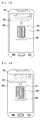
- the touch input device 1000may include an electronic device including the touch screen, for example, a cell phone, a personal data assistant (PDA), a smart phone, a tablet personal computer, an MP3 player, a laptop computer, etc.
- PDApersonal data assistant
- a smart phonefor example, a cell phone, a personal data assistant (PDA), a smart phone, a tablet personal computer, an MP3 player, a laptop computer, etc.
- a substrate 300together with an outermost cover 320 of the touch input device 1000, functions as, for example, a housing which surrounds a mounting space 310, etc., where the circuit board and/or battery for operation of the touch input device 1000 are placed.
- the circuit board for operation of the touch input device 1000may be a main board.
- a central processing unit (CPU), an application processor (AP) or the likemay be mounted on the circuit board. Due to the substrate 300, the display module 200 is separated from the circuit board and/or battery for operation of the touch input device 1000. Due to the substrate 300, electrical noise generated from the display module 200 can be blocked.
- the touch sensor panel 100 or front cover layer of the touch input device 1000may be formed wider than the display module 200, the substrate 300, and the mounting space 310.
- the cover 320is formed such that the cover 320, together with the touch sensor panel 100, surrounds the display module 200, the substrate 300, and the circuit board.
- the touch input device 1000may detect the touch position through the touch sensor panel 100 and may detect the touch pressure by disposing the electrodes 450 and 460 for detecting a pressure between the display module 200 and the substrate 300.
- the touch sensor panel 100may be disposed inside or outside the display module 200.
- the touch pressurecan be detected by using the air gap and/or potential layer which are positioned inside or outside the display module 200 without manufacturing a separate spacer layer and/or reference potential layer. This will be described in detail with reference to Figs. 4b to 7b .
- Fig. 4bis an exemplary cross sectional view of the display module 200 which can be included in the touch input device 1000 according to the second embodiment of the present invention.
- Fig. 4bshows an LCD module as the display module 200.
- the LCD module 200may include an LCD panel 200A and a backlight unit 200B.
- the LCD panel 200Acannot emit light in itself but simply performs a function to block or transmit the light. Therefore, a light source is positioned in the lower portion of the LCD panel 200A and light is illuminated onto the LCD panel 200A, so that a screen displays not only brightness and darkness but information with various colors. Since the LCD panel 200A is a passive device and cannot emit the light in itself, a light source having a uniform luminance distribution is required on the rear side.
- the structures and functions of the LCD panel 200A and the backlight unit 200Bhave been already known to the public and will be briefly described below.
- the backlight unit 200B for the LCD panel 200Amay include several optical parts.
- the backlight unit 200Bmay include a light diffusing and light enhancing sheet 231, a light guide plate 232, and a reflection plate 240.
- the backlight unit 200Bmay include a light source (not shown) which is formed in the form of a linear light source or point light source and is disposed on the rear and/or side of the light guide plate 232.
- a support 233may be further included on the edges of the light guide plate 232 and the light diffusing and light enhancing sheet 231.
- the light guide plate 232may generally convert lights from the light source (not shown) in the form of a linear light source or point light source into light from a light source in the form of a surface light source, and allow the light to proceed to the LCD panel 200A.
- a part of the light emitted from the light guide plate 232may be emitted to a side opposite to the LCD panel 200A and be lost.
- the reflection plate 240may be positioned below the light guide plate 232 so as to cause the lost light to be incident again on the light guide plate 232, and may be made of a material having a high reflectance.
- the light diffusing and light enhancing sheet 231may include a diffuser sheet and/or a prism sheet.
- the diffuser sheetfunctions to diffuse the light incident from the light guide plate 232. For example, light scattered by the pattern of the light guide plate 232 comes directly into the eyes of the user, and thus, the pattern of the light guide plate 232 may be shown as it is. Moreover, since such a pattern can be clearly sensed even after the LCD panel 200A is mounted, the diffuser sheet is able to perform a function to offset the pattern of the light guide plate 232.
- the prism sheetmay be included in order to improve the luminance of the light by focusing the light again.
- the backlight unit 200Bmay include a configuration different from the above-described configuration in accordance with the technical change and development and/or the embodiment.
- the backlight unit 200Bmay further include an additional configuration as well as the foregoing configuration.
- the backlight unit 200B according to the embodiment of the presentmay further include, for example, a protection sheet on the prism sheet.
- the backlight unit 200Bmay also further include a lamp cover in accordance with the embodiment so as to minimize the optical loss of the light source.
- the backlight unit 200Bmay also further include a frame which maintains a shape enabling the light diffusing and light enhancing sheet 231, the light guide plate 232, a lamp (not shown), and the like, which are main components of the backlight unit 200B, to be exactly combined together in accordance with an allowed dimension.
- the each of the componentsmay be comprised of at least two separate parts.
- the prism sheetmay include two prism sheets.
- a first air gap 220-2may be positioned between the light guide plate 232 and the reflection plate 240.
- the lost light from the light guide plate 232 to the reflection plate 240can be incident again on the light guide plate 232 by the reflection plate 240.
- a double adhesive tape 221-2may be included on the edges of the light guide plate 232 and the reflection plate 240.
- the backlight unit 200B and the LCD panel 200Amay be positioned with a second air gap 220-1 placed therebetween. This intends to prevent that the impact from the LCD panel 200A is transmitted to the backlight unit 200B.
- a double adhesive tape 221-1may be included on the edges of the LCD panel 200A and the backlight unit 200B.
- the display module 200may be configured to include in itself the air gap such as the first air gap 220-2 and/or the second air gap 220-1. Also, the air gap may be included between a plurality of the layers of the light diffusing and light enhancing sheet 231. In the foregoing, while the LCD module has been described, the air gap may be included within the structure of another display module.
- the touch input device 1000may make use of the air gap which has been already positioned inside or outside the display module 200 without manufacturing a separate spacer layer.
- the air gap which is used as the spacer layermay be not only the first air gap 220-2 and/or the second air gap 220-1 which are described with reference to Fig. 4b but also any air gap included inside the display module 200.
- the air gap which is used as the spacer layermay be an air gap included outside the display module 200.
- Fig. 5is a perspective view of the touch input device according to the second embodiment of the present invention.
- the touch input device 1000may include electrodes 450 and 460 which are disposed between the display module 200 and the substrate 200 and detect the pressure.
- the electrodes 450 and 460 for detecting the pressureare designated as pressure electrodes 450 and 460.
- the pressure electrodes 450 and 460may be made of an opaque material as well as a transparent material.
- FIG. 6ais a cross sectional view of the touch input device including the pressure electrode pattern according to the first embodiment of the present invention.
- the pressure electrodes 450 and 460 according to the first embodiment of the present inventionmay be formed on the substrate 300.
- the pressure electrodes 450 and 460are shown exaggeratedly thick for convenience of description. However, since the pressure electrodes 450 and 460 can be implemented in the form of a sheet, the thickness of the first electrode 450 and the second electrode 460 may be very small.
- Figs. 6a and 6bshow that the display module 200 and the pressure electrodes 450 and 460 are spaced apart from each other so as to represent that the first electrode 450 and the second electrode 460 have been formed on the substrate 300. However, this is for description only. The display module 200 and the first and second electrodes 450 and 460 may not be spaced apart from each other.
- the pressure electrode for detecting the pressuremay include the first electrode 450 and the second electrode 460.
- any one of the first and the second electrodes 450 and 460may be a drive electrode and the other may be a receiving electrode.
- a drive signalis applied to the drive electrode, and a sensing signal may be obtained through the receiving electrode.
- the mutual capacitancemay be generated between the first electrode 450 and the second electrode 460.
- Fig. 6ashows that the display module 200 includes a spacer layer 220 and a reference potential layer 270.
- the spacer layer 220may be, as described with reference to Fig. 4b , the first air gap 220-2 and/or the second air gap 220-1 which are included during the manufacture of the display module 200.
- the air gapmay function as the spacer layer 220.
- the display module 220includes a plurality of air gaps, the plurality of air gaps may collectively function as the spacer layer 220.
- Figs. 6a to 6c and Fig. 7ashow that the display module 200 functionally includes one spacer layer 220.
- the touch input device 1000may include the reference potential layer 270 which is positioned above the spacer layer 220 within the display module 200 of Figs. 2a to 2c .
- the reference potential layer 270may be a ground potential layer which is included in itself during the manufacture of the display module 200.
- an electrode (not shown) for blocking the noisemay be included between the first polarizer layer 271 and the first glass layer 261.
- the electrode for blocking the noisemay be composed of ITO and may function as the ground.
- the reference potential layer 270may be located at any position causing the spacer layer 220 to be placed between the reference potential layer 270 and the pressure electrodes 450 and 460. Not only the above-described blocking electrode but also an electrode having any potential may be used as the reference potential layer 270.
- the reference potential layer 270may be a common electrode potential (Vcom) layer of the display module 200.
- the display module 200may not be surrounded by a separate cover or frame.
- the bottom surface of the display module 200which faces the substrate 300, may be the reflection plate 240 and/or a nonconductor.
- the bottom surface of the display module 200cannot have the ground potential.
- it is possible to detect the touch pressureby using any potential layer positioned within the display module 200 as the reference potential layer 270 through use of the touch input device 1000 according to the embodiment of the present invention.
- Fig. 6bis a cross sectional view of a case where a pressure has been applied to the touch input device 1000 shown in Fig. 6a .
- the touch sensor panel 100 or the display module 200may be bent or pressed.
- the distance " d " between the reference potential layer 270 and the pattern of the pressure electrodes 450 and 460may be decreased to " d' " by the spacer layer 220 positioned within the display module 200.
- the fringing capacitanceis absorbed in the reference potential layer 270, so that the mutual capacitance between the first electrode 450 and the second electrode 460 may be reduced. Therefore, the magnitude of the touch pressure can be calculated by obtaining the reduction amount of the mutual capacitance from the sensing signal obtained through the receiving electrode.
- a statemay be created in which the distance between the reference potential layer 270 and the pattern of the pressure electrodes 450 and 460 is not reduced any more at a predetermined position.
- this statewill be referred to as a saturation state.
- an area in the saturation statewhere the distance between the reference potential layer 270 and the pattern of the pressure electrodes 450 and 460 is not reduced any more may become greater.
- the magnitude of the touch pressureis calculated by the change of the capacitance according to the distance change. However, this may include that the magnitude of the touch pressure is calculated by the change of the area in the saturation state.
- the display module 200may be bent or pressed by the touch pressure.
- the display module 200may be bent or pressed in such a manner as to show the biggest transformation at the touch position.
- a position showing the biggest transformationmay not match the touch position.
- the display module 200may be shown to be bent or pressed at least at the touch position.
- the touch positionapproaches close to the border, edge, etc., of the display module 200
- the most bent or pressed position of the display module 200may not match the touch position, however, the display module 200 may be shown to be bent or pressed at least at the touch position.
- the layer positioned below the spacer layer 220e.g., the reflection plate
- the layer positioned below the spacer layer 220may not be bent or pressed or may be less bent or pressed due to the spacer layer 220.
- Fig. 6bshows that the lowest portion of the display module 200 is not bent or pressed at all, this is just an example.
- the lowest portion of the display module 200may be bent or pressed.
- the degree to which the lowest portion of the display module 200 is bent or pressedcan be reduced by the spacer layer 220.
- the top surface of the substrate 300may also have the ground potential in order to block the noise. Therefore, in order to prevent a short-circuit from occurring between the substrate 300 and the pressure electrodes 450 and 460, the pressure electrodes 450 and 460 may be formed on an insulation layer 470.
- Fig. 8shows an attachment structure of the pressure electrode according the embodiment of the present invention. Referring to (a) of Fig. 8 , the first insulation layer 470 is positioned on the substrate 300, and then the pressure electrodes 450 and 460 are formed. Also, according to the embodiment, the first insulation layer 470 on which the pressure electrodes 450 and 460 have been formed may be attached on the substrate 300. Also, the pressure electrode according to the embodiment may be formed by positioning a mask, which has a through-hole corresponding to the pressure electrode pattern, on the substrate 300 or on the first insulation layer 470 positioned on the substrate 300, and then by spraying a conductive material.
- the pressure electrodes 450 and 460may be covered with an additional second insulation layer 471 in order to prevent a short-circuit from occurring between the display module 200 and the pressure electrodes 450 and 460 positioned on the substrate 300. Also, the pressure electrodes 450 and 460 formed on the first insulation layer 470 are covered with the additional second insulation layer 471 and then are integrally attached on the substrate 300, so that the pressure detection module 400 is formed.
- the pressure electrodes 450 and 460 attachment structure and methodwhich have been described with reference to (a) of Fig. 8 , may be applied to the attachment of the pressure electrodes 450 and 460 to the display module 200.
- the attachment of the pressure electrodes 450 and 460 to the display module 200will be described in more detail with reference to Fig. 6e .
- the substrate 300 or the display module 200 on which the pressure electrodes 450 and 460 are attachedmay not have the ground potential or may have a weak ground potential.
- the touch input device 1000 according to the embodiment of the presentmay further include a ground electrode (not shown) between the first insulation layer 470 and either the substrate 300 or the display module 200.
- another insulation layer(not shown) may be included between the ground electrode and either the substrate 300 or the display module 200.
- the ground electrode(not shown) is able to prevent the size of the capacitance generated between the first electrode 450 and the second electrode 460, which are pressure electrodes, from increasing excessively.
- Fig. 6cis a cross sectional view of the touch input device including the pressure electrode pattern according to a modified example of the first embodiment of the present invention.
- Fig. 6cshows that the spacer layer 220 is positioned between the display module 200 and the substrate 300.
- the touch input device 1000 including the display module 200is manufactured, the display module 200 is not completely attached to the substrate 300, so that the air gap 420 may be created.
- the air gap 420as the spacer layer for detecting the touch pressure, it is possible to reduce the time and cost intentionally required for manufacturing the spacer layer for detecting the touch pressure.
- Figs. 6c and 6dshow that the air gap 220 used as the spacer layer is not positioned within the display module 200. However, Figs. 6c and 6d may additionally include a case where the air gap 220 is positioned within the display module 200.
- Fig. 6dis a cross sectional view of a case where a pressure has been applied to the touch input device shown in Fig. 6c .
- the display module 200may be bent or pressed.
- the " d " between the reference potential layer 270 and the pattern of the pressure electrodes 450 and 460may be decreased to " d' " by the spacer layer which are positioned between the reference potential layer 270 and the pressure electrodes 450 and 460.
- a fringing capacitanceis absorbed into the reference potential layer 270 due to the decrease of the distance " d ", so that the mutual capacitance between the first electrode 450 and the second electrode 460 may be reduced.
- the magnitude of the touch pressurecan be calculated by obtaining the reduction amount of the mutual capacitance from the sensing signal obtained through the receiving electrode.
- Fig. 6eis a cross sectional view of the touch input device including a pressure electrode pattern according to the second embodiment of the present invention. While the first embodiment shows that the pressure electrodes 450 and 460 are formed on the substrate 300, the pressure electrodes 450 and 460 can be formed on the bottom surface of the display module 200. The distance " d " between the reference potential layer 270 and the pressure electrodes 450 and 460 is reduced by touching the touch surface of the touch sensor panel 100. Consequently, this may cause the change of the mutual capacitance between the first electrode 450 and the second electrode 460.
- Fig. 6eshows that the substrate 300 and the pressure electrodes 450 and 460 are spaced apart from each other so as to describe that the pressure electrodes 450 and 460 are attached on the display module 200.
- the substrate 300 and the pressure electrodes 450 and 460may not be spaced apart from each other. Also, as with Figs. 6c and 6d , the display module 200 and the substrate 300 may be spaced apart from each other by the air gap 420.
- Fig. 6fshows a pattern of the pressure electrode according to the first embodiment of the present invention.
- Fig. 6dshows that the first electrode 450 and the second electrode 460 are formed on the substrate 300.
- the capacitance between the first electrode 450 and the second electrode 460may be changed depending on the distance between the reference potential layer 270 and the pressure electrodes 450 and 460.
- Fig. 6gshows a pattern of the pressure electrode according to the second embodiment of the present invention.
- Fig. 6gshows that the pattern of the pressure electrodes 450 and 460 have been formed on the bottom surface of the display module 200.
- Figs. 6h and 6ishow patterns of the pressure electrodes 450 and 460 which can be applied to the embodiment of the present invention.
- the magnitude of the touch pressureis detected as the mutual capacitance between the first electrode 450 and the second electrode 460 is changed, it is necessary to form the patterns of the first electrode 450 and the second electrode 460 so as to generate the range of the capacitance required to improve the detection accuracy.
- the patterncan be designed by adjusting the size of the facing area, facing length and facing shape of the first electrode 450 and the second electrode 460 in accordance with the range of the necessary capacitance.
- Figs. 6h and 6ishow that the first electrode 450 and the second electrode 460 are formed in the same layer, and show that the pressure electrode is formed such that the facing length of the first electrode 450 and the second electrode 460 becomes relatively longer.
- the first and second embodimentsshow that the first electrode 450 and the second electrode 460 are formed in the same layer. However, it can be considered that the first electrode 450 and the second electrode 460 are formed in different layers in accordance with the embodiment. It is shown in (b) of Fig. 8 that an attachment structure in which the first electrode 450 and the second electrode 460 are formed in different layers. As shown in (b) of Fig.8 , the first electrode 450 may be formed on the first insulation layer 470, and the second electrode 460 may be formed on the second insulation layer 471 positioned on the first electrode 450. According to the embodiment, the second electrode 460 may be covered with a third insulation layer 472.
- first electrode 450 and the second electrode 460are disposed in different layers, they can be implemented so as to overlap each other.
- the first electrode 450 and the second electrode 460may be formed similarly to the pattern of the drive electrode TX and receiving electrode RX which are arranged in the form of M ⁇ N array and are included in the touch sensor panel 100 described with reference to Fig. 1 .
- M and Nmay be natural numbers greater than 1.
- the first embodimentshows that the touch pressure is detected from the change of the mutual capacitance between the first electrode 450 and the second electrode 460.
- the pressure electrodes 450 and 460may be configured to include only any one of the first electrode 450 and the second electrode 460. In this case, it is possible to detect the magnitude of the touch pressure by detecting the change of the capacitance between the one pressure electrode and the reference potential layer 270.
- the pressure electrodemay be configured to include only the first electrode 450.
- the magnitude of the touch pressurecan be detected by the change of the capacitance between the first electrode 450 and the reference potential layer 270, which is caused by the distance change between the reference potential layer 270 and the first electrode 450. Since the distance " d " is reduced with the increase of the touch pressure, the capacitance between the reference potential layer 270 and the first electrode 450 may be increased with the increase of the touch pressure.
- the pressure electrodeshould not necessary have a comb teeth shape or a trident shape, which is required to improve the detection accuracy of the mutual capacitance change amount.
- the pressure electrodemay have a plate shape (e.g., quadrangular plate).
- an attachment structure in which the pressure electrode is formed to include only the first electrode 450may include only the first electrode 450.
- the first electrode 450may be formed on the first insulation layer 470 positioned on the substrate 300 or display module 200. Also, according to the embodiment, the first electrode 450 may be covered with the second insulation layer 471.
- Fig. 7ais a cross sectional view of the touch input device including the pressure electrode pattern according to a third embodiment of the present invention.
- the pressure electrodes 450 and 460 according to the third embodimentmay be formed on the top surface of the substrate 300 and on the bottom surface of the display module 200.
- the pressure electrode pattern for detecting the pressuremay include the first electrode 450 and the second electrode 460.
- any one of the first electrode 450 and the second electrode 460may be formed on the substrate 300, and the other may be formed on the bottom surface of the display module 200.
- Fig. 7ashows that the first electrode 450 is formed on the substrate 300, and the second electrode 460 is formed on the bottom surface of the display module 200.
- Fig. 7ashows that the first electrode 450 is spaced apart from the second electrode 460.
- thisis just intended to describe that the first electrode 450 is formed on the substrate 300 and the second electrode 460 is formed on the display module 200.
- the first electrode 450 and the second electrode 460may be spaced apart from each other by the air gap, may have an insulating material placed therebetween, or may be formed to deviate from each other, for example, may be formed in the same layer, not to be overlapped with each other.
- the touch sensor panel 100 and the display module 200may be bent or pressed.
- the distance " d " between the reference potential layer 270 and the first and second electrodes 450 and 460may be reduced.
- the mutual capacitance between the first electrode 450 and the second electrode 460may be decreased with the reduction of the distance " d ". Therefore, the magnitude of the touch pressure can be calculated by obtaining the decrease amount of the mutual capacitance from the sensing signal obtained through the receiving electrode.
- Fig. 7bshows a pattern of the pressure electrode according to the third embodiment of the present invention.
- Fig. 7bshows that the first electrode 450 is formed on the bottom surface of the display module 200 and the second electrode 460 is formed on the top surface of the substrate 300.
- the first electrode 450 and the second electrode 460are disposed perpendicular to each other, so that the capacitance change amount detection sensitivity can be enhanced.
- the first electrode 450may be positioned on the first insulation layer 470-2 formed on the substrate 300 and may be covered with the second insulation layer 471-2.
- the second electrode 460may be positioned on the first insulation layer 470-1 formed on the bottom surface of the display module 200 and may be covered with the second insulation layer 471-1.
- a ground electrodemay be further included between the first insulation layers 470, 470-1, and 470-2 in (a) to (d) of Fig. 8 .
- an additional insulation layermay be further included between the ground electrode (not shown) and either the substrate 300 or the display module 200 on which the pressure electrodes 450 and 460 are attached.
- the touch input device 1000senses the capacitance change occurring in the pressure electrodes 450 and 460. Therefore, it is necessary for the drive signal to be applied to the drive electrode out of the first and second electrodes 450 and 460, and it is required to detect the touch pressure by the capacitance change amount by obtaining the sensing signal from the receiving electrode. According to the embodiment, it is possible to additionally include the touch sensing IC for the operation of the detection pressure. In this case, the touch input device repeatedly has a configuration similar to the configuration of Fig. 1 including the drive unit 120, sensing unit 110, and controller 130, so that the area and volume of the touch input device 1000 increase.
- the touch input device 1000applies the drive signal for the operation of the touch sensor panel 100 through the touch detection device and receives the sensing signal, so that the touch pressure can be detected.
- the first electrode 450is the drive electrode and the second electrode 460 is the receiving electrode.
- the drive signalmay be applied to the first electrode 450 from the drive unit 120, and the second electrode 460 may transmit the sensing signal to the sensing unit 110.
- the controller 130may perform the scanning of the touch sensor panel 100, and simultaneously perform the scanning of the touch pressure detection, or the controller 130 performs the time-sharing, and then may generate a control signal such that the scanning of the touch sensor panel 100 is performed in a first time interval and the scanning of the pressure detection is performed in a second time interval different from the first time interval.
- the first electrode 450 and the second electrode 460should be electrically connected to the drive unit 120 and/or the sensing unit 110.
- the touch detection device for the touch sensor panel 100corresponds to the touch sensing IC 150 and is formed on one end of the touch sensor panel 100 or on the same plane with the touch sensor panel 100.
- the pattern of the pressure electrodes 450 and 460may be electrically connected to the touch detection device of the touch sensor panel 100 by any method.
- the pattern of the pressure electrodes 450 and 460may be connected to the touch detection device through a connector by using the second PCB 210 included in the display module 200.
- the conductive traces 451 and 461which electrically extend from the first electrode 450 and the second electrode 460 respectively may be electrically connected to the touch sensing IC 150 through the second PCB 210, etc.
- Figs. 9a and 9bshow an attachment method of the pressure electrode according the second embodiment of the present invention.
- Figs. 9a and 9bshow that the pressure electrodes 450 and 460 according to the embodiment of the present invention are attached to the bottom surface of the display module 200.
- Figs. 9a and 9bshow the second PCB 210 on which a circuit for the operation of the display panel has been mounted is disposed on a portion of the bottom surface of the display module 200.
- Fig. 9ashows that the pattern of the pressure electrodes 450 and 460 are attached to the bottom surface of the display module 200 such that the first electrode 450 and the second electrode 460 are connected to one end of the second PCB 210 of the display module 200.
- Fig. 9ashows that the first electrode 450 and the second electrode 460 are manufactured on the insulation layer 470.
- the pattern of the first electrode 450 and the pattern of the second electrode 460is formed on the insulation layer 470 and may be attached as an integrated formed sheet on the bottom surface of the display module 200.
- a conductive patternmay be printed on the second PCB 210 in such a manner as to electrically connect the pattern of the pressure electrodes 450 and 460 to a necessary component like the touch sensing IC 150, etc.
- the attachment method of the pattern of the pressure electrodes 450 and 460which has been shown in Fig. 9a , can be applied in the same manner to the substrate 300.
- Fig. 9bshows that the pressure electrodes 450 and 460 are integrally formed on the second PCB 210 of the display module 200.
- the second PCB 210 of the display module 200is manufactured, a certain area is separated from the second PCB 210, and then not only the circuit for the operation of the display panel but also the pattern corresponding to the first electrode 450 and the second electrode 460 can be printed on the area.
- a conductive patternmay be printed on the second PCB 210 in such a manner as to electrically connect the first electrode 450 and the second electrode 460 to a necessary component like the touch sensing IC 150, etc.
- Figs 10a to 10cshow how the pressure electrode is connected to the touch sensing IC 150 in accordance with the second embodiment of the present invention.
- the touch sensor panel 100is included outside the display module 200.
- Figs. 10a to 10cshow that the touch detection device of the touch sensor panel 100 is integrated in the touch sensing IC 150 mounted on the first PCB 160 for the touch sensor panel 100.
- Fig. 10ashows that the pressure electrodes 450 and 460 attached to the display module 200 are connected to the touch sensing IC 150 through a first connector 121.
- the touch sensing IC 150is connected to the second PCB 210 for the display module 200 through the first connector 121.
- the second PCB 210may be electrically connected to the main board through a second connector 224. Therefore, through the first connector 121 and the second connector 224, the touch sensing IC 150 may transmit and receive a signal to and from the CPU or AP for the operation of the touch input device 1000.
- FIG. 10ashows that the first electrode 450 is attached to the display module 200 by the method shown in Fig. 9b
- the first electrode 450can be attached to the display module 200 by the method shown in Fig. 9a .
- a conductive patternmay be printed on the second PCB 210 in such a manner as to electrically connect the first electrode 450 and the second electrode 460 to the touch sensing IC 150 through the first connector 121.
- Fig. 10bshows that the pressure electrodes 450 and 460 attached to the display module 200 are connected to the touch sensing IC 150 through a third connector 473.
- the pressure electrodes 450 and 460may be connected to the main board for the operation of the touch input device 1000 through the third connector 473, and in the future, may be connected to the touch sensing IC 150 through the second connector 224 and the first connector 121.
- the pressure electrodes 450 and 460may be printed on the additional PCB 211 separated from the second PCB 210.
- the pattern of the pressure electrodes 450 and 460may be formed on the insulation layer 470 and may be connected to the main board through the third connector 473 by extending the conductive trace, etc., from the pressure electrodes 450 and 460.
- Fig. 10cshows that the pattern of the pressure electrodes 450 and 460 are directly connected to the touch sensing IC 150 through a fourth connector 474.
- the pressure electrodes 450 and 460may be connected to the first PCB 160 through the fourth connector 474.
- a conductive patternmay be printed on the first PCB 160 in such a manner as to electrically connect the fourth connector 474 to the touch sensing IC 150.
- the pressure electrodes 450 and 460may be connected to the touch sensing IC 150 through the fourth connector 474.
- the pressure electrodes 450 and 460may be printed on the additional PCB 211 separated from the second PCB 210.
- the second PCB 210may be insulated from the additional PCB 211 so as not to be short-circuited with each other.
- the pressure electrodes 450 and 460may be formed on the insulation layer 470 and may be connected to the first PCB 160 through the fourth connector 474 by extending the conductive trace, etc., from the pressure electrodes 450 and 460.
- connection method of Figs. 10b and 10ccan be applied to the case where the pressure electrodes 450 and 460 are formed on the substrate 300 as well as on the bottom surface of the display module 200.
- Figs. 10a to 10chave been described by assuming that a chip on board (COB) structure in which the touch sensing IC 150 is formed on the first PCB 160.
- COBchip on board
- the present inventioncan be applied to the chip on board (COB) structure in which the touch sensing IC 150 is mounted on the main board within the mounting space 310 of the touch input device 1000. It will be apparent to those skilled in the art from the descriptions of Figs. 10a to 10c that the connection of the pressure electrodes 450 and 460 through the connector can be also applied to another embodiment.
- the pressure electrodes 450 and 460that is to say, has described that the first electrode 450 constitutes one channel as the drive electrode and the second electrode 460 constitutes one channel as the receiving electrode.
- the drive electrode and the receiving electrodeconstitute a plurality of channels respectively, so that a plurality of pressure detection can be made based on the multi-touch.
- Figs. 11a to 11cshow that the pressure electrode according to the embodiment of the present invention constitutes the plurality of channels.
- Fig. 11ashows the first electrode 450-1 and 450-2 and the second electrode 460-1 and 460-2 constitute two channels respectively.
- Fig. 11bshows that the first electrode 450 constitutes two channels 450-1 and 450-2 and the second electrode 460 constitutes one channel.
- Fig. 11cshows the first electrode 450-1 to 450-5 and the second electrode 460-1 to 460-5 constitute five channels respectively.
- Figs. 11a to 11cshow that the pressure electrode constitutes a single or a plurality of channels.
- the pressure electrodemay be comprised of a single or a plurality of channels by a variety of methods. While Figs. 11 a to 11c do not show that the pressure electrodes 450 and 460 are electrically connected to the touch sensing IC 150, the pressure electrodes 450 and 460 can be connected to the touch sensing IC 150 by the method shown in Figs. 10a to 10c and other methods.
- Fig. 12is a graph that, when an experiment where the central portion of the touch surface of the touch input device 1000 according to the embodiment of the present invention is pressed by the non-conductive object is performed, represents a capacitance change amount according to a gram force of the object. As shown in Fig. 12 , the greater the force which is applied to the central portion of the touch surface of the touch input device 1000 according to the embodiment of the present invention, the greater the capacitance change amount of the pattern of the pressure electrodes 450 and 460 for detecting the pressure.
- the capacitance type detection modulefor detecting the pressure.
- the spacer layer 420 and 220 and the pressure electrodes 450 and 460are used to detect the pressure
- the touch input device 1000 according to the embodiment of the presentis able to use any type pressure detection module.
- a touch input devicewhich includes a display module and is capable of detecting a magnitude of a touch pressure as well as a touch position on a touch screen.
- a touch input devicewhich includes a display module and is configured to be able to detect the touch position and the magnitude of the touch pressure without reducing the visibility and optical transmittance of the display module.
- a touch input devicewhich includes a display module and is configured to be able to detect the touch position and the magnitude of the touch pressure by using an existing air gap in accordance with a manufacturing process without manufacturing a separate air gap.
Landscapes
- Engineering & Computer Science (AREA)
- Theoretical Computer Science (AREA)
- General Engineering & Computer Science (AREA)
- Physics & Mathematics (AREA)
- General Physics & Mathematics (AREA)
- Human Computer Interaction (AREA)
- Computer Hardware Design (AREA)
- Chemical & Material Sciences (AREA)
- Crystallography & Structural Chemistry (AREA)
- Signal Processing (AREA)
- Position Input By Displaying (AREA)
- Telephone Function (AREA)
- Switches That Are Operated By Magnetic Or Electric Fields (AREA)
Abstract

Description
- The present invention relates to a smartphone, and more particularly to a smartphone which includes a display module and is configured to detect a touch position and the magnitude of a touch pressure.
- Various kinds of input devices are being used to operate a computing system. For example, the input device includes a button, key, joystick and touch screen. Since the touch screen is easy and simple to operate, the touch screen is increasingly being used in operation of the computing system.
- The touch screen may constitute a touch surface of a touch input device including a touch sensor panel which may be a transparent panel including a touch-sensitive surface. The touch sensor panel is attached to the front side of a display screen, and then the touch-sensitive surface may cover the visible side of the display screen. The touch screen allows a user to operate the computing system by simply touching the touch screen by a finger, etc. Generally, the computing system recognizes the touch and the touch position on the touch screen and analyzes the touch, and thus, performs the operations in accordance with the analysis.
- Here, there is a demand for a touch input device capable of detecting not only the touch position according to the touch on the touch screen but the magnitude of the touch pressure without degrading the performance of the display module.
- The object of the present invention is to provide a smartphone which includes a display module and is capable of detecting a magnitude of a touch pressure as well as a touch position on a touch screen.
- The object of the present invention is to provide a smartphone which includes a display module and is configured to be able to detect the touch position and the magnitude of the touch pressure without reducing the visibility and optical transmittance of the display module.
- The object of the present invention is to provide a smartphone which includes a display module and is configured to be able to detect the touch position and the magnitude of the touch pressure by using an existing air gap in accordance with a manufacturing process without manufacturing a separate air gap.
- One embodiment is a smartphone capable of detecting a pressure of a touch on a touch surface. The smartphone includes a cover layer, an LCD panel which is located under the cover layer and comprises a liquid crystal layer, and a first glass layer and a second glass layer between which the liquid crystal layer is placed, wherein at least a portion of a touch sensor which senses touch in a capacitive manner is located between the first glass layer and the second glass layer, a backlight unit which is located under the LCD panel, a pressure electrode which is located under the backlight unit, and a shielding member which is located under the pressure electrode. The touch sensor comprises a plurality of drive electrodes and a plurality of receiving electrodes. A drive signal is applied to the touch sensor and a touch position is detected by a sensing signal which is outputted from the touch sensor. A magnitude of a touch pressure is detected based on a change amount of capacitance outputted from the pressure electrode.
- According to the embodiment of the present invention, it is possible to provide a smartphone which includes a display module and is capable of detecting a magnitude of a touch pressure as well as a touch position on a touch screen.
- Also, according to the embodiment of the present invention, it is possible to provide a smartphone which includes a display module and is configured to be able to detect the touch position and the magnitude of the touch pressure without reducing the visibility and optical transmittance of the display module.
- Also, according to the embodiment of the present invention, it is possible to provide a smartphone which includes a display module and is configured to be able to detect the touch position and the magnitude of the touch pressure by using an existing air gap in accordance with a manufacturing process without manufacturing a separate air gap.
Fig. 1 is a schematic view of a configuration of a capacitance type touch sensor panel and the operation thereof in accordance with an embodiment of the present invention;Figs. 2a ,2b and 2c are conceptual views showing a relative position of the touch sensor panel with respect to a display module in a touch input device according to the embodiment of the present invention;Fig. 3 is a cross sectional view of the touch input device configured to detect the touch position and touch pressure in accordance with a first embodiment of the present invention;Fig. 4a is a cross sectional view of a touch input device according to a second embodiment of the present invention;Fig. 4b is an exemplary cross sectional view of a display module which can be included in the touch input device according to the second embodiment of the present invention;Fig. 5 is a perspective view of the touch input device according to the second embodiment of the present invention;Fig. 6a is a cross sectional view of the touch input device including a pressure electrode pattern according to the first embodiment of the present invention;Fig. 6b is a cross sectional view showing a case where a pressure has been applied to the touch input device shown inFig. 6a ;Fig. 6c is a cross sectional view of the touch input device including the pressure electrode pattern according to a modified example of the first embodiment of the present invention;Fig. 6d is a cross sectional view showing a case where a pressure has been applied to the touch input device shown inFig. 6c ;Fig. 6e is a cross sectional view of the touch input device including a pressure electrode according to the second embodiment of the present invention;Fig. 6f shows a pattern of the pressure electrode according to the first embodiment of the present invention;Fig. 6g shows a pattern of the pressure electrode according to the second embodiment of the present invention;Figs. 6h to 6i show patterns of the pressure electrode which can be applied to the embodiment of the present invention;Fig. 7a is a cross sectional view of the touch input device including a pressure electrode according to a third embodiment of the present invention;Fig. 7b shows a pattern of the pressure electrode according to the third embodiment of the present invention;Fig. 8 shows an attachment structure of the pressure electrode according the embodiment of the present invention;Figs. 9a and 9b show an attachment method of the pressure electrode according the second embodiment of the present invention;Figs 10a to 10c show how the pressure electrode is connected to a touch sensing circuit in accordance with the second embodiment of the present invention;Figs. 11a to 11c show that the pressure electrode constitutes a plurality of channels in accordance with the embodiment of the present invention; andFig. 12 is a graph that, when an experiment where the central portion of the touch surface of thetouch input device 1000 according to the embodiment of the present invention is pressed by the non-conductive object is performed, represents a capacitance change amount according to a gram force of the object.- The following detailed description of the present invention shows a specified embodiment of the present invention and will be provided with reference to the accompanying drawings. The embodiment will be described in enough detail that those skilled in the art are able to embody the present invention. It should be understood that various embodiments of the present invention are different from each other and need not be mutually exclusive. For example, a specific shape, structure and properties, which are described in this disclosure, may be implemented in other embodiments without departing from the spirit and scope of the present invention with respect to one embodiment. Also, it should be noted that positions or placements of individual components within each disclosed embodiment may be changed without departing from the spirit and scope of the present invention. Therefore, the following detailed description is not intended to be limited. If adequately described, the scope of the present invention is limited only by the appended claims of the present invention as well as all equivalents thereto. Similar reference numerals in the drawings designate the same or similar functions in many aspects.
- A touch input device according to an embodiment of the present invention will be described with reference to the accompanying drawings. While a capacitance type
touch sensor panel 100 and apressure detection module 400 are described below, thetouch sensor panel 100 and thepressure detection module 400 may be adopted, which are capable of detecting a touch position and/or touch pressure by any method. Fig. 1 is a schematic view of a configuration of the capacitancetouch sensor panel 100 and the operation thereof in accordance with the embodiment of the present invention. Referring toFig. 1 , thetouch sensor panel 100 according to the embodiment of the present invention may include a plurality of drive electrodes TX1 to TXn and a plurality of receiving electrodes RX1 to RXm, and may include adrive unit 120 which applies a drive signal to the plurality of drive electrodes TX1 to TXn for the purpose of the operation of thetouch sensor panel 100, and asensing unit 110 which detects the touch and the touch position by receiving a sensing signal including information on the capacitance change amount changing according to the touch on the touch surface of thetouch sensor panel 100.- As shown in
Fig. 1 , thetouch sensor panel 100 may include the plurality of drive electrodes TX1 to TXn and the plurality of receiving electrodes RX1 to RXm. WhileFig. 1 shows that the plurality of drive electrodes TX1 to TXn and the plurality of receiving electrodes RX1 to RXm of thetouch sensor panel 100 form an orthogonal array, the present invention is not limited to this. The plurality of drive electrodes TX1 to TXn and the plurality of receiving electrodes RX1 to RXm has an array of arbitrary dimension, for example, a diagonal array, a concentric array, a 3-dimensional random array, etc., and an array obtained by the application of them. Here, "n" and "m" are positive integers and may be the same as each other or may have different values. The magnitude of the value may be changed depending on the embodiment. - As shown in
Fig. 1 , the plurality of drive electrodes TX1 to TXn and the plurality of receiving electrodes RX1 to RXm may be arranged to cross each other. The drive electrode TX may include the plurality of drive electrodes TX1 to TXn extending in a first axial direction. The receiving electrode RX may include the plurality of receiving electrodes RX1 to RXm extending in a second axial direction crossing the first axial direction. - In the
touch sensor panel 100 according to the embodiment of the present invention, the plurality of drive electrodes TX1 to TXn and the plurality of receiving electrodes RX1 to RXm may be formed in the same layer. For example, the plurality of drive electrodes TX1 to TXn and the plurality of receiving electrodes RX1 to RXm may be formed on the same side of an insulation layer (not shown). Also, the plurality of drive electrodes TX1 to TXn and the plurality of receiving electrodes RX1 to RXm may be formed in the different layers. For example, the plurality of drive electrodes TX1 to TXn and the plurality of receiving electrodes RX1 to RXm may be formed on both sides of one insulation layer (not shown) respectively, or the plurality of drive electrodes TX1 to TXn may be formed on a side of a first insulation layer (not shown) and the plurality of receiving electrodes RX1 to RXm may be formed on a side of a second insulation layer (not shown) different from the first insulation layer. - The plurality of drive electrodes TX1 to TXn and the plurality of receiving electrodes RX1 to RXm may be made of a transparent conductive material (for example, indium tin oxide (ITO) or antimony tin oxide (ATO) which is made of tin oxide (SnO2), and indium oxide (In2O3), etc.), or the like. However, this is only an example. The drive electrode TX and the receiving electrode RX may be also made of another transparent conductive material or an opaque conductive material. For instance, the drive electrode TX and the receiving electrode RX may be formed to include at least any one of silver ink, copper and carbon nanotube (CNT). Also, the drive electrode TX and the receiving electrode RX may be made of metal mesh or nano silver.
- The
drive unit 120 according to the embodiment of the present invention may apply a drive signal to the drive electrodes TX1 to TXn. In the embodiment of the present invention, one drive signal may be sequentially applied at a time to the first drive electrode TX1 to the n-th drive electrode TXn. The drive signal may be applied again repeatedly. This is just an example. The drive signal may be applied to the plurality of drive electrodes at the same time in accordance with the embodiment. - Through the receiving electrodes RX1 to RXm, the
sensing unit 110 receives the sensing signal including information on a capacitance (Cm) 101 generated between the receiving electrodes RX1 to RXm and the drive electrodes TX1 to TXn to which the drive signal has been applied, thereby detecting whether or not the touch has occurred and where the touch has occurred. For example, the sensing signal may be a signal coupled by the capacitance (Cm) 101 generated between the receiving electrode RX and the drive electrode TX to which the drive signal has been applied. As such, the process of sensing the drive signal applied from the first drive electrode TX1 to the n-th drive electrode TXn through the receiving electrodes RX1 to RXm can be referred to as a process of scanning thetouch sensor panel 100. - For example, the
sensing unit 110 may include a receiver (not shown) which is connected to each of the receiving electrodes RX1 to RXm through a switch. The switch becomes the on-state in a time interval during which the signal of the corresponding receiving electrode RX is sensed, thereby allowing the receiver to sense the sensing signal from the receiving electrode RX. The receiver may include an amplifier (not shown) and a feedback capacitor coupled between the negative (-) input terminal of the amplifier and the output terminal of the amplifier, i.e., coupled to a feedback path. Here, the positive (+) input terminal of the amplifier may be connected to the ground. Also, the receiver may further include a reset switch which is connected in parallel with the feedback capacitor. The reset switch may reset the conversion from current to voltage that is performed by the receiver. The negative input terminal of the amplifier is connected to the corresponding receiving electrode RX and receives and integrates a current signal including information on the capacitance (Cm) 101, and then converts the integrated current signal into voltage. Thesensing unit 110 may further include an analog to digital converter (ADC) (not shown) which converts the integrated data by the receiver into digital data. Later, the digital data may be input to a processor (not shown) and processed to obtain information on the touch on thetouch sensor panel 100. Thesensing unit 110 may include the ADC and processor as well as the receiver. - A
controller 130 may perform a function of controlling the operations of thedrive unit 120 and thesensing unit 110. For example, thecontroller 130 generates and transmits a drive control signal to thedrive unit 120, so that the drive signal can be applied to a predetermined drive electrode TX1 at a predetermined time. Also, thecontroller 130 generates and transmits the drive control signal to thesensing unit 110, so that thesensing unit 110 may receive the sensing signal from the predetermined receiving electrode RX at a predetermined time and perform a predetermined function. - In
Fig. 1 , thedrive unit 120 and thesensing unit 110 may constitute a touch detection device (not shown) capable of detecting whether the touch has occurred on thetouch sensor panel 100 according to the embodiment of the present invention or not and where the touch has occurred. The touch detection device according to the embodiment of the present invention may further include thecontroller 130. The touch detection device according to the embodiment of the present invention may be integrated and implemented on a touch sensing integrated circuit (IC, seereference numeral 150 ofFigs. 10a to 10c ) in atouch input device 1000 including thetouch sensor panel 100. The drive electrode TX and the receiving electrode RX included in thetouch sensor panel 100 may be connected to thedrive unit 120 and thesensing unit 110 included in thetouch sensing IC 150 through, for example, a conductive trace and/or a conductive pattern printed on a circuit board, or the like. Thetouch sensing IC 150 may be located on a circuit board on which the conductive pattern has been printed, for example, a first printed circuit board (hereafter, referred to as a first PCB) indicated by areference numeral 160 ofFig. 10 . According to the embodiment, thetouch sensing IC 150 may be mounted on a main board for operation of thetouch input device 1000. - As described above, a capacitance (Cm) with a predetermined value is generated at each crossing of the drive electrode TX and the receiving electrode RX. When an object like a finger approaches close to the
touch sensor panel 100, the value of the capacitance may be changed. InFig. 1 , the capacitance may represent a mutual capacitance (Cm). Thesensing unit 110 senses such electrical characteristics, thereby being able to sense whether the touch has occurred on thetouch sensor panel 100 or not and where the touch has occurred. For example, thesensing unit 110 is able to sense whether the touch has occurred on the surface of thetouch sensor panel 100 comprised of a two-dimensional plane consisting of a first axis and a second axis. - More specifically, when the touch occurs on the
touch sensor panel 100, the drive electrode TX to which the drive signal has been applied is detected, so that the position of the second axial direction of the touch can be detected. Likewise, when the touch occurs on thetouch sensor panel 100, the capacitance change is detected from the reception signal received through the receiving electrode RX, so that the position of the first axial direction of the touch can be detected. - The mutual capacitance type touch sensor panel as the
touch sensor panel 100 has been described in detail in the foregoing. However, in thetouch input device 1000 according to the embodiment of the present invention, thetouch sensor panel 100 for detecting whether or not the touch has occurred and where the touch has occurred may be implemented by using not only the above-described method but also any touch sensing method like a self-capacitance type method, a surface capacitance type method, a projected capacitance type method, a resistance film method, a surface acoustic wave (SAW) method, an infrared method, an optical imaging method, a dispersive signal technology, and an acoustic pulse recognition method, etc. - The
touch sensor panel 100 for detecting where the touch has occurred in thetouch input device 1000 according to the embodiment of the present invention may be positioned outside or inside adisplay module 200. - The
display module 200 of thetouch input device 1000 according to the embodiment of the present invention may be a display panel included in a liquid crystal display (LCD), a plasma display panel (PDP), an organic light emitting diode (OLED), etc. Accordingly, a user may perform the input operation by touching the touch surface while visually identifying an image displayed on the display panel. Here, thedisplay module 200 may include a control circuit which receives an input from an application processor (AP) or a central processing unit (CPU) on a main board for the operation of thetouch input device 1000 and displays the contents that the user wants on the display panel. The control circuit may be mounted on a second printed circuit board (hereafter, referred to as a second PCB) (210) inFigs. 9a to 10c . Here, the control circuit for the operation of thedisplay module 200 may include a display panel control IC, a graphic controller IC, and a circuit required to operateother display panels 200. Figs. 2a ,2b and 2c are conceptual views showing a relative position of the touch sensor panel with respect to the display module in the touch input device according to the embodiment of the present invention. WhileFigs. 2a to 2c show an LCD panel as adisplay panel 200A included within thedisplay module 200, this is just an example. Any display panel may be applied to thetouch input device 1000 according to the embodiment of the present invention.- In this specification, the
reference numeral 200A may designate the display panel included in thedisplay module 200. As shown inFigs. 2a to 2c , theLCD panel 200A may include aliquid crystal layer 250 including a liquid crystal cell, afirst glass layer 261 and asecond glass layer 262 which are disposed on both sides of theliquid crystal layer 250 and include electrodes, afirst polarizer layer 271 formed on a side of thefirst glass layer 261 in a direction facing theliquid crystal layer 250, and asecond polarizer layer 272 formed on a side of thesecond glass layer 262 in the direction facing theliquid crystal layer 250. It is clear to those skilled in the art that the LCD panel may further include other configurations for the purpose of performing the displaying function and may be transformed. Fig. 2a shows that thetouch sensor panel 100 of thetouch input device 1000 is disposed outside thedisplay module 200. The touch surface of thetouch input device 1000 may be the surface of thetouch sensor panel 100. InFig. 2a , the top surface of thetouch sensor panel 100 is able to function as the touch surface. Also, according to the embodiment, the touch surface of thetouch input device 1000 may be the outer surface of thedisplay module 200. InFig. 2a , the bottom surface of thesecond polarizer layer 272 of thedisplay module 200 is able to function as the touch surface. Here, in order to protect thedisplay module 200, the bottom surface of thedisplay module 200 may be covered with a cover layer (not shown) like glass.Figs. 2b and 2c show that thetouch sensor panel 100 of thetouch input device 1000 is disposed inside thedisplay panel 200A. Here, inFig. 2b , thetouch sensor panel 100 for detecting the touch position is disposed between thefirst glass layer 261 and thefirst polarizer layer 271. Here, the touch surface of thetouch input device 1000 is the outer surface of thedisplay module 200. The top surface or bottom surface of thedisplay module 200 inFig. 2b may be the touch surface.Fig. 2c shows that thetouch sensor panel 100 for detecting the touch position is included in theliquid crystal layer 250. Here, the touch surface of thetouch input device 1000 is the outer surface of thedisplay module 200. The top surface or bottom surface of thedisplay module 200 inFig. 2c may be the touch surface. InFigs. 2b and 2c , the top surface or bottom surface of thedisplay module 200, which can be the touch surface, may be covered with a cover layer (not shown) like glass.- The foregoing has described whether the touch has occurred on the
touch sensor panel 100 according to the embodiment of the present or not and where the touch has occurred. Further, through use of thetouch sensor panel 100 according to the embodiment of the present, it is possible to detect the magnitude of the touch pressure as well as whether the touch has occurred or not and where the touch has occurred. Also, apart from thetouch sensor panel 100, it is possible to detect the magnitude of the touch pressure by further including the pressure detection module which detects the touch pressure. Fig. 3 is a cross sectional view of the touch input device configured to detect the touch position and touch pressure in accordance with a first embodiment of the present invention.- In the
touch input device 1000 including thedisplay module 200, thetouch sensor panel 100 and thepressure detection module 400 which detect the touch position may be attached on the front side of thedisplay module 200, As a result, the display screen of thedisplay module 200 can be protected and the touch detection sensitivity of thetouch sensor panel 100 can be improved. - Here, the
pressure detection module 400 may be operated apart from thetouch sensor panel 100 which detects the touch position. For example, thepressure detection module 400 may be configured to detect only the touch pressure independently of thetouch sensor panel 100 which detects the touch position. Also, thepressure detection module 400 may be configured to be coupled to thetouch sensor panel 100 which detects the touch position and to detect the touch pressure. For example, at least one of the drive electrode TX and the receiving electrode RX included in thetouch sensor panel 100 which detects the touch position may be used to detect the touch pressure. Fig. 3 shows that thepressure detection module 400 is coupled to thetouch sensor panel 100 and detects the touch pressure. InFig. 3 , thepressure detection module 400 includes aspacer layer 420 which leaves a space between thetouch sensor panel 100 and thedisplay module 200. Thepressure detection module 400 may include a reference potential layer spaced from thetouch sensor panel 100 by thespacer layer 420. Here, thedisplay module 200 may function as the reference potential layer.- The reference potential layer may have any potential which causes the change of the
capacitance 101 generated between the drive electrode TX and the receiving electrode RX. For instance, the reference potential layer may be a ground layer having a ground potential. The reference potential layer may be the ground layer of thedisplay module 200. Here, the reference potential layer may have a parallel plane with the two-dimensional plane of thedisplay module 200. - As shown in
Fig. 3 , thetouch sensor panel 100 is disposed apart from thedisplay module 200, i.e., the reference potential layer. Here, depending on a method for adhering thetouch sensor panel 100 to thedisplay module 200, thespacer layer 420 may be implemented in the form of an air gap between thetouch sensor panel 100 and thedisplay module 200. Thespacer layer 420 may be made of an impact absorbing material in accordance with the embodiment. Thespacer layer 420 may be filled with a dielectric material in accordance with the embodiment. - Here, a double adhesive tape (DAT) 430 may be used to fix the
touch sensor panel 100 and thedisplay module 200. For example, the areas thetouch sensor panel 100 and thedisplay module 200 are overlapped with each other. Thetouch sensor panel 100 and thedisplay module 200 are adhered to each other by adhering the edge portions of thetouch sensor panel 100 and thedisplay module 200 through use of theDAT 430. The rest portions of thetouch sensor panel 100 and thedisplay module 200 may be spaced apart from each other by a predetermined distance " d ". - In general, even when the touch surface is touched without bending the
touch sensor panel 100, the capacitance (Cm) 101 between the drive electrode TX and the receiving electrode RX is changed. That is, when the touch occurs on thetouch sensor panel 100, the mutual capacitance (Cm) 101 may become smaller than a base mutual capacitance. This is because, when the conductive object like a finger approaches close to thetouch sensor panel 100, the object functions as the ground GND, and then a fringing capacitance of the mutual capacitance (Cm) 101 is absorbed in the object. The base mutual capacitance is the value of the mutual capacitance between the drive electrode TX and the receiving electrode RX when there is no touch on thetouch sensor panel 100. - When the object touches the top surface, i.e., the touch surface of the
touch sensor panel 100 and a pressure is applied to the top surface, thetouch sensor panel 100 may be bent. Here, the value of the mutual capacitance (Cm) 101 between the drive electrode TX and the receiving electrode RX may be more reduced. This is because the bend of thetouch sensor panel 100 causes the distance between thetouch sensor panel 100 and the reference potential layer to be reduced from " d " to " d' ", so that the fringing capacitance of the mutual capacitance (Cm) 101 is absorbed in the reference potential layer as well as in the object. When a nonconductive object touches, the change of the mutual capacitance (Cm) 101 is simply caused by only the change of the distance " d-d' " between thetouch sensor panel 100 and the reference potential layer. - As described above, the
touch input device 1000 is configured to include thetouch sensor panel 100 and thepressure detection module 400 on thedisplay module 200, so that not only the touch position but also the touch pressure can be simultaneously detected. - However, as shown in
Fig. 3 , when thepressure detection module 400 as well as thetouch sensor panel 100 is disposed on thedisplay module 200, the display properties of the display module is deteriorated. Particularly, when the air gap is included on thedisplay module 200, the visibility and optical transmittance of the display module may be lowered. - Accordingly, in order to prevent such problems, the air gap is not disposed between the
display module 200 and thetouch sensor panel 100 for detecting the touch position. Instead, thetouch sensor panel 100 and thedisplay module 200 can be completely laminated by means of an adhesive like an optically clear adhesive (OCA). Fig. 4a is a cross sectional view of the touch input device according to a second embodiment of the present invention. In thetouch input device 1000 according to the second embodiment of the present invention, the complete lamination is made by an adhesive between thetouch sensor panel 100 and thedisplay module 200 for detecting the touch position. As a result, the display color clarity, visibility and optical transmittance of thedisplay module 200, which can be recognized through the touch surface of thetouch sensor panel 100, can be improved.- In
Figs. 4a ,4b and 5 and the description with reference toFigs. 4 and5 , it is shown that as thetouch input device 1000 according to the second embodiment of the present invention, thetouch sensor panel 100 is laminated and attached on thedisplay module 200 by means of an adhesive. However, thetouch input device 1000 according to the second embodiment of the present invention may include, as shown inFigs. 2b and 2c , that thetouch sensor panel 100 is disposed inside thedisplay module 200. More specifically, whileFigs. 4a ,4b and 5 show that thetouch sensor panel 100 covers thedisplay module 200, thetouch input device 1000 which includes thetouch sensor panel 100 disposed inside thedisplay module 200 and includes thedisplay module 200 covered with a cover layer like glass may be used as the second embodiment of the present invention. - The
touch input device 1000 according to the embodiment of the present invention may include an electronic device including the touch screen, for example, a cell phone, a personal data assistant (PDA), a smart phone, a tablet personal computer, an MP3 player, a laptop computer, etc. - In the
touch input device 1000 according to the embodiment of the present invention, asubstrate 300, together with anoutermost cover 320 of thetouch input device 1000, functions as, for example, a housing which surrounds a mounting space 310, etc., where the circuit board and/or battery for operation of thetouch input device 1000 are placed. Here, the circuit board for operation of thetouch input device 1000 may be a main board. A central processing unit (CPU), an application processor (AP) or the like may be mounted on the circuit board. Due to thesubstrate 300, thedisplay module 200 is separated from the circuit board and/or battery for operation of thetouch input device 1000. Due to thesubstrate 300, electrical noise generated from thedisplay module 200 can be blocked. - The
touch sensor panel 100 or front cover layer of thetouch input device 1000 may be formed wider than thedisplay module 200, thesubstrate 300, and the mounting space 310. As a result, thecover 320 is formed such that thecover 320, together with thetouch sensor panel 100, surrounds thedisplay module 200, thesubstrate 300, and the circuit board. - The
touch input device 1000 according to the second embodiment of the present may detect the touch position through thetouch sensor panel 100 and may detect the touch pressure by disposing theelectrodes display module 200 and thesubstrate 300. Here, thetouch sensor panel 100 may be disposed inside or outside thedisplay module 200. In thetouch input device 1000 according to the second embodiment of the present invention, the touch pressure can be detected by using the air gap and/or potential layer which are positioned inside or outside thedisplay module 200 without manufacturing a separate spacer layer and/or reference potential layer. This will be described in detail with reference toFigs. 4b to 7b . Fig. 4b is an exemplary cross sectional view of thedisplay module 200 which can be included in thetouch input device 1000 according to the second embodiment of the present invention.Fig. 4b shows an LCD module as thedisplay module 200. As shown inFig. 4b , theLCD module 200 may include anLCD panel 200A and abacklight unit 200B. TheLCD panel 200A cannot emit light in itself but simply performs a function to block or transmit the light. Therefore, a light source is positioned in the lower portion of theLCD panel 200A and light is illuminated onto theLCD panel 200A, so that a screen displays not only brightness and darkness but information with various colors. Since theLCD panel 200A is a passive device and cannot emit the light in itself, a light source having a uniform luminance distribution is required on the rear side. The structures and functions of theLCD panel 200A and thebacklight unit 200B have been already known to the public and will be briefly described below.- The
backlight unit 200B for theLCD panel 200A may include several optical parts. InFig. 4b , thebacklight unit 200B may include a light diffusing andlight enhancing sheet 231, alight guide plate 232, and areflection plate 240. Here, thebacklight unit 200B may include a light source (not shown) which is formed in the form of a linear light source or point light source and is disposed on the rear and/or side of thelight guide plate 232. According to the embodiment, asupport 233 may be further included on the edges of thelight guide plate 232 and the light diffusing andlight enhancing sheet 231. - The
light guide plate 232 may generally convert lights from the light source (not shown) in the form of a linear light source or point light source into light from a light source in the form of a surface light source, and allow the light to proceed to theLCD panel 200A. - A part of the light emitted from the
light guide plate 232 may be emitted to a side opposite to theLCD panel 200A and be lost. Thereflection plate 240 may be positioned below thelight guide plate 232 so as to cause the lost light to be incident again on thelight guide plate 232, and may be made of a material having a high reflectance. - The light diffusing and
light enhancing sheet 231 may include a diffuser sheet and/or a prism sheet. The diffuser sheet functions to diffuse the light incident from thelight guide plate 232. For example, light scattered by the pattern of thelight guide plate 232 comes directly into the eyes of the user, and thus, the pattern of thelight guide plate 232 may be shown as it is. Moreover, since such a pattern can be clearly sensed even after theLCD panel 200A is mounted, the diffuser sheet is able to perform a function to offset the pattern of thelight guide plate 232. - After the light passes through the diffuser sheet, the luminance of the light is rapidly reduced. Therefore, the prism sheet may be included in order to improve the luminance of the light by focusing the light again.
- The
backlight unit 200B may include a configuration different from the above-described configuration in accordance with the technical change and development and/or the embodiment. Thebacklight unit 200B may further include an additional configuration as well as the foregoing configuration. Also, in order to protect the optical configuration of thebacklight unit 200B from external impacts and contamination, etc., due to the introduction of the alien substance, thebacklight unit 200B according to the embodiment of the present may further include, for example, a protection sheet on the prism sheet. Thebacklight unit 200B may also further include a lamp cover in accordance with the embodiment so as to minimize the optical loss of the light source. Thebacklight unit 200B may also further include a frame which maintains a shape enabling the light diffusing andlight enhancing sheet 231, thelight guide plate 232, a lamp (not shown), and the like, which are main components of thebacklight unit 200B, to be exactly combined together in accordance with an allowed dimension. Also, the each of the components may be comprised of at least two separate parts. For example, the prism sheet may include two prism sheets. - Here, a first air gap 220-2 may be positioned between the
light guide plate 232 and thereflection plate 240. As a result, the lost light from thelight guide plate 232 to thereflection plate 240 can be incident again on thelight guide plate 232 by thereflection plate 240. Here, between thelight guide plate 232 and thereflection plate 240, for the purpose of maintaining the first air gap 220-2, a double adhesive tape 221-2 may be included on the edges of thelight guide plate 232 and thereflection plate 240. - Also, according to the embodiment, the
backlight unit 200B and theLCD panel 200A may be positioned with a second air gap 220-1 placed therebetween. This intends to prevent that the impact from theLCD panel 200A is transmitted to thebacklight unit 200B. Here, between thebacklight unit 200B and theLCD panel 200A, for the purpose of maintaining the second air gap 220-1, a double adhesive tape 221-1 may be included on the edges of theLCD panel 200A and thebacklight unit 200B. - As described above, the
display module 200 may be configured to include in itself the air gap such as the first air gap 220-2 and/or the second air gap 220-1. Also, the air gap may be included between a plurality of the layers of the light diffusing andlight enhancing sheet 231. In the foregoing, while the LCD module has been described, the air gap may be included within the structure of another display module. - Therefore, for detecting the touch pressure, the
touch input device 1000 according to the second embodiment of the present invention may make use of the air gap which has been already positioned inside or outside thedisplay module 200 without manufacturing a separate spacer layer. The air gap which is used as the spacer layer may be not only the first air gap 220-2 and/or the second air gap 220-1 which are described with reference toFig. 4b but also any air gap included inside thedisplay module 200. Also, the air gap which is used as the spacer layer may be an air gap included outside thedisplay module 200. As such, the manufacture of thetouch input device 1000 capable of detecting the touch pressure reduces manufacturing cost and/or simplifies the manufacturing process. Fig. 5 is a perspective view of the touch input device according to the second embodiment of the present invention. As shown inFig. 5 , thetouch input device 1000 according to the embodiment of the present may includeelectrodes display module 200 and thesubstrate 200 and detect the pressure. Hereafter, for the purpose of clearly distinguishing theelectrodes touch sensor panel 100, theelectrodes pressure electrodes pressure electrodes pressure electrodes Fig. 6a is a cross sectional view of the touch input device including the pressure electrode pattern according to the first embodiment of the present invention. As shown inFig. 6a , between thedisplay module 200 and thesubstrate 300, thepressure electrodes substrate 300. InFigs. 6a to 6e andFig. 7a , thepressure electrodes pressure electrodes first electrode 450 and thesecond electrode 460 may be very small. Likewise, although the distance between thedisplay module 200 and thesubstrate 300 is also shown exaggeratedly large, thedisplay module 200 and thesubstrate 300 may be implemented to have a very small distance therebetween.Figs. 6a and6b show that thedisplay module 200 and thepressure electrodes first electrode 450 and thesecond electrode 460 have been formed on thesubstrate 300. However, this is for description only. Thedisplay module 200 and the first andsecond electrodes - The pressure electrode for detecting the pressure may include the
first electrode 450 and thesecond electrode 460. Here, any one of the first and thesecond electrodes first electrode 450 and thesecond electrode 460. - Here,
Fig. 6a shows that thedisplay module 200 includes aspacer layer 220 and a referencepotential layer 270. - The
spacer layer 220 may be, as described with reference toFig. 4b , the first air gap 220-2 and/or the second air gap 220-1 which are included during the manufacture of thedisplay module 200. When thedisplay module 220 includes one air gap, the air gap may function as thespacer layer 220. When thedisplay module 220 includes a plurality of air gaps, the plurality of air gaps may collectively function as thespacer layer 220.Figs. 6a to 6c andFig. 7a show that thedisplay module 200 functionally includes onespacer layer 220. - According to the embodiment of the present invention, the
touch input device 1000 may include the referencepotential layer 270 which is positioned above thespacer layer 220 within thedisplay module 200 ofFigs. 2a to 2c . The referencepotential layer 270 may be a ground potential layer which is included in itself during the manufacture of thedisplay module 200. For example, in thedisplay panel 200A shown inFigs. 2a to 2c , an electrode (not shown) for blocking the noise may be included between thefirst polarizer layer 271 and thefirst glass layer 261. The electrode for blocking the noise may be composed of ITO and may function as the ground. Within thedisplay module 200, the referencepotential layer 270 may be located at any position causing thespacer layer 220 to be placed between the referencepotential layer 270 and thepressure electrodes potential layer 270. For example, the referencepotential layer 270 may be a common electrode potential (Vcom) layer of thedisplay module 200. - Particularly, as part of an effort to reduce the thickness of the device including the
touch input device 1000, thedisplay module 200 may not be surrounded by a separate cover or frame. In this case, the bottom surface of thedisplay module 200, which faces thesubstrate 300, may be thereflection plate 240 and/or a nonconductor. In this case, the bottom surface of thedisplay module 200 cannot have the ground potential. As mentioned, even when the bottom surface of thedisplay module 200 cannot function as the reference potential layer, it is possible to detect the touch pressure by using any potential layer positioned within thedisplay module 200 as the referencepotential layer 270 through use of thetouch input device 1000 according to the embodiment of the present invention. Fig. 6b is a cross sectional view of a case where a pressure has been applied to thetouch input device 1000 shown inFig. 6a . When the pressure is applied to the surface of thetouch sensor panel 100 by theobject 500, thetouch sensor panel 100 or thedisplay module 200 may be bent or pressed. Here, the distance " d " between the referencepotential layer 270 and the pattern of thepressure electrodes spacer layer 220 positioned within thedisplay module 200. In this case, due to the decrease of the distance " d ", the fringing capacitance is absorbed in the referencepotential layer 270, so that the mutual capacitance between thefirst electrode 450 and thesecond electrode 460 may be reduced. Therefore, the magnitude of the touch pressure can be calculated by obtaining the reduction amount of the mutual capacitance from the sensing signal obtained through the receiving electrode.- Here, when the magnitude of the touch pressure is sufficiently large, a state may be created in which the distance between the reference
potential layer 270 and the pattern of thepressure electrodes potential layer 270 and the pattern of thepressure electrodes first electrode 450 and thesecond electrode 460 may be reduced. Hereafter, it will be described that the magnitude of the touch pressure is calculated by the change of the capacitance according to the distance change. However, this may include that the magnitude of the touch pressure is calculated by the change of the area in the saturation state. - In the
touch input device 1000 according to the embodiment of the present invention, thedisplay module 200 may be bent or pressed by the touch pressure. Thedisplay module 200 may be bent or pressed in such a manner as to show the biggest transformation at the touch position. When thedisplay module 200 is bent or pressed according to the embodiment, a position showing the biggest transformation may not match the touch position. However, thedisplay module 200 may be shown to be bent or pressed at least at the touch position. For example, when the touch position approaches close to the border, edge, etc., of thedisplay module 200, the most bent or pressed position of thedisplay module 200 may not match the touch position, however, thedisplay module 200 may be shown to be bent or pressed at least at the touch position. - Here, when the
display module 200 is bent or pressed at the time of touching thetouch input device 1000, the layer positioned below the spacer layer 220 (e.g., the reflection plate), as shown inFig. 6b , may not be bent or pressed or may be less bent or pressed due to thespacer layer 220. WhileFig. 6b shows that the lowest portion of thedisplay module 200 is not bent or pressed at all, this is just an example. The lowest portion of thedisplay module 200 may be bent or pressed. However, the degree to which the lowest portion of thedisplay module 200 is bent or pressed can be reduced by thespacer layer 220. - Here, the top surface of the
substrate 300 may also have the ground potential in order to block the noise. Therefore, in order to prevent a short-circuit from occurring between thesubstrate 300 and thepressure electrodes pressure electrodes insulation layer 470.Fig. 8 shows an attachment structure of the pressure electrode according the embodiment of the present invention. Referring to (a) ofFig. 8 , thefirst insulation layer 470 is positioned on thesubstrate 300, and then thepressure electrodes first insulation layer 470 on which thepressure electrodes substrate 300. Also, the pressure electrode according to the embodiment may be formed by positioning a mask, which has a through-hole corresponding to the pressure electrode pattern, on thesubstrate 300 or on thefirst insulation layer 470 positioned on thesubstrate 300, and then by spraying a conductive material. - Also, when the bottom surface of the
display module 200 has the ground potential, thepressure electrodes second insulation layer 471 in order to prevent a short-circuit from occurring between thedisplay module 200 and thepressure electrodes substrate 300. Also, thepressure electrodes first insulation layer 470 are covered with the additionalsecond insulation layer 471 and then are integrally attached on thesubstrate 300, so that thepressure detection module 400 is formed. - The
pressure electrodes Fig. 8 , may be applied to the attachment of thepressure electrodes display module 200. The attachment of thepressure electrodes display module 200 will be described in more detail with reference toFig. 6e . - Also, depending on the kind and/or implementation method of the
touch input device 1000, thesubstrate 300 or thedisplay module 200 on which thepressure electrodes touch input device 1000 according to the embodiment of the present may further include a ground electrode (not shown) between thefirst insulation layer 470 and either thesubstrate 300 or thedisplay module 200. According to the embodiment, another insulation layer (not shown) may be included between the ground electrode and either thesubstrate 300 or thedisplay module 200. Here, the ground electrode (not shown) is able to prevent the size of the capacitance generated between thefirst electrode 450 and thesecond electrode 460, which are pressure electrodes, from increasing excessively. - The above-described method for forming and attaching
pressure electrodes Fig. 6c is a cross sectional view of the touch input device including the pressure electrode pattern according to a modified example of the first embodiment of the present invention.Fig. 6c shows that thespacer layer 220 is positioned between thedisplay module 200 and thesubstrate 300. When thetouch input device 1000 including thedisplay module 200 is manufactured, thedisplay module 200 is not completely attached to thesubstrate 300, so that theair gap 420 may be created. Here, by using theair gap 420 as the spacer layer for detecting the touch pressure, it is possible to reduce the time and cost intentionally required for manufacturing the spacer layer for detecting the touch pressure.Figs. 6c and 6d show that theair gap 220 used as the spacer layer is not positioned within thedisplay module 200. However,Figs. 6c and 6d may additionally include a case where theair gap 220 is positioned within thedisplay module 200.Fig. 6d is a cross sectional view of a case where a pressure has been applied to the touch input device shown inFig. 6c . As withFig. 6b , when the touch occurs on thetouch input device 1000, thedisplay module 200 may be bent or pressed. Here, the " d " between the referencepotential layer 270 and the pattern of thepressure electrodes potential layer 270 and thepressure electrodes potential layer 270 due to the decrease of the distance " d ", so that the mutual capacitance between thefirst electrode 450 and thesecond electrode 460 may be reduced. As a result, the magnitude of the touch pressure can be calculated by obtaining the reduction amount of the mutual capacitance from the sensing signal obtained through the receiving electrode.Fig. 6e is a cross sectional view of the touch input device including a pressure electrode pattern according to the second embodiment of the present invention. While the first embodiment shows that thepressure electrodes substrate 300, thepressure electrodes display module 200. The distance " d " between the referencepotential layer 270 and thepressure electrodes touch sensor panel 100. Consequently, this may cause the change of the mutual capacitance between thefirst electrode 450 and thesecond electrode 460.Fig. 6e shows that thesubstrate 300 and thepressure electrodes pressure electrodes display module 200. However, this is for description only. Thesubstrate 300 and thepressure electrodes Figs. 6c and 6d , thedisplay module 200 and thesubstrate 300 may be spaced apart from each other by theair gap 420.Fig. 6f shows a pattern of the pressure electrode according to the first embodiment of the present invention.Fig. 6d shows that thefirst electrode 450 and thesecond electrode 460 are formed on thesubstrate 300. The capacitance between thefirst electrode 450 and thesecond electrode 460 may be changed depending on the distance between the referencepotential layer 270 and thepressure electrodes Fig. 6g shows a pattern of the pressure electrode according to the second embodiment of the present invention.Fig. 6g shows that the pattern of thepressure electrodes display module 200.Figs. 6h and 6i show patterns of thepressure electrodes first electrode 450 and thesecond electrode 460 is changed, it is necessary to form the patterns of thefirst electrode 450 and thesecond electrode 460 so as to generate the range of the capacitance required to improve the detection accuracy. With the increase of a facing area or facing length of thefirst electrode 450 and thesecond electrode 460, the size of the capacitance that is generated may become larger. Therefore, the pattern can be designed by adjusting the size of the facing area, facing length and facing shape of thefirst electrode 450 and thesecond electrode 460 in accordance with the range of the necessary capacitance.Figs. 6h and 6i show that thefirst electrode 450 and thesecond electrode 460 are formed in the same layer, and show that the pressure electrode is formed such that the facing length of thefirst electrode 450 and thesecond electrode 460 becomes relatively longer.- The first and second embodiments show that the
first electrode 450 and thesecond electrode 460 are formed in the same layer. However, it can be considered that thefirst electrode 450 and thesecond electrode 460 are formed in different layers in accordance with the embodiment. It is shown in (b) ofFig. 8 that an attachment structure in which thefirst electrode 450 and thesecond electrode 460 are formed in different layers. As shown in (b) ofFig.8 , thefirst electrode 450 may be formed on thefirst insulation layer 470, and thesecond electrode 460 may be formed on thesecond insulation layer 471 positioned on thefirst electrode 450. According to the embodiment, thesecond electrode 460 may be covered with athird insulation layer 472. Here, since thefirst electrode 450 and thesecond electrode 460 are disposed in different layers, they can be implemented so as to overlap each other. For example, thefirst electrode 450 and thesecond electrode 460 may be formed similarly to the pattern of the drive electrode TX and receiving electrode RX which are arranged in the form of M × N array and are included in thetouch sensor panel 100 described with reference toFig. 1 . Here, M and N may be natural numbers greater than 1. - The first embodiment shows that the touch pressure is detected from the change of the mutual capacitance between the
first electrode 450 and thesecond electrode 460. However, thepressure electrodes first electrode 450 and thesecond electrode 460. In this case, it is possible to detect the magnitude of the touch pressure by detecting the change of the capacitance between the one pressure electrode and the referencepotential layer 270. - For instance, in
Fig. 6a and6c , the pressure electrode may be configured to include only thefirst electrode 450. Here, the magnitude of the touch pressure can be detected by the change of the capacitance between thefirst electrode 450 and the referencepotential layer 270, which is caused by the distance change between the referencepotential layer 270 and thefirst electrode 450. Since the distance " d " is reduced with the increase of the touch pressure, the capacitance between the referencepotential layer 270 and thefirst electrode 450 may be increased with the increase of the touch pressure. This can be applied in the same manner to the embodiment related toFig. 6e . Here, the pressure electrode should not necessary have a comb teeth shape or a trident shape, which is required to improve the detection accuracy of the mutual capacitance change amount. The pressure electrode may have a plate shape (e.g., quadrangular plate). - It is shown in (c) of
Fig. 8c that an attachment structure in which the pressure electrode is formed to include only thefirst electrode 450. As shown in (c) ofFig.8 , thefirst electrode 450 may be formed on thefirst insulation layer 470 positioned on thesubstrate 300 ordisplay module 200. Also, according to the embodiment, thefirst electrode 450 may be covered with thesecond insulation layer 471. Fig. 7a is a cross sectional view of the touch input device including the pressure electrode pattern according to a third embodiment of the present invention. Thepressure electrodes substrate 300 and on the bottom surface of thedisplay module 200.- The pressure electrode pattern for detecting the pressure may include the
first electrode 450 and thesecond electrode 460. Here, any one of thefirst electrode 450 and thesecond electrode 460 may be formed on thesubstrate 300, and the other may be formed on the bottom surface of thedisplay module 200.Fig. 7a shows that thefirst electrode 450 is formed on thesubstrate 300, and thesecond electrode 460 is formed on the bottom surface of thedisplay module 200.Fig. 7a shows that thefirst electrode 450 is spaced apart from thesecond electrode 460. However, this is just intended to describe that thefirst electrode 450 is formed on thesubstrate 300 and thesecond electrode 460 is formed on thedisplay module 200. Thefirst electrode 450 and thesecond electrode 460 may be spaced apart from each other by the air gap, may have an insulating material placed therebetween, or may be formed to deviate from each other, for example, may be formed in the same layer, not to be overlapped with each other. - When the pressure is applied to the surface of the
touch sensor panel 100 by theobject 500, thetouch sensor panel 100 and thedisplay module 200 may be bent or pressed. As a result, the distance " d " between the referencepotential layer 270 and the first andsecond electrodes first electrode 450 and thesecond electrode 460 may be decreased with the reduction of the distance " d ". Therefore, the magnitude of the touch pressure can be calculated by obtaining the decrease amount of the mutual capacitance from the sensing signal obtained through the receiving electrode. Fig. 7b shows a pattern of the pressure electrode according to the third embodiment of the present invention.Fig. 7b shows that thefirst electrode 450 is formed on the bottom surface of thedisplay module 200 and thesecond electrode 460 is formed on the top surface of thesubstrate 300. As shown inFig. 7b , thefirst electrode 450 and thesecond electrode 460 are disposed perpendicular to each other, so that the capacitance change amount detection sensitivity can be enhanced.- It is shown in (d) of
Fig. 8 that an attachment structure in which thefirst electrode 450 is attached on thesubstrate 300 and thesecond electrode 460 is attached to thedisplay module 200. As shown in (d) ofFig. 8 , thefirst electrode 450 may be positioned on the first insulation layer 470-2 formed on thesubstrate 300 and may be covered with the second insulation layer 471-2. Also, thesecond electrode 460 may be positioned on the first insulation layer 470-1 formed on the bottom surface of thedisplay module 200 and may be covered with the second insulation layer 471-1. - As with the description related to (a) of
Fig.8 , whensubstrate 300 or thedisplay module 200 on which thepressure electrodes Fig. 8 . Here, an additional insulation layer (not shown) may be further included between the ground electrode (not shown) and either thesubstrate 300 or thedisplay module 200 on which thepressure electrodes - As described above, the
touch input device 1000 according to the embodiment of the present invention senses the capacitance change occurring in thepressure electrodes second electrodes Fig. 1 including thedrive unit 120, sensingunit 110, andcontroller 130, so that the area and volume of thetouch input device 1000 increase. - According to the embodiment, for the purpose of detecting the pressure, the
touch input device 1000 applies the drive signal for the operation of thetouch sensor panel 100 through the touch detection device and receives the sensing signal, so that the touch pressure can be detected. Hereafter, the following description will be provided by assuming that thefirst electrode 450 is the drive electrode and thesecond electrode 460 is the receiving electrode. - For this, in the
touch input device 1000 according to the embodiment of the present invention, the drive signal may be applied to thefirst electrode 450 from thedrive unit 120, and thesecond electrode 460 may transmit the sensing signal to thesensing unit 110. Thecontroller 130 may perform the scanning of thetouch sensor panel 100, and simultaneously perform the scanning of the touch pressure detection, or thecontroller 130 performs the time-sharing, and then may generate a control signal such that the scanning of thetouch sensor panel 100 is performed in a first time interval and the scanning of the pressure detection is performed in a second time interval different from the first time interval. - Therefore, in the embodiment of the present invention, the
first electrode 450 and thesecond electrode 460 should be electrically connected to thedrive unit 120 and/or thesensing unit 110. Here, it is common that the touch detection device for thetouch sensor panel 100 corresponds to thetouch sensing IC 150 and is formed on one end of thetouch sensor panel 100 or on the same plane with thetouch sensor panel 100. The pattern of thepressure electrodes touch sensor panel 100 by any method. For example, the pattern of thepressure electrodes second PCB 210 included in thedisplay module 200. For example, as shown inFig. 5 , the conductive traces 451 and 461 which electrically extend from thefirst electrode 450 and thesecond electrode 460 respectively may be electrically connected to thetouch sensing IC 150 through thesecond PCB 210, etc. Figs. 9a and 9b show an attachment method of the pressure electrode according the second embodiment of the present invention.Figs. 9a and 9b show that thepressure electrodes display module 200.Figs. 9a and 9b show thesecond PCB 210 on which a circuit for the operation of the display panel has been mounted is disposed on a portion of the bottom surface of thedisplay module 200.Fig. 9a shows that the pattern of thepressure electrodes display module 200 such that thefirst electrode 450 and thesecond electrode 460 are connected to one end of thesecond PCB 210 of thedisplay module 200. Here,Fig. 9a shows that thefirst electrode 450 and thesecond electrode 460 are manufactured on theinsulation layer 470. The pattern of thefirst electrode 450 and the pattern of thesecond electrode 460 is formed on theinsulation layer 470 and may be attached as an integrated formed sheet on the bottom surface of thedisplay module 200. A conductive pattern may be printed on thesecond PCB 210 in such a manner as to electrically connect the pattern of thepressure electrodes touch sensing IC 150, etc. The detailed description of this will be provided with reference toFigs. 10a to 10c . The attachment method of the pattern of thepressure electrodes Fig. 9a , can be applied in the same manner to thesubstrate 300.Fig. 9b shows that thepressure electrodes second PCB 210 of thedisplay module 200. For example, when thesecond PCB 210 of thedisplay module 200 is manufactured, a certain area is separated from thesecond PCB 210, and then not only the circuit for the operation of the display panel but also the pattern corresponding to thefirst electrode 450 and thesecond electrode 460 can be printed on the area. A conductive pattern may be printed on thesecond PCB 210 in such a manner as to electrically connect thefirst electrode 450 and thesecond electrode 460 to a necessary component like thetouch sensing IC 150, etc.Figs 10a to 10c show how the pressure electrode is connected to thetouch sensing IC 150 in accordance with the second embodiment of the present invention. InFigs. 10a to 10c , thetouch sensor panel 100 is included outside thedisplay module 200.Figs. 10a to 10c show that the touch detection device of thetouch sensor panel 100 is integrated in thetouch sensing IC 150 mounted on thefirst PCB 160 for thetouch sensor panel 100.Fig. 10a shows that thepressure electrodes display module 200 are connected to thetouch sensing IC 150 through afirst connector 121. As shown inFig. 10a , in a mobile communication device such as a smart phone, thetouch sensing IC 150 is connected to thesecond PCB 210 for thedisplay module 200 through thefirst connector 121. Thesecond PCB 210 may be electrically connected to the main board through asecond connector 224. Therefore, through thefirst connector 121 and thesecond connector 224, thetouch sensing IC 150 may transmit and receive a signal to and from the CPU or AP for the operation of thetouch input device 1000.- Here, while
Fig. 10a shows that thefirst electrode 450 is attached to thedisplay module 200 by the method shown inFig. 9b , thefirst electrode 450 can be attached to thedisplay module 200 by the method shown inFig. 9a . A conductive pattern may be printed on thesecond PCB 210 in such a manner as to electrically connect thefirst electrode 450 and thesecond electrode 460 to thetouch sensing IC 150 through thefirst connector 121. Fig. 10b shows that thepressure electrodes display module 200 are connected to thetouch sensing IC 150 through a third connector 473. InFig. 10b , thepressure electrodes touch input device 1000 through the third connector 473, and in the future, may be connected to thetouch sensing IC 150 through thesecond connector 224 and thefirst connector 121. Here, thepressure electrodes additional PCB 211 separated from thesecond PCB 210. Otherwise, according to the embodiment, the pattern of thepressure electrodes insulation layer 470 and may be connected to the main board through the third connector 473 by extending the conductive trace, etc., from thepressure electrodes Fig. 10c shows that the pattern of thepressure electrodes touch sensing IC 150 through afourth connector 474. InFig. 10c , thepressure electrodes first PCB 160 through thefourth connector 474. A conductive pattern may be printed on thefirst PCB 160 in such a manner as to electrically connect thefourth connector 474 to thetouch sensing IC 150. As a result, thepressure electrodes touch sensing IC 150 through thefourth connector 474. Here, thepressure electrodes additional PCB 211 separated from thesecond PCB 210. Thesecond PCB 210 may be insulated from theadditional PCB 211 so as not to be short-circuited with each other. Also, according to the embodiment, thepressure electrodes insulation layer 470 and may be connected to thefirst PCB 160 through thefourth connector 474 by extending the conductive trace, etc., from thepressure electrodes - The connection method of
Figs. 10b and10c can be applied to the case where thepressure electrodes substrate 300 as well as on the bottom surface of thedisplay module 200. Figs. 10a to 10c have been described by assuming that a chip on board (COB) structure in which thetouch sensing IC 150 is formed on thefirst PCB 160. However, this is just an example. The present invention can be applied to the chip on board (COB) structure in which thetouch sensing IC 150 is mounted on the main board within the mounting space 310 of thetouch input device 1000. It will be apparent to those skilled in the art from the descriptions ofFigs. 10a to 10c that the connection of thepressure electrodes - The foregoing has described the
pressure electrodes first electrode 450 constitutes one channel as the drive electrode and thesecond electrode 460 constitutes one channel as the receiving electrode. However, this is just an example. According to the embodiment, the drive electrode and the receiving electrode constitute a plurality of channels respectively, so that a plurality of pressure detection can be made based on the multi-touch. Figs. 11a to 11c show that the pressure electrode according to the embodiment of the present invention constitutes the plurality of channels.Fig. 11a shows the first electrode 450-1 and 450-2 and the second electrode 460-1 and 460-2 constitute two channels respectively.Fig. 11b shows that thefirst electrode 450 constitutes two channels 450-1 and 450-2 and thesecond electrode 460 constitutes one channel.Fig. 11c shows the first electrode 450-1 to 450-5 and the second electrode 460-1 to 460-5 constitute five channels respectively.Figs. 11a to 11c show that the pressure electrode constitutes a single or a plurality of channels. The pressure electrode may be comprised of a single or a plurality of channels by a variety of methods. WhileFigs. 11 a to 11c do not show that thepressure electrodes touch sensing IC 150, thepressure electrodes touch sensing IC 150 by the method shown inFigs. 10a to 10c and other methods.Fig. 12 is a graph that, when an experiment where the central portion of the touch surface of thetouch input device 1000 according to the embodiment of the present invention is pressed by the non-conductive object is performed, represents a capacitance change amount according to a gram force of the object. As shown inFig. 12 , the greater the force which is applied to the central portion of the touch surface of thetouch input device 1000 according to the embodiment of the present invention, the greater the capacitance change amount of the pattern of thepressure electrodes - The foregoing has described the capacitance type detection module for detecting the pressure. However, so long as the
spacer layer pressure electrodes touch input device 1000 according to the embodiment of the present is able to use any type pressure detection module. - Although embodiments of the present invention were described above, these are just examples and do not limit the present invention. Further, the present invention may be changed and modified in various ways, without departing from the essential features of the present invention, by those skilled in the art. For example, the components described in detail in the embodiments of the present invention may be modified. Further, differences due to the modification and application should be construed as being included in the scope and spirit of the present invention, which is described in the accompanying claims.
- According to the embodiment of the present invention, it is possible to provide a touch input device which includes a display module and is capable of detecting a magnitude of a touch pressure as well as a touch position on a touch screen.
- Also, according to the embodiment of the present invention, it is possible to provide a touch input device which includes a display module and is configured to be able to detect the touch position and the magnitude of the touch pressure without reducing the visibility and optical transmittance of the display module.
- Also, according to the embodiment of the present invention, it is possible to provide a touch input device which includes a display module and is configured to be able to detect the touch position and the magnitude of the touch pressure by using an existing air gap in accordance with a manufacturing process without manufacturing a separate air gap.
Claims (13)
- A touch input device capable of detecting a pressure of a touch on a touch surface, the touch input device comprising:a display module comprising a display panel; anda pressure electrode which is directly formed on the display module,wherein the display module comprises a reference potential layer therein,wherein an electrical signal which is changed according to a capacitance between the pressure electrode and the reference potential layer is detected from the pressure electrode,wherein the capacitance changes depending on a change of a relative distance between the pressure electrode and the reference potential layer,and wherein the pressure of the touch is detected based on the capacitance.
- The touch input device of claim 1, wherein the pressure electrode is directly formed on a bottom surface of the display module.
- A touch input device capable of detecting a pressure of a touch on a touch surface, the touch input device comprising:a display module comprising a display panel; anda pressure electrode which is integrally formed with the display module,wherein the display module comprises a reference potential layer therein,wherein an electrical signal which is changed according to a capacitance between the pressure electrode and the reference potential layer is detected from the pressure electrode,wherein the capacitance changes depending on a change of a relative distance between the pressure electrode and the reference potential layer,and wherein the pressure of the touch is detected based on the capacitance.
- The touch input device of claim 3, wherein the pressure electrode is integrally formed with a bottom surface of the display module.
- A touch input device capable of detecting a pressure of a touch on a touch surface, the touch input device comprising:a display module comprising a display panel; anda pressure electrode printed on the display module,wherein the display module comprises a reference potential layer therein,wherein an electrical signal which is changed according to a capacitance between the pressure electrode and the reference potential layer is detected from the pressure electrode,wherein the capacitance changes depending on a change of a relative distance between the pressure electrode and the reference potential layer,and wherein the pressure of the touch is detected based on the capacitance.
- The touch input device of claim 5, wherein the pressure electrode is printed on a bottom surface of the display module.
- A touch input device capable of detecting a pressure of a touch on a touch surface, the touch input device comprising:a display module comprising a display panel; anda pressure electrode patterned on the display module,wherein the display module comprises a reference potential layer therein,wherein an electrical signal which is changed according to a capacitance between the pressure electrode and the reference potential layer is detected from the pressure electrode,wherein the capacitance changes depending on a change of a relative distance between the pressure electrode and the reference potential layer,and wherein the pressure of the touch is detected based on the capacitance.
- The touch input device of claim 7, wherein the pressure electrode is printed in the form of a pattern on the display module.
- The touch input device of claim 8, wherein the pressure electrode is printed in the form of a pattern on a bottom surface of the display module.
- The touch input device of any one of claims 1 to 9, wherein the pressure electrode is formed by positioning a mask having a through-hole corresponding to a pattern of the pressure electrode, and then by spraying a conductive material.
- The touch input device of any one of claims 1 to 9, wherein, when the pressure is applied, the display module is bent, and wherein the distance between the pressure electrode and the reference potential layer is changed by the bending of the display module.
- The touch input device of any one of claims 1 to 9, wherein the pressure electrode constitutes a plurality of channels.
- The touch input device of claim 12, wherein the touch input device detects a pressure of each of multiple touches by using the plurality of channels.
Applications Claiming Priority (3)
| Application Number | Priority Date | Filing Date | Title |
|---|---|---|---|
| KR1020140124920AKR101712346B1 (en) | 2014-09-19 | 2014-09-19 | Touch input device |
| PCT/KR2015/009799WO2016043544A2 (en) | 2014-09-19 | 2015-09-18 | Touch input device |
| EP15812870.2AEP3037937B1 (en) | 2014-09-19 | 2015-09-18 | Touch input device |
Related Parent Applications (2)
| Application Number | Title | Priority Date | Filing Date |
|---|---|---|---|
| EP15812870.2ADivision-IntoEP3037937B1 (en) | 2014-09-19 | 2015-09-18 | Touch input device |
| EP15812870.2ADivisionEP3037937B1 (en) | 2014-09-19 | 2015-09-18 | Touch input device |
Publications (2)
| Publication Number | Publication Date |
|---|---|
| EP3089008A1true EP3089008A1 (en) | 2016-11-02 |
| EP3089008B1 EP3089008B1 (en) | 2019-06-12 |
Family
ID=54348657
Family Applications (3)
| Application Number | Title | Priority Date | Filing Date |
|---|---|---|---|
| EP15812870.2AActiveEP3037937B1 (en) | 2014-09-19 | 2015-09-18 | Touch input device |
| EP16152699.1AActiveEP3076274B1 (en) | 2014-09-19 | 2015-09-18 | Mobile phone with touch input display |
| EP16153164.5AActiveEP3089008B1 (en) | 2014-09-19 | 2015-09-18 | Touch input device |
Family Applications Before (2)
| Application Number | Title | Priority Date | Filing Date |
|---|---|---|---|
| EP15812870.2AActiveEP3037937B1 (en) | 2014-09-19 | 2015-09-18 | Touch input device |
| EP16152699.1AActiveEP3076274B1 (en) | 2014-09-19 | 2015-09-18 | Mobile phone with touch input display |
Country Status (6)
| Country | Link |
|---|---|
| US (6) | US9619068B2 (en) |
| EP (3) | EP3037937B1 (en) |
| JP (5) | JP5798700B1 (en) |
| KR (1) | KR101712346B1 (en) |
| CN (8) | CN105446548A (en) |
| WO (1) | WO2016043544A2 (en) |
Cited By (1)
| Publication number | Priority date | Publication date | Assignee | Title |
|---|---|---|---|---|
| EP3382518A1 (en)* | 2017-03-30 | 2018-10-03 | LG Electronics Inc. | Electronic device |
Families Citing this family (84)
| Publication number | Priority date | Publication date | Assignee | Title |
|---|---|---|---|---|
| US20140253503A1 (en)* | 2013-03-05 | 2014-09-11 | Bang & Olufsen A/S | Touch system configured on metal surface with x-y and force detection |
| US9551783B2 (en)* | 2013-06-03 | 2017-01-24 | Qualcomm Incorporated | Display with backside ultrasonic sensor array |
| US10007380B2 (en) | 2013-07-29 | 2018-06-26 | Hideep Inc. | Touch input device with edge support member |
| KR101681305B1 (en) | 2014-08-01 | 2016-12-02 | 주식회사 하이딥 | Touch input device |
| KR101452302B1 (en) | 2013-07-29 | 2014-10-22 | 주식회사 하이딥 | Touch sensor panel |
| KR101712346B1 (en) | 2014-09-19 | 2017-03-22 | 주식회사 하이딥 | Touch input device |
| JP6527343B2 (en) | 2014-08-01 | 2019-06-05 | 株式会社 ハイディープHiDeep Inc. | Touch input device |
| JP5845371B1 (en) | 2014-09-19 | 2016-01-20 | 株式会社 ハイディープ | smartphone |
| US9486027B2 (en) | 2014-10-17 | 2016-11-08 | Guardhat, Inc. | Connection assembly for adjoining a peripheral with a host wearable device |
| KR102262470B1 (en)* | 2014-11-28 | 2021-06-08 | 삼성디스플레이 주식회사 | Touch screen panel manufacturing method |
| KR101583765B1 (en) | 2015-07-27 | 2016-01-08 | 주식회사 하이딥 | Smartphone |
| JP6431610B2 (en) | 2015-08-18 | 2018-11-28 | アルプス電気株式会社 | Capacitive input device |
| KR101727263B1 (en) | 2015-09-09 | 2017-04-26 | 주식회사 하이딥 | Touch pressure detectable touch input device including display module |
| TW201712504A (en)* | 2015-09-30 | 2017-04-01 | 南昌歐菲光科技有限公司 | Touch display device |
| CN106708338B (en)* | 2015-10-15 | 2023-11-21 | 京东方科技集团股份有限公司 | Display device and driving method thereof |
| JP2017083942A (en)* | 2015-10-23 | 2017-05-18 | 日本写真印刷株式会社 | Display device with pressure detection function |
| CN205121517U (en)* | 2015-10-29 | 2016-03-30 | 深圳市汇顶科技股份有限公司 | Pressure detection structure and terminal equipment |
| WO2017083533A1 (en)* | 2015-11-12 | 2017-05-18 | Synaptics Incorporated | Determining thickness profiles for dielectric layer within input device |
| KR101695212B1 (en)* | 2015-12-07 | 2017-01-11 | 주식회사 하이딥 | Electrode sheet and touch input device for detecting pressure with temperature compensation |
| CN105717682B (en)* | 2015-12-31 | 2023-03-21 | 厦门天马微电子有限公司 | Touch display device |
| CN105549791B (en)* | 2016-02-02 | 2019-04-05 | 宸鸿科技(厦门)有限公司 | A kind of display panel with pressure sensitive and touch function |
| CN107045216A (en)* | 2016-02-05 | 2017-08-15 | 敦泰电子有限公司 | A kind of electronic equipment with pressure detecting function |
| KR101649986B1 (en)* | 2016-02-23 | 2016-08-30 | 주식회사 하이딥 | Touch pressure detectable touch input device including display module |
| CN107122071A (en)* | 2016-02-24 | 2017-09-01 | 群创光电股份有限公司 | Display device |
| JP6698389B2 (en)* | 2016-03-15 | 2020-05-27 | 株式会社ジャパンディスプレイ | Display device and display method |
| JP6297613B2 (en)* | 2016-03-22 | 2018-03-20 | Nissha株式会社 | Pressure sensor |
| KR102177570B1 (en)* | 2016-04-05 | 2020-11-11 | 주식회사 하이딥 | Pressure sensor, touch input device including same, and pressure detection method using same |
| CN105739790B (en)* | 2016-04-25 | 2018-10-19 | 上海天马微电子有限公司 | Touch display panel |
| KR20170135602A (en) | 2016-05-31 | 2017-12-08 | 엘지디스플레이 주식회사 | Touch sensor and organic light emitting display device including the same |
| KR102524430B1 (en)* | 2016-06-07 | 2023-04-20 | 엘지디스플레이 주식회사 | Display apparatus |
| KR102532769B1 (en)* | 2016-06-10 | 2023-05-17 | 삼성디스플레이 주식회사 | Display device |
| KR102543477B1 (en)* | 2016-06-10 | 2023-06-16 | 삼성디스플레이 주식회사 | Sensor and display device having the same |
| KR102555596B1 (en) | 2016-06-21 | 2023-07-17 | 삼성디스플레이 주식회사 | Electronic apparatus |
| CN105892782B (en)* | 2016-06-24 | 2022-02-01 | 京东方科技集团股份有限公司 | Touch display device and manufacturing method thereof |
| KR102573333B1 (en)* | 2016-06-28 | 2023-08-31 | 삼성디스플레이 주식회사 | Display device |
| US10061428B2 (en)* | 2016-06-30 | 2018-08-28 | Synaptics Incorporated | Detecting applied forces on a display |
| CN107562293B (en)* | 2016-07-01 | 2024-12-03 | 安徽精卓光显技术有限责任公司 | Touch screen |
| CN107562247A (en)* | 2016-07-01 | 2018-01-09 | 南昌欧菲光科技有限公司 | Touch screen and electronic equipment |
| KR102522033B1 (en)* | 2016-07-06 | 2023-04-18 | 삼성디스플레이 주식회사 | Display device |
| CN106201083B (en)* | 2016-07-11 | 2019-03-15 | 昆山国显光电有限公司 | Pressure touch display screen |
| KR102552294B1 (en)* | 2016-07-15 | 2023-07-10 | 삼성디스플레이 주식회사 | Pressure sensor and display device including the same |
| CN106249946B (en)* | 2016-07-22 | 2019-03-01 | 业成科技(成都)有限公司 | Condenser type pressure sensitivity display device |
| KR102562612B1 (en) | 2016-08-05 | 2023-08-03 | 삼성전자주식회사 | Electronic Device for Including Display Equipped with Force Sensor |
| KR101965871B1 (en) | 2016-08-17 | 2019-04-05 | 주식회사 리딩유아이 | Force-touch panel, and fource-touch detection device and display system having the same |
| US11449214B2 (en)* | 2016-08-25 | 2022-09-20 | Parade Technologies, Ltd. | 3D touch enabled gestures |
| JP6894589B2 (en)* | 2016-08-31 | 2021-06-30 | 天馬微電子有限公司 | Display device and manufacturing method of display device |
| KR102628240B1 (en)* | 2016-09-07 | 2024-01-25 | 삼성디스플레이 주식회사 | Input sensor and display device including the same |
| CN106354326B (en)* | 2016-09-12 | 2020-10-23 | 上海天马微电子有限公司 | Display panel and display device |
| WO2018049639A1 (en) | 2016-09-17 | 2018-03-22 | 深圳市汇顶科技股份有限公司 | Pressure detection apparatus and intelligent terminal |
| WO2018057652A1 (en)* | 2016-09-22 | 2018-03-29 | Apple Inc. | Display module & glass with undercut plastic frame |
| WO2018057645A1 (en) | 2016-09-22 | 2018-03-29 | Apple Inc. | Battery architecture in an electronic device |
| KR102679070B1 (en)* | 2016-10-17 | 2024-07-02 | 삼성디스플레이 주식회사 | Touch sensor and display device including the same |
| CN106325645A (en)* | 2016-10-27 | 2017-01-11 | 武汉华星光电技术有限公司 | Touch panel and mobile terminal |
| KR101956295B1 (en) | 2016-11-22 | 2019-03-08 | 주식회사 하이딥 | Touch input device |
| JPWO2018096386A1 (en)* | 2016-11-24 | 2019-10-17 | 株式会社 ハイディープHiDeep Inc. | Touch input device capable of detecting pressure applied with display noise compensation |
| KR102714659B1 (en)* | 2016-12-09 | 2024-10-07 | 엘지디스플레이 주식회사 | Electronic device |
| KR102668622B1 (en)* | 2016-12-29 | 2024-05-24 | 삼성디스플레이 주식회사 | Display device and manufacturing method of the same |
| CN106708345A (en)* | 2017-01-09 | 2017-05-24 | 维沃移动通信有限公司 | Touch control device and terminal thereof |
| CN108334222A (en)* | 2017-01-19 | 2018-07-27 | 希迪普公司 | Touch input device |
| CN106708328A (en)* | 2017-02-13 | 2017-05-24 | 京东方科技集团股份有限公司 | Touch module, display panel, display device and touch control method |
| KR101811417B1 (en)* | 2017-04-10 | 2017-12-21 | 주식회사 하이딥 | Touch pressure detectable touch input device including display module |
| CN107092397B (en)* | 2017-05-08 | 2020-10-02 | 厦门天马微电子有限公司 | Touch display panel and touch display device |
| TWI635430B (en)* | 2017-06-15 | 2018-09-11 | 禾瑞亞科技股份有限公司 | Pressure sensing touch device |
| US10553179B2 (en)* | 2017-09-08 | 2020-02-04 | Apple Inc. | Electronic devices with ambient light sensors |
| KR102005856B1 (en)* | 2018-03-02 | 2019-08-01 | 주식회사 하이딥 | Touch input device |
| US10908361B2 (en)* | 2018-06-06 | 2021-02-02 | Apple Inc. | Capacitive position sensing for capacitive drive MEMS devices |
| CN108829288B (en)* | 2018-06-25 | 2021-05-04 | 广州国显科技有限公司 | Display device and preparation method thereof |
| WO2020021978A1 (en)* | 2018-07-27 | 2020-01-30 | 株式会社ジャパンディスプレイ | Display apparatus having attached detection device |
| KR102667701B1 (en)* | 2018-11-16 | 2024-05-21 | 삼성디스플레이 주식회사 | Force sensor and display device including the same |
| KR102644091B1 (en)* | 2018-12-20 | 2024-03-06 | 삼성디스플레이 주식회사 | Display device |
| CN109683352B (en)* | 2019-01-22 | 2022-06-10 | 合肥京东方光电科技有限公司 | Light excitation display device and light excitation display system |
| KR102720537B1 (en)* | 2019-03-26 | 2024-10-22 | 삼성디스플레이 주식회사 | Display panel |
| KR102710197B1 (en)* | 2019-04-01 | 2024-09-26 | 삼성디스플레이 주식회사 | Touch sensing unit having force sensor and display device including the same |
| KR102236950B1 (en)* | 2019-04-17 | 2021-04-06 | 주식회사 비엘디 | Touch Pad Module |
| JP7321112B2 (en)* | 2020-02-10 | 2023-08-04 | 三菱電機株式会社 | Touch panel and display device provided with the same |
| CN113495640B (en)* | 2020-04-01 | 2024-06-11 | 万达光电科技股份有限公司 | Touch Sensor |
| JP2022071284A (en)* | 2020-10-28 | 2022-05-16 | シャープ株式会社 | Touch panel system and display device |
| JP2022083296A (en) | 2020-11-24 | 2022-06-03 | シャープ株式会社 | Touch panel system, display device and control method of touch panel system |
| KR102472228B1 (en)* | 2020-12-08 | 2022-11-28 | 임로빈 | Kiosk for charging electric vehicle |
| EP4068800A1 (en) | 2021-02-09 | 2022-10-05 | Shenzhen Goodix Technology Co., Ltd. | Pressure detection module and electronic device |
| JP2022166512A (en) | 2021-04-21 | 2022-11-02 | シャープディスプレイテクノロジー株式会社 | Touch panel system and display device |
| WO2022252058A1 (en) | 2021-05-31 | 2022-12-08 | 京东方科技集团股份有限公司 | Display device |
| KR20240068880A (en) | 2022-11-09 | 2024-05-20 | 삼성디스플레이 주식회사 | Display device |
| JP2024115842A (en) | 2023-02-15 | 2024-08-27 | シャープディスプレイテクノロジー株式会社 | Touch panel system and display device |
Citations (4)
| Publication number | Priority date | Publication date | Assignee | Title |
|---|---|---|---|---|
| WO2010024495A1 (en)* | 2008-08-27 | 2010-03-04 | Korea Research Institute Of Standards And Science | Capacitive type structure of multi-touch input for acquiring location and intensity of force, input device and making method thereof |
| US20100253645A1 (en)* | 2009-04-03 | 2010-10-07 | Synaptics Incorporated | Input device with capacitive force sensor and method for constructing the same |
| US20120206664A1 (en)* | 2009-11-03 | 2012-08-16 | Sharp Kabushiki Kaisha | Liquid crystal device comprising array of sensor circuits with voltage-dependent capacitor |
| WO2013140975A1 (en)* | 2012-03-23 | 2013-09-26 | 富士フイルム株式会社 | Method of manufacturing conductive member, conductive member, and touch panel using same |
Family Cites Families (177)
| Publication number | Priority date | Publication date | Assignee | Title |
|---|---|---|---|---|
| JPS5811519B2 (en) | 1980-12-12 | 1983-03-03 | 株式会社日立製作所 | plating device |
| JPS58130324A (en)* | 1982-01-29 | 1983-08-03 | Matsushita Electric Ind Co Ltd | Liquid crystal display and input device |
| BE1007462A3 (en)* | 1993-08-26 | 1995-07-04 | Philips Electronics Nv | Data processing device with touch sensor and power. |
| WO1997040482A1 (en) | 1996-04-24 | 1997-10-30 | Logitech, Inc. | Touch and pressure sensing method and apparatus |
| US7663607B2 (en) | 2004-05-06 | 2010-02-16 | Apple Inc. | Multipoint touchscreen |
| JP3964552B2 (en)* | 1998-08-25 | 2007-08-22 | 三菱電機株式会社 | Pressure detection digitizer |
| US8089470B1 (en) | 1998-10-20 | 2012-01-03 | Synaptics Incorporated | Finger/stylus touch pad |
| JP2000347807A (en)* | 1999-06-08 | 2000-12-15 | Newcom:Kk | Coordinate input device capable of input using finger, pen, and the like |
| US6833943B2 (en) | 2000-03-03 | 2004-12-21 | Sipix Imaging, Inc. | Electrophoretic display and novel process for its manufacture |
| US20020078459A1 (en) | 2000-08-30 | 2002-06-20 | Mckay Brent | Interactive electronic directory service, public information and general content delivery system and method |
| JP2002366304A (en)* | 2001-06-07 | 2002-12-20 | Alps Electric Co Ltd | Coordinate input device |
| TWI245252B (en)* | 2002-07-18 | 2005-12-11 | Gigno Technology Co Ltd | LCD and the touch-control method thereof |
| US20120081315A1 (en) | 2010-10-01 | 2012-04-05 | Imerj LLC | Keyboard spanning multiple screens |
| US7148882B2 (en)* | 2003-05-16 | 2006-12-12 | 3M Innovatie Properties Company | Capacitor based force sensor |
| KR20070011391A (en) | 2004-04-23 | 2007-01-24 | 서크 코퍼레이션 | Improved methods for scrolling and edge motion on the touchpad |
| US20050253821A1 (en) | 2004-05-14 | 2005-11-17 | Roeder William H | Reduced-height terminal display with adaptive keyboard |
| JP2006184104A (en) | 2004-12-27 | 2006-07-13 | Alps Electric Co Ltd | Capacitance sensor |
| US7924269B2 (en) | 2005-01-04 | 2011-04-12 | Tpo Displays Corp. | Display devices and methods forming the same |
| JP2006200980A (en)* | 2005-01-19 | 2006-08-03 | Alps Electric Co Ltd | Capacitance type pressure sensor and capacitance type actuator |
| JP4835254B2 (en) | 2005-06-24 | 2011-12-14 | アイシン精機株式会社 | Vehicle door handle device |
| US7839392B2 (en) | 2005-08-05 | 2010-11-23 | Samsung Electronics Co., Ltd. | Sensing circuit and display device having the same |
| US20070085837A1 (en) | 2005-10-17 | 2007-04-19 | Eastman Kodak Company | Touch input device with display front |
| US20070159561A1 (en) | 2006-01-10 | 2007-07-12 | Trendon Touch Technology Corp. | Display panel having touching circuit |
| US7538760B2 (en)* | 2006-03-30 | 2009-05-26 | Apple Inc. | Force imaging input device and system |
| JP5084176B2 (en) | 2006-05-31 | 2012-11-28 | 株式会社ブリヂストン | Touch panel integrated information display device |
| CN101467120B (en)* | 2006-06-09 | 2012-12-12 | 苹果公司 | Touch screen liquid crystal display |
| CN102981678B (en) | 2006-06-09 | 2015-07-22 | 苹果公司 | Touch screen liquid crystal display |
| US8259078B2 (en) | 2006-06-09 | 2012-09-04 | Apple Inc. | Touch screen liquid crystal display |
| JP5260506B2 (en) | 2006-06-16 | 2013-08-14 | サーク・コーポレーション | A method of recognizing behavior on the touchpad to control the scrolling function and activating scrolling by touchdown at a predetermined location |
| WO2008071196A2 (en) | 2006-12-15 | 2008-06-19 | Bang & Olufsen A/S | A touch sensitive device |
| US20080202251A1 (en) | 2007-02-27 | 2008-08-28 | Iee International Electronics & Engineering S.A. | Capacitive pressure sensor |
| US20090046068A1 (en) | 2007-08-13 | 2009-02-19 | Research In Motion Limited | Tactile touchscreen for electronic device |
| JP5196973B2 (en) | 2007-11-27 | 2013-05-15 | 富士通コンポーネント株式会社 | Electronic equipment with panel-type input device |
| JP5366037B2 (en) | 2007-12-21 | 2013-12-11 | 株式会社ジャパンディスプレイ | Electro-optical device and electronic apparatus |
| JP5043641B2 (en) | 2007-12-28 | 2012-10-10 | キヤノン株式会社 | Input device |
| KR20090076126A (en) | 2008-01-07 | 2009-07-13 | 엘지전자 주식회사 | Pressure Sensing Touch Screen |
| JP4816668B2 (en)* | 2008-03-28 | 2011-11-16 | ソニー株式会社 | Display device with touch sensor |
| KR20090112118A (en) | 2008-04-23 | 2009-10-28 | 엘지이노텍 주식회사 | Display |
| WO2009143267A2 (en) | 2008-05-20 | 2009-11-26 | Qsi Corporation | Stress-limiting device for forced-based input panels |
| JP5044834B2 (en)* | 2008-07-29 | 2012-10-10 | 株式会社ジャパンディスプレイウェスト | Information input device and information input / output device |
| US7784366B2 (en)* | 2008-07-29 | 2010-08-31 | Motorola, Inc. | Single sided capacitive force sensor for electronic devices |
| US8552936B2 (en)* | 2008-09-08 | 2013-10-08 | Koninklijke Philips N.V. | OLED device with capacitive proximity sensing means |
| US20100103115A1 (en)* | 2008-10-24 | 2010-04-29 | Sony Ericsson Mobile Communications Ab | Display arrangement and electronic device |
| JP2010108501A (en) | 2008-10-30 | 2010-05-13 | Samsung Electronics Co Ltd | Touch screen controller having increased sensing sensitivity, and display driving circuit and display device and system having the touch screen controller |
| KR101065313B1 (en) | 2008-11-14 | 2011-09-16 | 삼성모바일디스플레이주식회사 | Organic light emitting display device |
| JP2010129934A (en)* | 2008-11-30 | 2010-06-10 | Sintokogio Ltd | Glass circuit board and method of manufacturing the same |
| JP4743268B2 (en) | 2008-12-15 | 2011-08-10 | ソニー株式会社 | Information processing apparatus, information processing method, and program |
| TWI412968B (en) | 2008-12-25 | 2013-10-21 | Nissha Printing | Touch panel having press detection function and pressure sensitive sensor for the touch panel |
| JP5493739B2 (en) | 2009-03-19 | 2014-05-14 | ソニー株式会社 | Sensor device and information processing device |
| US8624849B2 (en)* | 2009-04-20 | 2014-01-07 | Apple Inc. | Touch actuated sensor configuration integrated with an OLED structure |
| JP5396335B2 (en)* | 2009-05-28 | 2014-01-22 | 株式会社半導体エネルギー研究所 | Touch panel |
| US9383881B2 (en)* | 2009-06-03 | 2016-07-05 | Synaptics Incorporated | Input device and method with pressure-sensitive layer |
| TW201044431A (en)* | 2009-06-04 | 2010-12-16 | Ichia Tech Inc | Mechanical keypad with touch pad function |
| JP5164930B2 (en) | 2009-06-05 | 2013-03-21 | 株式会社ジャパンディスプレイウェスト | Touch panel, display panel, and display device |
| US8248554B2 (en) | 2009-06-19 | 2012-08-21 | Apple Inc. | Edge-lit backlight unit with thin profile |
| US20110001706A1 (en)* | 2009-07-02 | 2011-01-06 | Emery Sanford | Electronic device touch screen display module |
| US8289290B2 (en) | 2009-07-20 | 2012-10-16 | Sony Ericsson Mobile Communications Ab | Touch sensing apparatus for a mobile device, mobile device and method for touch operation sensing |
| JP5394492B2 (en)* | 2009-07-29 | 2014-01-22 | アルプス電気株式会社 | Operating device |
| JP2011119068A (en) | 2009-12-01 | 2011-06-16 | Nitto Denko Corp | Electrode for dye-sensitized solar cell and dye-sensitized solar cell |
| US8413529B2 (en) | 2009-08-02 | 2013-04-09 | Steve Carkner | Reusable blood specimen transfer device |
| US8621942B2 (en) | 2009-08-03 | 2014-01-07 | Atmel Corporation | Force sensor with compressible electrode |
| US20120144981A1 (en) | 2009-08-20 | 2012-06-14 | Massimiliano Ciccone | Foot controller |
| US8072437B2 (en)* | 2009-08-26 | 2011-12-06 | Global Oled Technology Llc | Flexible multitouch electroluminescent display |
| JP5593655B2 (en) | 2009-08-31 | 2014-09-24 | ソニー株式会社 | Information processing apparatus, information processing method, and program |
| JP2011053974A (en) | 2009-09-02 | 2011-03-17 | Sony Corp | Device and method for controlling operation, and computer program |
| KR20110024531A (en)* | 2009-09-02 | 2011-03-09 | 삼성모바일디스플레이주식회사 | Organic light emitting display device |
| US8730199B2 (en) | 2009-09-04 | 2014-05-20 | Atmel Corporation | Capacitive control panel |
| JP5446624B2 (en) | 2009-09-07 | 2014-03-19 | ソニー株式会社 | Information display device, information display method, and program |
| JP2011081578A (en) | 2009-10-07 | 2011-04-21 | Hitachi Displays Ltd | Display device |
| TWI419028B (en) | 2009-10-07 | 2013-12-11 | Wintek Corp | Touch panel and display device using the same |
| JP5419272B2 (en) | 2009-10-14 | 2014-02-19 | 株式会社ジャパンディスプレイ | Display device with input function |
| JP2011086191A (en)* | 2009-10-16 | 2011-04-28 | Sony Corp | Electronic apparatus |
| JP5358392B2 (en)* | 2009-10-21 | 2013-12-04 | アルプス電気株式会社 | Input processing device |
| EP2494430B1 (en) | 2009-10-27 | 2019-06-26 | Microsoft Technology Licensing, LLC | Projected capacitive touch sensing |
| US9274553B2 (en) | 2009-10-30 | 2016-03-01 | Synaptics Incorporated | Fingerprint sensor and integratable electronic display |
| JP5347913B2 (en)* | 2009-11-06 | 2013-11-20 | ソニー株式会社 | SENSOR DEVICE, ELECTRONIC DEVICE, AND METHOD FOR MANUFACTURING SENSOR DEVICE |
| EP2511798A4 (en)* | 2009-12-11 | 2014-09-24 | Nissha Printing | Mounting structure for thin display and resistive touch panel, resistive touch panel unit with protrusions at front surface thereof, and thin display unit with protrusions at back surface thereof |
| WO2011081578A1 (en) | 2009-12-28 | 2011-07-07 | Sca Hygiene Products Ab | Method for producing an elasticated disposable absorbent article and an elasticated absorbent article |
| KR101033155B1 (en)* | 2010-08-19 | 2011-05-11 | 주식회사 디오시스템즈 | Touch panel |
| JP2011165023A (en) | 2010-02-12 | 2011-08-25 | Panasonic Corp | Input device |
| KR101033154B1 (en)* | 2010-03-11 | 2011-05-11 | 주식회사 디오시스템즈 | Touch panel |
| WO2011123695A1 (en) | 2010-03-31 | 2011-10-06 | Abela Pharmaceuticals, Inc. | Dimethy sulfoxxide (dmso) formulations for treating autism |
| TWI420364B (en) | 2010-05-03 | 2013-12-21 | Htc Corp | Touch-controlled electronic apparatus and related assembly method |
| JP2011248439A (en) | 2010-05-24 | 2011-12-08 | Omron Corp | Capacitance type input device |
| JP2011257884A (en) | 2010-06-07 | 2011-12-22 | Seiko Instruments Inc | Electrostatic coordinate input device, electrostatic coordinate input method and information appliance |
| CN102279687B (en)* | 2010-06-08 | 2015-03-18 | 胜华科技股份有限公司 | Touch panel and touch display device applied thereto |
| JP5598104B2 (en) | 2010-06-10 | 2014-10-01 | ソニー株式会社 | Information processing apparatus, information processing method, and computer program |
| KR20110137576A (en) | 2010-06-17 | 2011-12-23 | 삼성전기주식회사 | Conductive polymer composition for transparent electrode and touch panel using same |
| JP2012022959A (en)* | 2010-07-16 | 2012-02-02 | Konica Minolta Holdings Inc | Method of manufacturing transparent electrode |
| US8599165B2 (en) | 2010-08-16 | 2013-12-03 | Perceptive Pixel Inc. | Force and true capacitive touch measurement techniques for capacitive touch sensors |
| JP5711479B2 (en) | 2010-08-17 | 2015-04-30 | キヤノン株式会社 | Display control apparatus and control method thereof |
| JP2012048279A (en) | 2010-08-24 | 2012-03-08 | Panasonic Corp | Input device |
| KR20120019543A (en) | 2010-08-26 | 2012-03-07 | 삼성전자주식회사 | On-cell tsp display device |
| JP5625669B2 (en) | 2010-09-17 | 2014-11-19 | ソニー株式会社 | Sensor device and information processing device |
| US20120074961A1 (en) | 2010-09-29 | 2012-03-29 | Kopin Corporation | Capacitive sensor with active shield electrode |
| JP2012084025A (en) | 2010-10-14 | 2012-04-26 | Hitachi Displays Ltd | Display device with touch panel |
| KR20120044501A (en) | 2010-10-28 | 2012-05-08 | 삼성모바일디스플레이주식회사 | Display device having a touch screen panel and manufacturing method of the same |
| US20120113361A1 (en) | 2010-11-10 | 2012-05-10 | Tpk Touch Solutions Inc. | Optical Level Composite Pressure-Sensitive Adhesive and an Apparatus Therewith |
| KR101190510B1 (en) | 2010-11-18 | 2012-10-16 | 안철흥 | Method of manufacturing patterned transparent conductive film |
| KR101689331B1 (en) | 2010-11-23 | 2016-12-26 | 삼성디스플레이 주식회사 | flat panel display integrated touch screen panel |
| JP2012145497A (en) | 2011-01-13 | 2012-08-02 | Fanuc Ltd | Capacitance force sensor |
| TW201232373A (en) | 2011-01-19 | 2012-08-01 | Wintek Corp | Touch-sensitive device and touch-sensitive display device |
| JP2012235224A (en) | 2011-04-28 | 2012-11-29 | Jvc Kenwood Corp | Electronic apparatus |
| KR20120139518A (en) | 2011-06-16 | 2012-12-27 | 솔렌시스 주식회사 | Hybrid touch panel for sensing capacitance and pressure |
| JP5710837B2 (en)* | 2011-06-20 | 2015-04-30 | シナプティクス インコーポレイテッド | Touch and display device with integrated sensor controller |
| US9542031B2 (en) | 2011-06-24 | 2017-01-10 | Nissha Printing Co., Ltd. | Input device using detection of both capacitance and pressure, and capacitance-system hybrid touch panel equipped with pressure-sensitive function |
| JP5748274B2 (en) | 2011-07-08 | 2015-07-15 | 株式会社ワコム | Position detection sensor, position detection device, and position detection method |
| US20130016060A1 (en) | 2011-07-12 | 2013-01-17 | Research In Motion Limited | Electronic device and method of controlling a touch-sensitive display |
| US20130016059A1 (en) | 2011-07-12 | 2013-01-17 | Research In Motion Limited | Electronic device and method of controlling a touch-sensitive display |
| US8698769B2 (en) | 2011-08-01 | 2014-04-15 | Sharp Kabushiki Kaisha | Dual mode capacitive touch panel |
| US9470941B2 (en) | 2011-08-19 | 2016-10-18 | Apple Inc. | In-cell or on-cell touch sensor with color filter on array |
| JP5792558B2 (en) | 2011-08-22 | 2015-10-14 | 京セラ株式会社 | Electronic apparatus and control method |
| JP5667960B2 (en) | 2011-10-14 | 2015-02-12 | 株式会社ジャパンディスプレイ | Display device, touch detection device, and electronic device |
| CN103076930A (en)* | 2011-10-25 | 2013-05-01 | 联胜(中国)科技有限公司 | Touch panel |
| CN103907081A (en) | 2011-10-27 | 2014-07-02 | Lg伊诺特有限公司 | Touch panel |
| JP5896692B2 (en)* | 2011-11-16 | 2016-03-30 | 日東電工株式会社 | Input display device |
| JP5756031B2 (en)* | 2012-01-17 | 2015-07-29 | 株式会社ジャパンディスプレイ | Detection device, display device, and electronic device |
| JP5894454B2 (en) | 2012-02-10 | 2016-03-30 | キヤノン株式会社 | Image forming apparatus, control method thereof, and program |
| JP2013171369A (en) | 2012-02-20 | 2013-09-02 | Panasonic Liquid Crystal Display Co Ltd | Embedded touch screen |
| JP2015111317A (en)* | 2012-02-27 | 2015-06-18 | 国立大学法人九州大学 | Portable device with touch sensor and display device |
| DE112013001251T5 (en) | 2012-03-02 | 2014-11-27 | Tokai Rubber Industries, Ltd. | hybrid sensor |
| US9459738B2 (en) | 2012-03-06 | 2016-10-04 | Apple Inc. | Calibration for pressure effects on touch sensor panels |
| EP2824549B1 (en)* | 2012-03-09 | 2019-08-07 | Sony Corporation | Sensor device, input device, and electronic apparatus |
| KR101871667B1 (en) | 2012-03-16 | 2018-06-27 | 엘지디스플레이 주식회사 | Flexible printed circuit for connecting touch screen and liquid crystal display using the same |
| KR101311235B1 (en) | 2012-03-22 | 2013-09-25 | 세원텔레텍 주식회사 | Touch screen integrated color filter in display |
| US9377908B2 (en) | 2012-03-26 | 2016-06-28 | Electronics And Telecommunications Research Institute | Haptic actuating touch screen |
| US9665214B2 (en) | 2012-03-29 | 2017-05-30 | Synaptics Incorporated | System and methods for determining object information using selectively floated electrodes |
| US9430107B2 (en) | 2012-03-30 | 2016-08-30 | Microchip Technology Incorporated | Determining touch locations and forces thereto on a touch and force sensing surface |
| KR101351350B1 (en) | 2012-05-14 | 2014-01-15 | (주)넥스디스플레이 | Backlight unit including cushion tape, and LCD module including the same |
| JP6122253B2 (en) | 2012-05-22 | 2017-04-26 | 株式会社オプトラン | Capacitive touch panel substrate, manufacturing method and manufacturing apparatus thereof |
| WO2013177322A1 (en) | 2012-05-22 | 2013-11-28 | Synaptics Incorporated | Force enhanced input device |
| KR101441971B1 (en) | 2012-05-24 | 2014-09-24 | (주)멜파스 | Touch screen panel including window having electrode formed therewith as one body, and touch screen display apparatus including thereof |
| US20150168767A1 (en) | 2012-06-11 | 2015-06-18 | Sharp Kabushiki Kaisha | Display device |
| KR101431468B1 (en)* | 2012-07-12 | 2014-08-21 | 삼성디스플레이 주식회사 | Organic light emitting display apparatus |
| JP6050728B2 (en) | 2012-07-24 | 2016-12-21 | 株式会社ジャパンディスプレイ | Liquid crystal display device with touch sensor and electronic device |
| JP2015180978A (en) | 2012-07-27 | 2015-10-15 | シャープ株式会社 | Touch panel and display device |
| TWI477853B (en)* | 2012-08-20 | 2015-03-21 | Chih Chung Lin | Touch panel and method of manufacturing same |
| JP5971708B2 (en)* | 2012-08-27 | 2016-08-17 | 株式会社ジャパンディスプレイ | Touch panel built-in display device |
| US9182859B2 (en) | 2012-08-29 | 2015-11-10 | Sharp Kabushiki Kaisha | Capacitive touch panel with force sensing |
| KR101452042B1 (en) | 2012-09-14 | 2014-10-21 | 삼성전기주식회사 | Touch screen panel and touch screen apparatus |
| JP5607697B2 (en) | 2012-10-16 | 2014-10-15 | 日本写真印刷株式会社 | Touch sensor and electronic device |
| US20140111953A1 (en) | 2012-10-19 | 2014-04-24 | Apple Inc. | Electronic Devices With Components Mounted to Touch Sensor Substrates |
| JP5888686B2 (en)* | 2012-11-26 | 2016-03-22 | 学校法人福岡大学 | Proximity / contact sensor |
| JP6035132B2 (en) | 2012-12-06 | 2016-11-30 | 株式会社ジャパンディスプレイ | Liquid crystal display |
| KR101983069B1 (en) | 2012-12-12 | 2019-05-30 | 한국전자통신연구원 | Touch screen panel |
| JP5970365B2 (en)* | 2012-12-14 | 2016-08-17 | 京セラ株式会社 | Control device and electronic device |
| KR102043370B1 (en)* | 2012-12-18 | 2019-11-13 | 삼성디스플레이 주식회사 | controlling method of user input using pressure sensor unit for flexible display device |
| CN103941926B (en)* | 2013-01-18 | 2017-09-01 | 瀚宇彩晶股份有限公司 | Display device with touch control function |
| KR102058699B1 (en)* | 2013-01-24 | 2019-12-26 | 삼성디스플레이 주식회사 | flexible display device having touch and bending sensing function |
| KR102037361B1 (en) | 2013-01-29 | 2019-10-28 | 엘지디스플레이 주식회사 | Touch display device |
| JP5855604B2 (en) | 2013-02-23 | 2016-02-09 | 日本写真印刷株式会社 | Touch panel with pressure measurement |
| US10402000B2 (en)* | 2013-03-04 | 2019-09-03 | Apple Inc. | Display with integrated pressure sensing utilizing capacitive coupling to circuit elements |
| US9195354B2 (en) | 2013-03-12 | 2015-11-24 | Synaptics Incorporated | Device and method for localized force and proximity sensing |
| US20160011691A1 (en) | 2013-03-13 | 2016-01-14 | Sony Corporation | Sensor device, input device, and electronic apparatus |
| US9229592B2 (en) | 2013-03-14 | 2016-01-05 | Synaptics Incorporated | Shear force detection using capacitive sensors |
| US9851828B2 (en)* | 2013-03-15 | 2017-12-26 | Apple Inc. | Touch force deflection sensor |
| JP6079372B2 (en) | 2013-03-28 | 2017-02-15 | 富士通株式会社 | DETECTING DEVICE, DETECTING METHOD, AND ELECTRONIC DEVICE |
| CN103226414B (en)* | 2013-05-02 | 2015-04-08 | 深圳欧菲光科技股份有限公司 | Touch screen and preparation method thereof |
| DE102013106659B3 (en)* | 2013-06-26 | 2014-08-28 | Putsch Gmbh & Co. Kg | Device for sharpening cutting knives and method for operating this device |
| KR20150011271A (en) | 2013-07-22 | 2015-01-30 | 엘지이노텍 주식회사 | Touch window and display with the same |
| KR101681305B1 (en) | 2014-08-01 | 2016-12-02 | 주식회사 하이딥 | Touch input device |
| CN103425347B (en) | 2013-08-02 | 2018-01-02 | 敦泰电子有限公司 | Touch control display apparatus |
| KR102254761B1 (en) | 2013-09-13 | 2021-05-25 | 삼성디스플레이 주식회사 | Cof package, cof package array including the same, and display device |
| JP5567727B1 (en) | 2013-09-17 | 2014-08-06 | 株式会社フジクラ | Electronic device and control method of electronic device |
| KR101506511B1 (en) | 2013-09-23 | 2015-04-07 | 주식회사 하이딥 | Capacitive location and pressure touch sensing device |
| WO2015047357A1 (en) | 2013-09-28 | 2015-04-02 | Rinand Solutions Llc | Compensation for nonlinear variation of gap capacitance with displacement |
| KR102178797B1 (en) | 2013-10-04 | 2020-11-16 | 삼성디스플레이 주식회사 | Display device comprising touch sensors |
| KR101712346B1 (en) | 2014-09-19 | 2017-03-22 | 주식회사 하이딥 | Touch input device |
| US10691235B2 (en) | 2013-12-13 | 2020-06-23 | Apple Inc. | On-cell touch architecture |
| WO2015100184A1 (en) | 2013-12-26 | 2015-07-02 | Dow Agrosciences Llc | Use of macrocyclic picolinamides as fungicides |
| AU2015100011B4 (en) | 2014-01-13 | 2015-07-16 | Apple Inc. | Temperature compensating transparent force sensor |
| US9936039B2 (en) | 2014-09-22 | 2018-04-03 | Belkin International Inc. | Choreographed caching |
| CA2949221C (en) | 2014-06-23 | 2022-07-26 | Microsoft Technology Licensing, Llc | Capacitive based digitizer sensor |
| JP6527343B2 (en) | 2014-08-01 | 2019-06-05 | 株式会社 ハイディープHiDeep Inc. | Touch input device |
| US20160062500A1 (en) | 2014-08-28 | 2016-03-03 | Apple Inc. | Force Sensor with Capacitive Gap Sensing |
| JP5845371B1 (en) | 2014-09-19 | 2016-01-20 | 株式会社 ハイディープ | smartphone |
| US10444891B2 (en) | 2014-12-29 | 2019-10-15 | Lg Display Co., Ltd. | Touch panel and display device including the same |
- 2014
- 2014-09-19KRKR1020140124920Apatent/KR101712346B1/enactiveActive
- 2015
- 2015-06-19JPJP2015124248Apatent/JP5798700B1/enactiveActive
- 2015-06-22USUS14/745,532patent/US9619068B2/enactiveActive
- 2015-07-24JPJP2015146532Apatent/JP6185961B2/enactiveActive
- 2015-09-18EPEP15812870.2Apatent/EP3037937B1/enactiveActive
- 2015-09-18EPEP16152699.1Apatent/EP3076274B1/enactiveActive
- 2015-09-18EPEP16153164.5Apatent/EP3089008B1/enactiveActive
- 2015-09-18WOPCT/KR2015/009799patent/WO2016043544A2/enactiveApplication Filing
- 2015-09-21CNCN201610053647.XApatent/CN105446548A/enactivePending
- 2015-09-21CNCN201620075805.7Upatent/CN207766295U/ennot_activeExpired - Lifetime
- 2015-09-21CNCN201520732847.9Upatent/CN205071053U/ennot_activeExpired - Lifetime
- 2015-09-21CNCN201620012803.3Upatent/CN205680068U/ennot_activeExpired - Lifetime
- 2015-09-21CNCN201510603863.2Apatent/CN105278788B/enactiveActive
- 2015-09-21CNCN201620077670.8Upatent/CN205750747U/ennot_activeExpired - Lifetime
- 2015-09-21CNCN201610010012.1Apatent/CN105677102A/enactivePending
- 2015-09-21CNCN201610051620.7Apatent/CN105718114B/enactiveActive
- 2015-11-09JPJP2015219874Apatent/JP6196652B2/enactiveActive
- 2016
- 2016-01-11USUS14/992,668patent/US9535529B2/enactiveActive
- 2016-01-27USUS15/007,245patent/US9658712B2/enactiveActive
- 2016-01-28JPJP2016014899Apatent/JP5944604B2/enactiveActive
- 2016-01-29USUS15/009,973patent/US9575586B2/enactiveActive
- 2016-12-08JPJP2016238146Apatent/JP2017076421A/enactivePending
- 2017
- 2017-04-17USUS15/488,611patent/US10452185B2/enactiveActive
- 2019
- 2019-09-10USUS16/565,958patent/US11182000B2/enactiveActive
Patent Citations (5)
| Publication number | Priority date | Publication date | Assignee | Title |
|---|---|---|---|---|
| WO2010024495A1 (en)* | 2008-08-27 | 2010-03-04 | Korea Research Institute Of Standards And Science | Capacitive type structure of multi-touch input for acquiring location and intensity of force, input device and making method thereof |
| US20100253645A1 (en)* | 2009-04-03 | 2010-10-07 | Synaptics Incorporated | Input device with capacitive force sensor and method for constructing the same |
| US20120206664A1 (en)* | 2009-11-03 | 2012-08-16 | Sharp Kabushiki Kaisha | Liquid crystal device comprising array of sensor circuits with voltage-dependent capacitor |
| WO2013140975A1 (en)* | 2012-03-23 | 2013-09-26 | 富士フイルム株式会社 | Method of manufacturing conductive member, conductive member, and touch panel using same |
| US20150009432A1 (en)* | 2012-03-23 | 2015-01-08 | Fujifilm Corporation | Method for manufacturing conductive member, conductive member, and touch panel using same |
Cited By (4)
| Publication number | Priority date | Publication date | Assignee | Title |
|---|---|---|---|---|
| EP3382518A1 (en)* | 2017-03-30 | 2018-10-03 | LG Electronics Inc. | Electronic device |
| KR20180110947A (en)* | 2017-03-30 | 2018-10-11 | 엘지전자 주식회사 | Electronic device |
| US10355059B2 (en) | 2017-03-30 | 2019-07-16 | Lg Electronics Inc. | Electronic device |
| US10700145B2 (en) | 2017-03-30 | 2020-06-30 | Lg Electronics Inc. | Electronic device with touch sensor |
Also Published As
Similar Documents
| Publication | Publication Date | Title |
|---|---|---|
| US12086370B2 (en) | Touch input device | |
| US11182000B2 (en) | Smartphone | |
| US10162445B2 (en) | Electrode sheet for pressure detection and pressure detecting module including the same | |
| US10725575B2 (en) | Temperature-compensated electrode sheet capable of detecting pressure and touch input device | |
| US9578148B2 (en) | Smartphone capable of detecting touch position and pressure | |
| EP3059666A1 (en) | Touch input device |
Legal Events
| Date | Code | Title | Description |
|---|---|---|---|
| PUAI | Public reference made under article 153(3) epc to a published international application that has entered the european phase | Free format text:ORIGINAL CODE: 0009012 | |
| 17P | Request for examination filed | Effective date:20160222 | |
| AC | Divisional application: reference to earlier application | Ref document number:3037937 Country of ref document:EP Kind code of ref document:P | |
| AK | Designated contracting states | Kind code of ref document:A1 Designated state(s):AL AT BE BG CH CY CZ DE DK EE ES FI FR GB GR HR HU IE IS IT LI LT LU LV MC MK MT NL NO PL PT RO RS SE SI SK SM TR | |
| AX | Request for extension of the european patent | Extension state:BA ME | |
| RBV | Designated contracting states (corrected) | Designated state(s):AL AT BE BG CH CY CZ DE DK EE ES FI FR GB GR HR HU IE IS IT LI LT LU LV MC MK MT NL NO PL PT RO RS SE SI SK SM TR | |
| STAA | Information on the status of an ep patent application or granted ep patent | Free format text:STATUS: EXAMINATION IS IN PROGRESS | |
| 17Q | First examination report despatched | Effective date:20170901 | |
| REG | Reference to a national code | Ref country code:DE Ref legal event code:R079 Ref document number:602015032075 Country of ref document:DE Free format text:PREVIOUS MAIN CLASS: G06F0003044000 Ipc:G06F0001160000 | |
| GRAJ | Information related to disapproval of communication of intention to grant by the applicant or resumption of examination proceedings by the epo deleted | Free format text:ORIGINAL CODE: EPIDOSDIGR1 | |
| STAA | Information on the status of an ep patent application or granted ep patent | Free format text:STATUS: GRANT OF PATENT IS INTENDED | |
| GRAP | Despatch of communication of intention to grant a patent | Free format text:ORIGINAL CODE: EPIDOSNIGR1 | |
| RIC1 | Information provided on ipc code assigned before grant | Ipc:G06F 1/16 20060101AFI20181204BHEP Ipc:G09G 3/36 20060101ALI20181204BHEP Ipc:G06F 3/044 20060101ALI20181204BHEP Ipc:G06F 3/041 20060101ALI20181204BHEP | |
| INTG | Intention to grant announced | Effective date:20190104 | |
| GRAS | Grant fee paid | Free format text:ORIGINAL CODE: EPIDOSNIGR3 | |
| GRAA | (expected) grant | Free format text:ORIGINAL CODE: 0009210 | |
| STAA | Information on the status of an ep patent application or granted ep patent | Free format text:STATUS: THE PATENT HAS BEEN GRANTED | |
| AC | Divisional application: reference to earlier application | Ref document number:3037937 Country of ref document:EP Kind code of ref document:P | |
| AK | Designated contracting states | Kind code of ref document:B1 Designated state(s):AL AT BE BG CH CY CZ DE DK EE ES FI FR GB GR HR HU IE IS IT LI LT LU LV MC MK MT NL NO PL PT RO RS SE SI SK SM TR | |
| REG | Reference to a national code | Ref country code:GB Ref legal event code:FG4D | |
| REG | Reference to a national code | Ref country code:CH Ref legal event code:EP | |
| REG | Reference to a national code | Ref country code:AT Ref legal event code:REF Ref document number:1143401 Country of ref document:AT Kind code of ref document:T Effective date:20190615 | |
| REG | Reference to a national code | Ref country code:DE Ref legal event code:R096 Ref document number:602015032075 Country of ref document:DE | |
| REG | Reference to a national code | Ref country code:IE Ref legal event code:FG4D | |
| REG | Reference to a national code | Ref country code:NL Ref legal event code:MP Effective date:20190612 | |
| REG | Reference to a national code | Ref country code:LT Ref legal event code:MG4D | |
| PG25 | Lapsed in a contracting state [announced via postgrant information from national office to epo] | Ref country code:SE Free format text:LAPSE BECAUSE OF FAILURE TO SUBMIT A TRANSLATION OF THE DESCRIPTION OR TO PAY THE FEE WITHIN THE PRESCRIBED TIME-LIMIT Effective date:20190612 Ref country code:AL Free format text:LAPSE BECAUSE OF FAILURE TO SUBMIT A TRANSLATION OF THE DESCRIPTION OR TO PAY THE FEE WITHIN THE PRESCRIBED TIME-LIMIT Effective date:20190612 Ref country code:LT Free format text:LAPSE BECAUSE OF FAILURE TO SUBMIT A TRANSLATION OF THE DESCRIPTION OR TO PAY THE FEE WITHIN THE PRESCRIBED TIME-LIMIT Effective date:20190612 Ref country code:HR Free format text:LAPSE BECAUSE OF FAILURE TO SUBMIT A TRANSLATION OF THE DESCRIPTION OR TO PAY THE FEE WITHIN THE PRESCRIBED TIME-LIMIT Effective date:20190612 Ref country code:NO Free format text:LAPSE BECAUSE OF FAILURE TO SUBMIT A TRANSLATION OF THE DESCRIPTION OR TO PAY THE FEE WITHIN THE PRESCRIBED TIME-LIMIT Effective date:20190912 Ref country code:FI Free format text:LAPSE BECAUSE OF FAILURE TO SUBMIT A TRANSLATION OF THE DESCRIPTION OR TO PAY THE FEE WITHIN THE PRESCRIBED TIME-LIMIT Effective date:20190612 | |
| PG25 | Lapsed in a contracting state [announced via postgrant information from national office to epo] | Ref country code:GR Free format text:LAPSE BECAUSE OF FAILURE TO SUBMIT A TRANSLATION OF THE DESCRIPTION OR TO PAY THE FEE WITHIN THE PRESCRIBED TIME-LIMIT Effective date:20190913 Ref country code:LV Free format text:LAPSE BECAUSE OF FAILURE TO SUBMIT A TRANSLATION OF THE DESCRIPTION OR TO PAY THE FEE WITHIN THE PRESCRIBED TIME-LIMIT Effective date:20190612 Ref country code:BG Free format text:LAPSE BECAUSE OF FAILURE TO SUBMIT A TRANSLATION OF THE DESCRIPTION OR TO PAY THE FEE WITHIN THE PRESCRIBED TIME-LIMIT Effective date:20190912 Ref country code:RS Free format text:LAPSE BECAUSE OF FAILURE TO SUBMIT A TRANSLATION OF THE DESCRIPTION OR TO PAY THE FEE WITHIN THE PRESCRIBED TIME-LIMIT Effective date:20190612 | |
| REG | Reference to a national code | Ref country code:AT Ref legal event code:MK05 Ref document number:1143401 Country of ref document:AT Kind code of ref document:T Effective date:20190612 | |
| PG25 | Lapsed in a contracting state [announced via postgrant information from national office to epo] | Ref country code:NL Free format text:LAPSE BECAUSE OF FAILURE TO SUBMIT A TRANSLATION OF THE DESCRIPTION OR TO PAY THE FEE WITHIN THE PRESCRIBED TIME-LIMIT Effective date:20190612 Ref country code:AT Free format text:LAPSE BECAUSE OF FAILURE TO SUBMIT A TRANSLATION OF THE DESCRIPTION OR TO PAY THE FEE WITHIN THE PRESCRIBED TIME-LIMIT Effective date:20190612 Ref country code:EE Free format text:LAPSE BECAUSE OF FAILURE TO SUBMIT A TRANSLATION OF THE DESCRIPTION OR TO PAY THE FEE WITHIN THE PRESCRIBED TIME-LIMIT Effective date:20190612 Ref country code:PT Free format text:LAPSE BECAUSE OF FAILURE TO SUBMIT A TRANSLATION OF THE DESCRIPTION OR TO PAY THE FEE WITHIN THE PRESCRIBED TIME-LIMIT Effective date:20191014 Ref country code:SK Free format text:LAPSE BECAUSE OF FAILURE TO SUBMIT A TRANSLATION OF THE DESCRIPTION OR TO PAY THE FEE WITHIN THE PRESCRIBED TIME-LIMIT Effective date:20190612 Ref country code:CZ Free format text:LAPSE BECAUSE OF FAILURE TO SUBMIT A TRANSLATION OF THE DESCRIPTION OR TO PAY THE FEE WITHIN THE PRESCRIBED TIME-LIMIT Effective date:20190612 Ref country code:RO Free format text:LAPSE BECAUSE OF FAILURE TO SUBMIT A TRANSLATION OF THE DESCRIPTION OR TO PAY THE FEE WITHIN THE PRESCRIBED TIME-LIMIT Effective date:20190612 | |
| PG25 | Lapsed in a contracting state [announced via postgrant information from national office to epo] | Ref country code:ES Free format text:LAPSE BECAUSE OF FAILURE TO SUBMIT A TRANSLATION OF THE DESCRIPTION OR TO PAY THE FEE WITHIN THE PRESCRIBED TIME-LIMIT Effective date:20190612 Ref country code:IT Free format text:LAPSE BECAUSE OF FAILURE TO SUBMIT A TRANSLATION OF THE DESCRIPTION OR TO PAY THE FEE WITHIN THE PRESCRIBED TIME-LIMIT Effective date:20190612 Ref country code:SM Free format text:LAPSE BECAUSE OF FAILURE TO SUBMIT A TRANSLATION OF THE DESCRIPTION OR TO PAY THE FEE WITHIN THE PRESCRIBED TIME-LIMIT Effective date:20190612 Ref country code:IS Free format text:LAPSE BECAUSE OF FAILURE TO SUBMIT A TRANSLATION OF THE DESCRIPTION OR TO PAY THE FEE WITHIN THE PRESCRIBED TIME-LIMIT Effective date:20191012 | |
| REG | Reference to a national code | Ref country code:DE Ref legal event code:R097 Ref document number:602015032075 Country of ref document:DE | |
| PG25 | Lapsed in a contracting state [announced via postgrant information from national office to epo] | Ref country code:TR Free format text:LAPSE BECAUSE OF FAILURE TO SUBMIT A TRANSLATION OF THE DESCRIPTION OR TO PAY THE FEE WITHIN THE PRESCRIBED TIME-LIMIT Effective date:20190612 | |
| PLBE | No opposition filed within time limit | Free format text:ORIGINAL CODE: 0009261 | |
| STAA | Information on the status of an ep patent application or granted ep patent | Free format text:STATUS: NO OPPOSITION FILED WITHIN TIME LIMIT | |
| PG25 | Lapsed in a contracting state [announced via postgrant information from national office to epo] | Ref country code:PL Free format text:LAPSE BECAUSE OF FAILURE TO SUBMIT A TRANSLATION OF THE DESCRIPTION OR TO PAY THE FEE WITHIN THE PRESCRIBED TIME-LIMIT Effective date:20190612 Ref country code:DK Free format text:LAPSE BECAUSE OF FAILURE TO SUBMIT A TRANSLATION OF THE DESCRIPTION OR TO PAY THE FEE WITHIN THE PRESCRIBED TIME-LIMIT Effective date:20190612 | |
| 26N | No opposition filed | Effective date:20200313 | |
| PG25 | Lapsed in a contracting state [announced via postgrant information from national office to epo] | Ref country code:IS Free format text:LAPSE BECAUSE OF FAILURE TO SUBMIT A TRANSLATION OF THE DESCRIPTION OR TO PAY THE FEE WITHIN THE PRESCRIBED TIME-LIMIT Effective date:20200224 Ref country code:SI Free format text:LAPSE BECAUSE OF FAILURE TO SUBMIT A TRANSLATION OF THE DESCRIPTION OR TO PAY THE FEE WITHIN THE PRESCRIBED TIME-LIMIT Effective date:20190612 Ref country code:MC Free format text:LAPSE BECAUSE OF FAILURE TO SUBMIT A TRANSLATION OF THE DESCRIPTION OR TO PAY THE FEE WITHIN THE PRESCRIBED TIME-LIMIT Effective date:20190612 | |
| REG | Reference to a national code | Ref country code:CH Ref legal event code:PL | |
| PG2D | Information on lapse in contracting state deleted | Ref country code:IS | |
| PG25 | Lapsed in a contracting state [announced via postgrant information from national office to epo] | Ref country code:IE Free format text:LAPSE BECAUSE OF NON-PAYMENT OF DUE FEES Effective date:20190918 Ref country code:LU Free format text:LAPSE BECAUSE OF NON-PAYMENT OF DUE FEES Effective date:20190918 Ref country code:CH Free format text:LAPSE BECAUSE OF NON-PAYMENT OF DUE FEES Effective date:20190930 Ref country code:LI Free format text:LAPSE BECAUSE OF NON-PAYMENT OF DUE FEES Effective date:20190930 | |
| REG | Reference to a national code | Ref country code:BE Ref legal event code:MM Effective date:20190930 | |
| PG25 | Lapsed in a contracting state [announced via postgrant information from national office to epo] | Ref country code:BE Free format text:LAPSE BECAUSE OF NON-PAYMENT OF DUE FEES Effective date:20190930 | |
| PG25 | Lapsed in a contracting state [announced via postgrant information from national office to epo] | Ref country code:CY Free format text:LAPSE BECAUSE OF FAILURE TO SUBMIT A TRANSLATION OF THE DESCRIPTION OR TO PAY THE FEE WITHIN THE PRESCRIBED TIME-LIMIT Effective date:20190612 | |
| PG25 | Lapsed in a contracting state [announced via postgrant information from national office to epo] | Ref country code:HU Free format text:LAPSE BECAUSE OF FAILURE TO SUBMIT A TRANSLATION OF THE DESCRIPTION OR TO PAY THE FEE WITHIN THE PRESCRIBED TIME-LIMIT; INVALID AB INITIO Effective date:20150918 Ref country code:MT Free format text:LAPSE BECAUSE OF FAILURE TO SUBMIT A TRANSLATION OF THE DESCRIPTION OR TO PAY THE FEE WITHIN THE PRESCRIBED TIME-LIMIT Effective date:20190612 | |
| PG25 | Lapsed in a contracting state [announced via postgrant information from national office to epo] | Ref country code:MK Free format text:LAPSE BECAUSE OF FAILURE TO SUBMIT A TRANSLATION OF THE DESCRIPTION OR TO PAY THE FEE WITHIN THE PRESCRIBED TIME-LIMIT Effective date:20190612 | |
| PGFP | Annual fee paid to national office [announced via postgrant information from national office to epo] | Ref country code:DE Payment date:20240918 Year of fee payment:10 | |
| PGFP | Annual fee paid to national office [announced via postgrant information from national office to epo] | Ref country code:GB Payment date:20240913 Year of fee payment:10 | |
| PGFP | Annual fee paid to national office [announced via postgrant information from national office to epo] | Ref country code:FR Payment date:20240924 Year of fee payment:10 |